Embed Size (px)
Citation preview

MSFC-STD-355C MAY 15, 1975 SUPERSEDING MSFC-STD-355B APRIL 26, 1971
G E O R G E C. M A R S H A L L . S P A C E F L I G H T C E N T E R
N A T I O N A L A E R O N A U T I C S A N D S P A C E A D M I N I S T R A T I O N
S T A N D A R D
R A D I O G R A P H I C I N S P E C T I O N O F E L E C T R O N I C P A R T S
i

George . C . M a r s h a l l S p a c e F l i g h t C e n t e r Nat ional A e r o n a u t i c s and S p a c e A d m i n i s t r a t i o n
Standard
Radiographic Inspection of Electronic Parts
1.0 This standard has been approved by the George C, Marshall Space Flight Center (MSFC) and is approved for use by MSFC and associated contractors, effective May 15, 1975.
2 ,0 All recommended changes shall be submitted to the Systems Engi-neering Division, Systems Analysis and Integration Laboratory (EL52) George C. Marshall Space Flight Center, Ala. 35812 for coordination with the cognisant design activity.
M S F C - S T D - 3 5 5 C MAY 15, 1975 '
«
CONTENTS
1.0 Scopti |,o 2 ,0 Referenced Documents 1 ,0 3, a Definitions 1 ,0 4 . 0 General Requirements 1 .0 5 .0 Detailed Requirements 11,0 6 , 0 Qualification 11.0
Appendix A Transistors 15 Appendix B Integrated Circuits 29 Appendix C Diodes 39 Appendix D Resistors 45 Appendix E Capacitors . 51 Appendix F ReLays 67 Appendix G . Switches 75 Appendix H Potted RFI/EMI Filters 79 Appendix I Transformers and Inductors 83 Appendix J Thermistors 91 Appendix K Hybrid Integrated Circuits • 93 Appendix L Circuit Breakers 97 Appendix M Crystals . 103

MSFC-STD-355C MAY 15, 1975 '
GEORGE C. MARSHALL SPACE FLIGHT CENTER NATIONAL AERONAUTICS AND SPACE ADMINISTRATION
STANDARD RADIOGRAPHIC INSPECTION OF ELECTRONIC PARTS
1, SCOPE
1. 1 This standard establishes the inspection criteria, test conditions and methods for radiographic inspection of electronics and electrical parts for verification of physical attributes,
2. REFERENCED DOCUMENTS
2.1 The following documents form a part of this standard to the extent specified herein. Unless otherwise indicated, the issue in effect on date of invitation for bids or request for proposals shall apply.
STANDARDS
Federal — '
FED-STD-595 Colors
Military
MIL-STD-453 Inspection, Radiographic
(Copies of specifications, standards, drawings, bulletins, and publications required by suppliers in connection with specific ' procurement functions should be obtained from the procuring activity or as directed by the contracting officer.)
3. DEFINITIONS
3, 1 There are no applicable definitions.
4. GENERAL REQUIREMENTS
4.1 Inspection - Radiographic inspection shall be performed by a laboratory qualified in accordance with 6 .0 and listed on or approved for listing on the applicable Approval Testing Laboratories (ATL) listing. Radiographic inspection shall be in accordance with MIL-STD-453 and this standard including applicable appendices. Where the requirements stated in this standard conflict with any requirement of MIL~STD-453, the requirements of this standard shall apply.

-STD-355C 15, 1975
Note - The dimensional values upon which this standard is based were developed using the U.S. System. The metric equivalents were obtained by direct conversion based upon 1 inch = 25.4 mm. Where such equivalent's do not correspond to a standard metric size, the closest standardized metric equivalent size may be used.
4 . 2 Equipment
4. 2. 1 Radiography - The X-ray equipment shall have sufficient voltage range to produce radiographs in accordance with this standard. The equipment shall have a focal spot of 3 .5 millimeters (mm) pr less and shall maintain a sharply defined image at a focal film distance of (76.20 to 152.40 centimeters) 30 to 60 inches.
4„ 2. 2 Exposure factors - The X-ray exposure factors shall be selected to achieve maximum image detail within the sensitivity requirements. The film shall be exposed in accordance with the following requirements:
(a) X-ray voltage - lowest voltage possible.
(b) H and D film density - 1.0 to 2 .5
(c) Milliampere and tirne settings - adjusted, as necessary, to obtain satisfactory exposure.
4V 2. 3 Film - The X-ray film shall be single emulsion and of a grade defined as very fine grain.
4 . 2 . 3 . 1 Sensitivity - X-ray film and equipment shall be capable of detecting all metallic particles with a major dimension of (0.025 millimeter) 0, 001 inch or greater. .
t
4 . 2 . 3 . 2 Exposure - Exposure factors such as KVP, current, and time shall be compatible with the sensitivity requirements of 4. 2. 3. 1.
4 . 2 . 3 . 3 Film density - The X-ray equipment and processing techniques shall be capable of producing H and D film density of 1.0 to 2 .5 in accordance with the American Standard Printing density type P - 2 .
4. 2. 3. 4 Film dimensions - Radiographic film shall not exceed . (35.56 centimeters) 14 inches in width and (43.18 centimeters) 17 inches in length.
4. 2. 3* 5 Processing - The exposed X-ray film shall be processed in such manner that the film shall be free of processing defects, i . e . , fingerprints, chemical spots, blemishes, etc.
2

MSFC-STD-355C MAY 15,. 1975
4 . 2 . 3 . 6 Film identification - Each radiographic film shall be identified with the following information:
(a) Part manufacturer's name. .
(b) MSFCPart Number (as marked on part).
(c) Part Serial numbers or cross reference. *
(d) Date or lot code (as marked on part).
(e) View number
(f) X-ray laboratory name
(g) Penetrameter' image.
(h) Penetrameter number (see Table I).
4 . 2 , 4 Penetrameters - Penetrameters shall be employed in all radiographic*testing and- shall be: (a) as specified in Figure 1 and in Table I; (b) a No. 1 ASTM-B Image Quality Indicator (IQI); or (c) an equivalent as approved by the procuring agency. The penetrameter image shall be used to determine radiographic quality and shall meet the following requirements:
(a) Penetrameter wires shall be visible on each radiograph*
(b) Penetrameters shall be -selected to give a film density within +10 percent of the density of the area of immediate interest*
(c) Penetrameters shall be placed in diagonal corners on the source side of the film. The plane of the penetrameters shall be normal to the radiation beam. When 35-mm film strip is used, the penetrameter shall be placed in a position normally occupied by a part, and a penetrameter image shall be mf.do (exposed) for every 50 parts or (43.18 centimeters) 17 inches of film, whichever is more convenient, .
(d) Distortion of any penetrameter shall not exceed 10 percent.'
(e) The spacing between wires of a penetrameter shall not be distorted by more than 10 percent. The percentage of distortion as used in this standard is defined as follows:
S Q Percentage distortion = . 0 1 x 100 where s 0
Sq a actual wire spacing, and
S. = wire spacing as it appears on the x-ray film
13

MSFC-STD-355C MAY 15, 1975 '
IDENTIFICATION SHALL BE IN THIS AREA .
LEAD HUMBER
Figure 1. Penetrometer
(1) ALL DIMENSIONS ARE IN MILLIMETERS, WITH EQUIVALENT INCHES IN PARENTHESIS.
(2) EXCEPT FOR GROOVES AND WIRES, DIMEN-SIONAL TOLERANCES SHALL BE (0.005 INCH) ± 0 . 1 2 7 .
(3) SEE TABLE I FOR COMPLETE DETAILS.

MSFC-STD-355C MAY 15,. 1975 Table I . Types of penetrameters
Pene. number
Shim stock thickness-T in mill imeters ( inches)
Wire s i z e in millimeters ( inches) Pene. number
Shim stock thickness-T in mill imeters ( inches) A B C D E F
00 None 0.0508 0.0254 0.0127 0.0127 0.0254 0.0508 (0.002) (0.001) (0.0005) (0.0005) (0.001) (0.002)
0 0.0508 0.0508 0.0254 0.0127 0.0127 0.0254 0.0508 , . (0.002) (0.002) (0.001) (0.0005) (0.0005) (0.001) (0.002)
1 0.127 0.0508 0.0254 0.0127 0.0127 0,0254 0.0508 (0.005) (0.002) (0.001) (0.0005) (0.0005) (0.001) (0.002)
2 0.1778 0.0508 0.0254 0.0127 0.0127 0.0254 0.0508 (0.007) (0.002) (0.001) (0.0005) (0.0005) (0.001) (0.002)
3 0.254 0.0762 0.0508 0.0254. 0.0254 0.0508 0.0762 (0.010) (0.003) (0.002) (0.001) (0.001) (0.002) (0.003)
4 0.381 0.0762 0.0508 0.0254 0.0254 0.0508 0.0762 (0.015) (0.003) (0.002) (0.001) (0.0.01) (0.002) (0,003)
5 0.635 0.127 0.0762 0.0508 0.0508 0.0762 0.127 (0.025) (0.005) (0.003) (0.002) (0.002) (0.003) (0 .005)
6 0.889 0.127 0.0762 0.0508 0.0508 . 0.0762 0.127 (0.035) (0.005) (0.003) (0.002) (0.002) (0.003) (0 .003)
NOTES
1. Shim stock shal l be made from s t e e l .
2. Wires sha l l be made from tungsten, except f o r penetrameters used with re lays , in which case e i ther tungsten or copper*wire may be u t i l i z e d .
3. Grooves shal l be approximately 0.127 mm (0.005 inch) .
4'. Center sect ions sha l l be made from c lear p l a s t i c o f low X-ray densi ty .
5. A l l materials shal l be bonded with c lear - type cement.
6. P l a s t i c cement should have a low X-ray density.
7. Tolerances, except f o r grooves and wires , shal l be ±0.127 mm (0.005 i n c h ) .
8. In addit ion to bonding the penetrameter section's, assemblies may be fastened within 6.35 mm (0.250 inch) of each corner with bottom face -f lush .
9. Fastener shal l not i n t e r f e r e with the end use of the penetrameter*
13
-STD-355C -15, 1975
4. 2. 4.1 Metric equivalent penetrameters shall be appropriately ' identified and the metric equivalent sizes used in their construction shall
be tabulated. i ! * Note - Correlation of the penetrameters listed in Table I and the ' ASTM-B Image Quality Indicator is as follows:
MSFC-STD-355 00 0 1 2 3 4 5 6
j - ASTM IQI 1 2 3 4 5 6 7 8
Numbers 00 and 0 are additions in this revision and were so numbered to maintain continuity with previous revisions.
\
4. 2.,5 Fixtures - Suitable fixtures shall be used for mounting the electronic parts during the X-ray operation. .
4. 2. 5.1 Mounting of parts - Electronic parts shall be positioned and mounted in a manner that will permit compliance with 4. 5. 4 and the applicable appendices. See Figures 2, 3 t and 4 for typical layout. "Hie parts must be mounted in any type of fixture, provided that the
j fixture is not between the body of the electronic part and the film.
4 .3 Identification of parts - Each-electronic part shall be permanently and legibly marked with a serial number that will pro-vide traceabili'ty from each part to its respective X-ray. The parts shall be radiographed in consecutive, increasing serial order. When a part is missing, the blank space shall contain either the serial
aa number or other X-ray opaque.objects to readily identify and correlate X-ray data.
Parts shall be identified on the radiographic film (see 4 . 2 . 3 , 6 ) by the actual part serial number or by a number which is cross-
, referenced to the part serial number. When cross-reference numbers are used, a cross reference listing shall accompany the radiograph,
4 . 2 . 6 Radiation filters - Metallic screens and filters, as follows, shall be used to give better definition and sensitivity:
vr_ (a) Lead backing plates, (3.175 millimeters) 0.125 inch thick shall be used on the table surface or in back of the parts during all examinations.
(b) Lead diaphragms shall be used to isolate specimens from each other when more than four (4) specimens are radio-graphed on the same film.
6

MSFC-STD-355C MAY 15, 1975
PENETRAMETER 6.35 MILLIMETERS
(0.25 INCH MIN) i
SEE PARA. 4 .2 .3 .4
PENETRAMETER
SEE PARA.' 4 . 2 . 3 . 4
6.35 MILLIMETERS
(0.25 INCH MIN)
NOTES:
1. SEQUENTIAL NUMBERING SHALL BE USED AND SHALL START WITH THE UPPER LEFT UNIT ACROSS TO THE UPPER RIGHT UNIT, THEN THE SECOND ROW LEFT TO RIGHT, ETC.
2.. TYPICAL CLEARANCE BETWEEN ANY UNIT IN A ROW SHALL BE 6.35 MILLIMETERS (0.25 INCH). MINIMUM PART SPACING ON X-RAY FILM SHALL BE SUCH THAT X-RAY SCATTER FROM ONE PART SHALL NOT FOG OR OBSCURE THE X-RAY IMAGE OF ADJACENT PARTS.
3. THE NUMBER OF ROWS ALLOWABLE SHALL NOT BE RESTRICTED BUT SHALL BE DETERMINED BY THE SIZE OF THE DEVICE.
4 - THE NUMBER SHOWN SHALL BE THE DEVICE'S ACTUAL SERIAL NUMBER OR OTHER NUMBER WHICH SHALL BE CROSS-REFERENCED TO THE DEVICE'S SERIAL NUMBER,
Figure 2- Typioal layout for transistors3 relays, and integrated airouits mounted in transistor headers
7

; -
MSFC-STD-355C MAY 15, 1975
MOTES:
1. SEQUENTIAL NUMBERING SHALL BE 3. USED AND SHALL START WITH THE UPPER LEFT UNIT ACROSS TO THE UPPER RIGHT UNIT , THEN THE SECOND ROW LEFT TO RIGHT, ETC.
2. TYPICAL CLEARANCE BETWEEN ANY UMIT IN A ROW SHALL BE 6.35 MILLIMETERS (0.25 INCH). MINIMUM PART SPACING ON X-RAY FILM SHALL BE SUCH THAT X-RAY SCATTER FROM ONE PART SHALL NOT FOG OR OBSCURE THE X-RAY IMAGE OF.ADJACENT PARTS.
THE NUMBER OF ROWS ALLOWABLE SHALL NOT BE RESTRICTED BUT SHALL BE DETERMINED BY THE SIZE OF THE DEVICE.
THE NUMBER SHOWN SHALL BE THE DEVICE'S ACTUAL SERIAL NUMBER OR OTHER NUMBER WHICH SHALL BE CROSS-REFERENCED TO THE DEVICE'S SERIAL NUMBER.
Figure 2, Typical layout for axial lead parts
8

MSFC-STD-355C MAY 15, 1975
SEE PARA. 4.2 .3 .4
PENETRAMETER
SEE NOTE 4. 6.35' MILLIMETERS
(0,25 INCH) MIN
i
PENETRAMETER
6.35 MILLIMETERS
(0.25 INCH) MIN
NOTES;
1. SEQUENTIAL NUMBERING SHALL BE 3. THE NUMBER OF ROWS ALLOWABLE SHALL USED AND SHALL START WITH THE NOT BE RESTRICTED BUT SHALL BE UPPER LEFT UNIT ACROSS TO THE DETERMINED BY THE SIZE OF THE UPPER RIGHT UNIT, THEN THE DEVICE. SECOND ROW LEFT TO RIGHT, ETC.
4. THE NUMBER SHOWN SHALL BE THE 2. TYPICAL CLEARANCE BETWEEN DEVICE'S ACTUAL SERIAL NUMBER
UNITS IN A ROW SHALL BE OR OTHER NUMBER WHICH SHALL BE 6.35 MILLIMETERS (0.25 CROSS-REFERENCED TO THE INCH). MINIMUM PART SPAC- DEVICE'S SERIAL NUMBER. ING ON X-RAY FILM SHALL BE SUCH THAT X-RAY SCAT-TER FROM ONE PART SHALL NOT FOG OR OBSCURE THE X-RAY IMAGE OF ADJACENT PARTS.
Figure 4. Typical layout for integrated circuits mounted in flat packs
9

(c) Barium clay masking may be used provided the barium clay is of sufficient thickness to insure that the film density under the clay is approximately one-half that under the specimen.
(d) Where practicality permits, metallic shot-may be used for masking large singular specimens,
(e) Lead-foil screens maybe used provided commercially-pure lead or a 94.6 percent lead-antimony compound is used as base material.
(f) Liquid absorbers shall not be used,
4 ,3 Inspection and examination of radiographs - Inspection of radiographs shall be conducted by the device manufacturer or testing activity. Each radiograph shall be examined, utilizing the equipment specified herein. The radiographs shall be inspected to determine that each electronic part conforms to the requirements of this document and the applicable appendix.
4 . 3 . 1 Viewing equipment - The radiograph shall be examined on a suitable illuminator with variable intensity, or on a viewer suitable for radiographic inspection on projection type viewing equipment.
4. 3, 2 Magnification - A magnification of between 7 power and 20 power shall be used for radiograph examination.
' 4 .4 Marking of parts - Electronic parts that have been X-rayed and have been found acceptable shall be identified with a blue dot on the external case. The blue dot shall be approximately 1,5 mm (0.0625 inch) in diameter and shall be of fungus-resistant paint. The paint color shall be any shade ranging between numbers 15102-15123 and 25102-25109 as specified in FED-STD-595.
4. 5 Reports and records
4 . 5 . 1 Reports of inspection - Unless otherwise specified by the contract, the testing activity shall furnish inspection reports signed by an authorized representative of the testing activity. The reports shall give the results of the radiographic inspection an<H shall list the purchase order number or equivalent identification, the part number, the number of parts inspected, the number of parts rejected, and the date of the test. For each rejected part, the part number, the serial number, and the cause for rejection of the part shall be listed. Two copies of the re-port shall be forwarded to the procuring activity.
4 . 5 . 2 Records of inspection - A complete record.af_th^-details of inspection shall be kept by the manufacturer or testing laboratory on a form acceptable to MSFC. The record shall list the voltage potentials and currents used in the, radiographic process, the time of exposure, the
10

MSFC-STD-355C MAY 15, 1975 '
distance of the source of radiation from the surface of the part, the distance of the film from the same surface, the approximate angle between the central beam of radiation and the film, the screens and filters used, the size of the focal spot, the time of development of the film, and the serial number of the part under test. When an identical technique is used for a number of parts, a single record, tabulating all identical features will suffice for all parts. Copies of the records shall be made available to MSFC and the procuring activity when re-quested.
4. 5. 3 Records of radiographs - Each radiograph shall carry a radiograph inspection serial number or code letters to identify the radiograph with the parts examined shown in the radiograph. One copy of all radiographs shall accompany the shipment of parts when submitted to the procuring activity. In addition, one complete set of radiographs shall be kept by the manufacturer or testihg laboratory for a period of 24 months.
4 ,6 Personnel
4 . 6 . 1 Radiographer - Personnel engaged in radiographic pro-cessing shall be familiar with the requirements of this standard and with all other documentation controlling radiographic inspection of parts and materials.. They shall be capable of producing radiographs which meet the requirements of all applicable documentation.
4 . 6 . 2 Radiographic interpreters - Personnel engaged in the interpretation of radiographs shall be familiar with the requirements of this standard and with all applicable documentation, controlling radio-graphic quality of parts and materials being inspected. They shall be capable of evaluating radiographs to determine conformance of parts and materials to the requirements of all applicable documentation.
4 . 6 . 3 Vision - The minimum vision requirements for visual acuity of personnel inspecting film shall be as follows:
(a) Distant vision shall equal 20/30 in at least one eye, either corrected or uncorrected.
(b) Near vision shall be such that the individual can read Jaeger type No. 2 at a distance of 40.64 centimeters (16 inches), either corrected or uncorrected.
4. 6. 4 Vision tests - Vision tests shall be performed by an oculist, optometrist, or by other professionally recognized personnel. One year from the effective due date of qualification, and each year thereafter, qualified personnel shall be required to pass the vision tests specified herein.
U

5. DETAILED'REQUIREMENTS
5.1 Acceptance criteria - Each electronic part furnished under the provisions of this standard shall be radiographically
: ^inspected for the verification of physical attributes. Acceptance of : Tithe parts shall be based on the Criteria established in this document jttiand the applicable appendices, t a ; : , > •
5.1.1 Radiographs - One copy of the radiographs shall accom-pany the parts when submitted to the procuring activity for acceptance.
5 .1 .2 Abnormality of construction - Acceptable X-ray lots shall be of homogeneous construction regarding the characteristics
<3jdiscernible through radiographic examination. Parts deviating from the standard construction of the lot shall be rejected.
ju?-: 5 .2 Reradiographing - When there is doubt as to the interpret
tation or the clarity of a radiograph, reradiographing shall be performed when directed to do so by the MSFC representative.
5.3 Interpretation - All requests for clarification and in-terpretations concerning the criteria specified herein shall be directed
.to MSFC. (see 6.1.3).
! V 6 .0 QUALIFICATION
6.1 Qualification procedure - The radiographic laboratory j.shall submit a written request for qualification to the NASA center or
^reorganization imposing this standard. The request shall include sample vf£>X-ray film of components comparable to the items specified
in the contract or order, X-ray procedures, and a description of.X-ray ^ equipment. Upon approval, the requesting laboratory shall be assigned
„ a-qualification identification number. No formal qualification survey shall be required, however, the requesting laboratory shall be subject to
Ljnisurvey at any time, on 24 hours notice, by an authorized representative • of-the Government to determine compliance with the requirements of this standard. The qualification survey shall be conducted within the
i guidelines given in 6 .2 .
6.1.1 Qualification samples - Radiographs of 50 devices, pre-pared in accordance with this standard, shall be submitted to the
'^qualifying activity (see 6.1.3) with the procedures specified in 6.1. The 50 devices to be X-rayed may consist of any of the devices covered
. in the appendices to this standard except where qualification to X-ray ^relays is desired, in. which case radiographs of hermetically sealed
_ relays are required.
rr*:*- 6.1. 2 Subcontractor laboratory qualification - The prime contractors shall be responsible for the continuing qualification status of radiographic laboratories, including the status of all tier subcontractors
M The qualification of any tier subcontractor radiographic laboratory shall be subject to review by a representative of the Government.
15
MSFC-STD-355C MAY 15,. 1975
6, X. 3 Qualifying activity - The qualifying activity for this standard is the George C. Marshall Space Flight Center. All in-formation pertaining to qualification required by this standard shall be submitted to the following address:
National Aeronautics and Space Administration George C. Marshall Space Flight Center Marshall Space Flight Center, Alabama 35812 'Realibility and Quality Assurance Office Mail Code EG 24
6. 2 Qualification survey - The radiographic laboratory qualification survey shall be conducted within the following guidelines:
6. 2.1 Documentation - On-hand documentation shall be sur-veyed to determine adequate radiographic procedures and quality levels. Survey shall include applicable drawings, specifications, and standards.
6. 2. 1,1 Procedures - Compatibility of laboratory standard operating procedures with MSFC requirements, as defined in applicable documents, shall be established.
6. 2, 2 Performance - Adequacy of laboratory performance shall be determined by the following inspections:.
(a) Inspection of test parts which correspond to the MSFC associated activities of the laboratory. These parts shall be accompanied by documentation defining the desired radio-graphic coverage, procedures, and quality levels.
(b) Review of radiographic films of test parts for adequacy of film processing, coverage, density, and sensitivity.
(c) Review of laboratory analysis of part quality and part disposition.
6 . 2 . 3 Reports and records - The laboratory's procedure for making reports, keeping records, and storing films shall be inspected for adequacy.
13

MSFC-STD-355C MAY 15, 1975 '
APPENDIX A TRANSISTORS
10. SCOPE
10.1 This appendix establishes the criteria for acceptance and rejection of transistors supplied under the provision of this standard.
20. REQUIREMENTS
20.1 Views
20.1.1 Round can type - One view shall be taken with X-rays penetrating the case normal to a plane passing through the emitter and collector leads, with the X-rays coming from the side opposite the base lead'. Using the base lead as an axis, rotate the transistor 90 degrees and take a second view, A third view shall be taken along the Y-axis when the pallet area is not obscured by a mounting assembly or terminal lug (the Y-axis iB the cylindrical axis).
20.1. 2 Metal box type - Two views shall be taken with X-rays with the part as aligned in Figure A - l ,
20.1, 3 Stud type - One view shall be taken with X-rays penetrat-ing the case normal to a plane passing through the emitter and base leads. Using the terminal lug as an axis, the transistor shall be rotated 90 degrees and a second view taken. A third vrew shall be taken with the plane gf the emitter and base leads Intercepting the plane of the film at a 45 5 angle.
INDEX PIN VIEW 1
VERTICAL
. STUD INDEX PIN
1 t •X-RAYS
VIEW 2
(A) METAL BOX PACKAGE
Figure A - l
A - 1 5

20.2 Examination - The transistor examination shall include, but not be limited to, inspection for foreign particles, solder splash, proper bond of lead to semiconductor element and lead to terminal post, accuracy of semiconductor element and geometry, and proper semiconductor element mounting.
20. 2.1 Internal post - The internal post shall not be bent more than 10 degrees from the vertical and shall be uniform in length and construction.
20 .2 .2 Lead wires - There shall be no sharp bends, kinks, or loops in the lead wires. Any bend exceeding 3 wire diameters deviation from a smooth arc shall be considered a sharp bend; Lead wires shall not be pulled tight unless specifically designed in this manner, such as transistors using clips or rigid interconnection leads, but shall be smoothly bowed. The bow of the lead wire, from a straight line as drawn from the pad bond to the post"bond shall be as follows: . 7 to 10
'wire diameters for lead wire up to 0.127 mm (0.005 in.) in diameter and 3 to 5 wire diameters for 0.127mm (0.005 in.) to 0,254 mm (0.010 in.) wir^. See Figure A-3(b). Any bends or curves in the lead wire shall not extend beyond the top of the post more than three times the diameter of the lead wire.* Lead wires shall not be misaligned such that they cross one another. The lead wire pigtail shall not extend beyon the post.by a distance greater than one half the diameter of the post. See Figures A-2, A-3 , A-4 , 4A-5 and A-6 .
20 .2 .3 Extra wires - There shall be no wires present other . than those connecting specific areas of the transistor semiconductor element to the external leads, except where the design of the transistor calls for the use of such additional wires.
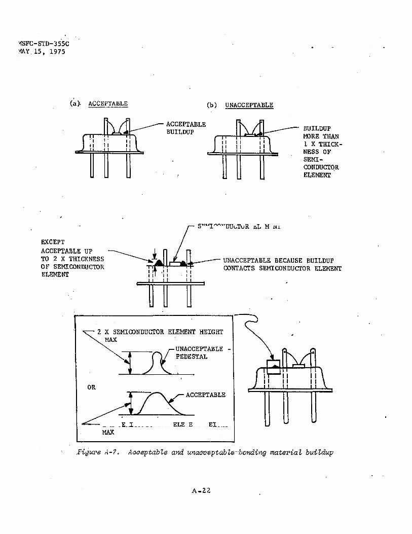
20 .2 .4 Semiconductor element mounting - The semiconductor element shall be mounted and bonded so that it is not tilted more than 10 degrees from the normal mounting surface. "Where the bonding agent accumulates around the perimeter ot the semiconductor element and touches the side ot the semiconductor element, it shall not accumulate to a thickness greater than the thickness oi the semiconductor elements. Where bonding agent is built up but is not touching the semiconductor element, the build-up shall not be greater than twice the thickness of the semiconductor element nor have a pedestal form. See Figure A-7.
20. 2. 5 Extraneous material - There shall be no visible ex-traneous material or foreign objects 0.0254 mm (0.001 in.) or larger in the major dimension; loose bonding (eutectic) material will be con-sidered extraneous material., See Figure A-8(b). Excessive (but not loose) bonding material will not be considered extraneous unless it fails to meet the requirements of 20. 2. 4_£See Flgure-A=7).
A-16

MSFC-STD-355C MAY 15, 1975 '
20. 2. 6 Clearance - Acceptable transistors shall exhibit ade-quate internal clcarances. The minimum distance between electrical connections on the post (or the post proper) and the nearest point on the ease or header, as well as the minimum distance between the load wire and the case or header, shall be equal to the diameter of the element post proper (except for the short distance between lead and header in the vicinity of the bond of the lead to the semiconductor element). When a low profile*case (such as a TO-46) is a specific design requirement, clearance shall be 20 percent of the total inside dimension between the base and top of the case. In transistors that have the semiconductor element mount vertical, the minimum clearance shall be 0. 0508 mm (0, 002 in. ) between the semiconductor element mount and header, and between the semiconductor element mount and case (see Figure A-9) .
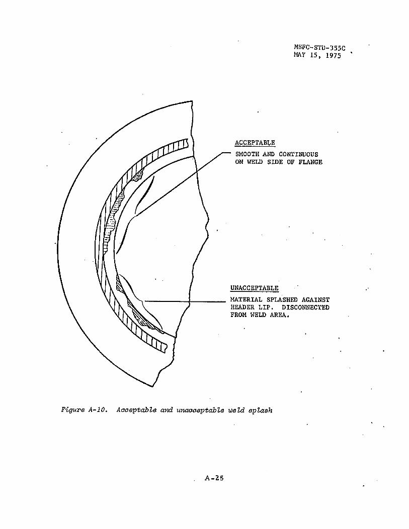
20. 2. 7 Weld splash - There shall be no indication of weld splatter in the form of balls or strips on the inside of the device, Weld expulsion, when continuous and uniform, is acceptable when located on the weld ring side "Of the header (see Figure A-10).
20, 2. 8 Excess material - There shall be no excess eutectic material on the semiconductor element, on the case, on the lead weld, nor separated from the original bond line (see Figure A-ll) .
20. 2. 9 Quad transistors, metal box package - In addition to the examination criteria listed above, quad transistoi*s shall also be examined for the following criteria.
20. 2. 9. 1 Extraneous material - There shall be no detectable loose particles 0.0254 millimeter (0.001 in.) or larger in the major dimension. A loose particle shall be defined as one which changes location when the package is rotated 180 as shown in Figure A-12(a),
20. 2. 9. 2 Substrate attach voids - Contact area voids under the substrate (carrier) in excess of 20% of the total-contact area are un- ' acceptable.
2 0 . 2 . 9 . 3 Internal clearances - Clearance between internal ends of feedthru pins of less than one pin diameter is unacceptable. See Figure A-12(b).
• Q 2 0 . 2 . 9 . 4 Bent pins - Feedthru pins deviating more than 10 from
a straight line are unacceptable. See Figure A-12(c).
A-26

MSFC-STD-355C MAY 15, 1975 '
ACCEPTABLE
M.'iii ACCEPTABLE BENDS ON WIRE
UNACCEPTABLE
UNACCEPTABLE - SHARP BENDS
_ t -Figure A-2, Acceptable and unacceptable bends ori internal leads
i
A-26

MSFC-STD-355C MAY 15, 1975 '
^ B
(b) ACCEPTABLE IF B = 3 TO 5 DTAMKTKRS FOR 0.127 MM (.005 FN.) TO 0.-254 MM (.010 IN.) WIRE OF B = 7 TO 10 DIAMETERS FOR WIRU LESS THAN 0.127 MM (.005 IN.) IN DIAMETER,
UNACCEPTABLE IF DISTANCE A EXCEEDS 3 TIMES DIAMETER OF WIRE CONNECTING POST TO SEMICONDUCTOR ELEMENT
rn & II II
II II I I
UNACCEPTABLE - WIRES SAG TOO MUCH AM) TOO CLOSE TO SEMI-CONDUCTOR ELEMENT
Figure A-3. Acceptable and unacceptable bent or sagging internal leads
A~19

-STD-355C 15, 1975-
Figure A-4, Other types of acceptable and unacceptable internal leads
A - 2 0

MSFC-STD-355C MAY 15, 1975
I I I JLl
UNACCEPTABLE MISALIGNMENT
! I JLL 1
Figure A-5. Misaligned internal leads
(A) UNACCEPTABLE PIGTAIL > 1/2 Y
(B) UNACCEPTABLE - WIRE LEADS TOO LONG
Figure A-6, Internal leads too long
A - 2 1
-STD-355C 15, 1975
(a> ACCEPTABLE (b) UNACCEPTABLE
M ' I I 11 > 1 1 ( I I I 1 M M 1
ACCEPTABLE BUILDUP p-
11 11 JLL
1 l I I JJ_ a BUILDUP MORE THAN 1 X THICK-NESS OF SEMI-CONDUCTOR ELEMENT
EXCEPT ACCEPTABLE UP TO 2 X THICKNESS OF SEMICONDUCTOR ELEMENT
SEMICONDUCTOR ELEMENT
UNACCEPTABLE BECAUSE BUILDUP CONTACTS SEMICONDUCTOR ELEMENT
2 X SEMICONDUCTOR ELEMENT HEIGHT X . MAX
r-UNACCEPTABLE -i k C \ f PEDESTAL
i A OR
r ~ r s < r ~
2 X SEMICONDUCTOR ELEMENT HEIGHT MAX
.Figure A-?. Aoaeptable and unacceptable-bonding-material buildup
A - 2 2

MSFC-STD-355C MAY 15, 1975 '
(a) ACCKPTAiiLli
NO EVIDENCE OF BROKEN WIRES AND LOOSE OB-JECTS 0.0254 MM (0.001 IN.) OR LARGER
EUTECTIC BUILDUP JOINED WITH ORIGINAL BOND LINE
(b) UNACCEPTABLE
PARTICLE 0.0254 MM (0.001 IN.) OR LARGER
BROKEN LEAD
©
©
EUTECTIC SEPARATED 'FROM ORIGINAL BOND LINE
Figure A-8. Acceptable and unacceptable foreign objects
A - 2 6

MSKC-STD-JS^C MAY J1), J975
Figure A-9. Unacceptable internal clearance.
A - 2 4
MSFC-STD-355C MAY 15, 1975 '
Figure A-10* Acceptable and unacceptable weld splash
A - 2 6

MSFC-STD-355C MAY 15, 1975 '
ACCEPTABLE
UNACCEPTABLE
EUTECTIC BUILT UP ON CASE
EUTECTIC ON LEAD WELD
EUTECTIC ON SEMI-CONDUCTOR ELEMENT
EUTECTIC SEPARATED. FROM ORIGINAL BOND LINE
Figure A~ll» Acceptable and unacceptable excess material
A - 2 6

MSrc—STI>-355c: MAY 15, ] 975
ACCEPTABLE ATTACHED PARTICLE
^—PARTICLES
UNACCEPTABLE LOOSE PARTICLE
(INITIAL) VIEW 1 "(a) PARTICLE CONTAMINATION
©
©
<S>
UNACCEPTABLE - PIN SEPARATION LESS THAN ONE PIN DIAMETER
I
I
(ROTATED 180*) VIEW 2
ACCEPTABLE -GREATER THAN METER
SEPARATION 1 PIN DIA-
UNACCEPTABLE -PIN BENT MORE THAN 10°
UNACCEPTABLE - PIN BENT MORE THAN 10°"
(b) PIN CLEARANCE (c) BENT PINS
Figure A-12. Acceptable and unacceptable workmanship for metal box can quad transistors
A - 2 7

MSFC-STD-3 5 5C MAY 15, 1975
APPENDIX B INTEGRATED CIRCUITS
10. SCOPE
10.1 This appendix establishes the criteria for acceptance and rejection of integrated circuits supplied under the provisions of this standard.
20. • Views
20.1.1 Round can type (TO-5 etc.) cases - Three views shall hp taken. One view shall be taken with X-rays penetrating the case normal to a plane passing through lead number one. Using lead one as an axis, rotate the device 90 degrees and take a second view. A third view shall be taken along the Y-axis. (The Y-axis is the cylindrical axis.)
20.1.2 Flat pack or dual-in-line - Two views shaU be taken. . One view shall be taken with the X-rays penetrating the case normal to the main axis (perpendicular to the plane of the chip), A second view shall be taken with the X-rays penetrating a side (preferably a side containing no leads).
20.2 Examination - The integrated circuit examination shall include, but not be limited to, inspection for foreign particles, build-up of bonding material, proper placement of lead wires, proper bond of lead to semiconductor element and lead to terminal post, accuracy of semiconductor element geometry, and mounting of semiconductor ele-ment.
20 .2 .1 Presence of extraneous matter - Extraneous matter that shall be cause for rejection shall include, but not be limited to:
(a) Any particle greater than 0.0254 mm (0.001 in.) See Figure B-l(a).
(b) Any wire extending more than 0.0762 mm (0.003 in.) beyond its bond. See Figure B-l(a).
(c) Any burr on a post (header- lead) greater than 0. 0254 mm (0. 001 in.) in its major dimension.
(d) Excessive semiconductor element bonding material buildup.
(1) A semiconductor element shall be mounted and bonded so that it is not tilted more than 10 degrees from the normal mounting surface. Where the bonding agent accumulates around the perimeter of the semiconductor element and
B - 2 9

touches the side of the semiconductor element; it shall not accumulate to a thickness greater than that of the semiconductor element. See Figure B-2(b). Where the bonding agent is built up but is not touching the semiconductor element, the buildup shall be not greater than twice the thickness of the semi-conductor element. See Figure B-2(c).
(2) There shall be no visible extraneous material 0.0254 mm (0.001 in. ) or larger in the major dimension. Loose bond-ing material will be considered extraneous material. Excessive (but not loose) bonding material will not be considered extraneous unless it fails to meet the require-ments of 20.2 .1 (d) (1) or if the accumulation of bonding material is in the pedestal form. See Figure B-3(b).
(e) Gold flaking on the header'or posts or anywhere inside the case.
2 0 . 2 . 2 Inadequate or abnormal construction - In the examination of integrated circuits, the following aspects, among others, shall be considered inadequate or abnormal construction:
(a) Contact area voids in excess of one-fourth of the total contact area. See Figure B-l(b).
(b) A s ingle void equal to the length of the semiconductor, element or single void that traverses the entire width of the semiconductor element. See Figure B-l(b).
(c) A single void in the die attachment area opening on two adjacent sides of the die and extending under two' or more bonding pads of the die. See Figure B-l(c).
(d) Extraneous ball bonds attached to the semiconductor element.
(e) Wires present other than those connecting specific areas of the semiconductor element to the external leads, except where the design of the integrated circuit calls for the use of such additional wires, or the jumper wires necessary to trim load resistors- See Figure B-l(a).
(f) Inadequate clearance. Acceptable devices shall have adequate internal clearances to assure that the elements cannot contact one another or the case. Depending upon the case type, devices shall be rejected for the following conditions:
B-30

MSFC-STD-355C MAY 15, 1975
(1) Flat pack and dual-in-line.
(a) Any ball bond that is less than 0. 0254 mm 0, 001 in.) from another bond (Y plane only). See Figure B-4(a).
(b) Any lead wire which has less than two wire diameters separation from another lead wire at a distance of 0.254 mm (0,010 in.) or greater from the die bond (Yplane only). See Figure B~4(e).
(c) A lead wire which crosses over another bond or lead wire (Y plane only). See Figure B-4(c).
(d) Any lead wire within two wire diameters of the case or external lead to which it is not attached (X and Y plane). See Figure B-4(d).
(e) Clearance between the lead frame and metal package of less than three wire diameters. See Figure B-4(b).
(f) Any lead wire where bow is less than 7 or more than 10 lead wire diameters from a straight line as drawn from the pad bond to the post bond (X plane only). See Figure B-5,
(2) Round transistor can (TO-5 etc) type (see Figure B-6) .
(a) Any lead wire within 0.127 mm (0.005 in.) of the case or external lead to which it is not attached (X and Y plane),. See Figure B-6(a).
(b) Lead wires which sag below an imaginary plane across the top of the bond (X plane only). See Figure B-6(b).
(c) Any ball bond which is less than 0, 0254 mm (0. 001 in . ) from another bond (Y plane only). See Figure B-6(c).
(d) Any lead wire which has less than two wire diameters separation from another lead wire at a distance of 0 .254 mm. (0.010 in.) or greater from the die bond (Y plane only). See Figure B-6(f).
(e) Any lead wire that crosses over another bond or lead wire (Y plane only). See Figure B-6(d) and (e).
B - 3 7

Any lead wire where bow is less than 7 or more than 10 lead wire diameters from a straignt line as drawn from the pad bond to the post bond (X plane only). See Figure B-6(g).
B - 3 0

MSFC-STD-355C MAY 15,.1975
UNACCEPTABLE 0,0762 MM (U.003 IN.)
UNACCEPTABLE
F-tguie. 6 -1 . PaAticZe. locatioyiA, plQtcuUU £Kimnln$ wajiqa and void*
B 3 3

MSFC-STD-355C - ! MAY 15, 1975
UNACCEPTABLE
A C C E P T A B L E BUILDUP
BUILDUP MORE THAN 1 X THICKNESS OF SEMI CONDUCTOR ELEMENT
(a) <b)
SEMICONDUCTOR ELEMENT
A C C E P T A B L E UP TO 2 X THICKNESS OF SEMICONDUCTOR ELEMENT
UNACCEPTABLE BECAUSE BUILDUP CONTACTS SEMICONDUCTOR ELEMENT
(c)
Figure 2. Acceptable and unacceptable bonding material buildup
B -34

MSFC-STD-355C MAY 15, 1975
(a)
Figure B-3. Extraneous bonding material buildup
B - 3 7
\

MSFC-STD-355C MAY 15, 1975
(a) BALL BOND WITHIN 0.0254 MM (0.001 IN.) OF OTHER BOND
(c) LEADWIRE CROSSES ANOTHER WIRE
LESS THAN THREE WIRE DIAMETERS CLEARANCE BETWEEN LEAD FRAME AND METAL PACKAGE
LEADWIRE WITHIN TWO WIRE DIAMETERS OF EXTERNAL LEAD
to Ai
(e) SLACK WIRE WITHIN TWO WIRE DIAMETERS OF ANOTHER WIRE
( f ) LEADWIRE CROSSES OVER A BOND
Figure B-4. Unacceptable clearance in dual-in-line and flat pack type devices
UNACCEPTABLE IF BOW IS LESS THAN 7 LEAD DIAMETERS OR GREATER THAN 10 LEAD DIAMETERS
Figure B^S. Unacceptable lead wire bow
E-37

MSFC-STD-355C MAY 15, 1975
(a) LEAD WIRE WITHIN 0.127 MM (0.005 IN.) OF CASE
(b) SAGGING LEAD WIRE
s \ » \ \ / J
(g) UNACCEPTABLE IF BOW IS LESS THAN 7 LEAD WIRE DIAMETERS OR GREATER THAN 10 LEAD WIRE DIAMETERS
(c ) BALL BOND WITHIN 0.0254 MM <0.001 IN.) OF ANOTHER BOND
(d) LEAD WIRE CROSSES OVER ANOTHER WIRE
(e) LEAD WIRE CROSSES OVER A BOND
( f ) SLACK WIRE WITHIN TWO WIRE DIAMETERS OF ANOTHER WIRE
Y-AXIS CLEARANCE
Figure B-6, Unacceptable clearance in round transistor can type
B - 3 7

MSFC~STD~355C MAY 15, 1975
APPENDIX C DIODES
10. . SCOPE
10.1 This appendix establishes the criteria for acceptance and rejection of diodes supplied under the provisions of this standard.
20. REQUIREMENTS
20.1 Views
20.1.1 Tubular parts - Two views , normal to the major axis of the part, shall be taken. One view shall be 90 degrees from the other. If deemed necessary by the testing laboratory or by the MSFC represen -tative, a third view shall be required.
20.1. 2 Voidless butt constructed diodes - Three views as shown in Figure C - l shall be taken of voidless butt constructed diodes,
(B) VOIDLESS BUTT CONSTRUCTED DIODE ,
Figure C - l
20 ,2 Examination - The diode examination shall include, but not be limited to, inspection for extraneous material, solder splash, proper shape and placement of lead wires or whiskers, proper bond of lead or whisker to semiconductor element and lead or whisker to terminal post, proper bond of Semiconductor element to header, and accuracy of semiconductor element geometry.
20. 2 .1 Lead wire - The lead wire or whisker shall not extend beyond the post bond by a distance greater than twice the diameter of the wire. There shall be no loops or excessive bends in the lead wire.
C-41
-355C 1975
20. 2. 2 Extraneous material - There shall be no loose or at-tached extraneous material 0 .0254 mm (0,001 in.) or larger in size. Excessive or loose semiconductor element bonding material shall be considered extraneous material.
,20 .2 .3 Clearance - Acceptable devices shall have the follow-ing adequate clearances.
2 0 . 2 . 3 . 1 Whisker - The minimum distance from the whisker to the case shall be equal to 1/2 the diameter of the external lead wire. See Figure C-2 .
20. 2. 3. 2 Bonding material - The minimum distance from the semiconductor die or any eutectic bonding material to the case shall be 0.0508 mm (0 .002 in.) See Figure C-3 .
2 0 . 2 . 4 Whisker deformities - Diode whisker deformities shall be limited to the following:
(a) The diode whisker shall not be tilted more than 5 degrees in any direction from the diode lead axis.
(b) The whisker shall not be deformed to the extent that it touches itself. .The minimum air gap between any two points on the S-shaped whisker shall be twice the diameter or thickness of the whisker wire.
2 0 . 2 . 5 Monolithic case construction (whiskerless)
(a)' The anode and cathode lead connections shall not be displaced more than 0. 254 mm (0.01 in.) wfth respect to the central axis of the device.
(b) The semiconductor element shall not be misaligned (see 20.2 , and Figure C-5) .
(c) Any glass void (bubble) that exceeds 0 .254 mm (0.010 in.) in any dimension shall not be acceptable (see Figure C-7) .
2 0 . 2 . 6 Misaligned diode semiconductor element - The diode semiconductor element mount shall not be tilted more than 15 degrees from normal to the main axis of the diode (see Figure C-4) .
2 0 . 2 . 7 Overhanging diode semiconductor element - In glass diodes, the semiconductor element (die) shall not hang over the edge of the header by more than 10 percent of the totarl area of the semi-conductor element.
C - 4 0

MSFC~STD~355C MAY 15, 1975
20 „ 2. 8 Chipped glass - Any visible indication of glass missing on the body or lead exterior or interior surface shall be rejected if the major axis of the chipped glass is greater than 0.127 mm (0.005 in,).
20. 2. 9 Semiconductor e lement mounting - A minimum of 90 percent of the semiconductor e lement base area shall be bonded to the mounting sur face .
20. 2.10 Lead welds - The welds between the leads and the heat sink slugs on double heat sink (voidless butt construction) devices shall be examined for porous, blown, fractured, or incomplete welds. . Voids in the weldment shall not extend more than 15 percent of the lead wire diameter from any edge, and there shall be no voids whatever in the central part of the area that should be welded. See Figure C - 6 .
C - 4 1

MSFC-STD-355C MAY *15, 1975
D" LEAD DIAMETER
DIE SURFACE
Figure C-2. Minimum whisker clearance zone
SEMICONDUCTOR J>IE — 0,0508 MM (0.002 IN.) MINIMUM
121 > 1 E 0.0508 MM (0.002 IN.) MINIMUM EUTECTIC BONDING MATERIAL
Figure C-3. Minimum bonding clearance
UNACCEPTABLE - SEMICONDUCTOR ELEMENT MOUNTING TILTED MORE THAN 15 DEGREES FROM NORMAL TO MAIN AXIS
Figure C-4. Unacceptable semiconductor mounting
C - 4 Z

MSFC-STD-355C MAY 15, 1975
>15°
15 DEGREES NORMAL TO MAIN AXIS
'Figure C-5. Unacceptable monolithic dual heat sink diode
Figure C-6. Unacceptable weld voids
UNACCEPTABLE GLASS VOID
C-.43

MSFC-STD-355C MAY 15, 1975
APPENDIX D RESISTORS
10. SCOPE
10.1 This appendix establishes the criteria for acceptance and rejection of insulated film, high stability encapsulated film, wire wound power, and wire wound accurate resistors supplied under the provisions of this standard.
20. REQUIREMENTS
20.1 Views - Two views, normal to the major axis of the part, shall be taken. One view shall be 90 degrees from the other. If deemed necessary by the testing laboratory or by the MSFC representative, a third view shall be required.
20.2 Examination - The resistor examination shall include, but not be limited to, inspection for extraneous material on the resistance element or within the enclosure, misaligned or mispositioned resistor core, misaligned electrodes or end caps, and physical damage of electrical elements of the resistor. Refer to Figure D- l and D-2 for insulated film constructed examples, Figures D - l through D-4 for high stability resistors, Figures D-5 and D-6 for wire wound power resistors, and Figures D-5 and D-7 for wire wound accurate resistors.
20. 2.1 Extraneous material - There shall be no loose or at-tached extraneous material 0.0508 mm (0.002 in or larger in size on the resistance element, windings, or within the enclosure. See Figures D-l(a), D-6(b), and D-7(c).
20. 2. 2 Misaligned core - The core shall be aligned within 5 degrees of a line connecting the centers of the two electrical connections. See Figures D-6(j), and D-7(f).
20. 2. 3 Mispositioned core - Core positioning shall be as specified herein for each specific type of resistor.
2 0 . 2 . 3 . 1 Insulated film and high stability film resistors - The core of the resistors shall not be positioned less than 75% of the maximum possible distance into each end cap nor shall it be fully in* serted (bottomed). Cores that are inserted less than 75% shall be rejected. See Figures D-2(b) and D-6(e).
20, 2. 3. 2 Wire wound power and accurate resistors - The core of,the resistor shall be positioned in accordance with Figure D-5 , Dimension A shall be 30% to 70% of A plus B. Diminsion C shall be 40% to 60% of C plus D. In addition, the core shall be positioned into
D-45

each end cap a distance equal to 75% or greater of the depth of the cap. Cores not inserted 75% or greater shall be rejected.
2 0 . 2 . 4 Misaligned electrode - The center lines of the internal electrodes shall not form an angle greater than 5 degrees. See Figure D-6(j).
20. 2. 5 Physical damage - There shall be no visible cracks, splits, or chips from the core or resistive material of any resistor. See Figures D-l(b), D-6{a), and D-6(f).
20 .2 .6 End Caps - End caps shall fit closely onto the core and shall be aligned with the core within five degree maximum. No voids shall be visible between the inner edge of a round end cap and the core material. Hexagonal or octagonal end caps shall contact the core at a point along each flat of the end cap. Cracked, undersize end caps shall be cause for rejection, See Figures D-2(a), (d), and (e), D-3(a); D-6(d); and (i); and D-7(d), (e), and (g).
20 .2 .7 Talon type leads - Talon type Leads are unacceptable. All parts containing talon leads shall be rejected,
20 .2 .8 Misaligned leads - The center line of the leads shall not form an angle greater than 5 degrees.
20. 2. 9 Windings - Examination of wire wound 'resistors shall be as follows.
20.2.9.1" Power resistors - The windings of the resistor ele-ment on the core shall be uniformly spaced within one ribbon width for flat wire and within two wire diameters for round wire. Also, minimum acceptable .winding to winding spacing shall be one-half the width of the ribbon or one wire diameter. Furthermore, no gap shall be visible between the ribbon and the core. See Figure D-6(c).
20. 2. 9. 2 Accurate resistors - Each coil shall have approximately the same number of turns of wire and be on the same style and size bobbin. There shall be no cocked bobbins. In addition, there shall be no excessively loose turns visible on a coil. A separation of 0. 25 mm (0. 010 in.) or more between a winding and the next inner layer of wind-ing shall be considered excessive. See Figures D-7(a), (b), (j) and (k).
. •» ' *
20.2.10 Lead weld - The external lead-wire-to-end-cap weld shall be uniform and no gap shall be visible between the end of the lead wire and the face of the end cap. See Figure D-2(c) and D-6(h).
D-46

MSFC-STD-355C MAY 15, 1975
(0.002 IN.)
Figure U-l. Unacceptable workmanship for insulated film and high stability encapsulated film resistor core
INADEQUATE FIT
(e) CRACKED END CAP (d) END CAP CANTED > 5'
( c ) IMPROPER LEAD ATTACHMENT
Figure D-2, Unacceptable workmanship for insulated film and high stability encapsulated film resistors
D - 4 7

MSFC-STD-355C MAY 15, 1975
(a) DAMAGED END CAP
Figure D-3, Unacceptable workmanship for high stability encapsulated resistors
UNACCEPTABLE TALON LEAD
ViQWia V-4. Talon lead con&tmiction - unacceptable
A « 30 TO 70% OF A + B C = 40 TO 60% OF C + D
Figure D-S. Core positioning for molded wire wound resistors
D-48

MS FC- 8T0- 3 5 Mi MAY 15,
(a) CRACKED OR DAMAGED CORE \
(b) PARTICLE >_ 0,0508 MM (0.002 IN.) LARGEST DIMENSION
( c ) * TURNS NOT EVENLY SPACED
C
( f ) DAMAGED WIRE ELEMENT
(h) ENDCAP SEPARATION
( i ) CRACKED ENDCAP
J ( d ) OVERSIZE ENDCAPS
(e) INCOMPLETE
5°
END CAP f f INSERTION • (< 75%) ~
(g) LEADS OUT OF ALIGNMENT > 51
( j ) CORE MISALIGNMENT
a r )
a j
)
Figure D-6. Unacceptable workmanship for wire wound power resistors
D - 4 9

MSFC-STD-355C MAY 15, 1975
(k) COCKED BOBBIN
( i ) CORE NOT CENTERED PER D-5 i f t J U U U ^ =
Figure V-7. Unacceptable workmanship for wire wound accurate resistors
D-50
MSFC-STD-355C MAY 15, 19.75
APPENDIX E
CAPACITORS
10, SCOPE
10, 1 This appendix establishes the criteria for acceptance and rejection of solid tantalum, non-solid tantalum, tantalum foil, hermetically sealed plastic, paper, and paper/plastic and ceramic capacitors supplied under the provisions of this standard.
20. REQUIREMENTS
20. 1 Views
20. 1.1 Tubular units - Two views, normal to the major axis of the part, shall be taken. If deemed necessary by the testing laboratory or procuring activity representative, additional views shall be required*
20. 1.2 Flat chip units' - One view shall be taken normal to the plane of the chip.
20. 2 General examination - The examination for all capacitors shall include, but not be limited to, inspection for faulty lead connections, misalignment of internal parts, solder or weld defects, and physical damage of electrical elements.
20.2. 1 Faulty lead connection - There shall be no evidence o/ improperly made lead connections.
20 .2 .2 Misaligned parts - Criteria for rejection due to mis -alignment of anodes, seals, eyelets, or spacers shall be as specified in the detail examinations below.
2 0 . 2 . 3 Solder defects - Criteria for rejection due to solder-ing defects shall be as specified in the requirements for individual capacitors given below.
2 0 . 2 . 4 Physical damage - There shall be no holes, cracks, splits, or chip8 of electrical elements,
20. 3 Specific examinations - Examinations that are peculiar to the individual capacitor types in addition to the general examinations, are listed below. All capacitors failing to meet these requirements shall be rejected. Examples of typical defects, as well as acceptable devices, are shown,
E - 5 1

20. 3. 1 Solid tantalum - Figure E - l shows acceptable variations which are normal. Unacceptable defects which may cause capacitor degradation or failure during periods of electrical, mechanical, or environmental stress are shown in Figure E~2.
20. 3 . 1 . 1 Tubelet solder defects - Defects which are peculiar to the tubelet and can be induced during anode lead retinning.or when mounting the capacitor on the printed circuit board are shown in Figure E - 3 .
2 0 . 3 . 1 . 2 Non-polar capacitor defects - All the proceeding reject criteria for polarized capacitors applies also to non-polarized capacitors. Non-polars consist of two polars, soldered back-to-back in a common metal sleeve. Internal solder reflow of the polars is possible during manufacturing as shown in Figure E-4 .
20. 3. 2 Non-solid electrolyte tantalum slug - This section con-tains specific reject criteria for non-solid tantalum slug capacitors. See 'Figure E-5 for acceptable and unacceptable workmanship.
20. 3. 2. 1 Metallic particles - There shall be no metallic particles within the case. Refer to Figure E-5(b).
2 0 . 3 . 2 . 2 Tilted slug - Tilted slugs are unacceptable if the slug shoulder is touching the inside of the case. See Figure E-5(d).
2 0 . 3 . 2 . 3 Bent leads - Leads having an "S " shaped bend are unacceptable regardless of the cause or the position of the capacitor slug. See Figure E-5(d)> Leads bent in a smooth arc are acceptable if there ' are no nicks, gouges, necked-down areas or other defects of the lead.
, 2 0 . 3 . 2 . 4 Off-center slug - The allowable amount of off -centering will vary with case size and manufacturer. Noticeable off-centering beyond manufacturer's tolerance or uncommon to the lot average shall be cause for rejection of the capacitor. Off-centering that reduces the normally available spacing between capacitor slug and case by 25 percent or more shall be cause for rejection. See Figure E-5(e).
20. 3. 2. 5 Physical damage - There shall be no evidence of a chipped or cracked anode or other physical damage to the tantalum slug. Refer to Figure E-5(e).
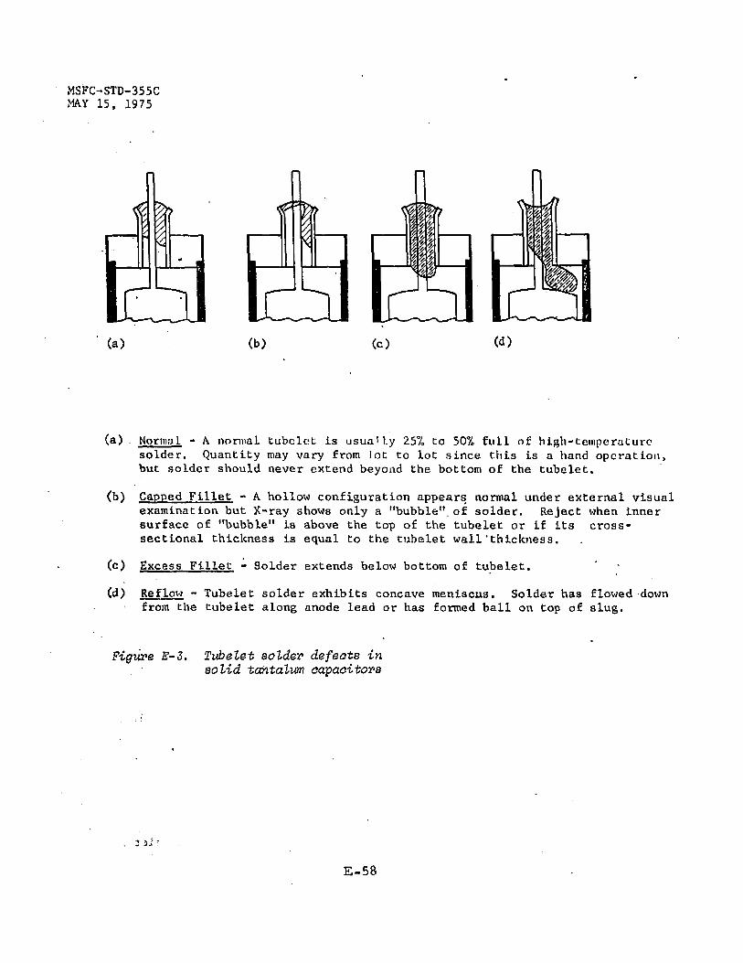
2 0 . 3 . 3 Hermetically sealed tantalum foil capacitors - This section contains X-ray reject criteria for hermetically sealed tantalum foil capacitors. Typical examples of acceptable and unacceptable tantalum foil capacitor X-rays are shown in views (a) through (e) of Figure E - 6 .
2 0 , 3 . 3 . 1 Telescoping of foil - Although the allowable amount of telescoping will vary with the manufacturer and case size, noticeable telescoping uncommon to the lot average shall be cause to reject the capacitor. See Figure E-6(b).
E - 5 2
MSKC-tfTD-r/iC MAY 15, I97'i
20, 3. 3. 2 Metallic foreign particles - Metallic foreign particles shall be cause for rejection if the largest dimension of any one particle or the sum of the largest dimensions of several particles exceed 0* 010 inch (0.254 mm). See Figure E-6(c) .
20, 3. 3. 3 Lead defects - The portion of the internal lead which is perpendicular to the axis of the capacitor roll shall be no less than
"0. 8 mm (0. 032 inch) from the closest edge of the foil whether the foil is telescoped or not. See Figure E-6(d),
2 0 . 3 . 3 . 4 Off-center capacitor element - Off-center capacitor elements shall be rejected if a lead is crumpled as shown in Figure E-6(e). The capacitor shall also be rejected if the distance A is equal to or less than one-half the distance B whether the lead is crumpled or not.
2 0 . 3 . 4 Hermetically sealed, paper, plastic, paper/plastic dielectric capacitors - This section contains X-ray reject criteria for hermetically sealed capacitors containing dielectrics which may consist of paper, *plastic, or paper/plastic combinations. Typical , examples of acceptable and unacceptable capacitors are shown in Figure E - 7 .
2 0 . 3 . 4 . 1 Extraneous material - Any metallic particle discernible within the capacitor section shall be cause to reject the part. See Figure E-7(b). Any single foreign particle larger than
^ 0. 1524 millimeters (0.006 inch) in its longest dimension, regardless *bf location, shall be cause to reject the part. See Figure E-7(c) . A string of particles less than 0. 1524 millimeters (0. 006 inch) in diameter located between the section and case parallel to the axis of the sec-tion and which are continuous for more than 1 /4 of the section length shall be cause to reject the part. See Figure E-7(d). Random end spray particles
>lwhich are less than 0. 1524 millimeters (0. 006 inch) in diameter are typical of these capacitors and shall not be cause for rejection. Foreign'
^particles, looped wire, metallization, or excess solder from the end spray cap shall not extend into the capacitor element when measured from the base of the end spray cap (refer to views (e) and (f) of Figure E-7) .
/ 2 0 . 3 . 4 , 2 Spikes and excessive solder - Spikes of end spray or solder other than described above shall not extend in any direction
r (refer to view (g) of Figure E - 7 ) . Solder in excess of the amount shown " i n Figure E-7(a) and (e) shall be considered excessive (refer to view (h) * of Figure E-7 ) .
20. 3. 4. 3 Lead wire bends - Units having the internal lead wire bent shall be rejected (refer to view (i) of Figure E-7) .
2 0 . 3 . 4 . 4 Tubelet sealing - Excess solder from tubelet sealing located within the case and on the lead wire shall be cause for rejection (refer to view (j) of Figure E - 7 ) .
E - 5 3

.i; -STD-355C 15, 1975
2 0 . 3 . 4 . 5 Misal ignment - Extreme misal ignment or improper positioning of the sect ions within the case shall be cause for re jec t ion (refer to view (k) of Figure E - 7 ) .
20. 3. 5 Non-hermet i c c e r a m i c - This sect ion contains re jec t cr i ter ia f o r non-hermet i c c e r a m i c d ie lec t r i c capaci tors with leads internally so ldered or welded to the capacitor chip.
20. 3. 5. 1 E x c e s s so lder - Solder coating on the leads shall not extend beyond the normal configuration shown in v iew (a) of F igure E - 8 . Excess so lder shall be cause f o r re ject ion .
20. 3 . 5 . 2 Insufficient lead attachment - There shall be no gap (lead separation) in the bond of wire to capaci tor chip. An example of this dofoct is shown in v iew (h) of F igure E - 8 .
20. 3. 5. 3 Damaged loads - There shall be no damage such as nicks or gouges, on either lead (See (c) of F igure E - 8 ) ,
20. 3. 5. 4 Chipped c e r a m i c or e lec trode - There shall be no chipped areas along the c e r a m i c o r capaci tor e l e c t rodes . An example . is shown in v iew (d) of F igure E - 8 .
20. 3. 5. 5. E x c e s s swaging - Reduction in thickness of swaged capacitor leads shall not extend beyond the attachment to the capacitor ship m o r e than 10 percent of the length of attachment (See v iew (e) of Figure E - 8 ) . '
2 0 . 3 . 5 . 6 Element misal igned o r o f f - c e n t e r - The capacitor element shall be aligned in such a manner that it is complete ly embedded in the encapsulant. Capacitor elements that a r e misal igned to the extent that one edge is exposed as indicated by the radiograph, are unacceptable (See (f) of F igure E - 8 ) .
2 0 . 3 . 6 E x c e s s i v e heat - When inspecting mounted capaci tors , l ook f o r evidence of ex cess ive heat, which will be indicated by so lder re f low in the tubelet a rea . Any such evidence shall re jec t the capaci tor and should result in an investigation of the capacitor installation procedures . All hermet i ca l ly sealed so lder - tubelet type capacitors should
' be considered heat -sens i t ive , requiring careful control of lead retinning, installation using heat -s inks , and care during any subsequent rework.
E - 5 4

MSFC-STD-355C MAY IS, 1975
ACCEPTABLE
r = f
¥ (a) NORMAL
> = f l = i
^yyyyyyy//, u (b) MAXIMUM
SOLDER
r-J fcr
¥ (c ) MINIMUM
SOLDER (d) OFFSET
SOLDER (e) OFFSET
SLUG
ACCEPTABLE - MINOR DEFECTS PI J i b ¥
( f ) SOLDER FLOW (g). SOLDER VOIDS (h) EXCESS SOLDER ( i ) COCKED SLUG
NORMAL SOLDER FILLET PLUS FLOW DOWN CASE WALL.
SLUG COVERAGE WITH SOLDER AT LEAST 60%. ' VOID AT BOTTOM OF SLUG ONLY IF SIDES ARE WELL COVERED
TOP OF SLUG AND ANODE LEAD CLEARLY VISIBLE.
SLIGHT CURVE OF LEAD, AND SLUG NOT TOUCHING CASE.
Figure Acceptable solid tantalum capacitors
E - 5 5

MSFC-J»TDr355C MAY 15^ 1975
UNACCEPTABLE
1: I
I 1
z 3
o
t i
T (b)
^ fa
I
i /W77777fA
¥ (c )
d f fcl
T (d)
XJr
• .'^'.jfTJ } «•• •'* « *
(eP ' 1<
, . A (a; Insuf f i c ient Solder - Coverage only one s.ide and part of another. To bo aceo.pL-
rSiHe' solder must catch lower l e f t corner of slug base (sec E - l ( d ) ) . (b) Solder Ball - Round and dense in appearance. If adhered to case; w i l l appear to
move when second view is taken. I f loose, i t w i l l probably r o l l to lower side of can'and appear in same area as i t did in f i r s t view. Reject 0,01 inch or larger.
( c ) Stressed Lead - Bent during assembly, could cause damage to d i e l e c t r i c at vulnerable ?>|j^ad-s lug junc t ion.
(d) UOw' Solder - Usually the resul t , o f a too-small solder preform.
(e) Poor Splice Weld - Welds should be uniform and smooth, and aligned with the leads.
( f ) Cocked Header - Rejectable i f cocked to a noticeable degree and anode lead is v i s ib ly misaligned'.
(g) Cocked Slug - Upper shoulder of slug touching inside wall of case. V V ' *
(h) Header Solder Flow - Excess solder flow is indicated by a very dense image along .the'- lower edge of the solder but feathered-along the area c losest to the header. Rejectable when flow area approaches top shoulder of slug.
Figure^&Z * E-56
MSKC-STD-'J 55C MAY 15 > W 5
UNACCEPTABLE
fcn
T (1)
( i ) Excessive Solder - Either the upper port ion of the slug or the anode lead is obscured by solder . -
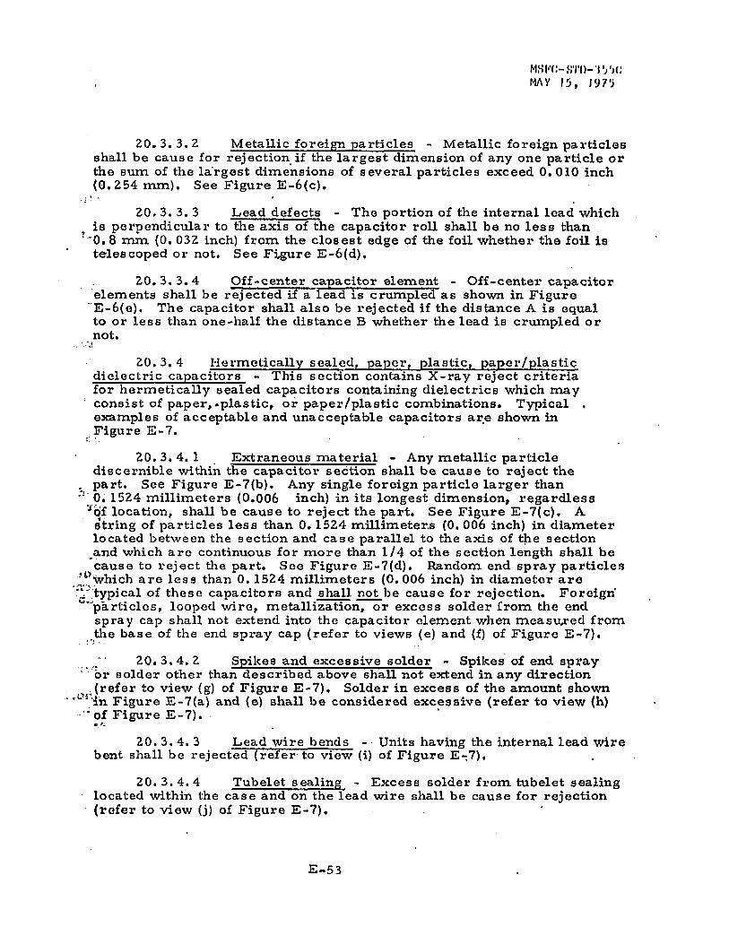
( j ) Insu f f i c i ent Solder - Extreme case of i n s u f f i c i e n t solder indicating marginal bond to case*.
(10 Broken Lead Weld - Could also indicate poor quality weld.
(1) No Solder in Case - Slug may be on bottom of case due to lack of solder preform during manufacture.
(m) High Slug - Slug " f l o a t i n g " on solder , may be touching header with inadequate solder tubelet closure above lead weld.
(n) Part ic les - Any irregular par t i c l e or pattern of par t i c l es exceeding 0.010 inch diameter.
(o) No Tubelet Solder - May perform ok e l e c t r i c a l l y during t e s t . Tubelet i s normally sealed by hand, and this operation could be overlooked.
Figure E-2 (aont)
E - 5 7
MSFC-STD-355C MAY 15, 1975
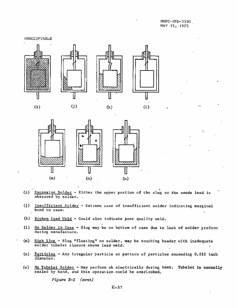
(a) Normal - A normal tubelet is usually 25% to 50% f u l l of high-temperature solder. Quantity may vary from lot to lot since this is a hand operation, but solder should never extend beyond the bottom of the tubelet .
(b) Capped F i l l e t - A hollow configuration appears> normal under external visual examination but X-ray shows only a "bubble", of solder . Reject when inner surface of "bubble" is above the top of the tubelet or i f i ts cross-sectional thickness is equal to the tubelet wal l ' thickness.
(c ) Excess F i l l e t - Solder extends below bottom of tubelet .
W) Ref.low - Tubelet solder exhibits concave meniscus. Solder has flowed down from the tubelet along anode lead or has formed ba l l on top of slug.
Figure E-3. Tubelet solder defeats in solid tantalum capacitors
z •
E - 5 8

MSFC-STD-355C MAY 15, 1975
ACCEPTABLE - WITH INTERNAL SOLDER ON BOTH SIDES OF SLUGS AND THE CONNECTING SOLDER RUNNING PART WAY UP THE OUTSIDE OF EACH CAN.
(b) UNACCEPTABLE - SHOWING INTERNAL SOLDER REMELTED AND ALL FLOWED TO ONE SIDE, ALSO LARGE LOOSE SOLDER PARTICLE,
( c ) UNACCEPTABLE - SHOWING CONNECTING SOLDER RUNNING ALL THE WAY UP ONE CAN BUT NOT TRAVELING UP THE SIDE OF THE OTHER CAN AT ALL,
Figure Non-polar solid tantalum capacitor defeats
E - 5 9

MSFOSTD-355C MAY 15, 1975
LEADWIRE SEAL
SPACERS
LEAD WELD (IP USPD)
TANTALUM SLUG (ANODE)
GEL-ELECTROLYTE
METAL CASE
LEADWIRE WELD
ACCEPTABLE CONSTRUCTION DETAILS
INCOMPLETE LEAD WELD
METALLIC PARTICLE
IMPROPER WELD
(B)
UNACCEPTABLE (O
UNACCEPTABLE
LAP OR IMPROPER LEAD WELD
I T (D)
UNACCEPTABLE
LEAD DEFORMED
TILTED BODY
(E) UNACCEPTABLE
BODY NOT CENTERED
PHYSICAL DAMAGE TO ANODE
FIGURE E 5 ACCEPTABLE AND UNACCEPTABLE WORKMANSHIP FOR NOH-SOLID TANTALUM CAPACITORS
E-60
MY J5, J975
V
ACCEPTABLE
FIGURE E 6 ACCEPTABLE AND UNACCEPTABLE HERMETICALLY SEALED TANTALUM FOIL CAPACITORS

MSFC-STD-355C MAY 15, 1975
UNACCEPTABLE
LAP WELD
UNACCEPTABLE
CRUMPLED LEAD (D)
FOREIGN PARTICLE
0.8mm
UNACCEPTABLE CRUMPLED LEAD
ELEMENT FAR OFF-CENTER LONGITUDINALLY i •
FIGURE E 6 (CONCL)
E - 6 2

MSFC-STD-355C MAY 15, 1975
11 I
0
(A) ACCEPTABLE (B) UNACCEPTABLE (C) UNACCEPTABLE
J> 1 I
J S"
4 ' . (E) ACCEPTABLE <F)UNACCEPTABLE (0)UNACCEPTABLE
FIGURE E 7 HERMETICALLY SEALED PAPER, PLASTIC, PA PER/PLASTIC CAPACITORS,
E - 6 3

MSFC-STD-355C
MAY 15, 1975 '
A (G) (H) (I)
SOLDER SPIKE EXCESSIVE SOLDER BENT LEAD
(J) (K)
SOLDER RUNOFF MISAUGNMENT FROM TUBELET
FIGURE E 7 (CONCL) UNACCEPTABLE PAPER, PAPER 'PLASTIC PLASTIC DIELECTRIC CAPACITORS.
E-64
CASE
CERAMIC BODY
(A) ACCEPTABLE
M S F C - S T D - 3 5 5 C
M A Y 1 5 , 1 9 7 5
(B) UNACCEPTABLE-LEAD SEPARATION
(C) UNACCEPTABLE-NICKED LEAD
(D) UNACCEPTABLE-CHIPPED
(E) UNACCEPTABLE EXCESS SWAGING
(F) UNACCEPTABLE - ELEMENT MISALIGNED OR OFF-CENTER
FIGURE E 8 ACCEPTABLE AND UNACCEPTABLE CERAMIC CAPACITORS.
E - 6 5

MSFC-STD-355C MAY 15, 1975
APPENDIX F
RELAYS
10. SCOPE
10. 1 This appendix establ ishes the c r i t e r ia f o r acceptance and re ject ion of re lays supplied under the prov i s i ons of this standard.
20. REQUIREMENTS
20. 1 Views - T h r e e v iews a r e required to show d e f e c t s . These shall be taken through the ' three main axes of the re lays as shown in F igure F - l . When inadequate c overage is pro.vided additional v i ews shall be taken as deemed n e c e s s a r y to sat is fy the c r i t e r ia defined here in ,
20. 2 Examination - The radiographic examination shall include, but not be l imited to, inspect ion f o r extraneous mater ia l ; parts al ignment, adjustments , and c l earances ; and i n c o r r e c t l y p e r f o r m e d operat ions . '
2 0 . 2 . 1 Extraneous mater ia l - T h e r e shall be no v i s ib l e e x -traneous mater ia l . . L o o s e o r e x c e s s i v e bonding mater ia l such as weld and so lder splash and so lder balls shall be cons idered extraneous mater ia l . Welded and so ldered joints shall be f r e e of l o o s e weld o r so lder f lash, o r attached f lash of ped ic le or lancet shape. F i r m l y attached e x c e s s i v e weld o r so lder f l ow i s acceptable provided it mee ts the dimensional requirements of F igure F -2 (b ) and F i g u r e F - 3 ( b ) . Examples of unacceptable extraneous mater ia l contamination a r e depicted in F igure F - 2 ( a ) .
2 0 . 2 . 2 Parts c l earance , adjustment, and alignment r Acceptab le relays sKall exhibit adequate internal e l e c t r i ca l and mechanica l c l e a r a n c e s . Cr i ter ia f o r determining adequate c l earance by inspect ion of radiographs shall be establ ished by each manufacturer and must be approved by the qualifying activity, except as spec i f ied o therwise here in . The bare end of co i l l ead w i r e s shall not extend beyond header pins m o r e than 1 .60 m m (0 .062 inch). C learances of any e lec tr i f i ed moving part f r o m the enc losure shall c o n f o r m to that spec i f i ed in F igure F - 3 ( b ) . A r m a t u r e and contact moving parts shall be f r e e of in ter ference with w i r e s o r other re lay par ts . Relay parts such as contact spr ings , bare co i l l eads , and actuator shall not touch header sur face . T h e r e shall be no e x c e s s i v e o r abnormal a i r gaps in joints between magnet ic c o r e and f r a m e parts such as can result f r o m i m p r o p e r parts al ignment. Examples of unacceptable parts c l earance , adjustment, and alignment a r e given in F igure F - 3 .
2 0 . 2 . 3 Misce l laneous relay defects - Omitted, broken, o r d e f o r m e d parts ; incomplete , o r i n c o r r e c t l y p e r f o r m e d operat ions a r e unacceptable . Examples of misce l laneous re lay defects a r e depicted in
F - 6 7

M S FC- S'i'D- 3 5 5C MAY 15, 1975
Figure F - 4 . Relays that are designed to have the f r a m e structural ly connected to the case shall show no gap between the f r a m e and the dimple o r other structure used to connect the case to the f r a m e . Solder shall not protrude (A) m o r e than 3 t imes the diameter (B) of the vent ho le . See Figure F - 4 ( a ) ,
2 0 . 2 . 4 Phys i ca l damage - There "shall be no c r a c k s , spl its , o r chips in relay parts .
2 0 . 2 . 5 Getter Replacement Spring - Where appl icable , the getter replacement spring alignment shall be in a c c o r d a n c e with F igure F - 5 .
F - 6 8

MSFC-STD-355C MAY 15, 1975 '
.Figure F-l. Relay axes
z
X o
z (b)
F-69

MSFC-STD-355C MAY 15, 1975 '
METALLIC PARTICLES' FLASH, LANCET SHAPE EXCEEDING 3x DIAMETER
/^ZZZZZZZ2ZZ?>
UNACCEPTABLE WHISKERS EXCEEDING 3x DIA
>T'"1 '
ATTACHED OR FREE SOLDER OR WELD SPLASH
METALLIC PARTICLES
M . OJ METALLIC PARTICLES BETWEEN CONTACTS
(a)
t ? ACCEPTABLE A, B < 1.6 MM (0.0625 IN.) C > ' 0 . 8 MM (0.0312 IN.)
J U UNACCEPTABLE A, B > 1.6 MM (0.0625 IN.) C < 0.8 MM (0.0312 IN.) .
SOLDER OR WELD METAL EXPULSION-
(b)' Figure F-2. Extraneous material and particle contamination
• F - 7 0
MSFC-STD-355C MAY 15, 1975
UNACCEPTABLE PROJECTION o:: POLE FACE
UNACCEPTABLE CONTACT BENT OUT OF NORMAL POSITION UNACCEPTABLE COIL
LEAD TOUCHING MOVING PART /ZZZZZZZZZZZZN
CAN
SOLDER FILLET
ACCEPTABLE COIL LEAD FREE OF CONTACT
UNACCEPTABLE CONTACT ACTUATOR RUBBING ENCLOSURE (a)
ARMATURE
ELECTRIFIED PARTS A > B
CLEARANCE FROM RELAY PARTS TO ENCLOSURE
(b)
MOVING PARTS A ? 0.13 MM (0.005 IN.)
BIFURCATED SPRING ALIGNMENT MISMATCH SHALL NOT EXCEED 0.002 IN. OR 0.05 MM
(c)
Figure F-3 Parts clearances and adjustments
F-71
1
MSFC-STi)-355C MAY L5, 1975
(a) "SEAL OFF HOLE" CLOSURE
NOTE 1: BROKEN SPOOL FLANGE WOULD NOT NECESSARILY SHOW IN X-RAY.
/•fyiiir Miscellaneous relay defects
F - 7 2

M S F C - S T D - 3 5 5 C
M A Y 1 5 , 1 9 7 5
REJECT SPRING NOT TOUCHING TOP OF
Figure F-5. Getter replacement spring alignment
F - 7 3

M S F C - S T D - 3 5 5 C
M A Y 1 5 , 1 9 7 5 '
A P P E N D I X G
SWITCHES
10. S C O P E
10. 1 This appendix es tab l i shes the c r i t e r i a f o r a c cep tance and re jec t i on of h e r m e t i c a l l y sea led switches suppl ied under the p r o v i s i o n s of this standard.
20. REQUIREMENTS
20, 1 V iews - Rad iographs shall be taken of each switch in each of throe or ientat ions as f o l l o w s (See F i g u r e G - l ) .
20. 1, 1 One end v i e w ( X - a x i s ) with the toggle in any pos i t ion , with header or iented toward the l e f t s ide of the rad iograph and kerf toward the X - r a y s o u r c e . «
20. 1. 2 One f r ont (top) v i e w ( Y - a x i s ) with the togg le in any posi t ion, with the kerf o r i ented t oward the l e f t s ide of the radiograph.
20. 1. 3 Side v i e w s ( Z - a x i s ) with the t ogg le in each pos i t ion , with the header or iented toward the top of the radiograph and kerf toward the le f t s ide . M o m e n t a r y - o n switches shall have th.e toggle in the rest pos i t ion , then taped in either ON pos i t i on .
2 0 . 2 Examinat ion - Magni f i cat ion used in examination of tho radiographs shall not be g r e a t e r than 10X. T h e r e shall be no e x c e s s i v o lubricant s m e a r s o r g lobules o r any f o r e i g n p a r t i c l e s (See F i g u r e G - 2 ) . AIL internal working parts shall be in p r o p e r or ientat ion (See F igures G - 3 and G - 4 ) and there shaLL be no f rayed p ig ta i l s . F r a y e d pigtaiLs are defined as one o r m o r e strands separated f r o m the m a i n bra id . The length of the bra ided conduc tor beyond wetd bonds shall not e x c e e d 3 t imes the d iameter of round bra ided conductor or 3 t imes the thick-ness of r ibbon conduc to r . F i x e d contact p ins shalL not be bent m o r e than 10 d e g r e e s . T h e r e shall be no de fec t which r e d u c e s pos t to s l eeve spacing to l e s s than 75 p e r c e n t of the avai lable spacing; such as a burr on the post , a m i s a l i g n e d pos t or a p a r t i c l e tn the s l e e v e . (See F igure G - 5 ) .

MSPC-STI)-j'55C MAY 15, 1975
Figure G-l Switch axes
G . 7 6
MSFC-STD-355C MAY 15, 1975 '
Figure G-2. Extraneous material and particle contamination
(a)
ACCEPTABLE ALL ELEMENTS ALIGNED
(b)
UNACCEPTABLE-STATIONARY UNACCEPTABLE-MOVABLE ELEMENT ELEMENT NOT ALIGNED NOT ALIGNED OR BENT
Figure 6-3. Acceptable and unacceptable contact element alignment
G-77

MSFC-STD-355C MAY 15, 1975 '
(a) SPRING MISALIGNED (b) SPRING TOO SHORT
C j s r a r l<L(\uft(L 0 - 4 . Sp'U.mi t/iitfccti
GLASS FILLED
(a) PIN BENT > 10°
f (b) BURR ON POST,
SPACING REDUCED TO < 75%
(c ) LOOSE SOLD EI? PARTICLE > 0.381 MM DIA. (0.015- IN-.)
> ~ r T T
J£ (s) (d) POST TO SLEEVE SPACING < 75yo 0 (e) SOLDER BALL
IN SLEEVE SPACING REDUCED
Hquaz G-5. faxed cortiacA d^zcA*

MSFC-STD-355C MAY 15, 1975
APPENDIX H
POTTED RFI/EMI FILTERS
10. SCOPE
10. 1 This appendix establishes the criteria for acceptance and rejection of potted RFI/EMI filters supplied under the provisions of this standa rd.
20. REQUIREMENTS
1 Views - Two views normal to the major axis of the part shall be taken. One view shall be 90 from the other.
20.2 Examination - The filter examination shall include, but not be limited to, inspection for faulty lead connections, misalignment of internal parts, solder defects, and physical damage of electrical elements. Typical filter construction is shown in Figure H - l ,
20 .2 .1 Extraneous material
(a) There shall be no foreign metallic particle(s) (including solder balls) 0 .25mm or 0.010 inch or largertin size. See Figure H-2(a), (d), and (g).
(b) There shall be no solder splash on the winding or the capacitor. See Figure H-2(b) and (d).
(c) There shall be no voids in the solder joint between capacitor and case. See Figure H-2(c).
(d) There shall be no metallic objects bridging the coil to the capacitor nor contact between coil and capacitor. See Figure H-2(e) and (f)»
(e) There shall be no solder bridge or metallic objects between the capacitor and the ferrite bead. See Figure H-2(g).
20*2.2 Internal damage - There shall be no nicks, gouges, cracks, or other imperfections in the wire, core, capacitor or other internal elements. See Figure H-2(h), (i) and (j).
2 0 . 2 . 3 ' Alignment of internal elements - The capacitor element shall be properly seated within its defined location and shall not be tilted or misaligned more than 5 with respect to the case centerline. See Figure H-2(k).
H - 7 9

MSFC-STD-355C MAY 15, 1975
20. 2. 4 Voids
(a) There shall be no voids or a i r bubbles in potting mater ia l in excess of 2. 5 m m (0. 100 in . ) d iameter within' 0 . 25 m m (0.010 in . ) of the capaci tor o r co i l .
(b) There shall be no voids o r a i r bubbles between the glass bead terminal and case (leaving leakage path f r o m lead to
, case ) .
(c) There shall not be l e s s than 0 .25 m m (0.010 in . ) of compound or insulation between internal insulated components and the case .
2 0 . 2 . 5 Ponds - There shall be no evidence of improper bonding (such as defect ive welds) on internal lead connect ions.
H - 8 0

MSFC-STD-355C MAY 15, 1975
COIL AND CORE C A P A C I T O R CERAMIC CAPACITOR SOIJJKHKIJ TO IJ;AUWIKI- —
CAPACITOR SOLDERED TO CASE
Figure H-l. Typical it filter construction
(a) SOLDER BALLS > 0.254 mm (0.010 i n . ) IN POTTING MATERIAL
(d) SOLDER ON WINDING (c) INSUFFICIENT
SOLDER
VOID OR POTTING MATERIAL
•GLASS INSULATOR
CERAMIC CAPACITOR
( f ) COIL IN CONTACT WITH CAPACITOR
EXCESS SOLDER p : m m m
(e) SOLDER BRIDGE -COIL TO CAPACITOR
-(h) BROKEN CAPACITOR ( i ) CRUMPLED
LEAD
- CRACKED CORE
(g) SOLDER BRIDGING FERRITE CORE'AND CAPACITOR
•(j) CRACKED CAPACITOR
Figure H-2 Unacceptable filter worhnanship
H-81
(k) ;s50
MISALIGNMENT

MSFC-.STD-355C MAY 15, 1975
APPENDIX I
TRANSFORMERS AND INDUCTORS
10. SCOPE >
10. 1 This appendix establishes the minimum criteria for accep-tance and rejection of hermetically sealed and non-hermetically sealed transformers and inductors supplied under the provisions of this standard* Types other than those specified shall be inspected to the applicable criteria of the nearest type defined herein. Examples of typical construction and terminology are shown in Figure 1-1.
20. REQUIREMENTS
20. 1 Views - Radiographs shall be taken of each device in each of three axes; X, Y, and Z. When inadequate coverage is provided, additional views shall be taken as deemed necessary to satisfy the criteria defined herein. Axial orientation is shown in Figure 1-2,
20.2 Examination - The radiographic examination shall include, but not be limited to, inspection for extraneous materials, alignment, clearances and processing damage.
20,2. 1 Extraneous material - There shall be no visible extra-neous materials that can cause damage to insulation or electrical short circuit between conductors or connections* Loose or excessive bonding material such as weld or solder splash, solder balls and short lengths of unattached wire shall be considered extraneous material* See Figures 1-3 and 1-6. ,
2 0 . 2 . 2 Alignment and clearances - Acceptable parts shall exhibit adequate internal electrical and mechanical clearances. Criteria for determining adequate clearance by inspection of radiographs shall be established by each manufacturer and must be approved by the qualifying activity, except as specified otherwise herein* Unacceptable alignment and clearances include the following:
(a) Insufficient clearance between wires and metallic case, other conductive support, or external surfaces. See Figure I-4(a)# (c), (d) and (e)*
. (b) Lead wire under tension that can be subjected to further stress under thermal expansion. See Figure I-4(f)»
(c) Inadequate'clearance of wires and installation holes, wherein the wires can be damaged in installation*
1 - 8 3
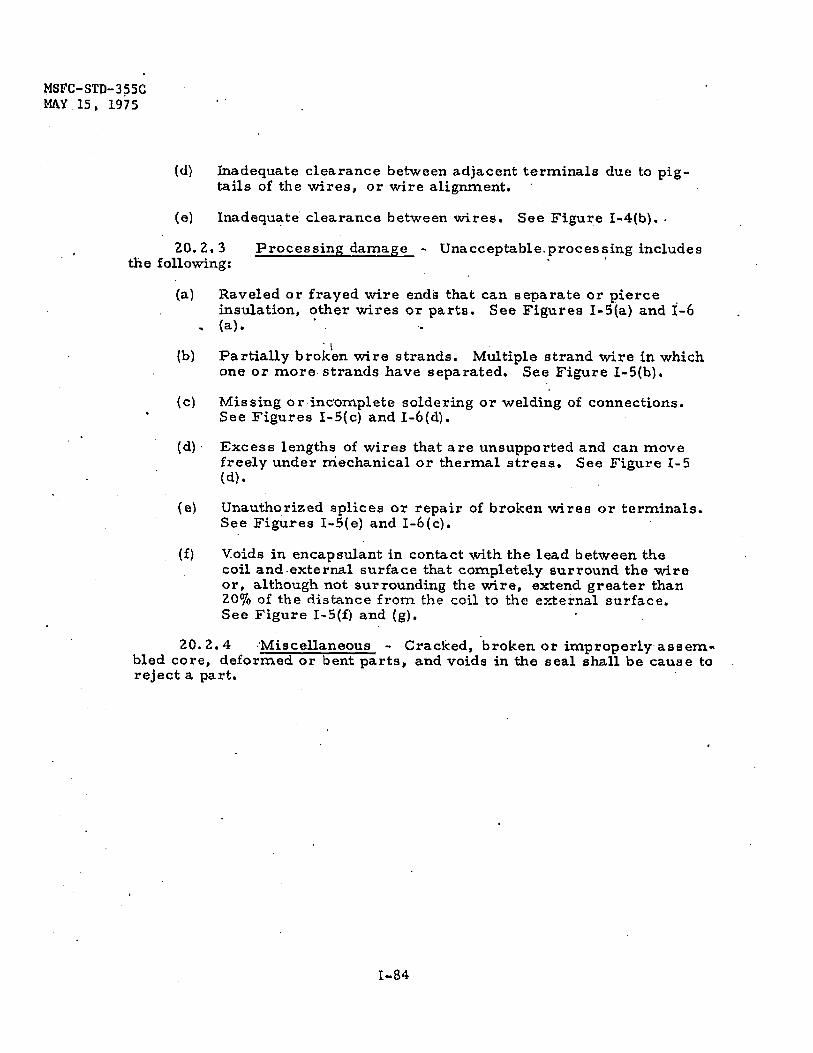
STD-355C 5, 1975
(d) Inadequate c learance between adjacent terminals due to p i g -tails of the w i r e s , or wire alignment,
(e) Inadequate c learance between w i r e s . See Figure I -4(b) . •
2 0 . 2 . 3 P r o c e s s i n g damage - Unacceptable .process ing includes the following:
(a) Raveled or frayed wire ends that can separate or pierce insulation, other wires or parts. See Figures I-5(a) and 1-6
, (a). '
(b) Part ia l ly broken wire strands. Multiple strand wire in which one o r m o r e strands have separated. See Figure I-5(b)•
(c) Miss ing o r incomplete soldering o r welding of connect ions. See F igures I -5 ( c ) and I -6(d) .
(d) E x c e s s lengths of wires that are unsupported and can move f r e e l y under mechanical o r thermal s t r e s s . See Figure 1-5 (d).
(e) Unauthorized spl i ces o r repair of broken wires o r terminals . See F igures I -5(e) and I -6 ( c ) .
(f) Voids in encapsulant in contact with the lead between the co i l and-external surface that complete ly surround the w i r e o r , although not surrounding the wi re , extend greater than 20% of the distance f r o m the coi l to the external sur face . See F igure I -5( f ) and (g). -
2 0 . 2 . 4 "Miscellaneous - Cracked, broken o r improper ly a s s e m -bled c o r e , de formed o r bent parts , and voids in the seal shall be cause to re jec t a part.
1-84
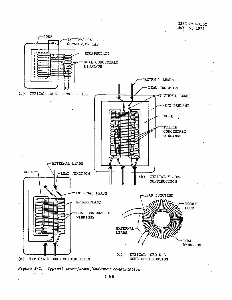
MSFC-STD-355C MAY 15, 1975
-CORE INTERNAL-EXTERNAL CONNECTION TAB
EXCAPSULANT
DUAL CONCENTRIC WINDINGS
(a) TYPICAL POWER CONSTRUCTION
EXTERNAL LEADS
LEAD JUNCTION
•EXTERNAL LEADS
LEAD JUNCTION
INTERNAL LEADS
ENCAPSULANT
CORE
TRIPLE CONCENTRIC WINDINGS
INTERNAL LEADS
ENCAPSULANT
DUAL CONCENTRIC WINDINGS
TYPICAL E-CORE CONSTRUCTION
LEAD JUNCTION
TOROID CORE
(c ) TYPICAL D-CORE CONSTRUCTION
EXTERNAL LEADS
(d) TYPICAL TOROIDAL CORE CONSTRUCTION
DUAL WINDINGS
Figure 1-1. Typical trans former/inductor construction
1-85
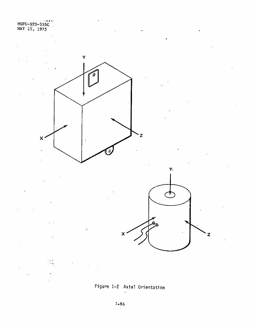
MSFC-STD-355C MAY 15, 1975
Y
1-86

MSFC-STD-355C MAY 15, 1975
SOLDER BALL REDUCING CONDUCTOR SPACING BY > 20%
SOLDER BALL > 0.254 MM (0.010 IN.) WITHIN 3.175 MM (0.125 IN.) OF CONDUCTOR
EXCESS SOLDER INCREASING JUNCTION DIAMETER > 150%
WIRE PARTICLE > 0.254 MM (0.010 IN.) LENGTH
WIRE PARTICLE WITHIN COIL
Figure J-3. Unacceptable extraneous material
(a) SPLICE TO TOP SURFACE< 3.175 MM <0.125 IN.) (b) SPLICE TO SPLICE OR WIRE-TO-WIRE SEPARATION
1.524 MM (0.06 IN.) N (c ) SPLICE OR WIRE-TO-CORE < 1.524 MM (0.06 IN.)
(d) WIRE OR SPLICE TO CONDUCTIVE CASE OR EXTERNAL SURFACE < 1.524 MM (0.06 IN.) AT SIDE
L—(e) WINDINGS TO CONDUCTIVE CASE OR EXTERNAL f SURFACE < 0.254 MM (0.010 IN.)
( f ) LEADWIRE DOES NOT CONTAIN STRESS RELIEF LOOP OR BEND 5 TO 7x DIA
Figure 1-4. Unacceptable alignment and clearances
1-87

MSFC-STD-355C tfAY 15, 1975
(a) FRAYED WIRE STRAND < 1.524 MM (0.06 IN.) FROM CORE
BREAK OF ONE OR MORE STRANDS OF MULTI-STRAND WIRE
(c) MISSING'OR INCOMPLETE SOLDER CONNECTION
(d) EXCESSIVE LOOP (LENGTH IS NOT ENCAPSULATED)
( e ) UNAUTHORIZED SPLICED WIRE
( f ) VOID SURROUNDING COIL-TO-CASE WIRE
(g) VOID > 20% OF COIL-TO-CASE LEAD LENGTH
Figure 1-5. Unaooeptable processing
I-88

MSFC-STD-35 5 C MAY 15, 1975
EXCESS SOLDER AT SPLICE INCREASING JUNCTION DIAMETER > 150%
UNAUTHORIZED WIRE SPLICE
FRAYED WIRE AT SPLICE
MISSING OR INCOMPLETE SOLDER SPLICE
WIRE PARTICLE WITHIN COIL
faQUAe 1-6 . Unacceptable. ptioce*6lng damage-toKoLdaJL con.e
1-89

MSFC-STD-355C M A Y 1 5 , 1 9 7 5 '
A P P E N D I X J
THERMISTORS
10. SCOPE
10, 1 This appendix establ ishes the m i n i m u m cr i ter ia f o r a c c e p -tance and re jec t ion of t h e r m i s t o r s supplied under the prov is ions of this standard.
20. REQUIREMENTS
1 Views - Radiographs shall be taken of each thermistor in the X and Y axes . When inadequate c o v e r a g e is prov ided , additional views shall be taken as deemed n e c e s s a r y to sat is fy the cr i ter ia defined herein .
20, 2 Examination - The radiographic examination shall include, but not be l imited to, inspect ion f o r extraneous m a t e r i a l s , parts al ignment, c l earances , p r o p e r bonds, and general workmanship . Spec i f i c detailed cr i ter ia wil l be dependent upon the configuration of the part type se lec ted .
J-91

MSFC-STD-355C MAY 15, 1975
APPENDIX K
HYBRID INTEGRATED CIRCUITS
10. SCOPE
10.1 This appendix establishes the criteria for acceptance and rejection of hybrid integrated circuits supplied under the provisions of * this standard.
20. REQUIREMENTS
1 Views - Three views shall be taken. One view shall'bo taken with the X-rays penetrating the case normal to the.plane of the substrate. A second view shall be taken with the X-rays penetrating a side. The third X-ray shall penetrate a side rotated 90 degrees from the side of the second view.
20 .2 Examination - The radiographic examination shall include,' but not be limited to, inspection for extraneous material, solder or weld splash, proper lead alignment, uniform semiconductor element and substrate bonding, and sufficient seal area.
<
20 .2 . 1 External lead alignment - The metal and glass type package shall have all leads centrally located in the glass windows. A lead within one lead wire radius of the metal package shall be cause for rejection. Ceramic packages with ribbon leads shall be rejected if any
'2 leads have less tha'n one lead width separation. Sec views (a) and (b) of Figure K - l .
20. 2. 2 • Internal lead wire - No ball bond shall bNe within 0. 0254 mm (0. 001 in.) of another ball bond. No portion o*f a lead wire, shall be within four wire diameters of another lead wire nor shall any portion of the lead wire be within 0. 1016 mm (0. 004 in.) of the case. See views (c) and (d) of Figure K - l .
20. 2. 3 Extraneous material - There shall be no visible extra-neous material. Loose or excessive bonding material, weld or solder splash, and wire particles shall be considered extraneous materials, also lead wire ends extending greater than three wire diameters beyond . a bonding point.
2 0 . 2 . 2 . 1 Excessive bonding material - Semiconductor die bonding material shall be considered excessive if the thickness at the , edge of the die exceeds the height of the top of the element. Material not touching the die shall be considered excessive if the thickness exceeds twice the die height, or is of the form shown in Figure K- l (e) .
K-93

-355C 1976
20 .2 .4 Unacceptable construction - Unacceptable construction shall include, but not be limited to, the following:
20. 2. 4, 1 Chip attach voids - Contact area voids in excess of 25 percent of the area under the chip bond area or a single void ex-tending the full length or width of the chip element bonding area. See view (f) of Figure K - l .
20. 2, 4 .2 Extraneous wire bonds - A wire bond on a semi-conductor die or substrate pad, not a portion of an interconnecting wire (rebond) shall be considered extraneous. See view (g) of Figure K - l ,
20 .2 .4 . 3 Extraneous wires - A wire bond at one or both ends, not required in the function of the circuit and not a designed test point shall be considered extraneous. See view (g) of Figure K - l .
2 0 . 2 . 3 . 4 Substrate attach voids - Contact area voids in ex-cess of 50 percent of the area under the substrate or a single void extending the full length or width of the substrate. See view (h) of Figure K - l .
2 0 . 2 . 4 . 5 Incomplete lid seal - Lid seal area in which solder covers less than 75 percent of the thickness of the wall. See view (i) of Figure K - l .
i
K-94

MSFC-STD-355C MAY 15, 1975
® ® © OFF CENTER LEAD
< LEADWIDTH OF SEPARATION
(a) METAL-GLASS PKG
< 0.1016 MM (0.004 IN.) TO CASE
( O
A HEIGHT 2X DIE HEIGHT PEDESTAL
SHAPE BUILDUP
A ^
(e)
or
A HEIGHT EXCEEDS DIE HEIGHT
(b) CERAMIC PACKAGE S LEAD SEPARATION LESS THAN 4 WIRE DIAMETERS
<d)
VOID > 25% VOID EXTENDING OF AREA EDGE TO EDGE
( f ) CHIP-
(8)
EXTRANEOUS WIRE BOND
EXTRANEOUS WIRE
SEAL LESS THAN 75% OF WIDTH
f VOID > 50% OF AREA
z VOID EXTENDING EDGE TO EDGE
(h) SUBSTRATE
/•'/./mv K-l. Unacceptable workmanship for hybrid integrated circuits
K-95

MSFC-STD-355C MAY 15, 1975
APPENDIX L
CIRCUIT BREAKERS
10. SCOPE
10. 1 This appendix establ ishes the cr i ter ia f o r acceptance and re ject ion of c i r cu i t b reakers supplied under the prov i s i ons of this standard.
20. REQUIREMENTS
20. 1 Views - Radiographs shall be taken of each device in the X and Z axes , shown in F igure L - l , as f o l l ows :
20. 1. 1 Side v iews (X axis) with the b r e a k e r in the open and c losed pos i t ions , with the locating pin o r lug on the le f t .
20. 1 .2 Edge v iew (Z axis) with the breaker in either posit ion. '
20. 2 Examination - The radiographic examination shall include, but not be l imited to inspect ion f o r extraneous fnaterial , improper o r incomplete bonds, misa l igned o r bent e lements , inadequate c l earances , i m p r o p e r w i r e terminations and incomple te a s s e m b l y . «
2 0 . 2 . 1 Extraneous mater ia l - Extraneous mater ia l shall include l o o s e or e x c e s s i v e bonding mater ia l such as weld and' so lder splash, w i re tr immings and other meta l l i c par t i c l e s . Attached bonding mater ia l i s acccptab le prov ided it mee ts the dimensional requirements of F igure L - 2 ( a ) . Examples of unacceptable extraneous mater ia l a r e shown in Figure L ' -2(b) .
2 0 . 2 . 2 Improper or incomplete bonds - Improper o r incomplete bonds shall include the fo l lowing : a) absence of bond evidence where required by design, b) w i r e attached at a point not spec i f ied in design nor common to the lot , and c) sur faces (as shown in F igure L - 3 ) attached in only a port ion of the intended a r e a .
2 0 . 2 . 3 Misal igned o r bent e lements - Movable contacts m i s -aligned to the extent that al lows the e f f e c t ive contact area to be l e s s than 90 percent of the total contact pad (X axis) a r e unacceptable . Seie Figure L - 4 ( a ) . No internal e lements shall be bent m o r e than 15 f r o m the designed conf iguration. See F igure L - 4 ( b ) .
2*0.2.4 Inadequate c l earance - The min imum c learance between pigtails and the c a s e o r other e l e c t r i ca l ly conductive e lements shall be 1 .6 m m or 0. 062 inch. See F igure L - 5 ( a ) . In addition, all w i r e s shall have adequate c l e a r a n c e to avoid contact with moving parts . See F igure L -5 (b ) .
L - 9 7

t
MSFC-STD-355C ' MAY 15, 1975
2 0 . 2 . 5 Incomplete a s s e m b l y - Incomplete assembly inspect ion cr i ter ia shall include s c rews and pins not fully inserted and seal areas containing vo ids .
2 0 . 2 . 6 Physica l damage - T h e r e shall be no vis ible c racks or f rac tures of the case mater ia l o r any internal e lements.
L -98

MSFC-STD-355C MAY 15, 1975 '
Y
(a) MANUAL RESET
Figure L-2. Circuit breaker axes
L-99
Y
(b) ELECTRICAL RESET

MSFC-STD-355C MAY 15, 1975 '
UNACCEPTABLE - PARTICLE IN CONTACT AREA
ACCEPTABLE - EXCESS MATERIAL CLEARANCE > 1.6 MM (0.0625 IN.)
VJ/// / / / / / / / / / / / / / / / r LENGTH < 1 . 6 MM (0.0625 IN.)
(a)
ACCEPTABLE ATTACHED SOLDER OR WELD SPLASH ^ t f T ^ - l
(b)
UNACCEPTABLE, LOOSE METALLIC PARTICLES > 0 . 2 5 MM (0.010 IN.)
Figure L-2> Extraneous material
L-100

MSFC-STD-3S5C MAY 15, 1975
UNACCEPTABLE INCOMPLETE HEADER TO FRAME BOND
Figure L-3. Improper/incomplete bonding
UNACCEPTABLE ACCEPTABLE BEND CONTACT OVERLAP PER DESIGN IS LESS THAN 90%
I j ? (a) (b)
TT
>151
UNACCEPTABLE BEND > 15® FROM INTENDED DESIGN
Figure*L~4t Misaligned or bent elements
L-101

MSFC-STD-355C M A Y 1 5 , 1975
UNACCEPTABLE CLEARANCE UNACCEPTABLE INADEQUATE IS LESS THAN 1.6 mm (0.0625 l a . ) CLEARANCE BETWEEN WIRE & AND WIRE HAS FRAYED END MOVABLE CORE
(a) (b)
Figure L-5, Inadequate clearance
L - 1 0 2
MSFC-STD-355C MAY 15, 1975 '
A P P E N D I X M
CRYSTALS
10. SCOPE
10. 1 This appendix establ ishes the min imum cr i ter ia f o r a c c e p -tance and re jec t ion of c rys ta l s supplied under the prov is ions of this standard.
20. REQUIREMENTS
20. 1 Views A min imum of two views shall be taken, one normal to the plane passing through the crysta l leads and one at 90 d e g r e e s f r o m the f i r s t . When two v iews prov ide inadequate c o v e r a g e , additional v iews as deemed n e c e s s a r y by the testing laboratory o r by the procur ing act iv i ty representat ive shall be required .
2 0 . 2 Examination - The radiographic examination shall inc lude, but not be l imited to, inspect ion f o r extraneous mater ia l within the enc losure , misa l igned o r mispos i t i oned c rys ta l s , leads o r tabs, phys ica l damage to any e l e c t r i ca l e lements , and i m p r o p e r internal bonds.
20. 2. 1 Extraneous mater ia l - There shall be no l o o s e o r attached extraneous mater ia l 0. 127 m i l l i m e t e r (0 .005 in . ) or l a r g e r with-in the enc losure . Part i cu lar attention shall be given to all so ldered o r welded junctions within the enc l o sure . Weld o r so lder splatter, e x c e s s so lder , o r extra tabs shall be cause f o r re ject ion (See F igure M - l ) .
20. 2. 2 Misal igned elements - Except where spec i f i ca l l y f o r m e d to hold the c rys ta l , no internal leads or tabs shall be d e f o r m e d greater than 15^ f r o m a straight l ine , hor shall the crysta l al ignment bo greater than 20 f r o m the designed ver t i ca l (or horizontal) position (See F i g u r e M - 2 ) .
2 0 . 2 . 3 Phys i ca l damage - T h e r e shall be no evidence of cuts o r nicks on the internal meta l w i r e s o r tabs (See F igure M - 3 ) ,
2 0 . 2 . 4 Improper bonds - Internal w i r e bonds shall be inspected to ensure p r o p e r overlapping of jo inted m a t e r i a l s . Insufficient o r e x c e s s -ive over lapping, beyond n o r m a l des ign shall be cause f o r re j e c t i on . In addition, the t a b - t o - c r y s t a l attachment shall be inspected f o r e x c e s s i v e mater ia l (See F i g u r e M - 4 ) .
20. 2. 5 Clearanee - Accep tab l e crysta ls shall exhibit adequate internal c l e a r a n c e . The m i n i m u m acceptab le distance between-any internal conductive e lement and a metal c a s e header o r unused pin shall be 0. 508 m i l l i m e t e r (0. 02 i n . ) .
•,M-103

15, 1975
EXCESS WELD MATERIAL > 0.127 MM (0.005 IN.) LEADS DEFORMED > 15°
EXCESS SOLDER MATERIAL
Figure M-l. Unacceptable extraneous material
A . UNACCEPTABLE
Figure M-2. Misaligned elements
INCOMPLETE TRIMMING OF TAB
CUT OR NICKED WIRE POST
Figure M-3. Unacceptable physical damage
INADEQUATE OVERLAP
EXCESS OVERLAP
Figure M-4. Improper bonds i i
M-104

George C. Marshall Space Flight Center National Aeronautics and Space Administration
STANDARD
RADIOGRAPHIC INSPECTION OF ELECTRONIC PARTS
This amendment forms a part of MSFC-STD-355C, dated 15 Nfe^ 1975.
Page C - 4 0
20 .2 .4 , add the following new paragraph:
"(c) The whisker may be deformed to the extent that it touches itself if the minimum whisker clearance zone specified in figure C-2 is maintained. This criteria applies only to whiskers metallurgically bonded to the post and to the die. n
Preparing Activity: EC43
NASA—MSFC—C :
MSFC-STD-355C Amendment 1 8 June 1977

MSFC-STD-355C Amendment 1 8 June 1977
George C, Marshall Space Flight Center National Aeronautics and Space Administration
STANDARD
RADIOGRAPHIC INSPECTION OF ELECTRONIC PARTS
This amendment forms a part of MSFC-STD-355C, dated 15 May, 1975.
Page C-40
20. 2. 4, add the following new paragraph:
"(c) The whisker may be deformed to the extent that it touches itself if the minimum whisker clearance zone specified in figure C-2 is maintained. This criteria applies only to whiskers metallurgically bonded to the post and to the die. "
Preparing Activity: EC43

MSFC-STD-355C AMENDMENT ' . 2 February 19, 1982 AMENDING MSFC-STD-355C May 15, 1975
GEORGE C. MARSHALL SPACE FLIGHT CENTER
NATIONAL AERONAUTICS AND SPACE ADMINISTRATION
STANDARD
RADIOGRAPHIC INSPECTION OF ELECTRONIC PARTS
This amendment forms a part of George C. Marshall Space Flight Center(MSFC) Standard MSFC-STD-355C, May 15, 1975, and has been approved by MSFC and is available for use by MSFC and associated nontr-'ctors.
(1) Page 2, paragraph 4.2.2(b); revise to read as follows:
"(b) H and D film density - 1.0 to 3.0"
(2) Page 2, paragraph 4.2.3; delete and substitute:
"4.2.3 Film The x-ray film shall be very fine grain single emulsion or equivalent that will permit compliance with this standard.
Notet Single emulsion very fine grain film can provide a higher degree of sensitivity, definition and contrast and thus should be considered for use when performing failure investi-gations or other hardware off-line diagnostics."
Custodian:
NASA - George C. Marshall Space Flight Center
Preparing activity:
George C. Marshall Space Flight Center

wx> • 1. DATE: :
C O N C U R R E N C E S H E E T , CONTINUED March 30, 1982 •
SUBJECT (Or brief description):
.' ' / • • Amendment to MSFC-STD-355C, dated February 19, 1982
3, ADDRESSED TO:
4. NAME OF ORIGINATING DIVISION OR OFFICE:
5. APPROVAL OF DIRECTOR, CHIEF OR AUTHORIZED REPRESENTATIVE:
E lec t ron ic Parts V e r i f i c a t i o n Branch> 3-4562
\ i
\ •
Signature and Dale
CONCURRENCES:
DIVISION OR OFFICE SIGNATURES pmeeTOR, CHIEF OR
JTHORJZEBTREPRESENTATIVE DATE
*
E H 1 1 Raymond L/Ta£use
EH02 * ' Carlo F. /C£y
EH01 . ers
EH01 7 Robert Schwteu*trSff
»
7. REMARKS/COMMENTS:
PLEASE RETURN CONCURRENCE SHEET TO EC43.
«arc • rom 1407 (F.brwf IP63) • (INSTRUCTIONS OFT REVERSE SIDE)

» 1. DATE: ' f ^ C O N C U R R E K C E S H E E T March 30, 1982
' f
SUBJECT (Or brief description); / • • •
Amendment to MSFC-STD-355C, dated February 19, 1982. •
•
3. ADDRESSED TO:
4. NAME OF ORIGINATING DIVISION OR OFFICE AND PHONE NO/.
Electronic Pants Veri f icat ion Branch. 3-4562
5. APPROVAL OF DIRECTOR, CHIEF OR AUTHORIZED REPRESENTATIVE
1 '
- 1
Signature and Date
CONCURRENCES;
DIVISION OR OFFICE
EC43
EC43
EC43
EC41
ECOl
EH13
SIGNATURE OF DIRECTOR, CHIEF IR AUTHORIZED REPRESENTATIVE
<Jj~t Bill Corder
(t F . ^ / l n e l l a
eon Harm ten. if"
John M. Gould
re^.Si Wp.itali'
L M. Knadler
DATE
Z/Zo/W*
7. REMARKS/COMMENTS:
i
MSrC • Form 140? Januw'y 1965) (INSTRVCTIONS ON KSYRXSX StDB)

MSFC DOCUMENTATION REPOSITORY - DOCUMENT INPUT RECORD I. GENERAL INFORMATION
1. APPROVED PROJECT:
M u l t i - p r o g r a m p r o j e c t s
2. DOCUMENT/ DRAWING NUMBER:
M S F C - S T D - 3 5 5 R e v i s i o n C
3. CONTROL NUMBER: 4. RELEASE DATE:
0 5 / 0 7 / 1 9 8 2
5. SUBMITTAL DATE:
1 0 / 0 7 / 2 0 0 2
6. DOCUMENT/DRAWING TITLE:
R a d i o g r a p h i c Inspec t i on o f E l e c t r o n i c Parts 7. REPORT TYPE:
M S F C Standard
8. CONTRACT NUMBER / PERFORMING ACTIVITY: 9. DRD NUMBER: 10. DPD/DRL/ IDRD NUMBER
11. DISPOSITION AUTHORITY (Check One): [X] Official Record - NRRS 8/12/A r - | Reference Copy - NRRS 8/5/A/3 I—I (destroy when no longer needed)
12. SUBMITTAL AUTHORITY:
Patrick D . M c M a n u s / E D 1 6 : s /ED16 ^h/t 0 1
14. SPECIAL INSTRUCTIONS:
D o c u m e n t wi l l b e ava i lab le o n the E l e c t r o n i c Master List.
/ s o d s j ^
15. CONTRACTOR/SUBMITTING ORGANIZATION, A D D R E S S AND PHONE NUMBER:
E D 16 Patrick D . M c M a n u s ( 2 5 6 ) 5 4 4 - 3 3 8 3
16. ORIGINATING NASA CENTER:
M S F C
17. OFFICE OF PRIMARY RESPONSIBILITY:
E D 16
18. PROGRAMMATIC CODE (5 DIGITS): 19. NUMBER OF PAGES: 102 II. ENGINEERING DRAWINGS
20. REVISION: 21. ENGINEERING ORDER: 22. PARTS LIST: 23. CCBD:
III. REPORTS, SPECIFICATIONS, ETC. 24. REVISION:
t
25. CHANGE: 26. VOLUME: 27. BOOK: 28. PART: 29. SECTION:
30. ISSUE: 31. ANNEX: 32. SCN: 33. DCN: 34. AMENDMENT:
35. APPENDIX: 36. ADDENDUM: 37. CCBD: 38. CODE ID: 39. IRN:
IV. EXPORT AND DISTRIBUTION RESTRICTIONS
• Privacy Act (see MW11382.1)
• Proprietary (see MPD 2210.1)
• Patent (see MPG 2220.1)
• ITAR (see MPG 2220.1)
• EAR (see MPG 2220.1)
• Other ACI (see NPG 1620.1 and MPG 1600.1)
No statutory or institutional restrictions applicable - material may be electronically distributed to user in the NASA domain
V. ORIGINATING ORGANIZATION APPROVAL 46!) SIGNATURE/DATE 40. ORG. CODE:
E D 16
41. PHONE NUMBER:
( 2 5 6 ) 5 4 4 - 3 3 8 3
42. NAME:
Patrick D . M c M a n u s
I OlolNrt I Uf\C/Urt I tz. J
VI. TO BE COMPLETED BY MSFC DOCUMENTATION REPOSITORY 44. RECEIVED BY:
^ ( X a t u t u a L O x g j 5 (RevCM:
45. DATE RECEIVED:
f O / v O 46. W O R K ORDER:
MSFC Form 2896 (RevUVIay 2002) PREVIOUS EDITIONS ARE OBSOLETE

HSFC-STD-355C (1 ) HI "HITIS^ 0DD1D1S fl
MSFC-STD-355C Amendment 1 8 June 1977
George C. Marshall Space Flight Center National Aeronautics and Space Administration
STANDARD
RADIOGRAPHIC INSPECTION OF ELECTRONIC PARTS
This amendment forms a part of MSFC-STD-355C, dated 15 May, 1975.
Page C - 4 0
2 0 . 2 . 4 , add the following new paragraph:
" (c) The whisker may be deformed to the extent that it touches itself if the minimum whisker clearance zone specified in figure C - 2 is maintained. This criteria applies only to whiskers metallurgically bonded to the post and to the die. "
Preparing Activity: EC43
S
P rovide d b y IH S Li censee=N ASA Techni c al St a n d a rds 4/9972545004, User=sampson, michael N o reproducti o n o r netwo rking perm i tted wi t h o u t l i cense from IHS Not for Resell e , 09/23/2009 07: 54: 32 M DT


![Welcome [core.ac.uk]scaling limitations in MSFC-STD-3676 9 Zonal Environment Application This environment applies here This environment applies here Large difference in acoustic environment](https://img.pdfslide.us/doc/110x75/60a86ba9487fbc65c049df67/welcome-coreacuk-scaling-limitations-in-msfc-std-3676-9-zonal-environment-application.jpg)