Embed Size (px)
Citation preview
MSE-630
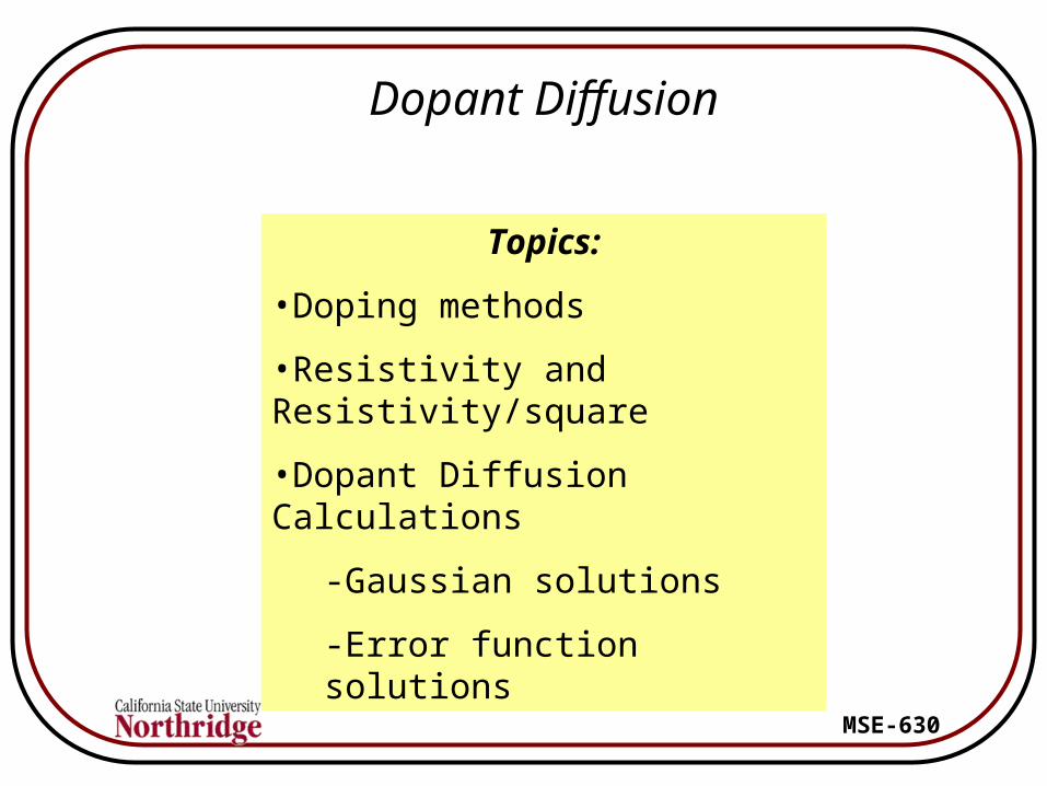
Dopant Diffusion
Topics:
•Doping methods
•Resistivity and Resistivity/square
•Dopant Diffusion Calculations
-Gaussian solutions
-Error function solutions
MSE-630
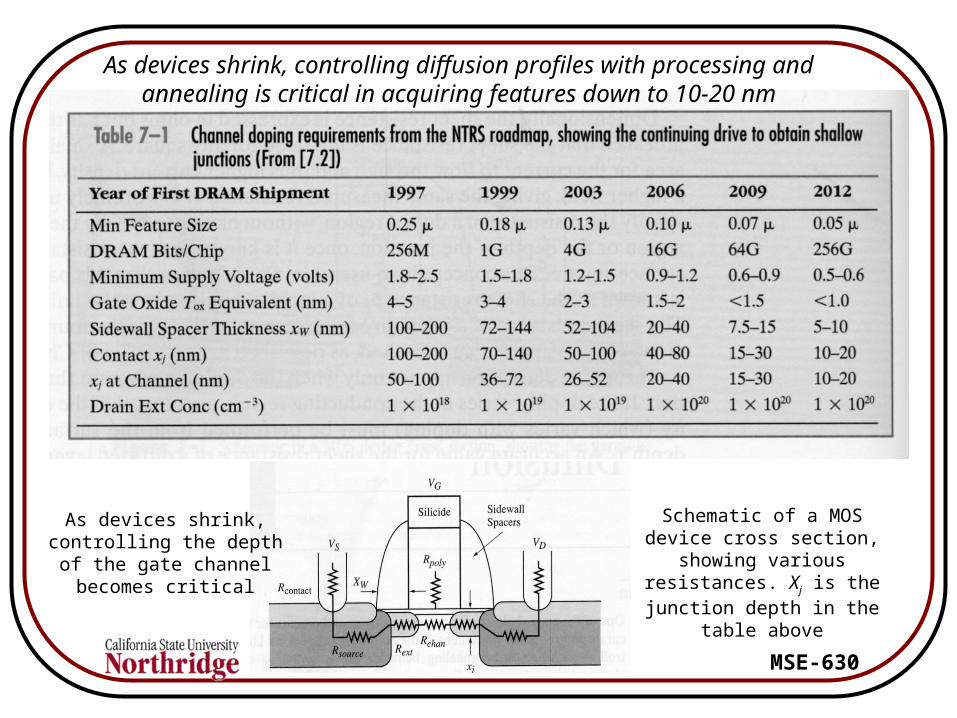
As devices shrink, controlling diffusion profiles with processing and annealing is critical in acquiring features down to 10-20 nm
Schematic of a MOS device cross section, showing various resistances. Xj is the junction
depth in the table above
As devices shrink, controlling the depth of the gate channel
becomes critical
MSE-630
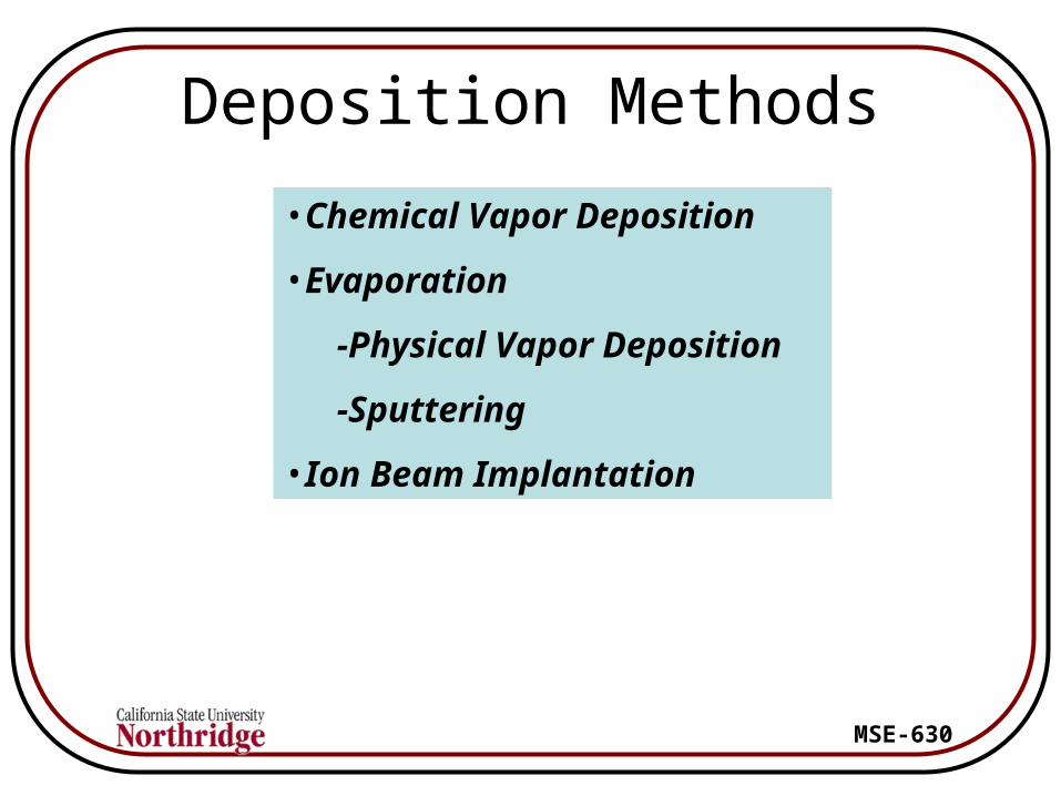
Deposition Methods
•Chemical Vapor Deposition
•Evaporation
-Physical Vapor Deposition
-Sputtering
•Ion Beam Implantation
MSE-630
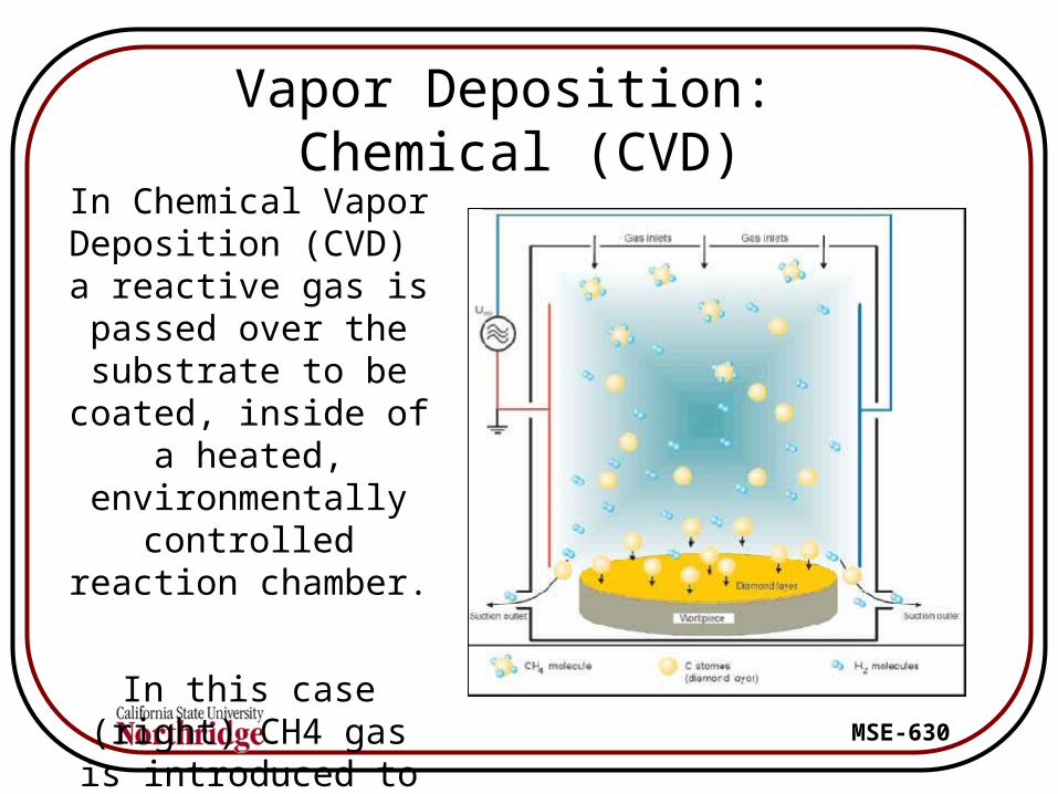
Vapor Deposition: Chemical (CVD)
In Chemical Vapor Deposition (CVD) a
reactive gas is passed over the substrate to be
coated, inside of a heated, environmentally
controlled reaction chamber.
In this case (right) CH4 gas is introduced to
create a diamond-like coating
MSE-630
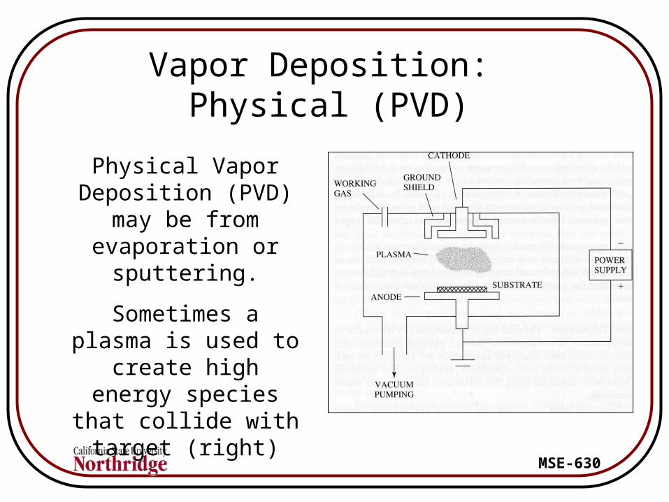
Vapor Deposition: Physical (PVD)
Physical Vapor Deposition (PVD) may be from evaporation or
sputtering.
Sometimes a plasma is used to create high energy species that
collide with target (right)
MSE-630
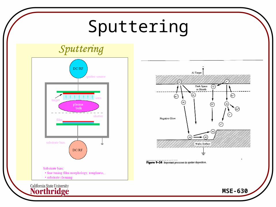
Sputtering
MSE-630
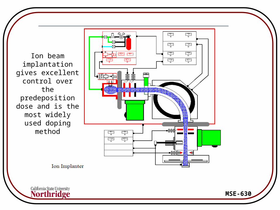
Ion beam implantation gives excellent control
over the predeposition dose
and is the most widely used doping
method
MSE-630
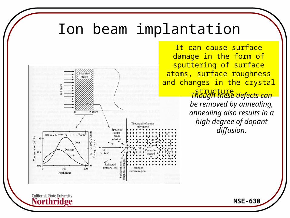
Ion beam implantationIt can cause surface damage in the form of sputtering of surface atoms, surface roughness and changes in
the crystal structure.
Though these defects can be removed by annealing, annealing also results in a
high degree of dopant diffusion.
MSE-630
MSE-630
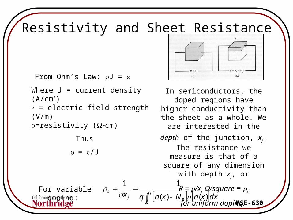
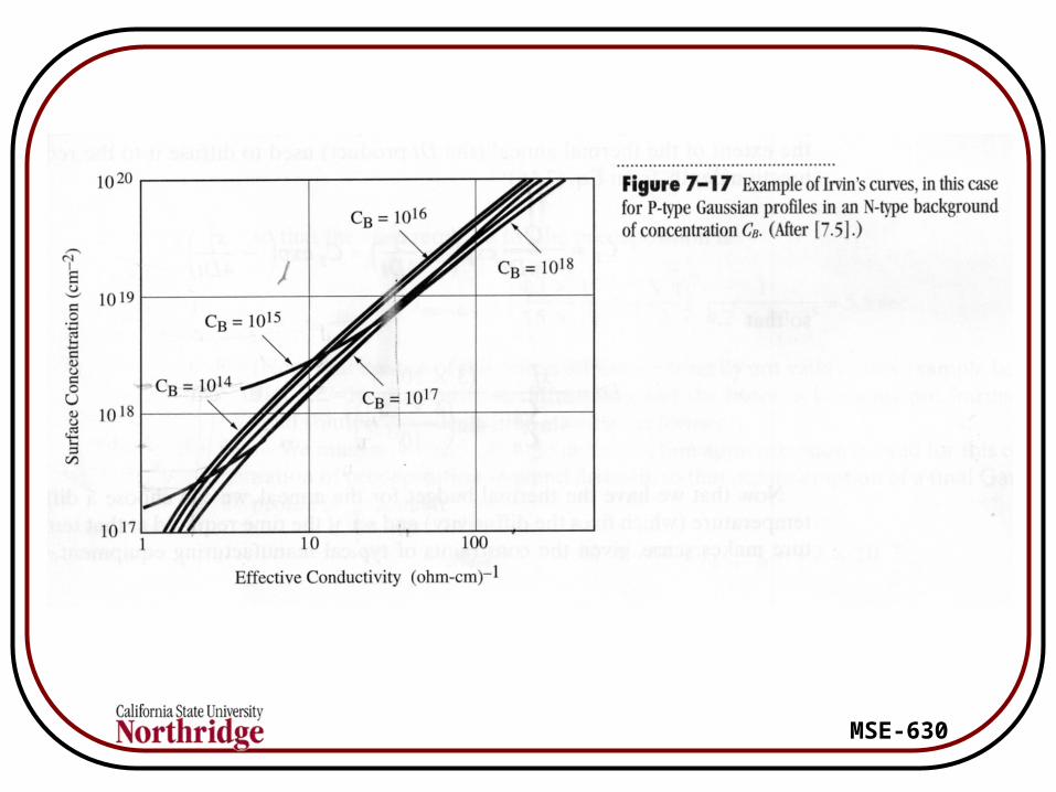
Resistivity and Sheet Resistance
From Ohm’s Law: J =
Where J = current density (A/cm2) = electric field strength (V/m)=resistivity (cm)
Thus
= /J
In semiconductors, the doped regions have higher conductivity than the sheet as a whole. We
are interested in the depth of the
junction, xj. The resistance we measure is that of a square of any dimension with depth xj, or
R = /xj /square ≡ s
for uniform doping.
For variable doping: dxxnNxnqx jx
Bjs
)()(
11
0
MSE-630
MSE-630
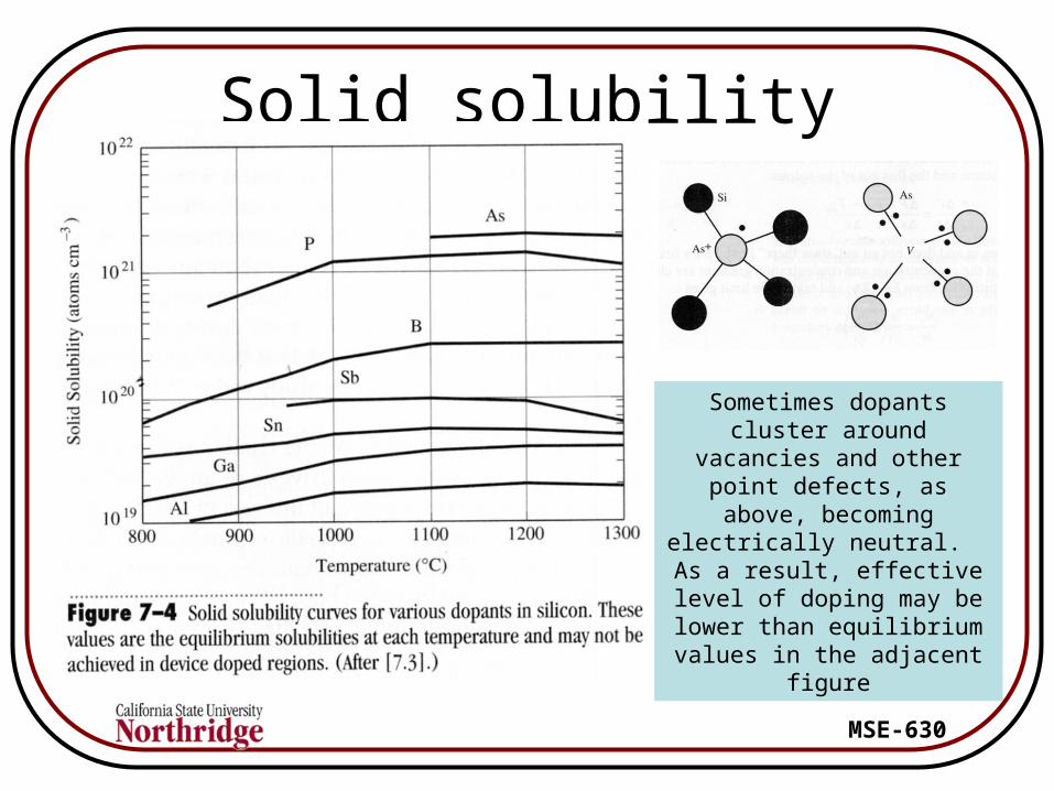
Solid solubility
Sometimes dopants cluster around vacancies and other
point defects, as above, becoming electrically neutral. As a result, effective level of doping may be lower than equilibrium values in the
adjacent figure
MSE-630
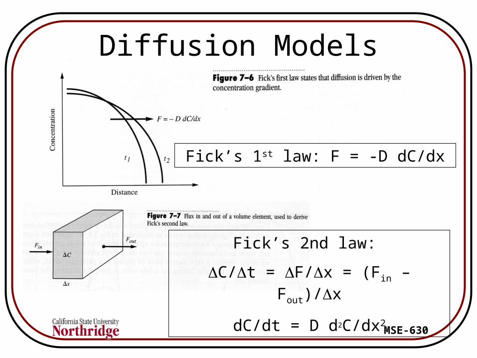
Diffusion Models
Fick’s 1st law: F = -D dC/dx
Fick’s 2nd law:
C/t = F/x = (Fin – Fout)/x
dC/dt = D d2C/dx2
MSE-630
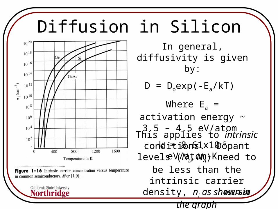
Diffusion in SiliconIn general, diffusivity is
given by:
D = Doexp(-Ea/kT)
Where Ea = activation energy ~ 3.5 – 4.5 eV/atom
k = 8.61x10⁻⁵ eV/atom-KThis applies to intrinsic
conditions. Dopant levels (ND, NA) need to be less than the intrinsic carrier density, ni
as shown in the graph
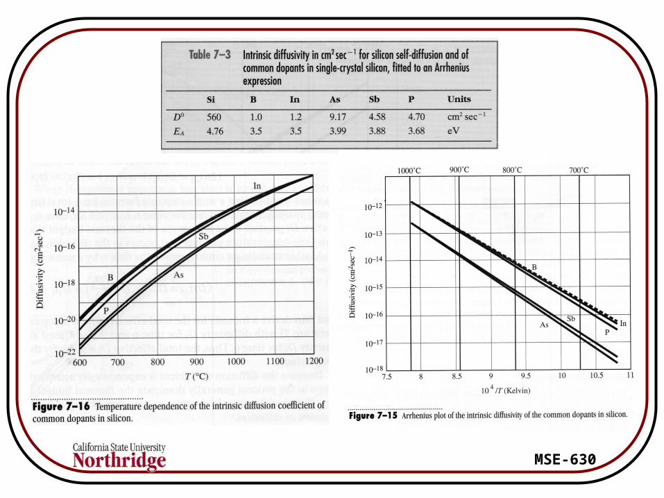
MSE-630
MSE-630
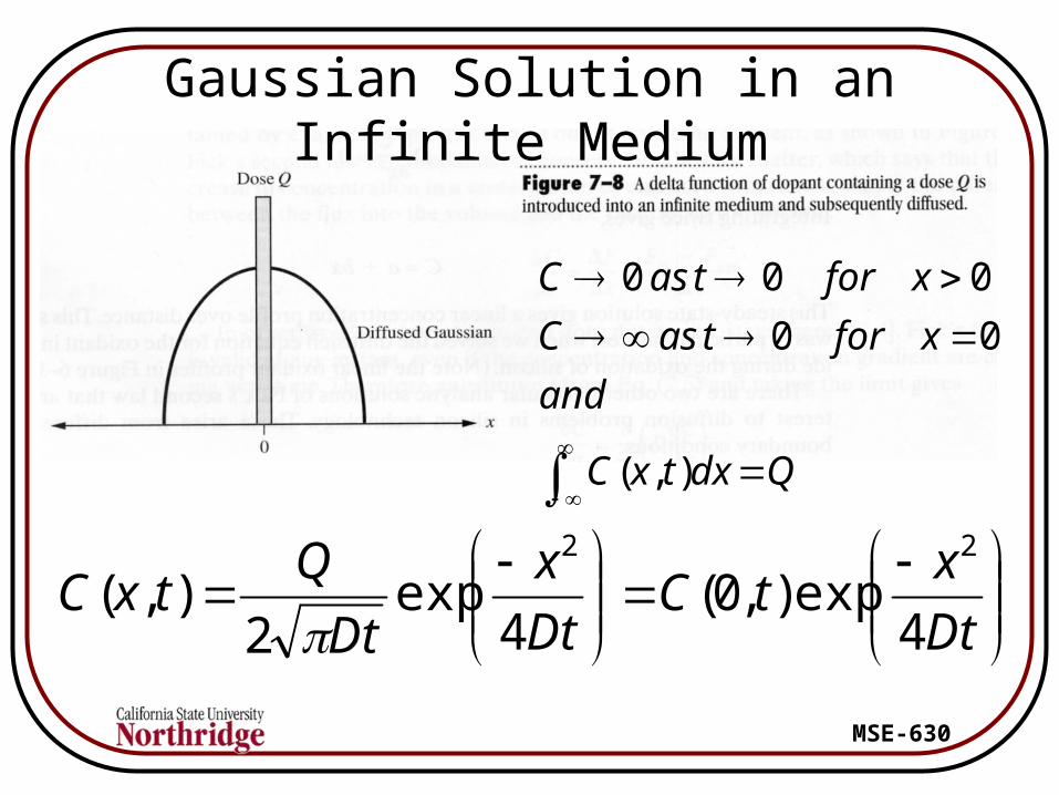
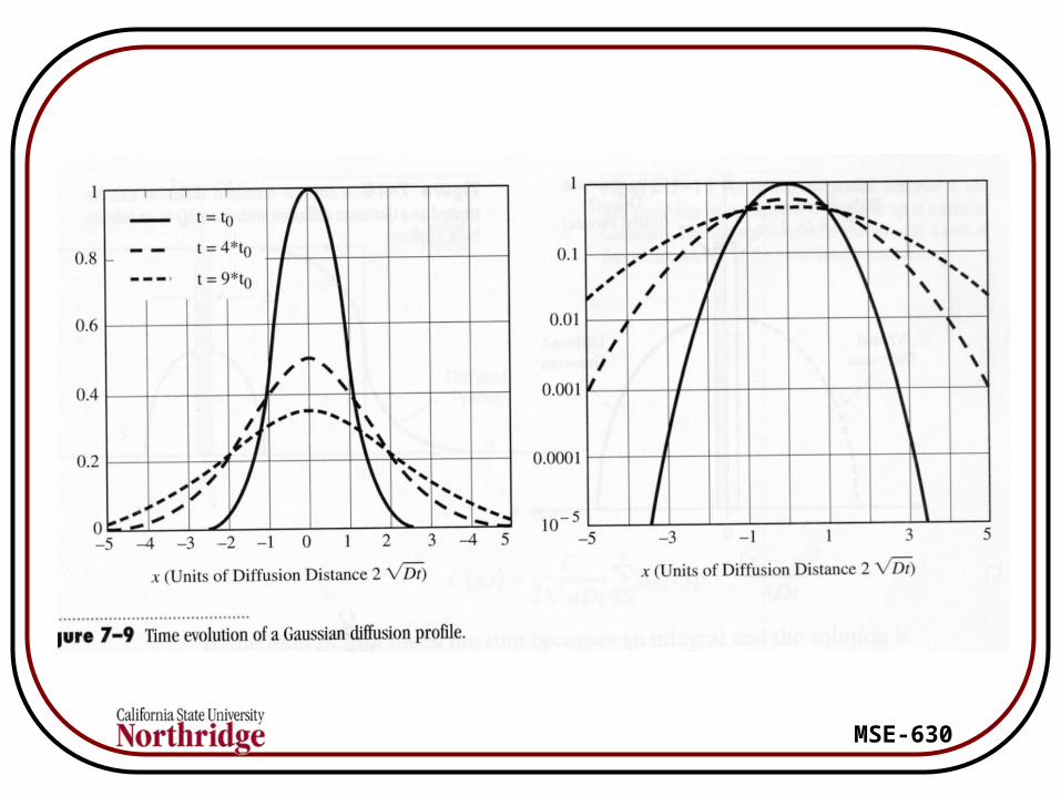
Dt
xtC
Dt
x
Dt
QtxC
4exp),0(
4exp
2),(
22
QdxtxC
and
xfortasC
xfortasC
),(
00
000
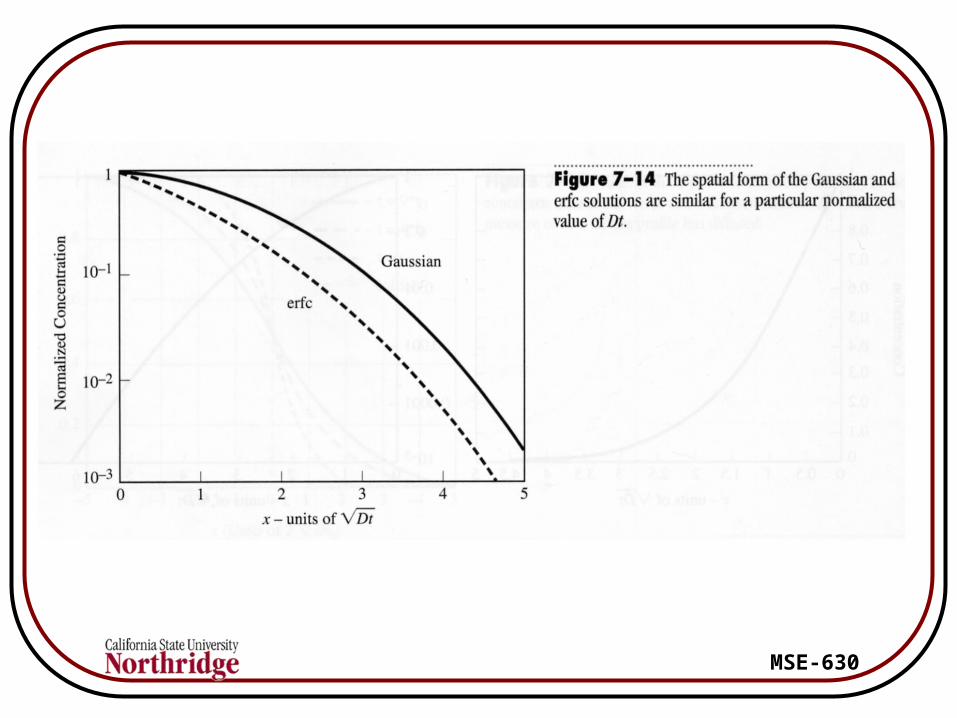
Gaussian Solution in an Infinite Medium
MSE-630
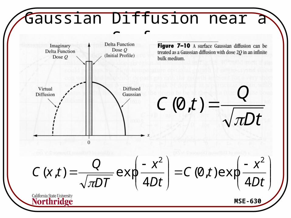
MSE-630
Gaussian Diffusion near a Surface
Dt
xtC
Dt
x
DT
QtxC
4exp),0(
4exp),(
22
Dt
QtC
),0(

MSE-630
Error-Function solution in an Infinite Medium
00
000
xfortatCC
xfortatC
Dt
xerf
CtxC
21
2),(
MSE-630
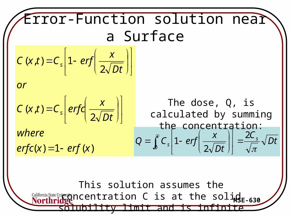
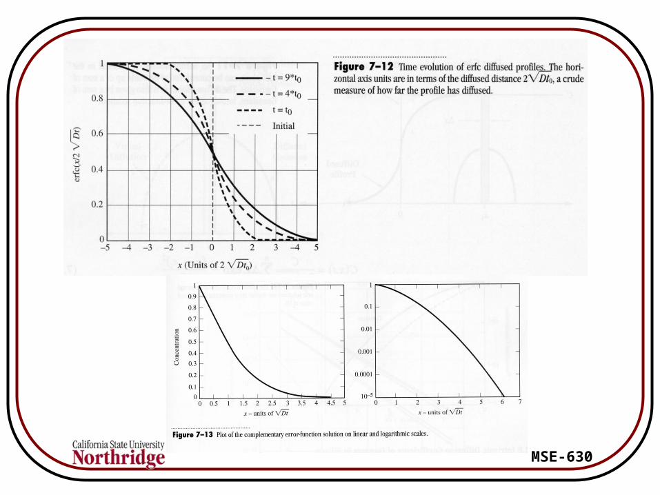
Error-Function solution near a Surface
)(1)(
2),(
21),(
xerfxerfc
where
Dt
xerfcCtxC
or
Dt
xerfCtxC
s
s
This solution assumes the concentration C is at the solid solubility limit and is infinite
DtC
Dt
xerfCQ s
s 2
21
0
The dose, Q, is calculated by summing the concentration:
MSE-630
MSE-630
MSE-630
Effect of successive diffusion steps
If diffusion occurs at constant temperature, where the diffusivity is constant, then the effective thermal budget, Dt is:
(Dt)eff = D1t1+D1t2+…D1tn
If D is not constant, then time is increased by the ratio of D2/D1, or
(Dt)eff = D1t1+D1t2(D2/D1)+…D1tn(Dn/D1)
MSE-630


![[XLS] · Web viewAnalysis and Estimation of Service Life of Corrosion Prevention Materials Using Diffusion, Resistivity and Accelerated Curing for New Bridge Structures](https://img.pdfslide.us/doc/110x75/5b4563297f8b9ad1138ba492/xls-web-viewanalysis-and-estimation-of-service-life-of-corrosion-prevention.jpg)