Embed Size (px)
Citation preview
Freescale SemiconductorApplication Note
AN2946Rev. 0, 2/2005
CONTENTS
1 TDM Basics ............................................................11.1 TDM Architecture ...................................................21.2 TDM Signals ...........................................................31.3 Clock and Frame Sync ............................................52 TDM Configuration Examples ................................72.1 DMA Channel Assignments ...................................92.2 Interleaved Versus Deinterleaved Data .................102.3 Using DMA to Interleave Data .............................112.4 Using DMA to Deinterleave Data .........................132.5 Interrupting Every n Frames .................................152.6 Using Double Buffers with Two-Channel
DMA Transfers .....................................................173 TDM Initialization ................................................214 Dynamic Channel Configuration ..........................235 System Tuning ......................................................245.1 DMA Priorities ......................................................245.2 Crossbar Switch Tuning........................................ 25
MSC711x Time-Division Multiplexing (TDM) Usage ExamplesBy Barbara Johnson
The time-division multiplexing (TDM) interface on the Freescale MSC711x devices provides full duplex, bidirectional communication over a single bus. This application note presents examples of how to multiplex data on the TDM interface and use the DMA controller to receive data from the TDM. It also discusses different ways to map the data into the DMA channels, with code examples.
1 TDM BasicsEach MSC711x DSP has one or more identical TDM modules. The number of TDM modules is device-dependent. Refer to Table 1 for the number of TDMs for each product.
Table 1. TDMs on MSC711x
Device Number of TDMs
MSC7110 1
MSC7112 2
MSC7113 2
MSC7115 3
MSC7116 2
Each TDM module has the following features:
• Independent or shared transmit and receive sections
• Independent or shared clock and frame sync
• Glueless interface to E1/T1 framers and MVIP, SCAS, and H.110 buses
© Freescale Semiconductor, Inc., 2005. All rights reserved.
TDM Basics
• Hardware A-law/µ-law conversion
• Data rates up to 50 Mbps
• Up to 128 channels
• 8- or 16-bit word width
• Programmable direction for TDM clock and frame sync
• Programmable delay of 0–3 bits between the frame sync signal and the beginning of the data
• MSB or LSB first
• Loopback mode
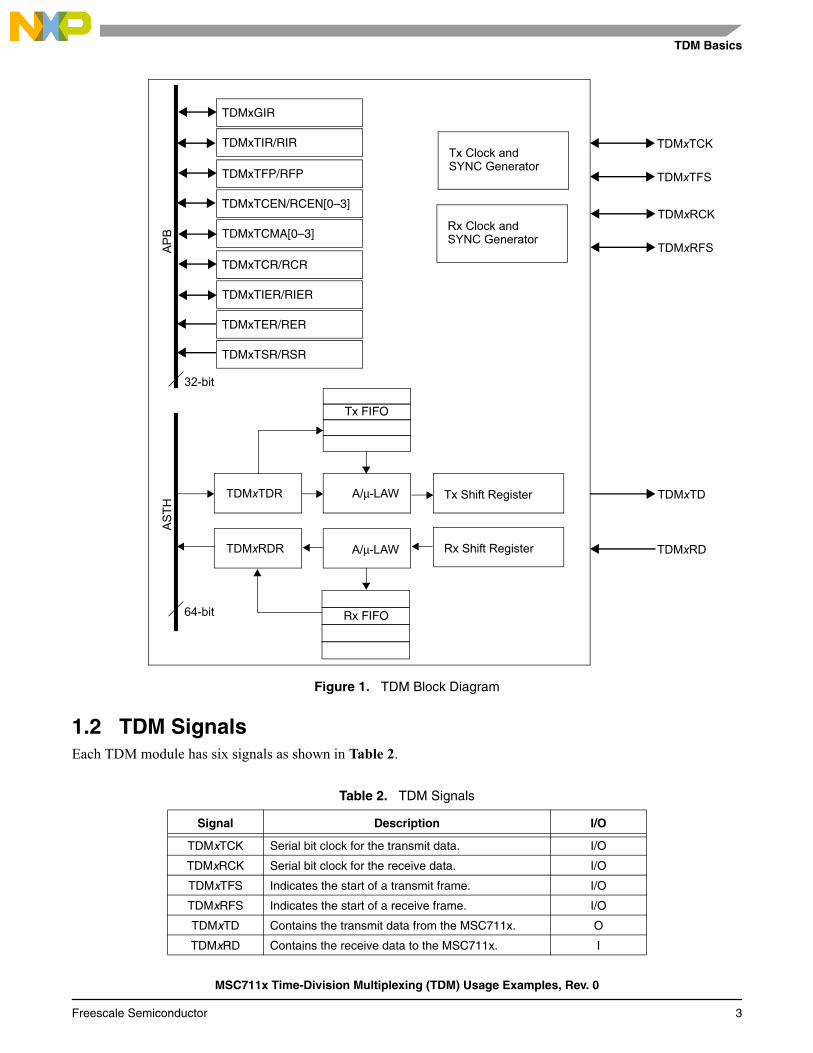
1.1 TDM ArchitectureAs the block diagram in Figure 1 shows, the TDM configuration, control, event, and status registers are accessed via the 32-bit advanced peripheral bus (APB). Data transmitted and received by the TDM is accessed on the 64-bit advanced high-speed bus slave-to-TDM/HDI16 bus (ASTH).
The TDM serial bit clock TDMxTCK/RCK signals can be internally generated from timer B or input from an external source. When the bit clock is an output, the clock and sync generator divides the bit clock by 8 or 16, depending on the channel width, to generate an internal word clock that counts the number of data bits per time slot. The word clock is then divided by the number of time slots per frame up to 128 to generate the frame sync signals on TDMxTFS/RFS.
The Transmit Data Register (TDMxTDR) holds the data to be transmitted from the MSC711x device. The 4-line deep FIFO can optionally be enabled to buffer data. An interrupt is generated according to how much data is held in the FIFO. When the FIFO is not used, the data is transferred from the TDMxTDR to the transmit shift register. When 8 bits encoded A-law are transmitted out of the TDM, the 16-bit data in the TDMxTD is composed of 13 bits of pulse code modulation (PCM) data followed by three zeros on the right. When 8 bits encoded µ-law are transmitted out of the TDM, the 16-bit data in the TDMxTDR is composed of 14 bits of PCM data followed by two zeros on the right. The hardware A-law/µ-law compander compresses the 16-bit data to 8-bit A-law/µ-law data. Data in the transmit shift register is shifted on the TDMxTD pin, one bit per rising edge of TDMxTCK.
Data on the TDMxRD pin is shifted into the receive shift register, one bit per falling edge of TDMxRCK. The length of each receive channel can be 8 bits, 8 bits encoded A-law, 8 bits encoded µ-law, or 16 bits. When the receive data is A-law encoded, the compressed data is converted into a 13-bit PCM linear sample padded with three zeros on the right to create 16-bit data. When the receive data is µ-law encoded, the compressed data is converted into a 14-bit PCM linear sample padded with two zeros on the right to create 16-bit data. The 4-line deep FIFO can optionally be enabled to buffer data. Interrupts are generated according to how much data is held in the FIFO. When the FIFO is not in use, the data in the receive shift register is transferred to the receive data register TDMxRDR after 8 or 16 bits of data are shifted in from the receive shift register.
MSC711x Time-Division Multiplexing (TDM) Usage Examples, Rev. 0
2 Freescale Semiconductor
TDM Basics
TDMxTCEN/RCEN[0–3]
TDMxTCMA[0–3]
TDMxTCR/RCR
TDMxTIER/RIER
TDMxTFP/RFP
TDMxTIR/RIR
TDMxGIR
TDMxTER/RER
TDMxTSR/RSR
Tx Clock andSYNC Generator
Rx Clock andSYNC Generator
TDMxTCK
TDMxTFS
TDMxRCK
TDMxRFSAP
B
32-bit
ASTH
64-bit
A/µ-LAW Tx Shift RegisterTDMxTDR
A/µ-LAW Rx Shift RegisterTDMxRDR
TDMxTD
TDMxRD
Tx FIFO
Rx FIFO
Figure 1. TDM Block Diagram
1.2 TDM SignalsEach TDM module has six signals as shown in Table 2.
Table 2. TDM Signals
Signal Description I/O
TDMxTCK Serial bit clock for the transmit data. I/O
TDMxRCK Serial bit clock for the receive data. I/O
TDMxTFS Indicates the start of a transmit frame. I/O
TDMxRFS Indicates the start of a receive frame. I/O
TDMxTD Contains the transmit data from the MSC711x. O
TDMxRD Contains the receive data to the MSC711x. I
MSC711x Time-Division Multiplexing (TDM) Usage Examples, Rev. 0
Freescale Semiconductor 3
TDM Basics
Table 3 shows the TDM pins and their GPIO port pin assignments. Port A contains the TDM0 and TDM1 pins. Both port A and port D contain the TDM2 pins. Four registers must be programmed to configure the port pins for TDM operation:
• Device Configuration Register (DEVCFG). Selects between the secondary and additional function of the port pins. When TDM0 and/or TDM1 is used, the Port A Select (PAS) and Port D Select (PDS) bits must be cleared to select secondary functionality. When TDM2 is used, the PAS and PDS bits must be set to select additional functionality.
• Port x Control Register (PxCTL). Configures a pin for GPIO or peripheral function. For TDM0, PACTL[11–6] must be set. For TDM1, PACTL[5–0] must be set. For TDM2, PACTL[29–27] and PDCTL[6–4] must be set.
• Port x Data Direction Register (PxDDR). Specifies whether the corresponding pin is an input or an output. For TDM operation, these bits should be cleared.
• Port x Data Register (PxDR). Indicates the value written to the GPIO pin. For TDM operation, these bits should be cleared.
Table 3. GPIO Pin Assignment for TDM
TDMx Signal Port BitSecondary/Additional Function
TDM0 TDM0RCK A 11 Secondary
TDM0RFS A 10 Secondary
TDM0RD A 9 Secondary
TDM0TCK A 8 Secondary
TDM0TFS A 7 Secondary
TDM0TD A 6 Secondary
TDM1 TDM1RCK A 5 Secondary
TDM1RFS A 4 Secondary
TDM1RD A 3 Secondary
TDM1TCK A 2 Secondary
TDM1TFS A 1 Secondary
TDM1TD A 0 Secondary
TDM2 TDM2RCK A 27 Additional
TDM2RFS D 4 Additional
TDM2RD A 28 Additional
TDM2TCK D 5 Additional
TDM2TFS A 29 Additional
TDM2TD D 6 Additional
MSC711x Time-Division Multiplexing (TDM) Usage Examples, Rev. 0
4 Freescale Semiconductor
TDM Basics
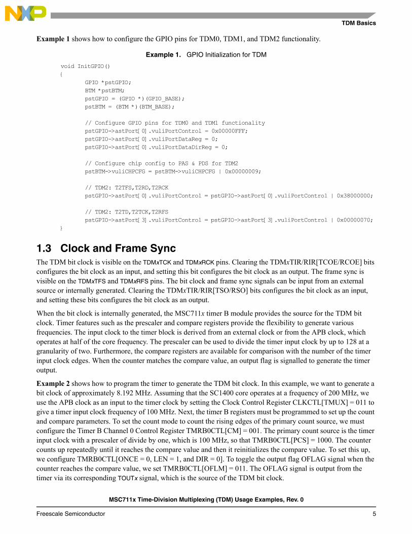
Example 1 shows how to configure the GPIO pins for TDM0, TDM1, and TDM2 functionality.
Example 1. GPIO Initialization for TDM
void InitGPIO(){
GPIO *pstGPIO;BTM *pstBTM; pstGPIO = (GPIO *)(GPIO_BASE);pstBTM = (BTM *)(BTM_BASE);
// Configure GPIO pins for TDM0 and TDM1 functionality pstGPIO->astPort[0].vuliPortControl = 0x00000FFF;
pstGPIO->astPort[0].vuliPortDataReg = 0;pstGPIO->astPort[0].vuliPortDataDirReg = 0;
// Configure chip config to PAS & PDS for TDM2pstBTM->vuliCHPCFG = pstBTM->vuliCHPCFG | 0x00000009;
// TDM2: T2TFS,T2RD,T2RCKpstGPIO->astPort[0].vuliPortControl = pstGPIO->astPort[0].vuliPortControl | 0x38000000;
// TDM2: T2TD,T2TCK,T2RFSpstGPIO->astPort[3].vuliPortControl = pstGPIO->astPort[3].vuliPortControl | 0x00000070;
}
1.3 Clock and Frame SyncThe TDM bit clock is visible on the TDMxTCK and TDMxRCK pins. Clearing the TDMxTIR/RIR[TCOE/RCOE] bits configures the bit clock as an input, and setting this bit configures the bit clock as an output. The frame sync is visible on the TDMxTFS and TDMxRFS pins. The bit clock and frame sync signals can be input from an external source or internally generated. Clearing the TDMxTIR/RIR[TSO/RSO] bits configures the bit clock as an input, and setting these bits configures the bit clock as an output.
When the bit clock is internally generated, the MSC711x timer B module provides the source for the TDM bit clock. Timer features such as the prescaler and compare registers provide the flexibility to generate various frequencies. The input clock to the timer block is derived from an external clock or from the APB clock, which operates at half of the core frequency. The prescaler can be used to divide the timer input clock by up to 128 at a granularity of two. Furthermore, the compare registers are available for comparison with the number of the timer input clock edges. When the counter matches the compare value, an output flag is signalled to generate the timer output.
Example 2 shows how to program the timer to generate the TDM bit clock. In this example, we want to generate a bit clock of approximately 8.192 MHz. Assuming that the SC1400 core operates at a frequency of 200 MHz, we use the APB clock as an input to the timer clock by setting the Clock Control Register CLKCTL[TMUX] = 011 to give a timer input clock frequency of 100 MHz. Next, the timer B registers must be programmed to set up the count and compare parameters. To set the count mode to count the rising edges of the primary count source, we must configure the Timer B Channel 0 Control Register TMRB0CTL[CM] = 001. The primary count source is the timer input clock with a prescaler of divide by one, which is 100 MHz, so that TMRB0CTL[PCS] = 1000. The counter counts up repeatedly until it reaches the compare value and then it reinitializes the compare value. To set this up, we configure TMRB0CTL[ONCE = 0, LEN = 1, and DIR = 0]. To toggle the output flag OFLAG signal when the counter reaches the compare value, we set TMRB0CTL[OFLM] = 011. The OFLAG signal is output from the timer via its corresponding TOUTx signal, which is the source of the TDM bit clock.
MSC711x Time-Division Multiplexing (TDM) Usage Examples, Rev. 0
Freescale Semiconductor 5
TDM Basics
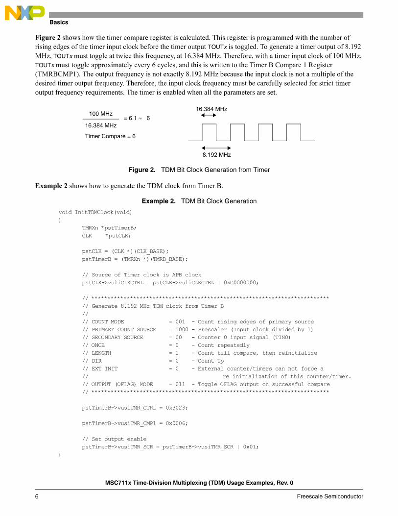
Figure 2 shows how the timer compare register is calculated. This register is programmed with the number of rising edges of the timer input clock before the timer output TOUTx is toggled. To generate a timer output of 8.192 MHz, TOUTx must toggle at twice this frequency, at 16.384 MHz. Therefore, with a timer input clock of 100 MHz, TOUTx must toggle approximately every 6 cycles, and this is written to the Timer B Compare 1 Register (TMRBCMP1). The output frequency is not exactly 8.192 MHz because the input clock is not a multiple of the desired timer output frequency. Therefore, the input clock frequency must be carefully selected for strict timer output frequency requirements. The timer is enabled when all the parameters are set.
8.192 MHz
16.384 MHz100 MHz
16.384 MHz= 6.1 ≈ 6
Timer Compare = 6
Figure 2. TDM Bit Clock Generation from Timer
Example 2 shows how to generate the TDM clock from Timer B.
Example 2. TDM Bit Clock Generation
void InitTDMClock(void){
TMRXn *pstTimerB;CLK *pstCLK;
pstCLK = (CLK *)(CLK_BASE);pstTimerB = (TMRXn *)(TMRB_BASE);
// Source of Timer clock is APB clockpstCLK->vuliCLKCTRL = pstCLK->vuliCLKCTRL | 0xC0000000;
// ************************************************************************** // Generate 8.192 MHz TDM clock from Timer B // // COUNT MODE = 001 - Count rising edges of primary source
// PRIMARY COUNT SOURCE = 1000 - Prescaler (Input clock divided by 1)// SECONDARY SOURCE = 00 - Counter 0 input signal (TIN0)
// ONCE = 0 - Count repeatedly // LENGTH = 1 - Count till compare, then reinitialize // DIR = 0 - Count Up // EXT INIT = 0 - External counter/timers can not force a
// re initialization of this counter/timer. // OUTPUT (OFLAG) MODE = 011 - Toggle OFLAG output on successful compare
// **************************************************************************
pstTimerB->vusiTMR_CTRL = 0x3023;
pstTimerB->vusiTMR_CMP1 = 0x0006;
// Set output enable pstTimerB->vusiTMR_SCR = pstTimerB->vusiTMR_SCR | 0x01;
}
MSC711x Time-Division Multiplexing (TDM) Usage Examples, Rev. 0
6 Freescale Semiconductor
TDM Configuration Examples
When the frame sync is internally generated, the TDM frame sync generator automatically generates the frame sync signal based on the bit clock, the channel size, and the number of time slots in a frame. The frame sync generator divides the bit clock by 8 or 16, depending on the width of each channel. The channel size is programmable via the TDMxTFP/RFP[TCS/RCS] bits. The output of this divider is the word clock to mark the start of each channel’s data. Next, the frame sync generator divides this word clock by the number of time slots within a frame, which can be up to 128 time slots at a granularity of two. The number of time slots within a frame is programmable in the TDMxTFP/RFP[TNCF/RNCF] bits. The output of this divider is the frame sync to mark the start of a frame. Figure 3 shows the block diagram of the frame sync generator.
TDMxTFP/RFP[TCS/RCS]8 or 16
TDMxTCK,TDMxRCK
Bit ClockChannel Size
TDMxTFP/RFP[TNCF/RNCF]1 to 128 (even)
Num of Time Slots TDMxTFS,TDMxRFS
Frame Sync
Figure 3. Frame Sync Generator
For example, if the TDM bit clock is 8.192 MHz and the TDM has 128 time slots of 8-bit data, the output frame sync frequency is calculated as follows:
8.192 MHz 8 bitschannel
128 channelsframe
÷ = 8 KHz÷
2 TDM Configuration ExamplesThis section illustrates how to program the TDM configuration and control registers for the desired frame parameters. For the example discussed here, we configure TDM0 for a 8.192 MHz bit clock and 16 active 8-bit channels. The TDM operates in internal loopback mode with the TDM0TD output internally connected to the TDM0RD input. The following registers are required to define the serial interface:
• TDM0 General Interface Register (TDM0GIR). The TDM operating mode. For internal loopback mode, we must set LPBK = 1, and the receive and transmit frame parameters must be the same. For simplicity, we configure the TDMs to share the same bit clock and frame sync by setting CTS = 1. We also configure the receive and transmit sections to share the same bit clock and sync. With these RTS and CTS settings, the TDM pin assignments are as follows:
— TDM0TCK is the shared bit clock signal between the receive and transmit sections of each TDM module.
— TDM0TFS is the shared frame sync signal between the receive and transmit sections of each TDM module.
— TDM0TD is the transmit data signal for TDM0.— TDM0RD is the receive data signal for TDM0.
• TDM0 Receive Interface Register (TDM0RIR). The receiver interface operation is configured as follows:
— Enable the FIFO and select wide mode (RFEN = 1 and RWEN = 1). — The receive FIFO full event occurs when there are one or more elements in the FIFO (RFWM =
00).
MSC711x Time-Division Multiplexing (TDM) Usage Examples, Rev. 0
Freescale Semiconductor 7
TDM Configuration Examples
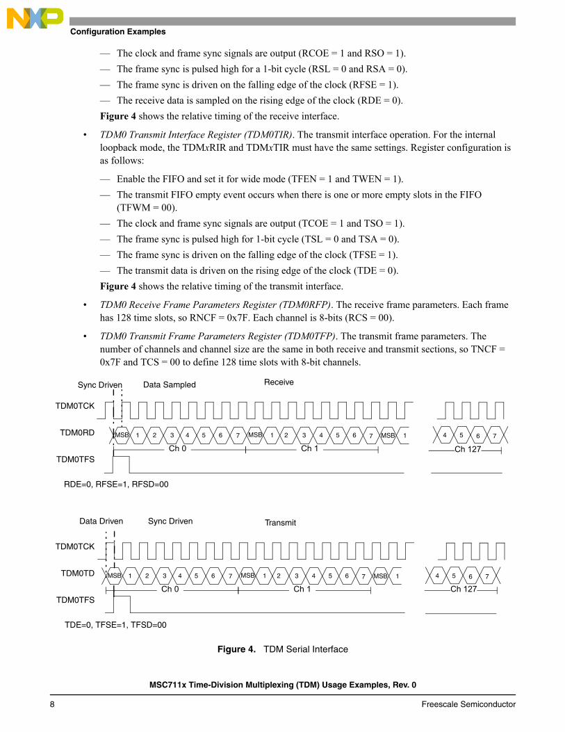
— The clock and frame sync signals are output (RCOE = 1 and RSO = 1). — The frame sync is pulsed high for a 1-bit cycle (RSL = 0 and RSA = 0). — The frame sync is driven on the falling edge of the clock (RFSE = 1). — The receive data is sampled on the rising edge of the clock (RDE = 0). Figure 4 shows the relative timing of the receive interface.
• TDM0 Transmit Interface Register (TDM0TIR). The transmit interface operation. For the internal loopback mode, the TDMxRIR and TDMxTIR must have the same settings. Register configuration is as follows:
— Enable the FIFO and set it for wide mode (TFEN = 1 and TWEN = 1). — The transmit FIFO empty event occurs when there is one or more empty slots in the FIFO
(TFWM = 00). — The clock and frame sync signals are output (TCOE = 1 and TSO = 1). — The frame sync is pulsed high for 1-bit cycle (TSL = 0 and TSA = 0). — The frame sync is driven on the falling edge of the clock (TFSE = 1). — The transmit data is driven on the rising edge of the clock (TDE = 0). Figure 4 shows the relative timing of the transmit interface.
• TDM0 Receive Frame Parameters Register (TDM0RFP). The receive frame parameters. Each frame has 128 time slots, so RNCF = 0x7F. Each channel is 8-bits (RCS = 00).
• TDM0 Transmit Frame Parameters Register (TDM0TFP). The transmit frame parameters. The number of channels and channel size are the same in both receive and transmit sections, so TNCF = 0x7F and TCS = 00 to define 128 time slots with 8-bit channels.
MSB 1 2 3 4 5 6 MSB 1 2 3 4 5 6 7TDM0RD
TDM0TCK
TDM0TFS
Receive
MSB 17
Ch 0 Ch 17654
Ch 127
RDE=0, RFSE=1, RFSD=00
TDM0TD
TDM0TCK
TDM0TFS
Transmit
Ch 0 Ch 1 Ch 127
TDE=0, TFSE=1, TFSD=00
Sync Driven Data Sampled
Sync DrivenData Driven
MSB 1 2 3 4 5 6 MSB 1 2 3 4 5 6 7 MSB 17 7654
Figure 4. TDM Serial Interface
MSC711x Time-Division Multiplexing (TDM) Usage Examples, Rev. 0
8 Freescale Semiconductor
TDM Configuration Examples
Example 3 shows the code to configure the TDM serial interface with the desired parameters.
Example 3. TDM Frame Configuration
void InitTDMParams(void){
TDM *pstTDM0;pstTDM0 = (TDM *)(TDM0_BASE);// **********************************************// Configure TDM0: // 128 time slots, 16 channels, 8-bits/channel// Loopback mode// **********************************************// TDM0 shares signals with other TDMs// Rx/Tx share same sync and clock// Loopback modepstTDM0->vuliGIR = 0x00000007;
// Rx wide FIFO enabled// Rx FIFO full with 1 element// Rx sync output, 1-bit length, active on '1'// Rx clock output// Rx DMA request when Rx FIFO full RFF=1// Rx data sampled on rising edge of clock// Rx sync sampled on falling edge of clockpstTDM0->vuliRIR = 0x0000E242;
// Tx wide FIFO enabled// Tx FIFO empty with 1 empty slots// Tx sync output, 1-bit length, active on '1'// Tx clock output// Tx DMA request when Tx FIFO empty TFE=1// Tx data driven on rising edge of clock// Tx sync driven on falling edge of clockpstTDM0->vuliTIR = 0x0000E242;
// 128 time slots, 16 channels active// 8-bits/channelpstTDM0->vuliRFP = 0x007f0000;
// 128 time slots, 16 channels active// 8-bits/channelpstTDM0->vuliTFP = 0x007f0000;
}
2.1 DMA Channel AssignmentsThe DMA can be configured to work with the TDM to transfer data in and out of the TDMxRDR and TDMxTDR. Setting the TDMxTIR/RIR[TDMA/RDMA] bits enables the TDM to request DMA service for the transmitter and the receiver. Each TDM module is assigned one DMA channel to transfer data from the TDMxTDR and another DMA channel to transfer data to the TDMxRDR. Table 4 shows the DMA channel assignments for TDM data transfers.
MSC711x Time-Division Multiplexing (TDM) Usage Examples, Rev. 0
Freescale Semiconductor 9
TDM Configuration Examples
Table 4. DMA Channel Assignments
DMA Channel TDM Assignment
0 TDM0 transmit
1 TDM0 receive
2 TDM1 transmit
3 TDM1 receive
12 TDM2 transmit
13 TDM2 receive
The examples shown in this section enable the FIFO. For TDM0, DMA channel 0 transfers data from the transmit buffer to the TDM0TDR data register when the Tx FIFO is empty, which is indicated by TDM0TER[TFE]=1 in the event register. A Tx FIFO empty event occurs when the Tx FIFO falls below the programmed watermark. All the examples assume that the Tx FIFO empty event occurs when the Tx FIFO has one or more empty slots. Similarly, DMA channel 1 transfers data from the TDM0RDR data register to the receiver buffer when the Rx FIFO is full, which is indicated by TDM0RER[RFE] = 1 in the event register. An Rx FIFO full event occurs when the Rx FIFO reaches the programmed watermark. All the examples assume that the Rx FIFO full event occurs when the Rx FIFO has one or more elements.
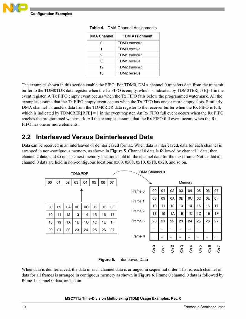
2.2 Interleaved Versus Deinterleaved DataData can be received in an interleaved or deinterleaved format. When data is interleaved, data for each channel is arranged in non-contiguous memory, as shown in Figure 5. Channel 0 data is followed by channel 1 data, then channel 2 data, and so on. The next memory locations hold all the channel data for the next frame. Notice that all channel 0 data are held in non-contiguous locations 0x00, 0x08, 0x10, 0x18, 0x20, and so on.
00 01 02 03 04 05 06 07
TDMxRDR
08 09 0A 0B 0C 0D 0E 0F
10 11 12 13 14 15 16 17
18 19 1A 1B 1C 1D 1E 1F
20 21 22 23 24 25 26 27
08 09 0A 0B 0C 0D 0E 0F
10 11 12 13 14 15 16 17
18 19 1A 1B 1C 1D 1E 1F
20 21 22 23 24 25 26 27
00 01 02 03 04 05 06 07
DMA Channel 0
Memory
.. .. .. .. .. .. .. ..
.. .. .. .. .. .. .. ..
Ch
0
Ch
1
Ch
2
Ch
7
Frame 0
Ch
3
Ch
4
Ch
5
Ch
6
Frame 1
Frame 2
Frame 3
Frame n
Figure 5. Interleaved Data
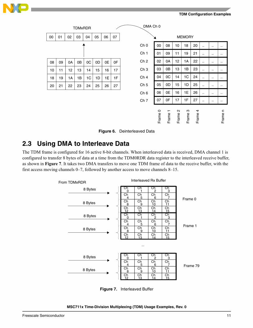
When data is deinterleaved, the data in each channel data is arranged in sequential order. That is, each channel of data for all frames is arranged in contiguous memory as shown in Figure 6. Frame 0 channel 0 data is followed by frame 1 channel 0 data, and so on.
MSC711x Time-Division Multiplexing (TDM) Usage Examples, Rev. 0
10 Freescale Semiconductor
TDM Configuration Examples
07 0F 17 1F 27 .. .. ..
06 0E 16 1E 26 .. .. ..
00 01 02 03 04 05 06 07
TDMxRDR
08 09 0A 0B 0C 0D 0E 0F
10 11 12 13 14 15 16 17
18 19 1A 1B 1C 1D 1E 1F
20 21 22 23 24 25 26 27
01 09 11 19 21 .. .. ..
02 0A 12 1A 22 .. .. ..
03 0B 13 1B 23 .. .. ..
04 0C 14 1C 24 .. .. ..
00 08 10 18 20 .. .. ..
DMA Ch 0
MEMORY
Fram
e 0
Ch 0
Ch 1
Ch 2
Ch 3
Ch 4
Ch 5
Ch 6
Ch 7
05 0D 15 1D 25 .. .. ..
Fram
e 1
Fram
e 2
Fram
e n
Fram
e 3
Fram
e 4
Figure 6. Deinterleaved Data
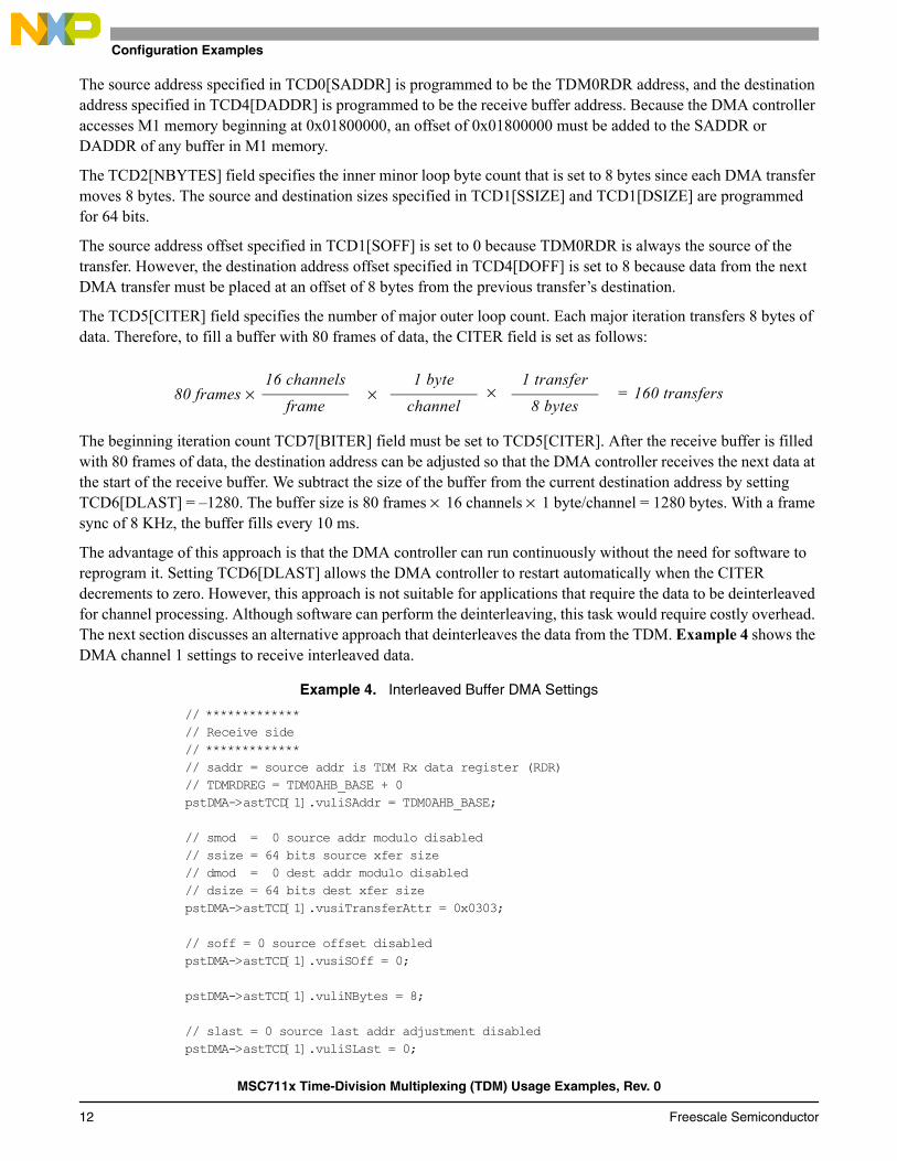
2.3 Using DMA to Interleave DataThe TDM frame is configured for 16 active 8-bit channels. When interleaved data is received, DMA channel 1 is configured to transfer 8 bytes of data at a time from the TDM0RDR data register to the interleaved receive buffer, as shown in Figure 7. It takes two DMA transfers to move one TDM frame of data to the receive buffer, with the first access moving channels 0–7, followed by another access to move channels 8–15.
Interleaved Rx BufferFrom TDMxRDR
Ch0
Ch1
Ch2
Ch38 Bytes
Ch4
Ch5
Ch6
Ch7
Ch8
Ch9
Ch10
Ch11
Ch12
Ch13
Ch14
Ch15
Frame 0
Ch0
Ch1
Ch2
Ch3
Ch4
Ch5
Ch6
Ch7
Ch8
Ch9
Ch10
Ch11
Ch12
Ch13
Ch14
Ch15
Frame 1
Ch0
Ch1
Ch2
Ch3
Ch4
Ch5
Ch6
Ch7
Ch8
Ch9
Ch10
Ch11
Ch12
Ch13
Ch14
Ch15
Frame 79
8 Bytes
8 Bytes
8 Bytes
8 Bytes
8 Bytes
...
Figure 7. Interleaved Buffer
MSC711x Time-Division Multiplexing (TDM) Usage Examples, Rev. 0
Freescale Semiconductor 11
TDM Configuration Examples
The source address specified in TCD0[SADDR] is programmed to be the TDM0RDR address, and the destination address specified in TCD4[DADDR] is programmed to be the receive buffer address. Because the DMA controller accesses M1 memory beginning at 0x01800000, an offset of 0x01800000 must be added to the SADDR or DADDR of any buffer in M1 memory.
The TCD2[NBYTES] field specifies the inner minor loop byte count that is set to 8 bytes since each DMA transfer moves 8 bytes. The source and destination sizes specified in TCD1[SSIZE] and TCD1[DSIZE] are programmed for 64 bits.
The source address offset specified in TCD1[SOFF] is set to 0 because TDM0RDR is always the source of the transfer. However, the destination address offset specified in TCD4[DOFF] is set to 8 because data from the next DMA transfer must be placed at an offset of 8 bytes from the previous transfer’s destination.
The TCD5[CITER] field specifies the number of major outer loop count. Each major iteration transfers 8 bytes of data. Therefore, to fill a buffer with 80 frames of data, the CITER field is set as follows:
80 frames × 16 channels
frame
1 byte
channel
1 transfer
8 bytes× × = 160 transfers
The beginning iteration count TCD7[BITER] field must be set to TCD5[CITER]. After the receive buffer is filled with 80 frames of data, the destination address can be adjusted so that the DMA controller receives the next data at the start of the receive buffer. We subtract the size of the buffer from the current destination address by setting TCD6[DLAST] = –1280. The buffer size is 80 frames × 16 channels × 1 byte/channel = 1280 bytes. With a frame sync of 8 KHz, the buffer fills every 10 ms.
The advantage of this approach is that the DMA controller can run continuously without the need for software to reprogram it. Setting TCD6[DLAST] allows the DMA controller to restart automatically when the CITER decrements to zero. However, this approach is not suitable for applications that require the data to be deinterleaved for channel processing. Although software can perform the deinterleaving, this task would require costly overhead. The next section discusses an alternative approach that deinterleaves the data from the TDM. Example 4 shows the DMA channel 1 settings to receive interleaved data.
Example 4. Interleaved Buffer DMA Settings
// *************// Receive side// *************// saddr = source addr is TDM Rx data register (RDR)// TDMRDREG = TDM0AHB_BASE + 0pstDMA->astTCD[1].vuliSAddr = TDM0AHB_BASE;
// smod = 0 source addr modulo disabled// ssize = 64 bits source xfer size // dmod = 0 dest addr modulo disabled// dsize = 64 bits dest xfer sizepstDMA->astTCD[1].vusiTransferAttr = 0x0303;
// soff = 0 source offset disabledpstDMA->astTCD[1].vusiSOff = 0;
pstDMA->astTCD[1].vuliNBytes = 8;
// slast = 0 source last addr adjustment disabledpstDMA->astTCD[1].vuliSLast = 0;
MSC711x Time-Division Multiplexing (TDM) Usage Examples, Rev. 0
12 Freescale Semiconductor
TDM Configuration Examples
addr = (UWord32)(&Rx_buffer);// daddr = dest addr is Rx_buffer;pstDMA->astTCD[1].vuliDAddr = COMP_DMA_ADDR(addr);
// SZ_BUF = 80 * 16 * 1 = 1280pstDMA->astTCD[1].vusiCIter = SZ_BUF / 8;
// First 8 bytes received are 0 (data already in FIFO) so// receive additional 8 bytespstDMA->astTCD[1].vusiDOff = 8;
// Adjust destination addresspstDMA->astTCD[1].vuliDLastSGA = -(SZ_BUF);
// Biter = CiterpstDMA->astTCD[1].vusiBIter = pstDMA->astTCD[1].vusiCIter;
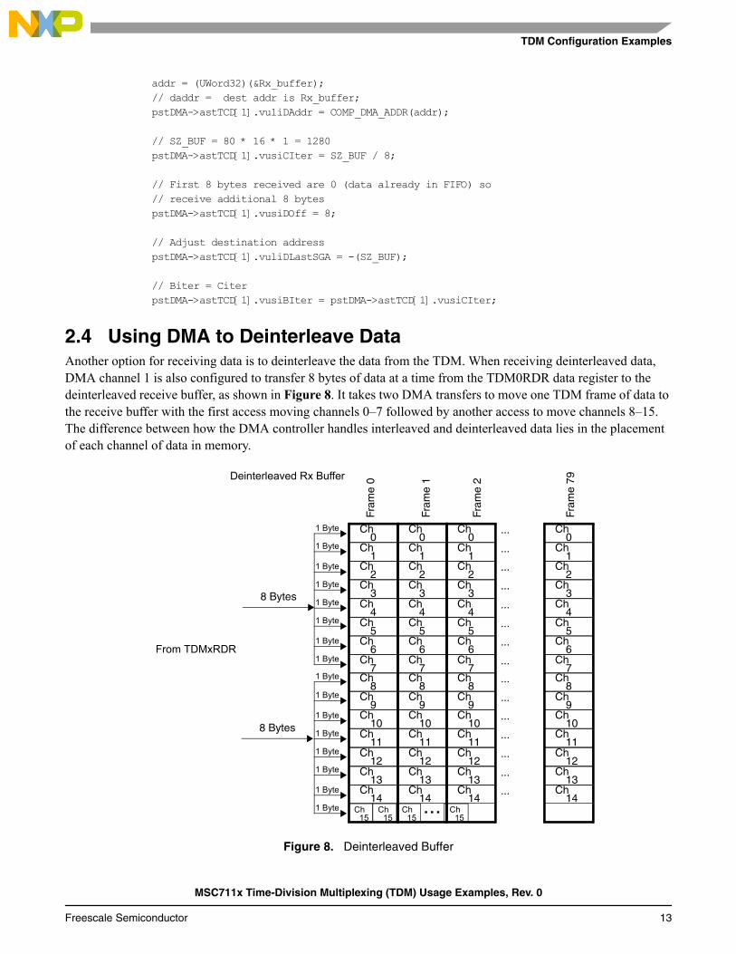
2.4 Using DMA to Deinterleave DataAnother option for receiving data is to deinterleave the data from the TDM. When receiving deinterleaved data, DMA channel 1 is also configured to transfer 8 bytes of data at a time from the TDM0RDR data register to the deinterleaved receive buffer, as shown in Figure 8. It takes two DMA transfers to move one TDM frame of data to the receive buffer with the first access moving channels 0–7 followed by another access to move channels 8–15. The difference between how the DMA controller handles interleaved and deinterleaved data lies in the placement of each channel of data in memory.
Deinterleaved Rx Buffer
From TDMxRDR
Ch0
Ch0
Ch0
8 Bytes
Fram
e 0
... Ch0
Fram
e 1
Fram
e 2
Fram
e 79
Ch1
Ch1
Ch1
... Ch1
Ch2
Ch2
Ch2
... Ch2
Ch3
Ch3
Ch3
... Ch3
Ch4
Ch4
Ch4
... Ch4
Ch5
Ch5
Ch5
... Ch5
Ch6
Ch6
Ch6
... Ch6
Ch7
Ch7
Ch7
... Ch7
Ch8
Ch8
Ch8
... Ch8
Ch9
Ch9
Ch9
... Ch9
Ch10
Ch10
Ch10
... Ch10
Ch11
Ch11
Ch11
... Ch11
Ch12
Ch12
Ch12
... Ch12
Ch13
Ch13
Ch13
... Ch13
Ch14
Ch14
Ch14
... Ch14
Ch15
Ch15
Ch15
... Ch15
1 Byte
1 Byte
1 Byte
1 Byte
1 Byte
1 Byte
1 Byte
1 Byte
1 Byte
1 Byte
1 Byte
1 Byte
1 Byte
1 Byte
1 Byte
1 Byte
8 Bytes
Figure 8. Deinterleaved Buffer
MSC711x Time-Division Multiplexing (TDM) Usage Examples, Rev. 0
Freescale Semiconductor 13
TDM Configuration Examples
TCD0[SADDR] and TCD4[DADDR] are configured the same way as in Section 2.4, Using DMA to Deinterleave Data, on page 13, with the TDM0RDR as the source and the receive buffer as the destination.
TCD2[NBYTES], TCD1[SSIZE], and TCD1[SOFF] also remain configured the same way, and each DMA transfer moves 8 bytes at a time from the TDM0RDR. However, since data is deinterleaved, channel data is arranged in contiguous memory. When the DMA takes 8 bytes from TDM0RDR, it must place each channel of data into its own channel buffer. In each DMA request, the DMA controller performs one read from the TDM0RDR of 8 bytes and then it performs eight writes of one byte each to the receive buffer so that TCD1[DSIZE] is set to one byte. Each channel of data is stored at an offset equal to the size of the channel buffer. In this example, each channel buffer holds 80 frames of data or 80 bytes. Therefore, TCD4[DOFF] is set to 80. It takes two DMA requests to transfer one frame of data, so the TCD5[CITER] field is set to 2. The first transfer moves channels 0–7, and the second transfer moves channels 8–15. TCD7[BITER] is also set to 2.
1 frame × 16 channels
frame
1 byte
channel
1 transfer
8 bytes× × = 2 transfers
After the first frame is received, the next destination address is adjusted so that next frame starts in the memory location that holds channel 0 of the next frame. That is, TCD6[DLAST] = –(1280 – 1). Example 5 shows the DMA channel 1 settings to receive deinterleaved data.
Example 5. Deinterleave Buffer DMA Settings
// *************// Receive side// *************// saddr = source addr is TDM Rx data register// TDMRDREG = TDM0AHB_BASE + 0pstDMA->astTCD[1].vuliSAddr = TDM0AHB_BASE;
// smod = 0 source addr modulo disabled// ssize= 64 bits source xfer size // dmod = 0 dest addr modulo disabled// dize = 8 bitspstDMA->astTCD[1].vusiTransferAttr = 0x0300;
// soff = 0 source offset disabledpstDMA->astTCD[1].vusiSOff = 0;
pstDMA->astTCD[1].vuliNBytes = 8;
// slast = 0 source last addr adjustment disabledpstDMA->astTCD[1].vuliSLast = 0;
addr = (UWord32)(&Rx_buffer);// daddr = dest addr is Rx_buffer;pstDMA->astTCD[1].vuliDAddr = COMP_DMA_ADDR(addr);
pstDMA->astTCD[1].vusiCIter = NUM_CH*SZ_CH/8;
//SZ_CH * NUM_FRM = 80pstDMA->astTCD[1].vusiDOff = SZ_CH*NUM_FRM;
pstDMA->astTCD[1].vuliDLastSGA = -(SZ_BUF-SZ_CH);
MSC711x Time-Division Multiplexing (TDM) Usage Examples, Rev. 0
14 Freescale Semiconductor
TDM Configuration Examples
pstDMA->astTCD[1].vusiBIter = pstDMA->astTCD[1].vusiCIter;
// bwc = 0// major.linkch = 0// major.e_link = 0// e_sg = 0// d_req = 0// int_half = 0// int_maj = 1// start = 0pstDMA->astTCD[1].vusiChannelCtrlStat = 0x02;
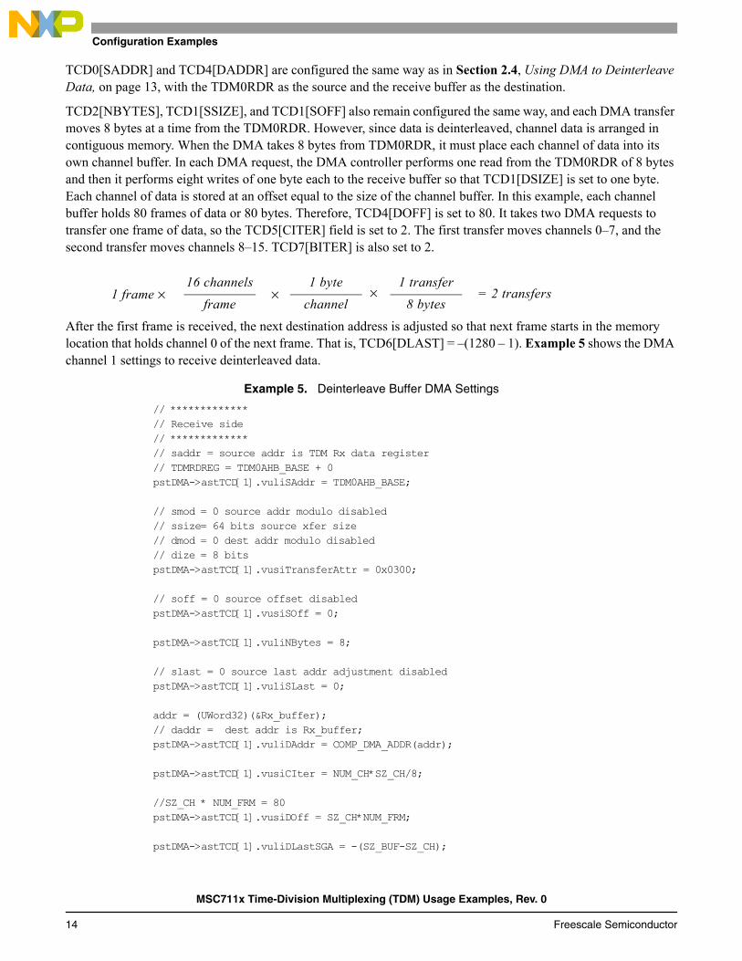
2.5 Interrupting Every n FramesThe example discussed in this section expands on the previous example. To configure the DMA to interrupt every n frames, another channel can be linked from the receive DMA channel 1. When this channel’s CITER = n, an interrupt is generated after n frames are received. Figure 9 shows a diagram of the channel linking when n = 4.
Deinterleaved Rx Buffer
From TDMxRDR
8 Bytes
Fram
e 0
Fram
e 1
Fram
e 2
Fram
e 79
...1 Byte
1 Byte
1 Byte
1 Byte
1 Byte
1 Byte
1 Byte
1 Byte
1 Byte
1 Byte
1 Byte
1 Byte
1 Byte
1 Byte
1 Byte
1 Byte
8 Bytes
Ch0
Ch1
Ch2
Ch3
Ch4
Ch5
Ch6
Ch7
Ch8
Ch9
Ch10
Ch11
Ch12
Ch13
Ch14
Ch15
Ch0
Ch1
Ch2
Ch3
Ch4
Ch5
Ch6
Ch7
Ch8
Ch9
Ch10
Ch11
Ch12
Ch13
Ch14
Ch15
Ch0
Ch1
Ch2
Ch3
Ch4
Ch5
Ch6
Ch7
Ch8
Ch9
Ch10
Ch11
Ch12
Ch13
Ch14
Ch15
Ch0
Ch1
Ch2
Ch3
Ch4
Ch5
Ch6
Ch7
Ch8
Ch9
Ch10
Ch11
Ch12
Ch13
Ch14
Ch15
...
...
...
...
...
...
...
...
...
...
...
Fram
e 3
Ch0
Ch1
Ch2
Ch3
Ch4
Ch5
Ch6
Ch7
Ch8
Ch9
Ch10
Ch11
Ch12
Ch13
Ch14
Ch15
DMA Channel 6CITER = 3
DMA Channel 6CITER = 2
DMA Channel 6CITER = 1
DMA Channel 6CITER = 0
DMAChannel 6Interrupt
Enable DMA channel 1 to DMA channel 6 linking.DMA channel 6 is active after one frame is received.DMA channel 6 genereates an interrupt after 4 frames are received.
Figure 9. Interrupt Every Four Frames
MSC711x Time-Division Multiplexing (TDM) Usage Examples, Rev. 0
Freescale Semiconductor 15
TDM Configuration Examples
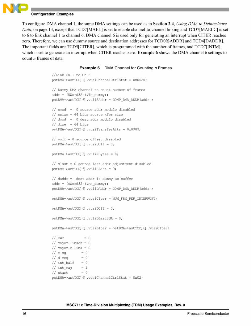
To configure DMA channel 1, the same DMA settings can be used as in Section 2.4, Using DMA to Deinterleave Data, on page 13, except that TCD7[MAEL] is set to enable channel-to-channel linking and TCD7[MAELC] is set to 6 to link channel 1 to channel 6. DMA channel 6 is used only for generating an interrupt when CITER reaches zero. Therefore, we can use dummy source and destination addresses for TCD0[SADDR] and TCD4[DADDR]. The important fields are TCD5[CITER], which is programmed with the number of frames, and TCD7[INTM], which is set to generate an interrupt when CITER reaches zero. Example 6 shows the DMA channel 6 settings to count n frames of data.
Example 6. DMA Channel for Counting n Frames
//Link Ch 1 to Ch 6pstDMA->astTCD[1].vusiChannelCtrlStat = 0x0620;
// Dummy DMA channel to count number of framesaddr = (UWord32)(&Tx_dummy);pstDMA->astTCD[6].vuliSAddr = COMP_DMA_ADDR(addr);
// smod = 0 source addr modulo disabled// ssize = 64 bits source xfer size // dmod = 0 dest addr modulo disabled
// dize = 64 bitspstDMA->astTCD[6].vusiTransferAttr = 0x0303;
// soff = 0 source offset disabledpstDMA->astTCD[6].vusiSOff = 0;
pstDMA->astTCD[6].vuliNBytes = 8;
// slast = 0 source last addr adjustment disabledpstDMA->astTCD[6].vuliSLast = 0;
// daddr = dest addr is dummy Rx bufferaddr = (UWord32)(&Rx_dummy);pstDMA->astTCD[6].vuliDAddr = COMP_DMA_ADDR(addr);
pstDMA->astTCD[6].vusiCIter = NUM_FRM_PER_INTERRUPT;
pstDMA->astTCD[6].vusiDOff = 0;
pstDMA->astTCD[6].vuliDLastSGA = 0;
pstDMA->astTCD[6].vusiBIter = pstDMA->astTCD[6].vusiCIter;
// bwc = 0// major.linkch = 0// major.e_link = 0// e_sg = 0// d_req = 0// int_half = 0// int_maj = 1// start = 0pstDMA->astTCD[6].vusiChannelCtrlStat = 0x02;
MSC711x Time-Division Multiplexing (TDM) Usage Examples, Rev. 0
16 Freescale Semiconductor
TDM Configuration Examples
The disadvantage of Example 2 and Example 3 is that after the buffer is filled with 80 frames of data, software must reprogram the DMA controller to start over. Unlike the previous example in which the DMA channel automatically starts receiving at the start of the buffer when CITER decrements to zero, the deinterleaved buffer structure prevents the DMA controller from returning to the start of the buffer after the buffer is filled. Restarting requires software to reprogram the DMA controller to receive data at the start of the buffer. DMA channel 6 could be used to interrupt after 80 frames so that the DMA controller can be reprogrammed. Although this approach allows the DMA to directly deinterleave data from the TDM, it also makes timing a critical issue because software must finish reprogramming the DMA controller before new data arrives. Otherwise, data is missed. The next example shows an alternative method.
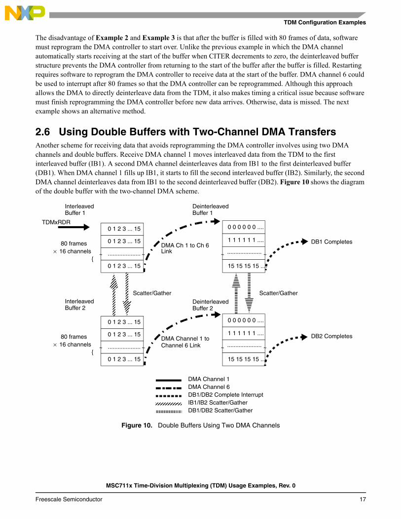
2.6 Using Double Buffers with Two-Channel DMA TransfersAnother scheme for receiving data that avoids reprogramming the DMA controller involves using two DMA channels and double buffers. Receive DMA channel 1 moves interleaved data from the TDM to the first interleaved buffer (IB1). A second DMA channel deinterleaves data from IB1 to the first deinterleaved buffer (DB1). When DMA channel 1 fills up IB1, it starts to fill the second interleaved buffer (IB2). Similarly, the second DMA channel deinterleaves data from IB1 to the second deinterleaved buffer (DB2). Figure 10 shows the diagram of the double buffer with the two-channel DMA scheme.
Interleaved
{
Interleaved
Buffer 1
Buffer 2
0 0 0 0 0 0 ....
1 1 1 1 1 1 ....
× 16 channels80 frames
.....................
15 15 15 15 ....
~ ~
0 0 0 0 0 0 ....
1 1 1 1 1 1 ....
.....................
15 15 15 15 ....
~ ~
Scatter/Gather
DMA Channel 1DMA Channel 6
DMA Channel 1 to
DMA Ch 1 to Ch 6Link
Scatter/Gather
0 1 2 3 ... 15
0 1 2 3 ... 15
....................
0 1 2 3 ... 15
~ ~
{× 16 channels
80 frames
0 1 2 3 ... 15
0 1 2 3 ... 15
....................
0 1 2 3 ... 15
~ ~
TDMxRDR
DeinterleavedBuffer 1
DeinterleavedBuffer 2
DB1/DB2 Complete Interrupt
DB1 Completes
DB2 Completes
IB1/IB2 Scatter/GatherDB1/DB2 Scatter/Gather
Channel 6 Link
Figure 10. Double Buffers Using Two DMA Channels
MSC711x Time-Division Multiplexing (TDM) Usage Examples, Rev. 0
Freescale Semiconductor 17
TDM Configuration Examples
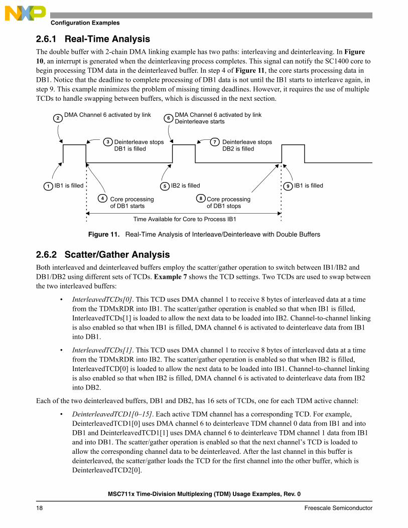
2.6.1 Real-Time AnalysisThe double buffer with 2-chain DMA linking example has two paths: interleaving and deinterleaving. In Figure 10, an interrupt is generated when the deinterleaving process completes. This signal can notify the SC1400 core to begin processing TDM data in the deinterleaved buffer. In step 4 of Figure 11, the core starts processing data in DB1. Notice that the deadline to complete processing of DB1 data is not until the IB1 starts to interleave again, in step 9. This example minimizes the problem of missing timing deadlines. However, it requires the use of multiple TCDs to handle swapping between buffers, which is discussed in the next section.
1 IB1 is filled
DMA Channel 6 activated by link2
3 Deinterleave stops
4 Core processing
5 IB2 is filled
DMA Channel 6 activated by link6
7
Deinterleave starts
Deinterleave stops
9 IB1 is filled
8 Core processing
Time Available for Core to Process IB1
DB1 is filled DB2 is filled
of DB1 starts of DB1 stops
Figure 11. Real-Time Analysis of Interleave/Deinterleave with Double Buffers
2.6.2 Scatter/Gather AnalysisBoth interleaved and deinterleaved buffers employ the scatter/gather operation to switch between IB1/IB2 and DB1/DB2 using different sets of TCDs. Example 7 shows the TCD settings. Two TCDs are used to swap between the two interleaved buffers:
• InterleavedTCDs[0]. This TCD uses DMA channel 1 to receive 8 bytes of interleaved data at a time from the TDMxRDR into IB1. The scatter/gather operation is enabled so that when IB1 is filled, InterleavedTCDs[1] is loaded to allow the next data to be loaded into IB2. Channel-to-channel linking is also enabled so that when IB1 is filled, DMA channel 6 is activated to deinterleave data from IB1 into DB1.
• InterleavedTCDs[1]. This TCD uses DMA channel 1 to receive 8 bytes of interleaved data at a time from the TDMxRDR into IB2. The scatter/gather operation is enabled so that when IB2 is filled, InterleavedTCD[0] is loaded to allow the next data to be loaded into IB1. Channel-to-channel linking is also enabled so that when IB2 is filled, DMA channel 6 is activated to deinterleave data from IB2 into DB2.
Each of the two deinterleaved buffers, DB1 and DB2, has 16 sets of TCDs, one for each TDM active channel:
• DeinterleavedTCD1[0–15]. Each active TDM channel has a corresponding TCD. For example, DeinterleavedTCD1[0] uses DMA channel 6 to deinterleave TDM channel 0 data from IB1 and into DB1 and DeinterleavedTCD1[1] uses DMA channel 6 to deinterleave TDM channel 1 data from IB1 and into DB1. The scatter/gather operation is enabled so that the next channel’s TCD is loaded to allow the corresponding channel data to be deinterleaved. After the last channel in this buffer is deinterleaved, the scatter/gather loads the TCD for the first channel into the other buffer, which is DeinterleavedTCD2[0].
MSC711x Time-Division Multiplexing (TDM) Usage Examples, Rev. 0
18 Freescale Semiconductor
TDM Configuration Examples
• DeinterleavedTCD2[0–15]. Each active TDM channel has a corresponding TCD. For example, DeinterleavedTCD2[0] uses DMA channel 6 to deinterleave TDM channel 0 data from IB2 and into DB2. DeinterleavedTCD2[1] uses DMA channel 6 to deinterleave TDM channel 1 data from IB2 and into DB2. The scatter/gather operation is enabled so that the next channel’s TCD is loaded to allow the corresponding channel data to be deinterleaved. After the last channel in this buffer is deinterleaved, the scatter/gather loads the TCD for the first channel into the other buffer, which is DeinterleavedTCD1[0].
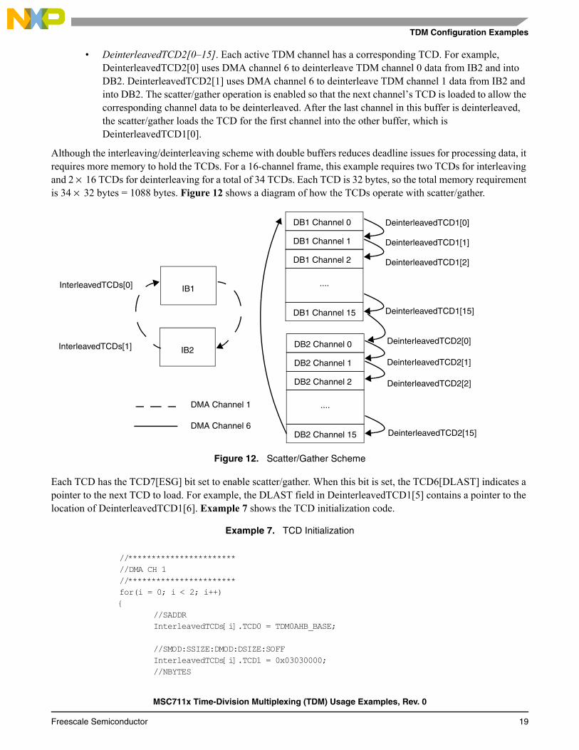
Although the interleaving/deinterleaving scheme with double buffers reduces deadline issues for processing data, it requires more memory to hold the TCDs. For a 16-channel frame, this example requires two TCDs for interleaving and 2 × 16 TCDs for deinterleaving for a total of 34 TCDs. Each TCD is 32 bytes, so the total memory requirement is 34 × 32 bytes = 1088 bytes. Figure 12 shows a diagram of how the TCDs operate with scatter/gather.
IB2InterleavedTCDs[1]
IB1InterleavedTCDs[0]
DB1 Channel 0
DB1 Channel 1
....
DB1 Channel 2
DB1 Channel 15
DeinterleavedTCD1[0]
DeinterleavedTCD1[1]
DeinterleavedTCD1[2]
DeinterleavedTCD1[15]
DB2 Channel 0
DB2 Channel 1
....
DB2 Channel 2
DB2 Channel 15
DeinterleavedTCD2[0]
DeinterleavedTCD2[1]
DeinterleavedTCD2[2]
DeinterleavedTCD2[15]
DMA Channel 1
DMA Channel 6
Figure 12. Scatter/Gather Scheme
Each TCD has the TCD7[ESG] bit set to enable scatter/gather. When this bit is set, the TCD6[DLAST] indicates a pointer to the next TCD to load. For example, the DLAST field in DeinterleavedTCD1[5] contains a pointer to the location of DeinterleavedTCD1[6]. Example 7 shows the TCD initialization code.
Example 7. TCD Initialization
//***********************//DMA CH 1//***********************for(i = 0; i < 2; i++){
//SADDRInterleavedTCDs[i].TCD0 = TDM0AHB_BASE;
//SMOD:SSIZE:DMOD:DSIZE:SOFFInterleavedTCDs[i].TCD1 = 0x03030000;//NBYTES
MSC711x Time-Division Multiplexing (TDM) Usage Examples, Rev. 0
Freescale Semiconductor 19
TDM Configuration Examples
InterleavedTCDs[i].TCD2 = 0x00000008;
//SLASTInterleavedTCDs[i].TCD3 = 0x00000000;
if(i == 0){
//DADDR addr = (UWord32)(&IB1);
InterleavedTCDs[i].TCD4 = COMP_DMA_ADDR(addr);
//DLASTaddr = (UWord32)(&InterleavedTCDs[1]);InterleavedTCDs[i].TCD6 = COMP_DMA_ADDR(addr);
}
else{
//DADDR addr = (UWord32)(&IB2);
InterleavedTCDs[i].TCD4 = COMP_DMA_ADDR(addr);
//DLASTaddr = (UWord32)(&InterleavedTCDs[0]);InterleavedTCDs[i].TCD6 = COMP_DMA_ADDR(addr);
}
//CITERE:CITERL:CITER:DOFFInterleavedTCDs[i].TCD5 = (SZ_BUF /8) << 16 | 0x00000008;
// ESG=1, INTM=1, MAELC=6, MAEL=1 InterleavedTCDs[i].TCD7 = (SZ_BUF /8) << 16 | 0x00000632;
//***********************//DMA CH 6//***********************for(i = 0; i < NUM_CH; i++){
//SADDR addr = (UWord32)(&IB1) + i * SZ_CH;
DeinterleavedTCD1[i].TCD0 = COMP_DMA_ADDR(addr);
addr = (UWord32)(&IB2) + i * SZ_CH;DeinterleavedTCD2[i].TCD0 = COMP_DMA_ADDR(addr);
//SMOD:SSIZE:DMOD:DSIZE:SOFFDeinterleavedTCD1[i].TCD1 = NUM_CH * SZ_CH;DeinterleavedTCD2[i].TCD1 = NUM_CH * SZ_CH;
//NBYTESDeinterleavedTCD1[i].TCD2 = NUM_FRM * SZ_CH;DeinterleavedTCD2[i].TCD2 = NUM_FRM * SZ_CH;
//SLASTDeinterleavedTCD1[i].TCD3 = 0x00000000;DeinterleavedTCD2[i].TCD3 = 0x00000000;
MSC711x Time-Division Multiplexing (TDM) Usage Examples, Rev. 0
20 Freescale Semiconductor
TDM Initialization
//DADDR addr = (UWord32)(&DB1) + i * NUM_FRM;
DeinterleavedTCD1[i].TCD4 = COMP_DMA_ADDR(addr);
addr = (UWord32)(&DB2) + i * NUM_FRM;DeinterleavedTCD2[i].TCD4 = COMP_DMA_ADDR(addr);
//CITERE:CITERL:CITER:DOFFDeinterleavedTCD1[i].TCD5 = 1 << 16 | 1;DeinterleavedTCD2[i].TCD5 = 1 << 16 | 1;
//Last TCD links to first TCD and interruptif(i == (NUM_CH - 1)){
//DLASTaddr = (UWord32)(&DeinterleavedTCD2[0]);DeinterleavedTCD1[i].TCD6 = COMP_DMA_ADDR(addr);
addr = (UWord32)(&DeinterleavedTCD1[0]);DeinterleavedTCD2[i].TCD6 = COMP_DMA_ADDR(addr);
// ESG=1, INTM=1DeinterleavedTCD1[i].TCD7 = 1 << 16 | 0x00000012;DeinterleavedTCD2[i].TCD7 = 1 << 16 | 0x00000012;
}
else{
//DLASTaddr = (UWord32)(&DeinterleavedTCD1[i+1]);DeinterleavedTCD1[i].TCD6 = COMP_DMA_ADDR(addr);
addr = (UWord32)(&DeinterleavedTCD2[i+1]);DeinterleavedTCD2[i].TCD6 = COMP_DMA_ADDR(addr);
// ESG=1 DeinterleavedTCD1[i].TCD7 = 1 << 16 | 0x00000010;DeinterleavedTCD2[i].TCD7 = 1 << 16 | 0x00000010;
}}
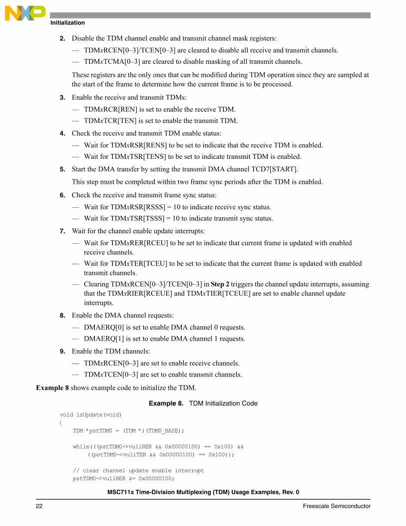
3 TDM Initialization To ensure proper operation of the TDM, registers must be initialized in the correct order. After the MSC711x is brought out of reset, software must initialize the TDM as follows:
1. Program the TDM configuration registers:— TDMxRIR/TIR define the receiver and transmitter interface operation.— TDMxRFP/TFP define the receiver and transmitter frame parameters.— TDMxGIR define the general interface operation.
These registers should not be modified when the TDM is enabled.
MSC711x Time-Division Multiplexing (TDM) Usage Examples, Rev. 0
Freescale Semiconductor 21
TDM Initialization
2. Disable the TDM channel enable and transmit channel mask registers:— TDMxRCEN[0–3]/TCEN[0–3] are cleared to disable all receive and transmit channels.— TDMxTCMA[0–3] are cleared to disable masking of all transmit channels.
These registers are the only ones that can be modified during TDM operation since they are sampled at the start of the frame to determine how the current frame is to be processed.
3. Enable the receive and transmit TDMs:— TDMxRCR[REN] is set to enable the receive TDM.— TDMxTCR[TEN] is set to enable the transmit TDM.
4. Check the receive and transmit TDM enable status:— Wait for TDMxRSR[RENS] to be set to indicate that the receive TDM is enabled.— Wait for TDMxTSR[TENS] to be set to indicate transmit TDM is enabled.
5. Start the DMA transfer by setting the transmit DMA channel TCD7[START].
This step must be completed within two frame sync periods after the TDM is enabled.
6. Check the receive and transmit frame sync status:— Wait for TDMxRSR[RSSS] = 10 to indicate receive sync status.— Wait for TDMxTSR[TSSS] = 10 to indicate transmit sync status.
7. Wait for the channel enable update interrupts:— Wait for TDMxRER[RCEU] to be set to indicate that current frame is updated with enabled
receive channels.— Wait for TDMxTER[TCEU] to be set to indicate that the current frame is updated with enabled
transmit channels.— Clearing TDMxRCEN[0–3]/TCEN[0–3] in Step 2 triggers the channel update interrupts, assuming
that the TDMxRIER[RCEUE] and TDMxTIER[TCEUE] are set to enable channel update interrupts.
8. Enable the DMA channel requests:— DMAERQ[0] is set to enable DMA channel 0 requests.— DMAERQ[1] is set to enable DMA channel 1 requests.
9. Enable the TDM channels:— TDMxRCEN[0–3] are set to enable receive channels.— TDMxTCEN[0–3] are set to enable transmit channels.
Example 8 shows example code to initialize the TDM.
Example 8. TDM Initialization Code
void isUpdate(void){ TDM *pstTDM0 = (TDM *)(TDM0_BASE);
while(((pstTDM0->vuliRER && 0x00000100) == 0x100) && ((pstTDM0->vuliTER && 0x00000100) == 0x100));
// clear channel update enable interrupt pstTDM0->vuliRER &= 0x00000100;
MSC711x Time-Division Multiplexing (TDM) Usage Examples, Rev. 0
22 Freescale Semiconductor
Dynamic Channel Configuration
pstTDM0->vuliTER &= 0x00000100;}
void StartTransfer(void){
// Deactivate all TDM channelspstTDM0->avuliRCEN[0] = 0L;pstTDM0->avuliTCEN[0] = 0L;
// Enable channel enable update interrupt pstTDM0->vuliRIER |= 0x00000100; pstTDM0->vuliTIER |= 0x00000100;
// Enable TDM RxpstTDM0->vuliRCR = 0x00000001;
// Enable TDM TxpstTDM0->vuliTCR = 0x00000001;
// Wait for TDM Rx/Tx enable statuswhile(pstTDM0->vuliTSR != 1);while(pstTDM0->vuliRSR != 1);
//Start Tx DMApstDMA->astTCD[0].vusiChannelCtrlStat = pstDMA->astTCD[0].vusiChannelCtrlStat | 0x0001;
// wait for syncwhile(((pstTDM0->vuliTSR>>1)&3) != 2);while(((pstTDM0->vuliRSR>>1)&3) != 2);
// wait for channel enable update interrupt isUpdate();
// Enable DMA chan 0 & 1 requestspstDMA->vuliDMAERQ = 0x00000003;
// Activate TDM channelspstTDM0->avuliRCEN[0] = 0x0000FFFF;pstTDM0->avuliTCEN[0] = 0x0000FFFF;
}
4 Dynamic Channel ConfigurationThe MSC711x TDM allows dynamic channel configuration so that channels can be activated or deactivated while the TDM is operating. During TDM operation, the receive and transmit channel enable registers TDMxRCEN[0–3]/TCEN[0–3] and transmit masking enable registers TDMxTCMA[0–3] can be changed at any time. These registers are sampled at the beginning of the frame to determine how the current frame is to be processed. The FIFO watermark should be set to 1 line so that the TDM does not process the next frame when activating or deactivating channels dynamically. When a buffer is filled, a DMA interrupt can be used to accommodate more or fewer channels.
MSC711x Time-Division Multiplexing (TDM) Usage Examples, Rev. 0
Freescale Semiconductor 23
System Tuning
The following steps outline the procedure to enable dynamic channel configuration:
1. Enable the channel enable update interrupts:— TDMxRIER[RCEUE] is set to enable the receive channel update interrupt.— TDMxTIER[TCEUE] is set to enable the transmit channel update interrupt.
2. Read TDMxRCEN0 then write back value to TDMxRCEN0:— Reading the channel enable register and writing back unmodified value generates a channel update
interrupt on a receive frame boundary.
3. Wait for the receive channel enable update interrupt:— Wait for TDMxRER[RCEU] to be set to indicate current frame is updated with enabled/disabled
receive channels.
4. Update new values to channel enable registers:— TDMxRCEN0:3 are updated to enable/disable receive channels.— TDMxTCEN0:3 are updated to enable/disable transmit channels.— TDMxTCMA0:3 are updated to enable masking of transmit channels.— Changes to the above registers must be completed within half of a frame period after receiving the
channel update interrupts in Step 3.
5. Wait for the next receive channel enable update interrupt:— Wait for TDMxRER[RCEU] to be set to indicate current frame is updated with enabled/disabled
receive channels.— Wait for TDMxTER[TCEU] to be set to indicate current frame is updated with enabled/disabled
transmit channels.— Read the TDMxRCEN[0–3], TDMxTCEN[0–3], and TDMxTCMA[0–3] to ensure that they
contain values written in Step 4.
6. If necessary, update any data structures for the TDM in memory.7. Disable the channel enable update interrupt
— TDMxRIER[RCEUE] is cleared to disable the receive channel update interrupt— TDMxTIER[TCEUE] is cleared to disable the transmit channel update interrupt
8. Return to normal processing.
5 System TuningThis section discusses how to tune the MSC711x modules with different arbitration schemes and priorities for best use of the system. For further details, see the System Usage and Tuning/Programming Reference in the MSC711x Reference Manual.
5.1 DMA PrioritiesThe 32 DMA channels are organized into two following groups:
• Group 0: Channels 0–15
• Group 1: Channels 16–31
MSC711x Time-Division Multiplexing (TDM) Usage Examples, Rev. 0
24 Freescale Semiconductor
System Tuning
DMA arbitration is based on group arbitration and channel arbitration schemes. Group arbitration is selected with the DMA Control Register DMACR[ERGA] bit. Group arbitration is handled as either fixed-priority or round robin-priority. When the ERGA bit is cleared, fixed-priority arbitration is used for selection between the groups. Setting DMACR[GRPxPRI] assigns the highest priority for the group. Each group must be programmed with a unique priority, and different groups cannot have the same priority level.
When the DMACR[ERGA] bit is set, round-robin group arbitration mode is selected, and groups are serviced from the highest group number to the lowest group number.
The channel arbitration scheme is selected via the DMACR[ERCA] bit. When this bit is cleared, fixed-priority arbitration is used among channels. One of 16 priority levels is assigned to each channel in the DMA Channel Priority Registers DCHPRIx. Each channel must be programmed with a unique priority, and different channels cannot have the same priority level. When all channels are programmed for fixed-priority arbitration, each channel can be individually programmed to enable or disable preemption by a higher-priority channel. If preemption is enabled, a request from a higher-priority channel preempts the current active channel and switches to the new one. If preemption is disabled, higher-priority channels gain control only upon completion of the current channel’s minor loop. Nested preemption is not permitted, so a DMA channel that has preempted another channel cannot be preempted. Preemption is available only in fixed-priority mode. It is not available in round-robin mode.
When the DMACR[ERCA] bit is set, round-robin channel arbitration is selected. Channel service starts at the highest channel number and rotates through to the lowest channel number without regard to channel priority levels.
It is important to ensure that long latencies do not occur before a high-priority channel is serviced. For example, while the first DMA channel is processed, it is preempted by a second higher-priority channel with a large byte count. If a third DMA request comes from a peripheral such as the TDM with a priority higher than the first and second channel, this channel must wait until the second channel completes before it can preempt because nested preemption is not allowed.
One way to minimize latency is to ensure that only one preemptable, lower-priority channel with a large bye count is active at a time. If the DMA channels not associated with a peripheral can run to completion without being preempted, there is no issue with latency because only the DMA channels associated with a peripheral can preempt another channel. This can be achieved by channel linking so that when one preemptable channel completes, it continues with the next channel in the chain.
5.2 Crossbar Switch TuningThe crossbar switch ensures that the SC1400 core can focus on the intensive computational work while the DMA controller brings in data for core processing. The crossbar switch slaves are configured as follows via the bits in the Slave General-Purpose Registers (SGPCR[0–5]):
• The port 0 crossbar switch slave M1 memory (ASM1) SGPCR0[HPEx] bit is set to enable the DMA master port. All other master ports are disabled.
• The port 1 crossbar switch slave M2 memory (ASM2) SGPCR1[HPEx] is set to enable the IFU, DMA and ECI master ports. All other master ports are disabled.
• The port 2 crossbar switch slave to external memory (ASEMI) SGPCR2[HPEx] bit set to enable the IFU, DMA controller, and ECI master ports.
• The port 3 crossbar switch slave to TDM/HDI16 (ASTH) SGPCR3[HPEx] bit is set to enable the DMA master port. All other master ports are disabled.
• The port 4 crossbar switch slave to the IPBus (ASSB) SGPCR4[HPEx] bit is set to enable the ECI master port. All other master ports are disabled.
MSC711x Time-Division Multiplexing (TDM) Usage Examples, Rev. 0
Freescale Semiconductor 25
System Tuning
• The port 5 crossbar switch slave to the APB (ASAPB) SGPCR5[HPEx] bit is set to enable the ECI master port. All other master ports are disabled.
In the ASM1 ASM2, ASEMI, and ASTH crossbar switch slaves, the Master Priority Register MPR[0–5] assigns the Ethernet master the highest priority followed by the DMA master. However, priority elevation can be used to elevate the TDM DMA priority. In the ASSB and ASAPB crossbar switch slaves, the ECI has the highest priority, followed by the DMA controller. Example 9 shows how to configure the crossbar switch.
Example 9. Crossbar Switch Configuration
/* // SGCPR fieldsHPE_IFU0x00040000 PARK_ON_FIXED 0x00000000HPE_DMA 0x00020000 PARK_ON_LAST 0x00000010HPE_ECI 0x00010000 PARK_ON_NONE 0x00000020
ARB_FIXED 0x00000000FIXED_IS_ECI 0x00000000ARB_ROUND 0x00000100FIXED_IS_DMA 0x00000001
FIXED_IS_IFU 0x00000002FIXED_IS_ENET 0x00000003
// MPR prioritiesENET_PRIO_0 0x00000000IFU_PRIO_0 0x00000000ENET_PRIO_1 0x00001000IFU_PRIO_1 0x00000100ENET_PRIO_2 0x00002000IFU_PRIO_2 0x00000200ENET_PRIO_3 0x00003000IFU_PRIO_3 0x00000300ENET_PRIO_4 0x00004000IFU_PRIO_4 0x00000400ENET_PRIO_5 0x00005000IFU_PRIO_5 0x00000500ENET_PRIO_6 0x00006000IFU_PRIO_6 0x00000600ENET_PRIO_7 0x00007000IFU_PRIO_7 0x00000700
DMA_PRIO_0 0x00000000ECI_PRIO_0 0x00000000DMA_PRIO_1 0x00000010ECI_PRIO_1 0x00000001DMA_PRIO_2 0x00000020ECI_PRIO_2 0x00000002DMA_PRIO_3 0x00000030ECI_PRIO_3 0x00000003DMA_PRIO_4 0x00000040ECI_PRIO_4 0x00000004DMA_PRIO_5 0x00000050ECI_PRIO_5 0x00000005DMA_PRIO_6 0x00000060ECI_PRIO_6 0x00000006DMA_PRIO_7 0x00000070ECI_PRIO_7 0x00000007
*/
/* port 0 - ASM1 slave to M1 */
HPE = HPE_DMA; ARB = ARB_FIXED; PCTL = PARK_ON_FIXED; PARK = FIXED_IS_DMA;
SGCPR0 = HPE | ARB | PCTL | PARK;
/* ENET highest - but use elevation to get TDM DMA higher still, IFU and * ECI should never access via this port anyway */ MPR0 = ENET_PRIO_0 | IFU_PRIO_6 | DMA_PRIO_1 | ECI_PRIO_7;
/* port 1 - ASM2 slave to M2 */
MSC711x Time-Division Multiplexing (TDM) Usage Examples, Rev. 0
26 Freescale Semiconductor
System Tuning
HPE = HPE_IFU | HPE_DMA | HPE_ECI; ARB = ARB_FIXED; PCTL = PARK_ON_FIXED; PARK = FIXED_IS_IFU;
SGCPR1 = HPE | ARB | PCTL | PARK; /* ENET highest, then DMA but use elevation for TDM, then IFU, then * ECI-- but parking on IFU as a compromise. Good to experiment with * these settings. */ MPR1 = ENET_PRIO_0 | IFU_PRIO_2 | DMA_PRIO_1 | ECI_PRIO_3;
/* port 2 - ASEMI slave to external memory */
HPE = HPE_IFU | HPE_DMA | HPE_ECI; ARB = ARB_FIXED; PCTL = PARK_ON_FIXED; PARK = FIXED_IS_DMA;
SGCPR2 = HPE | ARB | PCTL | PARK; /* ENET highest, then DMA but use elevation for TDM, then IFU, then * ECI. Good to experiment with these settings. */ MPR2 = ENET_PRIO_0 | IFU_PRIO_2 | DMA_PRIO_1 | ECI_PRIO_3;
/* port 3 - ASTH slave to TDM/HDI16 */
HPE = HPE_DMA; ARB = ARB_FIXED; PCTL = PARK_ON_FIXED; PARK = FIXED_IS_DMA;
SGCPR3 = HPE |ARB | PCTL | PARK; MPR3 = ENET_PRIO_0 | IFU_PRIO_6 | DMA_PRIO_1 | ECI_PRIO_3;
/* port 4 - ASSB slave to IPBus (I2C, etc) */
HPE = HPE_ECI; ARB = ARB_FIXED; PCTL = PARK_ON_FIXED; PARK = FIXED_IS_ECI;
SGCPR4 = HPE | ARB | PCTL | PARK; MPR4 = ENET_PRIO_6 | IFU_PRIO_7 | DMA_PRIO_1 | ECI_PRIO_0;
/* port 5 - ASAPB slave to APB (UART, etc) */
HPE = HPE_ECI; ARB = ARB_FIXED; PCTL = PARK_ON_FIXED; PARK = FIXED_IS_ECI;
SGCPR5 = HPE | ARB | PCTL | PARK; MPR5 = ENET_PRIO_6 | IFU_PRIO_7 | DMA_PRIO_1 | ECI_PRIO_0;
MSC711x Time-Division Multiplexing (TDM) Usage Examples, Rev. 0
Freescale Semiconductor 27
Document Order No.: AN2946
Information in this document is provided solely to enable system and software implementers to use Freescale Semiconductor products. There are no express or implied copyright licenses granted hereunder to design or fabricate any integrated circuits or integrated circuits based on the information in this document.
Freescale Semiconductor reserves the right to make changes without further notice to any products herein. Freescale Semiconductor makes no warranty, representation or guarantee regarding the suitability of its products for any particular purpose, nor does Freescale Semiconductor assume any liability arising out of the application or use of any product or circuit, and specifically disclaims any and all liability, including without limitation consequential or incidental damages. “Typical” parameters which may be provided in Freescale Semiconductor data sheets and/or specifications can and do vary in different applications and actual performance may vary over time. All operating parameters, including “Typicals” must be validated for each customer application by customer’s technical experts. Freescale Semiconductor does not convey any license under its patent rights nor the rights of others. Freescale Semiconductor products are not designed, intended, or authorized for use as components in systems intended for surgical implant into the body, or other applications intended to support or sustain life, or for any other application in which the failure of the Freescale Semiconductor product could create a situation where personal injury or death may occur. Should Buyer purchase or use Freescale Semiconductor products for any such unintended or unauthorized application, Buyer shall indemnify and hold Freescale Semiconductor and its officers, employees, subsidiaries, affiliates, and distributors harmless against all claims, costs, damages, and expenses, and reasonable attorney fees arising out of, directly or indirectly, any claim of personal injury or death associated with such unintended or unauthorized use, even if such claim alleges that Freescale Semiconductor was negligent regarding the design or manufacture of the part.
Freescale™ and the Freescale logo are trademarks of Freescale Semiconductor, Inc. StarCore is a trademark of StarCore LLC. All other product or service names are the property of their respective owners.
© Freescale Semiconductor, Inc. 2005.
How to Reach Us:Home Page:www.freescale.com
E-mail:[email protected]
USA/Europe or Locations not listed:Freescale Semiconductor Technical Information Center, CH3701300 N. Alma School RoadChandler, Arizona 85224+1-800-521-6274 or [email protected]
Europe, Middle East, and Africa:Freescale Halbleiter Deutschland GMBHTechnical Information CenterSchatzbogen 781829 München, Germany+44 1296 380 456 (English)+46 8 52200080 (English)+49 89 92103 559 (German)+33 1 69 35 48 48 (French)[email protected]
Japan:Freescale Semiconductor Japan Ltd. HeadquartersARCO Tower 15F1-8-1, Shimo-Meguro, Meguro-ku,Tokyo 153-0064, Japan0120 191014 or +81 3 5437 [email protected]
Asia/Pacific:Freescale Semiconductor Hong Kong Ltd.Technical Information Center2 Dai King StreetTai Po Industrial EstateTai Po, N.T. Hong Kong+800 2666 8080
For Literature Requests Only:Freescale Semiconductor Literature Distribution CenterP.O. Box 5405Denver, Colorado 802171-800-441-2447 or 303-675-2140Fax: [email protected]
Rev. 02/2005