Embed Size (px)
Citation preview
MSC316DC High-Integrated IP Camera SoC
Processor
Preliminary Product Brief Version 0.3

© 2017 MStar Semiconductor, Inc. All rights reserved. MStar Semiconductor makes no representations or warranties including, for example but not limited to, warranties of merchantability, fitness for a particular purpose, non-infringement of any intellectual property right or the accuracy or completeness of this document, and reserves the right to make changes without further notice to any products herein to improve reliability, function or design. No responsibility is assumed by MStar Semiconductor arising out of the application or use of any product or circuit described herein; neither does it convey any license under its patent rights, nor the rights of others. MStar is a trademark of MStar Semiconductor, Inc. Other trademarks or names herein are only for identification purposes only and owned by their respective owners.

MSC316DC High-Integrated IP Camera SoC Processor
Preliminary Product Brief Version 0.3
Security Level: Confidential B - i - 5/5/2017 Copyright © 2017 MStar Semiconductor, Inc. All rights reserved.
REVISION HISTORY Revision No. Description Date
0.1 ü Initial release 03/01/2017
0.2 ü Updated Electrical Specifications 03/29/2017
0.3 ü Updated Block Diagram ü Updated Electrical Specifications
05/05/2017
MSC316DC High-Integrated IP Camera SoC Processor
Preliminary Product Brief Version 0.3
Security Level: Confidential B - 1 - 5/5/2017 Copyright © 2017 MStar Semiconductor, Inc. All rights reserved.
FEATURES
n High Performance Processor Core ü ARM Cortex-A7 single Core 800MHz ü Neon and FPU ü Memory Management Unit for Linux support ü DMA Engine
n Image/Video Processor ü Supports 10/12-bit parallel interface for raw
data input ü Supports MIPI interface with 2 data lanes and
1 clock lane ü Supports 8/10-bit CCIR656 interface ü Supports 2M pixels video recording and image
snapshot ü Bad pixel compensation ü Noise Reduction (NR) ü Optical black correction ü Lens shading compensation ü Auto White Balance (AWB) / Auto Exposure
(AE) / Auto Focus (AF) ü CFA color interpolation ü Color correction ü Gamma correction ü Video stabilization ü Wide Dynamic Range (WDR) ü Rotation with 90 or 270 degree ü Lens distortion correction ü Fully programmable multi-function scaling
engines n MStar Advanced Color Engine (MStarACE) ü Luma gain/offset adjustment ü Supports 2D peaking ü Horizontal noise masking ü Direct Luma Correction (DLC) ü Black/White Level Extension (BLE/WLE) ü IHC/ICC/IBC for chroma adjustment ü Histogram statistics
n H.265/HEVC Encoder ü Supports H.265/HEVC baseline and main
profile encoding ü Supports MVs: 32x32, 16x16, 8x8 ü Supports up to quarter-pixel ü Supports one reference frame ü Supports Max. 2Mp/30fps encoding
n H.264 Encoder ü Supports H.264 baseline and main profile
encoding ü Supports MVs: 16x16, 16x8, 8x16, 8x8, 8x4,
4x8, 4x4 ü Supports up to quarter-pixel ü Supports two reference frames ü Supports rate control and ROI ü Supports Max. 2Mp/30fps encoding
n JPEG Encoder ü Supports JPEG baseline encoding ü Supports YUV422 or YUV420 formats
n Video Encoding Performance ü Supports 2Mp30 + +VGAp30+ QCIFp30
H.265/HEVC or H.264 encoding ü Supports MJPEG up to 2Mp15fps encoding
n Audio Processor ü One mono ADC for microphone inputs ü One mono DAC for lineouts ü Supports 8K/16K/32KHz sampling rate audio
recording ü Digital and analog gain adjustment
n NOR Flash Interface ü Compliant with standard, dual and quad SPI
Flash memory components

MSC316DC High-Integrated IP Camera SoC Processor
Preliminary Product Brief Version 0.3
Security Level: Confidential B - 2 - 5/5/2017 Copyright © 2017 MStar Semiconductor, Inc. All rights reserved.
n SDIO 2.0 Interface ü Compatible with SDIO spec. 2.0, data bus 1/4
bit mode ü Compatible with SD spec. 2.0, data bus 1/4 bit
mode n USB 2.0 Interface ü One USB 2.0 configurable host or device − Host mode supports EHCI specification − Device mode supports 6 endpoints
n DRAM Memory ü Embedded DDR3 DRAM memory − Memory size up to 1Gb
n Connectivity ü Built-in 10/100M Ethernet MAC and Ethernet
PHY ü One USB 2.0 OTG Controller could be used for
USB Wi-Fi Dongle or Module ü One SDIO 2.0 Host Controller could be used for
SDIO Wi-Fi module ü Supports Wakeup on LAN (WOL)
n Security Engines ü Supports AES/DES/TDES ü Supports secure booting
n Peripherals ü Dedicated GPIOs for system control ü Four PWM outputs shared with GPIOs ü Two generic UARTs and one fast UART with
flow control ü Three generic timers and one watchdog timer ü Two SPI masters ü One I2C Masters ü Built-in SAR ADC with 3 channels analog inputs
for different kinds of applications ü One IR input
n Operating Voltage Range ü Core: 0.9V ü I/O: 1.8 ~ 3.3V ü DRAM: 1.5V ü Power Consumption: TBD
n Package ü M2QFN, 9mmx9mm
MSC316DC High-Integrated IP Camera SoC Processor
Preliminary Product Brief Version 0.3
Security Level: Confidential B - 3 - 5/5/2017 Copyright © 2017 MStar Semiconductor, Inc. All rights reserved.
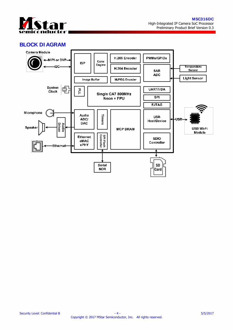
GENERAL DESCRIPTIONS The MSC316DC is a highly integrated SOC. Based on ARM Cortex-A7, it integrates Image Signal Processor (ISP), Color Engine, Video (H.264/H.265/MJPEG) Encoders and other useful peripherals for IP camera applications. A typical utilization of the MSC316DC application processor is demonstrated in the following block diagram. The complete system includes a camera module (CMOS sensor), a connectivity module (WiFi or Ethernet), and a non-volatile storage (NOR flash or SD card). The ISP and Color Engine handle images captured from the camera sensor, and the video stream is composed of lots images. There are pre- and post- video processing stages. The pre-video processing rotates images, reduces noises, enhances signals and translates color domains. The post-video processing corrects lens distortion, adjusts color quality, and generates multiple video streams with different resolutions. Multimedia Encoders can compress those video streams with different compressing standards at the same time. The well compressed video/audio streams could be streamed or stored in the cloud server through Wi-Fi or Ethernet or stored in a local SD Card. The NOR flash is usually reserved for operating system and application software. Moreover, other peripherals like SAR ADC, Audio ADC/DAC, UARTs, PWMs, GPIOs and SPI are supported to realize applications with maximal flexibility. Besides, the MSC316DC supports secure booting and personalization authentication mechanism for securing system. The AES/DES/3DES cipher engines could also help encrypt the compressed video/audio streams to protect privacy.
MSC316DC High-Integrated IP Camera SoC Processor
Preliminary Product Brief Version 0.3
Security Level: Confidential B - 4 - 5/5/2017 Copyright © 2017 MStar Semiconductor, Inc. All rights reserved.
BLOCK DIAGRAM
PLL
SPI FlashC
ontrollerTim
ersAudio
Driver
MSC316DC High-Integrated IP Camera SoC Processor
Preliminary Product Brief Version 0.3
Security Level: Confidential B - 5 - 5/5/2017 Copyright © 2017 MStar Semiconductor, Inc. All rights reserved.
FUNCTIONAL DESCRIPTION
Video Encoder I. JPE Feature Description n JPE features ü Supports JPEG encoding 3Mp − Frame mode − IMI row mode
ü Supports YUYV input format ü Supports NV12 input format ü Supports DCT mode to accelerate SW encoding
II. H.264 Feature Description n H.264 features ü Supports H264 baseline encoding ü Baseline profile, level 3.0 ü Supports MVs: 16x16, 16x8, 8x16, 8x8, 8x4, 4x8, 4x4 ü Supports up to quarter-pel ü Supports up to two reference frames ü Max resolutions − H264 supported are 2Mp
ü Frame-level & mb-level rate control ü Supports YUYV input format ü Supports NV12 input format ü Supports 16/235 and 0/255 Range Converter ü Supports cost-penalty adjustment ü Supports force zero-motion ü Supports intra16x16 planar mode
n Stream combination ü 2M@30fps+VGA@30fps+CIF@30fps ü 960p@30fps+VGA@30fps+CIF@30fps ü 960p@30fps+D1@30fps
MSC316DC High-Integrated IP Camera SoC Processor
Preliminary Product Brief Version 0.3
Security Level: Confidential B - 6 - 5/5/2017 Copyright © 2017 MStar Semiconductor, Inc. All rights reserved.
III. H.265 Brief Feature Description n Stream combination ü 2M@30fps+VGA@30fps+CIF@30fps ü 960p@30fps+VGA@30fps+CIF@30fps ü 960p@30fps+D1@30fps
ISP I. Brief Feature Description The ISP design is used to transfer raw sensor data output to YUV data and also supports YUV sensor at ISP bypass mode default.
ü Supports to FHD@30Hz, 2M@30, sensor input ü Fix pattern noise correction ü Bad pixel compensation ü Green equal ü Supports rgbir2x2 or rgbir4x4 mode input ü Optical black correction ü Len shading compensation ü Asymmetric Lens shading compensation ü Statistic for AWB/AE/AF ü Bayer domain de-noise ü Supports Bayer domain rotation ü White Balance PreGain and PostGain can be enable at the same time. ü CFA color interpolation ü Gamma correction ü Video stabilization statistic ü Supports menuload for ALSC_gain/DefectPxl/Gamma table
Peripheral I. USB Brief Feature Description One port of host/OTG controller is fully compliant with the USB 2.0 specification and the Enhanced Host Controller Interface (EHCI) specification. This Host/OTG Controller can support FS/LS transactions, Interrupt/Control/Bulk transfers and split/preamble transactions for hub. II. MIPI CSI Interface The features are listed below: ü CSI-2 1.1/D-PHY 1.1 compliant receiver with maximum Input Frequency 1GHz ü Supports 1 clock lane, 2 data lanes ü Supports YUV422 8-bit, Raw8, Raw10, Raw12, Generic 8-bit long packet and User defined byte-based data
type ü Supports 1-bit error correction/2-bit error detection for packet header ü Supports checksum error detection for payload data
MSC316DC High-Integrated IP Camera SoC Processor
Preliminary Product Brief Version 0.3
Security Level: Confidential B - 7 - 5/5/2017 Copyright © 2017 MStar Semiconductor, Inc. All rights reserved.
ü Supports timing generation for Vsync and Hsync III. Ethernet MAC Brief Feature Description ü IEEE Std 802.3 compatible ü Supports 10/100 Mbit/s operation. ü Full/Half duplex support. ü Automatic pad and CRC generation on transmitted packet. ü Supports transmit packet(IP/TCP/UDP) checksum generate ü Receiver & Transmitter Packet management by internal storage with descriptor header control ü Internal async-FIFO for receiver & transmitter frame wire speed operation ü Supports Tagged frame ü Supports IPV6 check-sum ü Supports IEEE802.3az EEE function
IV. EPHY Brief Feature Description The Ethernet PHY (EPHY) is an IEEE 802.3 compliant single-port Ethernet Transceiver for both 100Mbps and 10Mbps operations. The EPHY acts as an interface between the physical signaling and the Media Access Controller (MAC). It supports the Auto-Negotiation function to simplify the network installation and maintenance. The major functions of EPHY included: ü 10/100Mbps TX/RX ü Full-duplex or half duplex ü Supports IEEE 802.3u auto-negotiation ü DSP-based PHY Transceiver technology ü Supports WOL (Wake on Lan) feature (Magic Packet only) ü Supports IEEE 802.3az EEE function
V. Encryption Brief Feature Description AESDMA is a secure IP for Secure Boot and HDMI Key Authentication. There are three engines inside this IP: ü AES: ECB, CBC (dvs042), ECB_CTS, CBC_CTS, CTR ü SHA: SHA_1, SHA_256 ü RSA: RSA_2048 in HW key mode, programmable size in SW key mode
MSC316DC High-Integrated IP Camera SoC Processor
Preliminary Product Brief Version 0.3
Security Level: Confidential B - 8 - 5/5/2017 Copyright © 2017 MStar Semiconductor, Inc. All rights reserved.
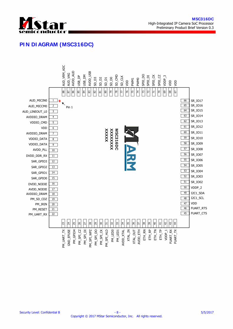
PIN DIAGRAM (MSC316DC)
8081828385 84 7677787986 75
6
7
8
9
11
12
10
2
1
3
4
5
Pin 1
13
14
74 73
15
16
17
18
19
20
59
58
57
56
54
53
55
63
64
62
61
60
52
51
50
49
48
47
46
45
707172 69 68 67
2928272624 25 3332313023 34 35 36 393837 40 41 42
DVDD_DDR_RX
SAR_GPIO3
SAR_GPIO2
SAR_GPIO1
SAR_GPIO0
VDDIO_DATA
AVDD_PLL
AVDD_NODIE
PM_SD_CDZ
AVDDIO_DRAM
DVDD_NODIE
PM_IRIN
AUD_MICIN0
AUD_MICCM0
AUD_LINEOUT_L0
AVDDIO_DRAM
VDDIO_CMD
VDD
AVDDIO_DRAM
VDDIO_DATA
ETH
_TN
PM_L
ED0
PM_S
PI_D
I
XTAL
_OU
T
PM_L
ED1
ETH
_RP
ETH
_RN
PM_S
PI_C
Z
AVD
D_E
TH
PM_S
PI_H
LD
VDD
P_1
PM_G
PIO
4
ETH
_TP
PM_S
PI_W
PZ
PM_S
PI_D
O
PM_S
PI_C
K
GN
D_E
FUSE
PM_U
ART_
TX
AVD
D_X
TAL
XTAL
_IN
SR_IO07
SR_IO08
SR_IO06
SR_IO13
SR_IO14
SR_IO15
SR_IO12
SR_IO09
FUART_CTS
FUART_RTS
I2C1_SCL
I2C1_SDA
VDD
SR_IO05
SR_IO04
VDDP_2
SR_IO02
SR_IO03
SR_IO10
SR_IO11
SPI0
_DO
PWM
1
PWM
0
SD_D
1
VDD
SPI0
_DI
SPI0
_CK
SD_D
3
AVD
D_U
SB
SD_D
2
USB
_DM
VDD
SD_C
LK
VDD
VDD
P_3
SPI0
_CZ
USB
_DP
AVD
D_A
UD
SD_C
MD
SD_D
0
21
22
PM_RESET
PM_UART_RX
43 44
FUAR
T_RX
FUAR
T_TX
65
66
8788
SR_IO16SR_IO17
AUD
_VAG
AUD
_VRM
_AD
C
MSC
316DC
X
XX
XX
XX
X
XX
XX
X
MSC316DC High-Integrated IP Camera SoC Processor
Preliminary Product Brief Version 0.3
Security Level: Confidential B - 9 - 5/5/2017 Copyright © 2017 MStar Semiconductor, Inc. All rights reserved.
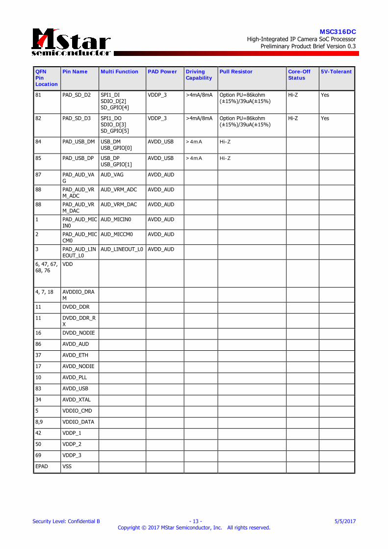
PIN CHARACTERISTICS QFN Pin Location
Pin Name Multi Function PAD Power Driving Capability
Pull Resistor Core-Off Status
5V-Tolerant
12 PAD_SAR_GPIO3
SAR_ASI3 SAR_GPIO[3]
AVDD_NODIE >4mA Hi-Z Hi-Z Yes
13 PAD_SAR_GPIO2
SAR_ASI2 SAR_GPIO[2]
AVDD_NODIE >4mA Hi-Z Hi-Z Yes
14 PAD_SAR_GPIO1
SAR_ASI1 SAR_GPIO[1]
AVDD_NODIE >4mA Hi-Z Hi-Z Yes
15 PAD_SAR_GPIO0
SAR_ASI0 SAR_GPIO[0]
AVDD_NODIE >4mA Hi-Z Hi-Z Yes
19 PAD_PM_SD_CDZ
SD_CDZ SD_CDZ_GPIO
AVDD_NODIE >4mA PU=86kohm (±15%)/39uA(±15%)
PU Yes
20 PAD_PM_IRIN IRIN IRIN_GPIO
AVDD_NODIE >4mA PU=86kohm (±15%)/39uA(±15%)
PU Yes
21 PAD_PM_RESET
HW_RESET AVDD_NODIE PD=64kohm (±15%)/52uA(±15%)
PD Yes
22 PAD_PM_UART_RX
UART_RX AVDD_NODIE >4mA PU=86kohm (±15%)/39uA(±15%)
PU Yes
23 PAD_PM_UART_TX
UART_TX AVDD_NODIE >4mA PU=86kohm (±15%)/39uA(±15%)
PU Yes
25 PAD_PM_GPIO4
GPIO_PM[4] AVDD_NODIE >4mA PU=86kohm (±15%)/39uA(±15%)
PU Yes
26 PAD_PM_SPI_CZ
SPI_CZ1 SPI_CZ2 SPI_GPIO[0]
AVDD_NODIE >4mA/8mA PU=86kohm (±15%)/39uA(±15%)
PU Yes
27 PAD_PM_SPI_DI
SPI_DI SPI_GPIO[2]
AVDD_NODIE >4mA/8mA PU=86kohm (±15%)/39uA(±15%)
PU Yes
28 PAD_PM_SPI_WPZ
SPI_WPZ SPI_GPIO[4]
AVDD_NODIE >4mA/8mA PU=86kohm (±15%)/39uA(±15%)
PU Yes
29 PAD_PM_SPI_DO
SPI_DO SPI_GPIO[3]
AVDD_NODIE >4mA/8mA PU=86kohm (±15%)/39uA(±15%)
PU Yes
30 PAD_PM_SPI_CK
SPI_CK SPI_GPIO[1]
AVDD_NODIE >4mA/8mA PD=64kohm (±15%)/52uA(±15%)
PD Yes
31 PAD_PM_SPI_HLD
SPI_HLDZ SPI_GPIO[5]
AVDD_NODIE >4mA/8mA PU=86kohm (±15%)/39uA(±15%)
PU Yes
32 PAD_PM_LED0 ETH_LED0 LED_GPIO[0]
AVDD_NODIE >4mA PD=64kohm (±15%)/52uA(±15%)
PD Yes
33 PAD_PM_LED1 ETH_LED1 LED_GPIO[1]
AVDD_NODIE >4mA PD=64kohm (±15%)/52uA(±15%)
PD Yes
35 PAD_XTAL_IN XTAL_IN AVDD_XTAL
36 PAD_XTAL_OUT
XTAL_OUT AVDD_XTAL
38 PAD_ETH_RN ETH_RN ETH_GPIO[0]
AVDD_ETH
39 PAD_ETH_RP ETH_RP ETH_GPIO[1]
AVDD_ETH
40 PAD_ETH_TN ETH_TN ETH_GPIO[2]
AVDD_ETH
41 PAD_ETH_TP ETH_TP ETH_GPIO[3]
AVDD_ETH
MSC316DC High-Integrated IP Camera SoC Processor
Preliminary Product Brief Version 0.3
Security Level: Confidential B - 10 - 5/5/2017 Copyright © 2017 MStar Semiconductor, Inc. All rights reserved.
QFN Pin Location
Pin Name Multi Function PAD Power Driving Capability
Pull Resistor Core-Off Status
5V-Tolerant
43 PAD_FUART_RX
FUART_RX UART0_RX EJ_TCK SPI0_CZ PWM0 FUART_GPIO[0]
VDDP_1 >4mA PU=86kohm (±15%)/39uA(±15%)
PU Yes
44 PAD_FUART_TX
FUART_TX UART0_TX EJ_TMS SPI0_CK PWM1 FUART_GPIO[1]
VDDP_1 >4mA PU=86kohm (±15%)/39uA(±15%)
PU Yes
45 PAD_FUART_CTS
FUART_CTS UART1_RX EJ_TDO SPI0_DI PWM2 FUART_GPIO[2]
VDDP_1 >4mA PU=86kohm (±15%)/39uA(±15%)
PU Yes
46 PAD_FUART_RTS
FUART_RTS UART1_TX EJ_TDI SPI0_DO PWM3 FUART_GPIO[3]
VDDP_1 >4mA PU=86kohm (±15%)/39uA(±15%)
PU Yes
48 PAD_I2C1_SCL
I2C1_SCL SR_SCL I2C1_GPIO[0]
VDDP_2 >4mA/8mA Option PU = 90kohm (+/-15%) Option PD = 64kohm (+/-15%)
PU No
49 PAD_I2C1_SDA
I2C1_SDA SR_SDA I2C1_GPIO[1]
VDDP_2 >4mA/8mA Option PU = 90kohm (+/-15%) Option PD = 64kohm (+/-15%)
PU No
51 PAD_SR_IO02 SR_D[9] SR_D[8] SR_D[4] SR_HS SR_D[2] CCIR_IN_D[0] SR_GPIO[2]
VDDP_2 >4mA/8mA Option PU = 90kohm (+/-15%) Option PD = 64kohm (+/-15%)
PU No
52 PAD_SR_IO03 SR_D[7] SR_D[6] SR_D[2] SR_D[0] SR_D[3] CCIR_IN_D[1] SR_GPIO[3]
VDDP_2 >4mA/8mA Option PU = 90kohm (+/-15%) Option PD = 64kohm (+/-15%)
PU No
53 PAD_SR_IO04 SR_PCK SR_D[4] SR_D[1] CCIR_IN_D[2] SR_GPIO[4]
VDDP_2 >4mA/8mA Option PU = 90kohm (+/-15%) Option PD = 64kohm (+/-15%)
PU No
54 PAD_SR_IO05 SR_D[1] SR_D[2] SR_D[0] SR_D[5] CCIR_IN_D[3] SR_GPIO[5]
VDDP_2 >4mA/8mA Option PU = 90kohm (+/-15%) Option PD = 64kohm (+/-15%)
PU No
MSC316DC High-Integrated IP Camera SoC Processor
Preliminary Product Brief Version 0.3
Security Level: Confidential B - 11 - 5/5/2017 Copyright © 2017 MStar Semiconductor, Inc. All rights reserved.
QFN Pin Location
Pin Name Multi Function PAD Power Driving Capability
Pull Resistor Core-Off Status
5V-Tolerant
55 PAD_SR_IO06 SR_D[0] SR_PCK SR_D[2] SR_D[3] SR_D[6] CCIR_IN_D[4] SR_GPIO[6]
VDDP_2 >4mA/8mA Option PU = 90kohm (+/-15%) Option PD = 64kohm (+/-15%)
PU No
56 PAD_SR_IO07 SR_D[3] SR_D[1] SR_PCK SR_D[9] SR_D[4] SR_D[7] CCIR_IN_D[5] SR_GPIO[7]
VDDP_2 >4mA/8mA Option PU = 90kohm (+/-15%) Option PD = 64kohm (+/-15%)
PU No
57 PAD_SR_IO08 SR_D[5] SR_D[0] SR_D[1] SR_D[3] SR_D[8] CCIR_IN_D[6] SR_GPIO[8]
VDDP_2 >4mA/8mA Option PU = 90kohm (+/-15%) Option PD = 64kohm (+/-15%)
PU No
58 PAD_SR_IO09 SR_D[4] SR_D[9] SR_D[7] SR_D[6] CCIR_IN_D[7] SR_GPIO[9]
VDDP_2 >4mA/8mA Option PU = 90kohm (+/-15%) Option PD = 64kohm (+/-15%)
PU No
59 PAD_SR_IO10 SR_D[6] SR_D[3] SR_D[5] SR_RST SR_MCK SR_D[10] CCIR_IN_D[8] SR_GPIO[10]
VDDP_2 >4mA/8mA Option PU = 90kohm (+/-15%) Option PD = 64kohm (+/-15%)
PU No
60 PAD_SR_IO11 SR_MCK SR_D[7] SR_D[3] SR_D[5] SR_D[11] CCIR_IN_D[9] SR_GPIO[11]
VDDP_2 >4mA/8mA Option PU = 90kohm (+/-15%) Option PD = 64kohm (+/-15%)
PU No
61 PAD_SR_IO12 SR_HS SR_RST SR_D[9] SR_VS SR_D[8] SR_PDN CCIR_IN_CLK SR_GPIO[12]
VDDP_2 >4mA/8mA Option PU = 90kohm (+/-15%) Option PD = 64kohm (+/-15%)
PU No
62 PAD_SR_IO13 SR_VS SR_D[5] SR_HS SR_D[9] SR_RST SR_GPIO[13]
VDDP_2 >4mA/8mA Option PU = 90kohm (+/-15%) Option PD = 64kohm (+/-15%)
PU No

MSC316DC High-Integrated IP Camera SoC Processor
Preliminary Product Brief Version 0.3
Security Level: Confidential B - 12 - 5/5/2017 Copyright © 2017 MStar Semiconductor, Inc. All rights reserved.
QFN Pin Location
Pin Name Multi Function PAD Power Driving Capability
Pull Resistor Core-Off Status
5V-Tolerant
63 PAD_SR_IO14 SR_D[8] SR_VS SR_PDN SR_D[10] SR_HS SR_GPIO[14]
VDDP_2 >4mA/8mA Option PU = 90kohm (+/-15%) Option PD = 64kohm (+/-15%)
PU No
64 PAD_SR_IO15 SR_D[2] SR_HS SR_MCK SR_D[11] SR_PCK SR_GPIO[15]
VDDP_2 >4mA/8mA Option PU = 90kohm (+/-15%) Option PD = 64kohm (+/-15%)
PU No
65 PAD_SR_IO16 SR_PDN SR_PCK SR_VS SR_GPIO[16]
VDDP_2 >4mA/8mA Option PU = 90kohm (+/-15%) Option PD = 64kohm (+/-15%)
PU No
66 PAD_SR_IO17 SR_RST SR_MCK SR_GPIO[17]
VDDP_2 >4mA/8mA Option PU = 90kohm (+/-15%) Option PD = 64kohm (+/-15%)
PU No
70 PAD_SPI0_CZ SPI0_CZ TTL_B[7] PWM4 SPI0_GPIO[0]
VDDP_3 >4mA/8mA/12mA/16mA
PU=86kohm (±15%)/39uA(±15%)
PU No
71 PAD_SPI0_CK SPI0_CK TTL_LCK PWM5 SPI0_GPIO[1]
VDDP_3 >4mA/8mA/12mA/16mA
PD=64kohm (±15%)/52uA(±15%)
PD No
72 PAD_SPI0_DI SPI0_DI TTL_LVSYNC PWM6 SPI0_GPIO[2]
VDDP_3 >4mA/8mA/12mA/16mA
PD=64kohm (±15%)/52uA(±15%)
PD No
73 PAD_SPI0_DO SPI0_DO TTL_LHSYNC PWM7 SPI0_GPIO[3]
VDDP_3 >4mA/8mA/12mA/16mA
PD=64kohm (±15%)/52uA(±15%)
PD No
74 PAD_PWM0 I2C0_SCL I2C1_SCL TTL_LDE PWM0 PWM_GPIO[0]
VDDP_3 >4mA/8mA PU=86kohm (±15%)/39uA(±15%)
PU Yes
75 PAD_PWM1 I2C0_SDA I2C1_SDA PWM1 PWM_GPIO[1]
VDDP_3 >4mA PU=86kohm (±15%)/39uA(±15%)
PU Yes
77 PAD_SD_CLK SDIO_CLK SD_GPIO[0]
VDDP_3 >4mA/8mA PD=64kohm (±15%)/52uA(±15%)
PD Yes
78 PAD_SD_CMD SDIO_CMD SD_GPIO[1]
VDDP_3 >4mA/8mA Option PU=86kohm (±15%)/39uA(±15%)
Hi-Z Yes
79 PAD_SD_D0 SPI1_CZ SDIO_D[0] SD_GPIO[2]
VDDP_3 >4mA/8mA Option PU=86kohm (±15%)/39uA(±15%)
Hi-Z Yes
80 PAD_SD_D1 SPI1_CK SDIO_D[1] SD_GPIO[3]
VDDP_3 >4mA/8mA Option PU=86kohm (±15%)/39uA(±15%)
Hi-Z Yes
MSC316DC High-Integrated IP Camera SoC Processor
Preliminary Product Brief Version 0.3
Security Level: Confidential B - 13 - 5/5/2017 Copyright © 2017 MStar Semiconductor, Inc. All rights reserved.
QFN Pin Location
Pin Name Multi Function PAD Power Driving Capability
Pull Resistor Core-Off Status
5V-Tolerant
81 PAD_SD_D2 SPI1_DI SDIO_D[2] SD_GPIO[4]
VDDP_3 >4mA/8mA Option PU=86kohm (±15%)/39uA(±15%)
Hi-Z Yes
82 PAD_SD_D3 SPI1_DO SDIO_D[3] SD_GPIO[5]
VDDP_3 >4mA/8mA Option PU=86kohm (±15%)/39uA(±15%)
Hi-Z Yes
84 PAD_USB_DM USB_DM USB_GPIO[0]
AVDD_USB >4mA Hi-Z
85 PAD_USB_DP USB_DP USB_GPIO[1]
AVDD_USB >4mA Hi-Z
87 PAD_AUD_VAG
AUD_VAG AVDD_AUD
88 PAD_AUD_VRM_ADC
AUD_VRM_ADC AVDD_AUD
88 PAD_AUD_VRM_DAC
AUD_VRM_DAC AVDD_AUD
1 PAD_AUD_MICIN0
AUD_MICIN0 AVDD_AUD
2 PAD_AUD_MICCM0
AUD_MICCM0 AVDD_AUD
3 PAD_AUD_LINEOUT_L0
AUD_LINEOUT_L0 AVDD_AUD
6, 47, 67, 68, 76
VDD
4, 7, 18 AVDDIO_DRAM
11 DVDD_DDR
11 DVDD_DDR_RX
16 DVDD_NODIE
86 AVDD_AUD
37 AVDD_ETH
17 AVDD_NODIE
10 AVDD_PLL
83 AVDD_USB
34 AVDD_XTAL
5 VDDIO_CMD
8,9 VDDIO_DATA
42 VDDP_1
50 VDDP_2
69 VDDP_3
EPAD VSS
MSC316DC High-Integrated IP Camera SoC Processor
Preliminary Product Brief Version 0.3
Security Level: Confidential B - 14 - 5/5/2017 Copyright © 2017 MStar Semiconductor, Inc. All rights reserved.
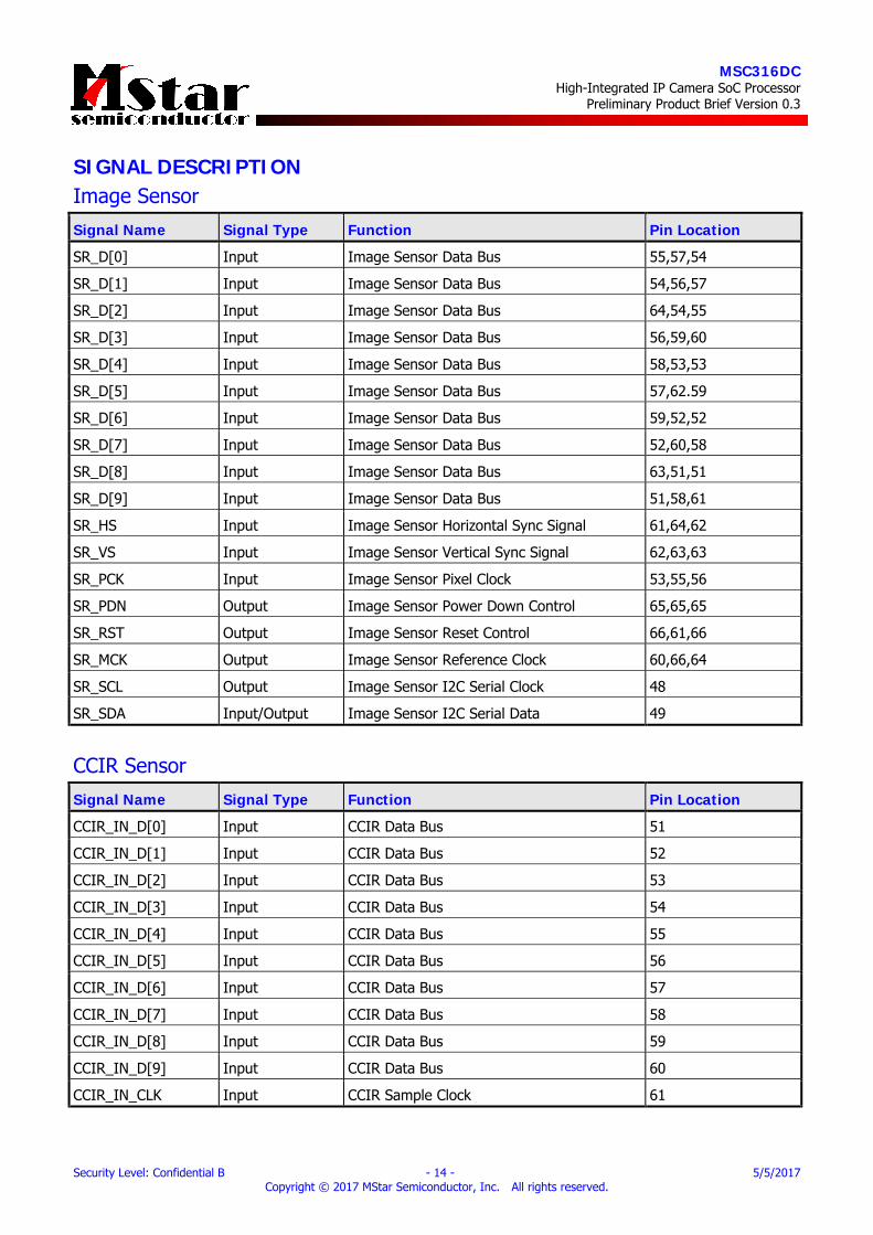
SIGNAL DESCRIPTION Image Sensor Signal Name Signal Type Function Pin Location
SR_D[0] Input Image Sensor Data Bus 55,57,54
SR_D[1] Input Image Sensor Data Bus 54,56,57
SR_D[2] Input Image Sensor Data Bus 64,54,55
SR_D[3] Input Image Sensor Data Bus 56,59,60
SR_D[4] Input Image Sensor Data Bus 58,53,53
SR_D[5] Input Image Sensor Data Bus 57,62.59
SR_D[6] Input Image Sensor Data Bus 59,52,52
SR_D[7] Input Image Sensor Data Bus 52,60,58
SR_D[8] Input Image Sensor Data Bus 63,51,51
SR_D[9] Input Image Sensor Data Bus 51,58,61
SR_HS Input Image Sensor Horizontal Sync Signal 61,64,62
SR_VS Input Image Sensor Vertical Sync Signal 62,63,63
SR_PCK Input Image Sensor Pixel Clock 53,55,56
SR_PDN Output Image Sensor Power Down Control 65,65,65
SR_RST Output Image Sensor Reset Control 66,61,66
SR_MCK Output Image Sensor Reference Clock 60,66,64
SR_SCL Output Image Sensor I2C Serial Clock 48
SR_SDA Input/Output Image Sensor I2C Serial Data 49
CCIR Sensor Signal Name Signal Type Function Pin Location
CCIR_IN_D[0] Input CCIR Data Bus 51
CCIR_IN_D[1] Input CCIR Data Bus 52
CCIR_IN_D[2] Input CCIR Data Bus 53
CCIR_IN_D[3] Input CCIR Data Bus 54
CCIR_IN_D[4] Input CCIR Data Bus 55
CCIR_IN_D[5] Input CCIR Data Bus 56
CCIR_IN_D[6] Input CCIR Data Bus 57
CCIR_IN_D[7] Input CCIR Data Bus 58
CCIR_IN_D[8] Input CCIR Data Bus 59
CCIR_IN_D[9] Input CCIR Data Bus 60
CCIR_IN_CLK Input CCIR Sample Clock 61

MSC316DC High-Integrated IP Camera SoC Processor
Preliminary Product Brief Version 0.3
Security Level: Confidential B - 15 - 5/5/2017 Copyright © 2017 MStar Semiconductor, Inc. All rights reserved.
Audio Interface Signal Name Signal Type Function Pin Location
AUD_LINEOUT_L0 Output Audio Left Channel Line Output 3
AUD_VAG Output Audio Reference Voltage from 1/2 AVDD_AUD
87
AUD_VRM_ADC Input Audio Reference Voltage for ADC 88
AUD_VRM_DAC Input Audio Reference Voltage for DAC 88
AUD_MICIN0 Input Audio Left Channel Microphone Postive Input 1
AUD_MICCM0 Input Audio Left Channel Microphone Negative Input
2
10/100 Ethernet Interface Signal Name Signal Type Function Pin Location
ETH_RN Input 10/100 Ethernet Negative Receiving Input 38
ETH_RP Input 10/100 Ethernet Positive Receiving Input 39
ETH_TN Output 10/100 Ethernet Negative Transmitting Output
40
ETH_TP Output 10/100 Ethernet Positive Transmitting Output 41
SDIO Interface Signal Name Signal Type Function Pin Location
SDIO_CLK Output SDIO 2.0 Clock 77
SDIO_CMD Output SDIO 2.0 Command 78
SDIO_D[0] Input/Output SDIO 2.0 Data Bus 79
SDIO_D[1] Input/Output SDIO 2.0 Data Bus 80
SDIO_D[2] Input/Output SDIO 2.0 Data Bus 81
SDIO_D[3] Input/Output SDIO 2.0 Data Bus 82
SD_CDZ Input SD Card Detect (active low) 19
SPI Flash Interface Signal Name Signal Type Function Pin Location
SPI_CK Output SPI Flash Clock 30
SPI_CZ1 Output SPI Flash Chip Select 1 (active low) 26
SPI_DI Output SPI Flash Serial DataTo Device 27
SPI_DO Input SPI Flash Serial Data From Device 29
SPI_WPZ Output SPI Flash Write Protect Control (active low) 28
MSC316DC High-Integrated IP Camera SoC Processor
Preliminary Product Brief Version 0.3
Security Level: Confidential B - 16 - 5/5/2017 Copyright © 2017 MStar Semiconductor, Inc. All rights reserved.
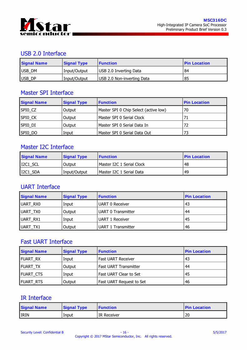
USB 2.0 Interface Signal Name Signal Type Function Pin Location
USB_DM Input/Output USB 2.0 Inverting Data 84
USB_DP Input/Output USB 2.0 Non-inverting Data 85
Master SPI Interface Signal Name Signal Type Function Pin Location
SPI0_CZ Output Master SPI 0 Chip Select (active low) 70
SPI0_CK Output Master SPI 0 Serial Clock 71
SPI0_DI Output Master SPI 0 Serial Data In 72
SPI0_DO Input Master SPI 0 Serial Data Out 73
Master I2C Interface Signal Name Signal Type Function Pin Location
I2C1_SCL Output Master I2C 1 Serial Clock 48
I2C1_SDA Input/Output Master I2C 1 Serial Data 49
UART Interface Signal Name Signal Type Function Pin Location
UART_RX0 Input UART 0 Receiver 43
UART_TX0 Output UART 0 Transmitter 44
UART_RX1 Input UART 1 Receiver 45
UART_TX1 Output UART 1 Transmitter 46
Fast UART Interface Signal Name Signal Type Function Pin Location
FUART_RX Input Fast UART Receiver 43
FUART_TX Output Fast UART Transmitter 44
FUART_CTS Input Fast UART Clear to Set 45
FUART_RTS Output Fast UART Request to Set 46
IR Interface Signal Name Signal Type Function Pin Location
IRIN Input IR Receiver 20
MSC316DC High-Integrated IP Camera SoC Processor
Preliminary Product Brief Version 0.3
Security Level: Confidential B - 17 - 5/5/2017 Copyright © 2017 MStar Semiconductor, Inc. All rights reserved.
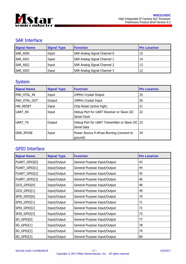
SAR Interface Signal Name Signal Type Function Pin Location
SAR_ASI0 Input SAR Analog Signal Channel 0 15
SAR_ASI1 Input SAR Analog Signal Channel 1 14
SAR_ASI2 Input SAR Analog Signal Channel 2 13
SAR_ASI3 Input SAR Analog Signal Channel 3 12
System Signal Name Signal Type Function Pin Location
PAD_XTAL_IN Input 24MHz Crystal Output 35
PAD_XTAL_OUT Output 24MHz Crystal Input 36
HW_RESET Input Chip Reset (active high) 21
UART_RX Input Debug Port for UART Receiver or Slave I2C Serial Clock
22
UART_TX Output Debug Port for UART Transmitter or Slave I2C Serial Data
23
GND_EFUSE Input Power Source if eFuse Burning (connect to ground)
24
GPIO Interface Signal Name Signal Type Function Pin Location
FUART_GPIO[0] Input/Output General Purpose Input/Output 43
FUART_GPIO[1] Input/Output General Purpose Input/Output 44
FUART_GPIO[2] Input/Output General Purpose Input/Output 45
FUART_GPIO[3] Input/Output General Purpose Input/Output 46
I2C0_GPIO[0] Input/Output General Purpose Input/Output 48
I2C0_GPIO[1] Input/Output General Purpose Input/Output 49
SPI0_GPIO[0] Input/Output General Purpose Input/Output 70
SPI0_GPIO[1] Input/Output General Purpose Input/Output 71
SPI0_GPIO[2] Input/Output General Purpose Input/Output 72
SPI0_GPIO[3] Input/Output General Purpose Input/Output 73
SD_GPIO[0] Input/Output General Purpose Input/Output 77
SD_GPIO[1] Input/Output General Purpose Input/Output 78
SD_GPIO[2] Input/Output General Purpose Input/Output 79
SD_GPIO[3] Input/Output General Purpose Input/Output 80
MSC316DC High-Integrated IP Camera SoC Processor
Preliminary Product Brief Version 0.3
Security Level: Confidential B - 18 - 5/5/2017 Copyright © 2017 MStar Semiconductor, Inc. All rights reserved.
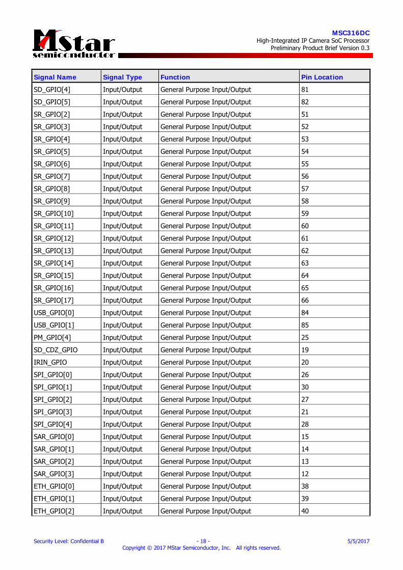
Signal Name Signal Type Function Pin Location
SD_GPIO[4] Input/Output General Purpose Input/Output 81
SD_GPIO[5] Input/Output General Purpose Input/Output 82
SR_GPIO[2] Input/Output General Purpose Input/Output 51
SR_GPIO[3] Input/Output General Purpose Input/Output 52
SR_GPIO[4] Input/Output General Purpose Input/Output 53
SR_GPIO[5] Input/Output General Purpose Input/Output 54
SR_GPIO[6] Input/Output General Purpose Input/Output 55
SR_GPIO[7] Input/Output General Purpose Input/Output 56
SR_GPIO[8] Input/Output General Purpose Input/Output 57
SR_GPIO[9] Input/Output General Purpose Input/Output 58
SR_GPIO[10] Input/Output General Purpose Input/Output 59
SR_GPIO[11] Input/Output General Purpose Input/Output 60
SR_GPIO[12] Input/Output General Purpose Input/Output 61
SR_GPIO[13] Input/Output General Purpose Input/Output 62
SR_GPIO[14] Input/Output General Purpose Input/Output 63
SR_GPIO[15] Input/Output General Purpose Input/Output 64
SR_GPIO[16] Input/Output General Purpose Input/Output 65
SR_GPIO[17] Input/Output General Purpose Input/Output 66
USB_GPIO[0] Input/Output General Purpose Input/Output 84
USB_GPIO[1] Input/Output General Purpose Input/Output 85
PM_GPIO[4] Input/Output General Purpose Input/Output 25
SD_CDZ_GPIO Input/Output General Purpose Input/Output 19
IRIN_GPIO Input/Output General Purpose Input/Output 20
SPI_GPIO[0] Input/Output General Purpose Input/Output 26
SPI_GPIO[1] Input/Output General Purpose Input/Output 30
SPI_GPIO[2] Input/Output General Purpose Input/Output 27
SPI_GPIO[3] Input/Output General Purpose Input/Output 21
SPI_GPIO[4] Input/Output General Purpose Input/Output 28
SAR_GPIO[0] Input/Output General Purpose Input/Output 15
SAR_GPIO[1] Input/Output General Purpose Input/Output 14
SAR_GPIO[2] Input/Output General Purpose Input/Output 13
SAR_GPIO[3] Input/Output General Purpose Input/Output 12
ETH_GPIO[0] Input/Output General Purpose Input/Output 38
ETH_GPIO[1] Input/Output General Purpose Input/Output 39
ETH_GPIO[2] Input/Output General Purpose Input/Output 40
MSC316DC High-Integrated IP Camera SoC Processor
Preliminary Product Brief Version 0.3
Security Level: Confidential B - 19 - 5/5/2017 Copyright © 2017 MStar Semiconductor, Inc. All rights reserved.
Signal Name Signal Type Function Pin Location
ETH_GPIO[3] Input/Output General Purpose Input/Output 41
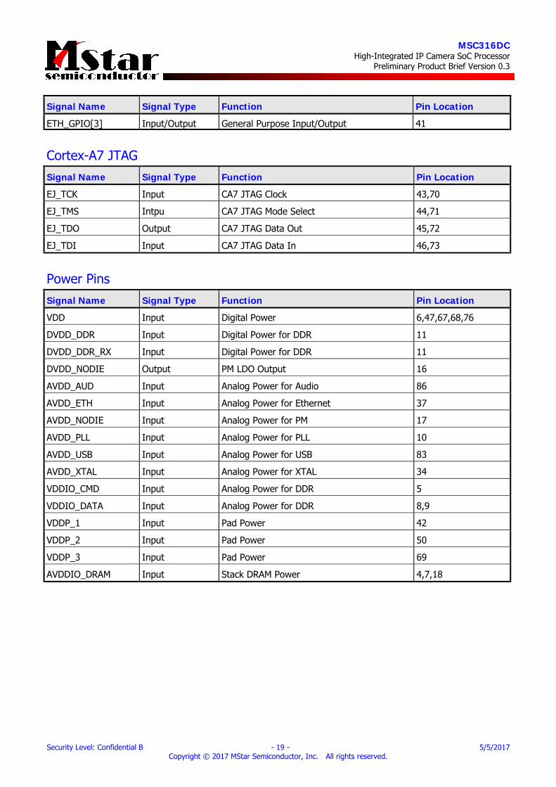
Cortex-A7 JTAG Signal Name Signal Type Function Pin Location
EJ_TCK Input CA7 JTAG Clock 43,70
EJ_TMS Intpu CA7 JTAG Mode Select 44,71
EJ_TDO Output CA7 JTAG Data Out 45,72
EJ_TDI Input CA7 JTAG Data In 46,73
Power Pins Signal Name Signal Type Function Pin Location
VDD Input Digital Power 6,47,67,68,76
DVDD_DDR Input Digital Power for DDR 11
DVDD_DDR_RX Input Digital Power for DDR 11
DVDD_NODIE Output PM LDO Output 16
AVDD_AUD Input Analog Power for Audio 86
AVDD_ETH Input Analog Power for Ethernet 37
AVDD_NODIE Input Analog Power for PM 17
AVDD_PLL Input Analog Power for PLL 10
AVDD_USB Input Analog Power for USB 83
AVDD_XTAL Input Analog Power for XTAL 34
VDDIO_CMD Input Analog Power for DDR 5
VDDIO_DATA Input Analog Power for DDR 8,9
VDDP_1 Input Pad Power 42
VDDP_2 Input Pad Power 50
VDDP_3 Input Pad Power 69
AVDDIO_DRAM Input Stack DRAM Power 4,7,18
MSC316DC High-Integrated IP Camera SoC Processor
Preliminary Product Brief Version 0.3
Security Level: Confidential B - 20 - 5/5/2017 Copyright © 2017 MStar Semiconductor, Inc. All rights reserved.
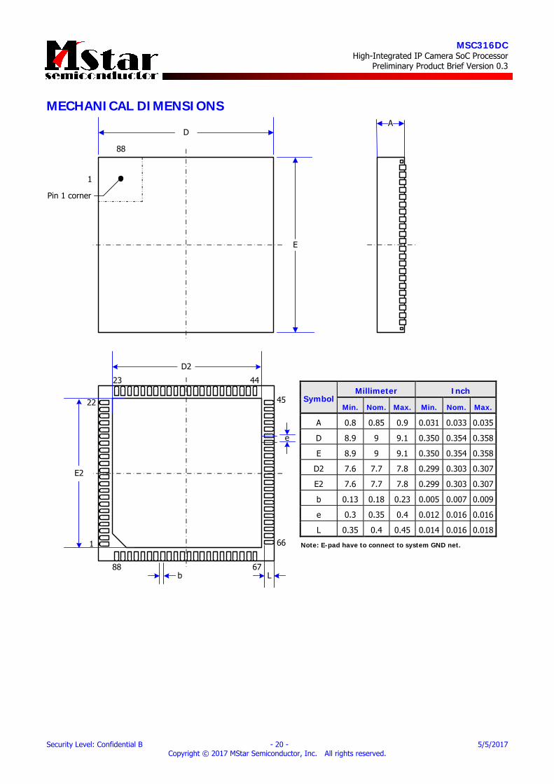
MECHANICAL DIMENSIONS
DA
45
e
b
66
Pin 1 corner
1
88
22
1
88 67
23 44
E
Symbol Millimeter Inch
Min. Nom. Max. Min. Nom. Max.
A 0.8 0.85 0.9 0.031 0.033 0.035
D 8.9 9 9.1 0.350 0.354 0.358
E 8.9 9 9.1 0.350 0.354 0.358
D2 7.6 7.7 7.8 0.299 0.303 0.307
E2 7.6 7.7 7.8 0.299 0.303 0.307
b 0.13 0.18 0.23 0.005 0.007 0.009
e 0.3 0.35 0.4 0.012 0.016 0.016
L 0.35 0.4 0.45 0.014 0.016 0.018
Note: E-pad have to connect to system GND net.
D2
E2
L

MSC316DC High-Integrated IP Camera SoC Processor
Preliminary Product Brief Version 0.3
Security Level: Confidential B - 21 - 5/5/2017 Copyright © 2017 MStar Semiconductor, Inc. All rights reserved.
ELECTRICAL SPECIFICATIONS Interface Characteristics Parameter Symbol Min. Typ. Max. Unit
DIGITAL INPUTS Input Voltage, High Input Voltage, Low Input Current, High Input Current, Low Input Capacitance
VIH
VIL
IIH
IIL
2.5
5
0.8 -1.0 1.0
V V uA uA pF
DIGITAL OUTPUTS Output Voltage, High Output Voltage, Low
VOH
VOL
VDDP-0.1Note
0.1
V V
SAR ADC Input 0 VVDD_33 V
AUDIO OUTPUTS Line-Out
2.54
Vp-p
Note: 1. VDDP can be VVDD_33, VVDD_15
2. 0.9Vrms @10Kohm load
Recommended Operating Conditions Parameter Symbol Min Typ. Max. Unit
3.3V Supply Voltage VVDD_33 3.3 V
1.5V Supply Voltage (DDR III) VVDD_15 1.5 V
Core Power Supply Voltage (Core) VVDD_core 0.87 0.9 V
Ambient Operation Temperature TA -40 85 °C
Junction Temperature TJ 125 °C
Absolute Maximum Ratings Parameter Symbol Min Typ. Max. Unit
3.3V Supply Voltage VVDD_33 3.63 V
1.5V Supply Voltage (DDR III) VVDD_15 1.65 V
Core Power Supply Voltage (Core) VVDD_core 1.26 V
Storage Temperature TSTG -40 150 °C
Note: Stresses above those listed in Absolute Maximum Ratings may cause permanent damage to the device. This is a stress
rating only and does not imply functional operation of device. Exposure to absolute maximum ratings for extended
periods may affect device reliability.
MSC316DC High-Integrated IP Camera SoC Processor
Preliminary Product Brief Version 0.3
Security Level: Confidential B - 22 - 5/5/2017 Copyright © 2017 MStar Semiconductor, Inc. All rights reserved.
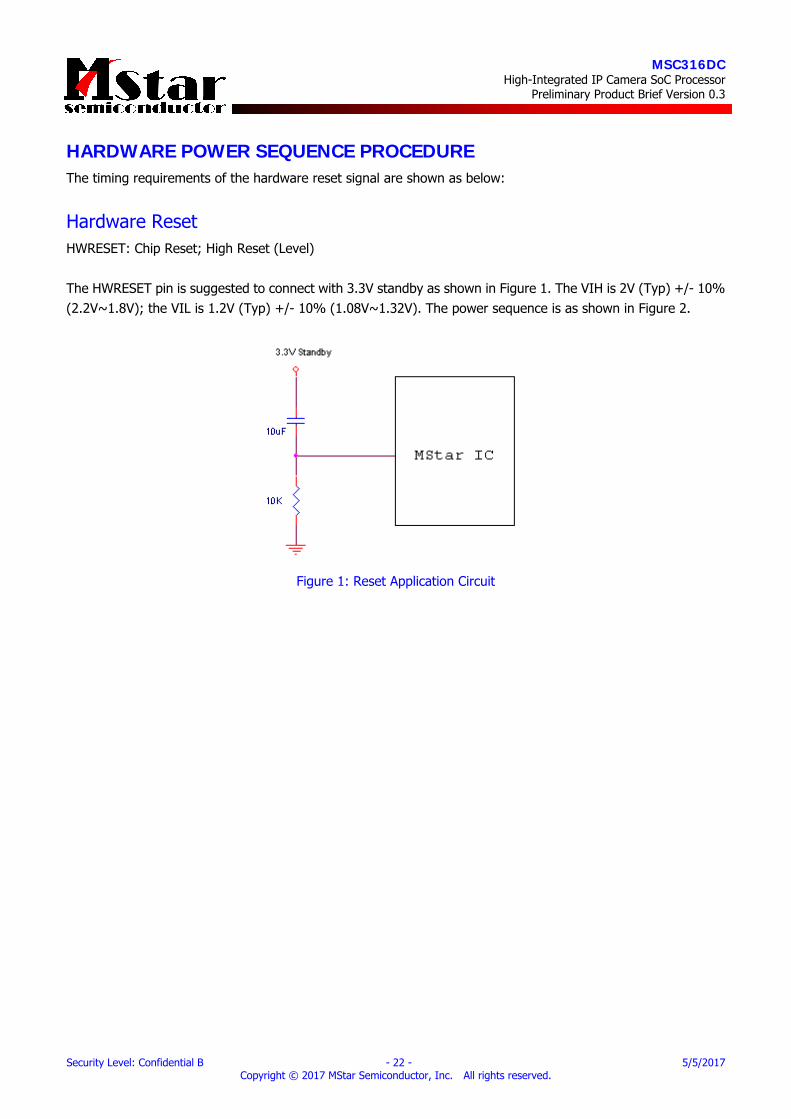
HARDWARE POWER SEQUENCE PROCEDURE The timing requirements of the hardware reset signal are shown as below:
Hardware Reset HWRESET: Chip Reset; High Reset (Level) The HWRESET pin is suggested to connect with 3.3V standby as shown in Figure 1. The VIH is 2V (Typ) +/- 10% (2.2V~1.8V); the VIL is 1.2V (Typ) +/- 10% (1.08V~1.32V). The power sequence is as shown in Figure 2.
Figure 1: Reset Application Circuit
MSC316DC High-Integrated IP Camera SoC Processor
Preliminary Product Brief Version 0.3
Security Level: Confidential B - 23 - 5/5/2017 Copyright © 2017 MStar Semiconductor, Inc. All rights reserved.
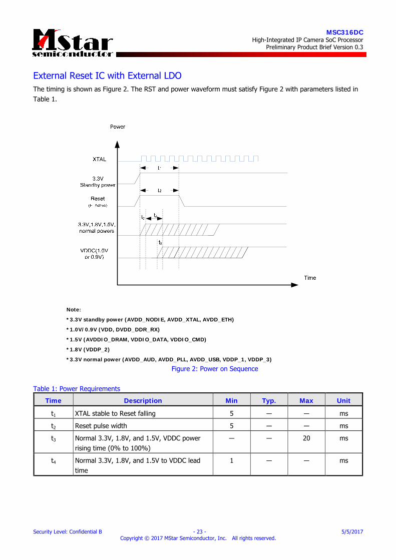
External Reset IC with External LDO The timing is shown as Figure 2. The RST and power waveform must satisfy Figure 2 with parameters listed in Table 1.
Note:
*3.3V standby power (AVDD_NODIE, AVDD_XTAL, AVDD_ETH)
*1.0V/0.9V (VDD, DVDD_DDR_RX)
*1.5V (AVDDIO_DRAM, VDDIO_DATA, VDDIO_CMD)
*1.8V (VDDP_2)
*3.3V normal power (AVDD_AUD, AVDD_PLL, AVDD_USB, VDDP_1, VDDP_3)
Figure 2: Power on Sequence Table 1: Power Requirements
Time Description Min Typ. Max Unit
t1 XTAL stable to Reset falling 5 ― ― ms
t2 Reset pulse width 5 ― ― ms
t3 Normal 3.3V, 1.8V, and 1.5V, VDDC power rising time (0% to 100%)
― ― 20 ms
t4 Normal 3.3V, 1.8V, and 1.5V to VDDC lead time
1 ― ― ms
MSC316DC High-Integrated IP Camera SoC Processor
Preliminary Product Brief Version 0.3
Security Level: Confidential B - 24 - 5/5/2017 Copyright © 2017 MStar Semiconductor, Inc. All rights reserved.
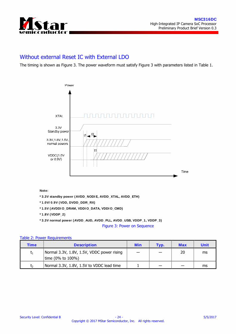
Without external Reset IC with External LDO The timing is shown as Figure 3. The power waveform must satisfy Figure 3 with parameters listed in Table 1.
Note:
*3.3V standby power (AVDD_NODIE, AVDD_XTAL, AVDD_ETH)
*1.0V/0.9V (VDD, DVDD_DDR_RX)
*1.5V (AVDDIO_DRAM, VDDIO_DATA, VDDIO_CMD)
*1.8V (VDDP_2)
*3.3V normal power (AVDD_AUD, AVDD_PLL, AVDD_USB, VDDP_1, VDDP_3)
Figure 3: Power on Sequence Table 2: Power Requirements
Time Description Min Typ. Max Unit
t1 Normal 3.3V, 1.8V, 1.5V, VDDC power rising time (0% to 100%)
― ― 20 ms
t2 Normal 3.3V, 1.8V, 1.5V to VDDC lead time 1 ― ― ms
MSC316DC High-Integrated IP Camera SoC Processor
Preliminary Product Brief Version 0.3
Security Level: Confidential B - 25 - 5/5/2017 Copyright © 2017 MStar Semiconductor, Inc. All rights reserved.
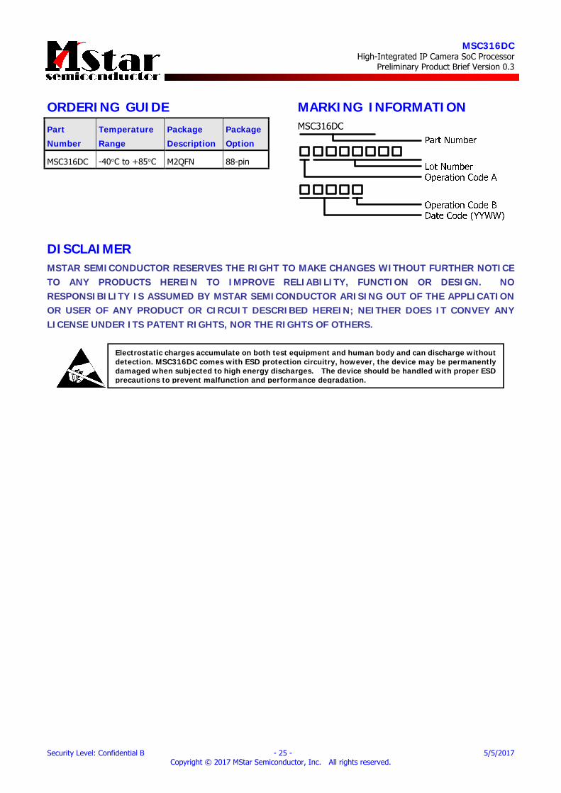
ORDERING GUIDE Part
Number
Temperature
Range
Package
Description
Package
Option
MSC316DC -40°C to +85°C M2QFN 88-pin
MARKING INFORMATION MSC316DC
DISCLAIMER MSTAR SEMICONDUCTOR RESERVES THE RIGHT TO MAKE CHANGES WITHOUT FURTHER NOTICE TO ANY PRODUCTS HEREIN TO IMPROVE RELIABILITY, FUNCTION OR DESIGN. NO RESPONSIBILITY IS ASSUMED BY MSTAR SEMICONDUCTOR ARISING OUT OF THE APPLICATION OR USER OF ANY PRODUCT OR CIRCUIT DESCRIBED HEREIN; NEITHER DOES IT CONVEY ANY LICENSE UNDER ITS PATENT RIGHTS, NOR THE RIGHTS OF OTHERS.
Electrostatic charges accumulate on both test equipment and human body and can discharge without detection. MSC316DC comes with ESD protection circuitry, however, the device may be permanently damaged when subjected to high energy discharges. The device should be handled with proper ESD precautions to prevent malfunction and performance degradation.


![[Tutorial] NoC the Next Generation of Multi-Processor SoC](https://img.pdfslide.us/doc/110x75/55cf9bb1550346d033a70a13/tutorial-noc-the-next-generation-of-multi-processor-soc.jpg)