Embed Size (px)
Citation preview

Do not exceed the operating input power level, voltagelevel, current level, and signal type that is appropriate forthe instrument being used. Refer to your instrument’s op-eration manual for safe operating practices and devicelimitations.
Electrostatic Discharge (ESD) can damage the highlysensitive circuits in the instrument. ESD is most likely tooccur as test devices are being connected to, or discon-nected from, the instrument’s front and rear panel portsand connectors. You can protect the instrument and testdevices by wearing a static-discharge wristband. Alterna-tively, you can ground yourself to discharge any staticcharge by touching the outer chassis of the grounded in-strument before touching the instrument’s front and rearpanel ports and connectors. Avoid touching the test portcenter conductors unless you are properly grounded andhave eliminated the possibility of static discharge.
Repair of damage that is found to be caused by electro-static discharge is not covered under warranty.
Caution


MS462XXVECTOR NETWORK MEASUREMENT SYSTEM
MAINTENANCE MANUAL
P/N: 10410-00205REVISION: J
PRINTED: APRIL 2012COPYRIGHT 2004 - 2012 ANRITSU CO.
490 JARVIS DRIVE � MORGAN HILL, CA 95037-2809

WARRANTYThe Anritsu product(s) listed on the title page is (are) warranted against defects in materials andworkmanship for three years from the date of shipment.
Anritsu's obligation covers repairing or replacing products which prove to be defective during thewarranty period. Buyers shall prepay transportation charges for equipment returned to Anritsu forwarranty repairs. Obligation is limited to the original purchaser. Anritsu is not liable for consequentialdamages.
LIMITATION OF WARRANTYThe foregoing warranty does not apply to Anritsu connectors that have failed due to normal wear.Also, the warranty does not apply to defects resulting from improper or inadequate maintenance bythe Buyer, unauthorized modification or misuse, or operation outside of the environmentalspecifications of the product. No other warranty is expressed or implied, and the remedies providedherein are the Buyer's sole and exclusive remedies.
TRADEMARK ACKNOWLEDGMENTSV Connector and K Connector are registered trademarks of Anritsu Company.HP 437B, HP 438A, DeskJet, and LaserJet are registered trademarks of Hewlett-Packard Company.GPC-7 is a registered trademark of Amphenol Corporation.Microsoft Excel, Notepad, and Windows are trademarks of Microsoft Corporation.
NOTICEAnritsu Company has prepared this manual for use by Anritsu Company personnel and customers asa guide for the proper installation, operation and maintenance of Anritsu Company equipment andcomputer programs. The drawings, specifications, and information contained herein are the propertyof Anritsu Company, and any unauthorized use or disclosure of these drawings, specifications, andinformation is prohibited; they shall not be reproduced, copied, or used in whole or in part as thebasis for manufacture or sale of the equipment or software programs without the prior writtenconsent of Anritsu Company.


Safety Symbols
To prevent the risk of personal injury or loss related to equipment malfunction, Anritsu Company uses thefollowing symbols to indicate safety-related information. For your own safety, please read this informationcarefully BEFORE operating the equipment.
Symbols Used in Manuals
DANGER Indicates a very dangerous procedure that could result in serious in-jury or death if not performed properly.
WARNING Indicates a hazardous procedure that could result in serious injury ordeath if not performed properly.
CAUTION Indicates a hazardous procedure or danger that could result in light-to-severe injury, or loss related to equipment malfunction, if properprecautions are not taken.
Safety Symbols Used on Equipment and in ManualsThe following safety symbols are used inside or on the equipment near operation locations to provide infor-mation about safety items and operation precautions. Ensure that you clearly understand the meanings ofthe symbols and take the necessary precautions BEFORE operating the equipment.
Some or all of the following five symbols may or may not be used on all Anritsu equipment. In addition, theremay be other labels attached to products that are not shown in the diagrams in this manual.
This symbol indicates a prohibited operation. The prohibited operationis indicated symbolically in or near the barred circle.
This symbol indicates a compulsory safety precaution. The requiredoperation is indicated symbolically in or near the circle.
This symbol indicates warning or caution. The contents are indicatedsymbolically in or near the triangle.
This symbol indicates a note. The contents are described in the box.
These symbols indicate that the marked part should be recycled.
MS462XX MM SAFETY-1

SAFETY-2 MS462XX MM
When supplying AC power to this equipment, connect the accessory 3-pinpower cord to a 3-pin grounded power outlet. If a grounded 3-pin outlet isnot available, use a conversion adapter and ground the green wire, orconnect the frame ground on the rear panel of the equipment to ground. Ifpower is supplied without grounding the equipment, there is a risk of re-ceiving a severe or fatal electric shock.
WARNING
This equipment cannot be repaired by the operator. DO NOT attempt to re-move the equipment covers or to disassemble internal components. Onlyqualified service technicians with a knowledge of electrical fire and shockhazards should service this equipment. There are high-voltage parts in thisequipment presenting a risk of severe injury or fatal electric shock to un-trained personnel. In addition, there is a risk of damage to precision com-ponents.
WARNING
Repair
For SafetyWARNING
Always refer to the operation manual when working near locations atwhich the alert mark, shown on the left, is attached. If the operation, etc.,is performed without heeding the advice in the operation manual, there isa risk of personal injury. In addition, the equipment performance may bereduced.Moreover, this alert mark is sometimes used with other marks and descrip-tions indicating other dangers.
If this equipment is used in a manner not specified by the manufacturer,the protection provided by the equipment may be impaired.
WARNING

Table of Contents, Narrative
Chapter 1—General Service InformationThis chapter familiarizes the user with the basic MS462XX Vector Network Measurement System.Included is information about related manuals, available models and options, preventive mainte-nance, recommended test equipment, replaceable assembly part numbers, and customer servicecontact information.
Chapter 2—Theory of OperationThis chapter provides a brief overview of the functional assemblies and major parts that comprisea typical MS462XX Vector Network Measurement System. It also briefly describes the operation ofeach major assembly and includes system block diagrams.
Chapter 3—Operational Performance TestsThis chapter provides general operational tests for all instruments with most of the availableoptions.
Chapter 4—System Performance VerificationThis chapter provides performance verification procedures for all non-C models.
Chapter 5—AdjustmentsThis chapter provides calibration procedures. Procedures include 10 MHz calibration, ALC adjust-ment, Back-end calibration, and Noise Source Internal Through Path characterization.
Chapter 6—TroubleshootingThis chapter provides information for troubleshooting MS462XX Vector Network MeasurementSystem. The troubleshooting procedures contained in this chapter support fault isolation down to areplaceable subassembly.
Chapter 7—Removal and Replacement ProceduresThis chapter describes how to gain access to all of the major assemblies and major parts for trou-bleshooting and/or replacement.
Appendix A—Connector Care and HandlingThis appendix provides information on the proper care and handling of RF sensor connectors.
Appendix B—Performance SpecificationsThis appendix contains performance specifications.
Subject Index
MS462XX MM i/ii


Table of Contents
Chapter 1 General Information
1-1 SCOPE OF THIS MANUAL . . . . . . . . . . . . . . . . . . . . . . . . . . . . . . 1-3
1-2 INTRODUCTION . . . . . . . . . . . . . . . . . . . . . . . . . . . . . . . . . . . 1-3
1-3 RELATED MANUALS. . . . . . . . . . . . . . . . . . . . . . . . . . . . . . . . . 1-3
1-4 MODELS . . . . . . . . . . . . . . . . . . . . . . . . . . . . . . . . . . . . . . . . 1-3
1-5 OPTIONS. . . . . . . . . . . . . . . . . . . . . . . . . . . . . . . . . . . . . . . . 1-4
1-6 IDENTIFICATION NUMBER. . . . . . . . . . . . . . . . . . . . . . . . . . . . . 1-4
1-7 SERVICE POLICY. . . . . . . . . . . . . . . . . . . . . . . . . . . . . . . . . . . 1-4
1-8 SPARE PARTS LISTING . . . . . . . . . . . . . . . . . . . . . . . . . . . . . . . 1-5
1-9 ASSEMBLY EXCHANGE PROGRAM . . . . . . . . . . . . . . . . . . . . . . . . 1-7
1-10 PREVENTIVE MAINTENANCE . . . . . . . . . . . . . . . . . . . . . . . . . . . 1-7
1-11 RECOMMENDED TEST EQUIPMENT . . . . . . . . . . . . . . . . . . . . . . . 1-7
1-12 CONVENTIONS . . . . . . . . . . . . . . . . . . . . . . . . . . . . . . . . . . . 1-10
1-13 COMPONENT HANDLING . . . . . . . . . . . . . . . . . . . . . . . . . . . . . 1-11
1-14 SERVICE CENTERS . . . . . . . . . . . . . . . . . . . . . . . . . . . . . . . . . 1-13
Chapter 2 Theory of Operation
2-1 INTRODUCTION . . . . . . . . . . . . . . . . . . . . . . . . . . . . . . . . . . . 2-3
2-2 SYSTEM OVERVIEW . . . . . . . . . . . . . . . . . . . . . . . . . . . . . . . . . 2-3
2-3 SOURCE MODULE . . . . . . . . . . . . . . . . . . . . . . . . . . . . . . . . . . 2-4Digital Interface . . . . . . . . . . . . . . . . . . . . . . . . . . . . . . . . . . 2-5Main Oscillator Loops . . . . . . . . . . . . . . . . . . . . . . . . . . . . . . . 2-5Offset Oscillator Loops . . . . . . . . . . . . . . . . . . . . . . . . . . . . . . 2-5DDS Reference Clock . . . . . . . . . . . . . . . . . . . . . . . . . . . . . . . 2-6Bounding Circuitry . . . . . . . . . . . . . . . . . . . . . . . . . . . . . . . . 2-6Speed-Up Circuitry . . . . . . . . . . . . . . . . . . . . . . . . . . . . . . . . 2-7Frequency Bands and Switched Filters. . . . . . . . . . . . . . . . . . . . . . 2-7Heterodyne Oscillator . . . . . . . . . . . . . . . . . . . . . . . . . . . . . . . 2-7ALC Circuitry . . . . . . . . . . . . . . . . . . . . . . . . . . . . . . . . . . . 2-8Operation Modes. . . . . . . . . . . . . . . . . . . . . . . . . . . . . . . . . . 2-8
MS462XX MM iii

2-4 RECEIVER MODULE . . . . . . . . . . . . . . . . . . . . . . . . . . . . . . . . 2-10Down Conversion Module . . . . . . . . . . . . . . . . . . . . . . . . . . . . 2-10Digital Interface . . . . . . . . . . . . . . . . . . . . . . . . . . . . . . . . . 2-10Test Channel Intermediate Frequency Path . . . . . . . . . . . . . . . . . . 2-11Reference Channel Intermediate Frequency Path . . . . . . . . . . . . . . . 2-12Sampling of the Intermediate Frequency . . . . . . . . . . . . . . . . . . . . 2-13ADC Clock Generation/ DSP Communication Port Interface . . . . . . . . . 2-1410 MHz Clock Distribution . . . . . . . . . . . . . . . . . . . . . . . . . . . 2-14RF Component Control. . . . . . . . . . . . . . . . . . . . . . . . . . . . . . 2-14
2-5 FRONT END RF COMPONENTS . . . . . . . . . . . . . . . . . . . . . . . . . . 2-15Test Port Connectors . . . . . . . . . . . . . . . . . . . . . . . . . . . . . . . 2-15Switched Frequency Doubler Module . . . . . . . . . . . . . . . . . . . . . . 2-15Switched Frequency Tripler Module . . . . . . . . . . . . . . . . . . . . . . 2-15Auto-Reversing Module . . . . . . . . . . . . . . . . . . . . . . . . . . . . . 2-15Non-Reversing Module . . . . . . . . . . . . . . . . . . . . . . . . . . . . . . 2-16Step Attenuator . . . . . . . . . . . . . . . . . . . . . . . . . . . . . . . . . 2-16Port Module. . . . . . . . . . . . . . . . . . . . . . . . . . . . . . . . . . . . 2-16Port 3 Module. . . . . . . . . . . . . . . . . . . . . . . . . . . . . . . . . . . 2-16Low Noise Pre-Amplifier . . . . . . . . . . . . . . . . . . . . . . . . . . . . . 2-16Switched Module . . . . . . . . . . . . . . . . . . . . . . . . . . . . . . . . . 2-16High Isolation Switch Module . . . . . . . . . . . . . . . . . . . . . . . . . . 2-16Receiver Module Configurations. . . . . . . . . . . . . . . . . . . . . . . . . 2-16Receiver Module Configurations, MS462XA . . . . . . . . . . . . . . . . . . 2-17Receiver Module Configurations, MS462XB . . . . . . . . . . . . . . . . . . 2-17Receiver Module Configurations, MS462XC . . . . . . . . . . . . . . . . . . 2-18Receiver Module Configurations, MS462XD . . . . . . . . . . . . . . . . . . 2-19Option 3—Second Source . . . . . . . . . . . . . . . . . . . . . . . . . . . . 2-20Option 4—Noise Figure Measurement Capability . . . . . . . . . . . . . . . 2-20Option 6—Third Test Port . . . . . . . . . . . . . . . . . . . . . . . . . . . . 2-21
2-6 OPTION MODULES . . . . . . . . . . . . . . . . . . . . . . . . . . . . . . . . . 2-21General . . . . . . . . . . . . . . . . . . . . . . . . . . . . . . . . . . . . . . 2-21Frequency Translating Group Delay (FTGD) Synthesizer . . . . . . . . . . . 2-22Frequency Translating Group Delay Receiver . . . . . . . . . . . . . . . . . 2-23Wideband Noise Figure Receiver . . . . . . . . . . . . . . . . . . . . . . . . 2-23
2-7 CENTRAL PROCESSOR MODULE. . . . . . . . . . . . . . . . . . . . . . . . . 2-25
2-8 RECEIVER MODULE BLOCK DIAGRAMS . . . . . . . . . . . . . . . . . . . . 2-25
iv MS462XX MM
Table of Contents (Continued)
Chapter 3 Operational Performance Tests
3-1 INTRODUCTION . . . . . . . . . . . . . . . . . . . . . . . . . . . . . . . . . . . 3-3
3-2 CHECKING THE SERVICE LOG/SELF-TEST . . . . . . . . . . . . . . . . . . . 3-3
3-3 VERIFYING OUTPUT POWER ACCURACY . . . . . . . . . . . . . . . . . . . . 3-5
3-4 NON-RATIO PARAMETER TEST (MS462XA/C/D) . . . . . . . . . . . . . . . . . 3-7
3-5 SYSTEM DYNAMIC RANGE TEST (MS462XA/B/D) . . . . . . . . . . . . . . . 3-10
3-6 SYSTEM DYNAMIC RANGE TEST (MS462XC) . . . . . . . . . . . . . . . . . . 3-14
3-7 COMPRESSION LEVEL TEST (MS462XC) . . . . . . . . . . . . . . . . . . . . 3-16
3-8 RECEIVER MAGNITUDE DISPLAY LINEARITY TEST (MS462XC) . . . . . . 3-19
3-9 NOISE FIGURE MEASUREMENT CAPABILITY (OPTION 4) . . . . . . . . . . 3-26Noise Figure Assurance Check . . . . . . . . . . . . . . . . . . . . . . . . . 3-26Raw Receiver Noise Figure Check . . . . . . . . . . . . . . . . . . . . . . . . 3-26
3-10 NOISE FIGURE MEASUREMENT CONFIDENCE CHECK . . . . . . . . . . . 3-30
3-11 FREQUENCY TRANSLATING GROUP DELAY (OPTION 5) . . . . . . . . . . . 3-35
3-12 37SF50 PHASE HARMONIC STANDARDS OPERATIONAL CHECK . . . . . . 3-36Input and Output Return Loss Check . . . . . . . . . . . . . . . . . . . . . . 3-36
3-13 HARMONIC OUTPUT CHECK . . . . . . . . . . . . . . . . . . . . . . . . . . . 3-39
Chapter 4 System Performance Verification
4-1 INTRODUCTION . . . . . . . . . . . . . . . . . . . . . . . . . . . . . . . . . . . 4-3
4-2 CALIBRATION AND MEASUREMENT CONDITIONS . . . . . . . . . . . . . . 4-4Standard Conditions. . . . . . . . . . . . . . . . . . . . . . . . . . . . . . . . 4-4Special Precautions . . . . . . . . . . . . . . . . . . . . . . . . . . . . . . . . 4-4
4-3 PERFORMANCE VERIFICATION FOR THE MS462XA/B/D MODELS . . . . . . 4-52300-482 Software Requirements. . . . . . . . . . . . . . . . . . . . . . . . . 4-52300-482 Verification Software Overview . . . . . . . . . . . . . . . . . . . . 4-6
4-4 VNMS TRACEABILITY . . . . . . . . . . . . . . . . . . . . . . . . . . . . . . . . 4-7
Chapter 5 Adjustments
5-1 INTRODUCTION . . . . . . . . . . . . . . . . . . . . . . . . . . . . . . . . . . . 5-3
5-2 RECOMMENDED TEST EQUIPMENT . . . . . . . . . . . . . . . . . . . . . . . 5-4
5-3 TEST CONDITIONS. . . . . . . . . . . . . . . . . . . . . . . . . . . . . . . . . . 5-4
5-4 PRE-TEST SETUP. . . . . . . . . . . . . . . . . . . . . . . . . . . . . . . . . . . 5-4
5-5 10 MHz CALIBRATION PROCEDURE . . . . . . . . . . . . . . . . . . . . . . . 5-4Manual Calibration Procedure: . . . . . . . . . . . . . . . . . . . . . . . . . . 5-6
MS462XX MM v
Table of Contents (Continued)

5-6 ALC ADJUSTMENT PROCEDURE . . . . . . . . . . . . . . . . . . . . . . . . . 5-8
5-7 BACK-END ATTENUATOR CALIBRATION (OPTION 4X ONLY) . . . . . . . . 5-10
5-8 NOISE SOURCE SIGNAL INTERNAL THROUGH PATHCHARACTERIZATION (OPTION 4X ONLY) . . . . . . . . . . . . . . . . . . . . 5-11
Chapter 6 Troubleshooting
6-1 INTRODUCTION . . . . . . . . . . . . . . . . . . . . . . . . . . . . . . . . . . . 6-3
6-2 SELF TEST . . . . . . . . . . . . . . . . . . . . . . . . . . . . . . . . . . . . . . 6-3
6-3 TROUBLESHOOTING TOOLS FOR THE CPU MODULE . . . . . . . . . . . . . 6-4SRAM . . . . . . . . . . . . . . . . . . . . . . . . . . . . . . . . . . . . . . . 6-6SRAM DISK . . . . . . . . . . . . . . . . . . . . . . . . . . . . . . . . . . . . 6-6FLASH MEMORY . . . . . . . . . . . . . . . . . . . . . . . . . . . . . . . . . 6-6EXTENDED FLASH MEMORY . . . . . . . . . . . . . . . . . . . . . . . . . 6-6DRAM . . . . . . . . . . . . . . . . . . . . . . . . . . . . . . . . . . . . . . . 6-7GRAPHICS VRAM . . . . . . . . . . . . . . . . . . . . . . . . . . . . . . . . 6-7GRAPHICS DRAM . . . . . . . . . . . . . . . . . . . . . . . . . . . . . . . . 6-7DSP SRAM. . . . . . . . . . . . . . . . . . . . . . . . . . . . . . . . . . . . . 6-7
6-4 HARDWARE TROUBLESHOOTING. . . . . . . . . . . . . . . . . . . . . . . . . 6-8CPU MODULE . . . . . . . . . . . . . . . . . . . . . . . . . . . . . . . . . . 6-8SOURCE MODULE . . . . . . . . . . . . . . . . . . . . . . . . . . . . . . . . 6-9HET OSCILLATOR VOLTAGE . . . . . . . . . . . . . . . . . . . . . . . . . 6-11SOURCE 1 . . . . . . . . . . . . . . . . . . . . . . . . . . . . . . . . . . . . 6-12SOURCE 2 . . . . . . . . . . . . . . . . . . . . . . . . . . . . . . . . . . . . 6-12LO . . . . . . . . . . . . . . . . . . . . . . . . . . . . . . . . . . . . . . . . . 6-12AUTO LEVEL CONTROL (ALC) . . . . . . . . . . . . . . . . . . . . . . . . 6-13RECEIVER MODULE . . . . . . . . . . . . . . . . . . . . . . . . . . . . . . 6-16NOISE SOURCE POWER SUPPLY. . . . . . . . . . . . . . . . . . . . . . . 6-21POWER DISTRIBUTION UNIT. . . . . . . . . . . . . . . . . . . . . . . . . 6-21FRONT PANEL ASSEMBLY . . . . . . . . . . . . . . . . . . . . . . . . . . 6-22
6-5 SOFTWARE PROBLEM . . . . . . . . . . . . . . . . . . . . . . . . . . . . . . . 6-23
6-6 MEASUREMENT QUALITY PROBLEM . . . . . . . . . . . . . . . . . . . . . . 6-23
6-7 NOISE FIGURE MEASUREMENT PROBLEM . . . . . . . . . . . . . . . . . . 6-24
6-8 FREQUENCY TRANSLATING GROUP DELAY MEASUREMENT . . . . . . . 6-27
vi MS462XX MM
Table of Contents (Continued)

Chapter 7 Removal and Replacement Procedures
7-1 INTRODUCTION . . . . . . . . . . . . . . . . . . . . . . . . . . . . . . . . . . . 7-3
7-2 FRONT PANEL . . . . . . . . . . . . . . . . . . . . . . . . . . . . . . . . . . . . 7-4Floppy Disk Drive Assembly . . . . . . . . . . . . . . . . . . . . . . . . . . . 7-6LCD Assembly . . . . . . . . . . . . . . . . . . . . . . . . . . . . . . . . . . . 7-6LCD Backlight Driver PCB . . . . . . . . . . . . . . . . . . . . . . . . . . . . 7-7Interface PCB . . . . . . . . . . . . . . . . . . . . . . . . . . . . . . . . . . . 7-7Backlight Fluorescent Lamp . . . . . . . . . . . . . . . . . . . . . . . . . . . 7-8
7-3 POWER DISTRIBUTION UNIT . . . . . . . . . . . . . . . . . . . . . . . . . . . 7-9PDU Fuse . . . . . . . . . . . . . . . . . . . . . . . . . . . . . . . . . . . . . 7-11
7-4 CPU ASSEMBLY . . . . . . . . . . . . . . . . . . . . . . . . . . . . . . . . . . . 7-12System Firmware PROM . . . . . . . . . . . . . . . . . . . . . . . . . . . . 7-14CPU Heatsink with Fan . . . . . . . . . . . . . . . . . . . . . . . . . . . . . 7-15Lithium Battery . . . . . . . . . . . . . . . . . . . . . . . . . . . . . . . . . 7-15
7-5 RECEIVER MODULE ASSEMBLY . . . . . . . . . . . . . . . . . . . . . . . . . 7-18
7-6 TEST PORT CONNECTOR AND PORT MODULE . . . . . . . . . . . . . . . . 7-20
7-7 OPTION AND SOURCE MODULES . . . . . . . . . . . . . . . . . . . . . . . . 7-21
7-8 BACKPLANE PCB ASSEMBLY . . . . . . . . . . . . . . . . . . . . . . . . . . . 7-23
Appendix A Connector Care and Handling
A-1 INTRODUCTION . . . . . . . . . . . . . . . . . . . . . . . . . . . . . . . . . . . A-3
A-2 CONNECTOR CARE AND HANDLING . . . . . . . . . . . . . . . . . . . . . . . A-3Beware of Destructive Pin Depth of Mating Connectors. . . . . . . . . . . . . A-3Avoid Over-Torquing Connectors . . . . . . . . . . . . . . . . . . . . . . . . . A-4Cleaning Connectors . . . . . . . . . . . . . . . . . . . . . . . . . . . . . . . A-5
Appendix B Performance Specifications
Subject Index
MS462XX MM vii/viii
Table of Contents (Continued)


Table of Contents
Chapter 1 General Information
1-1 SCOPE OF THIS MANUAL . . . . . . . . . . . . . . . . . . . . . . . . . . . . . . 1-3
1-2 INTRODUCTION . . . . . . . . . . . . . . . . . . . . . . . . . . . . . . . . . . . 1-3
1-3 RELATED MANUALS. . . . . . . . . . . . . . . . . . . . . . . . . . . . . . . . . 1-3
1-4 MODELS . . . . . . . . . . . . . . . . . . . . . . . . . . . . . . . . . . . . . . . . 1-3
1-5 OPTIONS. . . . . . . . . . . . . . . . . . . . . . . . . . . . . . . . . . . . . . . . 1-4
1-6 IDENTIFICATION NUMBER. . . . . . . . . . . . . . . . . . . . . . . . . . . . . 1-4
1-7 SERVICE POLICY. . . . . . . . . . . . . . . . . . . . . . . . . . . . . . . . . . . 1-4
1-8 SPARE PARTS LISTING . . . . . . . . . . . . . . . . . . . . . . . . . . . . . . . 1-5
1-9 ASSEMBLY EXCHANGE PROGRAM . . . . . . . . . . . . . . . . . . . . . . . . 1-7
1-10 PREVENTIVE MAINTENANCE . . . . . . . . . . . . . . . . . . . . . . . . . . . 1-7
1-11 RECOMMENDED TEST EQUIPMENT . . . . . . . . . . . . . . . . . . . . . . . 1-7
1-12 CONVENTIONS . . . . . . . . . . . . . . . . . . . . . . . . . . . . . . . . . . . 1-10
1-13 COMPONENT HANDLING . . . . . . . . . . . . . . . . . . . . . . . . . . . . . 1-11
1-14 SERVICE CENTERS . . . . . . . . . . . . . . . . . . . . . . . . . . . . . . . . . 1-13
Chapter 1General Information
1-2 MS462XX MM
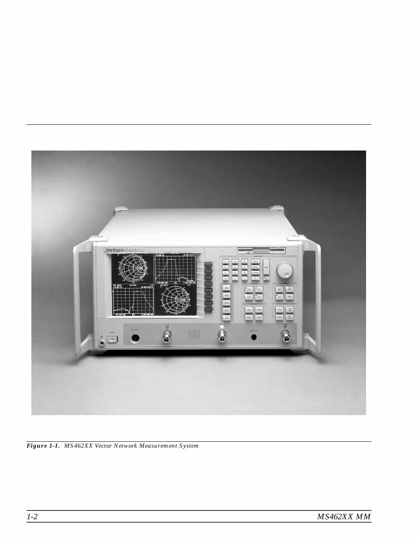
Figure 1-1. MS462XX Vector Network Measurement System
Chapter 1General Information
1-1 SCOPE OF THISMANUAL
This manual provides general information, performance verification, cali-bration, theory, and service information for the Anritsu MS462XX VectorNetwork Measurement System. The MS462XX Vector Network Measure-ment System is shown in Figure 1-1 (facing page).
1-2 INTRODUCTION This chapter provides information to familiarize the user with the basicMS462XX Vector Network Measurement System. Included is informationabout related manuals, and the available models and options.
1-3 RELATEDMANUALS
This manual is one of a five manual set consisting of this MaintenanceManual, the MS462XX Operation Manual (Anritsu part number10410-00203), the MS462XX Programming Manual (10410-00204), theMS462XX Scorpion Measurement Guide (10410-00213), and the MS462XXGPIB Quick Reference Guide (10410-00206).
1-4 MODELS With twelve basic models and a number of powerful options to choosefrom, the MS462XX can be configured to address many measurement re-quirements. The following models are available as platforms:
Model Number Frequency Range Configuration
MS4622A 10 MHz to 3 GHz Transmission/Reflection
MS4622B 10 MHz to 3 GHz Full Reversing
MS4622C 10 MHz to 3 GHz Direct Receiver Access
MS4622D 10 MHz to 3 GHz Balanced/Differential
MS4623A 10 MHz to 6 GHz Transmission/Reflection
MS4623B 10 MHz to 6 GHz Full Reversing
MS4623C 10 MHz to 6 GHz Direct Receiver Access
MS4623D 10 MHz to 6 GHz Balanced/Differential
MS4624A 10 MHz to 9 GHz Transmission/Reflection
MS4624B 10 MHz to 9 GHz Full Reversing
MS4624C 10 MHz to 9 GHz Direct Receiver Access
MS4624D 10 MHz to 9 GHz Balanced/Differential
The Transmission/Reflection models offer an economical solution for themanufacturing line that requires only S11 and S21 measurements withoutsacrificing the excellent performance of the Full Reversing models.
MS462XX MM 1-3
1-5 OPTIONS The following options are easily added to the MS462XX platform for in-creased measurement capabilities:
Option Number Description Availability
2 Time Domain All Models
3A Second Internal Source4 3 GHz Source – B Models
3B Second Internal Source4 6 GHz Source – B Models
3C Second Internal Source5 3 GHz Source – C Models
3D Second Internal Source5 6 GHz Source – C Models
3E Second Internal Source7 9 Ghz Source – D Models
3F Second Internal Source7 9 Ghz Source – C Models
4, 4D, 4F Noise Figure1 B, C and D Models Only
4B, 4E, 4G Noise Figure6 B, C and D Models Only
5 Frequency TranslatingGroup Delay
B and C Models Only
6 Third Test Port3 B and C Models Only
7 T/R Step Attenuator A Models Only
8 Harmonic Measurement All Models
10 AutoCal Control All Models
11 Test Port Connector All Models 2
13 Intermodulation Distortion All Models
24 Processing Upgrade B and C Models Only
1. 50 MHz to 3 GHz2. Standard Connector is N-female, No cost option for 3.5 mm (male), 3.5 mm (female),
N-Male, or GPC-7.3. Requires external source, 68XXX Synthesizer4. Third test port included5. Third output port included6. 50 MHz to 6 Ghz7. Third and Fourth output port included
1-6 IDENTIFICATIONNUMBER
The MS462XX Vector Network Measurement System’s ID number is af-fixed to the rear panel. Please use the complete ID number when orderingparts or corresponding with the Anritsu Customer Service department.
1-7 SERVICE POLICY The MS462XX Vector Network Measurement System’s modular design,extensive built-in diagnostics, and automated service tools are designedto support fast exchange of functional assembly level repairs.
Failed assemblies are not field repairable. Once an assembly is found tobe faulty, it should be returned to an authorized Anritsu Service Center(Table 1-4) for exchange.
1-4 MS462XX MM
OPTIONS GENERAL INFORMATION

1-8 SPARE PARTSLISTING
The assemblies and spare parts listed in Table 1-1 through Table 1-3 areavailable for the MS462XX Vector Network Measurement System. Refer toChapter 7 for removal and replacement procedures. Contact your nearestAnritsu Customer Service or Sales Center for price and availability informa-tion (Table 1-4).
GENERAL INFORMATION SPARE PARTS LISTING
MS462XX MM 1-5
Description Part Number
Main Source Module 52392
Optional Source Module 52393
CPU Board See Table 1-3
CPU Heatsink with Fan 650-34
CPU Boot PROM 58-1638
Lithium Battery (for CPU) 633-25
Receiver PCB See Table 1-3
Power Supply (PDU) Entire ND55521
Power Supply Fan Assembly ND49520
Power Supply Fuse 631-90
Option Module Assembly ND56500
Floppy Drive ND50711
LCD Display 15-100
LCD Backlight Driver PCB 2000-770
LCD Window (Plastic shield) 48177
Lamp for Sharp LQ9D340 LCD 632-55
Chassis (Instrument frame) D43325
Front Panel PCB, Keypad, Knob for 2 or 3 Ports ND48996
Front Panel PCB, Keypad, Knob for 4 Ports ND58272
Backplane PCB 48522-4
Test Port Connector (N Female) B45259
Test Port Connector (N Male) B45261
Test Port Connector (GPC-7) B47086
Test Port Connector (3.5mm Male) B47088
Test Port Connector (3.5mm F) B47087
Operating Software 2300-244
Boot Utility Software 2300-246
Handle, Standard (Right) D37169-4
Handle, Standard (Left) D37168-4
Table 1-1. Assemblies Common to All MS462XX Instruments
1-6 MS462XX MM
SPARE PARTS LISTING GENERAL INFORMATION
Description Part Number
AutoReverse Module (9 GHz units) 54530
AutoReverse Module (3 and 6 GHz units) 44666
Source Doubler Module (3 and 6 GHz units) 28875
Down Converter Module (3 and 6 GHz units) 29830
Down Converter Module (9 GHz units) 54610
Port 3 Module (all units) 44668
Port 1, 2 Module (all units) 46720
Tripler Module (9 GHz units) 56630
Hi Iso Switch (3 and 6 GHz units) 53077
Hi Iso Switch (9 GHz units) 60261
Non-Reversing Module (all units) 49983
Low Noise Amp for Opt. 4 (3 and 6 GHz units) 53300
Switch Module for Opt. 4 (3 and 6 GHz units) 46718
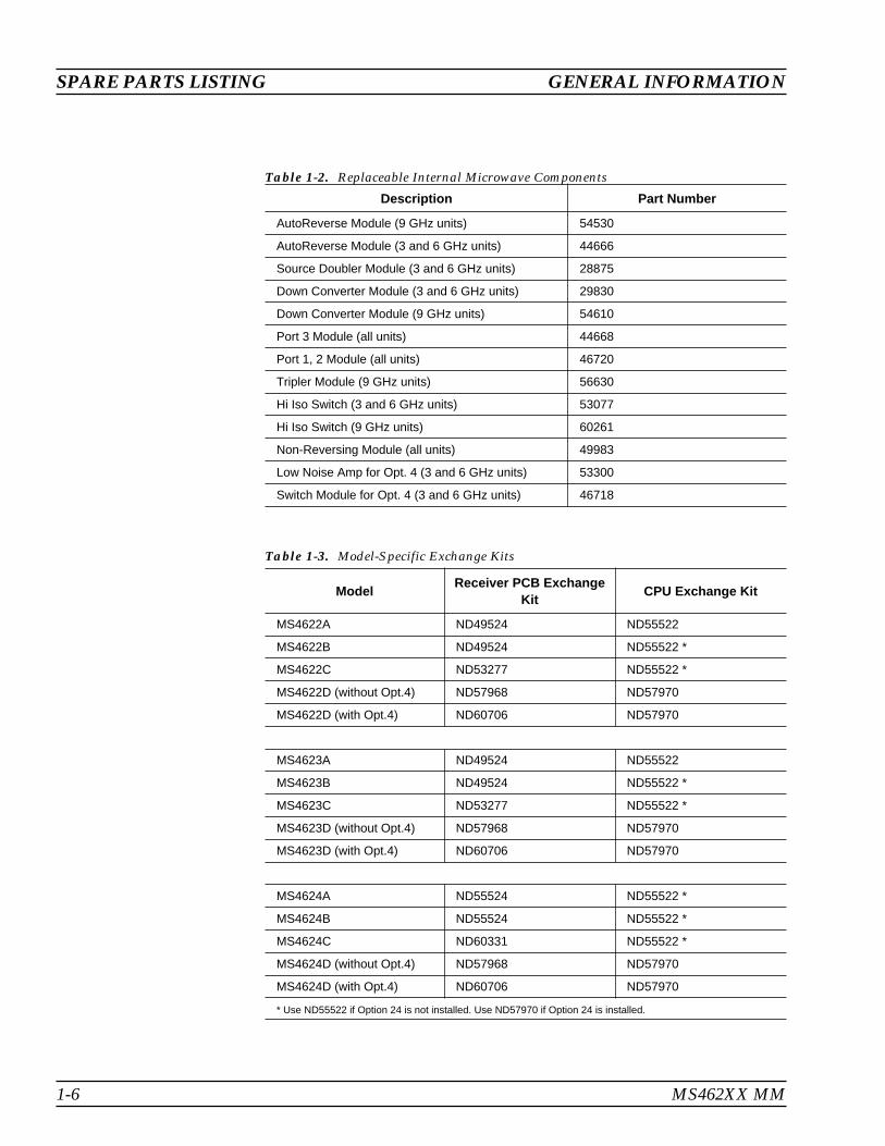
Table 1-2. Replaceable Internal Microwave Components
ModelReceiver PCB Exchange
KitCPU Exchange Kit
MS4622A ND49524 ND55522
MS4622B ND49524 ND55522 *
MS4622C ND53277 ND55522 *
MS4622D (without Opt.4) ND57968 ND57970
MS4622D (with Opt.4) ND60706 ND57970
MS4623A ND49524 ND55522
MS4623B ND49524 ND55522 *
MS4623C ND53277 ND55522 *
MS4623D (without Opt.4) ND57968 ND57970
MS4623D (with Opt.4) ND60706 ND57970
MS4624A ND55524 ND55522 *
MS4624B ND55524 ND55522 *
MS4624C ND60331 ND55522 *
MS4624D (without Opt.4) ND57968 ND57970
MS4624D (with Opt.4) ND60706 ND57970
* Use ND55522 if Option 24 is not installed. Use ND57970 if Option 24 is installed.
Table 1-3. Model-Specific Exchange Kits

1-9 ASSEMBLYEXCHANGEPROGRAM
Anritsu maintains an exchange assembly program for selected MS462XXsubassemblies and RF components. If a malfunction occurs in one of thesesubassemblies, the defective unit can be exchanged. All exchange subassem-blies or RF components are warrantied for 90 days from the date of shipment,or the balance of the original equipment warranty, whichever is longer. Ahard copy or saved to disk copy of the instrument Service Log must accom-pany all exchange modules. To access the Service Log, press the Utility frontpanel key, followed by the SERVICE LOG menu soft key. Select either PRINTLOG or SAVE LOG TO DISK.
NOTEWhen sending an assembly to the factory for exchange, acopy of the Service Log must accompany the assembly. Ex-change prices can only be offered if the Service Log data isincluded with the assembly to be exchanged.
Please have the exact model number and serial number of your unit availablewhen requesting this service, as the information about your system is filedaccording to the instrument model and serial number. For more informationabout the assembly exchange program, contact your local sales representativeor call your local Anritsu Service Center. Refer to Table 1-4 for a list of cur-rent Anritsu Service Centers.
1-10 PREVENTIVEMAINTENANCE
The MS462XX CPU module contains a battery-backed memory/real timeclock chip (BBRAM) and a static memory (SRAM) backup battery. TheBBRAM chip has a rated life span of 10 years, and the SRAM backup batteryhas a worst-case life span of two years at 25°C when the instrument is stored(always off). Exposure to temperatures above 60°C will dramtically reducethis worst-case life span. The SRAM backup battery should be replaced everythree years.
For instruments with serial number 995299 and below, the LCD (Anritsu partnumber 15-92) contains a backlight flourescent lamp that has a rated 10,000hour life span. For instruments with serial number 000101 and above, theLCD (Anritsu part number 15-100) contains a backlight flourescent lamp thathas a rated 50,000 hour life span. Both the SRAM backup battery andbacklight lamp should be replaced periodically per the procedures in Chap-ter 7.
1-11 RECOMMENDEDTESTEQUIPMENT
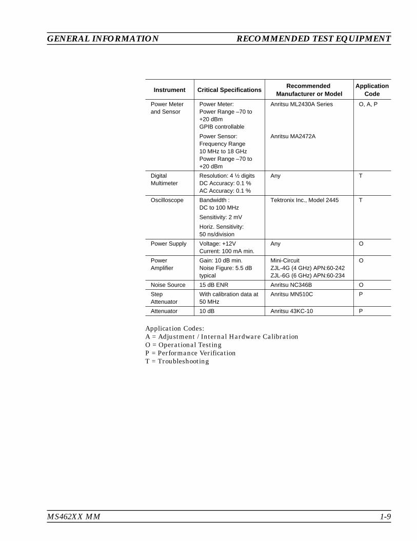
The following test equipment is recommended for servicing the MS462XXVector Network Measurement System. The list is a suggestion and by nomeans comprises a comprehensive list of all equipment necessary to servicethis system. Functionally equivalent equipment may be substituted for therecommended manufacturer or model as long as the critical specifications aremet. Inclusion on this list does not constitute an endorsement or suitability ofpurpose of any particular equipment or manufacturer. The Application Codecolumn of the following table represents when or where the specified equip-ment would be used:
GENERAL INFORMATION ASSEMBLY EXCHANGE PROGRAM
MS462XX MM 1-7

Instrument Critical SpecificationsRecommended
Manufacturer or ModelApplication
Code
Computer orController
Personal Computer:Pentium class proces-sor, Win 95(16 MB RAM min.)
GPIB Interface
Any Desktop PC:
National InstrumentsPCI-GPIB or AT-GPIB/TNT(plug-and-play)
Notebook PC:National InstrumentsPCMCIA-GPIB
O, P
PerformanceVerificationSoftware
Anritsu 2300-482 P
GPIB Cable Anritsu 2100-X O, P, A
RF/MicrowaveCable
DC to 6 GHz, K or 3.5mm connectors (maleor female)
Any O
Printer PortTest
Anritsu ND51900 O
Throughline (3 each) Anritsu 3670A50-2,3670K50-2, 3670N50-2,3670NN50-2
O, P
Calibration Kit
N test port connector Anritsu 3753LF/3753R withOption 1 and 3
O, P
3.5 mm test portconnector
Anritsu 3750LF/3750R withOption 1 and 3
O, P
GPC-7 test portconnector
Anritsu 3751LF/3751R withOption 3
O, P
Short Two each of:N male test portN female test port3.5mm male test port3.5mm female test portGPC-7 test port
Anritsu 23NF50Anritsu 23N50Anritsu 23LF50Anritsu 23L50Anritsu 23A50
O
Verification Kit N test port connector3.5mm test port con-nectorGPC-7 test port con-nector
Anritsu 3663LF/3663RAnritsu 3666LF/3666R
Anritsu 3667LF/3667R
P
FrequencyCounter
Frequency: 1 to 20 GHzInput Impedance: 50 �
Frequency Stability:Temperature = 1x10⁻⁷
Anritsu MF2412B orEIP Microwave, Inc.,Model 548B
A
1-8 MS462XX MM
RECOMMENDED TEST EQUIPMENT GENERAL INFORMATION
Instrument Critical SpecificationsRecommended
Manufacturer or ModelApplication
Code
Power Meterand Sensor
Power Meter:Power Range –70 to+20 dBmGPIB controllable
Power Sensor:Frequency Range10 MHz to 18 GHzPower Range –70 to+20 dBm
Anritsu ML2430A Series
Anritsu MA2472A
O, A, P
DigitalMultimeter
Resolution: 4 ½ digitsDC Accuracy: 0.1 %AC Accuracy: 0.1 %
Any T
Oscilloscope Bandwidth :DC to 100 MHz
Sensitivity: 2 mV
Horiz. Sensitivity:50 ns/division
Tektronix Inc., Model 2445 T
Power Supply Voltage: +12VCurrent: 100 mA min.
Any O
PowerAmplifier
Gain: 10 dB min.Noise Figure: 5.5 dBtypical
Mini-CircuitZJL-4G (4 GHz) APN:60-242ZJL-6G (6 GHz) APN:60-234
O
Noise Source 15 dB ENR Anritsu NC346B O
StepAttenuator
With calibration data at50 MHz
Anritsu MN510C P
Attenuator 10 dB Anritsu 43KC-10 P
Application Codes:A = Adjustment / Internal Hardware CalibrationO = Operational TestingP = Performance VerificationT = Troubleshooting
GENERAL INFORMATION RECOMMENDED TEST EQUIPMENT
MS462XX MM 1-9

1-12 CONVENTIONS Throughout this manual, path names may be used to represent the key-strokes for a desired action or procedure. The path name begins with a frontpanel key selection, followed by additional front panel or soft key selections,each separated by a forward slash (/). Front panel key names and soft keysare presented in the manual as they are on the system, that is, in initial capsor all uppercase letters as appropriate. For example, the following path namerepresentation displays the system model number, serial number, currentsoftware version, and installed options:
Utility/INSTRUMENT STATE PARAMETERS/SYSTEM
Following the path above, the user would press the Utility front panel key, fol-lowed by the INSTRUMENT STATE PARAMETERS soft key, then the SYSTEMsoft key to display the system information.
Individual steps within a procedure may also be presented as sequentiallynumbered steps for clarity. Again, front panel key names and soft keys arepresented in the manual as they are on the system. For example, the follow-ing procedure displays the system model number, serial number, current soft-ware version, and installed options:
1. Press the Utility front panel key.
2. Select the menu soft keys as follows:
INSTRUMENT STATE PARAMETERS
SYSTEM
1-10 MS462XX MM
CONVENTIONS GENERAL INFORMATION

1-13 COMPONENTHANDLING
The MS462XX series contains components that can be damaged by staticelectricity. The following figures illustrate the precautions that should befollowed when handling static-sensitive subassemblies and components.If followed, these precautions will minimize the possibilities of static-shock damage to these items.
NOTEUse of a grounded wrist strap when removing and/or re-placing subassemblies or parts is strongly recommended.
1. Do not touch exposed contacts on anystatic sensitive component.
2. Do not slide static sensitive compo-nent across any surface.
3. Do not handle static sensitive compo-nents in areas where the floor or worksurface covering is capable of generat-ing a static charge.
4. Wear a static-discharge wristbandwhen working with static sensitivecomponents.
5. Label all static sensitive devices. 6. Keep component leads shorted to-gether whenever possible.
GENERAL INFORMATION COMPONENT HANDLING
MS462XX MM 1-11
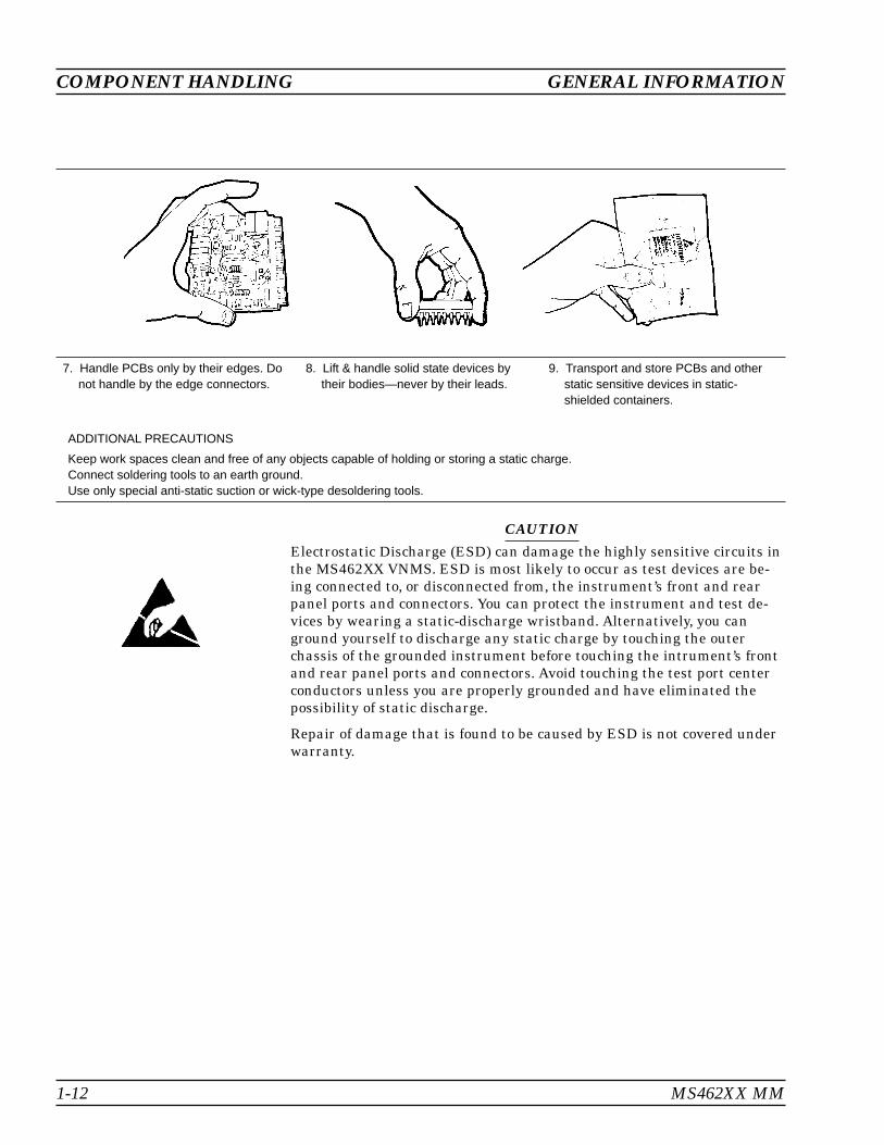
7. Handle PCBs only by their edges. Donot handle by the edge connectors.
8. Lift & handle solid state devices bytheir bodies—never by their leads.
9. Transport and store PCBs and otherstatic sensitive devices in static-shielded containers.
ADDITIONAL PRECAUTIONS
Keep work spaces clean and free of any objects capable of holding or storing a static charge.Connect soldering tools to an earth ground.Use only special anti-static suction or wick-type desoldering tools.
CAUTION
Electrostatic Discharge (ESD) can damage the highly sensitive circuits inthe MS462XX VNMS. ESD is most likely to occur as test devices are be-ing connected to, or disconnected from, the instrument’s front and rearpanel ports and connectors. You can protect the instrument and test de-vices by wearing a static-discharge wristband. Alternatively, you canground yourself to discharge any static charge by touching the outerchassis of the grounded instrument before touching the intrument’s frontand rear panel ports and connectors. Avoid touching the test port centerconductors unless you are properly grounded and have eliminated thepossibility of static discharge.
Repair of damage that is found to be caused by ESD is not covered underwarranty.
1-12 MS462XX MM
COMPONENT HANDLING GENERAL INFORMATION

1-14 SERVICECENTERS
GENERAL INFORMATION SERVICE CENTERS
MS462XX MM 1-13/1-14
UNITED STATESANRITSU COMPANY490 Jarvis DriveMorgan Hill, CA 95037-2809Telephone: (408) 776-83001-800-ANRITSUFAX: 408-776-1744
FRANCEANRITSU S.A9 Avenue du QuebecZone de Courtaboeuf91951 Les Ulis CedexTelephone: 016-09-21-550FAX: 016-44-61-065
JAPANANRITSU CUSTOMER SERVICES LTD.1800 Onna Atsugi-shiKanagawa-Prf. 243 JapanTelephone: 0462-96-6688FAX: 0462-25-8379
ANRITSU COMPANY10 New Maple Ave., Unit 305Pine Brook, NJ 07058Telephone: (973) 227-89991-800-ANRITSUFAX: 973-575-0092
GERMANYANRITSU GmbHGrafenberger Allee 54-56D-40237 Dusseldorf, GermanyTelephone: 0211-968550FAX: 0211-9685555
SINGAPOREANRITSU (SINGAPORE) PTE LTD.10, Hoe Chiang Road#07-01/02 Keppel TowersSingapore 089315Telephone: 6-282-2400FAX: 6-282-2533
ANRITSU COMPANY1155 E. Collins BlvdRichardson, TX 75081Telephone: 1-800-ANRITSUFAX: 972-671-1877
INDIAMEERA AGENCIES PVT. LTD.23 Community CentreZamroodpur, Kailash Colony Extension,New Delhi, India 110 048Phone: 011-2-6442700/6442800FAX : 011-2-644250023
SOUTH AFRICAETECSA12 Surrey Square Office Park330 Surrey AvenueFerndale, Randburt, 2194South AfricaTelephone: 011-27-11-787-7200FAX: 011-27-11-787-0446
AUSTRALIAANRITSU PTY. LTD.Unit 3, 170 Foster RoadMt Waverley, VIC 3149AustraliaTelephone: 03-9558-8177FAX: 03-9558-8255
ISRAELTECH-CENT, LTD.4 Raul Valenberg StTel-Aviv 69719Telephone: (03) 64-78-563FAX: (03) 64-78-334
SWEDENANRITSU ABBorgafjordsgatan 13164 40 KISTA, SwedenTelephone: +46-8-53470700FAX: +46-8-53470730
BRAZILANRITSU ELECTRONICA LTDA.Praia de Botafogo, 440, Sala 2401CEP22250-040, Rio de Janeiro, RJ, BrasilTelephone: 021-527-6922FAX: 021-53-71-456
ITALYANRITSU Sp.ARoma OfficeVia E. Vittorini, 12900144 Roma EURTelephone: (06) 50-99-711FAX: (06) 50-22-425
TAIWANANRITSU CO., INC.7F, No. 316, Section 1NeiHu RoadTaipei, Taiwan, R.O.C.Telephone: 886-2-8751-1816FAX: 886-2-8751-2126
CANADAANRITSU INSTRUMENTS LTD.700 Silver Seven Road, Suite 120Kanata, Ontario K2V 1C3Telephone: (613) 591-2003FAX: (613) 591-1006
KOREAANRITSU CORPORATION LTD.8F Hyunjuk Building, 832-41Yeoksam Dong, Kangnam-KuSeoul, South Korea 135-080Telephone: 02-553-6603FAX: 02-553-6605
UNITED KINGDOMANRITSU LTD.200 Capability GreenLuton, BedfordshireLU1 3LU, EnglandTelephone: 015-82-433200FAX: 015-82-731303
CHINAANRITSU ELECTRONICS (SHANGHAI) CO. LTD.2F, Rm B, 52 Section Factory BuildingNo. 516 Fu Te Rd (N)Shanghai 200131 P.R. ChinaTelephone:21-58680226, 58680227, 58680228FAX: 21-58680588
Table 1-4. Anritsu Service Centers


Table of Contents
2-1 INTRODUCTION . . . . . . . . . . . . . . . . . . . . . . . . . . . . . . . . . . . 2-3
2-2 SYSTEM OVERVIEW . . . . . . . . . . . . . . . . . . . . . . . . . . . . . . . . . 2-3
2-3 SOURCE MODULE . . . . . . . . . . . . . . . . . . . . . . . . . . . . . . . . . . 2-4Digital Interface . . . . . . . . . . . . . . . . . . . . . . . . . . . . . . . . . . 2-5Main Oscillator Loops . . . . . . . . . . . . . . . . . . . . . . . . . . . . . . . 2-5Offset Oscillator Loops . . . . . . . . . . . . . . . . . . . . . . . . . . . . . . 2-5DDS Reference Clock . . . . . . . . . . . . . . . . . . . . . . . . . . . . . . . 2-6Bounding Circuitry . . . . . . . . . . . . . . . . . . . . . . . . . . . . . . . . 2-6Speed-Up Circuitry . . . . . . . . . . . . . . . . . . . . . . . . . . . . . . . . 2-7Frequency Bands and Switched Filters. . . . . . . . . . . . . . . . . . . . . . 2-7Heterodyne Oscillator . . . . . . . . . . . . . . . . . . . . . . . . . . . . . . . 2-7ALC Circuitry . . . . . . . . . . . . . . . . . . . . . . . . . . . . . . . . . . . 2-8Operation Modes. . . . . . . . . . . . . . . . . . . . . . . . . . . . . . . . . . 2-8
2-4 RECEIVER MODULE . . . . . . . . . . . . . . . . . . . . . . . . . . . . . . . . 2-10Down Conversion Module . . . . . . . . . . . . . . . . . . . . . . . . . . . . 2-10Digital Interface . . . . . . . . . . . . . . . . . . . . . . . . . . . . . . . . . 2-10Test Channel Intermediate Frequency Path . . . . . . . . . . . . . . . . . . 2-11Reference Channel Intermediate Frequency Path . . . . . . . . . . . . . . . 2-12Sampling of the Intermediate Frequency . . . . . . . . . . . . . . . . . . . . 2-13ADC Clock Generation/ DSP Communication Port Interface . . . . . . . . . 2-1410 MHz Clock Distribution . . . . . . . . . . . . . . . . . . . . . . . . . . . 2-14RF Component Control. . . . . . . . . . . . . . . . . . . . . . . . . . . . . . 2-14
Chapter 2Theory of Operation

2-5 FRONT END RF COMPONENTS . . . . . . . . . . . . . . . . . . . . . . . . . . 2-15Test Port Connectors . . . . . . . . . . . . . . . . . . . . . . . . . . . . . . . 2-15Switched Frequency Doubler Module . . . . . . . . . . . . . . . . . . . . . . 2-15Switched Frequency Tripler Module . . . . . . . . . . . . . . . . . . . . . . 2-15Auto-Reversing Module . . . . . . . . . . . . . . . . . . . . . . . . . . . . . 2-15Non-Reversing Module . . . . . . . . . . . . . . . . . . . . . . . . . . . . . . 2-16Step Attenuator . . . . . . . . . . . . . . . . . . . . . . . . . . . . . . . . . 2-16Port Module. . . . . . . . . . . . . . . . . . . . . . . . . . . . . . . . . . . . 2-16Port 3 Module. . . . . . . . . . . . . . . . . . . . . . . . . . . . . . . . . . . 2-16Low Noise Pre-Amplifier . . . . . . . . . . . . . . . . . . . . . . . . . . . . . 2-16Switched Module . . . . . . . . . . . . . . . . . . . . . . . . . . . . . . . . . 2-16High Isolation Switch Module . . . . . . . . . . . . . . . . . . . . . . . . . . 2-16Receiver Module Configurations. . . . . . . . . . . . . . . . . . . . . . . . . 2-16Receiver Module Configurations, MS462XA . . . . . . . . . . . . . . . . . . 2-17Receiver Module Configurations, MS462XB . . . . . . . . . . . . . . . . . . 2-17Receiver Module Configurations, MS462XC . . . . . . . . . . . . . . . . . . 2-18Receiver Module Configurations, MS462XD . . . . . . . . . . . . . . . . . . 2-19Option 3—Second Source . . . . . . . . . . . . . . . . . . . . . . . . . . . . 2-20Option 4—Noise Figure Measurement Capability . . . . . . . . . . . . . . . 2-20Option 6—Third Test Port . . . . . . . . . . . . . . . . . . . . . . . . . . . . 2-21
2-6 OPTION MODULES . . . . . . . . . . . . . . . . . . . . . . . . . . . . . . . . . 2-21General . . . . . . . . . . . . . . . . . . . . . . . . . . . . . . . . . . . . . . 2-21Frequency Translating Group Delay (FTGD) Synthesizer . . . . . . . . . . . 2-22Frequency Translating Group Delay Receiver . . . . . . . . . . . . . . . . . 2-23Wideband Noise Figure Receiver . . . . . . . . . . . . . . . . . . . . . . . . 2-23
2-7 CENTRAL PROCESSOR MODULE. . . . . . . . . . . . . . . . . . . . . . . . . 2-25
2-8 RECEIVER MODULE BLOCK DIAGRAMS . . . . . . . . . . . . . . . . . . . . 2-25
2-2 MS462XX MM
Table of Contents (Continued)

Chapter 2Theory of Operation
2-1 INTRODUCTION This chapter provides a brief overview of the functional assemblies andmajor parts that comprise a typical MS462XX Vector Network Measure-ment System. It also briefly describes the operation of each major assem-bly.
2-2 SYSTEMOVERVIEW
MS462XA/B Series Vector Network Measurement Systems are ratio mea-surement systems used to measure complex vector signal characteristicsof devices and systems in the 10 MHz to 9 GHz range. They also incorpo-rate special measurement capabilities such as Noise Figure measure-ment, Intermodulated Distortion measurement, and more.
The MS462XC Series Vector Network Measurement Systems are config-ured as Direct Access Receivers for antenna, frequency conversion, andmultiple output device measurements in the 10 MHz to 9 GHz range.They also maintain the ability to measure all four S-parameters with theaddition of a reflectometer setup at the front end of the receiver.
The MS462XD Series Vector Network Measurement Systems are used tomeasure complex vector signal characteristics of multiport balanced/dif-ferential devices and systems in the 10 MHz to 9 GHz range.
The MS462XX performs complex vector signal measurements by sourcinga stimulus signal to the Device Under Test (DUT) connected to the frontpanel Port 1, Port 2, Port 3 (optional for MS462XB), or Port 4 (forMS462XD) connectors. It simultaneously measures the DUT response,which consists of reflected or transmitted (attenuated or amplified) sig-nals at the connectors of the DUT. The reflected or transmitted signal(s)and a sample of the stimulus signal are down converted to 125 kHz inter-mediate frequency (IF) signals.
These IF signals are then converted into digital information and sent tothe Central Processor Module where the digital information is processedby a Digital Signal Processor (DSP) using Single Frequency Digital Fou-rier Transfer to determine the magnitude and phase of the signal beingmeasured. The information is then normalized for the desired S-parame-ter and presented to the user via the front panel color LCD display. Thedisplay information is also available on the rear panel VGA Out connec-tor for use with an external VGA monitor.
The normalized measurement information is also available on the rearpanel Printer Out connector and Dedicated GPIB connector for use withan external printer and plotter respectively.
MS462XX MM 2-3

A front panel keypad, rotary knob, and IBM compatible keyboard inter-face provide user interaction with the MS462XX Central Processor Mod-ule. The system is also equipped with a floppy disk drive and non-volatileinternal memory for storage and retrieval of data and front panel setupinformation.
The MS462XX implements an IEEE 488.2 GPIB interface that allows anexternally connected instrument controller to control the MS462XX sys-tem in the “Remote-Only” mode. All MS462XX measurement and in-put/output operations may be controlled remotely in this mode.
An internal service log stores a record of system failures, data about thefailures, and other key system service information. The service log is im-plemented using an internal battery-backed SRAM memory.
2-3 SOURCE MODULE There are two source modules for the MS462XX Series Vector NetworkMeasurement System. The Source/Local Oscillator Module is standard onall models and an Optional Source Module is installed when using 3- and4-port configurations with an active internal source.
The Source/Local Oscillator module generates the primary source RF andlocal oscillator output. This module contains the phase lock circuitry forthe oscillator’s circuitry to generate different output frequency bands cov-ering 10 MHz to 3000 MHz, and banks of switched filter sections. Thesource output level is controllable through an ALC loop, whereas the Lo-cal Oscillator output level is fixed. In addition to the Source and Local Os-cillator RF outputs, this module also provides Common Offset and Het-erodyne VCO signals used by the optional second source.
The optional Source module generates the optional source RF output.This module contains the phase lock circuitry for the oscillator’s circuitryto generate different output frequency bands spanning 10 MHz to3000 MHz, and banks of switched filter sections. The source output levelis controllable through an ALC loop. The module receives the CommonOffset and Heterodyne VCO signals from the Primary Source/Local Oscil-lator Number modules.
While both modules are similar, the Source/ Local Oscillator module is afully laden assembly, while the optional Source module contains only thecircuitry for the optional source output. Each module has a separate PCBassembly, but both use a common housing.
Typical RF output specifications for the modules are:
RF Output Frequency Range: 10 MHz to 3 GHz
Unleveled Source Port Power Level: 27 dBm Max., 16 dBm Min.
LO Port Power Level: 12 dBm Max., 1 dBm Min.
RF Output Frequency Range: 800 MHz to 1600 MHz
Heterodyne Output Power Level: 4 dBm Max., –3 dBm Min.
Common Offset Power Level: 7 dBm Max., 1 dBm Min.
2-4 MS462XX MM
SOURCE MODULE THEORY OF OPERATION

The internal ALC level loop allows for a leveled range of –11 dBm to+20 dBm out of the Source RF port.
The Local Oscillator is not used on the optional Source module. All fre-quency loops are phase locked to the internal 10 MHz reference oscillatorin the MS462XX.
NOTESix gigahertz instruments use a Switched Doubler moduleimmediately following the source(s). Nine gigahertz instru-ments use a Switched Tripler module immediately followingthe source(s). The doublers or triplers are installed on theReceiver PCB assembly.
Digital Interface All modules in the instrument share the same bus connections to the mi-croprocessor via the motherboard. The common data and address bus con-sists of 16 data bits, 5 address lines, and 5 board select lines. Within theSource/LO module, the incoming address and board select lines are de-coded to direct data between the common bus and internal modulelatches. Transceivers are used to buffer the common data bus from an in-ternal data bus. When a latch located on the module is addressed, thetransceivers will enable the transfer of data to or from the internal databus.
Main OscillatorLoops
The Source and LO RF outputs are both generated by voltage controlledoscillators (VCOs) that nominally cover 800 to 1600 MHz. The outputs ofthe VCOs are processed to ultimately produce the final outputs of themodule. Additionally, the outputs of the main oscillators are sampled andfed back, in order to be phase-locked to the system reference 10 MHz. Thephase locking circuitry for the Source and LO VCOs are essentially iden-tical in their implementation.
When phase locking the main oscillator, the VCO is mixed with an offsetoscillator to produce a lower frequency signal. This mixed down signal isinput to a phase detector and is compared to a signal produced by a Di-rect Digital Synthesis (DDS) IC. The DDS has better than 1 Hz resolu-tion, which is transferred to the main VCO. The phase detector output isfed into a loop filter, which supplies the tuning voltage (0.5 to 20 volts) tothe VCO.
Offset OscillatorLoops
The offset oscillator used by the source and the LO are also 800 to1600 MHz VCOs. The VCOs are also phase-locked to the system’s 10 MHzreference (fref) using a PLL IC. The PLL IC integrates two programmabledividers, a prescaler and a phase/frequency detector. The PLL IC operatesin frequency ranges up to 2.5 GHz. The circuitry used to lock up thesource offset oscillator is reproduced for the LO offset VCO.
The outputs of the two dividers are programmed to 625 kHz. The phasedetector issues a correction current pulse using the internal charge pump.The loop amplifier integrates current pulses from the PLL IC. The tuningsensitivity at the VCO input is approximately 50 MHz/V.
THEORY OF OPERATION SOURCE MODULE
MS462XX MM 2-5

The loop amplifier has a gain of 4; therefore, the sensitivity at the PLL ICoutput is very high. Thus, any noise injected at this point has noticeableaffects on the output noise characteristics.
DDS ReferenceClock
In order to generate accurate DDS frequencies, an accurate referenceclock must be provided to the two DDS ICs. The 32 bits of the DDS fre-quency register allow the minimum output resolution of Fclk divided by232. By phase locking the DDS reference clock VCXO to 26.8435456 MHz,the resulting minimum resolution is 0.00625 Hz.
To get such a precision frequency from the VCXO, it is phase-locked to thesystem’s 10 MHz reference. A third DDS IC, using the VCXO as its clock,is programmed to output 100 kHz. The system reference is divided downto 100 kHz and is compared against the DDS output. Only when the clockis exactly 26.8435456 MHz will the programmed DDS produce a phaselocked 100 kHz.
The phase detector feeds back to the VCXO tuning line to precisely tunethe clock frequency.
Bounding Circuitry Bounding is a term for the circuitry that is used to ensure that the VCOsare kept within their range and that the correct frequency is generated.
The mixing of the main and offset signals produces an additive as well asthe desired subtractive product. Therefore, there is the potential that themain oscillator loops will try to lock on to the wrong signal. To preventlocking on the wrong side, additional PLL ICs are wrapped around themain loop phase detector as bounding circuits. The proper polarity in theloop requires that the main oscillator always be lower in frequency thanthe offset oscillator.
The upper bound PLL is programmed for the offset VCO frequency. Whenthe main VCO goes higher in frequency than the offset VCO, a correctionpulse is generated that is fed into the main oscillator loop. This magni-tude of the correction pulse is large enough to push the main VCO to thecorrect side.
In addition to being prevented from swinging too high, the main VCOmust also be bounded on the low end. For lower main VCO frequencies,the difference frequency increases. However, the mixer has a limitedbandwidth. When the bandwidth is exceeded, the output response dropsoff and it will seem as if the main VCO is too high in frequency, instead oftoo low. Once again, positive feedback would result. A lower bound PLLwill issue a correction pulse to push the main VCO higher in frequencywhen the bound is exceeded.
Both the source and the LO sides incorporate bounding circuits. When themain VCO is within an acceptable range, there is no contribution fromthe bounding circuits. The PLL ICs used for the bounding circuits are thesame components used in the offset VCO loops.
2-6 MS462XX MM
SOURCE MODULE THEORY OF OPERATION

Speed-Up Circuitry In addition to the phase-lock and bounding circuitry, there is also cir-cuitry to help speed the locking of the loop. The settling time of the mainloop and its phase detector is very slow. Frequency lock detect circuitryemits pulses to help get the source main VCO locked on frequencyquicker. Once on frequency, the speed-up circuit’s contribution drops outand the normal phase lock circuitry locks up the loop the rest of the way.In this way, the loop locking occurs more rapidly, but the stability of theloop is not compromised.
However, for this speedup to work, the polarity of the loop must be cor-rect. If on the wrong side, then the speedup circuitry only acts to push theVCO even farther off, even faster. Thus a hierarchy of control must be es-tablished. The bounding correction circuits must be strong enough tocounter the contribution of the speedup circuits, but should not be sostrong that the loop ends up banging back and forth between its two ex-tremes.
Frequency Bandsand Switched
Filters
Although the main oscillator produces an output of 800 to 1600 MHz only,the module output frequency covers 10 MHz to 3 GHz. There are four dis-tinct bands of operation to achieve the desired frequency range. If the de-sired output frequency is between 10 to 400 MHz, the circuit is in the het-erodyne mode. The VCO output is mixed with a heterodyne oscillator(typically 1200 MHz). Passing the VCO output through a divide-by-twocircuit produces frequencies between 400 to 800 MHz. For 800 to1600 MHz, the VCO signal passes directly. To achieve 1600 to 3000 MHz,a doubler is used.
To improve harmonics and spurious performance, output signals arepassed through switched filter sections. A given frequency mode (Hetero-dyne, divide-by-two, through, or multiply-by-two) may have one or moreswitched filter band sections. The switching for the frequency generationmodes is combined with the control for the switched filter section.
HeterodyneOscillator
In the heterodyne mode, a heterodyne oscillator is used to mix with themain VCO outputs of the source and LO to generate frequencies less than400 MHz. This VCO is the same type as that used for the main and offsetloops. The VCO has an 800 to 1600 MHz range, but will typically be tunedto 1200 MHz. The main VCO is tuned higher than the fixed heterodyneoscillator, so that positive steps in system frequency will correspond topositive steps in the main VCO. To avoid mixing spurs, the heterodyneVCO is allowed to step down as far as 900 MHz. The circuitry for thephase-locking of this heterodyne oscillator is similar to the offset VCOlocking. The heterodyne VCO signal is also passed along out of the mod-ule to be supplied to the optional source for use in its heterodyne mode.
THEORY OF OPERATION SOURCE MODULE
MS462XX MM 2-7

ALC Circuitry The source side differs from the LO side primarily in its ability to havecontrollable output power. The feedback from a level detector controls thelevel of the source output. The level of the signal can be controlled over a20 dB range. In the ALC circuitry, a DAC is set to a calibrated value for adesired power level. The ALC loop then adjusts the level of the sourceoutput until the detector output matches the reference voltage. A shapercircuit compensates for the non-linear characteristics of the modulatorand doubler.
Once placed into a system, the Source/LO Module may be calibrated forleveled power out of the port. In general, the Power Level DAC is steppedwhile the Source is tuned to a fixed frequency. The port output level ismeasured with a power meter. The power level at the port is dependentnot only on the source output power itself, but also upon the lossesthrough various components in the RF deck. The results are then used tocurve-fit an equation that relates DAC values to port power. For a 3 GHzsystem, the measurements are performed at 1 GHz. If the system is a6 GHz unit, the measurements are performed at both 1 GHz and 4 GHz.
The power curve did not change much with frequency, only the offsets.Therefore, the same curve-fit equations could be used with a correctionfor the different offsets at various frequencies. The curve-fit equation cal-culated using 1 GHz data is applied for system frequencies less than3 GHz. The 4 GHz curve-fit equation is used in the doubler band (i.e. fre-quencies greater than 3 GHz). The power DAC is set to a 0 dBm portpower using the appropriate curve-fit equation, then the resulting erroroffset is measured. The offsets for different frequency steps are stored ina table and intermediary frequencies are interpolated.
Additionally, a shaper DAC calibration is performed when the system is a6 GHz unit. The shaper DAC is in place to help compensate for changes inthe doubler characteristics.
At band switch points, the source takes longer to settle. During the set-tling period, there is a lack of RF signal to the ALC detector diode, thusthe ALC circuitry will set the output power higher. Therefore, the ALC islevel-dipped at band switch points to prevent large power spikes from hit-ting the DUT during these transition periods. The level-dip is performedby switching a fixed voltage into the loop.
Operation Modes There are two operation modes:
CommonOffset Mode
Traditionally, the source and LO output signals are generatedindependently. An alternative mode of operation is possiblewhere the LO offset VCO also locks up the source loop. Thesource offset VCO is disabled in this mode. The DDS outputs onthe two sections then make up the frequency difference betweenthe two outputs. Sharing a common offset VCO allows the twosignal sources to better track each other. The resulting IF hasbetter phase noise because much of the offset VCO noise isratioed out.
2-8 MS462XX MM
SOURCE MODULE THEORY OF OPERATION
To make accurate measurements, the IF must be settled beforethe Digital Signal Processing (DSP) is triggered. When operat-ing in common offset mode, the IF settles faster. In fact, eventhough the offset VCO (and therefore the main VCOs) may stillbe slewing in phase, the IF itself may already be settled becausethe Source and LO are tracking. The two main VCOs are able totrack the offset VCO settling because of their higherbandwidths. Therefore, measurements can be made sooner inthe common offset mode and overall system speed is thus faster.
However, the common offset mode can only be used when thesource and LO frequencies are relatively close, because therange of the DDS limits the allowable difference. Additionally,the source and LO must be operating in the same frequencyband. High-IF frequency measurements, such as Wide-BandNoise Figure, must operate in the independent offset mode.However, common offset mode is beneficial for typical S-parame-ter measurements where speed is an important parameter.
HarmonicGeneratorMode
In most measurements, the presence of harmonics on the RF isundesirable. However, for measurements of phase in the har-monic measurements application, a reference is needed. The sec-ond and third harmonics of the source are used, and thereforemust be of a significant enough level to be measured accurately.A harmonic generator diode can be switched into the circuit topump the harmonics to levels above –45 dBc. Without the har-monic generator, the harmonics may be lower than –45 dBc.
THEORY OF OPERATION SOURCE MODULE
MS462XX MM 2-9

2-4 RECEIVER MODULE The Receiver module is made up of the RF components that are used toconfigure the system for the various options. This encompases the fre-quency translation module, which produces the 125 kHz IntermediateFrequency, the Test and Reference channel Intermediate Frequencypaths, the system 10 MHz time base, and the circuitry for the control ofthe RF components. At the end of the Intermediate Frequency paths, thesignal to be measured is sampled and sent to the Central Processor Mod-ule. This module has Digital Signal Processing (DSP) prior to processingthe numerical values into the CPU. Determination of magnitude andphase for S-Parameter measurements is done by calculating a single fre-quency Digital Fourier Transfer (DFT) of a coherently sampled Interme-diate Frequency Signal. A Programmable Logic Device (PLD) accom-plishes control of the receiver board and Analogue to Digital (ADC) clockgeneration.
An intermediate frequency signal of 125 kHz was chosen because of thedivision ratio to the 10 MHz reference combined with the optimized sam-ple rates used in the analogue to digital conversions.
Down ConversionModule
The Down Conversion Module (DCM) translates the Test Port and theReference Port signals down to the 125 kHz intermediate frequency sig-nal.
The input at J5 takes the local oscillator signal from the Source Module.The signal is split into two paths, one for the Test Port Mixer and theother for the Reference Port Mixer. Two identical paths are used to pro-vide the mixer local oscillator drive. The reason for the two paths is tomaintain good isolation between the two signal paths. After the power di-vider, the local oscillator signal passes through a limiter that is used toflatten the power level variations of the incoming local oscillator signal.In so doing, it minimizes the AM to PM conversion in the local oscillatorpath. The local oscillator signal is filtered to provide a clean signal for themixer. Built into the Down Conversion Module is a local oscillator doubler(used in 6 GHz models) or a tripler (used in 9 GHz models).
The Test Port signal and the Reference Port signal go to J4 and J1,respectively. The outputs from the mixers are fed through buffer amplifi-ers before going to the intermediate frequency amplifiers.
Digital Interface The Programmable Logic Device provides the main digital interface withthe microprocessor. The load pulse, board select 5, data bits D0-D11, andaddress bits A0-A4 are inputs to this device that provide the address de-coding and data latching. Latches are written to by setting the desired ad-dress and data bits, then the strobing board selects 5 low. An additionalstrobe, the load pulse, is used on certain latches as a final strobe whenpre-loading is performed. Note that every latch is a write latch and everylatch uses board select 5 for strobing.
2-10 MS462XX MM
RECEIVER MODULE THEORY OF OPERATION

Test ChannelIntermediate
Frequency Path
The purpose of the Test Channel I.F. circuitry is to amplify, filter, andsample the test channel signal after it has been down converted to a fixedintermediate frequency. Sampling is performed by an18-bit ADC at thefixed sampling rate of 156.25 samples/second. Amplification is necessaryto optimally position the test signal within the input signal range of theADC. Filtering is performed to prevent aliasing of noise onto the desiredsignal that occurs through the sampling process.
There are three different types of signals that are sent as inputs to theI.F. chain:
� 125 kHz sinusoid� 453.125 kHz sinusoid� DC signal
The origin and subsequent processing of these signals is discussed below.
In S-Parameter operation, a 10 MHz to 6 GHz sinusoid is sent out one ofthe front panel ports, appropriately channeled to the down converter, andconverted to a fixed 125 kHz sinusoid. This signal is cabled to the frontend of the Test Channel I.F. chain (J21) through an MCX connector. AnRC lowpass filter with a cutoff of 160 kHz follows the input switch to pre-vent RF feed through signals from reaching the input amplifier.
If the instrument is reversing, the signal is routed directly to the inputamplifier and the gain of the following amplifier is 20 dB. If the instru-ment is non-reversing, the signal is routed through a 10 dB attenuatorbefore the input amplifier and the gain of the following amplifier is 15 dB,controlled by the TEST_GAIN bit. This gain is appropriately set upon in-strument power-up, after which it remains constant while the instrumentis in use.
After the input amplifier, the signal is filtered by a fifth order ellipticallowpass filter with a cutoff of approximately 125 kHz. This amplifier pro-vides 30 dB of switched gain, controlled by the T_GR1 bit, so that lowlevel signals can be amplified to a more optimal ADC range. This processof gain ranging is done by detecting the signal level, determining if it islow enough for 30 dB of extra gain, applying the gain if necessary, thenremeasuring the signal.
When the extra 30 dB of gain is used, software division by this gain factoris subsequently performed so that a linear transfer function is obtained.A switched attenuator follows the second amplifier for the purpose of re-moving gain if the input signal level is too high. After the switched at-tenuator, a second order Chebyshev active highpass filter filters the sig-nal before it is sampled by the ADC. The overall cascade of the ellipticallowpass filter and the Chebyshev highpass forms the bandpass filter re-quired for under sampling.
In the frequency translation group delay mode, a 453.125 kHz sinusoid isswitched in on J20 from the options board. The switching is controlled bythe direct in bit, and is done at the high impedance node of the ADCbuffer amplifier. Sampling of this signal is done at the same 156.25 kHzrate, and this under sampling results in 10 samples of a 15.625 kHz
THEORY OF OPERATION RECEIVER MODULE
MS462XX MM 2-11

aliased signal. Amplification and bandpass anti-alias filtering on the453.125 kHz signal occurs on the options board.
The other signal that comes from the options board is a DC signal, alsoswitched in on J20, that results from noise figure measurements. This DCsignal is sampled and subsequently averaged in the DSP.
Reference ChannelIntermediate
Frequency Path
Similar to the Test Channel, the Reference Channel I.F. Chain amplifies,samples, and filters the reference signal after it has been down convertedto a fixed intermediate frequency. Both the test and reference signalsoriginate at the Source module. The Source generates a 10 MHz to 3 GHzsinusoid and this signal is routed to either the Auto-Reversing Module, orthe Non-Reversing Module, depending on the system configuration. In theA.R.M. (or the N.R.M.), a coupler separates this single signal into two sig-nals, one of which becomes the reference input to the Down ConversionModule and the other becomes an output to one of the front panel ports.The signal sent out the front panel becomes the test signal, as it goesthrough the DUT, and the signal internally routed to the Down Convertermodule is the reference signal.
The I.F. chain used to process the reference signal is similar to that forthe test signal. Since the reference signal is approximately the same levelfor both reversing and non-reversing system configurations, the value ofthe input amplified gain is fixed at 5.2 dB. The reference signal passesthrough a 5th order elliptical lowpass filter, and into a gain range ampli-fier, U13.
Gains of 10 dB or 30 dB can be chosen with the R_GR1 bit. The process ofgain ranging on the reference channel is similar to that in the test chan-nel, however reference channel gain ranging is only performed in the har-monic measurement mode. In this mode, the source harmonic is used asthe reference signal and must be amplified to achieve better resolution af-ter ADC conversion. In all other measurement modes, the reference chan-nel signal level is high enough so that gain ranging is not necessary.
In addition to switching of the options board output into the referencechannel ADC (J17), since the reference signal level is always relativelyhigh, switching of the analog monitor and rear panel ADC is done at theend of the reference channel chain. If this switching were done into thetest channel, leakage of noise and high level signals through the switchesonto a low level test channel signal would be a concern.
The analog monitor multiplexes +28V, the two bias voltages, +5V, -13.4V,+6.5V, -10V and the noise source +28V onto the ANA_MUX line after ap-propriate division. This line is switched into the reference channel A/D bythe EXT_SW1, SW_MON, and direct in bits. The rear panel external A/Dinput allows the user to inject a signal directly into the reference channelA/D through J25, controlled by the EXT_SW2, EXT_SW1, SW_MON anddirect in bits in a serial switch arrangement.
2-12 MS462XX MM
RECEIVER MODULE THEORY OF OPERATION

Sampling of theIntermediate
Frequency
At the end of the test and reference Intermediate Frequency chains is an18 bit ADC converter. Although this converter produces 18 bits on its out-put, its effective number of bits is approximately 15, meaning that it hasresolution up to 15 ideal bits. The ADC is a sampling converter, so it sam-ples then holds the input signal while the conversion takes place, thuseliminating the need for an external sample and hold chip.
As mentioned earlier, the ADC samples 3 types of signals:
� 125 kHz sinusoid� 453.125 kHz sinusoid� DC signal
The input signal range of the ADC is � 2.75V, and the preceding Interme-diate Frequency chains ensure that signals at the ADC input are as closeto the full scale range as possible, thereby utilizing as much of the ADC’sdynamic range as possible. The A/D sampling rate is fixed at 156.25 kHz,which is clearly less than twice the 125 kHz and 453.125 kHz signals thatare input to the ADC. This under sampling technique allows the L.O. andR.F. signals at the mixer to have more separation than the resultingaliased signal produced by the sampling process.
Nyquist sampling theory states that a signal must be sampled at a fre-quency greater than twice the highest frequency present in the signal, ortwice the bandwidth of the signal, in order to prevent aliasing. Aliasingoccurs when a high frequency signal takes on the alias of a lower fre-quency signal after sampling. Aliasing results from the fact that, given afixed sampling frequency, samples of a cosine with frequency f are indis-tinguishable (except for a phase change) from samples of a cosine withfrequencies (k*Fs + f ), where Fs is the sampling frequency and k is afixed integer.
For example, cos(2*pi*f*t), becomes after sampling with period Ts,cos(2*pi*f*n*Ts), where n is an integer. Since Ts = 1/Fs, the sampled sinu-soid can be expressed as cos(2*pi*f*n/Fs). Now, if the sinusoid’s frequencyis (k*Fs + f) before sampling, after sampling it becomes cos(2*pi*(k*Fs +f)*n/Fs), which reduces to cos([2*pi*f*n/Fs] + 2*pi*k*n ). Since the cosinefunction is periodic with period 2*pi, adding integer multiples of 2*pi tothe argument doesn’t change the value of the function, so the result isequivalent to cos(2*pi*f*n/Fs).
In our case, the sampling frequency Fs = 156.25 kHz, and f is either125 kHz or 453.125 kHz. Since under sampling is being used, the fre-quency of the sampled sinusoid will be different from f. To calculate thefrequency of the resulting sampled sinusoid, the relationship between Fsand f must be calculated. For f = 125 kHz, ( Fs - f ) = ( 156.25 - 125 ) =31.25 kHz, so after sampling, a 31.25 kHz sinusoid results. SinceFs/31.25 = 5, five samples per cycle of the 31.25 kHz result. For f =453.125 kHz, ( 3*Fs - f ) = ( 468.75 - 453.125 ) = 15.625 kHz. In this case,Fs/15.625 = 10, so ten samples per cycle of the 15.625 kHz result. In bothcases, coherent sampling is done since an integer number of samples percycle is obtained.
THEORY OF OPERATION RECEIVER MODULE
MS462XX MM 2-13

ADC ClockGeneration/ DSPCommunication
Port Interface
The ADC requires specific clock pulses to convert the signal, and it’s verysensitive to these pulses. To generate the clock signals required for cor-rect operation, a state machine was designed in the PLD. The PLD statemachine takes the system 10 MHz clock as an input, and generates theADC clocks as outputs. The ADC requires a start conversion pulse, theCCMD signal at the sampling frequency (156.25 kHz), along with subse-quent bit conversion clock pulses at the bit output frequency. The bit out-put frequency is approximately 3.33 MHz. The EXT_CLK is the bit con-version clock. The A/D bits are sent out through the backplane to theDSP COMM PLD on the microprocessor board. To clock the bits into theDSP COMM PLD, the BIT_CLK signal is used. The DSP requires fourseparate bytes to be clocked into its communication port to form a 32-bitword. Since the ADC on the receiver board only generates 18 serial bits,the DSP COMM PLD shifts these bits into byte words and clocks thebytes into the DSP communication port. A dummy byte is clocked into theDSP to complete the 32-bit word.
10 MHz ClockDistribution
The 10 MHz system time base resides on the receiver board. An external10 MHz clock can be switched in via J16 using the EXT_10MHZ bit. The10 MHz time base is used on the receiver board to generate the ADCclocks, and it is also routed to the Source Module via J13, the OptionalSource Module via J14, and the Options Board via J15.
RF ComponentControl
Mounted on the receiver board are the RF signal separation components.Depending on the system configuration, these include:
� Port modules� Auto-Reversing Module (MS462XB/C/D only)� Non-Reversing Module (MS462XA only)� Primary and Secondary Source Switched Doubler Module� Primary and Secondary Source Switched Tripler Module� Port 1 and Port 3 Step Attenuators� Port 3 Module (MS462XB and MS462XC only)� Port 1 and Port 2 Switch Modules� High Isolation Switch Module (MS462XD only)
The receiver board PLD controls these components via 14-pin ribbon con-nectors (10 pin for the Step Attenuators). Dual peripheral drivers controlthe Step Attenuators. DC bias can be supplied through the rear panelBNC connectors (J26, J27) to the Port Modules via 3-pin Berg connectorson the PCB Assy. Bias current is fused at 0.5 amp and bias switching isprovided by a relay controlled by a driver IC.
2-14 MS462XX MM
RECEIVER MODULE THEORY OF OPERATION

2-5 FRONT END RFCOMPONENTS
The receiver demodulates the signals for processing by the CPU. VariousRF components are used to configure the different options.
Test PortConnectors
Five configurations of the RF connectors are offered:
� Test Port Connector N-Male (B45261)� Test Port Connector N-Female (B45259)� Test Port Connector GPC-7 (B47086)� Test Port Connector 3.5 mm Female (B47087)� Test Port Connector 3.5 mm Male (B47088)
Switched FrequencyDoubler Module
The Switched Doubler Module is used to multiply the RF source fre-quency by two to provide the 3000 to 6000 MHz output. The RF inputlevel is a nominal 20 to 30 dBm, providing an output of +20 dBm. Har-monics of the doubled output are better than –30 dBc.
The frequency doubler requires +12 volts at 0.5 amperes maximum,+5 volts at 0.2 amperes maximum, and –13.5 volts (floating) at0.2 amperes maximum.
Three switched filters are used to reduce the output harmonics and arecontrolled by two logic lines DB0 and DB1.
Switched FrequencyTripler Module
The Switched Tripler Module is used to multiply the RF source frequencyby three to provide the 3000 to 9000 MHz. The RF input level is a nomi-nal 20 to 30 dBm, providing an output of +20 dBm. Harmonics of thetripled output are better than –25 dBc.
The frequency tripler requires +12 volts at 0.5 amperes maximum,+5 volts at 0.2 amperes maximum, and –13.5 volts (floating) at0.2 amperes maximum.
Five switched filters are used to reduce the output harmonics and arecontrolled by three logic lines TR0, TR1, and TR2.
Auto-ReversingModule
The Auto-Reversing Module provides three output signal paths:
� ALC leveling coupler output (FT1)� Transfer switch outputs (J1 and J2)� Reference signal sampling coupler output (J3)
The input signal port is J4. The input signal is sampled by the ALC level-ing coupler and converted to a DC signal that is used by the ALC circuitslocated in the Source Module. In the forward sweep direction, the inputsignal from J4 is routed to the Port 1 Module via J1 by the internal trans-fer switch. This provides the forward stimulus signal for the DUT. In thereverse sweep direction, the output signal is routed via J2 to the Port 2Module by the internal transfer switch. This provides the reversing stim-ulus signal for the DUT.
THEORY OF OPERATION FRONT END RF COMPONENTS
MS462XX MM 2-15

The forward or reverse stimulus signals are sampled by the reference sig-nal sampling couplers and are then sent to a SP3T switch. In theMS462XB, the Port 3 reference signal that is input via J5 is also sent tothis switch. In the MS462XD, the Port 3 or Port 4 reference signal fromthe second ARM is also sent to this switch.
This SP3T switch selects the proper Port reference signal to be output viaJ3, depending on sweep direction and test port used. The signal from J3 isused by the Down Conversion Module as a reference signal. In theMS462XD, a second Auto-Reversing Module is used to distribute thestimulus signal from the second source module to the Port 3 and Port 4modules. The ALC Leveling Coupler’s DC output signal is used by theALC circuits located in the second source module.
Non-ReversingModule
The Non-Reversing Module contains the ALC leveling coupler and cou-pler providing two signal paths. The signal input port is J4. The outputsignal from J1 goes to the Port 1 Module providing the stimulus signal forthe DUT. The signal from the coupled port, J3, is used by the Down Con-version Module as the Reference signal.
Step Attenuator The Step Attenuator is a 0 to 70 dB attenuator that provides attenuationin 10 dB increments.
Port Module The Port 1/2 Module contains a directional coupler and an integrated biastee.
Port 3 Module The Port 3 Module contains a directional coupler, an ALC leveling coupler,the Port 2/Port 3 test signal switch and a coupled port for the source sig-nal.
The signal input port is J2. The output signal from J3 goes to J1 via theStep Attenuator (if equipped). The Port 2 test signal is input to J6. Theinternal switch selects the test signal to be output via J5, depending onthe Port used. The signal from J5 is used by the Down Conversion Moduleas the Test signal. The signal from J4 is the sampled Port 3 Reference sig-nal and is routed to the Down Conversion Module via J5 of theAuto-Reversing Module.
Low NoisePre-Amplifier
This Pre-Amplifier provides a minimum gain of 16 dB (up to 6 GHz) witha Noise Figure of less than 3 dB.
Switched Module The Switched Module contains a bi-directional SPDT switch.
High IsolationSwitch Module
This SPDT switch multiplexes the test signals from Port 3 and Port 4 tothe Down Conversion Module.
Receiver ModuleConfigurations
There are 20 possible front end configurations of the Receiver Module,depending on the model and installed options. Refer to the blockdiagrams at the end of this chapter.
2-16 MS462XX MM
FRONT END RF COMPONENTS THEORY OF OPERATION

Receiver ModuleConfigurations,
MS462XA
The front end consists of the following items:
� Non-Reversing Module� Port 1 Module� 20 dB Fixed Attenuator� Port 1 Step Attenuator (Option 7)� Switched Doubler Module (6 GHz unit only)� Switched Tripler Module (9 GHz unit only)
The 10 MHz to 3 GHz signal from the Source Module is routed to theNon-Reversing Module. For operation between 3 to 6 GHz, the signal fre-quency is doubled in the Switched Doubler Module prior to sending it tothe Non-Reversing Module.
In the Non-Reversing Module, one coupler provides a signal path thatfeeds the Reference input of the Down Conversion Module and anothercoupler provides a signal path for the built-in level detector that providesa DC signal for the ALC circuits located in the Source Module.
The stimulus signal is then output to the DUT via the Port 1 Modulemounted directly to the Port 1 front panel connector. The Port 1 stimulussignal can be attenuated in 10 dB steps via the optional 0 to 70 dB StepAttenuator that is part of the Port 1 source signal path.
The reflected and transmitted device-under-test (DUT) signals are re-ceived via Port 1 and Port 2 connectors simultaneously. The reflected sig-nal is routed via the coupled arm of the coupler in the Port 1 module tothe Down Conversion Module. The transmitted signal is attenuated to aproper level by the 20 dB fixed attenuator at the Port 2 signal path and isthen routed to the Down Conversion Module.
Receiver ModuleConfigurations,
MS462XB
The basic front end consists of the following items:
� Auto-Reversing Module� Port 1 Module� Port 1 Step Attenuator� Port 2 Module� Primary Switched Doubler Module
The 10 MHz to 3 GHz signal from the Source Module is routed to theAuto-Reversing Module. For operation above 3 GHz, the signal is doubledin 6 GHz models or tripled in 9 GHz models prior to sending it to theAuto-Reversing Module.
In the Auto-Reversing Module, a coupler provides a signal path for thebuilt-in level detector that provides a DC signal for the ALC circuits lo-cated in the Source Module. Then the source signal is switched betweentwo paths and routed to the front panel Port 1 and Port 2 connectors,respectively. The switching is controlled by the Central Processor Moduleto set the direction of the signal flow for the desired test:
Port 1 = Forward
Port 2 = Reverse
THEORY OF OPERATION FRONT END RF COMPONENTS
MS462XX MM 2-17
Two couplers on these two paths provide samples of the Forward or Re-verse signals that feed the Reference input of the Down Conversion Mod-ule.
The stimulus signal is then output to the DUT via the Port 1 and Port 2Modules mounted directly to the Port 1 and Port 2 front panel connectors.
Both Port Modules have integrated bias tees that accept user supplied DCbias signals for Port 1 and Port 2 from the rear panel input connectors.The bias signals are injected onto the center conductors of the Port 1 andPort 2 connectors along with the stimulus signal on either Port 1 andPort 2, as appropriate for Forward/Reverse operation.This feature can beused for test devices that require bias on their connector center conduc-tors. The MS462XX allows the bias signals and the RF stimulus signals tobe independently turned off while in Hold operating mode.
The Port 1 stimulus signal can be attenuated in 10 dB steps via the0 to 70 dB Step Attenuator that is part of the Port 1 source signal path.The stimulus signal cannot be attenuated when routed out of Port 2.
The reflected and transmitted DUT signals via the directional couplers inthe Port 1 and Port 2 Modules, along with a sample of the output RFstimulus (reference) signal, are sent to the Down Conversion Module.
Receiver ModuleConfigurations,
MS462XC
The front end consists of the following items:
� Auto-Reversing Module� Switch Module� Port 1 Step Attenuator� Source 1 Switched Doubler Module (6 GHz units) or
Source 1 Switched Tripler Assembly (9 GHz units)� Port 3 Step Attenuator (Option 3C and 3D only)� Port 3 Module (Option 3C and 3D only)
The 10 MHz to 3 GHz signal from the Source Module is routed to theAuto-Reversing Module. For operation above 3 GHz, the signal is doubledin 6 GHz models or tripled in 9 GHz models prior to sending it to theAuto-Reversing Module.
In the Auto-Reversing Module, a coupler provides a signal path for thebuilt-in level detector that provides a DC signal for the ALC circuits lo-cated in the Source Module. Then, the source signal is switched betweentwo paths and routed to the respective front panel Port 1 and Port 2 con-nectors. The switching is controlled by the Central Processor Module.
The port 1 stimulus signal can be attenuated in 10 dB steps via the0 to 70 dB Step Attenuator that is a part of the Port 1 source signal path.
Reference signals, al and a2, are multiplexed to the Reference signal in-put of the Down Conversion Module.
Test signals, bl and b2, are sent directly to the Test signal inputs of theDown Conversion Module.
2-18 MS462XX MM
FRONT END RF COMPONENTS THEORY OF OPERATION

Receiver ModuleConfigurations,
MS462XD
The front end consists of the following items:
� Auto-Reversing Modules (two each)� Port Modules (four each)� Port 1 Step Attenuator� Source 1 Switched Doubler Module (6 GHz units only) or
Source 1 Switched Tripler Module (9 GHz units only)� Source 2 Switched Doubler Module (6 GHz units only) or
Source 2 Switched Tripler Module (9 GHz units only)� High Isolation Switch Module
The 10 MHz to 3 GHz signal from the Source 1 Module is routed to theAuto-Reversing Module 1. For operation above 3 GHz, the Source 1 signalis doubled in 6 GHz models or tripled in 9 GHz models prior to sending itto the Auto-Reversing Module 1.
In the Auto-Reversing Module 1, a coupler provides a signal path for thebuilt-in level detector that provides a DC signal for the ALC circuits lo-cated in the Source 1 Module. Then the source signal is switched betweentwo paths and is routed to the front panel Port 1 and Port 2 connectors re-spectively. The switching is controlled by the Central Processor Module.
Two couplers on these two paths provide samples of these stimulus sig-nals that feed the reference input of the Down Conversion Module. Thestimulus signals are then output to the DUT via the Port 1 Module andPort 2 Module mounted directly to the Port 1 and Port 2 front panel con-nectors.
Both Port Modules have integrated bias tees that accept user supplied DCbias signals for Port 1 and Port 2 from the rear panel input connectors.The bias signals are injected into the center conductors of the Port 1 andPort 2 connectors along with the stimulus signal on either Port 1 orPort 2. This feature can be used for test devices that require bias on theirconnector center conductors. The MS462XX allows the bias signals andthe RF stimulus signal to be independently turned off while in Hold oper-ating mode.
The Port 1 stimulus signal can be attenuated in 10 dB steps via the0 to 70 dB Step Attenuator that is part of the Port 1 source signal path.The stimulus signal cannot be attenuated when routed out of Port 2,Port 3 or Port 4.
The 10 MHz to 3 GHz signal from the Source 2 Module goes through asimilar route as the Source 1 Module. The stimulus signal is routed to theAuto-Reversing Module 2. For operation above 3 GHz, the Source 2 signalis doubled in 6 GHz models or tripled in 9 GHz models prior to sending itto the Auto-Reversing Module 2.
THEORY OF OPERATION FRONT END RF COMPONENTS
MS462XX MM 2-19

In the Auto-Reversing Module 2, a coupler provides a signal path for thebuilt-in level detector that provides a DC signal for the ALC circuits lo-cated in the Source 2 Module. Then the source signal is switched betweentwo paths and routed to the front panel Port 3 and Port 4 connectors, re-spectively. Two couplers on these two paths provide samples of thesestimulus signals that feed the reference input of the Down ConversionModule via J5 of the Auto-Reversing Module 1. The stimulus signals arethen output to the DUT via the Port 3 Module and Port 4 Modulemounted directly to the Port 3 and Port 4 front panel connectors.
The reflected and transmitted DUT signals of the directional couplers inthe Port 1 and Port 2 Modules, along with a sample of the output RFstimulus (reference) signal, are sent to the Down Conversion Module.
The reflected and transmitted DUT signals of the directional couplers inthe Port 3 and Port 4 Modules are first sent to the High Isolation Switch,then they are sent to the Down Conversion Module along with a sampleof the output RF stimulus (Reference) signal. This is due to the DownConversion Module having a limited number of test signal inputs.
Option 3—SecondSource
Option 3 adds the items listed below to the basic Receiver Module:
� Port 3 Module� Port 3 Step Attenuator� Secondary Switched Doubler or Tripler Module
The 10 MHz to 3 GHz signal from the Secondary Source Module is routedto the Port 3 Module. For operation above 3 GHz, the signal is doubled in6 GHz models or tripled in 9 GHz models prior to sending it to the Port 3Module.
The MS462XB Port 3 Module serves many functions. In addition to pro-viding a directional coupler for receiving the Port 3 test signal, the Port 3Module provides a DC signal for the ALC circuits located in the Second-ary Source Module and a sample of the Reference signal from the Second-ary Source Module for the Down Conversion Module. It also handles thesignal switching of Port 2 and Port 3 Test signals for the Down Conver-sion Module.
For the MS462XC, the Port 3 Module provides a DC signal for the ALCcircuits located in the Secondary Source Module.
The Port 3 stimulus signal can be attenuated in 10 dB steps via a 0 to70 dB Step Attenuator that is part of the Port 3 source signal path.
Option 4—NoiseFigure
MeasurementCapability
Option 4 adds the items listed below to the basic Receiver Module:
� Port 1 Switch Module� Port 2 Switch Module� Low Noise Pre-Amplifier Assembly
The Port 1 and Port 2 Switch Modules are of the same part, which is abidirectional single pole double throw switch.
2-20 MS462XX MM
FRONT END RF COMPONENTS THEORY OF OPERATION
In the Port 1 source path, the Port 1 Switch Module allows the injection ofthe Noise signal to the DUT via the Port 1 connector from an externalnoise source when operating in the Noise Figure Measurement mode.
The Port 2 Switch Module switches the Noise Figure test signal via a LowNoise Pre-Amplifier Assembly so that the signal is at the proper levelprior to being sent to the Down Conversion Module.
Option 6—ThirdTest Port
Option 6 adds only the Port 3 Module to the basic Receiver Module.
2-6 OPTION MODULES The Options Board Assembly provides several required functions:
� Wideband Noise Figure Measurements� Frequency Translating Group Delay Measurements
Apart from the power supply and digital interface circuits, the board con-sists of a noise figure receiver (high and variable gain, ~6 MHz wide sca-lar detection channel) and a group delay receiver (limiting quadraturewideband FM receiver) multiplexed to the same input (J22 on the Re-ceiver Assembly) and output (J20 on the Receiver Assembly) ports.
A simple synthesizer, locked to the 10 MHz reference, generates the453.125 kHz modulating signal for frequency translating group delay.
When the option assembly is activated, the Source Module will output alocal oscillator signal 10.7 MHz above the RF when using Group Delayand 25 MHz above the RF frequency when using the Noise Figure option.The main source is locked at 3 GHz or 2 GHz when in the noise figuremeasurement mode in order to minimize leakage effects. The Noisesource is external and plugs in to a 28 volt pulsed supply on the RearPanel. The Noise Source is a purchased part, for example, Noise ComNC346B or similar. Any 28 volt Noise Source can be technically be usedbut 346 class sources (Noise Com, Micronetics, and HP) are strongly rec-ommended for accuracy reasons.
In normal Transmission/Reflection Measurements, the local oscillator is125 kHz above the RF output.
There are three main paths:
� 25 MHz Noise Figure Receiver path� 10.7 MHz Frequency Translating Group Delay Receiver (FTGD)� Frequency Translating Group Delay (FTGD) Synthesizer
The PCB assembly is an open PCB assembly with covers over the sensi-tive circuits.
General The digital/modulation synthesizer section and the two receiver sectionshave their own dedicated supplies in order to maintain the noise perfor-mance in the receiver sections.
THEORY OF OPERATION OPTION MODULES
MS462XX MM 2-21

Current draw is minimal on the board (<100 mA at +5 volts, a few hun-dred mA on �12 volts) so three port regulators are used. A low dropoutregulator is used for the +5V supply.
The digital section employs two addresses only. Latches provide access tothe 16-bit data bus for address 0, which controls everything except theanalog monitor. Another latch, address 1, provides access to the data busfor the analog monitor.
The input and output of the two receiver sections is shared (since the In-termediate Frequency ports are shared). The front-end consists of aswitched attenuator (0 and 25 dB) and a switched gain amplifier (10, 20and 30 dB gain). These are primarily used by the noise figure receiver butwill be used by group delay for extended gain ranging.
An analog monitor section allows system monitoring of several key powersupply voltages, the lock status of the frequency translation group delaysynthesizer, and the board revision. This is used during self test.
FrequencyTranslating Group
Delay (FTGD)Synthesizer
The FTGD synthesizer circuit is used to generate the 453.125 kHzmodulating signal for the frequency translating group delaymeasurements. The purity requirements are < 40 dBc harmonics and thefrequency accuracy requirements are � 1 Hz. The signal is generated witha simple PLL with a single pole loop filter and a synthesizer VCO.
The signal is filtered with a ceramic element and split providing refer-ence signals that go to the Mod input, J5 on the Source and REF IF inputand J17 on the Receiver assembly. The output amplitude is adjustedbased on the band of the source. This is required to maintain amodulation index with frequency and is accomplished with a simple4-state voltage divider. The main source mod drive is summed into themain source tune line within the Source Module.
Source Range(MHz)
StateRelative to Through Band
Normalized ModulationSignal Amp
10-400 heterodyned 1
400-800 divided 2
800-1600 through band 1
1600-3200 doubled 0.5
3200-6000 doubled twice 0.25
The 10 MHz reference input is shaped and level shifted to minimize prob-lems at the first divider stage. The logic families within the loop are quitemixed based on current technology.
The 453.125 kHz modulation frequency is chosen to match a valid undersampled Intermediate Frequency of the Analog to Digital system. It issufficiently high to allow reasonable group delay resolution and requiresno additional down conversions for detection.
2-22 MS462XX MM
OPTION MODULES THEORY OF OPERATION
FrequencyTranslating Group
Delay Receiver
The main group delay receiver starts with a 10.7 MHz bandpass filter,which is the approximate carrier frequency for this measurement (outputof down converter should be a 10.7 MHz carrier with 453.125 kHz FM ata modulation index of 0.1 to 0.3). The filter is quite broad because of thelarge modulation bandwidth and the possibility of changing the carrierfrequency slightly based on calibration. A transformer provides imped-ance matching to the next stage.
The signal is then fed into a pair of wideband FM processing chips whosejob is to do the following:
� Perform limiting amplification to reduce AM sensitivity� Provide an estimate of signal strength: Received Signal Strength
Indicator (RSSI)� Perform FM demodulation
Two chips are required to get enough IF gain to sufficiently limit the sig-nal. A coupling network is used to ensure stability and flatten the RSSIcharacteristic.
The RSSI signal is combined from the two chips, shifted/scaled, and sentto the ADC direct input. The base RSSI signal runs from 0 to �5V, whichneeds to be inverted and scaled for the �2.75 to +2.75 Volt ADC range. Aunity gain follower is used to provide impedance matching from the RSSIoutput of the FM processing chip. This signal is used to gauge the powerlevels for calibration purposes.
The FM demodulation is via a quadrature technique using the tank of theRLC circuitry. The Q is fairly low (4 to 5) to accommodate the large modu-lation bandwidth and some carrier frequency flexibility. The balanced out-put of the demodulation is converted to single-ended, then it is amplifiedand filtered by a ceramic filter. The signal is amplified again before beingmultiplexed with the RSSI output.
Wideband NoiseFigure Receiver
The front end mentioned above provides the initial gain ranging for the25 MHz noise signal. The measurement is performed using the usualY-factor hot and cold measurements, so the function of the circuit is sim-ply filter-amplify-detect. In the field of Noise Figure Measurements, theterm Y Factor is defined as:
Power Measured with Noise Source on (hot)Power Measured with Noise Source off (cold)
After being demultiplexed, the signal enters a sequence of three filter-am-plifier pairs. The filters are all centered at 25 MHz with about 6 MHz ofbandwidth. The amplifiers all provide approximately 20 dB of gain andnominal 50 ohm impedance levels for the filters. Because of the high gainpresent in this chain, relatively high levels of feedback are used to main-tain good stability.
THEORY OF OPERATION OPTION MODULES
MS462XX MM 2-23

After the filter-amplifier chain, the signal enters a 0 to 30 dB switched at-tenuator for gain ranging prior to detection. A comparator tree is used tosupply the control voltages required by this attenuator. While the attenu-ator appears to have quite repeatable and stable attenuation values, theabsolute values from attenuator to attenuator vary substantially. This isnot surprising based on the manufacturer’s accuracy specifications of ap-proximately � 0.2 to 1 dB (depending on attenuation setting). Since theattenuation value is used in insertion gain calculations, the absolute ac-curacy can be somewhat important, particularly for slightly lossy DUTs.It is estimated that an attenuation accuracy of 0.1 to 0.2 dB is required tomeet system accuracy expectations, hence some additional calibration isrequired.
A factory BACK-END ATTENUATOR CAL has been developed to per-form this task and is similar to an ALC calibration in how it is performedand stored in nonvolatile memory.
During this calibration, a throughline is connected from Port 1 to Port 2and the system is automatically tuned to generate an IF of 25 MHz. Thelevel of this signal is adjusted using the ALC and the step attenuator toget it into an appropriate range for the noise detector. The attenuator isthen moved a single 2 dB step and the difference in detected power ismeasured. The sinusoidal power is then again adjusted for the detectordynamic range and the process is repeated for all attenuator steps. Theseattenuator values are stored for later use in insertion gain calculations.
The power detector is a simple Schottky diode. Because of dynamic rangeconcerns, the detector is driven current mode and impedance transforma-tion (50 ohms to a few kilohms) circuitry is added. A bias circuit is used toturn on the main detector while keeping it temperature stable.
Shielding is important in this circuit, as might be expected because of thesmall signal levels involved and the large amount of gain present on thechain (up to 90 dB).
2-24 MS462XX MM
OPTION MODULES THEORY OF OPERATION

2-7 CENTRALPROCESSORMODULE
The Central Processor Module (Figure 2-1, following page) contains mostof the digital functionality of the MS462XX, and consists of three majorsections, each of which contains its own processor:
� Main CPU� DSP Core� Graphics Core
The Main CPU section is a MC68040 with a primary cache and includes alocal system memory (16 MB Fast Page Mode DRAM upgradable to64 MB, 4 MB Battery Backed SRAM, 10 MB Flash, 512 KB Boot EPROM,128 KB NVRAM), Ethernet interface, GPIB master/slave interfaces, par-allel printer port, 2 serial ports, interfaces to the front panel keypad, frontpanel floppy disk drive, an external keyboard, and an interface to the ex-ternal SCSI-2 drive.
The DSP core is for calculating the sweeping S-parameter measurementsand includes the TMS320C44 DSP, local system memory (2 MB SRAM,32 KB Boot EPROM), global system memory (128 KB SRAM) used asdual access memory to the 68040 CPU, and an interface to the A/D con-verters located on the Receiver Module.
The BBRAM chip has a rated life span of 10-years, and the SRAM backupbattery has a worst-case life span of 2-years at 25°C when the instrumentis stored (always off). Exposure to temperatures above 60°C willdramtically reduce this worst-case life span. The SRAM backup batteryshould be replaced every three years.
The Graphics core is for driving the front panel color LCD and externalVGA monitor with the instrument display measurements, and it includesthe TMS34020 graphics processor, local system memory (1 MB DRAM,1 MB Video RAM), a video palette, drivers for the VGA interface, an LCDcontroller, and an interface to the color LCD module through the Flex Ca-ble (part number D43020).
All the signals that go on or off the board go to one of three destinations.They can be described as connections that go to the rear panel, the frontpanel, or the system motherboard. Only the rear panel connections are di-rectly accessible.
2-8 RECEIVERMODULE BLOCKDIAGRAMS
There are 20 different configurations of receiver modules, based on modeland option number. Block diagrams of these configurations are shown inthe foldout Figures 2-2 through 2-22, on the following pages.
THEORY OF OPERATION CENTRAL PROCESSOR MODULE
MS462XX MM 2-25

2-26 MS462XX MM
RECEIVER MODULE BLOCK DIAGRAMS THEORY OF OPERATION
24
25
22
13
11
109
87
6
5 3
1
2
TO FRONT
PANEL BOARD
(D43018)
MAIN CPU:
1 - MC68040 CPU
2 - DRAM CONTROLLER
3 - 16 MB LOCAL DRAM
4 - 48 MB EXP. DRAM
5 - 4 MB NON-VOL SRAM
6 - 3V LITHIUM BATTERY
7 - CS PLD
8 - SCSI CONTROLER (OPT.)
9 - INTERRUPT CONTROLLER
10 - LAN CONTROLLER
11 - PERIPHERAL BUS SIZER
12 - 10 MB FLASH
13 - OPTION/MODEL SWITCHES
14 - BOOT EPROM
15 - MASTER/SLAVE GPIB CTRLS
16 - KEYBOARD CTRL
17 - FLOPPY DISK CTRL
18 - STATE MACHINE
19 - SERIAL PORT CTRL
DSP CORE:
20 - TMS320C44 DSP
21 - 2 MB LOCAL SRAM
22 - 512 KB LOCAL EPROM
23 - 128 KB GLOBAL SRAM
24 - DSP PLD
25 - DSP COMM ADC PLD
GRAPHICS CORE:
30 - TMS34020 GRAPHICS PROC.
31 - 1 MB DRAM
32 - 1 MB LOCAL VRAM
33 - PALETTE
34 - GSP PLD
35 - LCD PLD
4
20
30
12
21
23
31
32
33
34
35
14
15
16
17
18
19
TO LCD
BKLGHT
TO LCD
FLEX CABLE
(D43020)
TO SYSTEM
MOTHERBOARD
TO CONNECTOR
BOARD (D43017)
Figure 2-1. CPU Module Block Diagram
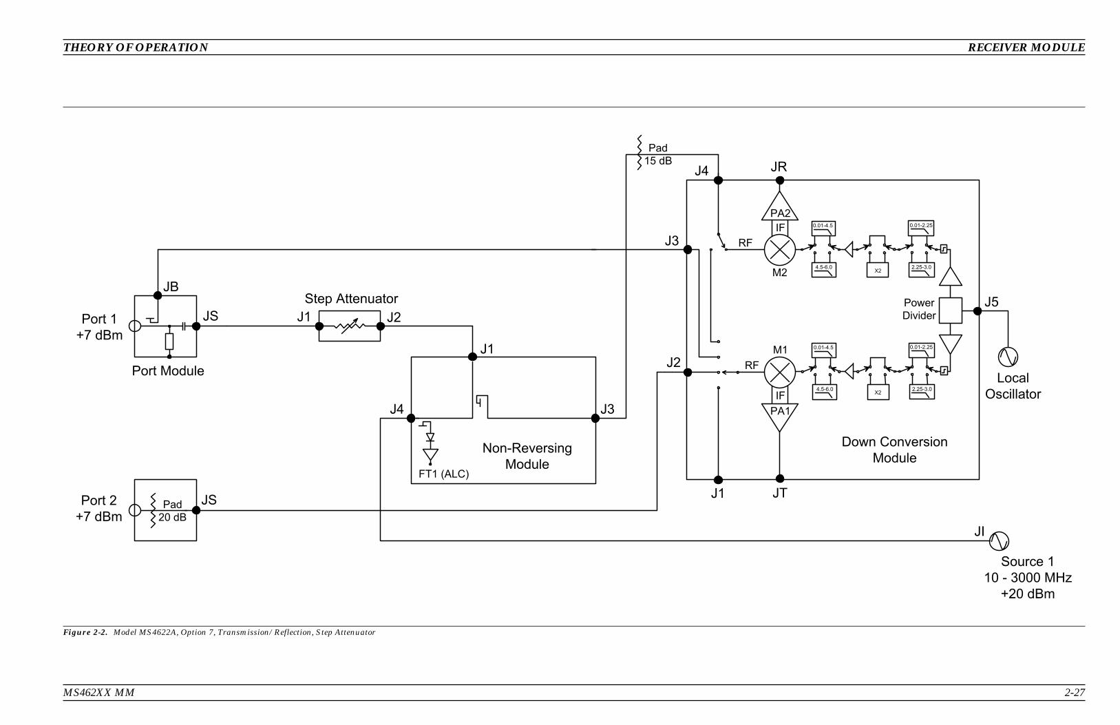
MS462XX MM 2-27
THEORY OF OPERATION RECEIVER MODULE
Figure 2-2. Model MS4622A, Option 7, Transmission/Reflection, Step Attenuator

2-28 MS462XX MM
RECEIVER MODULE THEORY OF OPERATION
Figure 2-3. Model MS4622A, Transmission/Reflection

MS462XX MM 2-29
THEORY OF OPERATION RECEIVER MODULE
Figure 2-4. Model MS4622B, Auto-Reversing

2-30 MS462XX MM
RECEIVER MODULE THEORY OF OPERATION
Figure 2-5. Model MS4622B, Auto-Reversing, 3-Port

MS462XX MM 2-31
THEORY OF OPERATION RECEIVER MODULE
Figure 2-6. Model MS4622B, Auto-Reversing, Option 4 Noise Figure

2-32 MS462XX MM
RECEIVER MODULE THEORY OF OPERATION
Figure 2-7. Model MS4622B, Auto-Reversing, Options 3A and 4

MS462XX MM 2-33
THEORY OF OPERATION RECEIVER MODULE
Figure 2-8. Model MS4622B, Auto-Reversing, Option 6, 3-Port

2-34 MS462XX MM
RECEIVER MODULE THEORY OF OPERATION
Figure 2-9. Model MS4623A/MS4624A, Transmission/Reflection, Step Attenuator, Option 7 * Refer to Figure 2-22 (page 2-47) for a functional block diagram of the Source Tripler and 9 GHz Down Conversion Module used on the model MS4624A.

MS462XX MM 2-35
THEORY OF OPERATION RECEIVER MODULE
Figure 2-10. Model MS4623A/MS4624A, Transmission/Reflection * Refer to Figure 2-22 (page 2-47) for a functional block diagram of the Source Tripler and 9 GHz Down Conversion Module used on the model MS4624A.

2-36 MS462XX MM
RECEIVER MODULE THEORY OF OPERATION
Figure 2-11. Model MS4623B/MS4624B, Auto-Reversing * Refer to Figure 2-22 (page 2-47) for a functional block diagram of the Source Tripler and 9 GHz Down Conversion Module used on the model MS4624B.

MS462XX MM 2-37
THEORY OF OPERATION RECEIVER MODULE
Figure 2-12. Model MS4623B/MS4624B, Auto-Reversing, Option 3B, 2nd Internal Source and 3rd Test Port * Refer to Figure 2-22 (page 2-47) for a functional block diagram of the Source Tripler and 9 GHz Down Conversion Module used on the model MS4624B.

2-38 MS462XX MM
RECEIVER MODULE THEORY OF OPERATION
Figure 2-13. Model MS4623B/MS4624B, Auto-Reversing, Option 4, Noise Figure * Refer to Figure 2-22 (page 2-47) for a functional block diagram of the Source Tripler and 9 GHz Down Conversion Module used on the model MS4624B.

MS462XX MM 2-39
THEORY OF OPERATION RECEIVER MODULE
Figure 2-14. Model MS4623B/MS4624B, Auto-Reversing, Option 6, 3rd Test Port * Refer to Figure 2-22 (page 2-47) for a functional block diagram of the Source Tripler and 9 GHz Down Conversion Module used on the model MS4624B.

2-40 MS462XX MM
RECEIVER MODULE THEORY OF OPERATION
Figure 2-15. Model MS4623B/MS4624B, Auto -Reversing, Options 3B and 4 * Refer to Figure 2-22 (page 2-47) for a functional block diagram of the Source Tripler and 9 GHz Down Conversion Module used on the model MS4624B.

MS462XX MM 2-41
THEORY OF OPERATION RECEIVER MODULE
Figure 2-16. Model MS4622C, Direct Access Receiver
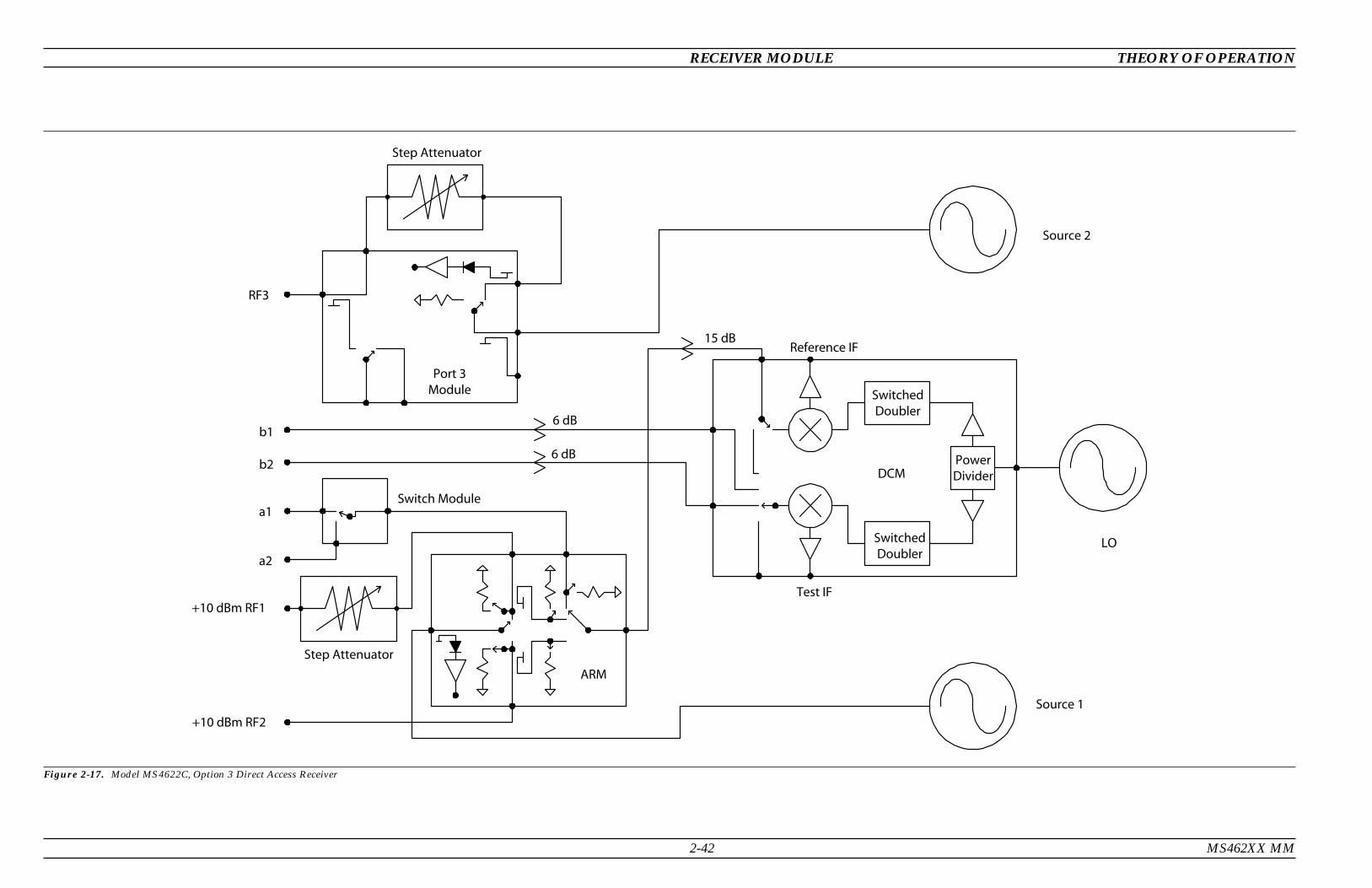
2-42 MS462XX MM
RECEIVER MODULE THEORY OF OPERATION
Figure 2-17. Model MS4622C, Option 3 Direct Access Receiver
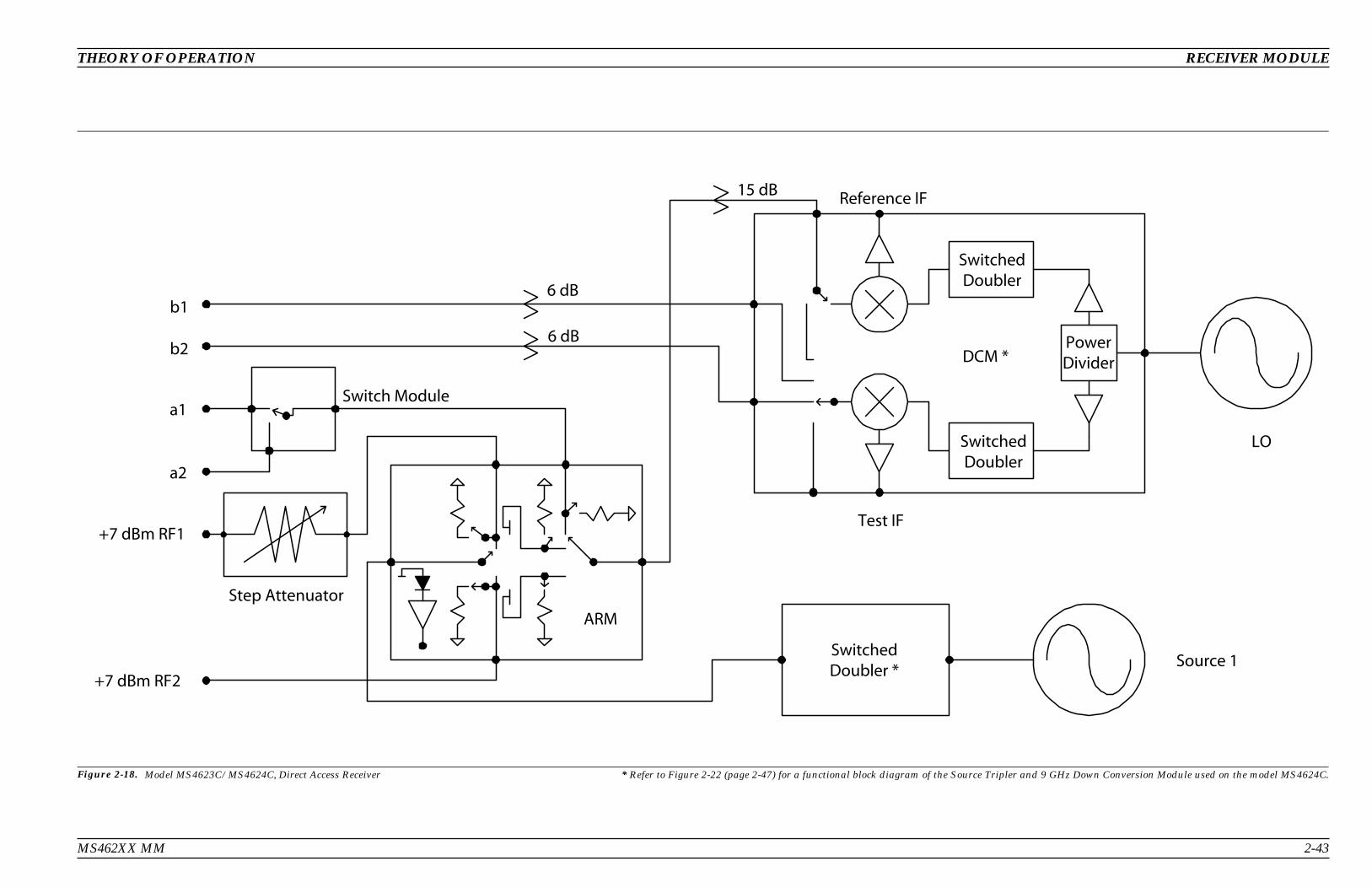
MS462XX MM 2-43
THEORY OF OPERATION RECEIVER MODULE
Figure 2-18. Model MS4623C/MS4624C, Direct Access Receiver * Refer to Figure 2-22 (page 2-47) for a functional block diagram of the Source Tripler and 9 GHz Down Conversion Module used on the model MS4624C.

2-44 MS462XX MM
RECEIVER MODULE THEORY OF OPERATION
Figure 2-19. Model MS4623C/MS4624C, Option 3 Direct Access Receiver * Refer to Figure 2-22 (page 2-47) for a functional block diagram of the Source Tripler and 9 GHz Down Conversion Module used on the model MS4624C.
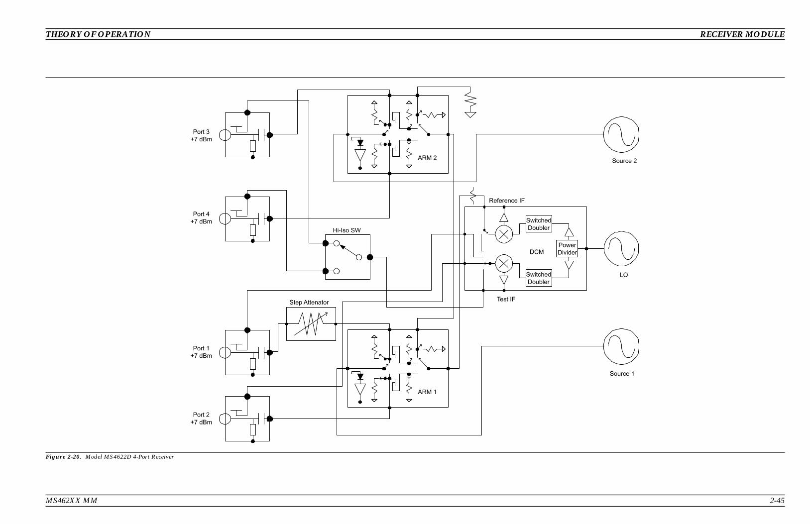
MS462XX MM 2-45
THEORY OF OPERATION RECEIVER MODULE
Figure 2-20. Model MS4622D 4-Port Receiver
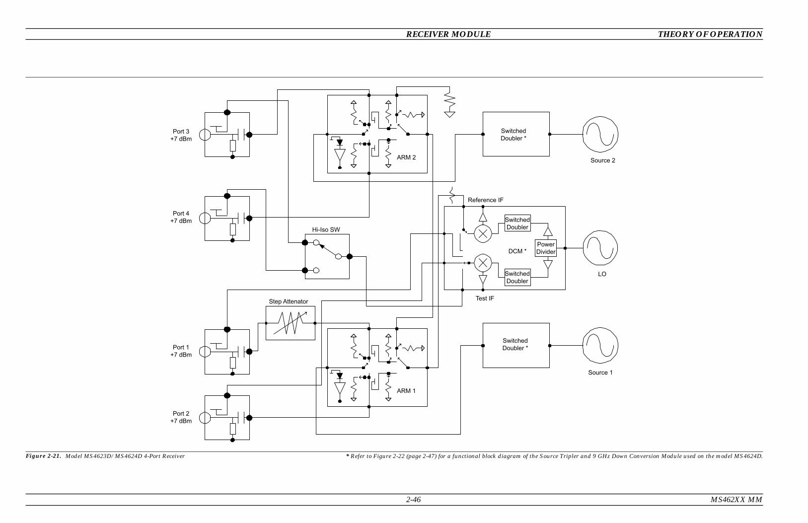
2-46 MS462XX MM
RECEIVER MODULE THEORY OF OPERATION
Figure 2-21. Model MS4623D/MS4624D 4-Port Receiver * Refer to Figure 2-22 (page 2-47) for a functional block diagram of the Source Tripler and 9 GHz Down Conversion Module used on the model MS4624D.

THEORY OF OPERATION RECEIVER MODULE BLOCK DIAGRAMS
MS462XX MM 2-47/2-48
Figure 2-22. Switched Tripler and 9 GHz Down Conversion Module Functional Block Diagrams


Table of Contents
3-1 INTRODUCTION . . . . . . . . . . . . . . . . . . . . . . . . . . . . . . . . . . . 3-3
3-2 CHECKING THE SERVICE LOG/SELF-TEST . . . . . . . . . . . . . . . . . . . 3-3
3-3 VERIFYING OUTPUT POWER ACCURACY . . . . . . . . . . . . . . . . . . . . 3-5
3-4 NON-RATIO PARAMETER TEST (MS462XA/C/D) . . . . . . . . . . . . . . . . . 3-7
3-5 SYSTEM DYNAMIC RANGE TEST (MS462XA/B/D) . . . . . . . . . . . . . . . 3-10
3-6 SYSTEM DYNAMIC RANGE TEST (MS462XC) . . . . . . . . . . . . . . . . . . 3-14
3-7 COMPRESSION LEVEL TEST (MS462XC) . . . . . . . . . . . . . . . . . . . . 3-16
3-8 RECEIVER MAGNITUDE DISPLAY LINEARITY TEST (MS462XC) . . . . . . 3-19
3-9 NOISE FIGURE MEASUREMENT CAPABILITY (OPTION 4) . . . . . . . . . . 3-26Noise Figure Assurance Check . . . . . . . . . . . . . . . . . . . . . . . . . 3-26Raw Receiver Noise Figure Check . . . . . . . . . . . . . . . . . . . . . . . . 3-26
3-10 NOISE FIGURE MEASUREMENT CONFIDENCE CHECK . . . . . . . . . . . 3-30
3-11 FREQUENCY TRANSLATING GROUP DELAY (OPTION 5) . . . . . . . . . . . 3-35
3-12 37SF50 PHASE HARMONIC STANDARDS OPERATIONAL CHECK . . . . . . 3-36Input and Output Return Loss Check . . . . . . . . . . . . . . . . . . . . . . 3-36
3-13 HARMONIC OUTPUT CHECK . . . . . . . . . . . . . . . . . . . . . . . . . . . 3-39
Chapter 3Operational PerformanceTests

Chapter 3Operational PerformanceTests
3-1 INTRODUCTION The tests in this chapter provide a means of partially testing theMS462XX system for proper operation. These tests should be performedin their entirety at least once annually. For best results, the tests shouldbe performed in the sequence presented.
3-2 CHECKING THESERVICELOG/SELF-TEST
Checking the service log consists of viewing the entries written into thelog.
Procedure: 1. Press the Utility key.
MS462XX MM 3-3
NOTE
The procedures in this chapter, along with the Verification Tests in Chapter 4, willfully test the operational status of the MS462XX.
CAUTION
The service log contains historical information about instrument condition andany failures that may have occurred. It should be cleared only by a qualifiedservice personnel. Such clearing should be accomplished only upondetermining that the errors need not be saved to disk, or printed out for servicepurposes.

2. Select:
DIAGNOSTICS
SERVICE LOG
The MS462XX will now display the contents of the service log. The dis-play consists of a header and an error listing. The header contains a vari-ety of system service information. The error listing contains error mes-sages for failures that may have occurred during operation.
3. Select:
SELF TEST
The self test performs a series of tests that verify that various internalMS462XX circuits are functional and operating properly.
4. Press the Utility key.
5. Select:
DIAGNOSTICS
START SELF TEST
6. Wait for the test sequence to complete.Once invoked, this test requires no user interaction or externalequipment.
Upon completion, the net pass/fail result of the self test is shown on theLCD display. If the MS462XX is in remote-only operation, the results arereported via the GPIB output buffer. If the self test fails, detailed errormessages will be written into the service log.
NOTEThe self-test does not check the RF signal path in theVNMS. RF signals must be tested manually as described inthe following sections of this chapter.
If the self test fails:
� Check the service log to view the failure messages.� Proceed to Chapter 6—Troubleshooting.
CHECKING THE SERVICE LOG/SELF-TEST PERFORMANCE TESTS
3-4 MS462XX MM
CAUTION
The CLEAR LOG softkey select ion wil limmediately andpermanently clear allthe error messageentr ies from theservice log.(However, it will notclear the headerinformation.)

3-3 VERIFYINGOUTPUT POWERACCURACY
These procedures use the Power ALC Verification built-in function of theMS462XX Basic Measurement Software. The Standard Conditions andSpecial Precautions described in Section 4-2 should be observed whenperforming these procedures.
EquipmentRequired:
The following test equipment is required:
� Anritsu ML243XA Power Meter� Anritsu MA247XA Power Sensor� Anritsu 2100-2 GPIB Cable� Various Adapters
Procedure: 1. Set up the equipment as shown in Figure 3-1 below.
2. Turn on the instrument and allow it to warm-up (refer to Section 2-2for more explanation).
3. Press the Utility key
4. Select:
DIAGNOSTICS
TROUBLESHOOTING
MORE
VERIFY ALC CALIBRATION
5. Calibrate and zero the power sensor.
6. Connect the power sensor to Port 1 and select the START VERIFICA-TION soft key.
PERFORMANCE TESTS VERIFYING OUTPUT POWER ACCURACY
MS462XX MM 3-5
NoiseIn
Noise+28V
NO OPERATOR SERVICE-ABLE PARTS INSIDE.REFER SERVICING TOQUALIFIED PERSONNEL.
WARNING
CAUTIONFOR CONTINUED FIREPROTECTION REPLACEONLY WITH SPECIFIEDTYPE AND RATED FUSE.
IEEE 488.2GPIB
DedicatedGPIB
Serial Port Ethernet VGA SCSI-2
ExtAnalogOutput
ExtTrigger
LPT Line Printer Ext I/O
Port 1Port 2BiasBias
Port 2Bias Fuse
Port 1Bias Fuse
Ext AnalogIn
ExtSource
Ext 10 MHzIn
47-440 Hz85-264VAC
REPLACE FUSE ONLY WITHSAME TYPE AND RATING
CAUTIONDO NOT OPERATE
WITH POWER CORDUNGROUNDED
N274
00000001Made in UK
12-24V DC
(1.3A)
OUTPUT 1 OUTPUT 2 INPUT 1
DIGITAL
INPUT 2
ANALOG
CALIBRATORB
RS 232
PARALLEL PRINTER
GPIB / IEEE 488
CAUTIONDO NOT OPERATEWITH UNGROUNDEDPOWER CORD.
85-250 VAC
47-440Hz40VA MAX
SEE MANUAL FOR VOLTAGE RANGES ON BNC CONNECTORS
A
NO OPERATOR SERVICE-ABLE PARTS INSIDE.
WARNING
Figure 3-1. ML2430A Series Power Meter GPIB connection to the MS462XX Vector Network Measurement System

7. Verify that the instrument passes this test.
8. If the instrument is a MS462XB/C with Option 3 installed or aMS462XD, press the SELECT SOURCE soft key to select source 2.
9. Connect the power sensor to Port 3 and select the START VERIFICA-TION soft key.
10. Verify that the instrument passes this test.
11. Select the menu soft key as follows to exit the TROUBLESHOOTINGmode:
RETURN
RETURN
FINISHED, RECOVER FROM TROUBLESHOOTING
VERIFYING OUTPUT POWER ACCURACY PERFORMANCE TESTS
3-6 MS462XX MM
NOTE
The worst case testresul t wi l l bedisplayed on thescreen when theinstrument fails thistest only. The failedtest result is alsorecorded in theService Log.
CAUTION
The TROUBLESHOOTING function must be properly exited to restorenormal system operation.
3-4 NON-RATIOPARAMETER TEST(MS462XA/C/D)
One of the most useful tests for troubleshooting RF component problemsin the Receiver Module is the non-ratio parameter test. This test verifiesthat each individual receiver channel operates properly as well as pro-vides clues to where a problem is located.
NOTEThe non-ratio parameter test is not available for theMS462XC.
Test Setup: Connect the test equipment as described below.
� Connect Ports 1 and 2 together using a high quality throughline.� Press the Default key, then the 0 key to reset the MS462XX to its
factory-default settings.
Test Procedure: Display the non-ratio parameters as follows:
1. Press the Display key and select:
GRAPH TYPE
LOG MAGNITUDE
RETURN
SCALE
RESOLUTION
5 X1
RETURN
DISPLAY MODE
SINGLE CHANNEL
2. Press the Meas key and select:
S21, TRANS b2/a1
USER DEFINED
3. Press S21/USER X to activate USER X.USER X becomes red (the actual user number “X” is not significant).
4. Select:
CHANGE RATIO
a1 (Ra) as the numerator
1 (UNITY) as the denominator
5. For the model under test, ensure that the minimum value of the RFdisplay is greater than the minimum level shown for a1/1 in Ta-ble 3-1 (page 3-8). Figure 3-2 on page 3-9 shows an example of a typ-ical non-ratio display.
PERFORMANCE TESTS NON-RATIO PARAMETER TEST (MS462XA/C/D)
MS462XX MM 3-7

6. Change the user defined ratio by selecting:
CHANGE RATIO
MORE
b2 (Tb) as the numerator
1 (UNITY) as the denominator
7. Ensure thta the minimum level of b2/1 is above the level shown inTable 3-1.
NON-RATIO PARAMETER TEST (MS462XA/C/D) PERFORMANCE TESTS
3-8 MS462XX MM
ModelBeginning
S-ParameterDevice to
InstallUser Defined
RatioMinimum
Level
MS4622AS21
Thru fromPort 1 toPort 2
a1/1 -6 dB
S21 b2/1 -12 dB
MS4623A S21 a1/1 -8 dB
S21 b2/1 -13 dB
MS4624AS21 a1/1 -15 dB
S21 b2/1 -15 dB
MS4622B
S21Thru fromPort 1 toPort 2
a1/1 -7 dB
S21 b2/1 -18 dB
S12 a2/1 -7 dB
S12 b1/1 -18 dB
S33 Short onPort 3
a3/1 -7 dB
S33 b3/1 -18 dB
MS4623B
S21Thru fromPort 1 toPort 2
a1/1 -8 dB
S21 b2/1 -15 dB
S12 a2/1 -8 dB
S12 b1/1 -10 dB
S33 Short onPort 3
a3/1 -8 dB
S33 b3/1 -11 dB
MS4624B
S21Thru fromPort 1 toPort 2
a1/1 -15 dB
S21 b2/1 -20 dB
S12 a2/1 -15 dB
S12 b1/1 -15 dB
S33 Short onPort 3
a3/1 -15 dB
S33 b3/1 -15 dB
MS4624D
S21Thru fromPort 1 toPort 2
a1/1 -15 dB
S21 b2/1 -15 dB
S12 a2/1 -15 dB
S12 b1/1 -15 dB
S33 Short onPort 3
a3/1 -15 dB
S33 b3/1 -20 dB
S44 Short onPort 4
a4/1 -15 dB
S44 b4/1 -20 dB
Table 3-1. Minimum Amplitude Specifications

8. Measure all other non-ratio parameters shown in Table 3-1 by se-lecting the S-parameters S12, S33 or S44 and setting up the user de-fined ratios as described in Steps 2 through 6. Also, install a shorton Ports 3 and 4 as indicated in Table 3-1.
NOTEViewing Port 3 and Port 4 with a short attached will cause asignificant ripple on the RF display. This is normal.
The non-ratio parameters test results reveal where the fault may be lo-cated.
For example, if the non-ratio parameters test results for a MS462XBshows that b2/1 has a glitch appearing on the frequency response trace,but a1/1 and b1/1 are okay, then the fault is possibly in the Port 2 moduleor the cable connected between the Port 2 module and the Down Conver-sion Module.
PERFORMANCE TESTS NON-RATIO PARAMETER TEST (MS462XA/C/D)
MS462XX MM 3-9
NOTE
If desired, use theReadout Markersfunction (Marker keyand Readout Markersoft key) to obtainprecise frequencyand ampl i tudevalues.
Figure 3-2. Non-Ratioed Parameters Waveforms
3-5 SYSTEM DYNAMICRANGE TEST(MS462XA/B/D)
This section verifies that the VNMS has a dynamic range consistent withfactory specifications. A full 12-term calibration (with isolation) must beperformed.
EquipmentRequired:
The following equipment is required:
� Anritsu Calibration kit intended for use with the instrument un-der test
� RF cables or Anritsu throughlines suitable for use with the in-strument
Procedure: 1. Set the instrument to the factory default parameters by pressing theDefault key, then the 0 key.
2. Install a cable or throughline to Port 1.
3. If the Cal Kit has a coefficient disk, insert the disk into the floppydrive of the VNMS.
4. Load the coefficients into the VNMS by pressing the CAL key andselecting:
MORE
COMPONENT UTILITIES
INSTALL KIT INFO FROM DISK
5. Press the CAL key, then select:
MANUAL CAL
2 PORT
NEXT CAL STEP
FULL 12-TERM
INCLUDE ISOLATION (STANDARD)
N-DISCRETE FREQUENCIES
6. Enter a start frequency of 100 MHz, an increment of 100 MHz, andthe number of points of 30 (3 GHz units), 60 (6 GHz units), or 90(9 GHz units).
7. Select:
FILL THE RANGE
INDIVIDUAL FREQ INSERT
INSERT NEXT FREQUENCY
RETURN
8. Select NEXT CAL STEP to resume the calibration.
SYSTEM DYNAMIC RANGE TEST (MS462XA/B/D) PERFORMANCE TESTS
3-10 MS462XX MM
9. Ensure the correct test port connector types are selected. If not, se-lect the port connection displayed and choose the correct type fromthe list.
10. Select START CAL and continue to use the default settings for thecalibration.
11. Before measuring the isolation devices (50 � terminations), pressthe Avg key.
12. Select DATA AVERAGE and enter 10 (followed by the X1 key).
13. Select:
I.F. BANDWIDTH
I.F. BW 10 Hz
14. Install the isolation devices (50 � terminations) from the Cal Kit toPort 1 and Port 2.
15. Select the MEASURE BOTH PORTS soft key.
16. Continue the calibration by following the on-screen directions andby selecting the following soft keys until the calibration is complete:
NEXT CAL STEP
MEASURE BOTH PORTS or
MEASURE DEVICE(S)
17. The calibration is complete when the following message is displayed(press the Enter key):
PRESS <ENTER> TO PROCEED
18. Install the 50 ohm terminations from the Cal Kit to Port 1 andPort 2.
19. Press the Avg key and set the number of averages to 10 and theI.F. BW to 10 Hz by selecting:
AVERAGE ON
DATA AVERAGE
10
X1
SELECT I.F. BANDWIDTH
I.F. BW 10 Hz
PERFORMANCE TESTS SYSTEM DYNAMIC RANGE TEST (MS462XA/B/D)
MS462XX MM 3-11

20. Press the Display key and select:
GRAPH TYPE
LOG MAGNITUDE
RETURN
SCALE
RESOLUTION
21. Enter 10 and press the X1 key.
22. Select REFERENCE VALUE and enter -70, then press the X1 key.Reference line 7 and select RETURN.
23. Select:
DISPLAY MODE
SINGLE CHANNEL
24. Press the Meas key and select:
S21, TRANS b2/a1
25. Press the Marker key and select:
DISPLAY MARKERS ON
READOUT MARKERS
26. Set the markers as follows:
MARKER 1: 10MHz
MARKER 2: 400 GHz
MARKER 3: 3 GHz
MARKER 4: 6 GHz
MARKER 5: 9 GHz
MARKER 6: Any frequency
27. Allow the instrument to complete a full sweep. Using the knob tomove Marker 6, view the Marker 6 readout and find the highestpoint between subsequent markers. Ensure that the values of thehighest points are below the values shown in Table 3-2.
28. If the instrument has two ports, the Dynamic Range test is finished.
29. If the instrument has three or four ports, calibrate for S13 as fol-lows:
30. Press the Cal key, then select:
MANUAL CAL
3 PORT
NEXT CAL STEP
SYSTEM DYNAMIC RANGE TEST (MS462XA/B/D) PERFORMANCE TESTS
3-12 MS462XX MM

31. Set up the calibration using all default parameters.
32. Before measuring the Isolation Devices, press the Avg key and select10 averages and 10 Hz I.F. BW (as in Steps 12 and 13). Measure theIsolation Devices.
33. Finish the calibration and install terminations to Ports 1 and 3.
34. Press the Meas key and select S13.
35. Press the Avg key, ensure that averaging is ON and select:
AVERAGES=10
IF BANDWIDTH=10 Hz.
36. Allow the instrument to complete a full sweep. Move Marker 6 tofind the highest points in the RF display and ensure that the specifi-cations in Table 3-2 for S13 are met.
37. If the instrument has 3 ports, the test is finished.If the instrument has 4 ports, press the Cal key and perform a 4 portcalibration using all default parameters.
38. Before measuring the isolation devices, press the Avg key and select:
AVERAGES=10
I.F. BANDWIDTH =10 Hz
39. After the calibration is finished, install the terminations on Ports 1and 4. Press the Meas key and select S14.
40. Repeat Steps 35 and 36 for S14, and verify that the specificationsshown on Table 3-2 are met.
The system dynamic range operational check is complete.
PERFORMANCE TESTS SYSTEM DYNAMIC RANGE TEST (MS462XA/B/D)
MS462XX MM 3-13
Model S-Parameter10 MHz to400 MHz
400 MHz to3 GHz
3 GHz -to6 GHz
6 GHz to9 GHz
All A, B, DModels
S21 -90 dB * -100 dB -90 dB -90 dB
All A, B, DModels
S13 -90 dB * -100 dB -90 dB -90 dB
All A, B, DModels
S14 -90 dB * -100 dB -90 dB -90 dB
* On 9 GHz models, -80 dB is typical at 10 MHz
Table 3-2. Dynamic Range Specifications for 10Hz IF Bandwidth

3-6 SYSTEM DYNAMICRANGE TEST(MS462XC)
This test verifies the System Dynamic Range of the test channels of thereceiver.
Test Setup: Set up the equipment as shown below and allow the instruments towarm-up for at least one hour.
Procedure: 1. Press the Default key, then the 0 key to reset the MS462XC.
2. Press the Ch 3 key, then the Display key and select:
DISPLAY MODE
SINGLE CHANNEL
RETURN
GRAPH TYPE
LOG MAGNITUDE
3. Press the Config key.
4. Select DATA POINTS and change the value to 51MAX PTS.
5. Press the Power key and select:
SOURCE 1 SETUP
FLAT TEST PORT POWER CAL
6. Change POWER TARGET to �10 dBm.
7. Zero and calibrate the power meter. Then connect the power sensorto the unterminated end of the model 43KC-10 fixed attenuator.
SYSTEM DYNAMIC RANGE TEST (MS462XC) PERFORMANCE TESTS
3-14 MS462XX MM
Data Entry
PowerKeyboard
Port 3
Channels Enhancement
Stimulus System
Port 1 Port 2
Probe Power
1
8
5
2
9
6
3
-.
G/ns/m
M/ s/cm�
k/ms/mm
X1
Enter
Local
Appl
Meas
Marker
Hold
Ch 1 Ch 2
Ch 4Ch 3
Freq Sweep
Power Config
Seq Cal
Avg Utility
HardCopy
DefaultSave /Recall
0
7
4
Display
Clr
NoiseIn
Noise+28V
NO OPERATOR SERVICE-ABLE PARTS INSIDE.REFER SERVICING TOQUALIFIED PERSONNEL.
WARNING
CAUTIONFOR CONTINUED FIREPROTECTION REPLACEONLY WITH SPECIFIEDTYPE AND RATED FUSE.
IEEE 488.2GPIB
DedicatedGPIB
Serial Port Ethernet VGA SCSI-2
ExtAnalogOutput
ExtTrigger
LPT Line Printer Ext I/O
Ext AnalogIn
ExtSource
Ext 10 MHzIn
47-440 Hz85-264VAC
REPLACE FUSE ONLY WITHSAME TYPE AND RATING
CAUTIONDO NOT OPERATE
WITH POWER CORDUNGROUNDED
N274
A1 B1A2 B2
MS46XC Rear Panel
MS462XC Front Panel
AnritsuPower Meter
Power Sensor
b1 b2
Coaxial Cable
Dedicated GPIB GPIB Cable
Port 1 *Connect dashed lines as directed by procedure
43KC-10Attenuator
*
Cal / Zero
ML2408A Power Meter
ON / OFF
Sensor Channel Trigger System
CALIBRATOR
0
1
4
7
2
5
8
+ / -
3
6
9
CLR
A
B
Figure 3-3. Test Equipment Setup for System Dynamic Range Test

8. Press the BEGIN CAL soft key to start calibration.
9. After the Flat Test Port Power Cal is completed, disconnect thepower sensor from the unterminated end of the 43KC-10 attenuatorand connect the attenuator with the coaxial cable to b1 input on therear panel of MS462XC.
10. Press the Avg key and select:
SELECT I.F. BANDWIDTH
I.F. BW 10 Hz
11. Press the Meas key and select:
USER DEFINED
CHANGE RATIO
b1 (Ta)
1 (UNITY)
12. Press the S21/USER 1 soft key to select USER 1.
13. Press the Display key and select the TRACE MEMORY soft key.
14. Allow two complete sweeps to occur, the select:
STORE DATA TO MEMORY
DATA (/) MEMORY
RETURN
SCALE
15. Disconnect the 43KC-10 attenuator with the cable from the receiverinput. Then connect a termination to the receiver input.
16. Change the REFERENCE VALUE to � 97 dB.
17. Allow one full sweep to occur, then press the Hold key.
18. Verify that the trace is below the REFERENCE VALUE.
19. Press the Meas key and select:
USER DEFINED
CHANGE RATIO
b2 (Tb)
1 (UNITY)
20. Remove the 43K-10 Attenuator with the coaxial cable from b1 inputand connect to b2 input.
21. Repeat Steps 13 to 18.
PERFORMANCE TESTS SYSTEM DYNAMIC RANGE TEST (MS462XC)
MS462XX MM 3-15

3-7 COMPRESSIONLEVEL TEST(MS462XC)
This test verifies the compression magnitude levels of the MS462XC Vec-tor Network Measurement System receiver.
Test Setup: Set up the equipment as shown below and allow the instruments towarm-up for at least one hour.
Procedure: 1. Press the Default key, then the 0 key to reset the instrument.
2. Press the Ch 3 key, then the Display key.
3. Select:
DISPLAY MODE
SINGLE CHANNEL
RETURN
GRAPH TYPE
LOG MAGNITUDE
4. Press the Freq key.
5. Select:
DISCRETE FILL
INDIVIDUAL FREQ INSERT
6. Select AUTO INCR to turn this function off.
7. Select the NEXT FREQUENCY soft key. Enter 50 MHz and select theINSERT NEXT FREQUENCY soft key.
COMPRESSION LEVEL TEST (MS462XC) PERFORMANCE TESTS
3-16 MS462XX MM
Data Entry
PowerKeyboard
Port 3
Channels Enhancement
Stimulus System
Port 1 Port 2
Probe Power
1
8
5
2
9
6
3
-.
G/ns/m
M/ s/cm�
k/ms/mm
X1
Enter
Local
Appl
Meas
Marker
Hold
Ch 1 Ch 2
Ch 4Ch 3
Freq Sweep
Power Config
Seq Cal
Avg Utility
HardCopy
DefaultSave /Recall
0
7
4
Display
Clr
NoiseIn
Noise+28V
NO OPERATOR SERVICE-ABLE PARTS INSIDE.REFER SERVICING TOQUALIFIED PERSONNEL.
WARNING
CAUTIONFOR CONTINUED FIREPROTECTION REPLACEONLY WITH SPECIFIEDTYPE AND RATED FUSE.
IEEE 488.2GPIB
DedicatedGPIB
Serial Port Ethernet VGA SCSI-2
ExtAnalogOutput
ExtTrigger
LPT Line Printer Ext I/O
Ext AnalogIn
ExtSource
Ext 10 MHzIn
47-440 Hz85-264VAC
REPLACE FUSE ONLY WITHSAME TYPE AND RATING
CAUTIONDO NOT OPERATE
WITH POWER CORDUNGROUNDED
N274
A1 B1A2 B2
MS46XC Rear Panel
MS462XC Front Panel
Anritsu Power Meter
Power Sensor
Coaxial Cable
Port 1
a1
a2 b1
b2
*Connect dashed lines as directed by procedure
43KC-10Attenuator
*
Cal / Zero
ML2408A Power Meter
ON / OFF
Sensor Channel Trigger System
CALIBRATOR
0
1
4
7
2
5
8
+ / -
3
6
9
CLR
A
B
Figure 3-4. Test Equipment Setup for Compression Test

8. Select the NEXT FREQUENCY soft key, then enter the following fre-quencies:
� MS4622C—1 GHz, 2 GHz, and 3 GHz� MS4623C—1 GHz, 2 GHz, 4 GHz, and 6 GHz� MS4624C—1 GHz, 2 GHz, 4 GHz, 6 GHz and 9 GHz
9. Select:
RETURN
RETURN to exit this setup menu.
10. Select the C.W. MODE soft key to turn C.W. mode ON.
11. Change the C.W. frequency to 50 MHz.
12. Press the Config key and select the DATA POINTS soft key. ChangePOINTS DRAWN IN C.W. to 51 POINT(S).
13. Press the Meas key and select USER DEFINED.
14. Select:
CHANGE RATIO
b1 (Ta)
1 (UNITY)
15. Press the S11/USER 1 soft key to select USER 1.
16. Press the Marker key.
17. Select:
MARKER READOUT
18. Select the marker soft key to turn on Marker 1, then use the nu-meric data entry key to change POINT to 25.
19. Press the Marker key again.
20. Select the SCREEN DISPLAY soft key to ON.
21. Zero and calibration the power sensor.
22. Set the power sensor CAL FACTOR for the frequency being mea-sured; that is, 50 MHz, 1 GHz etc.
23. Connect the power sensor to the unterminated end of the 43KC-10fixed attenuator with cable linked to Port 1.
24. Press the Power key and select SOURCE 1 SETUP. Adjust SOURCE1 POWER so that the power meter reads –10 dBm �0.01 dB.
PERFORMANCE TESTS COMPRESSION LEVEL TEST (MS462XC)
MS462XX MM 3-17
NOTE
Select the INSERTNEXT FREQUENCYsoft key to store theentered frequencyvalue to memory.

25. Record the SOURCE 1 POWER setting in the corresponding space inTable 3-4 (page 3-23) for MS4622C, Table 3-5 (page 3-24) forMS4623C, or Table 3-6 (page 3-25) for MS4624C.
26. Adjust SOURCE 1 POWER so that the power meter reads –20 dBm� 0.01 dB.
27. Record the SOURCE 1 POWER setting to the corresponding spacein Table 3-4 for MS4622C, Table 3-5 for MS4623C, or Table 3-6 forMS4624C.
28. Connect the unterminated end of the fixed attenuator (with cablelinked to Port 1) to b1 input.
29. Press the Display key and select the TRACE MEMORY soft key.
30. Allow two complete sweeps to occur.
31. Select:
STORE DATA TO MEMORY
DATA (/) MEMORY
RETURN
32. Press the Power key and select SOURCE 1 SETUP. Set the SOURCE1 POWER to the level recorded in Step 25., 25.
33. Verify that: 10 dB - Marker 1 Readout � 0.1 dB
34. Set the SOURCE 1 POWER to the level recorded in Step 27., 27.
35. Repeat Steps 28 through 33 for b2, a1, and a2 inputs.
36. Repeat Steps 23 through 34 for the next frequency point as listed inTable 3-4 for MS4622C, Table 3-5 for MS4623C, or Table 3-6 forMS4624C.
COMPRESSION LEVEL TEST (MS462XC) PERFORMANCE TESTS
3-18 MS462XX MM
NOTES
Move the fixed attenuator with cable linked to Port 1 to the next receiverinput (i.e., b2, a1, or a2).
Change the USER DEFINED setting the corresponding user definedratio (i.e., b2/1, a1/1 or a2/1).

3-8 RECEIVERMAGNITUDEDISPLAYLINEARITY TEST(MS462XC)
This test verifies the magnitude linearity of the MS462XC receiver.
Test Setup: Set up the equipment as directed in the procedure below and allow the in-struments to warm-up for at least one hour.
Procedure: 1. Press the Default key and then 0 key to reset the instrument.
2. Press the Ch 3 key and then Display key.
3. Select:
DISPLAY MODE
SINGLE CHANNEL
RETURN
GRAPH TYPE
LOG MAGNITUDE
4. Press the Freq key and select the START FREQUENCY soft key.
5. Change START FREQUENCY to 50 MHz.
6. Select the C.W. MODE soft key to turn C.W. mode ON.
7. Verify that the C.W. frequency is 50 MHz.
8. Press the Config key and select the DATA POINTS soft key. ChangePOINTS DRAWN IN C.W. to 51 POINT(S).
9. Press the Avg key.
10. Select:
SELECT I.F. BANDWIDTH
I.F. BW 10 Hz
11. Press the Meas key and select USER DEFINED.
12. Select:
CHANGE RATIO
b1 (Ta)
1 (UNITY)
13. Press the S21/USER 1 soft key to select USER 1.
14. Press the Marker key.
PERFORMANCE TESTS RECEIVER MAGNITUDE DISPLAY LINEARITY TEST(MS462XC)
MS462XX MM 3-19

15. Select:
MARKER READOUT
16. Use the soft key to turn on Marker 1. Then use the numeric data en-try key to change POINT to 25.
17. Press the Marker key again.
18. Select the SCREEN DISPLAY soft key to ON.
19. Zero and calibrate the power sensor.
20. Set the power sensor CAL FACTOR for the frequency being mea-sured.
21. Connect the power sensor to the BNC male end of the adapter con-nected to the 43KC-10 fixed attenuator (Figure 3-5).
22. Press the Power key and select SOURCE 1 SETUP. Adjust SOURCE1 POWER so that the power meter reads �15 dBm �0.1 dB.
23. Disconnect the power sensor from the BNC male end of the adapterthat is connected to the 43KC-10 fixed attenuator (Figure 3-6).
RECEIVER MAGNITUDE DISPLAY LINEARITY TEST (MS462XC) PERFORMANCETESTS
3-20 MS462XX MM
Data Entry
PowerKeyboard
Port 3
Channels Enhancement
Stimulus System
Port 1 Port 2
Probe Power
1
8
5
2
9
6
3
-.
G/ns/m
M/ s/cm�
k/ms/mm
X1
Enter
Local
Appl
Meas
Marker
Hold
Ch 1 Ch 2
Ch 4Ch 3
Freq Sweep
Power Config
Seq Cal
Avg Utility
HardCopy
DefaultSave /Recall
0
7
4
Display
Clr
MS462XC Front Panel
Anritsu Power Meter
Power Sensor
Coaxial Cable
SMA (f) to BNC (m)Adapter
Port 1
*Connect dashed lines as directed by procedure
*
43KC-10Attenuator
Cal / Zero
ML2408A Power Meter
ON / OFF
Sensor Channel Trigger System
CALIBRATOR
0
1
4
7
2
5
8
+ / -
3
6
9
CLR
A
B
Figure 3-5. Test Equipment Setup for Receiver Magnitude Display Linearity Test Calibration Setup 1

24. Insert a BNC female to BNC female adapter between the two BNCmale ports, as shown in Figure 3-6.
25. Press the Display key and select the TRACE MEMORY soft key.
26. Allow two complete sweeps to occur.
27. Select:
STORE DATA TO MEMORY
DATA (/) MEMORY
RETURN
PERFORMANCE TESTS RECEIVER MAGNITUDE DISPLAY LINEARITY TEST(MS462XC)
MS462XX MM 3-21
Data Entry
PowerKeyboard
Port 3
Channels Enhancement
Stimulus System
Port 1 Port 2
Probe Power
1
8
5
2
9
6
3
-.
G/ns/m
M/ s/cm�
k/ms/mm
X1
Enter
Local
Appl
Meas
Marker
Hold
Ch 1 Ch 2
Ch 4Ch 3
Freq Sweep
Power Config
Seq Cal
Avg Utility
HardCopy
DefaultSave /Recall
0
7
4
Display
Clr
NoiseIn
Noise+28V
NO OPERATOR SERVICE-ABLE PARTS INSIDE.REFER SERVICING TOQUALIFIED PERSONNEL.
WARNING
CAUTIONFOR CONTINUED FIREPROTECTION REPLACEONLY WITH SPECIFIEDTYPE AND RATED FUSE.
IEEE 488.2GPIB
DedicatedGPIB
Serial Port Ethernet VGA SCSI-2
ExtAnalogOutput
ExtTrigger
LPT Line Printer Ext I/O
Ext AnalogIn
ExtSource
Ext 10 MHzIn
47-440 Hz85-264VAC
REPLACE FUSE ONLY WITHSAME TYPE AND RATING
CAUTIONDO NOT OPERATE
WITH POWER CORDUNGROUNDED
N274
A1 B1A2 B2
MS46XC Rear Panel
MS462XC Front Panel
b1 b2
Coaxial Cable
Coaxial Cable
SMA (m) to BNC (m)Adapter
SMA (f) to BNC (m)Adapter
Port 1
*Connect the dashed lines as directed by the procedure.
CalibrationBNC (f) toBNC (f)
*
*
43KC-10Attenuator
Figure 3-6. Receiver Magnitude Display Linearity Calibration Setup 2

28. Remove the BNC female to BNC female adapter and install the stepattenuator in its place, as shown in Figure 3-7. Then set the attenu-ation to 10 dB.
29. Verify that the difference of the Marker 1 readout and the calibratedvalue of the step attenuator is within specification (refer to Ta-ble 3-3).
30. Set the step attenuator to other settings listed in Table 3-3 at theend of this chapter and repeat Step 29.
31. Press the Meas key and select USER DEFINED.
32. Select:
CHANGE RATIO
b2 (Tb)
1 (UNITY)
33. Press the S21/USER 1 soft key to select USER 1.
34. Remove the connection at b1 input and re-connect to b2 input.
35. Remove the Step Attenuator from the set up.
36. Repeat Steps 24 through 30.
RECEIVER MAGNITUDE DISPLAY LINEARITY TEST (MS462XC) PERFORMANCETESTS
3-22 MS462XX MM
Data Entry
PowerKeyboard
Port 3
Channels Enhancement
Stimulus System
Port 1 Port 2
Probe Power
1
8
5
2
9
6
3
-.
G/ns/m
M/ s/cm�
k/ms/mm
X1
Enter
Local
Appl
Meas
Marker
Hold
Ch 1 Ch 2
Ch 4Ch 3
Freq Sweep
Power Config
Seq Cal
Avg Utility
HardCopy
DefaultSave /Recall
0
7
4
Display
Clr
NoiseIn
Noise+28V
NO OPERATOR SERVICE-ABLE PARTS INSIDE.REFER SERVICING TOQUALIFIED PERSONNEL.
WARNING
CAUTIONFOR CONTINUED FIREPROTECTION REPLACEONLY WITH SPECIFIEDTYPE AND RATED FUSE.
IEEE 488.2GPIB
DedicatedGPIB
Serial Port Ethernet VGA SCSI-2
ExtAnalogOutput
ExtTrigger
LPT Line Printer Ext I/O
Ext AnalogIn
ExtSource
Ext 10 MHzIn
47-440 Hz85-264VAC
REPLACE FUSE ONLY WITHSAME TYPE AND RATING
CAUTIONDO NOT OPERATE
WITH POWER CORDUNGROUNDED
N274
A1 B1A2 B2
MS46XC Rear Panel
MS462XC Front Panel
b1 b2
Coaxial Cable
Coaxial Cable
SMA (m) to BNC (m)Adapter
SMA (f) to BNC (m)Adapter
Port 1
*Connect the dashed lines as directed by the procedure.
*
*
43KC-10Attenuator
Step Attenuator
Figure 3-7. Receiver Magnitude Display Linearity Calibration Setup 3
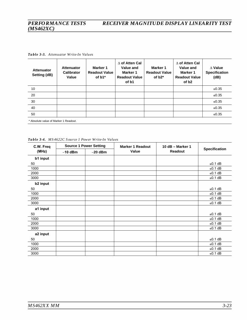
PERFORMANCE TESTS RECEIVER MAGNITUDE DISPLAY LINEARITY TEST(MS462XC)
MS462XX MM 3-23
AttenuatorSetting (dB)
AttenuatorCalibrator
Value
Marker 1Readout Value
of b1*
� of Atten CalValue andMarker 1
Readout Valueof b1
Marker 1Readout Value
of b2*
� of Atten CalValue andMarker 1
Readout Valueof b2
� ValueSpecification
(dB)
10 �0.35
20 �0.35
30 �0.35
40 �0.35
50 �0.35
* Absolute value of Marker 1 Readout.
Table 3-3. Attenuator Write-In Values
C.W. Freq
(MHz)
Source 1 Power Setting Marker 1 ReadoutValue
10 dB – Marker 1Readout
Specification�10 dBm �20 dBm
b1 input
50 �0.1 dB
1000 �0.1 dB
2000 �0.1 dB
3000 �0.1 dB
b2 input
50 �0.1 dB
1000 �0.1 dB
2000 �0.1 dB
3000 �0.1 dB
a1 input
50 �0.1 dB
1000 �0.1 dB
2000 �0.1 dB
3000 �0.1 dB
a2 input
50 �0.1 dB
1000 �0.1 dB
2000 �0.1 dB
3000 �0.1 dB
Table 3-4. MS4622C Source 1 Power Write-In Values

RECEIVER MAGNITUDE DISPLAY LINEARITY TEST (MS462XC) PERFORMANCETESTS
3-24 MS462XX MM
C.W. Freq
(MHz)
Source 1 Power Setting Marker 1 ReadoutValue
10 dB – Marker 1Readout
Specification�10 dBm �20 dBm
b1 input
50 �0.1 dB
1000 �0.1 dB
2000 �0.1 dB
4000 �0.1 dB
6000 �0.1 dB
b2 input
50 �0.1 dB
1000 �0.1 dB
2000 �0.1 dB
4000 �0.1 dB
6000 �0.1 dB
a1 input
50 �0.1 dB
1000 �0.1 dB
2000 �0.1 dB
4000 �0.1 dB
6000 �0.1 dB
a2 input
50 �0.1 dB
1000 �0.1 dB
2000 �0.1 dB
4000 �0.1 dB
6000 �0.1 dB
Table 3-5. MS4623C Source 1 Power Write-In Values

PERFORMANCE TESTS RECEIVER MAGNITUDE DISPLAY LINEARITY TEST(MS462XC)
MS462XX MM 3-25
C.W. Freq
(MHz)
Source 1 Power Setting Marker 1 ReadoutValue
10 dB – Marker 1Readout
Specification�10 dBm �20 dBm
b1 input
50 �0.1 dB
1000 �0.1 dB
2000 �0.1 dB
4000 �0.1 dB
6000 �0.1 dB
9000 �0.1 dB
b2 input
50 �0.1 dB
1000 �0.1 dB
2000 �0.1 dB
4000 �0.1 dB
6000 �0.1 dB
9000 �0.1 dB
a1 input
50 �0.1 dB
1000 �0.1 dB
2000 �0.1 dB
4000 �0.1 dB
6000 �0.1 dB
9000 �0.1 dB
a2 input
50 �0.1 dB
1000 �0.1 dB
2000 �0.1 dB
4000 �0.1 dB
6000 �0.1 dB
9000 �0.1 dB
Table 3-6. MS4624C Source 1 Power Write-In Values

3-9 NOISE FIGUREMEASUREMENTCAPABILITY(OPTION 4)
This procedure is intended to verify the functionality of the noise figuremeasurement hardware and the validity of the internal extension tablefile stored on hard disk (SRAM disk). Perform this procedure only if theinstrument has Option 4X installed.
This Performance Test procedure consists of three steps. They are:
� Noise Figure Assurance Check� Raw Receiver Noise Figure Check� Noise Figure Measurement Confidence Check
Noise FigureAssurance Check
This test assesses the instrumentation uncertainty for wideband noisefigure measurement.
Procedure: Allow the instrument to warm up at least 60 minutes.
1. Press the Appl key.
2. Select:
CHANGE APPLICATION SETUP
MEASUREMENT TYPE/NOISE FIGURE
3. Press the Utility key
4. Select:
DIAGNOSTICS
NOISE FIGURE ASSURANCE
5. Connect a throughline between Port 1 and Port 2.
6. Select the PERFORM ASSURANCE soft key to start the test.
7. Observe the test results and compare NB to SB. The differencesshould be less than 0.15 dB (see below).
8. If the test fails, proceed to Chapter 6—Troubleshooting.
Raw Receiver NoiseFigure Check
This test can detect hardware faults such as switch failures, loose connec-tor on internal routing, oscillating preamp under certain load conditions,and similar problems. This test also validates the internal extension tablefile that is stored on the battery backed RAM.
EquipmentRequired:
The following test equipment is required:
� Anritsu NC346B 15 dB ENR Noise Source or Equivalent� Anritsu 3670 Series Throughlines and Various Adapters� BNC Male to Male Cable (1m, 3.3 ft. length)
PreliminarySetup:
Allow the instrument to warm up at least 60 minutes.
NOISE FIGURE MEASUREMENT CAPABILITY (OPTION 4) PERFORMANCE TESTS
3-26 MS462XX MM

1. Press the Default key, then the 0 key to reset the instrument.
2. Press the Appl key.
3. Select:
CHANGE APPLICATION SETUP
MEASUREMENT TYPE/NOISE FIGURE
4. Load the Noise Source ENR file as follows:
5. Select:
NOISE FIGURE SETUP
ENR TABLE OPERATION
LOAD ENR TABLE
FROM HARD DISK/VENDOR ENR TABLE
6. If the Internal Noise Source Signal path has not been re-character-ized, refer to Section 5-8, Noise Source Signal Internal Through PathCharacterization for a procedure.
Load the internal ENR extension table file as follows:
7. Select:
FROM HARD DISK/INTERNAL ENR EXTENSION TABLE
Test Procedure: 1. Press the Appl key.
2. Select:
DUT BANDWIDTH/WIDE
NOISE FIGURE SETUP
NOISE SOURCE/EXTERNAL
3. Press the Display key.
4. Select:
DISPLAY MODE/SINGLE CHANNEL
RETURN
GRAPH TYPE/LOG MAGNITUDE
PERFORMANCE TESTS NOISE FIGURE MEASUREMENT CAPABILITY (OPTION 4)
MS462XX MM 3-27
NOTE
If noise source ENRtable file is stored ona floppy disk, selectFROM FLOPPYDISK/VENDOR ENRTABLE instead. Referto Section 7-6 of theMS462XX ScorpionMeasurement Guide(P/N 10410-00213)for instructions onhow to create a noisesource ENR table file.
CAUTION
It is very important to load these ENR table files into the instrument. The dataincluded in these files is used by the instrument to perform noise Figuremeasurements.

5. Press the Config key.
6. Select:
DATA POINTS/51 MAX PTS
7. Connect the 15 dB ENR Noise Source to Port 2.
8. Verify that the measured Noise Figure is within the range specifiedin Table 3-8.
9. Press the Display key.
10. Select:
TRACE MEMORY
STORE DATA TO MEMORY
VIEW DATA AND MEMORY
11. Press the Appl key.
12. Select:
NOISE Figure SETUP
NOISE SOURCE/INTERNAL
13. Connect the noise source to the Noise In connector on the rear panel.
NOISE FIGURE MEASUREMENT CAPABILITY (OPTION 4) PERFORMANCE TESTS
3-28 MS462XX MM
Model Lower Limit (dB) Upper Limit (dB)
MS4622B50 MHz to 3 GHz 1.75 7.00
MS4623B50 MHz to 3 GHz3 GHz to 6 GHz
1.751.75
7.008.75
MS4624B50 MHz to 3 GHz3 GHz to 6 GHz
1.751.75
7.0010.75
All D Models50 MHz to 3 GHz3 GHz to 6 GHz
1.751.75
11.0014.00
Table 3-8. Noise Figure Specifications

14. Connect a 3670 Series throughline between Port 1 and Port 2. Verifythat there is no glitch displayed on the LCD display (see below).
15. Press the Display key.
16. Select:
TRACE MEMORY
VIEW DATA (/) MEMORY
17. Set the Reference Scale to 0 dB with a Resolution of 0.5 dB. Verifythat the trace is within a 1 dB window (see below).
18. If the test fails, proceed to Chapter 6—Troubleshooting.
PERFORMANCE TESTS NOISE FIGURE MEASUREMENT CAPABILITY (OPTION 4)
MS462XX MM 3-29
Figure 3-9. Noise Figure Trace Display
Figure 3-10. Noise Figure Trace Display

3-10 NOISE FIGUREMEASUREMENTCONFIDENCECHECK
This test checks the Y-factor dynamic range of the instrument.
EquipmentRequired: � Anritsu NC346B 15 dB ENR Noise Source or Equivalent
� Anritsu 3750R 3.5 mm/SMA Calibration Kit or Equivalent� Anritsu 3670 Series Throughline� Mini-Circuits ZJL-4G Amplifier, for 3 GHz Noise Figure or
ZJL-6G for 6 GHz Noise Figure� +12 volt DC Power Supply (100 mA minimum)� Various Adapters� BNC Male to Male Cable (1 m, 3.3 ft. length)
PreliminarySetup:
Allow the instrument to warm up for at least one hour.
1. Press the Appl key.
2. Select:
CHANGE APPLICATION SETUP
MEASUREMENT TYPE/NOISE Figure
3. Load the Noise Source ENR file as follows:
4. Select:
NOISE Figure SETUP
ENR TABLE OPERATION
LOAD ENR TABLE
FROM HARD DISK/VENDOR ENR TABLE
5. Load the internal ENR extension table file as follows:
NOISE FIGURE MEASUREMENT CONFIDENCE CHECK PERFORMANCE TESTS
3-30 MS462XX MM
NOTE
If noise source ENRtable file is stored ona floppy disk, selectFROM FLOPPYDISK/VENDOR ENRTABLE instead. Referto Section 7-6 of theMS462XX ScorpionMeasurement Guide(P/N 10410-00213)for instructions onhow to create a noisesource ENR table file.

6. Select:
FROM HARD DISK/INTERNAL ENR EXTENSION TABLE
Test Procedure: Press the Appl key.
1. Select:
CHANGE APPLICATION SETUP
MEASUREMENT TYPE/TRANSMISSION AND REFLECTION
2. Install the cables and adapters as shown in Figure 3-11.
3. Press the Cal key to begin measurement calibration.
PERFORMANCE TESTS NOISE FIGURE MEASUREMENT CONFIDENCE CHECK
MS462XX MM 3-31
Use adaptersto convertthese testports to3.5 mm maleconnectors
Install a 33LLF50phase equal insertibeto port 2
Install this 33LFLF50 inplace of the 33LLF50during the throughcalibration step. Re-installthe 33LLF50 after thecalibration is complete.
Port 1 Port 2
Figure 3-11. Noise Figure Calibration Setup
CAUTION
It is very important to load these ENR table files into the instrument. The dataincluded in these files is used by the instrument to perform noise Figuremeasurements.
NOTE
If the internal ENRextension table file isstored on a floppydisk, select FROMF L O P P YD I S K / I N T E R N A LENR EXTENSIONTABLE instead. Referto Section 3-7 of thismanual.

4. Follow the selection menu and use the corresponding soft key tomake the appropriate selections as listed below:
PERFORM CAL: 2 PORT
CAL METHOD: STANDARD
LINE TYPE: COAXIAL
SELECT CALIBRATION TYPE: 12 TERM
USE OF ISOLATION IN CALIBRATION: EXCLUDE
FREQUENCY RANGE OF CALIBRATION: 50 MHz to 3000 MHz(50 MHz to 6000 MHz for Option 4B)
SELECT CALIBRATION DATA POINTS: NORMAL
DATA POINTS: 51 POINTS
PORT 1 CONNECTOR TYPE: SMA (M)
PORT 2 CONNECTOR TYPE: SMA (M)
LOAD TYPE: BROADBAND LOAD
TEST SIGNAL/PORT 1 POWER: -15 dBm
5. After the selections are complete, press the START CAL soft key tobegin the calibration.
6. Install the calibration device per the instructions on the display. Se-lect the appropriate soft key to measure the calibration device.
7. When the “CALIBRATION SEQUENCE COMPLETED” message isdisplayed, press the Enter key to continue.
8. Press the Display key, then select:
DISPLAY MODE
SINGLE CHANNEL
9. Press the Ch 1 key, select DISPLAY/GRAPH TYPE, and change thegraph type to LOG MAGNITUDE display.
10. Press the Meas key, select S-PARAMETER/S21.
11. Install a ZJL-4G or ZJL-6G Amplifier between Port 1 and Port 2.
12. Press the Display key and allow two sweeps to complete.
13. Select:
TRACE MEMORY
STORE DATA TO MEMORY
DISK OPERATIONS
SAVE MEMORY TO HARD DISK
CREATE NEW FILE
NOISE FIGURE MEASUREMENT CONFIDENCE CHECK PERFORMANCE TESTS
3-32 MS462XX MM
NOTE
When measuring thethroughline, replacethe 33LLF50insertable with a33LFLF50 insertable.After the throughline ismeasured, replace the33LFLF50 insertablewith the 33LLF50insertable.

14. Use the rotary knob to enter SGAIN as the filename. Use the rotaryknob to highlight DONE. Press the ENTER key to save the data. Thisis the gain data of the Amplifier.
15. Remove the Amplifier and throughlines from the instrument.
16. Press the Appl key.
17. Select:
DUT BANDWIDTH/WIDE
NOISE SETUP
NOISE SOURCE/EXTERNAL
18. Connect the Noise Source to Port 2. Use adapters as needed.
19. Press the Cal key.
20. Select:
PERFORM CAL/NOISE FIGURE ONLY
MEASURE DEVICE(S)
21. Verify that the calibrated Noise Figure is between +0.5 dB and–0.5 dB (see below).
22. Install a ZJL-4G or ZJL-6G Amplifier between the Noise Source andPort 2.
PERFORMANCE TESTS NOISE FIGURE MEASUREMENT CONFIDENCE CHECK
MS462XX MM 3-33
Figure 3-12. Calibrated Noise Figure Trace Display

23. Verify that the measured Noise Figure of the Amplifier is between4.5 dB and 6.5 dB.
24. Press the Appl key.
25. Select:
DISPLAY SELECTION
INSERTION GAIN
26. Allow two sweeps to complete. This is the insertion gain data of theAmplifier. Press the DISPLAY key, then select:
TRACE MEMORY
DISK OPERATIONS
RECALL MEMORY FROM HARD DISK
Press the soft key next to SGAIN.NRM to recall the file.
27. Select:
RETURN
DATA AND MEMORY
28. Compare the insertion gain data with the gain data taken at the be-ginning of this procedure and verify that the difference is within a1 dB window.
29. If the test fails, proceed to Chapter 6—Troubleshooting.
NOISE FIGURE MEASUREMENT CONFIDENCE CHECK PERFORMANCE TESTS
3-34 MS462XX MM

3-11 FREQUENCYTRANSLATINGGROUP DELAY(OPTION 5)
This procedure is intended to verify the functionality of the FrequencyTranslating Group Delay measurement hardware. Perform this procedureonly if the instrument has Option 5 installed.
Procedure: Allow the instrument to warm up for at least 60 minutes.
1. Press the Default key, then the 0 key to reset the instrument to a fac-tory preset state.
2. Press the Appl key.
3. Select:
CHANGE APPLICATION SETUP
MEASUREMENT TYPE/FREQUENCY TRANSLATION GROUP DELAY
4. Press the Display key.
5. Select:
SINGLE CHANNEL
RETURN
6. Press the POWER key.
7. Select:
SOURCE 1
8. Set Port 1 Power to 5 dBm.
9. Connect a throughline between Port 1 and Port 2.
10. Press the Cal key.
11. Select:
PERFORM CAL
12. After the calibration is complete, press the Display key.
13. Select:
SCALE
14. Change the setup as follows:
RESOLUTION = 1 ns/div
REFERENCE VALUE = 0 ns
APERTURE = 0.25 %
15. Wait until one full sweep is complete.
PERFORMANCE TESTS FREQUENCY TRANSLATING GROUP DELAY (OPTION 5)
MS462XX MM 3-35

16. Verify that the trace is within ± 3 ns. Refer to Figure 3-13.
17. If the test fails, proceed to Chapter 6—Troubleshooting.
3-12 37SF50 PHASEHARMONICSTANDARDSOPERATIONALCHECK
The 37SF50 Phase Harmonic Standard can be checked using the follow-ing procedures. This procedure has two parts:
� Input and output return loss check� Harmonic output check
Input and OutputReturn Loss Check
This procedure checks the return loss of the input and output circuits.
EquipmentRequired: � Anritsu MS462XB Vector Network Measurement System
� Anritsu Calibration Kit, Model 3650 or Equivalent� Anritsu Throughlines, Model 3670K50-1 (2 each), or 3670K50-2� Various Adapters
37SF50 PHASE HARMONIC STANDARDS OPERATIONAL CHECK PERFORMANCETESTS
3-36 MS462XX MM
Figure 3-13. Frequency Translating Group Delay

Procedure: 1. Install the cables and adapters as shown in Figure 3-14.
2. Press the Cal key to begin the measurement calibration.
3. Follow the selection menu and use the corresponding soft key tomake the appropriate selections as listed below:
PERFORM CAL: 2 PORT
CAL METHOD: STANDARD
LINE TYPE: COAXIAL
SELECT CALIBRATION TYPE: 12 TERM
USE OF ISOLATION IN CALIBRATION: EXCLUDE
FREQUENCY RANGE OF CALIBRATION: 10 MHz TO 3000 MHz (or6000 MHz)
SELECT CALIBRATION DATA POINTS: NORMAL
DATA POINTS: 401 POINTS
PORT 1 CONNECTOR TYPE: SMA (M)
PORT 2 CONNECTOR TYPE: SMA (M)
LOAD TYPE: BROADBAND LOAD
4. After the selections are complete, press the START CAL soft key tobegin the calibration.
5. Install the calibration device per the instructions on the display. Se-lect the appropriate soft key to measure the calibration device. Seethe Note to left.
6. When the “CALIBRATION SEQUENCE COMPLETED” message isdisplayed, press the Enter key to continue.
PERFORMANCE TESTS 37SF50 PHASE HARMONIC STANDARDS OPERATIONALCHECK
MS462XX MM 3-37
NOTE
When measuring thethroughline, replacethe 33SSF50insertable with a3 3 S F S F 5 0insertable. After thethroughl ine ismeasured, replacethe 33SFSF50insertable with the33SSF50 insertable.
Use adapters to convertthese test ports to3.5 mm male
Install a 33SF50phase-equal insertableto Port 2
Install this 33SFSF50 inplace of the 33SSF50 duringthe through calibration step.Reinstall the 33SSF50after the calibration is complete
Figure 3-14. Phase Harmonic Calibration Setup

7. Press the Display key, then select:
DISPLAY MODE
SINGLE CHANNEL
8. Press the Ch 1 key and select:
DISPLAY
GRAPH TYPE
LOG MAGNITUDE
9. Install the 37SF50 Phase Harmonic Standard between Port 1 andPort 2. Measure the input return loss of the Phase Harmonic Stan-dard. Specifications are shown below.
Frequency range Input Output
<100 MHz 6 dB minimum 6 dB minimum
>100 MHz 10 dB minimum 10 dB minimum
10. Press the Ch 4 key and select:
DISPLAY
GRAPH TYPE
LOG MAGNITUDE
11. Measure the output return loss of the Phase Harmonic Standard.Specifications are shown in the table in Step 9, above.
37SF50 PHASE HARMONIC STANDARDS OPERATIONAL CHECK PERFORMANCETESTS
3-38 MS462XX MM

3-13 HARMONIC
OUTPUT CHECK
This procedure checks the harmonic output.
Equipment
Required: � Anritsu Spectrum Analyzer Model MS2602A
� Anritsu 68x47B or 69x47A Synthesized Generator
� Anritsu ML243XA Power Meter and Associated Power Sensor
Procedure: Set up the Synthesized Generator to output a CW RF signal at the fre-
quency shown below:
At CW FrequencyGenerator Output Level
600 MHzPhase Harmonic Standard
2nd and 3rd HarmonicOutputs
2000 MHzPhase Harmonic Standard
2nd and 3rd Harmonic
Outputs
0 dBm �20 dBc � x � �50 dBc �20 dBc � x � �50 dBc
+ 5 dBm �20 dBc � x � �45 dBc �20 dBc � x � �45 dBc
+ 10 dBm �20 dBc � x � �45 dBc �20 dBc � x � �45 dBc
1. Use a power meter to verify that the RF output level is within ± 0.1
dB.
2. Set up the Spectrum Analyzer to measure the generator output and
establish a reference on the display.
3. Connect the 37SF50 Phase Harmonic Standard between the
Synthesized Generator RF output and the Spectrum Analyzer input.
4. Measure the levels of the second and third harmonics with reference
to Synthesized Generator RF output level.
PERFORMANCE TESTS HARMONIC OUTPUT CHECK
MS462XX MM 3-39/3-40

Table of Contents
4-1 INTRODUCTION . . . . . . . . . . . . . . . . . . . . . . . . . . . . . . . . . . . 4-3
4-2 CALIBRATION AND MEASUREMENT CONDITIONS . . . . . . . . . . . . . . 4-4Standard Conditions. . . . . . . . . . . . . . . . . . . . . . . . . . . . . . . . 4-4Special Precautions . . . . . . . . . . . . . . . . . . . . . . . . . . . . . . . . 4-4
4-3 PERFORMANCE VERIFICATION FOR THE MS462XA/B/D MODELS . . . . . . 4-52300-482 Software Requirements. . . . . . . . . . . . . . . . . . . . . . . . . 4-52300-482 Verification Software Overview . . . . . . . . . . . . . . . . . . . . 4-6
4-4 VNMS TRACEABILITY . . . . . . . . . . . . . . . . . . . . . . . . . . . . . . . . 4-7
Chapter 4System PerformanceVerification


Chapter 4System PerformanceVerification
4-1 INTRODUCTION This chapter provides specific procedures to be used to verify that theMS462XX is making accurate S-parameter measurements. You shouldperform these verification procedures at least once annually.
It is suggested that the tests in the preceding chapter (Operational Per-formance Tests) be performed prior to performing the tests described inthis chapter. The operational performance tests are designed to verify theinstrument performance in a wide variety of operating modes that mayonly be partially tested in this chapter.
Performance verification for all MS362XX VNMS instruments (excludingC model-based measurement systems) is accomplished solely by use of asoftware program used in conjuction with Anritsu Calibration and Verifi-cation kits. This process is described in Section 4-3.
Performance verification for the C model-based measurement systems asa stand-alone instrument is found in Sections 3-6 and 3-7. The MS462XCinstrument may be contained within a larger measurement system thatincludes a test set and a PC with software (for example, the ME7840APower Amplifier Test System, the ME7842B Tower Mounted AmplifierTest System, or the ME7840/4 Handset Amplifier Test System). If such asystem requires verification, the MS462XC may be verified using the in-structions in Sections 3-6 and 3-7 of this manual and the remainder ofthe system must be verified using the instructions found in other Mainte-nance Manuals created for those systems.
A NIST-Traceability description and VNMS Measurement Uncertaintycharts are found in section 4-4.
MS462XX MM 4-3

4-2 CALIBRATION ANDMEASUREMENTCONDITIONS
The surrounding environmental conditions and the stability and condi-tion of the test port connectors, throughline, and calibration kit determinesystem measurement integrity to a large extent.
These are all user controlled conditions, and as such, should be evaluatedperiodically for impact on system performance. If these conditions varysignificantly with time, the system verification procedures should be per-formed more often than the recommended annual cycle.
StandardConditions
The standard conditions specified below must be observed when perform-ing any of the operations in this chapter—both during calibration andduring measurement.
� Warm-up time: 90 minutes minimum� Environmental Conditions:
Temperature: 23 �3 Degrees CRelative Humidity: 20 to 50% (recommended)
SpecialPrecautions
When performing the procedures in this chapter, observe the followingprecautions:
� Prevent any vibration and movement of the system, attachedcomponents, and throughline.
� Check pin depth and condition of all adapters, throughlines, andcalibration components. Clean as required.
� Pre-shape the throughlines so as to minimize their movementduring calibration and measurement activities.
4-4 MS462XX MM
CALIBRATION AND MEASUREMENT PERFORMANCE VERIFICATION

4-3 PERFORMANCEVERIFICATION FORTHE MS462XA/B/DMODELS
Verification of these instruments is accomplished by use of Anritsu soft-ware part number 2300-482. This software, along with an Anritsu Cali-bration and Verification Kits, will verify that the VNMS is capable ofmaking accurate S parameter measurements to within the uncertaintyguidelines shown in section 4-5. This software does not verify the accu-racy of installed options. Refer to the previous chapter for operationaltests for the VNMS options.
2300-482 SoftwareRequirements � Windows-based PC having an Operating System of Windows 95
or above.� National Instruments GPIB software and hardware interface,
such as the PCMCIA package.� One standard GPIB cable, such as an Anritsu 2100-1 or 2100-2.� Anritsu Calibration Kit Model 375XLF or 375XR that has con-
nectors identical to the type installed on the VNMS. These kitsmay need additional options to support verifications of 3 and 4Port VNMS models.
� Anritsu Verification Kit Model 366XLF or 366XR that has con-nectors identical to the connector type installed on the VNMS.
� High quality RF cables that match the VNMS connectors, such asthe Anritsu 3670X50-2 cable. The quantity of cables requiredvaries according to the number of test ports found on the VNMSas follows:
2 Ports: one cable required3 Ports: two cables required4 Ports: three cables required
� High quality adapters (male-to-male or female-to-female) may beneeded depending on sexes of cables and test ports installed onthe VNMS.
NOTESMA type cables or adapters having white ‘teflon’ dielectricare generally not of acceptable quality and may cause theverification process to fail.
� Torque wrench (8 in/lbs) to match the connector dimensions ofthe calibration and verification kit devices.
PERFORMANCE VERIFICATION FOR THE MS462XA/B/D MODELS
MS462XX MM 4-5

2300-482Verification
Software Overview
The 2300-482 verification software package is included with the 366Xverification kit and it is also available separately. Complete setup and op-erating instructions are packaged with the software in a software userguide in Acrobat pdf format.
This software supports all 2, 3, and 4 Port VNMS instruments (A, B, andD models) operating up to 9 GHz. The model and serial number of all ofthe equipment used will be collected and recorded on electronic test re-cords. A 12-term (or higher) calibration will be performed under programcontrol.
NOTESpecial GPIB settings are required for software control.Refer to the software user guide for complete setupinformation.
All devices from the verification kit will be measured under local lockoutusing graph types of Log Magnitude, Phase, Linear Magnitude, and Real.All possible S-parameters for the given VNMS are tested with each de-vice.
Data received from the VNMS for each device will be compared to thecharacterization data stored on the floppy diskette for your kit. Eachmeasurement point will be checked for a value that is within the com-puted allowable uncertainty range. Any data point that falls outside ofthe allowable range will be clearly designated as a failed data point.
All measurement data, standard device characterization data, and allow-able uncertainties are viewable after the device is measured and the datais saved as a text file. This text file may be printed from within the pro-gram environment and is saved on the hard drive of the PC.
For more details on this software or the verification process, refer to thesoftware user guide that is packaged with the software.
4-6 MS462XX MM
FOR THE MS462XA/B/D MODELS PERFORMANCE VERIFICATION

4-4 VNMSTRACEABILITY
According to the International Vocabulary of Basic and General Terms inMetrology (VIM), BIPM, IEC, IFCC, ISO, IUPAC, IUPAP, OIML, 2nd ed.,1993, definition 6.10, traceability is defined as the property of the resultof a measurement or the value of a standard that can be related to statedreferences through an unbroken chain of comparisons all having stateduncertainties.
The stated references are stated reference standards. Stated means explic-itly set forth in supporting documentation. Reference standard is a stan-dard generally having the highest metrological quality available at agiven location or in a given organization from which measurements arederived. The stated references are usually national or international stan-dards.
The unbroken chain of comparisons are the complete, explicitly described,and documented series of comparisons that successively link the valueand uncertainty of a result of a measurement with the values and uncer-tainties of each of the intermediate reference standards to the highest ref-erence standard of which traceability for the result of measurement isclaimed.
The stated uncertainties are the uncertainties of measurement that fulfillthe VIM definition as the parameter and is associated with the result of ameasurement that characterizes the dispersion of values that could rea-sonably be attributed to the measurand. The stated uncertainty is evalu-ated and expressed according to the general rules given in the ISO Guideto the Expression of Uncertainty in Measurement.
The Vector Network Measurement System (VNMS) is one of the mostmodern and accurate measurement tools for microwave and RF applica-tions, but VNMS requires calibration to enhance its measurement accu-racy. There are many ways to define proper measurement traceability forthe VNMS in lieu of its system complexity and calibration schemes. Scat-tering Parameters (S-Parameters) are the most common measurands ofthe vector network analyzer.
PERFORMANCE VERIFICATION VNMS TRACEABILITY
MS462XX MM 4-7

In the chart below, a widely used traceability path for making scatteringparameter measurements is presented. The basic elements in this chartinclude a calibration kit, a VNMS, and a verification kit for each user. Thecalibration kit is characterized and traceable mainly through impedancestandards, for example airlines and proper circuit modeling.
The vertical path is a process that is used by most of the manufacturersand primary standards laboratories. It is impractical for regular users todemonstrate the system traceablity before every use; therefore, a verifica-tion kit consisting of an airline, mismatch airline, and two fixedattenuators was introduced to perform a routine check for the calibratedsystem. These components were characterized by their manufacturers orby a standards laboratory, and they have excellent repeatability charac-teristics.
The horizontal path shows the conventional traceability chain for the ver-ification kit. The stated uncertainty in the verification program comesfrom three major sources:
� NIST Report� Anritsu Reference Standards� Device-under-test
4-8 MS462XX MM
VNMS TRACEABILITY PERFORMANCE VERIFICATION
Calibration KitWorking Standards
Calibrated VNMSReference Standards
Verification KitWorking Standards
Calibrated VNMSReference Standards
Calibration KitWorking Standards
Assurance Airline(i.e., Partially Supported
Airline)
Calibrated VNMSReference Standards
Calibration KitWorking Standards
NIST Airline(i.e., Beadless Airline)
Working Standards
Verification KitReference Standards
Verification KitTraveling Standards
Users
Anritsu National Standards
TraceabilityChain
Figure 4-1. VNMS Traceability Chart

Table of Contents
5-1 INTRODUCTION . . . . . . . . . . . . . . . . . . . . . . . . . . . . . . . . . . . 5-3
5-2 RECOMMENDED TEST EQUIPMENT . . . . . . . . . . . . . . . . . . . . . . . 5-4
5-3 TEST CONDITIONS. . . . . . . . . . . . . . . . . . . . . . . . . . . . . . . . . . 5-4
5-4 PRE-TEST SETUP. . . . . . . . . . . . . . . . . . . . . . . . . . . . . . . . . . . 5-4
5-5 10 MHz CALIBRATION PROCEDURE . . . . . . . . . . . . . . . . . . . . . . . 5-4Manual Calibration Procedure: . . . . . . . . . . . . . . . . . . . . . . . . . . 5-6
5-6 ALC ADJUSTMENT PROCEDURE . . . . . . . . . . . . . . . . . . . . . . . . . 5-8
5-7 BACK-END ATTENUATOR CALIBRATION (OPTION 4X ONLY) . . . . . . . . 5-10
5-8 NOISE SOURCE SIGNAL INTERNAL THROUGH PATHCHARACTERIZATION (OPTION 4X ONLY) . . . . . . . . . . . . . . . . . . . . 5-11
Chapter 5Adjustments


Chapter 5Adjustments
5-1 INTRODUCTION This chapter provides calibration procedures to be performed as specifiedbelow:
1. Perform the 10 MHz calibration procedure if:
� The CPU module is replaced and the instrument’s Basic Mea-surement Software is version 1.14 or later
� The receiver PCB is replaced
NOTEThe 10 MHz calibration capability is not available in BasicMeasurement Software versions earlier than 1.14. The BasicMeasurement Software must be updated to version 1.14 orlater prior to performing the 10 MHz calibration.
2. Perform the ALC adjustment procedure if:
� The ALC calibration verification test or the output power accu-racy test fails.
� Other testing or troubleshooting reveals a possible problem withRF power accuracy or the ALC Loop.
� Any of the following assemblies are replaced:Source Module AssemblyOption Source Module AssemblyAuto-Reversing ModuleNon-Reversing ModulePort 1 or Port 3 ModulePort 1 or Port 3 Source Step AttenuatorSwitched Doubler ModuleSwitched Tripler ModuleSwitch Module
3. Perform the Back-end Attenuator calibration procedure if the in-strument has Option 4X installed and the Option Module Assemblyis replaced.
4. Characterize the Noise Source Signal Through Path if the instru-ment has Option 4X installed and if any of the following assembliesare replaced:
� Switch Module� Port 1 Module� CPU Module
MS462XX MM 5-3

5-2 RECOMMENDEDTEST EQUIPMENT
The following test equipment is required to perform the procedures inthis chapter:
� Anritsu ML2430A Series Power Meter� Anritsu MA2472A Power Sensor� Anritsu MF2412B Frequency Counter or Equivalent� Anritsu 3670 Series Throughline
5-3 TEST CONDITIONS The equipment must be operated under controlled conditions of tempera-ture and humidity in order to meet its specified precision and stability.
Refer to Section 4-2 for temperature and humidity requirements.
5-4 PRE-TEST SETUP 1. Prior to making any precision measurements, allow the equipmentto warm up for at least one hour from power on. If the power supplyis interrupted for any reason, allow a similar settling period.
2. Verify that the power meter GPIB address is 13 (default). Refer tothe ML2430A Series Power Meter Operation Manual (10585-00001).
5-5 10 MHzCALIBRATIONPROCEDURE
This procedure guides the operator through the automatic calibrationroutine (when an EIP frequency counter is used) or the manual calibra-tion routine (when an Anritsu frequency counter is used) for theMS462XX Vector Network Measurement System. The 10 MHz calibrationis used to tune the internal 10 MHz reference oscillator to be within therequired tolerance.
This procedure uses the MS462XX internal diagnostics and calibrationmenus in conjunction with a suitable frequency counter and an external10 MHz reference source.
NOTEThe internal 10 MHz reference of the frequency counter canbe used if it has a high stability oscillator option installed.
5-4 MS462XX MM
RECOMMENDED TEST EQUIPMENT ADJUSTMENTS

AutomaticCalibrationProcedure:
1. Connect a GPIB cable (Anritsu 2100-2) between the EIP frequencycounter GPIB connector and the MS462XX dedicated GPIB connec-tor, as shown in Figure 5-1.
NOTEIf the EIP Frequency Counter does not have the High Stabil-ity internal 10 MHz Reference Time Base option installed orthe EIP Frequency Counter internal 10 MHz Reference TimeBase has not been calibrated, apply a high stability 10 MHzreference source to the Frequency Counter instead of usingthe internal 10 MHz Reference.
2. On the MS462XX, press the UTILITY front panel key.
3. Select the menu soft keys as follows:
DIAGNOSTICS
HARDWARE CAL (SERVICE USE ONLY)
10 MHz CAL AUTOMATIC
4. Connect a coaxial RF cable between the Band 3 Input connector ofthe frequency counter and the Port 1 connector of the MS462XX.
5. Press the START CAL soft key to begin the calibration. Refer to Fig-ure 5-2 on the following page.
ADJUSTMENTS 10 MHz CALIBRATION PROCEDURE
MS462XX MM 5-5
DedicatedGPIB
GPIB
Figure 5-1. Automatic 10 MHz Calibration Setup

ManualCalibrationProcedure:
1. On the MS462XX, press the UTILITY front panel key.
2. Select the menu soft keys as follows:
DIAGNOSTICS
HARDWARE CAL (SERVICE USE ONLY)
10 MHz CAL MANUAL
5-6 MS462XX MM
10 MHz CALIBRATION PROCEDURE ADJUSTMENTS
Figure 5-2. Automatic 10 MHz Calibration
Anritsu MF241XB
Frequency Counter
Input 1
Figure 5-3. Manual 10 MHz Calibration Setup
Anritsu MF2412B
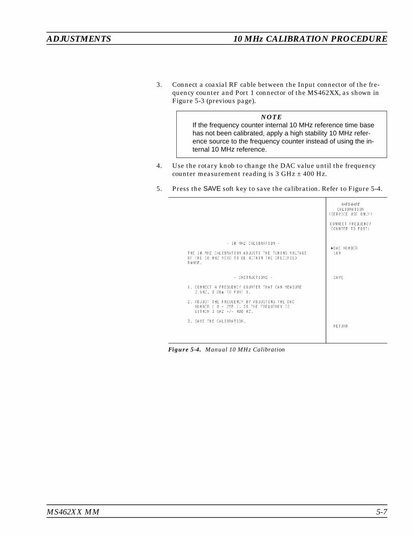
3. Connect a coaxial RF cable between the Input connector of the fre-quency counter and Port 1 connector of the MS462XX, as shown inFigure 5-3 (previous page).
NOTEIf the frequency counter internal 10 MHz reference time basehas not been calibrated, apply a high stability 10 MHz refer-ence source to the frequency counter instead of using the in-ternal 10 MHz reference.
4. Use the rotary knob to change the DAC value until the frequencycounter measurement reading is 3 GHz ± 400 Hz.
5. Press the SAVE soft key to save the calibration. Refer to Figure 5-4.
ADJUSTMENTS 10 MHz CALIBRATION PROCEDURE
MS462XX MM 5-7
Figure 5-4. Manual 10 MHz Calibration
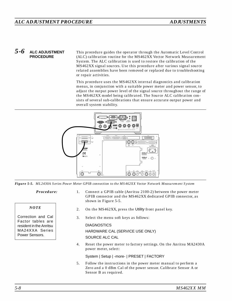
5-6 ALC ADJUSTMENTPROCEDURE
This procedure guides the operator through the Automatic Level Control(ALC) calibration routine for the MS462XX Vector Network MeasurementSystem. The ALC calibration is used to restore the calibration of theMS462XX signal sources. Use this procedure after various signal sourcerelated assemblies have been removed or replaced due to troubleshootingor repair activities.
This procedure uses the MS462XX internal diagnostics and calibrationmenus, in conjunction with a suitable power meter and power sensor, toadjust the output power level of the signal source throughout the range ofthe MS462XX model being calibrated. The Source ALC calibration con-sists of several sub-calibrations that ensure accurate output power andoverall system stability.
Procedure: 1. Connect a GPIB cable (Anritsu 2100-2) between the power meterGPIB connector and the MS462XX dedicated GPIB connector, asshown in Figure 5-5.
2. On the MS462XX, press the Utility front panel key.
3. Select the menu soft keys as follows:
DIAGNOSTICS
HARDWARE CAL (SERVICE USE ONLY)
SOURCE ALC CAL
4. Reset the power meter to factory settings. On the Anritsu MA2430Apower meter, select:
System | Setup | -more- | PRESET | FACTORY
5. Follow the instructions in the power meter manual to perform aZero and a 0 dBm Cal of the power sensor. Calibrate Sensor A orSensor B as required.
5-8 MS462XX MM
ALC ADJUSTMENT PROCEDURE ADJUSTMENTS
NOTE
Correction and CalFactor tables areresident in the AnritsuMA24XXA SeriesPower Sensors.
NoiseIn
Noise+28V
NO OPERATOR SERVICE-ABLE PARTS INSIDE.REFER SERVICING TOQUALIFIED PERSONNEL.
WARNING
CAUTIONFOR CONTINUED FIREPROTECTION REPLACEONLY WITH SPECIFIEDTYPE AND RATED FUSE.
IEEE 488.2GPIB
DedicatedGPIB
Serial Port Ethernet VGA SCSI-2
ExtAnalogOutput
ExtTrigger
LPT Line Printer Ext I/O
Port 1Port 2BiasBias
Port 2Bias Fuse
Port 1Bias Fuse
Ext AnalogIn
ExtSource
Ext 10 MHzIn
47-440 Hz85-264VAC
REPLACE FUSE ONLY WITHSAME TYPE AND RATING
CAUTIONDO NOT OPERATE
WITH POWER CORDUNGROUNDED
N274
00000001Made in UK
12-24V DC
(1.3A)
OUTPUT 1 OUTPUT 2 INPUT 1
DIGITAL
INPUT 2
ANALOG
CALIBRATORB
RS 232
PARALLEL PRINTER
GPIB / IEEE 488
CAUTIONDO NOT OPERATEWITH UNGROUNDEDPOWER CORD.
85-250 VAC
47-440Hz40VA MAX
SEE MANUAL FOR VOLTAGE RANGES ON BNC CONNECTORS
A
NO OPERATOR SERVICE-ABLE PARTS INSIDE.
WARNING
Figure 5-5. ML2430A Series Power Meter GPIB connection to the MS462XX Vector Network Measurement System

6. Press the menu soft key to select the source to be calibrated:
Select Source 1/2
7. Connect the power sensor to the selected port (Port 1 for Source 1,Port 3 for Source 2).
8. Select:
START CAL
9. After the ALC calibrations are complete, back up the calibrations byselecting SAVE TO HARD DISK.
If the calibration fails:
� Verify that the power meter and sensor are functioning correctly,the GPIB cables are in good condition, and all connections are se-cure.
� Note the failed step in the calibration procedure from the screenmessage.
� Repeat the calibration.If it still fails, proceed to Chapter 6—Troubleshooting.
ADJUSTMENTS ALC ADJUSTMENT PROCEDURE
MS462XX MM 5-9

5-7 BACK-ENDATTENUATORCALIBRATION(OPTION 4X ONLY)
The Back-end Attenuator calibration is used to characterize the attenu-ator in the Option Module for use in insertion gain calculations. Performthis procedure after the Option Module assembly has been removed orreplaced due to troubleshooting or repair activities.
This procedure uses the MS462XX internal diagnostics and calibrationmenus.
Procedure: 1. Allow the instrument to warm up for a period of at least 60 minutesfrom power on. If the power supply is interrupted for any reason, al-low a similar settling period.
2. On the MS462XX, press the Utility front panel key.
3. Select the menu soft keys as follows:
DIAGNOSTICS
HARDWARE CAL (SERVICE USE ONLY)
BACK-END ATTENUATOR CAL
4. Connect a throughline (Anritsu 3670 Series) between Port 1 andPort 2.
5. Select:
START CAL
5-10 MS462XX MM
BACK-END ATTENUATOR ADJUSTMENTS

5-8 NOISE SOURCESIGNAL INTERNALTHROUGH PATHCHARACTERIZATION(OPTION 4X ONLY)
This procedure provides steps for characterizing the Noise Source SignalInternal Through Path. A file known as the “Internal ENR Extension Ta-ble” will be created having the extension “EXT.”
Perform this procedure after the Port 1 Switch Module, Port 1 Module, as-sociated RF cables, connectors and/or rear panel Noise Source Input Con-nector have been replaced or disturbed due to troubleshooting or repairactivities. Also, perform this procedure after the CPU module has been re-placed.
EquipmentRequired:
The following equipment is required to perform this adjustment:
� Anritsu 37000 Series VNA or MS462XX Series VNMS� Anritsu 3750R or 3750LF Calibration Kit� Anritsu 3670K50-2 Throughline� Appropriate Adapters (Anritsu 34NK50, 34NFK50, 34AS50,
33LL50)
Procedure: 1. For MS462XX units with Option 4, 4D, or 4F, set up the 37000 VNAor MS462XX VNMS for a Start Frequency of 50 MHz, Stop Fre-quency of 3 GHz, and Data Points to 101. For MS462XX units withOption 4B, 4E, or 4G, set the Stop Frequency to 6 GHz and DataPoints to 201. Set up the test port connectors as follows: Port 1 for3.5 mm male and Port 2 for 3.5 mm female.
ADJUSTMENTS NOISE SOURCE
MS462XX MM 5-11
NOTE
The MS462XX VNMS mentioned above is not the same instrument thatis being tested in this procedure. This instrument is used to measure theMS462XX and is hereafter called the Measurement unit. The MS462XXunder test is hereafter called UUT.

2. Attach the throughline to both Port 1 and Port 2 of the Measure-ment unit (Figure 5-6).
3. Perform a 2-Port, 12-Term calibration on the Measurement unit.
4. After performing the calibration, connect Port 1 of the Measurementunit to Noise In on the rear panel of the UUT and Port 2 of the Mea-surement unit to Port 1 of the UUT. Use adapters as needed.
5. Press the Appl key on the front panel of the UUT.
6. Select:
CHANGE APPLICATION SETUP/MEASUREMENT TYPE
NOISE FIGURE
NOISE FIGURE SETUP
INTERNAL
7. Verify S12 and S21 on the Measurement unit are approximately�3 dB.
8. Set up all four channels on the Measurement unit for a Real &Imaginary graph type. Also, set up Ch 2 for S21 measurement andCh 3 for S12 measurement.
9. Save the data onto a floppy disk as a Text file (Print Output Device= Disk File). Name the file as follows: Nxxxxxx where xxxxxx is theserial number of the UUT. The operating software of the Measure-ment unit will automatically append the “.txt” extension to the filename.
5-12 MS462XX MM
NOISE SOURCE ADJUSTMENTS
Front
Rear
Port 1
Port 1
Port 2
Port 2
Noise In
Unit Under Test MeasurementUnit
Throughline Cable(Use appropriateadapters)
Figure 5-6. Throughline Cables

Hint: Press the Hard Copy key to access this output function if the Mea-surement unit is a MS462XX VNMS. Press the Menu key under the HardCopy group if the Measurement unit is a 37000 VNA.
NOTEThe MS462XX VNMS and the 37000 VNA save text fileswith the “Read-Only” attribute turned on. Use the File/Prop-erties feature of Windows Explorer to disable the“Read-Only” attribute.
10. Open the text file (nxxxxxx.txt) with the Notepad program (suppliedwith Microsoft Windows). Make sure the data is in the format andorder shown below:
� S11 (real & imaginary)� S21 (real & imaginary)� S12 (real & imaginary)� S22 (real & imaginary)
Then delete the header information and save it as a text file again.
11. Use Port 2 of the Measurement unit to measure the input match ofthe Noise Source to be used with the UUT.
Hint: Set up the Measurement unit for Single Channel display and mea-sure S22.
12. Save the S22 data onto a floppy disk. Name the file as follows: NS.
13. Using the Notepad text editor, open the text file (ns.txt), delete theheader information, and save it as a text file again.
14. Import the data contained in the Nxxxxxx.txt file into an Excelspreadsheet. Delete the entire first column that has the row number1, 2, 3, etc.
15. Add the real and imaginary columns of the match data of the noisesource from the ns.txt file to the last two columns of the spread-sheet. Refer to the example in Figure 5-7, following page.
16. Now select all the cells of the spreadsheet and format them from the“scientific” form to the “general” form with five decimal places.
17. Save the spreadsheet as a text file by typing the following file name:“Nxxxxxx.ext” where xxxxxx is the serial number of UUT. This is theNoise Figure Internal ENR Extension Table file.
NOTEThe quotation marks are required in Excel for saving a filewith a specific filename.
ADJUSTMENTS NOISE SOURCE
MS462XX MM 5-13
NOTE
No bias is applied tothe noise source andthe S22 data must bein real and imaginaryformat.

18. Copy this file to a floppy diskette.
19. Insert the floppy diskette into the UUT floppy disk drive.
20. Press the Appl key and then select the following:
CHANGE APPLICATION SETUP
NOISE FIGURE SETUP
LOAD ENR TABLEFROM FLOPPY DISK
INTERNAL ENR EXTENSION TABLE
RETURN
21. Save the Internal ENR Extension table to hard disk: select the fol-lowing:
SAVE ENR TABLESTO HARD DISK
INTERNAL ENR EXTENSION TABLE
RETURN
5-14 MS462XX MM
NOISE SOURCE ADJUSTMENTS
Figure 5-7. Match Data Example

Table of Contents
6-1 INTRODUCTION . . . . . . . . . . . . . . . . . . . . . . . . . . . . . . . . . . . 6-3
6-2 SELF TEST . . . . . . . . . . . . . . . . . . . . . . . . . . . . . . . . . . . . . . 6-3
6-3 TROUBLESHOOTING TOOLS FOR THE CPU MODULE . . . . . . . . . . . . . 6-4SRAM . . . . . . . . . . . . . . . . . . . . . . . . . . . . . . . . . . . . . . . 6-6SRAM DISK . . . . . . . . . . . . . . . . . . . . . . . . . . . . . . . . . . . . 6-6FLASH MEMORY . . . . . . . . . . . . . . . . . . . . . . . . . . . . . . . . . 6-6EXTENDED FLASH MEMORY . . . . . . . . . . . . . . . . . . . . . . . . . 6-6DRAM . . . . . . . . . . . . . . . . . . . . . . . . . . . . . . . . . . . . . . . 6-7GRAPHICS VRAM . . . . . . . . . . . . . . . . . . . . . . . . . . . . . . . . 6-7GRAPHICS DRAM . . . . . . . . . . . . . . . . . . . . . . . . . . . . . . . . 6-7DSP SRAM. . . . . . . . . . . . . . . . . . . . . . . . . . . . . . . . . . . . . 6-7
6-4 HARDWARE TROUBLESHOOTING. . . . . . . . . . . . . . . . . . . . . . . . . 6-8CPU MODULE . . . . . . . . . . . . . . . . . . . . . . . . . . . . . . . . . . 6-8SOURCE MODULE . . . . . . . . . . . . . . . . . . . . . . . . . . . . . . . . 6-9HET OSCILLATOR VOLTAGE . . . . . . . . . . . . . . . . . . . . . . . . . 6-11SOURCE 1 . . . . . . . . . . . . . . . . . . . . . . . . . . . . . . . . . . . . 6-12SOURCE 2 . . . . . . . . . . . . . . . . . . . . . . . . . . . . . . . . . . . . 6-12LO . . . . . . . . . . . . . . . . . . . . . . . . . . . . . . . . . . . . . . . . . 6-12AUTO LEVEL CONTROL (ALC) . . . . . . . . . . . . . . . . . . . . . . . . 6-13RECEIVER MODULE . . . . . . . . . . . . . . . . . . . . . . . . . . . . . . 6-16NOISE SOURCE POWER SUPPLY. . . . . . . . . . . . . . . . . . . . . . . 6-21POWER DISTRIBUTION UNIT. . . . . . . . . . . . . . . . . . . . . . . . . 6-21FRONT PANEL ASSEMBLY . . . . . . . . . . . . . . . . . . . . . . . . . . 6-22
6-5 SOFTWARE PROBLEM . . . . . . . . . . . . . . . . . . . . . . . . . . . . . . . 6-23
6-6 MEASUREMENT QUALITY PROBLEM . . . . . . . . . . . . . . . . . . . . . . 6-23
6-7 NOISE FIGURE MEASUREMENT PROBLEM . . . . . . . . . . . . . . . . . . 6-24
6-8 FREQUENCY TRANSLATING GROUP DELAY MEASUREMENT . . . . . . . 6-27
Chapter 6Troubleshooting


Chapter 6Troubleshooting
6-1 INTRODUCTION It is strongly recommend that any MS462XX Vector Network Measure-ment System repair be performed by qualified technical personnel only.
Refer to Section 1-8 for a listing of spare parts mentioned in this chapter.Contact your nearest Anritsu Customer Service or Sales Center for priceand availability information. See Chapter 7 for specific module removaland replacement instructions. Refer to the MS462XX Vector NetworkMeasurement System Operation Manual (10410-00203) for the specific op-erating instructions referred to in these procedures.
This chapter provides procedures to accurately define and isolate thefault to a specific assembly or module.
An aide to troubleshooting instrument failures is a good understanding ofthe system and subassembly operation. Refer to the descriptions of sys-tem and subassembly operations and block diagrams located inChapter 2—Theory of Operation.
Accurately defining a fault is the most important step in troubleshootingan instrument. The fault symptoms should be noted by performing afunctional test on the system, as explained in Chapter 3—OperationalPerformance Tests.
Faults can be categorized as the following:
� Hardware problems� Software problems� Measurement problems
6-2 SELF TEST The VNMS has two self tests:
� Short self test at initial bootup� Extended self test within the Diagnostics menu.
Both self tests display either Pass or Fail on the VNMS display upon com-pletion Each self test failure will add the appropriate failure informationto the Service Log.
The short self test at bootup performs the following tests:
� Communication with the Source(s), Options board, and ReceiverBoard
� CPU power supply voltage regulation� Test of CPU lithium battery (found only on BMS software version
1.16 and above)
MS462XX MM 6-3
CAUTION
The procedures in thischapter should beperformed by qualifiedtechnical personnelonly. These proceduresmay require access tointernal components,and care should betaken to avoid contactwith potent ia l lyhazardous voltages.

The extended self test is initiated by pressing the Utility key, then select-ing:
Diagnostics
Start Self Test
The extended self test performs extensive tests on the entire instrument,but the RF signal paths and components are minimally tested. Only theDown Converter Module and the Receiver PCB 125KHz IF signal pathsare tested during the extended self test.
6-3 TROUBLESHOOTINGTOOLS FOR THE CPUMODULE
The MS462XX Vector Network Measurement System has built-in diag-nostic tools to aid in troubleshooting the CPU Module. They are accessedfrom the Utility key in the enhancement key group on the front panel.
Entering theTroubleshooting
Menu
1. On the MS462XX Vector Network Measurement System, press theUtility front panel key.
2. Select the menu soft keys as follows:
DIAGNOSTICS
TROUBLESHOOTING
MORE
MORE
Exiting theTroubleshooting
Menu
The MS462XX Vector Network Measurement System must be properlyexited from the Troubleshooting function in order to restore normal sys-tem operation. To exit the troubleshooting menu:
1. Select the menu soft keys as follows:
FINISHED, RECOVER FROM TROUBLESHOOTING
2. If the system still does not function properly, select the menu softkeys as follows:
UTILITY
DIAGNOSTICS
TROUBLESHOOTING
FINISHED, RECOVER FROM TROUBLESHOOTING
6-4 MS462XX MM
CPU MODULE TROUBLESHOOTING

TheTroubleshooting
Menu
The Troubleshooting menu is shown in the graphic screen capture below.Descriptions of the menu selections follow.
MS462XX MM 6-5
TROUBLESHOOTING CPU MODULE
Figure 6-1. Troubleshooting Menu

SRAM This test verifies whether the internal SRAM is functioning properly. Ifthis test fails, the instrument beeps and the Front Panel LEDs flash. Theinstrument will automatically reboot after this test is complete.
SRAM DISK This test verifies whether the internal SRAM disk is functioning properly.The SRAM disk is also known as the hard disk when no external harddisk is connected to the SCSI-2 port. If the test fails, the instrument willbeep and the Front Panel LEDs will flash.
To reformat the SRAM disk:
1. Press the Utility front panel key.
2. Select the menu soft keys as follows:
GENERAL DISK UTILITIES
FORMAT HARD DISK
FLASH MEMORY This test verifies whether the internal Flash Memory is functioning prop-erly.
EXTENDED FLASHMEMORY
This test verifies whether the internal Extended Flash Memory is func-tioning properly.
6-6 MS462XX MM
CPU MODULE TROUBLESHOOTING
CAUTION
The SRAM disk test overwrites the Harmonic Cal coefficients and all the con-tents of the SRAM disk. The SRAM disk must be reformatted after the test iscomplete.
CAUTION
This test overwrites the instrument control software. Basic Measurement Soft-ware must be re-loaded from floppy diskette after this test is complete and theinstrument is turned off.
CAUTION
The SRAM test overwrites all front panel setups (including internal), Cal coef-ficients and the Service Log.
CAUTION
This test overwrites the instrument control software. Basic Measurement Soft-ware must be re-loaded from floppy diskette after this test is complete and theinstrument is turned off.
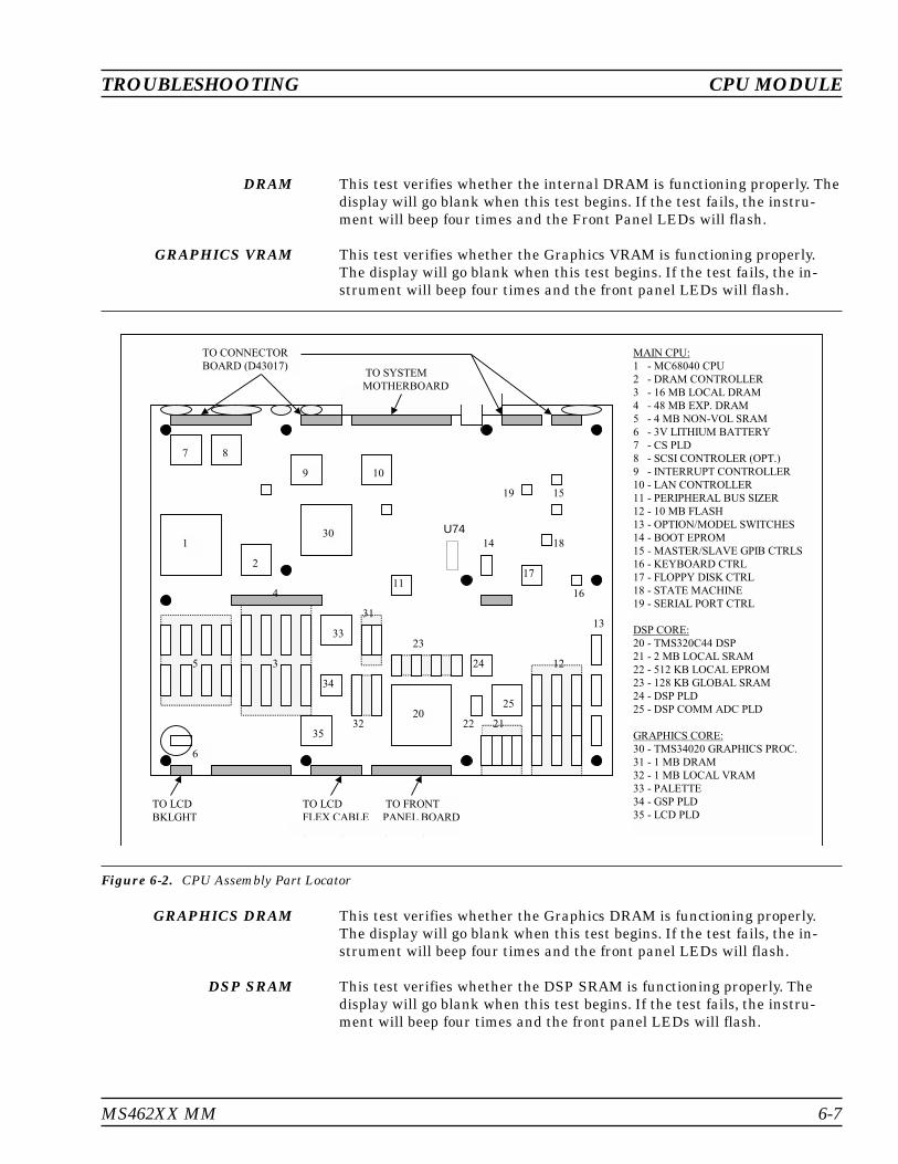
DRAM This test verifies whether the internal DRAM is functioning properly. Thedisplay will go blank when this test begins. If the test fails, the instru-ment will beep four times and the Front Panel LEDs will flash.
GRAPHICS VRAM This test verifies whether the Graphics VRAM is functioning properly.The display will go blank when this test begins. If the test fails, the in-strument will beep four times and the front panel LEDs will flash.
GRAPHICS DRAM This test verifies whether the Graphics DRAM is functioning properly.The display will go blank when this test begins. If the test fails, the in-strument will beep four times and the front panel LEDs will flash.
DSP SRAM This test verifies whether the DSP SRAM is functioning properly. Thedisplay will go blank when this test begins. If the test fails, the instru-ment will beep four times and the front panel LEDs will flash.
TROUBLESHOOTING CPU MODULE
MS462XX MM 6-7
24
25
22
13
11
109
87
6
5 3
1
2
TO FRONT
PANEL BOARD
(D43018)
MAIN CPU:
1 - MC68040 CPU
2 - DRAM CONTROLLER
3 - 16 MB LOCAL DRAM
4 - 48 MB EXP. DRAM
5 - 4 MB NON-VOL SRAM
6 - 3V LITHIUM BATTERY
7 - CS PLD
8 - SCSI CONTROLER (OPT.)
9 - INTERRUPT CONTROLLER
10 - LAN CONTROLLER
11 - PERIPHERAL BUS SIZER
12 - 10 MB FLASH
13 - OPTION/MODEL SWITCHES
14 - BOOT EPROM
15 - MASTER/SLAVE GPIB CTRLS
16 - KEYBOARD CTRL
17 - FLOPPY DISK CTRL
18 - STATE MACHINE
19 - SERIAL PORT CTRL
DSP CORE:
20 - TMS320C44 DSP
21 - 2 MB LOCAL SRAM
22 - 512 KB LOCAL EPROM
23 - 128 KB GLOBAL SRAM
24 - DSP PLD
25 - DSP COMM ADC PLD
GRAPHICS CORE:
30 - TMS34020 GRAPHICS PROC.
31 - 1 MB DRAM
32 - 1 MB LOCAL VRAM
33 - PALETTE
34 - GSP PLD
35 - LCD PLD
4
20
30
12
21
23
31
32
33
34
35
14
15
16
17
18
19
TO LCD
BKLGHT
TO LCD
FLEX CABLE
(D43020)
TO SYSTEM
MOTHERBOARD
TO CONNECTOR
BOARD (D43017)
Figure 6-2. CPU Assembly Part Locator
U74
6-4 HARDWARETROUBLESHOOTING
The Scorpion Vector Network Measurement System hardware includesthe following:
� CPU Module� Source Module(s)� Receiver Module� Power Supply (PDU) Module� Front Panel Assembly� Option Module (for units equipped with Option 4 or 5 only)
CPU MODULE CPU module-related system failures include:
� System does not boot up� Display problems� Printer Problems� GPIB Interface Problems
System Boot-upProblem
This condition can be a result of a failure of the +6.5 volt output of thePower Distribution Unit, failure of the CPU module memory, or a dis-lodged Lithium Battery mounted on U74 (next to the boot EPROM).
1. Verify that the +6.5 volt output of the Power Distribution Unit isworking properly.
2. Verify that the battery mounted on U74 is installed properly. Referto Figure 6-2 on the previous page for a part location diagram.
3. Replace the CPU Module.
Hard DiskProblem
This condition can be a result of a failure of the Lithium Battery or CPUmodule.
1. Replace the Lithium Battery (p/n: 633-25) on the CPU as describedin Chapter 7 (Removal and Replacement Procedures), page 7-15.
2. If the problem persists, replace the CPU assembly.
6-8 MS462XX MM
HARDWARE TROUBLESHOOTING TROUBLESHOOTING

Printer OutputProblem
This condition can be a result of a failure of the printer, printer cable, orCPU module.
1. Connect a different printer and determine if the instrument workswith that printer. If so, replace the printer.
2. Replace the printer cable.
3. Replace the CPU module.
GPIB InterfaceProblem
This condition can be a result of a failure of the CPU module.
1. Connect a GPIB cable between the IEEE488 port and the DedicatedGPIB port on the rear panel.
2. Press the Utility front panel key.
3. Select the menu soft keys as follows:
DIAGNOSTICS
PERIPHERAL TESTS
GPIB INTERFACE
4. Follow the instructions on the screen until the test is completed.
5. If the GPIB Interface test fails, replace the CPU Module.
GPIB AddressRetention
Problem
This condition can be a result of a failure of the Lithium Battery.
Replace the Lithium Battery (p/n: 633-25) on the CPU as described onpage 7-15.
SOURCE MODULE Possible Source Module related system failures include:
� Phase-lock loop failures� ALC failures� Insufficient dynamic range� Excessive high level noise� Excessive harmonics� Slow sweep speed
TROUBLESHOOTING HARDWARE TROUBLESHOOTING
MS462XX MM 6-9
CAUTION
Ensure that no other GPIB cables are connected to either of the two rearpanel GPIB connectors when performing this test.

Phase-lock LoopProblem
If the MS462XX detects a Phase-lock loop problem during normal opera-tion, an error code followed by a brief error message will be displayed onthe screen. The error code will also be written to the service log alongwith some of the operating data gathered from the system at the time offailure. Possible causes include:
� 10 MHz Reference Signal missing� Internal VCO of Source Module failure� Faulty communication to the Source Module� Power Supply failure
Troubleshooting tools include:
� Service Log: Error codes are written to the service log along withdata representing system conditions at the time of failure.
� Phase-lock Error Codes: Phase-lock error codes have an alphabet-ical suffix (code) following the message. This suffix code consistsof one or more letters from A to F or from J to L that representthe portion of the source circuits that were not locked. ThePhase-lock failure mode suffix codes are listed in the table below:
Suffix Failure Mode
A Source 1 DDS Clock Lock Fail
B HET Lock Fail
C LO Offset Lock Fail
D Source 1 Offset Lock Fail
E LO Main Lock Fail
F Source 1 Main Lock Fail
J Source 2 DDS Clock Lock Fail
K Source 2 Offset Lock Fail
L Source 2 Main Lock Fail
Depending on the nature of the failures and the frequency band when thefailure occurred, more than one failure suffix may be displayed. Suffixesdo not necessarily appear in alphabetical order.
Examples:
6100 PHS LCK FAIL FCBALJ
6100 PHS LCK FAIL CBALJ
Both example error messages were caused by the absence of the 10 MHzReference Time Base Signal. The first message occurred when the instru-ment was sweeping from 820 MHz to 850 MHz. The second message oc-curred when the instrument was sweeping from 10 MHz to 6 GHz.
6-10 MS462XX MM
HARDWARE TROUBLESHOOTING TROUBLESHOOTING

HET OSCILLATORVOLTAGE
This function (Figure 6-3) allows the user to verify whether the HET os-cillator of the Main Source Module is operating properly.
TROUBLESHOOTING HARDWARE TROUBLESHOOTING
MS462XX MM 6-11
Figure 6-3. Source Module Troubleshooting Menu

SOURCE 1 This function allows the user to verify that various parts of the mainSource Module are operating properly, and includes the following tests:
DDS REFERENCE CLOCK VOLTAGE
OFFSET VCO VOLTAGE
MAIN VCO VOLTAGE
LEVEL AMPLIFIER VOLTAGE
LOG AMPLIFIER VOLTAGE
POWER LEVEL DAC VOLTAGE
ALC MODULATOR DRIVE VOLTAGE
SOURCE 2 This function allows the user to verify that the Option Source Module isoperating properly. This function includes the following tests:
DDS REFERENCE CLOCK VOLTAGE
OFFSET VCO VOLTAGE
MAIN VCO VOLTAGE
LEVEL AMPLIFIER VOLTAGE
LOG AMPLIFIER VOLTAGE
POWER LEVEL DAC VOLTAGE
ALC MODULATOR DRIVE VOLTAGE
LO This function allows the user to verify whether the Local Oscillator is op-erating properly, and includes the following tests:
OFFSET VCO VOLTAGE
MAIN VCO VOLTAGE
Check the Service Log and use the error code suffix table to determinethe area where the source module is having the problem.
1. Press the Utility front panel key.
6-12 MS462XX MM
HARDWARE TROUBLESHOOTING TROUBLESHOOTING
NOTECommon Offset Mode must be turned off for the OFFSET VCO VOLT-AGE function to operate properly. To turn common offset mode off, se-lect RETURN/SELECT MODES/COMMON OFFSET MODE OFF.
NOTECommon Offset Mode must be turned off for the OFFSET VCO VOLT-AGE function to operate properly. To turn common offset mode off, se-lect RETURN/SELECT MODES/COMMON OFFSET MODE OFF.

2. Select the menu soft keys as follows:
DIAGNOSTICS
SERVICE LOG
3. Check the Power Distribution Unit output voltage.
4. Use a frequency counter or Spectrum Analyzer to verify whether avalid 10 MHz signal is being received at J2 of both the Main SourceModule and the Option Module.
5. If the 10 MHz signal is missing, verify whether the instrument is setup to use an external 10 MHz reference.
6. Press the Utility front panel key.
7. Select the menu soft keys as follows:
REAR PANEL
8. Assure that the INTERNAL setting is selected for REFERENCEFREQUENCY.
9. Use the built-in diagnostic tests to verify whether the source moduleis operating properly. If the test results indicate an out of limit con-dition, replace the appropriate source module.
AUTO LEVELCONTROL (ALC)
If the MS462XX detects an ALC problem during normal operation, an errormessage will be displayed on the screen. The error code will also be written tothe service log along with some of the operating data gathered from the sys-tem at the time of failure.
Possible causes of ALC failure include:
� Insufficient static protection at the VNMS Test Ports� Not enough power out of the source module� Insufficient ALC modulation depth� Broken path to or from the ALC detector� Broken path to the instrument port modules� Improper switching within components
(including the Source Module)� Defective ALC detector diode in the Non-Reversing Module,
Auto-Reversing Module, or Port 3 Module� Path to/from the ALC detector is broken� Path to the instrument port modules is broken� Source Module failed
MS462XX MM 6-13
TROUBLESHOOTING HARDWARE TROUBLESHOOTING

Troubleshooting tools include:
� Service Log: Error codes will be written to the service log alongwith some data representing system conditions at the time offailure.
ALC Error Codes:
ALC1 LVLD FAIL Source 1 ALC Leveled Failure
ALC2 LVLD FAIL Source 2 ALC Leveled Failure
� ML243XA Power Meter� MA247XA Power Sensor
The presence of these error codes do not necessarily indicate an instru-ment failure. They simply indicate that an RF unleveled condition existedunder a specific condition. For example, when the RF output level is set toa value exceeding the maximum power output range, the instrument willdisplay these error codes. However, they do indicate that a failure condi-tion does exist if the RF output level is within the power output range ofthe instrument.
It is useful to verify the ALC calibration as follows:
1. Connect the GPIB port of the Power Meter to the Dedicated GPIBport of the MS462XX and perform a new ALC calibration.
2. Press the Utility front panel key.
3. Select the menu soft keys as follows:
DIAGNOSTICS
HARDWARE CAL
SOURCE ALC CALIBRATION
4. Check the source module cabling and the cabling to the componentson the Receiver Module.
5. Use the a1/1 user defined measurement mode to compare the leveledport power level (0 dBm) and the unleveled port power (+20 dBm).
6. Press the Power front panel key.
7. Select the menu soft keys as follows:
SOURCE 1 SETUP
SOURCE 1 POWER
6-14 MS462XX MM
HARDWARE TROUBLESHOOTING TROUBLESHOOTING

A typical profile of unleveled power is shown in Figure 6-4. If the leveledtrace looks like the unleveled trace, it indicates that a problem has oc-curred in the ALC circuitry. Replace the source module, Non-ReversingModule (MS462XA only), Auto -Reversing Module (MS462XB only), orPort 3 Module (MS462XB with Option 3A or 3B only).
TROUBLESHOOTING HARDWARE TROUBLESHOOTING
MS462XX MM 6-15
Figure 6-4. Typical Profile of Unleveled Power

RECEIVERMODULE
There are four receiver module related system failures:
� 10 MHz Reference Oscillator failures� ALC failures� RF Component failures� Noise Source Power Supply failures
Special fixtures consists of the items listed below:
Part Number Description Quantity
D43023-3 Flex Extender PCB Assembly 1
806-89 3- foot flex coax cable 3
49523 2-foot MCX to MCX cable 4
The use of these special fixtures allows the Receiver Module be placed ontop of the instrument, which provides easy access to component assem-blies for troubleshooting (see Figures 6-5 and 6-6).
6-16 MS462XX MM
HARDWARE TROUBLESHOOTING TROUBLESHOOTING
NOTE
When the Receiver Module is placed on top of the instrument, use:
• 806-89 coax cables to replace the semi-rigid RF cables connected between theSource Modules and the RF components in the Receiver Module
• 49523 cables to replace the four MCX cables connecting between the ReceiverPCB Assembly and the Source Modules

TROUBLESHOOTING HARDWARE TROUBLESHOOTING
MS462XX MM 6-17
Figure 6-5. Rear Panel Showing Receiver Module Placed for Easy Access
Receiver Module
Figure 6-6. Receiver Module Connected using Flexible Cable
Flexible Cable

10 MHz ReferenceOscillator
Problem
Possible causes are listed below:
� 10 MHz Reference Oscillator failure� Power Supply failure
Troubleshooting tools include:
� Service Log: Since the 10 MHz reference plays an important rolein every phase lock circuitry in the instrument, an error messagedisplayed on the screen may include a series of suffixes indicat-ing various phase lock loop failures.
Error Code Examples:
100 PHS LCK FAIL FCBALJ
6100 PHS LCK FAIL CBALJ
Both error messages are caused by the 10 MHz Reference Time BaseSignal not being present. The first message occurs when the instrumentis sweeping from 820 to 850 MHz. The second message occurs when theinstrument is sweeping from 10 MHz to 6 GHz.
1. Check the Service Log. Press the Utility key and select:
DIAGNOSTICS
SERVICE LOG
If there are multiple suffix codes, the problem may be caused by the10 MHz Reference Oscillator.
2. Check the Power Distribution Unit output voltage.
3. Use a frequency counter or Spectrum Analyzer to verify whether avalid 10 MHz signal is received at J2 of both the Main Source Mod-ule and the Option Module.
4. If the 10 MHz signal is missing, verify that the instrument is set upto use an external 10 MHz reference. Press the Utility key and se-lect:
REAR PANEL (left)
Assure that the INTERNAL setting is used for the REFERENCEFREQUENCY.
5. If the 10 MHz signal is not present, replace the Receiver PCB As-sembly.
6-18 MS462XX MM
HARDWARE TROUBLESHOOTING TROUBLESHOOTING
RETURN
INTERNAL / EXTERNAL
FREQUENCY
REFERENCE
DRIVEN PORT
TTL OUTPUT
VERTICAL
HORIZONTAL
(XXX)
SELECT OUTPUT MODE
VOLTAGE
OUTPUT ON / OFF
REAR PANEL

Figure 6-7 shows the RF components layout in the Receiver Module. Fig-ure 6-8 shows the system cabling.
TROUBLESHOOTING HARDWARE TROUBLESHOOTING
MS462XX MM 6-19
10 MHz
X2
X2IF
IF
PREAMP
ARM
STEPATTN
STEPATTN
NFIG
NFIG
P2P1
P3
DOWNCONVERSIONMODULE
Figure 6-7. RF Components Layout in Receiver Module
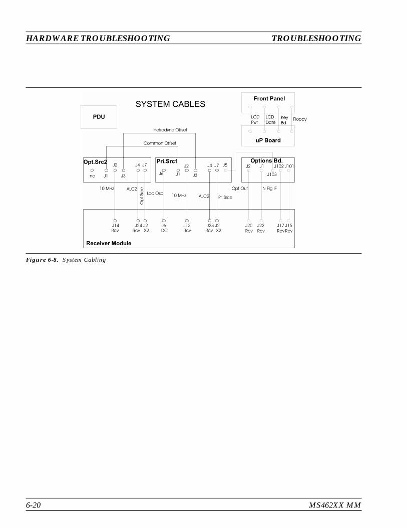
6-20 MS462XX MM
HARDWARE TROUBLESHOOTING TROUBLESHOOTING
Pri.Src1Opt.Src2
Receiver Module
Options Bd.
Front Panel
uP Board
PDU
SYSTEM CABLES
Hetrodyne Offset
Common Offset
nc J1
J2
J3
J4 J7
10 MHz
10 MHz
ALC2
ALC2
Op
tSr
ce
Loc OscPri Srce
Opt Out N Fig IF
J6 J1
J1J2 J2
J3
J4 J7 J5
LCD
Pwr
LCD
DateKey
BdFloppy
J14 J24 J2 J6 J13 J23 J2 J20
Rcv
J22
RcvRcv RcvRcvRcv X2 X2DCJ15
Rcv
J17
Rcv
J101J102
J103
Figure 6-8. System Cabling

NOISE SOURCEPOWER SUPPLY
The following steps can help isolate noise source power supply failures:
1. Use an oscilloscope to measure the Noise Source power supply out-put. Connect the probe to the rear panel BNC connector marked“Noise +28 V.”
2. Press the Appl key and select the following soft keys:
CHANGE APPLICATION SETUP
MEASUREMENT TYPE
NOISE FIGURE
3. Observe that a pulsed +28 V DC signal appears on the Oscilloscope.If not present, replace the Receiver PCB assembly.
POWERDISTRIBUTION
UNIT
A procedure for troubleshooting the Power Distribution Unit is given be-low.
The following steps can help isolate power distribution unit failures:
1. Turn the MS462XX off and disconnect the power cord.
2. Remove the Backplane cover (Figure 7-15, page 7-23).
3. Reconnect the power cord and turn the MS462XX on.
4. Use a DMM to measure the power supply output voltages listed inFigure 6-9 at the Back Plane PCB Assembly (refer to Figure 7-16,page 7-24).
5. If any of the DC voltage tests fail, replace the Power DistributionUnit.
TROUBLESHOOTING HARDWARE TROUBLESHOOTING
MS462XX MM 6-21
NOTE
All vol tages arereferenced to groundexcept 5V Float and5V Float Returnterminals that shouldhave 5 volt potentialbetween them.
13 1
1425
Figure 6-9. Backplane Connector Pinout
Voltage Pins Common Pins
+15�3% 7 & 19 Ground 6 & 18
�15�3% 9 & 21 Ground 8 & 20
+6.5�2% 13 & 25 Ground 12 & 24
+28�3% 14 Ground 12 & 24

FRONT PANELASSEMBLY
There are three Front Panel Assembly related failures:
� Non responsive keys� Non responsive front panel knob� LCD Display problems
Front PanelKeys/Knobs
Problem
The following could cause non-responsiveness:
� Defective keypad� Corroded key traces on front panel PCB assembly� Defective front panel knob encoder
To troubleshoot a front panel key or knob problem, use the following pro-cedure:
1. Press the Utility key and select the following soft keys:
DIAGNOSTICS
PERIPHERAL TESTS
FRONT PANEL
2. Follow the instructions on the LCD screen until the test is com-pleted.
3. If the test fails, replace the front panel PCB assembly and keypad.
LCD Problems To troubleshoot an LCD problem, use the following procedure:
1. Connect an external VGA monitor to the rear panel. If no dislay ap-pears on the VGA display, check the PDU output voltages (see previ-ous page). If the voltages are OK, replace the CPU assembly.
2. If the external VGA display is OK, the following assemblies mayhave failed and in need of replacement:
� Backlight Lamp (replaceable on Sharp model LQ9D340 only)� Backlight Driver PCB� LCD Display (only Anritsu part number 15-100 is available)� CPU Assembly
Floppy DriveRead/Write
Problems
The floppy disk drive is not serviceable. If the unit fails to read or writedata, the disk drive head may need cleaning. Any standard floppy diskdrive cleaning kit may be used to clean the disk drive head. Follow themanufacturer’s instructions for using the cleaning kit.
6-22 MS462XX MM
HARDWARE TROUBLESHOOTING TROUBLESHOOTING
Hint
If the image on theLCD display is upsidedown, disconnectand then reconnectthe LCD flex cable.This should correctthe problem.

6-5 SOFTWAREPROBLEM
It is important to provide the factory as many details of the conditionsimmediately preceding the onset of the problem. This important informa-tion can provide clues and aid the factory in reproducing the problem.When encountering a software problem, please note the following:
� Measurement mode (S-parameters, noise figure, etc.)� Frequency range� Source 1 power level setting� Source 2 power level setting, if applicable� Number of data points used� Number of channels displayed� Type of graph type displayed� Sequence of key presses preceding the onset of problem, if appli-
cable� Data plots showing the problem
Please provide the above information to the Service Support Engineerwhen contacting the factory.
6-6 MEASUREMENTQUALITYPROBLEM
If the MS462XX measurement quality is suspect, the following para-graphs provide guidelines and hints for determining possible measure-ment quality problems.
The quality of the MS462XX measurements is determined by the follow-ing test conditions and variables:
� Condition of the MS462XX� Quality and condition of the interface connections and connectors� Quality and condition of the calibration components,
throughlines, adapters, and fixtures� Surrounding environmental conditions at the time of the
measurement� Selection and performance of the calibration for the DUT being
measured
MeasurementConditions Check
When determining possible measurement problems, check the DUT andthe calibration conditions:
1. Ensure that the proper calibration was accomplished for the devicebeing measured.
For high insertion loss device measurements, the calibration shouldinclude isolation, high number of averages and lower IF Bandwidthsetting during calibration.
For low-loss device measurements, the calibration should also in-clude a sliding load calibration, if possible.
TROUBLESHOOTING SOFTWARE PROBLEM
MS462XX MM 6-23

2. Check DUT mating connector(s) condition and pin depth.
3. Measure an alternate known good DUT, if possible.
4. Check if the environment is stable enough for the accuracy requiredfor the DUT measurement.
5. Check that the system has not been subjected togreater-than-specification variations in temperature.
6. Check that the system has not been placed in direct sun light ornext to a changing cooling source, such as a fan or air conditioningunit.
7. Check the calibration using known good components from the cali-bration kit. If measurements of these devices do not produce good re-sults, perform Steps 8 and 9.
8. Check the throughline cable stability, including condition and pindepth. Replace with a known good cable, if necessary.
9. Check the condition and pin depth of the calibration kit components.Replace them with known good components, if necessary.
10. Check the system performance as follows:
� Perform the Signal Path Tests that are part of the OperationalTest.
� Perform the Performance Verification Test.
6-7 NOISE FIGUREMEASUREMENTPROBLEM
This section describes some commonly encountered noise figure measure-ment problems and their solutions.
Problem The NOT ALLOWED error message is displayed when selecting NOISEFIGURE WITH 12 TERM under the PERFORM CAL menu:
Solution Perform a new 12-term S-parameter calibration between 50 MHz and6 GHz (50 MHz and 3 GHz with Option 4).
Noise Figure is only available between 50 MHz and 6 GHz. S-parametercalibrations outside this frequency range generates the NOT ALLOWEDerror message.
Problem Negative Noise Figure:
Solution Use the same Source Power setting in both the Transmission/Reflectionand Noise Figure setup.
6-24 MS462XX MM
NOISE FIGURE MEASUREMENT PROBLEM TROUBLESHOOTING
Account for a calibration performed with loss and later removed for themeasurement.
Problem NOISE FIGURE OVERLOAD error message displayed:
Solution DUT has too much gain (typically >30 dB). Use an attenuator to reducethe input power to Port 2.
Try using a 5 dB ENR Noise Source.
Problem Significant difference between Internal and External Noise Source mea-surement:
Solution 1. Check for the presence of the Internal ENR Extension Table file(Nxxxxx.EXT).
2. Check the Nxxxxxx.nfx External ENR Extension Table file if addi-tional length is inserted between Port 1 (Internal ENR ExtensionTable reference plane) and DUT.
3. If the External ENR Extension Table does not exist, it can be gener-ated internally by measuring the S-parameters of the extension ca-ble, creating a “s2p” file and then changing the file extension to “nfx”by using an external Personal Computer.
Problem Noise Figure response contains irregular discontinuities:
Solution Try the Narrow Bandwidth Measurement Mode.
Perform a Back-end Attenuator calibration (refer to Chapter 5).
NOTEThe irregularity may be caused by contamination (other signals) in theenvironment and the spurious response of the DUT.
Problem Noise Figure response contains too many ripples:
Solution Turn Noise Figure Averaging on.
Try using a 15 dB ENR Noise Source.
NOTEThe problem may be caused by the very poor matches of DUT or apassive DUT. The second stage calculations are less accurate whenmeasuring Noise Figure for a passive device.
Problem Fails the Noise Figure Assurance Check:
Solution Perform a Back-end Attenuator calibration (refer to Chapter 5).
Replace the Option Module.
TROUBLESHOOTING NOISE FIGURE MEASUREMENT PROBLEM
MS462XX MM 6-25

Problem Fails the Raw Receiver Noise Figure Check:
Solution Check the setup connections:
1. Check the Noise Source ENR Table stored on the instrument. Referto the MS462XX Scorpion Measurement Guide (P/N: 10410-00213)for instructions on how to create a new ENR Table file.
2. Check the Internal ENR Extension Table stored on the instrument.Refer to Chapter 5, Section 5-8 of this manual, for instructions onhow to create a new Internal ENR Extension Table file.
3. If the instrument fails this test in Wideband External Noise SourceMode, but passes the Noise Figure Assurance Test, try anotherNoise Source.
NOTEA new Noise Source Vendor ENR Table must be loaded into the instru-ment prior to using a new noise source.
4. If the instrument fails this test in Wideband Internal Noise SourceMode, but passes the test in External Noise Source Mode and the In-ternal ENR Extension Table is okay, replace the Port 1 Switch Mod-ule.
Problem Fails the Noise Figure Measurement Confidence Check:
Solution Perform a Back-end Attenuator calibration (refer to Chapter 5).
Replace the Option Module.
Problem Others:
Solution Consult the factory.
When consulting the factory with Noise Figure Measurement problems,please provide the following:
� S-parameter data� Noise Figure and Gain data� Y-Factor data� Sketch of a block diagram of the test setup� DUT specifications� Scorpion instrument settings:
Transmission/Reflection—Frequency, Source Power, IFBW, andAveragingNoise Figure—Frequency, DUT Bandwidth, Noise Source Loca-tion, Source Power, Noise Figure Averaging
6-26 MS462XX MM
NOISE FIGURE MEASUREMENT PROBLEM TROUBLESHOOTING

6-8 FREQUENCYTRANSLATINGGROUP DELAYMEASUREMENT
The measurement process consists of generating the modulating signal,modulating the source, demodulating the received signal, and performingthe phase comparison. The modulating signal is generated in the OptionModule and is fixed at 453.125 kHz. The modulating signal is input to J5of the Source Module 1 to modulate the source signal.
The demodulating of the received signal is done in the Option Module.
The phase comparison is done in the DSP section of the Receiver PCB.
If the instrument fails the Frequency Translating Group Delay test, re-place the assemblies in the following order:
1. Option Module
2. Source Module 1
3. Receiver PCB
NOTEThe Option Module is also used to perform a Noise FigureMeasurement. Perform a Noise Figure Measurement calibra-tion and operational check if the Option Module is replaced.
TROUBLESHOOTING GROUP DELAY
MS462XX MM 6-27/6-28


Table of Contents
7-1 INTRODUCTION . . . . . . . . . . . . . . . . . . . . . . . . . . . . . . . . . . . 7-3
7-2 FRONT PANEL . . . . . . . . . . . . . . . . . . . . . . . . . . . . . . . . . . . . 7-4Floppy Disk Drive Assembly . . . . . . . . . . . . . . . . . . . . . . . . . . . 7-6LCD Assembly . . . . . . . . . . . . . . . . . . . . . . . . . . . . . . . . . . . 7-6LCD Backlight Driver PCB . . . . . . . . . . . . . . . . . . . . . . . . . . . . 7-7Interface PCB . . . . . . . . . . . . . . . . . . . . . . . . . . . . . . . . . . . 7-7Backlight Fluorescent Lamp . . . . . . . . . . . . . . . . . . . . . . . . . . . 7-8
7-3 POWER DISTRIBUTION UNIT . . . . . . . . . . . . . . . . . . . . . . . . . . . 7-9PDU Fuse . . . . . . . . . . . . . . . . . . . . . . . . . . . . . . . . . . . . . 7-11
7-4 CPU ASSEMBLY . . . . . . . . . . . . . . . . . . . . . . . . . . . . . . . . . . . 7-12System Firmware PROM . . . . . . . . . . . . . . . . . . . . . . . . . . . . 7-14CPU Heatsink with Fan . . . . . . . . . . . . . . . . . . . . . . . . . . . . . 7-15Lithium Battery . . . . . . . . . . . . . . . . . . . . . . . . . . . . . . . . . 7-15
7-5 RECEIVER MODULE ASSEMBLY . . . . . . . . . . . . . . . . . . . . . . . . . 7-18
7-6 TEST PORT CONNECTOR AND PORT MODULE . . . . . . . . . . . . . . . . 7-20
7-7 OPTION AND SOURCE MODULES . . . . . . . . . . . . . . . . . . . . . . . . 7-21
7-8 BACKPLANE PCB ASSEMBLY . . . . . . . . . . . . . . . . . . . . . . . . . . . 7-23
Chapter 7Removal and ReplacementProcedures


Chapter 7Removal and ReplacementProcedures
7-1 INTRODUCTION It is strongly recommended that MS462XX Vector Network MeasurementSystem repair be performed by qualified technical personnel only. TheMS462XX Vector Network Measurement System modular design, exten-sive built-in diagnostics, and automated service tools are designed to sup-port fast exchange of functional assembly level repairs.
Most components in the MS462XX Vector Network Measurement Systemcan be removed and replaced as modules, and are designed to easily slidein and out of the main cabinet. Each component connects to the systemthrough the rear panel back plane PCB connectors, and to other compo-nents through coax or other cables. Always make note of the position andorientation of any cables removed when disassembling system compo-nents.
Failed assemblies are not field repairable. Once an assembly is found tobe faulty, it should be returned to an authorized Anritsu Service Centerfor exchange.
Always verify the need for a component replacement using the trouble-shooting guidelines presented in Chapter 6. Repair or replacement in thefield to a level beyond the subassemblies listed in this chapter is not rec-ommended.
Refer to Section 1-8 for a listing of spare parts mentioned in this chapter.Contact your nearest Anritsu Customer Service or Sales Center for priceand availability information.
MS462XX MM 7-3
CAUTION
The procedures in thischapter should beperformed by qualifiedtechnical personnel only.These procedures mayrequire access to internalcomponents, and careshould be taken to avoidcontact with potentiallyhazardous voltages ordamage from stat icelectricity.

7-2 FRONT PANEL The MS462XX Vector Network Measurement System front panel assem-bly contains the following subassemblies (refer to Section 1-8 for a partnumber listing):
� Floppy Disk Drive Assembly� Front Panel Interface PCB with Keypad� LCD Assembly� LCD Backlight PCB� LCD Backlight Lamp
Tools Required: � Phillips screwdriver� 5/16” nut driver
Procedure: 1. Remove the AC power cord.
2. Remove the two front panel handles by removing the green screwsfrom both handles using a Phillips screwdriver.
NOTEThe green screws are metric thread screws. Do not attemptto use any other type of screw in these mounting holes.
3. Remove the four front panel mounting screws, two on each side.
4. Carefully pull the Front Panel assembly straight out from the in-strument case. Note that there are cables connecting the front panelto the instrument. Do not stress these cables.
7-4 MS462XX MM
FRONT PANEL REMOVAL AND REPLACEMENT
Figure 7-1. Front Panel Handle Removal
REMOVE THESETWO SCREWSFROM BOTHSIDES

To completely remove the front panel from the instrument:
5. Disconnect the floppy disk drive interface cable.
6. Disconnect the front panel interface PCB ribbon cable.
7. Disconnect the LCD flex cable from the CPU.
8. Disconnect the LCD Backlight PCB cable.
The front panel subassemblies can now be removed and replaced as nec-essary, as described in the follow sections.
REMOVAL AND REPLACEMENT FRONT PANEL
MS462XX MM 7-5
Figure 7-2. Front Panel Removal
CAUTION
Connecting and disconnecting the connector at the LCD display interfacecreates a stress that can cause damage to the LCD display. When connecting ordisconnecting the LCD flex cable, place a finger into the gap between the LCDdisplay and the front panel PCB assembly to provide support for the LCD display.

Floppy Disk DriveAssembly
To remove the floppy disk drive, remove the drive with the mounting bracketsattached.
9. Using a 5/16” nut driver, remove the two mounting nuts that securethe drive assembly to the front panel.
10. Using a Phillips screwdriver, remove the two side mounting bracketsfrom the drive. Retain the brackets and screws for reuse on the newdrive.
Reverse the procedure to install the new drive.
LCD Assembly The Liquid Crystal Display assembly is secured to the front panel by fourPhillips screws. Retain the screws for reuse with the new assembly. TheLCD Backlight PCB is secured to the LCD assembly back plate, and is re-moved with it.
11. Remove the keyboard interface cable and Port 3 LED cable from therouting clips on the display module, if required. Newer instrumentshave the Port 3 LED located on the Front Panel PCB.
12. Remove the four Phillips screws that secure the LCD assembly tothe front panel.
13. Carefully remove the LCD assembly, leaving the LCD window andgasket in place on the front panel.
7-6 MS462XX MM
FRONT PANEL REMOVAL AND REPLACEMENT
Figure 7-3. Front Panel Components
FLOPPY DISKDRIVE
LCD ASSEMBLY LCD BACKLIGHTPCB
INTERFACEPCB

14. Separate the LCD module from the backing plate. If necessary, re-move the LCD backlight PCB from the plate (refer to the procedurebelow).
Reverse the procedure to install the new LCD assembly.
LCD BacklightDriver PCB
The LCD backlight driver PCB is secured to the LCD assembly backplate, and is removed with it. The LCD assembly must be removed fromthe front panel before the LCD backlight Driver PCB can be removed andreplaced.
15. Remove the LCD assembly (see procedure above).
16. Disconnect the cable from the top end of the LCD backlight driverPCB.
17. Separate the LCD module from the backing plate and remove theLCD backlight driver PCB cover from the plate by releasing the tabsthrough the back plate.
18. Remove the LCD backlight driver PCB by removing the two Phillipsscrews that secure the PCB to the back plate.
Reverse the procedure to install the new LCD backlight driver PCB.
Interface PCB The Interface PCB with the keypad is secured to the front panel with15 Phillips screws. The LCD assembly must be removed from the frontpanel before the Interface PCB can be removed and replaced.
19. Remove the front panel encoder knob.
20. Remove the LCD assembly (see procedure above).
21. Remove the 15 screws securing the Interface PCB to the front panelassembly.
22. Carefully remove the Interface PCB and keypad.
Reverse the procedure to install the new Interface PCB.
REMOVAL AND REPLACEMENT FRONT PANEL
MS462XX MM 7-7

BacklightFluorescent Lamp
The Backlight Fluorescent Lamp is secured to the LCD assembly. TheLCD assembly must be removed from the front panel before the BacklightFluorescent Lamp can be removed and replaced. Refer to Section 1-10 formore information on the LCD backlight lamps.
NOTEThis procedure is for the Anritsu LCD assembly number15-92 only (Sharp P/N: LQ9D340). The lamp used in theAnritsu LCD assembly number 15-100(Sharp LQ084V1DG21) is not replaceable.
23. Remove the LCD assembly from the front panel (refer to theprocedure above).
24. Separate the LCD module from the backing plate.
25. The backlight fluorescent lamp is held to the LCD assembly by tabs.Peel off the tape that covers the center tab (Figure 7-4).
26. Use a small flat screw driver to push the five holding tabs clear ofthe notches on the Backlight Lamp cover.
27. Carefully lift the cover while holding all of the tabs clear.
28. Replace the existing Backlight Lamp with a new lamp (part num-ber 632-55).
7-8 MS462XX MM
FRONT PANEL REMOVAL AND REPLACEMENT
CAUTION
Take care not todamage the tabs, asthey can be fragile.
TABS (5)
TAPE
Figure 7-4. Backlight Lamp Removal
CAUTION
Use care wheninstalling the lamp.Do not applypressure to the fragilearea where the glasstube and the endcaps of the lampmeet.

7-3 POWERDISTRIBUTIONUNIT
The PDU is mounted inside the main cabinet and secured using twoscrews through the rear panel.
Tools Required: Phillips screwdriver
Procedure: 1. Remove the AC power cord.
2. Remove the front panel (refer to Section 7-2).
3. Remove the two Phillips screws that secure the PDU to the systemback panel.
4. Carefully pull the PDU straight out from the front of the unit, asshown in Figure 7-6 on the following page.
REMOVAL AND REPLACEMENT POWER DISTRIBUTION UNIT
MS462XX MM 7-9
Figure 7-5. PDU Mounting Screws
PDU MOUNTING SCREWS (2)

Replacement is the opposite of removal.
Fan AssemblyReplacement:
The fan assembly (ND49520) is mounted on the PDU, and can be replacedseparately after the PDU is removed from the instrument.
Tools Required: Phillips screwdrivers (straight and right angle offset)
1. Using a straight Phillips screwdriver, remove the 12 screws (4 oneach side, 4 along the back) that secure the PDU cover. Remove thePDU cover.
2. Unplug the fan assembly power cord from the PDU connector P2and remove the tie wraps that secure the fan power cord.
3. Using a right angle offset Phillips screwdriver, remove the fourscrews that secure the fan assembly to the PDU.
4. Using a straight Phillips screwdriver, remove the four screws andnuts that secure the safety guard to the old fan assembly.
5. Install the safety guard on the new fan assembly using the samescrews and nuts removed in the previous step.
6. Plug the new fan assembly power cord into the PDU connector P2and secure the cord as before.
7. Replace the PDU cover and screws.
8. Install the fan assembly onto the PDU using the screws removedabove.
7-10 MS462XX MM
POWER DISTRIBUTION UNIT REMOVAL AND REPLACEMENT
Figure 7-6. PDU Removal
CAUTION
The PDU fanreplacement assembly(ND49520) does notinclude the safetyguard. The safety guardmust be removed fromthe old fan assemblyand installed on the newfan assembly. Failure todo so may result in ahazardous condition.

PDU Fuse The MS462XX contains three fuses, two internal and one external. The exter-nal, rear-panel-mounted fuse is rated at 5A, 250V, F (quick acting). It is de-signed to blow first in the event of an over-current condition. Of the twointernal fuses, one is rated at 6.3A, 250V, F (quick acting), and the other at15A, 32Vdc (automotive type). Neither of the internal fuses are replaceable atthe field level, as they are mounted inside the power distribution unit. Inter-nal fuse information is provided for reference only.
Procedure: 1. Remove the AC power cord.
2. Remove the fuse holder from the back panel by turning it 1/4-turncounterclockwise.
3. Replace the fuse and reinstall the fuse holder.
REMOVAL AND REPLACEMENT POWER DISTRIBUTION UNIT
MS462XX MM 7-11
Figure 7-7. PDU Fuse Location
FUSE HOLDER
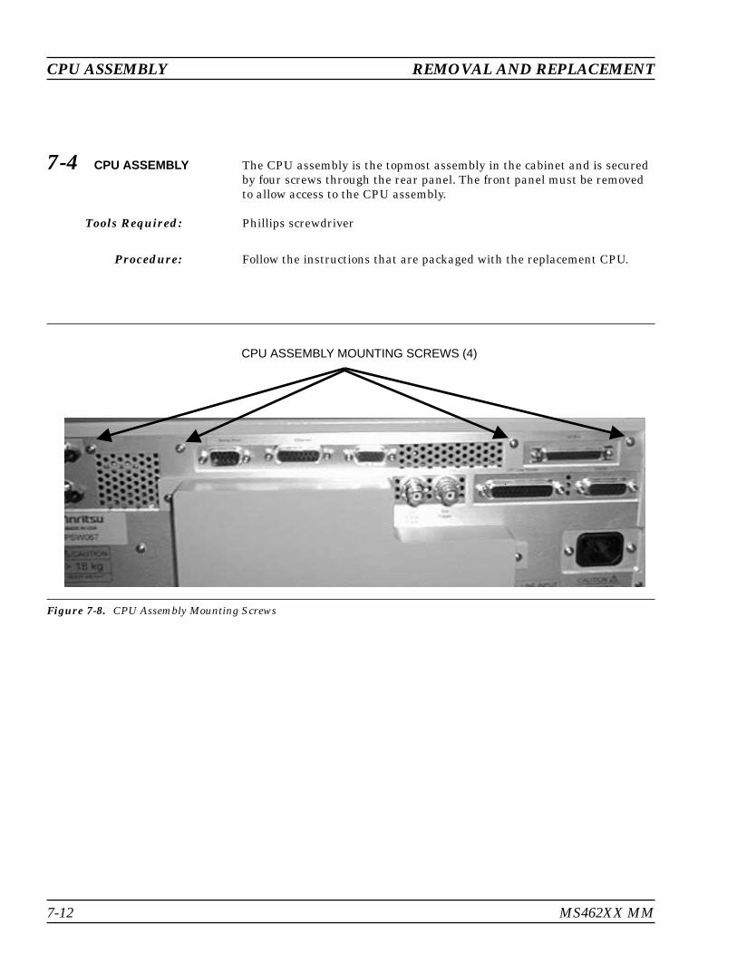
7-4 CPU ASSEMBLY The CPU assembly is the topmost assembly in the cabinet and is securedby four screws through the rear panel. The front panel must be removedto allow access to the CPU assembly.
Tools Required: Phillips screwdriver
Procedure: Follow the instructions that are packaged with the replacement CPU.
7-12 MS462XX MM
CPU ASSEMBLY REMOVAL AND REPLACEMENT
Figure 7-8. CPU Assembly Mounting Screws
CPU ASSEMBLY MOUNTING SCREWS (4)

With the CPU assembly removed from the system, the following subassem-blies can be removed and replaced:
REMOVAL AND REPLACEMENT CPU ASSEMBLY
MS462XX MM 7-13
Figure 7-9. CPU Assembly Removal and Cables
LCD BACKLIGHT CABLE INTERFACE PCB CABLE
LCD FLEX CABLE FLOPPY DISK DRIVE CABLE

System FirmwarePROM
The system operating firmware is stored in the System Firmware PROM(U75). The PROM may be changed to update or repair the system firm-ware as necessary.
Tools Required: PLCC IC Removal/Insertion Tool
Procedure: Locate and remove the System Firmware PROM (location 14 below) usingthe PLCC IC Removal Tool.
Replacement is the opposite of removal.
7-14 MS462XX MM
CPU ASSEMBLY REMOVAL AND REPLACEMENT
24
25
22
13
11
109
87
6
5 3
1
2
TO FRONT
PANEL BOARD
(D43018)
MAIN CPU:
1 - MC68040 CPU
2 - DRAM CONTROLLER
3 - 16 MB LOCAL DRAM
4 - 48 MB EXP. DRAM
5 - 4 MB NON-VOL SRAM
6 - 3V LITHIUM BATTERY
7 - CS PLD
8 - SCSI CONTROLER (OPT.)
9 - INTERRUPT CONTROLLER
10 - LAN CONTROLLER
11 - PERIPHERAL BUS SIZER
12 - 10 MB FLASH
13 - OPTION/MODEL SWITCHES
14 - BOOT EPROM
15 - MASTER/SLAVE GPIB CTRLS
16 - KEYBOARD CTRL
17 - FLOPPY DISK CTRL
18 - STATE MACHINE
19 - SERIAL PORT CTRL
DSP CORE:
20 - TMS320C44 DSP
21 - 2 MB LOCAL SRAM
22 - 512 KB LOCAL EPROM
23 - 128 KB GLOBAL SRAM
24 - DSP PLD
25 - DSP COMM ADC PLD
GRAPHICS CORE:
30 - TMS34020 GRAPHICS PROC.
31 - 1 MB DRAM
32 - 1 MB LOCAL VRAM
33 - PALETTE
34 - GSP PLD
35 - LCD PLD
4
20
30
12
21
23
31
32
33
34
35
14
15
16
17
18
19
TO LCD
BKLGHT
TO LCD
FLEX CABLE
(D43020)
TO SYSTEM
MOTHERBOARD
TO CONNECTOR
BOARD (D43017)
Figure 7-10. CPU Assembly Part Locator

CPU Heatsink withFan
The system CPU is protected by a thermal heat sink and fan combination.The heatsink with fan may be replaced as necessary.
Tools Required: None
Procedure: Locate and remove the CPU heatsink and fan assembly (location 1, Fig-ure 7-10).
Replacement is the opposite of removal.
Lithium Battery The system battery should be replaced every three years, or as necessary.
Tools Required: None
Procedure: Prior to replacing the CPU battery, it is important to copy all the harddrive files to floppy disks for temporary storage. Generally, one1.44 MByte floppy disk will be sufficient.
Use the following procedure to copy all the files from the internal harddrive. An external keyboard connected to the MS462XX will make theprocedure easier:
1. To view the contents of the internal SRAM disk, press the Utility key,then select:
GENERAL DISK UTILITIES
DISPLAY DIRECTORY
Note if there is any sub-directory.
2. Press the COMMAND LINE soft key.
3. Insert a blank formatted floppy disk into the MS462XX floppy drive.
4. Use the external keyboard to type:
COPY C:\*.* A:
5. Press the Enter key on the external keyboard to execute the copycommand.
6. If there is sub-directory on the SRAM disk, type:
CD C:\directory name
7. Repeat Steps 4 and 5 to copy the files in the sub-directory.
REMOVAL AND REPLACEMENT CPU ASSEMBLY
MS462XX MM 7-15

8. If the instrument is fitted with Option 4X, press the Appl key and se-lect:
CHANGE APPLICATION SETUP
MEASUREMENT TYPE TRANSMISSION AND REFLECTION
NOISE FIGURE / NOISE FIGURE SETUP
ENR TABLE OPERATIONS
SAVE ENR TABLE
TO FLOPPY DISK
9. Save the following three files to floppy disk:
� Vendor ENR Table� Internal ENR Extension Table� External ENR Extension Table
NOTESSome of the ENR files may have been stored on the harddisk; however, ENR files are not normally stored on the harddisk. The External ENR Extension Table file will only exist if ithas been created by the user. To completely backup all thefiles on the hard disk, it is essential that all of the previoussteps be completed.
10. Remove the CPU board from the instrument as described in Sec-tion 7-4.
11. Remove the drops of RTV compound which hold the lithium batteryin place. Gently slide the battery sideways (gently lift up on the re-taining clip only a small since excess lifting will reduce contact pres-sure on the new battery).
12. Install a new battery and hold it in place with three drops of RTVcompound, as before.
13. Reassemble the instrument.
14. Turn the instrument ON and press UTILITY MENU and select FOR-MAT HARD DRIVE.
15. After formatting the hard drive, reload all files from the floppy diskback onto the hard drive.
7-16 MS462XX MM
CPU ASSEMBLY REMOVAL AND REPLACEMENT

16. If the instrument is fitted with Option 4X, press the Appl key, select:
CHANGE APPLICATION SETUP
MEASUREMENT TYPE TRANSMISSION AND REFLECTION
NOISE FIGURE
NOISE FIGURE SETUP
ENR TABLE OPERATIONS
LOAD ENR TABLE
FROM FLOPPY DISK
17. Load the files that were saved to the floppy disk in Step 9 (VendorENR Table, Internal ENR Extension Table, and optional ExternalENR Extension Table).
NOTEIt is not sufficient to simply save these files to the hard drive.They must be loaded using the method described in thissection.
The battery replacement operation is complete
REMOVAL AND REPLACEMENT CPU ASSEMBLY
MS462XX MM 7-17

7-5 RECEIVER MODULEASSEMBLY
The receiver assembly is the bottom assembly in the cabinet and is se-cured by two screws through the rear panel. The front panel must be re-moved to allow access to the receiver assembly.
Tools Required: Phillips screwdriver
Procedure: 1. Remove the AC power cord.
2. Remove the front panel assembly (refer to Section 7-2).
3. Disconnect any cables connecting the option or source module to thereceiver module in the instrument. Make note of the position andorientation for all of the cables removed.
4. Remove the two rear panel mounting screws that secure the receivermodule (Figure 7-11).
7-18 MS462XX MM
RECEIVER MODULE ASSEMBLY REMOVAL AND REPLACEMENT
Figure 7-11. Receiver Module Mounting Screws (2)
RECEIVERM O D U L EMOUNTINGSCREW
RECEIVERM O D U L EMOUNTINGSCREW

5. Carefully pull the receiver module straight out from the front of theinstrument (Figure 7-12).
Replacement is the opposite of removal.
NOTEIndividual modules mounted on the Receiver Assembly mayvary according to the configuration of a particular system.
REMOVAL AND REPLACEMENT RECEIVER MODULE ASSEMBLY
MS462XX MM 7-19
Figure 7-12. Receiver Module Removal
RECEIVERMODULE

7-6 TEST PORTCONNECTOR ANDPORT MODULE
The following procedure describes the proper steps to remove and installthe Test Port Connector and Port Module.
Tools Required: � Anritsu 01-202 universal adapter wrench� 5/8” open end wrench� 5/8” open end torque wrench, 120 in-lb� 5/16” open end torque wrench, 8 in-lb
RemovalProcedure:
1. Remove the Port Module mounting screws from the receiver PCB.
2. Loosen the RF cables connected to the Port Module.
3. Loosen the K connection between the Port Module and the Test PortConnector and carefully slide the Port Module backward. Removethe Port Module.
4. Use the 5/8” open end wrench to loosen the Test Port connectormounting nut. This nut is on the back side of the Test Port connec-tor.
5. Remove the Test Port Connector.
InstallationProcedure:
1. Install the Test Port Connector through the D-shape hole on the Re-ceiver metal tray.
2. Install the Test Port connector mounting nut and tighten the nutslightly.
3. Place the Port Module with the “P” port facing the Test Port connec-tor. Connect the Port Module “P” port to the Test Port connector.Make the connection finger tight and then loosen a quarter turn.While making the connection, keep the Port Module flat against thereceiver PCB and be careful not to damage the center pin of the PortModule “P” port connector.
4. Install the Port Module mounting screws only far enough to hold themodule flat but still allowing some movement front to back.
5. Use the 5/8” wrench on the Test Port connector mounting nut, whileusing the universal adapter wrench in front to hold the Test Portconnector still. Tighten the mounting nut as tight as you can whileholding the Port Module flat against the receiver PCB with yourother fingers.
6. Use the 5/8” torque wrench to tighten the mounting nut to 120 in-lb.
7-20 MS462XX MM
TEST PORT CONNECTOR AND PORT MODULE REMOVAL AND REPLACEMENT

7. Use the 5/16” torque wrench to tighten the connection between theTest Port connector and the Port Module to 8 in-lb.
8. Tighten the Port Module mounting screws.
7-7 OPTION ANDSOURCE MODULES
The MS462XX Vector Network Measurement System option and sourcemodules are secured by Phillips screws through the rear panel. The frontpanel and the Receiver Module Assembly must be removed to allow re-moval of the option and source modules. There are three modules referredto in this procedure: The A2 Option Module, the Option Source Module,and the Source Module.
Tools Required: Phillips screwdriver
Procedure: 1. Remove the AC power cord.
2. Remove the front panel assembly (refer to Section 7-2).
3. Disconnect any cables connecting the option or source module to theother modules in the instrument. Make note of the position and ori-entation of all cables removed.
4. Remove the Receiver Module Assembly (refer to Section 7-5).
5. Remove the rear panel mounting screws for the Option or SourceModule to be removed (Figure 7-13 on the following page).
6. For the main Source Module, remove the backplane cover and thetwo Phillips flat head screws near the backplane PCB.
7. Carefully pull the option or source module straight out from thefront of the instrument (Figure 7-14 on the following page).
Replacement is the opposite of removal.
REMOVAL AND REPLACEMENT OPTION AND SOURCE MODULES
MS462XX MM 7-21
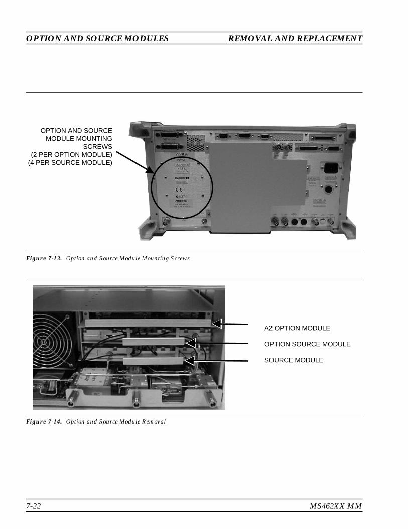
7-22 MS462XX MM
OPTION AND SOURCE MODULES REMOVAL AND REPLACEMENT
Figure 7-13. Option and Source Module Mounting Screws
OPTION AND SOURCEMODULE MOUNTING
SCREWS(2 PER OPTION MODULE)
(4 PER SOURCE MODULE)
Figure 7-14. Option and Source Module Removal
A2 OPTION MODULE
OPTION SOURCE MODULE
SOURCE MODULE
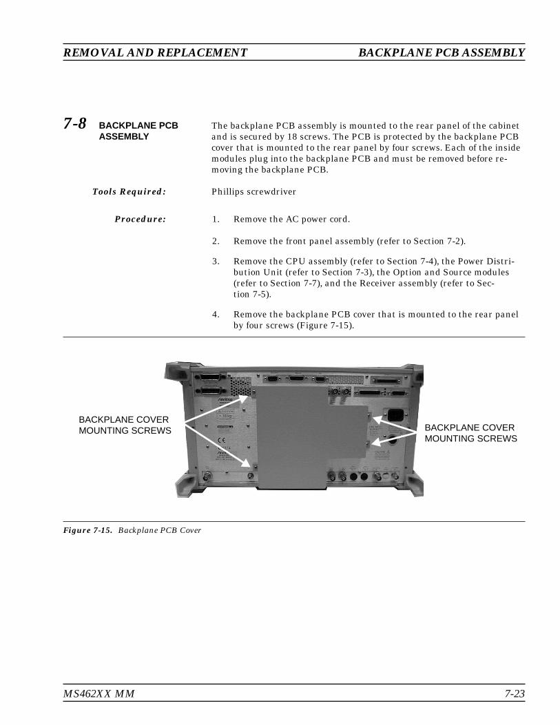
7-8 BACKPLANE PCBASSEMBLY
The backplane PCB assembly is mounted to the rear panel of the cabinetand is secured by 18 screws. The PCB is protected by the backplane PCBcover that is mounted to the rear panel by four screws. Each of the insidemodules plug into the backplane PCB and must be removed before re-moving the backplane PCB.
Tools Required: Phillips screwdriver
Procedure: 1. Remove the AC power cord.
2. Remove the front panel assembly (refer to Section 7-2).
3. Remove the CPU assembly (refer to Section 7-4), the Power Distri-bution Unit (refer to Section 7-3), the Option and Source modules(refer to Section 7-7), and the Receiver assembly (refer to Sec-tion 7-5).
4. Remove the backplane PCB cover that is mounted to the rear panelby four screws (Figure 7-15).
REMOVAL AND REPLACEMENT BACKPLANE PCB ASSEMBLY
MS462XX MM 7-23
Figure 7-15. Backplane PCB Cover
BACKPLANE COVERMOUNTING SCREWS BACKPLANE COVER
MOUNTING SCREWS
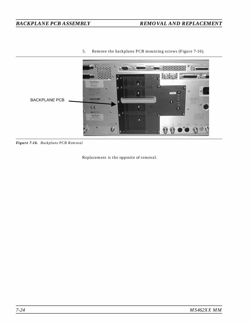
5. Remove the backplane PCB mounting screws (Figure 7-16).
Replacement is the opposite of removal.
7-24 MS462XX MM
BACKPLANE PCB ASSEMBLY REMOVAL AND REPLACEMENT
Figure 7-16. Backplane PCB Removal
BACKPLANE PCB

Table of Contents
A-1 INTRODUCTION . . . . . . . . . . . . . . . . . . . . . . . . . . . . . . . . . . . A-3
A-2 CONNECTOR CARE AND HANDLING . . . . . . . . . . . . . . . . . . . . . . . A-3Beware of Destructive Pin Depth of Mating Connectors. . . . . . . . . . . . . A-3Avoid Over-Torquing Connectors . . . . . . . . . . . . . . . . . . . . . . . . . A-4Cleaning Connectors . . . . . . . . . . . . . . . . . . . . . . . . . . . . . . . A-5
Appendix AConnector Care and Handling


Appendix AConnector Care and Handling
A-1 INTRODUCTION This appendix provides information on the proper care and handling ofRF sensor connectors.
A-2 CONNECTORCARE ANDHANDLING
Anritsu Vector Network Measurement Systems are high-quality, precisionlaboratory devices and should receive the care and respect normally af-forded such devices. Follow the precautions listed below when handling orconnecting these devices. Complying with these precautions will guaran-tee longer component life and less equipment downtime due to connectoror device failure. Also, such compliance will ensure that Vector NetworkMeasurement System failures are not due to misuse or abuse—two fail-ure modes not covered under the Anritsu warranty.
Beware ofDestructive Pin
Depth of MatingConnectors.
Based on RF components returned for repair, destructive pin depth ofmating connectors is the major cause of failure in the field. When a RFcomponent connector is mated with a connector having a destructive pindepth, damage will usually occur to the RF component connector. A de-structive pin depth is one that is too long in respect to the reference planeof the connector (Figure A-1).
The center pin of a precision RF component connector has a precision tol-erance measured in mils (1/1000 inch). The mating connectors of variousRF components may not be precision types. Consequently, the center pinsof these devices may not have the proper depth. The pin depth of DUTconnectors should be measured to assure compatibility before attemptingto mate them with a Vector Network Measurement System or sensor con-nectors. An Anritsu Pin Depth Gauge (Figure A-2), or equivalent, can beused for this purpose.
MS462XX MM A-3
01
2
3
45
1
2
3
4
21 1
2
Figure A-1. Pin Depth Gauge

If the measured connector is out of tolerance in the “+” region of the outerscale, the center pin is too long (see Table A-1). Mating under this condi-tion will likely damage the precision RF component connector. If the testdevice connector measures out of tolerance in the “–” region, the centerpin is too short. This should not cause damage, but it will result in a poorconnection and a consequent degradation in performance.
AvoidOver-Torquing
Connectors
Over-torquing connectors may damage the connector center pin. Fin-ger-tight is usually sufficient for Type N connectors. Always use a connec-tor torque wrench (8 inch-pounds) when tightening 3.5 mm type connec-tors. Never use pliers to tighten connectors.
A-4 MS462XX MM
CONNECTOR CARE AND HANDLING
REFERENCEPLANE
MALE
PINDEPTH
(INCHES)
REFERENCEPLANE
FEMALE
PINDEPTH
(INCHES)
Figure A-2. N Connector Pin DepthDefinition
Test PortConnector Type
Pin Depth(Inches)
Pin DepthGauge Reading*
(Inches)
N-Male 0.208 to 0.215–0.001–0.008
N-Female 0.204 to 0.207+0.000–0.003
3.5 mmMale and Female
0.000 to –0.005+0.000–0.005
GPC-7 0.000 to –0.003+0.000–0.003
* N connector readings are based on the Anritsu N-type guage block of 0.207-inches.
Table A-1. Allowable Test Port Connector Pin Depth

CleaningConnectors
The precise geometry that makes the RF component's high performancepossible can be easily disturbed by dirt and other contamination adheringto the connector interfaces. To clean the connector interfaces, use a cleancotton swab that has been dampened with denatured alcohol.
NOTEMost cotton swabs are too large to fit in the smaller connec-tor types. In these cases, it is necessary to peel off most ofthe cotton and then twist the remaining cotton tight. Be surethat the remaining cotton does not get stuck in the connec-tor. Cotton swabs of the appropriate size can be purchasedthrough a medical laboratory-type supply center.
The following are some important tips on cleaning connectors:
� Use only denatured alcohol as a cleaning solvent.� Do not use excessive amounts of alcohol as prolonged drying of
the connector may be required.� Never put lateral pressure on the center pin of the connector.� If installed, do not disturb the Teflon washer on the center con-
ductor pin.� Verify that no cotton or other foreign material remains in the
connector after cleaning it.� If available, carefully use compressed air to remove foreign parti-
cles and to dry the connector.� After cleaning, verify that the center pin has not been bent or
damaged.
CONNECTOR CARE AND HANDLING
MS462XX MM A-5/A-6


Appendix BPerformance Specifications


Subject Index
#10 MHz
calibration . . . . . . . . . . . . . . . . 5-4 to 5-7clock distribution . . . . . . . . . . . . . . . 2-14
37SF50 phase harmonic standards check . . . . 3-36
AADC clock generation . . . . . . . . . . . . . . 2-14
ALCadjustment. . . . . . . . . . . . . . . . 5-8 to 5-9calibration . . . . . . . . . . . . . . . . . . . 5-3circuit description . . . . . . . . . . . . . . . 2-8
analog monitor . . . . . . . . . . . . . . . . . . 2-12
assembly exchange program . . . . . . . . . . . 1-7
attenuator write-in values . . . . . . . . . . . . 3-23
automatic calibration . . . . . . . . . . . . . . . 5-5
auto-reversing module . . . . . . . . . . . . . . 2-15
Bback-end attenuator calibration . . . . . . . 5-3,5-10
backlightdriver PCB removal . . . . . . . . . . . . . . 7-7fluorescent lamp removal . . . . . . . . . . . 7-8
backplane removal . . . . . . . . . . . . . . . . 7-23
batterylife . . . . . . . . . . . . . . . . . . . . . . . . 1-7replacement . . . . . . . . . . . . . . . . . . 7-15
block diagrams9 GHz down conversion module . . . . . . . 2-479 GHz switched tripler . . . . . . . . . . . . 2-47CPU module . . . . . . . . . . . . . . . . . . 2-26MS4622A . . . . . . . . . . . . . . . 2-27 to 2-28MS4622B . . . . . . . . . . . . . . . 2-29 to 2-33MS4622C . . . . . . . . . . . . . . . 2-41 to 2-42MS4622D . . . . . . . . . . . . . . . . . . . 2-45MS4623A/MS4624A . . . . . . . . . 2-34 to 2-35MS4623B/MS4624B . . . . . . . . . 2-36 to 2-40
MS4623C/MS4624C . . . . . . . . . 2-43 to 2-44MS4623D/MS4624D . . . . . . . . . . . . . 2-46
bounding circuitry . . . . . . . . . . . . . . . . . 2-6
Ccalibration
10 MHz. . . . . . . . . . . . . . . . . . 5-3 to 5-7ALC adjustment . . . . . . . . . . . 5-3,5-8 to 5-9automatic . . . . . . . . . . . . . . . . . . . . 5-5back-end attenuator . . . . . . . . . . . 5-3,5-10conditions . . . . . . . . . . . . . . . . . . 4-4,5-4manual . . . . . . . . . . . . . . . . . . . . . 5-6noise source signal through path . . . . . . . 5-3noise source through path characterization . 5-11precautions . . . . . . . . . . . . . . . . . . . 4-4pre-test setup . . . . . . . . . . . . . . . . . . 5-4
central processor module. . . . . . . . . . . . . 2-25
common offset mode . . . . . . . . . . . . . . . . 2-8
components layout, receiver module . . . . . . . 6-19
compression level test . . . . . . . . . . 3-16 to 3-18
conditions for calibration . . . . . . . . . . . 4-4,5-4
configurationsMS462XA . . . . . . . . . . . . . . . . . . . 2-17MS462XB . . . . . . . . . . . . . . . . . . . 2-17MS462XC . . . . . . . . . . . . . . . . . . . 2-18MS462XD . . . . . . . . . . . . . . . . . . . 2-19switched module . . . . . . . . . . . . . . . 2-16
connectorcare and handling . . . . . . . . . . . . . . . A-3cleaning. . . . . . . . . . . . . . . . . . . . . A-5
conventions . . . . . . . . . . . . . . . . . . . . 1-10
CPUheatsink and fan removal. . . . . . . . . . . 7-15removal . . . . . . . . . . . . . . . . . . . . 7-12troubleshooting . . . . . . . . . . . . . . . . . 6-4
MS462XX MM Index-1
SUBJECT INDEX # TO C

DDDS reference clock . . . . . . . . . . . . . . . . 2-6
descriptionsALC circuitry . . . . . . . . . . . . . . . . . . 2-8auto-reversing module . . . . . . . . . . . . 2-15bounding circuitry . . . . . . . . . . . . . . . 2-6central processor module . . . . . . . . . . . 2-25common offset mode . . . . . . . . . . . . . . 2-8DDS reference clock . . . . . . . . . . . . . . 2-6digital interface . . . . . . . . . . . . . . 2-5,2-10down conversion module . . . . . . . . . . . 2-10frequency bands . . . . . . . . . . . . . . . . 2-7frequency translating group delay
receiver . . . . . . . . . . . . . . . . . . 2-23synthesizer . . . . . . . . . . . . . . . . 2-22
front end RF components. . . . . . . 2-15 to 2-20harmonic generator mode . . . . . . . . . . . 2-9heterodyne oscillator . . . . . . . . . . . . . . 2-7high isolation switch module . . . . . . . . . 2-16low noise pre-amplifier . . . . . . . . . . . . 2-16main oscillator loops . . . . . . . . . . . . . . 2-5non-reversing module . . . . . . . . . . . . . 2-16offset oscillator loops . . . . . . . . . . . . . . 2-5option 3 - second source. . . . . . . . . . . . 2-20option 4 - noise figure measurement capability. . . . . . . . . . . . . . . . . . . . . . . . . 2-20option 6 - third test port . . . . . . . . . . . 2-21option modules . . . . . . . . . . . . 2-21 to 2-24port 3 module . . . . . . . . . . . . . . . . . 2-16port module . . . . . . . . . . . . . . . . . . 2-16receiver module . . . . . . . . . . . . 2-10 to 2-14receiver modules . . . . . . . . 2-25 to 2-26,2-47reference channel intermediate frequency path. . . . . . . . . . . . . . . . . . . . . . . . . 2-12source module . . . . . . . . . . . . . . 2-4 to 2-9speed-up circuitry . . . . . . . . . . . . . . . 2-7step attenuator . . . . . . . . . . . . . . . . 2-16switched
doubler module. . . . . . . . . . . . . . 2-15filters . . . . . . . . . . . . . . . . . . . 2-7module . . . . . . . . . . . . . . . . . . 2-16tripler module . . . . . . . . . . . . . . 2-15
test channel intermediate frequency path . . 2-11wideband noise figure receiver . . . . . . . . 2-23
digital interface. . . . . . . . . . . . . . . . 2-5,2-10
disk drive removal . . . . . . . . . . . . . . . . . 7-6
doubler . . . . . . . . . . . . . . . . . . . . . . 2-15
down conversion module description . . . . . . 2-10
DRAM troubleshooting . . . . . . . . . . . . . . 6-7
DSP communication port interface . . . . . . . 2-14
DSP SRAM, troubleshooting . . . . . . . . . . . 6-7
dynamic range, operational check . . . . 3-10 to 3-15
Eelectrostatic discharge (ESD) . . . . . . . . . . 1-12
exchange program . . . . . . . . . . . . . . . . . 1-7
extended flash memory, troubleshooting . . . . . 6-6
Ffan
assembly removal . . . . . . . . . . . . . . . 7-10CPU fan removal . . . . . . . . . . . . . . . 7-15
firmware removal. . . . . . . . . . . . . . . . . 7-14
flash memory, troubleshooting . . . . . . . . . . 6-6
floppy disk drive removal . . . . . . . . . . . . . 7-6
frequency bands . . . . . . . . . . . . . . . . . . 2-7
frequency translating group delaymeasurement . . . . . . . . . . . . . . . . . 3-35receiver . . . . . . . . . . . . . . . . . . . . 2-23synthesizer . . . . . . . . . . . . . . . . . . 2-22troubleshooting . . . . . . . . . . . . . . . . 6-27
front end RF components . . . . . . . . 2-15 to 2-20
front paneldescription . . . . . . . . . . . . . . . . . . . 2-4removal . . . . . . . . . . . . . . . . . 7-4 to 7-8troubleshooting . . . . . . . . . . . . . . . . 6-22
full reversing . . . . . . . . . . . . . . . . . . . . 1-3
fuse . . . . . . . . . . . . . . . . . . . . . . . . 7-11
GGPIB
function . . . . . . . . . . . . . . . . . . . . . 2-4
graphicsDRAM troubleshooting. . . . . . . . . . . . . 6-7
Index-2 MS462XX MM
D TO G SUBJECT INDEX
VRAM troubleshooting . . . . . . . . . . . . . 6-7
Hhardware troubleshooting. . . . . . . . . 6-8 to 6-22
harmonic generator mode . . . . . . . . . . . . . 2-9
harmonic output check . . . . . . . . . . . . . . 3-39
heat sink removal . . . . . . . . . . . . . . . . 7-15
heterodyne oscillator. . . . . . . . . . . . . . . . 2-7
high isolation switch module. . . . . . . . . . . 2-16
IIF signals. . . . . . . . . . . . . . . . . . . . . . 2-3
input/output return loss check . . . . . . . . . . 3-36
interface PCB removal. . . . . . . . . . . . . . . 7-7
intermediate frequency sampling . . . . . . . . 2-13
Kkeypad removal . . . . . . . . . . . . . . . . . . 7-7
LLCD
assembly removal . . . . . . . . . . . . . . . 7-6backlight driver PCB removal . . . . . . . . . 7-7troubleshooting . . . . . . . . . . . . . . . . 6-22
lithium battery replacement . . . . . . . . . . . 7-15
low noise pre-amplifier . . . . . . . . . . . . . . 2-16
Mmain oscillator loops . . . . . . . . . . . . . . . . 2-5
maintenance, preventive . . . . . . . . . . . . . 1-7
manual calibration. . . . . . . . . . . . . . . . . 5-6
manuals . . . . . . . . . . . . . . . . . . . . . . 1-3
measurement quality problems . . . . . . . . . 6-23
measurements . . . . . . . . . . . . . . . . . . . 2-3
models . . . . . . . . . . . . . . . . . . . . . . . 1-3
MS462XA receiver configuration . . . . . . . . 2-17
MS462XB receiver configuration . . . . . . . . 2-17
MS462XC receiver configuration . . . . . . . . 2-18
MS462XD receiver configuration . . . . . . . . 2-19
Nnegative noise figure, troubleshooting. . . . . . 6-24
noise figureassurance check . . . . . . . . . . . . . . . . 3-26measurement confidence check . . . 3-30 to 3-34measurement problems. . . . . . . . 6-24 to 6-26troubleshooting overload . . . . . . . . . . . 6-25
noise sourcepower supply troubleshooting . . . . . . . . 6-21signal through path calibration . . . . . . . . 5-3signal through path characterization . . . . 5-11
non-ratio parameter test . . . . . . . . . . 3-7 to 3-9
non-reversing module . . . . . . . . . . . . . . 2-16
not allowed message, troubleshooting . . . . . . 6-24
nyquist sampling theory . . . . . . . . . . . . . 2-13
Ooffset oscillator loops. . . . . . . . . . . . . . . . 2-5
operation modes . . . . . . . . . . . . . . . . . . 2-8
operational checkdynamic range . . . . . . . . . . . . 3-10 to 3-15
option 3—second source . . . . . . . . . . . . . 2-20
option 4—noise figure measurement . . . . . . 2-20
option 6—third test port . . . . . . . . . . . . . 2-21
option module removal . . . . . . . . . . . . . . 7-21
option modules, description . . . . . . . 2-21 to 2-24
optionsin models . . . . . . . . . . . . . . . . . . . . 1-3list of . . . . . . . . . . . . . . . . . . . . . . 1-4
PPDU
fuse . . . . . . . . . . . . . . . . . . . . . . 7-11removal . . . . . . . . . . . . . . . . . . . . . 7-9
MS462XX MM Index-3
SUBJECT INDEX H TO P
pin depthdefinition . . . . . . . . . . . . . . . . . . . . A-4destructive mating . . . . . . . . . . . . . . . A-3gauge . . . . . . . . . . . . . . . . . . . . . . A-3test port specifications . . . . . . . . . . . . . A-4
port 1/2 module . . . . . . . . . . . . . . . . . . 2-16
port 3 module . . . . . . . . . . . . . . . . . . . 2-16
port module removal . . . . . . . . . . . . . . . 7-20
power accuracy, verifying . . . . . . . . . . 3-5 to 3-6
power distribution unit, troubleshooting . . . . 6-21
precautions for calibration . . . . . . . . . . . . 4-4
pre-test setup for calibration . . . . . . . . . . . 5-4
preventive maintenance . . . . . . . . . . . . . . 1-7
PROM removal . . . . . . . . . . . . . . . . . . 7-14
Rraw receiver noise figure check . . . . . . . . . 3-26
receiver magnitude display test . . . . . 3-19 to 3-25
receiver moduleblock diagrams . . . . . . . . . 2-25 to 2-26,2-47components layout . . . . . . . . . . . . . . 6-19configurations . . . . . . . . . . . . . . . . . 2-16description . . . . . . . . . . . . . . 2-10 to 2-14removal . . . . . . . . . . . . . . . . . . . . 7-18troubleshooting . . . . . . . . . . . . . . . . 6-16
recommended test equipment . . . . . . . 1-7 to 1-9
reference channel IF path . . . . . . . . . . . . 2-12
related manuals . . . . . . . . . . . . . . . . . . 1-3
removal and replacement . . . . . . . . . . . . . 7-3
repair . . . . . . . . . . . . . . . . . . . . . . . . 7-3
RFcomponent control. . . . . . . . . . . . . . . 2-14connector handling. . . . . . . . . . . . . . . A-3front end components. . . . . . . . . 2-15 to 2-20
Ssampling of the intermediate frequency. . . . . 2-13
sampling theory, nyquist . . . . . . . . . . . . . 2-13
self test . . . . . . . . . . . . . . . . . . . . . . . 6-3
serial number . . . . . . . . . . . . . . . . . . . 1-10
servicelist of service centers . . . . . . . . . . . . . 1-13policy . . . . . . . . . . . . . . . . . . . . . . 1-4
service logchecking. . . . . . . . . . . . . . . . . . . . . 3-3description . . . . . . . . . . . . . . . . . . . 2-4
softwareproblems. . . . . . . . . . . . . . . . . . . . 6-23version . . . . . . . . . . . . . . . . . . . . . 1-10
source 1 power write-in values . . . . . 3-23 to 3-25
source moduledescription . . . . . . . . . . . . . . . . 2-4 to 2-9removal . . . . . . . . . . . . . . . . . . . . 7-21RF output specifications . . . . . . . . . . . . 2-4troubleshooting . . . . . . . . . . . . . . . . . 6-9
spare parts listing. . . . . . . . . . . . . . 1-5 to 1-6
speed-up circuitry . . . . . . . . . . . . . . . . . 2-7
SRAM, troubleshooting . . . . . . . . . . . . . . 6-6
standard calibration conditions . . . . . . . . . . 4-4
step attenuator . . . . . . . . . . . . . . . . . . 2-16
switch module, high isolation . . . . . . . . . . 2-16
switchedfilters . . . . . . . . . . . . . . . . . . . . . . 2-7frequency doubler module . . . . . . . . . . 2-15frequency tripler module . . . . . . . . . . . 2-15module . . . . . . . . . . . . . . . . . . . . . 2-16
systemcabling . . . . . . . . . . . . . . . . . . . . . 6-20dynamic range test . . . . . . . . . . 3-10 to 3-15firmware PROM removal . . . . . . . . . . . 7-14information . . . . . . . . . . . . . . . . . . 1-10overview . . . . . . . . . . . . . . . . . . . . 2-3
Ttest
compression level . . . . . . . . . . . 3-16 to 3-18receiver magnitude display. . . . . . 3-19 to 3-25system dynamic range . . . . . . . . 3-10 to 3-15
test channel intermediate frequency path . . . 2-11
Index-4 MS462XX MM
R TO T SUBJECT INDEX

test equipmentfor calibration. . . . . . . . . . . . . . . . . . 5-4recommended for service . . . . . . . . 1-7 to 1-9
test port connectorconfigurations . . . . . . . . . . . . . . . . . 2-15removal . . . . . . . . . . . . . . . . . . . . 7-20
transmission/reflection . . . . . . . . . . . . . . 1-3
tripler . . . . . . . . . . . . . . . . . . . . . . . 2-15
troubleshooting10 MHz reference oscillator . . . . . . . . . 6-18ALC . . . . . . . . . . . . . . . . . . . . . . 6-13CPU module . . . . . . . . . . . . . . . . 6-4,6-8DRAM. . . . . . . . . . . . . . . . . . . . . . 6-7DSP SRAM . . . . . . . . . . . . . . . . . . . 6-7extended flash memory . . . . . . . . . . . . 6-6flash memory . . . . . . . . . . . . . . . . . . 6-6floppy drive read/write . . . . . . . . . . . . 6-22frequency translating group delay . . . . . . 6-27front panel. . . . . . . . . . . . . . . . . . . 6-22GPIB . . . . . . . . . . . . . . . . . . . . . . 6-9GPIB Address Retention . . . . . . . . . . . . 6-9graphics DRAM. . . . . . . . . . . . . . . . . 6-7graphics VRAM. . . . . . . . . . . . . . . . . 6-7hardware . . . . . . . . . . . . . . . . 6-8 to 6-22internal/external noise source measurement 6-25LCD . . . . . . . . . . . . . . . . . . . . . . 6-22measurement quality problems . . . . . . . 6-23menu . . . . . . . . . . . . . . . . . . . . . . 6-4
negative noise figure . . . . . . . . . . . . . 6-24noise figure
assurance. . . . . . . . . . . . . . . . . 6-25confidence . . . . . . . . . . . . . . . . 6-26measurement problems . . . . . 6-24 to 6-26overload . . . . . . . . . . . . . . . . . 6-25response . . . . . . . . . . . . . . . . . 6-25ripple . . . . . . . . . . . . . . . . . . . 6-25
noise source power supply . . . . . . . . . . 6-21non-ratio parameter test . . . . . . . . 3-7 to 3-9not allowed message . . . . . . . . . . . . . 6-24phase-lock loop . . . . . . . . . . . . . . . . 6-10power distribution unit . . . . . . . . . . . . 6-21printer . . . . . . . . . . . . . . . . . . . . . 6-9raw receiver noise figure . . . . . . . . . . . 6-26receiver module . . . . . . . . . . . . . . . . 6-16RF components . . . . . . . . . . . . . . . . 6-19software problems. . . . . . . . . . . . . . . 6-23source module . . . . . . . . . . . . . . . . . 6-9SRAM . . . . . . . . . . . . . . . . . . . . . . 6-6
Vverification
output power accuracy . . . . . . . . . 3-5 to 3-6
verify ALC calibration . . . . . . . . . . . . . . 6-14
Wwideband noise figure receiver. . . . . . . . . . 2-23
MS462XX MM Index-5/Index-6
SUBJECT INDEX V TO W