Embed Size (px)
Citation preview
UCRL-CONF-225806
MRF Applications: On the Road toMaking Large-Aperture Ultraviolet LaserResistant Continuous Phase Plates forHigh-Power Lasers
J. A. Menapace, P. J. Davis, W. A. Steele,M. R. Hachkowski, A. Nelson, K. Xin
October 26, 2006
Boulder Damage SymposiumBoulder, CO, United StatesSeptember 25, 2006 through September 27, 2006

Disclaimer
This document was prepared as an account of work sponsored by an agency of the United States Government. Neither the United States Government nor the University of California nor any of their employees, makes any warranty, express or implied, or assumes any legal liability or responsibility for the accuracy, completeness, or usefulness of any information, apparatus, product, or process disclosed, or represents that its use would not infringe privately owned rights. Reference herein to any specific commercial product, process, or service by trade name, trademark, manufacturer, or otherwise, does not necessarily constitute or imply its endorsement, recommendation, or favoring by the United States Government or the University of California. The views and opinions of authors expressed herein do not necessarily state or reflect those of the United States Government or the University of California, and shall not be used for advertising or product endorsement purposes.

MRF Applications: On the Road to Making Large-Aperture Ultraviolet Laser Resistant Continuous Phase Plates for
High-Power Lasers
Joseph A. Menapace*a, Pete J. Davisa, William A. Steelea, M. Roman Hachkowskib, Andrew Nelsonb, and Kai Xinb
aUniversity of California, Lawrence Livermore National Laboratory
*P.O. Box 808, 7000 East Avenue, L-491, Livermore, CA 94550 925-423-0829 ([email protected])
bZygo Corporation, P.O. Box 448, Middlefield, CT 06455-0448
Work performed under the auspices of the US Department of Energy by Lawrence Livermore National
Laboratory under contract No. W-7405-ENG-48.
ABSTRACT Over the past two years we have developed MRF tools and procedures to manufacture large-aperture (430 X 430 mm) continuous phase plates (CPPs) that are capable of operating in the infrared portion (1053 nm) of high-power laser systems. This is accomplished by polishing prescribed patterns of continuously varying topographical features onto finished plano optics using MRF imprinting techniques. We have been successful in making, testing, and using large-aperture CPPs whose topography possesses spatial periods as low as 4 mm and surface peak-to-valleys as high as 8.6 µm. Combining this application of MRF technology with advanced MRF finishing techniques that focus on ultraviolet laser damage resistance makes it potentially feasible to manufacture large-aperture CPPs that can operate in the ultraviolet (351 nm) without sustaining laser-induced damage. In this paper, we will discuss the CPP manufacturing process and the results of 351-nm/3-nsec equivalent laser performance experiments conducted on large-aperture CPPs manufactured using advanced MRF protocols. Keywords: subsurface damage, MRF, surface imperfections, laser-induced damage, continuous phase plates, diffractive optics, phase screens, far-field characteristics, speckle
1. INTRODUCTION High-powered laser systems utilized for inertial confinement fusion (ICF) research, such as the Nation Ignition Facility (NIF) at Lawrence Livermore National Laboratory, Laser MegaJoule (CEA) near Bordeaux, France, and OMEGA at the Laboratory for Laser Energetics (LLE) require precise characterization and control of the laser beam illumination at the target plane. Our group has been successful in the past two years at developing advanced Magnetorheological Finishing (MRF) technology to accurately apply complex topographical patterns onto optical surfaces that can be used to manipulate and control laser beam-shapes, energy distributions, and wavefront profiles. The most interesting and direct application of this advanced technology is its use in the manufacture of large-aperture (430 X 430 mm) custom continuous phase plates (CPPs) to improve on-target irradiation uniformity which, in turn, reduces hydrodynamic instabilities that develop during ICF implosions1-3. Prior work on phase plates for large-aperture high-power laser systems combined mask resist and etching technologies to imprint phase manipulating patterns onto optics. Lower efficiency forerunners of the CPP
employed a resist masking and acid etching approach to imprint binary4,5 (rectangular/hexagonal phase plate structure) and 16 level step patterns6,7 (kinoform phase plate) onto fused silica surfaces similar to that used in the fabrication of integrated circuit boards. This approach was replaced by masking and resistive ion etching techniques that were capable of imprinting higher efficiency CPP patterns onto optics for use at the Laboratory for Laser Energetics8,9 and the Laser MegaJoule facility10. MRF offers a direct approach for imprinting smooth topographical features onto optics without the use of masks or master plates. Its deterministic polishing capability and close interplay with interferometry enable imprinting of diffractive phase structure that varies continuously across the whole beam aperture with no sharp discontinuities or phase anomalies. The technology is capable of, and routinely produces, highly accurate topographical profiles with errors of about 30 nm rms over the optic aperture that yields highly efficiency plates (> 99 percent) whose characteristics are precisely defined. Our MRF imprinting development has mainly focused on manufacture of CPPs for use in the infrared portion (1053 nm) of high-power laser systems11. Combining this technology with advanced MRF finishing techniques that focus on ultraviolet laser damage resistance12 makes it potentially feasible to manufacture large-aperture CPPs that can operate in the ultraviolet (351 nm) without sustaining laser-induced damage. In the following sections, we will give a brief overview of what CPPs do in large-aperture high-power lasers followed by a discussion on how they are manufactured using MRF. We will then present experimental results highlighting the quality of the imprinting process and damage performance observed on large-aperture CPPs manufactured and tested using 351-nm, 3-nsec equivalent, laser light. Lastly, we will discuss some of the artifacts that we have observed on a small number of CPPs produced and how they can be eliminated.
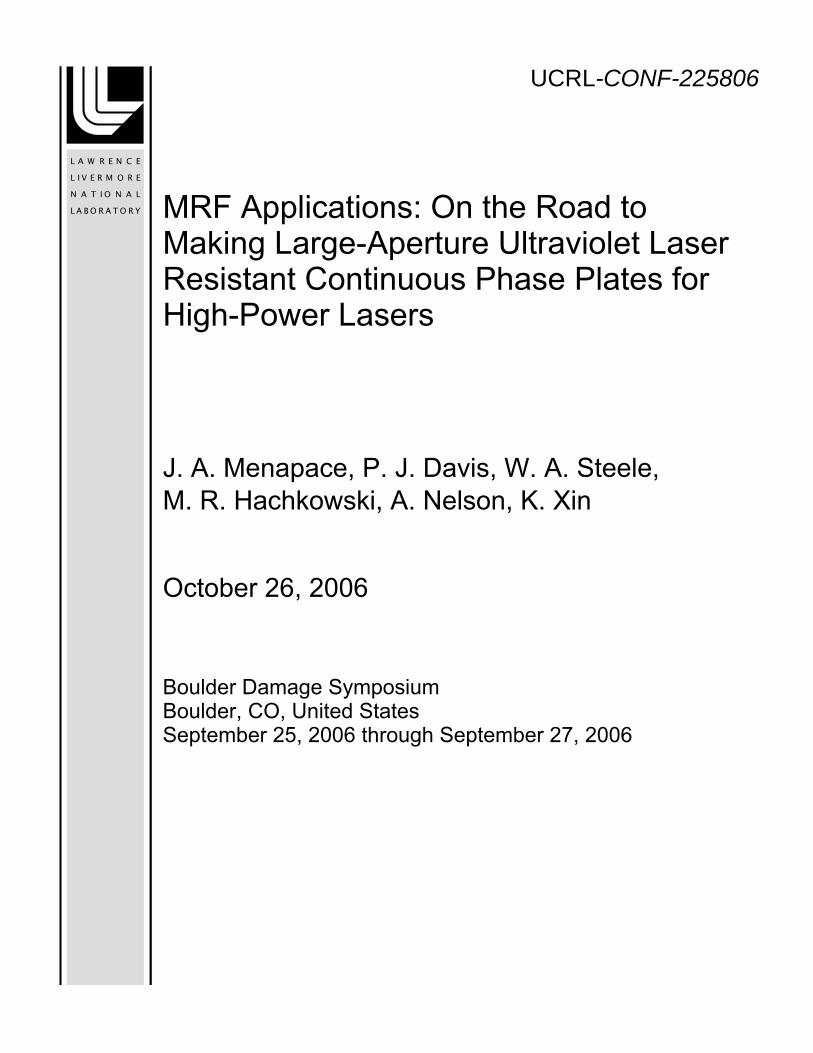
2. FUNCTIONALITY OF CPPs IN HIGH-POWER LASERS Custom CPPs are used in kilo-Joule and Mega-Joule class laser systems to achieve prescribed beam characteristics via manipulation of the incoming wavefront. They are typically used in the final optics portion of high-power laser systems to minimize non-linear gain and contrast modulation that can deteriorate laser beam performance as light propagates through the numerous optics comprising a beam line. CPPs function in combination with a focusing element to define the size and shape of the beam at focus, the wavefront characteristics (uniformity) at the focal plane, and the intensity of the beam within the focal spot. To eliminate wavefront discontinuities or high contrast inherent in previous discrete (stepped)4-7 plate designs, CPPs are made by imprinting a continuously varying phase profile onto an optical surface, Figure 1. This near-field topography is the key to enabling detailed control of the laser beam characteristics at the focal plane at high-power. It is designed to convert a square or circular laser beam footprint to an elliptical or circular spot of prescribed lateral dimensions. This continuously varying surface topography perturbs the incoming laser beam wavefront before passing through the final focusing element to yield a beam footprint at the focal plane with the desired characteristics.
Figure 1: Continuously varying topographical CPP pattern with an 8.6 µm P-V imprinted onto a 430 X 430 X 10 mm fused silica substrate using MRF. Top - transmitted wavefront phase map. Bottom - Surface height.

Different experimental conditions at the target plane in an ICF laser system require that several different plate designs be manufactured. These conditions include indirect and direct drive implosion cone beams and back-lighter/backscatter diagnostic beam drivers1-3. As such, CPPs are considered user prescribed optics and are tailored for each particular experiment. Figure 2 shows the far-field characteristics for three different CPP types that have been manufactured and tested at LLNL.
Figure 2: Large-aperture CPPs manufactured and tested at LLNL. Left - 50 degree outer cone implosion CPP, eccentricity of 0.56. Center - 23 degree inner cone implosion CPP, eccentricity of 0.88. Right - 2 mm far-field spot illuminator CPP, eccentricity of 1.00. The success of the MRF imprinting development is evident in these examples and shows that large-aperture CPPs can be routinely manufactured that meet the stringent specifications necessary for high-power laser ICF experiments. The far-field spots have high super-Gaussian order that defines a sharp beam boundary, typically greater than 6-7. ICF specifications require control of the far- field spot size to within +/- 15 µm at selected radii, typically at 80-, 90-, and 95-percent encircled energy. These CPPs spot sizes are well within the tolerance required with a maximum deviation of +/- 5 µm from nominal. Far-field spot size control is necessary in ICF applications to keep the laser beam from impinging upon critical components in the target area, to ensure that the total laser energy is in the desired range, and to establish the proper projection angles onto target for indirect drive. Beyond the size control, specifications and designs require laser beam wavefront/illumination control to better than 5 to 7 percent deviation (design dependent) within the far-field spot. Wavefront uniformity at the target plane needs to be established and controlled to maintain uniform laser energy across the spot illuminating the target, both short- and long-range, and to eliminate high intensity areas within the spot that can deteriorate hydrodynamic performance at the target.

Table 1: CPP performance parameters versus specification for large aperture CPPs manufactured using MRF
Specification Measured Pass/Fail 50 degree outer cone implosion CPP 80% Encircled Energy Radius (µm) 421.0 +/- 15.0 421.8 PASS 90% Encircled Energy Radius (µm) 472.0 +/- 15.0 476.2 PASS 95% Encircled Energy Radius (µm) 515.0 +/- 15.0 520.8 PASS
Individual Lineout RMS Deviation (%) 5.0 4.2 PASS 2D RMS Deviation over Central Area (%) 5.0 4.5 PASS 50 % Eccentricity (a = 451.2, b = 252.4) 0.56 +/- 0.1 0.56 PASS
23 degree inner cone implosion CPP 80% Encircled Energy Radius (µm) 594.0 +/- 15.0 592.3 PASS 90% Encircled Energy Radius (µm) 652.0 +/- 15.0 651.2 PASS 95% Encircled Energy Radius (µm) 696.0 +/- 15.0 696.2 PASS
Individual Lineout RMS Deviation (%) 7.0 5.9 PASS 2D RMS Deviation over Central Area (%) 5.0 4.7 PASS 50 % Eccentricity (a = 451.2, b = 252.4) 0.88 +/- 0.1 0.88 PASS
2 mm far-field spot illuminator CPP 80% Encircled Energy Radius (µm) 860.0 +/- 15.0 860.0 PASS 90% Encircled Energy Radius (µm) 923.0 +/- 15.0 925.4 PASS 95% Encircled Energy Radius (µm) 976.0 +/- 15.0 977.1 PASS
Individual Lineout RMS Deviation (%) 6.5 5.6 PASS 2D RMS Deviation over Central Area (%) 6.5 5.7 PASS 50 % Eccentricity (a = 451.2, b = 252.4) 1.02 +/- 0.1 1.02 PASS
3. LARGE-APERTURE CONTINUOUS PHASE PLATES MANUFACTURE Our development of CPP imprinting technology has, for the most part, focused upon applications where the CPPs are used in the infrared (1053 nm) portion of high-power laser systems and designed for far-field characteristics in the ultraviolet (351 nm)2,11. The CPP designs are, however, achromatic and can be used at any wavelength with nearly constant results. Small changes in the far-field characteristics arise, about 2 percent between the infrared and the ultraviolet, which are attributed to the ratio between substrate refractive index at the use wavelength and the design wavelength. They are typically within application tolerances and can be ignored. The main difficulty to overcome in using the CPPs in the ultraviolet is to prepare a substrate that has improved damage performance at the use wavelength. This requires a fabrication protocol incorporating advanced finishing techniques. In 2002, we introduced an advanced finishing process that exhibited superior damage performance of fused silica at 351 nm12. The process uses MRF final finishing on fused silica to attain final figure and superior damage performance once combined with HF acid etching to remove MRF related contaminants such as iron and ceria. Since MRF is used to imprint CPP topography, a logical extension on this would be to incorporate the same protocols used to make damage resistant fused silica substrates to CPP manufacture. To confirm our concept, we manufactured a “LLNL Proof of Principle” fused silica optic where we uniformly removed material from both sides of a damaged optic using MRF until all the damage was eliminated. This optic is a 140 X 140 X 10 mm fused silica substrate containing handling damage and previous laser-induced damage. After MRF removal of remove 95 µm of surface material, HF acid etching yielded an optic with no subsurface damage suggesting that CPPs could be fabricated for use in high-fluence ultraviolet applications, Figure 3.

The “LLNL Proof of Principle” optic was damage tested though 14 J/cm2 at 351-nm, 3-nsec equivalent fluence, in the LLNL Phoenix Damage Laboratory with no observed damage confirming that the MRF/etching process is feasible for the manufacture of ultraviolet laser resistant CPPs.
Figure 3: MRF polishing was used to remove 95 µm of surface material from the “LLNL Proof of Principle” optic to eliminate pre-existing damage from handling and previous laser damage testing. Left – polishing progress was tracked by monitoring the deepest fractures using optical microscopy. Right – damage maps before and after MRF polishing and etching illustrate the improvement is surface quality after removal of imperfections. CPPs used in the final portion of high-power lasers are typically large aperture optics; for example, in NIF, CPPs are 430 X 430 X 10 mm. Over the past two years the Zygo Corporation and LLNL have been developing a manufacturing process for large-aperture thin (10-15 mm thick) fused silica optics capable of operating at 351-nm laser fluences up to 14 J/cm2. This manufacturing process is designed around a detailed knowledge of subsurface damage arising from each process step in the manufacturing line13-16. During the development phase of this effort, subsurface damage was measured for each of the process steps, including cleaning, handling, grinding, and polishing, using MRF wedge techniques15 reported previously. Different process machine parameters, coolants, abrasive types, and pads were analyzed, selected, and optimized to take advantage of high material removal rates with minimum or manageable subsurface damage. Once the subsurface damage characteristics were obtained for each step, minimum material removal requirements were put into place on subsequent steps to completely remove subsurface damage from previous steps. Additional material removal beyond the minimum implemented in each step enabled us to build in safety factors to ensure obtaining a finished optic with minimal or no subsurface damage. As with our previous work12, MRF final figuring and HF acid etching form part of this fabrication process. The damage test results of several large-aperture optics, main debris shields (MDS), CPP substrates, and diffractive grating substrates, tested during this development effort are shown in Figure 4. Continued improvement in damage performance was observed over the two year development effort with the final process demonstration tests (CPP substrates 702174 and 702176 and grating substrates 0054, 0055A, and 0056A) showing the greatest improvement at laser fluences of 12 J/cm2 and greater. The improvement is directly attributed to optimizations made to the manufacturing process as a result of understanding and eliminating/managing subsurface damage at each step.
100 µm
After 55 µm MRF material
removal
Before MRF
Before MRF material removal After MRF material removal and HF etching
0
5
10
15
20
25
30
0 5 10 15
Fluence (J/cm2)
Dam
age
Site
s
MDS 710163(9/30/04)
MDS 710096(8/05/05)
MDS 710053(10/27/05)
MDS 710122(11/22/05)
CPP Substrate702174 (4/27/06)
CPP Substrate702176 (4/27/06)
Grating Substrate0055A (7/7/06)
Grating Substrate0056A (7/14/06)
Grating Substrate0054 (7/19/06)
Figure 4: Damage tests at 351-nm, 3-nsec equiv., on nine large-aperture (430 X 430 X 10 mm) optics from our development program possessed superior performance, particularly at fluences of 12 J/cm2 and greater.
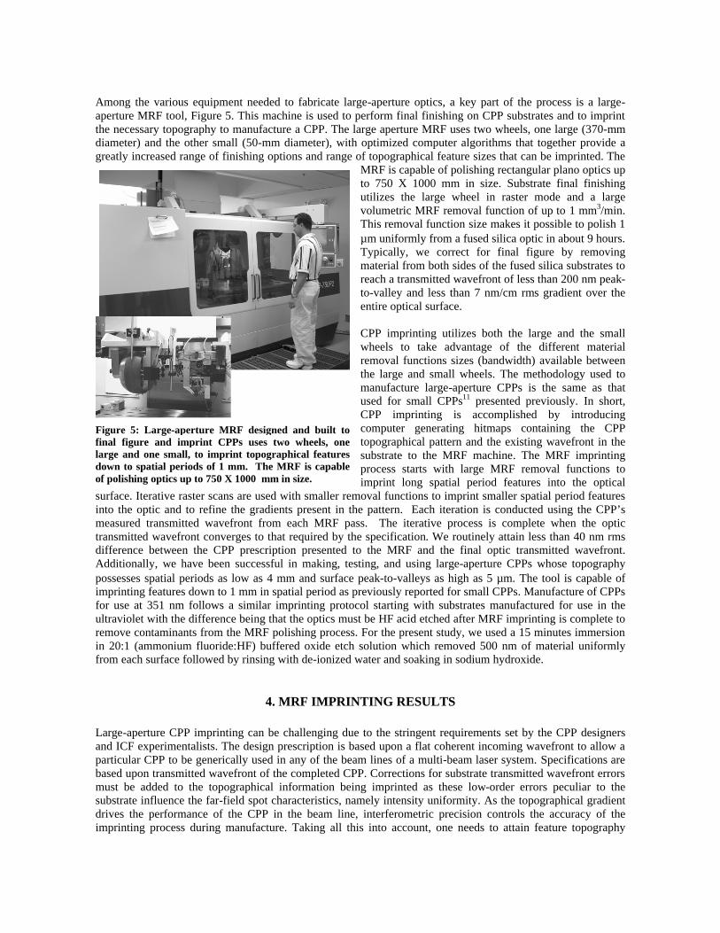
Among the various equipment needed to fabricate large-aperture optics, a key part of the process is a large-aperture MRF tool, Figure 5. This machine is used to perform final finishing on CPP substrates and to imprint the necessary topography to manufacture a CPP. The large aperture MRF uses two wheels, one large (370-mm diameter) and the other small (50-mm diameter), with optimized computer algorithms that together provide a greatly increased range of finishing options and range of topographical feature sizes that can be imprinted. The
MRF is capable of polishing rectangular plano optics up to 750 X 1000 mm in size. Substrate final finishing utilizes the large wheel in raster mode and a large volumetric MRF removal function of up to 1 mm3/min. This removal function size makes it possible to polish 1 µm uniformly from a fused silica optic in about 9 hours. Typically, we correct for final figure by removing material from both sides of the fused silica substrates to reach a transmitted wavefront of less than 200 nm peak-to-valley and less than 7 nm/cm rms gradient over the entire optical surface. CPP imprinting utilizes both the large and the small wheels to take advantage of the different material removal functions sizes (bandwidth) available between the large and small wheels. The methodology used to manufacture large-aperture CPPs is the same as that used for small CPPs11 presented previously. In short, CPP imprinting is accomplished by introducing computer generating hitmaps containing the CPP topographical pattern and the existing wavefront in the substrate to the MRF machine. The MRF imprinting process starts with large MRF removal functions to imprint long spatial period features into the optical
surface. Iterative raster scans are used with smaller removal functions to imprint smaller spatial period features into the optic and to refine the gradients present in the pattern. Each iteration is conducted using the CPP’s measured transmitted wavefront from each MRF pass. The iterative process is complete when the optic transmitted wavefront converges to that required by the specification. We routinely attain less than 40 nm rms difference between the CPP prescription presented to the MRF and the final optic transmitted wavefront. Additionally, we have been successful in making, testing, and using large-aperture CPPs whose topography possesses spatial periods as low as 4 mm and surface peak-to-valleys as high as 5 µm. The tool is capable of imprinting features down to 1 mm in spatial period as previously reported for small CPPs. Manufacture of CPPs for use at 351 nm follows a similar imprinting protocol starting with substrates manufactured for use in the ultraviolet with the difference being that the optics must be HF acid etched after MRF imprinting is complete to remove contaminants from the MRF polishing process. For the present study, we used a 15 minutes immersion in 20:1 (ammonium fluoride:HF) buffered oxide etch solution which removed 500 nm of material uniformly from each surface followed by rinsing with de-ionized water and soaking in sodium hydroxide.
4. MRF IMPRINTING RESULTS Large-aperture CPP imprinting can be challenging due to the stringent requirements set by the CPP designers and ICF experimentalists. The design prescription is based upon a flat coherent incoming wavefront to allow a particular CPP to be generically used in any of the beam lines of a multi-beam laser system. Specifications are based upon transmitted wavefront of the completed CPP. Corrections for substrate transmitted wavefront errors must be added to the topographical information being imprinted as these low-order errors peculiar to the substrate influence the far-field spot characteristics, namely intensity uniformity. As the topographical gradient drives the performance of the CPP in the beam line, interferometric precision controls the accuracy of the imprinting process during manufacture. Taking all this into account, one needs to attain feature topography
Figure 5: Large-aperture MRF designed and built to final figure and imprint CPPs uses two wheels, one large and one small, to imprint topographical features down to spatial periods of 1 mm. The MRF is capable of polishing optics up to 750 X 1000 mm in size.

transmitted wavefront differences with respect to the design prescription of less than 40 nm rms. In addition to the topographical feature accuracy, localized artifacts such as digs, scratches, sleeks, and surface contamination need to be controlled (virtually non-existent), especially for CPPs used in the ultraviolet. Even when used in the infrared at high fluences, these imperfections can lead to laser-induced damage on the CPP itself or fratricide on downstream optics due to contrast modulation. Figure 6 and Table 2 present the imprinting results for a CPP 702173 manufactured using the advanced finishing protocols discussed above for high-power laser applications at 351 nm compared to specification. The CPP topographical imprint meets specification after HF acid etching with no apparent change in parameters.
Table 2: Measured CPP 702173 performance parameters versus specification for a large-aperture NIF-CPP manufactured and tested at 351 nm, 3 nsec equivalent using MRF
Specification Measured Pass/Fail 80% Encircled Energy Radius (µm) 407.0 +/- 15.0 395.0 PASS 90% Encircled Energy Radius (µm) 460.0 +/- 15.0 452.7 PASS 95% Encircled Energy Radius (µm) 505.0 +/- 15.0 502.1 PASS
Individual Lineout RMS Deviation (%) 5.0 3.2 PASS 2D RMS Deviation over Central Area (%) 5.0 2.9 PASS 50 % Eccentricity (a = 396.1, b = 212.2) 0.53 +/- 0.1 0.53 PASS
Figure 6: CPP 702173 imprinting results and far-field spot characteristics. Top left – near-field topographical pattern imprinted using MRF. Top right – far-field spot encircled energy radius. Bottom left – far-field spot intensity contour map. Bottom right – far-field spot line-outs taken at 0, 45, 90 and 135 degrees.
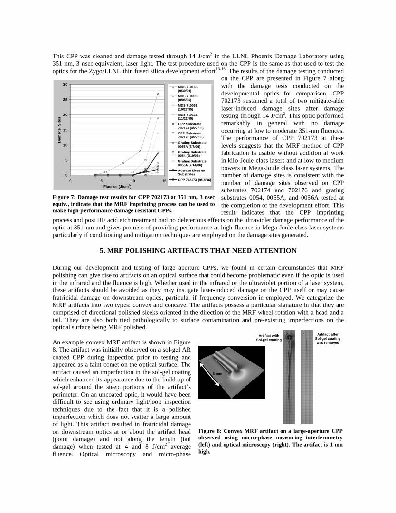
This CPP was cleaned and damage tested through 14 J/cm2 in the LLNL Phoenix Damage Laboratory using 351-nm, 3-nsec equivalent, laser light. The test procedure used on the CPP is the same as that used to test the optics for the Zygo/LLNL thin fused silica development effort13-16. The results of the damage testing conducted
on the CPP are presented in Figure 7 along with the damage tests conducted on the developmental optics for comparison. CPP 702173 sustained a total of two mitigate-able laser-induced damage sites after damage testing through 14 J/cm2. This optic performed remarkably in general with no damage occurring at low to moderate 351-nm fluences. The performance of CPP 702173 at these levels suggests that the MRF method of CPP fabrication is usable without addition al work in kilo-Joule class lasers and at low to medium powers in Mega-Joule class laser systems. The number of damage sites is consistent with the number of damage sites observed on CPP substrates 702174 and 702176 and grating substrates 0054, 0055A, and 0056A tested at the completion of the development effort. This result indicates that the CPP imprinting
process and post HF acid etch treatment had no deleterious effects on the ultraviolet damage performance of the optic at 351 nm and gives promise of providing performance at high fluence in Mega-Joule class laser systems particularly if conditioning and mitigation techniques are employed on the damage sites generated.
5. MRF POLISHING ARTIFACTS THAT NEED ATTENTION During our development and testing of large aperture CPPs, we found in certain circumstances that MRF polishing can give rise to artifacts on an optical surface that could become problematic even if the optic is used in the infrared and the fluence is high. Whether used in the infrared or the ultraviolet portion of a laser system, these artifacts should be avoided as they may instigate laser-induced damage on the CPP itself or may cause fratricidal damage on downstream optics, particular if frequency conversion in employed. We categorize the MRF artifacts into two types: convex and concave. The artifacts possess a particular signature in that they are comprised of directional polished sleeks oriented in the direction of the MRF wheel rotation with a head and a tail. They are also both tied pathologically to surface contamination and pre-existing imperfections on the optical surface being MRF polished. An example convex MRF artifact is shown in Figure 8. The artifact was initially observed on a sol-gel AR coated CPP during inspection prior to testing and appeared as a faint comet on the optical surface. The artifact caused an imperfection in the sol-gel coating which enhanced its appearance due to the build up of sol-gel around the steep portions of the artifact’s perimeter. On an uncoated optic, it would have been difficult to see using ordinary light/loop inspection techniques due to the fact that it is a polished imperfection which does not scatter a large amount of light. This artifact resulted in fratricidal damage on downstream optics at or about the artifact head (point damage) and not along the length (tail damage) when tested at 4 and 8 J/cm2 average fluence. Optical microscopy and micro-phase
0
5
10
15
20
25
30
0 5 10 15Fluence (J/cm2)
Dam
age
Sit
es
MDS 710163(9/30/04)
MDS 710096(8/05/05)
MDS 710053(10/27/05)
MDS 710122(11/22/05)
CPP Substrate702174 (4/27/06)
CPP Substrate702176 (4/27/06)
Grating Substrate0055A (7/7/06)
Grating Substrate0054 (7/19/06)
Grating Substrate0056A (7/14/06)
Average Sites onSubstrates
CPP 702173 (9/18/06)
Figure 7: Damage test results for CPP 702173 at 351 nm, 3 nsec equiv., indicate that the MRF imprinting process can be used to make high-performance damage resistant CPPs.
Artifact with Sol-gel coating
Artifact after Sol-gel coating was removed
3 mm
Figure 8: Convex MRF artifact on a large-aperture CPP observed using micro-phase measuring interferometry (left) and optical microscopy (right). The artifact is 1 µm high.
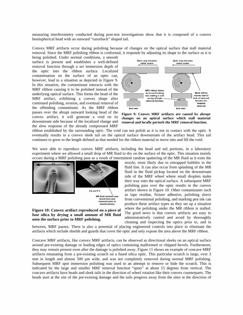
measuring interferometry conducted during post-test investigations show that it is composed of a convex hemispherical head with an outward “razorback” shaped tail. Convex MRF artifacts occur during polishing because of changes on the optical surface that stall material removal. Since the MRF polishing ribbon is conformal, it responds by adjusting its shape to the surface as it is being polished. Under normal conditions, a smooth surface is present and establishes a well-defined removal function through a set immersion depth of the optic into the ribbon surface. Localized contamination on the surface of an optic can, however, lead to a situation as depicted in Figure 9. In this situation, the contaminant interacts with the MRF ribbon causing it to be polished instead of the underlying optical surface. This forms the head of the MRF artifact, exhibiting a convex shape after continued polishing, erosion, and eventual removal of the offending contaminant. As the MRF ribbon passes over the abrupt outward looking head of the convex artifact, it will generate a void on its downstream side because of the localized change and the slow response of the already compressed MRF ribbon established by the surrounding optic. The void can not polish as it is not in contact with the optic. It eventually results in a convex sleek tail on the optical surface downstream of the artifact head. This tail continues to grow to the length defined as that needed for the ribbon material to move into and fill the void. We were able to reproduce convex MRF artifacts, including the head and tail portions, in a laboratory experiment where we allowed a small drop of MR fluid to dry on the surface of the optic. This situation mainly occurs during a MRF polishing pass as a result of intermittent random spattering of the MR fluid as it exits the
nozzle, most likely due to entrapped bubbles in the fluid line. It can also occur from splashing of the MR fluid in the fluid pickup located on the downstream side of the MRF wheel where small droplets make their way onto the optical surface. A subsequent MRF polishing pass over the optic results in the convex artifact shown in Figure 10. Other contaminants such as tape residue, fixture adhesive, polishing slurry from conventional polishing, and marking pen ink can produce these artifact types as they set up a situation where the polishing under the MR ribbon is stalled. The good news is that convex artifacts are easy to administratively control and avoid by thoroughly cleaning and inspecting the optics prior to, and in
between, MRF passes. There is also a potential of placing engineered controls into place to eliminate the artifacts which include shields and guards that cover the optic and only expose the area above the MRF ribbon. Concave MRF artifacts, like convex MRF artifacts, can be observed as directional sleeks on an optical surface around pre-existing damage or leading edges of optics containing malformed or chipped bevels. Furthermore, they may remain present even after the damage is polished away. Figure 11 shows an example of concave MRF artifacts emanating from a pre-existing scratch on a fused silica optic. This particular scratch is large, over 3 mm in length and almost 500 µm wide, and was not completely removed during normal MRF polishing. Subsequent MRF spot immersion polishing was used in an attempt to remove or hide the scratch. This is indicated by the large and smaller MRF removal function “spots” at about 15 degrees from vertical. The concave artifacts have heads and sleek tails in the direction of wheel rotation like their convex counterparts. The heads start at the site of the pre-existing damage and the tails progress away from the sites in the direction of
Figure 9: Convex MRF artifacts are caused by abrupt changes on an optical surface which stall material removal and locally perturb the MRF removal function.
0.5 mm
3.6 µm P-V
MR fluid remnant was found here and
removed prior to interferometry
Figure 10: Convex artifact reproduced on a piece of fuse silica by drying a small amount of MR fluid onto the surface prior to MRF polishing.
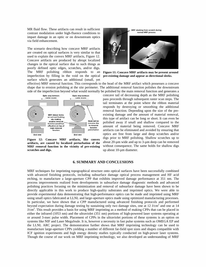
MR fluid flow. These artifacts can result in sufficient contrast modulation under high-fluence conditions to impart damage in an optic or on downstream optics via field enhancement. The scenario describing how concave MRF artifacts are created on optical surfaces is very similar to that used to explain the convex MRF artifacts, Figure 12. Concave artifacts are produced by abrupt localized changes in the optical surface due to such things as poorly defined optic edges, scratches, and/or digs. The MRF polishing ribbon responds to an imperfection by filling in the void on the optical surface which generates an additional (small, yet effective) MRF removal function. This corresponds to the head of the MRF artifact which possesses a concave shape due to erosion polishing at the site perimeter. The additional removal function polishes the downstream side of the imperfection beyond what would normally be polished by the main removal function and generates a
concave tail of decreasing depth as the MRF polishing pass proceeds through subsequent raster scan steps. The tail terminates at the point where the ribbon material responds by destroying or smoothing the additional removal function. Depending upon the size of the pre-existing damage and the amount of material removal, this type of artifact can be long or short. It can even be polished away if small and shallow compared to the amount of material being removed. Concave MRF artifacts can be eliminated and avoided by ensuring that optics are free from large and deep scratches and/or digs prior to MRF polishing. Shallow scratches up to about 20-µm wide and up to 3-µm deep can be removed without consequence. The same holds for shallow digs up about 10-µm diameter.
6. SUMMARY AND CONCLUSIONS MRF techniques for imprinting topographical structure onto optical surfaces have been successfully combined with advanced finishing protocols, including subsurface damage optical process management and HF acid etching, to manufacture a large-aperture CPP that exhibits improved damage performance at 351 nm. The process improvements realized from developments in subsurface damage diagnostic methods and advanced polishing practices focusing on the minimization and removal of subsurface damage have been shown to be directly applicable in this work to produce high-quality substrates and imprinted optics. We were able to provide experimental data demonstrating that high-performance optics can be made and imprinted using MRF using small optics fabricated at LLNL and large-aperture optics made using optimized manufacturing processes. In particular, we have shown that a CPP manufactured using advanced finishing protocols and performed beyond expectation during damage testing by sustaining only two damage sites, one at 12 J/cm2 and one at 14 J/cm2. This result provides a basis for using MRF imprinting as a method of making CPPs that can be placed in either the infrared (1053 nm) and the ultraviolet (351 nm) portions of high-powered laser systems operating at or around 3-nsec pulse width. Placement of CPPs in the ultraviolet portions of these systems is an option on systems like NIF and Laser MegaJoule. It is, however a necessity in fast pulse systems such as OMEGA EP and the LLNL ARC project. The demonstration further shows that MRF imprinting technology can be used to manufacture large-aperture CPPs yielding a number of different far-field spot sizes and shapes compatible with ICF ignition experiments and high energy density studies typically conducted on high-power laser systems. Though the course of our work on MRF imprinting technology, we also developed an understanding of MRF
Figure 12: Concave MRF artifacts, like convexartifacts, are caused by localized perturbation of the MRF removal function in the vicinity of pre-existing scratches and digs.
3 mm
MRF sleeking from scratch during normal MRF process
Spot sleek direction
Figure 11: Concave MRF artifacts may be present around pre-existing damage and appear as directional sleeks.

related polishing artifacts that could potentially cause problems if not addressed regardless of the use wavelength. We are able to categorize and attribute convex and concave type MRF polishing artifacts through the study of manufactured optics and through their reproduction in the laboratory. We are also able to explain their origin and suggest methods to minimize or avoid them on MRF finished optics.
REFERENCES 1. J. Paisner and J.R. Murray. Overview of the National Ignition Facility Project. Proc. SPIE Conf. Solid-State
Laser Apps. To ICF (Monterey, CA 1998). 2. P. Wegner, J. Auerbach, T. Biediada, S. Dixit, J. Lawson, J. Menapace, T. Parham, D. Swift, P. Whitman,
and W. Williams. NIF final optics system: frequency conversion and beam conditioning. Proceedings of the SPIE, Volume 5341, pp. 180-189 (2004).
3. S.N. Dixit, M.D. Feit, M.D. Perry, and H.T. Powell. Designing fully continuous phase screens for tailoring focal-plane irradiance profiles. Optics Letters, vol. 21, no. 21, 1 Nov. 1996, pp. 1715-1717.
4. B.W Woods, I.M. Thomas, M.A. Henessian, S.N. Dixit, H.T. Powell. Large-aperture (80-cm diameter) phase plates for beam smoothing on Nova. Solid State Lasers II, G.Dube, ed., Proc. SPIE 1410, pp. 47-54 (1991).
5. S.N. Dixit, I.M. Thomas, B.W Woods, A.J. Morgan, M.A. Henessian, P.J. Wegner, and H.T Powell. Random phase plates for beam smoothing on the Nova laser. Applied Optics, 32, 2543-2554 (1993).
6. I.M. Thomas, S.N. Dixit, and M.C. Rushford. Kinoform phase plates for focal plane irradiance profile control. Optics Letters, vol. 19, pp. 417-419 (1994).
7. I.M. Thomas, S.N. Dixit, and M.C. Rushford. Preparation of random phase plates for laser beam smoothing. Laser Induced Damage in Optical Materials: 1994 H.E. Bennett A.H. Guenther, M.R. Kozlowski, B.E. Newman and M.J. Soileau, eds., Proc. SPIE 2428, pp. 264-270 (1994).
8. Distributed phase plates for super-Gaussian focal plane irradiance profiles. LLE (Laboratory for Laser Energetics) Rev. 63, pp. 126-129 (1995).
9. A High-Pass Phase Plate Design for OMEGA and the NIF. LLE (Laboratory for Laser Energetics) Rev. 89, pp. 11-24 (2001).
10. Jerome Neauport, Xavier Ribeyre, Jerome Daurios, Denis Valla, Martine Lavergne, Vincent Beau, and Laurent Videau. Design and optical characterization of a large continuous phase plate for Laser Integration Line and laser Megajoule facilities. Applied Optics, vol. 42, no. 13, 1 May 2003, pp. 2377-2383.
11. J. A. Menapace, S. N. Dixit, Francois Y. Génin, and W. F. Brocious, “Magnetorheological Finishing for Imprinting Continuous Phase Plate Structure onto Optical Surfaces”, Laser Induced Damage in Optical Materials, SPIE Proc., 5273, 220-230 (2003).
12. Joseph A. Menapace, Bernie Penetrante, Don Golini, Al Slomba, Phil E. Miller, Tom Parham, Mike Nichols, and John Peterson. Combined advanced finishing and UV-laser conditioning for producing UV-damage-resistant fused silica optics. Laser Induced Damage in Optical Materials: Proc. SPIE, 4679, pp. 56-68 (2002).
13. P. E. Miller, T. I. Suratwala, J. P. Menapace, L. L. Wong, P. J. Davis, and W. A. Steele, “The Distribution of Subsurface Damage in Fused Silica” Laser Induced Damage in Optical Materials, SPIE Proc., 5991, 599101 1-25 (2005).
14. T. Suratwala, L. Wong, P. Miller, M. D. Feit, J. Menapace, R. Steele, P. Davis, D. Walmer, “Sub-surface mechanical damage distributions during grinding of fused silica”, Journal of the American Ceramics Society, in submission.
15. J. A. Menapace, P. J. Davis, W. A. Steele, L. L. Wong, T. I. Suratwala, and P. E. Miller, “MRF Applications: Measurement of Process-dependent Subsurface Damage in Optical Materials using the MRF Wedge Technique”, Laser Induced Damage in Optical Materials SPIE Proc., 5991, 599103 1-9 (2005).
16. J. A. Menapace, P. J. Davis, W. A. Steele, L. L. Wong, T. I. Suratwala, and P. E. Miller, “Utilization of Magnetorheological Finishing as a Diagnostic Tool for Investigating the Three-Dimensional Structure of Fractures in Fused Silica”, Laser Induced Damage in Optical Materials SPIE Proc., 5991, 599102 1-13 (2005).