Embed Size (px)
Citation preview
InvenSense Inc. 1745 Technology Drive, San Jose, CA 95110 U.S.A
+1(408) 988–7339 www.invensense.com
Document Number: PS-MPU-6881A-00 Revision: 1.0 Release Date: 05/22/2014
1 of 38
MPU-6881
Product Specification
Revision 1.0
MPU-6881 Product Specification Document Number: PS-MPU-6881A-00 Revision: 1.0 Release Date: 05/22/2014
2 of 38
TABLE OF CONTENTS
TABLE OF FIGURES ......................................................................................................................................... 4
TABLE OF TABLES .......................................................................................................................................... 5
1 DOCUMENT INFORMATION ...................................................................................................................... 6
1.1 REVISION HISTORY .............................................................................................................................. 6
1.2 PURPOSE AND SCOPE .......................................................................................................................... 7
1.3 PRODUCT OVERVIEW ........................................................................................................................... 7
1.4 APPLICATIONS ..................................................................................................................................... 7
2 FEATURES .................................................................................................................................................. 8
2.1 GYROSCOPE FEATURES ....................................................................................................................... 8
2.2 ACCELEROMETER FEATURES ............................................................................................................... 8
2.3 ADDITIONAL FEATURES ........................................................................................................................ 8
3 ELECTRICAL CHARACTERISTICS ........................................................................................................... 9
3.1 GYROSCOPE SPECIFICATIONS .............................................................................................................. 9
3.2 ACCELEROMETER SPECIFICATIONS ..................................................................................................... 10
3.3 ELECTRICAL SPECIFICATIONS ............................................................................................................. 11
3.4 I2C TIMING CHARACTERIZATION ......................................................................................................... 15
3.5 SPI TIMING CHARACTERIZATION ......................................................................................................... 16
3.6 ABSOLUTE MAXIMUM RATINGS ........................................................................................................... 18
4 APPLICATIONS INFORMATION .............................................................................................................. 19
4.1 PIN OUT DIAGRAM AND SIGNAL DESCRIPTION ..................................................................................... 19
4.2 TYPICAL OPERATING CIRCUIT ............................................................................................................. 20
4.3 BILL OF MATERIALS FOR EXTERNAL COMPONENTS .............................................................................. 20
4.4 BLOCK DIAGRAM ............................................................................................................................... 21
4.5 OVERVIEW ........................................................................................................................................ 21
4.6 THREE-AXIS MEMS GYROSCOPE WITH 16-BIT ADCS AND SIGNAL CONDITIONING ................................ 22
4.7 THREE-AXIS MEMS ACCELEROMETER WITH 16-BIT ADCS AND SIGNAL CONDITIONING ........................ 22
4.8 I2C AND SPI SERIAL COMMUNICATIONS INTERFACES .......................................................................... 22
4.9 SELF-TEST ........................................................................................................................................ 24
4.10 CLOCKING ......................................................................................................................................... 25
4.11 SENSOR DATA REGISTERS ................................................................................................................. 25
4.12 FIFO ................................................................................................................................................ 25
4.13 INTERRUPTS ...................................................................................................................................... 25
4.14 DIGITAL-OUTPUT TEMPERATURE SENSOR .......................................................................................... 25

MPU-6881 Product Specification Document Number: PS-MPU-6881A-00 Revision: 1.0 Release Date: 05/22/2014
3 of 38
4.15 BIAS AND LDOS ................................................................................................................................ 26
4.16 CHARGE PUMP .................................................................................................................................. 26
4.17 STANDARD POWER MODES ................................................................................................................ 26
5 PROGRAMMABLE INTERRUPTS ............................................................................................................ 27
6 DIGITAL INTERFACE ............................................................................................................................... 28
6.1 I2C AND SPI SERIAL INTERFACES ...................................................................................................... 28
6.2 I2C INTERFACE .................................................................................................................................. 28
6.3 I2C COMMUNICATIONS PROTOCOL ..................................................................................................... 28
6.4 I2C TERMS ........................................................................................................................................ 31
6.5 SPI INTERFACE ................................................................................................................................. 32
7 SERIAL INTERFACE CONSIDERATIONS ............................................................................................... 32
7.1 MPU-6881 SUPPORTED INTERFACES ................................................................................................. 33
8 ASSEMBLY ............................................................................................................................................... 34
8.1 ORIENTATION OF AXES ...................................................................................................................... 34
8.2 PACKAGE DIMENSIONS ...................................................................................................................... 35
9 PART NUMBER PACKAGE MARKING ................................................................................................... 36
10 RELIABILITY ............................................................................................................................................. 37
10.1 QUALIFICATION TEST POLICY ............................................................................................................. 37
10.2 QUALIFICATION TEST PLAN ................................................................................................................ 37
11 REFERENCE ............................................................................................................................................. 38

MPU-6881 Product Specification Document Number: PS-MPU-6881A-00 Revision: 1.0 Release Date: 05/22/2014
4 of 38
Table of Figures
Figure 1 I2C Bus Timing Diagram .................................................................................................................... 15 Figure 2 SPI Bus Timing Diagram .................................................................................................................... 16 Figure 3 Pin out Diagram for MPU-6881 3.0x3.0x0.9mm QFN ........................................................................ 19 Figure 4 MPU-6881 QFN Application Schematic. (a) I2C operation, (b) SPI operation. ................................ 20 Figure 5 MPU-6881 Block Diagram .................................................................................................................. 21 Figure 6 MPU-6881 Solution Using I2C Interface ............................................................................................ 23 Figure 7 MPU-6881 Solution Using SPI Interface ............................................................................................ 24 Figure 8 START and STOP Conditions ............................................................................................................ 29 Figure 9 Acknowledge on the I2C Bus .............................................................................................................. 29 Figure 10 Complete I2C Data Transfer ............................................................................................................. 30 Figure 11 Typical SPI Master / Slave Configuration ......................................................................................... 32 Figure 12 I/O Levels and Connections ............................................................................................................. 33 Figure 13 Orientation of Axes Sensitivity and Polarity of Rotation ................................................................... 34

MPU-6881 Product Specification Document Number: PS-MPU-6881A-00 Revision: 1.0 Release Date: 05/22/2014
5 of 38
Table of Tables Table 1 Gyroscope Specifications ...................................................................................................................... 9 Table 2 Accelerometer Specifications .............................................................................................................. 10 Table 3 D.C. Electrical Characteristics ............................................................................................................. 11 Table 4 A.C. Electrical Characteristics ............................................................................................................. 13 Table 5 Other Electrical Specifications ............................................................................................................. 14 Table 6 I2C Timing Characteristics ................................................................................................................... 15 Table 7 SPI Timing Characteristics .................................................................................................................. 16 Table 8 fCLK = 20MHz ..................................................................................................................................... 17 Table 9 Absolute Maximum Ratings ................................................................................................................. 18 Table 10 Signal Descriptions ............................................................................................................................ 19 Table 11 Bill of Materials .................................................................................................................................. 20 Table 12 Standard Power Modes for MPU-6881.............................................................................................. 26 Table 13 Table of Interrupt Sources ................................................................................................................. 27 Table 14 Serial Interface ................................................................................................................................... 28 Table 15 I2C Terms ........................................................................................................................................... 31

MPU-6881 Product Specification Document Number: PS-MPU-6881A-00 Revision: 1.0 Release Date: 05/22/2014
6 of 38
1 Document Information
1.1 Revision History
Revision Date
Revision Description
05/22/2014 1.0 Initial Release

MPU-6881 Product Specification Document Number: PS-MPU-6881A-00 Revision: 1.0 Release Date: 05/22/2014
7 of 38
1.2 Purpose and Scope This document is a preliminary product specification, providing a description, specifications, and design related information on the MPU-6881™ MotionTracking device. The device is housed in a small 3x3x0.9mm 24-pin QFN package.
Specifications are subject to change without notice. Final specifications will be updated based upon characterization of production silicon. For references to register map and descriptions of individual registers, please refer to the MPU-6881 Register Map and Register Descriptions document.
1.3 Product Overview The MPU-6881 is a 6-axis MotionTracking device that combines a 3-axis gyroscope, and a 3-axis accelerometer in a small 3x3x0.9mm (24-pin QFN) package. It also features a 4096-byte FIFO that can lower the traffic on the serial bus interface, and reduce power consumption by allowing the system processor to burst read sensor data and then go into a low-power mode. With its dedicated I2C sensor bus, the MPU-6881 directly accepts inputs from external I2C devices. MPU-6881, with its 6-axis integration, enables manufacturers to eliminate the costly and complex selection, qualification, and system level integration of discrete devices, guaranteeing optimal motion performance for consumers. MPU-6881 is also designed to interface with multiple non-inertial digital sensors, such as pressure sensors, on its auxiliary I2C port.
The gyroscope has a programmable full-scale range of ±250, ±500, ±1000, and ±2000 degrees/sec. The accelerometer has a user-programmable accelerometer full-scale range of ±2g, ±4g, ±8g, and ±16g. Factory-calibrated initial sensitivity of both sensors reduces production-line calibration requirements.
Other industry-leading features include on-chip 16-bit ADCs, programmable digital filters, a precision clock with 1% drift from -40°C to 85°C, an embedded temperature sensor, and programmable interrupts. The device features I2C and SPI serial interfaces, a VDD operating range of 1.71 to 3.45V, and a separate digital IO supply, VDDIO from 1.71V to 3.45V.
Communication with all registers of the device is performed using either I2C at 400kHz or SPI at 1MHz. For applications requiring faster communications, the sensor and interrupt registers may be read using SPI at 20MHz.
By leveraging its patented and volume-proven CMOS-MEMS Fabrication platform, which integrates MEMS wafers with companion CMOS electronics through wafer-level bonding, InvenSense has driven the package size down to a footprint and thickness of 3x3x0.9mm (24-pin QFN), to provide a very small yet high performance low cost package. The device provides high robustness by supporting 10,000g shock reliability.
1.4 Applications
TouchAnywhere™ technology (for “no touch” UI Application Control/Navigation) MotionCommand™ technology (for Gesture Short-cuts) Motion-enabled game and application framework Location based services, points of interest, and dead reckoning Handset and portable gaming Motion-based game controllers 3D remote controls for Internet connected DTVs and set top boxes, 3D mice Wearable sensors for health, fitness and sports

MPU-6881 Product Specification Document Number: PS-MPU-6881A-00 Revision: 1.0 Release Date: 05/22/2014
8 of 38
2 Features
2.1 Gyroscope Features The triple-axis MEMS gyroscope in the MPU-6881 includes a wide range of features:
Digital-output X-, Y-, and Z-axis angular rate sensors (gyroscopes) with a user-programmable full-scale range of ±250, ±500, ±1000, and ±2000°/sec and integrated 16-bit ADCs
Digitally-programmable low-pass filter Gyroscope operating current: 3.2mA Factory calibrated sensitivity scale factor Self-test
2.2 Accelerometer Features The triple-axis MEMS accelerometer in MPU-6881 includes a wide range of features:
Digital-output X-, Y-, and Z-axis accelerometer with a programmable full scale range of ±2g, ±4g, ±8g and ±16g and integrated 16-bit ADCs
Accelerometer normal operating current: 450µA Low power accelerometer mode current: 7.27µA at 0.98Hz, 18.65µA at 31.25Hz User-programmable interrupts Wake-on-motion interrupt for low power operation of applications processor Self-test
2.3 Additional Features The MPU-6881 includes the following additional features:
Auxiliary master I2C bus for reading data from external sensors (e.g. magnetometer) 3.4mA operating current when all 6 motion sensing axes are active VDD supply voltage range of 1.8 – 3.3V ± 5% VDDIO reference voltage of 1.8 – 3.3V ± 5% for auxiliary I2C devices Smallest and thinnest QFN package for portable devices: 3x3x0.9mm (24-pin QFN) Minimal cross-axis sensitivity between the accelerometer and gyroscope axes 4096 byte FIFO buffer enables the applications processor to read the data in bursts Digital-output temperature sensor User-programmable digital filters for gyroscope, accelerometer, and temp sensor 10,000 g shock tolerant 400kHz Fast Mode I2C for communicating with all registers 1MHz SPI serial interface for communicating with all registers 20MHz SPI serial interface for reading sensor and interrupt registers MEMS structure hermetically sealed and bonded at wafer level RoHS and Green compliant
MPU-6881 Product Specification Document Number: PS-MPU-6881A-00 Revision: 1.0 Release Date: 05/22/2014
9 of 38
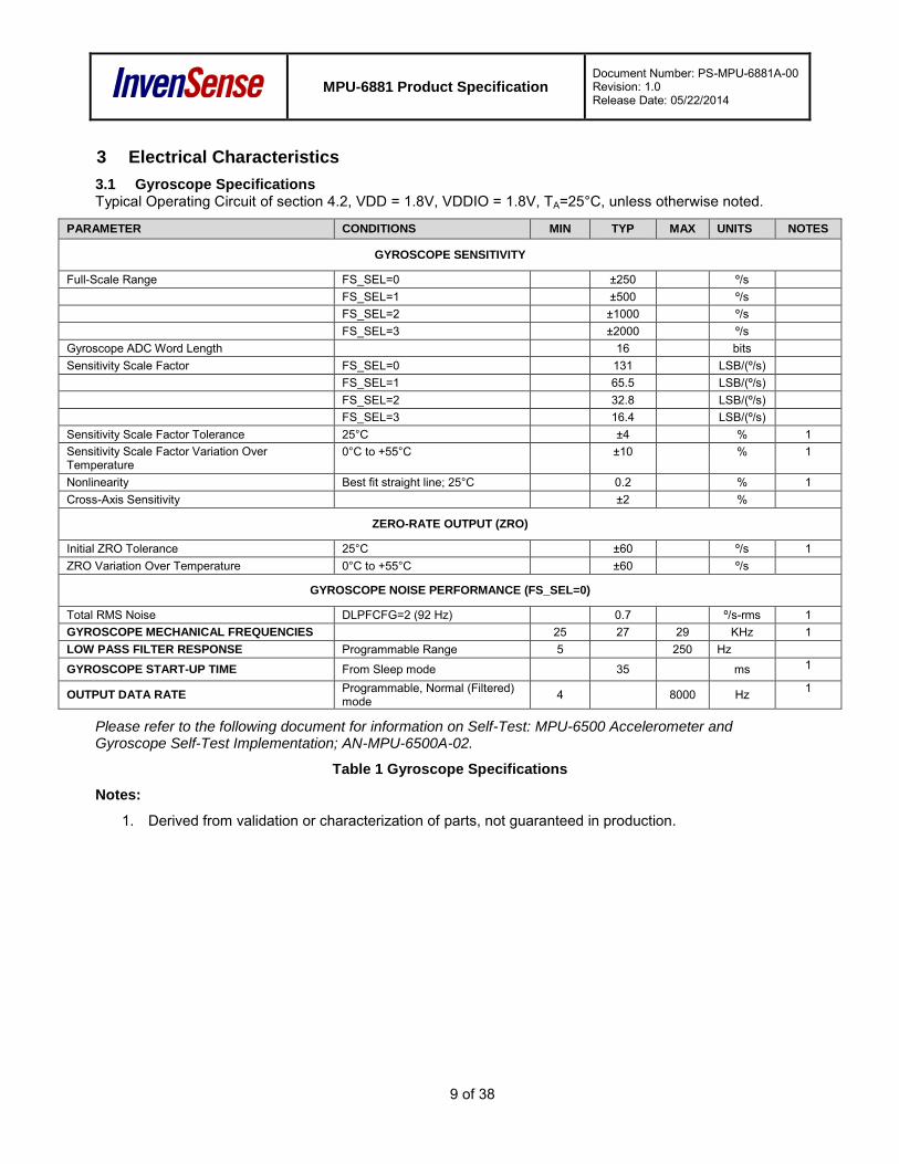
3 Electrical Characteristics
3.1 Gyroscope Specifications Typical Operating Circuit of section 4.2, VDD = 1.8V, VDDIO = 1.8V, TA=25°C, unless otherwise noted.
PARAMETER CONDITIONS MIN TYP MAX UNITS NOTES
GYROSCOPE SENSITIVITY
Full-Scale Range FS_SEL=0 ±250 º/s FS_SEL=1 ±500 º/s FS_SEL=2 ±1000 º/s FS_SEL=3 ±2000 º/s Gyroscope ADC Word Length 16 bits Sensitivity Scale Factor FS_SEL=0 131 LSB/(º/s) FS_SEL=1 65.5 LSB/(º/s) FS_SEL=2 32.8 LSB/(º/s) FS_SEL=3 16.4 LSB/(º/s) Sensitivity Scale Factor Tolerance 25°C ±4 % 1 Sensitivity Scale Factor Variation Over Temperature
0°C to +55°C ±10 % 1
Nonlinearity Best fit straight line; 25°C 0.2 % 1 Cross-Axis Sensitivity ±2 %
ZERO-RATE OUTPUT (ZRO)
Initial ZRO Tolerance 25°C ±60 º/s 1 ZRO Variation Over Temperature 0°C to +55°C ±60 º/s
GYROSCOPE NOISE PERFORMANCE (FS_SEL=0)
Total RMS Noise DLPFCFG=2 (92 Hz) 0.7 º/s-rms 1 GYROSCOPE MECHANICAL FREQUENCIES 25 27 29 KHz 1 LOW PASS FILTER RESPONSE Programmable Range 5 250 Hz
GYROSCOPE START-UP TIME From Sleep mode 35 ms 1
OUTPUT DATA RATE Programmable, Normal (Filtered) mode 4 8000 Hz 1
Please refer to the following document for information on Self-Test: MPU-6500 Accelerometer and Gyroscope Self-Test Implementation; AN-MPU-6500A-02.
Table 1 Gyroscope Specifications
Notes:
1. Derived from validation or characterization of parts, not guaranteed in production.

MPU-6881 Product Specification Document Number: PS-MPU-6881A-00 Revision: 1.0 Release Date: 05/22/2014
10 of 38
3.2 Accelerometer Specifications Typical Operating Circuit of section 4.2, VDD = 1.8V, VDDIO = 1.8V, TA=25°C, unless otherwise noted.
PARAMETER CONDITIONS MIN TYP MAX UNITS NOTES
ACCELEROMETER SENSITIVITY
Full-Scale Range
AFS_SEL=0 ±2 g AFS_SEL=1 ±4 g AFS_SEL=2 ±8 g AFS_SEL=3 ±16 g
ADC Word Length Output in two’s complement format 16 bits
Sensitivity Scale Factor
AFS_SEL=0 16,384 LSB/g AFS_SEL=1 8,192 LSB/g AFS_SEL=2 4,096 LSB/g AFS_SEL=3 2,048 LSB/g
Initial Calibration Tolerance ±4 % 1
Sensitivity Change vs. Temperature -40°C to +85°C AFS_SEL=0 Component-level
±4 % 1
Nonlinearity Best Fit Straight Line 0.5 % Cross-Axis Sensitivity ±2 %
ZERO-G OUTPUT
Initial Tolerance Component-level, all axes -80 ±60 +80 mg
Zero-G Level Change vs. Temperature X and Y axes, 0°C to +70°C Z axis, 0°C to +70°C
-0.64 -1
+0.64 +1
mg/ºC
mg/ºC
NOISE PERFORMANCE
Power Spectral Density Low noise mode 400 µg/√Hz 1 LOW PASS FILTER RESPONSE Programmable Range 5 260 Hz INTELLIGENCE FUNCTION INCREMENT
32 mg/LSB
ACCELEROMETER STARTUP TIME From Sleep mode 20 ms From Cold Start, 1ms VDD ramp 30 ms
OUTPUT DATA RATE
Low power (duty-cycled) 0.244 500 Hz 1 Duty-cycled, over temp ±15 %
Low noise (active) 4 4000 Hz
Please refer to the following document for information on Self-Test: MPU-6500 Accelerometer and Gyroscope Self-Test Implementation; AN-MPU-6500A-02.
Table 2 Accelerometer Specifications
Notes:
1. Derived from validation or characterization of parts, not guaranteed in production.

MPU-6881 Product Specification Document Number: PS-MPU-6881A-00 Revision: 1.0 Release Date: 05/22/2014
11 of 38
3.3 Electrical Specifications
3.3.1 D.C. Electrical Characteristics
Typical Operating Circuit of section 4.2, VDD = 1.8V, VDDIO = 1.8V, TA=25°C, unless otherwise noted.
PARAMETER CONDITIONS MIN TYP MAX Units Notes
SUPPLY VOLTAGES
VDD 1.71 1.8 3.45 V
VDDIO 1.71 1.8 3.45 V
SUPPLY CURRENTS
Normal Mode 6-axis 3.4 mA 1
3-axis Gyroscope 3.2 mA 1
3-Axis Accelerometer 450 µA 1
Accelerometer Low Power Mode (Gyroscope disabled)
0.98 Hz update rate 7.27 µA 1,2
31.25 Hz update rate 18.65 µA 1,2
Standby Mode 1.6 mA 1 Full-Chip Sleep Mode 6 µA 1
TEMPERATURE RANGE
Specified Temperature Range Performance parameters are not applicable beyond Specified Temperature Range -40 +85 °C
Table 3 D.C. Electrical Characteristics
Notes:
1. Derived from validation or characterization of parts, not guaranteed in production. 2. Accelerometer Low Power Mode supports the following output data rates (ODRs): 0.24, 0.49, 0.98,
1.95, 3.91, 7.81, 15.63, 31.25, 62.50, 125, 250, 500Hz. Supply current for any update rate can be calculated as:
a. Supply Current in µA = 6.9 + Update Rate * 0.376

MPU-6881 Product Specification Document Number: PS-MPU-6881A-00 Revision: 1.0 Release Date: 05/22/2014
12 of 38
3.3.2 A.C. Electrical Characteristics
Typical Operating Circuit of section 4.2, VDD = 1.8V, VDDIO = 1.8V, TA=25°C, unless otherwise noted.
Parameter Conditions MIN TYP MAX Units NOTES
SUPPLIES
Supply Ramp Time Monotonic ramp. Ramp rate is 10% to 90% of the final value
0.1 100 ms
1
TEMPERATURE SENSOR
Operating Range Ambient -40 85 °C 1 Sensitivity Untrimmed 333.87 LSB/°C
Room Temp Offset 21°C 0 LSB
Power-On RESET
Supply Ramp Time (TRAMP) Valid power-on RESET 0.01 20 100 ms 1
Start-up time for register read/write From power-up 11 100 ms 1
I2C ADDRESS AD0 = 0
AD0 = 1 1101000 1101001
DIGITAL INPUTS (SYNC, AD0, SCLK, SDI, CS)
VIH, High Level Input Voltage 0.7*VDDIO V 1 VIL, Low Level Input Voltage 0.3*VDDIO V
CI, Input Capacitance < 10 pF
DIGITAL OUTPUT (SDO, INT)
VOH, High Level Output Voltage RLOAD=1MΩ; 0.9*VDDIO V
1
VOL1, LOW-Level Output Voltage RLOAD=1MΩ; 0.1*VDDIO V VOL.INT1, INT Low-Level Output Voltage OPEN=1, 0.3mA sink
Current 0.1 V
Output Leakage Current OPEN=1 100 nA tINT, INT Pulse Width LATCH_INT_EN=0 50 µs
I2C I/O (SCL, SDA)
VIL, LOW Level Input Voltage -0.5V 0.3*VDDIO V
1
VIH, HIGH-Level Input Voltage 0.7*VDDIO VDDIO + 0.5V
V
Vhys, Hysteresis 0.1*VDDIO V VOL, LOW-Level Output Voltage 3mA sink current 0 0.4 V IOL, LOW-Level Output Current VOL=0.4V
VOL=0.6V 3 6 mA
mA Output Leakage Current 100 nA tof, Output Fall Time from VIHmax to VILmax Cb bus capacitance in pf 20+0.1Cb 250 ns
INTERNAL CLOCK SOURCE
Sample Rate
Fchoice=0,1,2 SMPLRT_DIV=0
32 kHz
Fchoice=3; DLPFCFG=0 or 7 SMPLRT_DIV=0
8 kHz
MPU-6881 Product Specification Document Number: PS-MPU-6881A-00 Revision: 1.0 Release Date: 05/22/2014
13 of 38
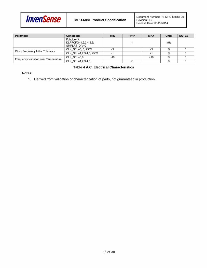
Parameter Conditions MIN TYP MAX Units NOTES
Fchoice=3; DLPFCFG=1,2,3,4,5,6; SMPLRT_DIV=0
1 kHz
Clock Frequency Initial Tolerance CLK_SEL=0, 6; 25°C -5 +5 % 1 CLK_SEL=1,2,3,4,5; 25°C -1 +1 % 1
Frequency Variation over Temperature CLK_SEL=0,6 -10 +10 % 1 CLK_SEL=1,2,3,4,5 ±1 % 1
Table 4 A.C. Electrical Characteristics
Notes:
1. Derived from validation or characterization of parts, not guaranteed in production.
MPU-6881 Product Specification Document Number: PS-MPU-6881A-00 Revision: 1.0 Release Date: 05/22/2014
14 of 38
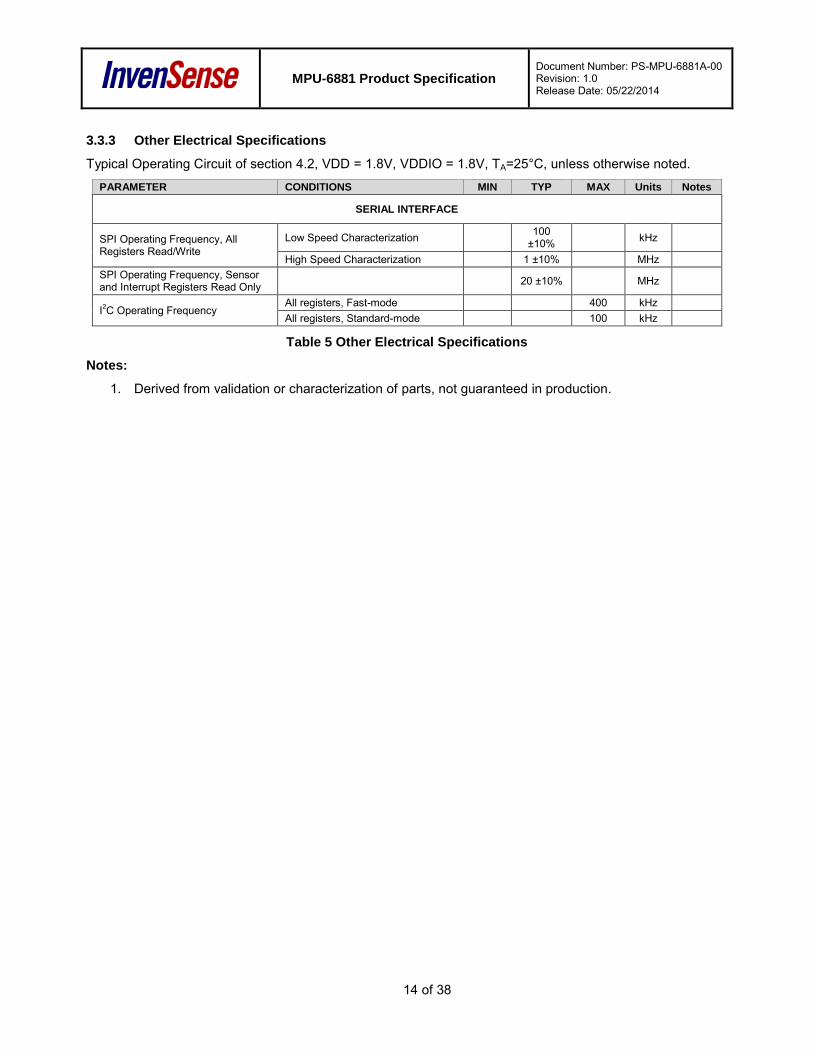
3.3.3 Other Electrical Specifications
Typical Operating Circuit of section 4.2, VDD = 1.8V, VDDIO = 1.8V, TA=25°C, unless otherwise noted.
PARAMETER CONDITIONS MIN TYP MAX Units Notes
SERIAL INTERFACE
SPI Operating Frequency, All Registers Read/Write
Low Speed Characterization 100 ±10% kHz
High Speed Characterization 1 ±10% MHz SPI Operating Frequency, Sensor and Interrupt Registers Read Only 20 ±10% MHz
I2C Operating Frequency All registers, Fast-mode 400 kHz All registers, Standard-mode 100 kHz
Table 5 Other Electrical Specifications
Notes:
1. Derived from validation or characterization of parts, not guaranteed in production.
MPU-6881 Product Specification Document Number: PS-MPU-6881A-00 Revision: 1.0 Release Date: 05/22/2014
15 of 38
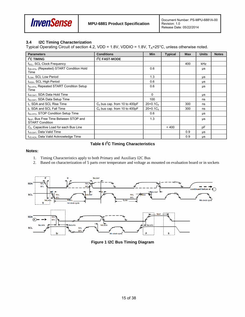
3.4 I2C Timing Characterization Typical Operating Circuit of section 4.2, VDD = 1.8V, VDDIO = 1.8V, TA=25°C, unless otherwise noted.
Parameters Conditions Min Typical Max Units Notes
I2C TIMING I
2C FAST-MODE
fSCL, SCL Clock Frequency 400 kHz tHD.STA, (Repeated) START Condition Hold Time
0.6 µs
tLOW, SCL Low Period 1.3 µs tHIGH, SCL High Period 0.6 µs tSU.STA, Repeated START Condition Setup Time
0.6 µs
tHD.DAT, SDA Data Hold Time 0 µs tSU.DAT, SDA Data Setup Time 100 ns tr, SDA and SCL Rise Time Cb bus cap. from 10 to 400pF 20+0.1Cb 300 ns tf, SDA and SCL Fall Time Cb bus cap. from 10 to 400pF 20+0.1Cb 300 ns tSU.STO, STOP Condition Setup Time 0.6 µs
tBUF, Bus Free Time Between STOP and START Condition
1.3 µs
Cb, Capacitive Load for each Bus Line < 400 pF tVD.DAT, Data Valid Time 0.9 µs tVD.ACK, Data Valid Acknowledge Time 0.9 µs
Table 6 I2C Timing Characteristics
Notes:
1. Timing Characteristics apply to both Primary and Auxiliary I2C Bus
2. Based on characterization of 5 parts over temperature and voltage as mounted on evaluation board or in sockets
Figure 1 I2C Bus Timing Diagram

MPU-6881 Product Specification Document Number: PS-MPU-6881A-00 Revision: 1.0 Release Date: 05/22/2014
16 of 38
3.5 SPI Timing Characterization
Typical Operating Circuit of section 4.2, VDD = 1.8V, VDDIO = 1.8V, TA=25°C, unless otherwise noted.
Parameters Conditions Min Typical Max Units Notes
SPI TIMING
fSCLK, SCLK Clock Frequency
1 MHz
tLOW, SCLK Low Period
400
ns
tHIGH, SCLK High Period
400
ns
tSU.CS, CS Setup Time
8
ns
tHD.CS, CS Hold Time
500
ns
tSU.SDI, SDI Setup Time
11
ns
tHD.SDI, SDI Hold Time
7
ns
tVD.SDO, SDO Valid Time Cload = 20pF
100 ns
tHD.SDO, SDO Hold Time Cload = 20pF 4
ns tDIS.SDO, SDO Output Disable Time
50 ns
Table 7 SPI Timing Characteristics
Notes:
3. Based on characterization of 5 parts over temperature and voltage as mounted on evaluation board or in sockets
Figure 2 SPI Bus Timing Diagram
3.5.1 fSCLK = 20MHz
Parameters Conditions Min Typical Max Units
SPI TIMING fSCLK, SCLK Clock Frequency 0.9 20 MHz
tLOW, SCLK Low Period - - ns
tHIGH, SCLK High Period - - ns
tSU.CS, CS Setup Time 1 ns
tHD.CS, CS Hold Time 1 ns

MPU-6881 Product Specification Document Number: PS-MPU-6881A-00 Revision: 1.0 Release Date: 05/22/2014
17 of 38
tSU.SDI, SDI Setup Time 0 ns
tHD.SDI, SDI Hold Time 1 ns
tVD.SDO, SDO Valid Time Cload = 20pF 25 ns
tDIS.SDO, SDO Output Disable Time 25 ns
Table 8 fCLK = 20MHz
Notes:
1. Based on characterization of 5 parts over temperature and voltage as mounted on evaluation board or in sockets
MPU-6881 Product Specification Document Number: PS-MPU-6881A-00 Revision: 1.0 Release Date: 05/22/2014
18 of 38
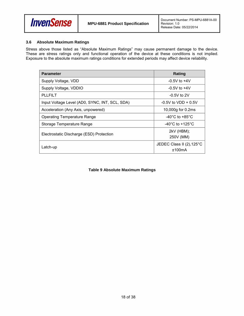
3.6 Absolute Maximum Ratings
Stress above those listed as “Absolute Maximum Ratings” may cause permanent damage to the device. These are stress ratings only and functional operation of the device at these conditions is not implied. Exposure to the absolute maximum ratings conditions for extended periods may affect device reliability.
Parameter Rating
Supply Voltage, VDD -0.5V to +4V
Supply Voltage, VDDIO -0.5V to +4V
PLLFILT -0.5V to 2V
Input Voltage Level (AD0, SYNC, INT, SCL, SDA) -0.5V to VDD + 0.5V
Acceleration (Any Axis, unpowered) 10,000g for 0.2ms
Operating Temperature Range -40°C to +85°C
Storage Temperature Range -40°C to +125°C
Electrostatic Discharge (ESD) Protection 2kV (HBM); 250V (MM)
Latch-up JEDEC Class II (2),125°C
±100mA
Table 9 Absolute Maximum Ratings

MPU-6881 Product Specification Document Number: PS-MPU-6881A-00 Revision: 1.0 Release Date: 05/22/2014
19 of 38
4 Applications Information
4.1 Pin Out Diagram and Signal Description
Pin Number Pin Name Pin Description
7 AUX_CL I2C Master serial clock, for connecting to external sensors 8 VDDIO Digital I/O supply voltage 9 AD0 / SDO I2C Slave Address LSB (AD0); SPI serial data output (SDO) 10 REGOUT Regulator filter capacitor connection 11 FSYNC Frame synchronization digital input. Connect to GND if unused. 12 INT Interrupt digital output (totem pole or open-drain) 13 VDD Power supply voltage and Digital I/O supply voltage 18 GND Power supply ground 19 RESV Reserved. Do not connect. 20 RESV Reserved. Connect to GND. 21 AUX_DA I2C master serial data, for connecting to external sensors 22 nCS Chip select (SPI mode only) 23 SCL / SCLK I2C serial clock (SCL); SPI serial clock (SCLK) 24 SDA / SDI I2C serial data (SDA); SPI serial data input (SDI)
1 – 6, 14 - 17 NC No Connect pins. Do not connect.
Table 10 Signal Descriptions
AU
X_C
L
VD
DIO
SD
O /
AD
0
RE
GO
UT
FSY
NC
INT
GND
SC
L / S
CLK
nCS
RE
SV
VDD
SD
A /
SD
I
NC
AU
X_D
A
RE
SV
NC
NC
NC
NC
NC
NC
NC
NC
NCMPU-6881
1
2
3
4
5
6 13
18
17
16
15
14
7 8 9 10 11 12
24 23 22 21 20 19
Figure 3 Pin out Diagram for MPU-6881 3.0x3.0x0.9mm QFN

MPU-6881 Product Specification Document Number: PS-MPU-6881A-00 Revision: 1.0 Release Date: 05/22/2014
20 of 38
4.2 Typical Operating Circuit
AUX_
CL
VDD
IO
SDO
/ AD
0
REG
OU
T
FSYN
C
INT
GND
SCL
/ SC
LK
nCS
RES
V
VDD
SDA
/ SD
I
NC
1.8 – 3.3VDC
C2, 0.1 mF
C3, 10 nF
1.8 – 3.3VDC
SCLVDDIO
SDA
AUX_
DA
AD0
C1, 0.1 mF
RES
V
NC
NC
NC
NC
NC
NC
NC
NC
NCMPU-6881
1
2
3
4
5
6 13
18
17
16
15
14
7 8 9 10 11 12
24 23 22 21 20 19
AUX_
CL
VDD
IO
SDO
/ AD
0
REG
OU
T
FSYN
C
INT
GND
SCL
/ SC
LK
nCS
RES
V
VDD
SDA
/ SD
I
NC
1.8 – 3.3VDC
C2, 0.1 mF
C3, 10 nF
1.8 – 3.3VDC
SCLKSDI
AUX_
DA
SD0
C1, 0.1 mF
RES
V
NC
NC
NC
NC
NC
NC
NC
NC
NCMPU-6881
1
2
3
4
5
6 13
18
17
16
15
14
7 8 9 10 11 12
24 23 22 21 20 19
nCS
(a) (b)
Figure 4 MPU-6881 QFN Application Schematic. (a) I2C operation, (b) SPI operation.
4.3 Bill of Materials for External Components
Component Label Specification Quantity
PLL Filter Capacitor C1 Ceramic, X7R, 0.1µF ±10%, 2V 1 VDD Bypass Capacitor C2 Ceramic, X7R, 0.1µF ±10%, 4V 1 VDDIO Bypass Capacitor C3 Ceramic, X7R, 10nF ±10%, 4V 1
Table 11 Bill of Materials

MPU-6881 Product Specification Document Number: PS-MPU-6881A-00 Revision: 1.0 Release Date: 05/22/2014
21 of 38
4.4 Block Diagram
MPU-6881
Charge
Pump
/CS
AD0 / SDO
SCL / SCLK
SDA / SDI
Temp Sensor ADC
ADCZ Gyro
ADCY Gyro
SYNC
Slave I2C and
SPI Serial
Interface
INTInterrupt
Status
Register
VDD
Bias & LDOs
GND PLLFILT
Z Accel
Y Accel
X Accel ADC
ADC
ADC
ADCX Gyro
Sig
na
l Co
nd
ition
ing
FIFO
User & Config
Registers
Sensor
Registers
Self
test
Self
test
Self
test
Self
test
Self
test
Self
test
Figure 5 MPU-6881 Block Diagram
4.5 Overview
The MPU-6881 is comprised of the following key blocks and functions:
Three-axis MEMS rate gyroscope sensor with 16-bit ADCs and signal conditioning Three-axis MEMS accelerometer sensor with 16-bit ADCs and signal conditioning Primary I2C and SPI serial communications interfaces Auxiliary I2C serial interface Self-Test Clocking Sensor Data Registers FIFO Interrupts Digital-Output Temperature Sensor Bias and LDOs Charge Pump Standard Power Modes

MPU-6881 Product Specification Document Number: PS-MPU-6881A-00 Revision: 1.0 Release Date: 05/22/2014
22 of 38
4.6 Three-Axis MEMS Gyroscope with 16-bit ADCs and Signal Conditioning
The MPU-6881 consists of three independent vibratory MEMS rate gyroscopes, which detect rotation about the X-, Y-, and Z- Axes. When the gyros are rotated about any of the sense axes, the Coriolis Effect causes a vibration that is detected by a capacitive pickoff. The resulting signal is amplified, demodulated, and filtered to produce a voltage that is proportional to the angular rate. This voltage is digitized using individual on-chip 16-bit Analog-to-Digital Converters (ADCs) to sample each axis. The full-scale range of the gyro sensors may be digitally programmed to ±250, ±500, ±1000, or ±2000 degrees per second (dps). The ADC sample rate is programmable from 8,000 samples per second, down to 3.9 samples per second, and user-selectable low-pass filters enable a wide range of cut-off frequencies.
4.7 Three-Axis MEMS Accelerometer with 16-bit ADCs and Signal Conditioning
The MPU-6881’s 3-Axis accelerometer uses separate proof masses for each axis. Acceleration along a particular axis induces displacement on the corresponding proof mass, and capacitive sensors detect the displacement differentially. The MPU-6881’s architecture reduces the accelerometers’ susceptibility to fabrication variations as well as to thermal drift. When the device is placed on a flat surface, it will measure 0g on the X- and Y-axes and +1g on the Z-axis. The accelerometers’ scale factor is calibrated at the factory and is nominally independent of supply voltage. Each sensor has a dedicated sigma-delta ADC for providing digital outputs. The full scale range of the digital output can be adjusted to ±2g, ±4g, ±8g, or ±16g.
4.8 I2C and SPI Serial Communications Interfaces
The MPU-6881 communicates to a system processor using either a SPI or an I2C serial interface. The MPU-6881 always acts as a slave when communicating to the system processor. The LSB of the of the I2C slave address is set by pin 4 (AD0).
4.8.1 MPU-6881 Solution Using I2C Interface
In the figure below, the system processor is an I2C master to the MPU-6881.

MPU-6881 Product Specification Document Number: PS-MPU-6881A-00 Revision: 1.0 Release Date: 05/22/2014
23 of 38
MPU-6881 AD0
SCL
SDA/SDI
Interrupt
Status
Register
INT
VDD
Bias & LDOs
GND PLLFILT
FIFO
User & Config
Registers
Sensor
Register
Factory
Calibration
Slave I2C
or SPI
Serial
Interface
System
Processor
SCL
SDA
VDD or GND
I2C Processor Bus: for reading all
sensor data from MPU
Figure 6 MPU-6881 Solution Using I2C Interface

MPU-6881 Product Specification Document Number: PS-MPU-6881A-00 Revision: 1.0 Release Date: 05/22/2014
24 of 38
4.8.2 MPU-6881 Solution Using SPI Interface
In the figure below, the system processor is an SPI master to the MPU-6881. Pins 2, 3, 4, and 5 are used to support the SCLK, SDI, SDO, and CS signals for SPI communications.
MPU-6881SDO
SCLK
SDI
Interrupt
Status
Register
INT
FIFO
Config
Register
Sensor
Register
Factory
Calibration
/CS
Slave I2C
or SPI
Serial
Interface
System
Processor
SDI
SCLK
SDO
nCS
Processor SPI Bus: for reading all
data from MPU and for configuring
MPU
VDD
Bias & LDOs
GND PLLFILT Figure 7 MPU-6881 Solution Using SPI Interface
4.9 Self-Test
Please refer to the register map document for more details on self-test.
Self-test allows for the testing of the mechanical and electrical portions of the sensors. The self-test for each measurement axis can be activated by means of the gyroscope and accelerometer self-test registers (registers 13 to 16).
When the self-test is activated, the electronics cause the sensors to be actuated and produce an output signal. The output signal is used to observe the self-test response.
The self-test response is defined as follows:
Self-test response = Sensor output with self-test enabled – Sensor output without self-test enabled
The self-test response for each gyroscope axis is defined in the gyroscope specification table, while that for each accelerometer axis is defined in the accelerometer specification table.
When the value of the self-test response is within the specified min/max limits of the product specification, the part has passed self-test. When the self-test response exceeds the min/max values, the part is deemed to have failed self-test. It is recommended to use InvenSense MotionApps software for executing self-test.

MPU-6881 Product Specification Document Number: PS-MPU-6881A-00 Revision: 1.0 Release Date: 05/22/2014
25 of 38
4.10 Clocking
The MPU-6881 has a flexible clocking scheme, allowing a variety of internal clock sources to be used for the internal synchronous circuitry. This synchronous circuitry includes the signal conditioning and ADCs, and various control circuits and registers. An on-chip PLL provides flexibility in the allowable inputs for generating this clock.
Allowable internal sources for generating the internal clock are:
An internal relaxation oscillator Any of the X, Y, or Z gyros (MEMS oscillators with a variation of ±1% over temperature)
Selection of the source for generating the internal synchronous clock depends on the requirements for power consumption and clock accuracy. These requirements will most likely vary by mode of operation.
There are also start-up conditions to consider. When the MPU-6881 first starts up, the device uses its internal clock until programmed to operate from another source. This allows the user, for example, to wait for the MEMS oscillators to stabilize before they are selected as the clock source.
4.11 Sensor Data Registers
The sensor data registers contain the latest gyro, accelerometer, auxiliary sensor, and temperature measurement data. They are read-only registers, and are accessed via the serial interface. Data from these registers may be read anytime.
4.12 FIFO
The MPU-6881 contains a 4096-byte FIFO register that is accessible via the Serial Interface. The FIFO configuration register determines which data is written into the FIFO. Possible choices include gyro data, accelerometer data, temperature readings, auxiliary sensor readings, and SYNC input. A FIFO counter keeps track of how many bytes of valid data are contained in the FIFO. The FIFO register supports burst reads. The interrupt function may be used to determine when new data is available.
For further information regarding the FIFO, please refer to the MPU-6881 Register Map and Register Descriptions document.
4.13 Interrupts
Interrupt functionality is configured via the Interrupt Configuration register. Items that are configurable include the INT pin configuration, the interrupt latching and clearing method, and triggers for the interrupt. Items that can trigger an interrupt are (1) Clock generator locked to new reference oscillator (used when switching clock sources); (2) new data is available to be read (from the FIFO and Data registers); (3) accelerometer event interrupts; and (4) the MPU-6881 did not receive an acknowledge from an auxiliary sensor on the secondary I2C bus. The interrupt status can be read from the Interrupt Status register.
For further information regarding interrupts, please refer to the MPU-6881 Register Map and Register Descriptions document.
4.14 Digital-Output Temperature Sensor
An on-chip temperature sensor and ADC are used to measure the MPU-6881 die temperature. The readings from the ADC can be read from the FIFO or the Sensor Data registers.
MPU-6881 Product Specification Document Number: PS-MPU-6881A-00 Revision: 1.0 Release Date: 05/22/2014
26 of 38
4.15 Bias and LDOs
The bias and LDO section generates the internal supply and the reference voltages and currents required by the MPU-6881. Its two inputs are an unregulated VDD and a VDDIO logic reference supply voltage. The LDO output is bypassed by a capacitor at PLLFILT. For further details on the capacitor, please refer to the Bill of Materials for External Components.
4.16 Charge Pump
An on-chip charge pump generates the high voltage required for the MEMS oscillators.
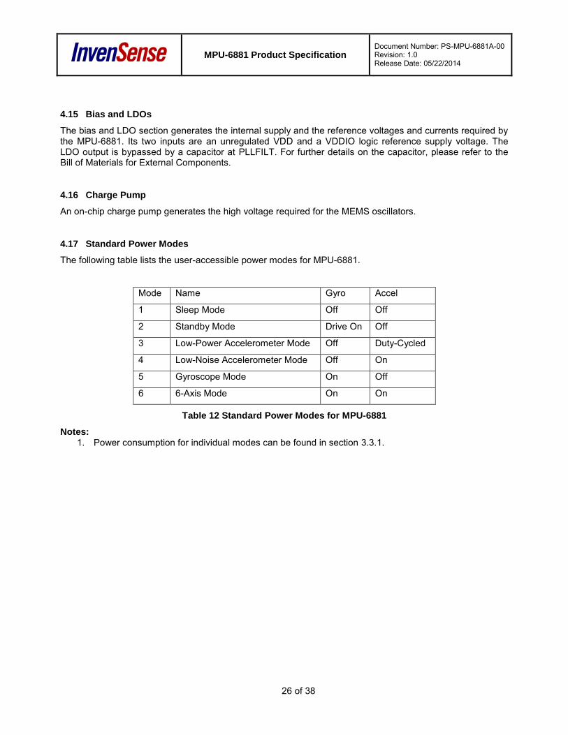
4.17 Standard Power Modes
The following table lists the user-accessible power modes for MPU-6881.
Mode Name Gyro Accel
1 Sleep Mode Off Off
2 Standby Mode Drive On Off
3 Low-Power Accelerometer Mode Off Duty-Cycled
4 Low-Noise Accelerometer Mode Off On
5 Gyroscope Mode On Off
6 6-Axis Mode On On
Table 12 Standard Power Modes for MPU-6881
Notes: 1. Power consumption for individual modes can be found in section 3.3.1.

MPU-6881 Product Specification Document Number: PS-MPU-6881A-00 Revision: 1.0 Release Date: 05/22/2014
27 of 38
5 Programmable Interrupts
The MPU-6881 has a programmable interrupt system which can generate an interrupt signal on the INT pin. Status flags indicate the source of an interrupt. Interrupt sources may be enabled and disabled individually.
Interrupt Name Module
FIFO Overflow FIFO
Data Ready Sensor Registers
I2C Master errors: Lost Arbitration, NACKs I2C Master
I2C Slave 4 I2C Master
Table 13 Table of Interrupt Sources
For information regarding the interrupt enable/disable registers and flag registers, please refer to the MPU-6881 Register Map and Register Descriptions document. Some interrupt sources are explained below.

MPU-6881 Product Specification Document Number: PS-MPU-6881A-00 Revision: 1.0 Release Date: 05/22/2014
28 of 38
6 Digital Interface
6.1 I2C and SPI Serial Interfaces
The internal registers and memory of the MPU-6881 can be accessed using either I2C at 400 kHz or SPI at 1MHz. SPI operates in four-wire mode.
Pin Number Pin Name Pin Description
8 VDDIO Digital I/O supply voltage.
9 AD0 / SDO I2C Slave Address LSB (AD0); SPI serial data output (SDO)
23 SCL / SCLK I2C serial clock (SCL); SPI serial clock (SCLK)
24 SDA / SDI I2C serial data (SDA); SPI serial data input (SDI)
Table 14 Serial Interface
Note:
To prevent switching into I2C mode when using SPI, the I2C interface should be disabled by setting the I2C_IF_DIS configuration bit. Setting this bit should be performed immediately after waiting for the time specified by the “Start-Up Time for Register Read/Write” in Section 6.3.
For further information regarding the I2C_IF_DIS bit, please refer to the MPU-6881 Register Map and Register Descriptions document.
6.2 I2C Interface
I2C is a two-wire interface comprised of the signals serial data (SDA) and serial clock (SCL). In general, the lines are open-drain and bi-directional. In a generalized I2C interface implementation, attached devices can be a master or a slave. The master device puts the slave address on the bus, and the slave device with the matching address acknowledges the master.
The MPU-6881 always operates as a slave device when communicating to the system processor, which thus acts as the master. SDA and SCL lines typically need pull-up resistors to VDD. The maximum bus speed is 400 kHz.
The slave address of the MPU-6881 is b110100X which is 7 bits long. The LSB bit of the 7 bit address is determined by the logic level on pin AD0. This allows two MPU-6881s to be connected to the same I2C bus. When used in this configuration, the address of the one of the devices should be b1101000 (pin AD0 is logic low) and the address of the other should be b1101001 (pin AD0 is logic high).
6.3 I2C Communications Protocol
START (S) and STOP (P) Conditions
Communication on the I2C bus starts when the master puts the START condition (S) on the bus, which is defined as a HIGH-to-LOW transition of the SDA line while SCL line is HIGH (see figure below). The bus is considered to be busy until the master puts a STOP condition (P) on the bus, which is defined as a LOW to HIGH transition on the SDA line while SCL is HIGH (see figure below).
Additionally, the bus remains busy if a repeated START (Sr) is generated instead of a STOP condition.
MPU-6881 Product Specification Document Number: PS-MPU-6881A-00 Revision: 1.0 Release Date: 05/22/2014
29 of 38
SDA
SCLS
START condition STOP condition
P
Figure 8 START and STOP Conditions
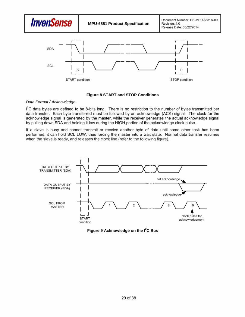
Data Format / Acknowledge
I2C data bytes are defined to be 8-bits long. There is no restriction to the number of bytes transmitted per data transfer. Each byte transferred must be followed by an acknowledge (ACK) signal. The clock for the acknowledge signal is generated by the master, while the receiver generates the actual acknowledge signal by pulling down SDA and holding it low during the HIGH portion of the acknowledge clock pulse.
If a slave is busy and cannot transmit or receive another byte of data until some other task has been performed, it can hold SCL LOW, thus forcing the master into a wait state. Normal data transfer resumes when the slave is ready, and releases the clock line (refer to the following figure).
DATA OUTPUT BY TRANSMITTER (SDA)
DATA OUTPUT BY RECEIVER (SDA)
SCL FROM MASTER
START condition
clock pulse for acknowledgement
acknowledge
not acknowledge
1 2 8 9
Figure 9 Acknowledge on the I
2C Bus

MPU-6881 Product Specification Document Number: PS-MPU-6881A-00 Revision: 1.0 Release Date: 05/22/2014
30 of 38
Communications
After beginning communications with the START condition (S), the master sends a 7-bit slave address followed by an 8th bit, the read/write bit. The read/write bit indicates whether the master is receiving data from or is writing to the slave device. Then, the master releases the SDA line and waits for the acknowledge signal (ACK) from the slave device. Each byte transferred must be followed by an acknowledge bit. To acknowledge, the slave device pulls the SDA line LOW and keeps it LOW for the high period of the SCL line. Data transmission is always terminated by the master with a STOP condition (P), thus freeing the communications line. However, the master can generate a repeated START condition (Sr), and address another slave without first generating a STOP condition (P). A LOW to HIGH transition on the SDA line while SCL is HIGH defines the stop condition. All SDA changes should take place when SCL is low, with the exception of start and stop conditions.
SDA
START condition
SCL
ADDRESS R/W ACK DATA ACK DATA ACK STOP condition
S P
1 – 7 8 9 1 – 7 8 9 1 – 7 8 9
Figure 10 Complete I2C Data Transfer
To write the internal MPU-6881 registers, the master transmits the start condition (S), followed by the I2C address and the write bit (0). At the 9th clock cycle (when the clock is high), the MPU-6881 acknowledges the transfer. Then the master puts the register address (RA) on the bus. After the MPU-6881 acknowledges the reception of the register address, the master puts the register data onto the bus. This is followed by the ACK signal, and data transfer may be concluded by the stop condition (P). To write multiple bytes after the last ACK signal, the master can continue outputting data rather than transmitting a stop signal. In this case, the MPU-6881 automatically increments the register address and loads the data to the appropriate register. The following figures show single and two-byte write sequences.
Single-Byte Write Sequence
Burst Write Sequence
Master S AD+W RA DATA P
Slave ACK ACK ACK
Master S AD+W RA DATA DATA P
Slave ACK ACK ACK ACK

MPU-6881 Product Specification Document Number: PS-MPU-6881A-00 Revision: 1.0 Release Date: 05/22/2014
31 of 38
To read the internal MPU-6881 registers, the master sends a start condition, followed by the I2C address and a write bit, and then the register address that is going to be read. Upon receiving the ACK signal from the MPU-6881, the master transmits a start signal followed by the slave address and read bit. As a result, the MPU-6881 sends an ACK signal and the data. The communication ends with a not acknowledge (NACK) signal and a stop bit from master. The NACK condition is defined such that the SDA line remains high at the 9th clock cycle. The following figures show single and two-byte read sequences.
Single-Byte Read Sequence
Burst Read Sequence
6.4 I2C Terms
Signal Description
S Start Condition: SDA goes from high to low while SCL is high AD Slave I2C address W Write bit (0) R Read bit (1)
ACK Acknowledge: SDA line is low while the SCL line is high at the 9th clock cycle
NACK Not-Acknowledge: SDA line stays high at the 9th clock cycle RA MPU-6881 internal register address
DATA Transmit or received data P Stop condition: SDA going from low to high while SCL is high
Table 15 I2C Terms
Master S AD+W RA S AD+R NACK P
Slave ACK ACK ACK DATA
Master S AD+W RA S AD+R ACK NACK P
Slave ACK ACK ACK DATA DATA

MPU-6881 Product Specification Document Number: PS-MPU-6881A-00 Revision: 1.0 Release Date: 05/22/2014
32 of 38
6.5 SPI Interface
SPI is a 4-wire synchronous serial interface that uses two control lines and two data lines. The MPU-6881 always operates as a Slave device during standard Master-Slave SPI operation.
With respect to the Master, the Serial Clock output (SCLK), the Serial Data Output (SDO) and the Serial Data Input (SDI) are shared among the Slave devices. Each SPI slave device requires its own Chip Select (CS) line from the master.
CS goes low (active) at the start of transmission and goes back high (inactive) at the end. Only one CS line is active at a time, ensuring that only one slave is selected at any given time. The CS lines of the non-selected slave devices are held high, causing their SDO lines to remain in a high-impedance (high-z) state so that they do not interfere with any active devices.
SPI Operational Features
1. Data is delivered MSB first and LSB last 2. Data is latched on the rising edge of SCLK 3. Data should be transitioned on the falling edge of SCLK 4. The maximum frequency of SCLK is 1MHz 5. SPI read and write operations are completed in 16 or more clock cycles (two or more bytes). The
first byte contains the SPI Address, and the following byte(s) contain(s) the SPI data. The first bit of the first byte contains the Read/Write bit and indicates the Read (1) or Write (0) operation. The following 7 bits contain the Register Address. In cases of multiple-byte Read/Writes, data is two or more bytes:
SPI Address format
MSB LSB
R/W A6 A5 A4 A3 A2 A1 A0
SPI Data format
MSB LSB
D7 D6 D5 D4 D3 D2 D1 D0
6. Supports Single or Burst Read/Writes.
SPI Master SPI Slave 1
SPI Slave 2
/CS1 /CS2
SCLKSDI
SDO/CS
SCLKSDI
SDO/CS
Figure 11 Typical SPI Master / Slave Configuration

MPU-6881 Product Specification Document Number: PS-MPU-6881A-00 Revision: 1.0 Release Date: 05/22/2014
33 of 38
7 Serial Interface Considerations
7.1 MPU-6881 Supported Interfaces
The MPU-6881 supports I2C communications on its serial interface.
The MPU-6881’s I/O logic levels are set to be VDDIO.
The figure below depicts a sample circuit of MPU-6881. It shows the relevant logic levels and voltage connections.
MPU-6881
VDD
System Processor IO
SYSTEM BUS
VDDIO
VDDIO
VDD
VDDIO
SCL
SDA
INT
FSYNC
VDDIO
AD0
(0V - VDDIO)
(0V - VDDIO)(0V - VDDIO)
(0V - VDDIO)
(0V - VDDIO)
(0V, VDDIO)
VDD_IO
Figure 12 I/O Levels and Connections
MPU-6881 Product Specification Document Number: PS-MPU-6881A-00 Revision: 1.0 Release Date: 05/22/2014
34 of 38
8 Assembly
This section provides general guidelines for assembling InvenSense Micro Electro-Mechanical Systems (MEMS) gyros packaged in QFN package.
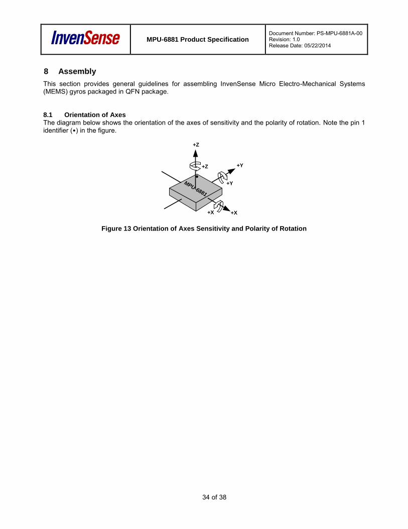
8.1 Orientation of Axes The diagram below shows the orientation of the axes of sensitivity and the polarity of rotation. Note the pin 1 identifier (•) in the figure.
MPU-6881
+Z
+X
+Y
+Z
+Y
+X
Figure 13 Orientation of Axes Sensitivity and Polarity of Rotation

MPU-6881 Product Specification Document Number: PS-MPU-6881A-00 Revision: 1.0 Release Date: 05/22/2014
35 of 38
8.2 Package Dimensions
24 Lead QFN (3x3x0.9) mm NiPdAu Lead-frame finish
DIMENSIONS IN MILLIMETERS
SYMBOLS DESCRIPTION MIN NOM MAX
A Package thickness 0.85 0.90 0.95 A1 Lead finger (pad) seating height 0.00 0.02 0.05 b Lead finger (pad) width 0.15 0.20 0.25 c Lead frame (pad) height --- 0.20 REF --- D Package width 2.90 3.00 3.10
D2 Exposed pad width 1.65 1.70 1.75 E Package length 2.90 3.00 3.10
E2 Exposed pad length 1.49 1.54 1.59 e Lead finger-finger (pad-pad) pitch --- 0.40 ---
f (e-b) Lead-lead (Pad-Pad) space 0.15 0.20 0.25 K Lead (pad) to Exposed Pad Space --- 0.35 REF --- L Lead (pad) length 0.25 0.30 0.35 R Lead (pad) corner radius 0.075 REF --- R’ Corner lead (pad) outer radius 0.10 0.11 0.12 R’’ Corner lead (pad) inner radius 0.10 0.11 0.12 s Corner lead-lead (pad-pad) spacing --- 0.25 REF --- h Corner lead dimension 0.22 w Corner lead dimension 0.12 y Lead Conformality 0.00 --- 0.075
h
w

MPU-6881 Product Specification Document Number: PS-MPU-6881A-00 Revision: 1.0 Release Date: 05/22/2014
36 of 38
9 Part Number Package Marking
The part number package marking for MPU-6881 devices is summarized below:
Part Number Part Number Package Marking
MPU-6881 MP688

MPU-6881 Product Specification Document Number: PS-MPU-6881A-00 Revision: 1.0 Release Date: 05/22/2014
37 of 38
10 Reliability
10.1 Qualification Test Policy
InvenSense’s products complete a Qualification Test Plan before being released to production. The Qualification Test Plan for the MPU-6881 followed the JESD47I Standards, “Stress-Test-Driven Qualification of Integrated Circuits,” with the individual tests described below.
10.2 Qualification Test Plan
Accelerated Life Tests
TEST Method/Condition
Lot Quantity
Sample / Lot
Acc / Reject Criteria
(HTOL/LFR) High Temperature Operating Life
JEDEC JESD22-A108D, Dynamic, 3.63V biased, Tj>125°C [read-points 168, 500, 1000 hours]
3 77 (0/1)
(HAST) Highly Accelerated Stress Test (1)
JEDEC JESD22-A118A Condition A, 130°C, 85%RH, 33.3 psia., unbiased, [read-point 96 hours]
3 77 (0/1)
(HTS) High Temperature Storage Life
JEDEC JESD22-A103D, Cond. A, 125°C Non-Bias Bake [read-points 168, 500, 1000 hours]
3
77 (0/1)
Device Component Level Tests
TEST Method/Condition
Lot Quantity
Sample / Lot
Acc / Reject Criteria
(ESD-HBM) ESD-Human Body Model
JEDEC JS-001-2012, (2.0 KV) 1 3 (0/1)
(ESD-MM) ESD-Machine Model
JEDEC JESD22-A115C, (250V) 1 3 (0/1)
(LU) Latch Up
JEDEC JESD-78D Class II (2), 125°C; ±100mA 1 6 (0/1)
(MS) Mechanical Shock
JEDEC JESD22-B104C, Mil-Std-883, Method 2002.5, Cond. E, 10,000g’s, 0.2ms, ±X, Y, Z – 6 directions, 5 times/direction
3
5
(0/1)
(VIB) Vibration
JEDEC JESD22-B103B, Variable Frequency (random), Cond. B, 5-500Hz, X, Y, Z – 4 times/direction
3 5 (0/1)
Temperature Cycling (TC) (1) JEDEC JESD22-A104D Condition G, [-40°C to +125°C], Soak Mode 2 [5’], 850 cycles
3 77 (0/1)
(1) Tests are preceded by MSL3 Preconditioning in accordance with JEDEC JESD22-A113F
MPU-6881 Product Specification Document Number: PS-MPU-6881A-00 Revision: 1.0 Release Date: 05/22/2014
38 of 38
11 Reference Please refer to “InvenSense MEMS Handling Application Note (AN-IVS-0002A-00)” for the following information:
Manufacturing Recommendations o Assembly Guidelines and Recommendations o PCB Design Guidelines and Recommendations o MEMS Handling Instructions o ESD Considerations o Reflow Specification o Storage Specifications o Package Marking Specification o Tape & Reel Specification o Reel & Pizza Box Label o Packaging o Representative Shipping Carton Label
Compliance o Environmental Compliance o DRC Compliance o Compliance Declaration Disclaimer
This information furnished by InvenSense is believed to be accurate and reliable. However, no responsibility is assumed by InvenSense for its use, or for any infringements of patents or other rights of third parties that may result from its use. Specifications are subject to change without notice. InvenSense reserves the right to make changes to this product, including its circuits and software, in order to improve its design and/or performance, without prior notice. InvenSense makes no warranties, neither expressed nor implied, regarding the information and specifications contained in this document. InvenSense assumes no responsibility for any claims or damages arising from information contained in this document, or from the use of products and services detailed therein. This includes, but is not limited to, claims or damages based on the infringement of patents, copyrights, mask work and/or other intellectual property rights.
Certain intellectual property owned by InvenSense and described in this document is patent protected. No license is granted by implication or otherwise under any patent or patent rights of InvenSense. This publication supersedes and replaces all information previously supplied. Trademarks that are registered trademarks are the property of their respective companies. InvenSense sensors should not be used or sold in the development, storage, production or utilization of any conventional or mass-destructive weapons or for any other weapons or life threatening applications, as well as in any other life critical applications such as medical equipment, transportation, aerospace and nuclear instruments, undersea equipment, power plant equipment, disaster prevention and crime prevention equipment.
©2014 InvenSense, Inc. All rights reserved. InvenSense, MotionTracking, MotionProcessing, MotionProcessor, MotionFusion, MotionApps, DMP, AAR, and the InvenSense logo are trademarks of InvenSense, Inc. Other company and product names may be trademarks of the respective companies with which they are associated.
©2014 InvenSense, Inc. All rights reserved.