Embed Size (px)
Citation preview

Revision History Rev. Date Author Description 1.0 28/9/12 Paolo Musico First revision, integrates “MPD FPGA
Specifications” v.3.0 2.0 3/6/14 Paolo Musico Include MPD 4.0 and new VME interface and
memory map 2.1 10/11/15 Paolo Musico Added Optical Fiber inteface

www.ge.infn.it/~musico Rev 2.1 ii
Contents MPD Specifications i Introduction 1 Main Features 2
Clocking 4 Front Panel 4 J33, … , J40: LEMO I/O level selectors for rev 3.0 only 6
VME Usage 7 Geographical addressing and A24 Base Address 7 A24 Space 8
ADS5281 (ADCs) configuration registers 12 I2C Controller Registers 13 Histogrammer registers and memory 14 APV Acquisition control registers and FIFOs 15 Pedestals and Thresholds RAMs 17 Trigger Time FIFO 18 SDRAM Chip Direct Access 19 SDRAM output FIFO 19
Fiber interface 20 FIR filters 21 Implementation 22
FPGA BLOCK DIAGRAM 22 TRIGGER GENERATOR MODULE 22 CHANNEL PROCESSOR MODULE 23 EVENT BUILDER MODULE 25 SDRAM FIFO INTERFACE MODULE 27
References 28

Introduction The MPD (Multi Purpose Digitizer) Board has been designed to completely handle up to 16 APV front-end cards, reading out the corresponding analog data streams and transmitting both the control and configuration signals. After the A/D conversion the input signals can be conditioned by means of 16-tap FIR filters (one each channel). Thanks to the use of a large FPGA and abundant on board resources, its use is not limited only to handle the APV25 in the Jlab SBS scenario, but can be arranged also for other purposes. Here we specify the functionalities of the board in release 3.0 and 4.0. Release 4.0 has been developed to avoid the use of expensive and not easily procurable HDMI-B cables, initially adopted for the differential input analog signals. The board has been implemented in VME 6U x 160 mm format, as seen in fig. 1.
Fig. 1 MPD rev 3.0 on the left, MPD rev 4.0 on the right

www.ge.infn.it/~musico Rev 2.0 2 of 28
Main Features The two versions of MPDs block diagram are represented in fig 2 and fig. 3.
Fig. 2 The MPD rev 3.0 block diagram
Fig. 3 The MPD rev 4.0 block diagram

www.ge.infn.it/~musico Rev 2.0 3 of 28
The core of the board is an Altera ARRIA GX FPGA: EP1AGX50DF780C6N in rev 3.0 and a larger EP1AGX60DF780C6N in rev 4.0. The FPGA will handle: VME interface (VME64x with VXS extension and Jlab custom multiblock
transfer). ADS5281 interfacing (2 x 8 channels, up to 50 MHz (40 MHz typical), 12 bit
ADC, differential inputs, 2 Vpp, with DDR serial interface @ 480 Mbit/s). I2C protocol for on-board devices and APV25 configuration. APV25 triggering. Coaxial front panel I/O with configurable levels (LVTTL – NIM). Large memory buffer implemented with external DDR SDram (2 x Micron
MT46V64M8: 128 M x 8 bits in rev 3.0 and 1 x Micron MT47H128M8 in rev 4.0)
Large Flash memory buffer implemented with an external device in rev 3.0, replaced by a micro SD-Card interface in v 4.0
Ethernet 10-100 PHY. High speed optical protocol using SFP transceiver. Low speed USB interfacein rev 3.0, dropped in rev 4.0. Remote reconfiguration (firmware TBD). User configuration switches, LEDs, ... Expansion PMC connectors in rev 4.0. Rev 4.0 board introduces also some enhancements to improve S/N ratio on the converted data. Since some rev 3.0 boards are around, FPGA firmware will be maintained for both HW releases, giving to the user the same programmer model. Since all the required power supply voltages are generated on board starting from a single +5 V, the use of a VME crate is not mandatory. A user can also implement a table top or “satellite” system using Ethernet and/or optical transmission channels, collecting the data through standard network components. In this case (not developed yet) a System On a Chip (SOC) must be implemented, including soft-core microprocessor and high level Operating System (OS) to handle all the data transactions on the network by embedded custom software. The board is designed to fit in a VME-64x VXS crate. For large availabiliy of standard VME-32 and 64x systems the board will be provided with the VXS connector not mounted. So the board will fit in a VME-64x crate without any problem. If the user want to use a standard VME-32 crate the front panel has to be removed, since the guide pins will not fit. Custom VME32 front panel design could be an option. In case of using VME32 crate some care have to be paid manually assigning the board base address (see later). The ADC clock phase can be adjusted to compensate cable delays, using DELAY25 component available from CERN. In any case the delay chip must be configured.
www.ge.infn.it/~musico Rev 2.0 4 of 28
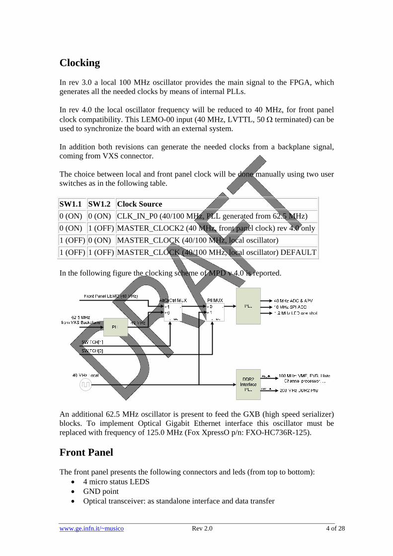
Clocking In rev 3.0 a local 100 MHz oscillator provides the main signal to the FPGA, which generates all the needed clocks by means of internal PLLs. In rev 4.0 the local oscillator frequency will be reduced to 40 MHz, for front panel clock compatibility. This LEMO-00 input (40 MHz, LVTTL, 50 terminated) can be used to synchronize the board with an external system. In addition both revisions can generate the needed clocks from a backplane signal, coming from VXS connector. The choice between local and front panel clock will be done manually using two user switches as in the following table.
SW1.1 SW1.2 Clock Source
0 (ON) 0 (ON) CLK_IN_P0 (40/100 MHz, PLL generated from 62.5 MHz)
0 (ON) 1 (OFF) MASTER_CLOCK2 (40 MHz, front panel clock) rev 4.0 only
1 (OFF) 0 (ON) MASTER_CLOCK (40/100 MHz, local oscillator)
1 (OFF) 1 (OFF) MASTER_CLOCK (40/100 MHz, local oscillator) DEFAULT
In the following figure the clocking scheme of MPD v 4.0 is reported.
An additional 62.5 MHz oscillator is present to feed the GXB (high speed serializer) blocks. To implement Optical Gigabit Ethernet interface this oscillator must be replaced with frequency of 125.0 MHz (Fox XpressO p/n: FXO-HC736R-125).
Front Panel The front panel presents the following connectors and leds (from top to bottom):
4 micro status LEDS GND point Optical transceiver: as standalone interface and data transfer

www.ge.infn.it/~musico Rev 2.0 5 of 28
Mini USB (in rev 3.0): as standalone interface 10/100 Ethernet RJ45: as standalone interface 2 Input LEMO connectors (4 in rev 3.0): user defined (trigger, clock …) 2 Output LEMO connectors (4 in rev 3.0): user defined (clock, busy …) 1 clock input: 40 MHz, LVTTL, 50 terminated, in rev 4.0 2 x HDMI-A: digital outputs (trigger, clock and I2C) to the APV cards 4 x HDMI-A (2 x HDMI-B in rev 3.0): analog inputs from APV cards
The 4 leds are available on the upper part of the MPD front panels. The LEDS blink according to the following table. Left LED Left-Mid LED Right-Mid LED Right LED Data access (VME/optical) Trigger to APVs I2C access Optical link UP Logic levels of the LEMO I/O connectors can be configured as NIM or TTL. In rev 4.0 selection is done via software registers of the FPGA; in rev 3.0 selection depend on jumpers J33 … J40. The upper left Input LEMO connector is by default the input of the TRIGGER signal. The second Input LEMO connector is by default the input of the SYNC signal. The upper left Output LEMO connector provides by default the BUSY signal. The second Output LEMO connector provides by default a 40 MHz clock. The 2 upper most HDMI-A connectors are used to output the APV digital signals (clock, trigger and I2C); they are generally connected to a backplane (or patch panel) that distribute the signals to the APV cards. The lower analog HDMI connectors receive the analog APV signals (4 signals, or channels for each HDMI-A, 8 for each HDMI-B). In rev 4.0 a special configuration permit to group up to 5 channels on two of the 4 input HDMI-A connectors; this is selected by solder jumpers on the MPD. On the printed board side, are hosted:
J9: JTAG connector for FPGA programming J10: FPGA Flash Prom programming connector (not used) J28: +5 V power connector, for stand alone operations J43: I2C Debug: SCL, SDA, GND J45, J46, J47, J48: GND connection for testing probes J33, … , J40: LEMO I/O level selectors (rev 3.0 only) J1005: front panel FASTON connected to GND J1009: Geographical address upper bit selection (for VME32 crate) SW1: USER Selection switches SW2: FPGA code selector (TBD) SW3: Geographic address selector (for VME32 crates) together with the J1009
jumper J1006-J1010: HDMI-A digital signals output connectors J1007-J1008: HDMI-B analog signals input connectors (rev 3.0 only) J2000-J2001, J2004-J2005: HDMI-A analog signals input connectors (rev 4.0
only)

www.ge.infn.it/~musico Rev 2.0 6 of 28
J2002-J2003, J2006-J2007: connect the 5th backplane channel to ADC for J2000 and J2004 respectively, as alternaltive to J2009-J2010, J2011-J2012. In this case the 1st channel on J2001 and J2005 is not connected
J2009-J2010, J2011-J2012: used to readout 4 channel HDMI-A as alternaltive to J2002-J2003, J2006-J2007
Piggyback connectors: PN1-J1, PN3-J3 electrically compatible with PMC standard (rev 4.0 only)
J33, … , J40: LEMO I/O level selectors for rev 3.0 only
Left picture shows LVTTL IO settings, while right picture shows NIM settings. Refer to the following table for details. JUMPER Related IO J37 Input 0 J40 Input 2 J38 Input 1 J39 Input 3 J33 Output 0 J36 Output 2 J34 Output 1 J35 Output 3

www.ge.infn.it/~musico Rev 2.0 7 of 28
VME Usage
The VME bus is the primary interface adopted by JLab DAQ environment and for this reason it was the first to be implemented and extensively tested. The protocol is handled using a custom developed block which implements the following cycles: Single A24 cycles: non privileged and supervisor program and data space,
CR/CSR space. They are all used to access configuration ROM, configuration registers and access to debug structures.
Single A32 cycles: non privileged and supervisor program and data space Block transfer A24 and A32 cycles: non privileged and supervisor MBLT A32 D64 cycles 2eVME cycles: A32 D64, master/slave terminated 2eSST cycles: A32 D64, master/slave terminated Jlab custom multiboard transfer (TBD)
The VME interface decodes various spaces:
A24: 256 kB for configuration registers, status registers, parameter and histogrammer RAMs, debug readout
A32: output buffer, SDRAM direct access (for debug), test module (for debug) A24 base address upper bits are stored in the BaseAddressRegister, which defaults to Geographical Address. A32 base addresses are stored into configuration registers.
Geographical addressing and A24 Base Address Using a Vme64x crate the GA lines are connected to the corresponding lines on the backplane. In a VME32 crate the GA lines must be set using a rotary switch (SW3) for GA[3:0] and a solder jumper (J1009) for GA[4]. Using a VME-64x crate SW3 must be placed in position 0 and J1009 must be left open. To ensure this compatibility the GAP (Geographical Address Parity) line is never checked. A24 Base Address register (mapped at A24BaseAddress+0x180) default value (at powerup or after a reset) is:
7..3 2..0
GA[4:0] 0 A24_BAR

www.ge.infn.it/~musico Rev 2.0 8 of 28
A24 Base Address is made up as follows:
23..18 17..0
A42_BAR[7:2] 0 A24BaseAddress
The following table summarizes the corrispondence between the VME64 Geographical address (slot position) or VME32 MPD rotary switch and the A24 default base address. GEO address (slot number) or rotary switch (VME32)
A24 base address (with A24_BAR = default)
1 0x080000 2 0x100000 3 0x180000 4 0x200000 5 0x280000 … … 19 0x980000 20 0xA00000
A24 Space In the A24 address space as previously defined, the following devices will be decoded, adding the Offset field to A24BaseAddress: Offset Length
(lwords) Description Value - Notes
0x00000 1 MAGIC VALUE 0x43524F4D = ‘CROM’ – RO
0x00004 1 MANUF_ID 0x00080030 – ReadOnly 0x00008 1 BOARD_ID 0x00030904 – ReadOnly 0x0000C 1 REVISION_ID 0x04000004 – ReadOnly 0x00010 1 COMPILE_TIME time_t – ReadOnly 0x00100 1 RESET_REG Not Used 0x00104 1 IO_CONFIG 0x00108 1 SAMPLE_PER_EVENT 0x0010C 1 EVENT_PER_BLOCK 0x00110 1 BUSY_THR 0x00114 1 BUSY_THR_LOCAL > BUSY_THR 0x00118 1 READOUT_CONFIG 0x0011C 1 TRIGGER_CONFIG 0x00120 1 TRIGGER_DELAY 0x00124 1 SYNC_PERIOD 0x00128 1 MARKER_CHANNEL 0x0012C 1 CHANNEL_ENABLE

www.ge.infn.it/~musico Rev 2.0 9 of 28
0x00130 1 ZERO_THRESHOLD 0x00134 1 ONE_THRESHOLD 0x00138 8 FIR_COEFFICIENTS 0x00180 1 A24_BAR 0x00184 1 MULTIBOARD_CONFIG TBD 0x00188 1 MULTIBOARD_ADD_LOW TBD 0x0018C 1 MULTIBOARD_ADD_HIGH TBD 0x00190 1 FIBER_STATUS_CTRL 0x00194 1 OBUF_BASE_ADDR 8 MBytes 0x00198 1 SDRAM_BASE_ADDR 8 MBytes 0x0019C 1 SDRAM_BANK 16 banks x 8 MB = 128 MB 0x00200 10 (up to 64) OUTPUT_BUFFER_STATUS 0x00300 1 ADC_CONFIG 0x00380 4 SERIAL MEMORY IF TBD 0x00390 4 REMOTE UPDATE TBD 0x00400 8 I2C_CONFIG 0x01000 2 HISTO0_REGISTERS StatusCtrl & Counter 0x01008 2 HISTO1_REGISTERS StatusCtrl & Counter 0x04000 4K HISTO0_RAM 0x08000 4K HISTO1_RAM 0x10000 16 × 1K CHANNELS_SPACE 0x30000 18 CHANNELS_FLAGS FIFO word count & flags 0x34000 16 × 128 PEDESTAL_RAM 0x36000 16 × 128 THRESHOLD_RAM Location 0x00000 – 0x00010 are read only identification parameters and can be used to identify the board. REVISION_ID holds HW revision ID (3 or 4) in the upper 8 bit and FPGA revision ID (4 or higher) in the lower 16 bit. COMPILE_TIME contains the FPGA compile time in time_t format. Location 0x00100 – 0x0019C are configuration registers. All locations in the table above can be accessed with both VME and Fiber interface, except the locations from 0x00180 to 0x0019C accessed only through the VME. Location 0x0200 – 0x02FC Output Buffer status registers: 0x0200 EVB_FIFO_WORD_COUNT: Words present in the Event Builder
output FIFO and related flags {4'h0,OUT_FIFO_FULL_L,EVB_FIFO_FULL_L,EVTCNT_FIFO_FULL_L, TIME_FIFO_FULL_L, 6'h0, FULL, EMPTY, 4'h0, WORD_COUNT[11:0]}
0x0204 EVENT_COUNT: Event counted by Event Builder (24 bit) 0x0208 BLOCK_COUNT: Block counted by Event Builder (8 bit) 0x020C TRIGGER_COUNT: Number of trigger sent to APVs

www.ge.infn.it/~musico Rev 2.0 10 of 28
0x0210 MISSED_TRIGGER: Number of trigger received but not sent to APVs, due to input FIFO congestion
0x0214 INCOMING_TRIGGER: Number of trigger received 0x0218 SDRAM_FIFO_WR_ADDR: {SDR_OK, 6’h0, WR_ADDR[24:0]} 0x021C SDRAM_FIFO_RD_ADDR: {SDR_OK, 6’h0, RD_ADDR[24:0]} 0x0220 SDRAM_FLAG_WC: {OVERRUN, 6’h0, WORD_COUNT[24:0]} 0x0224 OBUF_STATUS: {FULL, EMPTY, 17’h0, WORD_COUNT[12:0]} 0x0228 Latched_Full: {APV_FIFO_FULL_L, PROCESS_FIFO_FULL_L}
SDRAM* registers are intended to be used for debug. SDR_OK = 1 means that the SDRAM is working properly. If OVERRUN = 1 everything must be restarted. xxx_FULL_L are the FIFO full flags latched: if ‘1’ at least one time the corresponding fifo went full. They will be cleared only with a restart of the DAQ.
MULTIBOARD CONFIGURATION: To Be Defined. FIBER STATUS & CONTROL:
[0] = Fiber Disable (1 = disabled) [1] = SFP transmit disable (1 = disabled) [2] = Spare [3] = Fiber Reset (1 = reset) [11:4] = Fiber Error Count (Read Only) [12] = Fiber Frame Error (Read Only) [13] = Fiber Hard Error (Read Only) [14] = SFP Present – active low (Read Only) [15] = SFP Loss of Signal (Read Only) [30:16] = Spare [31] = Fiber Channel UP (Read Only)
Note that after power up or reset, the fiber interface is enabled by default: to access board resources with VME it must be disabled setting to 1 bit 0 (and also bit 1) of FIBER_STATUS_CTRLregister. OUTPUT BUFFER BASE ADDRESS: Address for A32 accesses of the Output FIFO Data Buffer. Address space is 8 Mbytes. The value written here must be the effective base address shifted right by 2 positions. SDRAM BASE ADDRESS: Address for A32 accesses of the DDR2 SDRAM. Address space is 8 Mbytes. Used for debug only. The value written here must be the effective base address shifted right by 2 positions. SDRAM BANK: Bank index (from 0 to 15) for A32 accesses of the DDR2 SDRAM. Used for debug only.

www.ge.infn.it/~musico Rev 2.0 11 of 28
I/O CONFIG: Used in MPD v 4.0 only. In MPD 3.0 the I/O levels are set by jumpers. IO_CONFIG[1:0] set the level for the front panel Input lines: 1 = NIM, 0 = LVTTL IO_CONFIG[3:2] set the level for the front panel Output lines: 1 = NIM, 0 = LVTTL By default they are set to 0, enabling LVTTL interface. IO_CONFIG[8] enables a test module useful for fiber interface testing (1 = enabled) IO_CONFIG[23:16] set the period of the test module data packet generator SAMPLE PER EVENT: Number of APV samples for each event. Valid range from 1 to 31. It must be set equal to MAX TRIG OUT (see TRIGGER CONFIG register) or MAX TRIG OUT × 3 if APV is configured to take out 3 frames each incoming trigger. EVENT PER BLOCK: Number of event to be put in each data block. From 1 to 255. BUSY THRESHOLD: If SDRAM_FIFO_WORD_COUNT > BUSY_THRESHOLD and BUSY_THRESHOLD > 0 the BUSY signal is raised. BUSY THRESHOLD LOCAL: If SDRAM_FIFO_WORD_COUNT > BUSY_THRESHOLD_LOCAL and BUSY_THRESHOLD_LOCAL > 0 stop sending trigger to APVs. READOUT CONFIG:
[2:0] = DAQ MODE: o 0 = disabled; o 1 = APV frame decoding; o 2 = fill up FIFO once with ADC samples; o 3 = processed mode (baseline and pedestal subtraction, threshold cut)
[4] = FIR Enable [5] = select Event Builder time clock: 0 = APV clock, 1 = clock from P0 [13] = Event Builder Packs 24 bit Data to 32 bit on 64 bit boundary (TBD) [14] = Data output from SDRAM Fifo in 64 bit format (MBLT, 2eVME or
2eSST accesses only). Must be 0 if Fiber interface is enabled [15] = Use SDRAM Fifo for Event Builder output [27:16] = COMMON OFFSET to be added to all APV data [28] = Enable Baseline Subtraction [30] = Enable Event Building [31] = All FIFO Clear
TRIGGER CONFIG:
[7:0] = RESET LATENCY: issue trigger pulses only after this latency once enabled
[11:8] = MAX TRIG OUT: number of trig pulses that have to be sent to APVs every incoming pulse, every 3 clock cycles (minimum spaced)
[14:12] = TRIG MODE: o 0 = disabled; o 1 = generates 1 APV trigger every input rising edge;

www.ge.infn.it/~musico Rev 2.0 12 of 28
o 2 = generates MAX TRIG OUT APV trigger (100) every input rising edge;
o 3 = generates a Calibration command (110) followed by MAX TRIG OUT Trigger (100) pulse after given latency (see bit 31..24)
[15] = Spare: Not used in this release [16] = Enable SYNC from P0 VXS connector [17] = Enable SYNC from front panel INPUT[1] line [18] SOFTWARE TRIGGER: a 100 pulse is generated to APVs every rising
edge of this bit [19] SOFTWARE CLEAR: a 101 pulse is generated to APVs every rising
edge of this bit [20] = TDC selector for trgger time measurement: 0 = low res, 1 = high res [21] = Enable TRIG1 line on P0 VXS connector as trigger [22] = Enable TRIG2 line on P0 VXS connector as trigger [23] = Enable front panel INPUT[0] line as trigger [31:24] = Latency (in clock cycles) between calibration command and
successive trigger pulse (TRIG MODE = 3). Effective latency is this number + 4.
TRIGGER_DELAY: value 0 to 31; clock periods delay added to the trigger output signal. One clock period is always added to this number for resinchronization. SYNC_PERIOD: number of clock periods between succeccive APV sync pulses. In 40 MHz mode this number should be 34. One clock period is always added to this number. Used only for checking SYNC pulse presence while there are no APV data frames (i.e. no triggered data are sent out). MARKER_CHANNEL: if < 128 the given channel index is always set to the maximum (0xFFF) in the APV frame. Useful for debugging the channel mapping scheme. Set to 0xFF if not used. CHANNEL_ENABLE: enable mask for all channels: Enable[0] = 1 enables channel 0 and so on. ZERO_THRESHOLD: a value below this is considered as logic ‘0’ in the APV frame. ONE_THRESHOLD: a value above this is considered as logic ‘1’ in the APV frame. FIR_COEFFICIENTS: 8 32-bit registers holding up to 16 16-bit 2-complement integer coefficeints with the following format: {FIR_COEFF_1, FIR_COEFF_0} and so on. The coefficients are multiplied by 213. SERIAL MEMORY IF & REMOTE UPDATE: 4 + 4 32-bit registers intended to be used for the remote update process, including the reprogramming of the serial flash (EPCS128). Not implemented yet.
ADS5281 (ADCs) configuration registers
31 30 29..24 23..0

www.ge.infn.it/~musico Rev 2.0 13 of 28
Start ADC1
Start ADC0
N.U. Data ADC_CONFIG (W)
The bits 23..0 of ADC_CONFIG (at address A24BaseOffset+0x00300) contain the value to be loaded into the selected ADS5281. Bit 30 of ADC_CONFIG starts the serialization into ADC0 (U12) connected to the lower 8 analog channels of the MPDs, bit 31 starts the serialization into ADC1 (U31) related to upper 8 analog channels. The Data correspond to the ADC internal address (bits 23-16) and the corresponding value to set (bits 15-0), according to the Table 4 (Summary of the functions supported by the serial interface) of the ADS5281 rev.1 datasheet (see reference 9).
31 30 29..24 23..0
Status ADC1
Status ADC0
N.U. Data Readback ADC_CONFIG (R)
Reading ADC_CONFIG returns the previously loaded data in address bit 23..0. Bit 30 and 31 reports the status of the serialization process: 1 = Serialization in progress, 0 = Done,
I2C Controller Registers
31..8 7..0
N.U. Clock Prescaler low I2C_CONFIG + 0x00 (RW)
N.U. Clock Prescaler high I2C_CONFIG + 0x04 (RW)
N.U. Control Register I2C_CONFIG + 0x08 (RW)
N.U. Transmit Register I2C_CONFIG + 0x0C (W)
N.U. Receive Register I2C_CONFIG + 0x0C (R)
N.U. Command Register I2C_CONFIG + 0x10 (W)
N.U. Status Register I2C_CONFIG + 0x10 (R)
N.U. ApvReset I2C_CONFIG + 0x1C (RW)
For detailed informations see the I2C - Master Core Specification v 0.9 (see reference 7). The I2C devices handled by MPD are the following:
Device 7-bit I2C Address range Notes APV25 0x20..0x3F
DELAY25 0x38..0x3F Ref. 10 LM95235 0x4C fSCL > 10 KHz
SFP E2PROM 0x50..0x57 DS2482-100 1-WIRE 0x18 Not used DS2482-100 1-WIRE 0x19 Not used
The ApvReset register bit 0 is negated and then connected to the APV_RESET HW line.
www.ge.infn.it/~musico Rev 2.0 14 of 28
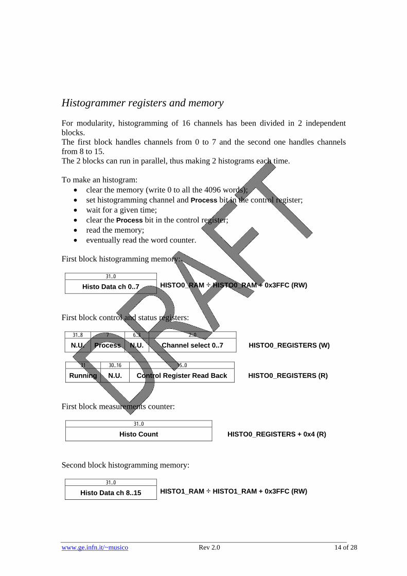
Histogrammer registers and memory For modularity, histogramming of 16 channels has been divided in 2 independent blocks. The first block handles channels from 0 to 7 and the second one handles channels from 8 to 15. The 2 blocks can run in parallel, thus making 2 histograms each time. To make an histogram:
clear the memory (write 0 to all the 4096 words); set histogramming channel and Process bit in the control register; wait for a given time; clear the Process bit in the control register; read the memory; eventually read the word counter.
First block histogramming memory:
31..0
Histo Data ch 0..7 HISTO0_RAM ÷ HISTO0_RAM + 0x3FFC (RW)
First block control and status registers:
31..8 7 6..3 2..0
N.U. Process N.U. Channel select 0..7 HISTO0_REGISTERS (W)
31 30..16 15..0
Running N.U. Control Register Read Back HISTO0_REGISTERS (R)
First block measurements counter:
31..0
Histo Count HISTO0_REGISTERS + 0x4 (R)
Second block histogramming memory:
31..0
Histo Data ch 8..15 HISTO1_RAM ÷ HISTO1_RAM + 0x3FFC (RW)
www.ge.infn.it/~musico Rev 2.0 15 of 28
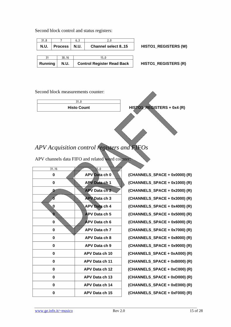
Second block control and status registers:
31..8 7 6..3 2..0
N.U. Process N.U. Channel select 8..15 HISTO1_REGISTERS (W)
31 30..16 15..0
Running N.U. Control Register Read Back HISTO1_REGISTERS (R)
Second block measurements counter:
31..0
Histo Count HISTO1_REGISTERS + 0x4 (R)
APV Acquisition control registers and FIFOs APV channels data FIFO and related word counter:
31..16 15..0
0 APV Data ch 0 (CHANNELS_SPACE + 0x0000) (R)
0 APV Data ch 1 (CHANNELS_SPACE + 0x1000) (R)
0 APV Data ch 2 (CHANNELS_SPACE + 0x2000) (R)
0 APV Data ch 3 (CHANNELS_SPACE + 0x3000) (R)
0 APV Data ch 4 (CHANNELS_SPACE + 0x4000) (R)
0 APV Data ch 5 (CHANNELS_SPACE + 0x5000) (R)
0 APV Data ch 6 (CHANNELS_SPACE + 0x6000) (R)
0 APV Data ch 7 (CHANNELS_SPACE + 0x7000) (R)
0 APV Data ch 8 (CHANNELS_SPACE + 0x8000) (R)
0 APV Data ch 9 (CHANNELS_SPACE + 0x9000) (R)
0 APV Data ch 10 (CHANNELS_SPACE + 0xA000) (R)
0 APV Data ch 11 (CHANNELS_SPACE + 0xB000) (R)
0 APV Data ch 12 (CHANNELS_SPACE + 0xC000) (R)
0 APV Data ch 13 (CHANNELS_SPACE + 0xD000) (R)
0 APV Data ch 14 (CHANNELS_SPACE + 0xE000) (R)
0 APV Data ch 15 (CHANNELS_SPACE + 0xF000) (R)

www.ge.infn.it/~musico Rev 2.0 16 of 28
31..16 15..0
0 Used Word ch 0 (CHANNELS_FLAGS) (R)
0 Used Word ch 1 (CHANNELS_FLAGS + 0x04) (R)
0 Used Word ch 2 (CHANNELS_FLAGS + 0x08) (R)
0 Used Word ch 3 (CHANNELS_FLAGS + 0x0C) (R)
0 Used Word ch 4 (CHANNELS_FLAGS + 0x10) (R)
0 Used Word ch 5 (CHANNELS_FLAGS + 0x14) (R)
0 Used Word ch 6 (CHANNELS_FLAGS + 0x18) (R)
0 Used Word ch 7 (CHANNELS_FLAGS + 0x1C) (R)
0 Used Word ch 8 (CHANNELS_FLAGS + 0x20) (R)
0 Used Word ch 9 (CHANNELS_FLAGS + 0x24) (R)
0 Used Word ch 10 (CHANNELS_FLAGS + 0x28) (R)
0 Used Word ch 11 (CHANNELS_FLAGS + 0x2C) (R)
0 Used Word ch 12 (CHANNELS_FLAGS + 0x30) (R)
0 Used Word ch 13 (CHANNELS_FLAGS + 0x34) (R)
0 Used Word ch 14 (CHANNELS_FLAGS + 0x38) (R)
0 Used Word ch 15 (CHANNELS_FLAGS + 0x3C) (R)
All APV Data ch x FIFO can be accessed from the given address for 1K words, to permit block transfers with auto increment on address lines. MSB of the Used Word registers is the corresponding FIFO Full flag, thus avoiding that if channel FIFO is full the corresponding Used Word is 0. In this release the FIFO size is 1024 words If DAQ MODE is 0x1, the readout data come form the APV frame decoder. If DAQ MODE is 0x3, the readout data come form the baseline subtractor and threshold cutter. Used Words and FIFO flags behave in the same way. If Event Building is enabled and the output SDRAM FIFO is not used, all the data must be read from Channel 0 addresses (Data FIFO, Used words and flags). Apv Readout Control and Status Registers:
31..16 15..0
FIFO FULL Flag FIFO EMPTY Flag CHANNELS_FLAGS + 0x40 (R)

www.ge.infn.it/~musico Rev 2.0 17 of 28
SYNCED ERROR CHANNELS_FLAGS + 0x44 (R)
FIFO EMPTY Flag & FIFO Full Flag = corresponding FIFO flag on READ side ERROR = FIFO Full Flag on WRITE side SYNCED = channel has sync pulses present All the preceding APV acquisition data space is used only for debug, since it is not mapped to a high speed data transfer space.
Pedestals and Thresholds RAMs Each RAM contains 128 12-bit pedestal values to be subtracted from the incoming APV data and threshold values to be compared with processed data. Before pedestal subtraction the COMMON OFFSET value is added to avoid negative numbers. These memories are dual port RAM shared with the channel processor FSMs. To read and write from these RAMs the corresponding channel must be disabled (ENABLE register bit cleared). If Pedestal value is 0xFFF the corresponding APV channel is not used in baseline computation. If Threshold value is 0xFFF the corresponding APV channel is always discarded from the output data set.
31..12 11..0
N.U. Pedestal APV 0 PEDESTAL_RAM ÷ PEDESTAL_RAM + 0x1FC) (RW)
N.U. Pedestal APV 1 (PEDESTAL_RAM + 0x200) ÷ (PEDESTAL_RAM + 0x3FC) (RW)
N.U. Pedestal APV 2 (PEDESTAL_RAM + 0x400) ÷ (PEDESTAL_RAM + 0x5FC) (RW))
N.U. Pedestal APV 3 (PEDESTAL_RAM + 0x600) ÷ (PEDESTAL_RAM + 0x7FC) (RW))
N.U. Pedestal APV 4 (PEDESTAL_RAM + 0x800) ÷ (PEDESTAL_RAM + 0x9FC) (RW)
N.U. Pedestal APV 5 (PEDESTAL_RAM + 0xA00) ÷ (PEDESTAL_RAM + 0xBFC) (RW))
N.U. Pedestal APV 6 (PEDESTAL_RAM + 0xC00) ÷ (PEDESTAL_RAM + 0xDFC) (RW))
N.U. Pedestal APV 7 (PEDESTAL_RAM + 0xE00) ÷ (PEDESTAL_RAM + 0xFFC) (RW)
N.U. Pedestal APV 8 (PEDESTAL_RAM + 0x1000) ÷ (PEDESTAL_RAM + 0x11FC) (RW)
N.U. Pedestal APV 9 (PEDESTAL_RAM + 0x1200) ÷ (PEDESTAL_RAM + 0x13FC) (RW)
N.U. Pedestal APV 10 (PEDESTAL_RAM + 0x1400) ÷ (PEDESTAL_RAM + 0x15FC) (RW)
N.U. Pedestal APV 11 (PEDESTAL_RAM + 0x1600) ÷ (PEDESTAL_RAM + 0x17FC) (RW)
N.U. Pedestal APV 12 (PEDESTAL_RAM + 0x1800) ÷ (PEDESTAL_RAM + 0x19FC) (RW)

www.ge.infn.it/~musico Rev 2.0 18 of 28
N.U. Pedestal APV 13 (PEDESTAL_RAM + 0x1A00) ÷ (PEDESTAL_RAM + 0x1BFC) (RW)
N.U. Pedestal APV 14 (PEDESTAL_RAM + 0x1C00) ÷ (PEDESTAL_RAM + 0x1DFC) (RW)
N.U. Pedestal APV 15 (PEDESTAL_RAM + 0x1E00) ÷ (PEDESTAL_RAM + 0x1FFC) (RW)
31..12 11..0
N.U. Threshold APV 0 THRESHOLD_RAM ÷ THRESHOLD_RAM + 0x1FC) (RW)
N.U. Threshold APV 1 (THRESHOLD_RAM + 0x200) ÷ (THRESHOLD_RAM + 0x3FC) (RW)
N.U. Threshold APV 2 (THRESHOLD_RAM + 0x400) ÷ (THRESHOLD_RAM + 0x5FC) (RW))
N.U. Threshold APV 3 (THRESHOLD_RAM + 0x600) ÷ (THRESHOLD_RAM + 0x7FC) (RW))
N.U. Threshold APV 4 (THRESHOLD_RAM + 0x800) ÷ (THRESHOLD_RAM + 0x9FC) (RW)
N.U. Threshold APV 5 (THRESHOLD_RAM + 0xA00) ÷ (THRESHOLD_RAM + 0xBFC) (RW))
N.U. Threshold APV 6 (THRESHOLD_RAM + 0xC00) ÷ (THRESHOLD_RAM + 0xDFC) (RW))
N.U. Threshold APV 7 (THRESHOLD_RAM + 0xE00) ÷ (THRESHOLD_RAM + 0xFFC) (RW)
N.U. Threshold APV 8 (THRESHOLD_RAM + 0x1000) ÷ (THRESHOLD_RAM + 0x11FC) (RW)
N.U. Threshold APV 9 (THRESHOLD_RAM + 0x1200) ÷ (THRESHOLD_RAM + 0x13FC) (RW)
N.U. Threshold APV 10 (THRESHOLD_RAM + 0x1400) ÷ (THRESHOLD_RAM + 0x15FC) (RW)
N.U. Threshold APV 11 (THRESHOLD_RAM + 0x1600) ÷ (THRESHOLD_RAM + 0x17FC) (RW)
N.U. Threshold APV 12 (THRESHOLD_RAM + 0x1800) ÷ (THRESHOLD_RAM + 0x19FC) (RW)
N.U. Threshold APV 13 (THRESHOLD_RAM + 0x1A00) ÷ (THRESHOLD_RAM + 0x1BFC) (RW)
N.U. Threshold APV 14 (THRESHOLD_RAM + 0x1C00) ÷ (THRESHOLD_RAM + 0x1DFC) (RW)
N.U. Threshold APV 15 (THRESHOLD_RAM + 0x1E00) ÷ (THRESHOLD_RAM + 0x1FFC) (RW)
Trigger Time FIFO The time between every incoming trigger pulse and the APV clock is measured and put into this FIFO. There are 2 implementation of TDC: a low resolution which uses the 240 MHz clock as LSB and a high resolution which is implemented usind a delay line. The chioce is done with TRIG_GEN_CONFIG[20]: 0 = low resolution, 1 = high resolution. The Trigger Time FIFO depth is 1024 word.
31 30 29..8 7..0

www.ge.infn.it/~musico Rev 2.0 19 of 28
FULL EMPTY N.U. Trigger Time CHANNELS_FLAGS + 0x60 (R)
SDRAM Chip Direct Access DDR2 SDRAM can be directly accessed using any A32D32 VME single and block cycles for test purposes at the SDRAM_BASE_ADDR for the following 8 Mbytes space. Setting SDRAM_BANK from 0 to 15 permit to access all the available 128 Mbytes (16 × 8 = 128). READOUT_CONFIG[15] must be cleared to access these spaces. To access the SDRAM this way, the user must write in the SDRAM_BASE_ADDR register the effective starting address (different from 0) shifted right by 2 positions. This address must not be in conflict with the following Output Buffer Space.
SDRAM output FIFO This is the main data output channel: it is possible to acecss it at full speed in any of the VME A32D32 read cycles or also A32D64 setting READOUT_CONFIG[14] = 1. Data are valid only if it is enabled (READOUT_CONFIG[15] = 1). To access the SDRAM FIFO output buffer, the user must write in the OBUF_BASE_ADDR register the effective starting address (different from 0) shifted right by 2 positions. This address must not be in conflict with the preceding SDRAM Direct Access Space. User must check the corresponding word count and flags before reading the data.

www.ge.infn.it/~musico Rev 2.0 20 of 28
Fiber interface The fiber optic interface is based on Aurora protocol adapting a single lane 2.5 Gb/s channel coming from Xilinx LogiCORE (see ref 11, 12). An additional layer has been devolped (by JLAB people) permitting a simpler access to the module, implementing a packet exchanging protocol as defined in JLAB environment. The MPD with this fiber interface is intended to be used with the SSP module (JLAB development) as master. Two data paths are implemented:
Configuration registers / RAM accesses Data readout
The configuration registers / RAM accesses path is a read-write channel that permits to access all the on-board resources defined here except the 8 registers mapped in the range 0x180 ÷ 0x19C. All the resources can be accesses with the same longword addresses:
longword_address = byte_address >> 2 The data readout path is a read only channel connected to the Event Builder output FIFO or to the SDRAM output FIFO. For testing purposes this channel can also be fed by a packet generator test module, controlled by IO_CONFIG_REGISTER upper bits. The module controlling the Event Builder data transfer transmit one block per data packet, issuing an EndOfPacket signal after the last word sent out. The fiber interface is enabled by default after power up, thus avoiding the need of VME accesses to configure it.

www.ge.infn.it/~musico Rev 2.0 21 of 28
FIR filters The converted analog data, before the processing, can be passed trough a FIR filter in order to mitigate the effect of the cable response (a sort of equalization). The filter coefficient are common for all the 16 channels and must be stored in the corresponding registersstarting from FIR_COEFFICIENTS address. The FIR filters have to be enabled setting the READOUT CONFIG[4] bit. The filters are implemented with the classical topology, using resource sharing, implemeting the scheme shown in the folowing figure.

www.ge.infn.it/~musico Rev 2.0 22 of 28
Implementation
FPGA BLOCK DIAGRAM
TRIGGER GENERATOR MODULE The Trigger Generator Module (TGM) generates pulses on the APV Trigger line. It has the following inputs:
Trigger and Fast Reset signals either coming from front panel LEMO connectors or backplane or software issued (via configuration register writing)
Trigger Mode bits form Configuration Register Reset and Calibration Latency values form Configuration Register Number of consecutive trigger form Configuration Register Signals form data FIFOs indicating possible congestions
and the following outputs:
APV Trigger line

www.ge.infn.it/~musico Rev 2.0 23 of 28
Number of missed trigger (received, but not sent to APVs) Busy line
The behaviour can be summarized as follows.
When TRIG MODE bits change from 0 to something different a ‘101’ pulse is generated to synchronize all the APVs. A ‘101’ pulse is also generated every correnponding incoming command (HW or SW).
If TRIG MODE = 1 a ‘100’ pulse is generated every rising edge of the corresponding incoming command (HW or SW). Pulses are sent out only if there is enough space to store at least a complete event in all the Frame Decoder output FIFOs. Pulses can be also stopped if the number of words in the DDR2 buffer is greater than a given value.
If TRIG MODE = 2 up to 15 ‘100’ pulses are sent to the APVs, as defined. TRIG MODE = 3 is a calibration mode. A ‘110’ pulse followed by up to 15
’100’ pulses are sent out. The delay from ‘110’ to ‘100’ is defined at the inputs.
The Number of missed trigger is cleared every ‘101’ APV trigger line sequence and incremented if a trigger pulse can be handled but there is no space in the FIFO to store data
The Busy line is activated if there is no space available in the data FIFO and the Mode bits are different from 0. The Busy line is also activated if the number of words in the DDR2 buffer is greater than a given value.
APV Trigger line ‘100’ pulses are generated only after the defined reset latency.
CHANNEL PROCESSOR MODULE They are 16 identical submodules, arranged in groups of 8 for modularity with the ADS5281. Each channels has the following inputs:
Enable bit from Control Register ADC output data stream Mode bits from configuration register FIFO Clear bit from configuration register Thresholds to identify logic ‘1’ and logic ‘0’ within the serial stream Pedestal & Threshold values Common Offset value FIFO read signal
and the following outputs:
Output data bus to the FIFO FIFO flags (empty, full) and number of used words

www.ge.infn.it/~musico Rev 2.0 24 of 28
FIFO attention signals, to be used by trigger module to avoid sending trigger out if there is not enough space.
If DAQ MODE = 2 the APV Frame Decoder block store ADC data into the output FIFO until it is full and restarts only when it is empty. If DAQ MODE = 1 or 2 data come out from the APV Frame Decoder block, while if DAQ MODE = 3 data come out from Threshold Cutter block. The APV Frame Decoder looks for the Frame Header (‘111’) and store 128 ADC data into its output FIFO together the header itself and a trailer word. A common offset is added to all 128 data and then the individual pedestal is subtracted: Output Data[i] = ADC Data[i] + Common Offset – Pedestal[i]. After the header has been identified the 128 values are written into the output FIFO only if there is enough space to store them. A counter is always incremented and stored in the trailer word, permitting to identify missed frames and to realign data (offline). While the 128 data are being written into the FIFO, the common mode noise is computed: the data are accumulated (if corresponding pedestal is not 0xFFF) and at the end the average value is calculated and written into the MEAN FIFO. If the MEAN FIFO is not empty a complete data set is present and the following block can start its processing. The Baseline Subtractor & Threshold Cutter block get data from the preceding stage. Its operations are:
Data Out[i] = Data In[i] – Common Mode Noise if( Data Out[i] > Threshold[i] ) write Data Out[i] to output
FIFO If Threshold[i] = 0xFFF the channel is not copied to the output (it is masked). Header & Trailer coming from preceding stage are always copied. An additional trailer is added for redundancy and easyness identifications of data. Data formats are reported in the block diagram.

www.ge.infn.it/~musico Rev 2.0 25 of 28
EVENT BUILDER MODULE This module puts together data coming out from the 16 Threshold Cutter blocks. The block diagram and behaviour is reported in the following picture.

www.ge.infn.it/~musico Rev 2.0 26 of 28
The output of the event builder can be read directly or can feed a large FIFO implemented using the on board 128 Mbytes DDR2 SDRAM. To read directly clear READOUT_CONFIG[15] (set to 0), while to use the large fifo set this bit to 1. If the DDR2 SDRAM output FIFO is not used, all the data must be read from Channel 0 addresses (Data FIFO, Used words and flags).

www.ge.infn.it/~musico Rev 2.0 27 of 28
SDRAM FIFO INTERFACE MODULE The output of the event builder can feed a large FIFO implemented using the on board 128 Mbytes DDR2 SDRAM. This module is quite complicated to guarantee a good througput and have flexibility in 32/64 bit readout. The data coming form the Event Builder are arranged on a 32 bit bounduary and then written into the SDRAM every 30 ns. Then the data are extracted from the SDRAM (every 20 ns), eventually arranged in 64 bit, and put in an output FIFO, needed for speedup the readout. The output FIFO is directly connected to the VME interface and can be accessed in any of the supported modes. Using SST320 a 64 bit word is extracted from the output FIFO every 30 ns (264 MB/s). With SST267 every 40 ns (225 MB/s). If the Fiber interface is used data goes directly to the output channel.

www.ge.infn.it/~musico Rev 2.0 28 of 28
References
1. ANSI/VITA 1-1994 “American National Standard for VME64” 2. ANSI/VITA 1.1-1997 “American National Standard for VME64 Extensions” 3. ANSI/VITA 23-1998 “American National Standard for VME64 Extensions for
Physics and Other Applications” 4. VITA 1.5-1999 “Draft Standard for Trial Use Approved bi the VITA Standards
Organization for the 2eSST” 5. ANSI/VITA 41.0-2006 “American National Standard for VXS VMEbus
Switched Serial Standard” 6. ALTERA “Arria GX Arria GX Device Handbook, Volume 1 & 2” 7. OpenCores, “I2C – Master Core Specification”, July 3, 2003, Rev 0.9 8. P. Musico, “VME64x Slave Interface IP Core Specifications”, Dec 1, 2005 9. Texas Instruments, ADS5281 Low power 8-channel, 12-bit, 50 MSPS ADC
with Serialized LVDS interface, web page: http://www.ti.com/product/ads5281 10. DELAY25 web page: http://proj-delay25.web.cern.ch/proj-delay25/delay25_-
_home.htm 11. Xilinx “LogiCORETM IP Aurora 8B/10B v5.3 User Guide”, UG353, Jan 18
2012 12. Xilinx “LogiCORE IP Aurora 8B/10B v5.3”, DS637, Jan 18 2012