Embed Size (px)
Citation preview
Freescale SemiconductorApplication Note
© Freescale Semiconductor, Inc., 2002, 2006. All rights reserved.
This application note describes how to take full advantage of the MPC8xx caches and MMU features to maximize system performance. It describes simple ways to measure system performance.
1 Memory Management UnitsThe MPC8xx uses one common space to map the program memory, data memory and peripherals. Therefore, it is necessary to differentiate various address space areas (pages) features. The main attributes to control are:
• Protection:
— Read/Write pages (data that can be modified), read-only pages (program or constant data), No Access pages (unmapped regions).
— Supervisor/User access pages. Some memory regions must be accessed only in supervisor mode.
— Guarded pages prevent speculative accesses to devices that are not well behaved, such as peripherals, FIFOs, and so on.
Contents
1 Memory Management Units . . . . . . . . . . . . . . . . . . . . .11.1 Basic MMU Features . . . . . . . . . . . . . . . . . . . . . . .21.2 Translation Disabled Versus Translation Enabled .61.3 Static Page Structure Versus Page on Demand . . . .7
2 Caches . . . . . . . . . . . . . . . . . . . . . . . . . . . . . . . . . . . . .102.1 Cache Basics . . . . . . . . . . . . . . . . . . . . . . . . . . . . .102.2 Cache Coherency . . . . . . . . . . . . . . . . . . . . . . . . .142.3 D-Cache Flush . . . . . . . . . . . . . . . . . . . . . . . . . . .152.4 Caching Permitted and Inhibited Regions . . . . . .162.5 Data/Instruction Lock in Caches . . . . . . . . . . . . . .162.6 Coding Practices Affecting Performance . . . . . . .17
3 Performance Estimation and Measurement . . . . . . . .193.1 Benchmarks . . . . . . . . . . . . . . . . . . . . . . . . . . . . .203.2 Cache Hit/Miss Ratio . . . . . . . . . . . . . . . . . . . . . .203.3 Instructions Per Clock . . . . . . . . . . . . . . . . . . . . . .25
MPC8xx Performance-Driven Optimization of Caches and MMU Configuration
Document Number: AN3066Rev. 1, 01/2006
MPC8xx Performance-Driven Optimization of Caches and MMU Configuration, Rev. 1
2 Freescale Semiconductor
Memory Management Units
• Caching:
— Caching permitted pages. Normal operation mode ensures the highest performance. Caching inhibited pages are used mainly to enforce coherency.
— Data cache (D-Cache) write through/copy back pages.
• Write tracing. Sometimes it is necessary to trace whether the data in a memory region was modified over a specified period of time–for example, when data stored on an external device (floppy disk, PCMCIA card) is temporarily transferred to the main memory. When such data is discarded, it must be copied back to the device only if it was modified.
Beside the assignment of memory attributes, the MPC8xx memory management units (MMUs) can be used for the following tasks:
• Create different user/supervisor memory spaces.
• Create up to 16 virtual address spaces.
• Relocate memory pages.
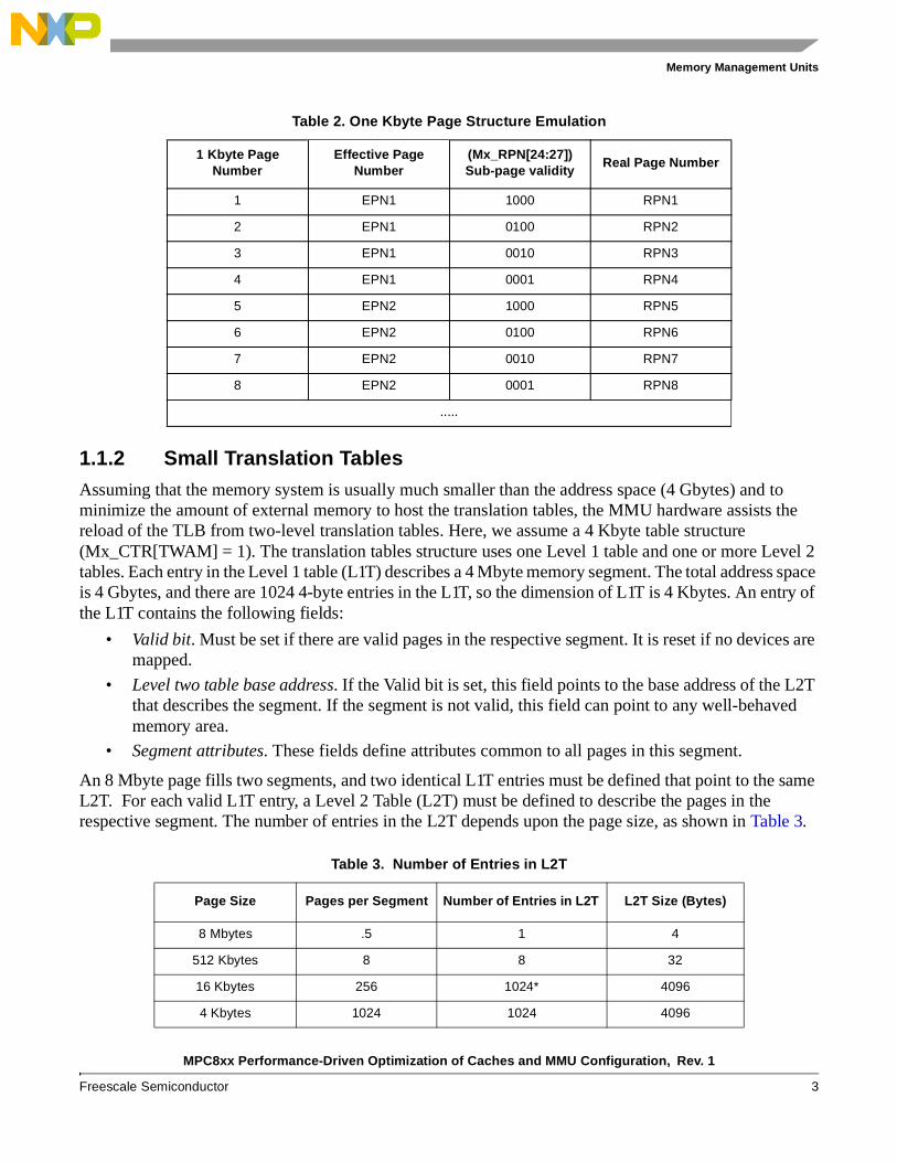
Each member of the MPC8xx family of communication controllers has two separate MMUs, one for instructions and another for data. Each MMU includes a translation lookaside buffer (TLB), which is a cache for the most recently used pages. Table 1 lists the available sizes of MMU, which depend on the number of TLB entries.
1.1 Basic MMU FeaturesThe MMUs are optimized for embedded applications, and features relevant to such applications are multiple page sizes, small translation tables, low power consumption, software tabletalk with hardware assistance, and lockable TLB entries.
1.1.1 Multiple Page SizesThe 8XX MMUs can handle pages sizes of 4 Kbytes, 16 Kbytes, 512 Kbytes, and 8 Mbytes. The 4 Kbyte pages can be divided into four 1 Kbyte sub-pages. The PPM bit in register Mx_CTR selects one of the two possible sub-page handling modes:
• 1 Kbyte protection. All four sub-pages are valid and each can have another protection mode.
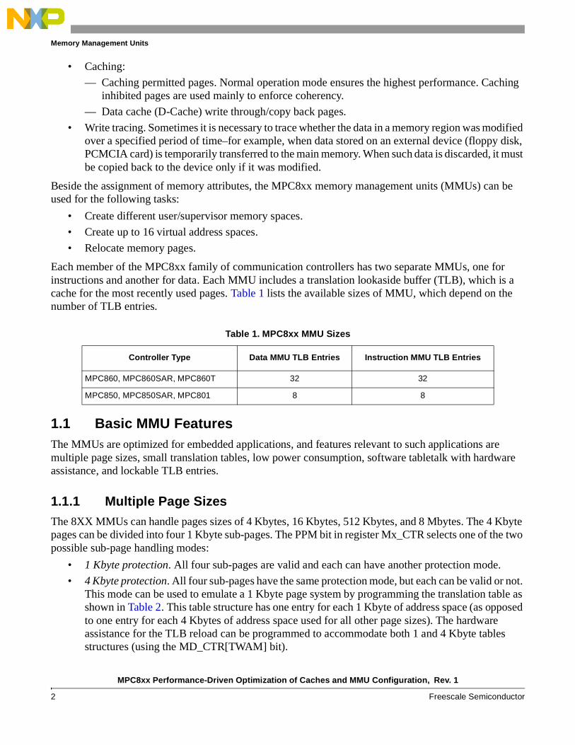
• 4 Kbyte protection. All four sub-pages have the same protection mode, but each can be valid or not. This mode can be used to emulate a 1 Kbyte page system by programming the translation table as shown in Table 2. This table structure has one entry for each 1 Kbyte of address space (as opposed to one entry for each 4 Kbytes of address space used for all other page sizes). The hardware assistance for the TLB reload can be programmed to accommodate both 1 and 4 Kbyte tables structures (using the MD_CTR[TWAM] bit).
Table 1. MPC8xx MMU Sizes
Controller Type Data MMU TLB Entries Instruction MMU TLB Entries
MPC860, MPC860SAR, MPC860T 32 32
MPC850, MPC850SAR, MPC801 8 8
MPC8xx Performance-Driven Optimization of Caches and MMU Configuration, Rev. 1
Freescale Semiconductor 3
Memory Management Units
1.1.2 Small Translation TablesAssuming that the memory system is usually much smaller than the address space (4 Gbytes) and to minimize the amount of external memory to host the translation tables, the MMU hardware assists the reload of the TLB from two-level translation tables. Here, we assume a 4 Kbyte table structure (Mx_CTR[TWAM] = 1). The translation tables structure uses one Level 1 table and one or more Level 2 tables. Each entry in the Level 1 table (L1T) describes a 4 Mbyte memory segment. The total address space is 4 Gbytes, and there are 1024 4-byte entries in the L1T, so the dimension of L1T is 4 Kbytes. An entry of the L1T contains the following fields:
• Valid bit. Must be set if there are valid pages in the respective segment. It is reset if no devices are mapped.
• Level two table base address. If the Valid bit is set, this field points to the base address of the L2T that describes the segment. If the segment is not valid, this field can point to any well-behaved memory area.
• Segment attributes. These fields define attributes common to all pages in this segment.
An 8 Mbyte page fills two segments, and two identical L1T entries must be defined that point to the same L2T. For each valid L1T entry, a Level 2 Table (L2T) must be defined to describe the pages in the respective segment. The number of entries in the L2T depends upon the page size, as shown in Table 3.
Table 2. One Kbyte Page Structure Emulation
1 Kbyte Page Number
Effective Page Number
(Mx_RPN[24:27]) Sub-page validity
Real Page Number
1 EPN1 1000 RPN1
2 EPN1 0100 RPN2
3 EPN1 0010 RPN3
4 EPN1 0001 RPN4
5 EPN2 1000 RPN5
6 EPN2 0100 RPN6
7 EPN2 0010 RPN7
8 EPN2 0001 RPN8
.....
Table 3. Number of Entries in L2T
Page Size Pages per Segment Number of Entries in L2T L2T Size (Bytes)
8 Mbytes .5 1 4
512 Kbytes 8 8 32
16 Kbytes 256 1024* 4096
4 Kbytes 1024 1024 4096
MPC8xx Performance-Driven Optimization of Caches and MMU Configuration, Rev. 1
4 Freescale Semiconductor
Memory Management Units
For each 16 Kbyte page, four identical entries must be defined in the L2T. Each entry in the L2T describes a page and contains a valid bit that must be set if the page is valid and that is reset if no devices are mapped, a real page number, and page attributes. Large page sizes save execution time and memory space. For example, a 32 Mbyte memory system can be mapped using 4 × 8 Mbyte pages or 8196 × 4 Kbyte pages:
• Execution time. For the first case, the four entries are loaded into the TLB during initialization or the first time the core accesses them. No further page miss exceptions are generated. The overhead in the second case can be estimated assuming, for example, that the core switches to a new 4 Kbyte page each 500 instructions and the probability that the new page is not represented by a TLB entry is 10 percent. For a 12 instruction TLB reload exception handler, the overhead is 0.24 percent.
• Memory space. In the first case, the translation tables take 4112 bytes (4096 for L1T and 4 × 4 for L2T); in the second case, they take 36864 bytes (4096 for L1T and 8 × 4096 for L2T), which is about nine times more.
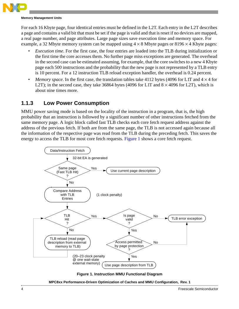
1.1.3 Low Power ConsumptionMMU power saving mode is based on the locality of the instruction in a program, that is, the high probability that an instruction is followed by a significant number of other instructions fetched from the same memory page. A logic block called fast TLB checks each core fetch request address against the address of the previous fetch. If both are from the same page, the TLB is not accessed again because all the information of the respective page was read from the TLB during the preceding fetch. This saves the energy to access the TLB for most core fetch requests. Figure 1 shows a core fetch request.
Figure 1. Instruction MMU Functional Diagram
Data/Instruction Fetch
Same page(Fast TLB Hit)
?
TLB Hit ?
TLB reload (read pagedescription from external
memory to TLB)
Use current page description
Yes
No
Yes
No
32-bit EA is generated
Compare Addresswith TLBEntries
Is pagevalid
?
Yes
NoTLB error exception
Access permitted by page protection
?
Yes
No
Use page description from TLB
(1 clock penalty)
(20–23 clock penalty@ one wait-stateexternal memory)
MPC8xx Performance-Driven Optimization of Caches and MMU Configuration, Rev. 1
Freescale Semiconductor 5
Memory Management Units
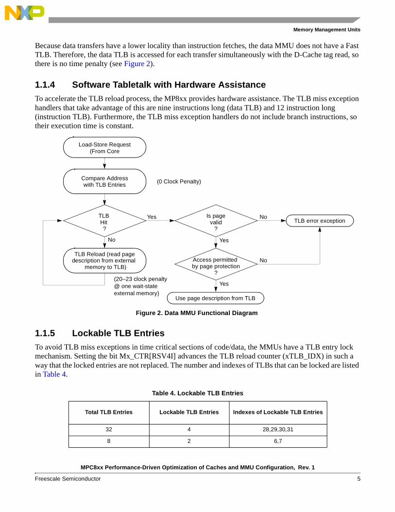
Because data transfers have a lower locality than instruction fetches, the data MMU does not have a Fast TLB. Therefore, the data TLB is accessed for each transfer simultaneously with the D-Cache tag read, so there is no time penalty (see Figure 2).
1.1.4 Software Tabletalk with Hardware AssistanceTo accelerate the TLB reload process, the MP8xx provides hardware assistance. The TLB miss exception handlers that take advantage of this are nine instructions long (data TLB) and 12 instruction long (instruction TLB). Furthermore, the TLB miss exception handlers do not include branch instructions, so their execution time is constant.
Figure 2. Data MMU Functional Diagram
1.1.5 Lockable TLB EntriesTo avoid TLB miss exceptions in time critical sections of code/data, the MMUs have a TLB entry lock mechanism. Setting the bit Mx_CTR[RSV4I] advances the TLB reload counter (xTLB_IDX) in such a way that the locked entries are not replaced. The number and indexes of TLBs that can be locked are listed in Table 4.
Table 4. Lockable TLB Entries
Total TLB Entries Lockable TLB Entries Indexes of Lockable TLB Entries
32 4 28,29,30,31
8 2 6,7
Load-Store Request
TLB Hit ?
TLB Reload (read pagedescription from external
memory to TLB)
Yes
No
Compare Addresswith TLB Entries
Is pagevalid
?
Yes
NoTLB error exception
Access permitted by page protection
?
Yes
No
Use page description from TLB
(0 Clock Penalty)
(20–23 clock penalty@ one wait-stateexternal memory)
(From Core
MPC8xx Performance-Driven Optimization of Caches and MMU Configuration, Rev. 1
6 Freescale Semiconductor
Memory Management Units
The tlbia instruction does not invalidate the locked entries. Two methods are available to invalidate a locked entry:
• Execute a tlbie instruction.
• Explicitly reset the valid field of the respective entry as shown in the following example:
addi r31,R0,0x1f00 # assume the entry no. 31 must be invalidated mtspr Mx_CTR,r31 # write the index to Mi_CTR or MD_CTR xor r31,r31,r31 # make r31 = 0 mtspr Mx_RPN,r31 # write an invalid entry
If necessary, the Mx_CTR and r31 registers must be saved/restored.
1.2 Translation Disabled Versus Translation EnabledThe MPC8xx powers up in translation disabled mode. Even if MMU functionality is not required in an application, enable them in order to boost performance. To use all its resources efficiently, the MPC8xx starts attempting to process instructions even before the program reaches a point where the instructions are part of the program flow. For example, if the instruction is from the address ADDR, the core may have fetched instructions from addresses ADDR+4, ADDR+8, and so on to have them ready for execution. This activity is speculative. If the instruction from the ADDR is a branch, the program flow changes and the instructions from the following addresses are discarded. However, if ADDR is the last instruction in a memory device and a peripheral or FIFO is mapped at ADDR + 4, the read cycle may have catastrophic results. To prevent such situation, the memory pages where these kinds of devices reside must be guarded.
If the MMUs are enabled (translation enabled), each page of memory can be guarded or not. The following rules apply for guarded pages:
• Speculative data load-stores stall until they are no longer speculative or are canceled by the core.
• All instruction fetches are prevented and generate an Instruction TLB Error exception.
If the MMUs are disabled (translation disabled), the whole memory is considered as guarded and the speculative accessed are treated as follows:
• Speculative data load-stores stall until they are no longer speculative or are canceled by the core.
• All speculative instruction fetches outside the current real mode page are stalled till they are no longer speculative or are canceled by the core. The real mode page length is given in Table 5.
The effect of the stalled accesses can be significant. If a code sequence contains only load-store instructions that hit the cache, the number of instructions per clock is close to 1 in a non-guarded page and close to 0.5 in a guarded page (or when the translation is disabled). Also, the sequencer stalls (when the translation is disabled) for several clock cycles each time a real page boundary is crossed. Table 6 summarizes the effect of guarded storage.
Table 5. MPC8xx Real Mode Page Length
MI_CTR[PPM] Real Page Length (Kbytes)
0 4
1 1
MPC8xx Performance-Driven Optimization of Caches and MMU Configuration, Rev. 1
Freescale Semiconductor 7
Memory Management Units
1.3 Static Page Structure Versus Page on DemandAn application can load the MMUs in two ways:
• Page on demand. A page descriptor is loaded into a TLB entry for a translation of an address from the respective page.
• Static page structure. All page descriptors in an application are loaded into the TLB during initialization.
Static page structure is preferable because it saves the overhead of the TLB miss interrupts and the external memory necessary to host the translation tables. Since the MPC8xx has large page sizes (up to 8 Mbytes), this strategy can be implemented for a wide range of applications.
A TLB entry consists of a CAM entry and a RAM entry. To load a TLB entry, a mtspr Mx_RPN,reg must be performed. The TLB entry to which the Mx_CTR[xTLB_INDX] points is updated using information from the Mx_EPN, Mx_TWC, and Mx_RPN registers. Part of this information is stored in the CAM for use by the TLB hit/miss logic, and the rest is stored in the RAM and for use by the translation logic. The TLB includes multiple hit prevention. When a new entry is loaded, it is checked against previously loaded entries. The existing page is invalidated if a potential multiple hit is detected because the new page overlaps an existing page and is shared or not shared and has the same ASID:
• Effective Address (according to the page size)
• Sub-page index (if Mx_CTR[PPCS] = 0)
• MSR[[PR] (if Mx_CTR[PPCS] = 1)
• M_CASID[CASID] if the SH bit in the CAM entry is reset.
If no CAM entry hits, a TLB miss exception is generated. For a hit, the respective RAM entry is read and the protection bits are checked. For a protection violation, a TLB error is generated; otherwise, the translation is performed.
The TLB entries are not invalidated at power-up reset, so a tlbia instruction must be executed before they are loaded. Care must be taken not to set the Mx_CTR[RSV4I] bit before this instruction executes because it prevents invalidation of the locked entries.
Beside loading the TLBs with page descriptors, other MMU mechanisms must be initialized:
• Default cache attributes. The Mx_CTR[CIDEF] bits inhibit caching and the MD_CTR[WTDEF] forces write-through mode of the D-Cache while the translation is inhibited.
Table 6. Effect of Guarded Storage
Type of Speculative Transfer
Translation Disabled (TD) Translation Enabled (TE) Highest Expected
Performance Penalty (TD/TE)
Load-store Stalled Stalled only if the current page is guarded
.5
Fetch Stalled if from another
real page than the current one
Protection error .95
MPC8xx Performance-Driven Optimization of Caches and MMU Configuration, Rev. 1
8 Freescale Semiconductor
Memory Management Units
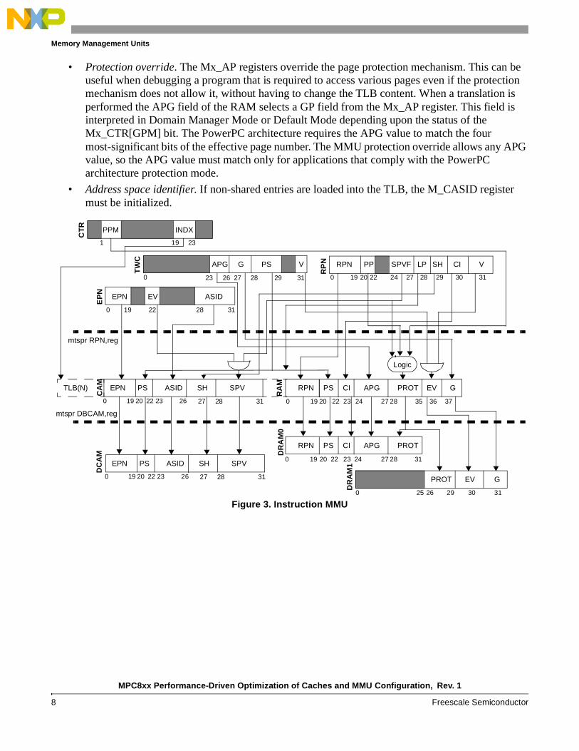
• Protection override. The Mx_AP registers override the page protection mechanism. This can be useful when debugging a program that is required to access various pages even if the protection mechanism does not allow it, without having to change the TLB content. When a translation is performed the APG field of the RAM selects a GP field from the Mx_AP register. This field is interpreted in Domain Manager Mode or Default Mode depending upon the status of the Mx_CTR[GPM] bit. The PowerPC architecture requires the APG value to match the four most-significant bits of the effective page number. The MMU protection override allows any APG value, so the APG value must match only for applications that comply with the PowerPC architecture protection mode.
• Address space identifier. If non-shared entries are loaded into the TLB, the M_CASID register must be initialized.
Figure 3. Instruction MMU
PPM INDX
CT
R
1 19 23
APG G VPS
TW
C
RP
N RPN PP SPVF LP SH CI V
23 26 27 28 29 31
EP
N
EPN EV ASID
EPN PS ASID SH SPV
0 19 20 22 23 26 27 28 31
EPN PS ASID SH SPV
0 19 20 22 23 26 27 28 31
TLB(N)
CA
MD
CA
M
RA
M
RPN PS CI APG PROT EV G
DR
AM
0
RPN PS CI APG PROT
PROT EV G
0
0
0
19 20 22 23 24 27 28 35 36 37
DR
AM
1
19 20 22 23 24 27 28 31
25 26 29 30 31
0 19 22 28 31
00 19 20 22 24 27 28 29 30 31
mtspr RPN,reg
mtspr DBCAM,reg
Logic
MPC8xx Performance-Driven Optimization of Caches and MMU Configuration, Rev. 1
Freescale Semiconductor 9
Memory Management Units
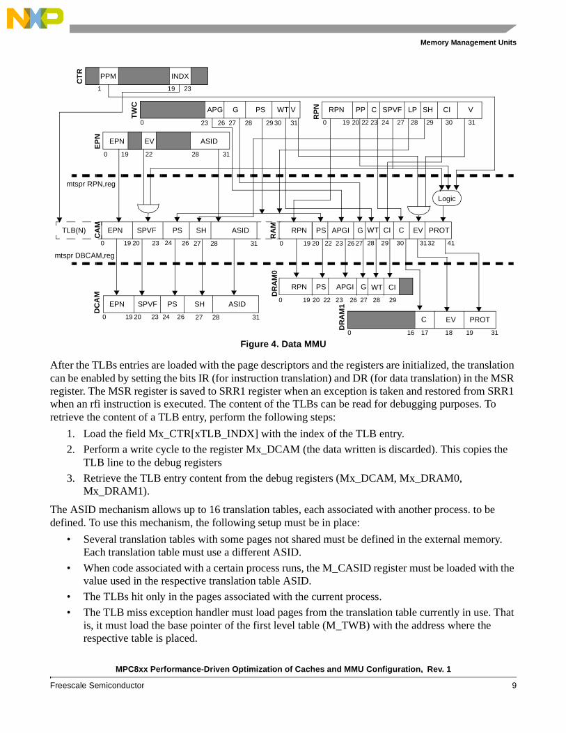
Figure 4. Data MMU
After the TLBs entries are loaded with the page descriptors and the registers are initialized, the translation can be enabled by setting the bits IR (for instruction translation) and DR (for data translation) in the MSR register. The MSR register is saved to SRR1 register when an exception is taken and restored from SRR1 when an rfi instruction is executed. The content of the TLBs can be read for debugging purposes. To retrieve the content of a TLB entry, perform the following steps:
1. Load the field Mx_CTR[xTLB_INDX] with the index of the TLB entry.
2. Perform a write cycle to the register Mx_DCAM (the data written is discarded). This copies the TLB line to the debug registers
3. Retrieve the TLB entry content from the debug registers (Mx_DCAM, Mx_DRAM0, Mx_DRAM1).
The ASID mechanism allows up to 16 translation tables, each associated with another process. to be defined. To use this mechanism, the following setup must be in place:
• Several translation tables with some pages not shared must be defined in the external memory. Each translation table must use a different ASID.
• When code associated with a certain process runs, the M_CASID register must be loaded with the value used in the respective translation table ASID.
• The TLBs hit only in the pages associated with the current process.
• The TLB miss exception handler must load pages from the translation table currently in use. That is, it must load the base pointer of the first level table (M_TWB) with the address where the respective table is placed.
PPM INDXC
TR
1 19 23
APG G WT VPS
TW
C
RP
N RPN PP SPVF LP SH CI V
23 26 27 28 29 31
EP
N
EPN EV ASID
EPN ASIDSH
0 19 20 23 26 27 28 31
EPN ASIDSHSPVF
0 19 20 23 26 27 28 31
TLB(N)
CA
MD
CA
M
RA
M
RPN PS APGI PROTEVG
DR
AM
0
RPN PS APGI G
PROTEV
0
0
0
19 20 22 23 26 27 29 30 31 41
DR
AM
1
19 20 22 23 26 27 28 29
16 17 18 19 31
0 19 22 28 31
00 19 20 22 24 27 28 29 30 31
mtspr RPN,reg
mtspr DBCAM,reg
Logic
30
C
23
SPVF PS
PS
24 C
WT CI
WT CI C
28 3224
MPC8xx Performance-Driven Optimization of Caches and MMU Configuration, Rev. 1
10 Freescale Semiconductor
Caches
2 CachesThe MPC8xx core can process close to one instruction per clock. This rate cannot be sustained because of limited memory system bandwidth. To overcome this limitation, two caches (one for instructions and one for data) provide the core a faster access to the most recently used instructions and data. As long as the fetch and load/store requests find the respective instructions and data in the caches (cache hit) the core can maintain the close to one instruction per clock rate. If the instruction or data are not in the caches (cache miss), they must be transferred from the external memory system, with a delay of several clocks (cache miss penalty) that slows down program execution.
In a system with an 80 percent cache hit ratio and a 5 clock cache miss penalty, the overall slow-down of the system caused by the cache misses is 1.8 times ((20 × 5 + 80) / 100). An improvement of only 5 percent in the hit ratio reduces this penalty to 1.6 times—a 12 percent performance improvement. In a system that transfers significant amounts of data between the CPM and the memory system, the average cache miss latency increases because the external bus is not always available for cache initiated transfers. Therefore, the performance impact of the cache misses is even higher.
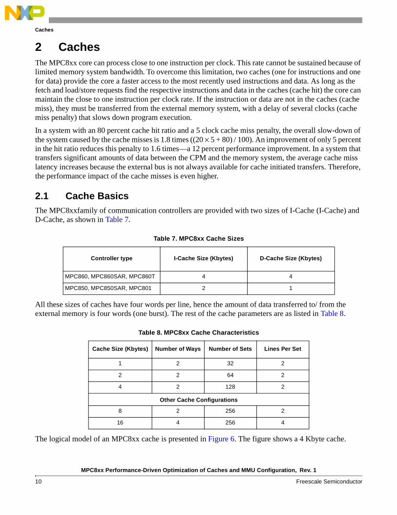
2.1 Cache BasicsThe MPC8xxfamily of communication controllers are provided with two sizes of I-Cache (I-Cache) and D-Cache, as shown in Table 7.
All these sizes of caches have four words per line, hence the amount of data transferred to/ from the external memory is four words (one burst). The rest of the cache parameters are as listed in Table 8.
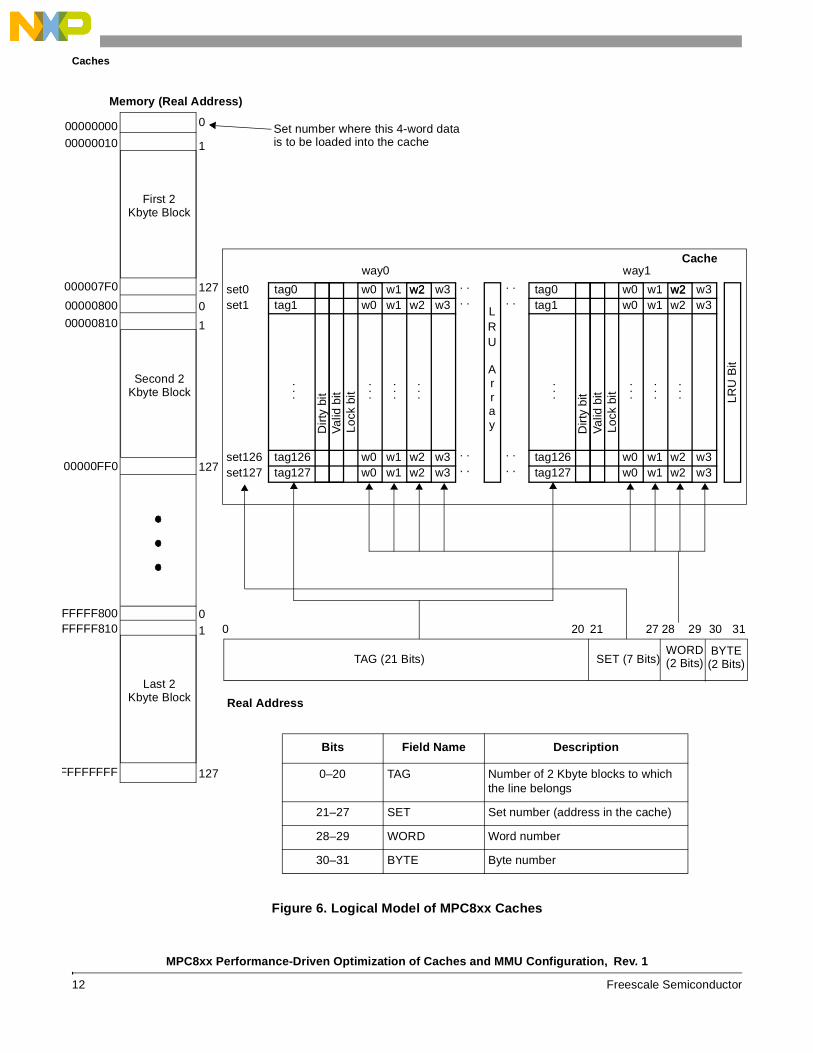
The logical model of an MPC8xx cache is presented in Figure 6. The figure shows a 4 Kbyte cache.
Table 7. MPC8xx Cache Sizes
Controller type I-Cache Size (Kbytes) D-Cache Size (Kbytes)
MPC860, MPC860SAR, MPC860T 4 4
MPC850, MPC850SAR, MPC801 2 1
Table 8. MPC8xx Cache Characteristics
Cache Size (Kbytes) Number of Ways Number of Sets Lines Per Set
1 2 32 2
2 2 64 2
4 2 128 2
Other Cache Configurations
8 2 256 2
16 4 256 4
MPC8xx Performance-Driven Optimization of Caches and MMU Configuration, Rev. 1
Freescale Semiconductor 11
Caches
A D-Cache access cycle begins with a request from the core load-store unit for a data transfer. An I-Cache cycle begins with a request from the core sequencer for an instruction fetch. If the cache contains the respective data/instruction (cache hit), it serves the request in one clock (zero wait state). For a cache miss, the cache initiates a burst transfer from/to the external bus. The main cache performance features are as follows:
• Critical word first external memory accesses. During a miss, the external memory transfer initiated by the cache begins with the word required to complete the core request. The burst advances and then brings the other three words (burst tail).
• Block operation. Cache operation is blocked for a miss until the critical word is delivered to the core. The cache miss penalty equals the first burst beat latency plus one clock.
• Hit under miss. After the critical word is transferred, the cache can serve other core requests while the burst tail is transferred.
• Stream hit. The cache can hit in the burst tail, even before the burst tail is actually written into the array.
• Line lock implementation-specific command. The data inside the caches can be locked on a per line granularity, thus creating a hit certainty for critical code/data.
• Flush by cache location. The D-Cache lines are flushed using their cache address (set/way number).
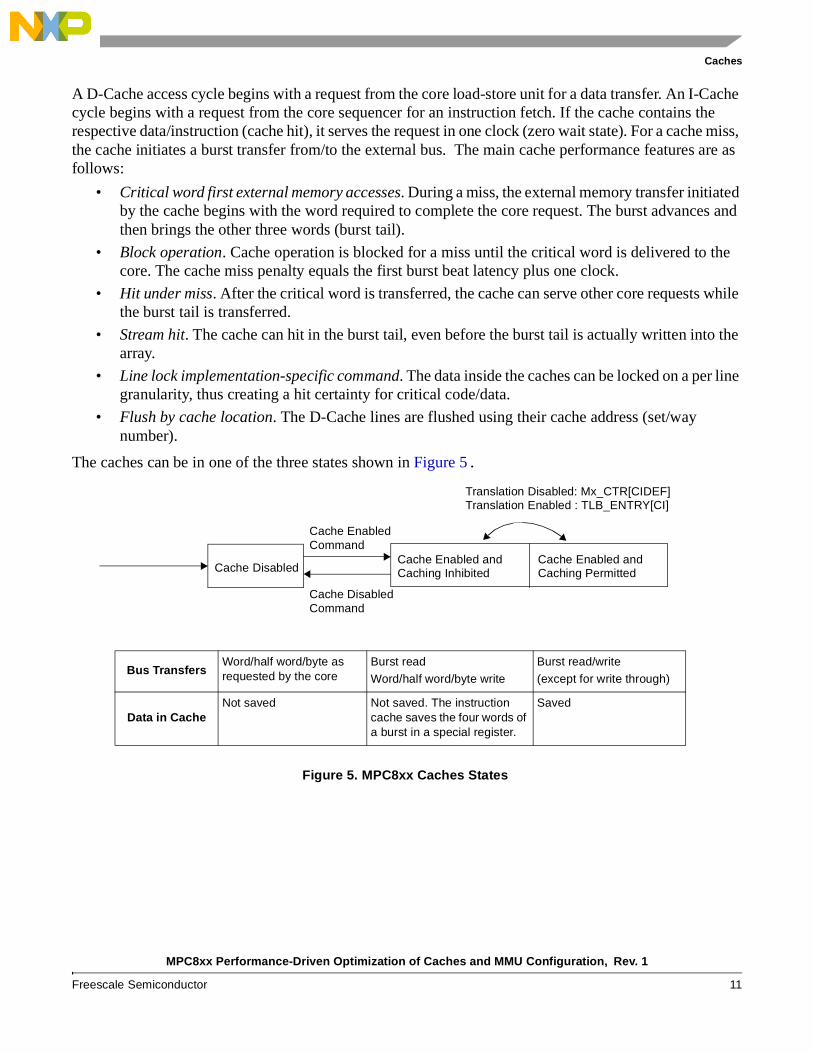
The caches can be in one of the three states shown in Figure 5.
Figure 5. MPC8xx Caches States
Cache DisabledCache Enabled andCaching Inhibited
Cache Enabled andCaching Permitted
Cache Enabled Command
Cache Disabled Command
Translation Disabled: Mx_CTR[CIDEF]Translation Enabled : TLB_ENTRY[CI]
Bus TransfersWord/half word/byte as requested by the core
Burst read
Word/half word/byte write
Burst read/write
(except for write through)
Data in CacheNot saved Not saved. The instruction
cache saves the four words of a burst in a special register.
Saved
MPC8xx Performance-Driven Optimization of Caches and MMU Configuration, Rev. 1
12 Freescale Semiconductor
Caches
Figure 6. Logical Model of MPC8xx Caches
way0. .. .
. .
. .
set0set1
set127set126
tag0 w0 w1 w2 w3
Val
id b
itLo
ck b
it
tag1 w0 w1 w2 w3
tag127 w0 w1 w2 w3tag126 w0 w1 w2 w3
. . .
. . .
. . .
. . .
LRU
Array
. .
. .
. .
. .
w2 tag0 w0 w1 w2 w3
way1
tag1 w0 w1 w2 w3
tag127 w0 w1 w2 w3tag126 w0 w1 w2 w3
. . .
. . .
. . .
. . .
Val
id b
itLo
ck b
it
w2
Dirt
y bi
t
Dirt
y bi
t
Cache
LRU
Bit
20 21
SET (7 Bits)WORD(2 Bits)
BYTE(2 Bits)TAG (21 Bits)
0 27 28 29 30 31
Real Address
Memory (Real Address)
First 2Kbyte Block
00000000 0
1
Second 2Kbyte Block
Last 2Kbyte Block
00000010
000007F0
00000800
00000810
00000FF0
FFFFF800FFFFF810
FFFFFFFF
127
0
1
127
01
127
Set number where this 4-word datais to be loaded into the cache
Bits Field Name Description
0–20 TAG Number of 2 Kbyte blocks to which the line belongs
21–27 SET Set number (address in the cache)
28–29 WORD Word number
30–31 BYTE Byte number
MPC8xx Performance-Driven Optimization of Caches and MMU Configuration, Rev. 1
Freescale Semiconductor 13
Caches
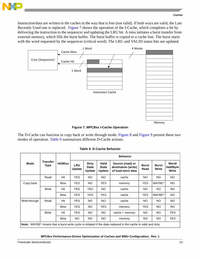
Instruction/data are written to the caches in the way that is free (not valid). If both ways are valid, the Last Recently Used one is replaced. Figure 7 shows the operation of the I-Cache, which completes a hit by delivering the instruction to the sequencer and updating the LRU bit. A miss initiates a burst transfer from external memory, which fills the burst buffer. The burst buffer is copied to a cache line. The burst starts with the word requested by the sequencer (critical word). The LRU and VALID status bits are updated.
Figure 7. MPC8xx I-Cache Operation
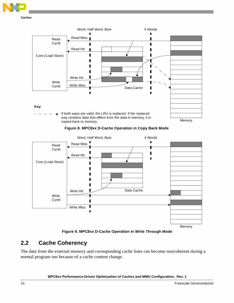
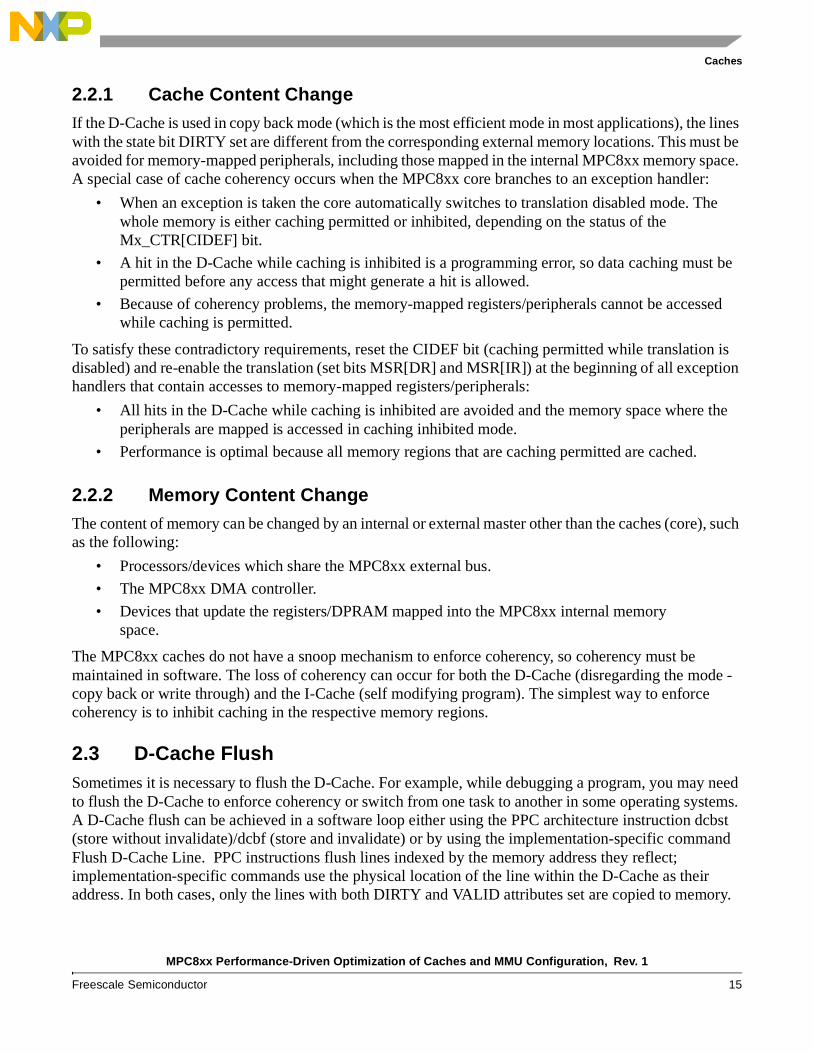
The D-Cache can function in copy back or write through mode. Figure 8 and Figure 9 present these two modes of operation. Table 9 summarizes different D-Cache actions.
Table 9. D-Cache Behavior
Mode Transfer
Type Hit/Miss
Behavior
LRU Update
Dirty State
Update
Valid State
Update
Source (read) or destination (write) of load-store data
Burst Read
Burst Write
Word/ Half/Byte
Write
Read Hit YES NO NO cache NO NO NO
Copy back Miss YES NO YES memory YES MAYBE* NO
Write Hit YES YES NO cache NO NO NO
Miss YES YES YES cache YES MAYBE* NO
Write through Read Hit YES NO NO cache NO NO NO
Miss YES NO YES memory YES NO NO
Write Hit YES NO NO cache + memory NO NO YES
Miss NO NO NO memory NO NO YES
Note: MAYBE* means that a burst write cycle is initiated if the data replaced in the cache is valid and dirty.
Core (Sequencer)
Cache Miss
Cache Hit
Memory
Instruction Cache
1 Word 4 Words
1 Word
MPC8xx Performance-Driven Optimization of Caches and MMU Configuration, Rev. 1
14 Freescale Semiconductor
Caches
Figure 8. MPC8xx D-Cache Operation in Copy Back Mode
Figure 9. MPC8xx D-Cache Operation in Write Through Mode
2.2 Cache CoherencyThe data from the external memory and corresponding cache lines can become noncoherent during a normal program run because of a cache content change.
Core (Load-Store)
Read Miss
Read Hit
Memory
Data Cache
ReadCycle
WriteCycle
Write Hit
Write Miss
Word, Half Word, Byte 4 Words
Key:
If both ways are valid, the LRU is replaced. If the replacedway contains data that differs from the data in memory, it iscopied back to memory.
Core (Load-Store)
Read Miss
Read Hit
Memory
Data Cache
ReadCycle
WriteCycle
Write Hit
Write Miss
Word, Half Word, Byte 4 Words
MPC8xx Performance-Driven Optimization of Caches and MMU Configuration, Rev. 1
Freescale Semiconductor 15
Caches
2.2.1 Cache Content ChangeIf the D-Cache is used in copy back mode (which is the most efficient mode in most applications), the lines with the state bit DIRTY set are different from the corresponding external memory locations. This must be avoided for memory-mapped peripherals, including those mapped in the internal MPC8xx memory space. A special case of cache coherency occurs when the MPC8xx core branches to an exception handler:
• When an exception is taken the core automatically switches to translation disabled mode. The whole memory is either caching permitted or inhibited, depending on the status of the Mx_CTR[CIDEF] bit.
• A hit in the D-Cache while caching is inhibited is a programming error, so data caching must be permitted before any access that might generate a hit is allowed.
• Because of coherency problems, the memory-mapped registers/peripherals cannot be accessed while caching is permitted.
To satisfy these contradictory requirements, reset the CIDEF bit (caching permitted while translation is disabled) and re-enable the translation (set bits MSR[DR] and MSR[IR]) at the beginning of all exception handlers that contain accesses to memory-mapped registers/peripherals:
• All hits in the D-Cache while caching is inhibited are avoided and the memory space where the peripherals are mapped is accessed in caching inhibited mode.
• Performance is optimal because all memory regions that are caching permitted are cached.
2.2.2 Memory Content ChangeThe content of memory can be changed by an internal or external master other than the caches (core), such as the following:
• Processors/devices which share the MPC8xx external bus.
• The MPC8xx DMA controller.
• Devices that update the registers/DPRAM mapped into the MPC8xx internal memoryspace.
The MPC8xx caches do not have a snoop mechanism to enforce coherency, so coherency must be maintained in software. The loss of coherency can occur for both the D-Cache (disregarding the mode - copy back or write through) and the I-Cache (self modifying program). The simplest way to enforce coherency is to inhibit caching in the respective memory regions.
2.3 D-Cache FlushSometimes it is necessary to flush the D-Cache. For example, while debugging a program, you may need to flush the D-Cache to enforce coherency or switch from one task to another in some operating systems. A D-Cache flush can be achieved in a software loop either using the PPC architecture instruction dcbst (store without invalidate)/dcbf (store and invalidate) or by using the implementation-specific command Flush D-Cache Line. PPC instructions flush lines indexed by the memory address they reflect; implementation-specific commands use the physical location of the line within the D-Cache as their address. In both cases, only the lines with both DIRTY and VALID attributes set are copied to memory.
MPC8xx Performance-Driven Optimization of Caches and MMU Configuration, Rev. 1
16 Freescale Semiconductor
Caches
To flush a line from the D-Cache using the implementation-specific command, the DC_ADR register must be set (DC_ADR[way] = way number, DC_ADR[set] = set number of the line to be flushed). Then the Flush D-Cache Line command must be issued by writing a value of 0xE into the DC_CTR[4:7] field.
2.4 Caching Permitted and Inhibited RegionsFor best performance, minimize the use of caching inhibited mode in both time and space:
• Minimize time by enabling the caches as early as possible in the initialization code and than avoiding disabling them.
• Minimize space by limiting the caching inhibited memory regions to those necessary for maintaining coherency.
To enable the caches, the implementation-specific commands must be issued because the caches are not initialized by reset:
• Unlock all
• Invalidate all
• D-Cache/I-Cache enable
2.5 Data/Instruction Lock in CachesTo guarantee cache hits for critical segments of a program, such as an interrupt handler that must be completed as quickly as possible, lock data/instructions in the caches. Both the D-Cache and I-Cache include mechanisms to lock their content on a line granularity using implementation-specific commands. Locked lines operate as zero wait-state SRAM; they are not replaced during misses and are not affected by invalidate commands. While a portion of the cache content is locked, the performance increase in the execution of the locked instructions/data must be weighed against the performance loss in the rest of the program. For example, for a 4Kbyte/2way cache certain compromises are necessary:
• If the amount of cache to be locked is smaller than one way, place the code/data in the same way. Locking both ways of a set creates 16-byte caching inhibited areas, each consuming 2 Kbytes of memory and therefore bottlenecks.
• When one way is (almost) completely locked, the rest of the code still uses the second way and the cache becomes a 2 Kbyte/1 way cache that still provides fair performance.
• When almost all the cache is locked (both ways), the rest of the code runs as in caching inhibited mode. The performance penalty is significant. An easier solution that has the same effect is to program the critical code in the MMU as caching permitted and the rest as caching inhibited. This method can also be used if the critical code is slightly larger than the cache to ensure it is not replaced by the noncritical code.
The D-Cache and I-Cache are locked in different ways. For both caches, implementation-specific commands are provided to unlock a certain line (addressed by its physical location within the cache) and all the locked lines. To unlock a line, load its address in IC_ADR / DC_ADR (way number and set number) and then issue an Unlock Line command using the IC_CST / DC_CST register.
MPC8xx Performance-Driven Optimization of Caches and MMU Configuration, Rev. 1
Freescale Semiconductor 17
Caches
2.5.1 D-Cache Line LockTo lock a number of lines in the D-Cache, perform the following steps:
1. Read the DC_CST register to reset the sticky error bits.
2. Write the real address of the line to be locked to the DC_ADR register.
3. Sync.
4. Issue the Lock Line command to the DC_CST register (16 bytes are transferred from the memory to the D-Cache and the LOCK and VALID status bits of the respective line are set).
5. Return to step 2 to lock more lines.
6. Sync.
7. Read the DC_CST register and check the bit CCER2. If this bit is reset, the operation completed without error.
2.5.2 I-Cache Line Load and LockTo lock a number of lines in the I-Cache, perform the following steps:
1. Read the IC_CST register to reset the sticky error bits.
2. Write the real address of the line to be locked to the IC_ADR register.
3. Issue the Load and Lock Line command to the IC_CST register (16 bytes are transferred from the memory to the I-Cache and the LOCK and VALID status bits of the respective line are set).
4. Sync.
5. Return to step 2 to lock more lines.
6. Sync.
7. Read the IC_CST register and check the CCER1, CCER2, and CCER3 bits. If these bits are all reset, the operation completed without error.
2.6 Coding Practices Affecting PerformanceSome coding practices can significantly affect the performances of an application. This section discusses practices relevant to the PowerPC architecture in general and the MPC8xx family in particular.
2.6.1 Optimize Memory TransfersA memory transfer requires roughly the same amount of time for one byte, one half-word, or one word. Therefore, use word transfers as much as possible.
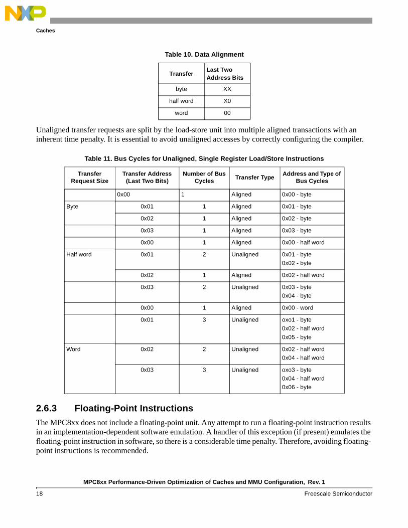
2.6.2 Data AlignmentThe MPC8xx performs only naturally aligned accesses, as shown in Table 10.
MPC8xx Performance-Driven Optimization of Caches and MMU Configuration, Rev. 1
18 Freescale Semiconductor
Caches
Unaligned transfer requests are split by the load-store unit into multiple aligned transactions with an inherent time penalty. It is essential to avoid unaligned accesses by correctly configuring the compiler.
2.6.3 Floating-Point InstructionsThe MPC8xx does not include a floating-point unit. Any attempt to run a floating-point instruction results in an implementation-dependent software emulation. A handler of this exception (if present) emulates the floating-point instruction in software, so there is a considerable time penalty. Therefore, avoiding floating- point instructions is recommended.
Table 10. Data Alignment
Transfer Last Two Address Bits
byte XX
half word X0
word 00
Table 11. Bus Cycles for Unaligned, Single Register Load/Store Instructions
Transfer Request Size
Transfer Address (Last Two Bits)
Number of Bus Cycles Transfer Type
Address and Type of Bus Cycles
0x00 1 Aligned 0x00 - byte
Byte 0x01 1 Aligned 0x01 - byte
0x02 1 Aligned 0x02 - byte
0x03 1 Aligned 0x03 - byte
0x00 1 Aligned 0x00 - half word
Half word 0x01 2 Unaligned 0x01 - byte
0x02 - byte
0x02 1 Aligned 0x02 - half word
0x03 2 Unaligned 0x03 - byte
0x04 - byte
0x00 1 Aligned 0x00 - word
0x01 3 Unaligned oxo1 - byte
0x02 - half word
0x05 - byte
Word 0x02 2 Unaligned 0x02 - half word
0x04 - half word
0x03 3 Unaligned oxo3 - byte
0x04 - half word
0x06 - byte
MPC8xx Performance-Driven Optimization of Caches and MMU Configuration, Rev. 1
Freescale Semiconductor 19
Performance Estimation and Measurement
2.6.4 InliningIn the MPC8xx, the sequencer executes the branch instructions. It can issue one sequential instruction to the execution units each clock, if all necessary resources are available, and process the branch instructions in parallel as long as they do not come in pairs. Therefore, the execution time of an inlined subroutine may not be considerably shorter than the execution time of the subroutine plus two branch instructions. Furthermore, if inlining subroutines increases the length of a loop so that it no longer fits into the I-Cache, the hit ratio decreases and also overall system performance. Use inlining with caution and when a profiling tool indicates that it might improve performance.
2.6.5 PredictionThe sequencer fetches instructions in advance (speculatively). Conditional branches with the condition not yet available are predicted according to the Y bit from the BO field of the opcode. The prefetch mechanism continues on the predicted path until the condition is evaluated. If the wrong path is followed (misprediction), the mispredicted instructions are discarded. This might empty the sequencer prefetch queue and stall the instruction issue process till instructions on the correct path are fetched. To optimize performance, the conditions of the conditional branches must be available as early as possible and the Y bit must be set to point to the most probable path.
2.6.6 Development SupportThe MPC8xx family includes extensive development support. To provide visibility of the program flow, the following mechanisms slow down execution speed:
• Serialized mode
• Show cycles
When the development mechanisms are no longer necessary, disable them to get the highest possible performance. To disable the serialized mode and the show cycles, write a value of 0x7 into the ISCT_SER field of the ICTRL register.
3 Performance Estimation and MeasurementDuring the early stages of application development when a hardware platform must be selected, system performance must be estimated to avoid a costly over-powered design or an under-powered one that does not meet the requirements. During the software development cycle, system performance must be measured and compared with the estimated value. Less than estimated performance might indicate deficiencies in the way processor resources are used.
Performance of a processor can be estimated in an application starting from the core performance (for example, MIPS) amended by the cache miss penalty. The cache miss penalty can be estimated as the product of the cache miss ratio and the cache miss latency. The cache miss ratio depends upon the code and the cache(s) sizes and organization. It can be estimated by simulating or running a similar application or portion of an application on a development system. The cache miss latency depends upon the number of wait states of the memory system and the internal latency. For example, consider a system with the following properties:
MPC8xx Performance-Driven Optimization of Caches and MMU Configuration, Rev. 1
20 Freescale Semiconductor
Performance Estimation and Measurement
• IPC0 (number of instructions per cycle at a 100% cache hit ratio) = 0.9
• CMR (cache miss ratio) = 20%
• CL (average cache latency) = 5 clock cycles
The number of expected PC is IPC = IPC0/(1 + CMR × CL × IPC0) = 0.53 instructions/cycle. A more elaborate model can be developed for the two types of cache misses (instruction and data) and the probability of each.
3.1 BenchmarksTo estimate the performance of a system using a benchmark, the relation between the size of application/ benchmark and the size of the processor caches must be considered. For example, both the MPC801 (2 Kbyte I-Cache/1 Kbyte D-Cache) and the MPC860 (4 Kbyte I-Cache/4 Kbyte D-Cache) were benchmarked at 52 MIPS at 40 MHz (using Dhrystone 2.1) because the Dhrystone benchmark fits entirely in the caches of both processors.
A 3 Kbyte benchmark runs much faster on an MPC860 than on an MPC801 because the I-Cache hit ratio is 100 percent in the first case and considerably less in the second case. An application larger than 4 Kbytes still runs faster on the MPC860 but the performance ratio (MPC860/MPC801) is smaller than the 3 Kbyte benchmark because now both processors have cache hit ratio of less than 100 percent. To compare two processors with different cache sizes, use a benchmark considerably larger than the cache sizes. The next section presents a method to determine the cache hit/miss ratio, which can be used to estimate the effect of the limited cache size over a benchmark.
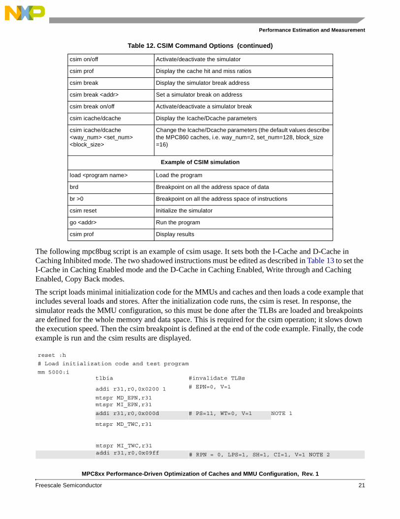
3.2 Cache Hit/Miss RatioThe cache hit ratio of an application is useful to determine the impact of the finite cache size of a certain processor over its performance. It can also be used in the optimization process to determine the expected performance improvement of a faster memory system or to check the effect of various performance improvement measures. Since the MPC8xx architecture does not include a mechanism to count the cache hits and misses, the cache hit ratio can be determined using a simulator (for example, SIMPPC from Software Development Systems Inc.) or a trace tool such as the one included in the mpc8bug debugger (the csim - cache simulator command)1.
Table 12 lists the csim command options; you can retrieve this information using the ‘help csim’ command under mpc8bug). The cache parameters (the number of ways, sets and the block size) are user-defined, so it is possible to simulate the effect of various cache sizes. For example, the hit ratio of a 16 Kbyte I-Cache /8 Kbyte D-Cache device can be determined and compared to that of the existing 4 Kbyte I-Cache/4 Kbyte D-Cache controller.
1. The CSIM command was introduced experimentally and was not extensively tested.
Table 12. CSIM Command Options
Command Description
csim reset Initiate the simulator
MPC8xx Performance-Driven Optimization of Caches and MMU Configuration, Rev. 1
Freescale Semiconductor 21
Performance Estimation and Measurement
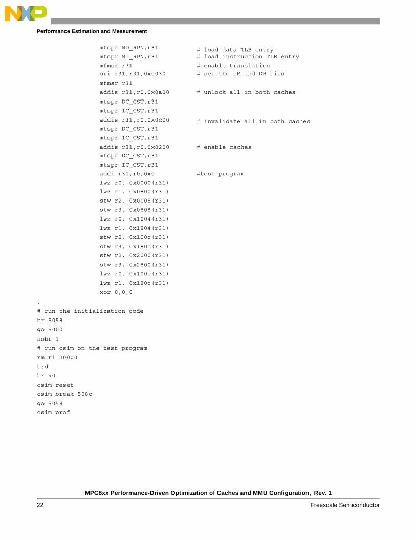
The following mpc8bug script is an example of csim usage. It sets both the I-Cache and D-Cache in Caching Inhibited mode. The two shadowed instructions must be edited as described in Table 13 to set the I-Cache in Caching Enabled mode and the D-Cache in Caching Enabled, Write through and Caching Enabled, Copy Back modes.
The script loads minimal initialization code for the MMUs and caches and then loads a code example that includes several loads and stores. After the initialization code runs, the csim is reset. In response, the simulator reads the MMU configuration, so this must be done after the TLBs are loaded and breakpoints are defined for the whole memory and data space. This is required for the csim operation; it slows down the execution speed. Then the csim breakpoint is defined at the end of the code example. Finally, the code example is run and the csim results are displayed.
csim on/off Activate/deactivate the simulator
csim prof Display the cache hit and miss ratios
csim break Display the simulator break address
csim break <addr> Set a simulator break on address
csim break on/off Activate/deactivate a simulator break
csim icache/dcache Display the Icache/Dcache parameters
csim icache/dcache <way_num> <set_num> <block_size>
Change the Icache/Dcache parameters (the default values describe the MPC860 caches, i.e. way_num=2, set_num=128, block_size =16)
Example of CSIM simulation
load <program name> Load the program
brd Breakpoint on all the address space of data
br >0 Breakpoint on all the address space of instructions
csim reset Initialize the simulator
go <addr> Run the program
csim prof Display results
reset :h
# Load initialization code and test program
mm 5000:itlbia #invalidate TLBs
addi r31,r0,0x0200 1 # EPN=0, V=1
mtspr MD_EPN,r31 mtspr MI_EPN,r31
addi r31,r0,0x000d # PS=11, WT=0, V=1 NOTE 1
mtspr MD_TWC,r31
mtspr MI_TWC,r31 addi r31,r0,0x09ff # RPN = 0, LPS=1, SH=1, CI=1, V=1 NOTE 2
Table 12. CSIM Command Options (continued)
MPC8xx Performance-Driven Optimization of Caches and MMU Configuration, Rev. 1
22 Freescale Semiconductor
Performance Estimation and Measurement
mtspr MD_RPN,r31 # load data TLB entry mtspr MI_RPN,r31 # load instruction TLB entry
mfmsr r31 # enable translation
ori r31,r31,0x0030 # set the IR and DR bits
mtmsr r31
addis r31,r0,0x0a00 # unlock all in both caches
mtspr DC_CST,r31
mtspr IC_CST,r31
addis r31,r0,0x0c00 # invalidate all in both caches mtspr DC_CST,r31
mtspr IC_CST,r31
addis r31,r0,0x0200 # enable caches
mtspr DC_CST,r31
mtspr IC_CST,r31
addi r31,r0,0x0 #test program
lwz r0, 0x0000(r31)
lwz r1, 0x0800(r31)
stw r2, 0x0008(r31)
stw r3, 0x0808(r31)
lwz r0, 0x1004(r31)
lwz r1, 0x1804(r31)
stw r2, 0x100c(r31)
stw r3, 0x180c(r31)
stw r2, 0x2000(r31)
stw r3, 0x2800(r31)
lwz r0, 0x100c(r31)
lwz r1, 0x180c(r31)
xor 0,0,0
.
# run the initialization code
br 5058
go 5000
nobr 1
# run csim on the test program
rm r1 20000
brd
br >0
csim reset
csim break 508c
go 5058
csim prof
MPC8xx Performance-Driven Optimization of Caches and MMU Configuration, Rev. 1
Freescale Semiconductor 23
Performance Estimation and Measurement
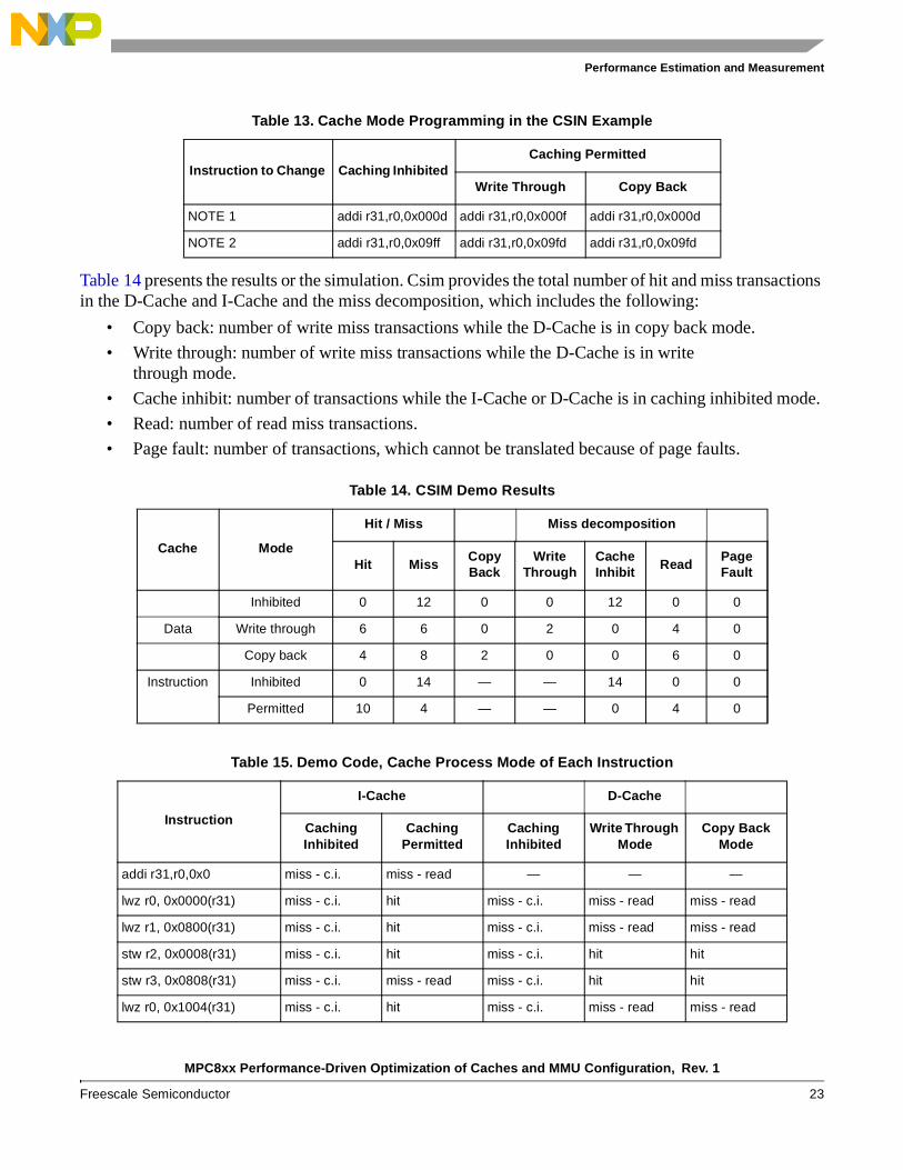
Table 14 presents the results or the simulation. Csim provides the total number of hit and miss transactions in the D-Cache and I-Cache and the miss decomposition, which includes the following:
• Copy back: number of write miss transactions while the D-Cache is in copy back mode.
• Write through: number of write miss transactions while the D-Cache is in writethrough mode.
• Cache inhibit: number of transactions while the I-Cache or D-Cache is in caching inhibited mode.
• Read: number of read miss transactions.
• Page fault: number of transactions, which cannot be translated because of page faults.
Table 13. Cache Mode Programming in the CSIN Example
Instruction to Change Caching Inhibited Caching Permitted
Write Through Copy Back
NOTE 1 addi r31,r0,0x000d addi r31,r0,0x000f addi r31,r0,0x000d
NOTE 2 addi r31,r0,0x09ff addi r31,r0,0x09fd addi r31,r0,0x09fd
Table 14. CSIM Demo Results
Cache Mode
Hit / Miss Miss decomposition
Hit Miss Copy Back
Write Through
Cache Inhibit Read
Page Fault
Inhibited 0 12 0 0 12 0 0
Data Write through 6 6 0 2 0 4 0
Copy back 4 8 2 0 0 6 0
Instruction Inhibited 0 14 — — 14 0 0
Permitted 10 4 — — 0 4 0
Table 15. Demo Code, Cache Process Mode of Each Instruction
Instruction
I-Cache D-Cache
Caching Inhibited
Caching Permitted
Caching Inhibited
Write Through Mode
Copy Back Mode
addi r31,r0,0x0 miss - c.i. miss - read — — —
lwz r0, 0x0000(r31) miss - c.i. hit miss - c.i. miss - read miss - read
lwz r1, 0x0800(r31) miss - c.i. hit miss - c.i. miss - read miss - read
stw r2, 0x0008(r31) miss - c.i. hit miss - c.i. hit hit
stw r3, 0x0808(r31) miss - c.i. miss - read miss - c.i. hit hit
lwz r0, 0x1004(r31) miss - c.i. hit miss - c.i. miss - read miss - read
MPC8xx Performance-Driven Optimization of Caches and MMU Configuration, Rev. 1
24 Freescale Semiconductor
Performance Estimation and Measurement
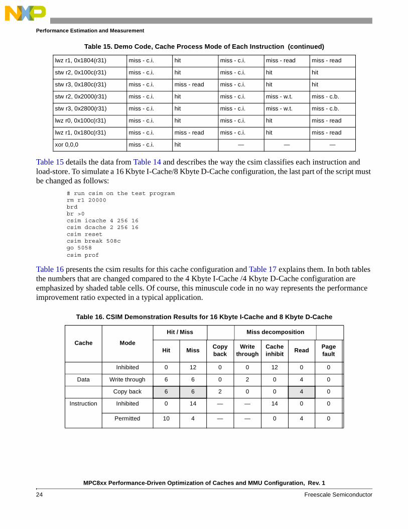
Table 15 details the data from Table 14 and describes the way the csim classifies each instruction and load-store. To simulate a 16 Kbyte I-Cache/8 Kbyte D-Cache configuration, the last part of the script must be changed as follows:
# run csim on the test programrm r1 20000brdbr >0csim icache 4 256 16csim dcache 2 256 16csim resetcsim break 508cgo 5058csim prof
Table 16 presents the csim results for this cache configuration and Table 17 explains them. In both tables the numbers that are changed compared to the 4 Kbyte I-Cache /4 Kbyte D-Cache configuration are emphasized by shaded table cells. Of course, this minuscule code in no way represents the performance improvement ratio expected in a typical application.
lwz r1, 0x1804(r31) miss - c.i. hit miss - c.i. miss - read miss - read
stw r2, 0x100c(r31) miss - c.i. hit miss - c.i. hit hit
stw r3, 0x180c(r31) miss - c.i. miss - read miss - c.i. hit hit
stw r2, 0x2000(r31) miss - c.i. hit miss - c.i. miss - w.t. miss - c.b.
stw r3, 0x2800(r31) miss - c.i. hit miss - c.i. miss - w.t. miss - c.b.
lwz r0, 0x100c(r31) miss - c.i. hit miss - c.i. hit miss - read
lwz r1, 0x180c(r31) miss - c.i. miss - read miss - c.i. hit miss - read
xor 0,0,0 miss - c.i. hit — — —
Table 16. CSIM Demonstration Results for 16 Kbyte I-Cache and 8 Kbyte D-Cache
Cache Mode
Hit / Miss Miss decomposition
Hit Miss Copy back
Write through
Cache inhibit
Read Page fault
Inhibited 0 12 0 0 12 0 0
Data Write through 6 6 0 2 0 4 0
Copy back 6 6 2 0 0 4 0
Instruction Inhibited 0 14 — — 14 0 0
Permitted 10 4 — — 0 4 0
Table 15. Demo Code, Cache Process Mode of Each Instruction (continued)
MPC8xx Performance-Driven Optimization of Caches and MMU Configuration, Rev. 1
Freescale Semiconductor 25
Performance Estimation and Measurement
3.3 Instructions Per ClockThe number of instructions executed per clock cycle (IPC) is an important indication of system performance. The IPC can be used as follows:
• To determine whether a system is correctly initialized and takes full advantage of the caches and MMUs. The MPC8xx includes a single-issue core, so the maximum theoretic IPC is 1. In a real application, the IPC is less than one because of the blockage, latency and synchronization requirements of the internal instruction execution. The IPC is also significantly affected by development support overhead and application-dependent factors such as memory access latency (cache hit ratio, cache mode - write through or copy back, guarded storage, number of wait states in the external memory accesses). An IPC of 0.7 or more indicates that the processor resources are efficiently used while an IPC less of 0.4 suggests significant deficiencies.
• To measure the effect of different optimization measures.
• To benchmark.
A simple performance meter to measure the IPC can be built using the MPC8xx internal resources. The performance meter performs the following tasks:
• Counts the instructions executed in a certain program segment.
• Counts the clock cycles to execute the same program segment.
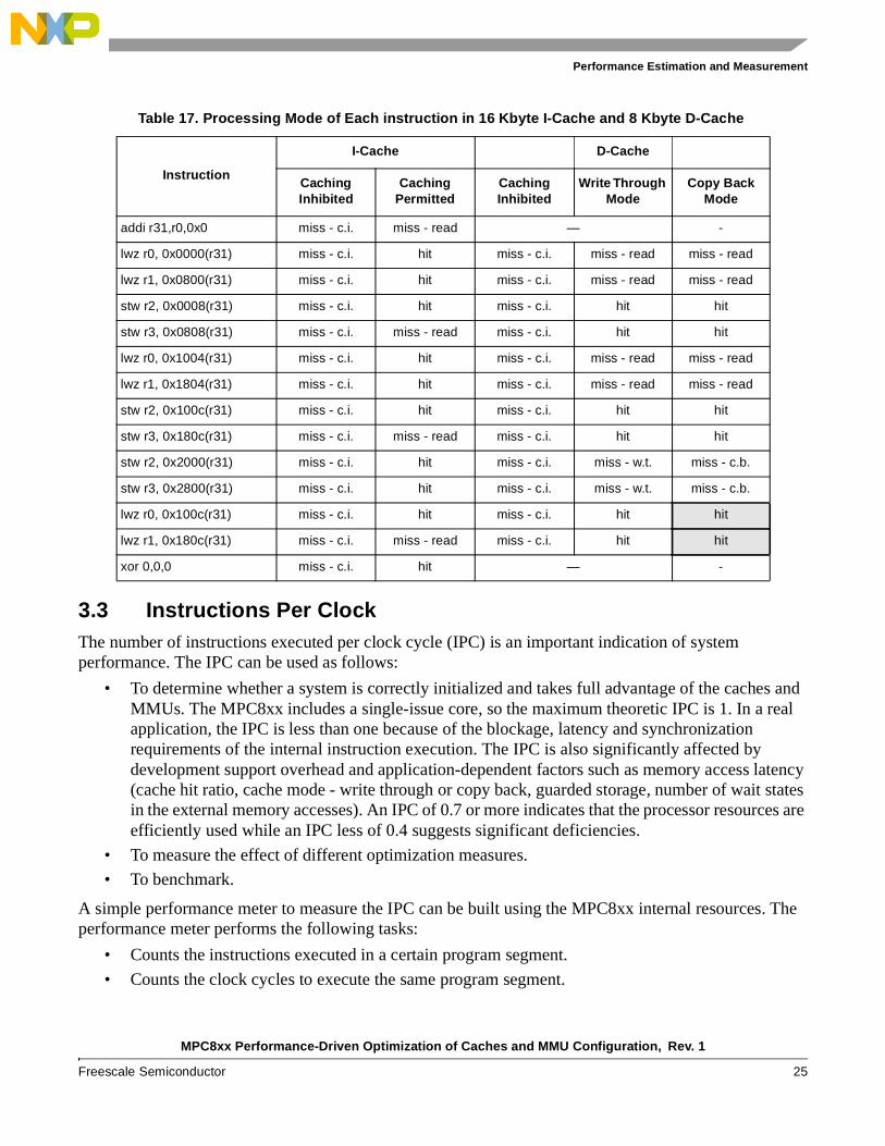
Table 17. Processing Mode of Each instruction in 16 Kbyte I-Cache and 8 Kbyte D-Cache
Instruction
I-Cache D-Cache
Caching Inhibited
Caching Permitted
Caching Inhibited
Write Through Mode
Copy Back Mode
addi r31,r0,0x0 miss - c.i. miss - read — -
lwz r0, 0x0000(r31) miss - c.i. hit miss - c.i. miss - read miss - read
lwz r1, 0x0800(r31) miss - c.i. hit miss - c.i. miss - read miss - read
stw r2, 0x0008(r31) miss - c.i. hit miss - c.i. hit hit
stw r3, 0x0808(r31) miss - c.i. miss - read miss - c.i. hit hit
lwz r0, 0x1004(r31) miss - c.i. hit miss - c.i. miss - read miss - read
lwz r1, 0x1804(r31) miss - c.i. hit miss - c.i. miss - read miss - read
stw r2, 0x100c(r31) miss - c.i. hit miss - c.i. hit hit
stw r3, 0x180c(r31) miss - c.i. miss - read miss - c.i. hit hit
stw r2, 0x2000(r31) miss - c.i. hit miss - c.i. miss - w.t. miss - c.b.
stw r3, 0x2800(r31) miss - c.i. hit miss - c.i. miss - w.t. miss - c.b.
lwz r0, 0x100c(r31) miss - c.i. hit miss - c.i. hit hit
lwz r1, 0x180c(r31) miss - c.i. miss - read miss - c.i. hit hit
xor 0,0,0 miss - c.i. hit — -
MPC8xx Performance-Driven Optimization of Caches and MMU Configuration, Rev. 1
26 Freescale Semiconductor
Performance Estimation and Measurement
The IPC can than be determined by dividing these two results. To count the instructions executed, the hardware watchpoint/breakpoint generation is used in the following procedure:
1. Program comparator A (CMPA) to generate a watchpoint for each instruction (with the address larger than 0).
2. Program counter A (COUNTA) to decrement at each watchpoint.
3. Reset the COUNTA at the beginning of the code segment where the IPC must be measured.
4. Read the COUNTA after the code segment executes.
COUNTA has 16 bits, so up to 65536 instruction can be counted without software assistance. To count the clock cycles, the decrementor (DEC) can be used (it decrements each 16 clock cycles).
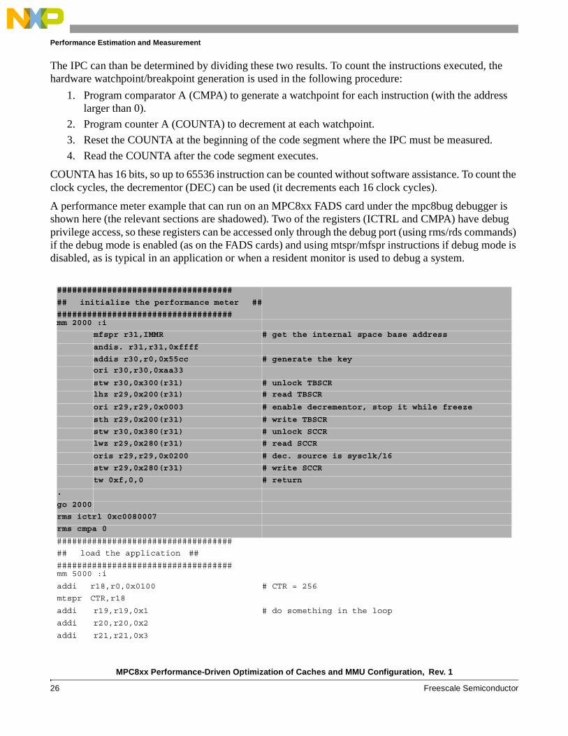
A performance meter example that can run on an MPC8xx FADS card under the mpc8bug debugger is shown here (the relevant sections are shadowed). Two of the registers (ICTRL and CMPA) have debug privilege access, so these registers can be accessed only through the debug port (using rms/rds commands) if the debug mode is enabled (as on the FADS cards) and using mtspr/mfspr instructions if debug mode is disabled, as is typical in an application or when a resident monitor is used to debug a system.
###################################
## initialize the performance meter ##
###################################mm 2000 :i
mfspr r31,IMMR # get the internal space base address
andis. r31,r31,0xffff
addis r30,r0,0x55cc # generate the key
ori r30,r30,0xaa33
stw r30,0x300(r31) # unlock TBSCR
lhz r29,0x200(r31) # read TBSCR
ori r29,r29,0x0003 # enable decrementor, stop it while freeze
sth r29,0x200(r31) # write TBSCR
stw r30,0x380(r31) # unlock SCCR
lwz r29,0x280(r31) # read SCCR
oris r29,r29,0x0200 # dec. source is sysclk/16
stw r29,0x280(r31) # write SCCR
tw 0xf,0,0 # return
.
go 2000
rms ictrl 0xc0080007
rms cmpa 0
###################################
## load the application ##
###################################mm 5000 :i
addi r18,r0,0x0100 # CTR = 256
mtspr CTR,r18
addi r19,r19,0x1 # do something in the loop
addi r20,r20,0x2
addi r21,r21,0x3
MPC8xx Performance-Driven Optimization of Caches and MMU Configuration, Rev. 1
Freescale Semiconductor 27
Performance Estimation and Measurement
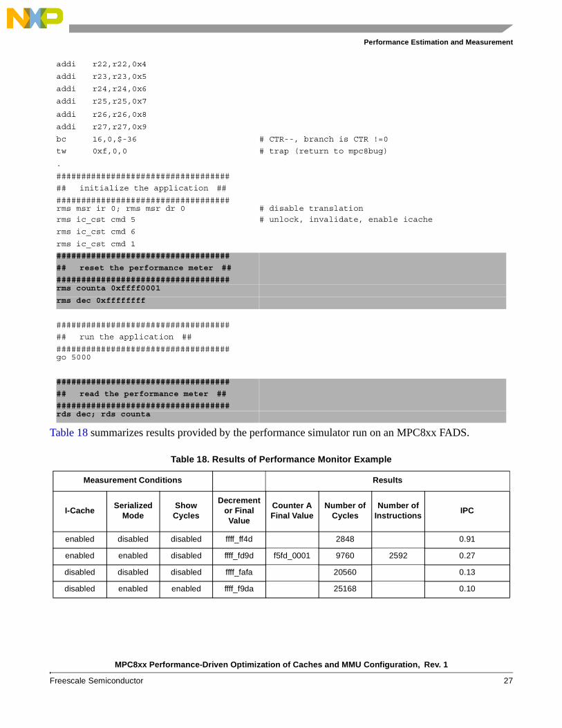
Table 18 summarizes results provided by the performance simulator run on an MPC8xx FADS.
addi r22,r22,0x4
addi r23,r23,0x5
addi r24,r24,0x6
addi r25,r25,0x7
addi r26,r26,0x8
addi r27,r27,0x9
bc 16,0,$-36 # CTR--, branch is CTR !=0
tw 0xf,0,0 # trap (return to mpc8bug)
.
###################################
## initialize the application ##
###################################rms msr ir 0; rms msr dr 0 # disable translation
rms ic_cst cmd 5 # unlock, invalidate, enable icache
rms ic_cst cmd 6
rms ic_cst cmd 1
###################################
## reset the performance meter ##
###################################rms counta 0xffff0001
rms dec 0xffffffff
###################################
## run the application ##
###################################go 5000
###################################
## read the performance meter ##
###################################rds dec; rds counta
Table 18. Results of Performance Monitor Example
Measurement Conditions Results
I-Cache Serialized
Mode Show Cycles
Decrementor Final Value
Counter A Final Value
Number of Cycles
Number of Instructions
IPC
enabled disabled disabled ffff_ff4d 2848 0.91
enabled enabled disabled ffff_fd9d f5fd_0001 9760 2592 0.27
disabled disabled disabled ffff_fafa 20560 0.13
disabled enabled enabled ffff_f9da 25168 0.10
Document Number: AN3066Rev. 101/2006
Freescale™ and the Freescale logo are trademarks of Freescale Semiconductor, Inc. All other product or service names are the property of their respective owners.
© Freescale Semiconductor, Inc., 2002, 2006.
Information in this document is provided solely to enable system and software
implementers to use Freescale Semiconductor products. There are no express or
implied copyright licenses granted hereunder to design or fabricate any integrated
circuits or integrated circuits based on the information in this document.
Freescale Semiconductor reserves the right to make changes without further notice to
any products herein. Freescale Semiconductor makes no warranty, representation or
guarantee regarding the suitability of its products for any particular purpose, nor does
Freescale Semiconductor assume any liability arising out of the application or use of
any product or circuit, and specifically disclaims any and all liability, including without
limitation consequential or incidental damages. “Typical” parameters which may be
provided in Freescale Semiconductor data sheets and/or specifications can and do
vary in different applications and actual performance may vary over time. All operating
parameters, including “Typicals” must be validated for each customer application by
customer’s technical experts. Freescale Semiconductor does not convey any license
under its patent rights nor the rights of others. Freescale Semiconductor products are
not designed, intended, or authorized for use as components in systems intended for
surgical implant into the body, or other applications intended to support or sustain life,
or for any other application in which the failure of the Freescale Semiconductor product
could create a situation where personal injury or death may occur. Should Buyer
purchase or use Freescale Semiconductor products for any such unintended or
unauthorized application, Buyer shall indemnify and hold Freescale Semiconductor
and its officers, employees, subsidiaries, affiliates, and distributors harmless against all
claims, costs, damages, and expenses, and reasonable attorney fees arising out of,
directly or indirectly, any claim of personal injury or death associated with such
unintended or unauthorized use, even if such claim alleges that Freescale
Semiconductor was negligent regarding the design or manufacture of the part.
How to Reach Us:
Home Page: www.freescale.com
email: [email protected]
USA/Europe or Locations Not Listed: Freescale Semiconductor Technical Information Center, CH3701300 N. Alma School Road Chandler, Arizona 85224 [email protected]
Europe, Middle East, and Africa:Freescale Halbleiter Deutschland GmbHTechnical Information CenterSchatzbogen 781829 Muenchen, Germany+44 1296 380 456 (English) +46 8 52200080 (English)+49 89 92103 559 (German)+33 1 69 35 48 48 (French) [email protected]
Japan: Freescale Semiconductor Japan Ltd. HeadquartersARCO Tower 15F1-8-1, Shimo-Meguro, Meguro-ku Tokyo 153-0064, Japan 0120 191014+81 3 5437 [email protected]
Asia/Pacific: Freescale Semiconductor Hong Kong Ltd. Technical Information Center2 Dai King Street Tai Po Industrial Estate, Tai Po, N.T., Hong Kong +800 2666 [email protected]
For Literature Requests Only:Freescale Semiconductor
Literature Distribution Center P.O. Box 5405Denver, Colorado 80217 1-800-441-2447303-675-2140Fax: 303-675-2150LDCForFreescaleSemiconductor
@hibbertgroup.com