Embed Size (px)
Citation preview

Freescale SemiconductorApplication Note
© Freescale Semiconductor, Inc., 2010. All rights reserved.
This document provides recommendations for new designs based on the MPC8548E PowerQUICC™ III family of integrated host communications processors (collectively referred to throughout this document as MPC8548E):
• MPC8548E
• MPC8548
• MPC8547E
• MPC8545E
• MPC8545
• MPC8543E
• MPC8543
This document may also be useful in debugging newly designed systems by highlighting those aspects of a design that merit special attention during initial system startup.
For updates to this document, refer to the website listed on the back cover of this document.
Document Number: AN3640Rev. 3, 08/2010
Contents1. Introduction . . . . . . . . . . . . . . . . . . . . . . . . . . . . . . . . . 22. Power . . . . . . . . . . . . . . . . . . . . . . . . . . . . . . . . . . . . . 43. Power-On Reset and Reset Configurations . . . . . . . . 84. Device Pins . . . . . . . . . . . . . . . . . . . . . . . . . . . . . . . . 126. DDR Interface . . . . . . . . . . . . . . . . . . . . . . . . . . . . . . 147. Debug and Test Interface . . . . . . . . . . . . . . . . . . . . . 158. DMA Interface . . . . . . . . . . . . . . . . . . . . . . . . . . . . . 169. DUART Interface . . . . . . . . . . . . . . . . . . . . . . . . . . . 17
10. Ethernet Management Interface . . . . . . . . . . . . . . . . 1711. eTSEC Interface . . . . . . . . . . . . . . . . . . . . . . . . . . . . 1812. I2C Interface . . . . . . . . . . . . . . . . . . . . . . . . . . . . . . . 1913. JTAG Interface . . . . . . . . . . . . . . . . . . . . . . . . . . . . . 1914. Local Bus Interface . . . . . . . . . . . . . . . . . . . . . . . . . . 2315. PCI Interface . . . . . . . . . . . . . . . . . . . . . . . . . . . . . . . 2516. PIC Interface . . . . . . . . . . . . . . . . . . . . . . . . . . . . . . . 2717. SerDes Interface . . . . . . . . . . . . . . . . . . . . . . . . . . . . 2718. System Control . . . . . . . . . . . . . . . . . . . . . . . . . . . . . 2819. Reserved Pins . . . . . . . . . . . . . . . . . . . . . . . . . . . . . . 2820. Power and Ground Signals . . . . . . . . . . . . . . . . . . . . 2921. Revision History . . . . . . . . . . . . . . . . . . . . . . . . . . . . 29
MPC8548E PowerQUICC III Family Bring-Up Guide

MPC8548E PowerQUICC III Family Bring-Up Guide, Rev. 3
2 Freescale Semiconductor
Introduction
1 IntroductionThis section outlines recommendations to simplify the first phase of design. Before designing a system with an MPC8548E device, it is recommended that the designer be familiar with the available documentation, software, models, and tools.
1.1 ReferencesSome references listed here may be available only under a non-disclosure agreement (NDA). Contact your local field applications engineer or sales representative to obtain a copy.
• Collateral
— MPC8548E PowerQUICC III™ Integrated Host Processor Family Reference Manual (MPC8548ERM)
— Errata to MPC8548E PowerQUICC™ III Integrated Host Processor Family Reference Manual (MPC8548ERMAD)
— Device Errata for the MPC8548E PowerQUICC™ III (MPC8548ECE)
— MPC8548E PowerQUICC III™ Integrated Processor Hardware Specifications (MPC8548EEC)
• Tools
— Boot sequencer generator tool
— UPM Programming tool
• Models
— IBIS
— BSDL
1.2 Device ErrataThe device errata document describes the latest fixes and work arounds for the MPC8548E. The errata document should be thoroughly researched prior to starting a design with the respective MPC8548E device.
1.3 Boot Sequencer ToolThe MPC8548E features the boot sequencer to allow configuration of any memory-mapped register before the completion of power-on reset (POR). The register data to be changed is stored in an I2C EEPROM. The MPC8548E requires a particular data format for register changes as outlined in the MPC8548ERM. The boot sequencer tool is a C-code file. When compiled and given a sample data file, it generates the appropriate raw data format as outlined in the MPC8548ERM (that is, an s-record file that can be used to program the EEPROM).

MPC8548E PowerQUICC III Family Bring-Up Guide, Rev. 3
Freescale Semiconductor 3
Introduction
1.4 UPM Programming ToolThe UPM programming tool features a GUI for a user-friendly programming interface. It allows programming of all three of the MPC8548E’s UPM machines. The GUI consists of a wave editor, a table editor, and a report generator. The user can edit the waveform directly or the RAM array directly. At the end of programming, the report generator prints out the UPM RAM array that can be used in a C-program.
1.5 Available TrainingOur third-party partners are part of an extensive Design Alliance Program. The current training partners can be found on our website under Design Alliance Program.
Training material from past Smart Network Developer’s Forums and Freescale Technology Forums are also available. These trainings modules are a valuable resource in understanding the MPC8548E. This material is also available at our website listed on the back cover of this document.
1.6 Product RevisionsTable 1 lists the processor version register (PVR) and system version register (SVR) values for the various MPC8548E derivatives of silicon.
Table 1. MPC8548E PowerQUICC III Product Revisions
Silicon Version Device Number Core Revision Processor Version Register (PVR) Value
System Version Register (SVR) Value
Ver. 2.0 MPC8548 Rev. 2.0 0x8021_0020 0x8031_0020
MPC8548E 0x8039_0020
MPC8547E 0x8039_0120
MPC8545 0x8031_0220
MPC8545E 0x8039_0220
MPC8543 0x8032_0020
MPC8543E 0x803A_0020
Ver. 2.1 MPC8548 Rev. 2.2 0x8021_0022 0x8031_0021
MPC8548E 0x8039_0021
MPC8547E 0x8039_0121
MPC8545 0x8031_0221
MPC8545E 0x8039_0221
MPC8543 0x8032_0021
MPC8543E 0x803A_0021
MPC8548E PowerQUICC III Family Bring-Up Guide, Rev. 3
4 Freescale Semiconductor
Power
2 PowerThis section provides design considerations for the MPC8548E power supplies, as well as power sequencing. For information on AC and DC electrical specifications and thermal characteristics for the MPC8548E, refer to the MPC8548E Hardware Specification (MPC8548EEC).
2.1 Power SuppliesThe MPC8548E has a core voltage VDD and SerDes voltages SVDD and XVDD, which operate at a lower voltage than the I/O voltages BVDD, GVDD, LVDD, OVDD, and TVDD. It is recommended that the core voltage VDD of MPC8548E be supplied through a variable switching supply or regulator to allow for future compatibility with possible core voltage changes on future silicon revisions. The core voltage, 1.1 V (±5%), is supplied across VDD and GND.
The I/O blocks of the MPC8548E are supplied with the following:
• 2.5 V (±5%) or 3.3 V (±5%) across BVDD and GND
• 1.8 V (±5%) or 2.5 V (±5%) across GVDD and GND
• 2.5 V (±5%) or 3.3 V (±5%) across LVDD and GND
• 3.3 V (±5%) across OVDD and GND
• 1.1 V (±5%) across SVDD and GND
• 2.5 V (±5%) or 3.3 V (±5%) across TVDD and GND
• 1.1 V (±5%) across XVDD and GND
Typically, these are supplied by simple linear regulators. This increases the complexity of the system because multiple voltage supplies and PCB power planes are required for the design.
Both LVDD and TVDD are used to supply the eTSEC interfaces on the device; LVDD manages eTSEC1 and eTSEC2, and TVDD manages eTSEC3 and eTSEC4. For the respective eTSEC, LVDD/TVDD must be the following:
• 3.3 V for GMII, MII, RMII, or TBI modes of operation
• 2.5 V for GMII, RGMII, RTBI, or FIFO modes of operation
NOTEAs a result, 3.3 V and 2.5 V modes cannot be paired on eTSECs powered by the same I/O supply on the MPC8548E.
2.2 Power ConsumptionOperating-mode power dissipation numbers (TYPICAL) are provided in the MPC8548E Hardware Specification (MPC8548EEC). Two TYPICAL numbers are provided, one at 65 °C and one at 105 °C, to assist in the thermal design for the device. If the targeted junction temperature (TJ) of the MPC8548E in the system is not one of these two temperatures, a linear extrapolation of these two TYPICAL dissipation values can be used to estimate the power dissipation at the targeted junction temperature.
The MAXIMUM number, provided at 105 °C, is intended to assist in the power supply design selection.
MPC8548E PowerQUICC III Family Bring-Up Guide, Rev. 3
Freescale Semiconductor 5
Power
A low-power SLEEP mode dissipation (at 65 °C) is also provided for applications concerned about minimizing power consumption when the MPC8548E is not active.
NOTEThe SLEEP, TYPICAL, and MAXIMUM power numbers are based on the power dissipation on the 1.1 V nominal VDD supply only. Typical power dissipation estimates on the peripheral supplies (BVDD, GVDD, LVDD, OVDD, TVDD, and XVDD) are provided in the MPC8548EEC document.
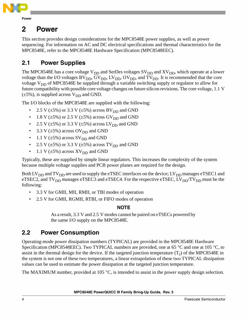
2.3 I/O Power DissipationI/O usage varies from design to design. Table 2 provides power dissipation estimates for the I/O supplies.
Table 2. Estimated I/O Power Dissipation
Interface Parameters1.1 V
(XVDD)1.8 V
(GVDD)2.5 V
(B/G/LVDD)3.3 V
(B/L/OVDD) Comments
DDR 266 MHz data — 0.31 W 0.59W — —
333 MHz data — 0.38 W 0.73W —
400 MHz data 0.46 W
533 MHz data — 0.60 W — —
PCI Express x8, 2.5 G-baud 0.71 W — — — —
Serial RapidIO x4, 2.5 G-baud 0.49 W — — — —
PCI Express 64-bit, 133 MHz — — — 0.25 W —
PCI 64-bit, 66 MHz — — — 0.14 W Power per PCI port
64-bit, 66 MHz — — — 0.08 W
32-bit, 66 MHz — — — 0.07 W
32-bit, 33 MHz — — — 0.04 W
Local bus 32-bit, 133 MHz — — 0.14 W 0.24 W —
32-bit, 66 MHz — — 0.07 W 0.13 W
32-bit, 33 MHz — — 0.04 W 0.07 W
eTSEC (10/100/1000
Ethernet)
MII — — — 0.01 W Power per eTSEC used
GMII — — — 0.07 W
TBI — — — 0.07 W
RGMII — — 0.04 W —
RTBI — — 0.04 W —
eTSEC (packet FIFO)
8-bit, 200 MHz — — 0.11 W — Power per FIFO interface used
8-bit, 155 MHz — — 0.08 W —
MPC8548E PowerQUICC III Family Bring-Up Guide, Rev. 3
6 Freescale Semiconductor
Power
2.4 Power SequencingThe device requires its power rails to be applied in a specific sequence to ensure proper device operation. These requirements per the MPC8548EEC document are as follows for power-up:
1. VDD, AVDD_n, BVDD, LVDD, OVDD, SVDD, TVDD, XVDD
2. GVDD
All supplies must be at their stable values within 50 ms.
The purpose of the sequence is to guarantee the state of the DDR signals at reset. In order to guarantee MCKE low during power-up (as should be attempted per the JEDEC JESD79-2C specification), the above sequencing for GVDD is required. If there is no concern about any of the DDR signals being in an indeterminate state during power-up, then the sequencing of GVDD is not required.
From a system standpoint, if any of the I/O power supplies ramp prior to the VDD core supply, the I/Os associated with that I/O supply may drive a logic one or zero during power-up, and extra current may be drawn by the device.
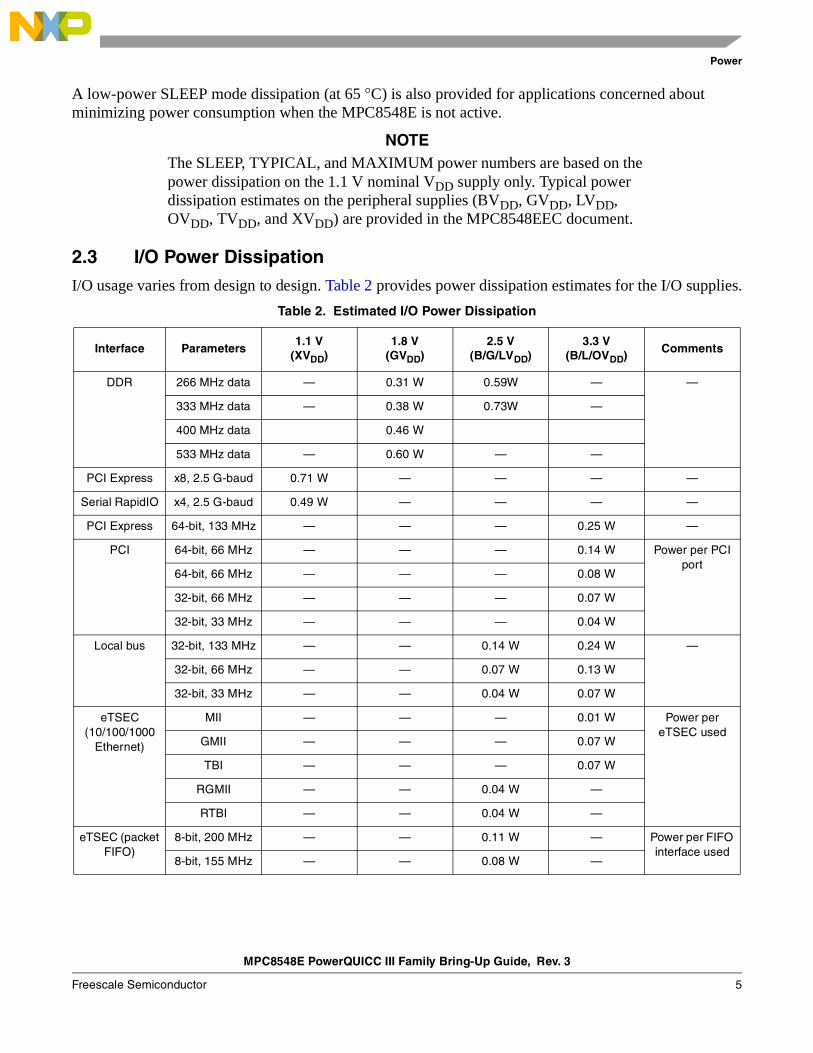
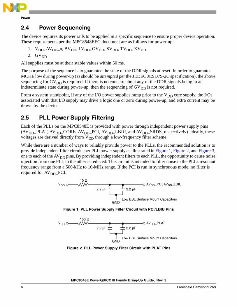
2.5 PLL Power Supply FilteringEach of the PLLs on the MPC8548E is provided with power through independent power supply pins (AVDD_PLAT, AVDD_CORE, AVDD_PCI, AVDD_LBIU, and AVDD_SRDS, respectively). Ideally, these voltages are derived directly from VDD through a low-frequency filter scheme.
While there are a number of ways to reliably provide power to the PLLs, the recommended solution is to provide independent filter circuits per PLL power supply as illustrated in Figure 1, Figure 2, and Figure 3, one to each of the AVDD pins. By providing independent filters to each PLL, the opportunity to cause noise injection from one PLL to the other is reduced. This circuit is intended to filter noise in the PLLs resonant frequency range from a 500-kHz to 10-MHz range. If the PCI is run in synchronous mode, no filter is required for AVDD_PCI.
Figure 1. PLL Power Supply Filter Circuit with PCI/LBIU Pins
Figure 2. PLL Power Supply Filter Circuit with PLAT Pins
VDD AVDD_PCI/AVDD_LBIU
2.2 µF 2.2 µF
GNDLow ESL Surface Mount Capacitors
10 Ω
VDD AVDD_PLAT
2.2 µF 2.2 µF
GNDLow ESL Surface Mount Capacitors
150 Ω
MPC8548E PowerQUICC III Family Bring-Up Guide, Rev. 3
Freescale Semiconductor 7
Power
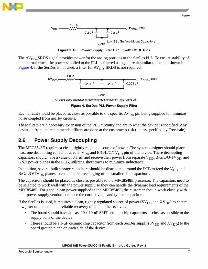
Figure 3. PLL Power Supply Filter Circuit with CORE Pins
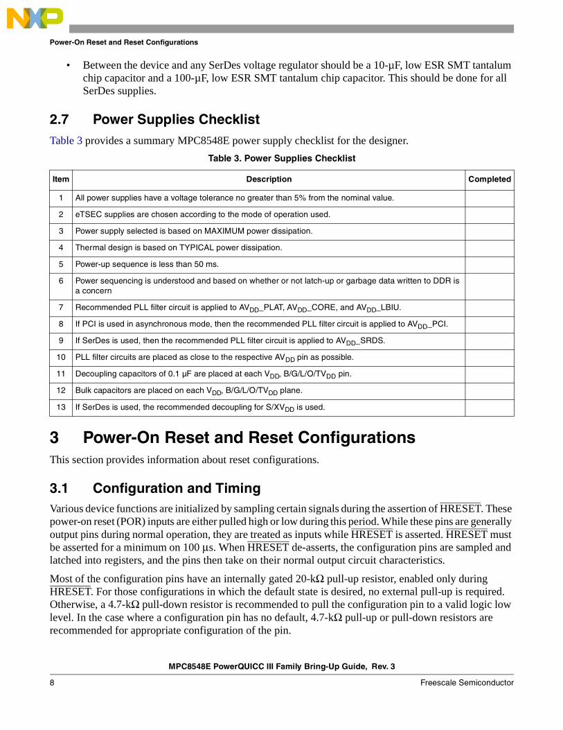
The AVDD_SRDS signal provides power for the analog portions of the SerDes PLL. To ensure stability of the internal clock, the power supplied to the PLL is filtered using a circuit similar to the one shown in Figure 4. If the SerDes is not used, a filter for AVDD_SRDS is not required.
Figure 4. SerDes PLL Power Supply Filter
Each circuit should be placed as close as possible to the specific AVDD pin being supplied to minimize noise coupled from nearby circuits.
These filters are a necessary extension of the PLL circuitry and are to what the device is specified. Any deviation from the recommended filters are done at the customer’s risk (unless specified by Freescale).
2.6 Power Supply DecouplingThe MPC8548E requires a clean, tightly regulated source of power. The system designer should place at least one decoupling capacitor at each VDD and B/G/L/O/TVDD pin of the device. These decoupling capacitors should have a value of 0.1 µF and receive their power from separate VDD, B/G/L/O/TVDD, and GND power planes in the PCB, utilizing short traces to minimize inductance.
In addition, several bulk storage capacitors should be distributed around the PCB to feed the VDD and B/G/L/O/TVDD planes to enable quick recharging of the smaller chip capacitors.
The capacitors should be placed as close as possible to the MPC8548E processor. The capacitors need to be selected to work well with the power supply so they can handle the dynamic load requirements of the MPC8548E. For good, clean power supplied to the MPC8548E, the customer should work closely with their power-supply vendor to choose the correct value and type of capacitors.
If the SerDes is used, it requires a clean, tightly regulated source of power (SVDD and XVDD) to ensure low jitter on transmit and reliable recovery of data in the receiver:
• The board should have at least 10 x 10-nF SMT ceramic chip capacitors as close as possible to the supply balls of the device.
• There should be a 1-µF ceramic chip capacitor from each SerDes supply (SVDD and XVDD) to the board ground plane on each side of the device.
VDD AVDD_CORE
2.2 µF 2.2 µF
GNDLow ESL Surface Mount Capacitors
180 Ω
2.2 µF 1 0.003 µF
GND
1.0 ΩAVDD_SRDS
1. An 0805 sized capacitor is recommended for system initial bring-up.
SVDD
2.2 µF 1
MPC8548E PowerQUICC III Family Bring-Up Guide, Rev. 3
8 Freescale Semiconductor
Power-On Reset and Reset Configurations
• Between the device and any SerDes voltage regulator should be a 10-µF, low ESR SMT tantalum chip capacitor and a 100-µF, low ESR SMT tantalum chip capacitor. This should be done for all SerDes supplies.
2.7 Power Supplies ChecklistTable 3 provides a summary MPC8548E power supply checklist for the designer.
3 Power-On Reset and Reset ConfigurationsThis section provides information about reset configurations.
3.1 Configuration and TimingVarious device functions are initialized by sampling certain signals during the assertion of HRESET. These power-on reset (POR) inputs are either pulled high or low during this period. While these pins are generally output pins during normal operation, they are treated as inputs while HRESET is asserted. HRESET must be asserted for a minimum on 100 μs. When HRESET de-asserts, the configuration pins are sampled and latched into registers, and the pins then take on their normal output circuit characteristics.
Most of the configuration pins have an internally gated 20-kΩ pull-up resistor, enabled only during HRESET. For those configurations in which the default state is desired, no external pull-up is required. Otherwise, a 4.7-kΩ pull-down resistor is recommended to pull the configuration pin to a valid logic low level. In the case where a configuration pin has no default, 4.7-kΩ pull-up or pull-down resistors are recommended for appropriate configuration of the pin.
Table 3. Power Supplies Checklist
Item Description Completed
1 All power supplies have a voltage tolerance no greater than 5% from the nominal value.
2 eTSEC supplies are chosen according to the mode of operation used.
3 Power supply selected is based on MAXIMUM power dissipation.
4 Thermal design is based on TYPICAL power dissipation.
5 Power-up sequence is less than 50 ms.
6 Power sequencing is understood and based on whether or not latch-up or garbage data written to DDR is a concern
7 Recommended PLL filter circuit is applied to AVDD_PLAT, AVDD_CORE, and AVDD_LBIU.
8 If PCI is used in asynchronous mode, then the recommended PLL filter circuit is applied to AVDD_PCI.
9 If SerDes is used, then the recommended PLL filter circuit is applied to AVDD_SRDS.
10 PLL filter circuits are placed as close to the respective AVDD pin as possible.
11 Decoupling capacitors of 0.1 µF are placed at each VDD, B/G/L/O/TVDD pin.
12 Bulk capacitors are placed on each VDD, B/G/L/O/TVDD plane.
13 If SerDes is used, the recommended decoupling for S/XVDD is used.
MPC8548E PowerQUICC III Family Bring-Up Guide, Rev. 3
Freescale Semiconductor 9
Power-On Reset and Reset Configurations
An alternative to using pull-up and pull-down resistors to configure the POR pins is to use a PLD or similar device which drives the configuration signals to the MPC8548E when HRESET is asserted. The PLD must begin to drive these signals at least 4 SYSCLK cycles prior to the de-assertion of HRESET (PLL configuration inputs must meet a 100-μs set-up time to HRESET), hold their values for at least 2 SYSCLK cycles after the de-assertion of HRESET, and then release the pins to high impedance afterward for normal device operation.
3.2 Configuration SettingsTable 4 summarizes the customer-configurable device settings for the MPC8548E. Refer to the MPC8548ERM for a more detailed description of each configuration option.
Table 4. User Configuration Options
Configuration Type Functional Pins Comments
MPC8548E Derivative DMA_DACK[0:1] There is no default value for this family device selection; these signals must be pulled to the desired value. Note: A family derivative with features not supported is not guaranteed to function if reconfigured as a fully featured derivative. For more information, see Table 5.
CCB Clock PLL Ratio LA[28:31] There is no default value for this PLL ratio; these signals must be pulled to the desired value
e500 Core PLL Ratio LBCTL, LALE, LGPL2 There is no default value for this PLL ratio; these signals must be pulled to the desired value
Boot ROM Location TSEC1_TXD[6:4] Default: Local Bus GPCM (32-bit ROM)
Host/Agent LWE[1:3] Default: MPC8548E acts as the host processor/root complex
I/O Port Selection TSEC1_TXD[3:1] Default: PCI Express x8 (2.5 Gbps); 100-MHz reference clock
CPU Boot LA27 Default: e500 core is allowed to boot without waiting for configuration by an external master.
Boot Sequencer LGPL3, LGPL5 Default: Boot sequencer is disabled.
DDR DRAM Type TSEC2_TXD1, TSEC2_TX_ER
Default: DDR controller is configured for DDR2
eTSEC1/2 Width EC_MDC Default: eTSEC1 and eTSEC2 Ethernet interfaces operate in their standard width TBI, GMII, MII. Or, if eTSEC1 is in FIFO mode, it operates as a 16-bit FIFO. eTSEC2 FIFO width is 8 bits regardless of this configuration setting.
eTSEC3/4 Width TSEC3_TXD2 Default: eTSEC3 Ethernet interface operates in standard TBI, GMII, MII, or 8-bit FIFO mode. eTSEC 4 is unavailable.
eTSEC1 Protocol TSEC1_TXD0, TSEC1_TXD7
Default: The eTSEC1 controller operates using the TBI protocol (or RTBI if configured in reduced mode).
eTSEC2 Protocol TSEC2_TXD0, TSEC2_TXD7
Default: The eTSEC2 controller operates using the TBI protocol (or RTBI if configured in reduced mode).
eTSEC3 Protocol TSEC3_TXD0, TSEC3_TXD1
Default: The eTSEC3 controller operates using the TBI protocol (or RTBI if configured in reduced mode).
MPC8548E PowerQUICC III Family Bring-Up Guide, Rev. 3
10 Freescale Semiconductor
Power-On Reset and Reset Configurations
Table 5 shows the derivatives of the MPC8548E.
eTSEC4 Protocol TSEC4_TXD0, TSEC4_TXD1
Default: The eTSEC4 controller operates using the RTBI protocol.
RapidIO® Device ID TSEC2_TXD[2:4] Default: Device ID[5:7] default to 1s.
RapidIO System Size LGPL0 Default: Small system size (up to 256 devices).
PCI1 Clock Select PCI2_GNT3 Default: Synchronous mode. SYSCLK is used as the clock for the PCI1/PCI Express interface.
PCI2 Clock Select PCI2_GNT4 Default: Synchronous mode. SYSCLK is used as the clock for the PCI2 interface.
PCI1 Speed Configuration
LWE0 Default: PCI frequency above 33 MHz or PCI Express frequency above 66 MHz.
PCI2 Speed Configuration
LGPL1 Default: PCI frequency above 33 MHz.
PCI Bus Width PCI1_REQ64 Default: The PCI1/PCI Express interface operates as a 32-bit interface.
PCI1 I/O Impedance PCI1_GNT1 Default: 42-Ω I/O drivers are used on the PCI1/PCI Express interface.
PCI2 I/O Impedance PCI2_GNT1 Default: 42-Ω I/O drivers are used on the PCI2 interface.
PCI1/PCI Express Arbiter PCI1_GNT2 Default: The on-chip PCI1/PCI Express arbiter is enabled.
PCI2 Arbiter PCI2_GNT2 Default: The on-chip PCI2 arbiter is enabled.
PCI Debug Configuration PCI1_GNT3 Default: PCI operates in normal mode.
PCI Express Configuration
PCI1_GNT4 Default: Interface operates in PCI mode.
Memory Debug MSRCID0 Default: Debug information from the DDR SDRAM controller is driven on the MSRCID and MDVAL signals.
DDR Debug MSRCID1 Default: Debug information is not driven on ECC pins. ECC pins function in their normal mode.
SerDes Enable TSEC4_TXD2 Default: SerDes interface is enabled.
General Purpose POR Configuration
LAD[0:31] There is no default value for this general purpose POR.
Table 5. MPC8548E Derivatives
Part Number SVR DMA_DACK_B[0:1] Test_Sel
MPC8548E with Security 803_9_00_20 ‘b11 1
MPC8548 without Security 803_1_00_20 ‘b11 1
MPC8547 (always with Security) 803_9_01_20 ‘b01 1
MP8545E with Security 803_9_02_20 ‘b10 1
MPC8545 without Security 803_1_02_20 ‘b10 1
Table 4. User Configuration Options (continued)
Configuration Type Functional Pins Comments
MPC8548E PowerQUICC III Family Bring-Up Guide, Rev. 3
Freescale Semiconductor 11
Power-On Reset and Reset Configurations
3.3 Internal Test ModesSeveral pins double as test mode enables. These test modes are for internal use only. If enabled during reset, they may result in the MPC8548E not coming out of reset. Table 6 lists these pins and how they should be addressed during the reset sequence.
3.4 Reset ChecklistTable 7 provides a summary MPC8548E POR and reset checklist for the designer.
MPC8543E with Security 803_A_00_20 ‘b11 0
MPC8543 without Security 803_2_00_20 ‘b11 0
Table 6. Internal Test Mode Pins
Pin Group Pins Guideline for Reset
Debug TRIG_OUT/READY Since these pins have an internal pull-up enabled only at reset, they may be left floating if unconnected. Otherwise, they may need to be driven high (that is, by a PLD), if the device to which they are connected does not release these pins to high impedance during reset.
MSRCID2
MSRCID3
MSRCID4
Design For Test LSSD_MODE These pins must be pulled to OVDD via a 100 Ω–1 kΩ resistor.
L1_TSTCLK —
L2_TSTCLK
TEST_SEL These pins must be pulled up or down at time of reset according to Table 5.
eTSEC TSEC2_TXD5 Since these pins have an internal pull-up enabled only at reset, they may be left floating if unconnected. Otherwise, they may need to be driven high (that is, by a PLD), if the device to which they are connected does not release these pins to high impedance during reset.
TSEC2_TXD6
TSEC3_TXD3
TSEC3_TXD7/TSEC4_TXD3
Power Management ASLEEP
System Control HRESET_REQ
Table 7. Checklist for POR and Reset Configurations
Item Description Completed
1 HRESET is asserted for a minimum of 100 μs.
2 DMA_DACK[0:1] are configured to select the appropriate MPC8548E family derivative.
Table 5. MPC8548E Derivatives (continued)
Part Number SVR DMA_DACK_B[0:1] Test_Sel
MPC8548E PowerQUICC III Family Bring-Up Guide, Rev. 3
12 Freescale Semiconductor
Device Pins
4 Device PinsThis section provides the recommended test points and a device pin map.
4.1 Recommended Test PointsFor easier debug, it is recommended that the test points on the board include the following pins:
• CLK_OUT (helps verify the CCB clock)
• TRIG_OUT (helps verify the end of the reset sequence)
• ASLEEP (helps verify the end of the reset sequence)
• SENSEVDD (helps verify power plane VDD)
• SENSEVSS (helps verify ground plane VSS)
• HRESET_REQ (helps verify proper boot sequencer functions and reset requests)
3 Configuration pins are either appropriately tied-off with a 4.7-kΩ resistor, or driven by an external device (meeting their required setup and hold times).
4 PLL configurations are defined and meet the required set-up and hold times.
5 Internal test mode pins are guaranteed not to be low during reset.
Table 7. Checklist for POR and Reset Configurations (continued)
Item Description Completed
MPC8548E PowerQUICC III Family Bring-Up Guide, Rev. 3
Freescale Semiconductor 13
Device Pins
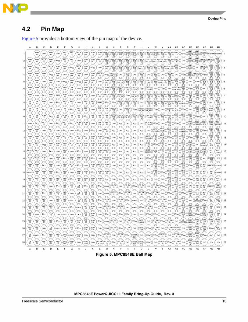
4.2 Pin MapFigure 5 provides a bottom view of the pin map of the device.
Figure 5. MPC8548E Ball Map
19
20
21
22
23
24
25
26
27
28
19
20
21
22
23
24
25
26
27
28
A UTRPNMLKJHGFEDCB V
1
2
3
4
5
6
7
8
9
10
11
12
13
14
15
16
17
18
1
2
3
4
5
6
7
8
9
10
11
12
13
14
15
16
17
18
W Y AA AB AC AD AE AF AG AH
THERM1THERM0MSRCID[3]
DMA_DACK
[1]
DMA_DDONE
[1]
MDQ[41] GND MDQ
[42] GND MCK[5]
MCK[2]
MDQS[6]
MDQ[56]
MDM[7]
MDQ[62]
TSEC2_RXD[1]
TSEC2_RXD[5]
TSEC2_COL
TSEC2_RX_ER
TSEC1_RX_ER
TSEC1_RXD[6]
TSEC1_RXD[2]
TSEC3_RX_DV
TSEC3_RXD[3]
TSEC4_RXD[3]
TRIG_OUT
MSRCID[4]
DMA_DREQ
[1]
DMA_DDONE
[0]
MDQ[45]
MDQ[46]
GVDDMCK[5]
MCK[2]
MDQ[61]
MDQ[57]
MDQS[7]
TSEC2_RXD[2]
TSEC2_RXD[4]
TSEC1_RXD[4]
TSEC3_RX_CLK
TSEC4_RXD[1]
TRIG_IN
MSRCID[2]
DMA_DACK
[0]GND MDQS
[5]MDQ[48]
MDQS[6]
MDQ[60]
TSEC2_RXD[0]
TSEC1_RXD[3]
TSEC4_RXD[2]
DMA_DREQ
[0]
MDQ[39]
MDQ[49]
MDM[6]
MDQ[55]
MDQS[7]
TSEC1_COL
TSEC1_TXD[3]
TSEC4_RXD[0]
MDQ[38] GND MDQ
[34] GND MDQ[53]
MDQ[50]
MDQ[51]
TSEC1_TXD[4]
MDM[4]
MDQ[52]
MA[13]
MDQ[54]
MODT[1]
TSEC2_TXD[0]
TSEC2_CRS
GND MDQ[37] MWE MBA
[0]MBA[1]
MODT[2]
TSEC2_TXD[4]
TSEC2_TX_EN
TSEC1_TX_ER
TSEC1_GTX_CLK
TSEC1_TXD[6]
TSEC4_TXD[2]
TSEC4_TXD[1]
EC_MDIO
MA[10] GND MCS
[3]MCS[2]
MCS[1]
MCS[0]
TSEC3_TXD[3]
TSEC4_TXD[0]
MA[3]
MA[2] GND MA
[1]MCK[0]
MCK[0]
MCK[3]
TSEC2_TXD[7]
EC_MDC
MA[12]
MCKE[0]
MA[9]
MA[7]
MA[8]
MA[5]
TSEC2_TXD[6]
MDQ[40]
MDQ[44]
MDQ[35]
MDQS[4]
MDQ[33]
MDQ[32]
MA[0]
MA[4]
MA[14]
MDQS[5] GND
TSEC2_RXD[7]
TSEC2_RXD[6]
TSEC1_RXD[0]
TSEC1_RX_DV
TSEC3_RX_ER GND MSRCID
[1]
PCI1_REQ[4]
A UTRPNMLKJHGFEDCB V W Y AA AB AC AD AE AF AG AH
GVDDMDQ[47]
GVDD GNDGVDDMDQ[59]
TSEC2_RXD[3]
TSEC1_RXD[5]
TSEC1_RXD[1]
TSEC1_RX_CLK
TSEC3_RXD[2]
TSEC4_RX_DV
UART_CTS[0]
GNDPCI1_REQ[2]
PCI1_REQ[0]
MDM[5]
GVDDMDQ[43] GND GND GVDD
TSEC2_RX_CLK
GND GNDTSEC3_
RXD[0]
GND GND OVDD MSRCID[0]
PCI1_REQ[3]
PCI1_REQ[1]
GVDD GVDD GND MDQ[58]
TSEC2_TXD[2]
TSEC2_RX_DV
TSEC1_RXD[7]
TSEC1_TXD[1]
TSEC1_CRS
TSEC3_RXD[1]
TSEC4_RX_CLK
UART_SIN[0]
UART_CTS[1]
TSEC4_GTX_CLK
GND MDVALPCI1_GNT[2]
PCI1_GNT[0]
PCI1_GNT[1]
MDQS[4]
GVDDMODT
[0] GND GVDDMDQ[63]
TSEC2_GTX_CLK
LVDD GND TVDD GNDTSEC4_TX_EN
UART_RTS[0]
OVDDPCI1_GNT[3]
GNDPCI1_GNT[4]
PCI1_AD[31]
GVDD GVDD MCAS GND MODT[3]
LVDDTSEC3_
TXD[0]
UART_SOUT
[0]
UART_RTS[1]
PCI1_AD[30]
PCI1_AD[28]
PCI1_AD[27]
UART_SIN[1]
MDQ[36]
GVDD GND MRAS GVDD LVDDTSEC2_
TXD[5]
TSEC2_TXD[1]
TSEC1_TXD[0]
GNDTSEC3_GTX_CLK
CKSTP_OUT
TSEC4_TXD[3]
UART_SOUT
[1]OVDD
PCI1_AD[29]
PCI1_AD[25]
PCI1_AD[26]
GND
GVDD GVDD GND MCK[3] GND
TSEC2_TXD[3]
LVDD TSEC1_TX_EN
TSEC3_TX_EN
TVDD GND OVDD GNDPCI1_
AD[24]
PCI1_C_BE
[3]
PCI1_AD[23]
PCI1_IDSEL
MCKE[1]
GVDDMA[11]
GVDDMA[6]
TSEC2_TX_CLK
TSEC2_TX_ER
TSEC1_TXD[7]
TSEC1_TXD[5]
TSEC3_TX_CLK
TSEC3_TXD[2]
TSEC3_TXD[1]
PCI1_AD[18]
PCI1_AD[21]
PCI1_AD[22]
PCI1_AD[20]
OVDD GNDPCI1_
AD[19]
PCI1_AD[17]
MECC[2]
MCKE[3]
MA[15]
MECC[3]
MBA[2]
EC_GTX_CLK125
PCI1_AD[16]
PCI1_C_BE
[2]GND GVDD GND GVDD GVDD
MCKE[2] GND GND VDD GND VDD GND OVDD GND OVDD GND
PCI1_FRAME
PCI1_IRDY
PCI1_TRDY
PCI1_DEVSEL
MECC[7]
PCI1_AD[10]
GND GVDD GND VDD GND VDD GNDMDQ[15]
MDQ[11]
MECC[6] GND GND GVDD GVDD GND VDD GND PCI1_
STOP
PCI1_C_BE
[1]
PCI1_AD[15]
PCI1_PERR
PCI1_PAR
PCI1_AD[14]
OVDDPCI1_
AD[13]
PCI1_AD[12]
PCI1_AD[11]
GND VDD GNDMDQ[10]
MDQ[14]
VDD GND PCI1_SERR
PCI1_AD[9]
PCI1_AD[8]
OVDDPCI1_
AD[5]
PCI1_AD[3]
MDQS[8]
MDQS[8]
MDM[8]
MECC[1]
MECC[5]
MECC[0]
MECC[4]
MDQ[26]
MDQ[3] GVDD
PCI1_AD[6]
PCI1_C_BE
[0]
OVDD GND
PCI2_AD[31]
VDD GNDMCK[4]
MCK[4]
VDD GNDTEST_SEL
PCI1_AD[2]
OVDDMDQ[31]
MDQ[30]
MDQS[3]
MDQS[3]
MDQ[18]
MDQ[2]
MDQ[7] GNDGVDD
MDQ[27]
SENSE-VDD
VDDPCI1_
AD[4]
PCI1_AD[7]
GNDPCI2_C_BE
[2]
PCI2_FRAME
IIC2_SDA
PCI1_AD[0]
GNDMCK_B[1]
VDD GNDPCI2_
AD[30]
MDQ[19]
MDQ[23]
MDQ[6]
VDDPCI1_
AD[1]
PCI2_C_BE
[0]
IIC2_SCL
MCK[1] GND GVDD GND GND GVDD GND
MDQS[0] GND
PCI2_DEVSEL
PCI2_PAR
PCI2_AD[29]
PCI2_C_BE
[1]
PCI2_C_BE
[3]
AVDD_CORE
PCI2_AD[24]
GNDMDQS[1]
VDD GNDPCI2_
AD[25]
VDDPCI2_
AD[27]
HRESET_REQ
MDQS[1] GND GVDD GND
PCI2_AD[28]
MDM[1]
MDM[3]
MDQ[25]
MDQ[22]
MDQS[2]
GVDD SENSE-VSS
VDD OVDDPCI2_
AD[26]
PCI2_AD[19]
PCI2_AD[18]
RTC UDE
GND GNDPCI2_
AD[20]
VDDPCI2_REQ[2]
HRESETGNDPCI2_
AD[17]
MDQ[29]
MDQS[0]
GVDD VDDPCI2_
AD[23]
MDQ[9]
MDQ[8] GVDD
MDQ[24] GND
MDQS[2]
MDM[2]
MDM[0] GND VDD GND OVDD OVDD
IRQ[5] SYSCLK
GNDPCI2_
AD[16]
VDD GNDPCI2_
AD[22]
MDQ[17]
GVDD VDDMDQ[13]
MDQ[28] GND VDD
IRQ[1] ASLEEPMVREF
MDQ[12]
MDQ[16]
MDQ[1]
GVDDMDQ
[0]MDQ
[5] GNDPCI2_
AD[21]
OVDDPCI2_
AD[15]
IRQ_OUT[0]
IRQ[2]
IRQ[4]
VDD GNDPCI2_
AD[14]
LAD[30]
VDDMDIC
[1]LAD[12] GND VDD
IRQ[8]
LAD[5]
LAD[2]
MDQ[21]
MDQ[4] GND
PCI2_AD[13]
IRQ[10]
MDIC[0]
LAD[27]
BVDDMDQ[20]
VDD GND GND GND OVDD MCP AVDD_PLAT
PCI2_AD[11]
LAD[24]
LAD[1] GND XVDD
IRQ[3]
LCS[1]
LA[28]
PCI2_AD[9]
IRQ[7]
LAD[4]
LAD[14] GND SRESET LSSD_
MODEGND BVDD
LCS[6]
BVDD XVDDSD_TX
[1]SD_TX
[3]SD_TX
[4]SD_TX
[6]XVDD
PCI2_AD[10]
IRQ[11]
LAD[20]
LAD[31]
IRQ[9]
LA[27]
PCI2_AD[12]
CLK_OUT
LAD[28]
LDP[0]
SD_TX[1]
XVDDBVDDLAD[29]
LCS[7] GND
LWE[2] GND XVDD
SD_TX[3]
GND SD_TX[4]
SD_TX[6]
GND OVDD OVDDPCI2_
AD[6]
IIC1_SDA
AVDD_PCI1
LAD[19]
LDP[3]
LCLK[2]
PCI2_AD[8]
L2_TSTCLK
LAD[26]
LAD[9]
LAD[18] LGPL1
LAD[13]
IIC1_SCL
AVDD_PCI2
LAD[22] GND XVDD
SD_TX[0] GND SD_TX
[2]XVDD GND SD_TX
[5]XVDD
SD_TX[7] GND
PCI2_AD[7]
GND OVDD
LAD[23]
PCI2_AD[5]
LAD[25]
GPOUT[31]
LCLK[0] LGPL0 LAD
[7]LWE[1]
SD_TX[0]
GND XVDD GND XVDD GNDPCI2_
AD[1]
GNDLCS[5]
BVDD LGPL4 SD_TX[2]
SD_TX[5]
SD_TX[7]
PCI2_AD[3]
PCI2_AD[2]
PCI2_AD[4]
IRQ[0] TRST
GPOUT[30]
LCLK[1] LCKEGND GND GND
PCI2_AD[0]
GNDBVDD LGPL3LWE[3] LALE
LCS[2] GND SVDD GND SVDD SVDD GND SVDD SVDD GND
PCI2_GNT[3]
IRQ[6]
PCI2_SERR
PCI2_STOP
OVDDOVDD
GPOUT[25]
LAD[16] GNDGND
LCS[0]
BVDD SVDD SVDDPCI2_GNT[1]
PCI2_PERR
LAD[8]
LAD[17]
LAD[21]
LAD[3]
LWE[0]
GPOUT[28]
SD_RX[1]
SD_RX[3]
AVDD_SRDS
SD_RX[4]
SVDD SD_RX[6]
GNDL1_
TSTCLKPCI2_GNT[2]
PCI2_GNT[0]
PCI2_REQ[0]
GPOUT[29]
LA[30] GNDGND SVDD
PCI2_GNT[4]
PCI2_IRDY
LDP[2]
LCS[3]
SD_RX[1]
SD_RX[3]
SD_RX[4]
GNDPCI2_REQ[1]
LCS[4] LGPL5 GND BVDD GPOUT
[24]SVDD GND SD_RX
[6]GND OVDD
PCI1_CLK
GPOUT[26] GND SVDD
PCI2_REQ[3]
LGPL2 BVDD GND GND OVDDLA[29]
LAD[11]
LAD[0]
LSYNC_IN
LBCTL GND SD_RX[0]
GND SD_RX[2]
SVDD SVDD SD_RX_[5]
SD_RX[7]
SVDDPCI2_TRDY
GND TMS
GPOUT[27] GND
PCI2_REQ[4]
GNDLA[31]
LAD[10]
LDP[1]
LSYNC_OUT
GND SD_RX[0]
SD_RX[2]
SVDD SD_RX_[5]
SD_RX[7]
GND TDILAD[15]
LAD[6]
AVDD_LBIU
SD_PLL_TPD
GND SVDDPCI2_CLK TDO TCK
GND
TSEC2_TX_CLK
CKSTP_IN
OVDD
SD_PLL_TPA
SD_REF_CLK
SD_IMP_CAL_RX
TSEC1_TX_CLK
SD_IMP_CAL_TX
RSRVD
SD_REF_CLK
RSRVD
RSRVD
RSRVD
RSRVD
RSRVD
RSRVD
RSRVD
RSRVD
RSRVD
MPC8548E PowerQUICC III Family Bring-Up Guide, Rev. 3
14 Freescale Semiconductor
Clocks
5 ClocksThe clock inputs for the MPC8548E are the EC_GTX_CLK125, PCI1_CLK, PCI2_CLK, RTC, SD_REF_CLK, and SYSCLK. The EC_GTX_CLK125 input is used by the eTSEC controller as a reference clock for gigabit Ethernet modes. The PCI1_CLK and PCI2_CLK inputs are PCI clock inputs if the PCI controllers are configured in asynchronous mode. SD_REF_CLK is the reference clock for PCI Express and/or SRIO operating modes. SYSCLK is the primary clock input to the device. Table 8 shows how the clock pins should be connected.
6 DDR InterfaceThis section discusses the termination of DDR pins on the device.
NOTEDisable the clocks that are not used via the DDRCLKDR register. By default, all clocks are operational, but not all clock signals are used in a given application. Therefore, by disabling the unused clocks, it first lowers the power consumption and then lowers the unused switching activity in the part. DDRCLKDR is not a part of the memory controller register set; it is located in the global utility register section.
Table 8. Clock Pin Recommendations
Pin Pin Used Pin Not Used
EC_GTX_CLK125 If any of the eTSECs are used in gigabit mode, connect to a 125-MHz clock.
Pull high or low through a 2–10 kΩ resistor to LVDD or GND, respectively.
PCI1_CLK If PCI1 is configured for PCI and asychronous mode, connect to a 16–66 MHz clock.If PCI1 is configured for PCI Express and asychronous mode, connect to a 66–133 MHz clock.
Pull high or low through a 2–10 kΩ resistor to OVDD or GND, respectively.
PCI2_CLK If PCI2 is configured for asychronous mode, connect to a 16–66 MHz clock.
Pull high or low through a 2–10 kΩ resistor to OVDD or GND, respectively.
RTC If used, connect to a clock that runs no greater than 1/4 the platform CCB_clk.
Pull high or low through a 2–10 kΩ resistor to OVDD or GND, respectively.
SD_REF_CLK / SD_REF_CLK
If the SerDes is enabled at POR, connect to a clock at the frequency specified per the POR I/O Port Selection.
These pins must be connected to GND.
SYSCLK This must always be connected to an input clock of 16–133 MHz.
MPC8548E PowerQUICC III Family Bring-Up Guide, Rev. 3
Freescale Semiconductor 15
Debug and Test Interface
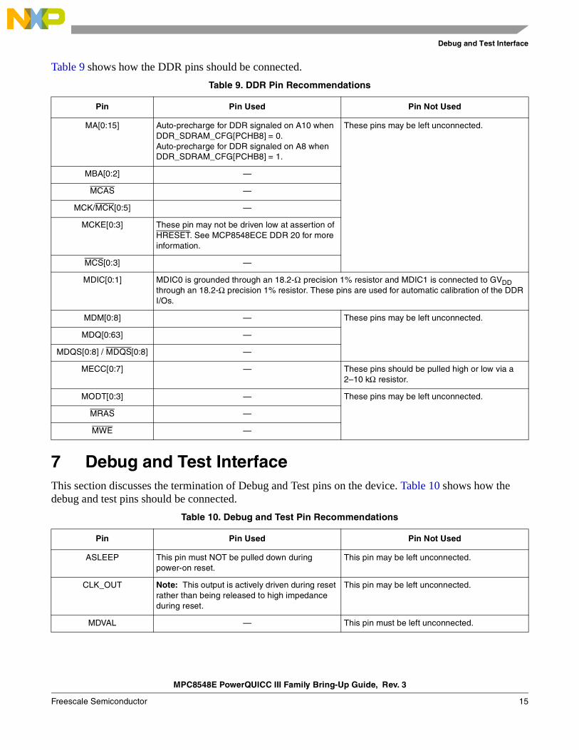
Table 9 shows how the DDR pins should be connected.
7 Debug and Test InterfaceThis section discusses the termination of Debug and Test pins on the device. Table 10 shows how the debug and test pins should be connected.
Table 9. DDR Pin Recommendations
Pin Pin Used Pin Not Used
MA[0:15] Auto-precharge for DDR signaled on A10 when DDR_SDRAM_CFG[PCHB8] = 0. Auto-precharge for DDR signaled on A8 when DDR_SDRAM_CFG[PCHB8] = 1.
These pins may be left unconnected.
MBA[0:2] —
MCAS —
MCK/MCK[0:5] —
MCKE[0:3] These pin may not be driven low at assertion of HRESET. See MCP8548ECE DDR 20 for more information.
MCS[0:3] —
MDIC[0:1] MDIC0 is grounded through an 18.2-Ω precision 1% resistor and MDIC1 is connected to GVDD through an 18.2-Ω precision 1% resistor. These pins are used for automatic calibration of the DDR I/Os.
MDM[0:8] — These pins may be left unconnected.
MDQ[0:63] —
MDQS[0:8] / MDQS[0:8] —
MECC[0:7] — These pins should be pulled high or low via a 2–10 kΩ resistor.
MODT[0:3] — These pins may be left unconnected.
MRAS —
MWE —
Table 10. Debug and Test Pin Recommendations
Pin Pin Used Pin Not Used
ASLEEP This pin must NOT be pulled down during power-on reset.
This pin may be left unconnected.
CLK_OUT Note: This output is actively driven during reset rather than being released to high impedance during reset.
This pin may be left unconnected.
MDVAL — This pin must be left unconnected.
MPC8548E PowerQUICC III Family Bring-Up Guide, Rev. 3
16 Freescale Semiconductor
DMA Interface
8 DMA InterfaceThis section discusses the termination of DMA pins on the device. Table 11 shows how the DMA pins should be connected.
L1_TSTCLK These signals must be pulled up via a 100–1000 Ω resistor to OVDD for normal machine operation.
L2_TSTCLK
LSSD_MODE
MSRCID[0:1] This pin is a reset configuration pin. It has a weak internal pull-up P-FET which is enabled only when the processor is in the reset state.
This pin must be left unconnected.
MSRCID[2:4] These pins must NOT be pulled down during power-on reset.
This pin must be left unconnected.
SD_IMP_CAL_RX This pin must be pulled down through a 200-Ω resistor.
SD_IMP_CAL_TX This pin must be pulled down through a 100-Ω resistor.
SD_PLL_TPA Do not connect.
TEST_SEL This signal must be pulled up via a 100–1000 Ω resistor to OVDD for normal machine operation.
THERM[0:1] — These pins may be left unconnected.
TRIG_IN — Tie low through a 2–10 kΩ resistor to GND.
TRIG_OUT / READY This pin must NOT be pulled down during power-on reset.
This pin must be left unconnected.
Table 11. DMA Pin Recommendations
Pin Pin Used Pin Not Used
DMA_DACK[0:1] This pin is a reset configuration pin that sets the device derivative. These pins require 4.7-kΩ pull-up or pull-down resistors.
DMA_DACK2 / LCS6 — If the Local Bus function of this pin is not used, this output pin may be left floating.
DMA_DACK3 / IRQ10 — Pull high or low to the inactive state through a 2–10 kΩ resistor to OVDD or GND, respectively.
DMA_DREQ[0:1] — Pull high through a 2–10 kΩ resistor to OVDD.
DMA_DREQ2 / LCS5 — If the Local Bus function of this pin is not used, this output pin may be left floating.
DMA_DREQ3 / IRQ9 — Pull high or low to the inactive state through a 2–10 kΩ resistor to OVDD or GND, respectively.
DMA_DDONE[0:1] — These output pins may be left floating.
Table 10. Debug and Test Pin Recommendations (continued)
Pin Pin Used Pin Not Used
MPC8548E PowerQUICC III Family Bring-Up Guide, Rev. 3
Freescale Semiconductor 17
DUART Interface
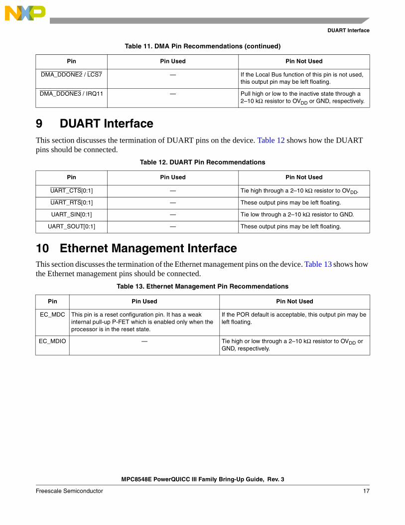
9 DUART InterfaceThis section discusses the termination of DUART pins on the device. Table 12 shows how the DUART pins should be connected.
10 Ethernet Management InterfaceThis section discusses the termination of the Ethernet management pins on the device. Table 13 shows how the Ethernet management pins should be connected.
DMA_DDONE2 / LCS7 — If the Local Bus function of this pin is not used, this output pin may be left floating.
DMA_DDONE3 / IRQ11 — Pull high or low to the inactive state through a 2–10 kΩ resistor to OVDD or GND, respectively.
Table 12. DUART Pin Recommendations
Pin Pin Used Pin Not Used
UART_CTS[0:1] — Tie high through a 2–10 kΩ resistor to OVDD.
UART_RTS[0:1] — These output pins may be left floating.
UART_SIN[0:1] — Tie low through a 2–10 kΩ resistor to GND.
UART_SOUT[0:1] — These output pins may be left floating.
Table 13. Ethernet Management Pin Recommendations
Pin Pin Used Pin Not Used
EC_MDC This pin is a reset configuration pin. It has a weak internal pull-up P-FET which is enabled only when the processor is in the reset state.
If the POR default is acceptable, this output pin may be left floating.
EC_MDIO — Tie high or low through a 2–10 kΩ resistor to OVDD or GND, respectively.
Table 11. DMA Pin Recommendations (continued)
Pin Pin Used Pin Not Used
MPC8548E PowerQUICC III Family Bring-Up Guide, Rev. 3
18 Freescale Semiconductor
eTSEC Interface
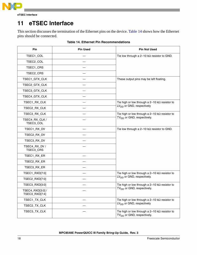
11 eTSEC InterfaceThis section discusses the termination of the Ethernet pins on the device. Table 14 shows how the Ethernet pins should be connected.
Table 14. Ethernet Pin Recommendations
Pin Pin Used Pin Not Used
TSEC1_COL — Tie low through a 2–10 kΩ resistor to GND.
TSEC2_COL —
TSEC1_CRS —
TSEC2_CRS —
TSEC1_GTX_CLK — These output pins may be left floating.
TSEC2_GTX_CLK —
TSEC3_GTX_CLK —
TSEC4_GTX_CLK —
TSEC1_RX_CLK — Tie high or low through a 2–10 kΩ resistor to LVDD or GND, respectively
TSEC2_RX_CLK —
TSEC3_RX_CLK — Tie high or low through a 2–10 kΩ resistor to TVDD or GND, respectively.
TSEC4_RX_CLK / TSEC3_COL
—
TSEC1_RX_DV — Tie low through a 2–10 kΩ resistor to GND.
TSEC2_RX_DV —
TSEC3_RX_DV —
TSEC4_RX_DV / TSEC3_CRS
—
TSEC1_RX_ER —
TSEC2_RX_ER —
TSEC3_RX_ER —
TSEC1_RXD[7:0] — Tie high or low through a 2–10 kΩ resistor to LVDD or GND, respectively.
TSEC2_RXD[7:0] —
TSEC3_RXD[3:0] — Tie high or low through a 2–10 kΩ resistor to TVDD or GND, respectively.
TSEC4_RXD[3:0] / TSEC3_RXD[7:4]
—
TSEC1_TX_CLK — Tie high or low through a 2–10 kΩ resistor to LVDD or GND, respectively
TSEC2_TX_CLK —
TSEC3_TX_CLK — Tie high or low through a 2–10 kΩ resistor to TVDD or GND, respectively.
MPC8548E PowerQUICC III Family Bring-Up Guide, Rev. 3
Freescale Semiconductor 19
I2C Interface
12 I2C InterfaceThis section discusses the termination of I2C pins on the device. Table 15 shows how the I2C pins should be connected.
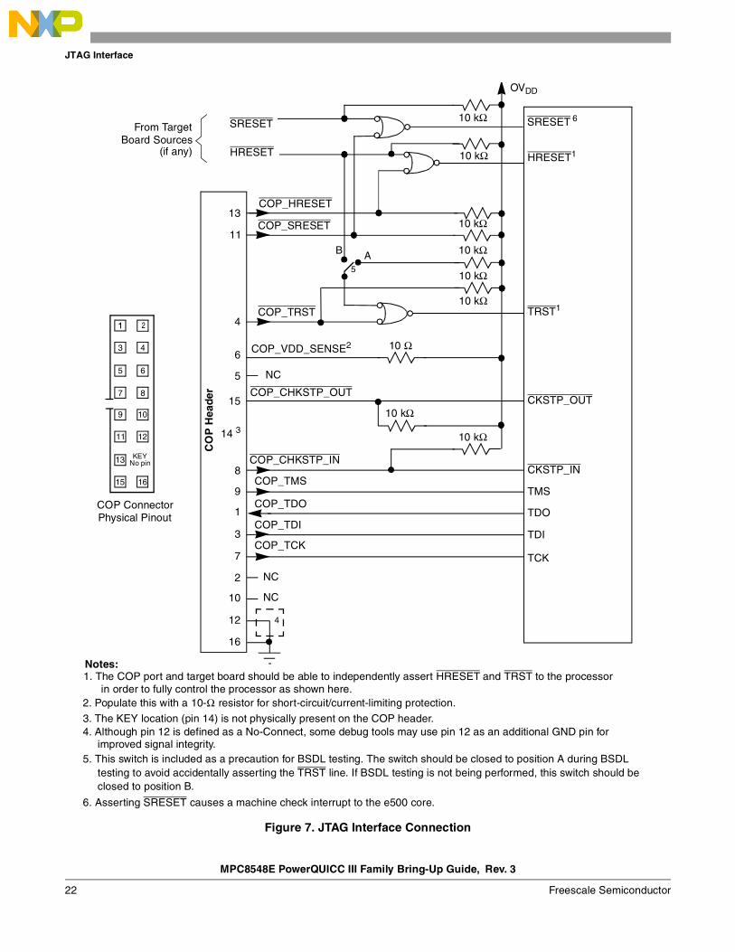
13 JTAG InterfaceCorrect operation of the JTAG interface requires configuration of a group of system control pins as demonstrated in Figure 7. Care must be taken to ensure that these pins are maintained at a valid deasserted state under normal operating conditions as most have asynchronous behavior and spurious assertion may give unpredictable results.
TSEC1_TX_EN These pins require an external 4.7 kΩ pull-down resistor to prevent PHY from seeing a valid Transmit Enable before it is actively driven (during reset).
These output pins may be left floating.
TSEC2_TX_EN
TSEC3_TX_EN
TSEC4_TX_EN / TSEC3_TX_ER
TSEC2_TX_ER This pin is a reset configuration pin. It has a weak internal pull-up P-FET which is enabled only when the processor is in the reset state.
If the POR default is acceptable, this output pin may be left floating.
TSEC1_TX_ER — This output pin may be left floating.
TSEC1_TXD[7:0] This pin is a reset configuration pin. It has a weak internal pull-up P-FET which is enabled only when the processor is in the reset state.
These output pins may be left floating.
TSEC2_TXD[7:0] This pin is a reset configuration pin. It has a weak internal pull-up P-FET which is enabled only when the processor is in the reset state. TSEC2_TXD1 must be valid at Power-Up.
These output pins may be left floating (with the exception of TSEC2_TXD1).
TSEC3_TXD[3:0] This pin is a reset configuration pin. It has a weak internal pull-up P-FET which is enabled only when the processor is in the reset state. The following pins must NOT be pulled down during power-on reset: TSEC3_TXD[3] and TSEC4_TXD3/TSEC3_TXD7.
These output pins may be left floating.
TSEC4_TXD[3:0] / TSEC3_TXD[7:4]
Table 15. I2C Pin Recommendations
Pin Pin Used Pin Not Used
IIC1_SCL Tie these open-drain signals high through a 1-kΩ resistor to OVDD.
Tie high through a 2–10 kΩ resistor to OVDD.
IIC2_SCL
IIC1_SDA
IIC2_SDA
Table 14. Ethernet Pin Recommendations (continued)
Pin Pin Used Pin Not Used
MPC8548E PowerQUICC III Family Bring-Up Guide, Rev. 3
20 Freescale Semiconductor
JTAG Interface
Boundary-scan testing is enabled through the JTAG interface signals. The TRST signal is optional in the IEEE Std 1149.1™ specification, but it is provided on all processors built on Power Architecture technology. The device requires TRST to be asserted during power-on reset flow to ensure that the JTAG boundary logic does not interfere with normal chip operation. While the TAP controller can be forced to the reset state using only the TCK and TMS signals, generally systems assert TRST during the power-on reset flow. Simply tying TRST to HRESET is not practical because the JTAG interface is also used for accessing the common on-chip processor (COP), which implements the debug interface to the chip.
The COP function of these processors allow a remote computer system (typically, a PC with dedicated hardware and debugging software) to access and control the internal operations of the processor. The COP interface connects primarily through the JTAG port of the processor, with some additional status monitoring signals. The COP port requires the ability to independently assert HRESET or TRST in order to fully control the processor. If the target system has independent reset sources, such as voltage monitors, watchdog timers, power supply failures, or push-button switches, then the COP reset signals must be merged into these signals with logic.
The arrangement shown in Figure 7 allows the COP port to independently assert HRESET or TRST, while ensuring that the target can drive HRESET as well.
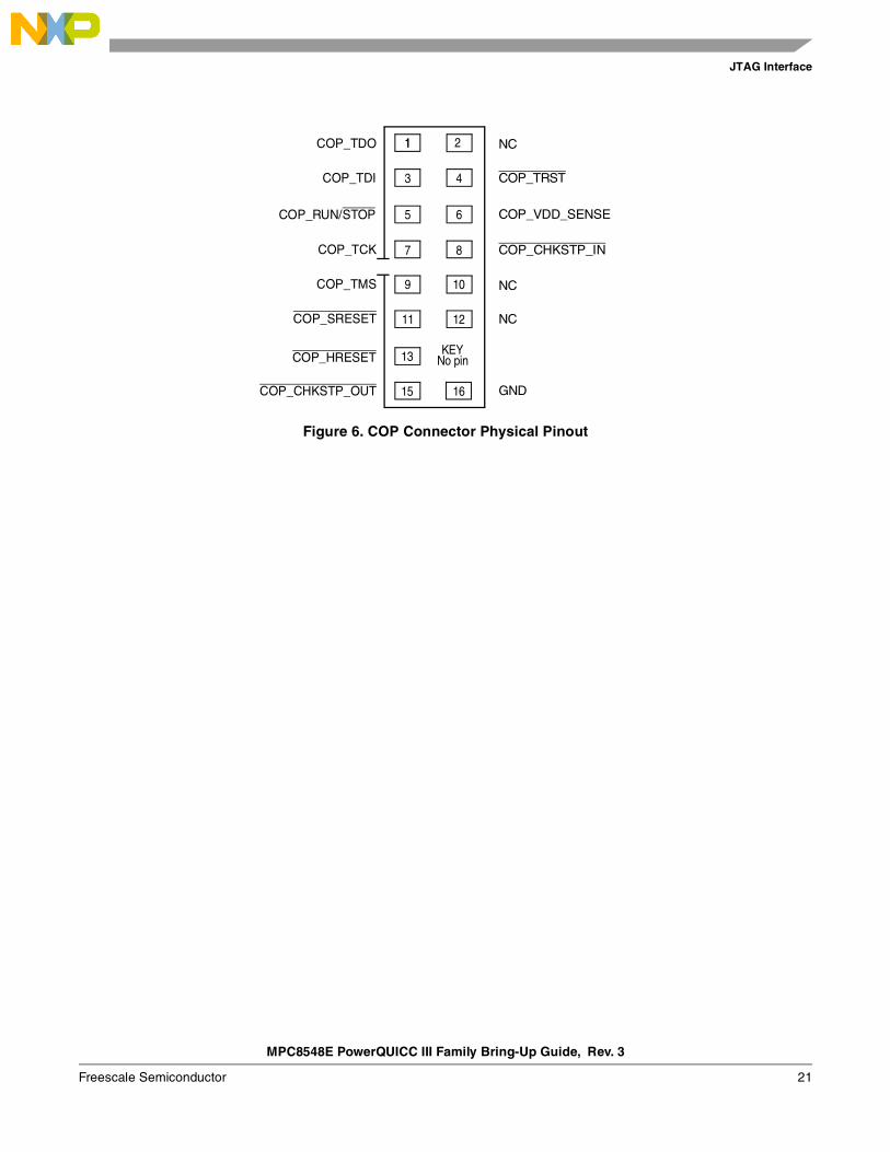
The COP interface has a standard header, shown in Figure 6, for connection to the target system, and is based on the 0.025" square-post, 0.100" centered header assembly (often called a Berg header). The connector typically has pin 14 removed as a connector key.
The COP header adds many benefits such as breakpoints, watchpoints, register and memory examination/modification, and other standard debugger features. An inexpensive option can be to leave the COP header unpopulated until needed.
There is no standardized way to number the COP header; so emulator vendors have issued many different pin numbering schemes. Some COP headers are numbered top-to-bottom then left-to-right, while others use left-to-right then top-to-bottom. Still others number the pins counter-clockwise from pin 1 (as with an IC). Regardless of the numbering scheme, the signal placement recommended in Figure 6 is common to all known emulators.
13.1 Termination of Unused SignalsIf the JTAG interface and COP header is not used, Freescale recommends the following connections:
• TRST should be tied to HRESET through a 0-kΩ isolation resistor so that it is asserted when the system reset signal (HRESET) is asserted, ensuring that the JTAG scan chain is initialized during the power-on reset flow. Freescale recommends that the COP header be designed into the system as shown in Figure 7. If this is not possible, the isolation resistor allows future access to TRST in case a JTAG interface may need to be wired onto the system in future debug situations.
• No pull-up/pull-down is required for TDI, TMS, TDO, or TCK.
MPC8548E PowerQUICC III Family Bring-Up Guide, Rev. 3
Freescale Semiconductor 21
JTAG Interface
Figure 6. COP Connector Physical Pinout
3
13
9
5
1
6
10
15
11
7
16
12
8
4
KEYNo pin
1 2COP_TDO
COP_TDI
COP_RUN/STOP
NC
COP_TRST
COP_VDD_SENSE
COP_CHKSTP_IN
NC
NC
GND
COP_TCK
COP_TMS
COP_SRESET
COP_HRESET
COP_CHKSTP_OUT
MPC8548E PowerQUICC III Family Bring-Up Guide, Rev. 3
22 Freescale Semiconductor
JTAG Interface
Figure 7. JTAG Interface Connection
HRESET
From TargetBoard Sources
COP_HRESET13
COP_SRESET
SRESET
NC
11
COP_VDD_SENSE26
5
15
10 Ω
10 kΩ
10 kΩ
COP_CHKSTP_INCKSTP_IN8
COP_TMS
COP_TDO
COP_TDI
COP_TCK
TMS
TDO
TDI
9
1
3
4COP_TRST
7
16
2
10
12
(if any)
CO
P H
eade
r
14 3
Notes:
3. The KEY location (pin 14) is not physically present on the COP header.
10 kΩ
TRST110 kΩ
10 kΩ
10 kΩ
CKSTP_OUTCOP_CHKSTP_OUT
3
13
9
5
1
6
10
15
11
7
16
12
8
4
KEYNo pin
COP ConnectorPhysical Pinout
1 2
NC
SRESET
2. Populate this with a 10-Ω resistor for short-circuit/current-limiting protection.
NC
OVDD
10 kΩ HRESET1
in order to fully control the processor as shown here.
4. Although pin 12 is defined as a No-Connect, some debug tools may use pin 12 as an additional GND pin for
1. The COP port and target board should be able to independently assert HRESET and TRST to the processor
improved signal integrity.
TCK
4
5
5. This switch is included as a precaution for BSDL testing. The switch should be closed to position A during BSDL testing to avoid accidentally asserting the TRST line. If BSDL testing is not being performed, this switch should be
10 kΩ
6
6. Asserting SRESET causes a machine check interrupt to the e500 core.
AB
closed to position B.
MPC8548E PowerQUICC III Family Bring-Up Guide, Rev. 3
Freescale Semiconductor 23
Local Bus Interface
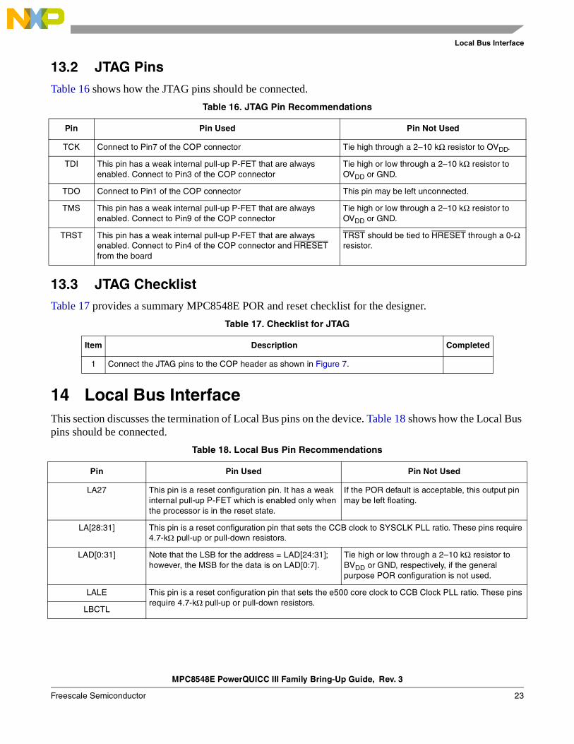
13.2 JTAG PinsTable 16 shows how the JTAG pins should be connected.
13.3 JTAG ChecklistTable 17 provides a summary MPC8548E POR and reset checklist for the designer.
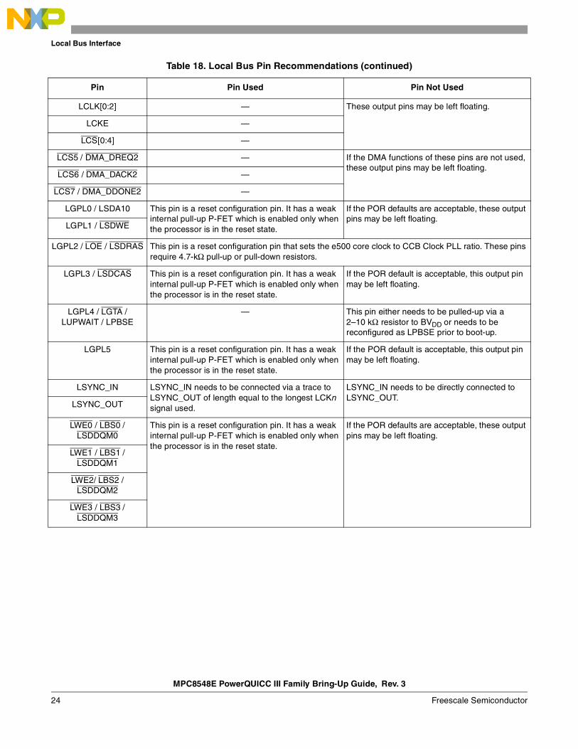
14 Local Bus InterfaceThis section discusses the termination of Local Bus pins on the device. Table 18 shows how the Local Bus pins should be connected.
Table 16. JTAG Pin Recommendations
Pin Pin Used Pin Not Used
TCK Connect to Pin7 of the COP connector Tie high through a 2–10 kΩ resistor to OVDD.
TDI This pin has a weak internal pull-up P-FET that are always enabled. Connect to Pin3 of the COP connector
Tie high or low through a 2–10 kΩ resistor to OVDD or GND.
TDO Connect to Pin1 of the COP connector This pin may be left unconnected.
TMS This pin has a weak internal pull-up P-FET that are always enabled. Connect to Pin9 of the COP connector
Tie high or low through a 2–10 kΩ resistor to OVDD or GND.
TRST This pin has a weak internal pull-up P-FET that are always enabled. Connect to Pin4 of the COP connector and HRESET from the board
TRST should be tied to HRESET through a 0-Ω resistor.
Table 17. Checklist for JTAG
Item Description Completed
1 Connect the JTAG pins to the COP header as shown in Figure 7.
Table 18. Local Bus Pin Recommendations
Pin Pin Used Pin Not Used
LA27 This pin is a reset configuration pin. It has a weak internal pull-up P-FET which is enabled only when the processor is in the reset state.
If the POR default is acceptable, this output pin may be left floating.
LA[28:31] This pin is a reset configuration pin that sets the CCB clock to SYSCLK PLL ratio. These pins require 4.7-kΩ pull-up or pull-down resistors.
LAD[0:31] Note that the LSB for the address = LAD[24:31]; however, the MSB for the data is on LAD[0:7].
Tie high or low through a 2–10 kΩ resistor to BVDD or GND, respectively, if the general purpose POR configuration is not used.
LALE This pin is a reset configuration pin that sets the e500 core clock to CCB Clock PLL ratio. These pins require 4.7-kΩ pull-up or pull-down resistors.
LBCTL
MPC8548E PowerQUICC III Family Bring-Up Guide, Rev. 3
24 Freescale Semiconductor
Local Bus Interface
LCLK[0:2] — These output pins may be left floating.
LCKE —
LCS[0:4] —
LCS5 / DMA_DREQ2 — If the DMA functions of these pins are not used, these output pins may be left floating.
LCS6 / DMA_DACK2 —
LCS7 / DMA_DDONE2 —
LGPL0 / LSDA10 This pin is a reset configuration pin. It has a weak internal pull-up P-FET which is enabled only when the processor is in the reset state.
If the POR defaults are acceptable, these output pins may be left floating.
LGPL1 / LSDWE
LGPL2 / LOE / LSDRAS This pin is a reset configuration pin that sets the e500 core clock to CCB Clock PLL ratio. These pins require 4.7-kΩ pull-up or pull-down resistors.
LGPL3 / LSDCAS This pin is a reset configuration pin. It has a weak internal pull-up P-FET which is enabled only when the processor is in the reset state.
If the POR default is acceptable, this output pin may be left floating.
LGPL4 / LGTA / LUPWAIT / LPBSE
— This pin either needs to be pulled-up via a 2–10 kΩ resistor to BVDD or needs to be reconfigured as LPBSE prior to boot-up.
LGPL5 This pin is a reset configuration pin. It has a weak internal pull-up P-FET which is enabled only when the processor is in the reset state.
If the POR default is acceptable, this output pin may be left floating.
LSYNC_IN LSYNC_IN needs to be connected via a trace to LSYNC_OUT of length equal to the longest LCKn signal used.
LSYNC_IN needs to be directly connected to LSYNC_OUT.
LSYNC_OUT
LWE0 / LBS0 / LSDDQM0
This pin is a reset configuration pin. It has a weak internal pull-up P-FET which is enabled only when the processor is in the reset state.
If the POR defaults are acceptable, these output pins may be left floating.
LWE1 / LBS1 / LSDDQM1
LWE2/ LBS2 / LSDDQM2
LWE3 / LBS3 / LSDDQM3
Table 18. Local Bus Pin Recommendations (continued)
Pin Pin Used Pin Not Used
MPC8548E PowerQUICC III Family Bring-Up Guide, Rev. 3
Freescale Semiconductor 25
PCI Interface
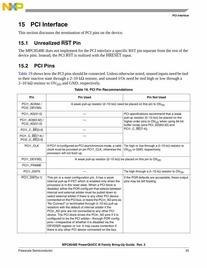
15 PCI InterfaceThis section discusses the termination of PCI pins on the device.
15.1 Unrealized RST PinThe MPC8548E does not implement for the PCI interface a specific RST pin separate from the rest of the device pins. Instead, the PCI RST is realized with the HRESET input.
15.2 PCI PinsTable 19 shows how the PCI pins should be connected. Unless otherwise noted, unused inputs need be tied to their inactive state through a 2–10 kΩ resistor, and unused I/Os need be tied high or low through a 2–10 kΩ resistor to OVDD and GND, respectively.
Table 19. PCI Pin Recommendations
Pin Pin Used Pin Not Used
PCI1_ACK64 / PCI2_DEVSEL
A weak pull-up resistor (2–10 kΩ) need be placed on this pin to OVDD.
PCI1_AD[31:0] — PCI specifications recommend that a weak pull-up resistor (2–10 kΩ) be placed on the higher order pins to OVDD when using 64-bit buffer mode (pins PCI_AD[63:32] and PCI1_C_BE[7:4]).
PCI1_AD[63:32] / PCI2_AD[31:0]
—
PCI1_C_BE[3:0] —
PCI1_C_BE[7:4] / PCI2_C_BE[3:0]
—
PCI1_CLK If PCI1 is configured as PCI asynchronous mode, a valid clock must be provided on pin PCI1_CLK, otherwise the processor will not boot up.
Tie high or low through a 2–10 kΩ resistor to OVDD or GND, respectively,
PCI1_DEVSEL A weak pull-up resistor (2–10 kΩ) be placed on this pin to OVDD.
PCI1_FRAME
PCI1_GNT0 — Tie high through a 2–10 kΩ resistor to OVDD.
PCI1_GNT[4:1] This pin is a reset configuration pin. It has a weak internal pull-up P-FET which is enabled only when the processor is in the reset state. When a PCI block is disabled, either the POR config pin that selects between internal and external arbiter must be pulled down to select external arbiter if there is any other PCI device connected on the PCI bus, or leave the PCIn_AD pins as “No Connect” or terminated through 2–10 kΩ pull-up resistors with the default of internal arbiter if the PCIn_AD pins are not connected to any other PCI device. The PCI block drives the PCIn_AD pins if it is configured to be the PCI arbiter—through POR config pins—irrespective of whether it is disabled via the DEVDISR register or not. It may cause contention if there is any other PCI device connected on the bus.
If the POR defaults are acceptable, these output pins may be left floating.
MPC8548E PowerQUICC III Family Bring-Up Guide, Rev. 3
26 Freescale Semiconductor
PCI Interface
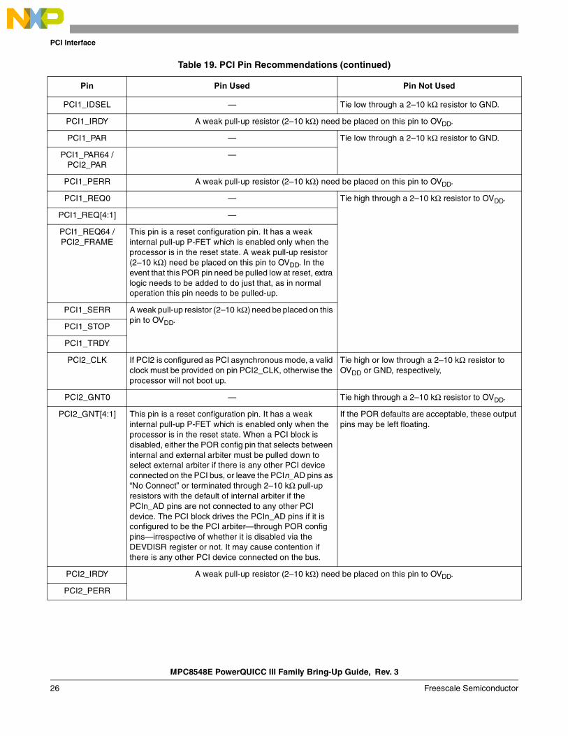
PCI1_IDSEL — Tie low through a 2–10 kΩ resistor to GND.
PCI1_IRDY A weak pull-up resistor (2–10 kΩ) need be placed on this pin to OVDD.
PCI1_PAR — Tie low through a 2–10 kΩ resistor to GND.
PCI1_PAR64 / PCI2_PAR
—
PCI1_PERR A weak pull-up resistor (2–10 kΩ) need be placed on this pin to OVDD.
PCI1_REQ0 — Tie high through a 2–10 kΩ resistor to OVDD.
PCI1_REQ[4:1] —
PCI1_REQ64 / PCI2_FRAME
This pin is a reset configuration pin. It has a weak internal pull-up P-FET which is enabled only when the processor is in the reset state. A weak pull-up resistor (2–10 kΩ) need be placed on this pin to OVDD. In the event that this POR pin need be pulled low at reset, extra logic needs to be added to do just that, as in normal operation this pin needs to be pulled-up.
PCI1_SERR A weak pull-up resistor (2–10 kΩ) need be placed on this pin to OVDD.
PCI1_STOP
PCI1_TRDY
PCI2_CLK If PCI2 is configured as PCI asynchronous mode, a valid clock must be provided on pin PCI2_CLK, otherwise the processor will not boot up.
Tie high or low through a 2–10 kΩ resistor to OVDD or GND, respectively,
PCI2_GNT0 — Tie high through a 2–10 kΩ resistor to OVDD.
PCI2_GNT[4:1] This pin is a reset configuration pin. It has a weak internal pull-up P-FET which is enabled only when the processor is in the reset state. When a PCI block is disabled, either the POR config pin that selects between internal and external arbiter must be pulled down to select external arbiter if there is any other PCI device connected on the PCI bus, or leave the PCIn_AD pins as “No Connect” or terminated through 2–10 kΩ pull-up resistors with the default of internal arbiter if the PCIn_AD pins are not connected to any other PCI device. The PCI block drives the PCIn_AD pins if it is configured to be the PCI arbiter—through POR config pins—irrespective of whether it is disabled via the DEVDISR register or not. It may cause contention if there is any other PCI device connected on the bus.
If the POR defaults are acceptable, these output pins may be left floating.
PCI2_IRDY A weak pull-up resistor (2–10 kΩ) need be placed on this pin to OVDD.
PCI2_PERR
Table 19. PCI Pin Recommendations (continued)
Pin Pin Used Pin Not Used
MPC8548E PowerQUICC III Family Bring-Up Guide, Rev. 3
Freescale Semiconductor 27
PIC Interface
16 PIC InterfaceThis section discusses the termination of PIC pins on the device. Table 20 shows how the PIC pins should be connected.
17 SerDes InterfaceThis section discusses the termination of SerDes pins on the device. Table 21 shows how the SerDes pins should be connected.
PCI2_REQ0 — Tie high through a 2–10 kΩ resistor to OVDD.
PCI2_REQ[4:1] —
PCI2_SERR A weak pull-up resistor (2–10 kΩ) need be placed on this pin to OVDD.
PCI2_STOP
PCI2_TRDY
Table 20. PIC Pin Recommendations
Pin Pin Used Pin Not Used
IRQ[0:8] A weak pull-up or pull-down may be needed to the inactive state.
Tie high or low to the inactive state through a 2–10 kΩ resistor to OVDD or GND, respectively,
IRQ9 / DMA_DREQ3
IRQ10 / DMA_DACK3
IRQ11 / DMA_DDONE3
IRQ_OUT Pull high through a 2–10 kΩ resistor to OVDD.
MCP
UDE
Table 21. SerDes Pin Recommendations
Pin Pin Used Pin Not Used
SD_PLL_TPD Do not connect.
SD_RX[0:7] — These pins must be connected to GND.
SD_RX[0:7] —
SD_TX[0:7] If these pins are used for PCI Express, AC coupling capacitors need to be placed at the outputs.
These pins must be left unconnected.
SD_TX[0:7]
Table 19. PCI Pin Recommendations (continued)
Pin Pin Used Pin Not Used
MPC8548E PowerQUICC III Family Bring-Up Guide, Rev. 3
28 Freescale Semiconductor
System Control
18 System ControlThis section discusses the termination of System Control pins on the device. Table 22 shows how the System Control pins should be connected.
19 Reserved PinsSeveral pins on the MPC8548E are marked RESERVED. Table 23 shows how the SerDes pins should be connected.
Table 22. System Control Pin Recommendations
Pin Pin Used Pin Not Used
CKSTP_IN Pull high through a 2–10 kΩ resistor to OVDD. Connect to Pin7 of the COP connector (refer to Figure 7).
Pull high through a 2–10 kΩ resistor to OVDD.
CKSTP_OUT Pull this open-drain signal high through a 2–10 kΩ resistor to OVDD. Connect to Pin15 of the COP connector (refer to Figure 7).
This pin may be left unconnected.
HRESET Pull high through a 2–10 kΩ resistor to OVDD. Connect to Pin13 of the COP connector (refer to Figure 7).
HRESET_REQ Pull high through a 2–10 kΩ resistor to OVDD. This pin must NOT be pulled down during power-on reset.
This pin must NOT be pulled down during power-on reset.
SRESET Pull high through a 2–10 kΩ resistor to OVDD. Connect to Pin11 of the COP connector (refer to Figure 7).
Pull high through a 2–10 kΩ resistor to OVDD.
Table 23. RESERVED Pin Recommendations
Pin Number Comment
AC1 Pull high through a 2–10 kΩ resistor to OVDD.
AC3
M20 These pins must be left unconnected.
M21
M25 This pin should be pulled to ground through a 300-Ω (±10%) resistor.
M26 This pin should be connected to XVDD.
T22 These pins must be left unconnected.
T23
V27 This pin should be pulled to ground through a 300-Ω (±10%) resistor.
V28 This pin should be connected to XVDD.
MPC8548E PowerQUICC III Family Bring-Up Guide, Rev. 3
Freescale Semiconductor 29
Power and Ground Signals
20 Power and Ground SignalsThe MPC8548E has several power supplies. Table 24 shows how the SerDes pins should be connected.
21 Revision HistoryTable 25 provides a revision history for this application note.
Table 24. Power and Ground Pin Recommendations
Pin Comment
AVDD_CORE Power supply for e500 PLL (1.1 V through a filter).
AVDD_LBIU Power supply for Local Bus PLL (1.1 V through a filter).
AVDD_PCI1 Power supply for PCI1 PLL (1.1 V through a filter).
AVDD_PCI2 Power supply for PCI2 PLL (1.1 V through a filter).
AVDD_PLAT Power supply for core complex bus PLL. (1.1 V through a filter)
AVDD_SRDS Power supply for SerDes PLL (1.1 V through a filter).
BVDD Power supply for the Local Bus I/Os (2.5 V / 3.3 V).
GND Power supply for the DDR I/Os (1.8 V / 2.5 V).
GVDD Power supply for the DDR I/Os (1.8 V / 2.5 V).
LVDD Power supply for the TSEC1 and TSEC2 I/Os (2.5 V / 3.3 V).
MVREF DDR input reference voltage equal to approximately half of GVDD
OVDD Power supply for PCI and other standards’ I/Os (3.3 V).
SENSEVDD This pin is connected to the VDD plane internally and may be used by the core power supply to improve tracking and regulation.
SENSEVSS This pin is connected to the GND plane internally and may be used by the core power supply to improve tracking and regulation.
SVDD Power supply for the SerDes transceivers (1.1 V).
TVDD Power supply for the TSEC3 and TSEC4 I/Os (2.5 V / 3.3 V).
XVDD Power supply for the SerDes I/Os (1.1 V).
VDD Power supply the core I/Os (1.1 V).
Table 25. Document Revision History
Revision Date Substantive Change(s)
3 07/2010 • In Section 2.1, “Power Supplies,” for the list above the note, changed the second item from “2.5 V for RGMII, RTBI, or FIFO modes of operation” to “2.5 V for GMII, RGMII, RTBI, or FIFO modes of operation.”
• Added note in Section 6, “DDR Interface,” to disable unused clocks.
2 07/2009 • Added IO power guideline on Section 2.3, “I/O Power Dissipation.” • Removed ref to use 0.01uF or 0.1uF in Section 2.6, “Power Supply Decoupling.”
MPC8548E PowerQUICC III Family Bring-Up Guide, Rev. 3
30 Freescale Semiconductor
Revision History
1 10/2008 • Updated Section 4.2, “Pin Map,” to change “top view of the pin map” to “bottom view of the pin map.” • In Section 16, “PIC Interface,” changed PCI to PIC in first sentence. • Updated part number column in Table 5, “MPC8548E Derivatives.”
0 06/2008 Initial release.
Table 25. Document Revision History (continued)
Revision Date Substantive Change(s)
MPC8548E PowerQUICC III Family Bring-Up Guide, Rev. 3
Freescale Semiconductor 31
Revision History
THIS PAGE INTENTIONALLY LEFT BLANK
Document Number: AN3640Rev. 308/2010
Information in this document is provided solely to enable system and software
implementers to use Freescale Semiconductor products. There are no express or
implied copyright licenses granted hereunder to design or fabricate any integrated
circuits or integrated circuits based on the information in this document.
Freescale Semiconductor reserves the right to make changes without further notice to
any products herein. Freescale Semiconductor makes no warranty, representation or
guarantee regarding the suitability of its products for any particular purpose, nor does
Freescale Semiconductor assume any liability arising out of the application or use of
any product or circuit, and specifically disclaims any and all liability, including without
limitation consequential or incidental damages. “Typical” parameters which may be
provided in Freescale Semiconductor data sheets and/or specifications can and do
vary in different applications and actual performance may vary over time. All operating
parameters, including “Typicals” must be validated for each customer application by
customer’s technical experts. Freescale Semiconductor does not convey any license
under its patent rights nor the rights of others. Freescale Semiconductor products are
not designed, intended, or authorized for use as components in systems intended for
surgical implant into the body, or other applications intended to support or sustain life,
or for any other application in which the failure of the Freescale Semiconductor product
could create a situation where personal injury or death may occur. Should Buyer
purchase or use Freescale Semiconductor products for any such unintended or
unauthorized application, Buyer shall indemnify and hold Freescale Semiconductor
and its officers, employees, subsidiaries, affiliates, and distributors harmless against all
claims, costs, damages, and expenses, and reasonable attorney fees arising out of,
directly or indirectly, any claim of personal injury or death associated with such
unintended or unauthorized use, even if such claim alleges that Freescale
Semiconductor was negligent regarding the design or manufacture of the part.
How to Reach Us:
Home Page: www.freescale.com
Web Support: http://www.freescale.com/support
USA/Europe or Locations Not Listed: Freescale Semiconductor, Inc.Technical Information Center, EL5162100 East Elliot Road Tempe, Arizona 85284 1-800-521-6274 or+1-480-768-2130www.freescale.com/support
Europe, Middle East, and Africa:Freescale Halbleiter Deutschland GmbHTechnical Information CenterSchatzbogen 781829 Muenchen, Germany+44 1296 380 456 (English) +46 8 52200080 (English)+49 89 92103 559 (German)+33 1 69 35 48 48 (French) www.freescale.com/support
Japan: Freescale Semiconductor Japan Ltd. HeadquartersARCO Tower 15F1-8-1, Shimo-Meguro, Meguro-ku Tokyo 153-0064Japan 0120 191014 or+81 3 5437 [email protected]
Asia/Pacific: Freescale Semiconductor China Ltd. Exchange Building 23FNo. 118 Jianguo RoadChaoyang DistrictBeijing 100022China+86 10 5879 [email protected]
For Literature Requests Only:Freescale Semiconductor
Literature Distribution Center 1-800 441-2447 or+1-303-675-2140Fax: +1-303-675-2150LDCForFreescaleSemiconductor
@hibbertgroup.com
Freescale and the Freescale logo are trademarks or registered trademarks of Freescale Semiconductor, Inc. in the U.S. and other countries. All other product or service names are the property of their respective owners. The Power Architecture and Power.org word marks and the Power and Power.org logos and related marks are trademarks and service marks licensed by Power.org. IEEE 1149.1 is a registered trademark of the Institute of Electrical and Electronics Engineers, Inc. (IEEE). This product is not endorsed or approved by the IEEE.
© 2010 Freescale Semiconductor, Inc