Embed Size (px)
Citation preview

Advance Information
MPC7410RXPCPNS/DRev. 1, 10/2002
MPC7410 Part Number Specification for theMPC7410RXnnnPC Series
Motorola PartNumbers Affected:
XPC7410RX400PCXPC7410RX450PCXPC7410RX500PCXPC7410RX550PC
F
ree
sca
le S
em
ico
nd
uc
tor,
I
Freescale Semiconductor, Inc.n
c..
.
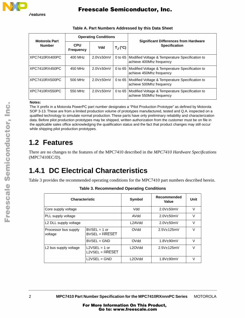
This document describes part number specific changes to recommended operating conditionsand revised electrical specifications, as applicable, from those described in the generalMPC7410 Hardware Specifications (order #: MPC7410EC/D).
Specifications provided in this Part Number Specification supersede those in the MPC7410Hardware Specifications, for the part numbers listed in Table A only, specifications notaddressed herein are unchanged. This document is frequently updated. Therefore, contactyour Motorola sales office for the latest version.
Part numbers addressed in this document are listed in Table A. For more detailed orderinginformation see, Table 17.
For More Information On This Product,
Go to: www.freescale.com
Features
Fre
esc
ale
Se
mic
on
du
cto
r, I
Freescale Semiconductor, Inc.n
c..
.
1.2 FeaturesThere are no changes to the features of the MPC7410 described in the MPC7410 Hardware Specifications(MPC7410EC/D).
1.4.1 DC Electrical CharacteristicsTable 3 provides the recommended operating conditions for the MPC7410 part numbers described herein.
Table A. Part Numbers Addressed by this Data Sheet
Motorola Part Number
Operating ConditionsSignificant Differences from Hardware
SpecificationCPU Frequency
Vdd TJ (°C)
XPC7410RX400PC 400 MHz 2.0V±50mV 0 to 65 Modified Voltage & Temperature Specification to achieve 400Mhz frequency
XPC7410RX450PC 450 MHz 2.0V±50mV 0 to 65 Modified Voltage & Temperature Specification to achieve 450Mhz frequency
XPC7410RX500PC 500 MHz 2.0V±50mV 0 to 65 Modified Voltage & Temperature Specification to achieve 500Mhz frequency
XPC7410RX550PC 550 MHz 2.0V±50mV 0 to 65 Modified Voltage & Temperature Specification to achieve 550Mhz frequency
Notes: The X prefix in a Motorola PowerPC part number designates a “Pilot Production Prototype” as defined by Motorola SOP 3-13. These are from a limited production volume of prototypes manufactured, tested and Q.A. inspected on a qualified technology to simulate normal production. These parts have only preliminary reliability and characterization data. Before pilot production prototypes may be shipped, written authorization from the customer must be on file in the applicable sales office acknowledging the qualification status and the fact that product changes may still occur while shipping pilot production prototypes.
Table 3. Recommended Operating Conditions
Characteristic SymbolRecommended
ValueUnit
Core supply voltage Vdd 2.0V±50mV V
PLL supply voltage AVdd 2.0V±50mV V
L2 DLL supply voltage L2AVdd 2.0V±50mV V
Processor bus supply voltage
BVSEL = 1 orBVSEL = HRESET
OVdd 2.5V±125mV V
BVSEL = GND OVdd 1.8V±90mV V
L2 bus supply voltage L2VSEL = 1 orL2VSEL = HRESET
L2OVdd 2.5V±125mV V
L2VSEL = GND L2OVdd 1.8V±90mV V
2 MPC7410 Part Number Specification for the MPC7410RXnnnPC Series MOTOROLA
For More Information On This Product, Go to: www.freescale.com

DC Electrical Characteristics
Fre
esc
ale
Se
mic
on
du
cto
r, I
Freescale Semiconductor, Inc.n
c..
.
Table 6 provides the power consumption for the MPC7410 part at the frequencies described herein.
Input voltage Processor bus Vin GND to OVdd V
L2 Bus Vin GND to L2OVdd V
JTAG Signals Vin GND to OVdd V
Die-junction temperature Tj 0-65 °C
Note: These are the recommended and tested operating conditions. Proper device operation outside of these conditions is not guaranteed.
Table 6. Power Consumption for MPC7410
Processor (CPU)
Frequency
Processor (CPU)
Frequency Unit Notes
400Mhz 500Mhz
Full-On Mode
Typical
Maximum
6 7 W 1, 3,
12 14 W 1, 2, 4
Doze Mode
Maximum 4 5 W 1, 2
Nap Mode
Maximum 2.0 2.25 W 1, 2
Sleep Mode
Maximum 2.0 2.25 W 1, 2
Sleep Mode—PLL and DLL Disabled
Typical 0.5 0.5 W 1, 3
Maximum 2.0 2.0 W 1, 2
Notes: 1. These values apply for all valid processor bus and L2 bus ratios. The values
do not include I/O Supply Power (OVdd and L2OVdd) or PLL/DLL supply power (AVdd and L2AVdd). OVdd and L2OVdd power is system dependent, but is typically <10% of Vdd power. Worst case power consumption for AVdd = 15 mw and L2AVdd = 15 mW.
2. Maximum power is measured at Vdd = 2.2V while running an entirely cache-resident, contrived sequence of instructions which keep the execution units, including AltiVec, maximally busy.
3. Typical power is an average value measured at Vdd = AVdd = L2AVdd = 2.15V, OVdd = L2OVdd = 2.5V in a system while running a codec application that is AltiVec intensive.
4. These values include the use of Altivec. Without Altivec operation, estimate a 25% decrease.
Table 3. Recommended Operating Conditions (continued)
Characteristic SymbolRecommended
ValueUnit
MOTOROLA MPC7410 Part Number Specification for the MPC7410RXnnnPC Series 3
For More Information On This Product, Go to: www.freescale.com

DC Electrical Characteristics
Fre
esc
ale
Se
mic
on
du
cto
r, I
Freescale Semiconductor, Inc.n
c..
.
1.4.2.1 Clock AC SpecificationsTable 7 provides the additional clock AC timing specifications described in this Part Number Specification.Refer to the MPC7410 Hardware Specification for the remaining frequencies.
Table 7. Clock AC Timing Specifications
At recommended operating conditions (See Table 3)
Characteristic Symbol400 MHz 450 MHz 500 MHz 550 MHz
Unit NotesMin Max Min Max Min Max Min Max
Processor frequency
fcore 300 400 300 450 300 500 300 550 MHz
VCO frequency fVCO 600 800 600 900 600 1000 600 1100 MHz
SYSCLK frequency fSYSCLK 33 100 33 100 33 100 33 100 MHz 1
SYSCLK cycle time tSYSCLK 10 30 10 30 10 30 10 30 ns
SYSCLK rise and fall time
tKR & tKF — 1.0 — 1.0 — 1.0 — 1.0 ns 2
— 0.5 — 0.5 — 0.5 — 0.5 ns 3
SYSCLK duty cycle measured at OVdd/2
tKHKL/tSYS
CLK
40 60 40 60 40 60 40 60 % 4
SYSCLK jitter — ±150 — ±150 — ±150 — ±150 ps 5
Internal PLL relock time
— 100 — 100 — 100 — 100 µs 6
Note:See general hardware specification.
4 MPC7410 Part Number Specification for the MPC7410RXnnnPC Series MOTOROLA
For More Information On This Product, Go to: www.freescale.com
DC Electrical Characteristics
Fre
esc
ale
Se
mic
on
du
cto
r, I
Freescale Semiconductor, Inc.n
c..
.
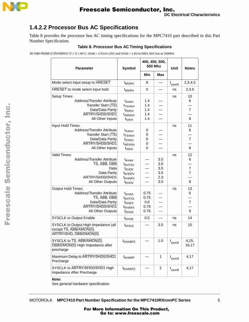
1.4.2.2 Processor Bus AC SpecificationsTable 8 provides the processor bus AC timing specifications for the MPC7410 part described in this PartNumber Specification.
Table 8. Processor Bus AC Timing Specifications
At Vdd=AVdd=2.0V±50mV; 0 ≤ Tj ≤ 65°C, OVdd = 2.5V±0.125V and OVdd = 1.8V±0.090V, 60X bus at 100MHz
Parameter Symbol
400, 450, 500, 550 Mhz Unit Notes
Min Max
Mode select input setup to HRESET tMVRH 8 — tsysclk
2,3,4,5
HRESET to mode select input hold tMXRH 0 — ns 2,3,5
Setup Times:Address/Transfer Attribute
Transfer Start (TS)Data/Data Parity
ARTRY/SHD0/SHD1All Other Inputs
tAVKHtTSVKHtDVKHtARVKHtIVKH
1.41.41.41.41.4
—————
ns 106—7—8
Input Hold Times:Address/Transfer Attribute
Transfer Start (TS)Data/Data Parity
ARTRY/SHD0/SHD1All Other Inputs
tAXKHtTSXKHtDXKHtARXKHtIXKH
00000
—————
ns 116—7—8
Valid Times: Address/Transfer Attribute
TS, ABB, DBBData
Data ParityARTRY/SHD0/SHD1
All Other Outputs
tKHAVtKHTSVtKHDV
tKHDPVtKHARVtKHOV
——————
3.03.03.53.52.33.0
ns 126—77—9
Output Hold Times:Address/Transfer Attribute
TS, ABB, DBBData/Data Parity
ARTRY/SHD0/SHD1All Other Outputs
tKHAXtKHTSXtKHDXtKHARXtKHOX
0.750.750.60.750.75
—————
ns 136—7—9
SYSCLK to Output Enable tKHOE 0.5 — ns 14
SYSCLK to Output High Impedance (all except TS, ABB/AMON(0), ARTRY/SHD, DBB/DMON(0)
tKHOZ — 3.5 ns 15
SYSCLK to TS, ABB/AMON(0), DBB/DMON(0) High Impedance after precharge
tKHABPZ — 1.0 tsysclk
4,15, 16,17
Maximum Delay to ARTRY/SHD0/SHD1 Precharge
tKHARP — 1 tsysclk
4,17
SYSCLK to ARTRY/SHD0/SHD1 High Impedance After Precharge
tKHARPZ — 2 tsysclk
4,17
Note:See general hardware specification.
MOTOROLA MPC7410 Part Number Specification for the MPC7410RXnnnPC Series 5
For More Information On This Product, Go to: www.freescale.com
DC Electrical Characteristics
Fre
esc
ale
Se
mic
on
du
cto
r, I
Freescale Semiconductor, Inc.n
c..
.
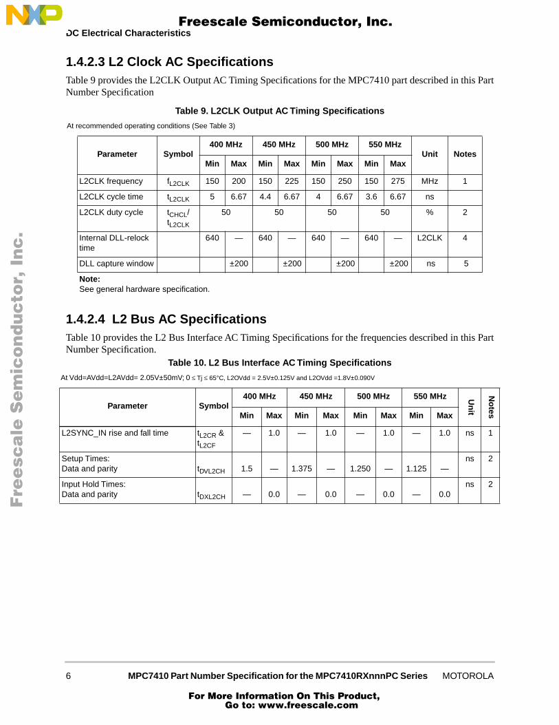
1.4.2.3 L2 Clock AC SpecificationsTable 9 provides the L2CLK Output AC Timing Specifications for the MPC7410 part described in this PartNumber Specification
1.4.2.4 L2 Bus AC SpecificationsTable 10 provides the L2 Bus Interface AC Timing Specifications for the frequencies described in this PartNumber Specification.
Table 9. L2CLK Output AC Timing Specifications
At recommended operating conditions (See Table 3)
Parameter Symbol400 MHz 450 MHz 500 MHz 550 MHz
Unit NotesMin Max Min Max Min Max Min Max
L2CLK frequency fL2CLK 150 200 150 225 150 250 150 275 MHz 1
L2CLK cycle time tL2CLK 5 6.67 4.4 6.67 4 6.67 3.6 6.67 ns
L2CLK duty cycle tCHCL/tL2CLK
50 50 50 50 % 2
Internal DLL-relock time
640 — 640 — 640 — 640 — L2CLK 4
DLL capture window ±200 ±200 ±200 ±200 ns 5
Note: See general hardware specification.
Table 10. L2 Bus Interface AC Timing Specifications
At Vdd=AVdd=L2AVdd= 2.05V±50mV; 0 ≤ Tj ≤ 65°C, L2OVdd = 2.5V±0.125V and L2OVdd =1.8V±0.090V
Parameter Symbol400 MHz 450 MHz 500 MHz 550 MHz U
nit
No
tesMin Max Min Max Min Max Min Max
L2SYNC_IN rise and fall time tL2CR & tL2CF
— 1.0 — 1.0 — 1.0 — 1.0 ns 1
Setup Times:Data and parity tDVL2CH 1.5 — 1.375 — 1.250 — 1.125 —
ns 2
Input Hold Times:Data and parity tDXL2CH — 0.0 — 0.0 — 0.0 — 0.0
ns 2
6 MPC7410 Part Number Specification for the MPC7410RXnnnPC Series MOTOROLA
For More Information On This Product, Go to: www.freescale.com

Document Revision History
F
ree
sca
le S
em
ico
nd
uc
tor,
I
Freescale Semiconductor, Inc.n
c..
.
1.9 Document Revision HistoryTable Table 16. provides a revision history for this Part Number Specification.
1.10 Ordering Information
1.10.1 Part Numbers Addressed by this SpecificationTable 17 provides the ordering information for the MPC7410 part described in this document.
Valid Times:All outputs when L2CR[14-15] = 00All outputs when L2CR[14-15] = 01All outputs when L2CR[14-15] = 10All outputs when L2CR[14-15] = 11
tL2CHOV----
2.5TBDTBDTBD
----
2.375TBDTBDTBD
----
2.25TBDTBDTBD
----
2.05TBDTBDTBD
ns 3,4
Output Hold TimesAll outputs when L2CR[14-15] = 00All outputs when L2CR[14-15] = 01All outputs when L2CR[14-15] = 10All outputs when L2CR[14-15] = 11
tL2CHOX0.6
TBDTBDTBD
----
0.55TBDTBDTBD
----
0.5TBDTBDTBD
----
0.45TBDTBDTBD
----
ns 3
L2SYNC_IN to high impedanceAll outputs when L2CR[14-15] = 00All outputs when L2CR[14-15] = 01All outputs when L2CR[14-15] = 10All outputs when L2CR[14-15] = 11
tL2CHOZ----
2.02.53.03.5
----
2.02.53.03.5
----
2.02.53.03.5
----
2.02.53.03.5
ns
Note:See general hardware specification.
Table 16. Document Revision History
Document Revision Substantive Changes
Rev 0 Initial Release
Rev 1 Minor reformatting.
Section 1.10.1 - added Table 17, Part Marking Nomenclature
Table 10. L2 Bus Interface AC Timing Specifications (continued)
At Vdd=AVdd=L2AVdd= 2.05V±50mV; 0 ≤ Tj ≤ 65°C, L2OVdd = 2.5V±0.125V and L2OVdd =1.8V±0.090V
Parameter Symbol400 MHz 450 MHz 500 MHz 550 MHz U
nit
No
tesMin Max Min Max Min Max Min Max
MOTOROLA MPC7410 Part Number Specification for the MPC7410RXnnnPC Series 7
For More Information On This Product, Go to: www.freescale.com
Ordering Information
F
ree
sca
le S
em
ico
nd
uc
tor,
I
Freescale Semiconductor, Inc.n
c..
.
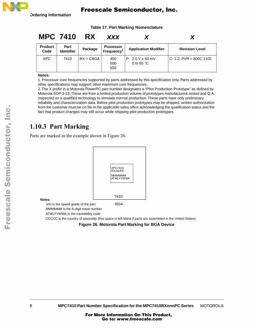
Table 17. Part Marking Nomenclature
1.10.3 Part MarkingParts are marked as the example shown in Figure 26.
Figure 26. Motorola Part Marking for BGA Device
MPC 7410 RX xxx x xProduct
CodePart
IdentifierPackage
Processor Frequency1 Application Modifier Revision Level
XPC 7410 RX = CBGA 450500550
P: 2.0 V ± 50 mV 0 to 65 °C
C: 1.2; PVR = 800C 1102
Notes: 1. Processor core frequencies supported by parts addressed by this specification only. Parts addressed by other specifications may support other maximum core frequencies.2. The X prefix in a Motorola PowerPC part number designates a “Pilot Production Prototype” as defined by Motorola SOP 3-13. These are from a limited production volume of prototypes manufactured, tested and Q.A. inspected on a qualified technology to simulate normal production. These parts have only preliminary reliability and characterization data. Before pilot production prototypes may be shipped, written authorization from the customer must be on file in the applicable sales office acknowledging the qualification status and the fact that product changes may still occur while shipping pilot production prototypes.
BGANotes:
CCCCC is the country of assembly (this space is left blank if parts are assembled in the United States)
MMMMMM is the 6-digit mask number
ATWLYYWWA is the traceability code
XPC7410RXnnnPC
MMMMMMATWLYYWWA
7410
nnn is the speed grade of the part
8 MPC7410 Part Number Specification for the MPC7410RXnnnPC Series MOTOROLA
For More Information On This Product, Go to: www.freescale.com
Ordering Information
F
ree
sca
le S
em
ico
nd
uc
tor,
I
Freescale Semiconductor, Inc.n
c..
.
MOTOROLA MPC7410 Part Number Specification for the MPC7410RXnnnPC Series 9
For More Information On This Product, Go to: www.freescale.com
10 MPC7410 Part Number Specification for the MPC7410RXnnnPC Series MOTOROLA
Ordering Information
Fre
esc
ale
Se
mic
on
du
cto
r, I
Freescale Semiconductor, Inc.
For More Information On This Product, Go to: www.freescale.com
nc
...

MOTOROLA MPC7410 Part Number Specification for the MPC7410RXnnnPC Series 11
Ordering Information
Fre
esc
ale
Se
mic
on
du
cto
r, I
Freescale Semiconductor, Inc.
For More Information On This Product, Go to: www.freescale.com
nc
...
MPC7410RXPCPNS/D
HOW TO REACH US:
USA/EUROPE/LOCATIONS NOT LISTED:
Motorola Literature Distribution P.O. Box 5405, Denver, Colorado 80217 1-303-675-2140 or 1-800-441-2447
JAPAN:
Motorola Japan Ltd. SPS, Technical Information Center 3-20-1, Minami-Azabu Minato-ku Tokyo 106-8573 Japan81-3-3440-3569
ASIA/PACIFIC:
Motorola Semiconductors H.K. Ltd. Silicon Harbour Centre, 2 Dai King Street Tai Po Industrial Estate, Tai Po, N.T., Hong Kong852-26668334
TECHNICAL INFORMATION CENTER:
1-800-521-6274
HOME PAGE:
http://www.motorola.com/semiconductors
DOCUMENT COMMENTS:
FAX (512) 933-2625 Attn: RISC Applications Engineering
Information in this document is provided solely to enable system and software implementers to use
Motorola products. There are no express or implied copyright licenses granted hereunder to design
or fabricate any integrated circuits or integrated circuits based on the information in this document.
Motorola reserves the right to make changes without further notice to any products herein.
Motorola makes no warranty, representation or guarantee regarding the suitability of its products
for any particular purpose, nor does Motorola assume any liability arising out of the application or
use of any product or circuit, and specifically disclaims any and all liability, including without
limitation consequential or incidental damages. “Typical” parameters which may be provided in
Motorola data sheets and/or specifications can and do vary in different applications and actual
performance may vary over time. All operating parameters, including “Typicals” must be validated
for each customer application by customer’s technical experts. Motorola does not convey any
license under its patent rights nor the rights of others. Motorola products are not designed,
intended, or authorized for use as components in systems intended for surgical implant into the
body, or other applications intended to support or sustain life, or for any other application in which
the failure of the Motorola product could create a situation where personal injury or death may
occur. Should Buyer purchase or use Motorola products for any such unintended or unauthorized
application, Buyer shall indemnify and hold Motorola and its officers, employees, subsidiaries,
affiliates, and distributors harmless against all claims, costs, damages, and expenses, and
reasonable attorney fees arising out of, directly or indirectly, any claim of personal injury or death
associated with such unintended or unauthorized use, even if such claim alleges that Motorola was
negligent regarding the design or manufacture of the part.
Motorola and the Stylized M Logo are registered in the U.S. Patent and Trademark Office. digital dna is a trademark of Motorola, Inc. All other product or service names are the property of their respective owners. Motorola, Inc. is an Equal Opportunity/Affirmative Action Employer.
© Motorola, Inc. 2002
Fre
esc
ale
Se
mic
on
du
cto
r, I
Freescale Semiconductor, Inc.
For More Information On This Product, Go to: www.freescale.com
nc
...