Embed Size (px)
Citation preview

MP5512 18V, 4.5A, High-Efficiency
Energy Storage and Management Unit for SSD Applications
MP5512 Rev. 1.1 www.MonolithicPower.com 1 4/27/2016 MPS Proprietary Information. Patent Protected. Unauthorized Photocopy and Duplication Prohibited. © 2016 MPS. All Rights Reserved.
The Future of Analog IC Technology
DESCRIPTION MP5512 is a high-efficiency energy storage and management unit targeting solid-state and hard-disk drive applications. Its highly integrated input-current limit and energy storage and release management provide an efficient, compact system solution for SSD applications.
The internal input-current-limit block with dv/dt control prevents an inrush current during system start-up. The bus voltage start-up slew rate is programmable; it includes a power-on-reset function for hot-swapping. MPS’ patented energy-storage and release-management control circuit minimizes the storage capacitor requirement. It boosts the input voltage to a higher storage voltage and releases the energy over a hold-up time in case of an input outage. The storage voltage and the release voltage are both programmable for different system applications.
The MP5512 requires a minimal number of standard, external components and is available in a 28-pin QFN (4mm×5mm) package.
FEATURES Wide 4V-to-18V Operating Input Range Programmable Storage Voltage Up to 40V Programmable Input-Current Limit Up to
4.5A Input Reverse-Current Protection Adjustable dv/dt Slew Rate for Bus Voltage
Start-up 14mΩ MOSFET for Input Hot-swap Internal 140mΩ and 110mΩ Power
Switches for Energy-Storage and Release-Management Circuits
VB Power-Good Indicator Input-Failure Indicator and Input-Early
Warning for VIN Voltage ±3% Input-Current Limit at 2A 0.1uF Input capacitor for Hot-swap Thermal Protection Available in a QFN28 (4mm×5mm) Package
APPLICATIONS Solid-State Drives Hard-Disk Drives Power Back-up Systems
All MPS parts are lead-free, halogen free, and adhere to the RoHS directive. For MPS green status, please visit MPS website under Quality Assurance. “MPS” and “The Future of Analog IC Technology” are Registered Trademarks of Monolithic Power Systems, Inc.
TYPICAL APPLICATION

MP5512 – 18V, 4.5A ENERGY STORAGE AND MANAGEMENT UNIT
MP5512 Rev. 1.1 www.MonolithicPower.com 2 4/27/2016 MPS Proprietary Information. Patent Protected. Unauthorized Photocopy and Duplication Prohibited. © 2016 MPS. All Rights Reserved.
ORDERING INFORMATION Part Number* Package Top Marking
MP5512GV QFN-28 (4mmx5mm) See Below
* For Tape & Reel, add suffix –Z (e.g. MP5512GV–Z);
TOP MARKING
MPS: MPS prefix; Y: year code; WW: week code: MP5512: product code of MP5512GV; LLLLLL: lot number;
PACKAGE REFERENCE
TOP VIEW

MP5512 – 18V, 4.5A ENERGY STORAGE AND MANAGEMENT UNIT
MP5512 Rev. 1.1 www.MonolithicPower.com 3 4/27/2016 MPS Proprietary Information. Patent Protected. Unauthorized Photocopy and Duplication Prohibited. © 2016 MPS. All Rights Reserved.
ABSOLUTE MAXIMUM RATINGS (1) Supply Voltage VIN ..........................-0.3V to 20V VB, VBO .........................................-0.3V to 20V VSTRG, VRTEST ...................................-0.3V to 50V VSW................-0.3V(-4V for <5ns) to VSTRG+0.3V VBST .....................................-0.3V to VSTRG+6.5V VCST .................................................-0.3V to 28V All Other Pins...............................–0.3V to 6.5 V EN, ENCH Current................................ 0.3mA(2) Continuos Power Dissipation (TA = +25°C) (3)
........................................................... 3.28W Junction Temperature...............................150°C Lead Temperature ....................................260°C Storage Temperature.............. –65°C to +150°C
Recommended Operating Conditions (4) Supply Voltage VIN ..............................4V to 18V Bus Voltage VB....................................4V to 18V Storage Voltage VSTRG ...........VIN_MAX+3V to 40V Max. Input Current ...................................... 4.5A Max. Buck-Release Current........................... 3A EN, ENCH Current.................... 0mA to 0.2mA(2) Operating Junction Temp. (TJ). -40°C to +125°C
Thermal Resistance (5) θJA θJC QFN-28 (4mmx5mm) ……. …..38 8 °C/W
Notes: 1) Exceeding these ratings may damage the device. 2) Refer to the “Enable Control” section. 3) The maximum allowable power dissipation is a function of the
maximum junction temperature TJ (MAX), the junction-to-ambient thermal resistance θJA, and the ambient temperature TA. The maximum allowable continuous power dissipation at any ambient temperature is calculated by PD (MAX) = (TJ
(MAX)-TA)/θJA. Exceeding the maximum allowable power dissipation will cause excessive die temperature, and the regulator will go into thermal shutdown. Internal thermal shutdown circuitry protects the device from permanent damage.
4) The device is not guaranteed to function outside of its operating conditions.
5) Measured on JESD51-7, 4-layer PCB.

MP5512 – 18V, 4.5A ENERGY STORAGE AND MANAGEMENT UNIT
MP5512 Rev. 1.1 www.MonolithicPower.com 4 4/27/2016 MPS Proprietary Information. Patent Protected. Unauthorized Photocopy and Duplication Prohibited. © 2016 MPS. All Rights Reserved.
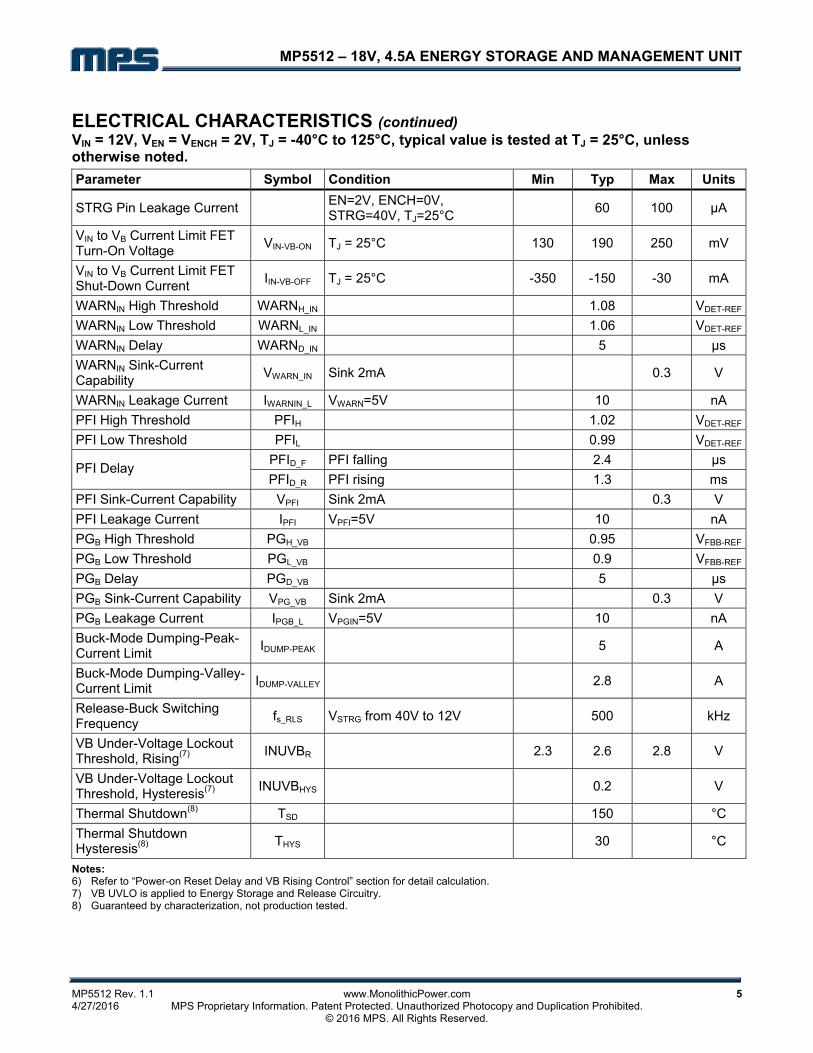
ELECTRICAL CHARACTERISTICS VIN = 12V, VEN = VENCH = 2V, TJ = -40°C to 125°C, typical value is tested at TJ = 25°C, unless otherwise noted.
Parameter Symbol Condition Min Typ Max Units
Input-Supply Voltage Range VIN 4 18 V
Supply Current (Shutdown) IS VEN=0V, TJ = 25°C 3 5 μA
Supply Current (Quiescent) IQ VEN/ENCH=2V, VFBB/FBS/DET=1V 1 2 mA
VCC Regulator VCC Vin or VB=6V, Ivcc=1mA 4.8 5.1 5.5 V
VIN Under-Voltage Lockout Threshold Rising
INUVR 2.5 2.9 3.2 V
VIN Under-Voltage Lockout Threshold Hysteresis
INUVHYS 0.35 V
EN UVLO Threshold Rising ENR 1.2 V
EN UVLO Threshold Falling ENF 0.4 V
VIN to VB Current Limit FET ON Resistance
RDSON 14 mΩ
RILIM=8.25kΩ, TJ = 25°C 1.94 2 2.06 A Continuous-Current Limit ILIM
RILIM=8.25kΩ,TJ = -40°C to 125°C
1.9 2 2.1 A
Current Monitor Output VILIM RILIM=8.25kΩ, IB=2A, TJ = 25°C 1.152 1.2 1.248 V
Off-State Leakage Current ILEAK VIN=12V, VB=0V or VB=12V, VIN=0V, TJ = 25°C
2 4 μA
τR DVDT floating, VIN=12V, test VB rise time
0.9 ms VB Rise Time (dv/dt) Control(6)
IDVDT Connect capacitor to DVDT, test DVDT charge current
1 μA
τD TPOR floating, test reset delay time
0.35 ms Internal RESET Delay-Time Control (6)
ITPOR Connect capacitor to TPOR, test TPOR charge current
1 μA
Pre-Charge Current ICH_PRE 450 mA
Charge Peak Current @ Boost Mode
ICH ICH floating, L=10μH, TJ = 25°C
670 960 1250 mA
Boost-Disconnect Switch Ron Rdison 30 mΩ
Energy Management HS Ron RHon 140 mΩ
Energy Management LS Ron RLon 110 mΩ
TJ = 25°C 0.792 0.8 0.808 V Feedback Voltage
VFBB-REF, VFBS-REF, VDET-REF TJ = -40°C to 125°C 0.784 0.8 0.816 V
Feedback Current IFBB, IFBS,
IDET VFBB=VFBS=VDET=0.8V 10 50 nA
Vs Over-Voltage Threshold VS-OVP 1.1 VFBS-REF
MP5512 – 18V, 4.5A ENERGY STORAGE AND MANAGEMENT UNIT
MP5512 Rev. 1.1 www.MonolithicPower.com 5 4/27/2016 MPS Proprietary Information. Patent Protected. Unauthorized Photocopy and Duplication Prohibited. © 2016 MPS. All Rights Reserved.
ELECTRICAL CHARACTERISTICS (continued) VIN = 12V, VEN = VENCH = 2V, TJ = -40°C to 125°C, typical value is tested at TJ = 25°C, unless otherwise noted.
Parameter Symbol Condition Min Typ Max Units
STRG Pin Leakage Current EN=2V, ENCH=0V, STRG=40V, TJ=25°C
60 100 μA
VIN to VB Current Limit FET Turn-On Voltage
VIN-VB-ON TJ = 25°C 130 190 250 mV
VIN to VB Current Limit FET Shut-Down Current
IIN-VB-OFF TJ = 25°C -350 -150 -30 mA
WARNIN High Threshold WARNH_IN 1.08 VDET-REF
WARNIN Low Threshold WARNL_IN 1.06 VDET-REF
WARNIN Delay WARND_IN 5 μs
WARNIN Sink-Current Capability
VWARN_IN Sink 2mA 0.3 V
WARNIN Leakage Current IWARNIN_L VWARN=5V 10 nA
PFI High Threshold PFIH 1.02 VDET-REF
PFI Low Threshold PFIL 0.99 VDET-REF
PFID_F PFI falling 2.4 μs PFI Delay
PFID_R PFI rising 1.3 ms
PFI Sink-Current Capability VPFI Sink 2mA 0.3 V
PFI Leakage Current IPFI VPFI=5V 10 nA
PGB High Threshold PGH_VB 0.95 VFBB-REF
PGB Low Threshold PGL_VB 0.9 VFBB-REF
PGB Delay PGD_VB 5 μs
PGB Sink-Current Capability VPG_VB Sink 2mA 0.3 V
PGB Leakage Current IPGB_L VPGIN=5V 10 nA
Buck-Mode Dumping-Peak-Current Limit
IDUMP-PEAK 5 A
Buck-Mode Dumping-Valley-Current Limit
IDUMP-VALLEY 2.8 A
Release-Buck Switching Frequency
fs_RLS VSTRG from 40V to 12V 500 kHz
VB Under-Voltage Lockout Threshold, Rising(7)
INUVBR 2.3 2.6 2.8 V
VB Under-Voltage Lockout Threshold, Hysteresis(7)
INUVBHYS 0.2 V
Thermal Shutdown(8) TSD 150 °C
Thermal Shutdown Hysteresis(8)
THYS 30 °C
Notes: 6) Refer to “Power-on Reset Delay and VB Rising Control” section for detail calculation. 7) VB UVLO is applied to Energy Storage and Release Circuitry. 8) Guaranteed by characterization, not production tested.

MP5512 – 18V, 4.5A ENERGY STORAGE AND MANAGEMENT UNIT
MP5512 Rev. 1.1 www.MonolithicPower.com 6 4/27/2016 MPS Proprietary Information. Patent Protected. Unauthorized Photocopy and Duplication Prohibited. © 2016 MPS. All Rights Reserved.
TYPICAL CHARACTERISTICS VIN = 12V, VSTRG = 35V, VPFI = 6.1V, VRLS = 7.8V(9), L = 10µH, POUT = 20W, TA = 25ºC, unless otherwise noted.
SW
ITC
HIN
G F
RE
QU
EN
CY
(kH
z)
EN
UV
LO (
V)
INPUT VOLTAGE (V)
Disabled Supply Current vs. Input Voltage
Vin UVLO Threshold vs. Temperature
Switching Frequency vs. TemperatureVSTRG=24V
Reference Voltage vs. Temperature
EN UVLO Threshold vs. Temperature
TPOR Charge Current vs. Temperature
Buck-Current Limit vs. Temperature
DVDT Charge Current vs. Temperature
QU
IES
CE
NT
CU
RR
EN
T (
mA
)
INPUT VOLTAGE (V)
Quiescent Current vs. Input Voltage
0.0
0.4
0.8
1.2
1.6
2.0
2 4 6 8 10 12 14 16 18 200.0
1.0
2.0
3.0
4.0
5.0
2 4 6 8 10 12 14 16 18 201.0
1.5
2.0
2.5
3.0
3.5
4.0
-50 -25 0 25 50 75 100125150
VIN
UV
LO (
V)
VIN UVLO Rising
VIN UVLO Falling
0.0
0.2
0.4
0.6
0.8
1.0
1.2
1.4
-50 -25 0 25 50 75 100 125 150
EN UVLO Rising
EN UVLO Falling
0
100
200
300
400
500
600
700
-50 -25 0 25 50 75 100 125 150740
760
780
800
820
840
860
-50 -25 0 25 50 75 100 125 150
RE
FE
RE
NC
Y V
OLT
AG
E (
mV
)
0.0
0.5
1.0
1.5
2.0
-50 -25 0 25 50 75 100 125 1500.0
0.5
1.0
1.5
2.0
-50 -25 0 25 50 75 100 125 1500.0
1.0
2.0
3.0
4.0
5.0
6.0
-50 -25 0 25 50 75 100 125 150
BU
CK
CU
RR
EN
T L
IMIT
(A
)
Peak Curretn Limit
Valley Current Limit
FB B
FB S
DET

MP5512 – 18V, 4.5A ENERGY STORAGE AND MANAGEMENT UNIT
MP5512 Rev. 1.1 www.MonolithicPower.com 7 4/27/2016 MPS Proprietary Information. Patent Protected. Unauthorized Photocopy and Duplication Prohibited. © 2016 MPS. All Rights Reserved.
TYPICAL CHARACTERISTICS (continued) VIN = 12V, VSTRG = 35V, VPFI = 6.1V, VRLS = 7.8V(9), L = 10µH, POUT = 20W, TA = 25ºC, unless otherwise noted.
200
220
240
260
280
300
320
340
0.0
0.5
1.0
1.5
2.0
2.5
0 50 100 150 200 250 3000.0
0.2
0.4
0.6
0.8
1.0
1.2
1.4
0 0.4 0.8 1.2 1.6 2 2.4
-50 -25 0 25 50 75 100 125 1500
1
2
3
4
5
6
2 4 6 8 10 12 14 16 18 200
10
20
30
40
50
0 10 20 30 40 50
CU
RR
EN
T L
IMIT
(A
)
CU
RR
EN
T L
IMIT
(A
)
VIN to VB Current Limit vs. ILIM Resistor
Boost-Charge Peak Current vs. ICH Resistor
VB Rising Time vs. DVDT Capacitance
-50 -25 0 25 50 75 100 125 150
DVDT CAPACITANCE (nF)
VB
RIS
E T
IME
(m
S)
VIN=12V
VIN=5V
INPUT CURRENT (A)
ILIM
PIN
VO
LTA
GE
(V
)
BO
OS
T P
EA
K C
UR
RE
NT
(A
)
BO
OS
T P
EA
K C
UR
RE
NT
(m
A)
1.8
1.9
2.0
2.1
2.2
Boost Pre-charge Current vs. Temperature
PR
E-C
HA
RG
E C
UR
RE
NT
(m
A)
300
350
400
450
500
550
600
-50 -25 0 25 50 75 100 125 150
Notes:
9) VRLS voltage varies a little with different VSTRG voltage because the internal RAMP voltage on FBB changes with duty cycle. 7.8V voltage is estimated based on 30V VSTRG condition.

MP5512 – 18V, 4.5A ENERGY STORAGE AND MANAGEMENT UNIT
MP5512 Rev. 1.1 www.MonolithicPower.com 8 4/27/2016 MPS Proprietary Information. Patent Protected. Unauthorized Photocopy and Duplication Prohibited. © 2016 MPS. All Rights Reserved.
TYPICAL PERFORMANCE CHARACTERISTICS VIN = 12V, VSTRG = 35V, VPFI = 6.1V, VRLS = 7.8V(9), L = 10µH, TA = 25ºC, POUT = 20W, unless otherwise noted.
0
30
60
90
120
150
180
0 500 1000 1500 2000 25000 1 2 3 4 510
15
20
25
30
35
40
45
0 0.1 0.2 0.3 0.4 0.5 0.6
Backup-Release EfficiencyVB_RLS=5V
Storage-Charge Voltage vs. Charge Time RICH=Float
CHARGE TIME (s)
ST
OR
AG
E V
OLT
AG
E (
V)
10
15
20
25
30
35
40
45
CHARGE TIME (s)
ST
OR
AG
E V
OLT
AG
E (
V)
Release Timevs. Storage Capacitance
RE
LEA
SE
TIM
E (
ms)
IB_load=1A
IB_load=3A
STORAGE VOLTAGE (V)
70
75
80
85
90
95
100
5 10 15 20 25 30 35 40
IB=1A
IB=2AIB=3A
Backup-Release EfficiencyVB_RLS=7.8V
STORAGE VOLTAGE (V)
70
75
80
85
90
95
100
5 10 15 20 25 30 35 40
IB=1A
IB=2AIB=3A
Backup-Release EfficiencyVB_RLS=10V
STORAGE VOLTAGE (V)
70
75
80
85
90
95
100
5 10 15 20 25 30 35 40
IB=1A
IB=2AIB=3A

MP5512 – 18V, 4.5A ENERGY STORAGE AND MANAGEMENT UNIT
MP5512 Rev. 1.1 www.MonolithicPower.com 9 4/27/2016 MPS Proprietary Information. Patent Protected. Unauthorized Photocopy and Duplication Prohibited. © 2016 MPS. All Rights Reserved.
TYPICAL PERFORMANCE CHARACTERISTICS (continued) VIN = 12V, VSTRG = 35V, VPFI = 6.1V, VRLS = 7.8V(9), L = 10µH, TA = 25ºC, POUT = 20W, unless otherwise noted.

MP5512 – 18V, 4.5A ENERGY STORAGE AND MANAGEMENT UNIT
MP5512 Rev. 1.1 www.MonolithicPower.com 10 4/27/2016 MPS Proprietary Information. Patent Protected. Unauthorized Photocopy and Duplication Prohibited. © 2016 MPS. All Rights Reserved.
PIN FUNCTIONS QFN28
(4mm×5mm) Pin #
Name Description
1 CST Storage Capacitor for Internal Charge Pump. Requires 10nF decouple capacitor between CST and AGND to drive the MOSFET current limit. Do not connect to a capacitor with over 47nF.
2 VCC Internal LDO Output. VCC provides power for internal circuits. Decouple with a 1µF ceramic capacitor. Connect the capacitor as close to VCC as possible.
3 ILIM DC Input Current Limit. Connect a resistor between ILIM and AGND to adjust the DC limit from VIN to VB.
4 TPOR Power-On-Reset Delay. Connect a capacitor between TPOR and AGND to determine the power-on-reset delay time. During the default power-on-reset delay time, leave TPOR floating for 0.35ms.
5 DVDT Bus Voltage Start-Up Slew Rate. Connect a capacitor from DVDT to AGND. Leave it floating for the default soft-start time (around 0.9ms from 0V to 12V).
6 PFI
Power-Failure Indicator. PFI is an open-drain output. To indicate a signal, PFIshould be pulled up to a power source through a resistor. PFI goes high if the DETvoltage exceeds 1.02×VDET-REF. PFI goes low if the DET voltage drops below 0.99×VDET-REF. If MP5512 is disabled by UVLO or EN UVLO, it operates with high impedance.
7 WARN
VIN Voltage-Drop Warning Indicator. WARN is an open-drain output. To indicate a signal, WARN should be pulled up to a power source through a resistor. WARNgoes high if the DET voltage exceeds 1.08×VDET-REF. WARN goes low if the DETvoltage drops below 1.06×VDET-REF. WARN indicates the input power distance to theset supply-voltage level. If MP5512 is disabled by UVLO or EN UVLO, it operates with high impedance.
8 PGB
Bus Voltage Power-Good Indicator. PGB is an open-drain output. To indicate a signal, PGB should be pulled up to a power source through a resistor. PGB goes high if the FBB voltage exceeds 0.95×VFBB-REF. PGB goes low if the FBB voltage drops below 0.9×VFBB-REF. If MP5512 is disabled by UVLO or EN UVLO, it operates with high impedance.
9 AGND IC Signal Ground.
10 DET Input-Voltage Detection Sense. DET sets the buck-release start voltage when VIN
drops.
11, 28 VIN
Input-Supply Voltage. The MP5512 operates from an unregulated 4V-to-18V input. Place a 0.1µF ceramic capacitor as close to VIN as possible. A TVS diode at input is necessary if the VIN voltage spike is high. Refer to the “Selecting Input Capacitor and TVS” sections.
12, 27 VB Bus Voltage. VB requires a 22μF-to-47μF ceramic capacitor as close to VB as possible.
13 EN ON/OFF Control. EN enables/disables all internal circuits.
14 VBO Source of Internal Isolation MOSFET. Connect the inductor between SW and VBOfor boost and buck operation.
15 ENCH Boost Converter ON/OFF Control. ENCH enables/disables the energy-storage function but does not limit the release function.
16 ICH Boost-Mode Charge Switching-Peak Current Adjustment.

MP5512 – 18V, 4.5A ENERGY STORAGE AND MANAGEMENT UNIT
MP5512 Rev. 1.1 www.MonolithicPower.com 11 4/27/2016 MPS Proprietary Information. Patent Protected. Unauthorized Photocopy and Duplication Prohibited. © 2016 MPS. All Rights Reserved.
PIN FUNCTIONS (continued)
QFN28 (4mm×5mm)
Pin # Name Description
17 FBB Bus-Voltage Feedback Sense. FBB Regulates the bus voltage in buck mode.
18 FBS Storage-Voltage Feedback Sense. FBS sets the storage voltage in boost mode.
19 RTEST
STRG residual energy discharge resistor connection pin in evaluation test. When Vin/VB or EN powers off, RTEST is pulled to PGND internally. One external resistor from RTEST to STRG discharges STRG voltage for a residual energy discharge. The discharge current must be lower than 500mA. This discharge resistor can avoid any spark if we touch STRG after IC disabled in evaluation test.
20 BST Bootstrap. Requires the bootstrap capacitor from BST to SW to supply the high-side switch driver.
21,22,23,24 STRG Storage. Connect the storage capacitor for energy storage and release circuitry.
25 SW Switch output. For energy storage and release circuitry, connect a small inductor between SW and VBO.
26 PGND Power Ground.

MP5512 – 18V, 4.5A ENERGY STORAGE AND MANAGEMENT UNIT
MP5512 Rev. 1.1 www.MonolithicPower.com 12 4/27/2016 MPS Proprietary Information. Patent Protected. Unauthorized Photocopy and Duplication Prohibited. © 2016 MPS. All Rights Reserved.
FUNCTION DIAGRAM
HS Drive
LS Drive
Control for Current Limit & Energy Management Circuit
VIN
PGB
DVDT
TPORILIM
ICH
FBB
VB VBO SW BST
STRG
FBS
PGNDFBS
EN
WARN
DET
5V LDOVCC
ENCH
PFI
Charge PumpCST
RTEST
AGND
To DC Converter
FBB
Figure 1: Functional Block Diagram

MP5512 – 18V, 4.5A ENERGY STORAGE AND MANAGEMENT UNIT
MP5512 Rev. 1.1 www.MonolithicPower.com 13 4/27/2016 MPS Proprietary Information. Patent Protected. Unauthorized Photocopy and Duplication Prohibited. © 2016 MPS. All Rights Reserved.
OPERATION The MP5512 is an energy storage and management unit in a 4mm×5mm 28-pin QFN package. It provides a compact and efficient energy management solution for typical solid-state–drive or hard-disk drive applications. MPS’ patented lossless-energy storage and release-management circuits use a bi-directional buck/boost converter to achieve optimal energy transfer and provide a cost-effective energy-storage solution.
MP5512’s built-in boost-mode converter charges the storage bulk capacitor to a programmed voltage when the system is powered up. In case of an input power failure, MP5512 flags the power failure, disconnects the input power and transfers the energy from the storage capacitor to the bus capacitor via the built-in buck mode converter. This supports SSD system data backup. The buck converter works in 100% duty-cycle operation to fully deplete the stored energy.
Start-Up When the VIN power and enable signal are higher than their UVLO, MP5512 starts up with the programmed power-on-reset delay time. Initially, the hot-swap MOSFET from VIN to VB is on and the bus capacitor is charged from 0 to VIN under dv/dt control.
VINEN=ENCH
Storage-Voltage
Power-On-Reset Delay Time
Target storage voltage
BUS Voltage
Charge Up VB with dv/dt Control
Boost for Storage
DVDT
VPFI
Boost-Delay Time
Pre-Charge
Figure 2: Charging Process
When DET voltage is higher than 1.02×VDET-REF, PFI is set to high to indicate the power condition. If PFI is high and dv/dt voltage is saturated, the charge circuit is enabled to charge storage
capacitors on STRG (after about 1.8ms delay time). The storage voltage is charged with 450mA trickle current during the pre-charge period. Once the storage voltage is close to VB voltage, the boost-switching circuit initiates and the storage voltage is boosted to the target voltage (see Figure 2).
Storage Voltage
After the start-up period, the internal boost converter automatically regulates the storage voltage to the set value. The MP5512 uses burst mode to minimize the converter’s power loss. When the storage voltage drops below the set voltage, burst mode initiates and charges the storage capacitor. During the burst period, the current limit and the low-side MOSFET control the boost. When the power MOSFET turns on, the inductor current increases until it reaches its current limit. After hitting the current limit, the power MOSFET turns off for the set minimum off time. If the feedback voltage remains below the 0.8V internal reference at the end of the minimum off time, the power MOSFET turns on again. Otherwise, the MP5512 waits until the voltage drops below the reference threshold before turning on. In boost mode, the high-side MOSFET won’t turn on and the inductor current conducts through the body-diode of HS-FET.
The boost-current limit is programmed by the ICH resistor. The programmed boost-switching current limit can be estimated with:
710)(
35)(
L
V
kRAI IN
ICHCH
Where RICH is the resistor connected to the ICH and L is the boost inductor.
If the ICH is floating, the boost-peak current limit is about 960mA (for typical 12V input and 10uH inductor applications).
MP5512 has over-voltage protection for STRG voltage. If the feedback voltage of VSTRG on FBS is over 1.1 x VFBS-REF, MP5512 shuts down the low-side MOSFET

MP5512 – 18V, 4.5A ENERGY STORAGE AND MANAGEMENT UNIT
MP5512 Rev. 1.1 www.MonolithicPower.com 14 4/27/2016 MPS Proprietary Information. Patent Protected. Unauthorized Photocopy and Duplication Prohibited. © 2016 MPS. All Rights Reserved.
in both boost and buck mode until VSTRG drops to the regulated voltage.
Release
Once the input power drops, and DET voltage is lower than 1.06×VDET-REF, WARN gives out a warning signal to indicate the input drop condition. Once DET drops to 0.99×VDET-REF the internal boost converter stops charging and works in buck-release mode. Simultaneously, the hot-swap MOSFET shuts down to prevent a negative current from VB to VIN.
In buck mode, the part transfers energy from the high-voltage storage capacitor to the low-voltage bus capacitor. The regulated bus voltage is determined by VFBB-REF and the resistor divider from VB to FBB.
The released buck adopts a fixed-frequency constant-on-time (COT) mode. The buck converter works until the storage-capacitor voltage approaches the bus voltage. The storage and bus voltages drop simultaneously until they reach the downstream DC-DC converter’s UVLO or VB_UVLO (see Figure 3).
Figure 3: Release Times
The buck mode has a peak-current limit function to limit the release current; the released-peak current is about 5A. If an inductor current triggers the current limit, the high-side switch won’t turn on until the inductor current drops to a valley-current limit. The buck converter works in pulse-skip mode at light load to save the switching-power loss.
Input Recovery Start-up
If the input power fails and comes back before VB drops to UVLO, the storage capacitor re-charges. In this condition, PFI switches to high, and the hot-swap MOSFET turns on (if VIN is 190mV higher than VB). Following a 1.8ms delay (after DVDT saturation), the buck function turns off and boost function is re-enabled to regulate the storage capacitor at VSTRG voltage. See Figure 4 for the re-charge sequence. If PFI goes high but VIN is still lower than VB, the hot-swap MOSFET cannot turn on. The buck regulator slightly decreases the regulated VB voltage so the hot-swap MOSFET can turn on again.
If VB drops lower than UVLO before VIN returns, MP5512 begins a new startup sequence as the VIN rises.
VIN
Hot-Swap
Storage Voltage
PFI=1 and VIN > VB +0.19V
BUS Voltage
Re-Boost Up
DVDT
VPFI
Charge Up VB with dv/dt Control
Buck Mode withNo Switching
Release
DelayPFI
Delay
Figure 4: Re-Charge Sequence
Input-Current Limit
The input-current limit controls the inrush current of the internal hot-swap MOSFET at startup. A capacitor connected to DVDT sets the soft-start time. In addition to soft-start, the ILIM limits the steady-state current by connecting a resistor between ILIM and AGND. The current limit can be estimated from:

MP5512 – 18V, 4.5A ENERGY STORAGE AND MANAGEMENT UNIT
MP5512 Rev. 1.1 www.MonolithicPower.com 15 4/27/2016 MPS Proprietary Information. Patent Protected. Unauthorized Photocopy and Duplication Prohibited. © 2016 MPS. All Rights Reserved.
ILIMILIM
17.2I (A) 0.085
R (k )
Where, RILIM is the current-limit setting resistor from ILIM to GND.
The voltage on ILIM monitors and indicates the current in the hot-swap MOSFET. The relationship between the input current and ILIM voltage can be estimated by:
IN ILIMILIM ILIM
I (A) R (k )V (V) 0.0085 R (k )
14.6
Reverse-Current Protection
The Vin-to-VB hot-swapping MOSFET turns on when input voltage exceeds the VIN UVLO threshold (during initial start up). It turns off when DET voltage falls, causing the MP5512 to enter buck-release mode. It turns on again if VIN > VB + 0.19V.
The hot-swapping circuit applies reverse-current protection when energy is released from the storage capacitors to VB. Typically 150mA reverse current from VB to VIN shuts down the hot-swap MOSFET.
Power-On Reset Delay and VB Rising Control
TPOR controls the power-on-reset function for hot-swapping. By floating TPOR, the TPOR time is about 0.35ms. If an external capacitor is connected to TPOR, an internal 1μA current charges the capacitor and determines the TPOR time (with 0V-to-1V TPOR capacitor charge time). The power-reset-delay time can be estimated as:
A
VCT TPOR
D
1
1
After TPOR time, one capacitor across the DVDT programs VB soft-start time. During the SS period, the relationship between VB and DVDT voltage can be estimated by:
DVDTVB 15.4 V
Where, VDVDT is DVDT capacitor voltage charged by 1μA current (eventually VDVDT is charged saturated to about 1.23V).
The VB soft-start time from 0V to VIN can be estimated by:
A
CVBT DVDT
R
14.15
By floating DVDT, the VB rising time from 0V to 12V is typically 0.9ms.
Start-Up Sequencing
After the IC is enabled, MP5512 starts to work with the TPOR reset time and DVDT soft-start time. During VB rising time, an internal charge pump charges the CST capacitor. This provides the driver source for the hot-swap MOSFET. Too short of a DVDT time may trigger the input current-limit threshold. Too large of a CST capacitor may affect the charge-pump slew rate. A 10nF CST capacitor is recommended. During DVDT soft-start, the VB capacitor is charged; the STRG capacitor is not charged.
Once VB is charged, DVDT voltage charges to about 1.23V and holds at this saturated voltage. If PFI is high and DVDT saturates, the charge function is enabled and the storage capacitor charges to target voltage.
VCC Power Management
MP5512 internal circuits are powered from the Vcc capacitor, which is regulated by VIN in normal conditions. In case of VIN failure, a Vcc power source is supplied by the VB source allowing the buck converter to continue to work. A capacitor with no less than 1uF is required to VCC.
Enable Control
The MP5512 EN and ENCH have different functions. EN enables/disables all internal circuits, and ENCH only controls the boost- charge of the storage voltage. When ENCH is high, boost functions and storage voltage are regulated. Once ENCH is pulled low, the boost mode stops and storage voltage discharges from the leakage current. The ENCH signal cannot control buck mode. The buck converter continues to work if input power fails, even when ENCH is low. Normally, EN must be pulled up to both Vin and VB, and ENCH must be pulled up to VB or VCC.

MP5512 – 18V, 4.5A ENERGY STORAGE AND MANAGEMENT UNIT
MP5512 Rev. 1.1 www.MonolithicPower.com 16 4/27/2016 MPS Proprietary Information. Patent Protected. Unauthorized Photocopy and Duplication Prohibited. © 2016 MPS. All Rights Reserved.
EN and ENCH cannot be connected to voltage higher than 6.5V. For a resistor pull-up condition, an internal zener diode clamps the voltage at EN/ENCH. The maximum pull-up current for the internal zener clamp (assuming the worst case with 6V) should be less than 0.2mA. Pulled up to Vin and VB, a typical 100kΩ pull-up resistor is recommended.
Bus Voltage Power-Good Indicator ( PGB)
When the voltage on the FBB (VB feedback) drops below 0.9×VFBB-REF, the MP5512 internally pulls the PGB low. When the FBB voltage is above 0.95×VFBB-REF, it goes high (if externally pulled up by a resistor).
Input-Power Warning and Power-Failure Indicator (PFI)
When the voltage on the DET (VIN feedback) rises to 1.08×VDET-REF, WARN goes high (if externally pulled up by a resistor). It pulls low if DET voltage drops to 1.06×VDET-REF. There is a warning signal for the next power stage by informing the VIN drop portent.
If DET drops below 0.99×VDET-REF, the MP5512 internally pulls the PFI low. This signals the DET to leave boost mode. If DET voltage rises to 1.02xVDET-REF, PFI sets to high again (if externally pulled up by a resistor).
Residual Storage-Energy Discharge
In buck release mode, MP5512 discharges the storage voltage to VB_UVLO, but the residual voltage holds for a longer time period due to the large storage capacitance. The residual voltage is worse if MP5512 is disabled by the EN signal.
When MP5512 is disabled, RTEST is pulled to PGND internally, an external resistor from VSTRG to RTEST helps to discharge the residual energy. The RTEST is self-driven and storage voltage is discharged to about 0.8V, even if MP5512 input is not available. Choose an efficient, external discharge resistor to limit the maximum RTEST current to lower than 500mA.
Thermal Shut Down (TSD)
Thermal shutdown is implemented to prevent the chip from thermal damage. When the silicon die temperature is higher than its upper threshold, it shuts down the chip. When the temperature is lower than its lower threshold, the chip is enabled again with a new start-cycle.

MP5512 – 18V, 4.5A ENERGY STORAGE AND MANAGEMENT UNIT
MP5512 Rev. 1.1 www.MonolithicPower.com 17 4/27/2016 MPS Proprietary Information. Patent Protected. Unauthorized Photocopy and Duplication Prohibited. © 2016 MPS. All Rights Reserved.
APPLICATION INFORMATION Setting the Storage Voltage
Set the storage voltage by choosing the external feedback resistors R5 and R6 (see Figure 5)..
Figure 5: Storage Feedback Circuit
The storage voltage is determined by:
STORAGE FBS REF
R5V (1 ) V
R6
Where, VFBS-REF is 0.8V typically. R5 and R6 are not critical for normal operation. Select an R6 resistor higher than 10kΩ to reduce the bleed current and lower than 50kΩ to enhance noise immunity. For example, if R6 is 10kΩ, R5 is calculated as:
REFFBS
REFFBSSTORAGE
V
VVkR
)(105
For a 24V storage voltage, R5 is 290kΩ.
Table 1 lists the recommended feedback resistance for different storage voltages.
Table 1: Resistor Pairs for VSTORAGE
VSTORAGE(V) R5 (kΩ) R6 (kΩ) 12 140 10 24 290 10 40 490 10
Setting VIN Power-Failure Threshold Voltage and VB Release-Regulation Voltage
Set the release-trigger voltage by choosing the external feedback resistors R1 and R2 (see Figure 6). Release-trigger voltage is determined by 0.99xVDET-REF, which is 0.792V.
The input power-failure release threshold is:
VR
RVPFI 792.0)
2
11(
R1
R2
VIN
DETC1
Figure 6: Release-Feedback Circuit VDET determines the release-trigger voltage and VFBB determines VB release-regulation voltage (see Figure 7).
R3
R4
VB
FBBC2
Figure 7: VB Regulation Feedback Circuit
The bus-regulation voltage can be calculated by:
)2
()4
31( RAMP
REFFBBRLS
VV
R
RVB
Where, VRAMP is buck FBB internal compensation ramp voltage, and can be estimated as:
)220
10)1(
6
SWSTRGRAMP F
DDVV
Where, VFBS-REF is 0.8V typically. D is the buck duty cycle, and FSW is the switching frequency.
R3 and R4 are related to buck-release stability. Since the release-buck mode works in COT mode, try to avoid small resistor values that affect the internal voltage ramp. Generally, choose R3//R4≥10kΩ for stable performance with CB=22μF.
Selecting the Storage Capacitor
The storage capacitor stores energy during normal operation and releases this energy to VB when VIN loses input power. Use a general-
MP5512 – 18V, 4.5A ENERGY STORAGE AND MANAGEMENT UNIT
MP5512 Rev. 1.1 www.MonolithicPower.com 18 4/27/2016 MPS Proprietary Information. Patent Protected. Unauthorized Photocopy and Duplication Prohibited. © 2016 MPS. All Rights Reserved.
purpose electrolytic capacitor or low-profile POS capacitor for most applications. Select a storage capacitor with a voltage margin 20% higher than the targeted storage voltage. When choosing the capacitors, consider the capacitance reduction with the DC voltage offset. Different capacitors have different capacitance de-rating performances. Choose a capacitor with a voltage rating high enough to guarantee enough capacitance.
The required capacitance depends on the length of the “dying gasp” for a typical application. Assume the bus-release current is IRELEASE when bus voltage is regulated at VBRLS for the DC-DC converter. The storage is VSTRG, and the required dying gasp time is τDASP. The required storage capacitance is:
EffVBV
IVBC
RLSGSTR
DASPRELEASERLSSTRG
)(
222
Eff is the energy-release efficiency in the buck converter, which can run up to 90% efficiency in most applications. Select the proper storage capacitance to ensure enough capacitance for buck-power loss. If IRELEASE=1A, τDASP=20ms, VSTORAGE=24V, and VBRLS-=10V, then the required storage capacitance is 1000μF.
Setting the Input Hot-Swap Current Limit Connect a resistor from ILIM to AGND to set the current-limit value. For example, a 8.25kΩ resistor sets the current limit to about 2A. Refer to the “Input-Current Limit” section for current-limit calculation. Table 2 lists recommended resistors for different current-limit values.
Table 2: ILIM vs. RILIM
ILIM(A) RLIM (kΩ) 4.5 3.74 3.54 4.75
2 8.25
Setting the Boost Peak-Current Limit
Connect a resistor from ICH to AGND to set the boost peak-inductor current. Refer to the “Storage Voltage” section for boost-peak current-limit setting calculation. If ICH is floating, the boost
peak-current limit is about 960mA ( in typical 12V input and 10μH inductor conditions).
Selecting the Inductor
The inductor is necessary to supply constant current to the load. Since the boost mode and buck mode share the same inductor (and generally buck-mode current is higher), the inductor supporting the buck-mode releasing current is recommended.
Select the inductor based on the buck-releasing mode. If the storage voltage is VSTRG, the bus-regulation voltage is VBRLS, with the buck running at a fixed 500kHz frequency. The inductance value can be calculated by:
)1(STRG
RLS
SWL
RLS
V
VB
FI
VBL
Where ΔIL is the peak-to-peak inductor-ripple current, which can be set at 30% to 40% of the full-releasing current.
The inductor should not saturate under the maximum inductor-peak current.
Setting the Power-On-Reset Delay Time
Connect a capacitor to the TPOR to set the power–on-reset delay time. Leave it floating for the default delay time of around 0.35ms. Table 3 lists the recommended capacitors for different delay times.
Table 3: Reset Delay vs. Capacitor Value
τD (ms) CTPOR (nF) 100 100 500 500
Setting the Bus Voltage Rise Time
Connect a capacitor to the DVDT to set the bus voltage start-up slew rate and soft-start time. Leave it floating for the default soft-start time (around 0.9ms from 0V to 12V). Table 4 lists the recommended capacitors for different soft-start times for a 12V input condition. It has a proportional VB soft-start time in other input voltage conditions.

MP5512 – 18V, 4.5A ENERGY STORAGE AND MANAGEMENT UNIT
MP5512 Rev. 1.1 www.MonolithicPower.com 19 4/27/2016 MPS Proprietary Information. Patent Protected. Unauthorized Photocopy and Duplication Prohibited. © 2016 MPS. All Rights Reserved.
Table 4: Soft-Start vs. Capacitor Value when VIN=12V
τR (ms) Cdv/dt (nF) 7.8 10 78 100
Selecting BST and CST Capacitance
The BST capacitor supplies power to the buck converter high-side MOSFET. A 0.1uF~1uF ceramic capacitor is recommended for BST decoupling. The CST capacitor supplies power for the input hot-swap MOSFET and the STRG disconnecting MOSFET. The CST capacitor also supplies power to BST when the buck is working in a 100% duty cycle. The CST capacitor is charged by an internal charge pump; a 10nF ceramic capacitor is recommended. A CST capacitor with more than 47nF capacitance is not recommended as it affects the voltage charge-up slew rate.
Selecting Input Capacitor and TVS
Capacitors at VIN are recommended to absorb possible voltage spikes during input-power turn on, input-switch hard off (during power off), or other special conditions. The application determines the capacitor. For example, if the input power trace is too long (with higher parasitic inductance), during the input-switch hard off period, more energy pumps into the input. This means more input capacitors are needed for the input voltage spike to stay in a safe range. Use a 0.1uF or larger capacitor.
Keep inrush-current requirements in mind when selecting an input capacitor. Typically, more input capacitors result in a higher input-inrush current during hot-plugging. A smaller input capacitor is needed for a smaller inrush current. MP5512 works normally with a very small input capacitor. It works without an input capacitor as well. However, this leads to a possible high-voltage spike. An efficient solution is to add a TVS diode at the input to absorb the possible input-voltage spike. At the same time, keep the inrush current small during hot-plugging. A typical TVS diode, like SMA6J13A is recommended.
Selecting the External Diode
For release-mode, one schottky diode between SW and PGND is recommended. This diode
conducts a low-side current during switching dead-time or a high-switching current condition. Small package diodes such as DFLS260 or SBR3U60P1 are recommended due to their small package size, low voltage drop and high-power capabilities.
For charge mode, the internal high-side MOSFET is not turned on and current is conducted through the MOSFET body-diode. One schottky diode between SW and STRG is recommended since the boost-peak current can reach up to 2A. The diode-voltage rating should be higher than the storage voltage. The current rating should be higher than the diode current programmed by ICH. Small package diodes such as DFLS260 or SBR3U60P1 are recommended. This diode is not necessary if the boost peak-current limit is as low as 0.5A.
Layout Recommendation
1) The high-current paths (VIN, VB, VBO, SW, STRG, and PGND) should use short, wide and direct traces.
2) While VBO is far from SW, keep the SW trace as short as possible.
3) Put the decoupling capacitor across VB and PGND (as close as possible).
4) Put the schottky diode D1 across SW and PGND as close to the IC as possible.
5) Put the decoupling capacitor across STRG and PGND (as close as possible). When using a large volume capacitor, a small size 1uF ceramic capacitor is required. Place it as close to STRG and PGND as possible.
6) Put the decoupling capacitor across Vcc and AGND (as close as possible).
7) Keep the switching node SW short and away from the feedback network.
MP5512 – 18V, 4.5A ENERGY STORAGE AND MANAGEMENT UNIT
MP5512 Rev. 1.1 www.MonolithicPower.com 20 4/27/2016 MPS Proprietary Information. Patent Protected. Unauthorized Photocopy and Duplication Prohibited. © 2016 MPS. All Rights Reserved.
8) The external feedback resistors should be placed next to FBB/FBS/DET.
9) Keep the BST voltage path (BST, C5 and SW) as short as possible.
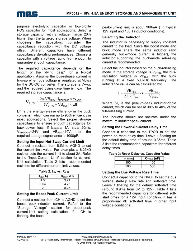
10) All signal grounds should be connected together and then connected to PGND with a one-point connection.
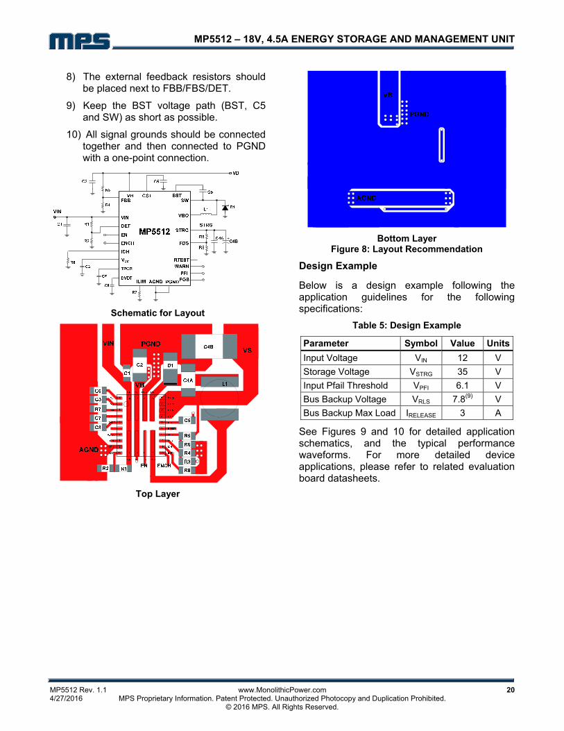
Schematic for Layout
Top Layer
Bottom Layer Figure 8: Layout Recommendation
Design Example
Below is a design example following the application guidelines for the following specifications:
Table 5: Design Example
Parameter Symbol Value Units
Input Voltage VIN 12 V
Storage Voltage VSTRG 35 V
Input Pfail Threshold VPFI 6.1 V
Bus Backup Voltage VRLS 7.8(9) V
Bus Backup Max Load IRELEASE 3 A
See Figures 9 and 10 for detailed application schematics, and the typical performance waveforms. For more detailed device applications, please refer to related evaluation board datasheets.

MP5512 – 18V, 4.5A ENERGY STORAGE AND MANAGEMENT UNIT
MP5512 Rev. 1.1 www.MonolithicPower.com 21 4/27/2016 MPS Proprietary Information. Patent Protected. Unauthorized Photocopy and Duplication Prohibited. © 2016 MPS. All Rights Reserved.
TYPICAL APPLICATION CIRCUITS
SW
VBO
STRG
FBS
RTEST
WARN
PFI
PGBDVDT
TPOR
VCC
ENCH
EN
DET MP5512
VIN
U1
169kR3
22uFC2B
20kR4
AGND
PGND
10nFC6
AGND
1uFC5
10uHL1
430kR5
10kR6
AGND
4.75kR7
AGND PGND
NSC8
AGND
NSC7
AGND
1uFC3
AGND
200kR8
100kR1
15kR2
0.1uFC1
PGND
AGND
NSR9
1uFC4A
PGND
100kR14
100kR13
100kR12100kR11100kR10
1000uFC4B
PGND
VCC
100kR15
0.1uFC2A
PGNDD1DFLS240
D3NS
PGND
D2NS
VCC
VIN
VB
VS
Figure 9: 12V Input, 35V Storage Typical Application Circuit
Figure 10: 5V Input, 12V Storage Typical Application Circuit

MP5512 – 18V, 4.5A ENERGY STORAGE AND MANAGEMENT UNIT
NOTICE: The information in this document is subject to change without notice. Please contact MPS for current specifications. Users should warrant and guarantee that third party Intellectual Property rights are not infringed upon when integrating MPS products into any application. MPS will not assume any legal responsibility for any said applications.
MP5512 Rev. 1.1 www.MonolithicPower.com 22 4/27/2016 MPS Proprietary Information. Patent Protected. Unauthorized Photocopy and Duplication Prohibited. © 2016 MPS. All Rights Reserved.
PACKAGE INFORMATION
QFN-28 (4mmX5mm)

Mouser Electronics
Authorized Distributor
Click to View Pricing, Inventory, Delivery & Lifecycle Information: Monolithic Power Systems (MPS):
MP5512GV-P