Embed Size (px)
Citation preview

Moving to leading-edge technology nodes
Federico Faccio CERN EP-ESE-ME
(seriously?)
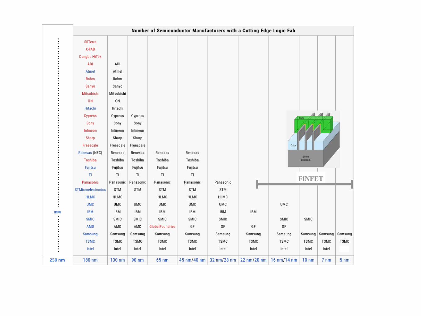
250nm
IBM
FINFET
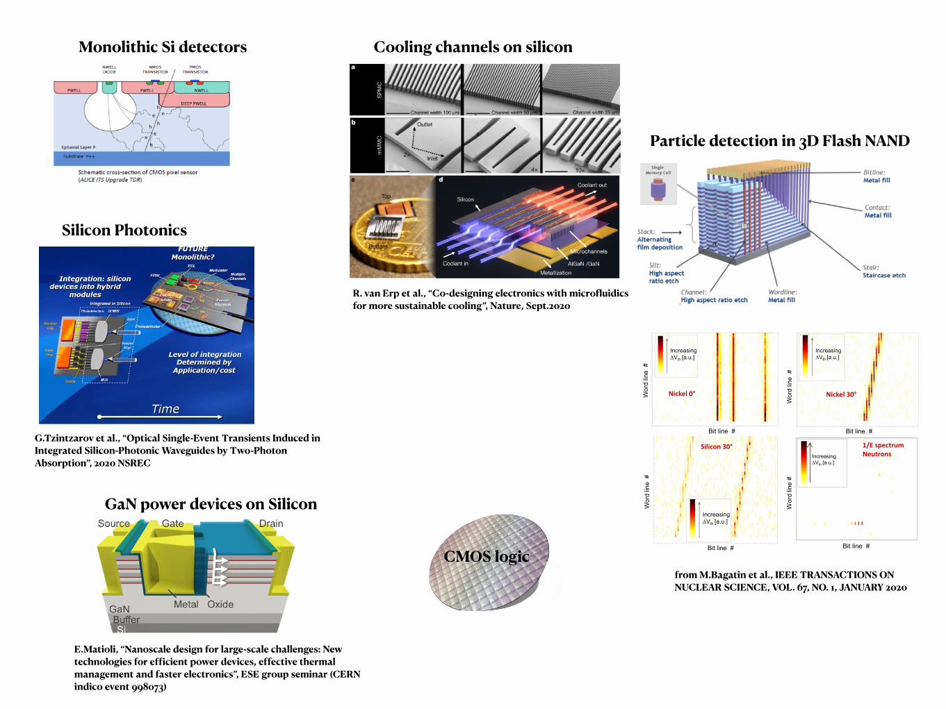
Monolithic Si detectors
G.Tzintzarov et al., “Optical Single-Event Transients Induced in Integrated Silicon-Photonic Waveguides by Two-Photon Absorption”, 2020 NSREC
Silicon Photonics
GaN power devices on Silicon
E.Matioli, “Nanoscale design for large-scale challenges: New technologies for efficient power devices, effective thermal management and faster electronics”, ESE group seminar (CERN indico event 998073)
R. van Erp et al., “Co-designing electronics with microfluidics for more sustainable cooling”, Nature, Sept.2020
Cooling channels on silicon
In this paper, we expand the work presented in [13], showing a fully working implementation of the 3D based SEU monitor, and propose new and complete algorithms for the extraction of the beam parameters, based only on user-mode commands (i.e. those available to the users and documented in the memory datasheet). A new experimental validation will be presented, using LETs much lower than those used in [13], in order to stress the capabilities of the 3D NAND Flash radiation monitor, in terms of particle fluence, angle of incidence, and LET of impinging particles. Extraction of the threshold voltage shifts induced by different low LETs will be shown using only user-mode routines, and compared with results obtained with reserved test-mode routines provided by the manufacturer. Although some parameters need to be still fully optimized and calibrated, the efficacy of the proposed solution appears to be remarkable.
The paper is organized as follows: section II illustrates the hardware and software architecture and is split in several subsections dealing with hardware, stored pattern, radiation-induced errors, measurement of fluence, angle of incidence, uniformity, LET; section III presents the experimental validation at GSI facility. Conclusions are finally drawn on the benefits and shortcomings of the proposed SEU monitor.
II. HARDWARE AND SOFTWARE ARCHITECTURE AND OPERATIONS
A. Overview and main components
The radiation monitor prototype shown in Fig. 2 consists of: a) a hardware platform centered on a 3D NAND Flash
memory and a System on Chip with an ARM microprocessor and a configurable FPGA fabric (motherboard), all controlled by a personal computer
b) a memory controller developed in VHDL implemented in the FPGA fabric of the System on Chip
c) software running in the ARM microprocessor to issue commands to the memory controller and handle the communication with the personal computer
d) control and post-processing software running on the personal computer
A schematic of the main hardware and software components is represented in Fig. 3. B. Hardware platform
The radiation monitor prototype is based on a commercial System on Chip (SoC) motherboard and a custom daughterboard, hosting the memory used as a radiation monitor. The two are connected together through a standard high-speed connector. The motherboard is controlled by a PC software through an Ethernet connection.
The motherboard features a Zynq chip from Xilinx, which integrates a dual-core ARM processor with a configurable FPGA fabric. A custom memory controller has been developed with VHDL to drive the memory and perform the basic erase/program/read operations. The controller currently uses the asynchronous interface of the NAND Flash memory.
The daughterboard is fitted with a BGA socket, which allows for fast replacement of the memory used as radiation sensor. A different type of memory can be used by simply replacing the daughterboard with a suitable one.
3D NAND Flash memories with a 384-Gbit size and a Triple Level Cell (TLC) FG, vertical-channel architecture [5] with an equivalent 13-nm feature size manufactured by Micron were used as radiation sensors. The reported feature size is not the actual minimum dimension, but it should be intended as the feature size of a planar memory having the same density as the 3D samples used in this work. The cells are stacked in vertical pillars [5] and selected through peripheral elements placed both above and below the pillars.
Three bits, corresponding to eight logic levels can be stored in each cell: the erased level will be indicated with L0 (lowest Vth) and the programmed levels with L1 to L7 (with
Fig. 1. Tracks of FG cells in 3D NAND arrays, whose threshold voltage is affected by ions with different LET and by wide-energy spectrum neutrons. Please note that color scales are different in the 4 plots. After [13].
Bit line #
Wor
d lin
e #
IncreasingDVth [a.u.]
Nickel 0°
Bit line #
Wor
d lin
e #
IncreasingDVth [a.u.]
Bit line #
Wor
d lin
e #
IncreasingDVth [a.u.]
Bit line #
Wor
d lin
e #
IncreasingDVth [a.u.]
Silicon 30°
Bit line #
Wor
d lin
e #
IncreasingDVth [a.u.]
Bit line #
Wor
d lin
e #
IncreasingDVth [a.u.]
1/E spectrumNeutrons
Bit line #
Wor
d lin
e #
IncreasingDVth [a.u.]
Bit line #
Wor
d lin
e #
IncreasingDVth [a.u.]
Nickel 30°
Bit line #
Wor
d lin
e #
IncreasingDVth [a.u.]
Fig. 2. Picture of the SEU monitor prototype, including the commercial motherboard and the custom daughterboard hosting the 3D NAND Flash device.
Page 2 of 7Transactions on Nuclear Science - Copy for Review
123456789101112131415161718192021222324252627282930313233343536373839404142434445464748495051525354555657585960
from M.Bagatin et al., IEEE TRANSACTIONS ON NUCLEAR SCIENCE, VOL. 67, NO. 1, JANUARY 2020
Particle detection in 3D Flash NAND
CMOS logic
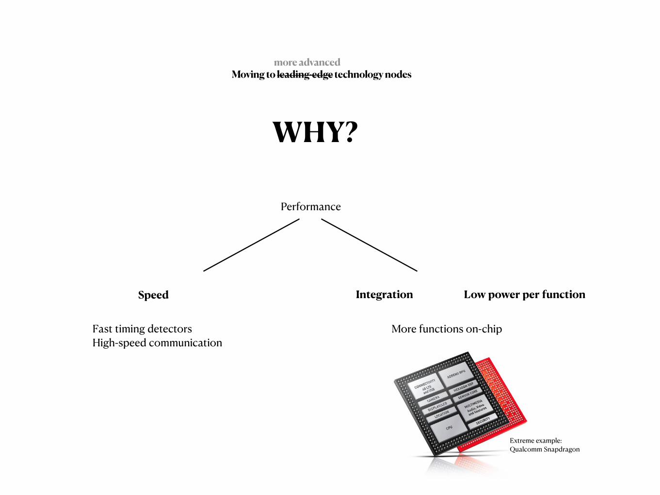
WHY?
Moving to leading-edge technology nodes
Performance
Speed
Fast timing detectors High-speed communication
Low power per functionIntegration
More functions on-chip
more advanced
Extreme example: Qualcomm Snapdragon

WHY?
Moving to leading-edge technology nodesmore advanced
We can do so much more!
….. but it can not be done in the same way

0
500,000
1,000,000
1,500,000
2,000,000
2,500,000
250nm 130nm 65nm 28nm HL-LHCtracker chip
Cost
in $
CMOS node
Cost of a full engineering run
Cost of masks + 600 production wafers (full volume, 130nm)
The increasing complexity in silicon manufacturing is expensive for low-volume ASICs
From: Anysilicon

Silicon is not the only expensive item: IC development requires trained people and advanced software
From: Semiconductor Engineering
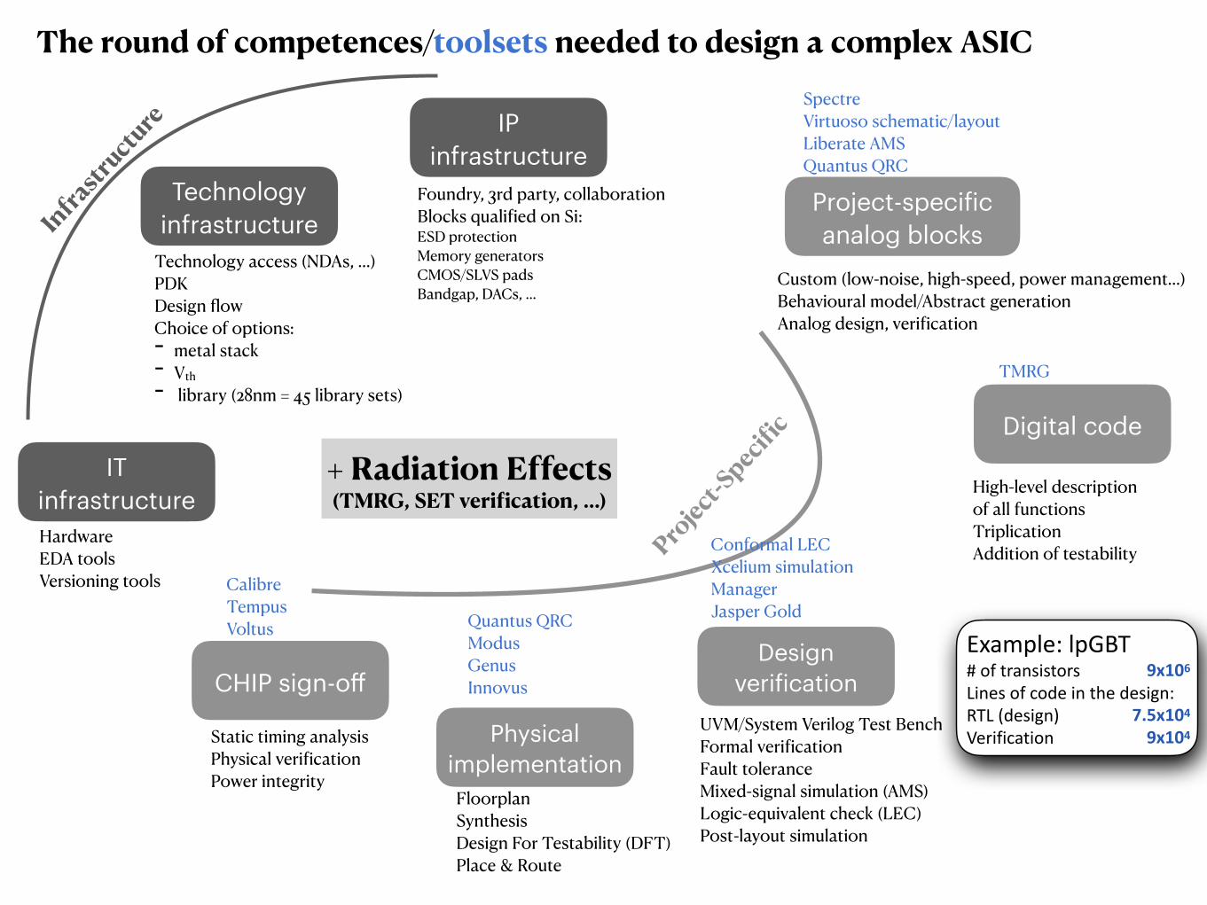
IT infrastructure
Technology infrastructure
IP infrastructure
Project-specific analog blocks
Digital code
Physical implementation
CHIP sign-off
Hardware EDA tools Versioning tools
Technology access (NDAs, …) PDK Design flow Choice of options: - metal stack - Vth - library (28nm = 45 library sets)
Foundry, 3rd party, collaboration Blocks qualified on Si: ESD protection Memory generators CMOS/SLVS pads Bandgap, DACs, …
Custom (low-noise, high-speed, power management…) Behavioural model/Abstract generation Analog design, verification
High-level description of all functions Triplication Addition of testability
Design verification
UVM/System Verilog Test Bench Formal verification Fault tolerance Mixed-signal simulation (AMS) Logic-equivalent check (LEC) Post-layout simulation
Floorplan Synthesis Design For Testability (DFT) Place & Route
Static timing analysis Physical verification Power integrity
The round of competences/toolsets needed to design a complex ASICSpectre Virtuoso schematic/layout Liberate AMS Quantus QRC
TMRG
Quantus QRC Modus Genus Innovus
Calibre Tempus Voltus
Example:lpGBT#oftransistorsLinesofcodeinthedesign:RTL(design)Verification
9x10⁶
7.5x1049x104
Infrastr
ucture
+ Radiation Effects (TMRG, SET verification, …)
Project-
Specific
Conformal LEC Xcelium simulation Manager Jasper Gold
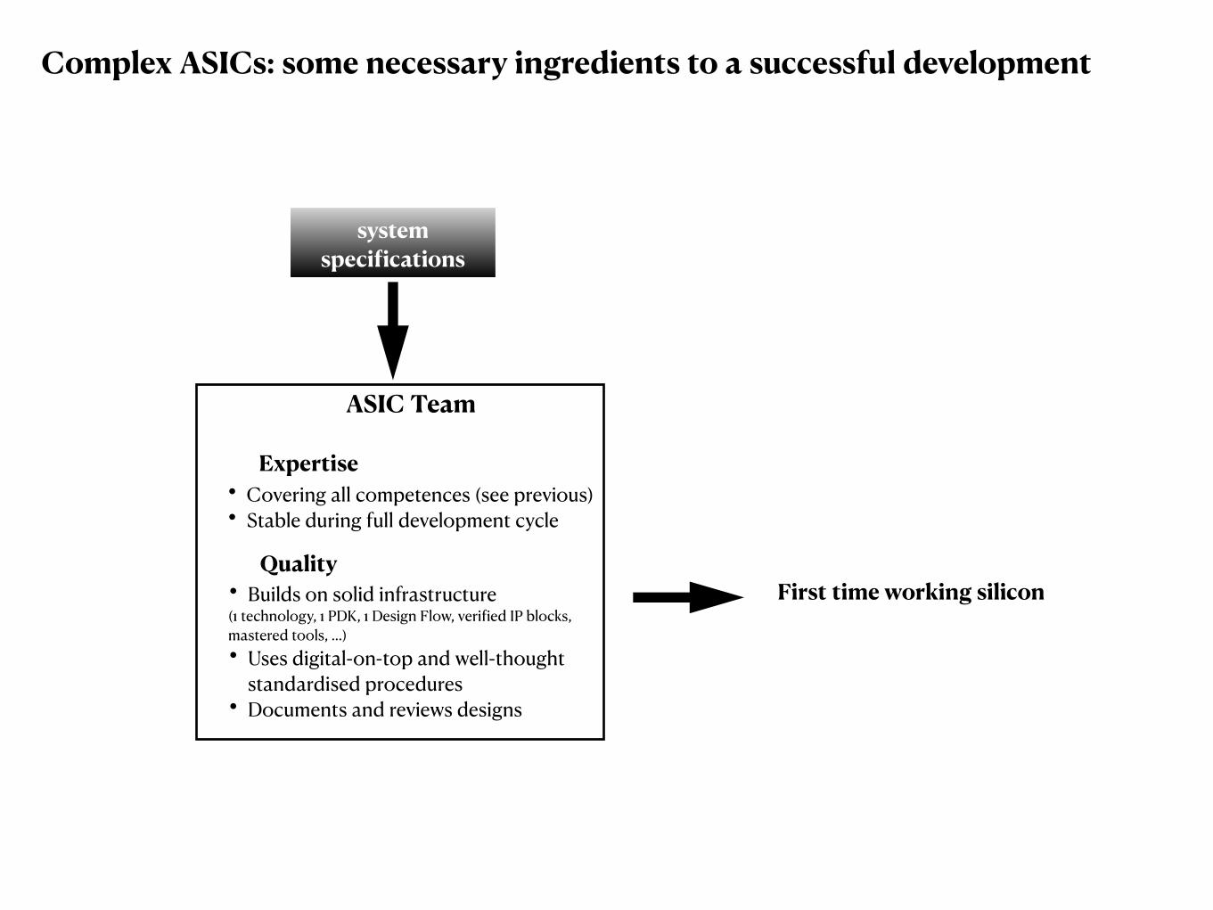
system specifications
Expertise
QualityFirst time working silicon
• Covering all competences (see previous) • Stable during full development cycle
• Builds on solid infrastructure (1 technology, 1 PDK, 1 Design Flow, verified IP blocks, mastered tools, …) • Uses digital-on-top and well-thought
standardised procedures • Documents and reviews designs
ASIC Team
Complex ASICs: some necessary ingredients to a successful development
F
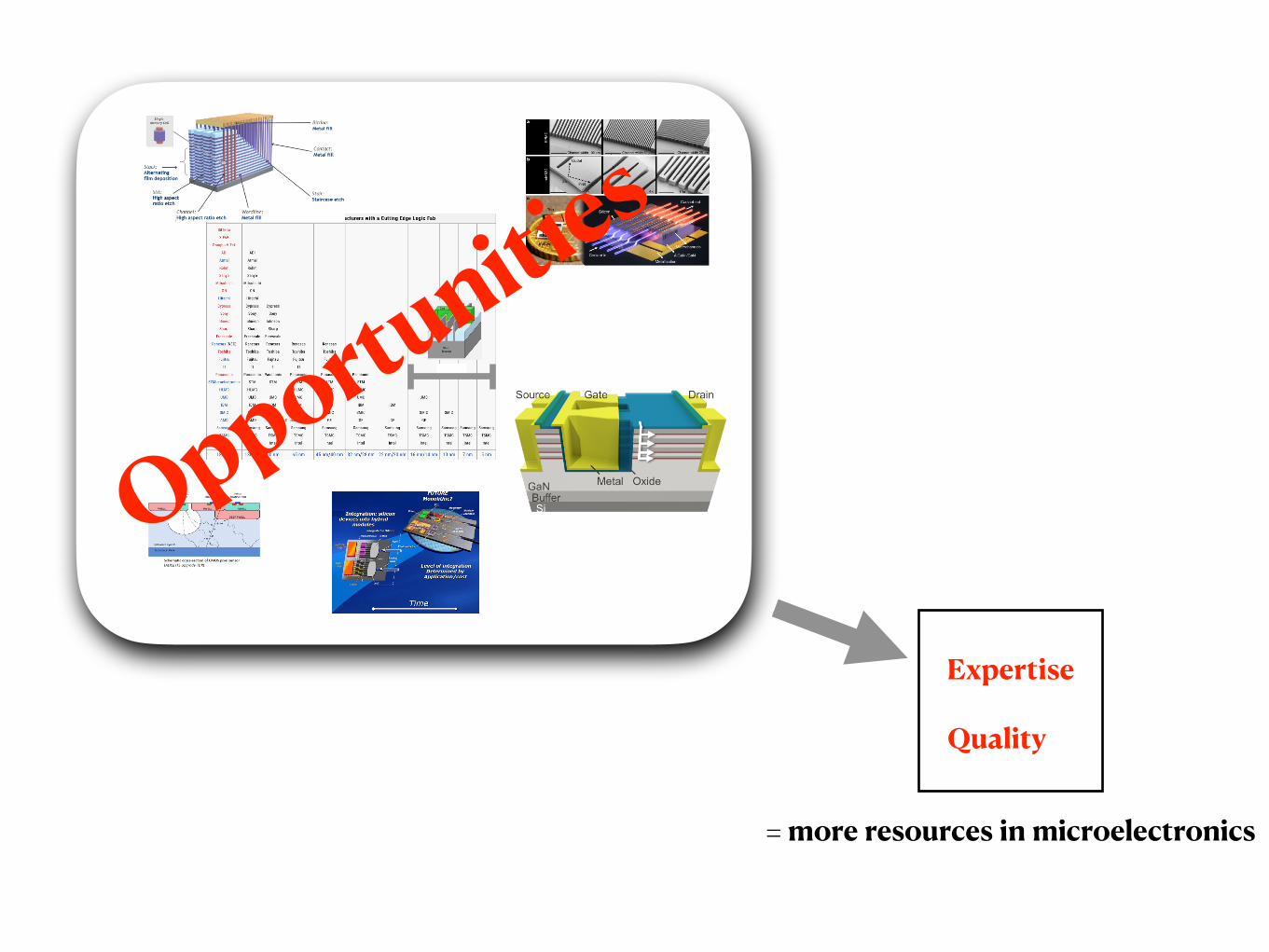
Opportunities
Expertise
Quality
= more resources in microelectronics