Embed Size (px)
Citation preview

Suranaree University of Technology May-Aug 2007
Movement of edge and screw dislocationsMovement of edge and screw dislocations
Formation of a step on the
surface of a crystal by
motion of
(a) An edge dislocation:
the dislocation line moves
in the direction of the
applied shear stress ττττ.
(b) A screw dislocation:
the dislocation line motion
is perpendicular to the
stress direction.
Tapany Udomphol
Suranaree University of Technology May-Aug 2007
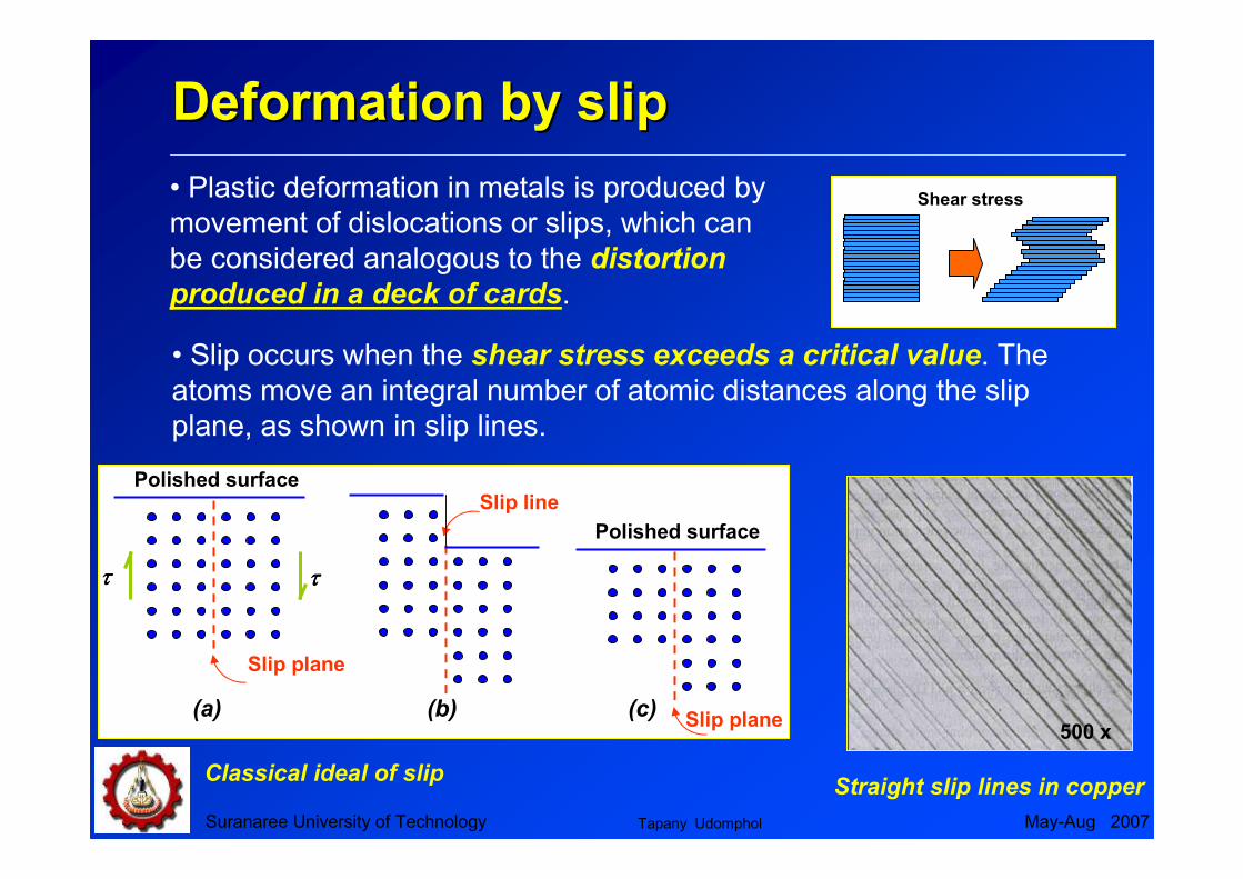
Deformation by slipDeformation by slip
• Slip occurs when the shear stress exceeds a critical value. The
atoms move an integral number of atomic distances along the slip
plane, as shown in slip lines.
Polished surface
Slip plane
ττττ ττττ
Slip line
Polished surface
Slip plane
Classical ideal of slip
(a) (b) (c)
Straight slip lines in copper
• Plastic deformation in metals is produced by
movement of dislocations or slips, which can
be considered analogous to the distortion
produced in a deck of cards.
Shear stress
500 x
Tapany Udomphol
Suranaree University of Technology May-Aug 2007
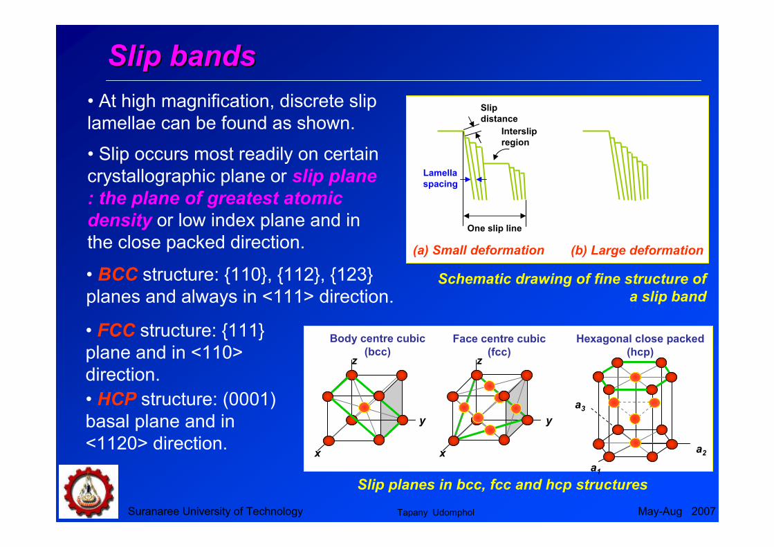
Slip bandsSlip bands
One slip line
Lamella
spacing
Interslip
region
Slip
distance
(a) Small deformation (b) Large deformation
Schematic drawing of fine structure of
a slip band
• At high magnification, discrete slip
lamellae can be found as shown.
• Slip occurs most readily on certain
crystallographic plane or slip plane
: the plane of greatest atomic
density or low index plane and in
the close packed direction.
Body centre cubic
(bcc)
Face centre cubic
(fcc)
Hexagonal close packed
(hcp)
x
z
y
a3
a1
a2
z
y
x
• BCC structure: {110}, {112}, {123}
planes and always in <111> direction.
• FCC structure: {111}
plane and in <110>
direction.
• HCP structure: (0001)
basal plane and in
<1120> direction.
Slip planes in bcc, fcc and hcp structures
Tapany Udomphol
Suranaree University of Technology May-Aug 2007
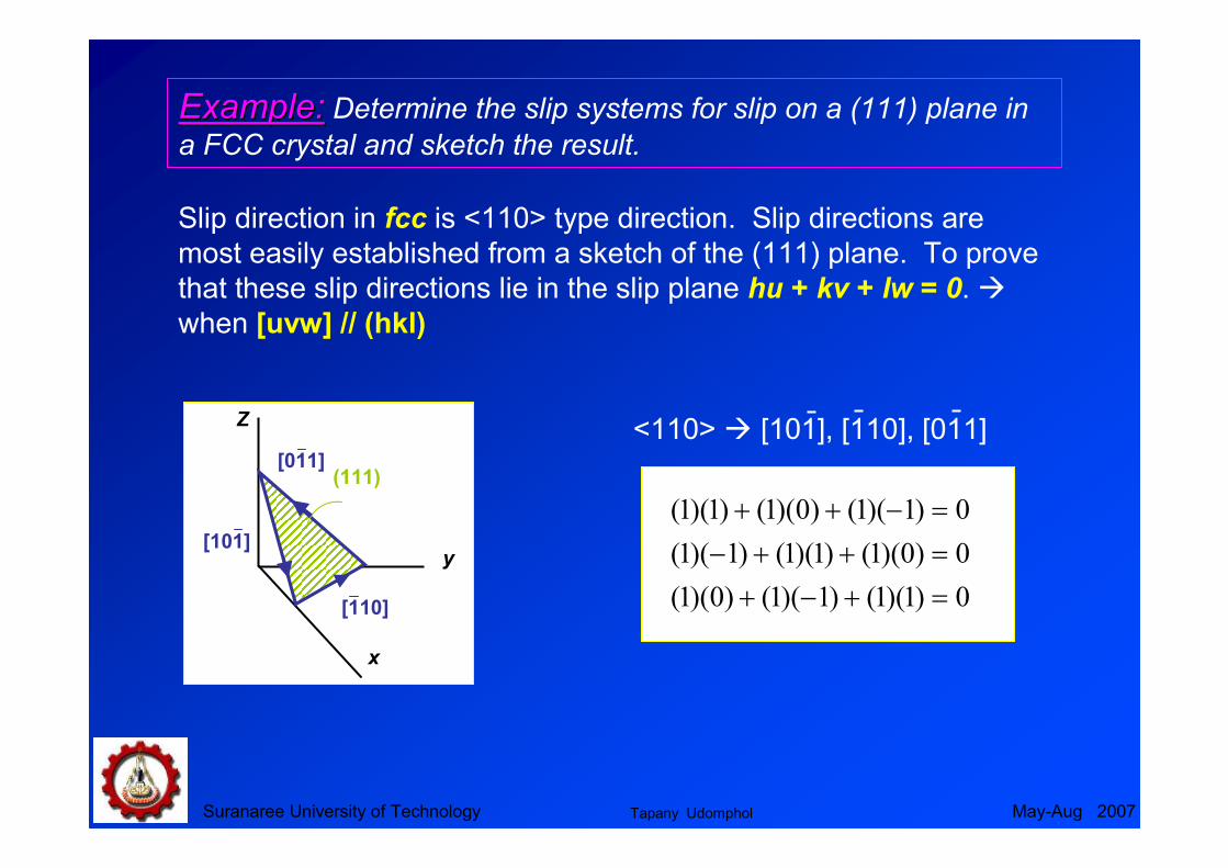
Example:Example: Determine the slip systems for slip on a (111) plane in a FCC crystal and sketch the result.
Slip direction in fcc is <110> type direction. Slip directions are
most easily established from a sketch of the (111) plane. To prove
that these slip directions lie in the slip plane hu + kv + lw = 0. �
when [uvw] // (hkl)
<110> � [101], [110], [011]
0)1)(1()1)(1()0)(1(
0)0)(1()1)(1()1)(1(
0)1)(1()0)(1()1)(1(
=+−+
=++−
=−++
Z
x
y
(111)[011]
[101]
[110]
Tapany Udomphol

Suranaree University of Technology May-Aug 2007
Slip by dislocation motionSlip by dislocation motion
• Slip is a plastic deformation process produced by dislocation motion.
• Dislocation motion is analogous to the caterpillar movement model.
• The caterpillar forms a hump with its position and movement
corresponding to those of extra-half plane in the dislocation model.
Tapany Udomphol

Suranaree University of Technology May-Aug 2007
Energy change in slipEnergy change in slip
Slipped region Unslipped region
Interfacial
region
W
(a)
∆∆∆∆E
Displacement
Slipped state
Unslippedstate
Energy
(b)
• Cottrell considers that plastic
deformation is the transition from an
unslipped to a slipped state by
overcoming an energy barrier ∆∆∆∆E.
• The interfacial region is dislocation of
the width w.
• w interfacial energy
elastic energy
In ductile metals, the dislocation
width is ~ 10 atomic spacing.
When the crystal is complex without highly close-packed planes and
directions, dislocation tends to be immobile ���� brittleness.
Tapany Udomphol
Suranaree University of Technology May-Aug 2007
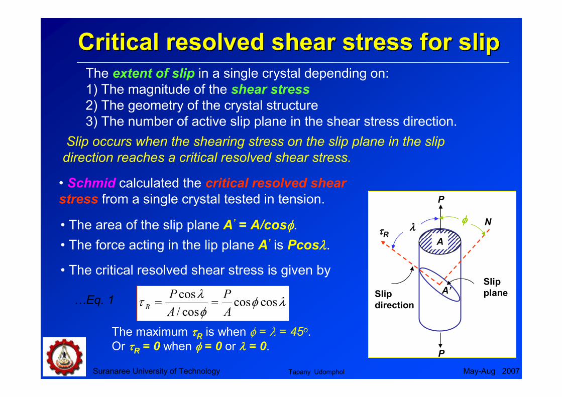
Critical resolved shear stress for slipCritical resolved shear stress for slipThe extent of slip in a single crystal depending on:
1) The magnitude of the shear stress
2) The geometry of the crystal structure
3) The number of active slip plane in the shear stress direction.
Slip occurs when the shearing stress on the slip plane in the slip
direction reaches a critical resolved shear stress.
• Schmid calculated the critical resolved shear
stress from a single crystal tested in tension.
• The area of the slip plane A’ = A/cosφφφφ.
• The force acting in the lip plane A’ is Pcosλλλλ.
N
A
P
ττττR
Slip
direction
Slip
plane
φφφφλλλλ
P
A’
• The critical resolved shear stress is given by
λφφ
λτ coscos
cos/
cos
A
P
A
PR ==…Eq. 1
The maximum ττττR is when φ = λ = 45o.Or ττττR = 0 when φφφφ = 0 or λλλλ = 0.
Tapany Udomphol

Suranaree University of Technology May-Aug 2007
6
2
32
2
)1()1()1()0()1()1(
)1)(0()1)(1()1)(1(cos
222222==
−+−++−+
−+−−+=φ
2
1
22
1
)1()1()0(2
)1)(0()1)(1()0)(1(cos
222==
+−+
−+−−+=λ
From Eq.1 MPaA
P R 7.1462
6
coscos21=
×===
λφ
τσ
The angle between the tensile axis [110] and normal to (111) is
Example:Example: Determine the tensile stress that is applied along the Determine the tensile stress that is applied along the
[110] axis of a silver crystal to cause slip on the (111)[011] [110] axis of a silver crystal to cause slip on the (111)[011]
system. The critical resolved shear stress is 6 MPa.system. The critical resolved shear stress is 6 MPa.
The angle between the tensile axis [110] and slip direction [011] is
Tapany Udomphol

Suranaree University of Technology May-Aug 2007
Critical resolved shear stress Critical resolved shear stress
in real metalsin real metals
Critical resolved
shear stress
Defects
Vacancies
Impurity atoms
Alloying elements
Variation of critical resolved shear stress
with composition in Ag-Au alloy.
The ratio of the resolved shear
stress to the axial stress is called
the Schmid factor m.
λφ coscos=mfactorSchmid
Tapany Udomphol

Suranaree University of Technology May-Aug 2007
Deformation of single crystalsDeformation of single crystals
(a) Tensile
deformation of single
crystal without
constraint.
(b) Rotation of slip
planes due to
constraint.
• In uniaxial tension, the grips
provide constraint making the
slip planes to rotate toward
the tensile axis.
• The increase in length of the specimen depends on the
orientations of the active slip planes and the direction with
the specimen axis.
• When a single crystal is
deformed freely by uniform
glide on every slip plane along
the gauge length without
constraint.
Tapany Udomphol

Suranaree University of Technology May-Aug 2007
Single crystal stressSingle crystal stress--strain curvesstrain curves
Glide shear strain%
Resolved shear stress
Cu
Al
Mg
Zn
Typical single-crystal stress-strain
curves.
FCC metals exhibit greater strain hardening
than HCP metals.
Tapany Udomphol

Suranaree University of Technology May-Aug 2007
Deformation of FCC crystalsDeformation of FCC crystals
Slip system in FCC
metals is {111}<110>.
4 sets of octahedral
{111} planes and each
of which has 3 <110>
directions.
12 potential
slip systems.
(a) A {111}<110> slip system
in FCC unit cell.
(b) The (111) plane from (a) and
three <110> slip directions.
Tapany Udomphol

Suranaree University of Technology May-Aug 2007
Slip systems for FCC, BCC and HCP metalsSlip systems for FCC, BCC and HCP metals
Metals with FCC and BCC
crystal structures have a
relatively large number of slip
systems (at least 12).
Extensive plastic
deformationDuctile
Metals with HCP crystal structure
have few active slip systems.
Less plastic
deformationBrittle
Table 1
Tapany Udomphol

Suranaree University of Technology May-Aug 2007
Deformation by twinningDeformation by twinning
Twinning occurs as atoms on one
side of the boundary (plane) are
located in mirror image positions
of the atoms on the other side.
The boundary is called twinning
boundary.
1) Applied mechanical shear force
(mechanical twin) : in BCC, HCP
2) During annealing heat treatment
(annealing twin) : in FCC.
Twin results from atomic
displacements produced from;
Deformation twins in 3.25% Si iron.
Note: twinning normally occurs when
slip systems are restricted or when
the twinning stress > critical resolved
shear stress.
Schematic diagram of a twin plane
and adjacent atom positions.
Twin plane
(boundary)
Tapany Udomphol

Suranaree University of Technology May-Aug 2007
Twinning Slip
• Similar orientations of the crystal
above and below the slip plane.
Comparisons of twinning and slipComparisons of twinning and slip
• Different orientations of the crystal
above and below the twinning plane.
• Slip normally occurs in discrete
multiples of the atomic
spacing.
• Atom movements in twinning are
much less than an atomic
distance.
• Slip occurs on relatively widely
spaced plane.
• Twinning occurs in a region of
a crystal of every atomic plane
involved in the deformation.
Polished surface
Slip plane
Twin plane
(boundary)
Tapany Udomphol
Suranaree University of Technology May-Aug 2007
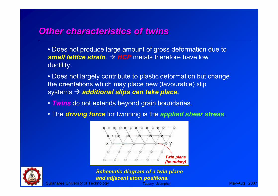
Other characteristics of twinsOther characteristics of twins
• Does not produce large amount of gross deformation due to
small lattice strain. � HCP metals therefore have low
ductility.
• Does not largely contribute to plastic deformation but change
the orientations which may place new (favourable) slip
systems � additional slips can take place.
• Twins do not extends beyond grain boundaries.
• The driving force for twinning is the applied shear stress.
Schematic diagram of a twin plane
and adjacent atom positions.
Twin plane
(boundary)
Tapany Udomphol

Suranaree University of Technology May-Aug 2007
Stacking faultsStacking faults
Stacking faults can be found in metals when there is an
interruption in the stacking sequence.
BA
C
BA
CB
A
CAA
ABCABCA
BA
C
CA
AC
A
ABB
ABCA/CAB
BA
C
CA
B
A
BCC
ABC/ACB/CA
AA
C
ABABAB
ABABAB
Examples:
• Stacking sequence in FCC is
ABC ABC ABC … � ABC AC AB
, Fig (a) �(b).
• Stacking sequence in HCP is
AB AB AB … � AB BA AB
, Fig (d)
(a) FCC packing (b) Deformation
fault in FCC
(c) Twin fault in FCC (d) HCP packing
Note: stacking faults
influence plastic
deformation.
Tapany Udomphol

Suranaree University of Technology May-Aug 2007
Deformation bandsDeformation bands
Deformation bands consist of regions of different orientations
and are formed when material is inhomogeneously deformed.
• Polycrystalline specimens tend to
form these deformation bands
easier than a single crystal.
• Deformation bands are irregular
in shape, poorly defined.
• Observed in FCC and BCC but
not HCP.
Deformation bands in specimen
after tensile test
Tapany Udomphol
Suranaree University of Technology May-Aug 2007
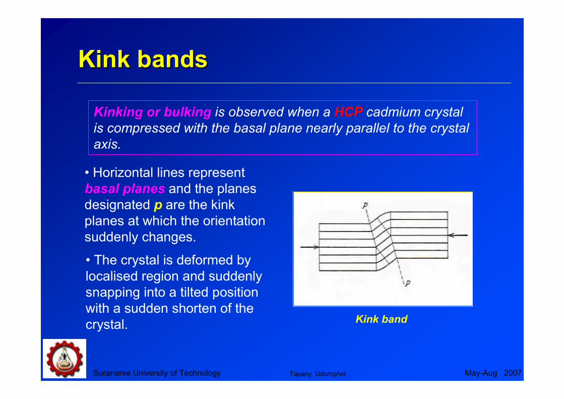
Kink bandsKink bands
Kinking or bulking is observed when a HCP cadmium crystal
is compressed with the basal plane nearly parallel to the crystal
axis.
Kink band
• The crystal is deformed by
localised region and suddenly
snapping into a tilted position
with a sudden shorten of the
crystal.
• Horizontal lines represent
basal planes and the planes
designated p are the kink
planes at which the orientation
suddenly changes.
Tapany Udomphol
Suranaree University of Technology May-Aug 2007
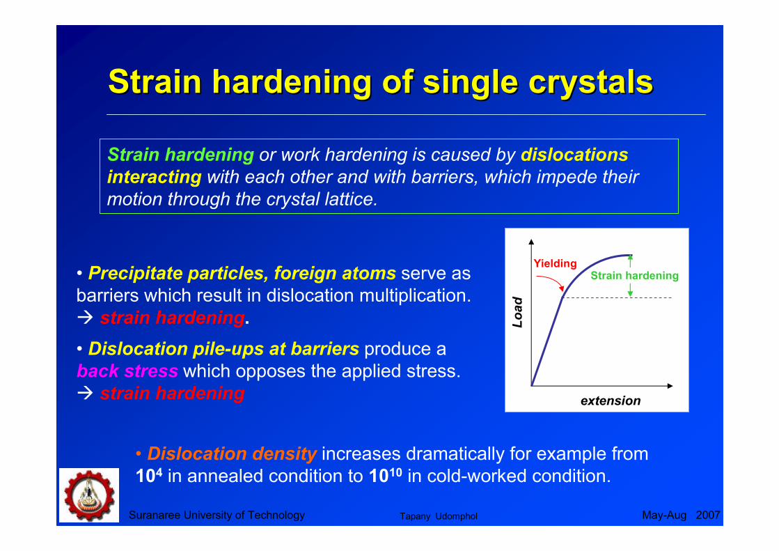
Strain hardening of single crystalsStrain hardening of single crystals
Strain hardening or work hardening is caused by dislocations
interacting with each other and with barriers, which impede their
motion through the crystal lattice.
• Dislocation density increases dramatically for example from
104 in annealed condition to 1010 in cold-worked condition.
• Precipitate particles, foreign atoms serve as
barriers which result in dislocation multiplication.
� strain hardening.
• Dislocation pile-ups at barriers produce a
back stress which opposes the applied stress.
� strain hardening
Load
extension
YieldingStrain hardening
Tapany Udomphol

Suranaree University of Technology May-Aug 2007
Flow curve for FCC single crystalsFlow curve for FCC single crystals
Stage I : easy glide
• Slips occur on only one slip system.
• Dislocation density is low.
• Crystal undergoes little strain
hardening.
• Most dislocations escape from the
crystal to the surface.
Stage II :
• Strain hardening occurs rapidly.
• Slips occur more than one set of
planes. � much higher dislocation
density.
• Dislocation tangles begin to develop.
Stage I : dynamic recovery
• Decreasing rate of strain hardening.
Flow curve for FCC single crystal.
Tapany Udomphol

Suranaree University of Technology May-Aug 2007
References
• Dieter, G.E., Mechanical metallurgy, 1988, SI metric edition,
McGraw-Hill, ISBN 0-07-100406-8.
• Sanford, R.J., Principles of fracture mechanics, 2003, Prentice
Hall, ISBN 0-13-192992-1.
• W.D. Callister, Fundamental of materials science and
engineering/ an interactive e. text., 2001, John Willey & Sons, Inc.,
New York, ISBN 0-471-39551-x.
• Hull, D., Bacon, D.J., Introduction to dislocations, 2001, Forth
edition, Butterworth-Heinemann, ISBN 0-7506-4681-0.
• www.matsci.ucdavis.edu
Tapany Udomphol