Embed Size (px)
Citation preview

Application ReportSNOA040B–August 1999–Revised April 2013
Mounting of Surface Mount Components
ABSTRACT
Over the past few years, electronic products, and especially those which fall within the category ofConsumer Electronics, have been significantly reduced in physical size and weight. This documentprovides information about the techniques used to mount CSP size components.
Contents1 Introduction .................................................................................................................. 32 Component Size Comparison ............................................................................................. 33 Accelerated Bias Moisture Test DIP, SO's, and CSP .................................................................. 44 PCB Assembly Flows ....................................................................................................... 45 Changing Assembly Techniques & Technologies ...................................................................... 8
5.1 Combined Wave Solder and Solder Reflow .................................................................... 85.2 Fine Pitch SM Solder Reflow Side 1 and Side 2 ............................................................... 8
6 Purpose of Solder Paste ................................................................................................... 86.1 Types Of Solder Paste Fluxes ................................................................................... 8
7 Comparison of Particle Size / Shape of Various Solder Pastes ...................................................... 98 Solder Paste For Standard SM Packages ............................................................................... 9
8.1 Solder Paste For Fine Pitch SM Packages ................................................................... 108.2 Water Soluble Solder Paste For Fine Pitch Surface Mount Packages .................................... 108.3 Stencil Thickness ................................................................................................. 108.4 Stencil Materials .................................................................................................. 108.5 Squeegee .......................................................................................................... 108.6 Print Speed ........................................................................................................ 118.7 Print Pressure ..................................................................................................... 118.8 Off And On Contact .............................................................................................. 118.9 Temperature And Humidity ...................................................................................... 118.10 Stencil And Screen Cleaning ................................................................................... 11
9 Component Placement System .......................................................................................... 119.1 System Configuration and Specifications ..................................................................... 119.2 Placement System ............................................................................................... 129.3 Placing Heads ..................................................................................................... 129.4 Componet Types ................................................................................................. 129.5 Component In-Feeding Systems ............................................................................... 129.6 Printed Circuit Board Dimensions .............................................................................. 139.7 Vision Assisted Component Placement ....................................................................... 139.8 Placement Speed ................................................................................................. 139.9 Placement Accuracy ............................................................................................. 139.10 Component Pick-Up Head Types .............................................................................. 149.11 Component Placement Pressure ............................................................................... 14
10 Convection Reflow Furnace .............................................................................................. 1411 Techniques of Solder Interconnection .................................................................................. 14
11.1 Local Component Heating ....................................................................................... 1411.2 Global Board Heating ............................................................................................ 1411.3 Thermal Processing (Reflow) System ......................................................................... 1511.4 Product Throughput .............................................................................................. 15
All trademarks are the property of their respective owners.
1SNOA040B–August 1999–Revised April 2013 Mounting of Surface Mount ComponentsSubmit Documentation Feedback
Copyright © 1999–2013, Texas Instruments Incorporated
www.ti.com
11.5 Thermal Uniformity and Accuracy .............................................................................. 1511.6 Nitrogen Consumption ........................................................................................... 1511.7 Infrared Radiation (I.R.) Reflow Soldering .................................................................... 1511.8 Natural Convection Reflow Soldering .......................................................................... 1511.9 Forced Convection Reflow Soldering .......................................................................... 1511.10 Fixed Convection Reflow Soldering ........................................................................... 1611.11 Heating Zones .................................................................................................... 1611.12 Active Cooling Zones ............................................................................................ 16
12 PCB Assembly Cleaning ................................................................................................. 1613 PCB Cleaning Test ........................................................................................................ 1614 SM Reflow Soldering Reliability ......................................................................................... 1615 Thermal Characteristics of SM Components .......................................................................... 17
List of Figures
1 Molded Dip, SOIC, CSP - 24 Pin ......................................................................................... 3
2 Molded Dip, SOIC, micro-SMD - 8 Pin ................................................................................... 3
3 TSSOP & CSP - 24 pin .................................................................................................... 4
4 Accelerated Environmental Bias Moisture Test Performance......................................................... 4
5 Comparison of Package Temperature vs Wave Soldering Dwell Time for TH Components ..................... 5
6 Immersion in 360°C Solder ................................................................................................ 6
List of Tables
1 Surface Mount Packages Recommended for Wave Solder Immersion ............................................. 7
2 Mounting of Surface Mount Components SNOA040B–August 1999–Revised April 2013Submit Documentation Feedback
Copyright © 1999–2013, Texas Instruments Incorporated
www.ti.com Introduction
1 Introduction
Products such as cellular telephones, lap-top computers, pagers, and camcorders have been reduced byas much as 3/4 of their original introductory size and weight. The most significant contributing factor to thisreduction has been the inclusion of fine pitch, Surface Mount (SM) components. The larger, thicker andheavier leaded Through-Hole (TH) packages consumed far too much power, too much space andcontributed significantly to the total weight of the final product.
Product manufacturers were listening when the customer said "Make it smaller, lighter and lessexpensive".
A second phase to this continued reduction in package size and weight is currently being experienced. Anew family of sub-miniature surface mounted packages known under the industry's generic name of ChipScale Packages (CSP) have recently been introduced. CSP size components are currently the basis of anew series of consumer products. CSP components are currently being supplied in two (2) packageconfiguration, both of which will be a maximum of 1.2 X of the die size. One incorporates planar orbumped pad interconnections on the peripheral of the package underside. The other package is in theform of a reduced scale ball grid array either in a partially or fully populated I/O condition.
The increasing availability of the CSP significantly impacts the ability of product designers to design hand-held products of a size and weight not previously possible. The new CSP allows a higher density ofcomponents to be placed into an increasingly smaller portion of an existing printed circuit board, or thatthe printed circuit board may be reduced with an accompanying reduction in product size, weight and cost.
Chip Scale Packages incorporating high I/O dies, along with discrete passive components are currentlyused in the design of the palm-sized camcorders. As a residual benefit, with components in closerproximity the signal propagation time is reduced thus producing a series of faster circuits.
Accompanying the benefits of smaller size, reduced weight, higher density and increased performance,the individual Methods, Technologies and Techniques used to assemble printed circuit board assemblieshave been impacted.
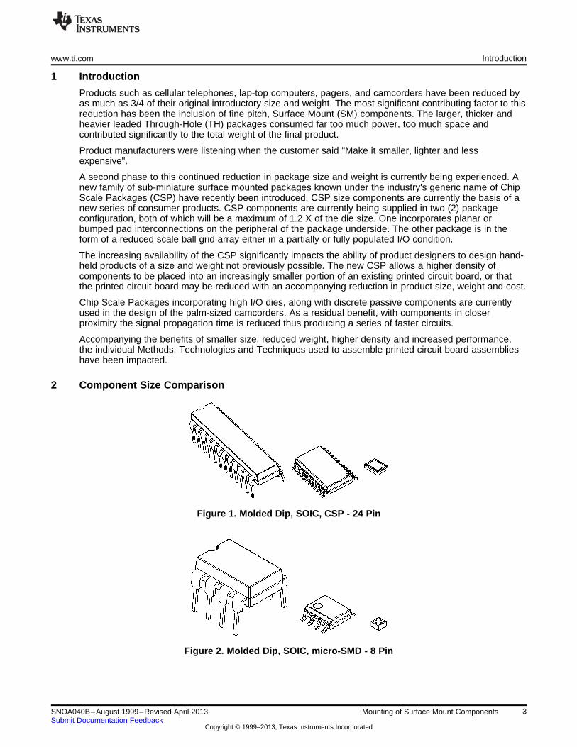
2 Component Size Comparison
Figure 1. Molded Dip, SOIC, CSP - 24 Pin
Figure 2. Molded Dip, SOIC, micro-SMD - 8 Pin
3SNOA040B–August 1999–Revised April 2013 Mounting of Surface Mount ComponentsSubmit Documentation Feedback
Copyright © 1999–2013, Texas Instruments Incorporated
Accelerated Bias Moisture Test DIP, SO's, and CSP www.ti.com
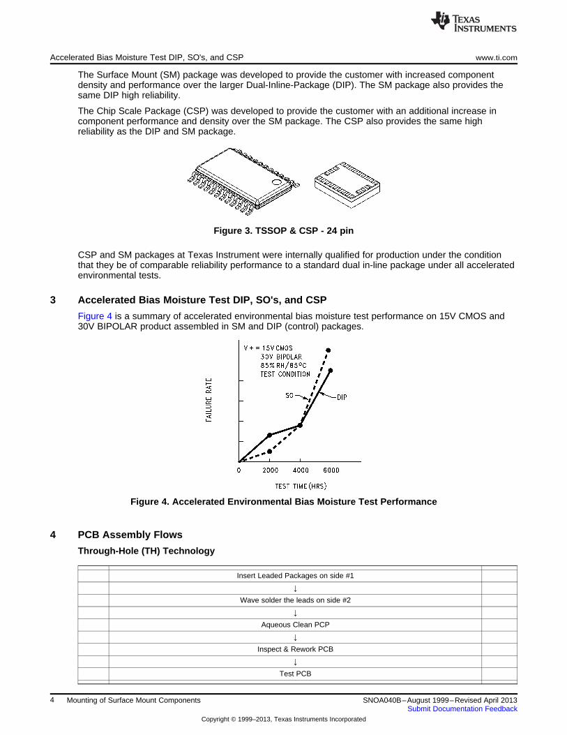
The Surface Mount (SM) package was developed to provide the customer with increased componentdensity and performance over the larger Dual-Inline-Package (DIP). The SM package also provides thesame DIP high reliability.
The Chip Scale Package (CSP) was developed to provide the customer with an additional increase incomponent performance and density over the SM package. The CSP also provides the same highreliability as the DIP and SM package.
Figure 3. TSSOP & CSP - 24 pin
CSP and SM packages at Texas Instrument were internally qualified for production under the conditionthat they be of comparable reliability performance to a standard dual in-line package under all acceleratedenvironmental tests.
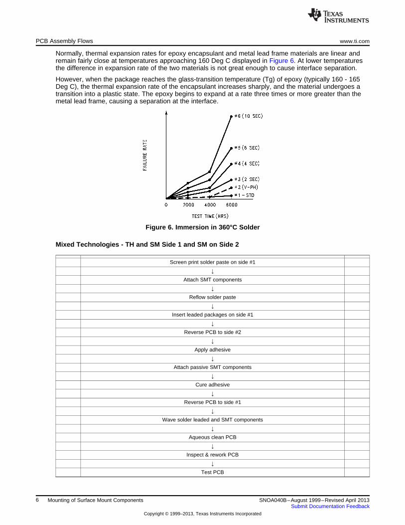
3 Accelerated Bias Moisture Test DIP, SO's, and CSP
Figure 4 is a summary of accelerated environmental bias moisture test performance on 15V CMOS and30V BIPOLAR product assembled in SM and DIP (control) packages.
Figure 4. Accelerated Environmental Bias Moisture Test Performance
4 PCB Assembly Flows
Through-Hole (TH) Technology
Insert Leaded Packages on side #1
↓Wave solder the leads on side #2
↓Aqueous Clean PCP
↓Inspect & Rework PCB
↓Test PCB
4 Mounting of Surface Mount Components SNOA040B–August 1999–Revised April 2013Submit Documentation Feedback
Copyright © 1999–2013, Texas Instruments Incorporated

www.ti.com PCB Assembly Flows
Mixed Technologies - TH Side 1 and Passive SM Side 2
Insert Leaded Packages on side #1
↓Reverse board to side #2
↓Apply adhesive
↓Attach passive SMT components
↓Cure adhesive
↓Reverse board to side #1
↓Wave solder leaded & SMT components
↓Aqueous Clean PCB
↓Inspect & rework PCB
↓Test PCB
Thermal Stress - Side 2 Surface Mount
During the wave solder operation, the side 1 TH components are subjected to significantly less thermalstress than the side 2 bottom side SM mounted components. Only the TH leads come in contact with themolten solder, compared to the entire SM package being immersed in molten solder.
Figure 5 illustrates a comparison of package temperature versus wave soldering dwell time for THcomponents mounted on side 1, with SM packages mounted on side 2.
Figure 5. Comparison of Package Temperature vs Wave Soldering Dwell Time for TH Components
Under ideal conditions, the rate of thermal expansion of package lead frame and plastic encapsulantwould be the same. When both materials expand at the same rate during thermal excursions, bondsbetween metal and plastic maintain a mechanical integrity. Because it is difficult and costly to tailor anepoxy encapsulant material to meet the Coefficient of Thermal Expansion (CTE) of the metal lead frame, amismatch at some point in the thermal excursion will occur, possibly producing an opening by whichcontaminants may enter.
5SNOA040B–August 1999–Revised April 2013 Mounting of Surface Mount ComponentsSubmit Documentation Feedback
Copyright © 1999–2013, Texas Instruments Incorporated
PCB Assembly Flows www.ti.com
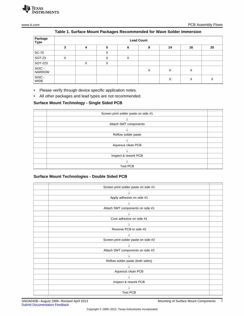
Normally, thermal expansion rates for epoxy encapsulant and metal lead frame materials are linear andremain fairly close at temperatures approaching 160 Deg C displayed in Figure 6. At lower temperaturesthe difference in expansion rate of the two materials is not great enough to cause interface separation.
However, when the package reaches the glass-transition temperature (Tg) of epoxy (typically 160 - 165Deg C), the thermal expansion rate of the encapsulant increases sharply, and the material undergoes atransition into a plastic state. The epoxy begins to expand at a rate three times or more greater than themetal lead frame, causing a separation at the interface.
Figure 6. Immersion in 360°C Solder
Mixed Technologies - TH and SM Side 1 and SM on Side 2
Screen print solder paste on side #1
↓Attach SMT components
↓Reflow solder paste
↓Insert leaded packages on side #1
↓Reverse PCB to side #2
↓Apply adhesive
↓Attach passive SMT components
↓Cure adhesive
↓Reverse PCB to side #1
↓Wave solder leaded and SMT components
↓Aqueous clean PCB
↓Inspect & rework PCB
↓Test PCB
6 Mounting of Surface Mount Components SNOA040B–August 1999–Revised April 2013Submit Documentation Feedback
Copyright © 1999–2013, Texas Instruments Incorporated
www.ti.com PCB Assembly Flows
Table 1. Surface Mount Packages Recommended for Wave Solder Immersion
Package Lead CountType
3 4 5 6 8 14 16 20
SC-70 X
SOT-23 X X X
SOT-223 X X
SOIC - X X XNARROW
SOIC - X X XWIDE
• Please verify through device specific application notes.
• All other packages and lead types are not recommended.
Surface Mount Technology - Single Sided PCB
Screen print solder paste on side #1
↓Attach SMT components
↓Reflow solder paste
↓Aqueous clean PCB
↓Inspect & rework PCB
↓Test PCB
Surface Mount Technologies - Double Sided PCB
Screen print solder paste on side #1
↓Apply adhesive on side #1
↓Attach SMT components on side #1
↓Cure adhesive on side #1
↓Reverse PCB to side #2
↓Screen print solder paste on side #2
↓Attach SMT components on side #2
↓Reflow solder paste (both sides)
↓Aqueous clean PCB
↓Inspect & rework PCB
↓Test PCB
7SNOA040B–August 1999–Revised April 2013 Mounting of Surface Mount ComponentsSubmit Documentation Feedback
Copyright © 1999–2013, Texas Instruments Incorporated

Changing Assembly Techniques & Technologies www.ti.com
5 Changing Assembly Techniques & Technologies
5.1 Combined Wave Solder and Solder Reflow
More mature products incorporating printed circuit boards designed with Through-Hole (TH)semiconductors in a Dual-In-Line (DIP) package and with TH axial leaded components, require bottomside board wave soldering for component to pad interconnection.
Specified packages (see Table 1) may be mounted on the underside (side 2) of the board using this samesolder attachment technique. This assembly technique allows better utilization of the PCB underside, thusfreeing up top side real estate for high lead count active components.
Securement of the bottom side (side 2) SM components is achieved through the use of a cured adhesiveapplied prior to the wave soldering application. Component Engineers responsible for componentsselected for bottom side SM mounted components had to take into consideration that these componentswere subjected to the same time and temperature wave soldering profile experienced by only the leads ofleaded TH components and selected these SM components accordingly.
5.2 Fine Pitch SM Solder Reflow Side 1 and Side 2
Fine pitch SM components are routinely mounted both on side 1 and side 2 with no use of adhesive. Theone exception to this rule is when the component possesses a larger body mass in relation to the strengthof the total volume of solder paste incorporated in the component interconnection.
6 Purpose of Solder Paste
Solder paste provides both the metals and the cleaning agent used to produce the pad interconnection ofpackage lead to printed circuit board pad.
The purpose of the fluxing system within the paste is to provide clean, positive wettable surfaces to whichthe metal solder bonds, thus allowing the electrical interconnection to be produced. The fluxing systemoperates as the cleaning agent required to remove potential oxides from both the package lead/pad andthe board pad. The fluxing system also provides protection of the newly cleaned metal surfaces from re-oxidation during the soldering operation while the lead and pad is at their highest temperature.
6.1 Types Of Solder Paste Fluxes
The fluxing system is composed of a flux and binder system used in solder paste, and is generally dividedinto the categories of Rosin-based, Water Soluble and No-Clean.
Rosin-based fluxes are designated
R Rosin, non-activated
RMA Rosin, mildly activated
RA Rosin, fully activated
Water Soluble fluxes are designated
WS Water-soluble
No-Clean fluxes are designated
NC No-Cleaning required
8 Mounting of Surface Mount Components SNOA040B–August 1999–Revised April 2013Submit Documentation Feedback
Copyright © 1999–2013, Texas Instruments Incorporated

www.ti.com Comparison of Particle Size / Shape of Various Solder Pastes
7 Comparison of Particle Size / Shape of Various Solder Pastes
200 x Alpha (62/36/2) 200 x Kester (63/37)
Solder Paste Screened on Pads 200 x ESL (63/37)
8 Solder Paste For Standard SM Packages
Consistency and uniformity is the key for any successful solder paste material. The basic requirement is astable and homogeneous blend of atomized metal alloy combined with a flux, binder, and solvent systemwhich eliminates the possibility of later separation of the respective materials. These qualities are requiredto ensure a predicable screening and stenciling printing operation producing the required patterndefinition.
The selected solder paste should be formulated so as to eliminate potential breakdown of the metal, flux,binder, and solvents combination, or the premature drying of the solder paste on the printer. Both of thepreviously cited qualities should be in addition to providing a minimum of 48 hours tack time. The selectedsolder paste should be formulated so as to prevent slump and provide over 8 hours of screen working life,with no presence of skipping, scooping and clumping during printing.
For screen printing of standard pitch SM packages, the metal alloy powders should be spherical is shapewith a minimal oxide content and screened to 45-75 micron particle size. The paste should contain aminimum of 88% to 90% metal content, and have a viscosity of 500,000 to 600,000 centipoise.
For stencil printing of standard pitch SM packages, the metal alloy powders shape, size and contentshould remain the same but the viscosity should be increased to 700,000 or 800,000 centipoise.
9SNOA040B–August 1999–Revised April 2013 Mounting of Surface Mount ComponentsSubmit Documentation Feedback
Copyright © 1999–2013, Texas Instruments Incorporated
Solder Paste For Standard SM Packages www.ti.com
In most cases, R, RMA and RA rosin-based fluxes will normally be removed using an aqueous de-ionizedheated water cleaning system, augmented with a saponifier or another surfactant additive. The resultantcleaning water should produce biodegradable saponified products.
8.1 Solder Paste For Fine Pitch SM Packages
Those solder pastes specifically designed for high lead count, fine pitch packages with lead spacing of0.015" require a unique formulation for stenciling, screening and automatic point to point dispensing.
Solder pastes specifically formulated for fine pitch SM components should incorporate all of the previouslycited qualities, plus a flux system developed specifically to ensure that no slumping while still in the wetstage. Fine pitch solder paste should not produce bridging, shorting or solder balling when the pasteexperiences the reflow.
As is in the case of Standard Pitch SM components, R, RMA and RA rosin-based fluxes will normally beremoved using hot de-ionized water, augmented with a surfactant or other additive.
8.2 Water Soluble Solder Paste For Fine Pitch Surface Mount Packages
Water soluble solder pastes should display all of the stencil or screen printing qualities displayed byconventional rosin-based pastes, but should also eliminate the need for chlorofluorocarbons,chlorocarbons or other solvent blends sometimes used for rosin-based flux residue removal.
Although they are soluble in water, water soluble pastes should not be hygroscopic and should beformulated to provide up to 8 hours of screen working life and 48 hours of tack time similar to rosin-basedpastes.
Water soluble, fine solder pastes should be halogen-free. The water-soluble residues should be capable ofbeing cleaned to the extent that they are equivalent in performance, water extract resistivity and SIRvalues to standard RMA fluxes. Flux residues should be able to be removed with a cool presoak followedby a 140 Deg. F spray.
8.3 Stencil Thickness
SM Lead Pitch
inch mm
0.050 1.27
0.025 0.63
0.015 to 0.020 0.4 to 0.5
Recommended Stencil Thickness
inch mm
0.008 to 0.010 0.20 to 0.25
0.006 to 0.008 0.15 to 0.20
0.004 to 0.006 0.10 to 0.15
8.4 Stencil Materials
Stainless Steel is the most prevalent material used to produce stencils, but brass, Alloy 42, molybdenumand nickel plated brass are also used.
8.5 Squeegee
Metal is the most common material used to produce squeegees. The justification for the use of metal isthat it produces a uniform surface across the top surface of the stencil without scooping down into the justdeposited solder paste.
Rubber of an 80 to 90 Durometer reading is also used.
10 Mounting of Surface Mount Components SNOA040B–August 1999–Revised April 2013Submit Documentation Feedback
Copyright © 1999–2013, Texas Instruments Incorporated

www.ti.com Component Placement System
8.6 Print Speed
Printing speeds of 0.5 to 2.5 inches (15 to 65 mm) per second are normally used, depending on type andcapabilities of the solder printing machine.
8.7 Print Pressure
During the solder paste printing operation, sufficient downward pressure should be exerted by thesqueegee against the stencil surface to wipe the stencil clean. Although the printing pressure will vary withthe type of printer, typically a pressure of 1.25 to 2.5 lbs per inch of squeegee length is acceptable.
8.8 Off And On Contact
Both contact and non-contact techniques are used successfully. If non-contact is used, a snap-off of up to0.005 is recommended.
8.9 Temperature And Humidity
The screen printing of solder paste should be performed between a temperature of 68° to 78° F (20° to26° C). The relative humidity of the application area should be kept between 35% to 65%. Solder pastenot applied to printed circuit boards should not be returned to the container from which it was taken.
8.10 Stencil And Screen Cleaning
Stencils and screens should be cleaned of unused solder paste using water heated to a minimum of 140Deg F in conjunction with a pressure spray. Although the initial water need not be deionized, it isrecommended that a final rinse be performed using deionized water, followed by an isopropanol rinse.This same procedure should also be followed for any hand tools and the squeegee used to apply thesolder paste.
At no time should the stencil, screen or tools which have come in contact with unreflowed solder paste becleaned in equipment used to clean printed circuit boards of reflowed solder paste residues.
9 Component Placement System
9.1 System Configuration and Specifications
Product designs continue to demand continued down-sizing of the component package, accompanied byhigher board densities. The component placement system must accommodate these trends by employinga highly accurate, computer controlled, camera directed placement nozzle that is responsible forconstraining the component during pick-up through push-off after placement.
Following are some of the more significant elements devised by the system vendors there by enabling theplacement system to produce high speed, high density accurate component placements:
• Computer controller
• Windows or vendor software
• Vision correction system
• Component body height adjustment
• Z-Axis placement programmability
• Single Head - Multiple programmable nozzles
• Dual Head - Multiple programmable nozzles
• Dual Head - 6 nozzles per head
• Dual Work Table - 12 heads with 3 nozzles per head
11SNOA040B–August 1999–Revised April 2013 Mounting of Surface Mount ComponentsSubmit Documentation Feedback
Copyright © 1999–2013, Texas Instruments Incorporated
Component Placement System www.ti.com
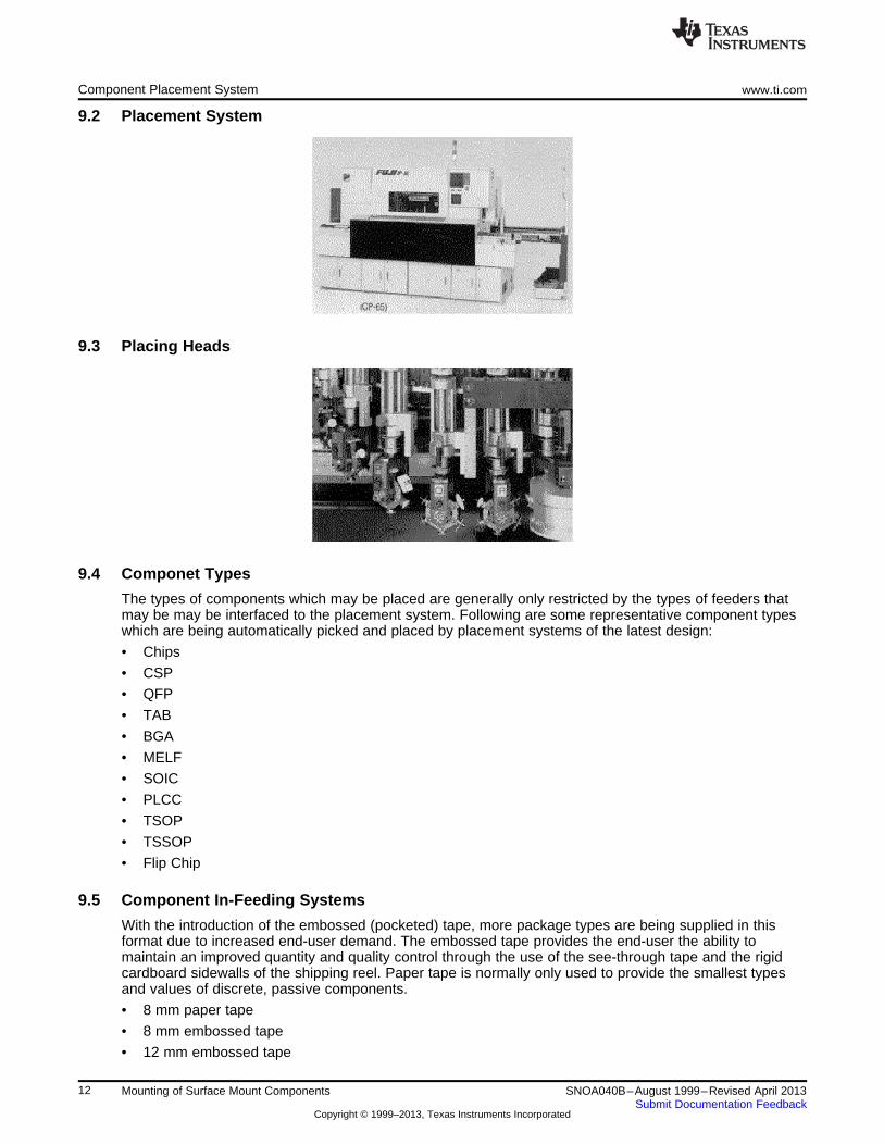
9.2 Placement System
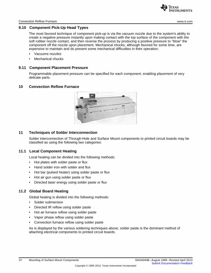
9.3 Placing Heads
9.4 Componet Types
The types of components which may be placed are generally only restricted by the types of feeders thatmay be may be interfaced to the placement system. Following are some representative component typeswhich are being automatically picked and placed by placement systems of the latest design:
• Chips
• CSP
• QFP
• TAB
• BGA
• MELF
• SOIC
• PLCC
• TSOP
• TSSOP
• Flip Chip
9.5 Component In-Feeding Systems
With the introduction of the embossed (pocketed) tape, more package types are being supplied in thisformat due to increased end-user demand. The embossed tape provides the end-user the ability tomaintain an improved quantity and quality control through the use of the see-through tape and the rigidcardboard sidewalls of the shipping reel. Paper tape is normally only used to provide the smallest typesand values of discrete, passive components.
• 8 mm paper tape
• 8 mm embossed tape
• 12 mm embossed tape
12 Mounting of Surface Mount Components SNOA040B–August 1999–Revised April 2013Submit Documentation Feedback
Copyright © 1999–2013, Texas Instruments Incorporated

www.ti.com Component Placement System
• 16 mm embossed tape
• 24 mm embossed tape
• 32 mm embossed tape
• 48 mm embossed tape
• Stick in-feeding
• Tray in-feeding
• Ultra-small chips up to 4.5 mm
• Medium-sized odd form components up to 28.0 mm
• Large odd form components up to 38.0 mm
• Extremely large odd form components up to 74.0 mm
9.6 Printed Circuit Board Dimensions
Current placement systems are designed to provide the end user with the maximum printed circuit boardsize in both the X and Y axis. Most of the current designs will allow a change in the conveyor rail width tobe automatically executed by servo motors by program commands conveyed through the computercontroller.
• Min. 80 x 50 mm (3 x 2")
• Max. 508 x 457 mm (20 x 18")
9.7 Vision Assisted Component Placement
The vision system should include as a basis element of the design, an ability to process (establishX/Y/Theta) the component location on the pick-up head and match the component to the respectivecomponent pads. To achieve the required placement accuracy, the following is necessary:
• Gray scale vision processing
• Component placement algorithms
• Fiducial (local and global) camera
• Component pad/lead recognition camera
9.8 Placement Speed
Although placement speed is typically quoted at approximately 0.1 second per placement, Flip Chipcomponents can take as long as 3.5 to 5.0 seconds per shot (placement). Component placement speed isdependent upon such factors as distance which the placement head must travel between component pick-up and placement location, and the requirement to view the component leads/pads for component-to-padalignment prior to placement
• Min. 0. 09 sec. per component
• Max. 0. 12 sec. per component
9.9 Placement Accuracy
The accuracy to which the component is aligned and placed on the solder pads is contingent upon severalfactors, such as use of local fiducial marks; datum point location; size of printed circuit board; and flatnessof printed circuit board.
• Min. ± 0.025 mm (using local fiducial marks)
• Max. ± 0.1 mm
13SNOA040B–August 1999–Revised April 2013 Mounting of Surface Mount ComponentsSubmit Documentation Feedback
Copyright © 1999–2013, Texas Instruments Incorporated
Convection Reflow Furnace www.ti.com
9.10 Component Pick-Up Head Types
The most favored technique of component pick-up is via the vacuum nozzle due to the system's ability tocreate a negative pressure instantly upon making contact with the top surface of the component with thesoft rubber nozzle contact, and then reverse the process by producing a positive pressure to "blow" thecomponent off the nozzle upon placement. Mechanical chucks, although favored for some time, areexpensive to maintain and do present some mechanical difficulties in their operation.
• Vacuums nozzles
• Mechanical chucks
9.11 Component Placement Pressure
Programmable placement pressure can be specified for each component, enabling placement of verydelicate parts.
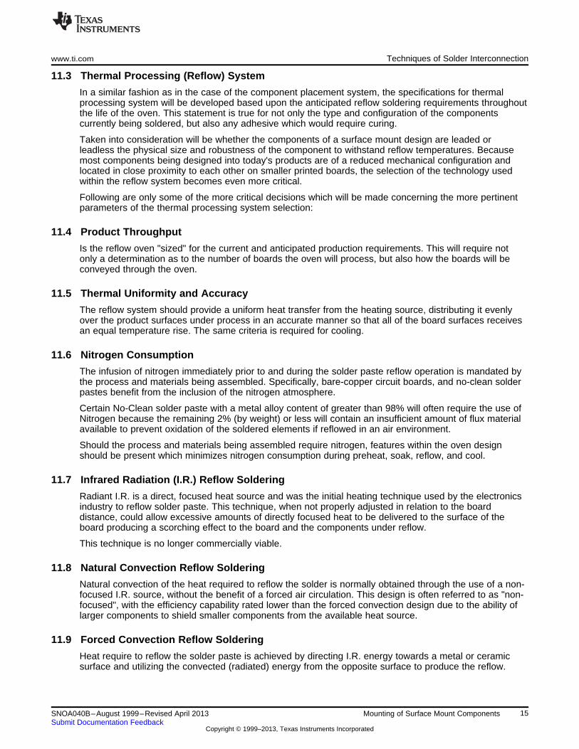
10 Convection Reflow Furnace
11 Techniques of Solder Interconnection
Solder interconnection of Through-Hole and Surface Mount components to printed circuit boards may beclassified as using the following two categories:
11.1 Local Component Heating
Local heating can be divided into the following methods:
• Hot plates with solder paste or flux
• Hand solder iron with solder and flux
• Hot bar (pulsed heater) using solder paste or flux
• Hot air gun using solder paste or flux
• Directed laser energy using solder paste or flux
11.2 Global Board Heating
Global heating is divided into the following methods:
• Solder submersion
• Directed IR reflow using solder paste
• Hot air furnace reflow using solder paste
• Vapor phase reflow using solder paste
• Convection furnace reflow using solder paste
As is displayed by the various soldering techniques above, solder paste is the dominant method ofattaching electrical components to printed circuit boards.
14 Mounting of Surface Mount Components SNOA040B–August 1999–Revised April 2013Submit Documentation Feedback
Copyright © 1999–2013, Texas Instruments Incorporated
www.ti.com Techniques of Solder Interconnection
11.3 Thermal Processing (Reflow) System
In a similar fashion as in the case of the component placement system, the specifications for thermalprocessing system will be developed based upon the anticipated reflow soldering requirements throughoutthe life of the oven. This statement is true for not only the type and configuration of the componentscurrently being soldered, but also any adhesive which would require curing.
Taken into consideration will be whether the components of a surface mount design are leaded orleadless the physical size and robustness of the component to withstand reflow temperatures. Becausemost components being designed into today's products are of a reduced mechanical configuration andlocated in close proximity to each other on smaller printed boards, the selection of the technology usedwithin the reflow system becomes even more critical.
Following are only some of the more critical decisions which will be made concerning the more pertinentparameters of the thermal processing system selection:
11.4 Product Throughput
Is the reflow oven "sized" for the current and anticipated production requirements. This will require notonly a determination as to the number of boards the oven will process, but also how the boards will beconveyed through the oven.
11.5 Thermal Uniformity and Accuracy
The reflow system should provide a uniform heat transfer from the heating source, distributing it evenlyover the product surfaces under process in an accurate manner so that all of the board surfaces receivesan equal temperature rise. The same criteria is required for cooling.
11.6 Nitrogen Consumption
The infusion of nitrogen immediately prior to and during the solder paste reflow operation is mandated bythe process and materials being assembled. Specifically, bare-copper circuit boards, and no-clean solderpastes benefit from the inclusion of the nitrogen atmosphere.
Certain No-Clean solder paste with a metal alloy content of greater than 98% will often require the use ofNitrogen because the remaining 2% (by weight) or less will contain an insufficient amount of flux materialavailable to prevent oxidation of the soldered elements if reflowed in an air environment.
Should the process and materials being assembled require nitrogen, features within the oven designshould be present which minimizes nitrogen consumption during preheat, soak, reflow, and cool.
11.7 Infrared Radiation (I.R.) Reflow Soldering
Radiant I.R. is a direct, focused heat source and was the initial heating technique used by the electronicsindustry to reflow solder paste. This technique, when not properly adjusted in relation to the boarddistance, could allow excessive amounts of directly focused heat to be delivered to the surface of theboard producing a scorching effect to the board and the components under reflow.
This technique is no longer commercially viable.
11.8 Natural Convection Reflow Soldering
Natural convection of the heat required to reflow the solder is normally obtained through the use of a non-focused I.R. source, without the benefit of a forced air circulation. This design is often referred to as "non-focused", with the efficiency capability rated lower than the forced convection design due to the ability oflarger components to shield smaller components from the available heat source.
11.9 Forced Convection Reflow Soldering
Heat require to reflow the solder paste is achieved by directing I.R. energy towards a metal or ceramicsurface and utilizing the convected (radiated) energy from the opposite surface to produce the reflow.
15SNOA040B–August 1999–Revised April 2013 Mounting of Surface Mount ComponentsSubmit Documentation Feedback
Copyright © 1999–2013, Texas Instruments Incorporated
PCB Assembly Cleaning www.ti.com
The heat is circulated within the reflow zones by strategically located fans. By use of a non-directed,convected heat circulated via strategically located fans, hot spots on the boards can potentially beeliminated.
11.10 Fixed Convection Reflow Soldering
Fixed Convection reflow soldering utilizes much of the same technology as Forced Convection with theexception of the use of strategically located fans.
11.11 Heating Zones
The number of heating zones required will be determined by current and anticipated product throughputrequirements, product size and physical mass, product orientation within the oven while on the conveyor,and requirements dictated by the particular solder paste reflow profile. Reflow ovens are typically offeredin ranges from four to 12 heating zones.
11.12 Active Cooling Zones
Active cooling zones should be positioned immediately adjacent to the heating zones and should beideally provided to meet the reflow requirements specified by the solder paste manufacturer.
The amount of cooling required may also be dictated by product handling or subsequent assemblyoperations following reflow.
Depending on the system requirements and vendor capability, the number of cooling zones which may beincorporated into the system may range from one to 12.
12 PCB Assembly Cleaning
If the printed circuit boards were assembled using a rosin based or other flux system which requiresremoval from the board surface after reflow, the subsequent cleaning operation should be performed asshortly after reflow as possible.
The timely initiation of the cleaning operation is dictated by the ability of the flux to collect and harden withadditional residues under and around traces and the bodies of components. The lack of attention to thetimely removal of this residue present additional and unneeded removal difficulties, with the possibility thatsome contaminates may be trapped in flux and remain on the surface of the board to potentiallycompromise qualities for the finished product.
13 PCB Cleaning Test
Upon completion of the solder reflow operation, the surface mount assembly should be tested for ionicand other contaminates using recognized specification, such as IPC-6012.
If the printed circuit board is to have a permanent solder mask coating applied, the bare uncoated boardshould be also tested for ionic and other contaminates prior to permanent coating.
14 SM Reflow Soldering Reliability
More recently designed products utilizing the low profile, high lead count, fine pitch SM components, whencombined with Chip Scale Packages present additional challenges to the techniques and technologies ofhigh reliability component interconnection.
The potential obstacles of high reliability fine pitch SM and reduced size CSP component interconnectionsare contingent upon a number of parameters, with the most prevalent being the following:
• Technology and package construction
• Quality and repeatability of the reflow process
• Metallurgy and uniformity of both the solder paste and interconnection pad plating
• Individual board design, both internally and externally
• Conditions in which the product will be used
• The intended product life
16 Mounting of Surface Mount Components SNOA040B–August 1999–Revised April 2013Submit Documentation Feedback
Copyright © 1999–2013, Texas Instruments Incorporated

www.ti.com Thermal Characteristics of SM Components
Reliability level demands are higher for products using the new low profile, fine-pitch, high lead countminiature IC packages, such as CSP and reduced size BGA over assemblies built around older, moreconventional packages with their longer and more compliant leads.
15 Thermal Characteristics of SM Components
Both Chip Scale Packages and SM components are typically fabricated using a combination of either ametal lead frame; laminated substrate; ceramic substrate, or flexible film substrate as a base on which adie is adhesively attached. Gold wires are bonded from die to lead frame/substrate, and the unit isencapsulated, with a thermoset epoxy.
Because each material has different rate of thermal expansion, the thermal characteristics of the materialsgenerally correspond to a Thermal Mechanical Analysis (TMA) graph.
17SNOA040B–August 1999–Revised April 2013 Mounting of Surface Mount ComponentsSubmit Documentation Feedback
Copyright © 1999–2013, Texas Instruments Incorporated

IMPORTANT NOTICE
Texas Instruments Incorporated and its subsidiaries (TI) reserve the right to make corrections, enhancements, improvements and otherchanges to its semiconductor products and services per JESD46, latest issue, and to discontinue any product or service per JESD48, latestissue. Buyers should obtain the latest relevant information before placing orders and should verify that such information is current andcomplete. All semiconductor products (also referred to herein as “components”) are sold subject to TI’s terms and conditions of salesupplied at the time of order acknowledgment.
TI warrants performance of its components to the specifications applicable at the time of sale, in accordance with the warranty in TI’s termsand conditions of sale of semiconductor products. Testing and other quality control techniques are used to the extent TI deems necessaryto support this warranty. Except where mandated by applicable law, testing of all parameters of each component is not necessarilyperformed.
TI assumes no liability for applications assistance or the design of Buyers’ products. Buyers are responsible for their products andapplications using TI components. To minimize the risks associated with Buyers’ products and applications, Buyers should provideadequate design and operating safeguards.
TI does not warrant or represent that any license, either express or implied, is granted under any patent right, copyright, mask work right, orother intellectual property right relating to any combination, machine, or process in which TI components or services are used. Informationpublished by TI regarding third-party products or services does not constitute a license to use such products or services or a warranty orendorsement thereof. Use of such information may require a license from a third party under the patents or other intellectual property of thethird party, or a license from TI under the patents or other intellectual property of TI.
Reproduction of significant portions of TI information in TI data books or data sheets is permissible only if reproduction is without alterationand is accompanied by all associated warranties, conditions, limitations, and notices. TI is not responsible or liable for such altereddocumentation. Information of third parties may be subject to additional restrictions.
Resale of TI components or services with statements different from or beyond the parameters stated by TI for that component or servicevoids all express and any implied warranties for the associated TI component or service and is an unfair and deceptive business practice.TI is not responsible or liable for any such statements.
Buyer acknowledges and agrees that it is solely responsible for compliance with all legal, regulatory and safety-related requirementsconcerning its products, and any use of TI components in its applications, notwithstanding any applications-related information or supportthat may be provided by TI. Buyer represents and agrees that it has all the necessary expertise to create and implement safeguards whichanticipate dangerous consequences of failures, monitor failures and their consequences, lessen the likelihood of failures that might causeharm and take appropriate remedial actions. Buyer will fully indemnify TI and its representatives against any damages arising out of the useof any TI components in safety-critical applications.
In some cases, TI components may be promoted specifically to facilitate safety-related applications. With such components, TI’s goal is tohelp enable customers to design and create their own end-product solutions that meet applicable functional safety standards andrequirements. Nonetheless, such components are subject to these terms.
No TI components are authorized for use in FDA Class III (or similar life-critical medical equipment) unless authorized officers of the partieshave executed a special agreement specifically governing such use.
Only those TI components which TI has specifically designated as military grade or “enhanced plastic” are designed and intended for use inmilitary/aerospace applications or environments. Buyer acknowledges and agrees that any military or aerospace use of TI componentswhich have not been so designated is solely at the Buyer's risk, and that Buyer is solely responsible for compliance with all legal andregulatory requirements in connection with such use.
TI has specifically designated certain components as meeting ISO/TS16949 requirements, mainly for automotive use. In any case of use ofnon-designated products, TI will not be responsible for any failure to meet ISO/TS16949.
Products Applications
Audio www.ti.com/audio Automotive and Transportation www.ti.com/automotive
Amplifiers amplifier.ti.com Communications and Telecom www.ti.com/communications
Data Converters dataconverter.ti.com Computers and Peripherals www.ti.com/computers
DLP® Products www.dlp.com Consumer Electronics www.ti.com/consumer-apps
DSP dsp.ti.com Energy and Lighting www.ti.com/energy
Clocks and Timers www.ti.com/clocks Industrial www.ti.com/industrial
Interface interface.ti.com Medical www.ti.com/medical
Logic logic.ti.com Security www.ti.com/security
Power Mgmt power.ti.com Space, Avionics and Defense www.ti.com/space-avionics-defense
Microcontrollers microcontroller.ti.com Video and Imaging www.ti.com/video
RFID www.ti-rfid.com
OMAP Applications Processors www.ti.com/omap TI E2E Community e2e.ti.com
Wireless Connectivity www.ti.com/wirelessconnectivity
Mailing Address: Texas Instruments, Post Office Box 655303, Dallas, Texas 75265Copyright © 2013, Texas Instruments Incorporated