Embed Size (px)
Citation preview
Advance Information
MC145572EVK
ISDN U-Interface Transceiver Evaluation Kit
This document contains information on a new product. SpeciÞcations and information herein are subject to change without notice.
Order this documentby MC145572EVK/D
MOTOROLASEMICONDUCTOR TECHNICAL DATA
REV 211/97
Fre
esc
ale
Se
mic
on
du
cto
r, I
Freescale Semiconductor, Inc.
For More Information On This Product, Go to: www.freescale.com
nc
...
3MC145572EVK
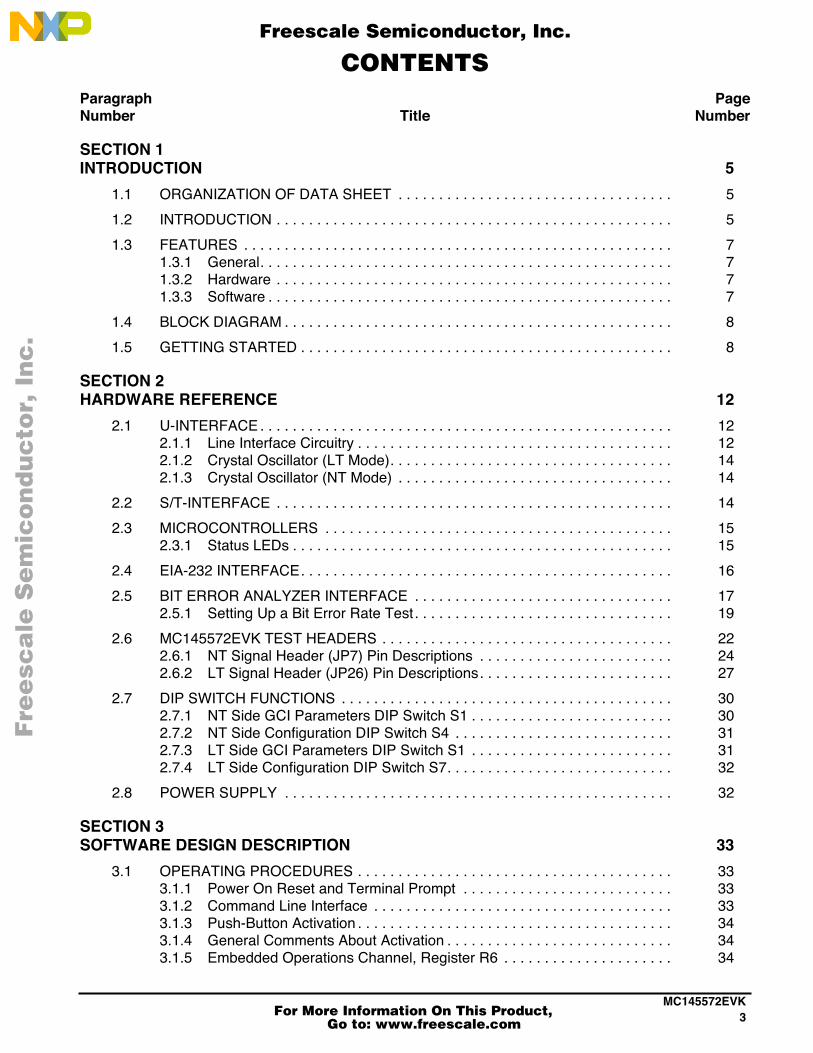
CONTENTS
Paragraph PageNumber Title Number
SECTION 1INTRODUCTION 5
1.1 ORGANIZATION OF DATA SHEET . . . . . . . . . . . . . . . . . . . . . . . . . . . . . . . . . . 5
1.2 INTRODUCTION . . . . . . . . . . . . . . . . . . . . . . . . . . . . . . . . . . . . . . . . . . . . . . . . . 5
1.3 FEATURES . . . . . . . . . . . . . . . . . . . . . . . . . . . . . . . . . . . . . . . . . . . . . . . . . . . . . 71.3.1 General. . . . . . . . . . . . . . . . . . . . . . . . . . . . . . . . . . . . . . . . . . . . . . . . . . . 71.3.2 Hardware . . . . . . . . . . . . . . . . . . . . . . . . . . . . . . . . . . . . . . . . . . . . . . . . . 71.3.3 Software . . . . . . . . . . . . . . . . . . . . . . . . . . . . . . . . . . . . . . . . . . . . . . . . . . 7
1.4 BLOCK DIAGRAM . . . . . . . . . . . . . . . . . . . . . . . . . . . . . . . . . . . . . . . . . . . . . . . . 8
1.5 GETTING STARTED . . . . . . . . . . . . . . . . . . . . . . . . . . . . . . . . . . . . . . . . . . . . . . 8
SECTION 2HARDWARE REFERENCE 12
2.1 U-INTERFACE . . . . . . . . . . . . . . . . . . . . . . . . . . . . . . . . . . . . . . . . . . . . . . . . . . . 122.1.1 Line Interface Circuitry . . . . . . . . . . . . . . . . . . . . . . . . . . . . . . . . . . . . . . . 122.1.2 Crystal Oscillator (LT Mode). . . . . . . . . . . . . . . . . . . . . . . . . . . . . . . . . . . 142.1.3 Crystal Oscillator (NT Mode) . . . . . . . . . . . . . . . . . . . . . . . . . . . . . . . . . . 14
2.2 S/T-INTERFACE . . . . . . . . . . . . . . . . . . . . . . . . . . . . . . . . . . . . . . . . . . . . . . . . . 14
2.3 MICROCONTROLLERS . . . . . . . . . . . . . . . . . . . . . . . . . . . . . . . . . . . . . . . . . . . 152.3.1 Status LEDs . . . . . . . . . . . . . . . . . . . . . . . . . . . . . . . . . . . . . . . . . . . . . . . 15
2.4 EIA-232 INTERFACE. . . . . . . . . . . . . . . . . . . . . . . . . . . . . . . . . . . . . . . . . . . . . . 16
2.5 BIT ERROR ANALYZER INTERFACE . . . . . . . . . . . . . . . . . . . . . . . . . . . . . . . . 172.5.1 Setting Up a Bit Error Rate Test. . . . . . . . . . . . . . . . . . . . . . . . . . . . . . . . 19
2.6 MC145572EVK TEST HEADERS . . . . . . . . . . . . . . . . . . . . . . . . . . . . . . . . . . . . 222.6.1 NT Signal Header (JP7) Pin Descriptions . . . . . . . . . . . . . . . . . . . . . . . . 242.6.2 LT Signal Header (JP26) Pin Descriptions. . . . . . . . . . . . . . . . . . . . . . . . 27
2.7 DIP SWITCH FUNCTIONS . . . . . . . . . . . . . . . . . . . . . . . . . . . . . . . . . . . . . . . . . 302.7.1 NT Side GCI Parameters DIP Switch S1 . . . . . . . . . . . . . . . . . . . . . . . . . 302.7.2 NT Side Configuration DIP Switch S4 . . . . . . . . . . . . . . . . . . . . . . . . . . . 312.7.3 LT Side GCI Parameters DIP Switch S1 . . . . . . . . . . . . . . . . . . . . . . . . . 312.7.4 LT Side Configuration DIP Switch S7. . . . . . . . . . . . . . . . . . . . . . . . . . . . 32
2.8 POWER SUPPLY . . . . . . . . . . . . . . . . . . . . . . . . . . . . . . . . . . . . . . . . . . . . . . . . 32
SECTION 3SOFTWARE DESIGN DESCRIPTION 33
3.1 OPERATING PROCEDURES . . . . . . . . . . . . . . . . . . . . . . . . . . . . . . . . . . . . . . . 333.1.1 Power On Reset and Terminal Prompt . . . . . . . . . . . . . . . . . . . . . . . . . . 333.1.2 Command Line Interface . . . . . . . . . . . . . . . . . . . . . . . . . . . . . . . . . . . . . 333.1.3 Push-Button Activation . . . . . . . . . . . . . . . . . . . . . . . . . . . . . . . . . . . . . . . 343.1.4 General Comments About Activation . . . . . . . . . . . . . . . . . . . . . . . . . . . . 343.1.5 Embedded Operations Channel, Register R6 . . . . . . . . . . . . . . . . . . . . . 34
Fre
esc
ale
Se
mic
on
du
cto
r, I
Freescale Semiconductor, Inc.
For More Information On This Product, Go to: www.freescale.com
nc
...
MC145572EVK4
CONTENTS (Continued)
Paragraph PageNumber Title Number
3.2 COMMAND SET . . . . . . . . . . . . . . . . . . . . . . . . . . . . . . . . . . . . . . . . . . . . . . . . . 343.2.1 ACT Ñ Activation/Deactivation Menu . . . . . . . . . . . . . . . . . . . . . . . . . . . 353.2.2 BRL Ñ Read/Write LT U-Interface Transceiver Byte Register . . . . . . . . 373.2.3 BRN Ñ Read/Write NT U-Interface Transceiver Byte Register . . . . . . . . 383.2.4 BRS Ñ Read/Write S/T-Interface Transceiver Register . . . . . . . . . . . . . 383.2.5 BRT Ñ Read/Write S/T-Interface Transceiver Byte Register . . . . . . . . . 393.2.6 CLR Ñ Clear febe/nebe Registers. . . . . . . . . . . . . . . . . . . . . . . . . . . . . . 393.2.7 DEA Ñ Activation/Deactivation Menu . . . . . . . . . . . . . . . . . . . . . . . . . . . 393.2.8 DIS Ñ Display Formatted Registers . . . . . . . . . . . . . . . . . . . . . . . . . . . . 393.2.9 eoc Ñ Embedded Operations Channel Menu . . . . . . . . . . . . . . . . . . . . . 413.2.10 HEL Ñ Help Menu . . . . . . . . . . . . . . . . . . . . . . . . . . . . . . . . . . . . . . . . . . 433.2.11 LOF Ñ Disable LT M4 Handler . . . . . . . . . . . . . . . . . . . . . . . . . . . . . . . . 443.2.12 LON Ñ Enable LT M4 Handler . . . . . . . . . . . . . . . . . . . . . . . . . . . . . . . . 443.2.13 LPU Ñ U-Interface Transceiver Analog Loop-Backs . . . . . . . . . . . . . . . . 443.2.14 MM Ñ Modify Memory . . . . . . . . . . . . . . . . . . . . . . . . . . . . . . . . . . . . . . . 463.2.15 NOF Ñ Disable NT1 Function . . . . . . . . . . . . . . . . . . . . . . . . . . . . . . . . . 473.2.16 NON Ñ Enable NT1 Function . . . . . . . . . . . . . . . . . . . . . . . . . . . . . . . . . 473.2.17 NRL Ñ Read/Write LT U-Interface Transceiver Nibble Register . . . . . . . 473.2.18 NRN Ñ Read/Write NT U-Interface Transceiver Nibble Register . . . . . . 483.2.19 NRS Ñ Read/Write S/T-Interface Transceiver Nibble Register . . . . . . . . 493.2.20 NRT Ñ Read/Write S/T-Interface Transceiver Nibble Register . . . . . . . . 493.2.21 ORL Ñ Read/Write LT U-Interface Transceiver Byte Register . . . . . . . . 503.2.22 ORN Ñ Read/Write NT U-Interface Transceiver Overlay Register . . . . . 503.2.23 RES Ñ Reset S/T-Interface Transceiver and/or U-Interface Transceivers 51
Fre
esc
ale
Se
mic
on
du
cto
r, I
Freescale Semiconductor, Inc.
For More Information On This Product, Go to: www.freescale.com
nc
...
5MC145572EVK
LIST OF FIGURES
Paragraph PageNumber Title Number
Figure 1-1. Motorola Silicon Applications and the MC145572EVK . . . . . . . . . . . . . . . . . 7Figure 1-2. MC145572EVK Functional Block Diagram . . . . . . . . . . . . . . . . . . . . . . . . . . 9Figure 1-3. MC145572EVK DIP Switch Configuration . . . . . . . . . . . . . . . . . . . . . . . . . . . 10Figure 1-4. External Connections to the MC145572EVK . . . . . . . . . . . . . . . . . . . . . . . . . 11Figure 2-1. NT Line Interface Schematic and Component Values . . . . . . . . . . . . . . . . . . 14Figure 2-2. LT Line Interface Schematic and Component Values . . . . . . . . . . . . . . . . . . 14Figure 2-3. EIA-232 Interface Schematic . . . . . . . . . . . . . . . . . . . . . . . . . . . . . . . . . . . . . 17Figure 2-4. Access to Bit Error Analyzer Interface Through J22 and J9 Headers . . . . . . 18Figure 2-5. BERT Gated Clock Ñ 8-Bit Gated Clock . . . . . . . . . . . . . . . . . . . . . . . . . . . . 19Figure 2-6. BERT Gated Clock Ñ 10-Bit Gated Clock . . . . . . . . . . . . . . . . . . . . . . . . . . . 19Figure 2-7. Bit Error Rate Test Set-Up NT Side . . . . . . . . . . . . . . . . . . . . . . . . . . . . . . . . 21Figure 2-8. Loop-Back Modes for the MC145572EVK . . . . . . . . . . . . . . . . . . . . . . . . . . . 22Figure 2-9. Power Connector Pin Assignments . . . . . . . . . . . . . . . . . . . . . . . . . . . . . . . . 33
Fre
esc
ale
Se
mic
on
du
cto
r, I
Freescale Semiconductor, Inc.
For More Information On This Product, Go to: www.freescale.com
nc
...
MC145572EVK6
1
INTRODUCTION
1.1 ORGANIZATION OF DATA SHEET
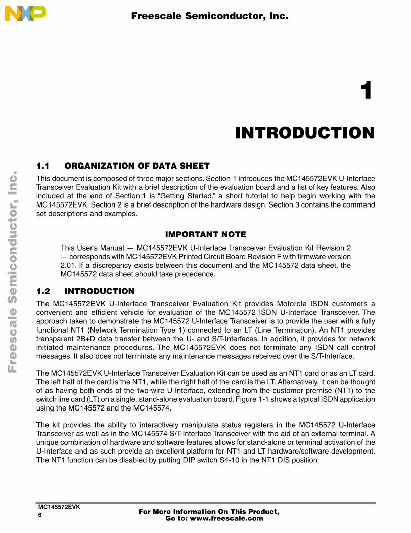
This document is composed of three major sections. Section 1 introduces the MC145572EVK U-InterfaceTransceiver Evaluation Kit with a brief description of the evaluation board and a list of key features. Alsoincluded at the end of Section 1 is ÒGetting Started,Ó a short tutorial to help begin working with theMC145572EVK. Section 2 is a brief description of the hardware design. Section 3 contains the commandset descriptions and examples.
IMPORTANT NOTE
This UserÕs Manual Ñ MC145572EVK U-Interface Transceiver Evaluation Kit Revision 2Ñ corresponds with MC145572EVK Printed Circuit Board Revision F with Þrmware version2.01. If a discrepancy exists between this document and the MC145572 data sheet, theMC145572 data sheet should take precedence.
1.2 INTRODUCTION
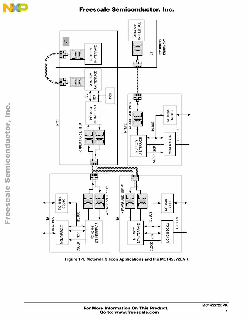
The MC145572EVK U-Interface Transceiver Evaluation Kit provides Motorola ISDN customers aconvenient and efÞcient vehicle for evaluation of the MC145572 ISDN U-Interface Transceiver. Theapproach taken to demonstrate the MC145572 U-Interface Transceiver is to provide the user with a fullyfunctional NT1 (Network Termination Type 1) connected to an LT (Line Termination). An NT1 providestransparent 2B+D data transfer between the U- and S/T-Interfaces. In addition, it provides for networkinitiated maintenance procedures. The MC145572EVK does not terminate any ISDN call controlmessages. It also does not terminate any maintenance messages received over the S/T-Interface.
The MC145572EVK U-Interface Transceiver Evaluation Kit can be used as an NT1 card or as an LT card.The left half of the card is the NT1, while the right half of the card is the LT. Alternatively, it can be thoughtof as having both ends of the two-wire U-Interface, extending from the customer premise (NT1) to theswitch line card (LT) on a single, stand-alone evaluation board. Figure 1-1 shows a typical ISDN applicationusing the MC145572 and the MC145574.
The kit provides the ability to interactively manipulate status registers in the MC145572 U-InterfaceTransceiver as well as in the MC145574 S/T-Interface Transceiver with the aid of an external terminal. Aunique combination of hardware and software features allows for stand-alone or terminal activation of theU-Interface and as such provide an excellent platform for NT1 and LT hardware/software development.The NT1 function can be disabled by putting DIP switch S4-10 in the NT1 DIS position.
Fre
esc
ale
Se
mic
on
du
cto
r, I
Freescale Semiconductor, Inc.
For More Information On This Product, Go to: www.freescale.com
nc
...
7MC145572EVK
Figure 1-1. Motorola Silicon Applications and the MC145572EVK
MC
1455
72U
-INTE
RFA
CE
MC
1455
74S/
T-IN
TER
FAC
E
MC
U
X-FR
MR
S AN
D L
INE
I/F
NT1/
TE1
SWIT
CHIN
G
SCP
CLO
CK M
CM
C68
SC30
2
HO
ST B
US
MC
1454
80C
OD
EC
TA
LT
LT
MC
1455
72U
-INTE
RFA
CE
MC
1455
72U
-INTE
RFA
CE
MC
1455
72U
-INTE
RFA
CE
IDL
IDL
BUS
SCP
X-FR
MR
S AN
D L
INE
I/F
EQUI
PMEN
T
NT1
TA
X-FR
MR
S AN
D L
INE
I/F
IDL
BUS
SCP
HO
ST B
US
MC
1454
80C
OD
EC
MC
1455
74S/
T-IN
TER
FAC
E
MC
1455
74S/
T-IN
TER
FAC
E
CLO
CK
SCP
IDL
BUS
MC
1454
80C
OD
EC
X-FR
MR
S AN
D L
INE
I/F
HO
ST B
US
CLO
CK M
CM
C68
SC30
2
MC
MC
68SC
302
Fre
esc
ale
Se
mic
on
du
cto
r, I
Freescale Semiconductor, Inc.
For More Information On This Product, Go to: www.freescale.com
nc
...
MC145572EVK8
1.3 FEATURES
1.3.1 General
·
Provides Stand-Alone NT1 and LT on Single Board
·
On-Board 68HC05 Microcontroller with Resident Monitor Software
·
Convenient Access to Key Signals
·
NT1 and LT Software Development Platform
1.3.2 Hardware
·
+ 5 V Only Power Supply
·
ÒPush-ButtonÓ Activation of U-Interface from NT1
·
Stand-Alone Operation for Bit Error Rate Testing
·
Gated Data Clocks Provided for Bit Error Rate Testing
·
Can Be Used as a U- or S/T-Interface Terminal Development Tool
·
On-Board 5 ppm LT Frequency Reference
·
EIA-232 (V.28) Serial Port for Terminal Interface
1.3.3 Software
·
Stand-Alone or Terminal Operation
·
Resident Firmware Monitor for User Control of Board
·
Activation and Deactivation Menus
·
Embedded Operations Channel
·
Microcontroller Controlled or Automatic Activation/Deactivation
·
Access to All Maintenance Channels
·
MC68HC05 Assembly Language Source Code Available
Fre
esc
ale
Se
mic
on
du
cto
r, I
Freescale Semiconductor, Inc.
For More Information On This Product, Go to: www.freescale.com
nc
...

9MC145572EVK
1.4 BLOCK DIAGRAM
Following is a basic functional block diagram for the MC145572EVK U-Interface Transceiver EvaluationKit (Figure 1-2). While the board is capable of activating Òstand-alone,Ó the user may decide to use a singleASCII terminal to gain total control of the MC145572EVKÕs activities.
Figure 1-2. MC145572EVK Functional Block Diagram
1.5 GETTING STARTED
This section is provided to facilitate the userÕs introduction to the MC145572EVK. To maximize efÞciencywhen working with the MC145572EVK, it is recommended that the user become familiar with theorganization of this document as well as the MC145572 U-Interface Transceiver data sheet. To identify astarting point, power up the board and activate the U-Interface immediately. The only equipment neededis a 5 V, 250 mA power supply, a two-wire U-Interface cable, and the MC145572EVK.
NOTE
The board shipped from the factory was thoroughly tested and veriÞed to function properlyprior to shipment. If you experience any problems or difÞculties with the operation of theMC145572EVK, do not hesitate to call the factory or your local Motorola representative forassistance.
1. Remove the board from its conductive environment at a static-controlled station.
2. Examine the board and its components to make certain nothing was damaged during shipment ofthe board.
3. Verify that the ICs are seated properly in the socket.
5 ppmCLOCK
SOURCE
REFERENCECLOCK
GENERATOR
MC145572ISDN
U-INTERFACETRANSCEIVER
MC145574ISDN
S/T-INTERFACETRANSCEIVER
MC68HC705MICROCONTROLLER
MC145407GATEDCLOCK
GENERATOR
GATEDCLOCK
GENERATOR
MC145572ISDN
U-INTERFACETRANSCEIVER
IDLIDL
S/T
BERTCLK
NT U-INTERFACE LT U-INTERFACE
EXT CLK
SCP
RS-232
NETWORK TERMINATION LINE TERMINATION
BERTCLK
Fre
esc
ale
Se
mic
on
du
cto
r, I
Freescale Semiconductor, Inc.
For More Information On This Product, Go to: www.freescale.com
nc
...
MC145572EVK10
4. Become familiar with the layout and the various connectors. Locate the power connector J19.Locate the U-Interface connectors, J2 (LT U-Interface side) and J12 (NT U-Interface side).
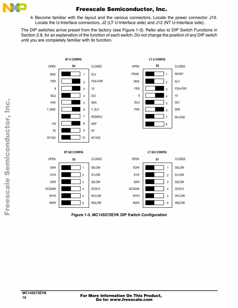
The DIP switches arrive preset from the factory (see Figure 1-3). Refer also to DIP Switch Functions inSection 2.8, for an explanation of the function of each switch. Do not change the position of any DIP switchuntil you are completely familiar with its function.
Figure 1-3. MC145572EVK DIP Switch Configuration
S4
S0HI
S1HI
S2HI
GCI2048
IN1HI
IN2HI
OPEN
S0LOW
S1LOW
S2LOW
GCI512
IN1LOW
IN2LOW
CLOSEDS3
OPEN
MAS
FSR
8
IDL2
PAR
T_MAS
CLOSED
SLV
FSX=FSR
10
GCI
SER
T_SLV
RESMCU
ADP
NT
NT1DIS
FIX
TE
NT1EN
SOHI
S1HI
S2HI
GCI2048
IN1HI
IN2HI
OPEN
S0LOW
S1LOW
S2LOW
GCI512
IN1LOW
IN2LOW
CLOSEDS1
MAS
FSR
8
IDL2
PAR
OPEN S2
FSX=FSR
RF=FSR
SLV
10
GCI
SER
CLOSED
RFOFFFRON
LT U CONFIG
LT GCI CONFIG
NT U CONFIG
NT GCI CONFIG
1
2
3
4
5
6
7
8
9
10
1
2
3
4
5
6
7
8
1
2
3
4
5
6
1
2
3
4
5
6
Fre
esc
ale
Se
mic
on
du
cto
r, I
Freescale Semiconductor, Inc.
For More Information On This Product, Go to: www.freescale.com
nc
...
11MC145572EVK
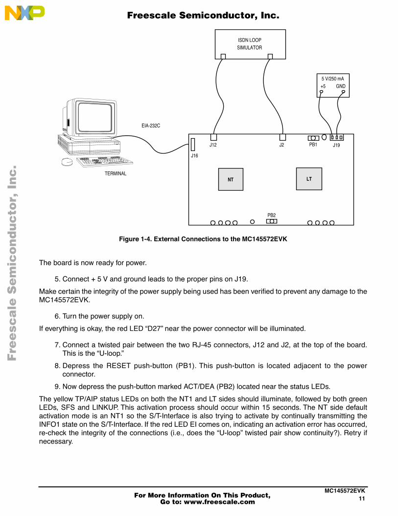
Figure 1-4. External Connections to the MC145572EVK
The board is now ready for power.
5. Connect + 5 V and ground leads to the proper pins on J19.
Make certain the integrity of the power supply being used has been veriÞed to prevent any damage to theMC145572EVK.
6. Turn the power supply on.
If everything is okay, the red LED ÒD27Ó near the power connector will be illuminated.
7. Connect a twisted pair between the two RJ-45 connectors, J12 and J2, at the top of the board.This is the ÒU-loop.Ó
8. Depress the RESET push-button (PB1). This push-button is located adjacent to the powerconnector.
9. Now depress the push-button marked ACT/DEA (PB2) located near the status LEDs.
The yellow TP/AIP status LEDs on both the NT1 and LT sides should illuminate, followed by both greenLEDs, SFS and LINKUP. This activation process should occur within 15 seconds. The NT side defaultactivation mode is an NT1 so the S/T-Interface is also trying to activate by continually transmitting theINFO1 state on the S/T-Interface. If the red LED EI comes on, indicating an activation error has occurred,re-check the integrity of the connections (i.e., does the ÒU-loopÓ twisted pair show continuity?). Retry ifnecessary.
ISDN LOOPSIMULATOR
J12 J2
J16
5 V/250 mA+5 GND
EIA-232C
NT LTTERMINAL
J19PB1
PB2
Fre
esc
ale
Se
mic
on
du
cto
r, I
Freescale Semiconductor, Inc.
For More Information On This Product, Go to: www.freescale.com
nc
...
MC145572EVK12
10. If available, connect an ASCII terminal to J16 (the DB-25 connector on the NT1 side of the board).Make certain the terminal is set for 9600 baud, 1 stop bit, and no parity. If there is no response,reverse the EIA-232 Tx and Rx signals by changing the jumpers on JP13.
11. Depress the RESET push-buttons and verify that the ÒNTLT>Ó prompt has appeared on the terminalscreen.
Continue reading this document to learn more about the operation of the MC145572EVK U-InterfaceTransceiver Evaluation Kit. As always, please phone the factory for assistance with any problemsencountered while ÒGetting Started.Ó
Fre
esc
ale
Se
mic
on
du
cto
r, I
Freescale Semiconductor, Inc.
For More Information On This Product, Go to: www.freescale.com
nc
...
13MC145572EVK
2
HARDWARE REFERENCE
NOTE
Refer to the MC145572EVK Printed Circuit Board and to the MC145572 U-InterfaceTransceiver data sheet to supplement this section. Please contact the factory beforecommitting design to PCB to be guaranteed notiÞcation of any improvements to the followingcircuitry. The schematic of the MC145572EVK is in Appendix A of this manual.
2.1 U-INTERFACE
The U-Interface is implemented with MotorolaÕs single chip MC145572 U-Interface Transceiver (U10 onthe NT1 and U1 on the LT side), providing ISDN Basic Rate Access capability for twisted-pair loops withconformance to ANSI T1.601-1992. For additional speciÞcations on designing with and the operation ofthe MC145572, refer to the MC145572 U-Interface Transceiver data sheet in addition to this document.
2.1.1 Line Interface Circuitry
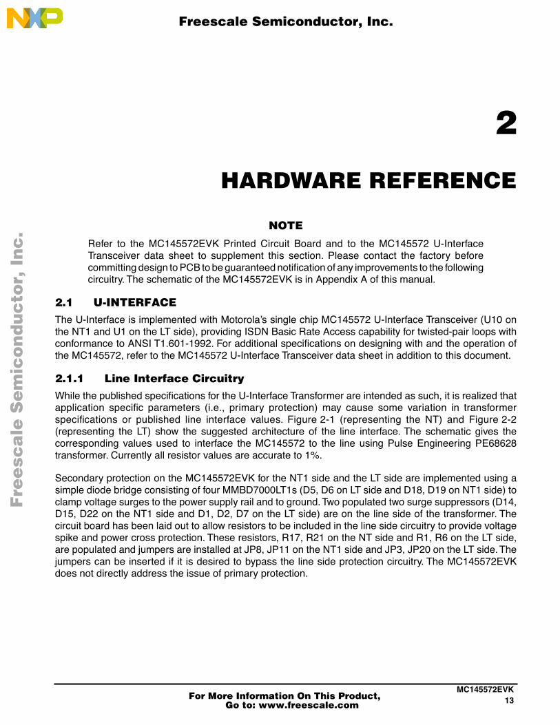
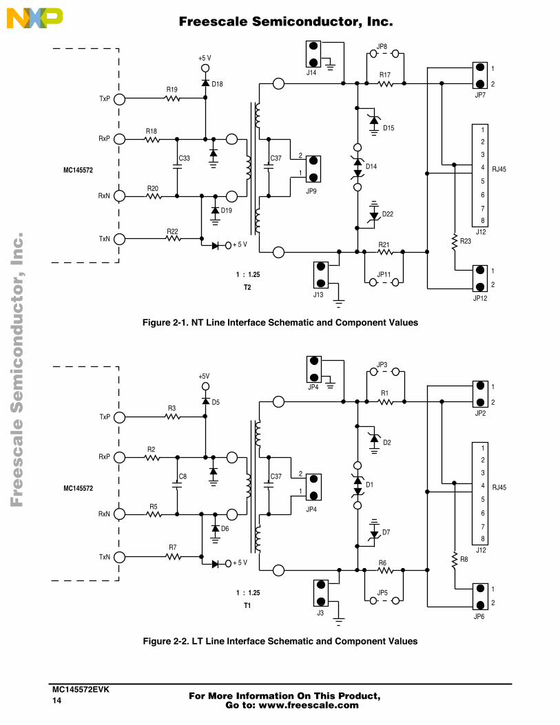
While the published speciÞcations for the U-Interface Transformer are intended as such, it is realized thatapplication speciÞc parameters (i.e., primary protection) may cause some variation in transformerspeciÞcations or published line interface values. Figure 2-1 (representing the NT) and Figure 2-2(representing the LT) show the suggested architecture of the line interface. The schematic gives thecorresponding values used to interface the MC145572 to the line using Pulse Engineering PE68628transformer. Currently all resistor values are accurate to 1%.
Secondary protection on the MC145572EVK for the NT1 side and the LT side are implemented using asimple diode bridge consisting of four MMBD7000LT1s (D5, D6 on LT side and D18, D19 on NT1 side) toclamp voltage surges to the power supply rail and to ground. Two populated two surge suppressors (D14,D15, D22 on the NT1 side and D1, D2, D7 on the LT side) are on the line side of the transformer. Thecircuit board has been laid out to allow resistors to be included in the line side circuitry to provide voltagespike and power cross protection. These resistors, R17, R21 on the NT side and R1, R6 on the LT side,are populated and jumpers are installed at JP8, JP11 on the NT1 side and JP3, JP20 on the LT side. Thejumpers can be inserted if it is desired to bypass the line side protection circuitry. The MC145572EVKdoes not directly address the issue of primary protection.
Fre
esc
ale
Se
mic
on
du
cto
r, I
Freescale Semiconductor, Inc.
For More Information On This Product, Go to: www.freescale.com
nc
...
MC145572EVK14
Figure 2-1. NT Line Interface Schematic and Component Values
Figure 2-2. LT Line Interface Schematic and Component Values
TxP
TxN
RxP
RxN
C37
MC145572
1 : 1.25
R19
R22
C33
+5 V
D18
D19
+ 5 V
2
1
JP9
R17
R21
D15
D22
D14
JP11
JP8
J12
RJ45
T2
R18
R20
2
1
JP12
2
1
JP7
R23
J13
3
5
6
8
7
4
2
1
J14
TxP
TxN
RxP
RxN
C37
MC145572
1 : 1.25
R3
R7
C8
+5V
D5
D6
+ 5 V
2
1
JP4
R1
R6
D2
D7
D1
JP5
JP3
J12
RJ45
T1
R2
R5
2
1
JP6
2
1
JP2
R8
J3
3
5
6
8
7
4
2
1
JP4
Fre
esc
ale
Se
mic
on
du
cto
r, I
Freescale Semiconductor, Inc.
For More Information On This Product, Go to: www.freescale.com
nc
...
15MC145572EVK
2.1.2 Crystal Oscillator (LT Mode)
In the LT mode, the internal phase locked loop (PLL) of the MC145572 generates a 20.48 MHz clock whichis phase locked to an 8 kHz reference clock applied at the FREQREF pin. This assures that the transmitted2B1Q signal is synchronized to the 8 kHz frequency reference. A single pullable crystal, Y1, is all that isrequired for the MC145572 oscillator. All other frequency pulling circuitry is internal to the MC145572.
It is also possible to provide an external 8 kHz frequency reference rather than using the 8 kHz frequencyreference generated on-board from the 5 ppm oscillator, Y5. This is accomplished using the RF
off
-RF
on
switch of S2-1 and connecting the external reference to EXTREF of J9. RF
off
selects the off-board 8 kHzfrequency reference and RF
on
selects the on-board 8 kHz frequency reference. See also the explanationfor S2-1 and S2-7 in Section 2.7.2.
2.1.3 Crystal Oscillator (NT Mode)
The NT-conÞgured MC145572 U10, requires only a single pullable crystal, Y2, for its oscillator. All otherfrequency pulling circuitry is internal to the MC145572.
2.2 S/T-INTERFACE
The S/T-Interface resides on the NT1 portion of the MC145572EVK and is implemented using theMC145574 S/T-Interface Transceiver (U17). The 600 mil 28-pin Plastic SOIC MC145574 conforms to bothCCITT I.430 and ANSI T1.605 speciÞcations. External line interface circuitry for switching between NTand TE operating modes is incorporated.
Two 8-pin RJ-45 telephone jacks are used at the S/T-Interface, one conÞgured for the NT mode (J24) ofoperation and one conÞgured for the TE mode (J23) of operation. The Tx pair, pins 4 and 5 on the NT jackand pins 3 and 6 on the TE jack, are driven by the TxP and TxN pins which act as a current limited differentialvoltage source. The drive resistance (R40, R42) is necessary to conform to the ANSI T1.605 pulse maskspeciÞcation. A dual 2.5:1 turns ratio transformer (T4A:B) is used to couple the Tx and Rx pairs to the4-wire interface. A high frequency 4-wire common mode choke transformer (T3 for TE and T5 for NT)provides an effective means of compliance with EMI suppression.
The protection diodes (D29A:G, D30A:G MMAD1108) provide secondary protection to the MC145574,even when it is powered down, without loading the S/T-Interface bus. CCITT I.430, ETSI ETS 300012, andANSI T1.605 specify that the S/T-interface voltage cannot exceed 1.6 times the nominal voltage of 750 mV(= 1.2 V). Since the MC145574 is designed to operate with 2.5:1 turns ratio transformers, the diode structureis required to provide protection, while not adversely affecting the S/T-interface when power is removedfrom the device. This diode structure also protects the circuit against electrostatic discharges (ESD) andlatch-up.
The S/T-Interface Transceiver implementation on this board can be used in either NT or TE mode. Pin 4,TE/NT(L), of the MC145574 determines whether the chip is in NT or TE mode of operation. WhenconÞgured as a TE, pins 9 and 8 are used as DREQUEST and DGRANT, respectively. The DREQUESTpin is used by an external controller such as the MC145488 DDLC or the MC68302 IMP to request accessto the D-Channel. When the S/T-Interface Transceiver gains access to the D-Channel time slot on theS/T-Interface bus, it asserts DGRANT high, informing the external controller that it can transmit itsD-Channel data in the next IDL D time slot. In the NT mode, pin 6 performs the FIX and TFSC functions.FIX tells the S/T-Interface Transceiver to use Fixed or Adaptive timing recovery. TFSC is asserted whenframe synchronization has been achieved at the S/T-Interface bus. For a more complete discussion onD-Channel operation, please refer to Section 11 of the MC145574/75 S/T-Interface Transceiver datamanual.
With the left side of the board operating as an NT1, the MC145574 S/T-Interface Transceiver is in the NTmode, operating as an IDL Slave, and is receiving its Clock and Sync signals from the MC145572
Fre
esc
ale
Se
mic
on
du
cto
r, I
Freescale Semiconductor, Inc.
For More Information On This Product, Go to: www.freescale.com
nc
...
MC145572EVK16
U-Interface Transceiver. Access to the control registers within the S/T-Interface Transceiver is gainedthrough the SCP Interface. The registers are displayed and changed via resident software on theMC145572EVK. A complete description of the S/T-Interface Transceiver registers can be found in Sections8, 9, and 10 of the MC145574 S/T-Interface Transceiver data sheet.
2.3 MICROCONTROLLERS
The MC145572EVK is an MC68HC705C8 microcontroller-based system. One microcontroller resides onthe board; U15 on the NT1 side which controls both the NT1 and the LT sides. The hardware RESETpush-button is located next to the power supply connection for the microcontroller. U5 must be populatedfor the display LEDs to operate properly.
The U-Interface may be activated using an ASCII terminal connected to the EIA-232 (V.28) port markedJ16 on the NT1 side. The board may be activated as it Òstands aloneÓ with the push of a button. The defaultactivation mode for the Activate/Deactivate push-button, PB2 (located near the front of the board), is asan NT1, with INFO1 continually transmitted on the S/T-Interface until it receives INFO2. When DIP switchS4-10 is in the NT1DIS position, the NT1 functionality is disabled. The LT side initiates activation on theU-Interface. Eight status LEDs (D10, D11, D12, and D13 on LT side and D23, D24, D25, and D26 on theNT1 side) are continuously updated by the MC68HC705C8s to provide the user with a visual update ofthe U-Interface activation status.
When the MC145572EVK is reset, it defaults to NT1 function enabled and automatic handling of M4maintenance channel on the LT side U-transceiver. The NT1 function can also be disabled by entering theÒNOFÓ command. The LT maintenance can be disabled by entering the ÒLOFÓ command. See Section 3.2for more information on LOF, LON, NOF, and NON commands.
2.3.1 Status LEDs
Ten status LEDs are provided on the MC145572EVK to offer the user a quick visual update to criticalstatus parameters.
One red LED, D27 on the LT, is located near the power connector and is illuminated when + 5 V is appliedto the board.
One green LED (D31) marked S/T ACT located near the PB2 (ACT/DEA) push button, illuminates toindicate that the MC145574 when conÞgured as an NT has achieved frame synchronization.
Located on both sides of the board are four LEDs representing Nibble Register 1 (NR1) of each U-InterfaceTransceiver. The LEDs in each bank are each marked with LINKUP, EI, SFS, and TP/AIP. They map directlyto the register contents as shown below.
NOTE
The received data is not transmitted on the IDL2 Interface until Linkup is a 1, SFS is a 1,TP/AIP is a 1, and either CustEn (see NR2 in MC145572 U-Interface Transceiver datasheet) or VerifAct is a 1 (see BR9 in MC145572 U-Interface Transceiver data sheet).
b3 b2 b1 b0
NR1
Linkup Error Indication Superframe Sync Transparent/Activation in Progress
NT (LED Silkscreen)
NT LINKUP NT EI NT SFS NT TP/AIP
LT (LED Silkscreen)
LT LINKUP LT EI LT SFS LT TP/AIP
Fre
esc
ale
Se
mic
on
du
cto
r, I
Freescale Semiconductor, Inc.
For More Information On This Product, Go to: www.freescale.com
nc
...
17MC145572EVK
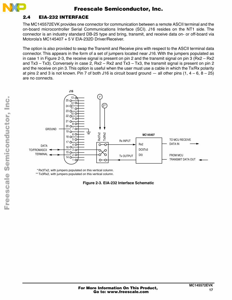
2.4 EIA-232 INTERFACE
The MC145572EVK provides one connector for communication between a remote ASCII terminal and theon-board microcontroller Serial Communications Interface (SCI). J16 resides on the NT1 side. Theconnector is an industry standard DB-25 type and bring, transmit, and receive data on- or off-board viaMotorolaÕs MC145407 + 5 V EIA-232D Driver/Receiver.
The option is also provided to swap the Transmit and Receive pins with respect to the ASCII terminal dataconnector. This appears in the form of a set of jumpers located near J16. With the jumpers populated asin case 1 in Figure 2-3, the receive signal is present on pin 2 and the transmit signal on pin 3 (Rx2 Ð Rx2and Tx3 Ð Tx3). Conversely in case 2, Rx2 Ð Rx2 and Tx3 Ð Tx3, the transmit signal is present on pin 2and the receive on pin 3. This option is useful when the user must use a cable in which the Tx/Rx polarityat pins 2 and 3 is not known. Pin 7 of both J16 is circuit board ground Ñ all other pins (1, 4 Ð 6, 8 Ð 25)are no connects.
Figure 2-3. EIA-232 Interface Schematic
1
2
3
4
5
6
7
8
9
10
11
12
13
14
15
16
17
18
19
20
21
22
23
24
25
Rx2
DO3Tx3
DI3
MC145407
1*
2**
Rx INPUT
Tx OUTPUT
TO MCU RECEIVE DATA IN
FROM MCU TRANSMIT DATA OUT
GROUND
DATA TO/FROMASCII
TERMINAL
Rx3
Tx2
Tx3R
x2
J16
* Rx3Tx2, with jumpers populated on this vertical column.** Tx3Rx2, with jumpers populated on this vertical column.
Fre
esc
ale
Se
mic
on
du
cto
r, I
Freescale Semiconductor, Inc.
For More Information On This Product, Go to: www.freescale.com
nc
...
MC145572EVK18
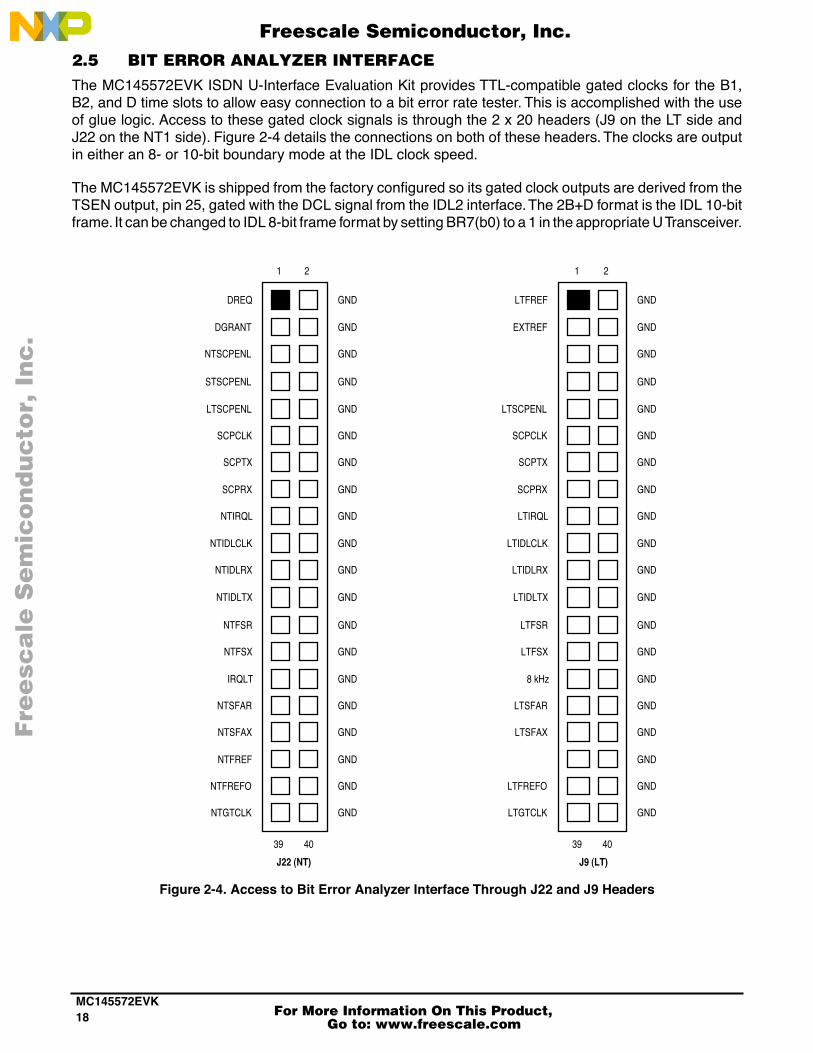
2.5 BIT ERROR ANALYZER INTERFACE
The MC145572EVK ISDN U-Interface Evaluation Kit provides TTL-compatible gated clocks for the B1,B2, and D time slots to allow easy connection to a bit error rate tester. This is accomplished with the useof glue logic. Access to these gated clock signals is through the 2 x 20 headers (J9 on the LT side andJ22 on the NT1 side). Figure 2-4 details the connections on both of these headers. The clocks are outputin either an 8- or 10-bit boundary mode at the IDL clock speed.
The MC145572EVK is shipped from the factory conÞgured so its gated clock outputs are derived from theTSEN output, pin 25, gated with the DCL signal from the IDL2 interface. The 2B+D format is the IDL 10-bitframe. It can be changed to IDL 8-bit frame format by setting BR7(b0) to a 1 in the appropriate U Transceiver.
Figure 2-4. Access to Bit Error Analyzer Interface Through J22 and J9 Headers
1 2
4039
DREQ
DGRANT
NTSCPENL
STSCPENL
LTSCPENL
SCPCLK
SCPTX
NTIRQL
NTIDLCLK
NTIDLRX
NTIDLTX
NTFSR
NTFSX
IRQLT
NTSFAR
NTSFAX
NTFREF
NTFREFO
NTGTCLK
SCPRX
GND
GND
GND
GND
GND
GND
GND
GND
GND
GND
GND
GND
GND
GND
GND
GND
GND
GND
GND
GND
J22 (NT)
1 2
4039
LTFREF
EXTREF
LTSCPENL
SCPCLK
SCPTX
LTIRQL
LTIDLCLK
LTIDLRX
LTIDLTX
LTFSR
LTFSX
8 kHz
LTSFAR
LTSFAX
LTFREFO
LTGTCLK
SCPRX
GND
GND
GND
GND
GND
GND
GND
GND
GND
GND
GND
GND
GND
GND
GND
GND
GND
GND
GND
GND
J9 (LT)
Fre
esc
ale
Se
mic
on
du
cto
r, I
Freescale Semiconductor, Inc.
For More Information On This Product, Go to: www.freescale.com
nc
...
19MC145572EVK
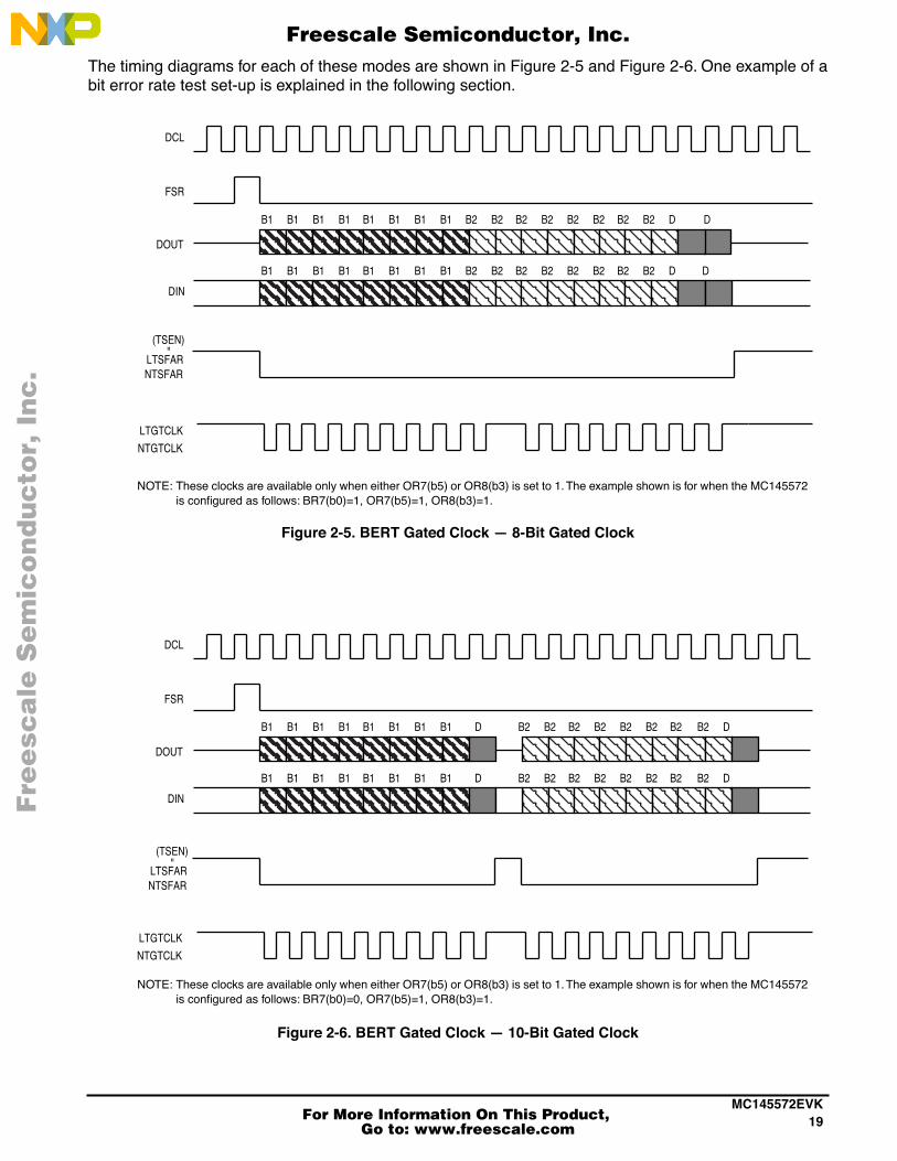
The timing diagrams for each of these modes are shown in Figure 2-5 and Figure 2-6. One example of abit error rate test set-up is explained in the following section.
Figure 2-5. BERT Gated Clock Ñ 8-Bit Gated Clock
Figure 2-6. BERT Gated Clock Ñ 10-Bit Gated Clock
DOUT
B1 B1 B1 B1 B1 B1 B1 B1 DB2 B2 B2 B2 B2 B2 B2 B2 D
B1 B1 B1 B1 B1 B1 B1 B1 DB2 B2 B2 B2 B2 B2 B2 B2 D
DIN
FSR
DCL
LTGTCLK
NTGTCLK
(TSEN)
NTSFAR
NOTE: These clocks are available only when either OR7(b5) or OR8(b3) is set to 1. The example shown is for when the MC145572is conÞgured as follows: BR7(b0)=1, OR7(b5)=1, OR8(b3)=1.
LTSFAR"
DOUT
B1 B1 B1 B1 B1 B1 B1 B1 D B2 B2 B2 B2 B2 B2 B2 B2 D
B1 B1 B1 B1 B1 B1 B1 B1 D B2 B2 B2 B2 B2 B2 B2 B2 D
DIN
FSR
DCL
LTGTCLK
NTGTCLK
NOTE: These clocks are available only when either OR7(b5) or OR8(b3) is set to 1. The example shown is for when the MC145572is conÞgured as follows: BR7(b0)=0, OR7(b5)=1, OR8(b3)=1.
(TSEN)
NTSFARLTSFAR
"
Fre
esc
ale
Se
mic
on
du
cto
r, I
Freescale Semiconductor, Inc.
For More Information On This Product, Go to: www.freescale.com
nc
...
MC145572EVK20
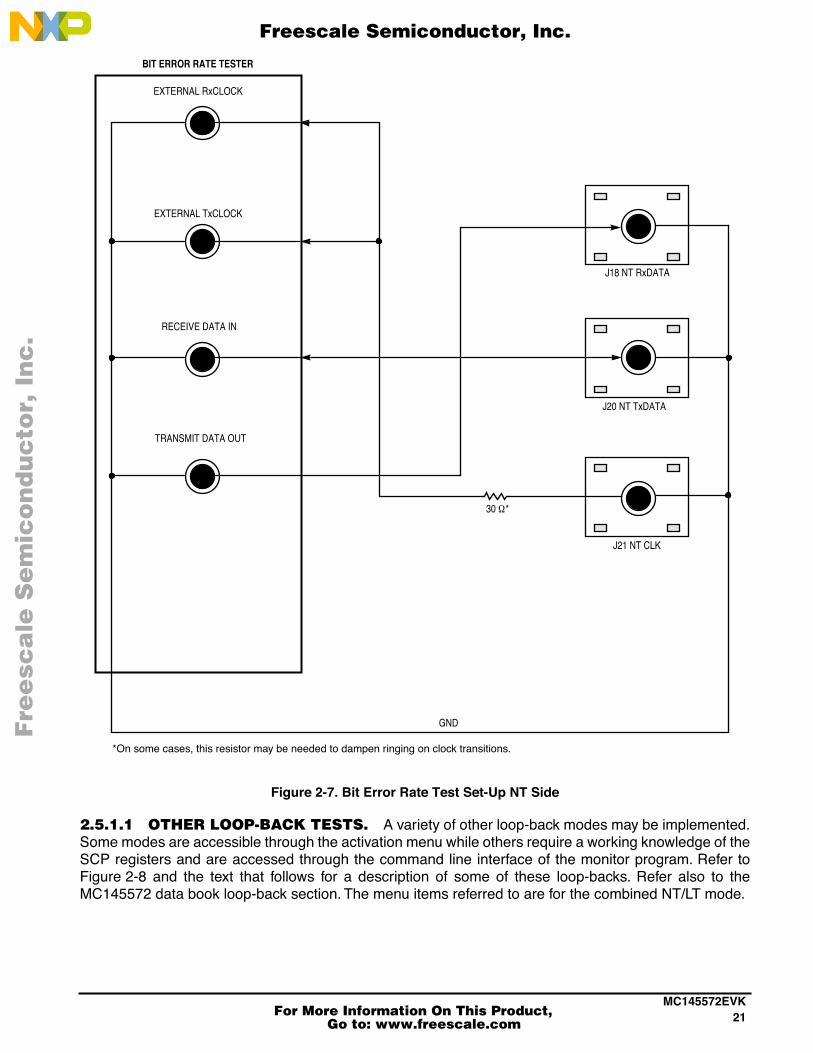
2.5.1 Setting Up a Bit Error Rate Test
Bit error rate testing with two different testers has been performed. The Hewlett Packard 1645A Data ErrorAnalyzer and The Telecommunications Techniques Corporation FIREBERD 6000 with Lab InterfaceAdapter have successfully been connected to the MC145572EVK. Any bit error test that accepts TTL levelsignals and external data clocks up to 2.56 MHz at TTL levels may be used. The clock interface supportssynchronous clocked data through the use of gated clocks running at IDL rates of 512 kHz, 2.048 MHz,or 2.56 MHz, as determined by register BR7(b2) and OR7(b4) of the U-Interface Transceiver.
CAUTION
The MC145572EVK does not support EIA-232, RS-422, 50W, or RS-485 interfaces to biterror rate testers.
To demonstrate the connection of the MC145572EVK U-Interface Transceiver Evaluation Kit to a bit errorrate tester, detailed instructions for one test set-up follows.
EXAMPLE: Executing a 2B+D Loop-Back to the U-Interface at the LT End.
This example shows how to connect a bit error rate tester to the MC145572EVK. Refer to Figure 2-7 forconnection details.
The data ßow for this example occurs as follows: data is input to the board by the BERT box on NTRXDATAat the NT1. This data is then input to the MC145572 where it is framed, coded, and transmitted over theU-Interface to the LT MC145572, and looped-back internal to the LT MC145572. The data is thentransmitted back to the NT MC145572 over the U-Interface, decoded, deframed, and output from the NTMC145572 on NTTXDATA to the BERT box where it is compared to the data originally transmitted.
1. Make the following connections to the Bit Error Rate Tester as shown in Figure 2-7.
a. Connect NTTXDATA (BNC J20, Dout pin of the NT U-Interface Transceiver) to the ReceiveData Input of the BERT box.
b. Connect NTRXDATA (BNC JP18, Din pin of the NT U-Interface Transceiver) to the TransmitData Output of the BERT box.
c. Connect NTCLK (BNC J21, gated clock output for the B1+B2+D time slot) to the ExternalTransmit and External Receive Clock inputs of the BERT box.
2. Verify that the DIP switches are set as in Figure 1-3 (valid for above-mentioned BERT boxes).
3. ConÞgure the bit error rate tester to transmit data on the rising edge of the data clock and receivedata on the falling edge of the data clock.
4. Using an ASCII terminal connected to J16, activate the MC145572EVK using the activation menuitem J. Activate both U chips, 2B+D loop back to U-Interface at LT end, disable S/T chip.
5. Begin bit error rate testing when status LEDs indicate loop is successfully activated.
Fre
esc
ale
Se
mic
on
du
cto
r, I
Freescale Semiconductor, Inc.
For More Information On This Product, Go to: www.freescale.com
nc
...
21MC145572EVK
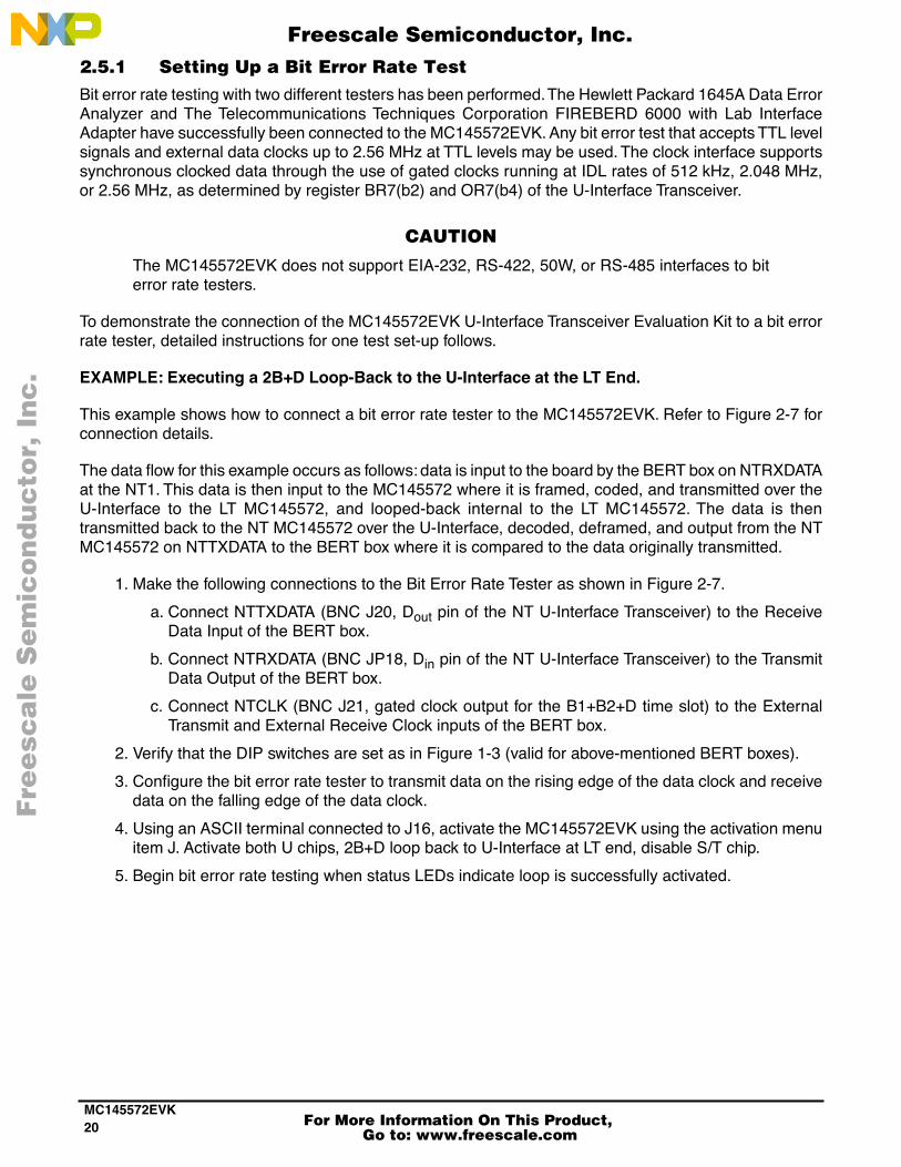
Figure 2-7. Bit Error Rate Test Set-Up NT Side
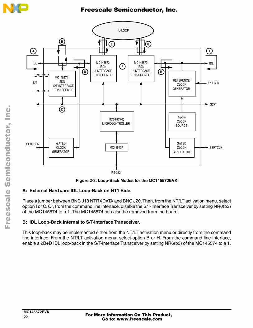
2.5.1.1 OTHER LOOP-BACK TESTS. A variety of other loop-back modes may be implemented.Some modes are accessible through the activation menu while others require a working knowledge of theSCP registers and are accessed through the command line interface of the monitor program. Refer toFigure 2-8 and the text that follows for a description of some of these loop-backs. Refer also to theMC145572 data book loop-back section. The menu items referred to are for the combined NT/LT mode.
J18 NT RxDATA
J20 NT TxDATA
J21 NT CLK
30 W*
GND
BIT ERROR RATE TESTER
EXTERNAL RxCLOCK
EXTERNAL TxCLOCK
RECEIVE DATA IN
TRANSMIT DATA OUT
*On some cases, this resistor may be needed to dampen ringing on clock transitions.
Fre
esc
ale
Se
mic
on
du
cto
r, I
Freescale Semiconductor, Inc.
For More Information On This Product, Go to: www.freescale.com
nc
...
MC145572EVK22
Figure 2-8. Loop-Back Modes for the MC145572EVK
A: External Hardware IDL Loop-Back on NT1 Side.
Place a jumper between BNC J18 NTRXDATA and BNC J20. Then, from the NT/LT activation menu, selectoption I or C. Or, from the command line interface, disable the S/T-Interface Transceiver by setting NR0(b3)of the MC145574 to a 1. The MC145574 can also be removed from the board.
B: IDL Loop-Back Internal to S/T-Interface Transceiver.
This loop-back may be implemented either from the NT/LT activation menu or directly from the commandline interface. From the NT/LT activation menu, select option B or H. From the command line interface,enable a 2B+D IDL loop-back in the S/T-Interface Transceiver by setting NR6(b3) of the MC145574 to a 1.
5 ppmCLOCK
SOURCE
REFERENCECLOCK
GENERATOR
MC145572ISDN
U-INTERFACETRANSCEIVER
MC145574ISDN
S/T-INTERFACETRANSCEIVER
MC68HC705MICROCONTROLLER
MC145407GATEDCLOCK
GENERATOR
GATEDCLOCK
GENERATOR
MC145572ISDN
U-INTERFACETRANSCEIVER
IDLIDL
S/T
BERTCLK
U-LOOP
EXT CLK
SCP
RS-232
BERTCLK
A
B
D
E G
F
H
I
C
Fre
esc
ale
Se
mic
on
du
cto
r, I
Freescale Semiconductor, Inc.
For More Information On This Product, Go to: www.freescale.com
nc
...
23MC145572EVK
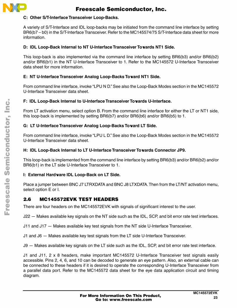
C: Other S/T-Interface Transceiver Loop-Backs.
A variety of S/T-Interface and IDL loop-backs may be initiated from the command line interface by settingBR6(b7 Ð b0) in the S/T-Interface Transceiver. Refer to the MC145574/75 S/T-Interface data sheet for moreinformation.
D: IDL Loop-Back Internal to NT U-Interface Transceiver Towards NT1 Side.
This loop-back is also implemented via the command line interface by setting BR6(b3) and/or BR6(b2)and/or BR6(b1) in the NT U-Interface Transceiver to 1. Refer to the MC145572 U-Interface Transceiverdata sheet for more information.
E: NT U-Interface Transceiver Analog Loop-Backs Toward NT1 Side.
From command line interface, invoke ÒLPU N D.Ó See also the Loop-Back Modes section in the MC145572U-Interface Transceiver data sheet.
F: IDL Loop-Back Internal to U-Interface Transceiver Towards U-Interface.
From LT activation menu, select option B. From the command line interface for either the LT or NT1 side,this loop-back is implemented by setting BR6(b7) and/or BR6(b6) and/or BR6(b5) to 1.
G: LT U-Interface Transceiver Analog Loop-Backs Toward LT Side.
From command line interface, invoke ÒLPU L D.Ó See also the Loop-Back Modes section in the MC145572U-Interface Transceiver data sheet.
H: IDL Loop-Back Internal to LT U-Interface Transceiver Towards Connector JP9.
This loop-back is implemented from the command line interface by setting BR6(b3) and/or BR6(b2) and/orBR6(b1) in the LT side U-Interface Transceiver to 1.
I: External Hardware IDL Loop-Back on LT Side.
Place a jumper between BNC J7 LTRXDATA and BNC J8 LTXDATA. Then from the LT/NT activation menu,select option E or I.
2.6 MC145572EVK TEST HEADERSThere are four headers on the MC145572EVK with signals of signiÞcant interest to the user.
J22 Ñ Makes available key signals on the NT side such as the IDL, SCP, and bit error rate test interfaces.
J11 and J17 Ñ Makes available key test signals from the NT side U-Interface Transceiver.
J1 and J6 Ñ Makes available key test signals from the LT side U-Interface Transceiver.
J9 Ñ Makes available key signals on the LT side such as the IDL, SCP, and bit error rate test interface.
J1 and J11, 2 x 8 headers, make important MC145572 U-Interface Transceiver test signals easilyaccessible. Pins 2, 4, 6, and 10 can be decoded to generate an eye pattern. Also, an external cable canbe connected to these headers if it is desired to operate the corresponding U-Interface Transceiver froma parallel data port. Refer to the MC145572 data sheet for the eye data application circuit and timingdiagram.
Fre
esc
ale
Se
mic
on
du
cto
r, I
Freescale Semiconductor, Inc.
For More Information On This Product, Go to: www.freescale.com
nc
...
MC145572EVK24
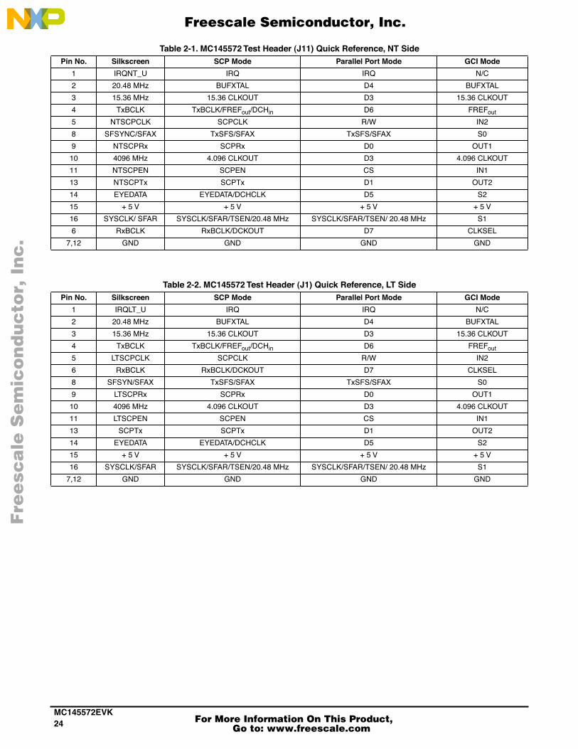
Table 2-1. MC145572 Test Header (J11) Quick Reference, NT SidePin No. Silkscreen SCP Mode Parallel Port Mode GCI Mode
1 IRQNT_U IRQ IRQ N/C
2 20.48 MHz BUFXTAL D4 BUFXTAL
3 15.36 MHz 15.36 CLKOUT D3 15.36 CLKOUT
4 TxBCLK TxBCLK/FREFout/DCHin D6 FREFout
5 NTSCPCLK SCPCLK R/W IN2
8 SFSYNC/SFAX TxSFS/SFAX TxSFS/SFAX S0
9 NTSCPRx SCPRx D0 OUT1
10 4096 MHz 4.096 CLKOUT D3 4.096 CLKOUT
11 NTSCPEN SCPEN CS IN1
13 NTSCPTx SCPTx D1 OUT2
14 EYEDATA EYEDATA/DCHCLK D5 S2
15 + 5 V + 5 V + 5 V + 5 V
16 SYSCLK/ SFAR SYSCLK/SFAR/TSEN/20.48 MHz SYSCLK/SFAR/TSEN/ 20.48 MHz S1
6 RxBCLK RxBCLK/DCKOUT D7 CLKSEL
7,12 GND GND GND GND
Table 2-2. MC145572 Test Header (J1) Quick Reference, LT SidePin No. Silkscreen SCP Mode Parallel Port Mode GCI Mode
1 IRQLT_U IRQ IRQ N/C
2 20.48 MHz BUFXTAL D4 BUFXTAL
3 15.36 MHz 15.36 CLKOUT D3 15.36 CLKOUT
4 TxBCLK TxBCLK/FREFout/DCHin D6 FREFout
5 LTSCPCLK SCPCLK R/W IN2
6 RxBCLK RxBCLK/DCKOUT D7 CLKSEL
8 SFSYN/SFAX TxSFS/SFAX TxSFS/SFAX S0
9 LTSCPRx SCPRx D0 OUT1
10 4096 MHz 4.096 CLKOUT D3 4.096 CLKOUT
11 LTSCPEN SCPEN CS IN1
13 SCPTx SCPTx D1 OUT2
14 EYEDATA EYEDATA/DCHCLK D5 S2
15 + 5 V + 5 V + 5 V + 5 V
16 SYSCLK/SFAR SYSCLK/SFAR/TSEN/20.48 MHz SYSCLK/SFAR/TSEN/ 20.48 MHz S1
7,12 GND GND GND GND
Fre
esc
ale
Se
mic
on
du
cto
r, I
Freescale Semiconductor, Inc.
For More Information On This Product, Go to: www.freescale.com
nc
...
25MC145572EVK
NOTE 1
NTIDLRx is connected to IDLTx pin of the MC145574 S/T-Transceiver. If it is desired for anexternal device to receive IDL data from the MC145574, the signal ÒNTIDLRxÓ must beconnected to the IDL receive input of the external device.
NOTE 2
NTIDLTx is connected to IDLRx pin of the MC145574 S/T-Transceiver. If it is desired for anexternal device to receive IDL data from the MC145574, the signal ÒNTIDLTxÓ must beconnected to the IDL receive input of the external device.
2.6.1 NT Signal Header (JP7) Pin Descriptions
DREQ: S/T-Interface Transceiver DREQUEST.
In the TE mode, this signal is used to indicate to the MC145574 that an external device wishes to transmita layer 2 frame to the NT on the D-channel. Refer to the MC145574 ISDN S/T-Interface Transceiver datasheet.
DGRANT: S/T-Interface Transceiver DGRANT.
In the TE mode, DGRANT operates as a D-channel grant or clear indication. Refer to the MC145574 ISDNS/T-Interface Transceiver data sheet.
NTSCPEN: SCP Enable (NT U-Interface Transceiver SCP EN).
This signal, when held low, selects the Serial Control Port (SCP) for the transfer of control, status, anddata information into and out of the MC145572 U-Interface Transceiver on the NT1 side (U17).
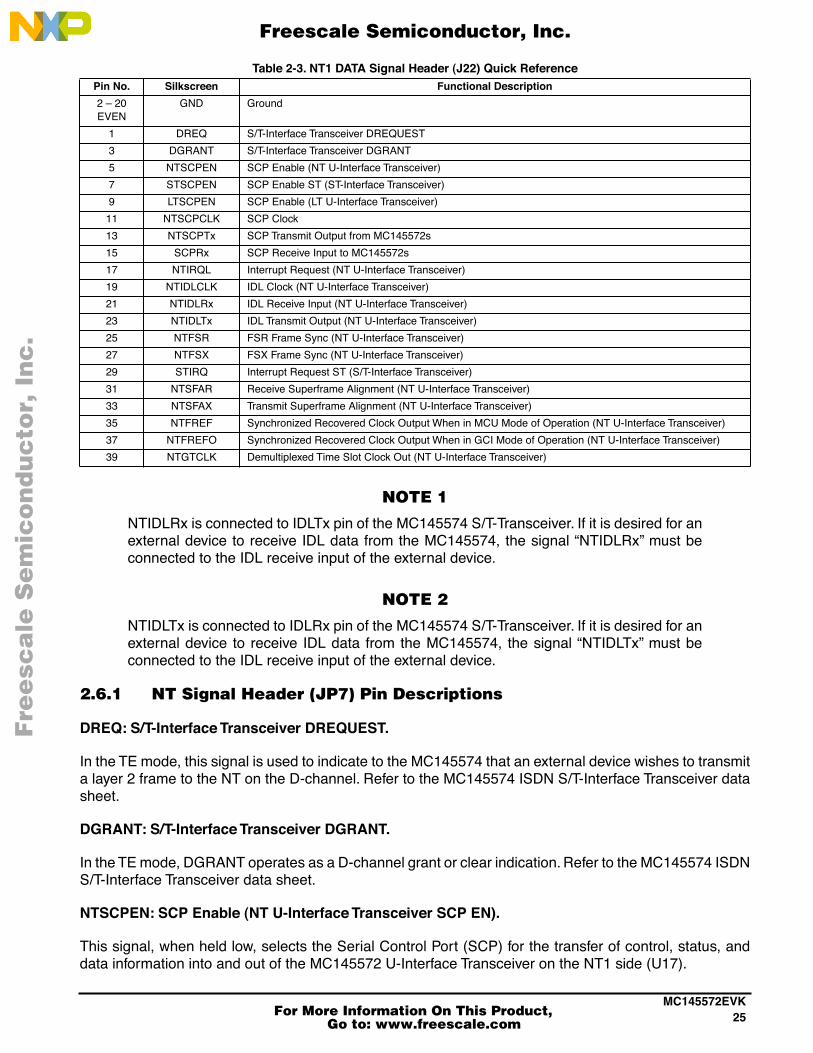
Table 2-3. NT1 DATA Signal Header (J22) Quick ReferencePin No. Silkscreen Functional Description
2 Ð 20 EVEN
GND Ground
1 DREQ S/T-Interface Transceiver DREQUEST
3 DGRANT S/T-Interface Transceiver DGRANT
5 NTSCPEN SCP Enable (NT U-Interface Transceiver)
7 STSCPEN SCP Enable ST (ST-Interface Transceiver)
9 LTSCPEN SCP Enable (LT U-Interface Transceiver)
11 NTSCPCLK SCP Clock
13 NTSCPTx SCP Transmit Output from MC145572s
15 SCPRx SCP Receive Input to MC145572s
17 NTIRQL Interrupt Request (NT U-Interface Transceiver)
19 NTIDLCLK IDL Clock (NT U-Interface Transceiver)
21 NTIDLRx IDL Receive Input (NT U-Interface Transceiver)
23 NTIDLTx IDL Transmit Output (NT U-Interface Transceiver)
25 NTFSR FSR Frame Sync (NT U-Interface Transceiver)
27 NTFSX FSX Frame Sync (NT U-Interface Transceiver)
29 STIRQ Interrupt Request ST (S/T-Interface Transceiver)
31 NTSFAR Receive Superframe Alignment (NT U-Interface Transceiver)
33 NTSFAX Transmit Superframe Alignment (NT U-Interface Transceiver)
35 NTFREF Synchronized Recovered Clock Output When in MCU Mode of Operation (NT U-Interface Transceiver)
37 NTFREFO Synchronized Recovered Clock Output When in GCI Mode of Operation (NT U-Interface Transceiver)
39 NTGTCLK Demultiplexed Time Slot Clock Out (NT U-Interface Transceiver)
Fre
esc
ale
Se
mic
on
du
cto
r, I
Freescale Semiconductor, Inc.
For More Information On This Product, Go to: www.freescale.com
nc
...
MC145572EVK26
STSCPEN: SCP Enable ST (S/T-Interface Transceiver SCP EN).
This signal, when held low, selects the Serial Control Port (SCP) for the transfer of control, status, anddata information into and out of the MC145574 S/T-Interface Transceiver (U17).
LTSCPEN: SCP Enable (LT U-Interface Transceiver SCP EN).
This signal, when held low, selects the Serial Control Port (SCP) for the transfer of control, status, anddata information into and out of the MC145572 U-Interface Transceiver on the LT side (U1). NOTE: Thereis no corresponding interrupt line from U1 to the microcontroller on the NT side of the board.
SCPCLK: SCP Clock (SCP CLK).
SCPCLK is used for controlling the transfer of data into and out of the SCP registers of the U17 S/T chip.Data is shifted into the devices from SCPRx on rising edges of SCPCLK. Data is shifted out of the deviceson SCPTx on falling edges of SCPCLK. SCPCLK can be any frequency up to 4.096 MHz.
SCPTx: SCP Transmit Output (SCP Tx).
SCPTx is used to output control, status, and data information from the two MC145572 U-InterfaceTransceivers and the MC145574 S/T-Interface Transceiver.
SCPRx: SCP Receive Input (SCP Rx).
SCPRx is used to input control, status, and data information to the two MC145572 U-Interface Transceiversand the MC145574 S/T-Interface Transceiver.
NTIRQ: Interrupt Request 1 (NT U-Interface Transceiver IRQ).
The IRQL1 pin is an active low open drain output used to signal the MCU devices that an interrupt conditionexists in the NT1 MC145572 U-Interface Transceiver (U10). On clearing the interrupt condition, the NTIRQpin is returned to the high state.
NTIDLCLK: (NT U-Interface Transceiver Pin DCL).
This pin is an input when the MC145572 is in slave mode and an output when the MC145572 is in mastermode, as established by switch S4-1, MAS/SLV. As a timing master in NT mode, this pin provides a 512 kHz,2.048 MHz, or a 2.56 MHz clock frequency. In GCI mode the 2.56 MHz clock is not available. In GCI modeS1-4, GCI2048/GCI512 selects the clock rate on this pin. In slave mode this pin accepts any clock frequencyfrom 512 kHz to 8.192 MHz, inclusive.
NTIDLRx: (NT U-Interface Transceiver Pin Din).
This pin is the input for the 2B+D data to be transmitted onto the NT1 U-Interface. Data bits are input onsequential falling edges of the NTIDLCLK signal beginning immediately after the FSX pulse occurs. TheNTIDLRx pin is a donÕt care except during valid B- and D-channel data positions. Note that the M and theA bits used in the IDL Interface of the MC145574 S/T-Interface Transceiver are not used by the MC145572,and, therefore, are not received by the MC145572.
NTIDLTx: (NT U-Interface Transceiver Pin Dout).
This pin is the output for the 2B+D data received at the NT1 U-Interface. Data bits are output on risingedges of the IDL CLK signal beginning immediately after the FSR pulse occurs. The NTIDLTx signalremains in a high impedance state when not outputting 2B+D data or when a valid FSR signal is missing.
Fre
esc
ale
Se
mic
on
du
cto
r, I
Freescale Semiconductor, Inc.
For More Information On This Product, Go to: www.freescale.com
nc
...
27MC145572EVK
Note that the M and the A bits used in the IDL interface of the MC145574 S/T-Interface Transceiver arenot used by the MC145572, and, therefore, are not driven by the MC145572.
NTFSR: (NT U-Interface Transceiver Pin FSR).
This pin is an input when the MC145572 is conÞgured for slave mode and an output when conÞgured formaster mode, as established by switch S4-1, MAS/SLV. In the master mode this output is phase lockedto the signal received at the NT1 U-Interface. This signal is associated with data output from the Dout pinof the MC145572. This signal is also connected to the FSC/FSR pin of the MC145574 S/T-Transceiver.
NTFSX: (NT U-Interface Transceiver Pin FSX).
This pin is an input when the MC145572 is conÞgured for slave mode and an output when conÞgured formaster mode, as established by switch S2-1, MAS/SLV. In the master mode this output is phase lockedto the signal received at the NT1 U-Interface. This signal is associated with data input to the Din pin of theMC145572.
STIRQ: Interrupt Request T (S/T-Interface Transceiver IRQ).
The STIRQ pin is an active low open drain output used to signal the MCU devices that an interrupt conditionexists in the MC145574 S/T-Interface Transceiver. On clearing the interrupt condition, the STIRQ pin isreturned to the high impedance state.
NTSFAX: Transmit Superframe Alignment.
This pin carries a signal that indicates the Þrst 2B+D frame in a U superframe to be transmitted onto theU-Interface. This signal is not active when the NT side MC145572 is conÞgured for full GCI mode operation.
NTSFAR: Receive Superframe Alignment.
This pin carries a signal that indicates the Þrst 2B+D frame in a U superframe to be received from theU-Interface. This signal is not active when the NT side MC145572 is conÞgured for full GCI mode operation.
NTFREF: Synchronized Clock Out, MCU Mode.
When the NT side MC145572 is conÞgured for MCU mode operation, S4-4 in IDL2 position, this pinprovides the recovered timing clock. The frequency of the clock at this pin is selected by programming theNT side MC145572 registers BR7(b4) and OR7(b4).
NTFREFO: Synchronized Clock Out, GCI Mode.
When the NT side MC145572 is conÞgured for full GCI mode operation, S4-4 in GCI position, this pinprovides the recovered timing clock. The frequency of the clock is selected between 2.048 MHz and512 kHz by the setting of S3-4, GCI2048/GCI512.
NTCLK or NTGTCLK: Gated IDL Clock Output.
This pin provides a gated clock output. The clock input of an external bit error rate tester should beconnected to this signal.
GND: Ground.
Negative Power Supply.
Fre
esc
ale
Se
mic
on
du
cto
r, I
Freescale Semiconductor, Inc.
For More Information On This Product, Go to: www.freescale.com
nc
...
MC145572EVK28
2.6.2 LT Signal Header (JP26) Pin DescriptionsLTFREF: U1 Frequency Reference.
This is the signal at the FREQREF pin of the LT side MC145572, U1.
EXTREF: External Reference.
When DIP switch S2-1, RFon-RFoff is in the RFoff position, an external 8 kHz frequency reference appliedto this pin becomes the reference clock for the LT side MC145572, U1.
LTSCPEN: SCP Enable (LT U-Interface Transceiver SCP EN).
This signal, when held low, selects the Serial Control Port (SCP) for the transfer of control, status, anddata information into and out of the MC145572 U-Interface Transceiver on the LT side (U1).
SCPCLK: SCP Clock (SCP CLK).
SCPCLK is used for controlling the transfer of data into and out of the SCP registers of the U chips andthe S/T chip. Data is shifted into the device from SCPRx on rising edges of SCPCLK. Data is shifted outof the device from SCPTx on falling edges of SCPCLK. SCPCLK can be any frequency up to 4.096 MHz.
SCPTx: SCP Transmit Output (SCP Tx).
SCPTx is used to output control, status and data information from the two MC145572 U-InterfaceTransceivers and the MC145574 S/T-Interface Transceiver.
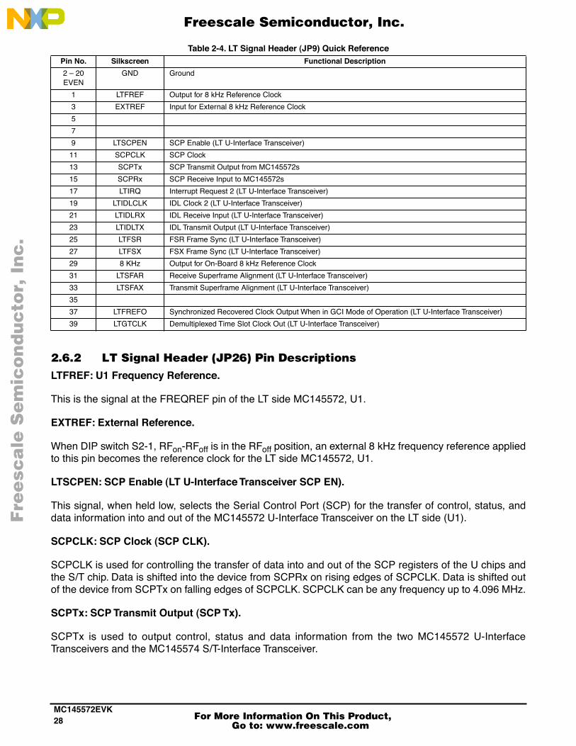
Table 2-4. LT Signal Header (JP9) Quick ReferencePin No. Silkscreen Functional Description
2 Ð 20 EVEN
GND Ground
1 LTFREF Output for 8 kHz Reference Clock
3 EXTREF Input for External 8 kHz Reference Clock
5
7
9 LTSCPEN SCP Enable (LT U-Interface Transceiver)
11 SCPCLK SCP Clock
13 SCPTx SCP Transmit Output from MC145572s
15 SCPRx SCP Receive Input to MC145572s
17 LTIRQ Interrupt Request 2 (LT U-Interface Transceiver)
19 LTIDLCLK IDL Clock 2 (LT U-Interface Transceiver)
21 LTIDLRX IDL Receive Input (LT U-Interface Transceiver)
23 LTIDLTX IDL Transmit Output (LT U-Interface Transceiver)
25 LTFSR FSR Frame Sync (LT U-Interface Transceiver)
27 LTFSX FSX Frame Sync (LT U-Interface Transceiver)
29 8 KHz Output for On-Board 8 kHz Reference Clock
31 LTSFAR Receive Superframe Alignment (LT U-Interface Transceiver)
33 LTSFAX Transmit Superframe Alignment (LT U-Interface Transceiver)
35
37 LTFREFO Synchronized Recovered Clock Output When in GCI Mode of Operation (LT U-Interface Transceiver)
39 LTGTCLK Demultiplexed Time Slot Clock Out (LT U-Interface Transceiver)
Fre
esc
ale
Se
mic
on
du
cto
r, I
Freescale Semiconductor, Inc.
For More Information On This Product, Go to: www.freescale.com
nc
...
29MC145572EVK
SCPRx: SCP Receive Input (SCP Rx).
SCPRX is used to input control, status, and data information to the two MC145572 U-Interface Transceiversand the MC145574 S/T-Interface Transceiver.
LTIRQ: Interrupt Request (LT U-Interface Transceiver IRQ).
The LTIRQ pin is an active low open drain output used to signal the MCU devices that an interrupt conditionexists in the LT MC145572 U-Interface Transceiver (U1). On clearing the interrupt condition, the LTIRQpin is returned to the high state.
LTIDLCLK: (LT U-Interface Transceiver Pin DCL).
This pin is an input when the MC145572 is in slave mode and an output when the MC145572 is in mastermode, as established by switch S2-2, MAS/SLV. As a timing master in LT mode, this pin provides a 512 kHz,2.048 MHz, or 2.56 MHz clock frequency. In GCI mode, the 2.56 MHz clock is not available. This choiceis programmed in BR7 or from the CLKSEL pin of the LT side MC145572. In GCI mode S5-4,GCI2048/GCI512 selects the clock rate on this pin. In slave mode, this pin accepts any clock frequencyfrom 512 kHz to 8.192 MHz, inclusive.
LTIDLRX: (LT U-Interface Transceiver Pin Din).
This pin is the input for the 2B+D data to be transmitted onto the LT U-Interface. Data bits are input onsequential falling edges of the LTIDLCLK signal, beginning immediately after the LTFSX pulse occurs. TheLTIDLRX pin is a donÕt care except during valid B- and D-channel data positions.
LTIDLTX: (LT U-Interface Transceiver Pin Dout).
This pin is the output for the 2B+D data received at the LT U-Interface. Data bits are output on rising edgesof the IDL CLK signal beginning immediately after the LTFSR pulse occurs. The LTIDLTX signal remainsin a high impedance state when not outputting 2B+D data or when a valid FS2 signal is missing.
LTFSR: (LT U-Interface Transceiver Pin FSR).
This pin is an input when the MC145572 is conÞgured for slave mode and an output when conÞgured formaster mode, as established by switch S2-2, MAS/SLV. In the master mode, this output is phase lockedto the 20.480 MHz clock of the LT side U chip. This signal is associated with data output from the Dout pinof the MC145572.
LTFSX: (LT U-Interface Transceiver Pin FSX).
This pin is an input when the MC145572 is conÞgured for slave mode and an output when conÞgured formaster mode, as established by switch S2-2, MAS/SLV. In the master mode, this output is phase lockedto the signal received at the LT U-Interface. This signal is associated with data input to the Din pin of theMC145572.
8 kHz: MC145572EVK Reference Clock.
This pin outputs an 8 kHz square wave that is generated by the on-board clock reference. This signal isavailable at all times.
LTSFAX: Transmit Superframe Alignment.
This pin carries a signal that indicates the Þrst 2B+D frame in a U superframe to be transmitted onto theU-Interface. This signal is not active when the LT side MC145572 is conÞgured for full GCI mode operation.
Fre
esc
ale
Se
mic
on
du
cto
r, I
Freescale Semiconductor, Inc.
For More Information On This Product, Go to: www.freescale.com
nc
...
MC145572EVK30
LTSFAR: Receive Superframe Alignment.
This pin carries a signal that indicates the Þrst 2B+D frame in a U superframe to be received from theU-Interface. This signal is not active when the LT side MC145572 is conÞgured for full GCI mode operation.
When the LT side MC145572 is conÞgured for full GCI mode operation, S2-5 in GCI position, this pinprovides the recovered timing clock. The frequency of the clock is selected between 2.048 MHz and512 kHz by the setting of S2-4, GCI2048/GCI512.
LTGTCLK: Gated IDL Clock Output.
This pin provides a gated clock output. The clock input of an external bit error rate tester should beconnected to this signal.
GND: Ground.
Negative Power Supply.
Table 2-5. NT and LT Side MC145572EVK Header List Header
Reference Function
J1 Access to LT Test Signals
J2 Access to LT 2B1Q Signal
J3 Short Positive Side of the Line to Ground
J4 Short Negative Side of the Line to Ground
J5 Tx/Rx Headers
J6 Access to LT TDM Signals
J7 LT RxDATA
J8 LT TxDATA
J9 Access to Multifunction MC145572 Pins
J10 LT CLK
J11 Access to Multifunction Pins
J12 Access to NT 2B1Q Signal
J13 Short Positive Side of the Line to Ground
J14 Short Negative Side of the Line to Ground
J15 Tx/Rx Header Pins
J17 Access to NT TDM Signals
J18 NT RxDATA
J19 Power Connector
J20 NT TxDATA
J21 NT CLK
J22 NT Data Interface Signals
J23 Access to SIT 2B1Q TE
J24 Access to SIT 2B1Q NT
JP1 LT PWR CONFIG
JP2 Short Line
JP3 Short R1
JP4 Short LT Sealing Current Blocking Cap
JP5 Short R6
JP6 Terminate Line with 135 W
JP7 Short Line
JP8 Short R17
JP9 Short N7 Sealing Current Blocking Cap
JP10 NT PWR CONFIG
Fre
esc
ale
Se
mic
on
du
cto
r, I
Freescale Semiconductor, Inc.
For More Information On This Product, Go to: www.freescale.com
nc
...
31MC145572EVK
2.7 DIP SWITCH FUNCTIONSFour sets of DIP switches are provided for MC145572EVK conÞguration and testing. These switches arepreset at the factory. In normal operation, the MC145572EVK is conÞgured for IDL operation with theMC68HC705 microcontroller communicating with the MC145572 U-Transceivers via the SCP interface.
NOTE
When a DIP switch is in the open position, the signal is at a logic 1. When a DIP switch isin the closed position, the signal is at a logic 0.
2.7.1 NT Side GCI Parameters DIP Switch S1This DIP switch is used to conÞgure the time slot and input pins of the NT side MC145572 when it isconÞgured for GCI mode by setting S4-4 to the GCI position. In normal operation, S4-4 is in the IDL positionand the settings of this DIP switch do not affect operation of the MC145572EVK.
JP11 Short R21
JP12 Terminate Line with 135 W
JP13 Swaps Tx and Rx Pins at J16
JP14 Default Termination Impedance on S/T Transmit
JP15 Default Termination Impedance on S/T Receive
Table 2-6. NT Side GCI Parameters DIP Switch S3
DIP Switch
Function
DescriptionFactory SettingOpen Closed
S3-1 S0HI S0LOW Program NT side MC145572 GCI S0 time slot select pin. S0HI
S3-2 S1HI S1LOW Program NT side MC145572 GCI S1 time slot select pin. S1H1
S3-3 S2HI S2LOW Program NT side MC145572 GCI S2 time slot select pin. S2HI
S3-4 GCI2048 GCI512 Select between 2.048 MHz and 512 kHz DCL clock when NT side MC145572 is in GCI mode.
GCI2048
S3-5 IN1HI IN1LOW Used to select level on IN1 pin of MC145572 when NT side MC145572 is in GCI mode.
IN2HI
S3-6 IN2HI IN2LOW Used to select level on IN2 pin of MC145572 when NT side MC145572 is in GCI mode.
IN2HI
Table 2-5. NT and LT Side MC145572EVK Header List (Continued)
Fre
esc
ale
Se
mic
on
du
cto
r, I
Freescale Semiconductor, Inc.
For More Information On This Product, Go to: www.freescale.com
nc
...
MC145572EVK32
2.7.2 NT Side Configuration DIP Switch S4This DIP switch is used to conÞgure operation of the NT side of the MC145572EVK. In particular, theMC145572 U-Interface Transceiver is conÞgurable for IDL or GCI operation, master or slave timing mode,and Parallel or Serial Control Port operation.
2.7.3 LT Side GCI Parameters DIP Switch S1This DIP switch is used to conÞgure the time slot and input pins of the LT side MC145572 when it isconÞgured for GCI mode by setting S2-5 to the GCI position. In normal operation, S2-5 is in the IDL2position and the settings of this DIP switch do not affect operation of the MC145572EVK.
Table 2-7. NT Side ConÞguration DIP Switch S4
DIP Switch
Function
DescriptionFactory SettingOpen Closed
S4-1 MAS SLV Selects the level on the M/S Pin to the NT1 U-Interface Transceiver. MAS
S4-2 FSR FSR=FSX Connects the FSR and FSX pins of the NT side MC145572 when closed. Use only in slave mode.
FSR
S4-3 8 10 Selects 10- or 8-bit mode gated IDL clock outputs for use with a bit error analyzer on the NT1 side when the MC145572 is conÞgured for MCU mode operation.
10
S4-4 IDL2 GCI When open, the MC145572 is conÞgured for MCU operation and the time division multiplexed bus interface to the MC145572 is in the IDL2 mode. When closed, the MC145572 is conÞgured for GCI operation and all 2B+D and control/status information is transferred over the GCI interface.
IDL2
S4-5 PAR SER Selects between the serial control port or parallel control port mode of accessing the NT side MC145572 when S4-4 is in the IDL2 mode position.
SER
S4-6 T_MAS T_SLV Selects between setting the MC145574 as a slave or master for the IDL2 bus. CLKHI
S4-7 RESMCU Controls the state of the microcontroller reset line. This is an input to the hardware reset of the MC68HC705C8 and is useful when using another platform to control the MC145572EVK. When closed, a reset signal is applied to U15.
OPEN
S4-8 FIX ADP Selects either the adaptive or the Þxed timing recovery mode for the S/T-Interface Transceiver.
ADP
S4-9 TE NT Selects the operating mode of the S/T-Interface Transceiver Ñ TE mode or NT mode. This signal is tied to the select lines of an analog multiplexer that conÞgures TE/NT(L) (U17-4),SG/DGRANT/ANDOUT (U17-8), and DREQUEST/ANDIN (U17-9) on the MC145574 appropriately.
TE
S4-10 NT1EN NT1DIS Turns NT1 function on or off. When the NT1 function is off, the user has complete control of all maintenance channel registers via the terminal interface. When open, the NT1 is enabled. When closed, the NT1 is disabled.
NTIDIS
Table 2-8. LT Side GCI Parameters DIP Switch S2
DIP Switch
Function
DescriptionFactory SettingOpen Closed
S1-1 S0HI S0LOW Program LT side MC145572 GCI S0 time slot select pin. S0HI
S1-2 S1HI S1LOW Program LT side MC145572 GCI S0 time slot select pin. S1HI
S1-3 S2HI S2LOW Program LT side MC145572 GCI S0 time slot select pin. S2HI
S1-4 GCI2048 GCI512 Select between 2.048 MHz and 512 kHz DCL clock when LT side MC145572 is in GCI mode.
GCI2048
S1-5 IN1HI IN1LOW Used to select level on IN1 Pin of MC145572 when LT side MC145572 is in GCI mode.
IN1HI
S1-6 IN2HI IN2LOW Used to select level on IN2 Pin of MC145572 when LT side MC145572 is in GCI mode.
IN2HI
Fre
esc
ale
Se
mic
on
du
cto
r, I
Freescale Semiconductor, Inc.
For More Information On This Product, Go to: www.freescale.com
nc
...
33MC145572EVK
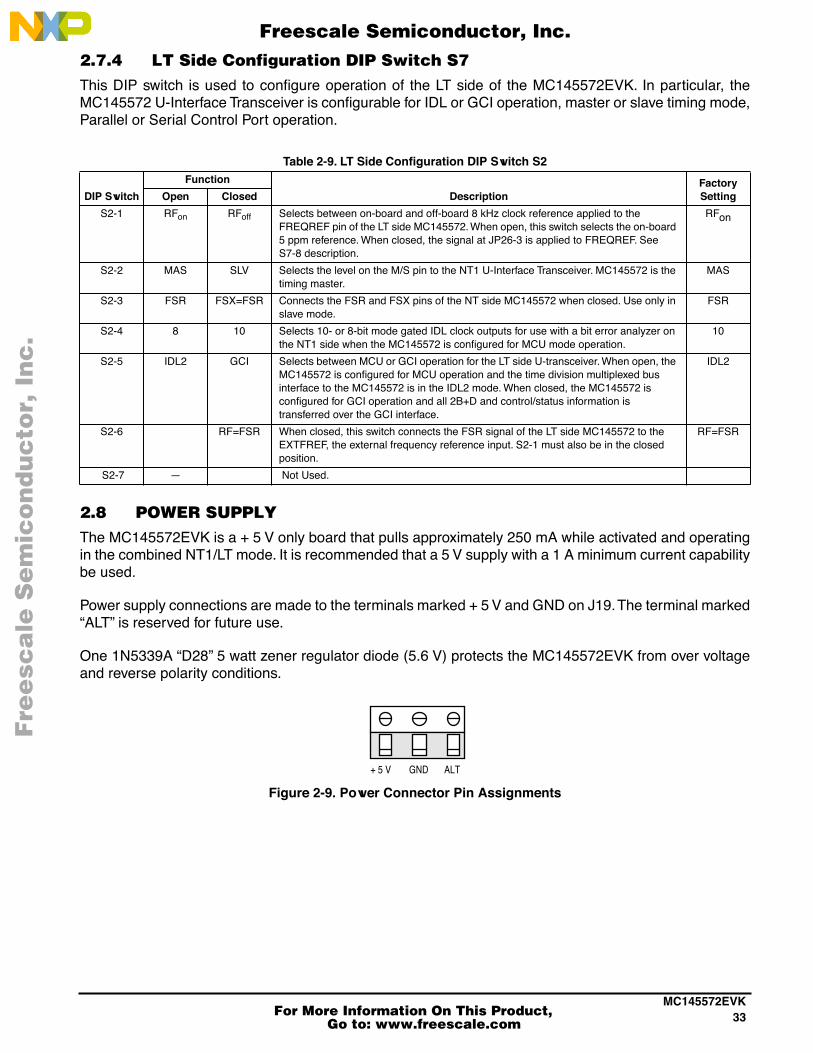
2.7.4 LT Side Configuration DIP Switch S7This DIP switch is used to conÞgure operation of the LT side of the MC145572EVK. In particular, theMC145572 U-Interface Transceiver is conÞgurable for IDL or GCI operation, master or slave timing mode,Parallel or Serial Control Port operation.
2.8 POWER SUPPLYThe MC145572EVK is a + 5 V only board that pulls approximately 250 mA while activated and operatingin the combined NT1/LT mode. It is recommended that a 5 V supply with a 1 A minimum current capabilitybe used.
Power supply connections are made to the terminals marked + 5 V and GND on J19. The terminal markedÒALTÓ is reserved for future use.
One 1N5339A ÒD28Ó 5 watt zener regulator diode (5.6 V) protects the MC145572EVK from over voltageand reverse polarity conditions.
Figure 2-9. Power Connector Pin Assignments
Table 2-9. LT Side ConÞguration DIP Switch S2
DIP Switch
Function
DescriptionFactory SettingOpen Closed
S2-1 RFon RFoff Selects between on-board and off-board 8 kHz clock reference applied to the FREQREF pin of the LT side MC145572. When open, this switch selects the on-board 5 ppm reference. When closed, the signal at JP26-3 is applied to FREQREF. See S7-8 description.
RFon
S2-2 MAS SLV Selects the level on the M/S pin to the NT1 U-Interface Transceiver. MC145572 is the timing master.
MAS
S2-3 FSR FSX=FSR Connects the FSR and FSX pins of the NT side MC145572 when closed. Use only in slave mode.
FSR
S2-4 8 10 Selects 10- or 8-bit mode gated IDL clock outputs for use with a bit error analyzer on the NT1 side when the MC145572 is conÞgured for MCU mode operation.
10
S2-5 IDL2 GCI Selects between MCU or GCI operation for the LT side U-transceiver. When open, the MC145572 is conÞgured for MCU operation and the time division multiplexed bus interface to the MC145572 is in the IDL2 mode. When closed, the MC145572 is conÞgured for GCI operation and all 2B+D and control/status information is transferred over the GCI interface.
IDL2
S2-6 RF=FSR When closed, this switch connects the FSR signal of the LT side MC145572 to the EXTFREF, the external frequency reference input. S2-1 must also be in the closed position.
RF=FSR
S2-7 Ñ Not Used.
+ 5 V GND ALT
Fre
esc
ale
Se
mic
on
du
cto
r, I
Freescale Semiconductor, Inc.
For More Information On This Product, Go to: www.freescale.com
nc
...
MC145572EVK34
3
SOFTWARE DESIGN DESCRIPTION
3.1 OPERATING PROCEDURESA resident terminal program permits the user to interact with the MC145572EVK. The commands providethe following functions:
a. Activation with or without loop-backs.
b. ModiÞcations to and displays of registers.
c. ModiÞcations to and status of eoc functions.
d. Deactivation options.
3.1.1 Power On Reset and Terminal PromptApplying power to the MC145572EVK causes a power on reset to occur which invokes the resident terminalprogram.
1. When the terminal is connected to the NT1 side EIA-232 connector (J16), the terminal displaysthe following:
MC145572EVK EVALUATION CARD Vx.x
MC68HC705C8 VERSION
NTLT>
where: x.x is the software revision number.
3.1.2 Command Line InterfaceAfter initialization or return of control to the monitor, the terminal displays the ÒNTLT>Ó prompt. If an invalidcommand is entered, Ò! INVALID COMMAND !Ó is displayed on the terminal. This error message isaccompanied by a BELL. All erroneous commands are accompanied by an appropriate error messageaccompanied by a BELL.
The MC145572EVK waits for a command line input from the terminal. All commands can be entered aslower or upper case. When a valid command has been entered, the command is executed or a menu isbrought up. All menus prompt the user for appropriate inputs to select a function or to quit the menu.
Fre
esc
ale
Se
mic
on
du
cto
r, I
Freescale Semiconductor, Inc.
For More Information On This Product, Go to: www.freescale.com
nc
...
35MC145572EVK
NOTE
The terminal interface does NOT have multiple character type ahead.
3.1.3 Push-Button ActivationOne push-button is provided for activating/deactivating the U-Interface Transceivers without the necessityof using a terminal. The activate push-button (PB2) can be pressed to activate/deactivate the U-interface.Pressing the activate push-button toggles the current activation mode. If the U-Interface Transceiver(s) isnot activated, pressing the activate push-button activates it. If the U-Interface Transceiver(s) is activated,pressing the activate push-button deactivates it.
Immediately following a reset, the board can be activated as an NT1 by pressing the activate push-button,and the LT side U-Interface Transceiver will also attempt to activate. If there is no connection to the LT sideU-interface, the LT U-Interface Transceiver will not activate and an error condition will be displayed on theLT side status LEDs. The same is true if there is no connection to the NT1 side U-Interface Transceiver,except that the error status is displayed on the NT1 side LEDs.
3.1.4 General Comments About ActivationThe monitor software continually tests for a U-Interface Transceiver activation in progress. If this is detected,the monitor automatically executes the appropriate activation routine(s).
Activation status is monitored visually from the status LEDs on each half of the board. When activation isin progress, the TP/AIP LED turns on. All other LEDs are off. Successful activation is indicated by all LEDsexcept for the EI LED being turned on. When activation fails, only the EI LED turns on.
3.1.5 Embedded Operations Channel, Register R6The embedded operations channel register is a 12-bit register that appears in the U-Interface Transceivernibble register memory map, referred to as R6 in the MC145572 data sheet. It is written to or read fromby using either the NRL or NRN commands with register 6 speciÞed. The monitor always echoes back theregister name as R6, not NR6.
EXAMPLE
NTLT>NRN 6 152 Write hex 152 to eoc framer
R6:152 Updated R6 echoed to terminal
NTLT> Command line prompt
3.2 COMMAND SETThe following pages deÞne the command set to be used with the aid of an external terminal.
A summary of the MC145572EVK software command set:
ACT: Activation/Deactivation Menu
BRL: Read/Write LT U-Interface Transceiver Byte Register
BRN: Read/Write NT U-Interface Transceiver Byte Register
BRS: Read/Write S/T-Interface Transceiver Byte Register
Fre
esc
ale
Se
mic
on
du
cto
r, I
Freescale Semiconductor, Inc.
For More Information On This Product, Go to: www.freescale.com
nc
...
MC145572EVK36
BRT: Read/Write S/T-Interface Transceiver Byte Register, Alternate Form
CLR: Clears febe/nebe, Re-Enters BR4 and BR5 in Both LT and NT Side U-Transceivers
DEA: Activation/Deactivation Menu, Alternate Form
DIS: Display Formatted Registers
EOC: Embedded Operations Channel Menu
HEL: Help Menu
LOF: Disable LT M4 Handler
LON: Enable LT M4 Handler
LPU: U-Interface Transceiver Analog Loop-Back
MM: Modify Memory
NOF: Disable NT1
NON: Enable NT1
NRL: Read/Write LT U-Interface Transceiver Nibble Register
NRN: Read/Write NT U-Interface Transceiver Nibble Register
NRS: Read/Write S/T-Interface Transceiver Nibble Register
NRT: Read/Write S/T-Interface Transceiver Nibble Register, Alternate Form
ORL: Read/Write LT U-Interface Transceiver Overlay Register
ORN: Read/Write NT U-Interface Transceiver Overlay Register
RES: Reset S/T and/or U-Interface Transceivers
3.2.1 ACT — Activation/Deactivation Menu
3.2.1.1 FORMAT.
ACT<ENTER>
The activation/deactivation menu permits selection of various activation modes that can be invoked. Allor speciÞc U-Interface Transceivers or S/T-Interface Transceivers can be activated or deactivated in acontrolled manner. After any of the activation options have been invoked, the MC145572EVK executes aÒDISÓ command and dumps all of the U- and S/T-Interface Transceiver registers to the screen before issuinga prompt to the terminal.
One or both U-Interface Transceiver(s) can be activated by selecting the appropriate menu option. Optionsare available to permit activation along with putting the MC145572EVK board into various loop-back modesfor performance testing purposes. When the U- and S/T-Interface Transceivers are activated, transparentdata transfer is always enabled so user equipment can be connected to the IDL Interface on the NT1 andLT sides of the MC145572EVK.
Fre
esc
ale
Se
mic
on
du
cto
r, I
Freescale Semiconductor, Inc.
For More Information On This Product, Go to: www.freescale.com
nc
...
37MC145572EVK
3.2.1.2 LOOP-BACK OPTIONS. The activate command provides Þve different points on theMC145572EVK board where loop-backs are permitted when one or both U-Interface Transceivers areactivated. At any given time, only one loop-back point can be enabled. This permits user equipment to beconnected to the opposite side of the MC145572EVK. For example, if a loop-back is selected on the NT1half of the board, user equipment can be connected to the IDL Interface on the LT side of theMC145572EVK.
The LT side U-Interface Transceiver can be activated with 2B+D loop-back to the U-Interface. This modeenables the received digital data from the U-Interface to be looped back to the LT side U-InterfaceTransceiver transmitter, and re-transmitted onto the U-Interface. The loop-back point occurs in the IDLInterface block internal to the U-Interface Transceiver.
The LT side U-Interface Transceiver can also be activated without any loop-backs initially enabled. Aloop-back is then implemented simply by shorting BNC J7 RXDATA to BNC J8 LTXDATA.
The NT1 side U-Interface Transceiver can be activated with 2B+D loop-back enabled in the S/T-InterfaceTransceiver IDL Interface. Received data from the NT1 side U-Interface Transceiver is transmitted on theIDL Interface to the S/T-Interface Transceiver where it is looped-back to the IDL Interface and re-transmittedby the NT1 U-Interface Transceiver towards the U-Interface.
The NT1 side U-Interface Transceiver can be activated with the S/T-Interface Transceiver disabled. Thiscauses the S/T-Interface Transceiver to three-state its IDL Interface transmitter. This provides the NT1 sideU-Interface Transceivers IDL Interface direct access to the NT1 side IDL Interface. This permits the userto connect their own equipment to the NT1 side IDL Interface without any possibility of bus contention withthe S/T-Interface Transceiver.
The NT1 side U-Interface Transceiver can also be activated without any loop-back. This permits the NT1side U-Interface Transceiver to communicate with the S/T-Interface Transceiver over the IDL Interface. Aloop-back is implemented by shorting BNC J18 NTRXDATA to BNC J20 NTTXDATA.
3.2.1.3 MENUS.
Operation With the MC145572EVK Board
The ACT command provides user access to the full set of activation and deactivation options. Four menuoption groups are displayed on the terminal.
Options A through D permit activation of the NT1 side U-Interface Transceiver independently of the LTside U-Interface Transceiver. These options would typically be used when the NT1 side U-Interface isconnected to an incoming 2B1Q line from a central ofÞce, or to the LT side U-Interface connector on asecond MC145572EVK.
Options E and F permit activation of the LT side U-Interface Transceiver independently of the NT1 sideU-Interface Transceiver. These options would typically be used when the LT side U-Interface is connectedto a separate NT1 or to the NT1 side U-Interface connector on a second MC145572EVK.
Options G through J are used when the LT side and the NT1 side U-Interface connectors on anMC145572EVK are connected together.
Options K through O are used to deactivate the U- and S/T-Interface Transceivers in a controlled manner.
EXAMPLE 1
NTLT>act
Fre
esc
ale
Se
mic
on
du
cto
r, I
Freescale Semiconductor, Inc.
For More Information On This Product, Go to: www.freescale.com
nc
...
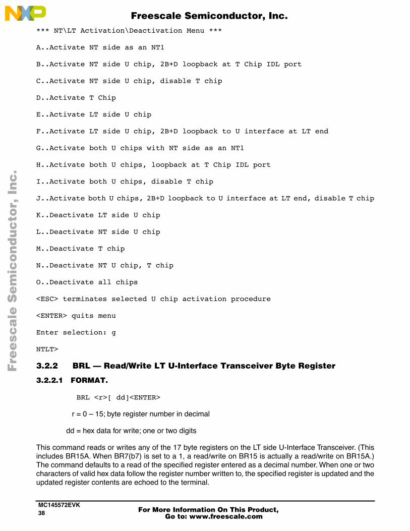
MC145572EVK38
*** NT\LT Activation\Deactivation Menu ***
A..Activate NT side as an NT1
B..Activate NT side U chip, 2B+D loopback at T Chip IDL port
C..Activate NT side U chip, disable T chip
D..Activate T Chip
E..Activate LT side U chip
F..Activate LT side U chip, 2B+D loopback to U interface at LT end
G..Activate both U chips with NT side as an NT1
H..Activate both U chips, loopback at T Chip IDL port
I..Activate both U chips, disable T chip
J..Activate both U chips, 2B+D loopback to U interface at LT end, disable T chip
K..Deactivate LT side U chip
L..Deactivate NT side U chip
M..Deactivate T chip
N..Deactivate NT U chip, T chip
O..Deactivate all chips
<ESC> terminates selected U chip activation procedure
<ENTER> quits menu
Enter selection: g
NTLT>
3.2.2 BRL — Read/Write LT U-Interface Transceiver Byte Register
3.2.2.1 FORMAT.
BRL <r>[ dd]<ENTER>
r = 0 Ð 15; byte register number in decimal
dd = hex data for write; one or two digits
This command reads or writes any of the 17 byte registers on the LT side U-Interface Transceiver. (Thisincludes BR15A. When BR7(b7) is set to a 1, a read/write on BR15 is actually a read/write on BR15A.)The command defaults to a read of the speciÞed register entered as a decimal number. When one or twocharacters of valid hex data follow the register number written to, the speciÞed register is updated and theupdated register contents are echoed to the terminal.
Fre
esc
ale
Se
mic
on
du
cto
r, I
Freescale Semiconductor, Inc.
For More Information On This Product, Go to: www.freescale.com
nc
...
39MC145572EVK
NOTE
If the RO/WO bit in U-Interface Transceiver BR14 is not set, the data echoed back may notbe the same as the data written to the byte register.
EXAMPLE
NTLT>BRL 6 1 Enable IDL 2B+D loop-back transparent
BR6:01 Updated BR6 echoed to terminal
NTLT> Command line prompt
3.2.3 BRN — Read/Write NT U-Interface Transceiver Byte Register
3.2.3.1 FORMAT.
BRN <r>[ dd]<ENTER>
r = 0 Ð 15; byte register number in decimal
dd = hex data for write; one or two digits
This command reads or writes any of the 17 byte registers on the LT side U-Interface Transceiver. (Thisincludes BR15A. When BR7(b7) is set to a 1, a read/write on BR15 is actually a read/write on BR15A.)The command defaults to a read of the speciÞed register entered as a decimal number. When one or twocharacters of valid hex data follow the register number written to, the speciÞed register is updated and theupdated register contents are echoed to the terminal.
NOTE
If the RO/WO bit in U-Interface Transceiver BR14 is not set, the data echoed back may notbe the same as the data written to the byte register.
EXAMPLE
NTLT>BRN 6 1 Enable IDL 2B+D loop-back transparent
BR6:01 Updated BR6 echoed to terminal
NTLT> Command line prompt
3.2.4 BRS — Read/Write S/T-Interface Transceiver Register
3.2.4.1 FORMAT.
BRS <r>[ dd]<ENTER>
r = 0 Ð 15; byte register number in decimal
dd = hex data for write; one or two digits
The BRS command reads or writes any of the 16 byte registers on the S/T-Interface Transceiver. BRS andBRT are alternate forms of the same command. The command defaults to a read of the speciÞed register.The register number is entered as a decimal number. When one or two characters of valid hex data follow
Fre
esc
ale
Se
mic
on
du
cto
r, I
Freescale Semiconductor, Inc.
For More Information On This Product, Go to: www.freescale.com
nc
...
MC145572EVK40
the register number written to, the speciÞed register is updated and the updated register contents areechoed to the terminal.
NOTE
Bits that are read only/write only bits may not necessarily reßect the value written to themwhen echoed to the terminal.
EXAMPLE
NTLT>BRS 6 1 Enable IDL B2 loop-back non-transparent
BR6:01 Updated BR6 echoed to terminal
NTLT>BRS 14 aa Write hex aa to byte register 14
BR14:AA Updated BR14 echoed to terminal
NTLT> Command line prompt
3.2.5 BRT — Read/Write S/T-Interface Transceiver Byte Register
3.2.5.1 FORMAT.
BRT <r>[ dd]<ENTER>
r = 0 Ð 15; byte register number in decimal
dd = hex data for write; one or two digits
BRT is an alternate form of the BRS command. For a complete description, see BRS.
3.2.6 CLR — Clear febe/nebe Registers
3.2.6.1 FORMAT.
CLR<ENTER>
This command is used to clear the febe and nebe registers. BR4 and BR5, for both LT and NT sideU-Transceivers. This is very useful when doing bit error tests.
3.2.7 DEA — Activation/Deactivation Menu
3.2.7.1 FORMAT.
DEA<ENTER>
DEA is an alternate form of ACT. For a complete description, see ACT.
3.2.8 DIS — Display Formatted Registers
3.2.8.1 FORMAT.
DIS[device]<ENTER>
Where device:
Fre
esc
ale
Se
mic
on
du
cto
r, I
Freescale Semiconductor, Inc.
For More Information On This Product, Go to: www.freescale.com
nc
...
41MC145572EVK
= N (NT side U-Interface Transceiver register set)
= L (LT side U-Interface Transceiver register set)
= S (S/T-Interface Transceiver register set)
= T (S/T-Interface Transceiver register set)
= A (all chips)
= U (both U-Interface Transceivers on-board)
NOTE
If DIS<ENTER> is given, the command defaults to display all registers.
This command displays the entire register set of the selected chip(s) on the terminal. The display isformatted by speciÞc IC. When a U-Interface Transceiver register set is displayed, the Þrst line for that chipshows the six nibble registers followed by the eoc register, R6. When an S/T-Interface Transceiver registerset is displayed, the Þrst line for that chip shows the seven nibble registers. For both the U-InterfaceTransceiver and the S/T-Interface Transceiver, byte registers 0 Ð 7 are displayed on the second output linefor the chip, and byte registers 8 Ð 15 are displayed on the third output line for the chip. The U-InterfaceTransceiver register R6 is in the nibble register memory map and has three characters in its data Þeld.Byte register 15A is displayed on the fourth line for the U-Interface Transceivers.
EXAMPLE
Display all register sets.
NTLT>dis
MC145472 U-Chip Register Contents (LT)
NR0:0 NR1:B NR2:1 NR3:4 NR4:0 NR5:0 R6:1AA
BR0:FF BR1:FF BR2:FF BR3:FD BR4:FF BR5:00 BR6:00 BR7:00
BR8:30 BR9:90 BR10:90 BR11:A7 BR12:06 BR13:83 BR14:01 BR15:08
BR15A:08
OR0:00 OR1:04 OR2:8 OR3:00 OR4:04 OR5:08 OR6:E0 OR7:00
OR8:00 OR9:00
MC145472 U-Chip Register Contents (NT)
NR0:0 NR1:B NR2:1 NR3:4 NR4:0 NR5:0 R6:114
BR0:FF BR1:FF BR2:FF BR3:FD BR4:FF BR5:FF BR6:00 BR7:00
BR8:31 BR9:10 BR10:10 BR11:A7 BR12:06 BR13:34 BR14:01 BR15:08
BR15A:08
Fre
esc
ale
Se
mic
on
du
cto
r, I
Freescale Semiconductor, Inc.
For More Information On This Product, Go to: www.freescale.com
nc
...
MC145572EVK42
OR0:00 OR1:04 OR2:8 OR3:00 OR4:04 OR5:08 OR6:E0 OR7:00
OR8:00 OR9:00
MC145574 S-T Chip Register Contents
NR0:0 NR1:B NR2:1 NR3:8 NR4:0 NR5:0 NR6:8
BR0:00 BR1:00 BR2:00 BR3:F0 BR4:00 BR5:00 BR6:00 BR7:00
BR8:C0 BR9:00 BR10:00 BR11:00 BR12:00 BR13:00 BR14:00 BR15:4C
NTLT>
3.2.9 eoc — Embedded Operations Channel Menu
3.2.9.1 FORMAT.
eoc<ENTER>
This command brings up the status of the embedded operations channels on the LT and NT1 sideU-Interface Transceivers. If the board is being operated from the NT1 half, a menu is displayed whichpermits the user to select an eoc message to be sent from the NT1 to the LT when a loop is activated.The appropriate LT or NT U-Interface Transceiver eoc status displays are brought up depending on theboard conÞguration.
3.2.9.2 eoc MENU DESCRIPTION. The eoc menu divides an eoc command into two parts: theaddress nibble and the message byte, for a total of 12 bits. The address nibble holds the ANSI T1.601-1992deÞned 3-bit address and the message/data bit. The ANSI T1.601-1992 deÞned embedded operationschannel address is stored in bits 3, 2, and 1 of the address nibble. This corresponds to the ANSIT1.601-1992 deÞned bits, eoc(a1), eoc(a2), and eoc(a3), respectively. Bit 0 of the address nibblecorresponds to ANSI T1.601-1992 deÞned bit eoc(dm). Menu items I and J permit manipulation of theANSI T1.601-1992 eoc address and message/data bit which are stored as the default address nibble.Menu items A through H permit the user to select a predeÞned message byte or permit the user to createa custom message byte. The MC145572EVK software creates an eoc command by concatenating thedefault address nibble and the message byte to create a 12-bit eoc command. The 12-bit eoc commandis loaded into R6 and sent on the next eoc frame boundary. The MC145572EVK software treats the addressnibble and the message byte as independent entities.
NOTE
The RES command does not affect the setting of the current eoc default address nibble.At power up, it is binary 0001. It can only be changed by selecting eoc menu options I or J.
The menu permits the user to send standard eoc message codes, set a new default eoc address nibble,or send a custom 8-bit eoc message appended to the current default eoc address nibble. After each menuoption has been executed, the menu is displayed again. The menu can be exited by pressing the <ENTER>key. In normal operation, menu items A through G are used. Menu items H, I, and J are used if a differentdefault address is desired, or when eoc commands are being transmitted to an NT1 that uses non-ANSIstandard eoc commands. The eoc menu appears when the MC145572EVK is conÞgured as NT/LT.
The most signiÞcant nibble is the eoc address nibble. These four bits are set to a default value of 0001binary when the MC145572EVK is reset. The three most signiÞcant bits (000) indicate NT1 address, andthe least signiÞcant bit, which is a 1, indicates that an eoc message is being sent. The ANSI standard
Fre
esc
ale
Se
mic
on
du
cto
r, I
Freescale Semiconductor, Inc.
For More Information On This Product, Go to: www.freescale.com
nc
...
43MC145572EVK
indicates that when the least signiÞcant bit of the address nibble is a 0, then eoc data is being transmitted.In ANSI terminology, the address nibble is referred to as the address/message indicator.
The software on the MC145572EVK only responds to eoc addresses of 000 or 111, the broadcast address.The message bit must be a 1 and only the seven ANSI deÞned eoc commands are supported. These are,in hexadecimal:
50 Loop-back 2B+D channels at NT1
51 Loop-back B1 channel at NT1
52 Loop-back B2 channel at NT1
53 Request corrupted crc to be sent from NT1 to LT
54 Notify NT1 of incoming corrupt crc from LT
FF Return NT1 to normal operation
00 Hold NT1 in current state
For example: with the default eoc address nibble equal to 1, the MC145572EVK would load 150 into theLT U-Interface Transceiver nibble register 6 when menu item C is selected. This would be loaded into theLT U-Interface Transceiver eoc framer register, R6, and transmitted to the NT1.
The menu permits a new default value to be selected for the eoc address nibble. This is menu item J. Thesoftware also permits a custom eoc message to be concatenated with the current default eoc addressnibble. This is done by selecting menu item H. After the custom eoc message has been entered, it isconcatenated with the current default eoc address nibble and the 12 bits are loaded into the LT U-InterfaceTransceiver eoc framer register, R6, and transmitted to the NT1.
EXAMPLE 1
MC145572EVK:
NTLT>eoc
eoc commands sent from LT
B1 Loopback....OFF Request corrupt crc.....OFF
B2 Loopback....ON Notify corrupt crc......OFF
D Loopback....OFF NT1 hold state..........OFF
Last eoc sent: FFF Last eoc received: 151
eoc commands received at NT
B1 Loopback....OFF Request corrupt crc.....OFF
B2 Loopback....ON Notify corrupt crc......OFF
D Loopback....OFF NT1 hold state..........OFF
Fre
esc
ale
Se
mic
on
du
cto
r, I
Freescale Semiconductor, Inc.
For More Information On This Product, Go to: www.freescale.com
nc
...
MC145572EVK44
Last eoc sent: FFF Last eoc received: 151
**** LT End eoc Menu ****
A..B1 loopback at NT1 F..Return NT1 to normal
B..B2 loopback at NT1 G..Hold NT1
C..2B+D loopback at NT1 H..Send custom eoc message
D..NT1 send bad crc I..Set default eoc address
E..Notify NT1 of bad crc J..eoc address = NT1 (0001)
<ENTER> quits menu
Enter desired selection: <ENTER>
NTLT>
3.2.10 HEL — Help Menu
3.2.10.1 FORMAT.
HEL<ENTER>
or
?
This command dumps a summary of the command set to the terminal.
EXAMPLE
NTLT>hel
ACT or DEA Activate\deactivate menu
EOC eoc menu
DIS[ A][ L][ N][ S][ T][ U] Display registers
RES[ A][ L][ N][ S][ T][ U] Reset
BR<L><N><S><T> r[ dd] R\W byte register r
OR<L><N> r[ dd] R\W MC145572 overlay register r
r = 0 Ð 15, dd = 0 Ð FF
NR<L><N><S><T> r[ d] [ ddd] R\W nibble register r
r = 0 Ð 6, d = 0 Ð F, ddd for U chip R6
LPU <N><L> U chip analog loop-back
Fre
esc
ale
Se
mic
on
du
cto
r, I
Freescale Semiconductor, Inc.
For More Information On This Product, Go to: www.freescale.com
nc
...
45MC145572EVK
MM AA[ dd] R/W memory adr AA
AA = 0 Ð FF, dd = 0 Ð FF
CLR Clear all febe/nebe registers
LON LT M4 handler on
LOF LT M4 handler off
NON NT1 enabled
NOF NT1 disabled
U: U chips, L: LT U chip, N: NT U chip, S or T: T chip, A: all
< >:required option
NTLT>
3.2.11 LOF — Disable LT M4 Handler
3.2.11.1 FORMAT.
LOF<ENTER>
This command turns off automatic control of the M4 ACT bit at the LT. The M4 messages must be handledmanually via the byte register commands.
3.2.12 LON — Enable LT M4 Handler
3.2.12.1 FORMAT.
LON<ENTER>
This command enables automatic handling of the LT side M4 channel by the MC68HC705C8 MCU. Thisis the default operating mode of the EVK board after reset.
3.2.13 LPU — U-Interface Transceiver Analog Loop-Backs
3.2.13.1 FORMAT.
LPU <n> <ENTER>
device = N (selects NT side ÒU-ChipÓ)
= L (selects LT side ÒU-ChipÓ)
NOTE
The U-Interface connector should have a 135 W terminator connected.
This command puts a U-Interface Transceiver into special loop-back and test modes for individual testing.When an LPU command is invoked, the register set of the corresponding U-Interface Transceiver is alwaysdisplayed before the command line prompt is written to the terminal. It is advisable to reset the
Fre
esc
ale
Se
mic
on
du
cto
r, I
Freescale Semiconductor, Inc.
For More Information On This Product, Go to: www.freescale.com
nc
...
MC145572EVK46
MC145572EVK after invoking any of the LPU commands. Each U-Interface Transceiver can beindependently put into analog loop-back.
The echo canceller loop-back is an external analog loop-back where data received on the U-InterfaceTransceiver IDL Rx pin is framed up and then transmitted as 2B1Q symbols. The 2B1Q symbols arereceived by the U-Interface Transceiver and cancelled by the echo canceller. Only the echo cancellers areenabled during this mode. When the U-Interface Transceiver is operating correctly, BR12+BR13 shouldhave a low value. Preferably, BR12 should be 00 and BR13 should be a low value. BR13 will continue toßuctuate in value slightly. BR11 should read as 10 or 11. Several seconds may elapse before the registersreach a steady state and the correct bits are set.
Fre
esc
ale
Se
mic
on
du
cto
r, I
Freescale Semiconductor, Inc.
For More Information On This Product, Go to: www.freescale.com
nc
...
47MC145572EVK
EXAMPLE
NTLT>lpu n
NTLT>dis n
MC145472 U Chip Register Contents (NT)
NR0 : 0 NR1 : B NR2 : 0 NR3 : 5 NR4 : 0 NR5 : 0
R6 : 1FF
BR0 : 77 BR1 : 7F BR2 : F0 BR3 : F9 BR4 : FF BR5 : C2
BR6 : 00 BR7 : 04
BR8 : 31 BR9 : 80 BR10 : 00 BR11: 47 BR12: 03 BR13: 64
BR14: 00 BR15: 46
BR15A(R) : 1E BR15A(W) : 00
OR0 : 00 OR1 : 00 OR2 : 00 OR3 : 00 OR4 : 00 OR5 : 00
OR6 : 00 OR7 : 20
OR8 : 08 OR9 : 00
NTLT>
3.2.14 MM — Modify Memory
3.2.14.1 FORMAT.
mm aa[ dd]<ENTER>
aa = hex address for read or write; one or two digits
dd = hex data for write; one or two digits
NOTE
This is a very dangerous command to use. Please do not use it if you do not have a sourcecode listing and a copy of the MC68HC705C8 data book.
This command reads or writes any of the 68HC705C8 memory addresses between hexadecimal 00 andhexadecimal FF. The command defaults to a read of the speciÞed memory address. When one or twocharacters of valid hex data follow the memory address written to, the speciÞed address is updated andits contents are echoed to the terminal. This command is very useful for reading and writing the I/O portof the MC68HC705 microcontroller.
This command accesses the memory addresses on the NT1 half of the board.
Fre
esc
ale
Se
mic
on
du
cto
r, I
Freescale Semiconductor, Inc.
For More Information On This Product, Go to: www.freescale.com
nc
...
MC145572EVK48
EXAMPLE
NTLT>mm 51 Read address 51
51:xx Unknown data read from address 51
NTLT>mm 51 2E Write hex 2E to address 51
51:2E Echo updated contents to terminal
NTLT> Command line prompt
3.2.15 NOF — Disable NT1 Function
3.2.15.1 FORMAT.
NOF<ENTER>
This command disables all NT1 functions on the board. This permits the user to have total manual controlover maintenance channels on the NT via the nibble and byte register commands.
3.2.16 NON — Enable NT1 Function
3.2.16.1 FORMAT.
NON<ENTER>
This command enables the functional NT1. This means that maintenance channel messages are alsoautomatically serviced by the MCU. This is the default condition of the EVK after a reset.
3.2.17 NRL — Read/Write LT U-Interface Transceiver Nibble Register
3.2.17.1 FORMAT.
NRL <r>[ d] <ENTER>
NRL 6[ddd] <ENTER>
r = 0 Ð 6
[ d][ ddd]= hex data for write
NOTE
All three digits required, no spaces, for write to nibble register 6.
The NRL command reads or writes any of the seven registers in the nibble register memory map on theLT side U-Interface Transceiver. The command defaults to a read of the speciÞed register. The registernumber is entered as a decimal number. When a valid hexadecimal character follows the register numberwritten to, the speciÞed register is updated and the contents are echoed to the terminal. The eoc register,R6, is accessed by entering ÒNRL 6 [ddd].Ó This reads/writes the eoc (R6) register which is a 12-bit registerappearing in the nibble register memory map.
Fre
esc
ale
Se
mic
on
du
cto
r, I
Freescale Semiconductor, Inc.
For More Information On This Product, Go to: www.freescale.com
nc
...
49MC145572EVK
NOTE
Bits that are read only/write only may not necessarily reßect the value written to them whenechoed to the terminal.
EXAMPLE
NTLT>NRL 4 1 Enable M5/M6 channel interrupts
NR4:1 Updated NR4 echoed to terminal
NTLT>BRL 14 40 Make all registers read/write
BR14:40 Updated BR14 echoed to terminal
NTLT>NRL 6 151 Write hex 151 to eoc framer
R6:151 Updated R6 echoed to terminal
NTLT> Command line prompt
3.2.18 NRN — Read/Write NT U-Interface Transceiver Nibble Register
3.2.18.1 FORMAT.
NRN <r>[ d] <ENTER>
NRN 6[ddd] <ENTER>
r = 0 Ð 6
[ d][ ddd]= hex data for write
NOTE
All three digits required, no spaces, for write to nibble register 6.
The NRN command reads or writes any of the seven registers in the nibble register memory map on theNT1 side U-Interface Transceiver. The command defaults to a read of the speciÞed register. The registernumber is entered as a decimal number. When a valid hexadecimal character follows the register numberwritten to, the speciÞed register is updated and the contents are echoed to the terminal. The eoc register,R6, is accessed by entering ÒNRN 6 [ddd].Ó This reads/writes the eoc (R6) register, which is a 12-bit registerappearing in the nibble register memory map.
NOTE
Bits that are read only/write only may not necessarily reßect the value written to them whenechoed to the terminal.
EXAMPLE
NTLT>NRN 5 2 Block channel B2
NR5:2 Updated NR5 echoed to terminal
NTLT>BRN 14 40 Make all registers read/write
Fre
esc
ale
Se
mic
on
du
cto
r, I
Freescale Semiconductor, Inc.
For More Information On This Product, Go to: www.freescale.com
nc
...
MC145572EVK50
BR14:40 Updated BR14 echoed to terminal
NTLT>NRN 6 152 Write hex 152 to eoc framer
R6:152 Updated R6 echoed to terminal
NTLT> Command line prompt
3.2.19 NRS — Read/Write S/T-Interface Transceiver Nibble Register
3.2.19.1 FORMAT.
NRS <r>[ d]<ENTER>
r = 0 Ð 6 for register number
d = hex data for write; one digit
The NRS command reads or writes any of the seven nibble registers on the S/T-Interface Transceiver.NRS and NRT are alternate forms of the same command. The command defaults to a read of the speciÞedregister. The register number is entered as a decimal number. When a valid hexadecimal character followsthe register number written to, the speciÞed register is updated and the contents are echoed to the terminal.
NOTE
Bits that are read only/write only may not necessarily reßect the value written to them whenechoed to the terminal.
EXAMPLE
NTLT>NRS 6 8 Enable 2B+D non-transparent loop-back
NR6:8 Updated NR6 echoed to terminal
NTLT> Command line prompt
3.2.20 NRT — Read/Write S/T-Interface Transceiver Nibble Register
3.2.20.1 FORMAT.
NRT <r>[ d]<ENTER>
r = 0 Ð 6 for register number
d = hex data for write; one digit
NRT is an alternate form of the NRS command. For a complete description, see NRS.
Fre
esc
ale
Se
mic
on
du
cto
r, I
Freescale Semiconductor, Inc.
For More Information On This Product, Go to: www.freescale.com
nc
...
51MC145572EVK
3.2.21 ORL — Read/Write LT U-Interface Transceiver Byte Register
3.2.21.1 FORMAT.
ORL <r>[ dd]<ENTER>
r = 0 Ð 10,12,13; register number in decimal
dd = hex data for write; one or two digits
This command reads or writes any of the 12 overlay registers on the LT side U-Interface Transceiver. Byteregister BR10 is also included in the range of this command since BR10 appears in the overlay registermap. The command defaults to a read of the speciÞed register entered as a decimal number. When oneor two characters of valid hex data follow the register number written to, the speciÞed register is updatedand the updated register contents are echoed to the terminal.
EXAMPLE
NTLT>ORL 6 E0 Enable B1, B2, and D channel time slot assigners
OR 6:E0 Updated OR6 echoed to terminal
NTLT> Command line prompt
3.2.22 ORN — Read/Write NT U-Interface Transceiver Overlay Register
3.2.22.1 FORMAT.
ORN <r>[ dd]<ENTER>
r = 0 Ð 10,12,13; register number in decimal
dd = hex data for write; one or two digits
This command reads or writes any of the 12 overlay registers on the NT side U-Interface Transceiver. Byteregister BR10 is also included in the range of this command since BR10 appears in the overlay registermap. The command defaults to a read of the speciÞed register entered as a decimal number. When oneor two characters of valid hex data follow the register number written to, the speciÞed register is updatedand the updated register contents are echoed to the terminal.
EXAMPLE
NTLT>ORN 6 E0 Enable B1, B2, and D channel time slot assigners
OR 6:E0 Updated OR6 echoed to terminal
NTLT> Command line prompt
Fre
esc
ale
Se
mic
on
du
cto
r, I
Freescale Semiconductor, Inc.
For More Information On This Product, Go to: www.freescale.com
nc
...
MC145572EVK52
3.2.23 RES — Reset S/T-Interface Transceiver and/or U-Interface Transceivers
3.2.23.1 FORMAT.
RES[ device]<ENTER>
device = N (NT side U-Interface Transceiver)
= L (LT side U-Interface Transceiver)
= S (S/T-Interface Transceiver)
= T (S/T-Interface Transceiver)
= A (reset board)
NOTE
If no device is given, the command defaults to: RES A<ENTER>.
This command resets the speciÞed integrated circuit by strobing its reset line.
EXAMPLE
NTLT>res N Reset NT side U-Interface Transceiver
NTLT> Command line prompt
Fre
esc
ale
Se
mic
on
du
cto
r, I
Freescale Semiconductor, Inc.
For More Information On This Product, Go to: www.freescale.com
nc
...
MC145572E
Fre
esc
ale
Se
mic
on
du
cto
r, I
Freescale Semiconductor, Inc.
For More Information On This Product, Go to: www.freescale.com
nc
...