Embed Size (px)
Citation preview
Lec16
MOSFET models (II)Short-channel model
1
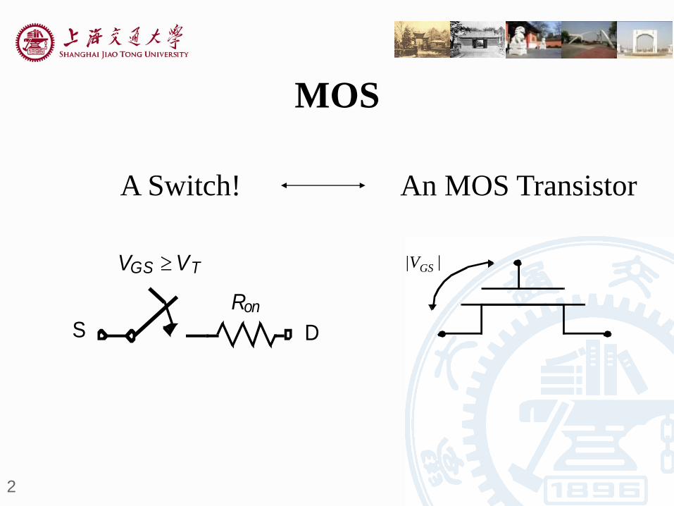
MOS
2
VGS VT
Ron
S D
A Switch!
|VGS |
An MOS Transistor
MOS
Static behavior
3
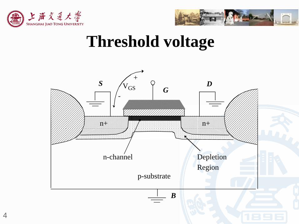
Threshold voltage
4
n+n+
p-substrate
DSG
B
VGS
+
-
Depletion
Region
n-channel

Body effect
5
Flat-band voltage
Substrate potential
2 SSB I
T ms F
ox ox ox
QQ QV
C C C
0
0
0
( 2 2 )
2
2
T T F SB F
B SS I
T ms F
ox ox ox
Si A
ox
V V V
with
Q Q QV
C C C
Q N
C
Surface Charge Implants
Body Effect
Coefficient
Workfunction
DifferenceDepletion
Layer Charge
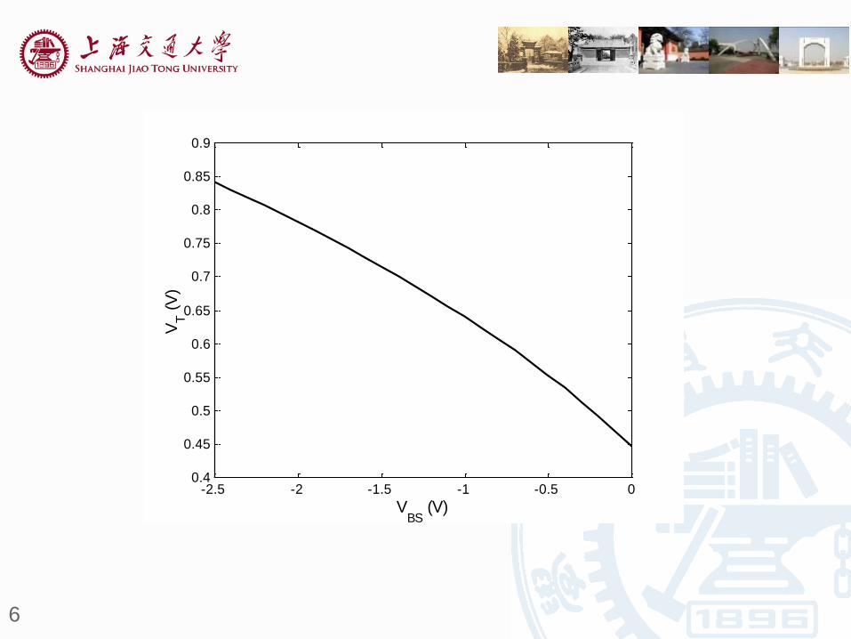
6
-2.5 -2 -1.5 -1 -0.5 00.4
0.45
0.5
0.55
0.6
0.65
0.7
0.75
0.8
0.85
0.9
VBS
(V)
VT (
V)

I-V characterisitcs
7
0 0.5 1 1.5 2 2.50
1
2
3
4
5
6x 10
-4
VDS (V)
I D(A
)
VGS= 2.5 V
VGS= 2.0 V
VGS= 1.5 V
VGS= 1.0 V
Resistive Saturation
VDS = VGS - VT
Quadratic
Relationship

Linear region(VDS<VGS-VT)
8
n+n+
p-substrate
D
S
G
B
VGS
xL
V(x)+–
VDS
ID
MOS transistor and its bias conditions
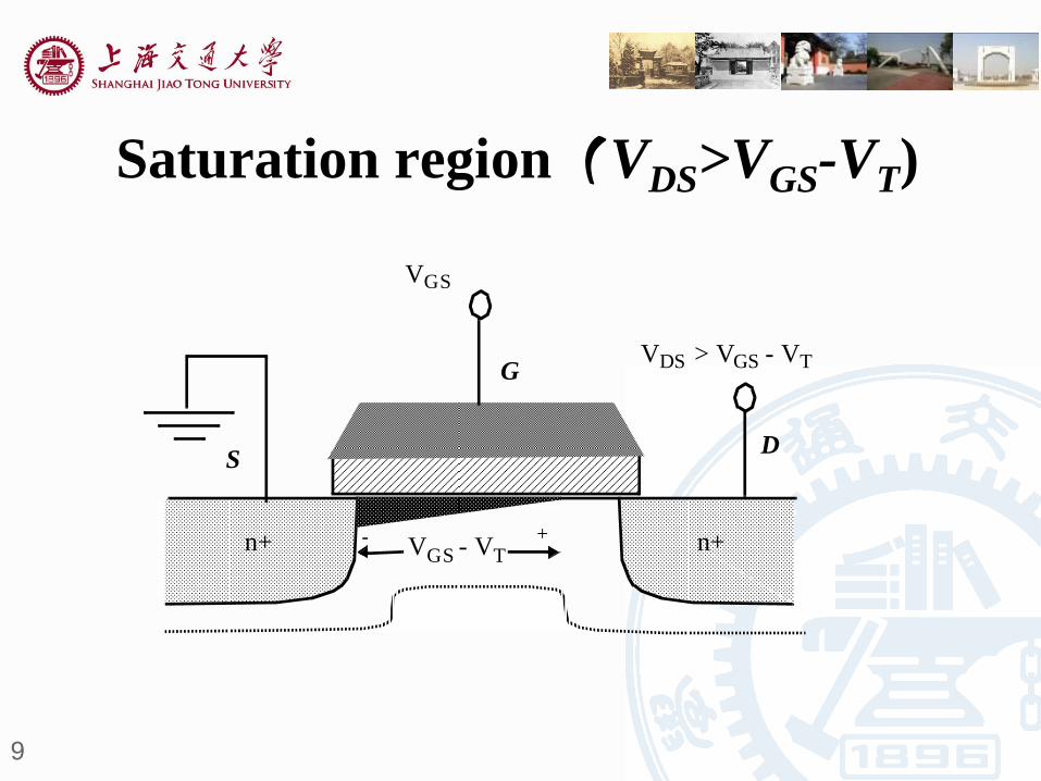
Saturation region(VDS>VGS-VT)
9
n+n+
S
G
VGS
D
VDS > VGS - VT
VGS - VT+-
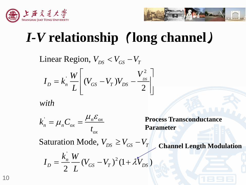
I-V relationship(long channel)
10
2
'
'
'
2
Linear Region,
( )2
Saturation Mode,
( ) (1 )2
DS
DS GS T
D n GS T DS
n ox
n n ox
ox
DS GS T
n
D GS T DS
V V V
VWI k V V V
L
with
k Ct
V V V
k WI V V V
L
Process Transconductance
Parameter
Channel Length Modulation
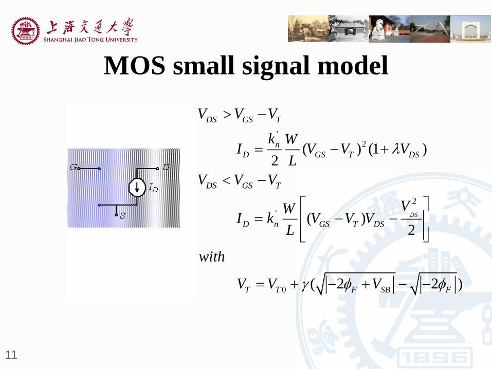
MOS small signal model
11
'
2
2
'
0
( ) (1 )2
( )2
( 2 2 )
DS
DS GS T
n
D GS T DS
DS GS T
D n GS T DS
T T F SB F
V V V
k WI V V V
L
V V V
VWI k V V V
L
with
V V V

12
Vgs
G
S
D
gmvgs ron
VDS>VGS-VT VDS<VGS-VT
DD
Don
Tgsm
IdV
dIr
VVkg
1)(
)(
1
1 1( ) [ ]
m DS
Don GS T DS
D
g kV
dIr k V V V
dV
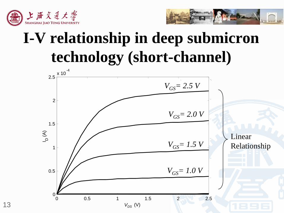
I-V relationship in deep submicron
technology (short-channel)
13
Linear
Relationship
-4
VDS (V)
0 0.5 1 1.5 2 2.50
0.5
1
1.5
2
2.5x 10
I D(A
)
VGS= 2.5 V
VGS= 2.0 V
VGS= 1.5 V
VGS= 1.0 V
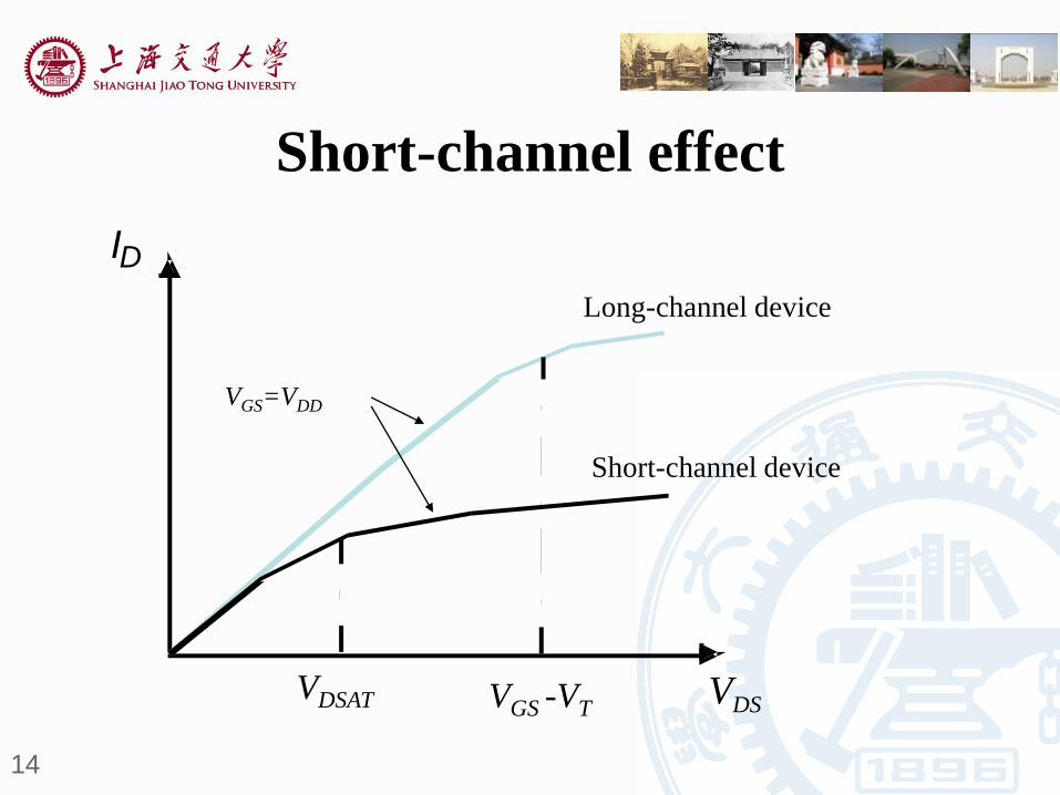
Short-channel effect
14
ID
Long-channel device
Short-channel device
VDSVDSAT VGS -VT
VGS=VDD

Velocity saturation Short-channel behavior: velocity saturation.
The velocity in long-channel device:
15
• The velocity in short-channel device:
The velocity is proportional to the electric field, and the
carrier mobility is a constant.
The continuity requirement between the two regions: 2 /c sat nv
1 / c
sat
v
v v
c
c
for
for
( )n n n
dVv x
dx

16
When the electrical field along the channel reaches a critical
value, the velocity of the carriers tends to saturate due to
scattering effects.
Fig Velocity-saturation

17
The drain current in the linear region for long-channel devices:
Replacing with n1 /
n
c
=> The drain current in the linear region for short-channel devices:
DSV
L
[ ]2
DSD n ox GS T DS
VWI C V V V
L
2
2
( )[( ) ]1 ( / ) 2
( )[( ) ] ( )2
n ox DS
D GS T DS
DS c
DS
n ox GS T DS DS
C VWI V V V
V L L
VWC V V V V
L
18
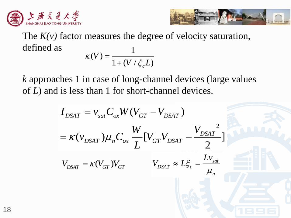
The K(v) factor measures the degree of velocity saturation,
defined as
k approaches 1 in case of long-channel devices (large values
of L) and is less than 1 for short-channel devices.
sat
DSAT c
n
LvV L
1( )
1 ( / )c
VV L
( )DSAT GT GTV V V
2
( )
( ) [ ]2
DSAT sat ox GT DSAT
DSAT
DSAT n ox GT DSAT
I v C W V V
VWv C V V
L
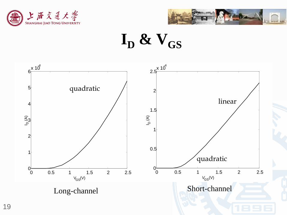
ID & VGS
19
0 0.5 1 1.5 2 2.50
1
2
3
4
5
6x 10
-4
VGS
(V)
I D(A
)
0 0.5 1 1.5 2 2.50
0.5
1
1.5
2
2.5x 10
-4
VGS
(V)
I D(A
)
quadratic
quadratic
linear
Long-channel Short-channel
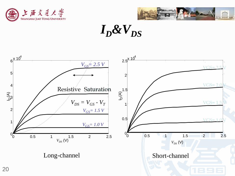
ID&VDS
20
-4
0 0.5 1 1.5 2 2.50
0.5
1
1.5
2
2.5x 10
I D(A
)
VGS= 2.5 V
VGS= 2.0 V
VGS= 1.5 V
VGS= 1.0 V
0 0.5 1 1.5 2 2.50
1
2
3
4
5
6x 10
-4
VDS (V)
I D(A
)
VGS= 2.5 V
VGS= 2.0 V
VGS= 1.5 V
VGS= 1.0 V
Resistive Saturation
VDS = VGS - VT
Long-channel Short-channel
VDS (V)
21
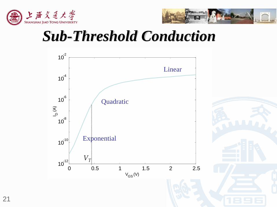
0 0.5 1 1.5 2 2.510
-12
10-10
10-8
10-6
10-4
10-2
VGS
(V)
I D(A
)
VT
Linear
Exponential
Quadratic
Sub-Threshold Conduction
22
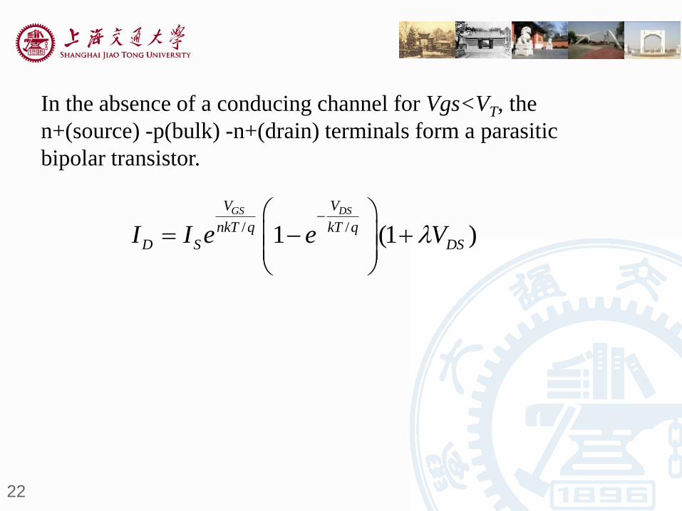
In the absence of a conducing channel for Vgs<VT, the
n+(source) -p(bulk) -n+(drain) terminals form a parasitic
bipolar transistor.
/ /1 (1 )GS DSV V
nkT q kT q
D S DSI I e e V
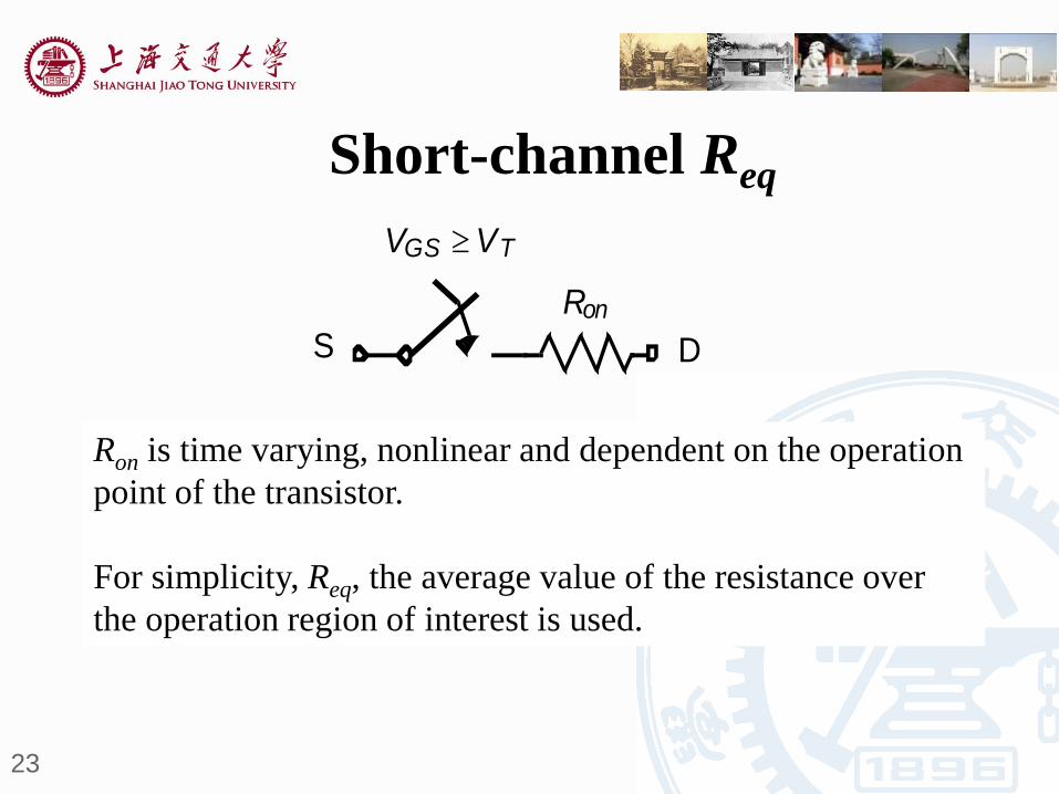
Short-channel Req
23
VGS VT
Ron
S D
Ron is time varying, nonlinear and dependent on the operation
point of the transistor.
For simplicity, Req, the average value of the resistance over
the operation region of interest is used.
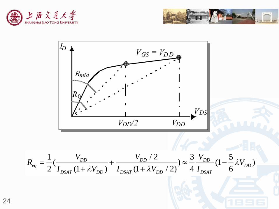
24
ID
VDS
VGS = VD D
VDD/2 VDD
R0
Rmid
/ 21 3 5( ) (1 )
2 (1 ) (1 / 2) 4 6
DD DD DD
eq DD
DSAT DD DSAT DD DSAT
V V VR V
I V I V I
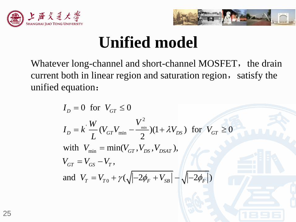
Unified model
25
Whatever long-channel and short-channel MOSFET,the drain
current both in linear region and saturation region,satisfy the
unified equation:
min
2
'
min
min
0
0 for 0
( )(1 ) for 02
with min( , , ),
,
and ( 2 2 )
D GT
D GT DS GT
GT DS DSAT
GT GS T
T T F SB F
I V
VWI k V V V V
L
V V V V
V V V
V V V
MOS
Dynamic behavior
26

MOS capacitance model
27
DS
G
B
CGDCGS
CSB CDBCGB

xd xd
L d
Polysilicon gate
Top view
Gate-bulkoverlap
Source
n+
Drain
n+
W
tox
n+ n+
Cross section
L
Gate oxide
gate capacitance
Cgso=Cgdo
=Cox×Ld×WLd
Leff=L-2×Ld
ox
gate
ox
C WLt

29
S D
G
CGC
S D
G
CGC
S D
G
CGC
Cut-off Resistive Saturation
The most important operation regions for digital ICs:saturation region and cutoff region
1. Cg
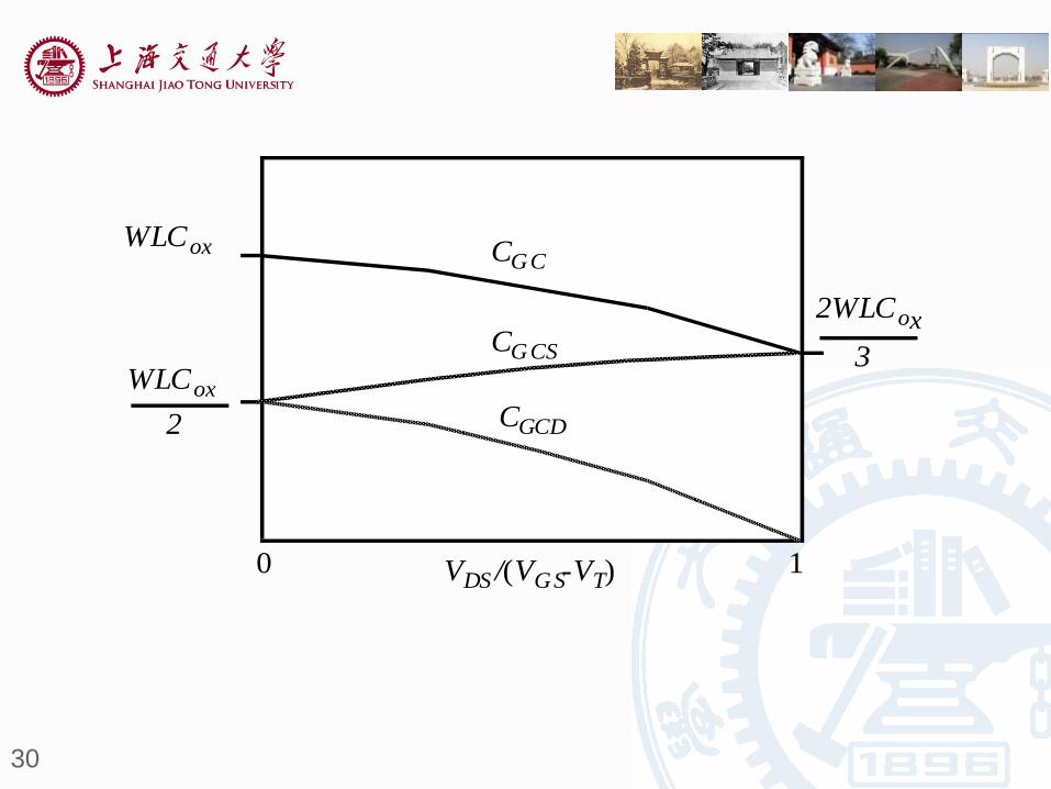
30
WLCox
WLCox
2
2WLCox
3
CGC
CGCS
VDS /(VGS-VT)
CGCD
0 1

31
Bottom
Side wall
Side wall
Channel
SourceN D
Channel-stop implantNA1
Substrate N A
W
xj
L S
2.Diffusion capacitance Cdiff
Cbottom: the
capacitance between
source/drain and
substrate;
Csw: the capacitance
between source/drain
and STI(shallow
trench isolation) 。
(2 )
diff bottom sw j jsw
j s jsw s
C C C C AREA C PERIMETER
C L W C L W

3.Total capacitance
CGS=Cgs+Cgso
Cgs=0 (cutoff)
= COX×W×Leff/2 (linear)
= COX×W×Leff(3/2) (saturation)
Cgso= Cox×xd×W
CGD=Cgd+Cgdo
Cgd=0 (cutoff )
= COX×W×Leff/2 (linear)
= 0 (saturation)
Cgdo= Cox×xd×W
32
CGB = COX × W × Leff (cutoff)
=0 (linear and saturation)
CSB=Csdiff
CDB=CDdiff
33
W
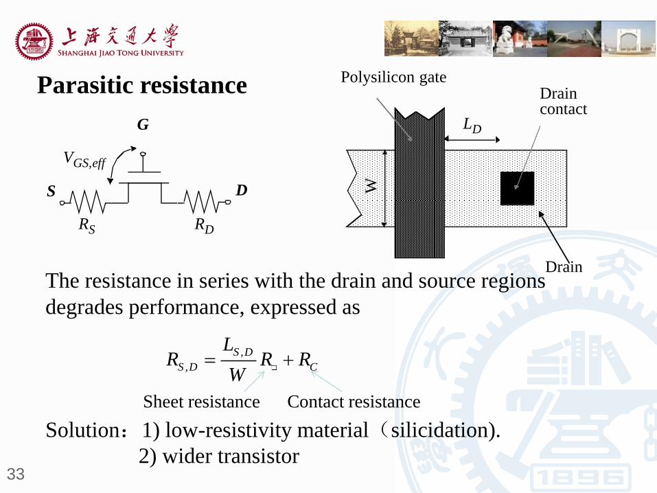
LD
Drain
Draincontact
Polysilicon gate
DS
G
RS RD
VGS,eff
Parasitic resistance
Solution:1) low-resistivity material(silicidation).
2) wider transistor
The resistance in series with the drain and source regions
degrades performance, expressed as
,
,
S D
S D C
LR R R
W
Sheet resistance Contact resistance
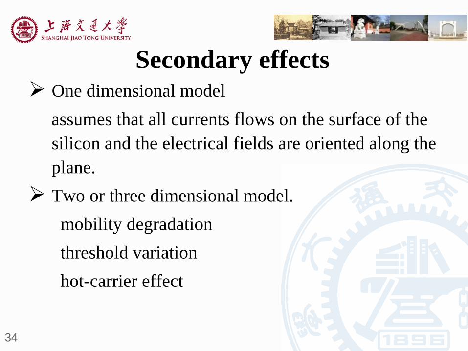
Secondary effects One dimensional model
assumes that all currents flows on the surface of the
silicon and the electrical fields are oriented along the
plane.
Two or three dimensional model.
mobility degradation
threshold variation
hot-carrier effect
34

Threshold voltage
35
DIBL: drain-induced barrier lowering, causes the threshold
potential as function of the operating points.
Raising the drain-source (bulk) voltage increases the width of
the drain-junction depletion region. Consequently, the threshold
decreases with increasing VDS.
Fig Threshold variations
(a) Threshold as a function
of the length (for low VDS)(b) Drain-induced barrier
lowering (for low L)
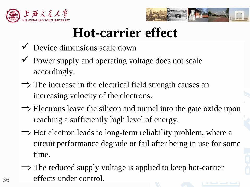
Hot-carrier effect Device dimensions scale down
Power supply and operating voltage does not scale
accordingly.
The increase in the electrical field strength causes an
increasing velocity of the electrons.
Electrons leave the silicon and tunnel into the gate oxide upon
reaching a sufficiently high level of energy.
Hot electron leads to long-term reliability problem, where a
circuit performance degrade or fail after being in use for some
time.
The reduced supply voltage is applied to keep hot-carrier
effects under control. 36
37
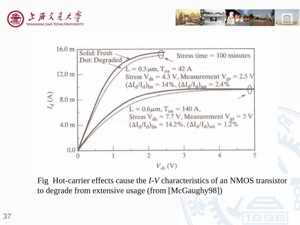
Fig Hot-carrier effects cause the I-V characteristics of an NMOS transistor
to degrade from extensive usage (from [McGaughy98])
38
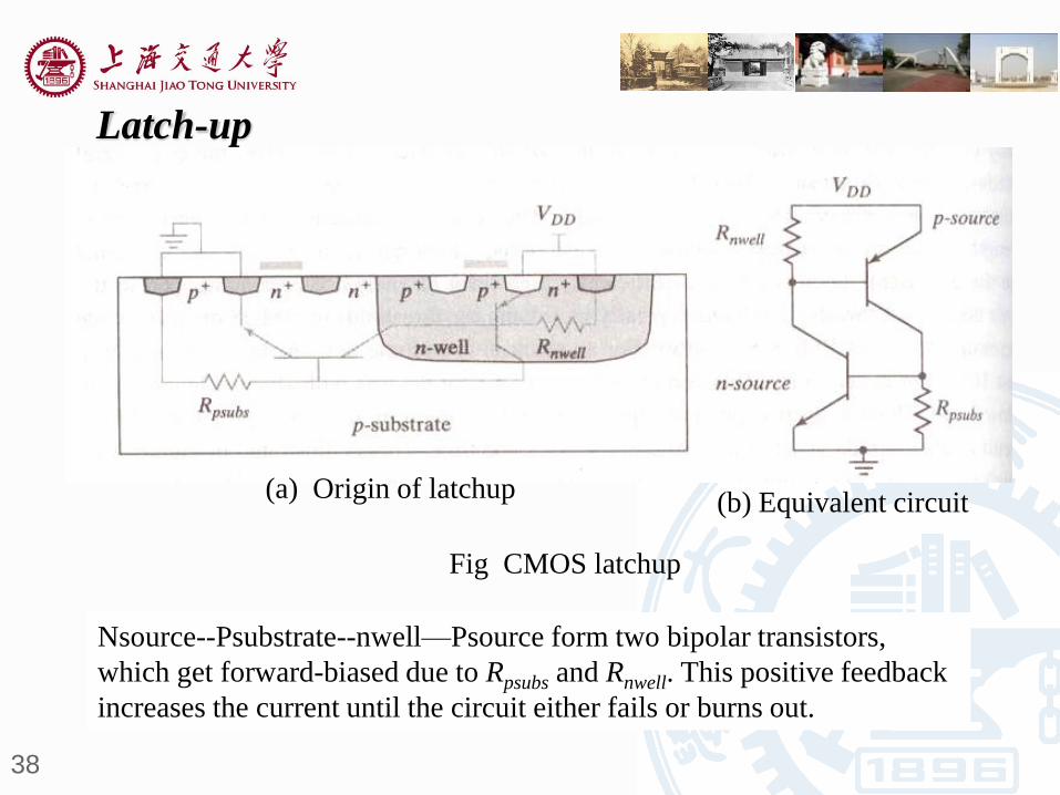
Latch-up
Nsource--Psubstrate--nwell—Psource form two bipolar transistors,
which get forward-biased due to Rpsubs and Rnwell. This positive feedback
increases the current until the circuit either fails or burns out.
Fig CMOS latchup
(b) Equivalent circuit(a) Origin of latchup

39
Solutions:
1) Place numerous well and substrate contacts
closer to the source connections.
2) Surround large-current device with guard rings:
reduce the resistance;
reduce the gain of the parasitic bipolars
3) SOI (Silicon on insulator) technology
SPICE MOSFET MODEL First-order model (Level 1)
-Accurate for long channel transistors (L>1 um)
-Suitable for manual analysis
Level-2 model
-Physically based model
-Not popular
Level-3 model
-Semiphysical model
-Parameters extracted by measurement 40

41
Table SPICE MOSFET MODEL PARAMETERS (PARTIAL LISTING)
42
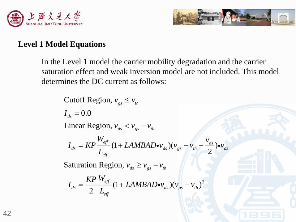
Level 1 Model Equations
In the Level 1 model the carrier mobility degradation and the carrier
saturation effect and weak inversion model are not included. This model
determines the DC current as follows:
2
Cutoff Region,
0.0
Linear Region,
(1 )( )2
Saturation Region,
(1 )( )2
gs th
ds
ds gs th
eff ds
ds ds gs th ds
eff
ds gs th
eff
ds ds gs th
eff
v v
I
v v v
W vI KP LAMBAD v v v v
L
v v v
WKPI LAMBAD v v v
L
43
The model calculates the effective channel length and width from the drawn
length and width as follows:
Effective Channel Length and Width
2( )
( 2 )
eff scaked scaled scaled scaled
eff scaled scaled scaled
L L LMLT XL LD DEL
W M W WMLT XW WD
1/2
1/2
1/2
1/2
,
0
( )
0
( 0.5 )
where the built-in voltage v is defined as:
th
sb
th bi sb
sb
sb
th bi
bi
bi fb
bi
Threshold Voltage v
v
v v GAMMA PHI v
v
vv v GAMMA PHI
PHI
v v PHI
or
v VTO GAMMA PHI

BSIM MODEL
BSIM 3V3 model is an industry wide standard for modeling
deep-submicron MOSFET transistors.
BSIM 3V3 model (denoted as Level 49) contains over 200
parameters. The majority parameters are related to the
modeling of second-order effects.
Documentation provided on the web site of
http://bwrc.eecs.berkeley.edu/IcBook.
44
45
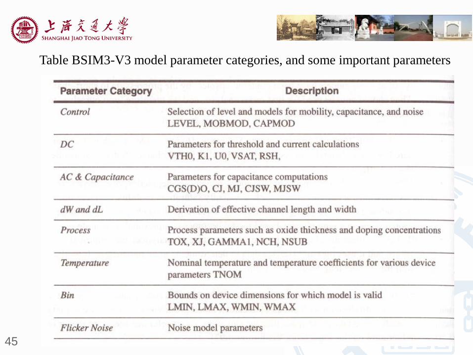
Table BSIM3-V3 model parameter categories, and some important parameters

46
Specifying MOSFET geometry in SPICE
Mname D G S B Modname L= W= AD= AS= PD= PS= NRD= NRS=
Mname : identifies the MOSFET
D: drain node
G: gate node
S: source node
B: bulk node
Modname: model for the transistor

47
Example:
(a) Layout and (b) cross section of CMOS

48
For n-channel and p-channel MOSFETS, the Level 1 SPICE models are:
.model MODN NMOS level=1 VTO=1 KP=50U LAMBDA=.033 GAMMA=.6
+ PHI=0.8 TOX=1.5E-10 CGDO=5E-10 CGSO=5E-10 CJ=1E-4 CJSW=5E-10
+ MJ=0.5 PB=0.95
.model MODP PMOS level=1 VTO=-1 KP=25U LAMBDA=.033 GAMMA=.6
+ PHI=0.8 TOX=1.5E-10 CGDO=5E-10 CGSO=5E-10 CJ=3E-4 CJSW=3.5E-10
+ MJ=0.5 PB=0.95
An n-channel MOSFET M1 with W=150um and L=3um has source and drain areas
and perimeters that are
AD=AS=9e-10 m2 and PD=PS=1.62e-4m
Transitory M1 is specified in SPICE by
M1 4 3 2 1 MODN W=150U L=3U AD=9E-10 AS=9E-10 PD=1.62E-4
+ PS=1.62E-4
where the drain is node 4, the gate is node 3, the source is node 2, and the bulk is node
1.


![Paper / Subject Code: 51402 / Logic Design Q.P. Code ...Evaluate using convolution theorem 1 22 ( 2) ( 4 8) s L ss ªº «»¬¼ [6] [b] Find bilinear transformation which maps the](https://img.pdfslide.us/doc/110x75/5e6dc311d4901450754dfe2d/paper-subject-code-51402-logic-design-qp-code-evaluate-using-convolution.jpg)


![International Research Journal of Engineering and Technology ...PSS considered [9]. It can be described as: U fd A ref pss fd A¬¼ ªº (12) E K V v u E T/ 2- DESIGN OF FUZZY LOGIC](https://img.pdfslide.us/doc/110x75/601252a357e27153ad03f627/international-research-journal-of-engineering-and-technology-pss-considered.jpg)
