Embed Size (px)
Citation preview

FULL PAPER
* E-mail: [email protected] (Mi-Kyung Han), [email protected] (Sung-Jin Kim), [email protected] (Wooyoung Lee); + These authors
equally contributed to this work. Received January 2, 2013; accepted February 24, 2013; published online XXXX, 2013. Chin. J. Chem. 2013, XX, 1—5 © 2013 SIOC, CAS, Shanghai, & WILEY-VCH Verlag GmbH & Co. KGaA, Weinheim 1
DOI: 10.1002/cjoc.201300006
Morphology Control of Bi2S3 Nanostructures and the Formation Mechanism
HeeJin Kim,a,b,+ Ji-eun Park,b,+ Kyung Kim,b Mi-Kyung Han,*,b Sung-Jin Kim,*,b and Wooyoung Lee*,a
a Department of Materials Science and Engineering, Yonsei University, Seoul 120-749, Korea b Department of Chemistry and Nano Science, Ewha Womans University, Seoul 120-750, Korea
Bismuthinite (Bi2S3) nanostructures were prepared by a hydrothermal method with sodium ethylenediamine-tetraacetate (EDTA-Na2). The morphology of Bi2S3 nanostructures was changed from a nanorod to a nanoplate by presence of the EDTA-Na2. The altered morphology was caused by the capping effect of EDTA-Na2 with Bi3+ ions, which induces the suboptimal growth direction due to partially blocking the preferential orientation direction. When the EDTA-Na2/Bi3+ molar ratio=1, the growth of Bi2S3 nanostructures was not allowed due to the chelating effect of EDTA-Na2. The obtained Bi2S3 nanorods, stacked nanorods, nanoplates and nanoparticles were characterized using X-ray diffraction (XRD), transmission electron microscopy (TEM), high-resolution transmission electron mi-croscopy (HRTEM) and selected area electron diffraction (SAED) pattern. A possible formation mechanism of these morphologies was proposed. The successful synthesis of various morphologies of nanostructured Bi2S3 may open up new possibilities for thermoelectric, electronic and optoelectronic uses of nanodevices based on Bi2S3
nanostructure.
Keywords bismuth sulfide (Bi2S3), hydrothermal, nanorod, nanoplate, thermoelectric material
Introduction AV
2BVI3 (A=Sb, Bi, As; B=S, Se, Te) group semi-
conductor compounds can be used in the applications of photoconducting targets, thermoelectric devices, elec-tronic and optoelectronic devices, and infrared (IR) spectroscopy.[1] Especially, Bi2S3 is useful as a material for photodiode arrays and photovoltaic converters due to its direct band gap (Eg) of 1.3 eV.[2,3] Bi2S3 is also used as a thermoelectric cooling material based on the Peltier effect.[4] Recently, many reports in a variety of journals have focused on 1-dimensional (1D), 2-dimen-sional (2D), and 3-dimensional (3D) crystalline Bi2S3 using various methods, such as solvothermal and hydro-thermal processes,[5-13] microwave synthesis,[14,15] ther-mal decomposition,[16-19] hot injection method,[20,21] tem-plate method,[22,23] single source precursor method,[24] and self-assembly method.[25-28]
Experimental conditions of solvothermal and hydro-thermal processes, such as a sulfur source, solvent type, and surfactant are important factors for controlling the morphology of Bi2S3 nanostructures.[9-13] For example, ultralong nanoribbons have been obtained using an NaOH and glycerol solution,[9] nanotubes were obtained using octadecylamine,[10] nanoribbons were obtained using three kinds of characteristic sulfur sources
(Na2S2O3, elemental S and Na2S),[11] superhydrophobic Bi2S3 complex nanostructures were obtained using bio-molecules (tripeptide glutathione (γ-Glu-Cys-Gly)),[12] and 3D Bi2S3 matlike architectures composed of assem-bled nanorods were obtained using seeded substrate.[13]
Especially, 3D Bi2S3 structures composed of 2D Bi2S3 have been focused on various applications, such as a hydrogen storage, high-energy batteries, and cata-lytic fields due to their unique structure and high surface area.[29] Most of these 3D structures are constituted of 1D or 2D nanostructures. Because of this, the control of Bi2S3 1D and 2D morphologies is very important. But, the simple control of Bi2S3 morphology still remains difficult due to a lack of comprehension of the aniso-tropic properties in the Bi2S3 structure.
In this paper, we reported on the morphological change of the Bi2S3 nanostructures by changing the mo-lar ratio of EDTA-Na2/Bi3+ without changing the sulfur source, solvent type, and surfactant. A variety of reports on the preparation of nanostructures using EDTA-Na2 were found in the literature involving α-Bi2O3,[30] YVO4,[31] CeVO4,[32] WO3,[33] LaVO4,[34] PbS[35] and ZnO[36] due to EDTA-Na2 behavior of chelating, cap-ping, and as a structure-directing effect. We suggested a possible control mechanism of Bi2S3 in regard to the

Kim et al.FULL PAPER
2 www.cjc.wiley-vch.de © 2013 SIOC, CAS, Shanghai, & WILEY-VCH Verlag GmbH & Co. KGaA, Weinheim Chin. J. Chem. 2013, XX, 1—5
role of the capping and chelating agent, EDTA-Na2. Our prepared products with variable morphologies via a hydrothermal process are still not reported in the litera-ture and might be useful for a thermoelectric, electronic, and optoelectronic devices to create functional nano-structured materials.
Experimental In a typical synthesis, 0.005 mol of Bi(NO3)3•5H2O
was dissolved in 20 mL water. The mixture was added to a 50 mL Teflon lined stainless steel autoclave, which was filled with a 20 mL of Na2S•9H2O (0.01 mol) aque-ous solution. EDTA-Na2 was added to the solution at four different molar ratio of EDTA-Na2/Bi3+ (0, 0.3, 0.7, or 1) in order to control the morphology of Bi2S3 nanostructures. The autoclave was maintained at a tem-perature of 120 ℃ for 24 h. During the reaction, the solution was stirred by a stainless steel stirrer with a rotational speed of 50 r/min. After the reaction, the autoclave was naturally cooled to room temperature. The powder (yield about 80%) was collected by filtra-tion, washed with deionized water, ethanol, and acetone several times and then dried at 60 ℃ for 12 h in a vacuum. The powder XRD patterns were collected on a Rigaku D/MAX X-ray (40 kV and 30 A) diffractometer with Cu Kα radiation (λ=1.54056 Å). The sample morphologies, fine structures, and SAED patterns were obtained by field emission transmission electron mi-croscopy (FE-TEM) using a model 2100F apparatus (JEOL, Tokyo, Japan).
Results and Discussion Figure 1 shows the XRD patterns of the final prod-
ucts. All diffraction peaks could be indexed to the pure orthorhombic phase of Bi2S3. The lattice constants cal-culated from the XRD pattern in Figures 1b-1e were about 11.151-11.171 Å, 11.301-11.331 Å, and 3.977-3.981 Å for the lattice parameter a, b, and c, respec-tively. The results showed good agreement with the JCPDS data (JCPDS 17-0320, a=11.149 Å, b=11.304 Å and c=3.981 Å). Peaks for bismuth, oxide, or other bismuth sulfide-oxide compounds did not appear in the diffraction patterns. From the XRD pattern, stacked nanorods, nanoplates, and nanoparticles (Figures 2c-2e) showed no significant deviation from that of calcu-lated Bi2S3. Enhanced (120) peak intensities in the XRD analysis were observed for the nanorod. The relative differences of peak intensity denoted a preferred crys-tallographic orientation. The above results indicated that the [00l] or [2 0]hk was the preferred orientation direc-tion of the Bi2S3 nanostructure without EDTA-Na2, but the preferred orientation plane disappeared by increas-ing the amount of EDTA-Na2. We confirmed the pre-ferred orientation direction of Bi2S3 nanorod by SAED pattern and HRTEM (Figure 2).
Figure 2 shows representative TEM images of Bi2S3
Figure 1 XRD patterns of powder products synthesized by hydrothermal method. (a) calculated Bi2S3, (b) without EDTA- Na2, (c) EDTA-Na2/Bi3+ molar ratio=0.3, (d) EDTA-Na2/Bi3+ molar ratio=0.7, (e) EDTA-Na2/Bi3+ molar ratio=1.
Figure 2 TEM and HRTEM images of powder product synthe-sized without EDTA-Na2. (a) TEM image of Bi2S3 nanorod, (b) HRTEM image of Bi2S3 nanorod, (c) SAED pattern of Bi2S3 nanorod, (d) schematic diagram of the preferential growth direc-tion.
nanorods prepared by the hydrothermal method without EDTA-Na2. Nanorods displayed a diameter of 10-30 nm and a length of 400-900 nm (Figure 2a). The chemical reactions in the hydrothermal synthesis could be expressed as follows:
2Bi(NO3)3 (aq)+3Na2S (aq) → Bi2S3 (s)+6NaNO3 (aq)
Bi2S3 nucleation → Bi2S3 nanowires
Bi3+ ions from Bi(NO3)3 react immediately with S2− ions from Na2S to form Bi2S3. The reaction solution changed color from clear to light gray immediately, in-dicating the formation of Bi2S3 nuclei. These freshly formed Bi2S3 nuclei in the solution grow into Bi2S3
Morphology Control of Bi2S3 Nanostructures and the Formation Mechanism
Chin. J. Chem. 2013, XX, 1—5 © 2013 SIOC, CAS, Shanghai, & WILEY-VCH Verlag GmbH & Co. KGaA, Weinheim www.cjc.wiley-vch.de 3
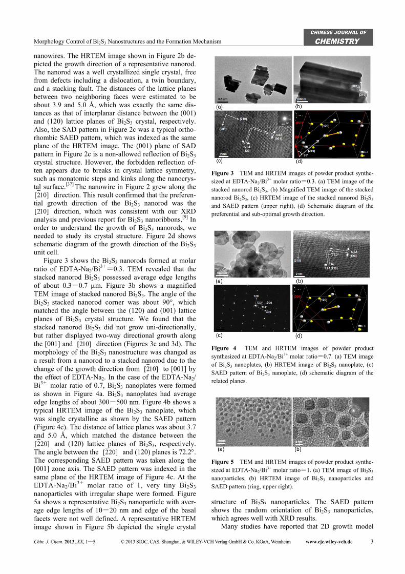
nanowires. The HRTEM image shown in Figure 2b de-picted the growth direction of a representative nanorod. The nanorod was a well crystallized single crystal, free from defects including a dislocation, a twin boundary, and a stacking fault. The distances of the lattice planes between two neighboring faces were estimated to be about 3.9 and 5.0 Å, which was exactly the same dis-tances as that of interplanar distance between the (001) and (120) lattice planes of Bi2S3 crystal, respectively. Also, the SAD pattern in Figure 2c was a typical ortho-rhombic SAED pattern, which was indexed as the same plane of the HRTEM image. The (001) plane of SAD pattern in Figure 2c is a non-allowed reflection of Bi2S3 crystal structure. However, the forbidden reflection of-ten appears due to breaks in crystal lattice symmetry, such as monatomic steps and kinks along the nanocrys-tal surface.[37] The nanowire in Figure 2 grew along the [210] direction. This result confirmed that the preferen-tial growth direction of the Bi2S3 nanorod was the [210] direction, which was consistent with our XRD analysis and previous report for Bi2S3 nanoribbons.[9] In order to understand the growth of Bi2S3 nanorods, we needed to study its crystal structure. Figure 2d shows schematic diagram of the growth direction of the Bi2S3 unit cell.
Figure 3 shows the Bi2S3 nanorods formed at molar ratio of EDTA-Na2/Bi3+=0.3. TEM revealed that the stacked nanorod Bi2S3 possessed average edge lengths of about 0.3-0.7 μm. Figure 3b shows a magnified TEM image of stacked nanorod Bi2S3. The angle of the Bi2S3 stacked nanorod corner was about 90°, which matched the angle between the (120) and (001) lattice planes of Bi2S3 crystal structure. We found that the stacked nanorod Bi2S3 did not grow uni-directionally, but rather displayed two-way directional growth along the [001] and [210] direction (Figures 3c and 3d). The morphology of the Bi2S3 nanostructure was changed as a result from a nanorod to a stacked nanorod due to the change of the growth direction from [210] to [001] by the effect of EDTA-Na2. In the case of the EDTA-Na2/ Bi3+ molar ratio of 0.7, Bi2S3 nanoplates were formed as shown in Figure 4a. Bi2S3 nanoplates had average edge lengths of about 300-500 nm. Figure 4b shows a typical HRTEM image of the Bi2S3 nanoplate, which was single crystalline as shown by the SAED pattern (Figure 4c). The distance of lattice planes was about 3.7 and 5.0 Å, which matched the distance between the [220] and (120) lattice planes of Bi2S3, respectively. The angle between the [220] and (120) planes is 72.2°. The corresponding SAED pattern was taken along the [001] zone axis. The SAED pattern was indexed in the same plane of the HRTEM image of Figure 4c. At the EDTA-Na2/Bi3+ molar ratio of 1, very tiny Bi2S3 nanoparticles with irregular shape were formed. Figure 5a shows a representative Bi2S3 nanoparticle with aver-age edge lengths of 10-20 nm and edge of the basal facets were not well defined. A representative HRTEM image shown in Figure 5b depicted the single crystal
Figure 3 TEM and HRTEM images of powder product synthe-sized at EDTA-Na2/Bi3+ molar ratio=0.3. (a) TEM image of the stacked nanorod Bi2S3, (b) Magnified TEM image of the stacked nanorod Bi2S3, (c) HRTEM image of the stacked nanorod Bi2S3 and SAED pattern (upper right), (d) Schematic diagram of the preferential and sub-optimal growth direction.
Figure 4 TEM and HRTEM images of powder product synthesized at EDTA-Na2/Bi3+ molar ratio=0.7. (a) TEM image of Bi2S3 nanoplates, (b) HRTEM image of Bi2S3 nanoplate, (c) SAED pattern of Bi2S3 nanoplate, (d) schematic diagram of the related planes.
Figure 5 TEM and HRTEM images of powder product synthe-sized at EDTA-Na2/Bi3+ molar ratio=1. (a) TEM image of Bi2S3 nanoparticles, (b) HRTEM image of Bi2S3 nanoparticles and SAED pattern (ring, upper right).
structure of Bi2S3 nanoparticles. The SAED pattern shows the random orientation of Bi2S3 nanoparticles, which agrees well with XRD results.
Many studies have reported that 2D growth model
Kim et al.FULL PAPER
4 www.cjc.wiley-vch.de © 2013 SIOC, CAS, Shanghai, & WILEY-VCH Verlag GmbH & Co. KGaA, Weinheim Chin. J. Chem. 2013, XX, 1—5
for Bi2S3 crystal structure, such as nanosheet and nano-plate, can be attributed to the anisotropic Bi-S atom chains structure of Bi2S3 unit cell[38] or the splitting crystal growth process.[39] In our work, in order to un-derstand the 2D growth of Bi2S3, we needed to know role of EDTA-Na2. EDTA-Na2 binds to Bi3+ ions through its two amines and four carboxylates.[40] In the absence of EDTA-Na2, Bi2S3 nanorods were formed along the [220] direction due to the intermolecular attraction between Bi and S atoms. However, in the presence of EDTA-Na2/Bi3+ molar ratio of 0.3 and 0.7, the 1D growth of the Bi2S3 nanostructures was prohib-ited and instead formed 2D growth like a nanoplate and a stacked nanorod. This remarkable change shows that EDTA-Na2 plays an important role in the morphology evolution. We propose that the formation of the 2D growth may result from the capping of Bi3+ ions with the EDTA-Na2 in the (120) plane, which gives rise to a prohibition of crystal growth along the [210] axis and inducement of crystal growth along the [001] direction. A similar morphological change of ZnO from nanowire to stacking nanoplates was reported in the presence of citrate as a complex agent,[41] which plays a similar role of EDTA-Na2 in our experiment. In the case of the EDTA-Na2/Bi3+ molar ratio of 1, we propose that EDTA-Na2 is fully prohibited to growth of Bi2S3 struc-ture. In aqueous solution with EDTA-Na2, EDTA-Na2 and Bi3+ react as follows:
Bi3++EDTA4− → (BiEDTA)−
(BiEDTA)− → Bi3++EDTA4−
Bi3++S2− → Bi2S3
Bi2S3 nucleation → Bi2S3 growth
EDTA-Na2 and Bi3+ can form very stable ligand
complex shown in the above reaction. The Bi3+ with EDTA-Na2 complex in aqueous solution proceeds with spontaneous nucleation and produces a number of nu-cleation. Then, Bi2S3 growth proceeds at very low rate due to the EDTA-Na2
complex. Therefore, only small Bi2S3 particles can be produced. In the case of the EDTA-Na2/Bi3+ molar ratio of 0.3 and 0.7, the capping effect of EDTA-Na2 is a more dominant factor than the chelating effect, which only affects the growth direction of Bi2S3 nanostructure. While the EDTA-Na2/Bi3+ mo-lar ratio increases by 1, the growth of Bi2S3 nanostruc-ture is fully restrained, thereby indicating that the che-lating effect of EDTA-Na2 is more dominant.
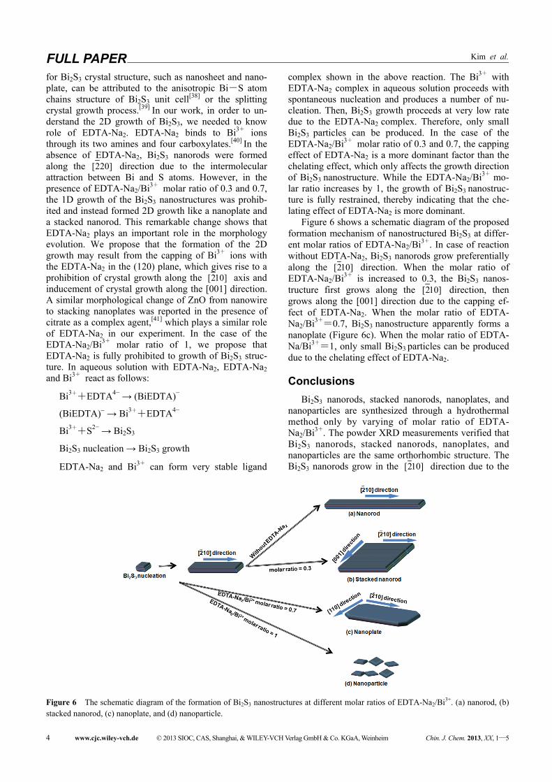
Figure 6 shows a schematic diagram of the proposed formation mechanism of nanostructured Bi2S3 at differ-ent molar ratios of EDTA-Na2/Bi3+. In case of reaction without EDTA-Na2, Bi2S3 nanorods grow preferentially along the [210] direction. When the molar ratio of EDTA-Na2/Bi3+ is increased to 0.3, the Bi2S3 nanos-tructure first grows along the [210] direction, then grows along the [001] direction due to the capping ef-fect of EDTA-Na2. When the molar ratio of EDTA- Na2/Bi3+=0.7, Bi2S3 nanostructure apparently forms a nanoplate (Figure 6c). When the molar ratio of EDTA- Na/Bi3+=1, only small Bi2S3 particles can be produced due to the chelating effect of EDTA-Na2.
Conclusions Bi2S3 nanorods, stacked nanorods, nanoplates, and
nanoparticles are synthesized through a hydrothermal method only by varying of molar ratio of EDTA- Na2/Bi3+. The powder XRD measurements verified that Bi2S3 nanorods, stacked nanorods, nanoplates, and nanoparticles are the same orthorhombic structure. The Bi2S3 nanorods grow in the [210] direction due to the
Figure 6 The schematic diagram of the formation of Bi2S3 nanostructures at different molar ratios of EDTA-Na2/Bi3+. (a) nanorod, (b) stacked nanorod, (c) nanoplate, and (d) nanoparticle.

Morphology Control of Bi2S3 Nanostructures and the Formation Mechanism
Chin. J. Chem. 2013, XX, 1—5 © 2013 SIOC, CAS, Shanghai, & WILEY-VCH Verlag GmbH & Co. KGaA, Weinheim www.cjc.wiley-vch.de 5
intermolecular attraction between Bi and S atoms. At the molar ratio of EDTA-Na2/Bi3+=0.3, stacked nano-rod Bi2S3 grow along the c axis direction instead of the [210] direction. The change of Bi2S3 morphology re-sults from the capping effect of Bi3+ ions with EDTA-Na2, which partially blocks the preferential ori-entation direction and also drives growth in the subop-timal orientation direction. When the EDTA-Na/Bi3+ molar ratio=1, the growth of Bi2S3 structure is not al-lowed due to the chelating effect of EDTA-Na2.
Acknowledgement W. Lee acknowledges for financial support by the
Priority Research Centers Program (2009-0093823) and Pioneer Research Center Program (2010-0019313) through the National Research Foundation of Korea (NRF). This research was supported by Nano-Material Technology Development Program through the National Research Foundation of Korea (NRF) funded by the Ministry of Education, Science and Technology (20110030147), National Research Foundation of Korea Grant funded by the Korean Government (20120000651).
References [1] Arivuoli, D.; Gnanam, F. D.; Ramasamy, P. J. Mater. Sci. Lett. 1988,
7, 711. [2] Mahapatra, P. K.; Roy, C. B. Sol. Cells 1983, 7, 225. [3] Nomura, R.; Kanaya, K.; Matsuda, H. Bull. Chem. Soc. Jpn. 1989,
62, 939. [4] Boudjouk, P.; Remington Jr, M. P.; Grier, D. G.; Jarabek, B. R.;
McCarthy, G. J. Inorg. Chem. 1998, 37, 35383. [5] Zhang, W. X.; Yang, Z. H.; Huang, X. M.; Zhang, S. Y.; Yu, W. C.;
Qian, Y. T.; Jia, Y. B.; Zhou, G. E.; Chen, L. Solid State Commun. 2001, 143, 119.
[6] Yu, S. H.; Qian, Y. T.; Shu, L.; Xie, Y.; Yang, L.; Wang, C. S. Ma-ter. Lett. 1998, 35, 116.
[7] Sheng, G. Z.; Chen, D.; Tang, K. B.; Li, F. Q.; Qian, Y. T. Chem. Phys. Lett. 2003, 370, 334.
[8] Wang, D. B.; Shao, M. W.; Yu, D. B.; Li, G. P.; Qian, Y. T. J. Cryst. Growth 2002, 243, 331.
[9] Liu, Z.; Peng, S.; Xie, Q.; Hu, Z.; Yang, Y.; Zhang, S.; Qian, Y. Adv. Mater. 2003, 15, 936
[10] Wang, D.; Hao, C.; Zheng, W.; Ma, X.; Chu, D.; Peng, Q.; Li, Y. Nano Res. 2009, 2, 130.
[11] Liu, Z.; Liang, J.; Li, S.; Peng, S.; Qian, Y. Chem. Eur. J. 2004, 10, 634.
[12] Xiao, Y.; Cao, H.; Liu, K.; Zhang, S.; Chernow, V. Nanotechnology
2010, 21, 145601. [13] Tang, C. J.; Zhang, Y. X.; Dou, X. C.; Li, G. H. J. Cryst. Growth
2010, 312, 692 [14] Thongtem, T.; Pilapong, C.; Kavinchan, J.; Phuruangrat, A.; Thong-
tem, S. J. Alloys Compd. 2010, 500, 195. [15] Tao, X.-C.; Shao, M.-W. Chin. J. Chem. 2002, 20, 1121. [16] Nomura, R.; Kanaya, K.; Matsuda, H. Bull. Chem. Soc. Jpn. 1989,
62, 939. [17] Larionov, S. V.; Patrina, L. A.; Uskov, E. M. Izv. Akad. Nauk SSSR,
Ser. Fiz 1979, 3, 94. [18] Popov, V. N.; Kolodezev, A. B.; Safonov, V. P.; Soveshch, T. D. V.
Tekhnol., Protsessy, Appar. Kach. Prom. Lyuminoforov. 1977, 98. [19] Cyganski, A.; Kobylecka, J. Thermochim. Acta 1981, 45, 65. [20] Malakooti, R.; Cademartiri, L.; Akçakir, Y.; Petrov, S.; Migliori, A.;
Ozin, G. A. Adv. Mater. 2006, 18, 2189. [21] Wu, T.; Zhou, X.; Zhang, H.; Zhong, X. Nano Res. 2010, 3, 379. [22] Li, L.; Sun, N.; Huang, Y.; Qin, Y.; Zhao, N.; Gao, J.; Li, M.; Zhou,
H.; Qi, L. Adv. Funct. Mater. 2008, 18, 1194. [23] Guo, C. F.; Cao, S.; Zhang, J.; Tang, H.; Guo, S.; Tian, Y.; Liu, Q. J.
Am. Chem. Soc. 2011, 133, 8211. [24] Song, C. X.; Wang, D. B.; Yang, T.; Hu, Z. S. Cryst. Eng. Comm.
2011, 13, 3087. [25] Cademartiri, L.; Guerin, G.; Bishop, K. J. M.; Winnik, M. A.; Ozin,
G. A. J. Am. Chem. Soc. 2012, 134, 9327. [26] Bishop, K. J. M.; Wilmer, C. E.; Soh, S.; Grzybowski, B. A. Small
2009, 5, 1600. [27] Nie, Z.; Petukhova, A.; Kumacheva, E. Nat. Nanotechnol. 2010, 5,
15. [28] Gao, Y.; Tang, Z. Small 2011, 7, 2133. [29] Jiang, J.; Gao, G.; Yu, R.; Qiu, G.; Liu, X. Solid State Sci. 2011, 13,
356. [30] Xiong, Y.; Wu, M. Z.; Ye, J.; Chen, Q. W. Mater. Lett. 2008, 62,
1165. [31] Ma, J.; Wu, Q. S.; Ding, Y. P. Mater. Lett. 2007, 61, 3616. [32] Luo, F.; Jia, C. J.; Song, W.; You, L. P.; Yan, C. H. Cryst. Growth
Des. 2005, 5, 137. [33] Ha, J.-H.; Muralidharan, P.; Kim, D. K. J. Alloys Compd. 2009, 475,
446. [34] Wang, N.; Chen, W.; Zhang, Q. F.; Dai, Y. Mater. Lett. 2008, 62,
109. [35] Zhou, S. M.; Feng, Y. S.; Zhang, L. D. J. Mater. Res. 2003, 18, 5. [36] Li, Z.; Fang, Y.; Peng, L.; Pan, D.; Wu, M. Cryst. Res. Technol.
2010, 10, 1083. [37] Čomor, M. I.; Dramićanin, M. D.; Rakočević, Z.; Zec, S.;
Nedeljković, J. M. J. Mater. Sci. Lett. 1998, 17, 1401. [38] Ye, C.; Meng, G.; Jiang, Z.; Wang, Y.; Wang, G.; Zhang, L. J. Am.
Chem. Soc. 2002, 124, 15180. [39] Han, Q. F.; Feng, S.; Sun, Y.; Wang, X.; Yang, X. J.; Lu, L. D. Ma-
ter. Lett. 2009, 63, 1611. [40] Kirchner, S. Inorganic Syntheses, McGraw-Hill, New York, 1957. [41] Cao, X. L.; Zeng, H. B.; Wang, M.; Xu, X. J.; Fang, M.; Ji, S. L.;
Zhang, L. D. J. Phys. Chem. C 2008, 112, 5267.
(Zhao, X.)


![3D Hierarchical Bi2S3 Nanostructures by ... · same hydrothermal method and assembled into the dye-sensitized solar cells with a good performance [32]. Chen et al. reported that they](https://img.pdfslide.us/doc/110x75/5e5c3777aa98c334433b8479/3d-hierarchical-bi2s3-nanostructures-by-same-hydrothermal-method-and-assembled.jpg)


![The prevalence of surface oxygen vacancies over the ...Nanocubes Nanostructures Crystal size Morphology Toluene Surface oxygen vacancies ... ity in zirconium-doped ceria [15]. However,](https://img.pdfslide.us/doc/110x75/5f1ea2eb43495322d6612a8a/the-prevalence-of-surface-oxygen-vacancies-over-the-nanocubes-nanostructures.jpg)