Embed Size (px)
Citation preview

IISW 2017, HIROSHIMA, JAPAN
MONOLITHIC NEAR INFRARED IMAGE SENSORS
ENABLED BY QUANTUM DOT PHOTODETECTOR
PAWEŁ E. MALINOWSKI, E. GEORGITZIKIS, J. MAES, M. MAMUN, O. ENZING, F. FRAZZICA,
J.VAN OLMEN, P. DE MOOR, P. HEREMANS, Z. HENS, AND D. CHEYNS
IISW 2017, HIROSHIMA, JAPAN2
IISW 2017, HIROSHIMA, JAPAN
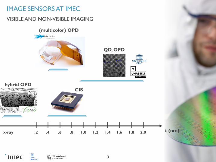
IMAGE SENSORS AT IMEC
3
VISIBLE AND NON-VISIBLE IMAGING
.2 .4 .6 .8 1.0 1.2 1.4 1.6 1.8 2.0
CIS
(multicolor) OPD
hybrid OPD
QD, OPD
x-ray λ (nm)
IISW 2017, HIROSHIMA, JAPAN
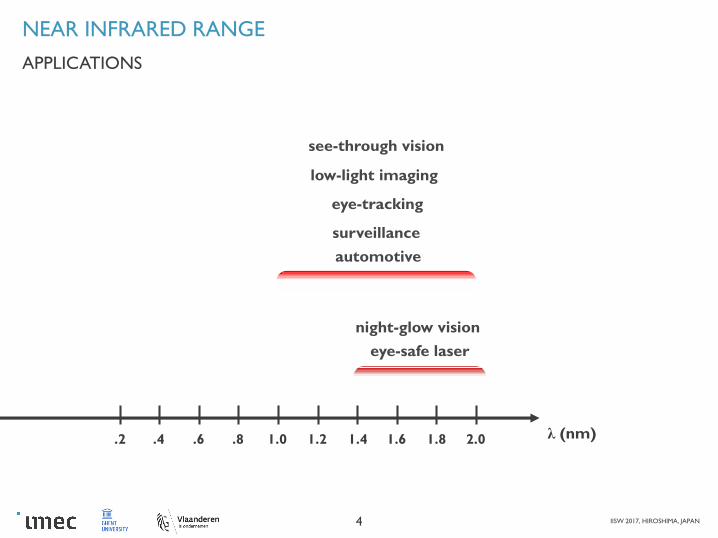
NEAR INFRARED RANGE
4
APPLICATIONS
.2 .4 .6 .8 1.0 1.2 1.4 1.6 1.8 2.0 λ (nm)
see-through vision
low-light imaging
eye-tracking
surveillance
automotive
night-glow vision
eye-safe laser
IISW 2017, HIROSHIMA, JAPAN
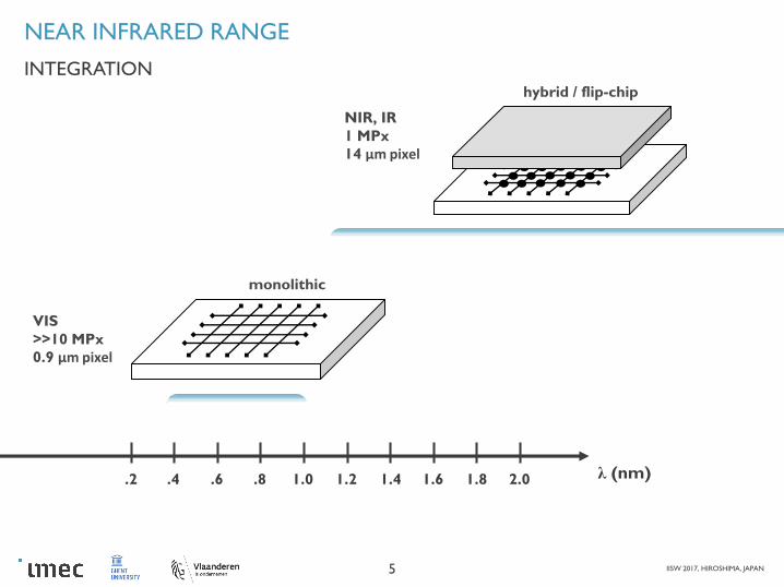
NEAR INFRARED RANGE
5
INTEGRATION
.2 .4 .6 .8 1.0 1.2 1.4 1.6 1.8 2.0 λ (nm)
monolithic
VIS
>>10 MPx
0.9 µm pixel
hybrid / flip-chip
NIR, IR
1 MPx
14 µm pixel
IISW 2017, HIROSHIMA, JAPAN
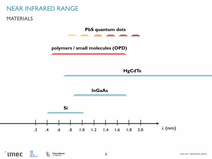
NEAR INFRARED RANGE
6
MATERIALS
.2 .4 .6 .8 1.0 1.2 1.4 1.6 1.8 2.0 λ (nm)
Si
InGaAs
HgCdTe
PbS quantum dots
polymers / small molecules (OPD)

IISW 2017, HIROSHIMA, JAPAN
NEAR INFRARED RANGE
7
INTEGRATION
.2 .4 .6 .8 1.0 1.2 1.4 1.6 1.8 2.0 λ (nm)
monolithic + QD
VIS, NIR, VIS+NIR
>1 MPx
<5 µm pixel

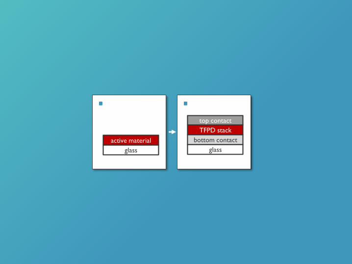
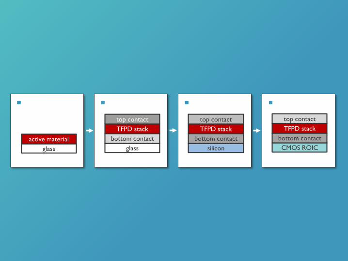
glass
active material
glass
bottom contact
TFPD stack
top contact
silicon
bottom contact
TFPD stack
top contact
CMOS ROIC
bottom contact
TFPD stack
top contact

glass
active material
IISW 2017, HIROSHIMA, JAPAN
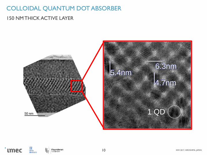
COLLOIDAL QUANTUM DOT ABSORBER
10
150 NM THICK ACTIVE LAYER
6.3nm
1 QD
5.4nm
4.7nm
glass
active material
glass
bottom contact
TFPD stack
top contact
IISW 2017, HIROSHIMA, JAPAN
PHOTODETECTOR STACK DEVELOPMENT
12
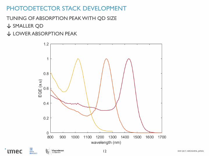
TUNING OF ABSORPTION PEAK WITH QD SIZE
↓ SMALLER QD
↓ LOWER ABSORPTION PEAK
IISW 2017, HIROSHIMA, JAPAN
PHOTODETECTOR STACK DEVELOPMENT
13
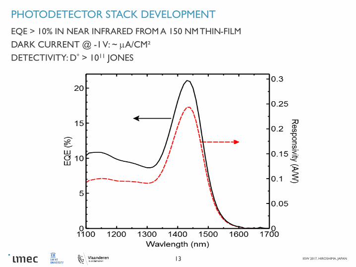
EQE > 10% IN NEAR INFRARED FROM A 150 NM THIN-FILM
DARK CURRENT @ -1 V: ~ A/CM²
DETECTIVITY: D* > 1011 JONES
IISW 2017, HIROSHIMA, JAPAN
PHOTODETECTOR STACK DEVELOPMENT
14
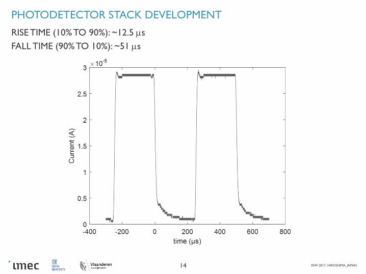
RISE TIME (10% TO 90%): ~12.5 s
FALL TIME (90% TO 10%): ~51 s

IISW 2017, HIROSHIMA, JAPAN
PHOTODETECTOR STACK DEVELOPMENT
15
PHOTO/DARK RATIO IMPROVEMENT AT LOW TEMPERATURE
193K PACKAGE AN OPTION FOR SPECIFIC APPLICATIONS
40 dB
63 dB
QDPD on glass, IR LED
IR LED illumination
dark

glass
active material
glass
bottom contact
TFPD stack
top contact
silicon
bottom contact
TFPD stack
top contact
IISW 2017, HIROSHIMA, JAPAN
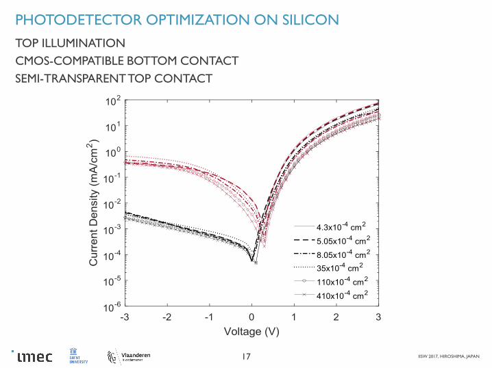
PHOTODETECTOR OPTIMIZATION ON SILICON
17
TOP ILLUMINATION
CMOS-COMPATIBLE BOTTOM CONTACT
SEMI-TRANSPARENT TOP CONTACT
IISW 2017, HIROSHIMA, JAPAN
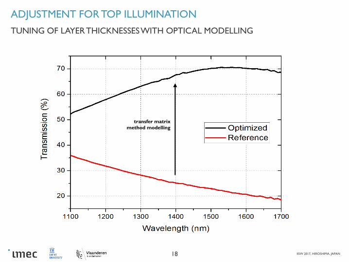
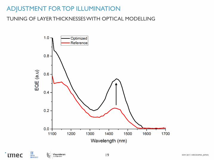
ADJUSTMENT FOR TOP ILLUMINATION
18
TUNING OF LAYER THICKNESSES WITH OPTICAL MODELLING
transfer matrix
method modelling
IISW 2017, HIROSHIMA, JAPAN
ADJUSTMENT FOR TOP ILLUMINATION
19
TUNING OF LAYER THICKNESSES WITH OPTICAL MODELLING
glass
active material
glass
bottom contact
TFPD stack
top contact
silicon
bottom contact
TFPD stack
top contact
CMOS ROIC
bottom contact
TFPD stack
top contact

IISW 2017, HIROSHIMA, JAPAN
OUTLOOK
• continuous screening of new materials
• main focus on quantum dots
• parallel tracks on OPD (polymers and small molecules)
• scaling up photodetector integration
• two options for the pixel array architecture:
• VIS+NIR in one plane (enabled by OPD patterning)
• monochrome NIR (towards 2 µm wavelength)
• dedicated readout circuit design and fabrication
• to be continued at IISW2019!
FROM PIXEL STACK TO MONOLITHIC INFRARED IMAGER

IISW 2017, HIROSHIMA, JAPAN
IISW 2017, HIROSHIMA, JAPAN
IMEC THIN-FILM PHOTODETECTOR TRACK RECORD
• P.E. Malinowski et al. „Monolithic Near Infrared Image Sensors Enabled by Quantum Dot Photodetector”, IISW 2017
• E. Georgitzikis et al., “Determining charge carrier extraction in lead sulfide quantum dot near infrared photodetectors”, SPIE Nanoscience + Engineering 2017
• D. Cheyns et al., “Infrared photodetectors based on lead-sulfide quantum dots”, MRS Spring 2017
• F. De Roose et al. „A Flexible Thin-Film Pixel Array with a Charge-to-Current Gain of 59μA/pC and 0.33% Nonlinearity and a Cost Effective Readout Circuit for Large-Area X-ray Imaging”, ISSCC2016
• G.H. Gelinck „X-Ray Detector-on-Plastic With High Sensitivity Using Low Cost, Solution-Processed Organic Photodiodes”, IEEE Transactions on Electron Devices 2016
• A. Kumar et al. „High performance x-ray imaging detectors on foil using solution-processed organic photodiodes with extremely low dark leakage current,” SPIE Organic Photonics + Electronics 2015
• F. De Roose et al. „Active Pixel Concepts for High-Resolution Large Area Imagers”, IISW 2015
• G.H. Gelinck et al. „Flexible X-ray detector with high sensitivity using low cost, solution-processed organic photodiodes,” IISW 2015
• P. E. Malinowski et al. „Organic Imager on Readout Backplane Based on TFTs With Cross-Linkable Dielectrics,” IEEE Photonics Technology Letters, 2014
• P. E. Malinowski et al. „Photolithographic patterning of organic photodetectors with a non-fluorinated photoresist system,” Organic Electronics 15 (10), 2014
• A. Kumar et al. „X-ray imaging sensor arrays on foil using solution processed organic photodiodes and organic transistors,” Proc. SPIE 9137, Organic Photonics VI, 2014
• G. H. Gelinck et al. „X-ray imager using solution processed organic transistor arrays and bulk heterojunction photodiodes on thin, flexible plastic substrate,” Organic Electronics 14 (10), 2013
• P. E. Malinowski et al. „Fully Organic Integrated Arrays on Flexible Substrates for X-Ray Imaging,” IISW 2013