Embed Size (px)
Citation preview
Monolithic Integration of Chip-scalePhotonic Networks in Si-CMOS
Mark BealsMIT Microphotonics Center
Microphotonics Center Spring MeetingApril 29, 2008
Acknowledgements
This work was sponsored by: Defense Advanced Research Projects Agency's (DARPA) EPIC and
UNIC programs supervised by Dr. Jagdeep Shah under contract no.HR0011-05-C-0027
- Andy Pomerene, Dan Carothers, Jim Beattie, Tim Conway, JosephGunta, Matthew Gregory, Craig Hill, Tom McIntyre, Vu A. Vu of BAESystems
- Douglas Gill, Sanjay Patel, Mahmud Rasras, Kun-Yi Tu, Y K Chen,Alice White of Alcatel Lucent Bell Laboratories
- Michael Watts, Sandia National Labs- Jim Psota, Jonathan Eaststep, Jason Miller, and Prof. Anant Agarwal
MIT CSAIL- Donghwan Ahn, Ching-yin Hong, Jifeng Liu, Jurgen Michel, Dan
Sparacin, Rong Sun, and Prof. Lionel Kimerling MIT EMat & MPC

Outline
Si CMOS Platform Photonic materials
- Silicon- Germanium
Active photonic devices- Detectors- Modulators
Chip-scale Photonic Network Summary
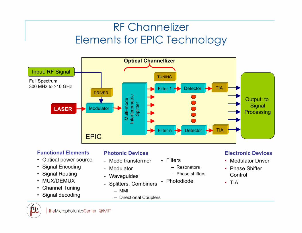
RF ChannelizerElements for EPIC Technology
Functional Elements• Optical power source• Signal Encoding• Signal Routing• MUX/DEMUX• Channel Tuning• Signal decoding
Photonic Devices- Mode transformer- Modulator- Waveguides- Splitters, Combiners
– MMI– Directional Couplers
Optical Channellizer
Modulator
Filter n
Detector
Detector
TIA
TIA
LASER
DRIVER
Input: RF Signal
Full Spectrum300 MHz to >10 GHz
TUNING
Filter 1
Mul
ti-m
ode
Inte
rfero
met
ricS
plitt
erEPIC
Output: to Signal
Processing
- Filters– Resonators– Phase shifters
- Photodiode
Electronic Devices• Modulator Driver• Phase Shifter
Control• TIA
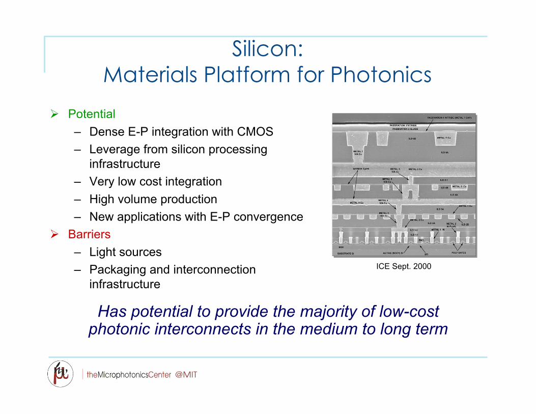
Silicon:Materials Platform for Photonics
Potential– Dense E-P integration with CMOS– Leverage from silicon processing
infrastructure– Very low cost integration– High volume production– New applications with E-P convergence
Barriers– Light sources– Packaging and interconnection
infrastructure
Has potential to provide the majority of low-costphotonic interconnects in the medium to long term
ICE Sept. 2000
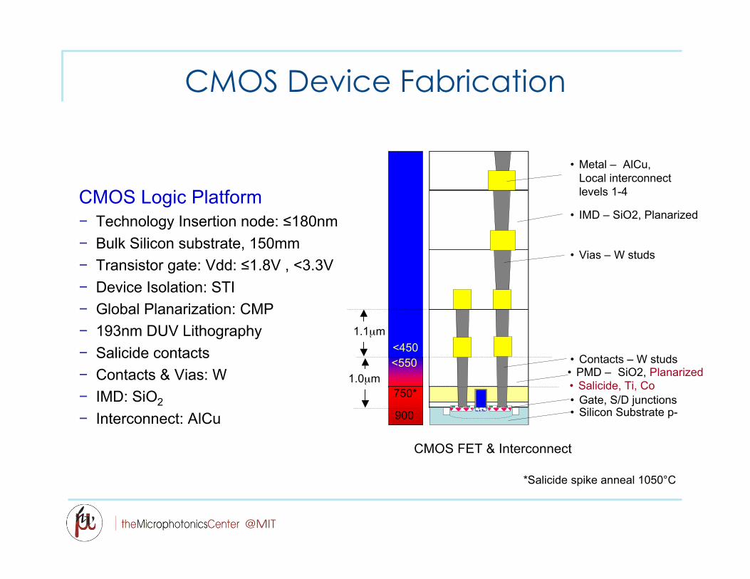
CMOS Device Fabrication
CMOS Logic Platform− Technology Insertion node: ≤180nm− Bulk Silicon substrate, 150mm− Transistor gate: Vdd: ≤1.8V , <3.3V− Device Isolation: STI− Global Planarization: CMP− 193nm DUV Lithography− Salicide contacts− Contacts & Vias: W− IMD: SiO2
− Interconnect: AlCu
• PMD – SiO2, Planarized1.0µm
1.1µm
CMOS FET & Interconnect
• Silicon Substrate p-• Gate, S/D junctions
• Metal – AlCu,Local interconnectlevels 1-4
• IMD – SiO2, Planarized
• Contacts – W studs
• Vias – W studs
900
<550<450
*Salicide spike anneal 1050°C
750*• Salicide, Ti, Co
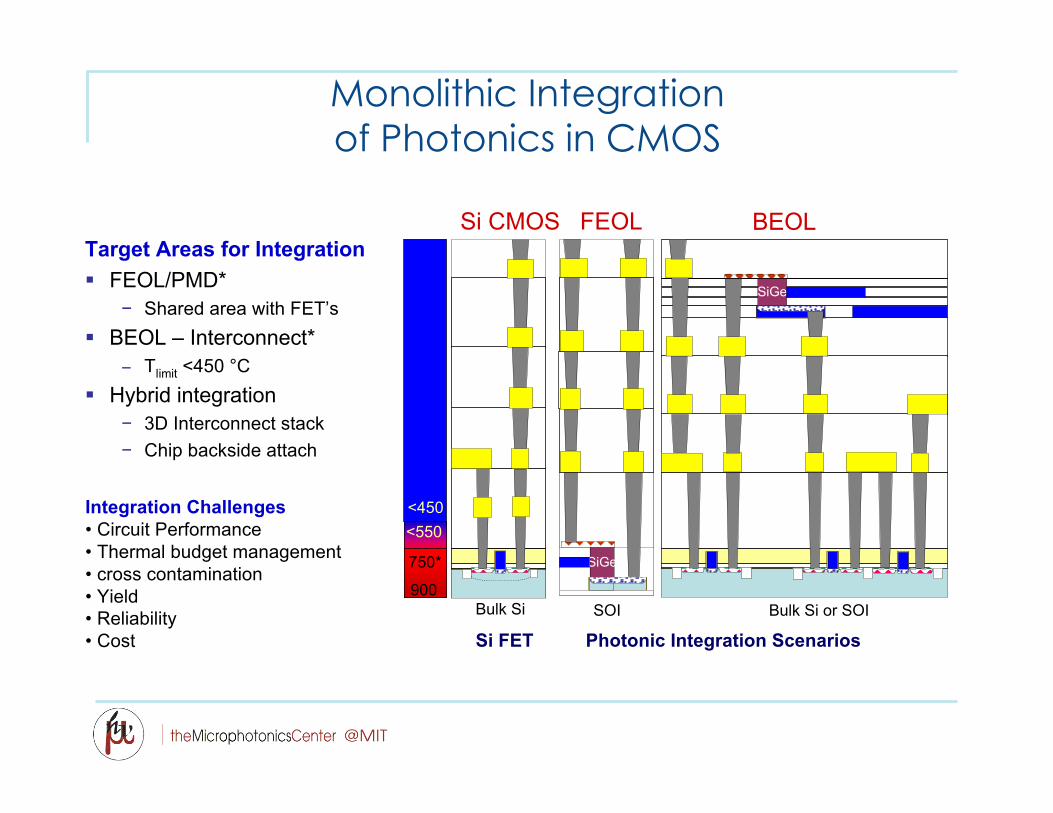
Monolithic Integrationof Photonics in CMOS
Target Areas for Integration FEOL/PMD*
− Shared area with FET’s BEOL – Interconnect*
− Tlimit <450 °C Hybrid integration
− 3D Interconnect stack− Chip backside attach
Si FET
900
<550<450
750*
Si CMOS
SiGe
FEOL
Photonic Integration Scenarios
Bulk Si SOI
SiGe
BEOL
Bulk Si or SOI
Integration Challenges• Circuit Performance• Thermal budget management• cross contamination• Yield• Reliability• Cost
Outline
Si CMOS Platform
Photonic Materials- Silicon
- Germanium
Active photonic devices- Detectors
- Modulators
Chip-scale Photonic Network
Summary
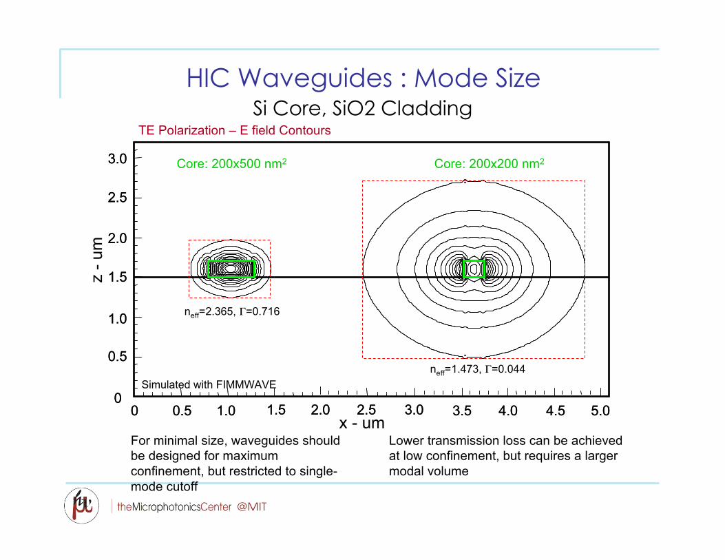
Lower transmission loss can be achievedat low confinement, but requires a largermodal volume
TE Polarization – E field ContoursSi Core, SiO2 Cladding
For minimal size, waveguides shouldbe designed for maximumconfinement, but restricted to single-mode cutoff
HIC Waveguides : Mode Size
Simulated with FIMMWAVE0
0.5
1.0
1.5
2.0
2.5
3.0
0 0.5 1.0 1.5 2.0 2.5 3.0 3.5 4.0 4.5 5.00
0.5
1.0
1.5
2.0
2.5
3.0
0 0.5 1.0 1.5 2.0 2.5 3.0 3.5 4.0 4.5
Core: 200x200 nm2
5.0
z - u
m
x - um
Core: 200x500 nm2
neff=2.365, Γ=0.716
neff=1.473, Γ=0.044
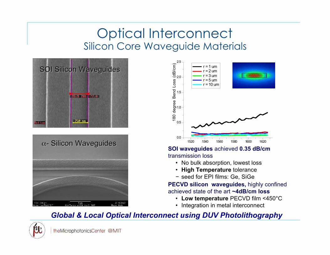
SOI waveguides achieved 0.35 dB/cmtransmission loss
• No bulk absorption, lowest loss• High Temperature tolerance− seed for EPI films: Ge, SiGe
PECVD silicon waveguides, highly confinedachieved state of the art ~4dB/cm loss
• Low temperature PECVD film <450°C• Integration in metal interconnect
Global & Local Optical Interconnect using DUV Photolithography
1520 1540 1560 1580 1600 1620 1640
0.0
0.5
1.0
1.5
2.0
2.5
18
0 d
eg
ree
Be
nd
Lo
ss (
dB
/cm
)
Wavelength (nm)
r = 1 um r = 2 um r = 3 um r = 5 um r = 10 um
Silicon Core Waveguide Materials
SOI Silicon WaveguidesSOI Silicon Waveguides
αα- Silicon Waveguides- Silicon Waveguides
Optical Interconnect
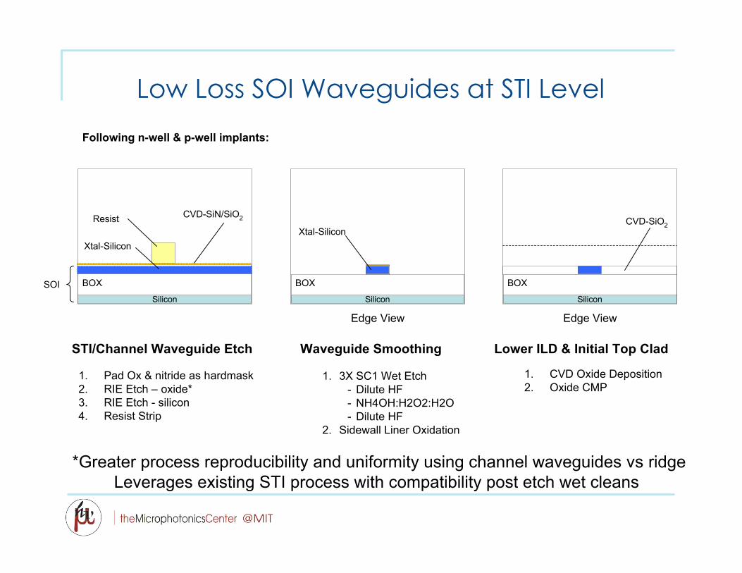
Low Loss SOI Waveguides at STI Level
SOISilicon
BOX
Xtal-Silicon
CVD-SiN/SiO2
Silicon
Edge View
BOX
CVD-SiO2
1. Pad Ox & nitride as hardmask2. RIE Etch – oxide*3. RIE Etch - silicon4. Resist Strip
1. 3X SC1 Wet Etch- Dilute HF- NH4OH:H2O2:H2O- Dilute HF
2. Sidewall Liner Oxidation
Waveguide SmoothingSTI/Channel Waveguide Etch Lower ILD & Initial Top Clad
1. CVD Oxide Deposition2. Oxide CMP
Silicon
Edge View
BOX
Xtal-Silicon
Following n-well & p-well implants:
Resist
*Greater process reproducibility and uniformity using channel waveguides vs ridgeLeverages existing STI process with compatibility post etch wet cleans
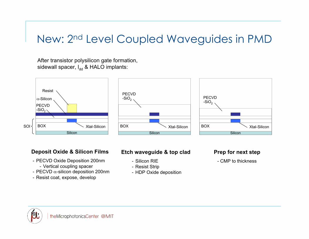
New: 2nd Level Coupled Waveguides in PMD
Silicon
SOI BOX Xtal-Silicon
PECVD-SiO2
Deposit Oxide & Silicon Films- PECVD Oxide Deposition 200nm
- Vertical coupling spacer- PECVD α-silicon deposition 200nm- Resist coat, expose, develop
α-Silicon
After transistor polysilicon gate formation,sidewall spacer, ldd & HALO implants:
Silicon
BOX Xtal-Silicon
PECVD-SiO2
Etch waveguide & top clad- Silicon RIE- Resist Strip- HDP Oxide deposition
Silicon
BOX Xtal-Silicon
PECVD-SiO2
Prep for next step- CMP to thickness
Resist
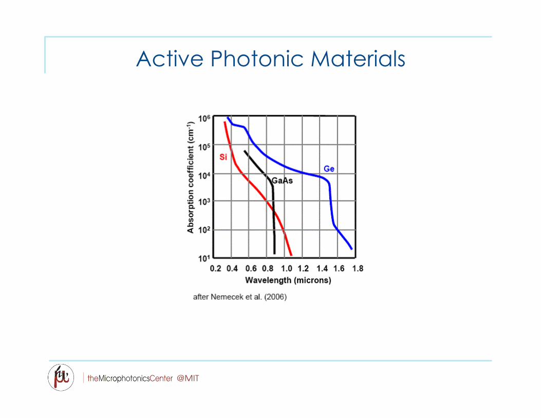
Active Photonic Materials

Ge Detector Designs
• Graded buffer layer growth+ Low dislocation density (~106 cm-1)- Thick buffer (1µm) – difficult integration- Absorption in buffer leads to diffusion tail- Integration with waveguides difficult
• GeOI+ Very low dislocation density- Requires ultra-thin SOI or wafer bonding- Integration with waveguides difficult
Samavedam, et al.
Koester, et al.
• Ge-directly-on-Si+ Flexible growth conditions+ SOI compatible+ Easy integration with waveguides- Dislocation density ~ 107 cm-1
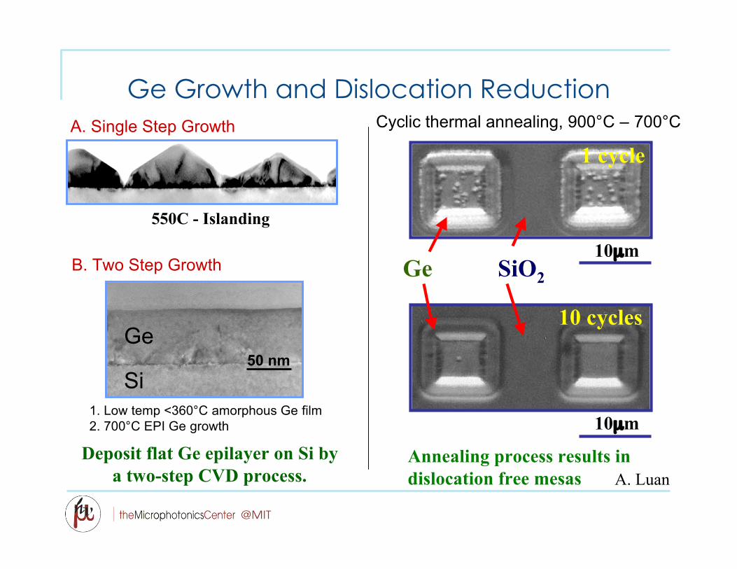
Ge Growth and Dislocation Reduction
A. LuanDeposit flat Ge epilayer on Si by
a two-step CVD process.
10µm
10 cycles
Annealing process results indislocation free mesas
10µmGe SiO2
1 cycleCyclic thermal annealing, 900°C – 700°C
550C - Islanding
A. Single Step Growth
50 nmGe
Si1. Low temp <360°C amorphous Ge film2. 700°C EPI Ge growth
B. Two Step Growth
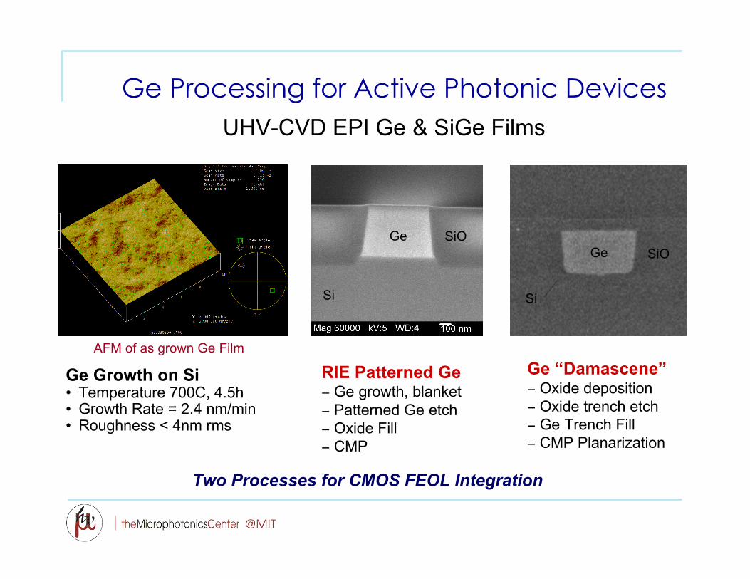
Ge Processing for Active Photonic Devices
Ge Growth on Si• Temperature 700C, 4.5h• Growth Rate = 2.4 nm/min• Roughness < 4nm rms
UHV-CVD EPI Ge & SiGe Films
AFM of as grown Ge Film
RIE Patterned Ge− Ge growth, blanket− Patterned Ge etch− Oxide Fill− CMP
Ge “Damascene”− Oxide deposition− Oxide trench etch− Ge Trench Fill− CMP Planarization
Two Processes for CMOS FEOL Integration
Ge SiO
Si
Ge SiO
Si
Outline
Si CMOS Platform Photonic Materials
- Silicon- Germanium
Active photonic devices- Detectors- Modulators
Chip-scale Photonic Network Summary
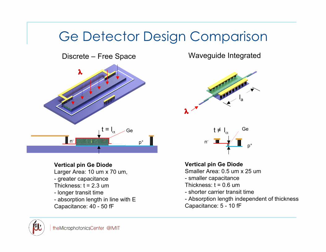
Ge Detector Design ComparisonDiscrete – Free Space
Vertical pin Ge DiodeLarger Area: 10 um x 70 um, - greater capacitanceThickness: t = 2.3 um - longer transit time- absorption length in line with ECapacitance: 40 - 50 fF
λ
n- p+
Ge
i
Waveguide Integrated
Vertical pin Ge DiodeSmaller Area: 0.5 um x 25 um- smaller capacitanceThickness: t = 0.6 um- shorter carrier transit time- Absorption length independent of thicknessCapacitance: 5 - 10 fF
Ge
n-
p+
λ
t = lα t ≠ lα
la
Freespace” Ge Diode Performance
600 800 1000 1200 1400 1600 1800
0.0
0.2
0.4
0.6
0.8
1.0
1.2 Ideal Responsivity
Resp
onsi
vit
y (
A/W
)
Wavelength (nm)
-2V 0V
0.01 0.1 1 10-3
-2
-1
0
f3dB
=8
.5G
Hz
0 1 2 3 40
2
4
6
8
10
3dB
Ban
dw
idth
(G
Hz)
Reverse Bias (V)No
rmal
ized
Res
po
nse
(d
B)
Frequency (GHz)
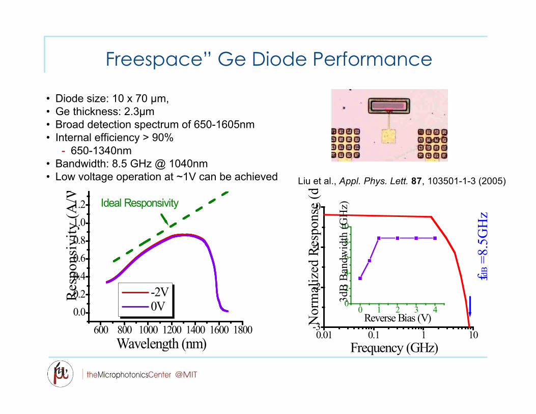
Liu et al., Appl. Phys. Lett. 87, 103501-1-3 (2005)
• Diode size: 10 x 70 µm, • Ge thickness: 2.3µm• Broad detection spectrum of 650-1605nm • Internal efficiency > 90%
- 650-1340nm• Bandwidth: 8.5 GHz @ 1040nm• Low voltage operation at ~1V can be achieved
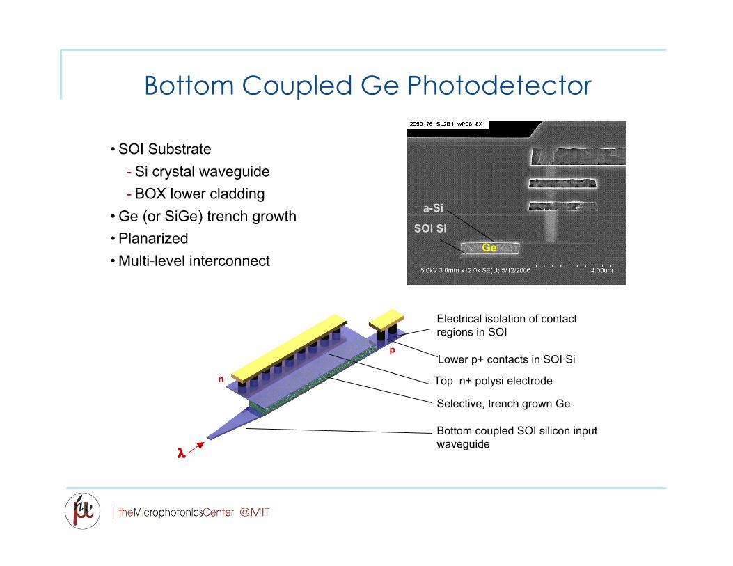
Bottom Coupled Ge Photodetector
Bottom coupled SOI silicon inputwaveguide
Electrical isolation of contactregions in SOI
Top n+ polysi electrode
Selective, trench grown Ge
• SOI Substrate- Si crystal waveguide- BOX lower cladding
• Ge (or SiGe) trench growth• Planarized• Multi-level interconnect
Lower p+ contacts in SOI Sip
n
λ
GeSOI Si
a-Si

Bottom Coupled Ge-0.8% Si pin Detector
1480 1500 1520 1540 1560
0.10
0.12
0.14
0.16
0.18
0.20
0.22
0.24
20 µm
5 µm
Res
po
nsi
vit
y (
A/W
)
Wavelength (nm)1000 1500 2000
0.0
2.0m
4.0m
6.0m
8.0m
0.01 0.1 1 10-30
-25
-20
-15
-10
-5
0
RF
res
ponse
(dB
)
Frequency (GHz)Photo
resp
onse
(V
)
Time (psec)
D. Ahn, MITLEOS 2006
3dB Bandwidth ~1.5 GHz- RC delay limited- High series resistance of
device contacts
Direct bandgap forGe-0.8% Si is 1520nm
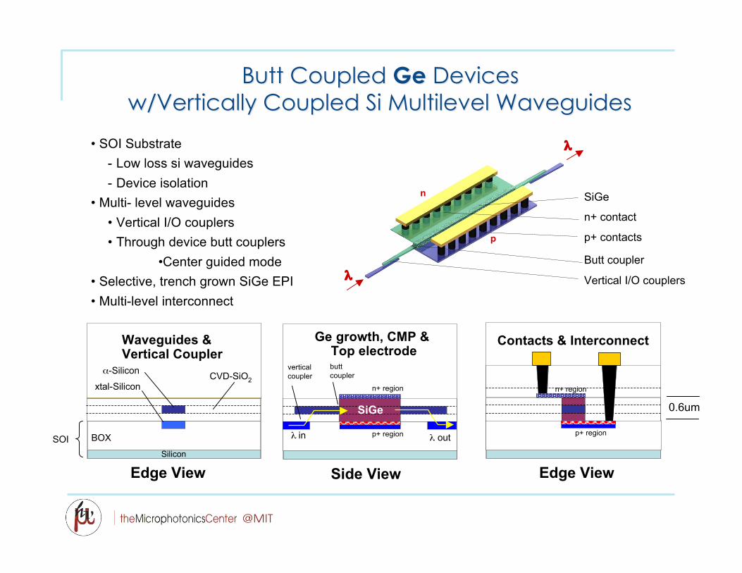
Butt Coupled Butt Coupled GeGe Devices Devicesw/Vertically Coupled Si Multilevel Waveguidesw/Vertically Coupled Si Multilevel Waveguides
Edge ViewSilicon
Waveguides & Vertical Coupler
α-Silicon
SOI BOX
xtal-SiliconCVD-SiO2
Side View
λ in λ out
SiGe
Ge growth, CMP & Top electrode
verticalcoupler
buttcoupler
p+ region
n+ region
• SOI Substrate- Low loss si waveguides- Device isolation
• Multi- level waveguides• Vertical I/O couplers• Through device butt couplers
•Center guided mode• Selective, trench grown SiGe EPI• Multi-level interconnect
Vertical I/O couplers
n+ contact
p+ contacts
SiGe
p
n
λ
λ
Butt coupler
Edge View
Contacts & Interconnect
p+ region
n+ region
0.6um
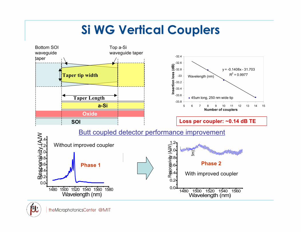
Si WG Vertical CouplersSi WG Vertical CouplersBottom SOIwaveguidetaper
Taper tip width
Taper Length
Top a-Siwaveguide taper
SOI Oxide
a-Si
Loss per coupler: ~0.14 dB TE
1480 1500 1520 1540 15600.0
0.2
0.4
0.6
0.8
1.0
1.2
1 2 3 4 5 6-60
-50
-40
-30
-20
Detector bandwith>4.5GHz
Roll off due to thelimitation of TIA
RF
Pow
er
(dB
m)
RF Frequency (GHz)
Re
spo
nsi
vity
(A
/W)
Wavelength (nm)1480 1500 1520 1540 1560 1580
0.0
0.2
0.4
0.6
0.8
1.0
1.2
1.4 Ideal Responsivity
Re
sp
on
siv
ity (
A/W
)
Wavelength (nm)
a-Si waveguide butt-coupled 50µm SiGe detector
Butt coupled detector performance improvement
Without improved coupler
With improved coupler
y = -0.1408x - 31.703
R2 = 0.9977
-33.8
-33.6
-33.4
-33.2
-33
-32.8
-32.6
-32.4
5 6 7 8 9 10 11 12 13 14 15
Number of couplers
Insert
ion
lo
ss (
dB
)
45um long, 250 nm wide tip
Wavelength (nm)
Phase 1 Phase 2
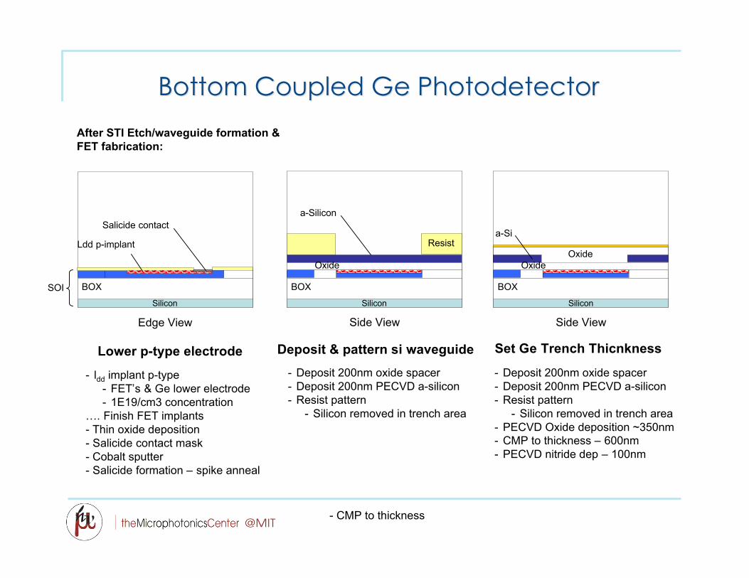
Bottom Coupled Bottom Coupled GeGe Photodetector Photodetector
Silicon
Edge View
SOI BOX
Ldd p-implant
Lower p-type electrode
- ldd implant p-type- FET’s & Ge lower electrode- 1E19/cm3 concentration
…. Finish FET implants- Thin oxide deposition- Salicide contact mask- Cobalt sputter- Salicide formation – spike anneal
Salicide contact
After STI Etch/waveguide formation &FET fabrication:
- CMP to thickness
Silicon
Side View
BOX
a-Silicon
Deposit & pattern si waveguide- Deposit 200nm oxide spacer- Deposit 200nm PECVD a-silicon- Resist pattern
- Silicon removed in trench area
Resist
Oxide
Silicon
Side View
BOX
a-Si
- Deposit 200nm oxide spacer- Deposit 200nm PECVD a-silicon- Resist pattern
- Silicon removed in trench area- PECVD Oxide deposition ~350nm- CMP to thickness – 600nm - PECVD nitride dep – 100nm
OxideOxide
Set Ge Trench Thicnkness
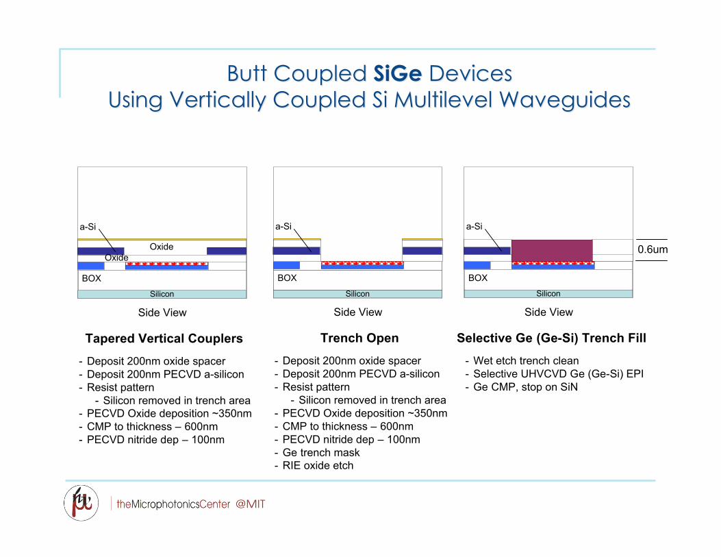
Butt Coupled Butt Coupled SiGeSiGe Devices DevicesUsing Vertically Coupled Si Multilevel WaveguidesUsing Vertically Coupled Si Multilevel Waveguides
- Deposit 200nm oxide spacer- Deposit 200nm PECVD a-silicon- Resist pattern
- Silicon removed in trench area- PECVD Oxide deposition ~350nm- CMP to thickness – 600nm - PECVD nitride dep – 100nm
Silicon
Side View
BOX
a-Si
OxideOxide
Tapered Vertical Couplers
Silicon
Side View
BOX
a-Si
- Deposit 200nm oxide spacer- Deposit 200nm PECVD a-silicon- Resist pattern
- Silicon removed in trench area- PECVD Oxide deposition ~350nm- CMP to thickness – 600nm - PECVD nitride dep – 100nm- Ge trench mask- RIE oxide etch
Trench Open
Silicon
Side View
BOX
a-Si
- Wet etch trench clean- Selective UHVCVD Ge (Ge-Si) EPI- Ge CMP, stop on SiN
Selective Ge (Ge-Si) Trench Fill
0.6um
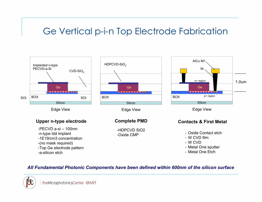
GeGe Vertical Vertical p-i-np-i-n Top Electrode Fabrication Top Electrode Fabrication
SOISilicon
Edge View
BOX
CVD-SiO2
Upper n-type electrode-PECVD a-si – 100nm-n-type ldd implant -1E19/cm3 concentration-(no mask required)-Top Ge electrode pattern-a-silicon etch
1.0um
Implanted n-typePECVD-a-Si
SOISilicon
Edge View
BOX
Complete PMD
-HDPCVD SiO2-Oxide CMP
HDPCVD-SiO2
Contacts & First Metal
- Oxide Contact etch- W CVD film- W CVD- Metal One sputter- Metal One Etch
Silicon
Edge View
BOX
AlCu M1
p+ region
n+ region
W
GeGeGe
All Fundamental Photonic Components have been defined within 600nm of the silicon surface
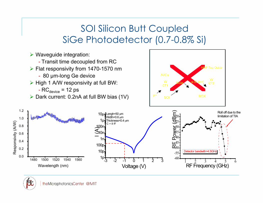
Waveguide integration:- Transit time decoupled from RC
Flat responsivity from 1470-1570 nm- 80 µm-long Ge device
High 1 A/W responsivity at full BW:- RCdevice = 12 ps
Dark current: 0.2nA at full BW bias (1V)
SOI Silicon Butt CoupledSiGe Photodetector (0.7-0.8% Si)
-3 -2 -1 0 1 2 31p
10p
100p
1n
10n
100n
1!
10!
I (A
)
Voltage (V)
Lengh=50 µmWidth=0.6 µmThickness=0.4 µmC = 8 fF
1480 1500 1520 1540 15600.0
0.2
0.4
0.6
0.8
1.0
1.2
Res
pons
ivity
(A/W
)
Wavelength (nm)1 2 3 4 5 6
-60
-55
-50
-45
-40
-35
-30
-25
-20
Detector bandwith>4.5GHz
Roll off due to thelimitation of TIA
RF
Pow
er
(dB
m)
RF Frequency (GHz)
CT2W
SiGe
BOXSOI
a-Si (n+)
HDP Top Oxide
p+
WCT1
Al/Cu
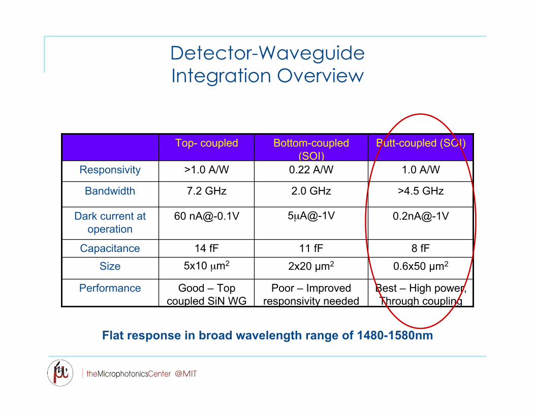
Detector-WaveguideIntegration Overview
0.6x50 µm22x20 µm25x10 µm2Size
Best – High power,Through coupling
Poor – Improvedresponsivity needed
Good – Topcoupled SiN WG
Performance
8 fF11 fF14 fFCapacitance
0.2nA@-1V5µA@-1V60 [email protected] current atoperation
>4.5 GHz2.0 GHz7.2 GHzBandwidth
1.0 A/W0.22 A/W>1.0 A/WResponsivity
Butt-coupled (SOI)Bottom-coupled(SOI)
Top- coupled
Flat response in broad wavelength range of 1480-1580nm
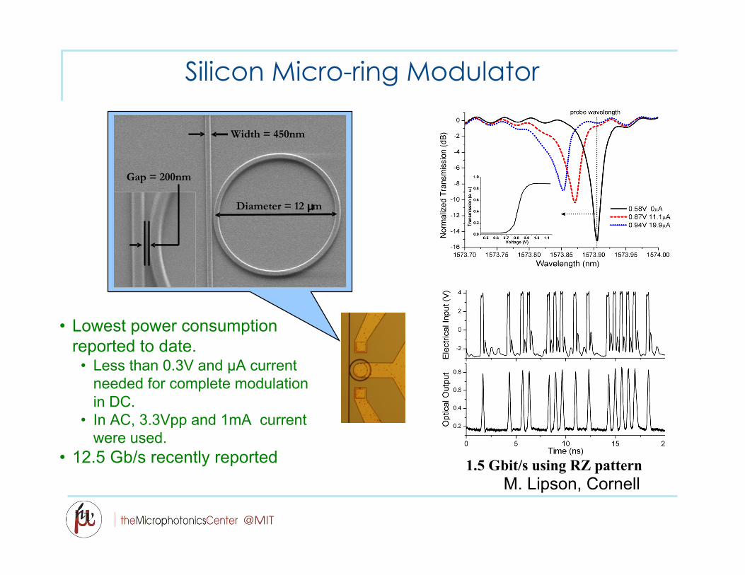
Silicon Micro-ring Modulator
1.5 Gbit/s using RZ pattern
• Lowest power consumptionreported to date.• Less than 0.3V and µA current
needed for complete modulationin DC.
• In AC, 3.3Vpp and 1mA currentwere used.
• 12.5 Gb/s recently reported
Diameter = 12 μm
Width = 450nm
Gap = 200nm
M. Lipson, Cornell
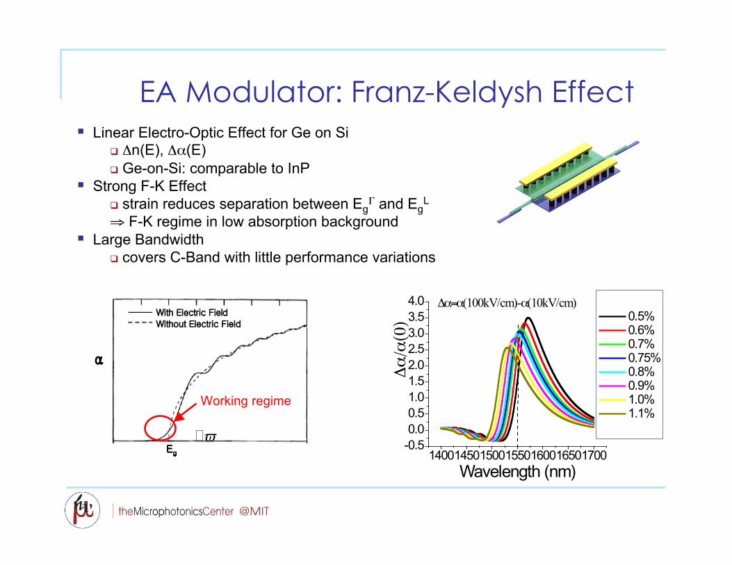
EA Modulator: Franz-Keldysh Effect
1400145015001550160016501700-0.5
0.0
0.5
1.0
1.5
2.0
2.5
3.0
3.5
4.0 !"="(100kV/cm)-"(10kV/cm)
!"/"(0)
Wavelength (nm)
0.5% 0.6% 0.7% 0.75% 0.8% 0.9% 1.0% 1.1%
Linear Electro-Optic Effect for Ge on Si Δn(E), Δα(E) Ge-on-Si: comparable to InP
Strong F-K Effect strain reduces separation between Eg
Γ and EgL
⇒ F-K regime in low absorption background Large Bandwidth
covers C-Band with little performance variations
Eg
With Electric Field
Without Electric Field
α
ϖ�Eg
With Electric Field
Without Electric Field
α
ϖ�
Working regime
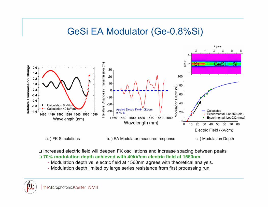
GeSi EA Modulator (Ge-0.8%Si)
Increased electric field will deepen FK oscillations and increase spacing between peaks 70% modulation depth achieved with 40kV/cm electric field at 1560nm
- Modulation depth vs. electric field at 1560nm agrees with theoretical analysis.- Modulation depth limited by large series resistance from first processing run
1460 1480 1500 1520 1540 1560 1580-1.0
-0.8
-0.6
-0.4
-0.2
0.0
0.2
0.4
0.6
Rel
ativ
e Tr
ansm
issi
on C
hang
e
Wavelength (nm)
Calculation 8 kV/cm Calculation 40 kV/cm
0 10 20 30 40 50 60 70 800
20
40
60
80
100
Experimental, Lot 032 (new) Experimental, Lot 350 (old)
Mod
ulat
ion
Dep
th (%
)
Electric Field (kV/cm)
Calculated
a. ) FK Simulations b. ) EA Modulator measured response c. ) Modulation Depth
Si SiGeSi
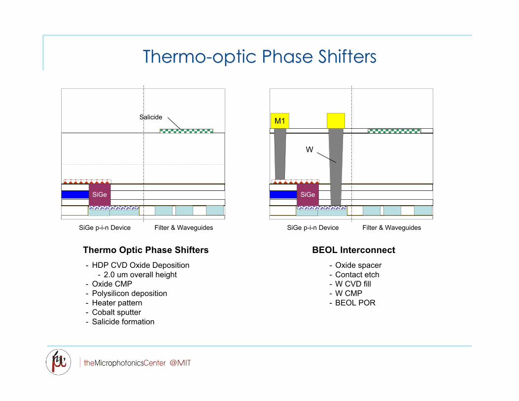
Thermo-optic Phase ShiftersThermo-optic Phase Shifters
Thermo Optic Phase Shifters- HDP CVD Oxide Deposition
- 2.0 um overall height- Oxide CMP- Polysilicon deposition- Heater pattern- Cobalt sputter- Salicide formation
SiGe
SiGe p-i-n Device Filter & Waveguides
BEOL Interconnect
SiGe
M1
SiGe p-i-n Device Filter & Waveguides
- Oxide spacer- Contact etch- W CVD fill- W CMP- BEOL POR
Salicide
W
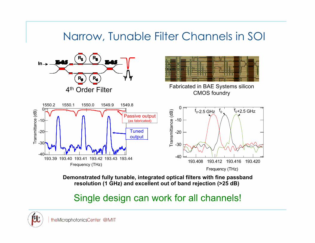
Narrow, Tunable Filter Channels in SOI
Single design can work for all channels!
-40
-30
-20
-10
0
Tra
nsm
itta
nce
(d
B)
193.420193.416193.412193.408
Frequency (THz)
f0
f0+2.5 GHzf0-2.5 GHz
Fabricated in BAE Systems siliconCMOS foundry
Demonstrated fully tunable, integrated optical filters with fine passbandresolution (1 GHz) and excellent out of band rejection (>25 dB)
In !=0.5R1 R2
R3 R4
!=0.5In !=0.5R1 R2
R3 R4
!=0.5
-40
-30
-20
-10
0
Tra
nsm
itta
nce
(d
B)
193.44193.43193.42193.41193.40193.39
Frequency (THz)
1550.2 1550.1 1550.0 1549.9 1549.8
Tuned
output
Tuned
output
Tuned
output
Tuned
output
Passive output(as fabricated)
Passive output(as fabricated)
4th Order Filter
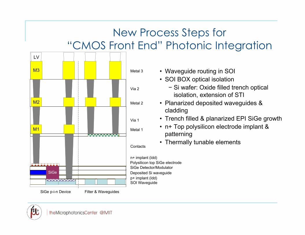
New Process Steps for“CMOS Front End” Photonic Integration
SiGe
M1
M2
M3
Deposited Si waveguide
LV
Via 2
Via 1
Contacts
SOI Waveguide
• Waveguide routing in SOI• SOI BOX optical isolation− Si wafer: Oxide filled trench optical
isolation, extension of STI• Planarized deposited waveguides &
cladding• Trench filled & planarized EPI SiGe growth• n+ Top polysilicon electrode implant &
patterning• Thermally tunable elements
Polysilicon top SiGe electrodeSiGe Detector/Modulator
Metal 1
Metal 2
Metal 3
p+ implant (ldd)
n+ implant (ldd)
SiGe p-i-n Device Filter & Waveguides
Outline
Si CMOS Platform
Photonic Materials- Silicon
- Germanium
Active photonic devices- Detectors
- Modulators
Chipscale Photonic Networks
Summary
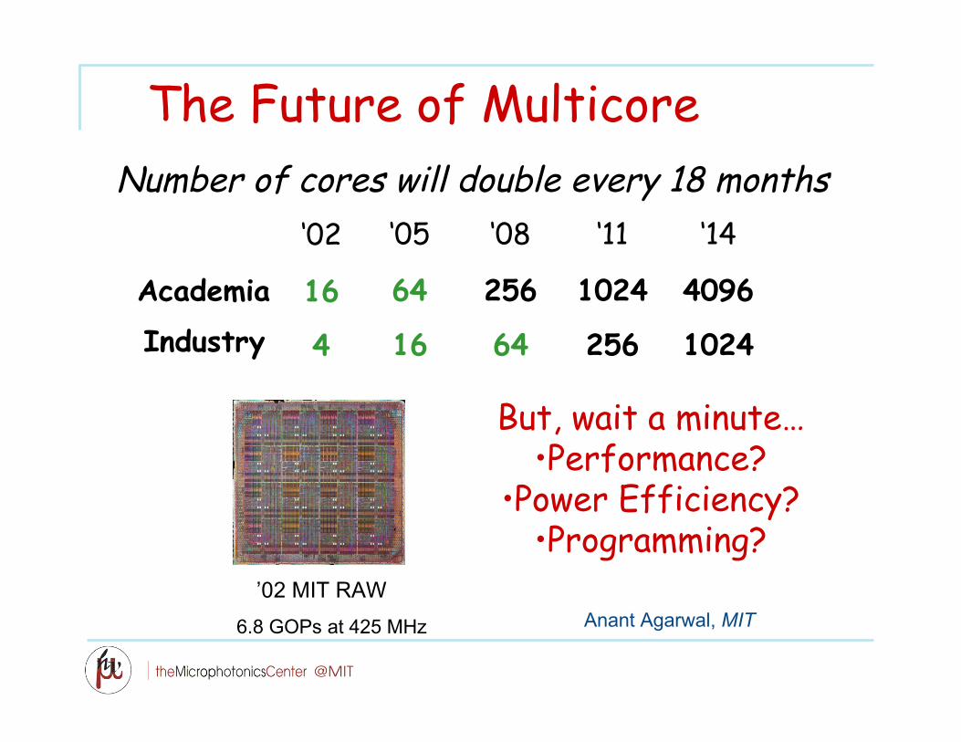
The Future of MulticoreNumber of cores will double every 18 months
‘05 ‘08 ‘11 ‘14
64 256 1024 4096
‘02
16AcademiaIndustry 16 64 256 10244
But, wait a minute…•Performance?
•Power Efficiency?•Programming?
Anant Agarwal, MIT’02 MIT RAW
6.8 GOPs at 425 MHz
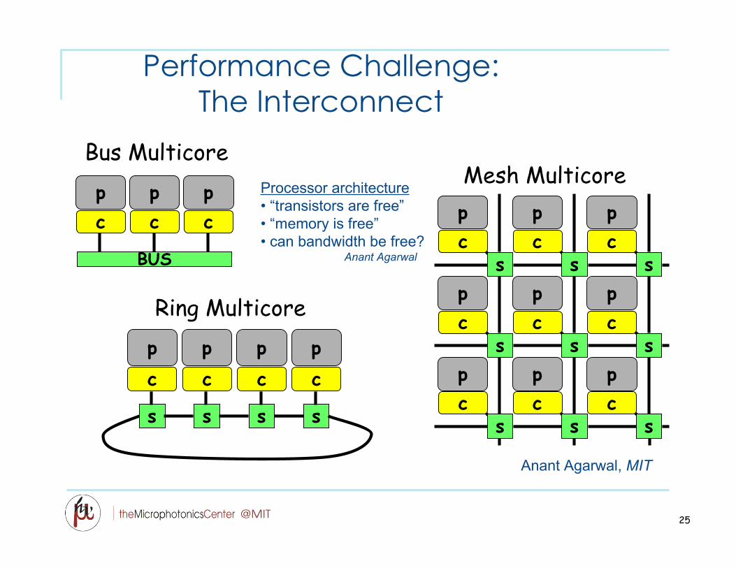
Performance Challenge:The Interconnect
BUS
pc
pc
pc
Bus Multicore
s s s s
pc
pc
pc
pc
Ring Multicore
pc
s
pc
s
pc
s
pc
s
pc
s
pc
s
pc
s
pc
s
pc
s
Mesh Multicore
25
Anant Agarwal, MIT
Processor architecture• “transistors are free”• “memory is free”• can bandwidth be free? Anant Agarwal
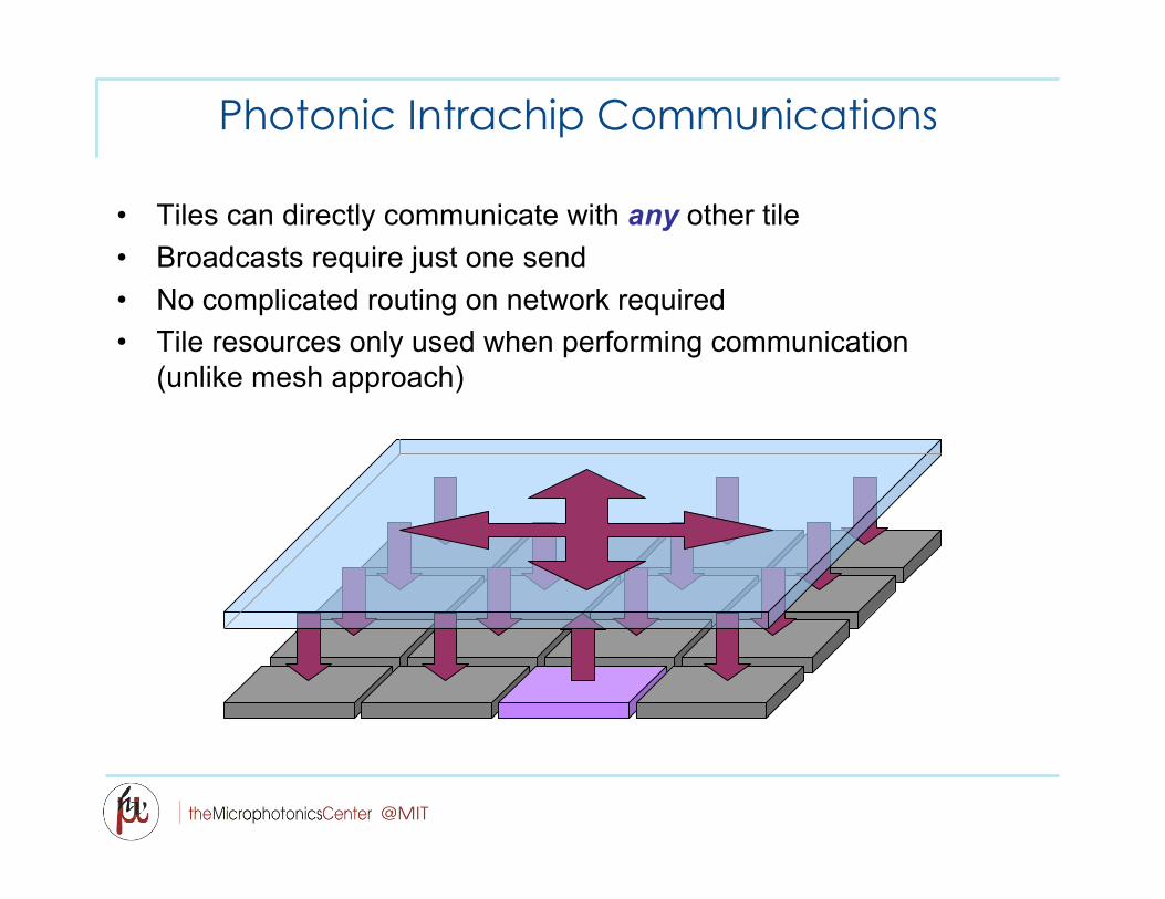
Photonic Intrachip Communications
• Tiles can directly communicate with any other tile• Broadcasts require just one send• No complicated routing on network required• Tile resources only used when performing communication
(unlike mesh approach)
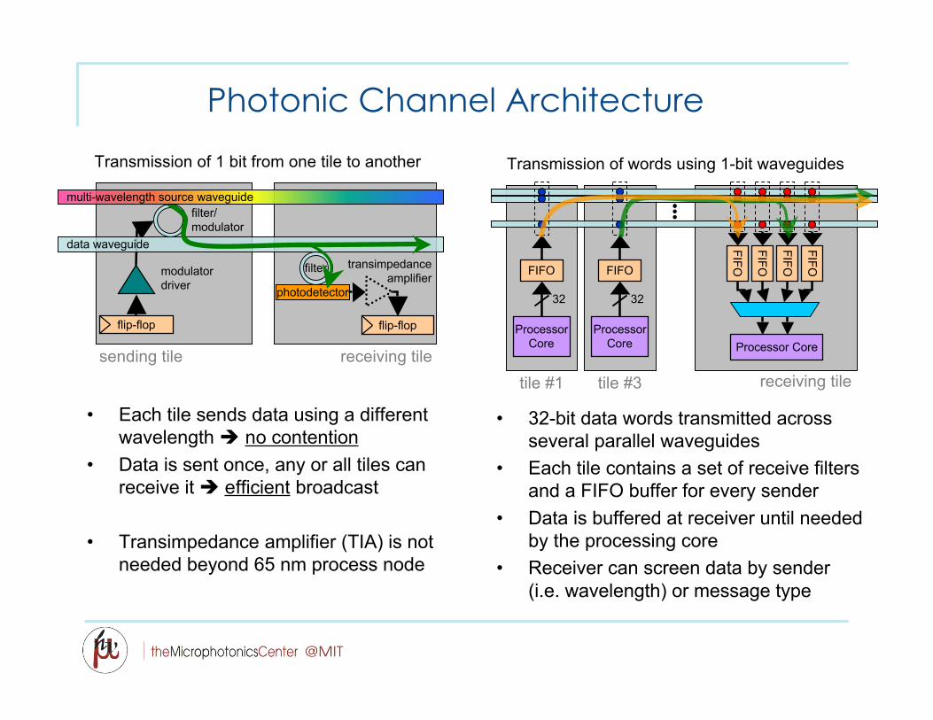
Photonic Channel Architecture
tile #1 receiving tile
Transmission of words using 1-bit waveguides
tile #3
FIFO
32
ProcessorCore
FIFO
sending tile receiving tile
flip-flop flip-flop
filter
photodetector
filter/modulator
modulatordriver
data waveguide
transimpedanceamplifier
multi-wavelength source waveguide
Transmission of 1 bit from one tile to another
FIFO
32
ProcessorCore
FIFO
FIFO
FIFO
Processor Core
• 32-bit data words transmitted acrossseveral parallel waveguides
• Each tile contains a set of receive filtersand a FIFO buffer for every sender
• Data is buffered at receiver until neededby the processing core
• Receiver can screen data by sender(i.e. wavelength) or message type
• Each tile sends data using a differentwavelength no contention
• Data is sent once, any or all tiles canreceive it efficient broadcast
• Transimpedance amplifier (TIA) is notneeded beyond 65 nm process node
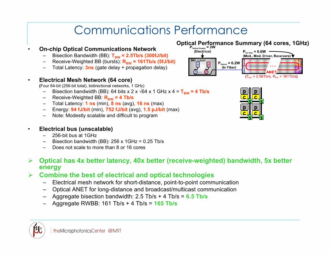
Communications Performance• On-chip Optical Communications Network
– Bisection Bandwidth (BB): TBW = 2.5Tb/s (300fJ/bit)– Receive-Weighted BB (bursts): RBW = 161Tb/s (5fJ/bit)– Total Latency: 3ns (gate delay + propagation delay)
• Electrical Mesh Network (64 core)(Four 64-bit (256-bit total), bidirectional networks, 1 GHz)
– Bisection bandwidth (BB): 64 bits x 2 x √64 x 1 GHz x 4 = TBW = 4 Tb/s– Receive-Weighted BB: RBW = 4 Tb/s– Total Latency: 1 ns (min), 8 ns (avg), 16 ns (max)– Energy: 94 fJ/bit (min), 752 fJ/bit (avg), 1.5 pJ/bit (max)– Note: Modestly scalable and difficult to program
• Electrical bus (unscalable)– 256-bit bus at 1GHz– Bisection bandwidth (BB): 256 x 1GHz = 0.25 Tb/s– Does not scale to more than 8 or 16 cores
Optical has 4x better latency, 40x better (receive-weighted) bandwidth, 5x betterenergy
Combine the best of electrical and optical technologies– Electrical mesh network for short-distance, point-to-point communication– Optical ANET for long-distance and broadcast/multicast communication– Aggregate bisection bandwidth: 2.5 Tb/s + 4 Tb/s = 6.5 Tb/s– Aggregate RWBB: 161 Tb/s + 4 Tb/s = 165 Tb/s
Optical Performance Summary (64 cores, 1GHz)
pcs
pc
s
pcs
pc
s
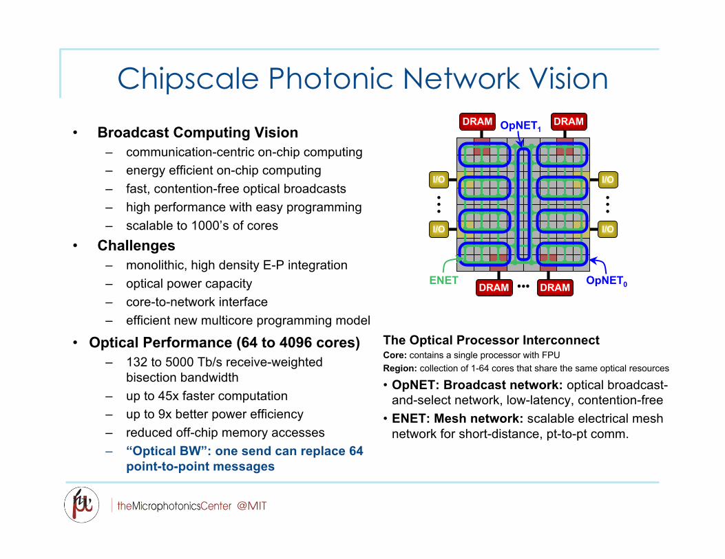
Chipscale Photonic Network Vision
The Optical Processor InterconnectCore: contains a single processor with FPURegion: collection of 1-64 cores that share the same optical resources
• OpNET: Broadcast network: optical broadcast-and-select network, low-latency, contention-free
• ENET: Mesh network: scalable electrical meshnetwork for short-distance, pt-to-pt comm.
• Broadcast Computing Vision– communication-centric on-chip computing– energy efficient on-chip computing– fast, contention-free optical broadcasts– high performance with easy programming– scalable to 1000’s of cores
• Challenges– monolithic, high density E-P integration– optical power capacity– core-to-network interface– efficient new multicore programming model
• Optical Performance (64 to 4096 cores)– 132 to 5000 Tb/s receive-weighted
bisection bandwidth– up to 45x faster computation– up to 9x better power efficiency– reduced off-chip memory accesses– “Optical BW”: one send can replace 64
point-to-point messages
DRAMDRAM
DRAMDRAM
I/O
ENET OpNET0
OpNET1
I/O I/O
I/O
Conquering the Last Centimeter
• Integration creates a circuit function.– not customized perfect devices
• A microphotonic circuit contains replicated circuitelements on a standard platform.– materials, processes, design and fab tools
Has potential to provide the majority of low-costphotonic interconnects in the medium to long term
Silicon Microphotonics is the only option for continuedexponential increase in chip performance.
The Philosophy

Thank You


![Monolithic silicon-photonic platforms in state-of-the-art ... · Monolithic silicon-photonic platforms in state-of-the-art CMOS SOI processes [Invited] VLADIMIR STOJANOVIC´,1,2,*](https://img.pdfslide.us/doc/110x75/60a637b0c73a7d69b73b52dd/monolithic-silicon-photonic-platforms-in-state-of-the-art-monolithic-silicon-photonic.jpg)