Embed Size (px)
Citation preview

This content has been downloaded from IOPscience. Please scroll down to see the full text.
Download details:
IP Address: 134.79.222.200
This content was downloaded on 22/10/2013 at 16:50
Please note that terms and conditions apply.
Momentum-resolved electronic structure at a buried interface from soft X-ray standing-wave
angle-resolved photoemission
View the table of contents for this issue, or go to the journal homepage for more
2013 EPL 104 17004
(http://iopscience.iop.org/0295-5075/104/1/17004)
Home Search Collections Journals About Contact us My IOPscience

October 2013
EPL, 104 (2013) 17004 www.epljournal.org
doi: 10.1209/0295-5075/104/17004
Momentum-resolved electronic structure at a buried interfacefrom soft X-ray standing-wave angle-resolved photoemission
A. X. Gray1, 2, 3
, J. Minar4, L. Plucinski
5, M. Huijben
6, A. Bostwick
7, E. Rotenberg
7, S.-H. Yang
8,
J. Braun4, A. Winkelmann
9, G. Conti
1,2, D. Eiteneer
1,2, A. Rattanachata
1,2, A. A. Greer
1,2,
J. Ciston10
, C. Ophus10
, G. Rijnders6, D. H. A. Blank
6, D. Doennig
11, R. Pentcheva
11, J. B. Kortright
2,
C. M. Schneider5, H. Ebert
4 and C. S. Fadley1,2
1 Department of Physics, University of California Davis - Davis, CA 95616, USA2 Materials Sciences Division, Lawrence Berkeley National Laboratory - Berkeley, CA 94720, USA3 Stanford Institute for Materials and Energy Science, Stanford University and SLAC National Accelerator Laboratory2575 Sand Hill Road, Menlo Park, CA 94029, USA4 Department of Chemistry, Physical Chemistry Institute, Ludwig-Maximilians University-Munich - Munich,Germany5 Peter-Grunberg-Institut PGI-6, Forschungszentrum Julich GmbH - 52425 Julich, Germany6 Faculty of Science and Technology, MESA+ Institute for Nanotechnology, University of Twente - Enschede,The Netherlands7 Advanced Light Source, Lawrence Berkeley National Laboratory - Berkeley, CA 94720, USA8 IBM Almaden Research Center - San Jose, CA 95120, USA9 Max-Planck-Institut fur Mikrostrukturphysik - Weinberg 2, D-06120 Halle (Saale), Germany10 National Center for Electron Microscopy, Lawrence Berkeley National Laboratory - Berkeley, CA 94720, USA11 Department of Earth and Environmental Sciences and Center of Nanoscience (CENS),Ludwig-Maximilians University-Munich - Munich, Germany
received on 12 September 2013; accepted by J. Fink on 4 October 2013published online 22 October 2013
PACS 79.60.Jv – Interfaces; heterostructures; nanostructuresPACS 68.49.Uv – X-ray standing wavesPACS 85.75.Dd – Magnetic memory using magnetic tunnel junctions
Abstract – Angle-resolved photoemission spectroscopy (ARPES) is a powerful technique for thestudy of electronic structure, but it lacks a direct ability to study buried interfaces between two ma-terials. We address this limitation by combining ARPES with soft X-ray standing-wave (SW) exci-tation (SWARPES), in which the SW profile is scanned through the depth of the sample. We havestudied the buried interface in a prototypical magnetic tunnel junction La0.7Sr0.3MnO3/SrTiO3.Depth- and momentum-resolved maps of Mn 3d eg and t2g states from the central, bulk-likeand interface-like regions of La0.7Sr0.3MnO3 exhibit distinctly different behavior consistent witha change in the Mn bonding at the interface. We compare the experimental results to state-of-the-art density-functional and one-step photoemission theory, with encouraging agreement thatsuggests wide future applications of this technique.
Copyright c© EPLA, 2013
Introduction. – Angle-resolved photoemission(ARPES) is the technique of choice for probing the elec-tronic structure of solids and surfaces, yielding as directoutput a map of photoelectron intensities as a function ofthe electron kinetic energy Ekin and electron momentum�p = h�k, and it has been applied to virtually every typeof crystalline, or even quasicrystalline material [1,2]. Atypical experimental setup involving a hemisphericalelectrostatic analyzer is shown in fig. 1(a). For excitation
with a photon energy hν, three-dimensional datasets ofkinetic energy Ekin(�k) or binding energy relative to theFermi level EF
b (�k) ≈ hν − Ekin(�k) as a function of the kx
and ky components are obtained by measuring detectorimages of Ekin vs. the take-off angle θTOA and scanningalso the orthogonal angle βTOA by rotating the sample.Each point in this volume can in turn be mapped into thereduced Brillouin zone (BZ) via direct transitions (DTs)that in their simplest form obey the conservation law
17004-p1

A. X. Gray et al.
Fig. 1: (Color online) Experimental setup and basic principles of standing-wave (SW) ARPES (SWARPES). (a) Schematicdiagram of the ARPES experiment illustrating the angular degrees of freedom for the sample manipulation (θTOA and βTOA),the hemispherical electrostatic photoelectron analyzer, the position-sensitive multichannel plate (MCP) detector with twoorthogonal axes x = kx and y = Ekin, and the final CCD screen with the resulting Ekin vs. kx dispersion. The angle betweenphoton incidence and the spectrometer lens axis was 60◦, with both directions lying in the x-z plane. (b) Schematic diagramof the investigated multilayer structure consisting of 120 bilayers of STO and LSMO grown epitaxially on a single-crystalSTO substrate, with each bilayer consisting of 4 units cells (15.61 A) of STO and 4 unit cells (15.51 A) of LSMO. A photonenergy of 833.2 eV corresponding to the maximum reflectivity at the La 3d5/2 absorption edge was used for the photoemission
experiments [17]. An example of the Ekin(�k) distribution for a fixed value of the binding energy EB is shown above the sample.(c) SW-excited photoemission intensity rocking curves (RCs) for Ti 2p3/2 and Mn 3p core-levels (solid curves), as well as theX-ray optical simulations fitted to them (dashed curves), and previously yielding the chemical depth profile of the sample [17].(d) Simulated intensity of the X-ray SW electric field (E2) inside the sample as a function of the depth and grazing incidenceangle. The line-cuts indicate that, for incidence angles <12.4◦, the SW field highlights the bulk or center of the LSMO layer,but for angles >12.9◦ the interface regions of the LSMO layer are emphasized.
�k = �ki + �ghk� + �khν , where �ki is in the reduced BZ, �ghk�
is a bulk reciprocal lattice vector, and �khν is the photonwave vector, which must be considered for energies in thesoft and hard X-ray regimes above about 0.5 keV due tonon-dipole effects [3,4].
However, a significant disadvantage of the conventionalARPES technique is its extreme surface sensitivity, dueto the very low inelastic mean-free paths (IMFPs) ofthe electrons photoemitted using radiation in the range25 eV < hv < 150 eV [5]. As a quantitative example, theIMFP, which is in turn the average depth in normal emis-sion, for the complex oxides SrTiO3 or La0.7Sr0.3MnO3
of interest here can be estimated to be about 1.9 A athv = 25 eV, and 5.9 A at hv = 150 eV [5,6], or only a cou-ple of atomic layers below the surface. A recent ARPESstudy of La0.7Sr0.3MnO3 illustrates this surface sensitiv-ity [7]. This has led in recent years to more bulk-sensitiveARPES measurements at higher photon energies and thuslarger IMFPs in the 10–100 A range that are by now be-ing carried out in the soft X-ray regime of 500–1200 eV forvarious materials [3,4,8–11], as well as in the hard X-rayregime from 3.2 to 5.9 keV [12,13].
Yet, even at these higher photon energies, the photoe-mission signal originating closer to the surface will bestronger than the signal originating from below accord-ing to I(z) = I0 exp[−z/Λ sin θTOA], where z is the depth,Λ is the IMFP, or more correctly the effective attenua-tion length (EAL) that includes elastic scattering effectsas well [5] and θTOA is the electron take-off angle relativeto the surface (cf. fig. 1(a)) [5,6]. Controllable depth selec-tivity can however be accomplished by setting up an X-ray
standing-wave (SW) field in the sample by growing it as,or on, a synthetic periodic multilayer mirror substrate,which in first-order Bragg reflection acts as a strong SWgenerator [14,15]. The maxima of the SW can be movedin the z-direction perpendicular to the sample surface byscanning the incidence angle θinc through the Bragg condi-tion, thus generating a well-known rocking curve (RC) ofintensity [14–16]. Angle-integrated SW-excited X-ray pho-toemission (SW-XPS) from core-levels and valence bandshas been applied previously in studies of various systems,in particular layers and interfaces of relevance to giantmagnetoresistance (GMR) and tunnel magnetoresistance(TMR) [16], including the insulator/half-metallic fer-romagnet system SrTiO3/La0.7Sr0.3MnO3 (STO/LSMO)that is the topic of this study [17], but �k-resolved ARPEShas not previously been attempted. These prior SW-XPS studies were carried out at room temperature, suchthat phonon-induced non-direct transitions (NDTs) led toan averaging over the BZ, and resultant valence spectrathat closely resemble matrix-element weighted densitiesof states (MEW-DOS) [3,4]. It is possible to estimate thefraction of DTs from a photoemission Debye-Waller factorof the form W (T ) = exp[− 1
3g2hk�〈U2(T )〉], where U2(T ) is
the three-dimensional mean-squared vibrational displace-ment [3,4], and we consider this aspect further below andin our Supplementary Information (SI) [18].
In this letter, we add depth selectivity to ARPES bycombining more bulk-sensitive soft X-ray excitation atca. 800 eV corresponding to IMFPs of about 19 A with theSW approach (SWARPES) to provide a unique depth- and�k-resolved probe of buried layer and interface electronic
17004-p2
Momentum-resolved electronic structure at a buried interface from SWARPES
structure. Interface electronic structure is known to becrucial to the properties of various nanoscale multilayersystems, as for example, in the magnetic tunnel junction(MTJ) Fe/MgO, for which the Δ1 band of Fe is thoughtto be the predominant carrier of spin-polarized tunnelingcurrent [19,20], and the interface between STO and LAOin the system LaAlO3/SrTiO3, for which the interface pro-vides a 2D electron gas that has been shown to be bothferromagnetic and superconducting [21]. Yet there are upto now no techniques for directly studying the interfaceelectronic structure in a �k-resolved manner. We illustratethe capability of SWARPES to do this for a prototypi-cal oxide MTJ, La0.7Sr0.3MnO3/SrTiO3 (LSMO/STO) bycomparing experiment to theory of several types, includ-ing, in particular, state-of-the-art one-step photoemissioncalculations.
The much-studied LSMO/STO system is a promisingcandidate for a MTJ [22–24], wherein the half-metallic na-ture of ferromagnetic LSMO is responsible for producinga 100% spin-polarized tunneling current across the STOinsulating barrier [25,26]. Up to now, however, the theo-retically predicted TMR effect of 100% [27] has not beenrealized, with the highest TMR values reported so far be-ing on the order of 80% [28–30]. The most widely acceptedexplanation for this reduced performance is highly local-ized interface effects in the LSMO layer near the inter-face with STO [31]. In a prior angle-integrated SW-XPSstudy of LSMO/STO [17], we have investigated the chem-ical and electronic structure profiles of the LSMO/STOinterface via core-level soft and hard X-ray SW-excitedphotoemission, X-ray absorption and X-ray reflectivity, inconjunction with X-ray optical [32] and core-hole multiplettheoretical modeling [33,34] Analysis of the core-level SWmodulations revealed the presence of an interdiffusion re-gion of 4–5 A in thickness (a little over 1 unit cell) betweenthe STO and LSMO layers, a change in the soft X-ray op-tical coefficients of LSMO near the interface, and a shiftin the position of the Mn 3p peak near the interface thatis consistent with a crystal-field distortion effect. What isstill needed however is depth- and �k-resolved informationconcerning the valence electronic states. We show herethat SWARPES can provide this.
The LSMO/STO multilayer sample consisted of 120 bi-layers, each consisting of 4 unit cells of LSMO (∼15.51 A)and 4 unit cells of STO (∼15.61 A), with STO terminat-ing the structure, as shown schematically in fig. 1(b), andwas fabricated using the pulsed laser deposition (PLD)technique (see details in the SI [18]). The transport andmagnetic properties of the LSMO/STO superlattice areconsistent with previous reports [35], as shown in ourSI [18].
The SWARPES measurements were carried out atthe Electronic Structure Factory (ESF) endstation atBeamline 7.0.1 of the Advanced Light Source (LawrenceBerkeley National Laboratory) using a Scienta R4000spectrometer. The measurements were performed at atemperature of 20K and with an overall energy resolution
of ∼300meV, with some reference data taken at 300K. Inorder to maximize reflectivity and thus also the contrast ofthe SW, and therefore to better define the depth-resolvedphotoemission within the sample, the excitation energywas set to 833.2 eV, which is just below the La 3d5/2
absorption edge, as discussed elsewhere [17].In order to verify the presence of the SW in the su-
perlattice, and to most quantitatively model the intensityprofile of it within the sample, we first performed core-levelSW-XPS measurements. Strong SW RC intensity modu-lations near the Bragg condition for the superlattice wereobserved for Ti 2p3/2 and Mn 3p core-levels (solid curvesin fig. 1(c); these are fully consistent with our prior studyof a similar LSMO/STO sample [17]. These RCs werefitted using a specially written theoretical code [32] in or-der to confirm the chemical profile of the structure withangstrom level accuracy, and the best-fit theoretical curvesare shown as dashed curves in fig. 1(c). The conclusions ofthis SW-XPS analysis were also verified by sub-angstromscanning transmission electron microscopy (STEM) andelectron energy loss spectroscopy (EELS), as discussed inour SI [18]. The same X-ray optical model and sampleconfiguration were then used to simulate the electric-fieldintensity (E2) profile of the SW inside the superlatticeas a function of depth and incidence angle. The resultsof these simulations in fig. 1(d) reveal that the SW max-ima will highlight the center (“bulk”) region of the buriedLSMO layer at an incidence angle of 12.4◦ (a maximum ofMn 3p intensity), as shown in the left line-cut. Increasingthe incidence angle past the Bragg condition, we shift theSW downwards by about half-a-period, highlighting theinterfacial region of the LSMO layer at angles above 12.9◦
(a maximum of Ti 2p intensity), as shown in the rightline-cut.
Three-dimensional SWARPES measurements were thusperformed at these two incidence angles, as well as others,finally yielding EF
B (kx, ky(kz)), with kz implicitly knownbut not directly measured. To validate our final conclu-sions, we have also measured SWARPES at an additionalfive angles to the left (11.82◦, 12.10◦) and right (13.35◦,13.90◦) of the RC, as well as in the middle of it (12.15◦);some of these results at other angles are presented in ourSI [18]. As noted in prior higher-energy ARPES stud-ies [11–13], it is useful to correct such data for the effectsof phonon-induced MEW-DOS–like background intensity,as well as X-ray photoelectron diffraction (XPD) effects,which in our SWARPES data can be estimated from therelevant Debye-Waller factors to represent ca. 25% of theintensity. Correction for DOS and XPD effects can to firstorder be done by dividing the data successively by theaverage over angle and the average over energy of eachdetector image, respectively [36] as demonstrated for ex-perimental data from W and GaAs recently [12,13]. Herewe have also taken the XPD correction one step further bymeasuring the Mn 3p core-level, as discussed in detail inour SI [18]: however, none of our final conclusions dependson this additional correction.
17004-p3

A. X. Gray et al.
In fig. 2, we now show some key SWARPES resultsfor five key binding-energy positions, all corrected inthe same two-step way to remove any DOS or XPD ef-fects. Figure 2(a) shows a reference, angle-integrated spec-trum spanning the Fermi-referenced binding-energy win-dow from +1 eV to −9 eV, including five major featureslabeled 1–5; this curve, obtained at room temperature,should roughly represent the MEW-DOS for the sam-ple. The region between the binding energies of 0 eV and−3.25 eV contains the LSMO-derived states, specificallyMn 3d eg (feature 1, at ca. 1.0 eV) and Mn 3d t2g (fea-ture 2, at ca. 2.4 eV), and no STO-derived states due tothe bandgap “window” [18,37]. Conversely, the region be-tween −3.25 eV and −7.0 eV we expect to be dominated bythe states originating in the topmost STO layer (labeled3, 4, and expected to be relatively flat complex bands).The deeper bands from LSMO will also show up in this re-gion, but with attenuated intensity due to the STO layer.However, we finally suggest that feature 5 is predomi-nantly LSMO-derived, and show evidence below and inour SI [18] for this interpretation. Figures 2(b), (c) and (d)now show the corrected low-temperature ARPES intensitymaps in (kx, ky) summed over 300meV intervals centeredat binding energies 1–5 for the bulk-LSMO–sensitive in-cidence angle (b), the interface-sensitive angle (c), andthe bulk-minus-interface difference between the two (d).The contrast of the color map in the difference map offig. 2(d) is enhanced in order to accentuate the smaller dif-ferences between the bulk-like and interface-like features.Note the indication of the surface normal and the firstBrillouin zone in the image in fig. 2(b). Multiple Bril-louin zones are thus represented in these images due tothe large k vector of a photoelectron at 833.2 eV excita-tion energy (14.8 A
−1, compared to the BZ dimensions in
STO or LSMO of 2π/a ≈ 1.61 A−1
), and the fact that thecombined detector image and βTOA scan span 35◦ in kx
and 40◦ in ky.
The bulk- and interface-sensitive maps at a given energyare at first sight very similar, although those for differentenergies clearly differ markedly from one another. Themost dispersive features 1, 2, and 5 show the most struc-ture, and the less dispersive STO bands 3 and 4 showmuch less structure. Feature 5 is striking in showing a re-markably simple square pattern that essentially representsthe expected BZ repeat pattern; this simple appearanceadditionally confirms the validity of our DOS and XPDcorrection procedures. The bulk-minus-interface maps arefinally crucial indicators of changes in the electronic struc-ture at the interface. The biggest changes (up to ∼4.5%in intensity) are observed for the LSMO-derived Mn 3deg and t2g electronic states at energies 1 and 2, suggest-ing significant changes in the (kx, ky) dependence of thesestates at the LSMO/STO interface, including a generalsuppression of intensity. The STO-dominated states atthe binding energies of 4.0 and 6.2 eV show less momen-tum dispersion in general, and thus also exhibit only minor
Fig. 2: (Color online) Depth-resolved SWARPES measure-ments of the LSMO/STO superlattice. (a) An angle-integratedspectrum spanning a binding-energy window of 10 eV (from+1 eV to −9 eV), and including all the major features of thevalence bands, labeled 1–5, with their origins and charactersindicated. (b) SWARPES data for these five energies in a bulk-LSMO-sensitive SW measurement geometry. Binding-energyintegration windows of 300 meV (consistent with our total en-ergy resolution) centered around the binding energies of the fivefeatures discernible in the angle-integrated valence spectra (asdetermined by peak-fitting), were used to obtain these plots.Shown are XPD-normalized angle-resolved (kx, ky) photoemis-sion intensity maps of the Mn 3d eg (1), Mn 3d t2g (2) states,the largely STO-derived states (3 and 4), and the valence bandbottom states (5) due largely to LSMO. (c) As (b), but foran LSMO/STO-interface–sensitive measurement geometry ofthe SW. (d) Bulk-interface difference (kx, ky) maps based on(b) and (c), revealing the most significant differences for theLSMO-derived Mn 3d eg and Mn 3d t2g states at the interfacebetween STO and LSMO, and as well as the dispersive valenceband bottom bands 5 from LSMO. The intensity scales at rightindicate the relative amplitudes of the effects.
bulk-interface changes. Finally, the local-density theoryshown in our SI [18] indicates that the largely LSMO-derived states 5 at ∼7.5 eV also exhibit a marked changein the (kx, ky) dependence near the interface. All of thesechanges, although subtle, represent a unique experimentalinsight into the interface electronic structure, and we haveverified the validity of these bulk-surface difference effectsby making similar difference maps for points on either sideof the RC, which are found to show no discernible effects(see our SI [18]).
In comparing our experimental results to theory, we willconsider only k-space maps for the LSMO-derived features1 and 2 representing Mn 3d t2g and eg states, and feature5 at the bottom of the valence bands that exhibits a verysimple dispersion pattern. Figure 3(a) first presents theresults of simple free-electron final-state calculations in-volving direct transitions from LSMO band-structure cal-culations performed using the Wien2k code at the localdensity approximation + U (LDA + U) level to allow for
17004-p4

Momentum-resolved electronic structure at a buried interface from SWARPES
Fig. 3: (Color online) Theoretical calculations for SWARPESfrom levels Mn 3d eg (1), Mn 3d t2g (2) and the bottom of thevalence bands (5). (a) Simple free-electron final-state theorywith direct transitions from an LDA+U-based band structure(see our SI [18]). Yellow corresponds to spin-up (majority)bands, and red to spin-down (minority). (b), (c), and (d)More accurate one-step photoemission theory summing overboth spin polarizations and with the SW intensity profile in-cluded, for a bulk-LSMO–sensitive geometry (b), an interface-sensitive geometry (c), and the bulk-minus-interface difference(d), respectively. The amplitudes of the effects are again in-dicated. (e) represents a direct comparison to experimentalpanels from fig. 2(d).
correlation effects [38]. Here the LSMO is assumed to beferromagnetic and the spin of the photoelectrons is dis-tinguished by color (red = majority, yellow = minority);thus the eg allowed transitions are all majority or red. Theagreement between the experiment and theory is very en-couraging for all three energies, with the BZ periodicityand positions of some of the major features reproducedwell, although of course there is no information in thesek-space maps as to relative photoemission intensities, sinceno allowance is made for matrix elements. Analyzing fea-ture 5 with the LSMO band structure is also found to bevalid from LDA calculations for the full multilayer, whichpredict that the valence band minimum of LSMO is belowthat of STO (see our SI [18]).
In figs. 3(b)–(d) we present the results of a muchmore accurate one-step photoemission theory basedon a fully relativistic LDA+U layer-KKR (Korringa-Kohn-Rostoker) approach and a time-reversed LEED
(low-energy electron diffraction) final state [39] (furtherdetails in our SI [18]), as applied to the actual multilayerstructure with the explicitly included surface. These cal-culations furthermore incorporate a first attempt to in-clude the intensity profile of the X-ray SW by using asan additional input the |E2| profiles shown in fig. 1(d).The resulting bulk- and interface-sensitive photoemissionintensity k-space maps are shown in figs. 3(b), (c). Fi-nally, differences between the bulk and interface electronicstructure were calculated and these are plotted in fig. 3(d),and compared to experiment in fig. 3(e). It is importantto note that this type of one-step theory calculation rep-resents a much more accurate theoretical counterpart tothis particular experiment as compared to the free-electronfinal-state theory, since in addition to calculating true an-gular distributions of photoemission intensities due to SWexcitation, the influence of the top STO overlayer is alsotaken into account, albeit in a rigid lattice approximationso that phonon effects are not included. Thus, althoughthe periodicity of the BZs and the positions of the majorfeatures are similar to those in fig. 3(a), visible differencesare observed between the k-space maps generated usingthese two theoretical approaches.
Comparing the results of the one-step theory calcula-tions to the experimental k-space maps we observe en-couraging similarities. In particular, the sizes of the BZfeatures, and the general intensity variations across theimage, with noticeable depression in intensities in the firstBZ (including eg intensity loss in fig. 2(b), (c)), are wellreproduced. Most importantly, the bulk-interface differ-ence maps for the LSMO-derived Mn 3d eg and t2g statesshow a similar degree of suppression in intensities at theLSMO/STO interface —about 9.5% in theory comparedto 4.5% in experiment. Thus, although we cannot yetclaim a fully quantitative agreement between experimentand theory, these results demonstrate a significant firststep in the interpretation and use of interface-resolvedSWARPES data.
In conclusion, by combining soft X-ray ARPES withSW-excited photoelectron spectroscopy, we have deviseda unique technique for probing the �k-resolved electronicstructure of buried layers and interfaces. By generatingan X-ray SW inside a multilayer sample, and then trans-lating it up and down within the sample by varying theincidence angle, we can selectively probe the electronicstructure emphasizing the bulk of a layer or its interface,and then directly compare the two. We have appliedSWARPES to the investigation of the electronic prop-erties of the buried interface within a magnetic tunneljunction composed of La0.7Sr0.3MnO3/SrTiO3, and dis-covered that the bulk-like and interface-like regions of theburied La0.7Sr0.3MnO3 layer exhibit a distinctly differentbehavior, consistent with a change in the Mn bonding ge-ometry at the La0.7Sr0.3MnO3/SrTiO3 interface observedpreviously [17], but now elaborated with �k resolution. Theexperimental results are further validated via agreement
17004-p5

A. X. Gray et al.
with free-electron final-state model calculations and moreprecise state-of-the-art one-step photoemission theoryincluding matrix-element effects. Future theoretical treat-ments should involve the inclusion of atomic distortionsnear the interface, e.g. incorporating a crystal-field dis-tortion near the interface that is suggested by our priorangle-integrated SW-XPS study of the same system [17]and more detailed calculations presented in our SI [18],as well as a more accurate inclusion of the interface mix-ing/roughness that is also seen in the prior SW-XPS studyof this system [17], as well as TEM+EELS data from thepresent sample [18], the SW intensity profile and phononeffects. We thus suggest that the SWARPES methodshould be of broad use in the future studies of buried lay-ers and interfaces in various types of epitaxial multilayerstructures, including those exhibiting spintronic, ferroelec-tric, multiferroic, and superconducting properties
∗ ∗ ∗
This research was supported by the U.S. Departmentof Energy, Office of Science, Office of Basic Energy Sci-ences, Division of Materials Sciences and Engineering un-der Contract No. DE-AC02-05CH11231, via both theLBNL Materials Sciences Division, Magnetic MaterialsProgram, and the LBNL Advanced Light Source. AXG,DE, and AAG also acknowledge partial salary supportfrom a MURI grant of the Army Research Office (GrantNo. W911-NF-09-1-0398). JM, JB and HE are grate-ful for financial support from the German funding agen-cies DFG (FOR1346 and EB 154/20) and the Germanministry BMBF (05K13WMA). DD and RP acknowledgefunding by the German Science Foundation, SFB/TR80and computational time at the Leibniz Rechenzentrum.Research at Stanford was supported through the Stan-ford Institute for Materials and Energy Science (SIMES)and the LCLS by the US Department of Energy, Office ofBasic Energy Sciences. A portion of this work was per-formed using the TEAM 0.5 microscope at the NationalCenter for Electron Microscopy (NCEM), which is sup-ported by the Office of Science, Office of Basic EnergySciences of the U.S. Department of Energy under Con-tract No. DE-AC02-05CH11231. The authors would alsolike to acknowledge the critical TEM sample preparationwork performed by Marissa Libbee at NCEM.
REFERENCES
[1] Damascelli A., Hussain Z. and Shen Z.-X., Rev. Mod.Phys., 75 (2003) 473.
[2] Lu D. H. et al., Annu. Rev. Condens. Matter Phys., 3(2012) 129.
[3] Plucinski L. et al., Phys. Rev. B, 78 (2008) 035108.[4] Papp C. et al., Phys. Rev. B., 84 (2011) 045433.
[5] Powell C. J. et al., J. Electron Spectrosc. Relat. Phe-nom., 98 (1999) 1.
[6] Tanuma S., Powell C. J. and Penn D. R., Surf. In-terface Anal., 43 (2011) 689.
[7] Krempasky J. et al., J. Electron Spectrosc. Relat. Phe-nom., 181 (2010) 63.
[8] Sekiyama, A. et al., Nature, 403 (2000) 396.[9] Iwasaki T. et al., Phys. Rev. B, 65 (2002) 195109.
[10] Claesson T. et al., Phys. Rev. Lett., 93 (2004) 136402.[11] Fadley C. S., Synchrotron Radiat. News, 25 (2012) 26.[12] Gray A. X. et al., Nat. Mater., 10 (2011) 759.[13] Gray A. X. et al., Nat. Mater., 11 (2012) 957.[14] Yang S.-H. et al., Surf. Sci., 461 (2000) L557.[15] Yang S.-H. et al., J. Phys.: Condens. Matter, 14 (2002)
L407.[16] Yang S.-H. et al., J. Phys.: Condens. Matter, 18 (2006)
L259.[17] Gray A. X. et al., Phys. Rev. B, 82 (2010) 205116.[18] Supplementary Information available online at http://
www.physics.ucdavis.edu/fadleygroup/SWARPES-SI.
pdf.[19] Butler W. H., Zhang X.-G., Schulthess T. C. and
MacLaren J. M., Phys. Rev. B, 63 (2001) 054416.[20] Heiliger C., Zahn P., Yavorsky B. Y. and Mertig
I., Phys. Rev. B, 73 (2006) 214441.[21] Bert J. A., Kalisky B., Bell C., Kim M., Hikita Y.,
Hwang H. Y. and Moler K. M., Nat. Phys., 7 (2011)767.
[22] De Teresa J. M. et al., Phys. Rev. Lett., 82 (1999) 4288.[23] Wolf S. A. et al., Science, 294 (2001) 1488.[24] Tsymbal E. Y., Mryasov O. N. and LeClair P. R.,
J. Phys.: Condens. Matter, 15 (2003) R109.[25] Ma C., Yang Z. and Picozzi S., J. Phys.: Condens.
Matter, 18 (2006) 7717.[26] Chikamatsu A. et al., Phys. Rev. B, 73 (2006) 195105.[27] Park J.-H. et al., Nature, 392 (1998) 794.[28] Yu Lu, Li X. W., Gong G. Q. and Gang Xiao, Phys.
Rev. B, 54 (1996) R8357.[29] Sun J. Z. et al., Appl. Phys. Lett., 69 (1996) 3266.[30] Viret M. et al., Europhys. Lett., 39 (1997) 545.[31] Izumi M. et al., Phys. Rev. B, 64 (2001) 064429.[32] Yang S.-H. et al., J. Appl. Phys., 113 (2013) 073513.[33] De Groot F. M. F. and Kotani A., Core Level Spec-
troscopy of Solids (Taylor & Francis, London) 2008.[34] Stavitski E. and De Groot F. M. F., CTM4XAS
Charge Transfer Multiplet Program (2010).[35] Fitting Kourkoutis L., Song J. H., Hwang H. Y.
and Muller D. A., Proc. Natl. Acad. Sci. U.S.A., 107(2010) 11682.
[36] Bostwick A. and Rotenberg E., private communica-tion.
[37] Kumigashira H. et al., J. Appl. Phys., 99 (2006) 08S903.[38] Blaha P., Schwarz K., Madsen G., Kvasnicka D.
and Luitz J., WIEN2k, An Augmented Plane Wave +Local Orbitals Program for Calculating Crystal Properties(Technische Universitat Wien) 2001, ISBN 3-9501031-1-2.
[39] Braun J., Minar J., Ebert H., Katsnelson M. I. andLichtenstein A. I., Phys. Rev. Lett., 97 (2006) 227601.
17004-p6
1
Europhysics Letters 104 (2013) 17004
SUPPLEMENTARY INFORMATION
Momentum-resolved electronic structure at a buried interface from soft x-ray standing-wave angle-resolved photoemission
A. X. Gray,
1,2,3 J. Minár,
4 L. Plucinski,
5 M. Huijben,
6 A. Bostwick,
7 E. Rotenberg,
7 S.-H. Yang,
8 J. Braun,
4
A. Winkelmann,9 G. Conti,
1,2 D. Eiteneer,
1,2 A. Rattanachata,
1,2 A. A. Greer,
1,2 J. Ciston,
10 C. Ophus,
10 G. Rijnders,
6
D. H. A. Blank,6 D. Doennig,
11 R. Pentcheva,
11 J. B. Kortright
2, C. M. Schneider,
5 H. Ebert,
4 and C. S. Fadley
1,2
1Department of Physics, University of California Davis, Davis, California 95616, USA
2Materials Sciences Division, Lawrence Berkeley National Laboratory, Berkeley, California 94720, USA
3Stanford Institute for Materials and Energy Science, Stanford University and SLAC National Accelerator
Laboratory, 2575 Sand Hill Road, Menlo Park, California 94029, USA
4Department of Chemistry, Physical Chemistry Institute, Ludwig Maximillian University, Münich, Germany
5Peter-Grünberg-Institut PGI-6, Forschungszentrum Jülich GmbH, 52425 Jülich, Germany
6Faculty of Science and Technology, MESA
+ Institute for Nanotechnology, University of Twente, Enschede, The
Netherlands
7Advanced Light Source, Lawrence Berkeley National Laboratory, Berkeley, California 94720, USA
8IBM Almaden Research Center, San Jose, California 95120, USA
9Max-Planck-Institut für Mikrostrukturphysik, Weinberg 2, D-06120 Halle (Saale), Germany
10 National Center for Electron Microscopy, Lawrence Berkeley National Laboratory, Berkeley, California 94720,
USA
11 Department of Earth and Environmental Sciences and Center of Nanoscience (CENS), Ludwig Maximillian
University, Münich, Germany
We here present some supplementary materials related to our method of sample growth, measurement
technique, data analysis, the several levels of theoretical modeling we have done, and the more detailed
properties or our sample. This includes our method of correcting for x-ray photoelectron diffraction
modulations in the ARPES results, as well as some additional theoretical results to clarify the basic
electronic structures of LSMO and STO and what we expect to see in experiment, some fully self-
consistent LDA+U results for the multilayer, and further clarifications concerning the one-step

2
photoemission calculations that are our major interpretive tool. These provide additional insights into the
validity and interpretation of our experimental data. In addition, we present supplementary
characterization measurements of our LSMO/STO superlattice sample, which include magnetization,
electrical transport, and high-resolution cross-sectional STEM analysis with imaging by both high-angle
annular dark field (HAADF) and electron energy loss spectroscopy (EELS).
Superlattice growth and characterization
The LSMO/STO superlattice sample consisted of 120 bilayers, nominally consisting of 4 unit cells of
LSMO (~15.51 Å) and 4 unit cells of STO (~15.61 Å), and was fabricated using the PLD technique, with
reflection high-energy electron diffraction (RHEED) for monitoring the growth process. Atomically
smooth TiO2-terminated STO(100) substrates were prepared by a combined HF-etching/anneal treatment
[1]. All substrates had vicinal angles of ~0.1o. A stoichiometric LSMO target and a single-crystal STO
target were ablated at a laser fluence of 1.5 J/cm2 and a repetition rate of 1 Hz. During growth, the
substrate was held at 750 °C in an oxygen environment at 2.6×10⁻¹
mbar. The growth process was
optimized in a previous study so as to result in an ideal unit-cell-controlled layer-by-layer growth and
bulk-like magnetic and transport properties [2]. A low level of surface roughness (maximum of 4 Å) was
confirmed by atomic force microscopy (AFM). Out-of-plane superlattice periodicity was confirmed to be
31.13 Å using x-ray diffraction (XRD), very close to the expected bilayer thickness of 31.12 Å. An
analysis of rocking curves in a prior SW-XPS study of a similar multilayer confirmed the high quality,
although noting a decrease in the bilayer period as growth continued [3], an effect confirmed below by
TEM. Clear ferromagnetic behavior was observed up to room temperature in a SQUID Magnetometer.
Angle-resolved photoemission measurements
The photoelectrons were analyzed by means of a hemispherical analyzer (VG Scienta R4000)
equipped with a two-dimensional microchannel plate (MCP) detector [4]. A six-axis sample manipulator
permitted rotations in both the take-off angle TOA and the orthogonal angle TOA. Small corrections to the

3
incidence angle inc due to the rotation in TOA were also made. The Fermi level was frequently calibrated
using a Au reference sample. In presenting detector images, ~2.5° of the detector angle range
(corresponding to ~0.75 Å-1
in kx) on both sides of each ( , ) map was cropped in order to remove
experimental artifacts associated with the detector edges.
It might be noted that the angular positions of the Bragg features for the rocking curves in fig. 1(c) of
the main text deviate somewhat (by ~1°) from those reported in our previous study of a similar, but
thinner, multilayer sample (48 LSMO/STO bilayers, compared to the 120 bilayers of the sample in the
current study) [ref. 17 in the paper]. This deviation is due to a combination of the variation in the bilayer
thickness with successive layers, as discussed in a prior study [3] and below in connection with our TEM
results, and an improved procedure for calibrating the incidence x-ray angle. The angles here are thus
more accurate.
Correction of data for x-ray photoelectron diffraction and density-of-state effects, and
bulk-interface difference maps
In fig. S2(a) we show a typical ( , ) photoemission intensity distribution obtained in the LSMO-
bulk-sensitive geometry ( ) for a fixed binding energy of about -2.5 eV, which corresponds to
the binding energy of Mn 3d t2g–derived states [5,6]. At this binding energy, we need not consider any
contribution of the STO overlayer to spectra, since STO has the bandgap of ~3.25 eV, and therefore does
not have states in this energy range [ref. 6, also see theoretical calculations in figs. S6-S8 below]. We do,
however, have to consider that, to whatever degree this spectrum involves a mixture of k -conserving
direct transitions (DTs) and phonon-induced non-direct transitions (NDTs), the NDT components will
have energy distributions reflecting the DOS and angular distributions corresponding to core-like x-ray
photoelectron diffraction (XPD), as discussed elsewhere [7,8]. As noted in the main text of our paper,
correction for DOS and XPD effects can to first order be done by dividing the data successively by the
average over angle and the average over energy of each detector image, respectively [9] as demonstrated
for experimental data from W and GaAs recently [10,11]. At 20 K, the fraction of DTs is estimated from

4
the ARPES Debye-Waller factor to be 75%, and thus NDTs, or in turn, XPD- and DOS-like effects, to
be 25% of the total intensity. In order to further separate the effects of true electronic-state dispersions
from XPD, we have also measured the angle-resolved spectra of the Mn 3p core-level concurrently with
the valence-band measurements for each incidence angle. Core levels represent localized states with no
dispersion in k . Thus, the Mn 3p pattern we see in fig. S2(b) is exclusively due to XPD, and this is
confirmed by a dynamical Kikuchi-band XPD calculation shown in fig. S2(c) [12], which exhibits
excellent agreement with the data of fig. S2(b). By now correcting the SWARPES spectrum in fig. S2(a)
using the XPD-only spectrum in fig. S2(b), through a scaled division described in more detail in the next
paragraph, we can finally unambiguously isolate the k -resolved electronic structure of Mn 3d t2g-derived
states. But we stress that our conclusions regarding interface-specific electronic state dispersions do not
depend critically on this correction procedure, as discussed further in connection with difference data in
figs. S3-S5 below.
In correcting our SWARPES raw data for the effects of x-ray photoelectron diffraction and density-
of-states effect induced by phonon-induced non-direct transitions, each detector image in ( , ) was
first divided by the average over angle and average over energy, as described in the main text [9,10,11].
Then, to remove any remaining XPD contributions, which are estimated to be about 25% of intensity
based on the Debye-Waller factor calculation, we performed a scaled normalization of the combined Mn
3d t2g + XPD ( , ) maps using angle-resolved spectra of the Mn 3p core-level at a binding energy of
42.2 eV and a kinetic energy very close to the valence photoelectrons (791 eV compared to 833 eV):
(1) Averages of the valence-band k -space maps for more localized flat-band and XPD-like bands 3 and 4
at the binding energies of 4.0 eV and 6.2 eV were taken, and several brightest and darkest diffraction
spots on these averaged VB maps were selected (4 brightest and 3 darkest). (2) Mn 3p XPD maps were
scaled such that the same diffraction spots on these maps match the intensities of the selected diffraction
spots on the averaged valence-band maps for each experimental geometry. (3) These scaled Mn 3p maps

5
were then used to normalize the valence-band maps for each corresponding experimental geometry by
simple subtraction, thus assuming a linear addition of bandlike dispersive effects and XPD effects. Such a
normalization procedure also removes any signature of the 2D detector non-uniformity, a purely
instrumental effect.
Additional aspects of the analysis of our data make it clear that this correction was reliable and did
not introduce any artifacts in the final LSMO bulk-minus-interface SWARPES difference results. In fig.
S1, we first show the complete set of angles at which SWARPES data was obtained, indicated on top of
the core-level rocking curves that were used to determine the most bulk LSMO and most LSMO/STO
interface sensitive angles, denoted as C and E on the figure. From the standing wave plot in fig. S1(c), we
can thus say that angles A, B, C should be more interface sensitive and angles E, F, G more bulk
sensitive, with D being somewhere in between.
In figs. S3-S5, we show the bulk-interface differences of SWARPES data for different pairs of angles,
so as to either emphasize the difference, or minimize it by looking at two bulk or two interface angles. All
of the data has here been corrected for XPD effects using the procedure described above. Fig. S3
represents two angles expected to be sensitive to bulk LSMO, and these differences show essentially no
discernible fine structure. Fig. S4 is for the two angles showing maximum standing-wave contrast
between bulk and interface, as shown already in fig. 2(d) of the main text; clear differences are seen for
the eg, t2g, and valence-band bottom panels that we finally assign to LSMO, which are expected to show
the biggest effects. Fig. S5 represents two angles expected to be sensitive to the LSMO/STO interface,
and here again, there is no discernible fine structure. We thus conclude that we are able to reliably
measure the ca. 5% effects that are differences between the bulk and the interface electronic structure.
Reference band structure calculations and first-order simulations:
Band structure calculations for the band insulator STO and the half-metallic ferromagnet LSMO, as
calculated with the Wien2k program in the LDA (for STO) and LDA+U (for LSMO) approximation [13],
are shown in fig. S6, (a) and (b). For LSMO, we have used an effective U equal to the Mn 3d onsite

6
Coulomb parameter U minus the Mn exchange parameter J of 2.0 eV. In fig. S6(c), the orbital-projected
densities of states for LSMO are also shown. The STO conduction-band states have been shifted using the
so-called scissor operator so as to yield the experimental 3.3 eV indirect band gap. The two band
structures have also been shifted relative to one another by the experimental valence-band offset of 3.0
eV, as measured using a standard x-ray photoemission (XPS) technique based on valence-band and core-
level spectra excited by hard x-rays from our multilayer and from the two bulk materials STO and LSMO
of which it is made [14,15]. This band offset is also in good agreement with a 2.73 eV value calculated
within LDA+U for the actual 4 unit cell/4 unit cell multilayer structure, using the all-electron method
described in the next section. This plot makes it clear that we can expect to see Mn eg and t2g derived
states over ca. 0-3 eV binding energy. At this level of bulk theory, it is not clear whether the valence band
minimum of STO or LSMO will be lower in energy, but we clarify this below.
The expected contributions of LSMO and STO versus binding energy in our spectra have also been
estimated through these bulk densities of states by assuming that each LSMO or STO layer of thickness t
in the multilayer contributes an intensity proportional to [1-exp(-t/esinTOA], where e is the inelastic
mean free path in that layer (as estimated from the TPP-2M formula [16]), and that this intensity is
reduced by all overlying layers of thickness t’ according to exp(-t’/esinTOA). Each orbital-projected
layer DOS has also been multiplied by atomic differential photoelectric cross sections to approximately
allow for matrix-element effects. The results of these calculations are shown in fig. S7, where they are
compared to angle-integrated experimental spectra that should approximate matrix-element weighted
densities of states; these are shown for the two angles that maximize sensitivity to the LSMO/STO
interface and bulk LSMO. These calculations further confirm that we expect to see LSMO bands over ca.
0-3 eV, and that STO will dominate at 75% or more for larger binding energies. The relative intensities
of peaks 1 and 2 in the experimental data also nicely confirm the enhancement of the LSMO-derived
features when the standing-wave moves to the central LSMO bulk-sensitive position, further verifying our
overall methodology.
7
Fully self-consistent electronic structure calculations for the multilayer:
For a more accurate look at the electronic structure of our sample, we have also carried out fully self-
consistent density functional theory calculations on LSMO/STO superlattices of our ideal 4 unit cell/4
unit cell configuration (see fig. S8(a) using the all electron full-potential augmented plane-wave method
in the WIEN2k implementation [13]. Electronic correlations beyond the generalized gradient
approximation (GGA) [17] were considered in the LDA/GGA+U method [18] with U = 3.0 eV, J = 0.7
eV on Mn 3d states, U = 5.0 eV, J = 1.0 eV on Ti 3d states and U = 8.0 eV, J = 0.0 eV on La 4f states.
The statistical distribution of La and Sr was treated in the virtual crystal approximation. The
rhombohedral LSMO bulk structure was also transformed to monoclinic to fit on the SrTiO3(001)
substrate and the lateral lattice parameter of the superlattice was set to the GGA-lattice constant of SrTiO3
(3.92×√2 Å). Full relaxation of the internal structural parameters was performed in an 80-atom unit cell,
allowing for all octahedral tilts and rotations.
Some of these results are shown in fig. S8, including in (b) the spin-resolved layer-by-layer total
density of states, with Mn-containing layers representing the two interfaces (IF) and the two internal (IF-
1) or bulk LSMO layers indicated. The energy locations 1-5 of the points at which we have chosen to
present SWARPES results are also indicated. These calculations indicate that the changes in DOS from
the interface to internal/bulk regions of LSMO are subtle, but certainly present. From the atomic identities
in the idealized layer structure shown, it is also clear that the top and bottom interfaces are not identical,
and the consequences of this are also evident in the TEM results we show below. The projected Mn
densities of states shown in fig. S8(c) also indicate marked differences between the multilayer and bulk
LSMO, as well as between interface and internal/bulk LSMO layers in the multilayer. These results also
indicate that the intensity from the SWARPES results at energy 5, the bottom of the valence bands,
should arise predominantly from LSMO, as we have modeled it in our free-electron final-state
calculations (cf. fig. 4(a) in the main text). The difference in this aspect from the theoretical results in fig.
S6 is no doubt due to the more complete set of U and J parameters used here, thus better allowing for
correlation effects. The bandgap of STO is also better predicted in fig. S8 for the same reason.

8
Optimization of atomic positions also indicates in results not shown here that there is a Jahn-Teller effect
in the interface octahedra that is fully consistent with a prior core-level SW-XPS study [3], and that the
octahedra are compressed along z, rather than elongated, and show a strong orbital polarization of 8.4%,
with stronger occupation of dx2y2; this polarization is also found to be much smaller (1.7%) and of
opposite sign in the internal/bulk layers. Future SWARPES measurements with variable light polarization
should permit directly measuring such effects.
One-step theory of photoemission calculations:
Self-consistent electronic structure calculations were first performed within the ab-initio framework
of spin-density functional theory. The electronic structure was calculated in a fully relativistic mode by
solving the corresponding Dirac equation. This was achieved using the spin polarized relativistic
multiple-scattering or Korringa-Kohn-Rostoker formalism [19]. To account for electronic correlations
beyond the LSDA [20] we employed a LSDA+U scheme as implemented within the relativistic SPR-
KKR formalism, including for LSMO the average screened Coulomb interaction U (an adjustable
parameter, chosen as UMn = 2.0 eV) and the Hund exchange interaction J (calculated directly and set to
JMn = 0.9 eV) [21] and for STO JTi = 0.9 eV. Substitutional disorder has been treated within the coherent
potential approximation, which is considered to be the best available single-site alloy theory. The
effective potentials were treated within the atomic sphere approximation (ASA). A sample consisting of
repeated 4 unit cells of LSMO/4 unit cells of STO was used to calculate self-consistently the electronic
structure of the corresponding semi-infinite half-space, thus yielding the effective potentials. Our
photoemission calculations are based on these electronic structure inputs. Lifetime effects in the initial
and final states have been included via imaginary values of the potential Vi,f. To take care of impurity
scattering a small constant imaginary value of Vii = 0.08 eV was used for the initial states. For the final
states, a constant imaginary part Vif = ~3.0 eV has been chosen to simulate the IMFP for our photon
energy, corresponding to an inelastic mean free path for intensity of about 19 Å. Furthermore, the layer-
resolved photocurrent was weighted layer-by-layer with the corresponding electric-field intensity |E2|

9
profile of the standing wave inside the superlattice as a function of depth and incidence angle as derived
from our optical model (cf. fig. 1(c) in the main text). Finally, the current was averaged over a 300 meV
energy window, which corresponds to the experimental data binning.
We note here that the band structures and densities of states initially calculated in deriving the atomic
potentials for the SPR-KKR method agree well with those in fig. S7. A further important point is that the
full multilayer was included in these calculations, so that the effects of scattering of electrons originating
in the LSMO layers by the STO interlayers and final STO overlayer were explicitly included. However,
since phonon effects leading to non-direct transitions and DOS+XPD effects [7,8] were not included in
the calculations, it is still appropriate to have corrected our experimental data for these effects. Also, no
allowance was made for the relaxation of atomic positions near the interface, although this is an obvious
point for future investigation and we have in the separate set of calculations described above begun to
explore this.
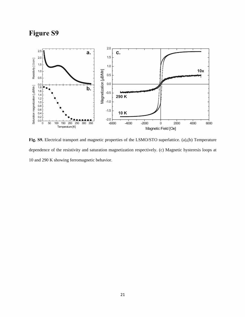
Magnetization and Electrical Transport Measurements:
Electrical transport properties of the sample were measured using the four-point-probe technique, and
are shown in fig. S9(a). The magnetic properties of the sample were measured in a Quantum Design
SQUID Magnetometer (MPMS). Figs. S9(b),(c) show the temperature dependence of the saturation
magnetization (b) and typical magnetization curves at 10 K and 290 K (c) along the [100] direction after
magnetic field cooling at 1 Tesla from 360 K. The values of Tc, resistivity and saturation magnetization
are all consistent with prior studies of LSMO/STO multilayers in this thickness range [22].
High-Resolution Cross-Section STEM Measurements:
In order to verify with a direct imaging technique our previous standing-wave rocking-curve
analysis of concentration depth profiles in a similar STO/LSMO multilayer, as reported previously in ref.
17 of our letter [3], we have performed high-resolution cross-sectional STEM measurements with both
high-angle annular dark field (HAADF) and electron energy loss spectroscopy (EELS), using the
aberration-corrected TEAM 0.5 microscope at the National Center for Electron Microscopy. utilizing a

10
remote operation computer station (RemoTEAM) located at the Electron Microscopy Center at Argonne
National Laboratory. The results of these measurements are shown in fig. S10 below. From the
quantitative analysis of intensities of over 800,000 atomic columns across the full 120 bilayer cross-
section, we have measured the interfacial roughness/interdiffusion between the LSMO and STO layers to
be 1 - 1.5 u.c. This result is further confirmed by directly measuring the EELS chemical signal ratio of
Ti/Mn in several smaller regions of the film, with the LSMO-on-STO interface exhibiting slightly more
interdiffusion/roughness than the STO-on-LSMO interface. Furthermore, the layer thickness is directly
measured to be 4.0 unit cells at the beginning of the growth process, but is found to decrease to 3.4 unit
cells at the 120th bilayer. Thus, the STEM results fully confirm our prior SW-XPS finding that there is a
gradient in the thickness of the STO and LSMO layers from top to bottom of the superlattice [3], and
attest to the accuracy of the multilayer optical constants that we have used for our simulations.

11
References
1. Koster, K. et al. Quasi-ideal strontium titanate crystal surfaces through formation of strontium
hydroxide. Appl. Phys. Lett. 73 (1998) 2920.
2. Huijben, M. et al. Critical thickness and orbital ordering in ultrathin La0.7Sr0.3MnO3 films. Phys.
Rev. B 78 (2008) 094413.
3. Gray, A. X. et al. Interface properties of magnetic tunnel junction La0.7Sr0.3MnO3/SrTiO3
superlattices studied by standing-wave excited photoemission spectroscopy. Phys. Rev. B 82
(2010) 205116.
4. Wannberg, B. Electron optics development for photo-electron spectrometers, Nucl. Instrum.
Methods Phys. Res., Sect. A 601 (2009) 182.
5. Chikamatsu, A. et al. Band structure and Fermi surface of La0.6Sr0.4MnO3 thin films studied by in
situ angle-resolved photoemission spectroscopy. Phys. Rev. B 73 (2006) 195105.
6. Kumigashira, H. et al. In situ resonant photoemission characterization of La0.6Sr0.4MnO3 layers
buried in insulating perovskite oxides. J. Appl. Phys. 99 (2006) 08S903.
7. Plucinski, L. et al. Band mapping in higher-energy x-ray photoemission: Phonon effects and
comparison to one-step theory. Phys. Rev. B 78 (2008) 035108.
8. Papp, C. et al. Band mapping in x-ray photoelectron spectroscopy: An experimental and
theoretical study of W(110) with 1.25 keV excitation. Phys. Rev. B 84 (2011) 045433.
9. A. Bostwick and E. Rotenberg, private communication.
10. Gray, A. X. et al. Probing bulk electronic structure with hard X-ray angle-resolved
photoemission, Nature Mater. 10 (2011) 759.
11. Gray, A. X. et al. Bulk electronic structure of the dilute magnetic semiconductor Ga1-xMnxAs
through hard X-ray angle-resolved photoemission. Nature Mater. 11 (2012) 957.
12. Winkelmann, A., Fadley, C. S. and Garcia de Abajo, F. J. High-energy photoelectron diffraction:
model calculations and future possibilities. New. J. Phys. 10 (2008) 113002.
12
13. Blaha, P., Schwarz, K., Madsen, G., Kvasnicka, D. & Luitz, J. WIEN2k, An Augmented Plane
Wave + Local Orbitals Program for Calculating Crystal Properties (Karlheinz Schwarz, Techn.
Universit. Wien, 2001) ISBN 3-9501031-1-2.
14. Chambers, S. A., Droubay, T., Kaspar, T. C. & Gutowski, M. Experimental determination of
valence band maxima for SrTiO3, TiO2, and SrO and the associated valence band offsets with
Si(001). J. Vac. Sci. Tech. B 22 (2004) 2205.
15. Conti, G. et al. Valence band offset in an LSMO/STO multilayer. unpublished.
16. Tanuma, S., Powell, C. J. & Penn, D. R. Calculations of electron inelastic mean free paths. IX.
Data for 41 elemental solids over the 40 eV to 30 keV range. Surf. Interface Anal. 43 (2011) 689.
17. Perdew, J. P., Burke, K. & Ernzerhof, M. Generalized Gradient Approximation Made Simple.
Phys. Rev. Lett. 77 (1996) 3865.
18. Anisimov, V. I., Solovyev, I. V., Korotin, M. A., Czyzyk, M. T. & Sawatzky, G. A. Density-
functional theory and NiO photoemission spectra. Phys. Rev. B 48 (1993) 16929.
19. Ebert, H., Koedderitzsch, D. and Minár. Calculating condensed matter properties using the KKR-
Green's function method — recent developments and applications. J. Rep. Prog. Phys. 74 (2011)
096501.
20. Jones, R. O. and Gunnarsson, O. The density functional formalism, its applications and prospects.
Rev. Mod. Phys. 61 (1989) 689.
21. Minar, J. et al. Multiple-scattering formalism for correlated systems: A KKR-DMFT approach.
Phys. Rev. B 72, 045125 (2005); Minar, J. et al. Correlation effects in transition metals and their
alloys studied using the fully self-consistent KKR-based LSDA + DMFT scheme. J. Phys.: Cond.
Mat. 23 (2011) 253201.
22. Fitting Kourkoutis, L., Song, J. H., Hwang, H. Y., & Muller, D. A. Microscopic origins for
stabilizing room-temperature ferromagnetism in ultrathin manganite layers. P. Natl. Acad. Sci.
107 (2010) 11682.

13
Figure S1
Fig. S1. (a) Our measurement geometry. (b) The seven different grazing incidence angles (Θ) at which
SWARPES data were collected, corresponding to various positions along the Ti 2p3/2 and Mn 3p rocking
curves. (c) For each value of Θ, an ARPES measurement was collected at 40 different tilt angles (βTOA)
ranging from -20° to +20°, finally yielding corrected data as shown here for the example energy at point 2
expected to be dominated by Mn t2g states.
hv = 833.2 eV
e-
β
a
11.5 12.0 12.5 13.0 13.5 14.00.6
0.7
0.8
0.9
1.0
No
rma
lize
d P
E In
ten
sit
y (
a.u
.)
Grazing Angle (Degrees)
Ti 2p3/2
Mn 3p
A
Rocking Curves
B
CD
EFG
A: Interface
B: Interface
C: Interface (Max.)
D: Bulk/Interface
E: Bulk (Max.)
F: Bulk
G: Bulk
SW Position
b
20
10
0
-10
-20
40
30
20
10
0
800700600500400300200
pixel
Til
t A
ng
le (β
TO
A)
Detector Channel
c

14
Figure S2
Fig. S2. Separating band-dispersions in SWARPES from residual x-ray photoelectron diffraction. (a) A
typical ( , ) map for a fixed value of binding energy , integrated over a 300 meV window
containing the Mn 3d t2g valence states, including an estimated 25% of intensity due to x-ray
photoelectron diffraction (XPD). (b) A corresponding ( , ) XPD map of the Mn 3p core-level
exhibiting only XPD modulation. (c) A simulation of the Mn 3p XPD pattern using dynamical diffraction
(Kikuchi-band) theory. (d) The corrected ( , ) map obtained by normalizing the combined Mn 3d t2g +
XPD spectrum in (a) by the XPD spectrum in (b), so as to more clearly obtain the dispersive electronic
structure of the Mn 3d t2g states, via method described in detail above.
Mn 3d t2g
with XPD
Mn 3p
XPD
Exp.
Mn 3d t2g
Corrected(a) (b) (d)
0 2 4 6
0
2
4
-2
-4
ky
(Å-1
)
kx (Å-1)
0 2 4 6
kx (Å-1)
0 2 4 6
kx (Å-1)
0 2 4 6
kx (Å-1)
Mn 3p
XPD
Theory
(c)

15
Figure S3
Fig. S3. Difference SWARPES patterns between angles F and G that should both be more sensitive to
bulk or central LSMO, with the angular positions relative to the Ti 2p3/2 and Mn 3p rocking curves and
energy positions in a density-of-states shown in the top two panels. The relative magnitude of the
intensity modulations is also indicated.
40
30
20
10
0
800700600500400300200
pixel
40
30
20
10
0
800700600500400300200
pixel
40
30
20
10
0
800700600500400300200
pixel
-12 -10 -8 -6 -4 -2 0
0.0
0.2
0.4
0.6
0.8
1.0
Binding Energy (eV)
1
2
4
5
3
Valence Bands
Rocking Curves
hv = 833.2 eV
T = 20 K
Til
t A
ng
le (β
)T
ilt
An
gle
(β
)
11.5 12.0 12.5 13.0 13.5 14.00.6
0.7
0.8
0.9
1.0
No
rmalized
PE
In
ten
sit
y (
a.u
.)
Grazing Angle (Degrees)
Ti 2p3/2
Mn 3p
FG
40
30
20
10
0
800700600500400300200
pixel
40
30
20
10
0
800700600500400300200
pixel
2 = t2g
5 = VB
Bottom
31= eg
4
100%
-20%
60%
80%
0%
40
30
20
10
0
800700600500400300200
pixel
40
30
20
10
0
x10 -3
100%
-20%
60%
80%
0%
100%
-20%
60%
80%
0%
100%
-20%
60%
80%
0%
1.5 %
0.75 %
0.0 %

16
Figure S4
Fig. S4. As fig. S3, but for the angles C and E exhibiting maximum standing-wave contrast to bulk and
interface.
40
30
20
10
0
800700600500400300200
pixel
40
30
20
10
0
800700600500400300200
pixel
40
30
20
10
0
800700600500400300200
pixel
40
30
20
10
0
800700600500400300200
pixel
-12 -10 -8 -6 -4 -2 0
0.0
0.2
0.4
0.6
0.8
1.0
Binding Energy (eV)
C
1
2
4
5
3
Valence Bands
Rocking Curves
Til
t A
ng
le (β
)T
ilt
An
gle
(β
)
11.5 12.0 12.5 13.0 13.5 14.00.6
0.7
0.8
0.9
1.0
No
rma
lize
d P
E In
ten
sit
y (
a.u
.)
Grazing Angle (Degrees)
Ti 2p3/2
Mn 3p
E
40
30
20
10
0
800700600500400300200
pixel
2 = t2g
5 = VB
Bottom
31= eg
4
hv = 833.2 eV
T = 20 K
100%
-20%
60%
80%
0%
40
30
20
10
0
800700600500400300200
pixel
40
30
20
10
0
x10 -3
100%
-20%
60%
80%
0%
100%
-20%
60%
80%
0%
100%
-20%
60%
80%
0%
6.0 %
2.0 %
-2.0 %
4.0 %
0.0 %

17
Figure S5
Fig. S5. As fig. S3, but for the angles A and B that should both be more sensitive to the LSMO/STO
interface.
40
30
20
10
0
800700600500400300200
pixel
40
30
20
10
0
800700600500400300200
pixel
40
30
20
10
0
800700600500400300200
pixel
-12 -10 -8 -6 -4 -2 0
0.0
0.2
0.4
0.6
0.8
1.0
Binding Energy (eV)
1
2
4
5
3
Valence Bands
Rocking Curves
Til
t A
ng
le (β
)T
ilt
An
gle
(β
)
Mn3p
XPD
11.5 12.0 12.5 13.0 13.5 14.00.6
0.7
0.8
0.9
1.0
No
rmalize
d P
E In
ten
sit
y (
a.u
.)
Grazing Angle (Degrees)
Ti 2p3/2
Mn 3p
B A
40
30
20
10
0
800700600500400300200
pixel
40
30
20
10
0
800700600500400300200
pixel
2 = t2g
5 = VBBottom
31= eg
4
hv = 833.2 eV
T = 20 K
100%
-20%
60%
80%
0%
40
30
20
10
0
800700600500400300200
pixel
40
30
20
10
0
x10 -3
100%
-20%
60%
80%
0%
100%
-20%
60%
80%
0%
100%
-20%
60%
80%
0%
1.5 %
0.75 %
0.0 %

18
Figure S6
Fig. S6. The LDA band structures of (a) the band-insulator STO and (b) the half-metallic ferromagnet
LSMO, as calculated with the Wien2k program. The band gap for STO has been adjusted with a scissors
operator to agree with the experimental indirect bandgap. The experimental band offset in our sample has
been measured using hard x-ray photoemission from core levels and valence bands [15]. The shaded
yellow region is that over which the LSMO bands are expected to be seen in our SWARPES data. The
calculations for LSMO were done in the LDA+U approximation. (c) Projected densities of states for
LSMO, indicating the expected eg, t2g and O 2p makeup. LSMO is assumed to be ferromagnetic here,
even though in our multilayer, it has only weak ferromagnetic order (cf. fig. S9).
Projected DOSs
Spin-down
Spin-upSpin-down
Mn eg
Mn t2g
Expt’l. band offset 3.0 eV
Expt’l. bandgap3.3 eV
dxz+dyz
dxy
dz2dx2-y2
O 2p
Spin-up
dxz+dyz
dxy
a. b. c.

19
Figure S7
Fig. S7. Comparison of experimental angle-averaged DOS-like spectra at angles C (interface) and E
(bulk) with LDA densities of states from the calculations of fig. S6 that have been summed with cross
section and inelastic attenuation corrections over the 4 unit cell/4 unit cell structure of our multilayer.
These show the dominance of LSMO over ca. 0-3 eV, and of STO for greater binding energies. Theory
here is in error by about 4.5 eV for the O-2s dominated band 6 at about 10.5 eV in experiment, but this is
not relevant to our SWARPES data.
Expt.-SWLSMO
Expt.-SWLSMO/STO
STO
LSMO
LSMO
Totaltheory
1
2
4
5 3
Cro
ss S
ect
ion
/Mat
rix-
Elem
en
tW
eig
hte
d D
OS
(a.u
.)
16 14 12 10 8 6 4 2 0Binding Energy (eV)
6
0

20
Figure S8
Fig. S8. Results from fully self-consistent all-electron GGA+U calculations for a 4 u.c. LSMO/4 u.c. STO
multilayer. (a) Side view of the relaxed structure of the superlattice. (b) The layer-resolved total densities
of states (LDOS), with Mn-containing layers at the interface (IF) and center “bulk” layers (IF-1)
indicated. (c),(d) Projected densities of states for Mn summed over (c) the two interfaces IF, (d) the two
center/bulk layers IF-1, and (e) for bulk LSMO. The energy positions at which we have chosen to show
SWARPES results are indicated as 1-5 in (b) and (d). Note that the DOS due to the lowest-lying LSMO
bands near the point R (see fig. S6) are expected to be below those of STO.
Energy (eV)
LDO
S (a
rb. u
nit
s)
TiO2
TiO2
TiO2
TiO2
SrO
SrO
SrO
SrO
(La,Sr)O
(La,Sr)O
(La,Sr)O
(La,Sr)O
MnO2
MnO2
MnO2
MnO2
TiO2
(a) (b) (c)
(d)
(e)
Mn(IF)
Mn(IF-1)
Bulk LSMO
12345
IF-1
IF
12345IF-1
IF
21
Figure S9
Fig. S9. Electrical transport and magnetic properties of the LSMO/STO superlattice. (a),(b) Temperature
dependence of the resistivity and saturation magnetization respectively. (c) Magnetic hysteresis loops at
10 and 290 K showing ferromagnetic behavior.

22
Figure S10
Fig. S10. (a) High resolution HAADF-STEM micrograph of the LSMO/STO sample in cross-section near
the 90th grown layer, with the location of the EELS line scan indicated. (b) Ti/Mn column composition
calculated from the integration of background-subtracted L-edge EELS. (c) Interfacial roughness
calculated from the quantitative HAADF-STEM intensities of 800,000 atomic peaks across the full 120
bilayer cross-sectional sample. Roughness is defined as the RMS variance of the intensity midpoint of
each bilayer transition, with each layer sampled over at least 200 nm. The steep drop-off after 100 layers
is due to a slight bend in the TEM sample from residual stress in the multilayers, and should be ignored.
(d) Layer thickness determined from the quantitative HAADF-STEM intensities of 800,000 atomic peaks
across the full 120 bilayer cross-sectional sample. Layer thickness is defined as the peak-peak distance
between maxima of an envelope function fit to atomic column intensity maxima.
a. b.
c. d.
(a) (b)
(c) (d)
Mn Ti
Co
mp
osi
tio
nR
elat
ive
Ato
mic
Den
sity
Inte
rfac
ial R
ou
ghn
ess
(Un
it C
ells
)
Growth Direction Bilayer Number Growth Direction Bilayer Number
Laye
r Th
ickn
ess
(Un
it C
ells
)STO on LSMOLSMO on STO
STOLSMO
Sub-strate
Sub-strate
Growth Direction Unit Cells
Ti EELS Signal
Mn EELS Signal
![Observation of Polarization Vortices in Momentum Space · the vortices on them, homemade polarization-resolved momentum-space imaging spectroscopy based on Fourier analysis [35] was](https://img.pdfslide.us/doc/110x75/5e70f621bdb80731b82e94e4/observation-of-polarization-vortices-in-momentum-space-the-vortices-on-them-homemade.jpg)