Embed Size (px)
Citation preview

MOLECULAR ENGINEERING OF ELECTRICAL
CONDUCTIVITY OF ORGANIC
NANOFIBER MATERIALS
by
Na Wu
A dissertation submitted to the faculty of
The University of Utah
in partial fulfillment of the requirements for the degree of
Doctor of Philosophy
Department of Materials Science and Engineering
The University of Utah
May 2017
Copyright © Na Wu 2017
All Rights Reserved

The University of Utah Graduate School
STATEMENT OF DISSERTATION APPROVAL
The dissertation of Na Wu
has been approved by the following supervisory committee members:
Ling Zang , Chair 12/01/2016
Date Approved
Feng Liu , Member 12/01/2016
Date Approved
Shelley D. Minteer , Member 12/01/2016
Date Approved
Jennifer S. Shumaker-Parry , Member 12/01/2016
Date Approved
Rajesh Menon , Member 12/06/2016
Date Approved
and by Feng Liu , Chair of
the Department of Materials Science and Engineering
and by David B. Kieda, Dean of The Graduate School.

ABSTRACT
Perylene tetracarboxylic diimide (PTCDI) derivatives, typical n-type organic
semiconductors with high thermal- and photostability, have been extensively investigated
for one-dimensional (1D) self-assembly and their applications in electronic and opto-
electronic devices. Unfortunately, the intrinsically low electrical conductivity of PTCDI-
based materials hinders further development of functions and applications. To solve this
problem, covalently linked electron donor-acceptor (D-A) PTCDI molecules were
designed, synthesized, and assembled into nanofibers in this work. Their electrical
properties and the thermal- and photo-effects have been systematically studied. In
addition to providing an improved understanding of the basic properties of the materials,
these studies also open new and potential applications of the D-A PTCDI nanofibers.
We designed a PTCDI molecule with 1-methylpiperidine (MP) substituted as electron
donor to construct self-doped semiconductors, through one-dimensional (1D) self-
assembly of the molecules into a nanofiber structure. The resultant nanofibers exhibit
much higher conductivity than the other reported PTCDI molecules. The mechanism
studies demonstrate that the MP moieties reduce the adjacent PTCDI core into an anionic
radical, which acts as the n-type dopant in the PTCDI lattice. Such highly conductive
nanofiber materials can be used as chemiresistive sensor for vapor detection of hydrogen
peroxide.
Our further study on the MP-PTCDI nanofibers reveals a persistent photoconductivity

iv
(PPC) effect, which is sustained conductivity after light illumination is terminated.
Systematic study demonstrates the PPC effect is predominantly caused by the D-A
structure of PTCDI. This study helps understand the PPC mechanism, and guide the
design of new material structures for sustained charge separation to further enhance the
photovoltaic and photocatalytic efficiency of organic semiconductor materials.
Thermoactivated conductivity was studied in the nanofiber materials assembled from
other two D-A PTCDI molecules both in the dark and under visible light illumination. A
symmetric n-dodecyl side chain substituted PTCDI nanofiber was used as a control for
the comparative study. The charge transport properties are strongly dependent on the
PTCDI molecular structure and packing states within the nanofibers. The comprehensive
understanding of the thermoactivated conductivity in PTCDI nanofibers can assist in
designing new D-A molecules that can be fabricated into nanofibers to be used as
temperature sensor with increased sensitivity.

To my beloved family

TABLE OF CONTENTS
ABSTRACT ....................................................................................................................... iii
LIST OF TABLES ............................................................................................................. ix
LIST OF ABBREVIATIONS ..............................................................................................x
ACKNOWLEDGEMENTS ............................................................................................. xiii
Chapters
1. INTRODUCTION ...........................................................................................................1
1.1 Introduction of Organic Semiconductors .......................................................... 1 1.1.1 Organic Semiconductors ......................................................................... 1
1.1.2 Charge Transport Mechanisms in Organic Semiconductors ................... 3 1.1.3 Doping of Organic Semiconductors ........................................................ 5
1.1.4 Application of Organic Semiconductors ................................................. 8 1.2 Organic Semiconductors With Donor-Acceptor Structure ............................. 12
1.2.1 The Significance of Donor-Acceptor for Organic Electronics ............. 12
1.2.2 Structure-Property Relationship of Organic Semiconductors ............... 14 1.2.3 Perylene Diimide Derivatives With Donor-Acceptor Structure ........... 17
1.3 Research Goal and Organization of the Dissertation ...................................... 21 1.3.1 Research Goal ....................................................................................... 21 1.3.2 Organization of the Dissertation ........................................................... 23
1.4 References ....................................................................................................... 24
2. CHEMICAL SELF-DOPING OF ORGANIC NANORIBBONS FOR HIGH
CONDUCTIVITY AND POTENTIAL APPLICATION AS CHEMIRESISTIVE
SENSOR ............................................................................................................................45
2.1 Abstract ........................................................................................................... 45 2.2 Introduction ..................................................................................................... 46
2.3 Experimental Section ...................................................................................... 48 2.3.1 Synthesis of N-dodecyl-N’-[(1-methylpiperidine-4-yl) methyl]-
perylene-3,4,9,10-tetracarboxylic Diimide .................................................... 48 2.3.2 Fabrication of Nanoribbons .................................................................. 50 2.3.3 Materials Characterization .................................................................... 50

vii
2.3.4 Current Measurement ............................................................................ 51 2.3.5 Chemical Vapor Sensing Measurement ................................................ 52
2.4 Results and Discussion ................................................................................... 53
2.4.1 Synthesis of MP-PTCDI Molecules and Self-Assembly Into
Nanoribbons ................................................................................................... 53 2.4.2 High Conductivity and Mechanism Study ............................................ 54 2.4.3 Chemiresistive Sensing for Hydrogen Peroxide Vapor Detection ........ 61
2.5 Conclusions ..................................................................................................... 64
2.6 References ....................................................................................................... 64
3. PERSISTENT PHOTOCONDUCTIVITY IN PERYLENE DIIMIDE NANOFIBER
MATERIALS .....................................................................................................................89
3.1 Abstract ........................................................................................................... 89 3.2 Introduction ..................................................................................................... 90
3.3 Experimental Section ...................................................................................... 93 3.3.1 Synthesis of PTCDI Molecules and Fabrication Into Nanofiber
Structures ....................................................................................................... 93 3.3.2 In Situ PTCDI Nanofiber Fabrication on a Substrate ........................... 94
3.3.3 MP-PTCDI Nanofibers Embedded in PEG-PPG-PEG Triblock
Copolymer Matrix .......................................................................................... 95 3.3.4 Materials Characterization .................................................................... 95
3.3.5 Electrical Current Measurement ........................................................... 96
3.4 Results and Discussions .................................................................................. 98 3.5 Conclusions ................................................................................................... 106 3.6 References ..................................................................................................... 107
4. THERMOACTIVATED ELECTRICAL CONDUCTIVITY IN PERYLENE DIIMIDE
NANOFIBER MATERIALS ...........................................................................................130
4.1 Abstract ......................................................................................................... 130
4.2 Introduction ................................................................................................... 131 4.3 Experimental Section .................................................................................... 134
4.3.1 Synthesis of PTCDI Molecules and Fabrication of Nanofibers .......... 134 4.3.2 Materials Characterization .................................................................. 136
4.3.3 Temperature-Dependent Electrical Current Measurement ................. 137 4.4 Results and Discussion ................................................................................. 137 4.5 Conclusions ................................................................................................... 145 4.6 References ..................................................................................................... 147
5. DISSERTATION CONCLUSIONS AND PROPOSED FUTURE WORK ...............162
5.1 Dissertation Conclusions .............................................................................. 162 5.2 Suggestions for Future Work ........................................................................ 164
5.2.1 More Detailed Mechanism Study of PTCDI Molecules With D-A
Structure ....................................................................................................... 165

viii
5.2.2 Applications of PTCDI Molecules With D-A Structure ..................... 165 5.3 References ..................................................................................................... 166

LIST OF TABLES
1.1 Calculated diffusion lengths (LD) for singlet (S) and triplet (T) excitons of crystalline
(C.) and amorphous (Amorph.) films………………………………………………..44
2.1 Comparison of morphology and size of PTCDI-based nanostructures.......................87
2.2 The dipole moment of the liquid analytes tested and the corresponding sensor
response measured at 5% of the saturated vapor concentration..................................88
3.1 The photocurrent on/off ratio, decay time constant of MP-PTCDI nanofibers, and
photocurrent equilibrium time under illumination with various power densities….129
4.1 Activation energy (EA) estimated for the three PTCDI nanofibers in the low and
high temperature range from both the dark current and photocurrent measurement161

LIST OF ABBREVIATIONS
1D One-dimensional
A Acceptor
AFM Atomic force microscopy
BHJs Bulk heterojunctions
C60 Fullerene
CBP 4'-bis(9-carbazolyl)-2,2'-biphenyl
CH-PTCDI N,N-(dicyclohexyl)perylene-3,4,9,10-tetracarboxylic diimide
CTC Charge transfer complex
D Donor
DADP Diacetone diperoxide
DC Direct current
DD-PTCDI N,N’-di(dodecyl)-perylene-3,4,9,10-tetracarboxylic diimide
DIP Di-indenoperylene
DMSO Dimethyl sulfoxide
EA Electron affinity
F4-TCNQ 2,3,5,6-Tetrafluoro-7,7,8,8-tetracyanoquinodimethane
GDM Gaussian disorder model
GIXD Grazing incidence X-ray diffractometry
H2O2 Hydrogen peroxide
HMTD hexamethylene triperoxide diamine
HOMO Highest occupied molecular orbital
IDE Interdigitated electrode
IE Ionization energy
IPA Ion-pair

xi
KPFM Kelvin probe force microscopy
LD Diffusion length
LLR Large lattice relaxation
LUMO Lowest unoccupied molecular orbital
MA-PTCDI N,N-dimethylaniline-substituted perylene tetracarboxylic diimide
MB Microscopic barrier
MO-PTCDI 4-Methoxybenzyl-substituted perylene tetracarboxylic diimide
MP 1-methylpiperidine
MP-PTCDI 1-methylpiperidine-substituted perylene tetracarboxylic diimide
MT-PTCDI N,N-dimethylbutylamine-substituted perylene tetracarboxylic
diimide
NDI Naphthalene diimide
NIR Near-infrared
NPD N, N'-diphenyl-N, N'-bis(1-naphthyl)-1,1'-biphenyl-4,4" diamine
o-DCB Ortho-dichlorobenzene
OFETs Organic field-transistors
OLEDs Organic light-emitting diodes
OSCs Organic semiconductors
P3HT Poly(3-hexylthiophene)
PCB-c-
P3HT Fullerene-capped poly(3-hexylthiophene)
PCBM [6,6]-phenyl-C61-butyric acid methyl ester
PCT Photoinduced charge transfer
PET Photoinduced electron transfer
PPC Persistent photoconductivity
PPV Phenylenevinylene
PTCDA 3,4,9,10-perylenetetracarboxylic dianhydride
PTCDI Perylene tetracarboxylic diimide or Perylene diimide
PtOEP Polycrystalline 2, 3, 4, 7, 8, 12, 13, 17, 18-octaethyl-21H23H-
porphine platinum (II)
RLPF Random localized potential fluctuations
SEM Scanning electron microscope
xii
SubPC Boron subphthalyocyanine
TATP Triacetone triperoxide
TBP Tribenzopentaphene
TCNQ 7,7,8,8-Tetracyanoquinodimethane
TTF Tetrathiafulvalene
UPS Ultraviolet photoelectron spectroscopy
UV Ultraviolet
XRD X-ray diffraction
ZnPc Zinc phthalocyanine

ACKNOWLEDGEMENTS
I would like to express my sincere gratitude to my advisor, Prof. Ling Zang, for his
help, guidance, support, encouragement, and impact in my Ph.D. life. I appreciate him
offering me a chance to study in the field of materials science and engineering. Prof.
Zang is a knowledgeable, rigorous, and gracious mentor for both academics and life. I
have learned a lot from him, including how to do research, how to analyze scientific
problems, and how to present the points. I also appreciate his consistent motivations and
helpful corrections in my presentations and writing. He has also shared with me his
viewpoints on life and career. I am very grateful and happy that I was able to work with
Prof. Zang for the past four and a half years. I also appreciate the time and help from my
other committee members, Prof. Feng Liu, Prof. Shelley D. Minteer, Prof. Jennifer S.
Shumaker-Parry and Prof. Rajesh Menon. Thank you all for your advice, support, and
encouragement
I greatly appreciate all my previous and current group members, Dr. Xiaomei Yang,
Dr. Yanke Che, Dr. Jimin Han, Dr. Ligui Li, Dr. Helin Huang, Dr. Miao Xu, Dr.
Benjamin R. Bunes, Dr. Chen Wang, Paul M. Slattum, Daniel L. Jacobs, Yaqiong Zhang,
and Dr. Li Yu. Thanks for your guidance, training, support, and help.
I would like to thank Dr. Brian van Devener, Dr. Paulo Perez, Dr. Randy Polson,
Brian Baker, Charles Fisher at the Utah Nanofab, Garrett Meeks in the MSE
characterization lab, Dr. Atta M. Arif in the Department of Chemistry, and Dr. Marc. D.

xiv
Porter’s group for their assistance in sample characterization and analysis.
I would also like to thank all the faculty and staff in the Department of Materials
Science and Engineering for their knowledge, guide and help.
I also like to thank all my friends. I appreciate their help.
I would take this chance to thank my mother, father, younger brother, grandmother,
and grandfather, for their persistent love, support, and encouragement all through my life.
At the end, I would like to express my special appreciation to my husband, Zhonghua
Zhan, for his love, selfless support, and encouragement.
This dissertation is based upon work supported by the Department of Homeland
Security, Science and Technology Directorate under Grant (2009-ST-108-LR0005), NSF
(CHE 0931466 and CBET 1502433), the SEED grant of the VP office of University of
Utah (award # 10029849), and USTAR program, I appreciate their support.
Chapter 2 is reprinted with permission from the ACS Applied Materials & Interfaces
2016, 8, 12360-12368.
Chapter 3 is reprinted with permission from the ACS Energy Letters 2016, 1, 906-
912.
Chapter 4 is reprinted with permission from the Journal of Physical Chemistry Letters
2017, 8, 292-298.
CHAPTER 1
INTRODUCTION
1.1 Introduction of Organic Semiconductors
1.1.1 Organic Semiconductors
An organic semiconductor (OSC) refers to organic materials that exhibit
semiconductor properties, mainly consisting of alternating single and double bonds,
leading to high degree of conjugation owing to the presence of π-electrons in their
structures.1-3 In 1977 the first high conducting polymer, chemically doped polyacetylene,
was discovered, which demonstrated that polymers could be used as electrically
conductive materials.4,5 Since then, organic semiconductors have emerged as a promising
field of research and development. Numerous organic semiconductor materials have been
designed and synthesized. They have been used in electronic devices as alternatives to
inorganic semiconductors,6 including organic field-transistors (OFETs),1,7 organic light-
emitting diodes (OLEDs),8,9 photovoltaics,10,11 photodetectors,12,13 lasers,14 and sensors.15-
19 Organic semiconductors are much cheaper than inorganic semiconductors, and in
particular, they are mechanically flexible and solution processable at low temperatures,
making them good candidates for flexible electronic devices.
Organic semiconductors can be classified into two categories according to molecular
weight: small molecules (or oligomers) and polymers. Depending on the preferential

2
transportation of holes or electrons, the organic semiconductors are categorized into p-
type (hole as the majority carrier) and n-type (electron as the majority carrier) materials.1
For p-type OSCs, their highest occupied molecular orbital (HOMO) is relatively higher
(between 4.0 to 5.5 eV), which favors donating an electron, therefore generating holes as
the charge carriers. P-type OSCs have been extensively explored, and some examples are
presented in Figure 1.1. The most studied materials have been acene and thiophene
derivatives.20 For example, pentacene (one of the acene family) is a representative p-type
semiconductor material, which has a remarkable high hole mobility up to 1.1 cm2 V1 s1
on the substrate of alumina, 3.3 cm2 V1 s1 on a soft polymer substrate, and 35 cm2 V1
s1 for a single crystal at room temperature.21 However, the major drawbacks of
pentacene are the insolubility in common solvents and low photostability (due to
photoinduced oxidation), therefore prompting researchers to modify the pentacene
molecule with functional side groups to improve the solubility and stability, while
maintaining the semiconducting features to the maximal.
In contrast to p-type OSCs, the exploration of n-type semiconductors is more
challenging because of their poor ambient stability and low electrical performance. N-
type OSCs are normally electron-deficient small molecular and π–conjugated polymers
with relatively lower energy level of lowest unoccupied molecular orbital (LUMO) (i.e.,
below -3.0 eV ideally).22,23 Figure 1.2 lists some widely studied n-type OSCs. Some
challenges can be found in the development of n-type OSCs. First, the electrical
performance of n-type OSCs is relatively low. Few of the n-type OSCs that have been
reported to date can have an electron mobility comparable to that of amorphous silicon (~
1.0 cm2 V1 s1).24 The low performance of n-type OSCs limits the development of

3
organic electronic devices because both p-type and n-type OSCs are needed for
constructing ambipolar transistors, p-n junctions, and organic circuits, whereas the
mobility of p-type OSCs is much higher.25 Second, due to the low LUMO energy level,
the n-type OSCs are not stable in ambient environment, because the electrons are easily
trapped by O2 and H2O at ambient conditions, or by the hydroxyl groups at the surface of
gate insulators, such as SiO2.23,26 The other challenge of n-type OSCs is that the electron
injections are restrained due to the energy level mismatch between the LUMO of n-type
semiconductors and the Fermi level of electrodes, e.g., Au. In practice, Au electrodes are
still commonly used due to their greater stability than low work-function electrodes (Ca,
Mg, Al, etc.), but with surface modification to reduce the injection barrier.27 To improve
the stability and mobility of n-type OSCs, some strategies for designing high-
performance and ambient-stable n-type OSCs were summarized by the Hu group:28 (1)
functionalization of electron-deficient π-conjugated systems by using fluorine or
fluorocarbon-based functional groups; (2) functionalization of electron-deficient π-
conjugated systems by using electron-withdrawing groups, such as CN, CF3; and (3)
construction of donor-acceptor (D-A) structures.
1.1.2 Charge Transport Mechanisms in Organic Semiconductors
Charge transport properties in organic semiconductors are distinct from the
characteristics in inorganic semiconductors. In inorganic semiconductors, strong ionic or
covalent bonds lead to the formation of three-dimensional crystalline structures with
substantial orbital overlap. Therefore, efficient charge transport can occur through highly
delocalized bands, presenting high charge carrier mobility. However, in OSCs, molecules

4
are organized via supramolecular van der Waals, dipole-dipole, ππ, and hydrogen-bond
interactions.29 The weak intermolecular interactions, closed-shell electronic structures of
the individual organic molecule, and relative disorder of OSCs materials make the charge
transport properties in OSCs different from inorganic semiconductors.
The charge transport mechanism in OSCs is tightly related to temperature.2,30 At low
temperatures (i.e., 100-300 K), band-like charge transport was observed in crystalline
OSCs.31 For instance, the intrinsic transport of field-induced charges on the surface of a
single crystal of rubrene has been studied, and it has been noted that its mobility
increased with decreasing temperature.32 At room temperature or higher, it is generally
believed that the charge mobility of semiconducting organic materials is determined by a
hopping transport mechanism,2,33 where charges jump from site to site, because the
charge carriers turn to be more conductive to localize at higher temperature due to the
reduced effective bandwidth. Electrical conduction by hopping is still not clear. One of
the most clearly understood mechanisms is the polaronic transport, a phonon-assisted
hopping process.34 Upon adding or removing an electron from a molecule, associated
with the resultant molecular skeleton changes because of the readjustment of the
individual bond lengths, a polaron forms. The polaron is a quasiparticle by electron-
phonon coupling, the binding energy of which comes from local geometric relaxations
and increased polarization of the surrounding medium. The polaron hopping is thus a
charge associated with a molecular distortion.35
In addition to the effect of temperature, the molecular arrangement patterns also
influence the charge transport mechanism. The Weng group observed the photogenerated
free carriers, rather than exciton at room temperature, in highly crystalline Zinc

5
phthalocyanine (ZnPc films) prepared by weak epitaxy growth method. The band-like
electronic feature of ZnPc thin film is from the effective intermolecular interactions
between the cofacially-stacked π-conjugated ZnPc molecules.36
1.1.3 Doping of Organic Semiconductors
Organic semiconductors have an intrinsic smaller charge carrier mobility and lower
performance compared to inorganic semiconductors due to the closed-shell electronic
structures of the individual organic molecules, weak intermolecular interactions, and
comparatively disordered structure.29,37 Electrical doping of OSCs has emerged as an
effective strategy to improve the performance of organic electronic devices and to extend
the range of functionality. In particular, controllable doping of OSCs can make great
technological breakthroughs like what happened in the inorganic semiconductor industry,
which constitutes the basis for electronic devices.38,39
The basic doping fundamentals in OSCs are similar to those in inorganic
semiconductors, that is to say, extra mobile charge carriers in OSCs matrix are produced
by electron donors or acceptors (Figure 1.3).40 Theoretically, in OSCs doping, dopants
are added into the organic semiconductor matrix, which will transfer electrons to the
LUMO states of OSCs (n-type doping) or remove electrons from the HOMO states of
OSCs to generate holes (p-type doping). The dopants can be small molecules or atoms,
such as iodine, bromine, Lewis acids, lithium, cesium, and strontium atoms. However,
these small dopants show a strong tendency to diffuse, leading to a falling performance of
electronic devices.6 To resolve these problems, molecular doping, of which larger organic
molecular electron acceptors or donors are dopants, has been developed in the past

6
decades as a replacement for traditional doping.6,38,39 For example, strong electron
acceptor F4-TCNQ has been widely used as a p-type dopant. For example, F4-TCNQ
was doped in ZnPc to enhance the conductivity and reduce the Seebeck coefficient.41
With this methodology, stable and high performance electronic devices have been
designed and developed.
In molecular doping, ion-pair (IPA) and ground-state charge-transfer formation are
widely considered as the two fundamental interaction mechanisms between dopant and
OSCs matrix (Figure 1.4).38 For the IPA mechanism, electron transfer happens between
dopants and OSCs, giving rising to the formation of anion and cation (the ion pair).
Taking p-type doping as an example, when the electron affinity (EA) of the acceptor is
equal or higher than the ionization energy (IE) of the OSCs, one electron is transferred
from the HOMO of the OSCs to the LUMO of the acceptor, followed by formation of an
acceptor anion and an OSC cation. The IPA mechanism of n-type doping is similar, but
the electron is transferred from the HOMO of the n-type dopant to the LUMO of the
OSC.
Another mechanism that generates mobile charge carrier density in molecularly
doped OSCs is dependent on the establishment of ground state charge transfer complex
(CTC).38,42 Interacting with dopants, new occupied bonding and empty antibonding
orbitals are formed from the rearranging of the frontier molecular orbitals of an OSC
molecule and a dopant. The new energy levels of CTC (ECTC, H/L) are determined by the
contribution of parent OSC and dopant as descripted by the Hückel-type model (Equation
1.1, for p-type doping), where HOSC is the HOMO level of OSC, Ldop is the LUMO level
of the dopant, and β is the resonance integral. In the case of p-type doping, if IE of the

7
CTC is higher and its EA lower than the IE of the OSC, the electrons will be reorganized,
creating a filled level below the transport manifold of the OSC and an empty one above.
Subsequently, the CTC is ionized to form a separated mobile hole in the OSC. In other
words, the CTC acts as a dopant. The energy levels and the corresponding density of
states (DOS) of IPA and CTC molecular doping processes are sketched in Figure 1.4.38,43
𝐸𝐶𝑇𝐶,
𝐻𝐿
=𝐻𝑂𝑆𝐶 + 𝐿𝑑𝑜𝑝
2± √(𝐻𝑂𝑆𝐶 − 𝐿𝑑𝑜𝑝)
2+ 4𝛽2 1.1
Two important factors are generally considered in doping OSCs, one is the position of
the Fermi level after doping.6,40 Doping will shift the Fermi level toward the transport
level of the OSCs. The position of the Fermi level after doping can be examined from the
Seebeck effect as seen in Equation 1.2.41,44
𝑆(𝑇) =𝑘𝐵
𝑒[(
𝐸𝐹(𝑇) − 𝐸𝑢
𝑘𝐵𝑇) + 𝐴] 1.2
where S is the Seebeck coefficient. Eu is the energy level of transport states and EF is the
Fermi-level. A is a numerical factor, kB is the Boltzman constant, T is the temperature,
and e is the elementary charge. Ultraviolet photoelectron spectroscopy (UPS) can be used
to determine the distribution of transport states (Eu). Therefore, the position of the Fermi
level after doping can be measured, allowing for a deeper understanding of the doping
and realizing controllable doping. The other is the doping efficiency. Doping efficiency is
strongly related to the EA and IE of dopant (or CTC) and host OSCs.

8
1.1.4 Application of Organic Semiconductors
Organic semiconductors are alternative to conventional inorganic semiconductors in
some areas and have been used commercially, such as in xerography, sensor, lighting,
and display. OSCs are cheaper, flexible, and easy to process. Numerous investigations
and developments of OSCs application have been reported. Herein, some typical
applications based on OSCs will be briefly reviewed, particularly the applications in
electronic devices including field-effect transistors, light emitting diodes, photovoltaic
systems, and electrical sensors.
1.1.4.1 Organic Field-Effect Transistors
Organic field-effect transistors (OFETs) have been fabricated with various device
geometries.1,7 The most commonly used device geometry is bottom gate with top drain
and source electrodes. The active organic FET layer can be deposited onto the substrate
by thermal evaporation, solution-process coating, printing, or electrostatic lamination.
Field-effect mobility is one of the key parameters considering OFETs’ performance,
which is largely relevant to the electronic properties of OSCs materials. The field-effect
mobility (μ) was lower than 103 cm2 V1 s1 about 25 years ago, but it has increased to
about 1-10 cm2 V1 s1 for some OSCs due to advancements in molecular design,
material processing techniques, and device architecture. OFETs have been used in
displays, simple circuits, and chemical and biological sensors.

9
1.1.4.2 Organic Light-Emitting Diodes
An organic light-emitting diode (OLED) is a device that transforms electrical power
into light. In a typical OLED device, the active OSCs are located between two suitable
electrodes. Single-layer of heterojunctions of OSCs can be employed in OLED
devices.9,45,46 Heterojunction OLEDs are more widely investigated and developed
because of the higher efficiency than single-layer ones. A typical bilayer OLED involves
cathode, emissive layer, conductive layer and anode. The basic working principle of an
OLED is that when a bias voltage is applied to the electrodes, electrons are injected from
the cathode to anode through giving electrons to emissive layer and removing electrons
from the conductive layer. The holes in the conductive layer move to the emissive layer,
where the recombination of the electron and hole results in the formation of a photon, of
which the frequency is determined by the energy gap of the HOMO and LUMO levels of
emitting molecules. The efficiency of an OLED can approximately be deduced by
Equation 1.3,6 where ηexternal is the final efficiency of the device, bI is the carrier balance,
which can be adjusted by choosing suitable blocking layers in multilayer OLED devices,
U is the operating voltage, and ηrecomb is the quantum efficiency of carrier recombination,
determined by the ratio of radiative recombination of excitons to the total number of
excitons, and ηoptical is the efficiency of the optical outcoupling from the device.
Researchers have focused on the materials design and devices structure improvement to
enhance the efficiency of the OLED. Usually, doped OSCs in the OLEDs can improve
the charge carriers injection, leading to lower driving voltage, thus to an enhanced power
efficiency.47

10
𝜂𝑒𝑥𝑡𝑒𝑟𝑛𝑎𝑙 = 𝑏𝐼
ℎ𝑣
𝑒𝑈𝜂𝑟𝑒𝑐𝑜𝑚𝑏 𝜂𝑜𝑝𝑡𝑖𝑐𝑎𝑙 1.3
1.1.4.3 Organic Photovoltaics
Similar to the application in OLEDs, OSCs have also been extensively used in
photovoltaic devices (solar cells), which are devices to convert light into direct current
(DC) electricity. Being excited by light with energy larger than the band gap of the OSCs,
excitons are formed, and then excitons are separated into free electrons and holes, which
move in different directions to cathode and anode, converting solar energy into DC
electricity.10 Unlike inorganic solar cells, the exciton is generated in OSCs as a tightly
bound electron-hole pair because of the strong Coulomb attraction between the electron
and hole due to the low dielectric constant of organic materials.48-51 Consequently,
improving the charge separation efficiency is a key issue of organic solar cells. To meet
this challenge, bulk heterojunctions (BHJs) of OSCs have been developed,11,52,53 which
have an absorber layer consisting of a blend of donor and acceptor materials in nanoscale.
The advantage of the donor-acceptor (D-A) heterojunction is to accelerate the electron
and hole separation rate. The electron-hole binding energy is evaluated to be 0.35-1.0
eV,11 which is larger than the thermal energy at room temperature (kBT ~ 0.026 eV) by an
order of magnitude. Therefore, D-A structure is constructed to facilitate the generation of
free charge carriers at the D-A interface through the driving force created by the energy
level offset between donor and acceptor.

11
1.1.4.4 Organic Electrical Sensors
The other important application of OSCs is in electrical sensors,15,54 which have been
extensively used in industrial, environmental, and medical areas as well as public safety.
Sensitivity, selectivity, and the response and recovery time are among the important
criteria for sensors. Traditional inorganic electrical sensors have already been widely
studied and commercially used. Unfortunately, inorganic electrical sensors have
limitations in selectivity and require high operation temperature.15 Especially for the
sensors that are made of metal oxide semiconductors, the dramatic response to humidity
(moisture) inhibits the application in open environments. OSCs provide alternative
materials for sensor development that possess much more flexibility for structural and
property modification in order to improve the sensor selectivity. In principle, the
selectivity is achieved through molecular recognition based on analyte-OSC interactions,
which include hydrogen bonding, dipole-dipole interactions, van der Waals interactions,
and charge transfer.55 When exposed to analytes, the electrical properties of OSC
materials can be affected through charge transfer interaction, charge trapping or doping,
adjusting the charge injection or extraction behavior at the electrode/OSCs interfaces, or
changing the molecular arrangement of OSCs. The Zang group has developed a series of
organic nanofibril chemiresister sensors, which were able to detect trace vapor of
explosives,18 amines,19 hydrogen peroxide,17 alkane,16 and so on. These nanofibers,
fabricated from self-assembly of OSC molecules, can provide exciton or electron
transport channel as sensing materials, and have the potential to amplify the output signal
due to the long-range exciton or electron migration along the one-dimensional well-
organized nanofibers.56,57 Organic field-effect transistors (OFETs) are also excellent

12
transducers for sensing because amplified signals can be attained.58 According to the
working principle of OFET when analytes interact with channel materials, the signal can
be modified by the gate voltage. If the gate dielectrics are used as the sensitive layer, a
small change of the effective gate voltage induced by analyte may lead to a pronounced
variation of channel current.15 OFET sensors can be applied for detecting chemicals in
gas (vapor) phase, or analytes in solution or biological system with high sensitivity.
1.2 Organic Semiconductors With Donor-Acceptor Structure
1.2.1 The Significance of Donor-Acceptor for Organic Electronics
Modification of organic semiconductors with electron donor-acceptor (D-A) structure
or interface is an interesting research topic, because it is an efficient strategy to achieve
high conductivity of OSC materials,17,18,59 or to construct higher performance electronic
devices.60 The efficiency and rate of electron transfer between donor and acceptor are
determined by the electron donating and accepting abilities in the D-A system, and the
distance, spatial orientation, and flexibility between the donor and acceptor moieties.61 In
this section, we will discuss the significance of OSCs with D-A system.
First, lower band gap OSCs can be synthesized by incorporation of D-A system.62,63
In general, the HOMO level of OSCs shifts to higher energy level by the introduction of
strong electron donating groups, whereas the presence of strong electron accepting
groups lowers their LUMO levels. The OSCs with low band gaps have broadened
absorption from the ultraviolet (UV) to the near-infrared (NIR) region, enabling fully
utilizing the solar energy for solar cells64 and realizing broadband photo-detection.65
Second, the significance of D-A system in OSCs is to enhance the charge generation

13
and separation. Charge generation is achieved through the formation of charge-transfer
complex (CTC) or photoinduced charge transfer (PCT). It has been demonstrated that a
charge transfer complex can be formed when an electron donor (D) molecule or moiety
has low ionization potential and an electron acceptor (A) molecular or moiety has
relatively high electron affinity (Equation 1.4),66 where +, - represent the partial charge
distributed between the D and A part. Upon association, some new properties arise in the
CTC, for example, new charge-transfer (CT) bands are formed. Optical spectroscopy is a
powerful technique to characterize CT bands, such as UV-vis absorption spectroscopy,
luminescence spectroscopy, electron paramagnetic resonance spectroscopy, resonance
Raman spectroscopy, positron annihilation spectroscopy (PAL) 67 and so on.
𝐷 + 𝐴 ↔ [𝐷𝛿+ ∙ 𝐴𝛿−] 1.4
A charge transfer complex may assist the generation of charge carriers when an
electric field is applied on the D-A compound, resulting in dramatic enhancement in
conductivity.68 The enhanced conductivity is attributed to the charge generation and
subsequent disassociation with D-A structure or D-A interface.69 Tetrathiafulvalene
(TTF) - 7,7,8,8-Tetracyanoquinodimethane (TCNQ) is a prototype charge-transfer
compound.70 The complex is formed in solution and can be precipitated and grown into a
crystalline solid (Figure 1.5 a).71 In a TTF-TCNQ crystal, TTF and TCNQ are arranged in
separated linear chains, then aligned interspaced (Figure 1.5b).72 TCNQ is an acceptor
molecule with electron affinity of 2.88 eV which can be easily reduced to the anion
radical TCNQ when it interacts with electron donors, such as TTF.

14
Photoinduced charge transfer (PCT) is mainly about photoinduced electron transfer
(PET),18,69,73 which is an excited electron transfer process by which an excited electron is
transferred from donor (D) to acceptor (A). When an organic molecule is excited by
photon absorption, an electron in a ground state orbital can be excited to a higher energy
orbital. On one hand, this excited state leaves a vacancy in a ground state orbital that can
be filled by an electron donor. On the other hand, it generates an electron in a high energy
orbital, which can be donated to an electron acceptor. In addition to the PET process,
researchers have also discovered a photoinduced hole transfer process, of which a hole is
generated through photoexcitation of an acceptor, followed by transfer to the ground state
donor.74 This PCT process has attracted great interest because of their fundamental role in
applications such as solar cells and artificial photosynthetic systems.
Regarding the research on the D-A OSCs, two categories of D-A structures can be
developed. One is the covalent D-A molecules, where D and A parts are constructed in
one molecule via organic synthesis techniques; the other is the noncovalent D-A
structure, where two or more donor and acceptor molecules associate to form D-A
interface by molecular engineering, such as co-crystallization, blending, and surface
coating, etc.69
1.2.2 Structure-Property Relationship of Organic Semiconductors
It has been demonstrated that the electronic properties of OSCs are tightly related to
their molecular and supramolecular structure. In addition, the performance of the
electronic devices based on OSCs depends on the morphology of these active materials.
In the previous section, we discussed the significance of D-A system. Organic

15
semiconductors with a D-A system can have a narrower band gap and enhanced charge
carrier generation and separation efficiency. However, there are some drawbacks for
some simple D-A systems, particularly in polymers. One is the absence of control over
the orientation of molecular components because conventional synthesis (or
polymerization) restricts the regioselectivity when asymmetric monomers are utilized.75
As a result, the limit in the regioselectivity would influence the intermolecular π-stacking
interactions, leading to inefficient charge transport.76,77 Another drawback is the limited
solubility of organic materials.78 To overcome the drawbacks and increase the D-A
interactions, organic semiconductors with multiple alternating donor or acceptor groups
were designed to control both the structural and electronic properties. In Watkin group’s
work, A-D1-A-D1 and A-D1-A-D2 structures were compared. By using two different
donor fragments (D1 and D2) in the polymer semiconductor, it demonstrated improved
intermolecular π-stacking interactions and therefore enhanced charge-carrier mobility.
The solar cells based on A-D1-A-D2 polymer exhibited short-circuit current densities
twice as high as the ones fabricated with simple A-D1-A-D1 polymer, but still having the
similar open-circuit voltage.75 Patil et al. have also designed A1-D-A2-D polymer to
fabricate OFETs and had a remarkable improvement in electron mobility due to the
optimized chain packing and resultant large crystalline domains formation in solid state.79
In addition, molecular ambipolar D-A1-A2 organic semiconductors were synthesized to
suppress the back electron transfer through the cascade energy levels.61
Charge mobility is one of the most fundamental properties of semiconductors. The
charge mobility is strongly associated with the degree of long range order. In organic
semiconductors, the charge (free charge carriers, molecular excited state, or exciton)

16
diffusion length (LD) is important regarding the mobility. Taking the exciton as an
example, it has been established that exciton transport is a function of the extent of
crystalline order.80-82 Lunt et al. have measured the exciton diffusion lengths of several
organic semiconductor thin films which are widely used in organic electronic devices by
spectrally resolved photoluminescence quenching. The measured diffusion length values
can be found in Table 1.1. The exciton diffusion length was revealed to be strongly
related to the molecular stacking habit and the existence of dimer states in polycrystalline
thin film.81
Controlling the morphology of the active layer is an important strategy for increasing
the efficiency of electrical devices based on OSCs. For example, a lot of research works
were focused on optimization of organic materials morphology to enhance BHJ
photovoltaic efficiency.11 The ideal structure of a BHJ solar cell is schematically
descripted in Figure 1.6.10 Interspaced donors and acceptors are arranged within an
average length of exciton diffusion (about 10-20 nm), making sure the exciton can reach
the D-A interface to initiate the charge separation. In addition, the two D-A phases are
interlaced in percolated patterns to ensure efficient charge carrier transport with reduced
recombination. There are many methods to modify the BHJ morphology, including
adjusting the concentration and ratio of the donor and acceptor in solution, processing
solvent, casting methods, drying rate, and post film treatment like thermal annealing and
solvent annealing.83 Generally, these methods can improve the organic materials’
crystallinity, and control phase separation in the blend morphology to ensure continuous
charge transport pathway to the electrodes. For example, the efficiency of a P3HT/C61-
PCBM solar cell can be increased from 0.83% to nearly 5% when heating the film at 150

17
°C for 30 min.84
Besides the above methods, controlled self-assembly of organic semiconductors is the
most desirable way to approach the ideal BHJ solar cell structure. A molecule PCB-c-
P3HT, covalent linking a P3HT chain with fullerene, was designed and self-assembled
into nanowires in an ortho-dichlorobenzene (o-DCB) solution. In contrast to
noncovalently mixed P3HT polymer:fullerene blends, the covalent copolymer PCB-c-
P3HT can self-assemble to produce more defined interfaces of donor and acceptor in thin
films. Additionally, the crystallization of the P3HT core and alignment of the PCB into
wires allows for high delocalization of charges and effective transport for carriers, giving
rise to high dark current and photocurrent.85
1.2.3 Perylene Diimide Derivatives With Donor-Acceptor Structure
Perylene tetracarboxylic diimide (PTCDI) derivatives have been extensively studied
and used as industrial dyes and pigments since 1912 because they are chemically inert
and possess high thermal- and photostability.86 Figure 1.7 is the chemical structure of
PTCDI. The imide sides (R group) or bay positions (the 1, 6, 7, 12 positions) can be
modified with various substituents to obtain different PTCDI molecules with different
chemical and physical properties.
Later, PTCDIs’ chemical and physical properties were further investigated. It was
found that PTCDIs present a relatively low reduction potential (ca. -1.0 V for the first
half-wave reduction potential and -1.2 V for the second half-wave reduction potential vs
the ferrocene/ferrocenium [FeCp2+/0] redox couple) and low electron affinity (about -3.9
eV for unmodified PTCDIs, comparable to fullerene [C60] and its derivatives),87-89

18
combining with their superior thermal- and photostability, which enables their use as
electron acceptors or n-channel materials in electronic and optoelectronic devices.
Moreover, PTCDI molecules have also been widely studied in fundamental research on
OSCs’ charge transport mechanism, photo-induced energy and electron transfer
processes.90
In this dissertation, we focus our research on the electrical properties and potential
applications of imide substituted PTCDIs and their corresponding self-assembled
nanofibers. More detailed properties of PTCDIs will be discussed in the following
sections.
1.2.3.1 Molecular Structural Properties of PTCDIs
The perylene diimides present flat π-systems as established by X-ray diffraction of
their single crystals. The frontier orbitals of perylene diimide are presented in Figure 1.8.
It has been proven that the imide substituent has a negligible influence on the electronic
properties of perylene bisimides because the nodes in the HOMO and LUMO at the imide
positions of perylene diimides minimize the electronic coupling between perylene
aromatic core and substituents,57,86 for example, there is a less than 0.1 eV change on a
PTCDI’s LUMO upon switching from phenyl to perfluorophenyl on the imide
positions.91 It is beneficial to modify the PTCDI molecules to adjust their solubility,
control the molecular packing patterns as well as comparatively study PTCDI molecules
with different substituents without significantly changing the perylene diimide core’s
electronic properties.

19
1.2.3.2 Self-Assembly of PTCDI Molecules into One-Dimensional Nanostructures
PTCDI molecules can be self-assembled into well-defined one-dimensional (1D)
nanostructures by controlling the solution processing conditions. The Zang group has
conducted enormous pioneering works on the 1D self-assembly of PTCDI molecules and
found that the 1D self-assembly is a thermodynamic process of maximizing the
longitudinal π-π stacking over the lateral association to form bulky aggregates due to the
hydrophobic interaction among the side chains.56,92-94 Depending on the molecular
structure and geometry, the effective self-assembly of PTCDI molecules into 1D
nanostructures can be completed via rapid solution dispersion, phase transfer, vapor
diffusion, seeded growth, and sol-gel processing.56
Crystal structures of PTCDIs have been extensively studied to help understand 1D
PTCDI nanostructures. Most crystal structures of PTCDIs with symmetrical n-alkyl
imide substitutes exhibit primitive triclinic unit cells. Taking the PTCDI-C8H17 (PTCDI-
C8) molecule as an example, the packing alignment of the PTCDI-C8 molecule in the
unit cell is schematically shown in Figure 1.9. The PTCDI-C8 molecules exhibit slipped
π-π stacking in the [100] direction with the shortest vertical distance at around 3.34 Å to
3.55 Å between the atomic planes of neighboring PTCDI-C8 molecule.95 As the
modification of substituted groups at imide sides with larger groups, the rotational offsets
have been observed leading to different distorted π-π stacking patterns. N,N-
(dicyclohexyl)perylene-3,4,9,10-tetracarboxylic diimide (CH-PTCDI) is a symmetric
molecule with both sides substituted with cyclohexane groups, which shows a flip-flap
stacking to minimize the steric hindrance between the cyclohexyl side-chains.96

20
1.2.3.3 PTCDI Nanofibers With Donor-Acceptor Structure
PTCDI nanofibers with D-A structure have attracted much research effort. A series of
nanofiber structures modified with different D-A interfaces have been developed via
covalent links or noncovalent interaction.
In covalently linked D-A molecules, it is difficult to obtain continuous one-
dimensional stacking because the donors and acceptors prefer to stack with each other
due to the charge transfer interaction between them.97 Furthermore, charge recombination
occurs easily between D+ and A- in the bulk-mixed phase of D and A. To solve this issue,
amphiphilic D-A type PTCDI molecules (e.g., those with long alkyl chain in one imide
side and the donor group in the other imide side) were designed and synthesized.17,69,96
This type of PTCDI molecules can be fabricated into well-defined 1D nanostructures
driven by the π-π stacking and side chains interactions.
Noncovalent D-A structure can be constructed through blending the PTCDI
molecules (usually as the acceptor) with donor molecules, or controlled surface coating
of PTCDI nanofibers with donor molecules, which offers more structure diversity and
tailorability in comparison to the approach using covalent PTCDI D-A molecules. In
particular, the morphology of D and A parts, as well as the interface, can be improved
through postcoating treatments, such as solvent annealing or high temperature annealing.
For the surface coating, appropriate donor molecules design can enhance the D-A
interaction. The Zang group has demonstrated that the modification of the
tribenzopentaphene (TBP) donor molecules with large side groups can prevent
intermolecular π-π stacking of the donor molecules, leading to uniform molecular
distribution of donors onto the PTCDI nanofibers, giving rise to a higher photocurrent

21
than PTCDI nanofibers coated with TBP modified with small side groups.98
1.2.3.4 Charge Transfer in PTCDI Nanofibers With D-A Structure
PTCDI molecules with D-A structures are used as the building blocks to construct 1D
nanomaterials featuring higher conductivity (Figure 1.10). First, the ordered 1D π-π
stacking in the PTCDI nanofibers favors the electron transfer through co-facial
intermolecular π-delocalization.56,57 As a result, relatively higher conductivity can be
attained in the PTCDI 1D nanostructures due to efficient electronic coupling.
Second, PTCDI derivatives are acceptors in the D-A system, and can take part in a
variety of excited-state electron transfer processes, as illustrated in Figure 1.11. In
addition to the photoinduced charge separation, strong electron donors can also initiate
charge separation in the dark though steady-state charge-transfer between donors on one
molecule and PTCDI cores on the adjacent molecule, as demonstrated as the
intermolecular charge transfer. In this process, the donor moieties with strong electron
donating capability (evaluated by the oxidation potentials) and nucleophilicity can reduce
PTCDI central cores into the anionic radicals.
1.3 Research Goal and Organization of the Dissertation
1.3.1 Research Goal
Perylene tetracarboxylic diimide (PTCDI) derivatives, a typical n-type organic
semiconductor with high thermal- and photostability, have been extensively investigated
for one-dimensional (1D) self-assembly and their applications in electronic devices.
However, it’s still challenging to have high performance electronic and optoelectronic

22
devices (or systems) with PTCDI-based material due to intrinsically limited properties of
organic semiconductors, such as low conductivity. The goal of this dissertation is to
design new PTCDI molecules with covalent donor-acceptor (D-A) structure, study their
optical and electrical properties, and explore their applications in organic electronics and
photocatalysis.
The intrinsically low electrical conductivity of organic semiconductors, due to
properties such as the closed-shell electronic structures of the individual organic
molecules, and weak intermolecular interactions, hinders further development and more
widespread applications. In the first part of this dissertation, we developed a chemical
self-doping method that can increase the electrical conductivity through a one-
dimensional stacking arrangement of donor-acceptor (D-A) PTCDI molecules. The D-A
structure is based on 1-methylpiperidine-substituted perylene tetracarboxylic diimide
(MP-PTCDI), of which the MP moiety is a strong electron donor, and can form a charge
transfer complex with the PTCDI moiety on the other molecule (acting as the acceptor) of
an adjacent stacked molecule, generating anionic radicals of PTCDI (electron). Upon
self-assembling into 1D nanostructure (specifically nanoribbons), the electron generated
is delocalized along the long axis of PTCDIs through columnar π-π stacking, leading to
enhancement in conductivity. The resultant PTCDI radicals function as n-type dopants
located in the lattice of PTCDI crystals, in contrast to interstitial doping.
In the second part of this dissertation, the specific chemical and physical properties of
PTCDI derivatives with D-A structure were studied in detail, particularly the persistent
photoconductivity (PPC) and thermoactivated electrical conductivity in PTCDI nanofiber
materials. The PPC is the sustained electrical conductivity after light illumination is

23
terminated. A comprehensive understanding of the PPC effect in PTCDI nanofibril
materials will enable us to explore and enhance their optoelectronic applications, such as
photovoltaics and photocatalysis. The study of temperature-dependent conductivity in
PTCDI nanofibers provides us deeper insight into the charge transport mechanism, which
will be conducive to developing more sensitive organic temperature sensors.
1.3.2 Organization of the Dissertation
The remainder of the dissertation contains the following four chapters.
Chapter 2 demonstrates research on chemical self-doping of MP-PTCDI nanoribbons
for high conductivity and their application as a chemiresistive sensor for vapor detection
of electron deficient chemicals. It includes the new PTCDI molecule design, the detailed
chemical self-doping mechanism to achieve high conductivity, and chemiresistive
sensing for hydrogen peroxide vapor detection.
Chapter 3 focuses research on persistent photoconductivity (PPC) effect in PTCDI-
based nanofiber materials. This chapter demonstrates the PPC effect with respect to
different temperature, illumination power densities, molar amount, and morphology of
the PTCDI film. The comparative study of PPC effect in various PTCDI molecules
modified with different electron-donating moieties was conducted with the aim to
investigate the influence of electron donor-acceptor interaction on the PPC.
Chapter 4 presents the research of the thermoactivated conductivity in PTCDI
nanofibers. We studied the temperature activated charge transport within the PTCDI
nanofibers with D-A interfaces. For comparison, the study was also performed on a
control sample, which was a nanofiber fabricated from a symmetric PTCDI molecule

24
with both sides modified with n-dodecyl chain. D-A structure helps create disorder
regarding both the charge-transfer and dipole-dipole interactions between stacked
molecules, and the increased disorder enlarges the activation barrier, enabling larger
sensitivity to temperature.
Chapter 5 summarizes the major results and conclusions from all the research works
described above, and provides some perspective for future research on PTCDI
nanofibers, particularly those with D-A structure.
1.4 References
(1) Facchetti, A. Semiconductors for Organic Transistors. Mater. Today 2007, 10, 28-37.
(2) Coropceanu, V.; Cornil, J.; da Silva Filho, D. A.; Olivier, Y.; Silbey, R.; Brédas, J.-L.
Charge Transport in Organic Semiconductors. Chem. Rev. 2007, 107, 926-952.
(3) Marrocchi, A.; Facchetti, A.; Lanari, D.; Petrucci, C.; Vaccaro, L. Current
Methodologies for a Sustainable Approach to π-Conjugated Organic Semiconductors.
Energy Environ. Sci. 2016, 9, 763-786.
(4) Shirakawa, H.; Louis, E. J.; MacDiarmid, A. G.; Chiang, C. K.; Heeger, A. J.
Synthesis of Electrically Conducting Organic Polymers: Halogen Derivatives of
Polyacetylene, (CH)x J. Chem. Soc., Chem. Commun. 1977, 578-580.
(5) Chiang, C. K.; Fincher, C. R.; Park, Y. W.; Heeger, A. J.; Shirakawa, H.; Louis, E. J.;
Gau, S. C.; MacDiarmid, A. G. Electrical Conductivity in Doped Polyacetylene. Phys.
Rev. Lett. 1977, 39, 1098-1101.
(6) Walzer, K.; Maennig, B.; Pfeiffer, M.; Leo, K. Highly Efficient Organic Devices
Based on Electrically Doped Transport Layers. Chem. Rev. 2007, 107, 1233-1271.
(7) Sirringhaus, H. 25th Anniversary Article: Organic Field-Effect Transistors: The Path
Beyond Amorphous Silicon. Adv. Mater. 2014, 26, 1319-1335.
(8) Kamtekar, K. T.; Monkman, A. P.; Bryce, M. R. Recent Advances in White Organic
Light-Emitting Materials and Devices (WOLEDs). Adv. Mater. 2010, 22, 572-582.
(9) D'Andrade, B. W.; Forrest, S. R. White Organic Light-Emitting Devices for Solid-
State Lighting. Adv. Mater. 2004, 16, 1585-1595.
(10) Günes, S.; Neugebauer, H.; Sariciftci, N. S. Conjugated Polymer-Based Organic
25
Solar Cells. Chem. Rev. 2007, 107, 1324-1338.
(11) Scharber, M. C.; Sariciftci, N. S. Efficiency of Bulk-Heterojunction Organic Solar
Cells. Prog. Polym. Sci. 2013, 38, 1929-1940.
(12) Zhang, H.; Jenatsch, S.; De Jonghe, J.; Nüesch, F.; Steim, R.; Véron, A. C.; Hany,
R. Transparent Organic Photodetector Using a Near-Infrared Absorbing Cyanine Dye.
Sci. Rep. 2015, 5, 9439.
(13) Lee, K.-H.; Leem, D.-S.; Castrucci, J. S.; Park, K.-B.; Bulliard, X.; Kim, K.-S.; Jin,
Y. W.; Lee, S.; Bender, T. P.; Park, S. Y. Green-Sensitive Organic Photodetectors with
High Sensitivity and Spectral Selectivity Using Subphthalocyanine Derivatives. ACS
Appl. Mater. Interfaces 2013, 5, 13089-13095.
(14) Samuel, I. D. W.; Turnbull, G. A. Organic Semiconductor Lasers. Chem. Rev. 2007,
107, 1272-1295.
(15) Zhang, C.; Chen, P.; Hu, W. Organic Field-Effect Transistor-Based Gas Sensors.
Chem. Soc. Rev. 2015, 44, 2087-2107.
(16) Wang, C.; Bunes, B. R.; Xu, M.; Wu, N.; Yang, X.; Gross, D. E.; Zang, L.
Interfacial Donor–Acceptor Nanofibril Composites for Selective Alkane Vapor
Detection. ACS Sens. 2016, 1, 552-559.
(17) Wu, N.; Wang, C.; Bunes, B. R.; Zhang, Y.; Slattum, P. M.; Yang, X.; Zang, L.
Chemical Self-Doping of Organic Nanoribbons for High Conductivity and Potential
Application as Chemiresistive Sensor. ACS Appl. Mater. Interfaces 2016, 8, 12360-
12368.
(18) Che, Y.; Yang, X.; Liu, G.; Yu, C.; Ji, H.; Zuo, J.; Zhao, J.; Zang, L. Ultrathin n-
Type Organic Nanoribbons With High Photoconductivity and Application in
Optoelectronic Vapor Sensing of Explosives. J. Am. Chem. Soc. 2010, 132, 5743-5750.
(19) Huang, H.; Gross, D. E.; Yang, X.; Moore, J. S.; Zang, L. One-Step Surface Doping
of Organic Nanofibers to Achieve High Dark Conductivity and Chemiresistor Sensing of
Amines. ACS Appl. Mater. Interfaces 2013, 5, 7704-7708.
(20) Mas-Torrent, M.; Rovira, C. Novel Small Molecules for Organic Field-Effect
Transistors: Towards Processability and High Performance. Chem. Soc. Rev. 2008, 37,
827-838.
(21) Wasikiewicz, J. M.; Abu-Sen, L.; Horn, A. B.; Koelewijn, J. M.; Parry, A. V. S.;
Morrison, J. J.; Yeates, S. G. Towards Solution Processable Air Stable p-Type Organic
Semiconductors: Synthesis and Evaluation of Mono and Di-Fluorinated Pentacene
Derivatives. J. Mater. Chem. C 2016, 4, 7309-7315.
(22) Newman, C. R.; Frisbie, C. D.; da Silva Filho, D. A.; Brédas, J.-L.; Ewbank, P. C.;
Mann, K. R. Introduction to Organic Thin Film Transistors and Design of n-Channel

26
Organic Semiconductors. Chem. Mater. 2004, 16, 4436-4451.
(23) Chua, L.-L.; Zaumseil, J.; Chang, J.-F.; Ou, E. C. W.; Ho, P. K. H.; Sirringhaus, H.;
Friend, R. H. General Observation of n-Type Field-Effect Behaviour in Organic
Semiconductors. Nature 2005, 434, 194-199.
(24) Wang, C.; Dong, H.; Hu, W.; Liu, Y.; Zhu, D. Semiconducting π-Conjugated
Systems in Field-Effect Transistors: A Material Odyssey of Organic Electronics. Chem.
Rev. 2012, 112, 2208-2267.
(25) Gelinck, G.; Heremans, P.; Nomoto, K.; Anthopoulos, T. D. Organic Transistors in
Optical Displays and Microelectronic Applications. Advanced Materials 2010, 22, 3778-
3798.
(26) Anthony, J. E.; Facchetti, A.; Heeney, M.; Marder, S. R.; Zhan, X. N-Type Organic
Semiconductors in Organic Electronics. Adv. Mater. 2010, 22, 3876-3892.
(27) Di, C.-a.; Liu, Y.; Yu, G.; Zhu, D. Interface Engineering: An Effective Approach
Toward High-Performance Organic Field-Effect Transistors. Acc. Chem. Res. 2009, 42,
1573-1583.
(28) Gao, X.; Hu, Y. Development of n-Type Organic Semiconductors for Thin Film
Transistors: A Viewpoint of Molecular Design. J. Mater. Chem C 2014, 2, 3099-3117.
(29) Chan, C. K.; Kim, E. G.; Brédas, J. L.; Kahn, A. Molecular n-Type Doping of
1,4,5,8-Naphthalene Tetracarboxylic Dianhydride by Pyronin B Studied Using Direct and
Inverse Photoelectron Spectroscopies. Adv. Funct. Mater. 2006, 16, 831-837.
(30) Karl, N. Charge Carrier Transport in Organic Semiconductors. Synth. Met. 2003,
133–134, 649-657.
(31) Troisi, A.; Orlandi, G. Charge-Transport Regime of Crystalline Organic
Semiconductors: Diffusion Limited by Thermal Off-Diagonal Electronic Disorder. Phys.
Rev. Lett. 2006, 96, 086601.
(32) Podzorov, V.; Menard, E.; Borissov, A.; Kiryukhin, V.; Rogers, J. A.; Gershenson,
M. E. Intrinsic Charge Transport on the Surface of Organic Semiconductors. Phys. Rev.
Lett. 2004, 93, 086602.
(33) Fishchuk, I. I.; Kadashchuk, A.; Hoffmann, S. T.; Athanasopoulos, S.; Genoe, J.;
Bässler, H.; Köhler, A. Unified Description for Hopping Transport in Organic
Semiconductors Including Both Energetic Disorder and Polaronic Contributions. Phys.
Rev. B: Condens. Matter Mater. Phys. 2013, 88, 125202.
(34) Stoneham, A. M.; Gavartin, J.; Shluger, A. L.; Kimmel, A. V.; Ramo, D. M.;
Rønnow, H. M.; Aeppli, G.; Renner, C. Trapping, Self-Trapping and the Polaron Family.
J. Phys.: Condens. Matter 2007, 19, 255208.

27
(35) Fishchuk, I. I.; Kadashchuk, A. K.; Genoe, J.; Ullah, M.; Sitter, H.; Singh, T. B.;
Sariciftci, N. S.; Bässler, H. Temperature Dependence of the Charge Carrier Mobility in
Disordered Organic Semiconductors at Large Carrier Concentrations. Phys. Rev. B:
Condens. Matter Mater. Phys. 2010, 81, 045202.
(36) He, X.; Zhu, G.; Yang, J.; Chang, H.; Meng, Q.; Zhao, H.; Zhou, X.; Yue, S.;
Wang, Z.; Shi, J.; Gu, L.; Yan, D.; Weng, Y. Photogenerated Intrinsic Free Carriers in
Small-Molecule Organic Semiconductors Visualized by Ultrafast Spectroscopy. Sci. Rep.
2015, 5, 17076.
(37) Sirringhaus, H. Organic Semiconductors: An Equal-Opportunity Conductor. Nat.
Mater. 2003, 2, 641-642.
(38) Salzmann, I.; Heimel, G.; Oehzelt, M.; Winkler, S.; Koch, N. Molecular Electrical
Doping of Organic Semiconductors: Fundamental Mechanisms and Emerging Dopant
Design Rules. Acc. Chem. Res. 2016, 49, 370-378.
(39) Salzmann, I.; Heimel, G. Toward a Comprehensive Understanding of Molecular
Doping Organic Semiconductors (Review). J. Electron Spectrosc. Relat. Phenom. 2015,
204, Part A, 208-222.
(40) Lüssem, B.; Riede, M.; Leo, K. Doping of Organic Semiconductors. Phys. Status
Solidi A 2013, 210, 9-43.
(41) Maennig, B.; Pfeiffer, M.; Nollau, A.; Zhou, X.; Leo, K.; Simon, P. Controlled p-
Type Doping of Polycrystalline and Amorphous Organic Layers: Self-Consistent
Description of Conductivity and Field-Effect Mobility by a Microscopic Percolation
Model. Phys. Rev. B: Condens. Matter Mater. Phys. 2001, 64, 195208.
(42) Méndez, H.; Heimel, G.; Winkler, S.; Frisch, J.; Opitz, A.; Sauer, K.; Wegner, B.;
Oehzelt, M.; Röthel, C.; Duhm, S.; et al. Charge-Transfer Crystallites as Molecular
Electrical Dopants. Nat. Commun. 2015, 6, 8560.
(43) Winkler, S.; Amsalem, P.; Frisch, J.; Oehzelt, M.; Heimel, G.; Koch, N. Probing the
Energy Levels in Hole-Doped Molecular Semiconductors. Mater. Horiz. 2015, 2, 427-
433.
(44) Pfeiffer, M.; Beyer, A.; Fritz, T.; Leo, K. Controlled Doping of Phthalocyanine
Layers by Cosublimation With Acceptor Molecules: A Systematic Seebeck and
Conductivity Study. Appl. Phys. Lett. 1998, 73, 3202-3204.
(45) Reineke, S.; Lindner, F.; Schwartz, G.; Seidler, N.; Walzer, K.; Lussem, B.; Leo, K.
White Organic Light-Emitting Diodes With Fluorescent Tube Efficiency. Nature 2009,
459, 234-238.
(46) Dodabalapur, A. Organic Light Emitting Diodes. Solid State Commun. 1997, 102,
259-267.

28
(47) Blochwitz, J.; Pfeiffer, M.; Fritz, T.; Leo, K. Low Voltage Organic Light Emitting
Diodes Featuring Doped Phthalocyanine as Hole Transport Material. Appl. Phys. Lett.
1998, 73, 729-731.
(48) Clarke, T. M.; Durrant, J. R. Charge Photogeneration in Organic Solar Cells. Chem.
Rev. 2010, 110, 6736-6767.
(49) Camaioni, N.; Po, R. Pushing the Envelope of the Intrinsic Limitation of Organic
Solar Cells. J. Phys. Chem. Lett. 2013, 4, 1821-1828.
(50) Savoie, B. M.; Jackson, N. E.; Chen, L. X.; Marks, T. J.; Ratner, M. A. Mesoscopic
Features of Charge Generation in Organic Semiconductors. Acc. Chem. Res. 2014, 47,
3385-3394.
(51) Van Voorhis, T. Organic Semiconductors: The Birth of an Exciton. Nat. Phys. 2015,
11, 300-301.
(52) Park, S. H.; Roy, A.; Beaupre, S.; Cho, S.; Coates, N.; Moon, J. S.; Moses, D.;
Leclerc, M.; Lee, K.; Heeger, A. J. Bulk Heterojunction Solar Cells with Internal
Quantum Efficiency Approaching 100%. Nat. Photonics 2009, 3, 297-302.
(53) Scharber, M. C.; Mühlbacher, D.; Koppe, M.; Denk, P.; Waldauf, C.; Heeger, A. J.;
Brabec, C. J. Design Rules for Donors in Bulk-Heterojunction Solar Cells—Towards
10% Energy-Conversion Efficiency. Adv. Mater. 2006, 18, 789-794.
(54) Crone, B.; Dodabalapur, A.; Gelperin, A.; Torsi, L.; Katz, H. E.; Lovinger, A. J.;
Bao, Z. Electronic Sensing of Vapors With Organic Transistors. Appl. Phys. Lett. 2001,
78, 2229-2231.
(55) Duarte, D.; Dodabalapur, A. Investigation of the Physics of Sensing in Organic
Field Effect Transistor Based Sensors. J. Appl. Phys. 2012, 111, 044509.
(56) Zang, L.; Che, Y.; Moore, J. S. One-Dimensional Self-Assembly of Planar π-
Conjugated Molecules: Adaptable Building Blocks for Organic Nanodevices. Acc. Chem.
Res. 2008, 41, 1596-1608.
(57) Chen, S.; Slattum, P.; Wang, C.; Zang, L. Self-Assembly of Perylene Imide
Molecules into 1D Nanostructures: Methods, Morphologies, and Applications. Chem.
Rev. 2015, 115, 11967-11998.
(58) Klug, A.; Denk, M.; Bauer, T.; Sandholzer, M.; Scherf, U.; Slugovc, C.; List, E. J.
W. Organic Field-Effect Transistor Based Sensors With Sensitive Gate Dielectrics Used
for Low-Concentration Ammonia Detection. Org. Electron. 2013, 14, 500-504.
(59) Li, Y.; Liu, T.; Liu, H.; Tian, M.-Z.; Li, Y. Self-Assembly of Intramolecular
Charge-Transfer Compounds Into Functional Molecular Systems. Acc. Chem. Res. 2014,
47, 1186-1198.

29
(60) Espíldora, E.; Delgado, J. L.; Martín, N. Donor-Acceptor Hybrids for Organic
Electronics. Isr. J. Chem. 2014, 54, 429-439.
(61) Wang, T.; Weerasinghe, K. C.; Sun, H.; Hu, X.; Lu, T.; Liu, D.; Hu, W.; Li, W.;
Zhou, X.; Wang, L. Effect of Triplet State on the Lifetime of Charge Separation in
Ambipolar D-A1-A2 Organic Semiconductors. J. Phys. Chem C 2016, 120, 11338-
11349.
(62) Rao, K. P.; Kusamoto, T.; Toshimitsu, F.; Inayoshi, K.; Kume, S.; Sakamoto, R.;
Nishihara, H. Double Protonation of 1,5-Bis(triarylaminoethynyl)anthraquinone to Form
a Paramagnetic Pentacyclic Dipyrylium Salt. J. Am. Chem. Soc. 2010, 132, 12472-12479.
(63) Liu, C.; Wang, K.; Gong, X.; Heeger, A. J. Low Bandgap Semiconducting
Polymers for Polymeric Photovoltaics. Chem. Soc. Rev 2016, 45, 4825-4846.
(64) Peet, J.; Kim, J. Y.; Coates, N. E.; Ma, W. L.; Moses, D.; Heeger, A. J.; Bazan, G.
C. Efficiency Enhancement in Low-Bandgap Polymer Solar Cells by Processing With
Alkane Dithiols. Nat. Mater. 2007, 6, 497-500.
(65) Gong, X.; Tong, M.; Xia, Y.; Cai, W.; Moon, J. S.; Cao, Y.; Yu, G.; Shieh, C.-L.;
Nilsson, B.; Heeger, A. J. High-Detectivity Polymer Photodetectors With Spectral
Response from 300 nm to 1450 nm. Science 2009, 325, 1665-1667.
(66) Abdou, M. S. A.; Orfino, F. P.; Son, Y.; Holdcroft, S. Interaction of Oxygen With
Conjugated Polymers: Charge Transfer Complex Formation With Poly(3-
Alkylthiophenes). J. Am. Chem. Soc. 1997, 119, 4518-4524.
(67) Adam, A. M. A.; Refat, M. S.; Sharshar, T.; Heiba, Z. K. Synthesis and
Characterization of Highly Conductive Charge-Transfer Complexes Using Positron
Annihilation Spectroscopy. Spectrochim. Acta Part A 2012, 95, 458-477.
(68) Pethig, R.; Soni, V. High Field Electrical Conduction in Some Organic Charge-
Transfer Complexes. J. Chem. Soc., Faraday Trans. 1 1975, 71, 1534-1544.
(69) Zang, L. Interfacial Donor–Acceptor Engineering of Nanofiber Materials to
Achieve Photoconductivity and Applications. Acc. Chem. Res. 2015, 48, 2705-2714.
(70) Jérome, D. Organic Conductors: From Charge Density Wave TTF−TCNQ to
Superconducting (TMTSF)2PF6. Chem. Rev. 2004, 104, 5565-5592.
(71) Odom, S. A.; Caruso, M. M.; Finke, A. D.; Prokup, A. M.; Ritchey, J. A.; Leonard,
J. H.; White, S. R.; Sottos, N. R.; Moore, J. S. Restoration of Conductivity With TTF-
TCNQ Charge-Transfer Salts. Adv. Funct. Mater. 2010, 20, 1721-1727.
(72) Alves, H.; Molinari, A. S.; Xie, H.; Morpurgo, A. F. Metallic Conduction at
Organic Charge-Transfer Interfaces. Nat. Mater. 2008, 7, 574-580.
(73) Zang, L.; Liu, R.; Holman, M. W.; Nguyen, K. T.; Adams, D. M. A Single-

30
Molecule Probe Based on Intramolecular Electron Transfer. J. Am. Chem. Soc. 2002,
124, 10640-10641.
(74) Stoltzfus, D. M.; Donaghey, J. E.; Armin, A.; Shaw, P. E.; Burn, P. L.; Meredith, P.
Charge Generation Pathways in Organic Solar Cells: Assessing the Contribution From
the Electron Acceptor. Chem. Rev. 2016.
(75) Qin, T.; Zajaczkowski, W.; Pisula, W.; Baumgarten, M.; Chen, M.; Gao, M.;
Wilson, G.; Easton, C. D.; Müllen, K.; Watkins, S. E. Tailored Donor–Acceptor
Polymers With an A–D1–A–D2 Structure: Controlling Intermolecular Interactions to
Enable Enhanced Polymer Photovoltaic Devices. J. Am. Chem. Soc. 2014, 136, 6049-
6055.
(76) Kim, Y.; Cook, S.; Tuladhar, S. M.; Choulis, S. A.; Nelson, J.; Durrant, J. R.;
Bradley, D. D. C.; Giles, M.; McCulloch, I.; Ha, C.-S.; et al. Strong Regioregularity
Effect in Self-Organizing Conjugated Polymer Films and High-Efficiency
Polythiophene:Fullerene Solar Cells. Nat. Mater. 2006, 5, 197-203.
(77) Li, G.; Shrotriya, V.; Huang, J.; Yao, Y.; Moriarty, T.; Emery, K.; Yang, Y. High-
Efficiency Solution Processable Polymer Photovoltaic Cells by Self-Organization of
Polymer Blends. Nat Mater 2005, 4, 864-868.
(78) Piliego, C.; Holcombe, T. W.; Douglas, J. D.; Woo, C. H.; Beaujuge, P. M.;
Fréchet, J. M. J. Synthetic Control of Structural Order in N-alkylthieno[3,4-C]pyrrole-
4,6-Dione-Based Polymers for Efficient Solar Cells. J. Am. Chem. Soc. 2010, 132, 7595-
7597.
(79) Kanimozhi, C.; Yaacobi-Gross, N.; Chou, K. W.; Amassian, A.; Anthopoulos, T.
D.; Patil, S. Diketopyrrolopyrrole–Diketopyrrolopyrrole-Based Conjugated Copolymer
for High-Mobility Organic Field-Effect Transistors. J. Am. Chem. Soc. 2012, 134, 16532-
16535.
(80) Lunt, R. R.; Benziger, J. B.; Forrest, S. R. Relationship Between Crystalline Order
and Exciton Diffusion Length in Molecular Organic Semiconductors. Adv. Mater. 2010,
22, 1233-1236.
(81) Lunt, R. R.; Giebink, N. C.; Belak, A. A.; Benziger, J. B.; Forrest, S. R. Exciton
Diffusion Lengths of Organic Semiconductor Thin Films Measured by Spectrally
Resolved Photoluminescence Quenching. J. Appl. Phys. 2009, 105, 053711.
(82) Shtein, M.; Mapel, J.; Benziger, J. B.; Forrest, S. R. Effects of Film Morphology
and Gate Dielectric Surface Preparation on the Electrical Characteristics of Organic-
Vapor-Phase-Deposited Pentacene Thin-Film Transistors. Appl. Phys. Lett. 2002, 81,
268-270.
(83) Peet, J.; Senatore, M. L.; Heeger, A. J.; Bazan, G. C. The Role of Processing in the
Fabrication and Optimization of Plastic Solar Cells. Adv. Mater. 2009, 21, 1521-1527.

31
(84) Ma, W.; Yang, C.; Gong, X.; Lee, K.; Heeger, A. J. Thermally Stable, Efficient
Polymer Solar Cells with Nanoscale Control of the Interpenetrating Network
Morphology. Adv. Funct. Mater. 2005, 15, 1617-1622.
(85) Kamkar, D. A.; Wang, M.; Wudl, F.; Nguyen, T.-Q. Single Nanowire OPV
Properties of a Fullerene-Capped P3HT Dyad Investigated Using Conductive and
Photoconductive AFM. ACS Nano 2012, 6, 1149-1157.
(86) Würthner, F. Perylene Bisimide Dyes as Versatile Building Blocks for Functional
Supramolecular Architectures. Chem. Commun. 2004, 1564-1579.
(87) Ahrens, M. J.; Fuller, M. J.; Wasielewski, M. R. Cyanated Perylene-3,4-
Dicarboximides and Perylene-3,4:9,10-Bis(dicarboximide): Facile Chromophoric
Oxidants for Organic Photonics and Electronics. Chem. Mater. 2003, 15, 2684-2686.
(88) Lukas, A. S.; Zhao, Y.; Miller, S. E.; Wasielewski, M. R. Biomimetic Electron
Transfer Using Low Energy Excited States: A Green Perylene-Based Analogue of
Chlorophyll A. J. Phys. Chem. B 2002, 106, 1299-1306.
(89) Zhao, Y.; Wasielewski, M. R. 3,4:9,10-Perylenebis(dicarboximide) Chromophores
That Function as Both Electron Donors and Acceptors. Tetrahedron Lett. 1999, 40, 7047-
7050.
(90) Chesterfield, R. J.; McKeen, J. C.; Newman, C. R.; Ewbank, P. C.; da Silva Filho,
D. A.; Brédas, J.-L.; Miller, L. L.; Mann, K. R.; Frisbie, C. D. Organic Thin Film
Transistors Based on N-Alkyl Perylene Diimides: Charge Transport Kinetics as a
Function of Gate Voltage and Temperature. J. Phys. Chem. B 2004, 108, 19281-19292.
(91) Chen, H. Z.; Ling, M. M.; Mo, X.; Shi, M. M.; Wang, M.; Bao, Z. Air Stable n-
Channel Organic Semiconductors for Thin Film Transistors Based on Fluorinated
Derivatives of Perylene Diimides. Chem. Mater. 2007, 19, 816-824.
(92) Balakrishnan, K.; Datar, A.; Oitker, R.; Chen, H.; Zuo, J.; Zang, L. Nanobelt Self-
Assembly from an Organic n-Type Semiconductor: Propoxyethyl-PTCDI. J. Am. Chem.
Soc. 2005, 127, 10496-10497.
(93) Balakrishnan, K.; Datar, A.; Naddo, T.; Huang, J.; Oitker, R.; Yen, M.; Zhao, J.;
Zang, L. Effect of Side-Chain Substituents on Self-Assembly of Perylene Diimide
Molecules: Morphology Control. J. Am. Chem. Soc. 2006, 128, 7390-7398.
(94) Datar, A.; Oitker, R.; Zang, L. Surface-Assisted One-Dimensional Self-Assembly of
a Perylene Based Semiconductor Molecule. Chem. Commun. 2006, 1649-1651.
(95) Briseno, A. L.; Mannsfeld, S. C. B.; Reese, C.; Hancock, J. M.; Xiong, Y.; Jenekhe,
S. A.; Bao, Z.; Xia, Y. Perylenediimide Nanowires and Their Use in Fabricating Field-
Effect Transistors and Complementary Inverters. Nano Lett. 2007, 7, 2847-2853.
(96) Che, Y.; Yang, X.; Balakrishnan, K.; Zuo, J.; Zang, L. Highly Polarized and Self-

32
Waveguided Emission from Single-Crystalline Organic Nanobelts. Chem. Mater. 2009,
21, 2930-2934.
(97) Pisula, W.; Kastler, M.; Wasserfallen, D.; Robertson, J. W. F.; Nolde, F.; Kohl, C.;
Müllen, K. Pronounced Supramolecular Order in Discotic Donor–Acceptor Mixtures.
Angew. Chem., Int. Ed. 2006, 45, 819-823.
(98) Huang, H.; Chou, C.-E.; Che, Y.; Li, L.; Wang, C.; Yang, X.; Peng, Z.; Zang, L.
Morphology Control of Nanofibril Donor–Acceptor Heterojunction to Achieve High
Photoconductivity: Exploration of New Molecular Design Rule. J. Am. Chem. Soc. 2013,
135, 16490-16496.

33
Figure 1.1 Chemical structures of some typical p-type organic semiconductors.
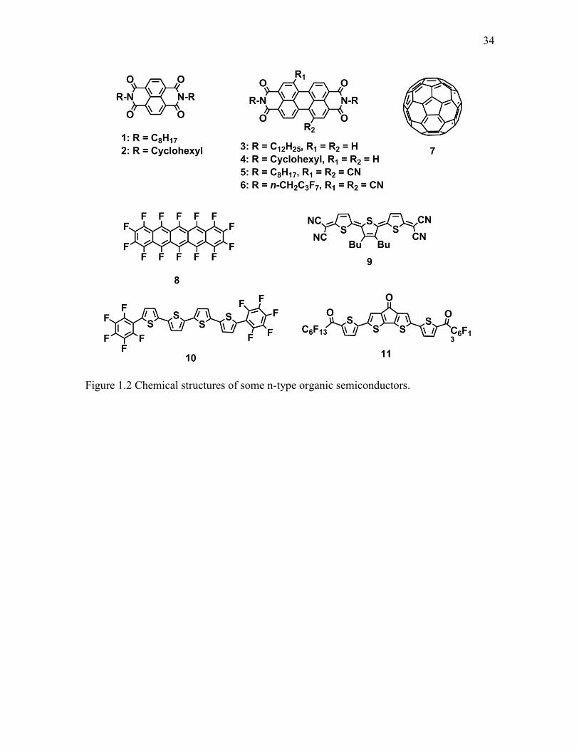
34
Figure 1.2 Chemical structures of some n-type organic semiconductors.

35
Figure 1.3 Schematic of doping mechanism in organic semiconductors.

36
Figure 1.4 Schematic demonstrations of energy levels and the corresponding density of
states of p- and n-doping in the case of IPA and the formation of CTCs with their
subsequent ionization. Adapted from ref 38, published 2016 by the ACS Publications.

37
Figure 1.5 A prototype charge-transfer compound TTF-TCNQ: (a) schematic illustration
of formation of TTF-TCNQ charge transfer complex; (b) arrangement of the TTF and
TCNQ molecules in a crystal. Adapted from ref 72, published 2008 by the Nature
Publishing Group.

38
Figure 1.6 The ideal structure of a BHJ organic solar cell. Adapted from ref 10, published
2007 by the ACS Publications.

39
Figure 1.7 Chemical structure of a PTCDI molecule.

40
Figure 1.8 The frontier orbitals of the highest occupied molecular orbital (HOMO) (top)
and lowest unoccupied molecular orbital (LUMO) (bottom) of PTCDI. Adapted from ref
86, published 2004 by The Royal Society of Chemistry.

41
Figure 1.9 Molecular and crystal structure of PTCDIs: (a) the PTCDI-C8 unit cell as
gained by single-crystal X-ray diffraction; (b) the theoretically predicated PTCDI-C8
crystal growth direction (adapted from ref 95, published 2007 by the ACS Publications);
(c) the chemical structure of CH-PTCDI; (d) the filp-flap molecular stacking along the
[100] direction (adapted from ref 96, published 2009 by the ACS Publications).

42
Figure 1.10 A schematic diagram showing the electron transport properties in PTCDI
nanofibers with D-A structure.

43
Figure 1.11 Photoinduced electron transfer between donor and acceptor with two possible
processes: (a) electron transfers from excited donor to PTCDI or (b) electron moves from
donor to excited PTCDI molecules.

44
Table 1.1 Calculated diffusion lengths (LD) for singlet (S) and triplet (T) excitons of
crystalline (C.) and amorphous (Amorph.) films (adapted from refer 81, published 2009
by the AIP Publishing).
Material
Exciton
Crystallinity (Orientation)
LD
(nm)
NPD S Amorph. 5.1 (±1.0)
CBP S Amorph. 16.8 (±0.8)
SubPc S Amorph. 8.0 (±0.3)
PTCDA S C.-55 nm (flat) 10.4 (±1.0)
DIP S C.- > 150 nm (upright) 16.5 (±0.4)
DIP S C.-30 nm (flat) 21.8 (±0.6)
PtOEP T-Mon. C.- > 150 nm (upright) 18.0 (±0.6)
PtOEP T-Dim. C. - > 150 nm (upright) 13.1 (±0.5)

CHAPTER 2
CHEMICAL SELF-DOPING OF ORGANIC NANORIBBONS
FOR HIGH CONDUCTIVITY AND POTENTIAL
APPLICATION AS CHEMIRESISTIVE SENSOR1
2.1 Abstract
Intrinsically low electrical conductivity of organic semiconductors hinders their
further development into practical electronic devices. Herein, we report on an efficient
chemical self-doping to increase the conductivity through one-dimensional (1D) stacking
arrangement of electron donor-acceptor (D-A) molecules. The D-A molecule employed
was a 1-methylpiperidine-substituted perylene tetracarboxylic diimide (MP-PTCDI), of
which the methylpiperidine moiety is a strong electron donor, and can form a charge
transfer complex with PTCDI (acting as the acceptor), generating anionic radical of
PTCDI as evidenced in molecular solutions. Upon self-assembling into nanoribbons
through columnar stacking, the intermolecular charge transfer interaction between
methylpiperidine and PTCDI would be enhanced, and the electrons generated are
1 Reprinted with permission from Wu, N.; Wang, C.; Bunes, B. R.; Zhang, Y.; Slattum, P.
M.; Yang, X.; Zang, L., Chemical Self-doping of Organic Nanoribbons for High
Conductivity and Potential Application as Chemiresistive Sensor. ACS Appl. Mater.
Interfaces 2016, 8, 12360-12368. Copyright (2016) American Chemical Society.
46
delocalized along the stacking of PTCDIs, leading to enhancement in conductivity.
The conductive fiber materials thus produced can potentially be used as chemiresistive
sensor for vapor detection of electron deficient chemicals such as hydrogen peroxide,
taking advantage of the large surface area of nanofibers. As a major component of
improvised explosives, hydrogen peroxide remains a critical signature chemical for
public safety screening and monitoring.
2.2 Introduction
Organic semiconductors are an alternative to conventional inorganic semiconductors,
and offer advantages such as mechanical flexibility and ease of solution processing. They
have been applied in varying electronic devices, including organic field-effect transistors
(OFETs),1 organic light-emitting diodes (OLEDs),2 photovoltaics,3 photodetectors,4 and
sensors.5,6 Unfortunately, their intrinsically low electrical conductivity,7 due to properties
such as the closed-shell electronic structures of the individual organic molecules and
weak intermolecular interactions, hinders further development and more widespread
applications. Studies have shown that electrical doping of organic semiconductors is an
effective strategy to overcome this limitation,8 enhancing conductivity by many orders of
magnitude. Doping requires matched energy levels (redox potentials) between the host
molecules and dopants.8 Hence, the number of dopants is limited. Common dopants are
small molecules like O2,9 Br2, I2,
10 and larger molecules, such as F4-TCNQ
(perfluorinated tetracyanoquinodimethane),11 and pyronin B.12 Nevertheless, all of these
are interstitial dopants which are mobile in the host materials,8 so the electrical properties
of the doped organic semiconductors may change in time as the dopants diffuse.

47
Therefore, exploration of a new type of dopant is important for achieving high quality
organic semiconductor materials.
Substitutional n-type doping was previously achieved by introducing a zwitterionic
dopant to the perylene tetracarboxylic diimide (PTCDI) molecules.13-15 The dopant was a
reduced species (anionic radical) of the host molecule, so they did not significantly alter
the crystal structure and were fixed in the semiconductor lattice. The conductivity was
dependent on the concentration of dopant and showed large enhancement even with small
amount of dopants. Anionic radicals of PTCDI molecules can also be generated by
interacting with reducing agent like hydrazine.16 After exposure to hydrazine vapor, the
nanobelts self-assembled from PTCDIs increased conductivity because of the formation
of PTCDI anionic radicals, which provide electrons as the major charge carrier rapidly
migrating along the long axis of nanobelt through delocalization. With the similar
process and mechanism, OFETs based on hydrazine doped PTCDI molecules were
fabricated to achieve lower operating voltages and higher conductivity.17
Inspired by these works, we designed PTCDI molecules substituted with 1-
methylpiperidine (MP) to construct self-doped semiconductor through one-dimensional
(1D) self-assembly of the molecules into nanoribbons structure. The methylpiperidine
moiety on one molecule, a strong electron donor (D), interacted with PTCDI on the other
molecule (acting as the electron acceptor, A), generating anionic radicals of PTCDI. The
resultant radicals functioned as the n-type dopants located in the lattice of the PTCDI
semiconductors.13-15 The similar side-group induced self-doping has also been widely
exploited in conducting polymer materials, e.g., polyaniline.18,19 The nanoribbon
structure, dominated by the stacking between the PTCDI planes, provides an

48
efficient pathway for long-range charge transport.20 The nanoribbons reported in this
study exhibited four orders of magnitude higher current compared to the 1D
nanomaterials assembled from other PTCDI molecules under the same test conditions.21
With high conductivity, the n-type PTCDI nanoribbons can potentially be developed
as a chemiresistive sensor for detection of electron deficient chemicals with a high signal-
to-noise ratio, providing more reliable output signal and lower limit of detection. As
indeed evidenced in this study, the PTCDI nanoribbons demonstrate sensitive
chemiresistive response to the hydrogen peroxide (H2O2) vapor, enabling potential
application in detection of improvised explosives, such as triacetone triperoxide (TATP),
diacetone diperoxide (DADP), hexamethylene triperoxide diamine (HMTD), and simple
liquid mixtures of concentrated hydrogen peroxide and fuels (e.g., alcohols, acetone).22
H2O2 is commonly used as the chemical marker of these peroxide explosives. Current
techniques for detecting H2O2 are fluorometric,22-24 colorimetric,25 and electrochemical
methods,26 but most of them are limited to detection in the liquid phase. It is still
challenging to detect H2O2 vapor at trace level. The chemiresistive sensing technique has
the advantages of trace vapor detection and enables fabricating a portable, low-power and
simple sensor device.27,28
2.3 Experimental Section
2.3.1 Synthesis of N-dodecyl-N’-[(1-methylpiperidine-4-yl)
methyl]-perylene-3,4,9,10-tetracarboxylic Diimide
The precursor compound, N-dodecyl-perylene-3,4,9,10-tetracarboxylic monoimide
monoanhydride (Compound 1, Figure 2.1), was synthesized using a previous method.21

49
Subsequently, Compound 1 (100 mg), (1-methyl-4-piperidinyl)methanamine (Sigma-
Aldrich, 71.3 mg), zinc acetate (Sigma-Aldrich, ACS reagent, 98, 3.0 mg) and
imidazole (Sigma-Aldrich, ACS reagent, 99, 1.5 g) were combined and heated to 150
C for 8 hours. After cooling to room temperature, the reaction mixture was dispersed in
10 HCl (Fisher Chemical, 36.5 to 38.0, ww) solution to solubilize the imidazole, the
insoluble product was collected by filtration and washed with water and methanol. The
crude product was converted to the free base by dissolving in chloroform and washing
with 10 NaOH (Sigma-Aldrich, ACS reagent, 97.0) solution. The organic layer was
washed with water and dried over anhydrous Na2SO4 (Sigma-Aldrich, ACS reagent,
99). The reaction mixture was then purified by silica gel chromatography using 6.0
ethanol in chloroform as the eluent followed by recrystallization from chloroformethanol
to give final product (54.7 mg, 46). 1H NMR (500 MHz, CDCl3, TMS, ppm): δ 8.65
(d, J 8.0 Hz, 4H; perylene H), 8.57 (d, J = 8.0 Hz, 4H; perylene H), 4.214.14 (m, 4H;
(CO)2NCH2), 2.87 (m, 2H; CHH*N(CH3)CHH*), 2.26 (s, 3H; NCH3), 1.961.88 (m, 2H;
CH*HN(CH3)CH*H), 1.791.71 (m, 4H; (CH2*)2CHCH2N), 1.341.22 (m, 21H,10CH2,
CH), 0.87 (t, J 6.84 Hz, 3H; CH3); 13C NMR (125 MHz, CDCl3, TMS, ppm): δ
173.26, 163.88, 163.53, 137.05, 134.87, 134.70, 131.72, 131.56, 129.62, 129.54, 126.62,
123.60, 123.39, 123.32, 123.26, 116.49, 115.30, 55.65, 46.52, 40.95, 32.13, 30.46, 29.91,
29.84, 29.77, 29.60, 29.56, 28.34, 27.39, 22.89, 14.31. MALDI-TOF-MS: [MH]z
670.35.

50
2.3.2 Fabrication of Nanoribbons
Self-assembly of the MP-PTCDI molecules was performed through a solvent
exchange process from a “good” solvent to a “bad” solvent, where the molecules have
limited solubility in the “bad” solvent and thus self-assemble into one-dimensional
nanostructures via molecular stacking.21 In this study, we used a solution injection
method to conduct the self-assembly in ethanol. Typically, 0.4 mL of MP-PTCDI
solution (1.5 mmolL1) in chloroform was injected rapidly into a larger volume of
ethanol (4 mL) and placed in the dark for 5 h. The nanoribbons were then transferred to
substrates for further characterization and electrical measurements. Synthesis of MA-
PTCDI and MO-PTCDI, and self-assembly into nanoribbons were performed according
to the previously reported methods.21 Synthesis of CH-PTCDI molecules and self-
assembly into nanobelts were based on the previously reported methods.29
2.3.3 Materials Characterization
UV-Vis absorption spectra were collected with an Agilent Cary 100. Fluorescence
spectra were acquired on an Agilent Eclipse spectrophotometer. AFM measurements
were carried out on a Veeco MultiMode V scanning probe microscope in tapping mode.
SEM measurement was performed with an FEI Nova Nano 630 (FEI Corporation) with a
helix detector in low vacuum (0.43 Torr water pressure). To make samples for either
AFM or SEM measurements, the MP-PTCDI nanoribbons were directly transferred from
ethanol and deposited onto a silicon substrate coated with a polished 300 nm thick SiO2
layer, and then dried in vacuum oven at room temperature in the dark. The bright field
and fluorescence optical images were obtained with a Leica DMI4000B inverted

51
microscope equipped with an Acton SP-2356 Imaging Spectrograph system and
Princeton Instrument Acton PIXIS: 400B Digital CCD Camera System for high
resolution imaging
2.3.4 Current Measurement
Interdigitated electrodes (IDE) were used for all current measurements in this work.
The IDE has a channel width of 2100 μm and a gap length of 50 μm, and was fabricated
by a standard photolithography procedure on a silicon wafer with a 300 nm thermal oxide
layer (Silicon Quest International). The electrodes were made by sputtering with 20 nm
titanium adhesion layer and 50 nm gold layer. MP-PTCDI nanoribbons were deposited
onto IDE by drop-casting, followed by drying in vacuum oven at room temperature in the
dark. The electrical conductivity was measured under ambient conditions using a two-
probe method on a Signatone S-1160 Probe Station combined with an Agilent 4156C
Precision Semiconductor Analyzer. To compare the conductivity of different PTCDI
nanomaterials, the nanofibers were assembled by injecting a given molar amount of
PTCDI (12 nmol dissolved in a minimal volume of CHCl3) into 100 μL ethanol. The
nanofibers thus assembled were dispersed well in ethanol, which were then transferred
onto the IDE by slow drop-casting to ensure uniform coverage over the whole IDE area.
To compare the current enhancement ratio after surface coating with amines, 12 nmol of
CH-PTCDI nanobelts were chosen as the standard, zero-doping material, and deposited
onto the IDE. 1 μL of methanol solution containing different concentrations of the amines
(1-methylpiperidine, TCI America, 99.0; hexylamine, Acros Organics, 99;
triethylamine, Sigma-Aldrich, 99; aniline, Acros Organics, 99.5, extra pure) were

52
drop cast onto the surface of the CH-PTCDI nanobelts, providing the varying molar
amount of amine coated on the surface. To avoid the oxidation of amines during
processing, the fresh amine solution was made for each measurement. 1H NMR
measurements were conducted for all the amines during the project period to assure that
the high purity of amines remained throughout the experiments. 1-Methylpiperidine: 1H
NMR (300 MHz, CDCl3, TMS, ppm): δ 2.26 (m, 4H, CH2CH2*N), δ 2.17 (s, 3H,
NCH3), δ 1.52 (m, 4H, CH2CH2*CH2), δ 1.35 (m, 2H, CH2CH2*CH2). Hexylamine:
1H NMR (300 MHz, CDCl3, TMS, ppm): δ 2.64 (t, J 6.0 Hz, 2H, NH2), δ 1.401.17
(m, 10H, (CH2)5), δ 0.85 (t, J 6.0 Hz, 3H, CH3). Triethylamine: 1H NMR (300 MHz,
CDCl3, TMS, ppm): δ 2.49 (q, J = 6.0 Hz, 6H, CH2), δ 0.99 (t, J 6.0 Hz, 9H, CH3).
Aniline: 1H NMR (300 MHz, CDCl3, TMS, ppm): δ 7.20 (t, J 6.0 Hz, 2H,
CHCH*CH), δ 6.80 (t, J 6.0 Hz, 1H, CHCH*CH), δ 6.72 (d, J 6.0 Hz, 2H,
CCH*CH), δ 3.65 (s, 2H, NH2).
2.3.5 Chemical Vapor Sensing Measurement
All chemical vapor sensing tests were conducted under ambient conditions in the
dark. Figure 2.2 depicts the sensing and chemical vapor delivery systems. A certain
amount of chemical vapor was pulled into a 50 mL syringe and delivered by syringe
pump (NE-4000 New Era Pump System, Inc.) at a rate of 25 mLmin1 into the carrier
gas. The carrier gas was dry air with a flow rate of 475 mLmin1. The final concentration
of chemical vapor in the testing chamber was calculated from the syringe volume and the
concentration of original chemical vapor. The original H2O2 vapor was generated from
44.7 wt. H2O2 solution (Sigma-Aldrich, 50 wt. in H2O).30 The IDE chip (deposited

53
with PTCDI nanomaterials) was placed on a ceramic chip carrier connected by wire
bonding. The ceramic chip carrier was fixed on a breadboard, enclosed in a small Teflon
chamber (3.84 cm in length, 1.86 cm in width, and 2.41 cm in height), and connected to
an Agilent 4156C Semiconductor Analyzer. A bias of 10 V was applied across the
electrodes and the current through the sensor was monitored. For H2O2 testing, the chip
was exposed to H2O2 vapor for 30 s with a recovery time of 2.5 min. For testing toward
the common liquid samples, the exposure time was 30 s with a recovery time of 30 s. The
sensing response time of MP-PTCDI nanoribbons was obtained by fitting the time-course
current change profile to an exponential function,31 which gives the response time as 1e
of the time constant obtained.
2.4 Results and Discussion
2.4.1 Synthesis of MP-PTCDI Molecules and
Self-Assembly Into Nanoribbons
PTCDI-based molecules have been extensively explored for 1D self-assembly and
optoelectronic applications in recent years.20,32-35 Side-chain substitutions do not
significantly influence the electronic property of the PTCDI backbone because the two
imide positions in the PTCDI molecules are nodes in the -orbitals.32,36 This allows for
comparative study of the PTCDI materials, for which the side-chain substitutions play an
important role in intermolecular interactions, resulting in different electronic properties
through charge transfer.37 In this study, a PTCDI molecule substituted with 1-
methylpiperidine moiety (Figure 2.3, denoted as MP-PTCDI) was designed and
synthesized. The MP-PTCDI nanoribbons were fabricated using the previously reported
54
solution phase self-assembly method.20,21,35 The morphology of MP-PTCDI nanoribbons
was characterized by SEM and AFM (Figure 2.4). The nanoribbons are several
micrometers in length and 100300 nm in width. The thickness of the nanoribbons is
estimated to be just about 15 nm (Figure 2.4b, AFM images and height-profile). Such
shape-defined 1D nanoribbon structures are conducive to the construction of electronic
devices. For comparative study, two other PTCDI molecules, MA-PTCDI and MO-
PTCDI (both substituted with the same dodecyl alkyl chain, but with different groups on
the other end, as shown in Figure 2.3), were also synthesized and assembled into
nanoribbon structures following the previous reported methods.21 Owing to the similar
molecular structure, the two reference PTCDIs formed about the same nanoribbon
morphology as the MP-PTCDI (see Table 2.1). The dimethylaniline moiety of MA-
PTCDI acts as a strong electron donor under photoexcitation, whereas the methoxyphenyl
is not an effective donor to PTCDI as evidenced from our previous investigation.21 In the
next section, we compared the electrical conductivity of the nanoribbons assembled from
the three PTCDI building blocks shown in Figure 2.3, aiming to explore the effects of the
side groups on self-doping.
2.4.2 High Conductivity and Mechanism Study
As shown in Figure 2.5, MP-PTCDI nanoribbons possess the highest electrical
conductivity; the current of the MP-PTCDI nanoribbons is four orders of magnitude
higher than the other PTCDI nanoribbon materials under the same test conditions.
Considering the similar nanoribbon structures formed from the three PTCDIs (Table 2.1)
and the fact that the -electronic property of PTCDI backbone remains unchanged with

55
different side-substitutions, we concluded that the high conductivity observed for MP-
PTCDI nanoribbons is largely caused by the methylpiperidine moiety.19
To gain insight into the high conductivity of MP-PTCDI nanoribbons, a case study
model was constructed by coating 1-methylpiperidine molecules on N,N-di(cyclohexyl)-
perylene-3,4,9,10-tetracarboxylic diimide (CH-PTCDI) nanobelts to investigate the
influence of this specific substitution group on the conductivity of one-dimensional
PTCDI nanomaterials.38,39 The CH-PTCDI was selected because the cyclohexyl side-
chain groups are neutral and inactive in charge transfer interaction, and the shape defined
nanobelts can be easily fabricated from this molecule with high reproducibility.29 In this
study, 12 nmol of CH-PTCDI nanobelts were deposited onto interdigitated electrodes
(IDEs) patterned on a silicon wafer, and a controlled amount of 1-methylpiperidine was
drop-cast onto the nanobelts (Figure 2.6a). Negligible currents were measured for either
pristine CH-PTCDI nanobelts (0.0012 nA at a bias of 10 V, Figure 2.7) or pure 1-
methylpiperidine film drop-cast from 4 μmol amount (0.0055 nA at a bias of 10 V,
Figure 2.7). In contrast, a much increased current was observed for the CH-PTCDI
nanobelts coated with only 2 mol of 1-methylpiperidine (0.45 nA at a bias of 10 V,
Figure 2.7). The current increased further when more 1-methylpiperidine was deposited.
The current increased to 32.5 μA, an enhancement ratio of 2×10⁷ compared to the pristine
nanobelt, when 4 mol of 1-methylpiperidine was deposited (Figure 2.6b). An
enhancement ratio of 8×10⁶ was observed when 8 μmol of 1-methylpiperidine was
deposited, indicating that the current increase started to reach saturation when more than
4 μmol of 1-methylpiperidine was cast (Figure 2.6b). This significant increase in
conductivity is likely due to the chemical doping, which occurs through the donor-

56
acceptor (charge transfer) interaction between 1-methylpiperidine and PTCDI.
The morphology of the CH-PTCDI nanobelts before and after surface coating
remained unchanged as characterized by SEM (Figure 2.6c, d). Interestingly, the built up
surface charging on the pristine CH-PTCDI nanobelts was eliminated by surface coating
with 1-methylpiperidine. The SEM image of pristine CH-PTCDI nanobelts shows bright
imaging contrast on the surface of the nanobelts, which is a characteristic of the surface
charge built up on the nonconductive sample after E-beam exposure during SEM
measurement (Figure 2.6c).40 However, such surface charging was suppressed after
surface coating of the 1-methylpiperidine (Figure 2.6d). This phenomenon is common in
SEM measurement performed on nonconductive samples, for which a thin layer of metal,
such as Au, Pt, or Pd, is typically deposited on the sample surface to facilitate charge
transmission and prevent charge building up.40,41 Since the pure 1-methylpiperidine film
is little conductive (Figure 2.7), the observed conductivity improvement should be due to
the charge transfer interaction between 1-methylpiperidine and CH-PTCDI nanobelts,
consistent with the current enhancement discussed above.
The charge transfer interaction between 1-methylpiperidine and CH-PTCDI was also
confirmed by the fluorescence quenching measurements of PTCDI. MP-PTCDI solution
in chloroform exhibits strong fluorescence emission, comparable to CH-PTCDI
molecules in chloroform (Figure 2.8),29 indicating that there is no intramolecular electron
transfer in the MP-PTCDI molecule. However, no fluorescence emission was observed
for the nanoribbons fabricated from the MP-PTCDI molecules (Figure 2.9ac). By
contrast, the CH-PTCDI nanobelts still have considerable fluorescence emission (Figure
2.9df). The fluorescence quenching within MP-PTCDI nanoribbons is likely caused by

57
the intermolecular electron transfer between 1-methylpiperidine on one molecule and the
PTCDI part on the other molecule. To prove this intermolecular charge transfer,
fluorescence spectra of the reference PTCDI, CH-PTCDI, were measured in chloroform
solutions with and without addition of 1-methylpiperidine (Figure 2.10a). Significant
fluorescence quenching (indicative of charge transfer interaction) was observed with
increasing the concentration of 1-methylpiperidine, which follows the linear Stern-
Volmer relationship (Figure 2.10b). The linear fitting gives the binding constant of 21.6
M1 between 1-methylpiperidine and the PTCDI. The binding constant obtained is about
one order of magnitude higher than those measured for the aromatic hydrocarbon donor-
acceptor complexes reported by others.42 The enhanced binding is largely due to the
stronger electron donating capability of organic amines, compared to the aromatic
hydrocarbons.
To determine whether other amines can interact with PTCDI as strong as 1-
methylpiperidine, aniline, hexylamine, and triethylamine were selected for comparative
testing. Following the same experimental procedure of surface doping as described
above, different amount of amines were drop-cast onto the surface of the CH-PTCDI
nanobelts. As shown in Figure 2.11a, when 0.5 mol of amine was applied, no obvious
current enhancement was obtained by coating with aniline, hexylamine, and
triethylamine, whereas a 26-fold increase in current was observed by coating with 1-
methylpiperidine under the same condition. However, significant increase in current was
observed when the amount of hexylamine and triethylamine increased to 8 μmol, for
which the enhancement ratios were about 3000 and 1800, respectively (though still three
orders of magnitude lower than 1-methylpiperidine), whereas aniline still produced

58
negligible current even with as much as 12 μmol coated (Figure 2.11b).
Regarding the fact that the CH-PTCDI nanobelts coated by the three amines under
study (1-methylpiperidine, hexylamine, and triethylamine) produced enhanced
conductivity relative to the pristine CH-PTCDI nanobelts while those treated with aniline
did not, we further studied the interaction between CH-PTCDI molecules and amines
using UV-vis absorption spectroscopy. Inspired by our previous work,16 in which a strong
electron donor (e.g., hydrazine) reduced PTCDI molecules to anionic radicals, we also
detected the PTCDI anionic radical upon adding the three amines into the oxygen free
solution of CH-PTCDI in dimethyl sulfoxide (DMSO). The existence of three new
absorption peaks at 708, 798, and 959 nm in the presence of 1-methylpiperidine indicates
the formation of PTCDI anionic radicals (Figure 2.12).16,17,43 In the absence of oxygen,
the radicals are very stable. Upon exposure to air, the three characteristic peaks diminish
with time, which further confirms the formation of oxygen-sensitive PTCDI anionic
radicals. Moreover, analysis based on the redox potentials suggests that the electron
transfer from 1-methylpiperidine to PTCDI is a thermodynamic favorable (spontaneous)
process. The Gibbs free energy change (ΔG) of the electron transfer can be calculated
from the redox potentials of species under certain concentrations; ΔG thus obtained will
indicate if the electron transfer is a thermodynamic favorable (spontaneous) process.
The oxidation potential of 1-methylpiperidine (MP) is 1.08 V vs SCE,44 and the
reduction potential of PTCDI is 0.658 V vs SCE45 (Note: the electronic property (redox
potential) of PTCDI does not change significantly with the different side groups since the
two imide positions are node in the -conjugation). The starting concentration of PTCDI
and MP used in Figure 2.12 were 10 μmolL1 and 0.1 molL1, respectively. When the

59
redox reaction reached its equilibrium as shown in Figure 2.12, the concentration of
PTCDI anionic radical can be estimated to be about 1×10⁷ molL, according to Beer-
Lambert law (given the molar absorption coefficient of PTCDI anionic radical is ϵ
36000 M1.cm1 at 956 nm,13 peak absorbance 0.0039 at that wavelength, loptical length
1 cm). The concentration of the counterpart MP should be the same as that of PTCDI
anionic radical, 1×10⁷ molL. So, from the Nernst equation (Equation 2.1), the
electrical potential (ΔE) of the redox (electron transfer) reaction between MP and PTCDI
can be calculated to be 0.042 V, which gives a negative ΔG (Equation 2.2), meaning a
spontaneous process for the electron transfer in the solution phase. This is consistent with
our observation as shown in Figure 2.12
∆𝐸 = ∆𝐸0 −𝑅𝑇
𝑧𝐹𝑙𝑛
[𝑃𝑇𝐶𝐷𝐼−][𝑀𝑃+]
[𝑃𝑇𝐶𝐷𝐼][𝑀𝑃] 𝑇 = 293 𝐾 2.1
∆𝐺 = −𝑛𝐸𝐹 2.2
In addition to 1-methylpiperidine, PTCDI anionic radicals were also generated by
addition of hexylamine and triethylamine (Figure 2.13). However, no such anionic
radicals were generated upon addition of aniline to the same deoxygenated solution of
CH-PTCDI (Figure 2.13). This comparative observation is consistent with the above
discussed results of conductivity enhancement upon casting of different amines,
indicating that the effective charge transfer interaction (and thus generating PTCDI
anionic radical) is the primary cause of the conductivity enhancement. The electrons thus
generated can delocalize (migrate) along the stacking of PTCDIs,20,34,46 acting as the

60
major charge carrier for the n-type material.
The electron donating strength of amines can be evaluated by the oxidation potentials
as others did for evaluating the charge transfer in different donor-acceptor pairs.42 Among
all the amines used in this project, aniline would be the strongest electron donor from
their oxidation potentials (1-methylpiperidine, Eoox 1.08 V vs SCE;44 hexylamine, Eo
ox
1.44 V vs SCE;47 triethylamine, Eoox 0.99 V vs SCE;48 aniline, Eo
ox 0.86 V vs
SCE48). However, as evidenced by our results, no charge transfer was observed between
aniline and PTCDI even in the presence of a large excess of aniline (i.e., no significant
current enhancement was observed with 12 μmol aniline coated on the CH-PTCDI
nanobelts, and no absorption peaks of PTCDI anionic radical were detected in the
deoxygenated DMSO solution of CH-PTCDI (10 μmolL1) in the presence of excessive
aniline (0.1 molL1)). The lack of charge transfer between aniline and PTCDI might be
due to the weak nucleophilicity of aniline,49 which prevents the strong donor-acceptor
interaction.
On the basis of the aforementioned results and discussion, we propose a possible n-
type doping mechanism, which is a result of the generation of PTCDI anionic radicals, to
explain the high conductivity of the MP-PTCDI nanoribbons. As demonstrated in Figure
2.14, upon self-assembly into nanoribbons, the side-groups of 1-methylpiperidine are in
close proximity of the PTCDI backbones, enabling charge transfer interaction to form
PTCDI anionic radicals (the reduction of PTCDI by 1-methylpiperidine should be more
thermodynamically favored in solid state compared to solution phase due to the much
higher local concentration in solid). Owing to the efficient intramolecular -electron
delocalization within the PTCDI plane, the electron (anionic radical) generated can be

61
well stabilized (against charge recombination) as observed in the UV-vis absorption
spectral measurement (Figure 2.12). When this occurs inside the nanoribbons, the
electron can effectively survive from the scavenging by oxygen, making the high
conductivity gained sustainable even in the ambient environment as indeed observed in
this study (Figure 2.5 and Figure 2.6). With an applied bias, the self-doped electrons
rapidly migrate along the long axis of the nanoribbon facilitated by the intermolecular
electron delocalization,16,46,50 leading to the high conductivity. The resultant PTCDI
anionic radical is an n-type dopant and is similar to the ones employed in other works,13-
15 in which the substitutional dopant was a zwitterionic molecule, a PTCDI anionic
radical linked to an amine centered cation (a reduced analogue of the PTCDI host
molecule). An n-doped PTCDI film was fabricated by spin-coating mixed PTCDI dopant
and host materials solution, resulting in ten orders of magnitude of increase in
conductivity with just 1 doping. The doping process reported in this work is also
similar to the self-doped conductor of tetrathiafulvalene (TTF) derivative.51 TTFCOOH is
an insulator, but upon reaction with NH3, it switches into a conductor TTFCOONH4
with a conductivity of 2×10⁴ Scm1. It was demonstrated that the conductivity gained in
the salt came from a radical species TTF•COONH4 generated by self-protonation of
the TTF moiety.
2.4.3 Chemiresistive Sensing for Hydrogen Peroxide Vapor Detection
With the increased electrical conductivity by self-doping, MP-PTCDI nanoribbons
can be a potential building material for chemiresistive sensors, for which the high
conductivity improves the signal-to-noise ratio and simplifies the system design. A

62
chemiresistive sensor based on the nanoribbons benefits from the large surface area and
continuous porosity formed by the interlaced nanoribbons deposited on the substrate.
Combination of these two features enhances the adsorption and diffusion (accumulation)
of gas analytes, thus increasing the sensitivity to the analytes. The n-type character of the
PTCDI material allows for chemiresistive sensing of electron deficient analytes, which
can be bound to the surface, causing charge depletion of the material. In this study we
chosen H2O2 vapor as the target analyte because it is a critical signature for the peroxide
explosives including both the synthetic ones (e.g., TATP, DADP and HMTD) and the
simple liquid mixtures of H2O2 and the fuels.22
Figure 2.15 shows the real-time electrical current profile of a MP-PTCDI nanoribbon
chemiresistor sensor in response to H2O2 vapor. Upon exposure to H2O2 vapor (18.5
ppm), there is an instantaneous decrease in current of about 50 (Figure 2.16
demonstrates how to calculate the current decrease of MP-PTCDI nanoribbons in
response to H2O2 vapor). A very short response time of 19.5 s is attributed to the large
surface area of nanoribbons and expedient diffusion of H2O2 vapor. The response is
concentration dependent. Figure 2.15b shows a plot of relative sensor response as a
function of the concentration of H2O2 vapor, which can be fit well into the Langmuir
absorption model (Equation 2.3).5
𝐼0 − 𝐼
𝐼0=
𝑐 ∙ 𝑘 ∙ [𝐻2𝑂2]
1 + 𝑘 ∙ [𝐻2𝑂2] 2.3
where c is a proportional constant; k is a static equilibrium constant; [H2O2] is the vapor
concentration of H2O2. Fitting the date in Figure 2.15b gives c = 67.42, k = 0.15, with a

63
R2 = 0.9512. The lowest concentration of H2O2 vapor that was tested in this study was 0.6
ppm, which represents the lowest level that can be provided by the present experimental
setup.52 This level of H2O2 vapor represents two orders of magnitude dilution of the
saturated vapor of commercial 50 wt% H2O2 solution. The irreversible sensor response
towards H2O2 is attributed to the strong surface binding of H2O2 and the permanent
oxidation of 1-methylpiperidine groups by H2O2 (Eored 1.78 V, vs SCE).53
In addition to the high sensitivity, the MP-PTCDI nanoribbons also demonstrated
high selectivity towards H2O2 vapor against water and the common organic liquids,
facilitating the development into practical sensing applications. Such general selectivity
was investigated by measuring the sensor response toward the vapor of various common
liquids, including water, acetone, ethyl acetate, dichloromethane, methanol, ethanol,
toluene, and hexane. In contrast to the irreversible decrease response caused by H2O2
vapor, exposure to these liquids vapor resulted in reversible increase in current for the
MP-PTCDI nanoribbons (Figure 2.17). The increased conductivity observed is likely a
result of dipole interaction between MP-PTCDI nanoribbon and the liquid molecule.54,55
Table 2.2 lists the dipole moments of all the liquid analytes tested56 and the
corresponding sensor responses measured at 5 of the saturated vapor concentration.
Clearly, the sensing response and the dipole moment of the liquids are tightly correlated.
For liquids with smaller dipole moments, the response is lower. For example, the vapor
concentration of hexane used (8400 ppm) is much higher than many other analytes, such
as ethyl acetate (4900 ppm), water (1100 ppm), ethanol (3000 ppm), toluene (1500 ppm),
but the relative response is only 0.1, the lowest among all chemicals studied here,
because the dipole moment of hexane is less than 0.1 Debye, much lower than others.

64
2.5 Conclusions
In conclusion, the nanoribbons assembled from the 1-methylpiperidine substituted-
PTCDI molecules possess extraordinarily high conductivity relative to other PTCDI-
based nanostructures. The 1-methylpiperidine group plays a key role in the conductivity
enhancement, as evidenced by systematic experiments and analysis of the interaction
between a model PTCDI nanobelt and 1-methylpiperidine. Upon self-assembly into one-
dimensional nanoribbons, the 1-methylpiperidine groups interact with the PTCDI core in
stacking proximity to produce the PTCDI anionic radical, which acts as the n-type dopant
in the PTCDI lattice. The doping process increases the charge carrier density within the
PTCDI nanoribbons, and the one-dimensional stacking of PTCDIs is efficient for
long range charge migration, thereby resulting in high conductivity. The high
conductivity obtained enables application in chemiresistive sensors. The PTCDI
nanoribbons demonstrated highly sensitive response to H2O2 vapor through oxidation,
rather than dipole moment interaction as in the case of common liquid vapor, thereby
producing general selectivity toward H2O2 vapor. Owing to the high conductivity of MP-
PTCDI nanoribbons, as well as the porous mesh-like morphology of the nanoribbon film,
the lowest detected concentration of H2O2 vapor in this study was down to 0.6 ppm. This
work provides an alternative approach to fabricating self-doped organic semiconductors
with high conductivity by molecular engineering.
2.6 References
(1) Allard, S.; Forster, M.; Souharce, B.; Thiem, H.; Scherf, U. Organic Semiconductors
for Solution-Processable Field-Effect Transistors (OFETs). Angew. Chem., Int. Ed. 2008,
47, 4070-4098.

65
(2) Gross, M.; Muller, D. C.; Nothofer, H.-G.; Scherf, U.; Neher, D.; Brauchle, C.;
Meerholz, K. Improving the Performance of Doped π-Conjugated Polymers for Use in
Organic Light-Emitting Diodes. Nature 2000, 405, 661-665.
(3) Hains, A. W.; Liang, Z.; Woodhouse, M. A.; Gregg, B. A. Molecular
Semiconductors in Organic Photovoltaic Cells. Chem. Rev. 2010, 110, 6689-6735.
(4) Baeg, K.-J.; Binda, M.; Natali, D.; Caironi, M.; Noh, Y.-Y. Organic Light Detectors:
Photodiodes and Phototransistors. Adv. Mater. 2013, 25, 4267-4295.
(5) Huang, H.; Gross, D. E.; Yang, X.; Moore, J. S.; Zang, L. One-Step Surface Doping
of Organic Nanofibers to Achieve High Dark Conductivity and Chemiresistor Sensing of
Amines. ACS Appl. Mater. Interfaces 2013, 5, 7704-7708.
(6) Medina-Sánchez, M.; Martínez-Domingo, C.; Ramon, E.; Merkoçi, A. An Inkjet-
Printed Field-Effect Transistor for Label-Free Biosensing. Adv. Funct. Mater. 2014, 24,
6291-6302.
(7) Chan, C. K.; Kim, E. G.; Brédas, J. L.; Kahn, A. Molecular n-Type Doping of
1,4,5,8-Naphthalene Tetracarboxylic Dianhydride by Pyronin B Studied Using Direct and
Inverse Photoelectron Spectroscopies. Adv. Funct. Mater. 2006, 16, 831-837.
(8) Walzer, K.; Maennig, B.; Pfeiffer, M.; Leo, K. Highly Efficient Organic Devices
Based on Electrically Doped Transport Layers. Chem. Rev. 2007, 107, 1233-1271.
(9) Lu, C.-K.; Meng, H.-F. Hole Doping by Molecular Oxygen in Organic
Semiconductors: Band-Structure Calculations. Phys. Rev. B: Condens. Matter Mater.
Phys. 2007, 75, 235206.
(10) Yamamoto, Y.; Yoshino, K.; Inuishi, Y. Electrical Properties of Phthalocyanine-
Halogen Complexes. J. Phys. Soc. Jpn. 1979, 47, 1887-1891.
(11) Maennig, B.; Pfeiffer, M.; Nollau, A.; Zhou, X.; Leo, K.; Simon, P. Controlled p-
Type Doping of Polycrystalline and Amorphous Organic Layers: Self-Consistent
Description of Conductivity and Field-Effect Mobility by a Microscopic Percolation
Model. Phys. Rev. B: Condens. Matter Mater. Phys. 2001, 64, 195208.
(12) Werner, A. G.; Li, F.; Harada, K.; Pfeiffer, M.; Fritz, T.; Leo, K. Pyronin B as a
Donor for n-Type Doping of Organic Thin Films. Appl. Phys. Lett. 2003, 82, 4495-4497.
(13) Gregg, B. A.; Cormier, R. A. Doping Molecular Semiconductors: n-Type Doping
of a Liquid Crystal Perylene Diimide. J. Am. Chem. Soc. 2001, 123, 7959-7960.
(14) Chen, S.-G.; Branz, H. M.; Eaton, S. S.; Taylor, P. C.; Cormier, R. A.; Gregg, B. A.
Substitutional n-Type Doping of an Organic Semiconductor Investigated by Electron
Paramagnetic Resonance Spectroscopy. J. Phys. Chem. B 2004, 108, 17329-17336.
(15) Gregg, B. A.; Chen, S.-G.; Cormier, R. A. Coulomb Forces and Doping in Organic

66
Semiconductors. Chem. Mater. 2004, 16, 4586-4599.
(16) Che, Y.; Datar, A.; Yang, X.; Naddo, T.; Zhao, J.; Zang, L. Enhancing One-
Dimensional Charge Transport through Intermolecular π-Electron Delocalization:
Conductivity Improvement for Organic Nanobelts. J. Am. Chem. Soc. 2007, 129, 6354-
6355.
(17) Arulkashmir, A.; Jain, B.; John, J. C.; Roy, K.; Krishnamoorthy, K. Chemically
Doped Perylene Diimide Lamellae Based Field Effect Transistor With Low Operating
Voltage and High Charge Carrier Mobility. Chem. Commun. 2014, 50, 326-328.
(18) Malinauskas, A. Self-Doped Polyanilines. J. Power Sources 2004, 126, 214-220.
(19) Yue, J.; Epstein, A. J. Synthesis of Self-Doped Conducting Polyaniline. J. Am.
Chem. Soc. 1990, 112, 2800-2801.
(20) Zang, L.; Che, Y.; Moore, J. S. One-Dimensional Self-Assembly of Planar π-
Conjugated Molecules: Adaptable Building Blocks for Organic Nanodevices. Acc. Chem.
Res. 2008, 41, 1596-1608.
(21) Che, Y.; Yang, X.; Liu, G.; Yu, C.; Ji, H.; Zuo, J.; Zhao, J.; Zang, L. Ultrathin n-
Type Organic Nanoribbons With High Photoconductivity and Application in
Optoelectronic Vapor Sensing of Explosives. J. Am. Chem. Soc. 2010, 132, 5743-5750.
(22) Xu, M.; Han, J.-M.; Wang, C.; Yang, X.; Pei, J.; Zang, L. Fluorescence Ratiometric
Sensor for Trace Vapor Detection of Hydrogen Peroxide. ACS Appl. Mater. Interfaces
2014, 6, 8708-8714.
(23) Xu, M.; Han, J.-M.; Zhang, Y.; Yang, X.; Zang, L. A Selective Fluorescence Turn-
On Sensor for Trace Vapor Detection of Hydrogen Peroxide. Chem. Commun. 2013, 49,
11779-11781.
(24) Abo, M.; Urano, Y.; Hanaoka, K.; Terai, T.; Komatsu, T.; Nagano, T. Development
of a Highly Sensitive Fluorescence Probe for Hydrogen Peroxide. J. Am. Chem. Soc.
2011, 133, 10629-10637.
(25) Xu, M.; Bunes, B. R.; Zang, L. Paper-Based Vapor Detection of Hydrogen
Peroxide: Colorimetric Sensing With Tunable Interface. ACS Appl. Mater. Interfaces
2011, 3, 642-647.
(26) Bai, J.; Jiang, X. A Facile One-Pot Synthesis of Copper Sulfide-Decorated Reduced
Graphene Oxide Composites for Enhanced Detecting of H2O2 in Biological
Environments. Anal. Chem. 2013, 85, 8095-8101.
(27) Guo, P.; Zhao, G.; Chen, P.; Lei, B.; Jiang, L.; Zhang, H.; Hu, W.; Liu, M.
Porphyrin Nanoassemblies via Surfactant-Assisted Assembly and Single Nanofiber
Nanoelectronic Sensors for High-Performance H2O2 Vapor Sensing. ACS Nano 2014, 8,
3402-3411.

67
(28) Bohrer, F. I.; Colesniuc, C. N.; Park, J.; Schuller, I. K.; Kummel, A. C.; Trogler, W.
C. Selective Detection of Vapor Phase Hydrogen Peroxide With Phthalocyanine
Chemiresistors. J. Am. Chem. Soc. 2008, 130, 3712-3713.
(29) Che, Y.; Yang, X.; Balakrishnan, K.; Zuo, J.; Zang, L. Highly Polarized and Self-
Waveguided Emission From Single-Crystalline Organic Nanobelts. Chem. Mater. 2009,
21, 2930-2934.
(30) Manatt, S. L.; Manatt, M. R. R. On the Analyses of Mixture Vapor Pressure Data:
The Hydrogen Peroxide/Water System and Its Excess Thermodynamic Functions. Chem.-
Eur. J. 2006, 12, 3695-3695.
(31) Wang, D.; Chen, A.; Jang, S.-H.; Davies, J.; Jen, A. K. Y. The Effect of Dipole
Moment and Electron Deficiency of Analytes on the Chemiresistive Response of TiO2(B)
Nanowires. Analyst 2011, 136, 4179-4182.
(32) Wurthner, F. Perylene Bisimide Dyes as Versatile Building Blocks for Functional
Supramolecular Architectures. Chem. Commun. 2004, 1564-1579.
(33) Görl, D.; Zhang, X.; Würthner, F. Molecular Assemblies of Perylene Bisimide Dyes
in Water. Angew. Chem., Int. Ed. 2012, 51, 6328-6348.
(34) Zang, L. Interfacial Donor–Acceptor Engineering of Nanofiber Materials to
Achieve Photoconductivity and Applications. Acc. Chem. Res. 2015, 48, 2705-2714.
(35) Chen, S.; Slattum, P.; Wang, C.; Zang, L. Self-Assembly of Perylene Imide
Molecules into 1D Nanostructures: Methods, Morphologies, and Applications. Chem.
Rev. 2015, 115, 11967-11998.
(36) Kazmaier, P. M.; Hoffmann, R. A Theoretical Study of Crystallochromy. Quantum
Interference Effects in the Spectra of Perylene Pigments. J. Am. Chem. Soc. 1994, 116,
9684-9691.
(37) Lei, T.; Luo, J.; Wang, L.; Ma, Y.; Wang, J.; Cao, Y.; Pei, J. Highly Stable Blue
Light-Emitting Materials With a Three-Dimensional Architecture: Improvement of
Charge Injection and Electroluminescence Performance. New J. Chem. 2010, 34, 699-
707.
(38) Che, Y.; Huang, H.; Xu, M.; Zhang, C.; Bunes, B. R.; Yang, X.; Zang, L. Interfacial
Engineering of Organic Nanofibril Heterojunctions into Highly Photoconductive
Materials. J. Am. Chem. Soc. 2011, 133, 1087-1091.
(39) Huang, H.; Chou, C.-E.; Che, Y.; Li, L.; Wang, C.; Yang, X.; Peng, Z.; Zang, L.
Morphology Control of Nanofibril Donor–Acceptor Heterojunction to Achieve High
Photoconductivity: Exploration of New Molecular Design Rule. J. Am. Chem. Soc. 2013,
135, 16490-16496.
(40) Cazaux, J. About the Mechanisms of Charging in EPMA, SEM, and ESEM With

68
Their Time Evolution. Microsc. Microanal. 2004, 10, 670-684.
(41) Moncrieff, D. A.; Robinson, V. N. E.; Harris, L. B. Charge Neutralisation of
Insulating Surfaces in the SEM by Gas Ionisation. J. Phys. D: Appl. Phys. 1978, 11,
2315.
(42) Rathore, R.; Lindeman, S. V.; Kochi, J. K. Charge-Transfer Probes for Molecular
Recognition via Steric Hindrance in Donor-Acceptor Pairs. J. Am. Chem. Soc. 1997, 119,
9393-9404.
(43) Ghosh, I.; Ghosh, T.; Bardagi, J. I.; König, B. Reduction of Aryl Halides by
Consecutive Visible Light-Induced Electron Transfer Processes. Science 2014, 346, 725-
728.
(44) Jakubiak, J.; Allonas, X.; Fouassier, J. P.; Sionkowska, A.; Andrzejewska, E.;
Linden, L. Å.; Rabek, J. F. Camphorquinone-Amines Photoinitating Systems for the
Initiation of Free Radical Polymerization. Polymer 2003, 44, 5219-5226.
(45) Kim, J. Y.; Bard, A. J. Organic Donor/Acceptor Heterojunction Photovoltaic
Devices Based on Zinc Phthalocyanine and a Liquid Crystalline Perylene Diimide. Chem.
Phys. Lett. 2004, 383, 11-15.
(46) Coropceanu, V.; Cornil, J.; da Silva Filho, D. A.; Olivier, Y.; Silbey, R.; Brédas, J.-
L. Charge Transport in Organic Semiconductors. Chem. Rev. 2007, 107, 926-952.
(47) Barnes, K. K.; Mann, C. K. Electrochemical Oxidation of Primary Aliphatic
Amines. J. Org. Chem. 1967, 32, 1474-1479.
(48) Reppy, M. A.; Cooper, M. E.; Smithers, J. L.; Gin, D. L. A Novel Fluorescent
Monomer for the Selective Detection of Phenols and Anilines. J. Org. Chem. 1999, 64,
4191-4195.
(49) Bunnett, J. F.; Davis, G. T. The Nucleophilic Reactivity of Aniline, Hydrazine and
Phenoxide Ion Toward 2,4-Dinitrochlorobenzene1. J. Am. Chem. Soc. 1958, 80, 4337-
4339.
(50) Supur, M.; Fukuzumi, S. Energy and Electron Transfer of One-Dimensional
Nanomaterials of Perylenediimides. ECS J. Solid State Sci. Technol. 2013, 2, M3051-
M3062.
(51) Kobayashi, Y.; Yoshioka, M.; Saigo, K.; Hashizume, D.; Ogura, T. Hydrogen-
Bonding-Assisted Self-Doping in Tetrathiafulvalene (TTF) Conductor. J. Am. Chem. Soc.
2009, 131, 9995-10002.
(52) Li, J.; Lu, Y.; Ye, Q.; Cinke, M.; Han, J.; Meyyappan, M. Carbon Nanotube Sensors
for Gas and Organic Vapor Detection. Nano Lett. 2003, 3, 929-933.
(53) Islam, A.-z. N.; Tofik, N. I.; Murtuza, N. T. Coherent-Synchronized Oxidation of 4-

69
Ethylpyridine and Piperidine by Hydrogen Peroxide. J. Chem. Chem. Eng. 2013, 7, 76-
80.
(54) Carsten, B.; Szarko, J. M.; Son, H. J.; Wang, W.; Lu, L.; He, F.; Rolczynski, B. S.;
Lou, S. J.; Chen, L. X.; Yu, L. Examining the Effect of the Dipole Moment on Charge
Separation in Donor–Acceptor Polymers for Organic Photovoltaic Applications. J. Am.
Chem. Soc. 2011, 133, 20468-20475.
(55) Wang, B.; Haick, H. Effect of Functional Groups on the Sensing Properties of
Silicon Nanowires toward Volatile Compounds. ACS Appl. Mater. Interfaces 2013, 5,
2289-2299.
(56) Haynes, W. M. CRC Handbook of Chemistry and Physics, 91st ed; CRC Press:
Boulder, CO, USA, 2010-2011.

70
Figure 2.1 Chemical structure of Compound 1.

71
Figure 2.2 Schematic diagram of the vapor sensing measurement system.

72
Figure 2.3 Molecular structures of MP-PTCDI and two other PTCDI analogues, MA-
PTCDI and MO-PTCDI employed for comparative study.

73
Figure 2.4 Morphology of MP-PTCDI nanoribbons: (a) SEM image; (b) AFM image; (c)
enlarged AFM image of the MP-PTCDI nanoribbon in the selected area in panel b; (d)
the height-profile corresponding to the white line in panel c.

74
10-3
10-2
10-1
100
101
102
I (n
A)
MP-PTCDI
MA-PTCDI
MO-PTCDI
Figure 2.5 Comparison of the electrical current measured over three PTCDI nanoribbons
deposited in the same molar amount (12 nmol), following the same experimental process.
The current values were measured at a bias of 10 V. The error bars represent the standard
deviation based on the current measured by three independent devices of each PTCDI
nanoribbon.
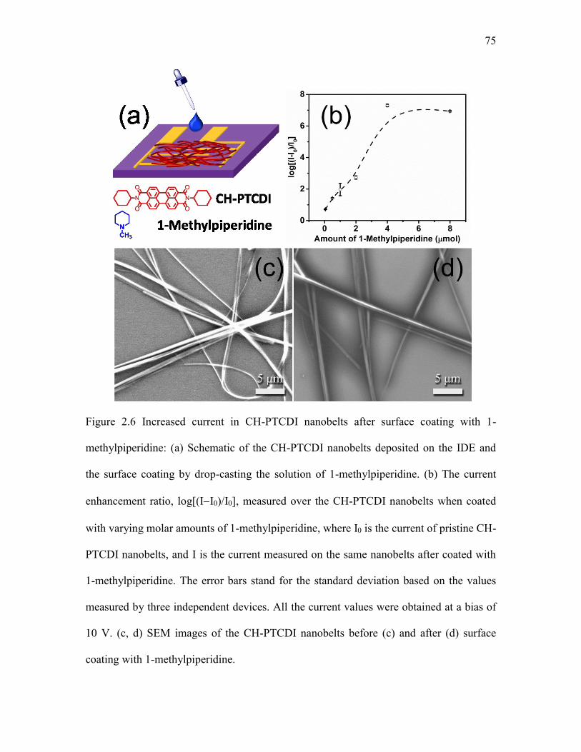
75
Figure 2.6 Increased current in CH-PTCDI nanobelts after surface coating with 1-
methylpiperidine: (a) Schematic of the CH-PTCDI nanobelts deposited on the IDE and
the surface coating by drop-casting the solution of 1-methylpiperidine. (b) The current
enhancement ratio, log[(II0)I0], measured over the CH-PTCDI nanobelts when coated
with varying molar amounts of 1-methylpiperidine, where I0 is the current of pristine CH-
PTCDI nanobelts, and I is the current measured on the same nanobelts after coated with
1-methylpiperidine. The error bars stand for the standard deviation based on the values
measured by three independent devices. All the current values were obtained at a bias of
10 V. (c, d) SEM images of the CH-PTCDI nanobelts before (c) and after (d) surface
coating with 1-methylpiperidine.

76
Figure 2.7 I-V curves of the CH-PTCDI nanobelts before (black) and after (red) surface
coating with 2 μmol 1-methylpieridine (MP). The pure 1-methylpiperidine thin film drop-
cast from 4 μmol amount is little conductive (blue).
0 3 6 9 12 151E-3
0.01
0.1
1
10
CH-PTCDI nanobelts
CH-PTCDI nanobelts + MP
Pure MP film
I (n
A)
Voltage (V)

77
300 400 500 600
0.00
0.05
0.10
0.15
0.20
0.25
500 550 600 650 700
(b)
Ab
so
rpti
on
Wavelength (nm)
MP-PTCDI
CH-PTCDI
MP-PTCDI
CH-PTCDI
Flu
ore
scen
ce I
nte
ns
ity (
a.u
.)
Wavelength (nm)
(a)
Figure 2.8 UV-vis absorption (a) and fluorescence (b) spectra of the chloroform solution
(10 μmolL1) of MP-PTCDI (black) and CH-PTCDI (red). The excitation wavelength for
fluorescence spectra was 490 nm.

78
Figure 2.9 Morphologies, UV-vis absorption, and fluorescence emission of PTCDI thin
films: (a, b) bright-field and fluorescent optical microscopy images of MP-PTCDI
nanoribbons deposited on a quartz slide; (c) UV-vis absorption (black) and fluorescence
(red) spectra of MP-PTCDI nanoribbons in the selected area (white cycle); (d, e) bright-
field and fluorescent optical microscopy images of CH-PTCDI nanobelts deposited on a
quartz slide; (f) UV-vis absorption (black) and fluorescence (red) spectra of CH-PTCDI
nanobelts in the selected area (white cycle).

79
500 550 600 650 700 750 800 0 20 40 60 80 100 1200
1
2
3
4
Flu
ore
scen
ce I
nte
nsit
y (
a.u
.)
Wavelength (nm)
0
0.5
1
5
10
50
100
1-Methylpiperidine (mmol L-1)
(b)
y=0.021x+1.027
R2=0.9994
F/F
0
[Q] (mmol L-1)
(a)
Figure 2.10 Significant fluorescence quenching of CH-PTCDI molecule when interacting
with 1-methylpiperidine: (a) Fluorescence spectra of CH-PTCDI solution in chloroform
(10 μmolL1) upon addition of 1-methylpiperidine at varying concentrations. The
excitation wavelength was 490 nm. (b) Stern-Volmer plot of the fluorescence quenching
shown in panel A.

80
0
5
10
15
20
25
30
35 (b)
Triethylamine
HexylamineAniline
1-Methylpiperidine
(I-I
0)/
I 0
Methanol
0.5 mol
10-4
100
104
108
Triethylamine
8 mol
Hexylamine
8 mol
(I-I
0)/
I 0
1-Methylpiperidine
8 mol
Aniline
12 mol
(a)
Figure 2.11 Comparative study of current in CH-PTCDI nanobelts after surface doping
with various amines: (a) histogram of current enhancement ratio of CH-PTCDI nanobelts
upon surface coating of 0.5 μmol different amines (1-methylpiperidine, aniline,
hexylamine, triethylamine), methanol, which was used as the solvent for these amines,
was also tested as the control; (b) histogram of current enhancement ratio of CH-PTCDI
nanobelts upon surface-coating of much larger amount of amines (1-methylpiperidine 8
μmol, aniline 12 μmol, triethylamine 8 μmol, and hexylamine 8 μmol). The error bars
represent the standard deviation based on the values measured by three independent
devices of each sample. All current values in histogram were gained at a bias voltage of
10 V.

81
400 500 600 700 800 900 1000
0.00
0.05
0.10
0.15
0.20
0.25
600 700 800 900 1000
0.000
0.005
0.010
0.015
CH-PTCDI
CH-PTCDI+MP
CH-PTCDI+MP
in air for 5 min
CH-PTCDI+MP
in air for 10 min
Ab
so
rpti
on
Wavelength (nm)
(b) CH-PTCDI
CH-PTCDI+MP
CH-PTCDI+MP
in air for 5 min
CH-PTCDI+MP
in air for 10 min
Ab
so
rpti
on
Wavelength (nm)
(a)
Figure 2.12 Detection of PTCDI anionic radicals: (a) UV-vis absorption spectra of
deoxygenated DMSO solution of CH-PTCDI (10 μmolL1) before (black) and after (red)
addition of excessive 1-methylpiperidine (MP, 0.1 molL1), and the same solution after
exposed to air for 5 min (blue) and 10 min (dark cyan); (b) enlarged UV-vis absorption
spectra of panel a in the wavelength range of 600 nm to 1000 nm.

82
400 500 600 700 800 900 1000
0.00
0.05
0.10
0.15
0.20
0.25
600 700 800 900 10000.000
0.004
0.008
0.012
0.016(b)
CH-PTCDI+Hexylamine
CH-PTCDI+Triethylamine
CH-PTCDI+Aniline
Ab
so
rpti
on
Wavelength (nm)
CH-PTCDI+Hexylamine
CH-PTCDI+Triethylamine
CH-PTCDI+Aniline
Ab
so
rpti
on
Wavelength (nm)
(a)
Figure 2.13 Detection of PTCDI anionic radicals: (a) UV-vis absorption spectra of
deoxygenated DMSO solution of CH-PTCDI (10 μmolL1) in the presence of excessive
amine (0.1 molL1), hexylamine (black), triethylamine (red), aniline (blue); (b) enlarged
UV-vis absorption spectra of panel a in the wavelength range of 600 to 1000 nm.

83
Figure 2.14 Schematic of the conductivity enhancement of MP-PTCDI nanoribbons.

84
0 50 100 150 200 250 300 3504
6
8
10
12
14
16
18
0 4 8 12 16 20
0
10
20
30
40
50
60
I (n
A)
Time (s)
18.5 ppm H2O
2 vapor
(b)
(I0-I
)/I 0
(%
)
Concentration of H2O
2 vapor (ppm)
(a)
Figure 2.15 Real-time electrical current profile of a MP-PTCDI nanoribbon chemiresistor
sensor in response to H2O2 vapor: (a) current measured over the MP-PTCDI nanoribbons
in response to H2O2 vapor (18.5 ppm); (b) relative current change [(I0I)/I0 ()] as a
function of the concentration of H2O2 vapor, where I and I0 are the current measured
before and after exposure to H2O2 vapor, respectively. The error bars represent the
standard deviation of the relative current changes measured with three independent
sensors.

85
Figure 2.16 A plot demonstrating how to calculate the current decrease of MP-PTCDI
nanoribbons in response to H2O2 vapor.
0 50 100 150 200 250 300 3504
6
8
10
12
14
16
18
I (n
A)
Time (s)
18.5 ppm H2O
2 vapor I
0
I
I

86
0 100 200 300 400 500 600
0
4
8
12
16
(I-I
0)/
I 0 (
%)
Time (s)
Acetone
Ethyl acetate
Dichloromethane
Methanol
Water
Ethanol
Toluene
Hexane
5% saturated chemical
vapor at 20 C
0
2
4
6
8
10
12
14(b)
(I-I
0)/
I 0 (
%)
Acetone
12800 ppm
5% saturated chemical vapor at 20 C
Ethyl acetate
4900 ppm
Dichloromethane
25000 ppm
Methanol
6600 ppm
Water
1100 ppm
Ethanol
3000 ppm
Toluene
1500 ppm
Hexane
8400 ppm
(a)
Figure 2.17 The selectivity of a MP-PTCDI nanoribbon chemiresistor sensor: (a) relative
current change ((II0)I0) of MP-PTCDI nanoribbons in three subsequent exposures
toward the common organic liquids and water at 5 of the saturated vapor concentration;
(b) average values of (II0)I0 measured over the MP-PTCDI nanoribbons when exposed
to the different liquids vapor at 5 saturated vapor concentration. The error bars
represent the standard deviation of the relative current changes measured with three
independent sensors.

87
Table 2.1 Comparison of morphology and size of PTCDI-based nanostructures.
Sample Morphology Thickness Width Length Reference
MP-PTCDI Nanoribbon About 15
nm 100-300 nm
Several
micrometers This work
MA-PTCDI Nanoribbon About 5 nm 50-200 nm Several
micrometers S1
MO-PTCDI Nanoribbon - 30-500 nm - S1

88
Table 2.2 The dipole moment of the liquid analytes tested and the corresponding sensor
response measured at 5% of the saturated vapor concentration.
Analyte μ (Debye) (II0)I0 ()
Acetone 2.88 8.19
Ethyl acetate 1.78 5.40
Dichloromethane 1.60 3.71
Methanol 1.70 3.14
Water 1.85 2.13
Ethanol 1.69 1.28
Toluene 0.36 0.86
Hexane ≤ 0.1 0.10

CHAPTER 3
PERSISTENT PHOTOCONDUCTIVITY IN PERYLENE
DIIMIDE NANOFIBER MATERIALS1
3.1 Abstract
Perylene tetracarboxylic diimide (PTCDI) derivatives have been extensively
investigated for one-dimensional (1D) self-assembly and their applications in
optoelectronic devices. Our study on self-assembled PTCDI nanofiber materials revealed
a persistent photoconductivity (PPC) effect, which is sustained conductivity after
illumination is terminated. A comprehensive understanding of the PPC effect in PTCDI
nanofibril materials will enable us to explore and enhance their optoelectronic
applications. Here, we have investigated the PPC effect in the nanofibers assembled from
1-Methylpiperidine-substituted perylene tetracarboxylic diimide (MP-PTCDI) with
respect to the PPC relaxation at different temperatures, illumination power densities,
molar amount and morphology of the PTCDI film deposited on the interdigitated
electrodes. The photocurrent relaxation was also performed on several other PTCDI
nanofiber materials for comparative study. We conclude that the significant PPC effect in
1 Reproduced by permission from Wu, N.; Wang, C.; Slattum, P. M.; Zhang, Y; Yang, X.;
Zang, L., Persistent Photoconductivity in Perylene Diimide Nanofiber Materials. ACS
Energy Lett. 2016, 1, 906-912. Copyright (2016) American Chemical Society.
90
MP-PTCDI nanofibers can be attributed to the electrical potential fluctuations caused by
the structure defects, which thus hinder the recombination of charge carriers. This study
may provide new design rules for fabrication of molecular semiconductor materials with
strong PPC in order to approach high efficiency of photovoltaic and photocatalysis.
3.2 Introduction
Perylene tetracarboxylic diimide (PTCDI) derivatives, forming a typical n-type
organic semiconductor, have been receiving much research attention because of their
high thermal- and photo-stability.1,2 Their strong electron affinity and strong absorption
in the visible light region make PTCDI a good candidate for next-generation photovoltaic
devices3-6 and photocatalytic materials.1,7 In addition, self-assembly of PTCDI molecules
often gives rise to the formation of well-defined nanofibril structures through the
columnar π-π stacking between the perylene planes.2 The as-prepared PTCDI nanofibers
assist in the construction of the distinctive morphology of p-n junction nanostructures in
photovoltaic devices to improve their performance,4,6 for instance, the novel crystalline
donor/acceptor (P3HT/PTCDI) shish-kebab structure,4,8 in which the observed high
photovoltage was likely due to this special intermolecular orientation. PTCDI nanofibril
materials have the potential to be used in photocatalytic systems as well. Previous
research has shown that PTCDI molecules with attached donor moieties were self-
assembled into nanofibers, followed by coated with co-catalysts, such as TiO2 and/or
Pt,1,7 or g-C3N4 and Pt,9 showed excellent performance in the photocatalytic splitting of
water for H2 production. The excellent photocatalytic activity of the composite
photocatalysts was attributed to PTCDIs’ strong visible-light absorption, matched energy

91
level and effective charge separation with the co-catalysts.1,7
In this study, persistent photoconductivity (PPC), which is sustained conductivity
after illumination is terminated,10 was observed by accident in the nanofibers fabricated
from a PTCDI molecule with a Donor-Acceptor (D-A) structure (1-Methylpiperidine
substituted-PTCDI molecule, MP-PTCDI, shown in Figure 3.1). In general, the PPC
effect is not so commonly observed in organic semiconductor materials as in inorganic
counterparts. For PTCDI-based materials there have been few reports where the PPC
effect was implied.11,12 We believe that further study of the PPC effect and the
dependence on materials structure will offer deep insight into the charge carrier storage
and relaxation process within organic semiconductor materials (particularly PTCDIs),
thus providing guidance in optimizing the photovoltaic and photocatalytic performance of
these materials.
The PPC effect has been mostly observed and investigated in inorganic
semiconductor compounds, alloys and heterojunctions.10,13-17 Generally, the PPC effect is
caused by a potential barrier that prohibits the recombination of photogenerated electron-
hole pairs. There are multiple models to describe the PPC mechanism in regard to various
material systems, such as random localized potential fluctuations (RLPF), large lattice
relaxation (LLR) and microscopic barrier (MB).10 In the RLPF model, carriers are
separated by the potential fluctuations, which reduce the rate of recombination, producing
PPC. For example, RLPF induced by composition fluctuation was found to be
responsible for PPC observed in Zn0.3Cd0.7Se mixed crystals13 and CdS0.5Se0.5
semiconductor alloy.15 In addition to the intrinsic sources, extrinsic origins of RLPF may
also come from the substrate effect as was found in monolayer MoS2 field effect

92
transistors.10 In a LLR model, deep-level traps (DX centers) are considered to be the
source of PPC. Under illumination, the DX center can be converted into a metastable
shallow donor state, which produces a potential barrier due to the difference in lattice
relaxation between the two states. The recapture of electrons by the DX center is
prevented by the barrier, leading to the PPC effect.17,18 The LLR model was supported by
a study on n-type AlxGa1-xAs, for which the PPC effect was produced by donor-related
defects.18 The MB model is based on the spatial macroscopic potential barrier, which
separates the photoexcited electron-hole pairs, and this model explains well the PPC
effect in many heterostructures, such as graphene/MoS2,16 quantum-dot/graphene,19
chlorophyll/graphene.20
Although the PPC effect, as well as its influence on optoelectronic properties and
performance, have been extensively studied on the inorganic semiconductors, there lacks
of such detailed study on the organic materials. Especially, most of the PPC studies have
been performed at low temperatures (e.g., from 17 K to 300 K).14 Room temperature
study of the PPC within organic materials would fill in the field with new knowledge by
understanding better the sustained photoinduced charge separation.21-23 In this work, an
electron donor-acceptor PTCDI, MP-PTCDI (Figure 3.1), was chosen as the organic
semiconductor material to study the PPC effect. For comparison, several other PTCDIs
were also employed and investigated parallel under the same conditions. Moreover, the
PTCDIs form well-defined nanofibers through solution phase self-assembly, and the 1D
intermolecular arrangement (dominated by the cofacial stacking) provides efficient
charge transport pathway, which further enhances the charge separation and is suited for
application in photocatalysis and photovoltaics.24 As observed in this study, the PPC

93
decay time of MP-PTCDI nanofibers can be as long as 1058 s. The PPC decay was found
to be dependent on the temperature, the irradiation power density, the film morphology
and amount of nanofibers deposited on the interdigitated electrodes (IDE). Moreover, the
side groups of PTCDI can be modified with electron donating moieties with different
donation power (as shown in Figure 3.1), in order to investigate the influence of electron
donor-acceptor interaction on the PPC. Donor-acceptor interaction, particularly under
photoexcitation, creates charge separation and electrostatic traps, thus producing potential
barriers that hinder the recombination of electron-hole pairs. Since the two imide
positions within PTCDI are nodes in the -orbitals, changing the substitutions at the two
ends does not change significantly the electronic properties of PTCDI.24,25 This enabled
us to perform the comparative PPC studies employing different PTCDI molecules shown
in Figure 3.1, from which the effect of electron donating group can be investigated.
3.3 Experimental Section
3.3.1 Synthesis of PTCDI Molecules and Fabrication
Into Nanofiber Structures
The synthesis of MP-PTCDI, MA-PTCDI, MO-PTCDI, DD-PTCDI and CH-PTCDI
followed the methods reported in our previous papers.26-29 MT-PTCDI was synthesized
similarly, as briefly described below. First, N-dodecyl-perylene-3,4,9,10-tetracarboxy
monoimide monoanhydride was synthesized using the previously reported method.26,27 50
mg of the syntehsized monoanhydride was mixed with 4-(dimethylamino)butylamine
(Sigma-Aldrich, 31.0 mg), zinc acetate (Sigma-Aldrich, ACS reagent, 98%, 1.0 mg) and
imidazole (Sigma-Aldrich, ACS reagent, > 99%, 750.0 mg) in a tightly capped vial and

94
heated at 125 °C for 4 hours under magnetic stirring. The reaction was then terminated
and cooled to room temperature, followed by addition of 2 N HCl solution to dissolve the
imidazole. The red suspension was collected by filtration using 0.45 m membrane filter
and washed with distilled water and methanol. The red solid obtained was then dispersed
in CHCl3 (200 mL) and washed with saturated NaHCO3 (Sigma-Aldrich, ACS reagent, ≥
99.7%), water, brine and dried over Na2SO4 (Sigma-Aldrich, ACS reagent, > 99%). The
product was then recrystallized from CHCl3/CH3CN and vacuum dried to afford 53.9 mg
product (92%) as a very dark red solid. 1H NMR (300 MHz, CDCl3, TMS, ppm): δ = 8.55
(d, J = 6.0 Hz, 4H; perylene H), 8.45 (d, J = 6.0 Hz, 4H; perylene H), 4.244.16 (m, 4H;
(CO)2NCH2), 2.35 (m, 2H; CH2*N(CH3)2), 2.24 (s, 6H; N(CH3)2), 1.861.18 (m, 24H;
12CH2), 0.87 (t, J = 6.0 Hz, 3H; CH2CH3*). MALDI-TOF-MS: [M+H+]/z = 658.43.
The nanofibers were fabricated by injecting 1 mL of a chloroform solution of the
PTCDI compound (0.1 mmol L) into 5 mL of ethanol. The nanofibers were formed
after aging at room temperature in dark overnight.
3.3.2 In Situ PTCDI Nanofiber Fabrication on a Substrate
The MP-PTCDI thin film was prepared by drop-casting 10 μL MP-PTCDI solution in
chloroform (0.1 mmol L1) on a silicon substrate covered with 300 nm thick SiO2 layer
(with or without the pre-patterned IDEs). The freshly prepared thin film was dried in air
for 1 h, or aged in an oven at 60 °C for 72 h, or annealed with ethanol vapor in a sealed
chamber for 24 h. The ethanol-vapor annealing was conducted by placing the MP-PTCDI
thin films into a sealed 60 mL jar, in which a 5 mL vial containing ethanol was placed to
maintain the saturated vapor of ethanol. The films were kept in the vapor environment for

95
24 h to complete the annealing process.
3.3.3 MP-PTCDI Nanofibers Embedded in PEG-PPG-PEG
Triblock Copolymer Matrix
The poly(ethylene glycol)-block-poly(propylene glycol)-block-poly(ethylene glycol)
(PEG-PPG-PEG, average Mn ~1100, Sigma-Aldrich) was dissolved in ethanol. 10 μL
MP-PTCDI solution in chloroform (0.1 mmol L1) was injected into the above PEG-
PPG-PEG/ethanol solution (100 μL). The mass ratio of MP-PTCDI to PEG-PPG-PEG in
this mixture is 10:1. After aging the mixture in dark overnight, the MP-PTCDI nanofibers
were formed in situ in the polymer matrix and could be transferred onto the substrate for
further measurements.
3.3.4 Materials Characterization
UV−vis absorption spectra were acquired with an Agilent Cary 100 UV-visible
spectrophotometer. Fluorescence spectra were collected with an Agilent Eclipse
spectrophotometer. SEM measurement was performed on an FEI Nova Nano 630 (FEI
Corporation) with a helix detector in low vacuum (0.43 Torr water pressure). AFM
measurements were performed on a Veeco MultiMode V scanning probe microscope in
tapping mode. A silicon substrate coated with a polished 300 nm thick SiO2 layer was
used as the substrate for both AFM and SEM measurements. The bright field and
fluorescence optical microscopy images were obtained with a Leica DMI4000B inverted
microscope equipped with an Acton SP-2356 Imaging Spectrograph system and
Princeton Instrument Acton PIXIS: 400B Digital CCD Camera System. X-ray diffraction

96
patterns of PTCDI nanofiber thin films were obtained using a Bruker D2 Phase X-ray
diffractometer with Cu Kα (λ = 1.5418 Å). The thin films for XRD measurement were
prepared by drop-casting PTCDI nanofibers onto a clean glass slide substrate (D = 1.5
cm). Kelvin probe force microscopy (KPFM) was achieved on Bruker Dimension Icon
scanning probe microscope. The surface potential was measured using Lift Mode with a
conductive antimony doped silicon tips (SCM-PIT, Bruker) along with a cantilever
coated with 20 nm Pt/Ir on both sides. Indium-doped tin oxide (ITO) coated glass slides
(Delta Technology, R = 5-15 Ω) were used as the substrate for KPFM measurements.
3.3.5 Electrical Current Measurement
Interdigitated electrodes (IDEs) were used for all electrical current measurements in
this work. The IDEs have a channel width of 2100 μm and a gap length of 80 μm, and
was fabricated by a standard photolithography procedure on a silicon wafer covered with
a 300 nm thermal oxide layer (Silicon Quest International). The electrodes were patterned
by sputtering with 20 nm thick titanium adhesion layer and 50 nm thick gold layer. The
electrical conductivity was measured under ambient conditions using a two-probe method
on a Signatone S-1160 Probe Station combined with an Agilent 4156C Precision
Semiconductor Analyzer. The I-V curves were measured for all the six PTCDI nanofibers
both under dark and illumination in the bias range of 0-15 V. Typical I-V curves are
shown in Figure 3.2. Although most nanofibers show linear relationship, some nanofiber
like DD-PTCDI showed roughly two linear ranges, with smaller slope in low bias and
higher slope in higher bias for the photocurrent. Therefore, the medium bias of 7 V was
chosen for the photocurrent and PPC measurements. A tungsten lamp (Quartzline, 21 V,

97
150 W) was used as the white light source, and the light is guided into the probe station
through a glass optical fiber, followed by focusing on the sample through the objective
lens. The tungsten lamp used in this study provides white light covering from 400 nm to
900 nm, as measured in our previous study.30 This white light was used here because it
provides the visible light with energy in the absorption region of the PTCDI nanofibers
(400-650 nm, Figure 3.3), which can initiate the highest occupied molecular orbital
(HOMO) to lowest unoccupied molecular orbital (LUMO) transition of PTCDI,27 thus
enabling the electron transfer from the amine (lone pair) to the one-electron missed
HOMO of singlet state of PTCDI. The irradiation power density can be adjusted with the
illuminator (Dolan-Jenner Fiber-Lite MI-150 Fiber Optical Illuminator, 150 W). The
optical power reaching the sample surface was measured by a power meter (Mells Griot
broadband power/energy meter, 13PEM001). All the samples used for persistent
photoconductivity study were stored under vacuum in dark at room temperature for two
days before the measurement. To compare the persistent photoconductivity of different
PTCDIs, the nanofibers were assembled by injecting 10 μL PTCDI solution in
chloroform (0.1 mmol L1) into 100 μL ethanol. The as-assembled nanofibers were
dispersed well in ethanol, followed by being transferred onto the IDEs by slow drop-
casting to ensure uniform coverage over the whole IDEs area. To study the temperature
dependent PPC, the IDEs chip was placed on a heating stage, of which the temperature
was controlled by a temperature controller (INSTEC, STC 200).

98
3.4 Results and Discussions
Figure 3.4 shows the PPC results obtained with the MP-PTCDI nanofibers deposited
on IDEs. After maintaining a stable current in dark, the MP-PTCDI nanofibers were then
illuminated by white light with a spot size covering the whole nanofiber area. The
nanofibers demonstrated high photoconductivity upon illumination, producing a
photocurrent on/off ratio ranging from ca. 18 to 71 with the illumination power density
increasing from 0.31 to 5.77 mW cm-2 under a bias voltage of 7 V (Figure 3.4a and
Table 3.1). After termination of illumination, the photocurrent relaxed quite slowly to the
dark current level, and the decay rate depends significantly on the illumination power
density (Figure 3.4b). The PPC decay curves can be well-fitted by a single stretched
exponential decay (Equation 3.1), namely Kohlrausch’s law, as widely reported in the
literature on PPC effect,10,13
𝐼(𝑡) = 𝐼0exp [−(𝑡 𝜏)]𝛽⁄ (0 < 𝛽 < 1) 3.1
where I0 is the photocurrent before the illumination is removed, τ is the decay time
constant, representative of the time scale of the decay process, and β is the deviation from
a single-exponential decay. The decay time constant τ of the MP-PTCDI nanofibers under
illumination with various illumination power densities are shown in Figure 3.4c and
summarized in Table 3.1. It is noted that the decay time constant decreases with the
increase of illumination power density. Upon increasing the illumination power density, a
higher concentration of free charger carriers should be produced within the MP-PTCDI
nanofibers,11,24,27 as evidenced by the increased photocurrent on/off ratio and the shorter

99
time required for achieving photocurrent equilibrium (Table 3.1). The higher
concentration of free charge carriers leads to a greater probability of recombination of
charge carriers, and consequently faster decay of the photocurrent. The PPC observed
with the MP-PTCDI nanofibers was also found reproducible as confirmed by cycling on
and off the illumination in 300 s intervals (Figure 3.4d). When the light was turned on,
the current increased rapidly. Upon termination of the illumination, the current dropped
to about 50% of the photocurrent within 300 s in the first cycle, and this “on” and “off”
photoswitching remained reversible and reproducible in the following cycles. The lowest
current obtained at 300 s after the termination of light still stays at the level of about 50%
of the maximal photocurrent generated in the first cycle, though the photocurrent
generated in the later cycles drifted lower to some extent, likely due to the
photooxidation,27,31-33 as the experiments were run in air.
We also observed the wavelength dependence of the photoconductivity and PPC
effect of MP-PTCDI nanofiber materials by using long-pass filters with cut-on
wavelength of 550 and 700 nm, while keeping the flux of photons constant in both cases.
As shown in Figure 3.5, with the 550 nm filter, the photocurrent on-off ratio obtained for
MP-PTCDI nanofibers was ca. 19 and a significant PPC effect was observed with decay
time of 269 s, whereas when 700 nm filter was used, there was no photoconductivity
obtained for the same nanofibers, simply because the wavelength above 700 nm has less
than the bandgap energy to initiate the HOMO to LUMO transition of PTCDI.27
As extensively investigated with GaN, the PPC effect was found to be structure
dependent.34,35 For example, when fabricated as nanorods, the PPC effect of GaN was
strongly related to the diameter of nanorods,34 and a further enhanced PPC was observed

100
in nanoporous GaN formed by electrochemical etching.35 Inspired by such research work
on inorganic materials, we attempted to study how the structure (morphology) of MP-
PTCDI materials would affect the PPC as observed in Figure 3.4. Taking advantage of
the ease of molecular self-assembly of PTCDIs, the morphology of MP-PTCDI materials
can be controlled via evaporation induced molecular assembly on the oxidized surface of
silicon wafer (or silicon wafer pre-patterned with IDEs). Such in situ fabrication method
allowed us to tune the morphology of molecular aggregates through thermal and solvent
vapor annealing.36 The AFM images in Figure 3.6 indicate the evolution of the MP-
PTCDI nanofiber structure from the initially disordered particulate aggregate under
different annealing processes. The drop-cast thin film formed directly from the
evaporation in air showed partially dewetted patterns, and there was no obviously
structure or ordered morphology (Figure 3.6a). By annealing at 60 °C for 72 h, an
approximately uniform and worm-shaped pattern formed in the film (Figure 3.6b). Upon
annealing in the vapor of ethanol (a poor solvent for MP-PTCDI) for 24 h, well-defined
nanofiber structures were established (Figure 3.6c), where the dimension of the
nanofibers is about 500-800 nm in length, and 200 nm in width. We investigated the PPC
effect with the three MP-PTCDI thin films annealed under different conditions, and the
results are shown in Figure 3.6d. The as prepared thin film shows the fastest decay in
current (with τ = 53±3 s), followed by the film thermally annealed at 60 °C (τ = 93±6 s),
and the nanofiber film annealed in ethanol vapor shows the slowest decay (τ = 119±10
s). Clearly, the self-assembled 1D nanostructure with the most organized molecular
packing through π-π stacking enhances the PPC effect in MP-PTCDI.
The PPC was also found to be dependent on the molar amount of MP-PTCDI

101
nanofibers deposited on the IDEs. The decay time constant increased with the molar
amount of nanofibers, while the rate of increase slowed when more than 1 nmol of
nanofibers were deposited, mainly because the efficient conductive channel of MP-
PTCDI nanofibers becomes saturated on the IDEs used (Figure 3.7). We also investigated
the PPC in a control sample, in which MP-PTCDI nanofibers were dispersed in a PEG-
PPG-PEG polymer matrix. Upon dispersing in polymer matrix, the inter-fiber contact
would be insulated by the polymer, thus excluding the possibility that the inter-fiber
contact (junction) may contribute to the observed PPC. As expected, the average width of
the fibers is now 200 nm larger than the value of pristine MP-PTCDI nanofibers due to
the surface coating of polymers (Figure 3.8). The almost identical PPC observed in the
control sample (Figure 3.9, the decay time of 103 s and 102 s for the pristine MP-PTCDI
nanofibers and those embedded in polymer, respectively) suggested negligible
contribution from the junctions of nanofibers. The origin of the PPC effect should be
correlated to nanofiber structure and the 1D crystal lattice.
To further explore the mechanism of the observed PPC effect in the MP-PTCDI
nanofibers, a series of other PTCDI molecules with different side groups were studied for
comparison. Most of these PTCDIs contain a linear dodecyl chain on one side, but with
different groups on the other side; CH-PTCDI is the only symmetric molecule with both
sides substituted with cyclohexane group (Figure 3.1). All these PTCDIs were fabricated
into nanofibers following the similar self-assembly process and investigated for the PPC
under the same conditions as used for MP-PTCDI nanofibers. Interestingly, PPC was
only found in the nanofibers fabricated from the PTCDIs substituted with strong electron-
donating groups, such as MP-PTCDI, MT-PTCDI and MA-PTCDI (Figure 3.10), where

102
the PPC decay curves can be fitted with a single stretched exponential equation, as
widely reported in the literature on PPC effect,10,13 although the whole decay has a long
tail that takes more than 1 h to reach the dark current baseline. In contrast, no significant
PPC effect was observed for the nanofibers of PTCDIs with weak electron donors (e.g.,
MO-PTCDI, DD-PTCDI and CH-PTCDI), for which the photocurrent returned relatively
quickly to the dark current level in less than 10 s, and the PPC decay curves of which do
not fit into the same exponential equation (Equation 3.1), implying no significant PPC
effect.
All the six PTCDI molecules employed in this work were found to form well-defined
nanofibers as evidenced in Figure 3.8a, Figure 3.11 and our previous self-assembly
studies.26-29 The X-ray diffraction (XRD) patterns also indicate highly ordered 1D
columnar microstructures, with the inter-columnar spacing determined by the well-
defined peaks around 4.0°, to be 23.43, 21.08, 22.25, 27.35, 25.38 and 18.10 Å for MP-,
MT-, MA-, MO-, DD- and CH-PTCDI nanofibers, respectively (Figure 3.12).28,29,37,38
However, the detailed molecule packing patterns are different as revealed by XRD
patterns because the side group modification affects the molecular packing.25,28,37 From
our observation and results in Figure 3.10, it is unlikely that the different molecular
packing or slight difference in morphology contributes significantly to the PPC. For
example, even though DD-PTCDI and CH-PTCDI demonstrate great difference in
molecular packing due to the side group effect (slipped stacking along the [100] direction
for DD-PTCDI39,40 vs. flip-flap stacking for CH-PTCDI along the [100] direction29), none
of them demonstrates significant PPC, implying that tuning the molecular packing does
not likely produce PPC. Therefore, the observed PPC is more of correlation with the

103
donor-acceptor structure of PTCDI, which creates charge separation state through
photoinduced electron transfer from the donor (the amine moiety) to acceptor (the PTCDI
central core).27,41 While the photoinduced electron transfer primarily occurs through an
intramolecular process, it can also happen via an intermolecular process when the donor
and acceptor are arranged in close proximity in the molecular assembly of
nanofibers.26,42,43 The charge separation between donor and acceptor can further be
enhanced by the efficient electron delocalization along the π-π stacking of PTCDI
planes.2,24,26,27,44 When the charge (negative or positive) is trapped at a molecule site, it
may change the local dipole moment and the molecule orientation in the stacking as well,
thus creating a local defect. It has also been widely argued in literatures that charge traps
may come from the donors (acting as nucleophilic sites) and acceptors (as electrophilic
sites) depending on the D-A association, which in turn can be controlled by the D-A
strength and relative ratio of D and A moieties, as applied in memory devices.45 The
electrostatic potential fluctuation around the defect acts as an energy barrier preventing
the charge recombination between electrons and holes, leading to PPC, similar to what
was observed in inorganic semiconductor materials as described by the RLPF model.10,13-
17
The photoinduced charge separation within the MP-PTCDI nanofibers can be
confirmed by Kelvin probe force microscopy measurement (KPFM), which images the
surface potential change of material caused by charge separation.43,46,47 As shown in
Figure 3.13a, well-defined morphology of the MP-PTCDI nanofibers was imaged by the
tapping mode AFM. Figure 3.13b and d show the surface potential images of MP-PTCDI
nanofibers in dark and after illumination, respectively. The statistic distributions of the

104
relative surface potential measured accordingly are plotted in Figure 3.13c and e. Upon
illumination, the surface potential of MP-PTCDI nanofibers became more negative
(about -13 mV shift), indicating the significant charge separation driven by
photoexcitation, which has been confirmed by the transient absorption spectral study.48
In addition to the photoinduced charge separation, strong electron donor can also
initiate charge separation in the dark through steady state charge-transfer interaction
between the MP moiety (1-Methylpiperidine moiety) on one molecule and the PTCDI
part on the other molecule, as recently observed in our lab on the MP-PTCDI
nanofibers26 and other PTCDI materials.44,49 The pre-formed charge carriers not only
increase the electrical conductivity, but meanwhile also create more structural defects that
enhance the PPC as discussed above. In contrast, the nanofibers of MA-PTCDI did not
demonstrate such dark conductivity due to the lack of effective charge-transfer
interaction between MA (N,N-Dimethylaniline moiety) and PTCDI, and as a result, the
PPC effect observed was minimal compared to that of MP-PTCDI (Figure 3.10) likely
due to the intrinsically low density of defects in MA-PTCDI material. On the other hand,
significant PPC was observed for the nanofibers of MT-PTCDI (Figure 3.10), which can
be attributed to the high density of charge carriers in steady state and the more defects
thus created, similar to the case of MP-PTCDI. To confirm the steady state charge
transfer within MT-PTCDI nanofibers, we measured the fluorescence of both the
molecular solution in chloroform (Figure 3.14) and the nanofibers deposited on quartz
surface (Figure 3.15). The strong fluorescence measured for the MT-PTCDI molecules
implies no photoinduced intramolecular electron transfer, which is consistent with the
long donor-acceptor distance between the terminal amine and PTCDI.26,27,50 However,

105
when assembled into nanofibers the MT-PTCDI molecules stack closely together, thus
bringing the MT (N,N-Dimethylbutylamine moiety) and PTCDI moieties in proximity,
allowing for effective charge transfer interaction, as supported by the complete
fluorescence quenching in the nanofiber state (Figure 3.15). Such strong intermolecular
charge transfer interaction would increase the charge carrier density, as well as the
defects that account for the significant PPC observed. The increased charge carrier
density within MT-PTCDI nanofibers was also evidenced by the high dark current
measured (0.008 A at a bias of 7 V), comparable to that of MP-PTCDI nanofibers
(0.010 A at a bias of 7 V), but much higher than that of MA-PTCDI nanofibers (7.0 ×
105 A at a bias of 7 V), which were all measured under the same conditions.
According to the RLPF model,10,13-17 we attribute the observed PPC in PTCDI
nanofibers to the charge relevant defects, which generate a potential barrier preventing
the recombination of photogenerated charge carriers. The potential barrier can be
estimated from the temperature dependent measurement of the PPC decay kinetics.
Figure 3.16 shows the typical PPC decay curves measured on the MP-PTCDI nanofibers
at different temperatures. It is clearly seen that the PPC effect gets more significant with a
decrease in temperature. The decay time constants extracted from the curves show rapid
decreasing at higher temperature (Figure 3.17). This temperature dependence indicates a
typical thermally activated process for the charge recombination, which can be described
by an Arrhenius equation (Equation 3.2),14,35
𝜏 = 𝜏0exp [∆𝐸 𝑘𝐵𝑇⁄ ] 3.2
106
where τ is the decay time constant at any experimental temperature, τ0 is the decay time
constant at temperature of zero K, E is the potential barrier of the charge recombination,
kB is the Boltzmann constant, and T is the temperature in the unit of Kelvin. Logarithmic
plot of τ as a function of 1/T should give a linear relationship (R2 = 0.9840) as indeed
shown in Figure 3.16b. The slope of the linear fit gives value of potential barrier, 137
meV. This value is on the same level as those reported for n-type GaN.14,17 This high
activation barrier helps prevent the charge recombination, thereby enhancing the
photovoltaic or photocatalytic efficiency when these PTCDIs are used as the
photoresponsive materials.
3.5 Conclusions
In conclusion, we have studied the PPC effect in PTCDI nanofiber materials. It was
found that the PTCDIs containing strong electron donor groups demonstrated significant
PPC effect when fabricated into nanofiber materials. This is likely due to the defects
formed from the charge separation within the molecular stacks, wherein electrical
potential barrier created around the defects prevent the recombination of the
photogenerated charge carriers. The extended electron delocalization along the π-π
stacking (the long axis of nanofiber) further enhances the charge separation, creating
more charge relevant defects, resulting in more pronounced PPC. Since the charge
recombination is typically a thermally activated process, the PPC shows strong
temperature dependence. Linear fitting between the PPC decay time and temperature
gives estimation of the activation barrier (energy), 137 meV, which is comparable to that
obtained for the inorganic semiconductors such as n-type GaN. This work provides, for

107
the first time, systematic investigations on the PPC effect in PTCDI based materials
(particularly the nanofibers), and the results will help understand the mechanism and
design new material structures for sustained charge separation in order to further enhance
the photovoltaic and photocatalytic efficiency of organic semiconductor materials.
3.6 References
(1) Chen, S.; Slattum, P.; Wang, C.; Zang, L. Self-Assembly of Perylene Imide
Molecules Into 1D Nanostructures: Methods, Morphologies, and Applications. Chem.
Rev. 2015, 115, 11967-11998.
(2) Zang, L.; Che, Y.; Moore, J. S. One-Dimensional Self-Assembly of Planar π-
Conjugated Molecules: Adaptable Building Blocks for Organic Nanodevices. Acc. Chem.
Res. 2008, 41, 1596-1608.
(3) Hains, A. W.; Liang, Z.; Woodhouse, M. A.; Gregg, B. A. Molecular
Semiconductors in Organic Photovoltaic Cells. Chem. Rev. 2010, 110, 6689-6735.
(4) Li, L.; Jacobs, D. L.; Bunes, B. R.; Huang, H.; Yang, X.; Zang, L. Anomalous High
Photovoltages Observed in Shish Kebab-Like Organic p-n Junction Nanostructures.
Polym. Chem. 2014, 5, 309-313.
(5) Kim, J. Y.; Bard, A. J. Organic Donor/Acceptor Heterojunction Photovoltaic Devices
Based on Zinc Phthalocyanine and a Liquid Crystalline Perylene Diimide. Chem. Phys.
Lett. 2004, 383, 11-15.
(6) Wicklein, A.; Ghosh, S.; Sommer, M.; Würthner, F.; Thelakkat, M. Self-Assembly of
Semiconductor Organogelator Nanowires for Photoinduced Charge Separation. ACS
Nano 2009, 3, 1107-1114.
(7) Chen, S.; Jacobs, D. L.; Xu, J.; Li, Y.; Wang, C.; Zang, L. 1D Nanofiber Composites
of Perylene Diimides for Visible-Light-Driven Hydrogen Evolution From Water. RSC
Adv. 2014, 4, 48486-48491.
(8) Bu, L.; Pentzer, E.; Bokel, F. A.; Emrick, T.; Hayward, R. C. Growth of
Polythiophene/Perylene Tetracarboxydiimide Donor/Acceptor Shish-Kebab
Nanostructures by Coupled Crystal Modification. ACS Nano 2012, 6, 10924-10929.
(9) Chen, S.; Wang, C.; Bunes, B. R.; Li, Y.; Wang, C.; Zang, L. Enhancement of
Visible-Light-Driven Photocatalytic H2 Evolution from Water over g-C3N4 through
Combination With Perylene Diimide Aggregates. Appl. Catal., A 2015, 498, 63-68.
(10) Wu, Y.-C.; Liu, C.-H.; Chen, S.-Y.; Shih, F.-Y.; Ho, P.-H.; Chen, C.-W.; Liang, C.-

108
T.; Wang, W.-H. Extrinsic Origin of Persistent Photoconductivity in Monolayer MoS2
Field Effect Transistors. Sci. Rep. 2015, 5, 11472.
(11) Mukherjee, B.; Sim, K.; Shin, T. J.; Lee, J.; Mukherjee, M.; Ree, M.; Pyo, S.
Organic Phototransistors Based on Solution Grown, Ordered Single Crystalline Arrays of
a π-Conjugated Molecule. J. Mater. Chem. 2012, 22, 3192-3200.
(12) Draper, E. R.; Walsh, J. J.; McDonald, T. O.; Zwijnenburg, M. A.; Cameron, P. J.;
Cowan, A. J.; Adams, D. J. Air-Stable Photoconductive Films Formed From Perylene
Bisimide Gelators. J. Mater. Chem. C 2014, 2, 5570-5575.
(13) Jiang, H. X.; Lin, J. Y. Persistent Photoconductivity and Related Critical
Phenomena in Zn0.3Cd0.7Se. Phys. Rev. B: Condens. Matter Mater. Phys. 1989, 40,
10025-10028.
(14) Chen, H. M.; Chen, Y. F.; Lee, M. C.; Feng, M. S. Yellow Luminescence in n-Type
GaN Epitaxial Films. Phys. Rev. B: Condens. Matter Mater. Phys. 1997, 56, 6942-6946.
(15) Dissanayake, A. S.; Huang, S. X.; Jiang, H. X.; Lin, J. Y. Charge Storage and
Persistent Photoconductivity in a CdS0.5Se0.5 Semiconductor Alloy. Phys. Rev. B:
Condens. Matter Mater. Phys. 1991, 44, 13343-13348.
(16) Roy, K.; Padmanabhan, M.; Goswami, S.; Sai, T. P.; Ramalingam, G.; Raghavan, S.;
Ghosh, A. Graphene-MoS2 Hybrid Structures for Multifunctional Photoresponsive
Memory Devices. Nat. Nanotechnol. 2013, 8, 826-830.
(17) Hirsch, M. T.; Wolk, J. A.; Walukiewicz, W.; Haller, E. E. Persistent
Photoconductivity in n-Type GaN. Appl. Phys. Lett. 1997, 71, 1098-1100.
(18) Lang, D. V.; Logan, R. A. Large-Lattice-Relaxation Model for Persistent
Photoconductivity in Compound Semiconductors. Phys. Rev. Lett. 1977, 39, 635-639.
(19) Konstantatos, G.; Badioli, M.; Gaudreau, L.; Osmond, J.; Bernechea, M.; de Arquer,
F. P. G.; Gatti, F.; Koppens, F. H. L. Hybrid Graphene-Quantum Dot Phototransistors
With Ultrahigh Gain. Nat. Nanotechnol. 2012, 7, 363-368.
(20) Chen, S.-Y.; Lu, Y.-Y.; Shih, F.-Y.; Ho, P.-H.; Chen, Y.-F.; Chen, C.-W.; Chen, Y.-
T.; Wang, W.-H. Biologically Inspired Graphene-Chlorophyll Phototransistors With High
Gain. Carbon 2013, 63, 23-29.
(21) Dutta, S.; Narayan, K. S. Nonexponential Relaxation of Photoinduced Conductance
in Organic Field Effect Transistors. Phys. Rev. B: Condens. Matter Mater. Phys. 2003, 68,
125208.
(22) Bubb, D. M.; O’Malley, S. M.; Antonacci, C.; Belmont, R.; McGill, R. A.; Crimi, C.
Observation of Persistent Photoconductivity in Conducting Polyaniline Thin Films. Appl.
Phys. A: Mater. Sci. Process. 2005, 81, 119-125.

109
(23) Nga Ng, T.; Fujieda, I.; Street, R. A.; Veres, J. Persistent Photoconductivity Effects
in Printed n-Channel Organic Transistors. J. Appl. Phys. 2013, 113, 094506.
(24) Zang, L. Interfacial Donor–Acceptor Engineering of Nanofiber Materials to
Achieve Photoconductivity and Applications. Acc. Chem. Res. 2015, 48, 2705-2714.
(25) Würthner, F. Perylene Bisimide Dyes as Versatile Building Blocks for Functional
Supramolecular Architectures. Chem. Commun. 2004, 1564-1579.
(26) Wu, N.; Wang, C.; Bunes, B. R.; Zhang, Y.; Slattum, P. M.; Yang, X.; Zang, L.
Chemical Self-Doping of Organic Nanoribbons for High Conductivity and Potential
Application as Chemiresistive Sensor. ACS Appl. Mater. Interfaces 2016, 8, 12360-12368.
(27) Che, Y.; Yang, X.; Liu, G.; Yu, C.; Ji, H.; Zuo, J.; Zhao, J.; Zang, L. Ultrathin n-
Type Organic Nanoribbons With High Photoconductivity and Application in
Optoelectronic Vapor Sensing of Explosives. J. Am. Chem. Soc. 2010, 132, 5743-5750.
(28) Balakrishnan, K.; Datar, A.; Naddo, T.; Huang, J.; Oitker, R.; Yen, M.; Zhao, J.;
Zang, L. Effect of Side-Chain Substituents on Self-Assembly of Perylene Diimide
Molecules: Morphology Control. J. Am. Chem. Soc. 2006, 128, 7390-7398.
(29) Che, Y.; Yang, X.; Balakrishnan, K.; Zuo, J.; Zang, L. Highly Polarized and Self-
Waveguided Emission From Single-Crystalline Organic Nanobelts. Chem. Mater. 2009,
21, 2930-2934.
(30) Bunes, B. R.; Xu, M.; Zhang, Y.; Gross, D. E.; Saha, A.; Jacobs, D. L.; Yang, X.;
Moore, J. S.; Zang, L. Photodoping and Enhanced Visible Light Absorption in Single-
Walled Carbon Nanotubes Functionalized With a Wide Band Gap Oligomer. Adv. Mater.
2015, 27, 162-167.
(31) Mateker, W. R.; Heumueller, T.; Cheacharoen, R.; Sachs-Quintana, I. T.; McGehee,
M. D.; Warnan, J.; Beaujuge, P. M.; Liu, X.; Bazan, G. C. Molecular Packing and
Arrangement Govern the Photo-Oxidative Stability of Organic Photovoltaic Materials.
Chem. Mater. 2015, 27, 6345-6353.
(32) Sai, N.; Leung, K.; Zador, J.; Henkelman, G. First Principles Study of Photo-
Oxidation Degradation Mechanisms in P3HT for Organic Solar Cells. Phys. Chem. Chem.
Phys. 2014, 16, 8092-8099.
(33) Rivaton, A.; Tournebize, A.; Gaume, J.; Bussière, P.-O.; Gardette, J.-L.; Therias, S.
Photostability of Organic Materials Used in Polymer Solar Cells. Polym. Int. 2014, 63,
1335-1345.
(34) Polenta, L.; Rossi, M.; Cavallini, A.; Calarco, R.; Marso, M.; Meijers, R.; Richter,
T.; Stoica, T.; Lüth, H. Investigation on Localized States in GaN Nanowires. ACS Nano
2008, 2, 287-292.
(35) Lee, Y.-H.; Kang, J.-H.; Ryu, S.-W. Enhanced Photocurrent and Persistent

110
Photoconductivity in Nanoporous GaN Formed by Electrochemical Etching. Thin Solid
Films 2013, 540, 150-154.
(36) Datar, A.; Oitker, R.; Zang, L. Surface-Assisted One-Dimensional Self-Assembly of
a Perylene Based Semiconductor Molecule. Chem. Commun. 2006, 1649-1651.
(37) Jones, B. A.; Facchetti, A.; Wasielewski, M. R.; Marks, T. J. Tuning Orbital
Energetics in Arylene Diimide Semiconductors. Materials Design for Ambient Stability
of n-Type Charge Transport. J. Am. Chem. Soc. 2007, 129, 15259-15278.
(38) Huang, Y.; Fu, L.; Zou, W.; Zhang, F.; Wei, Z. Ammonia Sensory Properties Based
on Single-Crystalline Micro/Nanostructures of Perylenediimide Derivatives: Core-
Substituted Effect. J. Phys. Chem. C 2011, 115, 10399-10404.
(39) Bao, Q.; Goh, B. M.; Yan, B.; Yu, T.; Shen, Z.; Loh, K. P. Polarized Emission and
Optical Waveguide in Crystalline Perylene Diimide Microwires. Adv. Mater. 2010, 22,
3661-3666.
(40) Briseno, A. L.; Mannsfeld, S. C. B.; Reese, C.; Hancock, J. M.; Xiong, Y.; Jenekhe,
S. A.; Bao, Z.; Xia, Y. Perylenediimide Nanowires and Their Use in Fabricating Field-
Effect Transistors and Complementary Inverters. Nano Lett. 2007, 7, 2847-2853.
(41) Zang, L.; Liu, R.; Holman, M. W.; Nguyen, K. T.; Adams, D. M. A Single-
Molecule Probe Based on Intramolecular Electron Transfer. J. Am. Chem. Soc. 2002, 124,
10640-10641.
(42) Che, Y.; Huang, H.; Xu, M.; Zhang, C.; Bunes, B. R.; Yang, X.; Zang, L. Interfacial
Engineering of Organic Nanofibril Heterojunctions Into Highly Photoconductive
Materials. J. Am. Chem. Soc. 2011, 133, 1087-1091.
(43) Huang, H.; Chou, C.-E.; Che, Y.; Li, L.; Wang, C.; Yang, X.; Peng, Z.; Zang, L.
Morphology Control of Nanofibril Donor–Acceptor Heterojunction to Achieve High
Photoconductivity: Exploration of New Molecular Design Rule. J. Am. Chem. Soc. 2013,
135, 16490-16496.
(44) Che, Y.; Datar, A.; Yang, X.; Naddo, T.; Zhao, J.; Zang, L. Enhancing One-
Dimensional Charge Transport through Intermolecular π-Electron Delocalization:
Conductivity Improvement for Organic Nanobelts. J. Am. Chem. Soc. 2007, 129, 6354-
6355.
(45) Liu, C.-L.; Chen, W.-C. Donor-Acceptor Polymers for Advanced Memory Device
Applications. Polym. Chem. 2011, 2, 2169-2174.
(46) Palermo, V.; Otten, M. B. J.; Liscio, A.; Schwartz, E.; de Witte, P. A. J.; Castriciano,
M. A.; Wienk, M. M.; Nolde, F.; De Luca, G.; Cornelissen, J. J. L. M.; et al. The
Relationship Between Nanoscale Architecture and Function in Photovoltaic
Multichromophoric Arrays as Visualized by Kelvin Probe Force Microscopy. J. Am.
Chem. Soc. 2008, 130, 14605-14614.

111
(47) Liscio, A.; De Luca, G.; Nolde, F.; Palermo, V.; Müllen, K.; Samorì, P.
Photovoltaic Charge Generation Visualized at the Nanoscale: A Proof of Principle. J. Am.
Chem. Soc. 2008, 130, 780-781.
(48) Walsh, J. J.; Lee, J. R.; Draper, E. R.; King, S. M.; Jäckel, F.; Zwijnenburg, M. A.;
Adams, D. J.; Cowan, A. J. Controlling Visible Light Driven Photoconductivity in Self-
Assembled Perylene Bisimide Structures. J. Phys. Chem. C 2016, 120, 18479-18486.
(49) Arulkashmir, A.; Jain, B.; John, J. C.; Roy, K.; Krishnamoorthy, K. Chemically
Doped Perylene Diimide Lamellae Based Field Effect Transistor With Low Operating
Voltage and High Charge Carrier Mobility. Chem. Commun. 2014, 50, 326-328.
(50) Adams, D. M.; Brus, L.; Chidsey, C. E. D.; Creager, S.; Creutz, C.; Kagan, C. R.;
Kamat, P. V.; Lieberman, M.; Lindsay, S.; Marcus, R. A.; et al. Charge Transfer on the
Nanoscale: Current Status. J. Phys. Chem. B 2003, 107, 6668-6697.

112
Figure 3.1 Molecular structures of PTCDI building blocks used in this study.

113
Figure 3.2 I-V curves of (a) MP-PTCDI, (c) MT-PTCDI, (e) MA-PTCDI, (g) MO-
PTCDI, (i) DD-PTCDI and (k) CH-PTCDI nanofibers in dark; and (b) MP-PTCDI, (d)
MT-PTCDI, (f) MA-PTCDI, (h) MO-PTCDI, (j) DD-PTCDI and (l) CH-PTCDI
nanofibers with white light illumination (3.50 mW cm2).
0 3 6 9 12 15
0.00
0.02
0.04
0.06
0.08
0.10
0 3 6 9 12 150
2
4
6
8
0 3 6 9 12 150.000
0.004
0.008
0.012
0.016
0 3 6 9 12 150.0
0.2
0.4
0.6
0.8
1.0
0 3 6 9 12 150.0
2.0E-6
4.0E-6
6.0E-6
0 3 6 9 12 150.0
2.0E-4
4.0E-4
6.0E-4
0 3 6 9 12 150.0
1.0E-6
2.0E-6
3.0E-6
4.0E-6
5.0E-6
0 3 6 9 12 150.0
5.0E-5
1.0E-4
1.5E-4
2.0E-4
0 3 6 9 12 15
0
1E-5
2E-5
3E-5
0 3 6 9 12 150.0
2.0E-4
4.0E-4
6.0E-4
8.0E-4
0 3 6 9 12 150.0
5.0E-6
1.0E-5
1.5E-5
0 3 6 9 12 150
1E-5
2E-5
3E-5
MP-PTCDI
Dark current
Cu
rre
nt
(A
)
Voltage (V)
(a) (b) MP-PTCDI
Photocurrent
Cu
rre
nt
(A
)
Voltage (V)
(c) MT-PTCDI
Dark current
Cu
rre
nt
(A
)
Voltage (V)
(d) MT-PTCDI
Photocurrent
Cu
rre
nt
(A
)
Voltage (V)
(e)
Cu
rre
nt
(A
)
Voltage (V)
MA-PTCDI
Dark current (f)
Cu
rre
nt
(A
)
Voltage (V)
MA-PTCDI
Photocurrent (g)
Cu
rre
nt
(A
)
Voltage (V)
MO-PTCDI
Dark current (h)
Cu
rre
nt
(A
)
Voltage (V)
MO-PTCDI
Photocurrent
(i)
Cu
rre
nt
(A
)
Voltage (V)
DD-PTCDI
Dark current (j)
Cu
rre
nt
(A
)
Voltage (V)
DD-PTCDI
Photocurrent (k)
Cu
rre
nt
(A
)
Voltage (V)
CH-PTCDI
Dark current (l)
Cu
rre
nt
(A
)
Voltage (V)
CH-PTCDI
Photocurrent

114
Figure 3.3 UV-vis absorption spectra of solid state PTCDI nanofibers studied in this
work.
500 600 700 800
0.0
0.2
0.4
0.6
0.8
1.0
Ab
so
rba
nc
e (
no
rm.)
Wavelength (nm)
MP-PTCDI
MT-PTCDI
MA-PTCDI
MO-PTCDI
DD-PTCDI
CH-PTCDI

115
0 1000 2000 3000 4000
0.0
0.2
0.4
0.6
0.8
1.0
0 1000 2000 30000.0
0.2
0.4
0.6
0.8
1.0
0 2 4 60
300
600
900
1200
0 2000 4000 6000 80000.0
0.3
0.6
0.9
1.2
0.31
0.76
1.90
3.50
5.77
Illumination power density
(mW/cm2)
Cu
rren
t (
A)
Time (s)
Light off
Light on
0.31
0.76
1.90
3.50
5.77
No
rma
lized
cu
rren
t
Time (s)
Illumination power density
(mW/cm2)
(s
)
Illumination power density (mW/cm2)
Light off
Light on
(d)(c)
(b)
Cu
rren
t (
A)
Time (s)
(a)
Figure 3.4 Photocurrent response of MP-PTCDI nanofibers: (a) electric current profiles
of MP-PTCDI nanofibers under ambient condition with various white light illumination
power densities; (b) decay of the photocurrent in panel a (normalized) generated at
different illumination power densities after removal of the light; (c) photocurrent decay
time constant (τ) as a function of illumination power density; (d) multi-cycle
photocurrent response of the MP-PTCDI nanofibers by repeatedly switching on and off
the illumination (3.50 mW cm2) in a 300 s interval. All the measurements were under the
bias voltage of 7 V.

116
Figure 3.5 Wavelength-dependent photocurrent response of MP-PTCDI nanofibers using
long-pass filters with cut-on wavelength of 550 and 700 nm; the flux of photons was kept
constant for all the measurements.
0 1000 2000 3000 40000.0
0.1
0.2
0.3
0.4
0.5
0.6
Cu
rren
t (
A)
Time (s)
550 nm
700 nm

117
Figure 3.6 AFM images of MP-PTCDI thin film drop-cast on silicon wafer after
consequent treatments: (a) dried in air for 1 h; (b) aged at 60 °C for 72 h; (c) annealed in
ethanol vapor for 24 h; (d) comparison of the PPC decay time constant (τ) of the MP-
PTCDI thin film deposited on silicon wafer pre-patterned with IDEs formed in panels a, b
and c, respectively. The error bars represent the standard deviation based on the values
measured by three independent devices of each condition. The irradiation power density
was 3.50 mW cm2. The bias voltage was 7 V.

118
Figure 3.7 The decay time constant as a function of the molar amount of MP-PTCDI
nanofibers deposited on the IDEs.
0 1 2 3 4 5 630
60
90
120
150
(s
)
Amount of MP-PTCDI (nmol)

119
Figure 3.8 SEM images of (a) pristine MP-PTCDI nanofibers and (b) MP-PTCDI
nanofibers embedded in PEG-PPG-PEG polymer matrix.

120
Figure 3.9 The PPC decay of MP-PTCDI nanofibers (red), in comparison to that of the
nanofibers embedded in PEG-PPG-PEG matrix (black). The illumination power density
was 3.50 mW cm2.
0 1000 2000 3000
0.0
0.2
0.4
0.6
0.8
1.0
No
rmalized
cu
rren
t
Time (s)
MP-PTCDI/polymer
MP-PTCDI

121
0 300 600 900
0.0
0.2
0.4
0.6
0.8
1.0
No
rmalized
cu
rren
t
Time (s)
MP-PTCDI
MT-PTCDI
MA-PTCDI
MO-PTCDI
DD-PTCDI
CH-PTCDI
Figure 3.10 The PPC relaxation curves of various PTCDI nanofibril materials at room
temperature. The irradiation power density was 3.50 mW cm2. The bias voltage was 7 V.
The data were normalized to the photocurrent value right before turning off the light for
each PTCDI nanofiber in order to compare the decay kinetics.
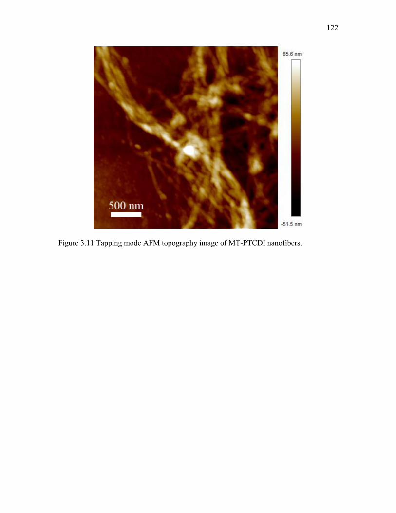
122
Figure 3.11 Tapping mode AFM topography image of MT-PTCDI nanofibers.

123
5 10 15 20 25 30 10 15 20 25 30
Inte
ns
ity
(a
.u.)
2Theta (degree)
010 (18.10 Å)
001 (25.38 Å)
(27.35 Å)
(22.25 Å)
(21.08 Å)
(40.71 Å)
(23.43 Å)
(b)(a)
05
0 (
3.6
9 Å
)
(4.3
3 Å
) (4
.15
Å)
(4.6
1 Å
)
Inte
ns
ity
(a
.u.)
2Theta (degree)
MP-PTCDI
MT-PTCDI
MA-PTCDI
MO-PTCDI
DD-PTCDI
CH-PTCDI
00
2 (
10
.47
Å)
9.3
6 Å
9
.17
Å
10
0 (
7.1
5 Å
)
00
4 (
5.2
7 Å
)
(5.1
5 Å
)
00
2 (
12
.50
Å)
00
3 (
8.1
8 Å
)
(7.1
9 Å
)
(6.8
9 Å
)
00
4 (
6.0
9 Å
)
00
6 (
4.3
9 Å
)
00
7 (
3.8
0 Å
)
(14.77 Å) (8.76 Å)
(8.16 Å) (6.97 Å) (4.72 Å) (3.97 Å)
(14.07 Å)
(12.01 Å) (8.01 Å)
(4.7
1 Å
)
Figure 3.12 PTCDI nanofibers’ crystal structures: (a) XRD patterns of PTCDI nanofibers
studied in this work; (b) the full patterns ranging from 2θ = 5 to 30 degree. The XRD
peaks of DD-PTCDI and CH-PTCDI nanofibers are in good agreement with the previous
reports,29,37,38 and can be indexed accordingly as marked in the figures. Since the single
crystal structures of the other PTCDI materials (MP-PTCDI, MT-PTCDI, MA-PTCDI
and MO-PTCDI) are unknown, we can’t fully index the peaks, but the d-spacing values
were calculated and labeled in the figures.

124
Figure 3.13 Evidences of photoinduced charge separation within the MP-PTCDI
nanofibers: (a) tapping mode AFM topography image of MP-PTCDI nanofibers; surface
potential images of the same area in panel a before (b) and after (d) illumination. The
statistics distribution of the relative surface potential before (c) and after illumination (e).

125
Figure 3.14 Study of MT-PTCDI solution in chloroform: (a) normalized UV-vis
absorption (black) and fluorescence (red) spectra of MT-PTCDI solution in chloroform (2
μmol L1). The excitation wavelength for the fluorescence spectrum was 490 nm; (b) day
light and fluorescence photographs (365 nm excitation) of 2 μmol L1 solution of MT-
PTCDI in chloroform.

126
Figure 3.15 Morphology, UV-vis absorption, and fluorescence emission of MT-PTCDI
thin film: (a, b) bright-field and fluorescence optical microscopy images of MT-PTCDI
nanofibers deposited on a quartz slide; (c) UV-vis absorption (black) and fluorescence
(red) spectra of MT-PTCDI nanofibers. The excitation wavelength for the fluorescence
spectrum was 510 nm.

127
0 1000 2000 3000
0.0
0.2
0.4
0.6
0.8
1.0
2.8 3.2 3.6 4.03.0
3.5
4.0
4.5
5.0
5.5(b)
No
rma
lize
d c
urr
en
t
Time (s)
298 K
323 K
343 K
363 K
(a)
ln ( P
PC)
(s)
1000/T (1/K)
Figure 3.16 Temperature dependent PPC decay of MP-PTCDI nanofibers: (a) PPC decay
curves of MP-PTCDI nanofibers measured at different temperatures; (b) logarithmic plot
of the decay time constant as a function of reciprocal of temperature. The illumination
power density was 3.50 mW cm2, and the bias voltage was 7 V.
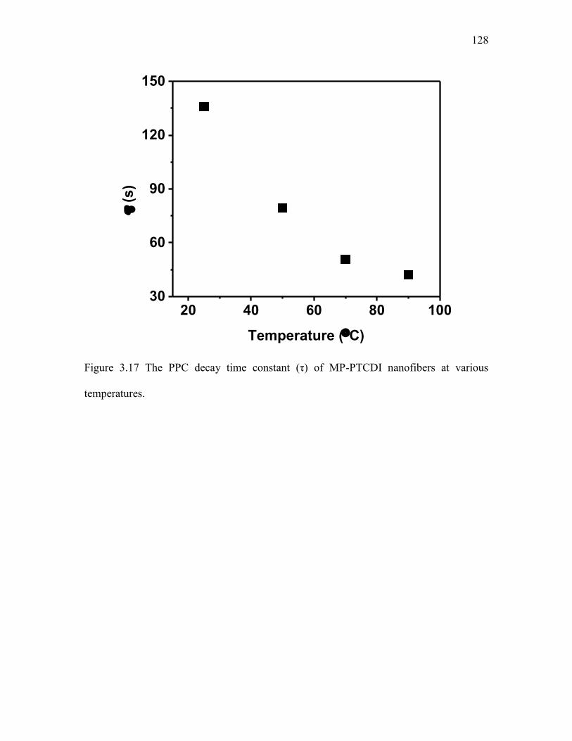
128
Figure 3.17 The PPC decay time constant (τ) of MP-PTCDI nanofibers at various
temperatures.
20 40 60 80 10030
60
90
120
150
(s
)
Temperature (C)

129
Table 3.1 The photocurrent on/off ratio, decay time constant of MP-PTCDI nanofibers,
and photocurrent equilibrium time under illumination with various power densities.
Irradiation power
density
(mW cm2)
Photocurrent on/off
ratio
Decay time constant
(τ, s)
Photocurrent
equilibrium time
(s)
0.31 18 1058 >500
0.76 29 389 >500
1.90 39 174 >500
3.50 55 103 400
5.77 71 48 200

CHAPTER 4
THERMOACTIVATED ELECTRICAL CONDUCTIVITY
IN PERYLENE DIIMIDE NANOFIBER MATERIALS1
4.1 Abstract
Thermoactivated electrical conductivity has been studied on nanofibers fabricated
from the derivatives of perylene tetracarboxylic diimide (PTCDI) both in the dark and
under visible light illumination. The activation energy obtained for the nanofibers
fabricated from donor−acceptor (D−A) PTCDIs are higher than that for symmetric n-
dodecyl substituted PTCDI. Such difference originates from the strong dependence of
thermoactivated charge hopping on material disorder, which herein is dominated by the
D−A charge-transfer and dipole−dipole interactions between stacked molecules. When
the nanofibers were heated above the first phase transition temperature (around 85 °C),
the activation energy was significantly increased because of the thermally enhanced
polaronic effect. Moreover, charge carrier density can be increased in the D−A nanofibers
under visible light illumination. Consistent with the theoretical models in the literature,
1 Reprinted with permission from Wu, N.; Zhang, Y.; Wang, C.; Slattum, P. M.; Yang,
X.; Zang, L., Thermo-activated Electrical Conductivity in Perylene Diimide Nanofiber
Materials. J. Phys. Chem. Lett. 2017, 8, 292-298. Copyright © 2016 American Chemical
Society.

131
the increased charge carrier density did cause decrease in the activation energy due to the
up-shifting of Fermi level closer to the conduction band edge.
4.2 Introduction
Organic semiconductor materials have drawn increasing attention in both
fundamental and application research, mainly because of the unique features of these
materials in comparison to those of conventional inorganic counterparts.1-4 The typical
features include structure and property flexibility through molecular design and
engineering, low temperature solution processability, and mechanical conformity to
different shapes of substrate. Organic semiconductors have been employed in a wide
variety of electronic and optoelectronic devices, such as transistors, diodes, sensors, solar
cells, and light-emitting devices. The operation performance of these device systems is
usually highly concerned with the electrical conductivity (or the charge transport) within
the materials. Although the electrical conductivity of the organic semiconductor is
primarily determined by the intrinsic structure (e.g., molecular structure, intermolecular
arrangement), some extrinsic physical parameters like temperature can also cause
significant modulation in the conductivity through changing the carrier mobility via the
so-called thermoactivated process. With this sensitive temperature dependence, some
organic materials have been developed into temperature sensors,5-7 which are suited for
integration into wearable systems for in situ monitoring of human activity and personal
healthcare.8-10
In general, the charge transport in organic materials relies on hopping between the
localized energy states (trapped charges),11-13 which can typically be described as a

132
thermoactivated process. Higher temperatures facilitate transport by providing the
thermo-energy required to overcome the energetic barriers created by disorders.
Arrhenius fitting of the conductivity as a function of temperature gives estimation of the
activation energy. For many organic semiconductors (including conducting polymers),
the activation energy was determined in the range of tens to hundreds of
millielectronvolts.13-15 The origin of the activation energy can be attributed to two major
contributions, energetic disorder and polaronic effect.13,16 The former is usually referred
to the diagonal disorder, which is referred to the fluctuations in molecular electronic
energies as arranged within the material. Such energetic disorder is commonly described
as Gaussian distribution of the molecular electronic energies [mostly the highest occupied
molecular orbital (HOMO) and lowest unoccupied molecular orbital (LUMO) level
energies], which is usually referred as Gaussian disorder model (GDM).16 While the
diagonal disorder is mainly contributed by the conformational freedom of component
molecules, it can also be induced by electrostatic or polarization effects from surrounding
molecules, particularly when the molecules contain significant dipole moments (e.g., the
electron donor-acceptor structure).17,18 The polaron effect in organic materials is mainly
due to molecular distortion caused by charging and decharging a molecule with an
electron.16,19,20 Hopping of an electron in this case is associated with both intramolecular
and intermolecular reorganization in solid stacks. It is evidenced that the polaron effect
can become more significant at elevated temperature because of the increased molecular
vibration.16
Description of charge transport considers both the charge hopping rates between the
localized sites and the density of charges involved in the hopping. Some well-established

133
models, such as the Miller-Abrahams model and that based on Marcus theory, have been
developed to describe the hopping rate in disordered organic materials. With the varying
densities of charges (e.g., modulated by gate voltage in field-effect transistors, or
chemical doping through electron donor or acceptor modification), these theoretical
models have been successfully applied in interpreting the observed temperature
dependence of electrical conductivity of different organic materials. However, most of
these studies were performed on the conducting polymers like those based on poly-
phenylenevinylene (PPV) and poly(3-hexylthiophene) (P3HT), or the intrinsic (n- or p-
type) molecular semiconductor materials such as the crystals of pentacene, rubrene or
triphenylene.13 We report therein on the temperature activated charge transport within
self-doped organic semiconductors, which were assembled from the covalently linked
electron donor-acceptor (DA) molecules based on the derivatives of perylene
tetracarboxylic diimide (PTCDI, Figure 4.1). As a unique air-stable n-type organic
semiconductor, PTCDIs have been explored for various electrical or optical applications
such as photovoltaics, light-emitting diodes, and photoelectric sensors.1,21-23 More
importantly, PTCDI materials offer robust thermal stability with decomposition
temperature around 400 C or above,24 thus enabling investigation of thermoactivation in
a wide high-temperature range.
DA molecular materials provide increased electrical conductivity through the
charge-transfer interaction between the donor and acceptor moieties, which in turn results
in increase in charge carrier density.1,25-27 Because of the effective self-doping, DA
materials have been widely employed in electronic and optoelectronic systems or devices,
particularly photovoltaics. Despite the gain of increased conductivity, the D-A charge

134
transfer creates structural disorder and/or polaronic effect, which combined lead to
increased energetic barrier for the charge hopping, meaning higher temperature will be
needed to activate the charge transport. It therefore becomes imperative to study the
temperature dependent charge transport of these materials. Moreover, most of the D-A
materials are also photoconductive, i.e., light illumination of these materials initiates the
electron transfer from D to A moiety, and further charge separation leads to increase in
charge carrier density.27 Increasing carrier density will shift up the Fermi level to the
conduction band, resulting in decease in thermoactivation energy for the charge hopping,
for which the activation barrier is generally considered as the energy difference between
the trapped state and conduction band.28,29 In this regard, the photoconductive feature of
D-A materials provides an alternative way to study the thermoactivated charge transport
by changing the carrier density, in a manner similar to that of the studies employing field-
effect transistors (FET), wherein the charge carrier density can be modulated by the gate
voltage.
4.3 Experimental Section
4.3.1 Synthesis of PTCDI Molecules and Fabrication of Nanofibers
The DD-PTCDI molecule was synthesized as the previously reported method.30 BN-
PTCDI and BNO-PTCDI molecules were synthesized following a similar procedure for
asymmetric PTCDI molecules.25,31 First, N-dodecyl-perylene-3,4,9,10-tetracarboxy
monoimide monoanhydride compound was synthesized using the previously reported
method.25,31 Second, monoimide monoanhydride compound (490 mg), (4-
piperidinophenyl)methylamine (500 mg, Sigma-Aldrich), Zn(CO2CH3)2 (8 mg, Sigma-

135
Aldrich, ACS reagent, 98%) and imidazole (4.5 g, Sigma-Aldrich, ACS reagent, > 99%)
were added into a 20 mL vial. The reaction mixture was stirred with a magnetic stir bar at
150 °C for 4 h. After cooling to room temperature, the above mixture was poured into 2N
HCl to dissolve the imidazole. The remained product was collected by filtration and
washed with distilled water and methanol. The resulting product was dispersed in
chloroform (200 mL) and washed with saturated sodium bicarbonate, water, brine and
dried over Na2SO4, followed by purified on a silica column eluting with 1.5 % ethanol in
chloroform to yield 268 mg product. 1H NMR (400 MHz, CDCl3, ppm): δ = 8.84 (d, J =
8.0 Hz, 4H; perylene H), 8.81 (d, J = 8.0 Hz, 4H, perylene H), 7.73 (d, J = 8.4 Hz, 2H;
benzene H), 7.47 (d, J = 8.4 Hz, 2H; benzene H), 5.52 (s, 2H; (CO)2NCH*2(C6H4)),
4.274.24 (m, 2H, (CO)2NCH*2(CH2)10), 3.783.61 (m, 4H; C6H4N(CH*2)2), 2.071.26
(m, 26H; CH2), 0.86 (t, J = 6.8 Hz, 3H; CH3). MALDI-TOF-MS: [M+H+]/z = 732.43.
BNO-PTCDI molecule was synthesized as the same method as BN-PTCDI, except
the corresponding amine of functional moiety was used and the amount of reactants were
changed. For the synthesis of BNO-PTCDI, [4-(morpholin-4-yl)phenyl]methanamine
(359 mg, Sigma-Aldrich) was used as the substitution reactant. The amount of the other
reactants was 300 mg (monoimide monoanhydride), 5 mg (Zn(CO2CH3)2) and 4.5 g
(imidazole). The final product of BNO-PTCDI was 268 mg. 1H NMR (400 MHz, CDCl3,
ppm): δ = 8.83 (d, J = 8.0 Hz, 4H; perylene H), 8.79 (d, J = 8.4 Hz, 4H, perylene H), 7.75
(d, J = 8.4 Hz, 2H; benzene H), 7.53 (d, J = 8.4 Hz, 2H; benzene H), 5.52 (s, 2H;
(CO)2NCH*2(C6H4)), 4.264.23 (m, 6H, (CO)2NCH*2(CH2)10, C6H4N(CH*2)2), 3.77 (m,
4H; C6H4N(CH2)2(CH*2)2O), 1.761.26 (m, 20H; CH2), 0.87 (t, J = 6.8, 3H; CH3).
MALDI-TOF-MS: [M+H+]/z = 734.33.

136
In this work, PTCDI molecules were self-assembled into nanofibers through a solvent
exchange processing.30 Typically, 1 mL of PTCDI solution in chloroform (0.1 mmol L1)
was injected into 5 mL ethanol. The mixture was aged in the dark over night to facilitate
the precipitation of the fibrous materials.
4.3.2 Materials Characterization
X-ray diffraction patterns of PTCDI nanofiber thin films were obtained using a
Bruker D2 Phase X-ray diffractometer with Cu Kα (λ = 1.5418 Å). The thin films for
XRD measurement were prepared by drop-casting PTCDI nanofibers into a clean glass
slide substrate (D = 1.5 cm). Differential scanning calorimetry (DSC) measurements were
conducted by a NETZSCH DSC 3500 calorimeter with a heating/cooling rate of 10 °C
min1. Two heating-cooling cycles were performed for each sample. UV−vis absorption
spectra were recorded with an Agilent Cary 100 UV-vis spectrophotometer. Fluorescence
spectra were collected on an Agilent Eclipse spectrophotometer. The bright field and
fluorescence optical images were obtained with a Leica DMI4000B inverted microscope
equipped with an Acton SP-2356 Imaging Spectrograph system and Princeton Instrument
Acton PIXIS: 400B Digital CCD Camera System for high resolution imaging. Atomic
force microscopy (AFM) measurements were performed on a Veeco MultiMode V
scanning probe microscope in tapping mode. Samples for AFM measurements were made
by depositing PTCDI nanofibers on a silicon substrate coated with a polished 300 nm
thick SiO2 layer (Silicon Quest International), and drying in vacuum oven at room
temperature in dark.

137
4.3.3 Temperature-Dependent Electrical Current Measurement
Interdigitated electrodes (IDEs) were used for all electrical current measurements.
The IDEs were fabricated by a standard photolithography procedure on a silicon wafer
with a 300 nm thermal oxide layer (Silicon Quest International). The electrodes were
made by sputtering with 20 nm titanium adhesion layer and 50 nm gold layer. The IDE
channel width and gap length was 1150 μm and 20 μm, respectively. The electrical
conductivity was measured using a two-probe method on a Signatone S-1160 Probe
Station combined with an Agilent 4156C Precision Semiconductor Analyzer. All the
current measurements were under a bias voltage of 10 V. In the photocurrent
measurement, the white light was supplied by a tungsten lamp (Quartzline, 21 V, 150 W)
through a glass optical fiber. An objective lens was used to focus the light on the sample
to insure the whole nanofiber thin film was covered by light. The optical power reaching
the sample surface was measured by a power meter (Mells Griot broadband power/energy
meter, 13PEM001). For the temperature-dependent current test, the IDE was placed on a
hot stage connected with a temperature controller (INSTEC, STC 200). The temperature
was increased from 25 to 120 °C with a rate of 2 °C min1. A layer of thermal paste
(Arctic Sliver 5) was applied between the IDEs and the heating stage to improve the
thermal transfer. The temperature change due to the white light irradiation is negligible.
4.4 Results and Discussion
The PTCDI D-A materials used in this study are in the nanofiber morphology (Figure
4.2), which are fabricated by solution self-assembly of the DA molecules, BN-PTCDI
and BNO-PTCDI. The one-dimensional (1D) morphology is dominated by the

138
stacking of the planar PTCDI molecules, and the 1D molecular stacking facilitates the
charge separation between the photogenerated electron and hole through the
intermolecular -electron delocalization.27 The further increased charge density is
conducive to studying the thermoactivated charge transport, for which the activation
energy is related to the charge density as evidenced in the FET studies. Although PTCDI
nanofiber materials have been extensively studied and used in varying applications (e.g.,
photovoltaics, sensors), there is little study reported yet on the temperature-dependent
charge transport or electrical conductivity. The presented work would fill in this research
gap, by providing improved understanding of the thermoactivated charge transport, and
the observation may furthermore lead to development of wearable temperature sensors,
taking advantages of the flexibility and small size of the nanofibers.
Along with the two DA molecules, BN-PTCDI and BNO-PTCDI (Figure 4.1), a
normal PTCDI molecule (without substitution of D moiety), DD-PTCDI, was also
employed as a control in this study to investigate the effect of DA structure and the
photoinduced charge separation on the thermoactivated charge transport. While DD-
PTCDI was synthesized following the same method previously reported,30 BN-PTCDI
and BNO-PTCDI were synthesized using a modified procedure as detailed in the
Experimental Section. As expected, these PTCDI molecules form well-defined
nanofibers when self-assembled in solutions (Figure 4.2a-c), mainly dictated by the
strong ππ stacking interaction in between. All the nanofibers are in high aspect ratio
with length in the range of a few tens of micrometers. The average width of the
nanofibers, as estimated by atomic force microscopy (AFM) imaging, is ca. 263, 213 and
200 nm for BN-PTCDI, BNO-PTCDI and DD-PTCDI, respectively. These nanofibers
139
were then deposited onto interdigitated electrodes (IDEs) for electrical measurement and
characterization (Figure 4.2d).
For all the three PTCDI nanofibers, the electrical current measured under the same
conditions (as illustrated in Figure 4.2d) showed significant increase with temperature
when heated from 25 to 120 °C (Figure 4.3). One typical heatingcooling cycle, as
monitored over the BN-PTCDI nanofibers, is shown in Figure 4.4. The temperature
responses observed were completely reversible, indicating the structure robustness of
PTCDI materials under heating. Such robust repeatability assures the feasibility of
applying these materials in temperature sensors in future. Among the three nanofibers,
BN-PTCDI demonstrated the most sensitive response to temperature both in the dark and
under white light illumination which creates photoconductivity as indicated by the much
increased current. With the temperature increased from 25 to 120 °C, the current
increased by a factor of 1350, 342 and 19 in the dark (Figure 4.3a) and 273, 67 and 17
under illumination (Figure 4.3b) for BN-PTCDI, BNO-PTCDI and DD-PTCDI,
respectively. Under both dark and illuminated conditions, the relative increase of current
with temperature of BNO-PTCDI is significantly smaller than that of BN-PTCDI, but is
still much larger than that of DD-PTCDI. The more sensitive temperature dependence of
current means higher energy barrier for the thermoactivated charge transport, and this can
be seen more clearly from the activation energy, which can in turn be estimated from the
linear fitting of the data in Figure 4.3 using the Arrhenius equation (Equation 4.1),13,16
𝐼 = 𝐼0𝑒−𝐸𝐴𝑘𝑇 4.1

140
where I is the electrical current measured under temperature T; k the Boltzmann constant;
EA the activation energy; and 𝐼0 is the current when EA is ignored, i.e., in the case of free
charge transport. As shown in Figure 4.5, good linear fitting can be obtained for the data
either in the low- (2580 °C) or high-temperature range (80120 °C) with a turning point
around 80 °C, but not in the whole temperature range of experiment. The slope of the
linear fitting gives the activation energiers, EA, which are summarized in Table 4.1 for
comparison between the three nanofibers. The two linear ranges may indicate two
different phases of the material, which would be characteristic with different activation
energy. Remarkably, the turning temperature indicated in Figure 4.5 (80 °C) is highly
consistent with the result of DSC, wherein one phase transition temperature of 85 °C was
observed for DD-PTCDI. For both the dark current and photocurrent measurements,
larger activation energy was observed in the higher-temperature range for all the three
nanofibers, implying that some additional contribution to the thermoactivation barrier
was generated by increasing temperature. We attribute this additional contribution to the
heating-enhanced intermolecular disorder, which in turn may also enhance the polaronic
effect. As indeed indicated by the theoretical modeling,16 at sufficiently high temperature
(depending on materials) the polaronic effect can become more dominant than the
energetic disorder in controlling the charge transport.
The activation energies shown in Table 4.1, particularly those obtained in low
temperature range, are in good consistency with the values measured for the other organic
semiconductors under the similar temperatures using the FET devices under varying
temperatures.13,14,32 Also in the lower-temperature range, the activation energies of the
two DA PTCDIs, BN-PTCDI and BNO-PTCDI, are much higher than that of DD-

141
PTCDI which contains no donor moiety. This can be explained by the much increased
disorder within the DA materials, wherein intermolecular DA interaction (concerted
with the strong dipole-dipole interaction) would distort the molecular arrangement,
creating traps for the charge carriers. In contrast, the DD-PTCDI material is mostly
controlled by the stacking, for which there is little disorder contribution from the
dipoledipole interaction, considering the close to zero dipole moment of the symmetric
molecule. When comparisons are made between BN-PTCDI and BNO-PTCDI in the low
temperature range, the activation energy of the former is significantly higher than the
latter, ca. 1.35 and 1.77 times for the dark current and photocurrent measurement,
respectively. The higher activation energy of BN-PTCDI is apparently due to the
stronger DA interaction between the phenylpiperidine group and PTCDI in comparison
to that between phenylmorpholine and PTCDI in BNO-PTCDI material. Indeed, as
indicated by our density-functional theory calculation (Figure 4.6), the electron donating
power (determined by the HOMO level) of phenylpiperidine is 0.13 eV stronger than that
of phenylmorpholine. It is interesting to note that with temperature increasing to
sufficiently high levels (here around 80 °C), the relative difference in activation energy
between the three nanofibers becomes much smaller than that observed in the low
temperature range. This implies that the thermally induced molecular disorder (e.g.,
conformational defects) at elevated temperature may override the effects of DA or
dipoledipole interaction, which are usually dominant at low temperatures.
The enhanced low-temperature disorder of the two DA PTCDI materials (compared
to DD-PTCDI) as discussed above was also supported by the X-ray diffraction (XRD)
and differential scanning calorimetry (DSC) measurements (Figure 4.7 and Figure 4.8).

142
Figure 4.7 shows the XRD patterns measured for BN-PTCDI, BNO-PTCDI and DD-
PTCDI nanofibers. For DD-PTCDI nanofibers, well-defined XRD peaks are observed
and can be indexed from (001) to (007), which are consistent with the previous reports on
the same fiber materials (though fabricated with slightly different self-assembly
procedures).30,33,34 The d-spacing of 25.38 Å (deduced from the primary peak at 3.49°)
corresponds to the intercolumnar distance, which is about half of the length of two DD-
PTCDI molecules tail-to-tail interdigitated.31,35 The 23.37° peak is indexed as the co-
facial stacking between two PTCDI planes, and the calculated stack spacing (3.80 Å) is
consistent with the typical π-π stacking distance as observed for other planar π-
conjugated molecules.31,34 To minimize the free energy caused by π-π electronic
repulsion, a transverse and/or longitudinal offset is usually observed between the stacked
PTCDI planes, resulting in a different edge-to-edge distance from the π-π stacking
distance.36 The d-spacing of 4.39 Å (calculated from the peak 20.21°) corresponds to the
edge-to-edge distance between the two stacked DD-PTCDI planes, which take a tilted
packing conformation. In contrast to the high-quality crystalline structure observed for
DD-PTCDI, the structures of BN-PTCDI and BNO-PTCDI look less organized as
indicated by the XRD patterns in Figure 4.7. The XRD peak intensity measured for the
nanofibers of BN-PTCDI and BNO-PTCDI decreased by about 1 order of magnitude in
comparison to that of DD-PTCDI nanofibers. Nonetheless, the intercolumnar spacings,
23.49 and 22.89 Å, as calculated for BN-PTCDI and BNO-PTCDI from the primary
diffraction peaks, are quite close to the spacing value (25.38 Å) obtained for DD-PTCDI,
indicating a similar cofacial π-π stacking arrangement drives the 1D growth of nanofibers
in all the three PTCDIs.

143
Consistent with the XRD measurement, the DSC result also suggests less ordered
structure for the two D-A PTCDI materials compared to DD-PTCDI. DSC is a common
method used for studying the phase transition of molecular materials, including the
PTCDIs.30,37,38. As shown in Figure 4.8, upon heating, DD-PTCDI nanofibers
demonstrated three crystalline-crystalline transitions occurred at 85, 160 and 175 °C prior
to the melting transition (Tm > 200 °C). When the sample was cooled, a dominant
transition from mesophase to crystallization was observed at about 153 °C. Unlike DD-
PTCDI, BN-PTCDI and BNO-PTCDI did not exhibit a clear phase transition upon
heating, though during the cooling cycle a broad, asymmetric peak can be observed
around 172 and 153 °C for BN-PTCDI and BNO-PTCDI, respectively, implying the
transition from mesophase to crystallization phase. This observation suggests more
disorder structure of the D-A PTCDIs compared to the highly organized molecular
packing within DD-PTCDI. The high-quality crystalline structure of DD-PTCDI is
mostly due to the symmetric molecular geometry substituted by two linear alkyl chains.
This type of PTCDIs is conducive to forming organized columnar stacks in a manner
similar to that of liquid crystal.38 As discussed above, structure disorder leads to
increased activation energy for charge transport, which is evidenced in our electrical
current measurements shown in Figure 4.3 and Figure 4.5. Such disorder-dependent
thermoactivation was also observed previously by others in pentacene thin-film
transistors,15 for which the films morphologies could be tuned and optimized by
deposition of the film on a substrate at varying temperatures. Depending on the
deposition temperature, different quality of films can be obtained, and low-temperature
deposition usually led to low-quality film with more deep level traps, which in turn

144
resulted in large activation energy.
It is also interesting to be seen from Table 4.1 (Figure 4.5 as well) that the activation
energy obtained particularly in the D-A PTCDI nanofibers was significantly decreased
when measured under white light illumination in comparison to that in the dark. This
decrease in activation energy is likely due to the increase in charge carrier density
resulting from the photoinduced charge separation within the nanofibers. An increase in
charge carrier density (here electrons for PTCDI) shifts up the Fermi level through the
trap distribution, closer to the conduction band edge, and as a result, the thermal energy
required to activate the trapped charge into hopping would be decreased. Such charge
carrier density dependence of thermoactivation was evidenced or implied in other studies,
both experimentally and theoretically, using the gate voltage to modulate the charge
carrier density.28,29
The increase in charge carrier density upon illumination can be clearly seen from the
dramatic increase in photocurrent compared to the dark current (Figure 4.3a, b). Indeed,
the electrical current of the two D-A nanofibers, BN-PTCDI and BNO-PTCDI, was
increased by more than 2 orders of magnitude when illuminated by white light. Such
dramatic photoconductive enhancement is largely due to the photoinduced charge
separation between the D moiety and PTCDI -conjugated backbone (the A part), which
produces increased density of charges.27,31,39 The photocurrent response observed for
DD-PTCDI under the same illumination condition was about 1 order of magnitude lower
than that of the D-A PTCDIs, likely due to the lack of electron-donating groups. The
photoinduced electron transfer from the D moieties to PTCDI is very thermodynamically
favorable with a driving force of 0.74 and 0.61 eV for BN-PTCDI and BNO-PTCDI,

145
respectively (Figure 4.6). The transferred electron will be delocalized along the
stacks of PTCDIs, further enhancing the charge separation.27 The photoinduced
intramolecular electron transfer within the two D-A molecules was also evidenced by the
efficient fluorescence quenching in both solutions and solid state (Figure 4.9 and Figure
4.10). As shown in Figure 4.9, the BN-PTCDI and BNO-PTCDI molecules dissolved in
chloroform exhibit very weak fluorescence emission, whereas DD-PTCDI demonstrated
strong fluorescence under the same conditions. The dramatic fluorescence quenching is
due to the efficient photoinduced intramolecular electron transfer from the D moiety to
PTCDI (as illustrated in Figure 4.6). Similar fluorescence quenching has been observed
within many other D-A molecules, including the PTCDIs substituted with different
amines.31,40 To further confirm the intramolecular electron transfer, hydrochloric acid was
added into the solution of BN-PTCDI or BNO-PTCDI to protonate the amines, in order
to lower the energy level of the lone electron pair, thus blocking the photoinduced
intramolecular electron transfer as evidenced before in numerous D-A molecular
systems.31,40 Indeed, the addition of hydrochloric acid resulted in strong fluorescence
turning on as shown in Figure 4.9. Similarly, the significant fluorescence quenching was
also observed in the solid state of BN-PTCDI and BNO-PTCDI nanofibers, whereas DD-
PTCDI nanofibers remained strong fluorescent (Figure 4.10).
4.5 Conclusions
In conclusion, we have investigated the temperature dependent charge transport
(measured as electrical current) for three PTCDI nanofibers with two in D-A structure
(BN-PTCDI and BNO-PTCDI), and the third one without strong donor substitution (DD-

146
PTCDI). The results support the thermoactivated hopping mechanism for the charge
transport, for which the activation energy was found to be primarily dependent on D-A
structure. Indeed, both the D-A nanofibers showed activation energy that was
significantly higher than that of the DD-PTCDI nanofibers for both the dark current and
photocurrent measurements. D-A structure helps create disorder regarding both the
charge-transfer and dipole-dipole interactions between stacked molecules, and the
increased disorder enlarges the activation barrier. Significant increase in activation
energy was found when heating the materials above the first crystallization to
crystallization transition temperature, and this is likely due to the heating-enhanced
intermolecular disorder, with which the polaronic effect may become more dominant in
controlling the charge hopping process. Under visible light illumination, the electrical
current of the nanofibers can be increased by orders of magnitude, thus providing the
opportunity to examine the effect of charge carrier density on the activation energy of
thermoactivated charge transport. As expected from the theoretical modeling in
literature, the increased charge carrier density caused decrease in the activation energy
because of the up-shifting of Fermi level through the energetic trap distribution in the
bandgap. The photocurrent measurement offers an alternative way, in addition to the
gate control in FET device, to modulate the charge density in material and investigate the
effect on the thermoactivation of charge hopping. This work also reveals a trade-off
regarding the design rules of D-A molecular materials. On one hand, D-A structure
enables charge transfer and separation, particularly under light illumination, producing
high conductivity, but on the other hand, the D-A materials are often more disordered
compared to the neutral (low dipole) materials, thus resulting in higher activation energy

147
for charge transport. This may be conducive to developing more sensitive temperature
sensors, but for many other electronic systems or applications more organized materials
are usually required, which in turn demands more control of the intermolecular
arrangement through molecular structural design and engineering.
4.6 References
(1) Hains, A. W.; Liang, Z.; Woodhouse, M. A.; Gregg, B. A. Molecular
Semiconductors in Organic Photovoltaic Cells. Chem. Rev. 2010, 110, 6689-6735.
(2) Coakley, K. M.; McGehee, M. D. Conjugated Polymer Photovoltaic Cells. Chem.
Mater. 2004, 16, 4533-4542.
(3) Samuel, I. D. W.; Turnbull, G. A. Organic Semiconductor Lasers. Chem. Rev. 2007,
107, 1272-1295.
(4) Sirringhaus, H. Organic Semiconductors: An Equal-Opportunity Conductor. Nat.
Mater. 2003, 2, 641-642.
(5) Jung, S.; Ji, T.; Varadan, V. K. Temperature Sensor Using Thermal Transport
Properties in the Subthreshold Regime of an Organic Thin Film Transistor. Appl. Phys.
Lett. 2007, 90, 062105.
(6) Ren, X.; Chan, P. K. L.; Lu, J.; Huang, B.; Leung, D. C. W. High Dynamic Range
Organic Temperature Sensor. Adv. Mater. 2013, 25, 1291-1295.
(7) Trung, T. Q.; Ramasundaram, S.; Hong, S. W.; Lee, N.-E. Flexible and Transparent
Nanocomposite of Reduced Graphene Oxide and P(VDF-TrFE) Copolymer for High
Thermal Responsivity in a Field-Effect Transistor. Adv. Funct. Mater. 2014, 24, 3438-
3445.
(8) Trung, T. Q.; Lee, N.-E. Flexible and Stretchable Physical Sensor Integrated
Platforms for Wearable Human-Activity Monitoringand Personal Healthcare. Adv. Mater.
2016, 28, 4338-4372.
(9) Chortos, A.; Liu, J.; Bao, Z. Pursuing Prosthetic Electronic Skin. Nat. Mater. 2016,
15, 937-950.
(10) Someya, T.; Kato, Y.; Sekitani, T.; Iba, S.; Noguchi, Y.; Murase, Y.; Kawaguchi,
H.; Sakurai, T. Conformable, Flexible, Large-Area Networks of Pressure and Thermal
Sensors With Organic Transistor Active Matrixes. Proc. Natl. Acad. Sci. U. S. A. 2005,
102, 12321-12325.

148
(11) Lu, N.; Li, L.; Banerjee, W.; Sun, P.; Gao, N.; Liu, M. Charge Carrier Hopping
Transport Based on Marcus Theory and Variable-Range Hopping Theory in Organic
Semiconductors. J. Appl. Phys. 2015, 118, 045701.
(12) Tessler, N.; Preezant, Y.; Rappaport, N.; Roichman, Y. Charge Transport in
Disordered Organic Materials and Its Relevance to Thin-Film Devices: A Tutorial
Review. Adv. Mater. 2009, 21, 2741-2761.
(13) Coropceanu, V.; Cornil, J.; da Silva Filho, D. A.; Olivier, Y.; Silbey, R.; Brédas, J.-
L. Charge Transport in Organic Semiconductors. Chem. Rev. 2007, 107, 926-952.
(14) Horowitz, G.; Hajlaoui, M. E.; Hajlaoui, R. Temperature and Gate Voltage
Dependence of Hole Mobility in Polycrystalline Oligothiophene Thin Film Transistors. J.
Appl. Phys. 2000, 87, 4456-4463.
(15) Knipp, D.; Street, R. A.; Völkel, A. R. Morphology and Electronic Transport of
Polycrystalline Pentacene Thin-Film Transistors. Appl. Phys. Lett. 2003, 82, 3907-3909.
(16) Fishchuk, I. I.; Kadashchuk, A.; Hoffmann, S. T.; Athanasopoulos, S.; Genoe, J.;
Bässler, H.; Köhler, A. Unified Description for Hopping Transport in Organic
Semiconductors Including Both Energetic Disorder and Polaronic Contributions. Phys.
Rev. B: Condens. Matter Mater. Phys. 2013, 88, 125202.
(17) Dieckmann, A.; Bässler, H.; Borsenberger, P. M. An Assessment of the Role of
Dipoles on the Density‐of‐States Function of Disordered Molecular Solids. J. Chem.
Phys. 1993, 99, 8136-8141.
(18) Dunlap, D. H.; Parris, P. E.; Kenkre, V. M. Charge-Dipole Model for the Universal
Field Dependence of Mobilities in Molecularly Doped Polymers. Phys. Rev. Lett. 1996,
77, 542-545.
(19) Chang, J.-F.; Sirringhaus, H.; Giles, M.; Heeney, M.; McCulloch, I. Relative
Importance of Polaron Activation and Disorder on Charge Transport in High-Mobility
Conjugated Polymer Field-Effect Transistors. Phys. Rev. B: Condens. Matter Mater.
Phys. 2007, 76, 205204.
(20) Parris, P. E.; Kenkre, V. M.; Dunlap, D. H. Nature of Charge Carriers in Disordered
Molecular Solids: Are Polarons Compatible With Observations? Phys. Rev. Lett. 2001,
87, 126601.
(21) Würthner, F.; Saha-Möller, C. R.; Fimmel, B.; Ogi, S.; Leowanawat, P.; Schmidt,
D. Perylene Bisimide Dye Assemblies as Archetype Functional Supramolecular
Materials. Chem. Rev. 2016, 116, 962-1052.
(22) Zang, L.; Che, Y.; Moore, J. S. One-Dimensional Self-Assembly of Planar π-
Conjugated Molecules: Adaptable Building Blocks for Organic Nanodevices. Acc. Chem.
Res. 2008, 41, 1596-1608.

149
(23) Chen, S.; Slattum, P.; Wang, C.; Zang, L. Self-Assembly of Perylene Imide
Molecules into 1D Nanostructures: Methods, Morphologies, and Applications. Chem.
Rev. 2015, 115, 11967-11998.
(24) Pasaogullari, N.; Icil, H.; Demuth, M. Symmetrical and Unsymmetrical Perylene
Diimides: Their Synthesis, Photophysical and Electrochemical Properties. Dyes Pigm.
2006, 69, 118-127.
(25) Wu, N.; Wang, C.; Bunes, B. R.; Zhang, Y.; Slattum, P. M.; Yang, X.; Zang, L.
Chemical Self-Doping of Organic Nanoribbons for High Conductivity and Potential
Application as Chemiresistive Sensor. ACS Appl. Mater. Interfaces 2016, 8, 12360-
12368.
(26) Huang, H.; Gross, D. E.; Yang, X.; Moore, J. S.; Zang, L. One-Step Surface Doping
of Organic Nanofibers to Achieve High Dark Conductivity and Chemiresistor Sensing of
Amines. ACS Appl. Mater. Interfaces 2013, 5, 7704-7708.
(27) Zang, L. Interfacial Donor–Acceptor Engineering of Nanofiber Materials to
Achieve Photoconductivity and Applications. Acc. Chem. Res. 2015, 48, 2705-2714.
(28) Chesterfield, R. J.; McKeen, J. C.; Newman, C. R.; Ewbank, P. C.; da Silva Filho,
D. A.; Brédas, J.-L.; Miller, L. L.; Mann, K. R.; Frisbie, C. D. Organic Thin Film
Transistors Based on n-Alkyl Perylene Diimides: Charge Transport Kinetics as a
Function of Gate Voltage and Temperature. J. Phys. Chem. B 2004, 108, 19281-19292.
(29) Fishchuk, I. I.; Kadashchuk, A. K.; Genoe, J.; Ullah, M.; Sitter, H.; Singh, T. B.;
Sariciftci, N. S.; Bässler, H. Temperature Dependence of the Charge Carrier Mobility in
Disordered Organic Semiconductors at Large Carrier Concentrations. Phys. Rev. B:
Condens. Matter Mater. Phys. 2010, 81, 045202.
(30) Balakrishnan, K.; Datar, A.; Naddo, T.; Huang, J.; Oitker, R.; Yen, M.; Zhao, J.;
Zang, L. Effect of Side-Chain Substituents on Self-Assembly of Perylene Diimide
Molecules: Morphology Control. J. Am. Chem. Soc. 2006, 128, 7390-7398.
(31) Che, Y.; Yang, X.; Liu, G.; Yu, C.; Ji, H.; Zuo, J.; Zhao, J.; Zang, L. Ultrathin n-
Type Organic Nanoribbons With High Photoconductivity and Application in
Optoelectronic Vapor Sensing of Explosives. J. Am. Chem. Soc. 2010, 132, 5743-5750.
(32) Knipp, D.; Street, R. A.; Völkel, A.; Ho, J. Pentacene Thin Film Transistors on
Inorganic Dielectrics: Morphology, Structural Properties, and Electronic Transport. J.
Appl. Phys. 2003, 93, 347-355.
(33) Huang, Y.; Fu, L.; Zou, W.; Zhang, F.; Wei, Z. Ammonia Sensory Properties Based
on Single-Crystalline Micro/Nanostructures of Perylenediimide Derivatives: Core-
Substituted Effect. J. Phys. Chem. C 2011, 115, 10399-10404.
(34) Jones, B. A.; Facchetti, A.; Wasielewski, M. R.; Marks, T. J. Tuning Orbital
Energetics in Arylene Diimide Semiconductors. Materials Design for Ambient Stability

150
of n-Type Charge Transport. J. Am. Chem. Soc. 2007, 129, 15259-15278.
(35) Bushey, M. L.; Hwang, A.; Stephens, P. W.; Nuckolls, C. Enforced Stacking in
Crowded Arenes. J. Am. Chem. Soc. 2001, 123, 8157-8158.
(36) Würthner, F. Perylene Bisimide Dyes as Versatile Building Blocks for Functional
Supramolecular Architectures. Chem. Commun. 2004, 1564-1579.
(37) Cormier, R. A.; Gregg, B. A. Synthesis and Characterization of Liquid Crystalline
Perylene Diimides. Chem. Mater. 1998, 10, 1309-1319.
(38) Struijk, C. W.; Sieval, A. B.; Dakhorst, J. E. J.; van Dijk, M.; Kimkes, P.; Koehorst,
R. B. M.; Donker, H.; Schaafsma, T. J.; Picken, S. J.; van de Craats, A. M.; et al. Liquid
Crystalline Perylene Diimides: Architecture and Charge Carrier Mobilities. J. Am. Chem.
Soc. 2000, 122, 11057-11066.
(39) Rühle, V.; Lukyanov, A.; May, F.; Schrader, M.; Vehoff, T.; Kirkpatrick, J.;
Baumeier, B.; Andrienko, D. Microscopic Simulations of Charge Transport in Disordered
Organic Semiconductors. J. Chem. Theory Comput. 2011, 7, 3335-3345.
(40) Zang, L.; Liu, R.; Holman, M. W.; Nguyen, K. T.; Adams, D. M. A Single-
Molecule Probe Based on Intramolecular Electron Transfer. J. Am. Chem. Soc. 2002,
124, 10640-10641.

151
Figure 4.1 Molecular structures of PTCDI derivatives studied in this work.

152
Figure 4.2 Tapping mode AFM topography images of (a) BN-PTCDI, (b) BNO-PTCDI
and (c) DD-PTCDI nanofibers; (d) schematic of the IDEs device and temperature control
system used for studying the thermo-activated charge transport of PTCDI nanofibers.

153
20 40 60 80 100 1201E-8
1E-7
1E-6
1E-5
1E-4
1E-3
0.01
0.1
20 40 60 80 100 120
1E-6
1E-5
1E-4
1E-3
0.01
0.1
1
10
Cu
rren
t (
A)
Temperature (C)
BN-PTCDI
BNO-PTCDI
DD-PTCDI
Dark current (b)
Cu
rren
t (
A)
Temperature (C)
BN-PTCDI
BNO-PTCDI
DD-PTCDI
(a)Photocurrent
Figure 4.3 The electrical current of PTCDI nanofibers measured at varying temperatures
in dark (a) and under white light illumination (7.5 mW cm-2) (b). A constant bias of 10 V
was applied during all the measurements. The dark current of BN-PTCDI is two orders of
magnitude higher than that of DD-PTCDI, and this is likely due to the self-doping by the
piperidine group, which is a strong electron donor and was used before for self-doping of
other PTCDIs to increase the electrical conductivity.25

154
Figure 4.4 Current profile of BN-PTCDI nanofibers in dark with temperature increasing
from 25 to 120 °C and then cooling to 25 °C. The bias voltage was 10 V.
0 2000 4000 6000 8000
0.00
0.01
0.02
0.03
0.04
0.05
Cu
rren
t (
A)
Time (s)
Tem
pera
ture
(C)
25
120
Heating Cooling

155
Figure 4.5 Arrhenius plot of current versus inverse temperature for PTCDI nanofibers in
dark (a) and under white light illumination (7.5 mW cm2) (b).
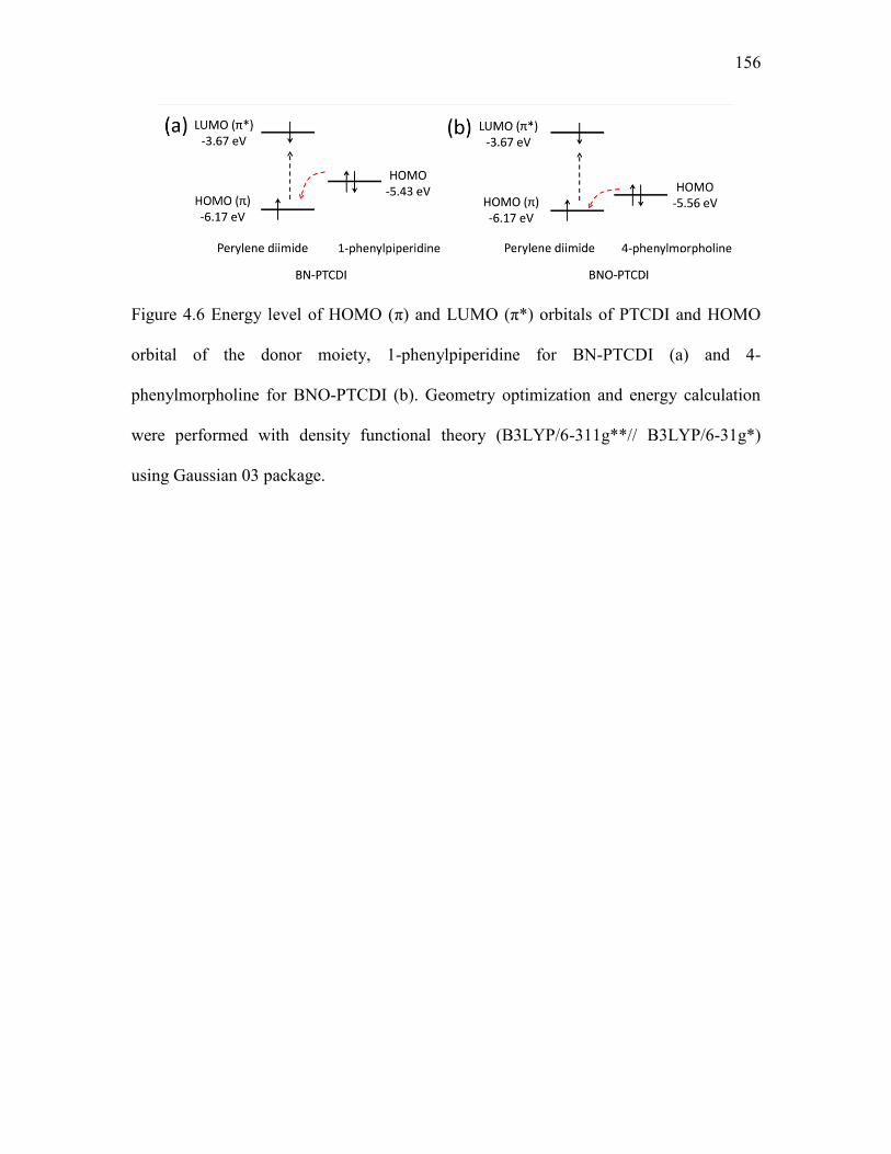
156
Figure 4.6 Energy level of HOMO (π) and LUMO (π*) orbitals of PTCDI and HOMO
orbital of the donor moiety, 1-phenylpiperidine for BN-PTCDI (a) and 4-
phenylmorpholine for BNO-PTCDI (b). Geometry optimization and energy calculation
were performed with density functional theory (B3LYP/6-311g**// B3LYP/6-31g*)
using Gaussian 03 package.

157
5 10 15 20 25 300.0
5.0x10³
1.0x10⁴
1.5x10⁴
2.0x10⁴
2.5x10⁴
5 10 15 20 25 300.0
5.0x10²
1.0x10³
1.5x10³
2.0x10³
2.5x10³
Inte
nsit
y
2Theta (degree)
BN-PTCDI
BNO-PTCDI
DD-PTCDI
(11.57 Å) (8.28 Å)(6.91 Å) (4.81 Å)
(11.61 Å) (8.40 Å)
(6.87 Å) (4.76 Å)
002 (12.50 Å)
003 (8.18 Å)
(7.19 Å)
(6.89 Å)
004 (6.09 Å)
006 (4.39 Å)
007 (3.80 Å)
Inte
ns
ity
2Theta (degree)
001 (25.38 Å)
(22.89 Å)
(23.49 Å)
Figure 4.7 X-ray diffraction patterns of BN-PTCDI, BNO-PTCDI and DD-PTCDI
nanofibers. The inset is the enlarged spectrum in the degree range from 6° to 30°.

158
Figure 4.8 Differential scanning calorimetry (DSC) traces of the BN-PTCDI, BNO-
PTCDI and DD-PTCDI nanofibers. The data shown are from the second heating-cooling
cycle.
0 50 100 150 200 250
Heat
flo
w
Temperature (C)
Heating
Cooling
HeatingCooling
Heating
Cooling
BN-PTCDI
BNO-PTCDI
DD-PTCDI

159
400 450 500 550 600 650 700
0.00
0.03
0.06
0.09
0.12
0.15
0.18
Wavelength (nm)
0
200
400
600
800
BN-PTCDI
400 450 500 550 600 650 700
0.00
0.03
0.06
0.09
0.12
0.15
0.18
Wavelength (nm)
0
200
400
600
800
BNO-PTCDI
400 450 500 550 600 650 700
0.00
0.03
0.06
0.09
0.12
0.15
0.18
Ab
so
rpti
on
Wavelength (nm)
Ab
so
rpti
on
(a)
(b)
(c)
0
200
400
600
800
Flu
ore
sc
en
ce
In
ten
sit
y F
luo
res
ce
nc
e In
ten
sit
y
Ab
so
rpti
on
Flu
ore
sc
en
ce
In
ten
sit
y
DD-PTCDI
Figure 4.9 UV-vis absorption (black solid) and fluorescence (black dash) spectra of (a)
BN-PTCDI, (b) BNO-PTCDI, and (c) DD-PTCDI dissolved in chloroform (2 μmol L1).
Under the same measurement conditions, the fluorescence intensities of BN-PTCDI and
BNO-PTCDI solution were much lower than that of DD-PTCDI, but the quenched
fluorescence could be recovered by addition of hydrochloric acid (0.1 mol L1), for which
both the UV-vis absorption (red solid) and fluorescence (red dash) spectra were then
measured again under the same conditions.

160
Figure 4.10 Morphologies, UV-vis absorption, fluorescence emission of PTCDI
nanofiber thin films: (a, d, g) bright-filed and (b, e, h) fluorescence optical microscopy
images of BN-PTCDI, BNO-PTCDI and DD-PTCDI nanofibers, respectively; (c, f, i)
UV-vis absorption (black) and fluorescence (red) spectra of BN-PTCDI, BNO-PTCDI
and DD-PTCDI nanofibers, respectively. The excitation wavelength for the fluorescence
spectrum was 510 nm.

161
Table 4.1 Activation energy (EA) estimated for the three PTCDI nanofibers in the low and
high temperature range from both the dark current and photocurrent measurements.
Sample
EA in dark (meV) EA under illumination (meV)
25 – 80 °C 80 – 120 °C 25 – 80 °C 80 – 120 °C
BN-PTCDI 628 1077 467 868
BNO-PTCDI 465 915 263 628
DD-PTCDI 169 549 127 566
CHAPTER 5
DISSERTATION CONCLUSIONS AND PROPOSED
FUTURE WORK
5.1 Dissertation Conclusions
This dissertation is primarily focused on the investigation of electrical properties and
potential applications of PTCDI nanofibers with D-A structure. We have designed new
PTCDI molecules by substituting one of the imide sides with amine groups (as strong
donor) and fabricated them into nanofibers via solution self-assembling. The materials
structures, and their optical and electrical properties, were systematically characterized
and studied. Moreover, the potential applications of these PTCDI nanofibers have also
been explored.
First, we demonstrated a unique chemical self-doping method that could increase the
electrical conductivity of a PTCDI-based molecule via a 1D stacking arrangement of D-A
PTCDI molecules. The D-A structure is based on 1-methylpiperidine-substituted PTCDI
(MP-PTCDI), of which the MP moiety is a strong electron donor, and can form a charge
transfer complex with the PTCDI moiety on the other molecule (acting as the acceptor) of
an adjacent stacked molecule, generating anionic radical of PTCDI (electron). Upon self-
assembling into nanoribbons, the electron generated is delocalized along the long axis of
PTCDIs through columnar π−π stacking, leading to enhancement in conductivity. The

163
resultant PTCDI radicals function as n-type dopants located in the lattice of PTCDI
crystals, in contrast to the interstitial doping reported for many other organic
semiconductors. With the high conductivity and n-type character, the MP-PTCDI
nanoribbons fabricated had highly sensitive responses to H2O2 vapor which is a critical
signature for improvised peroxide explosives. The lowest detected concentration was
down to 0.6 ppm and high selectivity toward H2O2 vapor against water and other
common organic liquids’ vapor. This work provides a simple and efficient approach to
fabricating self-doped organic semiconductors with high conductivity by molecular
engineering. In addition, the highly conductive PTCDI-based nanofibril materials can
potentially be fabricated into a small, light and low-power sensor device for public safety
screening and monitoring.
Second, we further studied the persistent photoconductivity (PPC) in PTCDI
nanofiber materials by using MP-PTCDI as a case study. It was found that the PTCDI
molecules containing strong electron donor groups demonstrated significant PPC when
fabricated into nanofiber materials. The donor-acceptor interaction, particularly under
photoexcitation, creates charge separation and electrostatic traps, thus producing potential
barriers that hinder the recombination of electron-hole pairs. The extended electron
delocalization along the π−π stacking (the long axis of nanofiber) further enhances the
charge separation, creating more charge relevant defects, resulting in a more pronounced
PPC. The temperature dependence of PPC decay time revealed the activation barrier
(energy) of 137 meV, which is close to that obtained in the inorganic semiconductors
such as n-type GaN. This systematic investigation of the PPC effect in PTCDI nanofibers
will provide deep insight into the charge carrier storage and relaxation process within

164
organic semiconductor materials, thus providing structural design rules for optimizing the
photovoltaic and photocatalytic performance of these materials.
Finally, we designed and synthesized more PTCDI molecules with D-A structure (1-
phenylpiperidine substituted PTCDI, BN-PTCDI, and 4-phenylmorpholine substituted
PTCDI, BNO-PTCDI). Thermoactivated electrical conductivity has been studied on these
two D-A PTCDIs and a control sample DD-PTCDI, which is a symmetric molecule with
both sides substituted with n-dodecyl chains. The results supported the thermoactivated
hopping mechanism for the charge transport, for which the activation energy was found
to be primarily dependent on the D-A structure. The D-A nanofibers showed significantly
higher activation energy than the DD-PTCDI nanofibers for both the dark current and
photocurrent measurements. D-A structure helps create disorder regarding both the
charge-transfer and diploe-dipole interactions between stacked molecules, and the
increased disorder enlarges the activation barrier. At higher temperatures, polaronic self-
trapping may become more dominant in controlling the charge hopping process. In
addition, the photocurrent measurement offers an alternative way to the gate control in
FET devices to modulate the charge density in material, which allows for investigating
the effect of charge density on the thermoactivation of charge hopping.
5.2 Suggestions for Future Work
This dissertation work has provided us deeper insight into the structure and electrical
properties of PTCDI nanofibers with D-A structure, as well as the structure-property
relationship of these materials. The following suggestions are recommended for
continuing research on the 1D nanostructures of D-A PTCDIs.

165
5.2.1 More Detailed Mechanism Study of PTCDI
Molecules With D-A Structure
The current study on PTCDI molecules with D-A structure has demonstrated some
interesting structure-property relationships. In the chemical self-doping PTCDI
nanofibers project, we have proven the formation of PTCDI anionic radicals, which acted
as the n-type dopants. However, a more detailed mechanism will be needed to assist
designing more suitable PTCDI molecules with high conductivity. One important factor
is the link distance between donor groups and the perylene diimide core because it affects
both the intramolecular and intermolecular D/A interactions, as well as the cofacial D/A
packing.1 For future work, we can systematically study the influence of linker distance by
changing the alkyl groups between the PTCDI core and donor groups. At the same time,
molecular self-assembly patterns can also be modified to study the influence of molecule
stacking patterns to the self-doping. The aim of the future study is to achieve structure-
controllable self-doping in PTCDI-based materials.
More nanofiber structure characterization, such as single crystal X-ray
crystallography or Grzaing incidence X-ray diffractometry (GIXD),2 will be valuable for
providing more detailed information on the nanofibers’ structure. Moreover, the transient
absorption spectroscopy can also be used to confirm and characterize the charge-
separated state directly.3
5.2.2 Applications of PTCDI Molecules With D-A Structure
The PPC effect has been observed in PTCDI nanofibers with D-A structures. These
types of materials can be used in photovoltaics and photocatalysis systems. In future

166
work, n-type D-A PTCDI nanofibers with PPC effect, such as MP-PTCDI, can be
integrated with p-type OSCs, such as P3HT to fabricated BHJ solar cells, to study their
performance,4 which is expected to provide significantly increased photoconversion
efficiency if the device is fabricated with well established processes and techniques. In
addition, such PTCDI-based materials can also be applied into photocatalysis systems for
photocatalytic splitting of water for H2,5,6 or for photocatalytic removal of pollutants.7
The PTCDI molecules with D-A structure demonstrated improved sensitivity toward
temperature. We can adapt such materials into wearable sensor systems for human-
activity monitoring and personal healthcare,8 where temperature fluctuation plays critical
roles. Additionally, the temperature sensor devices with D-A PTCDI molecules can be
fabricated into FETs to further enhance the sensitivity because increasing gate voltage
can increase the charge density.
5.3 References
(1) Wang, T.; Weerasinghe, K. C.; Sun, H.; Hu, X.; Lu, T.; Liu, D.; Hu, W.; Li, W.;
Zhou, X.; Wang, L. Effect of Triplet State on the Lifetime of Charge Separation in
Ambipolar D-A1-A2 Organic Semiconductors. J. Phys. Chem. C 2016, 120, 11338-
11349.
(2) Krauss, T. N.; Barrena, E.; Zhang, X. N.; de Oteyza, D. G.; Major, J.; Dehm, V.;
Würthner, F.; Cavalcanti, L. P.; Dosch, H. Three-Dimensional Molecular Packing of Thin
Organic Films of PTCDI-C8 Determined by Surface X-Ray Diffraction. Langmuir 2008,
24, 12742-12744.
(3) Walsh, J. J.; Lee, J. R.; Draper, E. R.; King, S. M.; Jäckel, F.; Zwijnenburg, M. A.;
Adams, D. J.; Cowan, A. J. Controlling Visible Light Driven Photoconductivity in Self-
Assembled Perylene Bisimide Structures. J. Phys. Chem. C 2016, 120, 18479-18486.
(4) Li, L.; Jacobs, D. L.; Bunes, B. R.; Huang, H.; Yang, X.; Zang, L. Anomalous High
Photovoltages Observed in Shish Kebab-Like Organic p-n Junction Nanostructures.
Polym. Chem. 2014, 5, 309-313.
(5) Chen, S.; Jacobs, D. L.; Xu, J.; Li, Y.; Wang, C.; Zang, L. 1D Nanofiber Composites

167
of Perylene Diimides for Visible-Light-Driven Hydrogen Evolution From Water. RSC
Adv. 2014, 4, 48486-48491.
(6) Chen, S.; Li, Y.; Wang, C. Visible-Light-Driven Photocatalytic H2 Evolution From
Aqueous Suspensions of Perylene Diimide Dye-Sensitized Pt/TiO2 Catalysts. RSC Adv.
2015, 5, 15880-15885.
(7) Dong, G.; Yang, L.; Wang, F.; Zang, L.; Wang, C. Removal of Nitric Oxide through
Visible Light Photocatalysis by g-C3N4 Modified With Perylene Imides. ACS Catal.
2016, 6, 6511-6519.
(8) Someya, T.; Kato, Y.; Sekitani, T.; Iba, S.; Noguchi, Y.; Murase, Y.; Kawaguchi, H.;
Sakurai, T. Conformable, Flexible, Large-Area Networks of Pressure and Thermal
Sensors With Organic Transistor Active Matrixes. Proc. Natl. Acad. Sci. U. S. A. 2005,
102, 12321-12325.