Embed Size (px)
Citation preview
Realization of two-dimensional crystal of ions in a monolithic Paul trap
Ye Wang1,2,∗ Mu Qiao1, Zhengyang Cai1, Kuan Zhang3,1, Naijun Jin1, Pengfei Wang1, Wentao
Chen1, Chunyang Luan1, Haiyan Wang1, Yipu Song1, Dahyun Yum1,4, and Kihwan Kim1†1 Center for Quantum Information, Institute for Interdisciplinary Information Sciences,
Tsinghua University, Beijing 100084, P. R. China2Fitzpatrick Institute for Photonics, Electrical and Computer Engineering Department,
Duke University, Durham, North Carolina 27708, USA3MOE Key Laboratory of Fundamental Physical Quantities Measurements,
Hubei Key Laboratory of Gravitation and Quantum Physics, PGMF and School of Physics,Huazhong University of Science and Technology, Wuhan 430074, China
4Department of physics and astronomy Seoul National University, South Korea 08826(Dated: December 11, 2019)
We present a simple Paul trap that stably accommodates up to a couple of dozens 171Yb+ ionsin a stationary two-dimensional lattice. The trap is constructed on a single plate of gold-platedlaser-machined alumina and can produce a pancake-like pseudo-potential that makes ions form aself-assembly two-dimensional crystal which locates on the plane composed of axial and one of thetransverse axes with around 5 µm spacing. We use Raman laser beams to coherently manipulatethese ion-qubits where the net propagation direction is perpendicular to the plane of the crystal andmicromotion. We perform the coherent operations and study the spectrum of vibrational modesthrough globally addressed Raman laser-beams on a dozen of ions in the two-dimensional crystal.We measure the amplitude of micro-motion by comparing the strengths of carrier and micro-motionsideband transitions with three ions, where the micro-motion amplitude is similar to that of a singleion. The spacings of ions are small enough for large coupling strengths, which is a favorable conditionfor two-dimensional quantum simulation.
Two-dimensional crystal of ions can be an attractiveand natural platform to scale up the number of ion-qubitsin a single trap and to explore many-body quantum mod-els in two-dimension [1–16]. Recently, a fully-connectedquantum computer has been realized with up to 5-20ions forming one-dimensional (1D) crystal in linear Paultraps [17, 18] and over 50 ion-qubits have been used fora quantum simulation with restricted control[19]. Extra-dimension of the crystal can provide a quadratic scal-ing of the number of ion-qubits in the trap. Ion-qubitsin the two-dimensional (2D) crystal intrinsically has 2Dlaser-induced interactions, which facilitates to study 2Dmany-body physics through quantum simulation such asgeometric frustration, topological phase of matter, etc.[9–13].
There have been deliberate proposals and experimentalexertions to confine ions in a 2D lattice[1–8, 15, 20–22].In the Penning trap that uses static magnetic field anddc voltages for the confinement, hundreds of ions forma rotating 2D crystal [23]. Effective Ising interactionsamong ion-qubits in the 2D crystal have been engineered[1], and entanglement of spin-squeezing has been studied[2]. Due to a high magnetic field condition and the fastrotation of ions in Penning traps, however, no clock-stateof an ion can represent an effective spin, and it is chal-lenging to implement individual spin controls with laserbeams.
Paul traps do not require high magnetic fields for con-finement of ions and can be an alternative platform toimplement 2D crystal. The main difficulty in Paul trapfor producing 2D crystal of ions for quantum computa-
tion or quantum simulation lies in the existence of mi-cromotion [24] synchronous with the oscillating electricfield that introduces phase modulations on laser beamsfor cooling and coherent operation. The micromotioncan be nullified at a point or in a line, but not in aplane. To address the micromotion problem, arrays ofmicro traps have been proposed [3, 4] and small scale ofarrays traps have been implemented [7, 8]. Due to rela-tively large distances between micro traps, however, theCoulomb-coupling strength between ion-qubits in differ-ent traps would be relatively weak and so as the effectivespin-spin interactions induced by laser beams of coherentoperations [25–27]. Alternatively, it has been proposedto produce a trap, where the direction of micromotionis perpendicular to the net-propagation direction of laserbeams for coherent control [12, 13]. Such a trap struc-ture is relatively simple to manufacture and can easilyhold tens to hundreds of ions.
Here, we report the implementation of a Paul trap thataccommodates tens of ions in a 2D crystal. The trap isa three-dimensional monolithic trap [28–30] constructedon a single layer of gold-plated laser-machined alumina[31, 32]. We carefully design the structure of the trapelectrodes to precisely control the orientation of principleaxis and ensure perpendicularity between the micromo-tion axis and the net-propagation direction of coherentoperation Raman laser beams. The 2D crystal is locatedon the plane composed of axial and one of transverseaxes, which is simply imaged to an electron-multiplyingCCD (EMCCD) camera. We perform coherent opera-tions on ion-qubits and study the spectrum of vibrational
arX
iv:1
912.
0426
2v2
[qu
ant-
ph]
10
Dec
201
9
2
modes through globally addressed Raman laser beams.We measure the amplitude of micro-motion by compar-ing the strengths of carrier and micro-motion sidebandtransitions with three ions, where the modulation indexsimilar to that of single ion. The strengths of effectivespin-spin couplings can be similar to the values in cur-rent linear traps, which is a favorable condition for 2Dquantum simulation.
oven
shielding
(c)
(b)(a)
RFRaman
Cooling
CoolingOptical PumpingDetecting
Repumping
Bz
x y
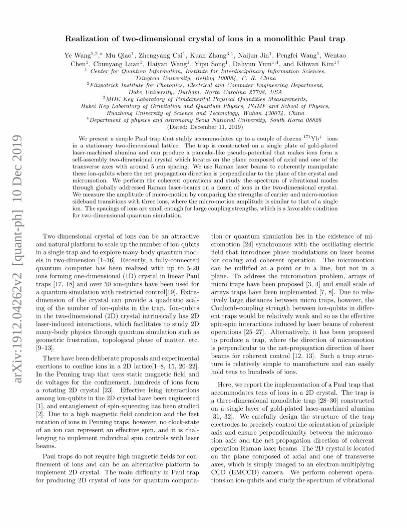
FIG. 1. Trap structure and beam configuration. (a)Conceptual drawing of our trap and the configuration of laserbeams for cooling, pumping, detection (370 nm and 935 nm)and coherent operations (355 nm). The magnetic field is ap-plied vertically. (b) Scanning electron microscope (SEM) im-age of our trap (white scale bar, 400 µm). The trap structureis laser-machined on a single piece of alumina with less than10 µm precision. Gold is electro-plated on the surface of alu-mina with 10 µm thickness. The trap has a total of 20 elec-trodes, where fourteen of them are connected to GND and theothers to DC sources. The gray letters label the electrodeson the opposite side of the trap.(c) Image of our monolithictrap mounted in a hemi-sphere vacuum chamber. The trapis shielded with stainless steel plates on the front and back,respectively, which are connected to GND. The dashed linesshow the electrodes underneath of the shield.
Our trap is fabricated in a single piece of alumina platewith gold-coating, with more details in Appendix B. Fig.1 shows the structure of our trap. The trap is monolithicand functionally separated into three layers, where frontand back layers contain dc electrodes, and the middlelayer is used for RF electrode as conceptually shown inFig. 1(a). The RF electrode has a slope with the an-gle of 45 relative to the normal direction of the aluminapiece. In each DC layer, there are ten electrodes, fiveelectrodes on both upside and downside with a 50 µmspacing. At the center of the trap, there is a 260 µm ×4 mm slot, where ions are trapped. The Fig. 1(b) showsfront side of the trap. The angle of the slope and the gapbetween DC and RF electrodes are optimized to maxi-mize the trap frequency (see Appendix A for the designconsideration). We use CPO (Charged Particle Optics)software to calculate the electric potential from the elec-trodes. We also compare the simulated potential withthe real potential to calibrate the simulation coefficient
for further trap simulation (see Appendix D). In the ex-periment, only six of twenty electrodes are connected tothe stable DC sources, and the others to GND, as shownin Fig. 1(b).
The monolithic trap is located in a vacuum chambershown in Fig 1(c). The trap and vacuum system is de-signed to ensure sufficient optical accesses. 171Yb+ ionsare loaded to the middle of the trap by photo-ionizationand Doppler cooling [33]. We create the 2D crystal of ionsin a plane that consists of the axial axis (x-axis) and oneof the radial axes (z-axis). We apply two Doppler-coolinglaser beams to couple all the three directions of ion mo-tions, as shown in Fig. 1(a). The magnetic-field insen-sitive states of 171Yb+ ion in the ground-state manifold2S1/2, |F = 0,mF = 0〉 and |F = 1,mF = 0〉 are mappedto qubit state |0〉 and |1〉, respectively. The state ofthe qubit is detected by the laser beam resonant to thetransition between F = 1 of 2S1/2 and F = 0 of 2P1/2
and initialized to |0〉 by applying the optical pumpinglaser beam resonant with the transition between F = 1of 2S1/2 and F = 1 of 2P1/2. The qubit is coherentlymanipulated by a pair of 355 nm picosecond pulse laserbeams with beatnote frequency about the qubit transi-tion ω0 = 2π × 12.642821 GHz.
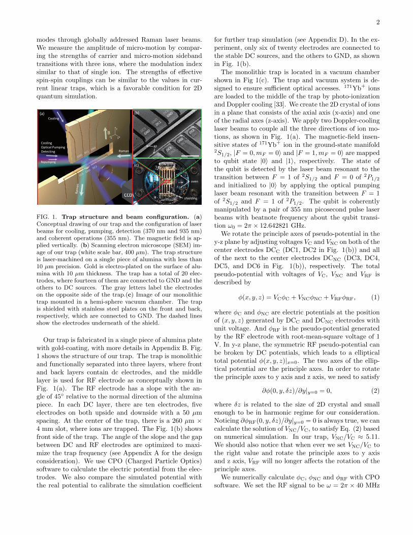
We rotate the principle axes of pseudo-potential in they-z plane by adjusting voltages VC and VNC on both of thecenter electrodes DCC (DC1, DC2 in Fig. 1(b)) and allof the next to the center electrodes DCNC (DC3, DC4,DC5, and DC6 in Fig. 1(b)), respectively. The totalpseudo-potential with voltages of VC, VNC and VRF isdescribed by
φ(x, y, z) = VCφC + VNCφNC + VRFφRF, (1)
where φC and φNC are electric potentials at the positionof (x, y, z) generated by DCC and DCNC electrodes withunit voltage. And φRF is the pseudo-potential generatedby the RF electrode with root-mean-square voltage of 1V. In y-z plane, the symmetric RF pseudo-potential canbe broken by DC potentials, which leads to a ellipticaltotal potential φ(x, y, z)|x=0. The two axes of the ellip-tical potential are the principle axes. In order to rotatethe principle axes to y axis and z axis, we need to satisfy
∂φ(0, y, δz)/∂y|y=0 = 0, (2)
where δz is related to the size of 2D crystal and smallenough to be in harmonic regime for our consideration.Noticing ∂φRF(0, y, δz)/∂y|y=0 = 0 is always true, we cancalculate the solution of VNC/VC, to satisfy Eq. (2) basedon numerical simulation. In our trap, VNC/VC ≈ 5.11.We should also notice that when ever we set VNC/VC tothe right value and rotate the principle axes to y axisand z axis, VRF will no longer affects the rotation of theprinciple axes.
We numerically calculate φC, φNC and φRF with CPOsoftware. We set the RF signal to be ω = 2π × 40 MHz
3
and VRF = 80 V. When VNC/VC =∞ with VNC = 1.5 V,vertical principle axis (green line in Fig. 2(a)) is clock-wise rotated by 22.9 from the z-axis. When the ratioVNC/VC = 0 with VC = 1.5 V, the green axis is counter-clockwise rotated by 5.7 from the z-axis. As shown inFig. 2(b), when the ratio VNC/VC = 5.11, the green axisis in line with z-axis.
0.2
0.1
0.0
-0.1
-0.2-0.2 -0.1 0.0 0.1 0.2mm
mm0.2
0.1
0.0
-0.1
-0.2-0.2 -0.1 0.0 0.1 0.2mm
mm(a) (b)
Raman Δ𝑘 Raman Δ𝑘𝜔z
𝜔y
𝜔z
𝜔y
(c) (d)−𝜔z
−𝜔y
𝜔z
𝜔y
−𝜔y𝜔y
0.5
0.02-2
0.5
0.02-2
P() P()
-1 0 1(𝜔0 − 𝜔R)/(2𝜋) (MHz)
-1 0 1(𝜔0 − 𝜔R)/(2𝜋) (MHz)
𝜔z
𝜔y
𝜔x
(e)
Trap
fre
qu
ency
(M
Hz)
0.0
0.5
1.0
1.5
2.0
140 155 170 185 200 215
RF Voltage (V)
10 ions20 ions
100 ions200 ions
y
z
y
z
FIG. 2. Principle axis rotation (a) The contour plot ofpseudo-potential when VNC/VC = ∞, central electrodes areconnected to GND. (b) The contour plot of pseudo-potentialwhen the principle axes are overlapped with y and z axes,where the voltage ratio is VNC/VC = 5.11. (c) The Ramanspectrum with principle axes in the condition of (a), wherewe can see both of the transverse modes. (d) The Ramanspectrum with principle axes in the condition of (b). In thissituation, the Raman beams can only drive the mode of they-axis, not that of the z-axis. (e) Relation between two radial-mode frequencies and the RF voltages. By merely changingthe RF voltage, we can realize different ratios of trap frequen-cies. The red dots are the experimental data, the dark linesare the fitting results. The dashed lines, which are calculatedby ωy/(2.264N)1/4 for different RF voltage, are the up boundsof the region where the symmetric 2D crystal can be formedfor different numbers of ions.
We experimentally confirm the rotation of the princi-
ple axes in y-z plane with single ion by observing thedisappearance of the Raman coupling to z-axis vibra-tional mode. The spectrum of vibrational modes, asshown in Fig. 2(c)(d) is measured by the following pro-cedure: 1) we perform Doppler cooling on ion-crystal,which results in thermal states with n ≈ 7.1, Dopplercooling limit, and initialize the internal states to |↓〉 byapplying the standard optical pumping technique. 2) Weapply Raman beams with a net k-vector perpendicularto the z-axis. Once the beatnote-frequency ωR of Ra-man beams matching to ω0 ± ωy,z, sideband transitionsoccurs [34], which can be detected by the fluorescenceof ions that is collected by imaging system and PMT(Photo-multiplier tube). In Fig. 2(c), the voltage ratiois close to the condition of VNC/VC = ∞ in Fig. 2(a),where the principle axes are tilted away from y-z axes.The net k-vector of Raman beams is along the y-axis,which can excite both directions of vibrational modes.Thus, two peaks in blue-sidebands (δ = ωy,z) as well asred-sidebands (δ = −ωy,z) are clearly visible in Fig. 2(c),where detuning δ = ωR − ω0. However, when the prin-ciple axes are rotated to y-z axes as shown in Fig. 2(b),Raman beams cannot excite the vibrational mode alongz-axis, which results in vanishing a peak in the Ramanspectrum. Based on the spectrum of Fig. 2(d), we esti-mate that deviation of the principle axes from y-z axesis below 0.40.
In order to produce a 2D ion crystal in z-x plane, weneed to satisfy ωy > (2.264N)1/4ωx,z [13, 35]. First, keep-ing the principle axes to y-z axes, we can calculate thevoltage solution for DC electrodes with a given axial trapfrequency ωx. With determined DC potential, the rela-tion between ωy and ωz is given by [34]
ω2y − ω2
z = CVNC, (3)
(see Appendix C) where C is a positive constant deter-mined by the trap geometry. In the case of VRF = 0,the z-axis potential, the shallower potential respective tothat of the y-axis according to Eq. (3), becomes anti-harmonic, which indicates ω2
z < 0 and ω2y < CVNC. On
the other hand, since ωyand ωz are monotonously in-crease with VRF, there is a critical value of VRF thatmakes ω2
y = CVNC and ω2z = 0. Therefore, we can tune
ωy from√CVNC to∞, ωz from near zero to∞ by tuning
VRF. As shown in Fig. 2(e), with different values of VRF,we can have ωz/ωx from 0 to 2.72 for 10 ions to realize2D ion crystal with different aspect ratios.
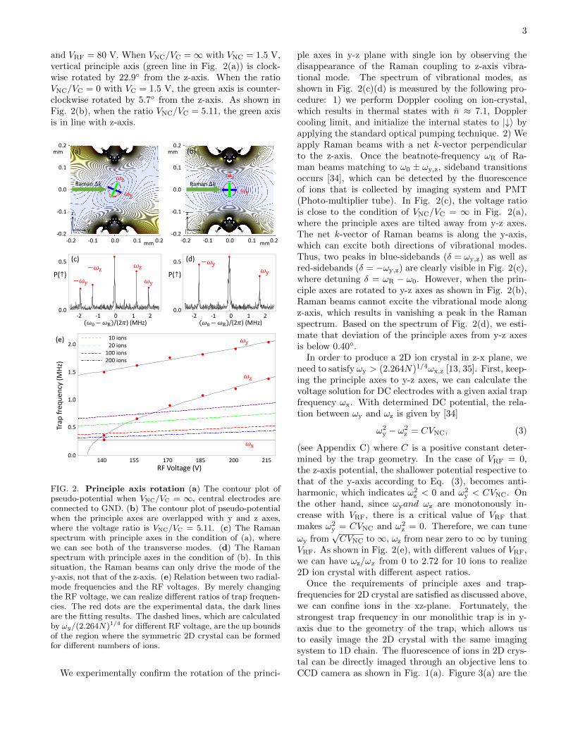
Once the requirements of principle axes and trap-frequencies for 2D crystal are satisfied as discussed above,we can confine ions in the xz-plane. Fortunately, thestrongest trap frequency in our monolithic trap is in y-axis due to the geometry of the trap, which allows usto easily image the 2D crystal with the same imagingsystem to 1D chain. The fluorescence of ions in 2D crys-tal can be directly imaged through an objective lens toCCD camera as shown in Fig. 1(a). Figure 3(a) are the
4
(b)
𝛿(𝜔0 − 𝜔R)/(2𝜋) (MHz)
(a)
x
z
0.5
0.0
1.0
Experiment
TheoryPavg()
1.1 1.2 1.3 1.4 1.5
FIG. 3. Geometry and mode structure of 2D-ion crys-tals. (a) CCD images of 10,19, and 25 ion crystals withdifferent trap frequencies. The above ones are raw data takenfrom EMCCD, and the bottom ones compare the numericalsimulation and the real data where the white cycles are thepositions of ions read out from the CCD pictures and the redpoints are simulation results. The white scale bars represent 5µm distance. (b) Raman spectrum of the 2D crystal with tenions. The black curve is the experiment result and the redlines are the theoretical prediction of the mode frequencies[13].
images of the 2D crystals and demonstrate the controlcapability for shapes of 2D crystals with various settingsof trap frequencies. For the image of 10 ions, the trap fre-quencies are ωx, ωy, ωz/(2π) = 0.427, 1.5, 0.561MHz.For the image of 19 ions and 25 ions the trap frequen-cies are ωx, ωy, ωz/(2π) = 0.28, 1.50, 0.26MHz andωx, ωy, ωz/(2π) = 0.28, 1.63, 0.68MHz respectively.For 25 ions, these frequencies look violating the bound forthe 2D crystal in Fig. 2(e). However, it is a complicatedsituation since one of the frequencies, ωx, is still belowthe bound. We numerically study the situation carefullyand discuss in the Appendix E. The geometries of thecrystal are in agreement with the numerical simulation.We simulate the geometry configuration of the ion crys-tal by numerically minimizing the electrical potential ofthe ions in a three dimensional harmonic trap [13].
We first verified the dimension of the crystal by imag-ing the crystal, but it is hard to distinguish whether thereare any ions out of the ion crystal plane by an objectivelens with finite depth of field. The dimension of the crys-tal is further verified by measuring the transverse mode
structure. Similar to the single ion case, we drive the dif-ferent transverse modes of a 10-ion crystal by varying thedetuning between Raman beams. Fig 3(b) shows the re-sulting spectrum, where each peak represent a motionalmode in the y-axis. The mode spectrum is consistentwith the theoretical simulation based on trap frequen-cies and geometry of 2D ion crystal[13]. Similar to lin-ear chain case[36], when the phase transition from a 2Dcrystal to a 3D crystal happens the minimal frequencyof the mode along the y-axis will tend to be negative.Our measured mode frequencies are far away from zero,which confirm the dimension of the crystal is two.
Raman Δ𝑘
(a)1.0
0.5
0.00 20 40 60 80 100
1.0
0.5
0.00 250 500 750 1000
T(𝜇𝑠)
(b) Carrier
(c) Micro-motion sideband
Pavg()
Pavg()
y
z
T(𝜇𝑠)
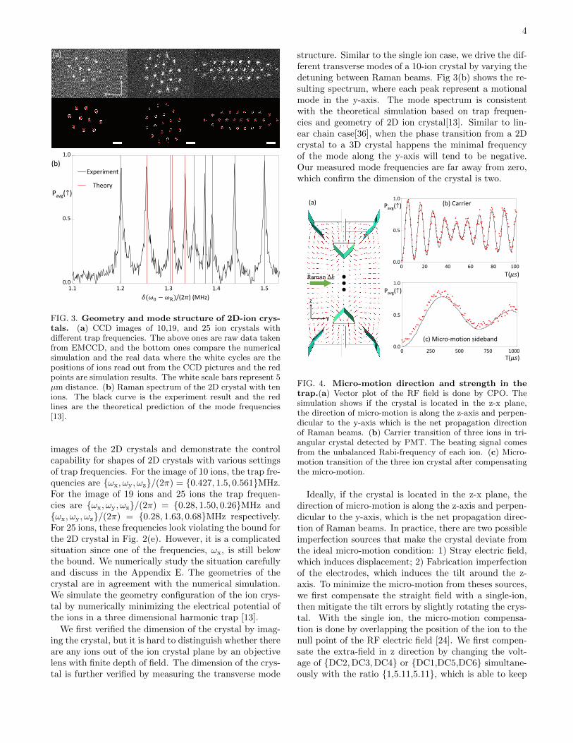
FIG. 4. Micro-motion direction and strength in thetrap.(a) Vector plot of the RF field is done by CPO. Thesimulation shows if the crystal is located in the z-x plane,the direction of micro-motion is along the z-axis and perpen-dicular to the y-axis which is the net propagation directionof Raman beams. (b) Carrier transition of three ions in tri-angular crystal detected by PMT. The beating signal comesfrom the unbalanced Rabi-frequency of each ion. (c) Micro-motion transition of the three ion crystal after compensatingthe micro-motion.
Ideally, if the crystal is located in the z-x plane, thedirection of micro-motion is along the z-axis and perpen-dicular to the y-axis, which is the net propagation direc-tion of Raman beams. In practice, there are two possibleimperfection sources that make the crystal deviate fromthe ideal micro-motion condition: 1) Stray electric field,which induces displacement; 2) Fabrication imperfectionof the electrodes, which induces the tilt around the z-axis. To minimize the micro-motion from theses sources,we first compensate the straight field with a single-ion,then mitigate the tilt errors by slightly rotating the crys-tal. With the single ion, the micro-motion compensa-tion is done by overlapping the position of the ion to thenull point of the RF electric field [24]. We first compen-sate the extra-field in z direction by changing the volt-age of DC2,DC3,DC4 or DC1,DC5,DC6 simultane-ously with the ratio 1,5.11,5.11, which is able to keep

5
the principle axes direction and avoid generating the dis-placement along y axis. We can also change the voltageof electrodes DC1,DC3,DC4 or DC2,DC5,DC6 withratio 1,5.11,5.11 to compensate the extra-field in y di-rection. For the z-axis compensation, we minimize thechange of ion position depending on RF power and forthe y-axis compensation, we minimize the micro-motionsideband transition of Raman beams. For the error in-duced by the fabrication imperfection, we slightly changethe voltage of electrodes DC3,DC4,DC5,DC6 with ra-tio 1,1,1,1 to rotate the crystal around x axis and withratio 1,-1,1,-1 to rotate the crystal around z axis. Withthe control, we also minimize the Rabi-frequency of themicro-motion sideband transition with three ions.
The strength of the micro-motion is quantified by mea-suring the ratio between two Rabi frequencies of the car-rier and the micro-motion transition[24]. We measure themicro-motion strength in a three-ion 2D crystal. We firstsequentially apply Doopler cooling and EIT cooling [37]to cool the 2D crystal down to near the motional groundstate. Then we drive the Rabi flopping and measure theRabi frequency of the carrier and the micro-motion side-band transition. For each flopping, we collect the overallcounts of three ions with PMT and fit the result withthree Rabi frequency. The fitting gives us three carrierπ-time 5.96, 5.40, 5.19µs and three micro-motion side-band π-time 474, 440, 317µs. The modulation index,which is given by β/2 = Ωmicro/Ωcarrier, has a maximunpossible value of 0.038 and a minimal possible value of0.021, which are similar to single ion situation.
We also experimentally study the heating of the vi-brational modes in our trap with a single ion. We firstprepare the ground-state of radial vibrational modes byRaman-sideband cooling, wait for a certain duration andmeasure average phonon-number n for the mode of in-terest. We estimate n by Fourier transforming the blue-sideband transitions [34]. We find that the heating rateof y-axis mode with the principle axes of 2D crystal (Fig.2(b)) is around 360 quanta per second, which is about 2.5times larger than that with the condition of Fig. 2(a). Itis understandable, since the noise of environmental elec-tric field along y-axis would be more severe than those ofthe other axes.
Our trap can be considered as an ideal platform forimplementing various proposals of quantum simulationswith 2D crystal [9–13]. It can be used to observe a struc-tural quantum phase transition from 2D to 3D with re-laxed requirements[38]. Incorporating the capability ofindividual control and detection, universal quantum com-putation also can be achieved with more number of qubitsthan in a linear chain. The capability of laser addressingin a two dimensional space has been demonstrated withdifferent techniques[39, 40]. The detection of individualions already has been well established using camera withhigh detection efficiency [41].
Furthermore, the 2D crystal is a natural platform for
the fault-tolerant quantum computation schemes with2D geometry, including the surface code[42], the Bacon-Shor code[43] and the (2+1) dimensional fault-tolerantmeasurement-based quantum computing[44–46]. The fullconnectivity of trapped-ion system provides the capabil-ity of implementing any fault-tolerant scheme withoutextra overhead at the circuit level[47]. However, to im-plement a 2D topological code on an 1D ion chain, onehas to map some local interactions to long distance gatesor shuttle the ions, which requires longer gate time[48–50]. With a 2D ion crystal, the locality of 2D topologicalcodes can be preserved, without the loss of full connec-tivity.
ACKNOWLEDGMENTS
We thank Jincai Wu and Haifeng Zhu at InterstellarQuantum Technology (Nanjing) Ltd for many useful dis-cussions on fabrication technique. This work was sup-ported by the National Key Research and DevelopmentProgram of China under Grants No. 2016YFA0301900and No. 2016YFA0301901 and the National Natural Sci-ence Foundation of China Grants No. 11374178, No.11574002, and No. 11974200.
Y.W. and M.Q contributed equally to this work.
APPENDIX
APPENDIX A: STRUCTURE OF THE TRAP
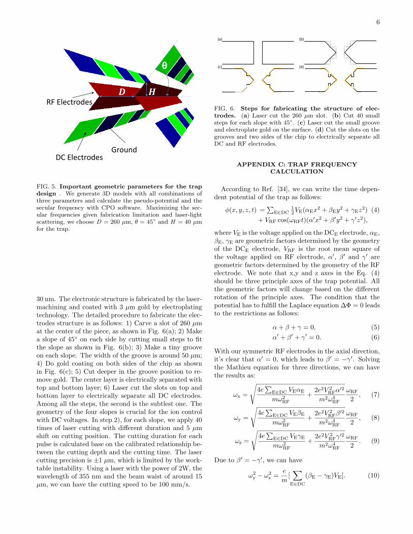
We use CPO software to simulate the trap performancewith various geometric parameters. There are three im-portant parameters for the trap design: the distance be-tween two RF electrodes D, the height of RF electrodesH, and the angle of the slope θ as shown in Fig 5. Weoptimize these three parameters mainly to achieve largesecular frequencies in the radial direction given fabrica-tion limitation. The secular frequency is approximatelyinverse-proportional to D2[34], which is inspected in ournumerical simulation. We balance the requirement oflarge trap frequency and low UV-light scattering, whichleads to the choice of D = 260 µm. For the slope angleθ, our simulation shows the best performance at θ ≈ 47.Due to the fabrication difficulty of the angle, we chooseθ = 45. Our simulation shows the best value of H isaround 30 µm. Considering the laser cutting precision,we decide H = 40 µm.
APPENDIX B: FABRICATION PROCESS
The substrate is a single piece of alumina with thethickness of 380 µm and the surface flatness of less than
6
𝑫 𝑯
DC ElectrodesGround
RF Electrodes
FIG. 5. Important geometric parameters for the trapdesign . We generate 3D models with all combinations ofthree parameters and calculate the pseudo-potential and thesecular frequency with CPO software. Maximizing the sec-ular frequencies given fabrication limitation and laser-lightscattering, we choose D = 260 µm, θ = 45 and H = 40 µmfor the trap.
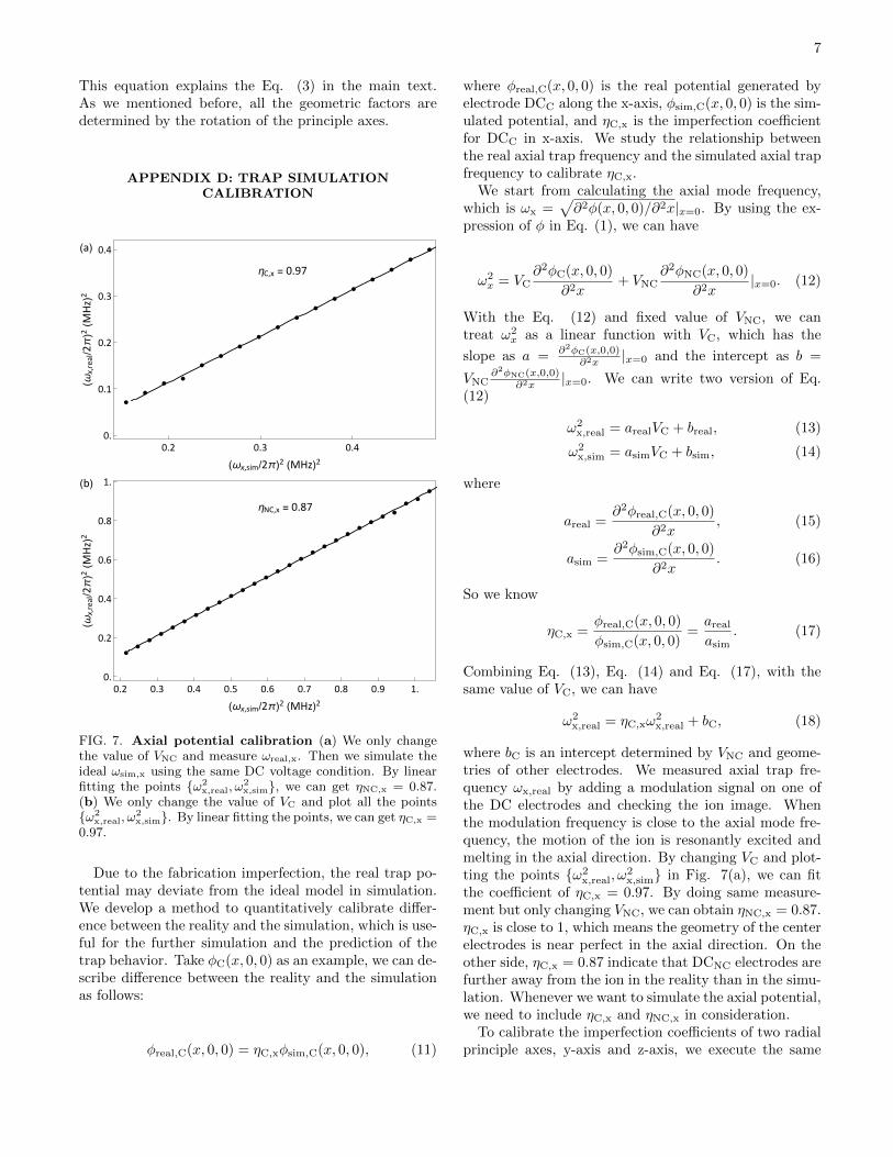
30 nm. The electronic structure is fabricated by the laser-machining and coated with 3 µm gold by electroplatingtechnology. The detailed procedure to fabricate the elec-trodes structure is as follows: 1) Carve a slot of 260 µmat the center of the piece, as shown in Fig. 6(a); 2) Makea slope of 45 on each side by cutting small steps to fitthe slope as shown in Fig. 6(b); 3) Make a tiny grooveon each slope. The width of the groove is around 50 µm;4) Do gold coating on both sides of the chip as shownin Fig. 6(c); 5) Cut deeper in the groove position to re-move gold. The center layer is electrically separated withtop and bottom layer; 6) Laser cut the slots on top andbottom layer to electrically separate all DC electrodes.Among all the steps, the second is the subtlest one. Thegeometry of the four slopes is crucial for the ion controlwith DC voltages. In step 2), for each slope, we apply 40times of laser cutting with different duration and 5 µmshift on cutting position. The cutting duration for eachpulse is calculated base on the calibrated relationship be-tween the cutting depth and the cutting time. The lasercutting precision is ±1 µm, which is limited by the work-table instability. Using a laser with the power of 2W, thewavelength of 355 nm and the beam waist of around 15µm, we can have the cutting speed to be 100 mm/s.
(a) (b)
(c) (d)
FIG. 6. Steps for fabricating the structure of elec-trodes. (a) Laser cut the 260 µm slot. (b) Cut 40 smallsteps for each slope with 45. (c) Laser cut the small grooveand electroplate gold on the surface. (d) Cut the slots on thegrooves and two sides of the chip to electrically separate allDC and RF electrodes.
APPENDIX C: TRAP FREQUENCYCALCULATION
According to Ref. [34], we can write the time depen-dent potential of the trap as follows:
φ(x, y, z, t) =∑
E∈DC12VE(αEx
2 + βEy2 + γEz
2) (4)
+ VRF cos(ωRFt)(α′x2 + β′y2 + γ′z2),
where VE is the voltage applied on the DCE electrode, αE,βE, γE are geometric factors determined by the geometryof the DCE electrode, VRF is the root mean square ofthe voltage applied on RF electrode, α′, β′ and γ′ aregeometric factors determined by the geometry of the RFelectrode. We note that x,y and z axes in the Eq. (4)should be three principle axes of the trap potential. Allthe geometric factors will change based on the differentrotation of the principle axes. The condition that thepotential has to fulfill the Laplace equation ∆Φ = 0 leadsto the restrictions as follows:
α+ β + γ = 0, (5)
α′ + β′ + γ′ = 0. (6)
With our symmetric RF electrodes in the axial direction,it’s clear that α′ = 0, which leads to β′ = −γ′. Solvingthe Mathieu equation for three directions, we can havethe results as:
ωx =
√4e
∑E∈DC VEαE
mω2RF
+2e2V 2
RFα′2
m2ω4RF
ωRF
2, (7)
ωy =
√4e
∑E∈DC VEβE
mω2RF
+2e2V 2
RFβ′2
m2ω4RF
ωRF
2, (8)
ωz =
√4e
∑E∈DC VEγE
mω2RF
+2e2V 2
RFγ′2
m2ω4RF
ωRF
2. (9)
Due to β′ = −γ′, we can have
ω2y − ω2
z =e
m[∑
E∈DC
(βE − γE)VE]. (10)
7
This equation explains the Eq. (3) in the main text.As we mentioned before, all the geometric factors aredetermined by the rotation of the principle axes.
APPENDIX D: TRAP SIMULATIONCALIBRATION
0.2 0.3 0.40.
0.1
0.2
0.3
0.4
(ωx,sim/2π)2 (MHz)2
(ωx,real/2
π)2
(MHz)2
(a)
ηC,x = 0.97
0.2 0.3 0.4 0.5 0.6 0.7 0.8 0.9 1.0.
0.2
0.4
0.6
0.8
1.
(ωx,sim/2π)2 (MHz)2
(ωx,real/2
π)2
(MHz)2
(b)
ηNC,x = 0.87
FIG. 7. Axial potential calibration (a) We only changethe value of VNC and measure ωreal,x. Then we simulate theideal ωsim,x using the same DC voltage condition. By linearfitting the points ω2
x,real, ω2x,sim, we can get ηNC,x = 0.87.
(b) We only change the value of VC and plot all the pointsω2
x,real, ω2x,sim. By linear fitting the points, we can get ηC,x =
0.97.
Due to the fabrication imperfection, the real trap po-tential may deviate from the ideal model in simulation.We develop a method to quantitatively calibrate differ-ence between the reality and the simulation, which is use-ful for the further simulation and the prediction of thetrap behavior. Take φC(x, 0, 0) as an example, we can de-scribe difference between the reality and the simulationas follows:
φreal,C(x, 0, 0) = ηC,xφsim,C(x, 0, 0), (11)
where φreal,C(x, 0, 0) is the real potential generated byelectrode DCC along the x-axis, φsim,C(x, 0, 0) is the sim-ulated potential, and ηC,x is the imperfection coefficientfor DCC in x-axis. We study the relationship betweenthe real axial trap frequency and the simulated axial trapfrequency to calibrate ηC,x.
We start from calculating the axial mode frequency,which is ωx =
√∂2φ(x, 0, 0)/∂2x|x=0. By using the ex-
pression of φ in Eq. (1), we can have
ω2x = VC
∂2φC(x, 0, 0)
∂2x+ VNC
∂2φNC(x, 0, 0)
∂2x|x=0. (12)
With the Eq. (12) and fixed value of VNC, we cantreat ω2
x as a linear function with VC, which has the
slope as a = ∂2φC(x,0,0)∂2x |x=0 and the intercept as b =
VNC∂2φNC(x,0,0)
∂2x |x=0. We can write two version of Eq.(12)
ω2x,real = arealVC + breal, (13)
ω2x,sim = asimVC + bsim, (14)
where
areal =∂2φreal,C(x, 0, 0)
∂2x, (15)
asim =∂2φsim,C(x, 0, 0)
∂2x. (16)
So we know
ηC,x =φreal,C(x, 0, 0)
φsim,C(x, 0, 0)=arealasim
. (17)
Combining Eq. (13), Eq. (14) and Eq. (17), with thesame value of VC, we can have
ω2x,real = ηC,xω
2x,real + bC, (18)
where bC is an intercept determined by VNC and geome-tries of other electrodes. We measured axial trap fre-quency ωx,real by adding a modulation signal on one ofthe DC electrodes and checking the ion image. Whenthe modulation frequency is close to the axial mode fre-quency, the motion of the ion is resonantly excited andmelting in the axial direction. By changing VC and plot-ting the points ω2
x,real, ω2x,sim in Fig. 7(a), we can fit
the coefficient of ηC,x = 0.97. By doing same measure-ment but only changing VNC, we can obtain ηNC,x = 0.87.ηC,x is close to 1, which means the geometry of the centerelectrodes is near perfect in the axial direction. On theother side, ηC,x = 0.87 indicate that DCNC electrodes arefurther away from the ion in the reality than in the simu-lation. Whenever we want to simulate the axial potential,we need to include ηC,x and ηNC,x in consideration.
To calibrate the imperfection coefficients of two radialprinciple axes, y-axis and z-axis, we execute the same

8
procedure as the axial calibration with more careful con-sideration about the principle-axes rotation. During theprocess of changing VNC or VC, only if we keep the ro-tation angle of the principle axes in a small regime, wecan have the similar equations as Eq. (18) for y-axis and
z-axis:
ω2y,real ≈ ηC,yω2
y,real + bC,y, (19)
ω2z,real ≈ ηC,zω2
z,real + bC,z, (20)
ω2y,real ≈ ηNC,yω
2y,real + bNC,y, (21)
ω2z,real ≈ ηNC,zω
2z,real + bNC,z. (22)
All the data is shown in Fig. 8. From the data and thelinear fitting, we can obtain ηC,y = 1.65, ηC,z = 1.92,ηNC,y = 1.23 and ηNC,z = 1.11. All these imperfec-tion coefficients are larger than 1, which indicates thatall, relative to the ideal model, the DC electrodes arecloser to the ion in the radial direction in the reality.When we simulate the radial potential and check theprinciple axes rotation in yz-plane, we use the averagevalue ηC,yz = 1/2(ηC,y + ηC,z) = 1.785 and ηNC,yz =1/2(ηNC,y + ηNC,z) = 1.17 to be the coefficients multi-plied to φC(0, y, z) and φNC(0, y, z).
8.8 9.1 9.4 9.7
9.
9.5
10.
10.5
(ωy,sim/2π)2 (MHz)2
(ωy,real/2
π)2
(MHz)2
(a)
ηC,y = 1.65
4.4 4.7 5. 5.3
3.5
4.
4.5
5.
(ωz,sim/2π)2 (MHz)2
(ωz,real/2π)2
(MHz)2
(b)
ηC,z = 1.92
10.3 10.6 10.9 11.211.
11.5
12.
12.5
(ωy,sim/2π)2 (MHz)2
(ωy,real/2
π)2
(MHz)2
(c)
ηNC,y = 1.23
2.8 3.1 3.4 3.7 4.1.
1.5
2.
2.5
3.
(ωz,sim/2π)2 (MHz)2
(ωz,real/2π)2
(MHz)2
(d)
ηNC,z = 1.11
FIG. 8. Radial potential calibration (a) We only change the value of VC and measure ωreal,y. Then we simulate the idealωsim,y using the same DC voltage condition. We check the rotation of the principle axes in the experiment and the in thesimulation to ensure the approximation assumption. By linear fitting the points ω2
x,real, ω2x,sim, we can get ηC,y = 1.65. With
the same procedure in (b), (c) and (d), we calibrated the imperfection factor ηC,z = 1.92, ηNC,y = 1.23 and ηNC,z = 1.11
APPENDIX E: GEOMETRY OF ION CRYSTALAND SIMULATION OF MODE FREQUENCIES
We calculate the dashed lines in Fig. 2(e) using theformula ωy/(2.264N)1/4 [13], where ωy varies with theRF voltage. When ωx and ωz are both bigger than
ωy/(2.264N)1/4, the ions form a 3D crystal. When ωx
and ωz are both smaller than the bound, the ions from a2D crystal. However, when two frequencies are not largeror smaller than the bound at the same time, there is nosimple expression of the critical point for the phase tran-sition from a 2D crystal to a 3D crystal. For example, if

9
one of the modes is below the bounds while the anotherabove, the ions can still form a 2D crystal. We can imag-ine such a situation from a homogeneous crystal whereωx = ωz > ωy/(2.264N)1/4. In this case the ions forma 3D crystal not 2D, but if we release the confinementalong the x-axis by lowering ωx, at a certain ωx, the ionscan form a 2D crystal. We verify this situation for 10,
19, and 25 ions by numerically simulating the equilib-rium positions of the ions and study the structures of thecrystals if they are in 2D as shown in Fig. 9.
As mentioned in the main text, in the region near thephase transition from 2D to 3D, the minimal frequencyof the transverse modes will tends to zero. We also nu-merically study this behavior on a 10-ion 2D crystal andthe show the result in Fig. 9 (d).
140 160 180 200
0
5
10
15
19 ions
Size
(um
)
10 ions
Size
(um
)Si
ze (
um)
25 ions
yx
z
Freq
uenc
y (M
Hz)
Transverse mode frequencies of 10 ions
140 160
RF Voltage (V)
180 200
15
10
5
0
yx
z
yx
z
140 160 180 200
0
10
20
3030
20
10
0140 160 180 200
RF Voltage (V)
140 160 180 200
0
10
20
3030
20
10
00.3 0.4 0.5 0.6 0.70.
0.5
1.
1.5
0.4 0.6 0.70.5
0.5
1
1.5
ωx /(2π) 140 160
RF Voltage (V)
180 20000.3
(a)
(c)
(b)
(d)
(MHz)
FIG. 9. Simulation of geometry and mode frequencies (a-c) The relation between crystal size and the RF voltage forthe cases of 10,19, and 25 ions. Here we define the size of crystal as the maximal coordinate difference in the x, y, or z axesamong the ions. The zero value of the crystal size along the y-axis shows the crystal is confined in 2D on the x-z plane. Andwhen the size of z axis becomes zero, the ions form a linear chain. The sudden jumps of the crystal size indicates a structurephase transition. (d) If we squeeze the crystal formed by 10 ions along the x, z-axis, defined in Fig.1 (a), by increasing ωx
and ωz, and keep the ratio ωz/ωx = 1.3 and ωy = 1.5MHz, the frequency of the motional modes along the y-axis will becomebroader. And once the minimal frequency meet zero, a phase transition from 2D to 3D happens.
∗ [email protected]† [email protected]
[1] J. W. Britton, B. C. Sawyer, A. C. Keith, C.-C. J.Wang, J. K. Freericks, H. Uys, M. J. Biercuk, and J. J.Bollinger, Nature 484, 489 (2012).
[2] J. G. Bohnet, B. C. Sawyer, J. W. Britton, M. L. Wall,A. M. Rey, M. Foss-Feig, and J. J. Bollinger, Science352, 1297 (2016).
[3] J. Chiaverini and W. Lybarger Jr, Phys. Rev. A 77,022324 (2008).
[4] R. Schmied, J. H. Wesenberg, and D. Leibfried, Phys.
Rev. Lett. 102, 233002 (2009).[5] R. J. Clark, T. Lin, K. R. Brown, and I. L. Chuang, J.
Appl. Phys. 105, 013114 (2009).[6] R. J. Clark, Z. Lin, K. S. Diab, and I. L. Chuang, J. of
Appl. Phys. 109, 076103 (2011).[7] R. C. Sterling, H. Rattanasonti, S. Weidt, K. Lake,
P. Srinivasan, S. Webster, M. Kraft, and W. K.Hensinger, Nature Commun. 5, 3637 (2014).
[8] M. Mielenz, H. Kalis, M. Wittemer, F. Hakelberg,U. Warring, R. Schmied, M. Blain, P. Maunz, D. L.Moehring, D. Leibfried, et al., Nature Commun. 7, 11839(2016).
[9] A. Bermudez, J. Almeida, F. Schmidt-Kaler, A. Retzker,and M. B. Plenio, Phys. Rev. Lett. 107, 207209 (2011).

10
[10] A. Bermudez, J. Almeida, K. Ott, H. Kaufmann, S. Ulm,U. Poschinger, F. Schmidt-Kaler, A. Retzker, andM. Plenio, New J. Phys. 14, 093042 (2012).
[11] R. Nath, M. Dalmonte, A. W. Glaetzle, P. Zoller,F. Schmidt-Kaler, and R. Gerritsma, New J. Phys. 17,065018 (2015).
[12] B. Yoshimura, M. Stork, D. Dadic, W. C. Campbell, andJ. K. Freericks, EPJ Quan. Tech. 2, 2 (2015).
[13] P. Richerme, Phys. Rev. A 94, 032320 (2016).[14] S.-T. Wang, C. Shen, and L.-M. Duan, Sci. Rep. 5, 8555
(2015).[15] S. Jain, J. Alonso, M. Grau, and J. P. Home, arXiv
preprint arXiv:1812.06755 (2018).[16] J. F. Goodwin, G. Stutter, R. C. Thompson, and D. M.
Segal, Physical review letters 116, 143002 (2016).[17] S. Debnath, N. M. Linke, C. Figgatt, K. A. Landsman,
K. Wright, and C. Monroe, Nature 536, 63 (2016).[18] N. Friis, O. Marty, C. Maier, C. Hempel, M. Holzapfel,
P. Jurcevic, M. B. Plenio, M. Huber, C. Roos, R. Blatt,et al., Phys. Rev. X 8, 021012 (2018).
[19] J. Zhang, G. Pagano, P. W. Hess, A. Kyprianidis,P. Becker, H. Kaplan, A. V. Gorshkov, Z.-X. Gong, andC. Monroe, Nature 551, 601 (2017).
[20] B. Szymanski, R. Dubessy, B. Dubost, S. Guibal, J.-P. Likforman, and L. Guidoni, Appl. Phys. Lett. 100,171110 (2012).
[21] U. Tanaka, K. Suzuki, Y. Ibaraki, and S. Urabe, J. Phys.B 47, 035301 (2014).
[22] L. Yan, W. Wan, L. Chen, F. Zhou, S. Gong, X. Tong,and M. Feng, Sci. Rep. 6, 21547 (2016).
[23] T. Mitchell, J. Bollinger, D. Dubin, X.-P. Huang,W. Itano, and R. Baughman, Science 282, 1290 (1998).
[24] D. Berkeland, J. Miller, J. C. Bergquist, W. M. Itano,and D. J. Wineland, J. Appl. Phys. 83, 5025 (1998).
[25] J. Welzel, A. Bautista-Salvador, C. Abarbanel,V. Wineman-Fisher, C. Wunderlich, R. Folman,and F. Schmidt-Kaler, Eur. Phys. J. D 65, 285 (2011).
[26] A. C. Wilson, Y. Colombe, K. R. Brown, E. Knill,D. Leibfried, and D. J. Wineland, Nature 512, 57 (2014).
[27] F. Hakelberg, P. Kiefer, M. Wittemer, U. Warring, andT. Schaetz, Phys. Rev. Lett. 123, 100504 (2019).
[28] M. Brownnutt, G. Wilpers, P. Gill, R. Thompson, andA. Sinclair, New J. Phys. 8, 232 (2006).
[29] F. Shaikh, A. Ozakin, J. M. Amini, H. Hayden, C.-S. Pai,C. Volin, D. R. Denison, D. Faircloth, A. W. Harter, andR. E. Slusher, arXiv:1105.4909 (2011).
[30] G. Wilpers, P. See, P. Gill, and A. G. Sinclair, NatureNanotech. 7, 572 (2012).
[31] W. Hensinger, S. Olmschenk, D. Stick, D. Hucul, M. Yeo,M. Acton, L. Deslauriers, C. Monroe, and J. Rabchuk,Appl. Phys. Lett. 88, 034101 (2006).
[32] M. J. Madsen, Advanced ion trap development and ul-trafast laser-ion interactions, Ph.D. thesis, University ofMichigan (2006).
[33] S. Olmschenk, K. C. Younge, D. L. Moehring, D. N. Mat-sukevich, P. Maunz, and C. Monroe, Phys. Rev. A 76,052314 (2007).
[34] D. Leibfried, R. Blatt, C. Monroe, and D. Wineland,Rev. Mod. Phys. 75, 281 (2003).
[35] D. H. Dubin, Phys. Rev. Lett. 71, 2753 (1993).[36] D. Enzer, M. Schauer, J. Gomez, M. Gulley,
M. Holzscheiter, P. G. Kwiat, S. Lamoreaux, C. Peter-son, V. Sandberg, D. Tupa, et al., Physical review letters85, 2466 (2000).
[37] M. qiao and K. K. in preperation, .[38] G. Morigi, “Kinks and defects in ion crystals,”
https://www.youtube.com/watch?v=JvOkdS1zGPY&
list=PLCoSh1h28ieLt-_gy-JXqogKBxmN_p7el&index=
19&t=0s (2019).[39] S. Crain, E. Mount, S. Baek, and J. Kim, Applied
Physics Letters 105, 181115 (2014).[40] D. McGloin, G. C. Spalding, H. Melville, W. Sibbett,
and K. Dholakia, Optics Express 11, 158 (2003).[41] A. Myerson, D. Szwer, S. Webster, D. Allcock, M. Cur-
tis, G. Imreh, J. Sherman, D. Stacey, A. Steane, andD. Lucas, Physical Review Letters 100, 200502 (2008).
[42] H. Bombin and M. A. Martin-Delgado, Physical reviewletters 97, 180501 (2006).
[43] P. Aliferis and A. W. Cross, Physical review letters 98,220502 (2007).
[44] R. Raussendorf, J. Harrington, and K. Goyal, New Jour-nal of Physics 9, 199 (2007).
[45] H. Bombin, arXiv preprint arXiv:1810.09571 (2018).[46] M. Newman, L. A. de Castro, and K. R. Brown, arXiv
preprint arXiv:1909.11817 (2019).[47] M. Li, D. Miller, M. Newman, Y. Wu, and K. R. Brown,
Physical Review X 9, 021041 (2019).[48] A. Bermudez, X. Xu, R. Nigmatullin, J. OGorman,
V. Negnevitsky, P. Schindler, T. Monz, U. Poschinger,C. Hempel, J. Home, et al., Physical Review X 7, 041061(2017).
[49] C. J. Trout, M. Li, M. Gutierrez, Y. Wu, S.-T. Wang,L. Duan, and K. R. Brown, New Journal of Physics 20,043038 (2018).
[50] R. Blumel, N. Grzesiak, and Y. Nam, arXiv preprintarXiv:1905.09292 (2019).