Embed Size (px)
Citation preview

MMoodduullee 11:: IInnttrroodduuccttiioonn ttoo EElleeccttrroonniicc CCiirrccuuiittss
Revision: August 31, 2009 215 E Main Suite D | Pullman, WA 99163 (509) 334 6306 Voice and Fax
Contains material © Digilent, Inc. 21 pages
Overview This module presents a brief, non-rigorous introduction to electronic circuits and systems. Only the most essential concepts are presented, with emphasis on topics used in later modules. As with all modules in this class, a companion “Exercise1” document must be completed and submitted for credit. Before beginning this module, you should…
• Find a quiet place to sit and read
After completing this module, you should…
• Understand the definition of voltage, electric current, and resistance, and be able to apply Ohm’s law to basic circuits
• Be familiar with various electronic components
• Understand basic FET construction and operation, and their use in logic circuits
• Understand logic gate function
• Be able to sketch a logic circuit based on a logic equation, and write a logic equation based on a logic schematic;
This module requires:
• The ability to read, and the desire to learn Background All matter is made up of atoms that contain both positively and negatively charged particles (protons and electrons). Surrounding every charged particle is an electric field that can exert force on other charged particles. A positive field surrounds a proton, and a negative field surrounds an electron. Field strength is the same for every electron and proton, with a magnitude of one “fundamental unit” of 1.602 x 10⁻¹⁹ Coulombs. A coulomb is a measure of charge derived (in a somewhat circular fashion) from a measurement of electric current – one coulomb of charge is transferred by one ampere of current in one second (to get a matter of scale, one coulomb of charge flows through a 120W light bulb in one second). If one coulomb of protons could be isolated and held one meter apart from one coulomb of electrons, an attractive force (given by Coulombs law) of 8.988 x 10⁹ Newtons, equivalent to almost one million tons at the earth’s surface, would exist between them (likewise, two one-coulomb groups of protons or electrons would exhibit an equally large repelling force). It is this large intra-particle force that is harnessed to do work in electric circuits. A positive electric field surrounding a group of one or more protons will exert a repelling force on other groups of protons, and an attracting force on groups of electrons. Since an electric field can cause charged particles to move, it can do some amount of work, and so it is said to have potential energy. The amount of energy an electric field can impart to unit charge is measured in joules per coulomb, more commonly known as voltage. For our purposes, voltage may be thought of as the “electro-motive force” that can cause charged particles to move. A power supply is a local, contained imbalance of electrons, with material one side (the negative side) containing an abundance of electrons, and material on the other (positive) side containing a relative absence of electrons. The electrical potential energy available in the power supply, measured in volts, is determined by the

Module #1:Introduction to Electronic Circuits
number of electrons it can store, the separation distance between negative and positive materials, the properties of the barrier between the materials, and other factors. Some power supplies (like small batteries) output less than a volt, while others (like power generation stations) can output tens of thousands of volts. In general, power supplies of up to 9V – 12V are considered “safe” for humans to interact with (at least when skin layers are intact), but some people can have adverse (and potentially fatal) interactions with even low-voltage supplies. In our work, we will not encounter any supplies above 5V. Electrons carry the smallest possible amount of negative charge, and billions of them are present in even the tiniest piece of matter. In most materials, electrons are held firmly in place by heavier, positively charged protons. In such materials, called insulators, electrons cannot move freely between atoms. By contrast, in other materials (like metals) electrons can move more easily from atom to atom, and these materials are called conductors. The movement of electrons in a conductor is called electric current, measured in amperes (or amps). If a power supply is used to impress a voltage across a conductor, electrons will move from the negative side of the supply through the conductor towards the positive side. All materials, even conductors, exhibit some amount of resistance to the flow of electric current. The amount of resistance determines how much current can flow – the higher the resistance, the less current can flow. By definition, a conductor has very low resistance, so a conductor by itself would never be placed across a power supply because far too much current would flow, damaging either the supply or the conductor itself. Rather an electronic component called a resistor would be used in series with the conductor to limit current flow (more on resistors later). Around 1825, Georg Ohm demonstrated through a series of experiments that voltage, current, and resistance are related through a fundamental relationship: Voltage (V) is equal to Current (I) times resistance (R), or V = I·R. This most basic equation in electronics shows that when any two of the three quantities voltage, current, and resistance are known, the third can be derived. Resistance is measured in ohms, with the symbol Ω. According to Ohm’s law, one volt impressed across 1 ohm of resistance will cause 1 amp of current to flow (and one coulomb of charge will pass through the resistor in one second). Similarly, 3.3V impressed across 3.3Ω will cause 1A of current to flow. In the schematic figure to the right, the lines leaving the positive and negative sides of the power supply represent conductors with an insignificant amount of resistance. Thus, the voltage delivered by the power supply is present at both sides of the resistor – 3.3V at the left side of the resistor, and GND and the right side of the resistor. As current flows through the resistor, collisions occur between the electrons flowing from the power supply and the materials in the resistor. These collisions cause electrons to give up their potential energy, and that energy is dissipated as heat. As with any physical system, we define the time derivative of energy as power; in electric circuits, power, measured in Watts, is defined as (voltage x current), or P = V·I. The power transferred to the resistor at any given time results in resistor heating. The more power transferred to the resistor, the hotter it gets. For a given voltage, a smaller-valued resistor would allow more current to flow (see Ohm’s law), and therefore more energy would be dissipated as heat (and the resistor would get hotter). The total energy consumed in an electric circuit is simply the time integral of power, measured in Watts per second, or Joules. Thus, in the circuit above, the electric power delivered to the resistor is P = 3.3V x 1A, or 3.3Watts, and in one second, 3.3W x 1second or 3.3J of energy is dissipated. Electric and Electronic Circuits A collection of electronic components that have been assembled and interconnected to perform a given function is commonly referred to as a circuit. The word circuit derives from the fact that electric
+-
Vdd
3.3V3.3Ω 1A

Module #1:Introduction to Electronic Circuits
power must flow from the positive terminal of a power source through one or more electronic devices and back to the negative terminal of a power source, thereby forming a circuit. If the connections between an electronic device and either the positive or negative terminals of a power supply are interrupted, the circuit will be broken and the device will not function. Many different types of components and devices can be found in modern circuits, including resistors, capacitors, and inductors, semiconductor devices like diodes, transistors, and integrated circuits, transducers like microphones, light sensors and motions sensors, actuators like motors and solenoids, and various other devices like heating and lighting elements. Devices in a circuit are connected to one another by means of electrical conductors, or wires. These wires can move electric currents between various points in a circuit. Once a wire connects two or more devices, the wire and all attached device connectors are said to form a single circuit node or net. Any electrical activity on a given net is communicated to all devices attached to the net. Certain nets provide electric power to devices, and other nets carry information between devices. Nets that carry information are called signals, and signals transport information encoded as voltage levels around a circuit. Signal nets typically use smaller conductors, and transport very small currents. Nets that carry power are called supply rails (or just supplies) and supply rails transport electric power around a circuit. Power nets typically use much larger conductors that signal nets, because they must transport larger currents. Electric circuits use electric power to perform some function, like energize a heating or lighting element, turn a motor, or create an electromagnetic filed. Electronic circuits differ from electric circuits in that they use devices that can themselves be controlled by other electric signals. Restated, electronic circuits are built from devices that use electricity to control electricity. Most electronic circuits use signals that are within 5 to 10 volts of ground; most circuits built within the past several years use signals that are within 3 to 5 volts from ground. Some electronic circuits represent information encoded as continuous voltage levels that can wander between the high and low voltage supply rails – these are called analog circuits. As an example, a sound pressure level transducer (i.e. a microphone) might drive a signal between 0V and 3.3V in direct proportion to the detected sound pressure level. In this case, the voltage signal output from the microphone is said to be an analog if the sound pressure wave itself. Other circuits use only two distinct voltage levels to represent information. Most often, these two voltage levels use the same voltages supplied by the power rails. In these circuits, called digital circuits, all information must be represented as binary numbers, with a signal at 0V (or ground) representing one kind of information, and a signal at 3.3V (or whatever the upper voltage supply rail provides) representing the other kind of information. In this series of modules, we will confine our discussions to digital circuits. Physical Circuits vs. Model Circuits Physical circuits are constructed of real, physical devices. They can be inspected, tested, and modified. They consume electric power when energized, and they can function properly and do some meaningful work, or they can malfunction and create serious hazards to health and property. Even small circuits that are quickly and easily constructed still take time and money to build, and they can take a very long time to perfect. Engineers learned long ago that prior to building even the simplest circuit a document showing all pertinent construction details is indispensable. Serving much the same purpose as blueprints for a building, a circuit schematic shows all devices in the circuit, and all signal and power connections between the devices. A schematic can be sketched, analyzed, debated, re-sketched, and iterated as many times as needed before the more cost and time intensive task of building a real circuit begins. Once computers became available, it didn’t take engineers long to realize that if a circuit schematic

Module #1:Introduction to Electronic Circuits
could be “captured” in a computer program, it could be simulated to any degree of accuracy before it was constructed. And indeed, it could well be argued that circuit simulators represent the most useful and powerful application of computers that has ever been found. Nearly all physical circuits start out as models on a computer, defined in a Computer Aided Design (or CAD) tool. By constructing a computer-based model, engineers can quickly and easily study all aspects of a given circuit before building it, saving countless hours and expenses. But it is important to always bear in mind that a circuit model is not a real circuit; it is only a model, a “what if”, and the model is only as good as the assumptions used by the programmers who wrote the CAD tool. Modern circuit models use one of two definitional forms: schematics, or pictorial representations of circuit devices and interconnecting wires; and hardware definition languages (HDL), or text-based descriptions of devices and interconnecting wires. Both forms will be examined in later modules. Digital Circuits A digital circuit is constructed of a power supply, devices, and conduction nets. Some nets provide circuit inputs from the “outside world”; in a schematic, these input nets are generally shown entering the left side of component and/or the overall circuit. Other nets present circuit outputs to the outside world; these nets are generally shown exiting the schematic on the right. In the sample schematic below, circuit components are shown as arbitrary shapes, nets are shown as lines, and inputs and outputs are denoted by connector symbols.
A digital circuit requires a power supply to provide a constant and stable source of electric power to all devices. As discussed above, electric power is derived from the basic electrical forces that charged particles (e.g., protons and electrons) exert on one another – namely, electrons are repelled by other electrons, and attracted to more electrically positive areas where there are relatively fewer electrons. The vast majority of charged particles are found in ordinary matter bound in electrically neutral atomic structures (that is, most particles are found in structures that have an equal number of positive and negative particles). Some electrically neutral conducting materials (like metals) contain electrons that are not so tightly bound to their host atoms. If a voltage source is applied to these materials, the lightly bound electrons will move away from the concentrated source of electrons on the negative side of the supply towards the electrically positive side of the supply. A “power supply” in a digital circuit provides a local, contained imbalance of electrons that provides a voltage source that can do useful work, such as transmitting information through a conductor from one device to another. A digital circuit allows a
Module #1:Introduction to Electronic Circuits
A B Y
0 0 0
0 1 0
1 0 0
1 1 1
AND truth table
controlled flow of electrons from of the negative to positive side of the power supply, but only via the paths designed into the circuit. As electrons flow to and from the devices in a given circuit, they can change device properties in useful ways. In a digital circuit, power supply voltage levels are constrained to two distinct values – “logic high voltage” (called LHV or Vdd) and “logic low voltage” (called LLV or GND). The GND node in any circuit is the universal reference voltage against which all other voltages are measured (in modern digital circuits, GND is typically the lowest voltage in the circuit). In a schematic, it is often difficult to show lines connecting all GND nodes; rather, any nodes labeled GND are assumed to be connected into the same node. Often, a downward pointing triangle symbol ( ) is attached to a GND node in
addition to (or instead of) the GND label. The Vdd node in a digital circuit is typically the highest voltage, and all nodes labeled Vdd are tied together into the same node. Vdd may be thought of as the “source” of positive charges in a circuit, and GND may be thought of as the “source” of negative charges in a circuit. In modern digital systems, Vdd and GND are separated by anywhere from 1 to 5 volts. Older or inexpensive circuits typically use 5 volts, while newer circuits use 1-3 volts. In digital circuits, the Vdd and GND voltages are used not only to supply electric power to circuit devices, they are used to represent information as well. Zeros and Ones A signal in a digital circuit is a circuit net that transports an output voltage from one device to one or more inputs connections of other devices. In a digital circuit, signals are constrained to be at one of two voltages, either Vdd or GND. Thus, all data in digital circuits are represented by signals that can be in one of only two states, and all data operations combine two-state data inputs to produce two-sate data outputs. Systems that use two-state data are known as binary systems, and a two-sate signal is a binary signal. The set of voltage values Vdd, GND that define the state of a signal wire in a digital system are commonly represented by the numeric symbols 1, 0, with ‘1’ representing Vdd and ‘0’ representing GND. Since digital systems can only represent two-state data, and since we have already assigned those states the numeric symbols ‘0’ and ‘1’, it follows that data in digital symbols can be represented by binary (base two) numbers. One signal wire in a digital circuit can carry one binary digit (abbreviated to “bit”) of information; groupings of signal wires can carry multiple bits that can define a binary number. Using bits to represent data in digital systems makes is easy to adopt existing logical and numerical techniques to the study of digital circuits. For example, an AND relationship can be logically described as “true” when all inputs are “true” (i.e., output Y <= “true” when inputs “A” and “B” and “C”… are all “true”). If we assign the symbol “1” to “true”, then the AND relationship yields a “1” when the inputs are all “1”, concisely demonstrated by the truth table. Since a’1’ represents Vdd and a ‘0’ GND, this logical AND truth table can define a logic circuit that outputs a ‘1’ (or Vdd) whenever all inputs are a ‘1’. A group of individual digital signals may be thought of as a logical group of signals that define a multi-bit data element. Such a logical grouping of signals is called a bus. Because each signal on a bus can carry a “1” or a “0”, busses can carry binary numbers. For example, if a 4-bit bus is used to represent a 4-bit binary number, then the bus can carry a binary number from 0 to 15 (0000 to 1111). In contrast to digital circuits, analog circuits use signals whose voltage levels are not constrained to two distinct levels, but instead can assume any value between Vdd and GND. Many input devices, particularly those using electronic sensors (e.g., microphones, cameras, thermometers, pressure sensors, motion and proximity detectors, etc.) produce analog voltages at their outputs. In modern electronic devices, it is likely that such signals will be converted to digital signals before they are used

Module #1:Introduction to Electronic Circuits
within the device. For example, a digital voice-memo recording device uses an analog microphone circuit to convert sound pressure waves into voltage waves on an internal circuit node. A special circuit called an analog-to-digital converter, or ADC, converts that analog voltage to a binary number that can be represented as a bus in a digital circuit. An ADC functions by taking samples of the input analog signal, measuring the magnitude of the input voltage signal (usually with reference to GND), and assigning a binary number to the measured magnitude. Once an analog signal has been converted to a binary number, a bus can carry that digital information around a circuit. In a similar manner, digital signals can be reconstituted into analog signals using a digital-to-analog converter. Thus, a binary number that represents a sample of an audio waveform can be converted to an analog signal that can, for example, drive a speaker. Analog signals are sensitive to noise sources and loss of signal strength over time and distance, but digital signals are relatively insensitive to noise and loss of strength. This is because a digital signal has two wide voltage bands that define a ‘0’ and ‘1’, and any voltage inside a band is an acceptable encoding. In the figure, a digital signal with tens or hundreds of millivolts of noise defines stable 0’s and 1’s despite the noise; if this same amount of signal noise were present on an analog signal, the circuit could not possibly function correctly. It is because digital signals are more robust and easier to work with that electronics industries the world over have “gone digital”. Electronic Components Resistors Resistors are two-terminal devices that restrict, or resist, the flow of current. The larger the resistor, the less current can flow through it for a given voltage as demonstrated by Ohm’s law. Electrons flowing through a resistor collide with material in the resistor body, and it is these collisions that cause electrical resistance. These collisions cause energy to be dissipated in the form of heat or light (as in a toaster or light bulb). Resistance is measured in Ohms, and an ohm is defined by the amount of resistance that causes 1A of current to flow from a 1V source. Resistors can be purchased in the range of less than 1 ohm to several million ohms (or megaohms). For most circuits, a one-ohm resistance is a relatively small value, and a 100KOhm resistance is a relatively large value. The physical size and appearance of a resistor is determined by the required application. Resistors that must dissipate large amounts of energy (such as in a toaster) are relatively large, whereas resistors that dissipate small amounts of current (such as those used on Digilent boards for various purposes) are relatively small. The amount of power (in Watts) dissipated in a resistor can be calculated using the equation P=I2R (or P=V·I), where I is the current flowing through the resistor, V is the voltage across the resistor, and R is the resistance. A resistor that can dissipate about 5 Watts of power would be about the size of a writing pen, and a resistor that can only dissipate 1/8 Watt is about the size of a grain of rice. If a resistor is placed in a circuit where it must dissipate more that its intended power, it will simply melt. Several different resistors are used on Digilent boards. Some are used to limit LED current, and some are used on inputs (like the button and switch circuits) to both limit the currents flowing to the main chip, and to help protect against electrostatic discharge (or ESD – more on this topic later). The resistors on the Digilent boards, like most resistors used in digital systems, are physically small

Module #1:Introduction to Electronic Circuits
because they will not encounter large voltages or currents. For these smaller resistors, the resistor value in Ohms is printed in microscopic numbers on the resistor body, not visible to the naked eye. Some older or lower cost circuit boards use “through hole” components instead of the smaller (and cheaper) “surface mount” components. Through-hole resistors are about 5mm long by 2mm wide, and they are typically brown or blue, with colored stripes on their bodies (the colored stripes encode the resistance value). In circuit schematics and in parts lists, resistors are typically denoted with reference designators that begin with an "R". You can see several rectangular white boxes with "R__" on the Digilent board silk-screen. In circuit schematics, a resistor is shown as a jagged line.
Capacitors A capacitor is a two-terminal device that can store electric energy in the form of charged particles. You can think of a capacitor as a reservoir of charge that takes time to fill or empty. The voltage across a capacitor is proportional to the amount of charge it is storing – the more charge added to a capacitor of a given size, the larger the voltage across the capacitor. It is not possible to instantaneously move charge to or from a capacitor, so it is not possible to instantaneously change the voltage across a capacitor. It is this property that makes capacitors useful on Digilent boards and in many other applications. Capacitance is measured in Farads. A one Farad capacitor can store one Coulomb of charge at one volt. For engineering on a small scale (i.e., hand-held or desk-top devices), a one Farad capacitor stores far too much charge to be of general use (it would be like a car having a 1000 gallon gas tank). More useful capacitors are measured in micro-farads (uF) or pico-farads (pF). The terms "milli-farad" and "nano-farad" are rarely used. Large capacitors often have their value printed plainly on them, such as "10 uF" (for 10 microfards). Smaller capacitors, appearing as small blocks, disks or wafers, often have their values printed on them in an encoded manner (similar to the resistor packs discussed above). For these capacitors, a three-digit number typically indicates the capacitor value in pico-farads. The first two digits provide the "base" number, and the third digit provides an exponent of 10 (so, for example, "104" printed on a capacitor indicates a capacitance value of 10 x 104 or 100000 pF). Occasionally, a capacitor will only show a two-digit number, in which case that number is simply the capacitor value in pF. (To be complete, if a capacitor shows a three-digit number and the third digit is 8 or 9, then the first two digits are multiplied by .01 and .1 respectively). Often, a single letter is appended to the capacitance value – this letter indicates the quality of the capacitor. Capacitors are used on Digilent boards to keep the voltage supplies and some signals stable regardless of circuit activity, and to store charge when inputs are activated in order to slow their assertion times. The majority of the capacitors on the Digilab boards are used to “decouple” integrated circuits from the power supply. These “bypass” capacitors are placed on the board very close to the Vdd pins of all chips, where they can supply the short-term electrical current needs of the chips. Without such bypass capacitors, individual chips could cause the Vdd supply across the entire Digilent board to dip below 5V during times of heavy current demand. Nearly every chip in every digital system uses bypass capacitors. Bypass capacitor value can be determined if the worst-case current requirements are known, but more typically, capacitors in the range 0.001uF to 0.047uF are used without regard to the actual current requirements. Digilent boards also use bulk bypass capacitors near the power supplies and around the board to provide extra charge storage for the entire circuit board. These larger capacitors (typically 10uF to100uF) can supply the smaller individual bypass capacitors during times of exceptional need.

Module #1:Introduction to Electronic Circuits
Depending on the size of the capacitor, the PCB silk screen will show either a circle or rectangle to indicate capacitor placement (usually, smallish capacitors are shown as rectangles, and larger capacitors as circles). Some capacitors are polarized, meaning they must be placed into the circuit board in a particular orientation (so that one terminal is never at a lower voltage than the other). Polarized capacitors either have a dark stripe near the pin that must be kept at a higher voltage, or a "-" near the pin that must be kept at a lower voltage. Silk-screen patterns for polarized capacitors will also often have a "+" sign nearest the through-hole that must be kept at a relatively higher voltage. In circuit schematics and parts lists, capacitors typically use a "C__" reference designator. Input Devices (buttons and switches) Circuits often require inputs that come directly from users (as opposed to inputs that come from other devices). User-input devices can take many forms, among them keyboards (as on a PC), buttons (as on a calculator or telephone), rotary dials, switches and levers, etc. Digilent boards include several input devices, typically including push buttons and slide-switches. Since digital circuits operate with two voltage levels (LHV or Vdd, and LLV or GND), input devices like buttons and switches should be able to produce both of these voltages based on some user action. The slide switches are also known as “single throw-double pole” (STDP) switches, because only one switch (or throw) exists, but two positions (or poles) are available (a pole is an electrical contact to which the switch can make contact). These switches can be set to output either Vdd (when the actuator is closest to the board’s edge) or GND. The push button switches are also known as “momentary” contact buttons, because they only make contact while they are actively being pressed – they output a GND at rest, and a Vdd only when they are being pressed. The figure below shows typically pushbutton and slide switch circuits used on Digilent boards.
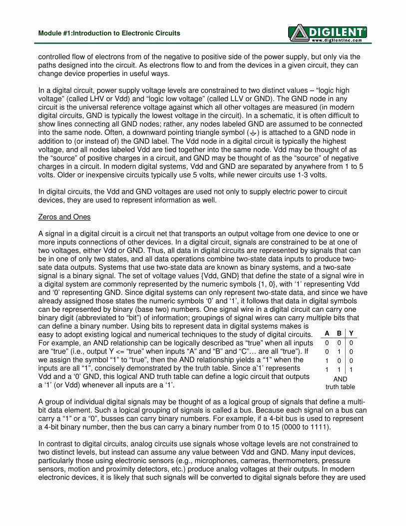
Output devices (LEDs) Circuits often require output devices to communicate their state to an user. Examples of electronic output devices include computer monitors, LCD alphanumeric panels (as on a calculator), small lamps or light-emitting diodes (LED's), etc. Digilent boards include different output devices, but all of them include some number of individual LED's, and seven-segment LED displays that can display the digits 0-9 in each digit position (each segment in the seven-segment display contains a single LED). LED's are two-terminal semiconductor devices that conduct current in only one direction (from the anode to the cathode). The small LED chips are secured inside a plastic housing, and they emit light at a given frequency (RED, YELLOW, etc.) when a small electric current (typically 10mA to 25mA) flows through them. Individual LED's are denoted with an "LD__" reference designator on Digilent boards, and seven-segment displays are denoted with a “DSP” reference designator. Individual LEDs are typically driven directly from a Xilinx chip on Digilent boards, but LED displays may require the use of an
Module #1:Introduction to Electronic Circuits
external transistor to supply higher currents to the digits. Typical LED circuits on Digilent boards are shown in the figure. LEDs will not turn on unless their anodes are some minimal voltage above their cathodes – typically about two volts. If less than the minimum threshold voltage is applied to an LED, it will remain dark. In the example shown, the LED requires a 2V drop to turn on, leaving 1.3V to drop across the resistor. Thus, a 130 ohm resistor is required to cause 10mA of current to flow in the circuit (3.3V – 2V = 1.3V, and 1.3V / 130 ohms = 10mA). Connectors The Digilent boards use several connectors for various purposes, but in general, they all communicate electronic information between the board and outside devices. By convention, connectors are given the reference designator "J__". Since connectors come in so many different sizes and shapes, they are usually shown on the PCB silk screen and on circuit schematics as just rectangular boxes. The following connectors are used on various Digilent boards (but not all connectors appear on all boards):
• The PS/2 connector allows connection to a mouse or keyboard;
• The DB25 connector allows a parallel cable to be attached for programming or data transfers;
• The DB9 port is used for RS-232 serial communications;
• The DB15 connector can be used to drive a VGA monitor;
• Various DIP sockets can be used to load accessory chips and to access various signals;
• The power jack can accept any compatible DC power supply;
• The audio jack can be used to drive speakers or receive microphone inputs;
• The BNC connector allows for easy connection of test and measurement equipment.
PS/2 connector "DB25" Parallel port D-connector
"DB9" Serial
port D-connector
HeadersDIP sockets Power jack
"DB15" VGA
D-connector
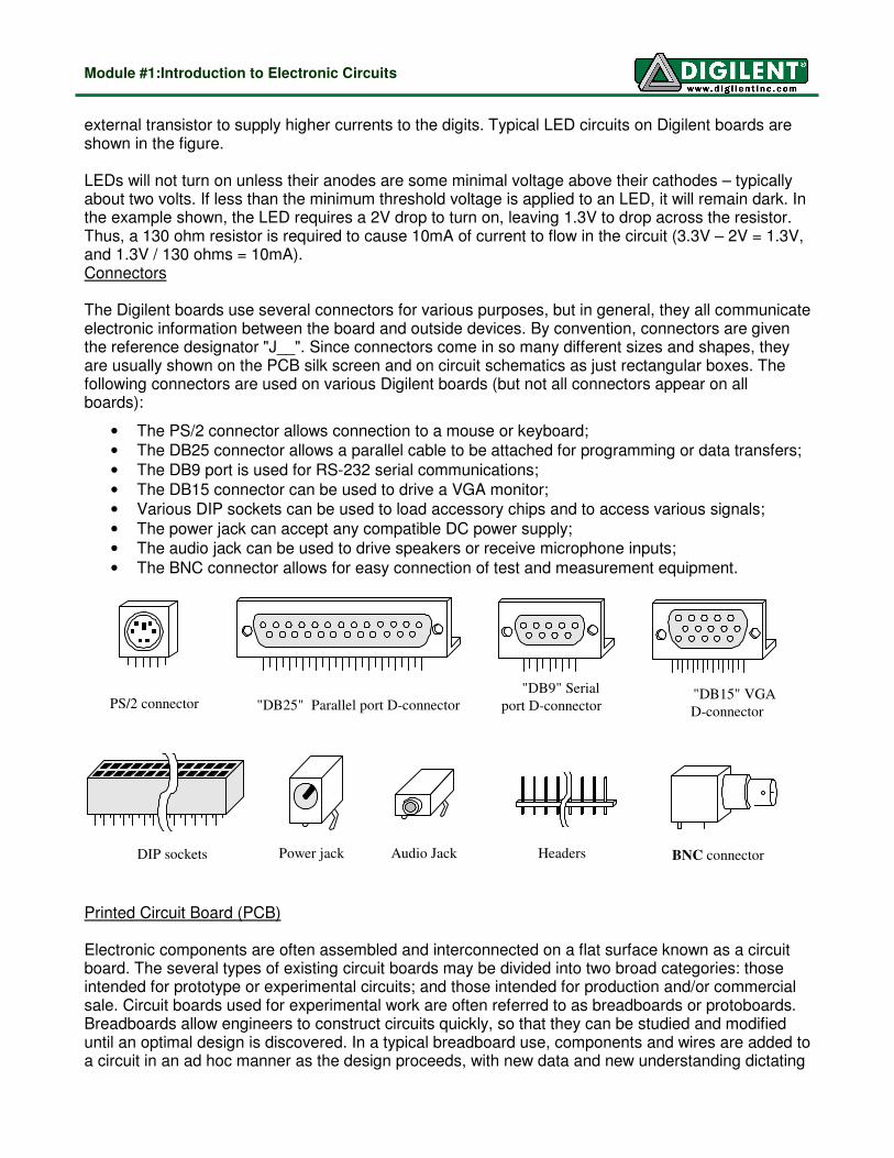
Audio Jack BNC connector Printed Circuit Board (PCB) Electronic components are often assembled and interconnected on a flat surface known as a circuit board. The several types of existing circuit boards may be divided into two broad categories: those intended for prototype or experimental circuits; and those intended for production and/or commercial sale. Circuit boards used for experimental work are often referred to as breadboards or protoboards. Breadboards allow engineers to construct circuits quickly, so that they can be studied and modified until an optimal design is discovered. In a typical breadboard use, components and wires are added to a circuit in an ad hoc manner as the design proceeds, with new data and new understanding dictating
Module #1:Introduction to Electronic Circuits
the course of the design. Since breadboard circuits exist only in the laboratory, no special consideration need be given to creating reliable or simple-to-manufacture circuits – the designer can focus exclusively on the circuit's behavior. In contrast, circuit boards intended for production or commercial sale must have highly reliable wires and interconnects, permanent bonds to all components, and topographies amenable to mass production and thorough testing. And further, they must be made of a material that is reliable, low-cost, and easy to manufacture. A fiberglass substrate with copper wires (etched from laminated copper sheets) has been the PCB material of choice for the past several decades. The Digilent board is a simple example of such a board. Note that most often, production circuit board designs are finalized only after extensive breadboard phases. Components are permanently affixed to production boards using the soldering process. Production circuit boards typically start out as thin sheets of fiberglass (about 1mm thick) that are completely covered on both sides with very thin sheets of metal (typically copper). A "standard" circuit board might use a 1 ounce copper process, which means that one ounce of copper is evenly spread across 1 square foot of circuit board. During the manufacturing process, wire patterns are "printed" onto the copper surfaces using a compound that resists etching (hence the name Printed Circuit Board or PCB). The boards are subjected to a chemical etching process that removes all exposed copper. The remaining, un-etched copper forms wires that will interconnect the circuit board components, and small pads that define the regions where component leads will be attached. In a PCB that uses through-hole technology, holes are drilled through the pads so that component leads can be inserted and then fastened (soldered) in place. In a PCB that uses surface-mount technology, component leads are soldered directly to the pads on the surface. Each set of pads (or holes) in the PCB is intended to receive a particular component. To identify which component must be loaded where, reference designators are printed on the circuit board immediately adjacent to the pads using a silk-screen process. A parts list links a designated set of pads to a physical component by describing the component and assigning it a particular reference designator. The reference designators guide assemblers and testers when they are working with the PCB. Many components must be placed into the PCB in a particular orientation. By convention, components that require a particular orientation have one lead designated as pin 1. On the PCB, a square pad or silkscreen indicator typically denotes pin 1. On all but the simplest PCBs, wires must be printed on more than one surface of fiberglass to allow for all the required component interconnections. Each surface containing printed wires is called a layer. In a relatively simple PCB that requires only two layers, only one piece of fiberglass is required since wires can be printed on both sides. In a more complex PCB where several layers are required, individual circuit boards are manufactured separately and then laminated together to form one multi-layer circuit board. To connect wires on two or more layers, small holes called vias are drilled through the wires and fiberglass board at the point where the wires on the different layers cross. The interior
PCB starts as a fiberglass sheet about 16" x 20" x .062"
Thin copper sheets are added to both sides
Etchant-resistive wire pattern printed on one or both sides
All copper removed with etchant except for wires and pads
Holes drilled for leads and vias, and plated with metal
Soldermask applied to keep solder only where needed

Module #1:Introduction to Electronic Circuits
surface of these holes is coated with metal so that electric current can flow through the vias. Most Digilent boards are simple four or six layer boards; some more complex computer circuit boards have more than 20 layers. The unloaded PCB appears green because thin sheets of green plastic have been applied to both sides (otherwise the PCB would appear pale yellow). Called solder masks, these sheets cover all exposed metal other than the component pads and holes so that errant solder can't inadvertently short (or electrically connect) the printed wires. All metal surfaces other than the exposed pads and holes (i.e., the wires) are underneath the solder mask. Not infrequently, blue or even red solder masks are used. Circuit components are manufactured with exposed metal pins (or leads) that are used to fasten them to the PCB both mechanically (so they won't fall off) and electrically (so current can pass between them). The soldering process, which provides a strong mechanical bond and a very good electrical connection, is used to fasten components to the PCB. During soldering, component leads are inserted through the holes in the PCB, and then the component leads and the through-hole plating metal are heated to above the melting point of the solder (about 500 to 700 degrees F). Solder (a metallic compound) is then melted and allowed to flow in and around the component lead and pad. The solder quickly cools to form a strong bond between the component and the PCB. The process of associating components with reference designators, loading them into their respective holes, and then soldering them in place comprises the PCB assembly process. Examine the Digilent board, and note the printed wires on either side. Wires on one side go largely "north and south" while wires on the other side go largely "east and west". The perpendicular or Manhattan arrangement of wires on alternate layers is very common on multi-layer PCBs. Locate some vias, and note that they connect wires on opposite sides. Locate various components, their hole patterns, and associated reference designators. Identify pad 1 for the various components. Note that the through-holes are somewhat larger than the vias, and that component leads can easily be inserted into their through-holes, but not into vias. Integrated Circuits (or Chips) The terms “chip” and “integrated circuit” refer to semiconductor circuits that use collections microscopic transistors that are all co-located on the same small piece of silicon. Chips have been designed to do all sorts of functions, from very simple and basic logical switching functions to highly complex processing functions. Some chips contain just a handful of transistors, while others contain several hundred million transistors. Some of the longest-surviving chips perform the most basic functions. These chips, denoted with the standard part numbers "74XXX", are simple small-scale integration devices that house small collections of logic circuits. For example, a chip known as a 7400 contains four individual NAND gates, with each input and output available at an external pin. As shown in the figures below, the chips themselves are much smaller than their packages. During manufacturing, the small, fragile chips are glued (using epoxy) onto the bottom half of the package, bond-wires are attached to the chip and to the externally available pins, and then the top half of the chip package is permanently affixed. Smaller chips may only have a few pins, but larger chips can have more than 500 pins. Since the chips themselves are on the order of a centimeter on each side, very precise and delicate machines are required to mount them in their packages. Smaller chips might be packaged in a "DIP" package (DIP is an acronym for Dual In-line Package) as shown below. Typically on the order of 1" x 1/4", DIP packages are most often made from black
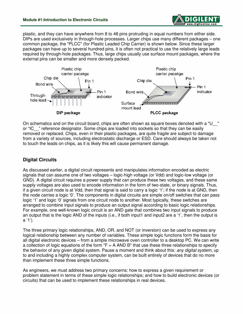
Module #1:Introduction to Electronic Circuits
plastic, and they can have anywhere from 8 to 48 pins protruding in equal numbers from either side. DIPs are used exclusively in through-hole processes. Larger chips use many different packages – one common package, the "PLCC" (for Plastic Leaded Chip Carrier) is shown below. Since these larger packages can have up to several hundred pins, it is often not practical to use the relatively large leads required by through-hole packages. Thus, large chips usually use surface mount packages, where the external pins can be smaller and more densely packed.
On schematics and on the circuit board, chips are often shown as square boxes denoted with a "U__" or “IC__” reference designator. Some chips are loaded into sockets so that they can be easily removed or replaced. Chips, even in their plastic packages, are quite fragile are subject to damage from a variety of sources, including electrostatic discharge or ESD. Care should always be taken not to touch the leads on chips, as it is likely this will cause permanent damage.
Digital Circuits As discussed earlier, a digital circuit represents and manipulates information encoded as electric signals that can assume one of two voltages – logic-high voltage (or Vdd) and logic-low voltage (or GND). A digital circuit requires a power supply that can produce these two voltages, and these same supply voltages are also used to encode information in the form of two-state, or binary signals. Thus, if a given circuit node is at Vdd, then that signal is said to carry a logic ‘1’; if the node is at GND, then the node carries a logic ‘0’. The components in digital circuits are simple on/off switches that can pass logic ‘1’ and logic ‘0’ signals from one circuit node to another. Most typically, these switches are arranged to combine input signals to produce an output signal according to basic logic relationships. For example, one well-known logic circuit is an AND gate that combines two input signals to produce an output that is the logic AND of the inputs (i.e., if both input1 and input2 are a ‘1’, then the output is a ‘1’). The three primary logic relationships, AND, OR, and NOT (or inversion) can be used to express any logical relationship between any number of variables. These simple logic functions form the basis for all digital electronic devices – from a simple microwave oven controller to a desktop PC. We can write a collection of logic equations of the form "F = A AND B" that use these three relationships to specify the behavior of any given digital system. Pause a moment and think about this: any digital system, up to and including a highly complex computer system, can be built entirely of devices that do no more than implement these three simple functions. As engineers, we must address two primary concerns: how to express a given requirement or problem statement in terms of these simple logic relationships; and how to build electronic devices (or circuits) that can be used to implement these relationships in real devices.

Module #1:Introduction to Electronic Circuits
Logic equations provide an abstract model of actual logic circuits. They are used to show how an output logic signal should be driven in response to changes on one or more input signals. The equal sign (“=”) is typically used as an assignment operator to indicate how information should flow through a logic circuit. For example, the simple logic equation “F = A” specifies that the output signal F should be assigned whatever voltage is currently on signal A, but this does not imply that F and A are the same circuit node – in fact, the use of a logic equation to specify circuit behavior implies that the inputs and outputs are separated by a circuit component. In digital circuits, circuit components act like one-way gates. Thus, the logic equation “F = A” dictates that a change on the signal A will result in a change on the signal F, but a change on F will not result in a change on A. Because of this directionality, assignment operators that indicate direction, such as “F <= A”, are often used. Most logic equations specify an output signal that is some function of input signals. For example, the logic equation “F <= A and B” specifies a logic circuit whose output will be driven to a ‘1’ only when both inputs are driven to a ‘1’. Below are six common logical functions written as conventional logic equations. The AND relationship, F = A·B, can be written without an operator between the A and B
(but more properly, a dot (⋅) should be placed between the variables to make the relationship clear). The OR relationship uses the plus sign, and the NOT or inversion relationship is shown by placing a bar over the inverted variable or by placing a single quote character after the variable or quantity to be inverted (two possible notations are shown for several relationships).
F = AB F = A + B F=A XOR B F = A BF = A F = A + B
F = A B F = A’ F = (A B)' F = (A + B)'F=A B
Compound logic expressions can be built from these basic functions. For example, an output might be need to driven to a ‘1’ if input signals A and B are both at ‘1’, or if input C is ‘0’, or if C is ‘1’ at the same time that A is ‘0’. This relationship can be concisely written as “F = AB + C’ +A’C”. A truth table is the primary tool for capturing logical relationships in a concise and universally understood format. All possible combinations of inputs are shown in rows on the left of a truth table, and outputs are shown on the right. A truth table with N inputs requires 2N rows to list all possible input combinations. A ‘0’ or ‘1’ in an output column of a given row specifies the behavior of the logic relationship for the combination of inputs shown in the adjacent row. For example, a truth table with two inputs, A and B, will require 22, or 4 rows to list all possible combinations: “0 0”, “0 1”, “1 0”, and “1 1”. For the ANDing operation, the output is “true” only when both inputs are true, so the rightmost column would have a ‘1’ only in the last row. For “F = A’ and B”, the truth table would have a ‘1’ only in the second row. In engineering, our goal is to produce electric circuits that can implement the behavior specified for any given logic relationship. For example, a design might require a warning light to be illuminated whenever sensor A outputs a logic 1, but only if sensor B also outputs a logic ‘1’ at the same time. In this example, perhaps the warning light is in an automobile dashboard, sensor A is a thermometer that outputs a ‘1’ if the temperature is above 90C, and sensor B outputs a ‘1’ if the coolant level is too low. If the coolant level ever becomes too low while the engine temperature too high, the circuit should “assert” its output, in order to do some work (like illuminating the warning light). We apply the same term to inputs – the AND relationship in this example may be stated as "the output F is asserted when the inputs A and B are both asserted". Some input signals to logic circuits might normally be a ‘0’, changing to ‘1’ only when some input device or circuit is activated (like the pushbuttons on the Basys board). Other input signals might normally be at ‘1’, changing to ‘0’ only when an input device is activated. In either case, we can use
Module #1:Introduction to Electronic Circuits
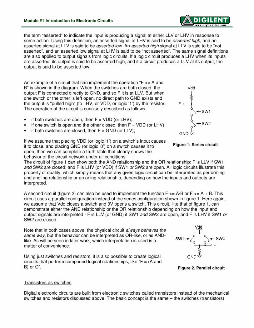
the term “asserted” to indicate the input is producing a signal at either LLV or LHV in response to some action. Using this definition, an asserted signal at LHV is said to be asserted high, and an asserted signal at LLV is said to be asserted low. An asserted high signal at LLV is said to be “not asserted”, and an asserted low signal at LHV is said to be “not asserted”. The same signal definitions are also applied to output signals from logic circuits. If a logic circuit produces a LHV when its inputs are asserted, its output is said to be asserted high, and if a circuit produces a LLV at its output, the output is said to be asserted low. An example of a circuit that can implement the operation “F <= A and B” is shown in the diagram. When the switches are both closed, the output F is connected directly to GND, and so F it is at LLV. But when one switch or the other is left open, no direct path to GND exists and the output is "pulled high" (to LHV, or VDD, or logic ‘1’) by the resistor. The operation of the circuit is concisely described as follows:
• if both switches are open, then F = VDD (or LHV);
• if one switch is open and the other closed, then F = VDD (or LHV);
• if both switches are closed, then F = GND (or LLV); If we assume that placing VDD (or logic ‘1’) on a switch’s input causes it to close, and placing GND (or logic ‘0’) on a switch causes it to open, then we can complete a truth table that clearly shows the behavior of the circuit network under all conditions. The circuit of figure 1 can show both the AND relationship and the OR relationship: F is LLV if SW1 and SW2 are closed; and F is LHV (or VDD) if SW1 or SW2 are open. All logic circuits illustrate this property of duality, which simply means that any given logic circuit can be interpreted as performing and and’ing relationship or an or’ing relationship, depending on how the inputs and outputs are interpreted. A second circuit (figure 2) can also be used to implement the function F <= A·B or F <= A + B. This circuit uses a parallel configuration instead of the series configuration shown in figure 1. Here again, we assume that Vdd closes a switch and 0V opens a switch. This circuit, like that of figure 1, can demonstrate either the AND relationship or the OR relationship depending on how the input and output signals are interpreted - F is LLV (or GND) if SW1 and SW2 are open, and F is LHV if SW1 or SW2 are closed. Note that in both cases above, the physical circuit always behaves the same way, but the behavior can be interpreted as OR-like, or as AND-like. As will be seen in later work, which interpretation is used is a matter of convenience. Using just switches and resistors, it is also possible to create logical circuits that perform compound logical relationships, like “F = (A and B) or C”. Transistors as switches Digital electronic circuits are built from electronic switches called transistors instead of the mechanical switches and resistors discussed above. The basic concept is the same – the switches (transistors)
Figure 2. Parallel circuit
Vdd
GND
F
SW1
SW2
Figure 1: Series circuit

Module #1:Introduction to Electronic Circuits
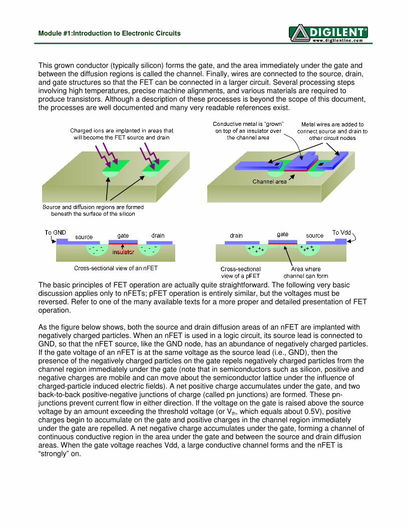
are arranged so that they can be turned on or off by signals carrying either LLV or LHV. The transistor switches used in modern digital circuits are called “Metal Oxide Semiconductor Field Effect Transistors”, or MOSFETs (or just FETs). FETs are three terminal devices that can conduct current between two terminals (the source and the drain) when a third terminal (the gate) is driven by an appropriate logic signal. In the simplest FET model (which is appropriate for our use here), the electrical resistance between the source and the drain is a function of the gate-to-source voltage – the higher the gate voltage, the lower the resistance (and therefore, the more current that can flow). In analog circuits (like audio amplifiers), the gate-to-source voltage is allowed to assume any voltage between GND and Vdd; but in digital circuits, the gate-to-source voltage is constrained to be either Vdd or GND (of course, when the gate voltage changes from Vdd to GND or vice-versa, it must necessary assume voltages between Vdd and GND – we assume that this happens infinitely fast, so that we can ignore FET characteristics during the time the gate voltage is switching). In a simple digital model, FETs can be thought of as electrically controllable "on/off" switches. An electrical connection is created between the source and the drain (i.e., the FET is turned “on”) when the gate input is asserted. One kind of FET, called an nFET, is turned on when Vdd is present at the control input, and a second type, called a pFET, is turned on when GND is present at the control input. Thus, an "asserted" input for an nFET means that the control signal is at Vdd, and for a pFET means the control input is at a GND. The figures below show the circuit symbols and equivalent switch diagrams for both nFETs and pFETs. Individual FETs are often used as stand-alone electrically controllable on-off switches. As an example, an nFET can be used to turn on and off an appliance if a power source is connected to the source and the load (such as a motor, lamp, or other electrical component in an appliance) is connected to the drain. A signal applied to the gate could then turn the load device on (gate = GND) or off (gate = Vdd). Typically, a relatively small voltage (on the order of a few volts) is required to turn on a FET, even if the FET is switching large voltages and currents. Individual FETs used for this purpose are typically rather large (macroscopic) devices. FETs can also be arranged into circuits that perform useful logic functions such as AND, OR, NOT, etc. In this application, several very small FETs are constructed on a single small piece of silicon (or chip of silicon) and then interconnected with equally small metal wires. These microscopic FETs typically occupy an area of less than 1 x 10e-7m2. Since a silicon chip might measure several millimeters on a side, several millions of FETs can be constructed on a single chip. Circuits assembled in this fashion are said to form "integrated circuits" (or IC’s), because all circuit components are constructed and integrated on the same piece of silicon. Most FETs are manufactured using the semi-conductor silicon. During manufacturing, a silicon chip is implanted with ions to make it more conductive in the areas that will become the FET source and the drain regions – these regions are commonly called diffusion regions. Next, a thin insulating layer is created between these diffusion regions, and another conductor is "grown" on top of this insulator.
gatenFET
drain
source
drain
Vdd
source
drain
Open
GND
Vgate = Vdd Vgate = GND
Closed
Symbol
source
drain
gate
source source
drain
Vdd
pFET
source
drain
GND
Closed Open
Module #1:Introduction to Electronic Circuits
This grown conductor (typically silicon) forms the gate, and the area immediately under the gate and between the diffusion regions is called the channel. Finally, wires are connected to the source, drain, and gate structures so that the FET can be connected in a larger circuit. Several processing steps involving high temperatures, precise machine alignments, and various materials are required to produce transistors. Although a description of these processes is beyond the scope of this document, the processes are well documented and many very readable references exist.
The basic principles of FET operation are actually quite straightforward. The following very basic discussion applies only to nFETs; pFET operation is entirely similar, but the voltages must be reversed. Refer to one of the many available texts for a more proper and detailed presentation of FET operation. As the figure below shows, both the source and drain diffusion areas of an nFET are implanted with negatively charged particles. When an nFET is used in a logic circuit, its source lead is connected to GND, so that the nFET source, like the GND node, has an abundance of negatively charged particles. If the gate voltage of an nFET is at the same voltage as the source lead (i.e., GND), then the presence of the negatively charged particles on the gate repels negatively charged particles from the channel region immediately under the gate (note that in semiconductors such as silicon, positive and negative charges are mobile and can move about the semiconductor lattice under the influence of charged-particle induced electric fields). A net positive charge accumulates under the gate, and two back-to-back positive-negative junctions of charge (called pn junctions) are formed. These pn-junctions prevent current flow in either direction. If the voltage on the gate is raised above the source voltage by an amount exceeding the threshold voltage (or Vth, which equals about 0.5V), positive charges begin to accumulate on the gate and positive charges in the channel region immediately under the gate are repelled. A net negative charge accumulates under the gate, forming a channel of continuous conductive region in the area under the gate and between the source and drain diffusion areas. When the gate voltage reaches Vdd, a large conductive channel forms and the nFET is “strongly” on.

Module #1:Introduction to Electronic Circuits
As the following figure shows, nFETs used in logic circuits have their source leads attached to GND and Vdd on their gate turns them on, while pFETs have their source leads attached to Vdd and GND on their gate turns them on.
For reasons that will become clear later, an nFET with its source attached to Vdd will not turn on very strongly, so nFET sources are rarely connected to Vdd. Similarly, a pFET with its source attached to GND will not turn on very well either, so pFETs are rarely connected to GND. Logic circuits built from FETs Armed only with this basic description of FET operation, it is possible to construct the basic logic circuits that form the backbone of all digital and computer circuits. These logic circuits will combine one or more input signals to produce an output signal according to the logic function requirements. The following discussion is restricted to circuits for basic logic functions (like AND, OR, and INV), but FET circuits can readily be built for more complex logic circuits as well. When building FET circuits to implement logic relationships, four basic rules must be followed: • pFET sources must be connected to Vdd and nFET sources must be connected to GND; • the circuit output must always be connected to Vdd via an on pFET or to GND via an on nFET
(i.e., the circuit output must never be left floating); • the logic circuit output must never be connected to both Vdd and GND at the same time (i.e., the
circuit output must not be “shorted”); • the circuit must use the fewest possible number of FETs. Following these rules, a circuit that can form the AND relationship between two input signals is developed. But first, note that in the circuit on the right, the output (labeled Y) is connected to GND only if the two inputs A and B are at Vdd. The two nFETs labeled Q1 and Q2 are said to be in series; in general, a series connection of FETs is required for an AND function. In the
A
B
Y
AQ1
Q2
Series configuration:
Y = LLV if A and B are LHV
Q3 Q4B
Y
Parallel configuration:
Y = LLV if A or B are LHV

Module #1:Introduction to Electronic Circuits
circuit on the right below, the output Y is connected to GND if A or B are at Vdd. The two nFETs labeled Q3 and Q4 are said to be in parallel; in general, a parallel connection of FETs is required for an OR function. Keeping in mind the rules for FET logic circuits, an AND structure is created from Q1 and Q2 below. Using just these two FETs, Y is driven to GND whenever A and B are at Vdd. But we must also ensure the output Y is at Vdd when A and B are not both at Vdd; restated, we must ensure the output Y is at Vdd whenever A or B are at GND. This can be accomplished with an OR'ing structure of pFETs (Q3 and Q4 below). The AND'ing structure and OR'ing structure are assembled in the circuit on the right below. The adjacent operation table shows the input and output voltages for all four possible combinations of inputs. Note that this circuit obeys all the rules above – pFETs are connected only to Vdd, nFETs are connected only to ground, the output is always driven to Vdd or to GND but never to both simultaneously, and the fewest possible number of FETs are used.
This AND’ing circuit has the interesting property of producing an output signal at GND when both inputs A and B are at Vdd. In order to have this circuit's performance match the AND logical truth table above, we must associate an input signal at Vdd with a logic 1 (and therefore, an input signal at GND must be associated with a logic 0); and we must associate an output signal at GND with a logic 1. This creates a potentially confusing situation – considering the “1” symbol to represent a signal at Vdd on the input of a gate, and then considering that same “1” symbol to represent a signal at GND on the output of a gate. Note that if the outputs in the Y column of the truth table were inverted (that is, if Vdd were changed to GND and GND were changed to Vdd), then a “1” symbol could represent Vdd for both the inputs and outputs, resulting in the AND truth table presented earlier. Because of this, the circuit shown above is called a NOT AND gate (were NOT means inversion), which is shortened to “NAND” gate. To create an AND circuit in which both the input signals and output signals can associate a Vdd signal with a logic “1”, an inverter circuit must be added to the output of the NAND gate (as the name implies, an inverter produces a Vdd output for a GND input, and vice-versa). Shown below are the five basic logic circuits: NAND, NOR (for “NOT OR”), AND, OR and INV (for inverter). The reader should verify that all truth tables show the correct circuit operation. These basic logic circuits are frequently referred to as logic gates. In each of these logic gates, a minimum number of FETs has been used to produce the required logic function. Each
pFETs
nFETs
Vdd
Output
Inputs

Module #1:Introduction to Electronic Circuits
circuit has nFETs "on the bottom" and pFETs "on the top" performing complementary operations; that is, when an OR relationship is present in the nFETs, an AND relationship is present in the pFETs. FET circuits that exhibit this complementary nature are called Complementary Metal Oxide Semiconductor, or CMOS, circuits. CMOS circuits are by far the dominant circuits used today in digital and computer circuits. (Incidentally, the Metal-Oxide-Semiconductor name refers to older technologies where the gate material was made of metal and the insulator beneath the gate made of silicon oxide). These basic logic circuits form the basis for all digital and computer circuits.
CMOS NANDCMOS INVERTER
A B FA
BF
Vdd
A F
VddA
B
F
Vdd
L
L
H
H
L
H
L
H
H
H
H
L
CMOS NOR
A B F
L
L
H
H
L
H
L
H
H
L
L
L
A F
L
H
H
L
CMOS AND
A B F
L
L
H
H
L
H
L
H
L
L
L
H
A B F
L
L
H
H
L
H
L
H
L
H
H
H
CMOS OR
A
B
Vdd
F
A
B
Vdd
F
When these circuits are used in schematic drawings, the well-known symbols shown below are used rather than the FET circuit diagrams (it would simply be too tedious to draw the FET circuits). A straight edge on the input side of a symbol and smoothly curved output side means AND, while a curved edge on the input side and pointed output side means OR. A bubble on an input means that input must be at LLV to produce the indicated logic function output, and a bubble on the output means that a LLV output signal is produced as a result of the logic function. The lack of a bubble on inputs means that signals must be at LHV to produce the indicated function, and the lack of a bubble on the output means that a LHV signal is produced as a result of the logic function.
INV NAND NOR AND OR
Note that each of the symbols above has two appearances. The symbols on the top may be considered the primary symbols, and those on the bottom may be considered the conjugate symbols (properly, each symbol is the conjugate of the other). Conjugate symbols swap AND and OR shapes, and input and output assertion levels. The reader should verify that both symbols are appropriate for

Module #1:Introduction to Electronic Circuits
the underlying CMOS circuit. For example, the AND shaped symbol for the NAND circuit shows that if two inputs A and B are at LVH, then the output is at LLV. The OR shaped symbol for the NAND circuit shows that if either of two input A and B are at LLV, then the output is at LHV. Both statements are true, illustrating that any logic gate can be thought of in conjugate forms. (Why conjugate forms? In certain settings, it can be easier for humans to follow circuit schematics if the appropriate symbol is used – more on this later). Logic Circuit Schematics Digital logic circuits can be built from individual logic chips, or from resources available on larger chips (like the user-programmable Xilinx chip on the Basys board). Regardless of how logic circuits are implemented, they can be fully specified by truth tables, logic equations, or schematics. This section will present the preparation and reading of logic circuit schematics. A later lab will explore the relationships between circuits and truth tables. A circuit schematic for any logic equation can be easily created by substituting logic gate symbols for logical operators, and by showing inputs as signal wires arriving at the logic gates. Perhaps the only step requiring some thought is in deciding which logic operation (and therefore, which logic gate) drives the output signal, and which logic operations drive internal circuit nodes. Any confusion can be avoided if parenthesis are used liberally in logic equations to show operator precedence, of if rules of precedence are established. For example, a schematic for the logic equation “F <= A.B + C.B” might use an OR gate to drive the output signal F, and two AND gates to drive the OR gate inputs, or it might use a three-input AND gate to drive F, with AND inputs coming from the A and B signals directly and a “B + C” OR gate. If no parentheses are used, then NAND/AND has the highest precedence, followed XOR, then NOR/OR, and finally INV. In general, it is easiest to sketch circuits from logic equations if the output gate is drawn first. Inverters can be used in logic equations to show that an input signal must be inverted prior to driving a logic gate. For example, a schematic for “F <= A’B + C” would use an inverter on the A input prior to a 2-input AND gate. Equations may also show that the output of a logic function must be inverted – in this case, an inverter can be used, or the preceding circuit symbol can show an inverted output (i.e., the preceding symbol can show an output bubble). The figure on the right shows an example.
"F = (A.B)' + C'.B" can be implemented in two different ways as shown
A
B
C
F
A
B
C
F
A
B
C
FB
C
A
B
F
"F = A.B + C.B" can be interpreted in two different ways as shown

Module #1:Introduction to Electronic Circuits
Reading logic equations from schematics is straightforward. The logic gate that drives the output signal defines the “major” logic operation, and it can be used to determine how other terms must be grouped in the equation. An inverter, or an output bubble on a logic gate, requires that the inverted signal or function output be shown in the output of the “downstream” gate (see example below). A bubble on the input of a logic gate can be thought of as an inverter on the signal leading to the gate.
(A.B)'A
B
C
F = (A.B)' + C'.B
C'.B
(A.B)'A
B
C
F = (A.B) + (C'.B)'
C'.B
Input bubbles also cause inversion
Two “back-to-back” signal inversions cancel each other. That is, if a signal is inverted, and immediately inverted again before it is used anywhere else, then the circuit would perform identically if both inversions were simply removed. This observation can be used to simplify circuits, or to make them more efficient. As an example, consider the circuits below, both of which perform identical logic functions. The circuit on the right has been simplified by removing the two inverters on signal C, and made more efficient by adding inversions on internal nodes so that NAND gates (at four transistors each) could be used instead of AND/OR gates (at six transistors each).
A
B
C
F = A.B + C.B
22 transistors
A
B
C
F = A.B + C.B
12 transistors