Embed Size (px)
Citation preview
MICROPROCESSOR 8085
MODULE 1
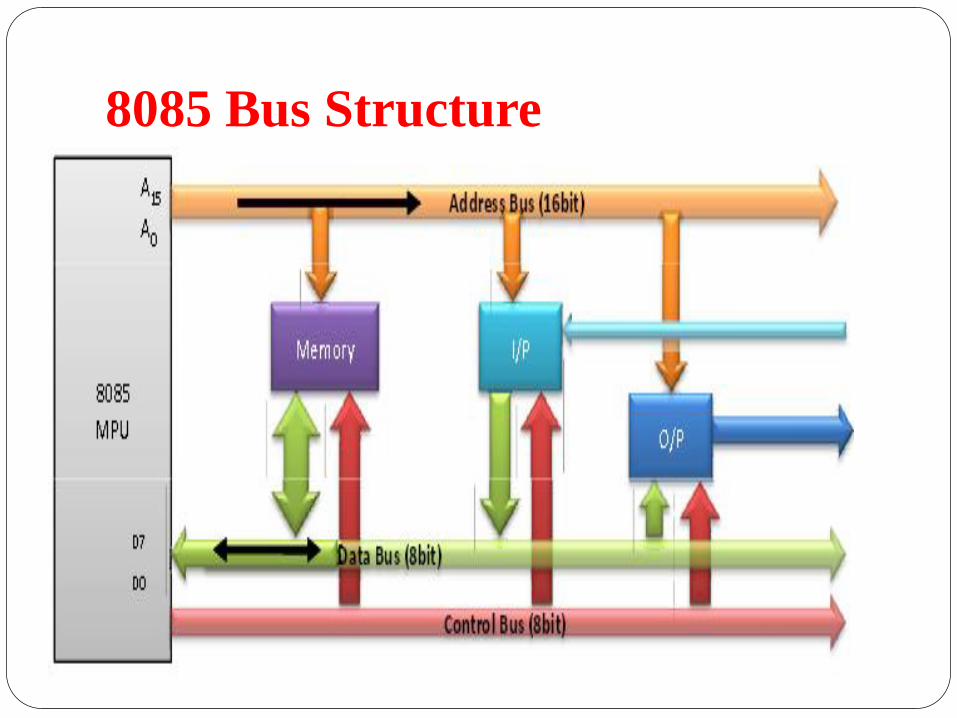
8085 Bus Structure
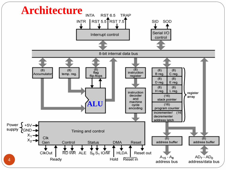
Architecture
4
ALU
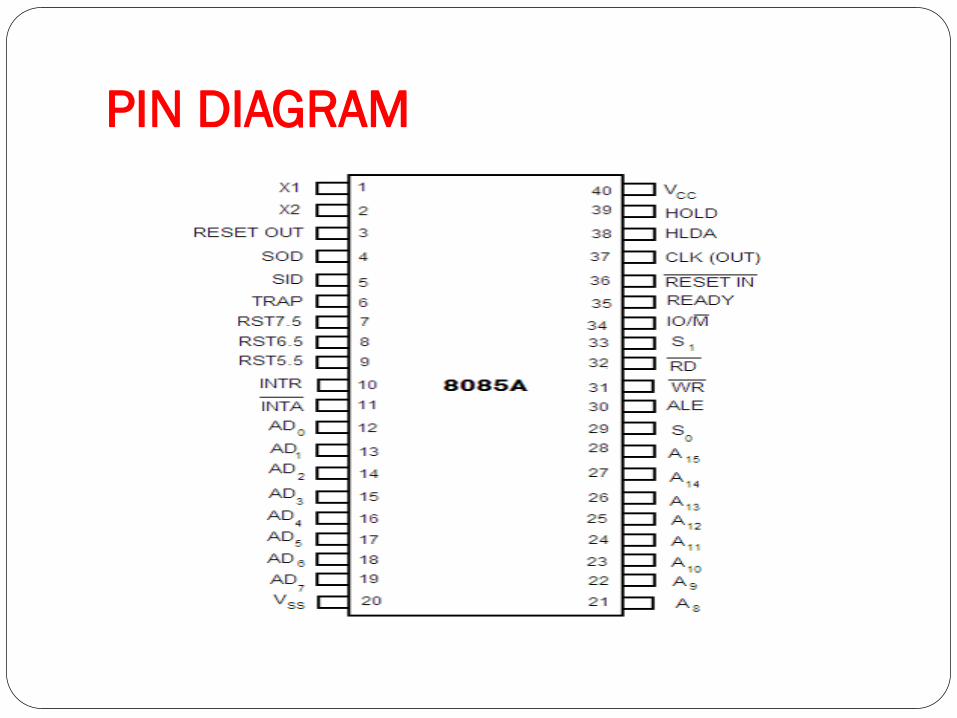
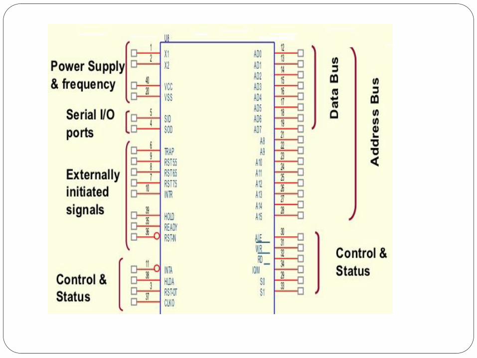
PIN DIAGRAM
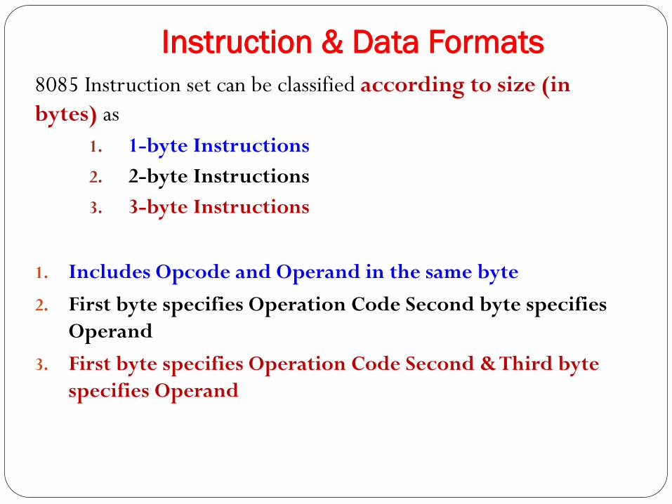
Instruction & Data Formats
8085 Instruction set can be classified according to size (in
bytes) as
1. 1-byte Instructions
2. 2-byte Instructions
3. 3-byte Instructions
1. Includes Opcode and Operand in the same byte
2. First byte specifies Operation Code Second byte specifies
Operand
3. First byte specifies Operation Code Second & Third byte
specifies Operand
Instruction & Data Formats1. 1-byte Instructions
Eg. MOV A, M, CMA, DAA etc
2. 2-byte Instructions
Eg. MVI A, 08, IN 02, CPI 03 etc
3. 3-byte Instructions
Eg. LXI H, 4500, STA 4600, LDA 4200
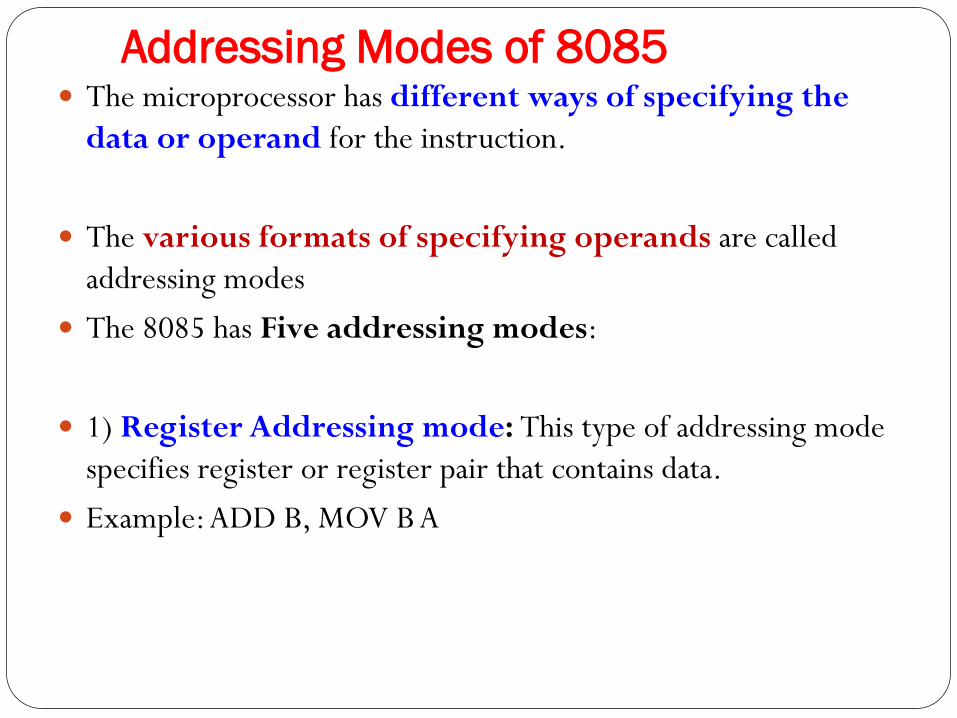
Addressing Modes of 8085 The microprocessor has different ways of specifying the
data or operand for the instruction.
The various formats of specifying operands are called
addressing modes
The 8085 has Five addressing modes:
1) Register Addressing mode: This type of addressing mode
specifies register or register pair that contains data.
Example: ADD B, MOV B A
Addressing Modes of 8085
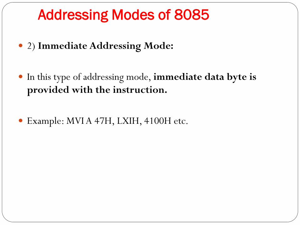
2) Immediate Addressing Mode:
In this type of addressing mode, immediate data byte is
provided with the instruction.
Example: MVI A 47H, LXIH, 4100H etc.
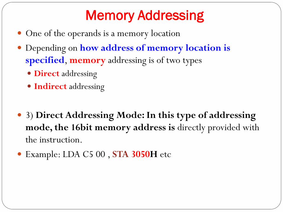
Memory Addressing
One of the operands is a memory location
Depending on how address of memory location is
specified, memory addressing is of two types
Direct addressing
Indirect addressing
3) Direct Addressing Mode: In this type of addressing
mode, the 16bit memory address is directly provided with
the instruction.
Example: LDA C5 00 , STA 3050H etc
Addressing Modes of 8085
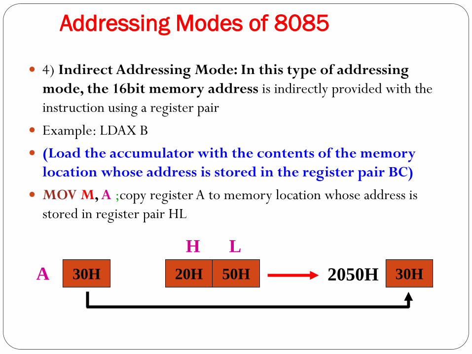
4) Indirect Addressing Mode: In this type of addressing
mode, the 16bit memory address is indirectly provided with the
instruction using a register pair
Example: LDAX B
(Load the accumulator with the contents of the memory
location whose address is stored in the register pair BC)
MOV M, A ;copy register A to memory location whose address is
stored in register pair HL
30HA 20H
H
50H
L
30H2050H
Addressing Modes of 8085
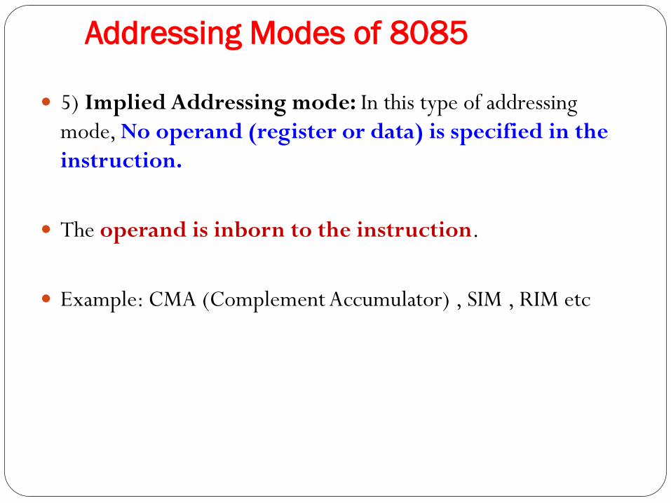
5) Implied Addressing mode: In this type of addressing
mode, No operand (register or data) is specified in the
instruction.
The operand is inborn to the instruction.
Example: CMA (Complement Accumulator) , SIM , RIM etc
INSTRUCTION SET
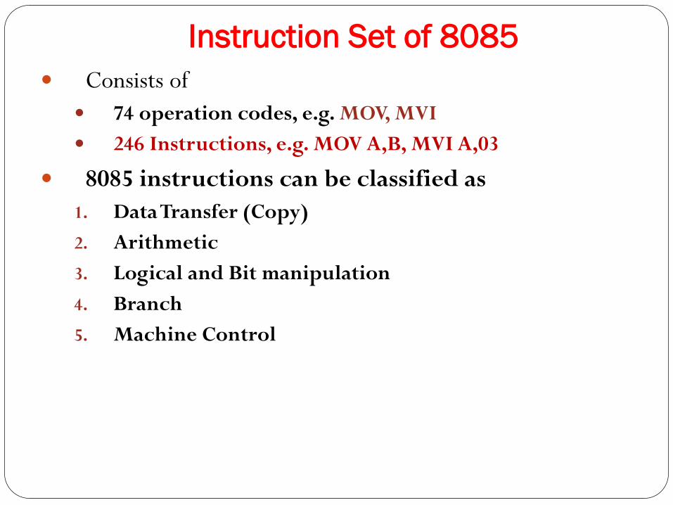
Instruction Set of 8085
Consists of
74 operation codes, e.g. MOV, MVI
246 Instructions, e.g. MOV A,B, MVI A,03
8085 instructions can be classified as
1. Data Transfer (Copy)
2. Arithmetic
3. Logical and Bit manipulation
4. Branch
5. Machine Control
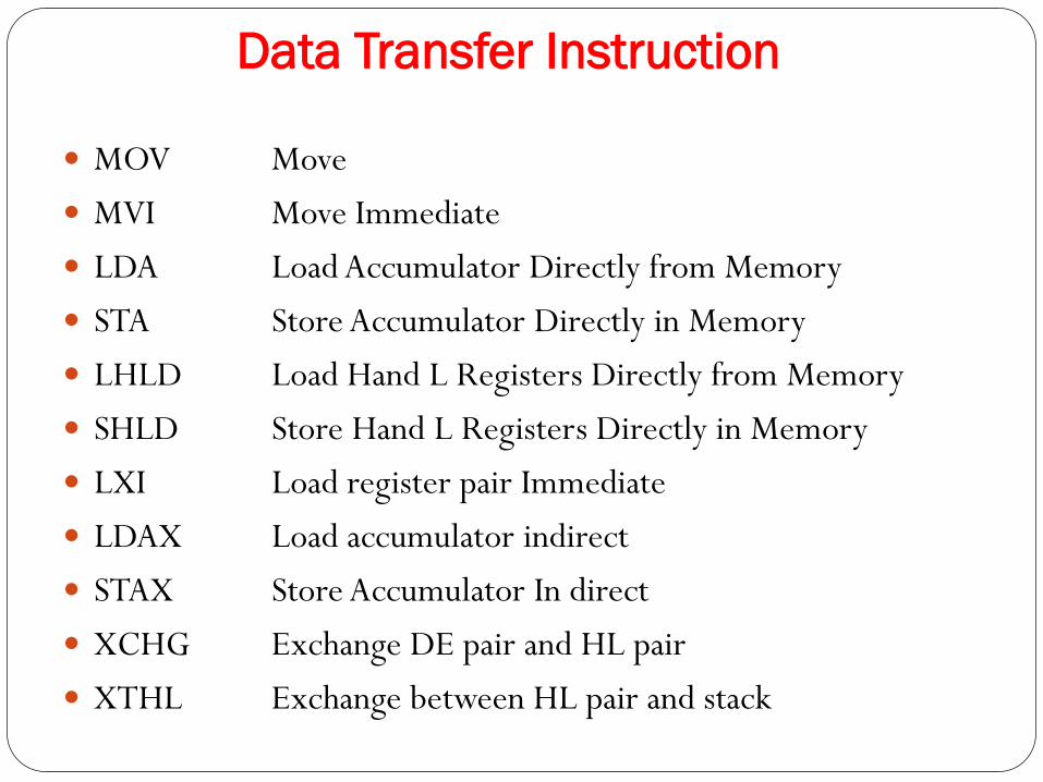
Data Transfer Instruction
MOV Move
MVI Move Immediate
LDA Load Accumulator Directly from Memory
STA Store Accumulator Directly in Memory
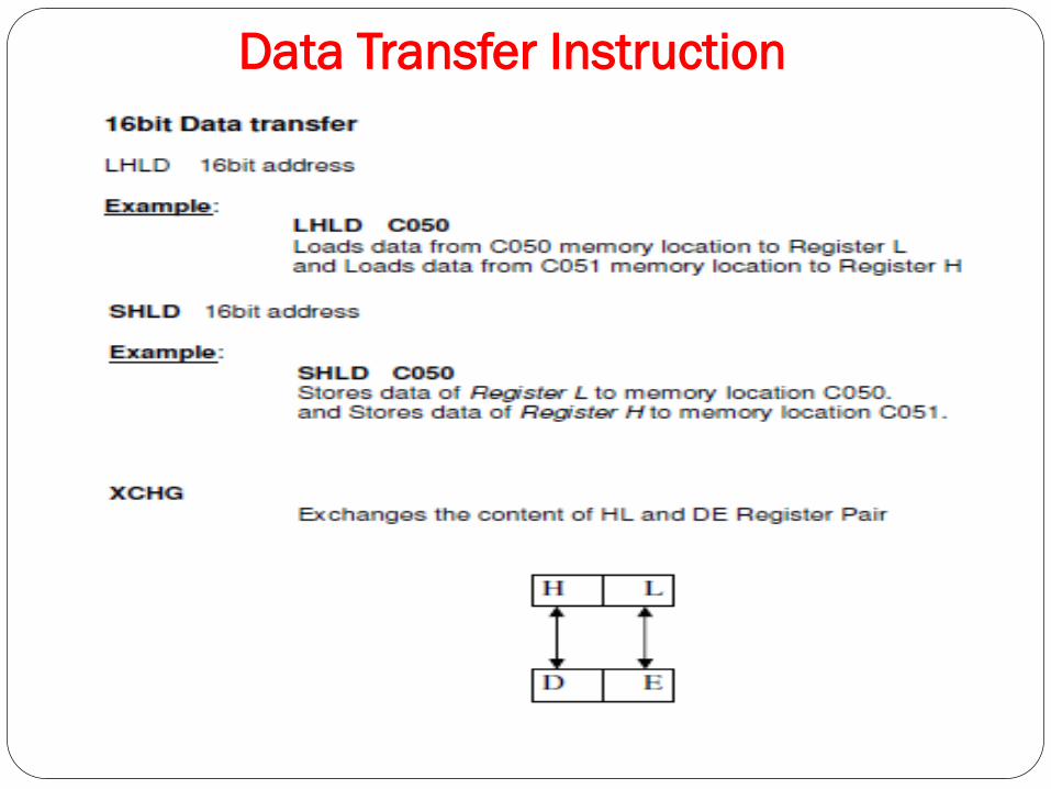
LHLD Load Hand L Registers Directly from Memory
SHLD Store Hand L Registers Directly in Memory
LXI Load register pair Immediate
LDAX Load accumulator indirect
STAX Store Accumulator In direct
XCHG Exchange DE pair and HL pair
XTHL Exchange between HL pair and stack
Data Transfer Instruction
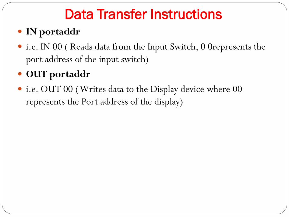
Data Transfer Instructions IN portaddr
i.e. IN 00 ( Reads data from the Input Switch, 0 0represents the
port address of the input switch)
OUT portaddr
i.e. OUT 00 ( Writes data to the Display device where 00
represents the Port address of the display)
Arithmetic Instructions
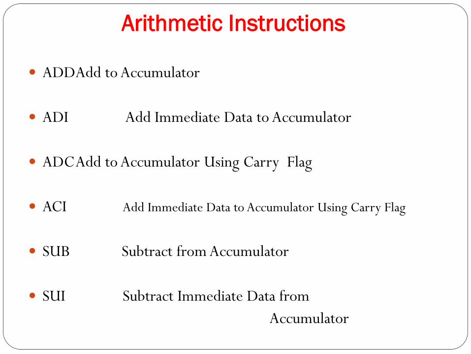
ADDAdd to Accumulator
ADI Add Immediate Data to Accumulator
ADCAdd to Accumulator Using Carry Flag
ACI Add Immediate Data to Accumulator Using Carry Flag
SUB Subtract from Accumulator
SUI Subtract Immediate Data from
Accumulator
Arithmetic Instructions
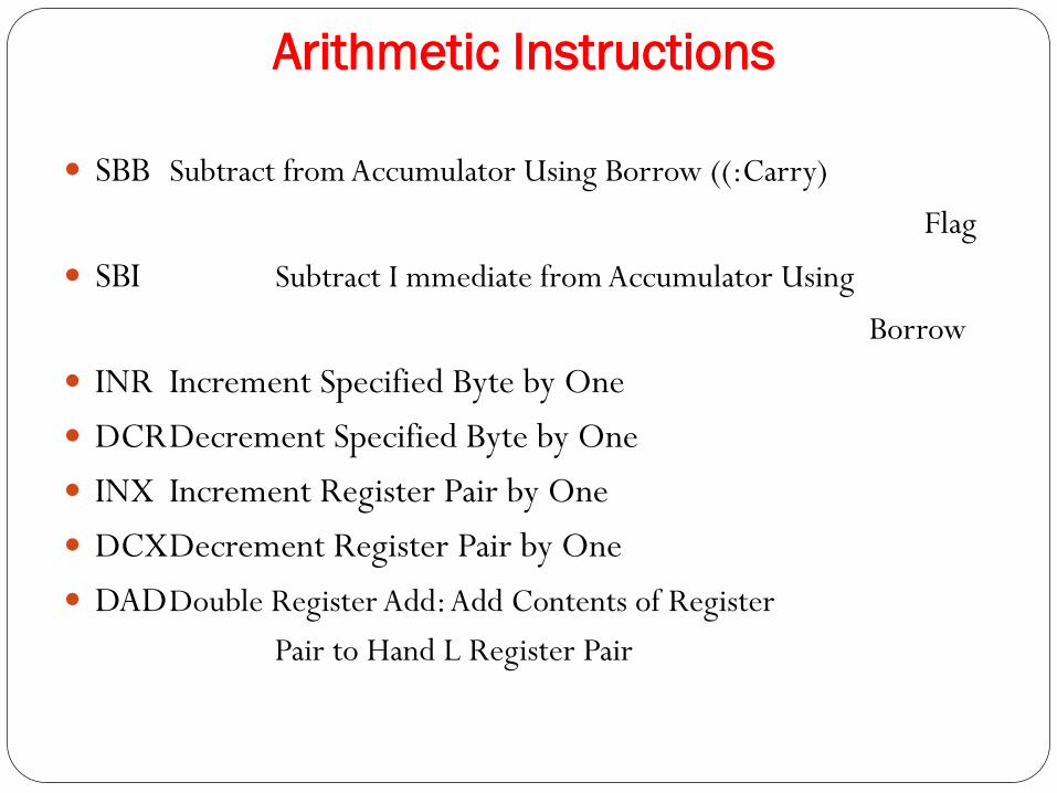
SBB Subtract from Accumulator Using Borrow ((:Carry)
Flag
SBI Subtract I mmediate from Accumulator Using
Borrow
INR Increment Specified Byte by One
DCRDecrement Specified Byte by One
INX Increment Register Pair by One
DCXDecrement Register Pair by One
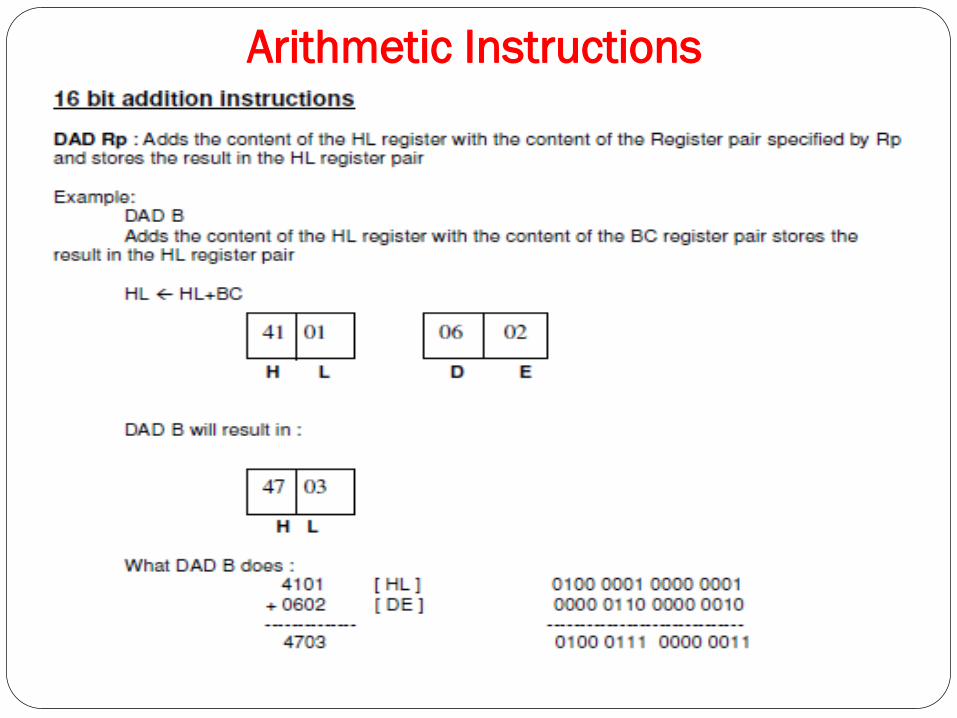
DADDouble Register Add: Add Contents of Register
Pair to Hand L Register Pair
Arithmetic Instructions
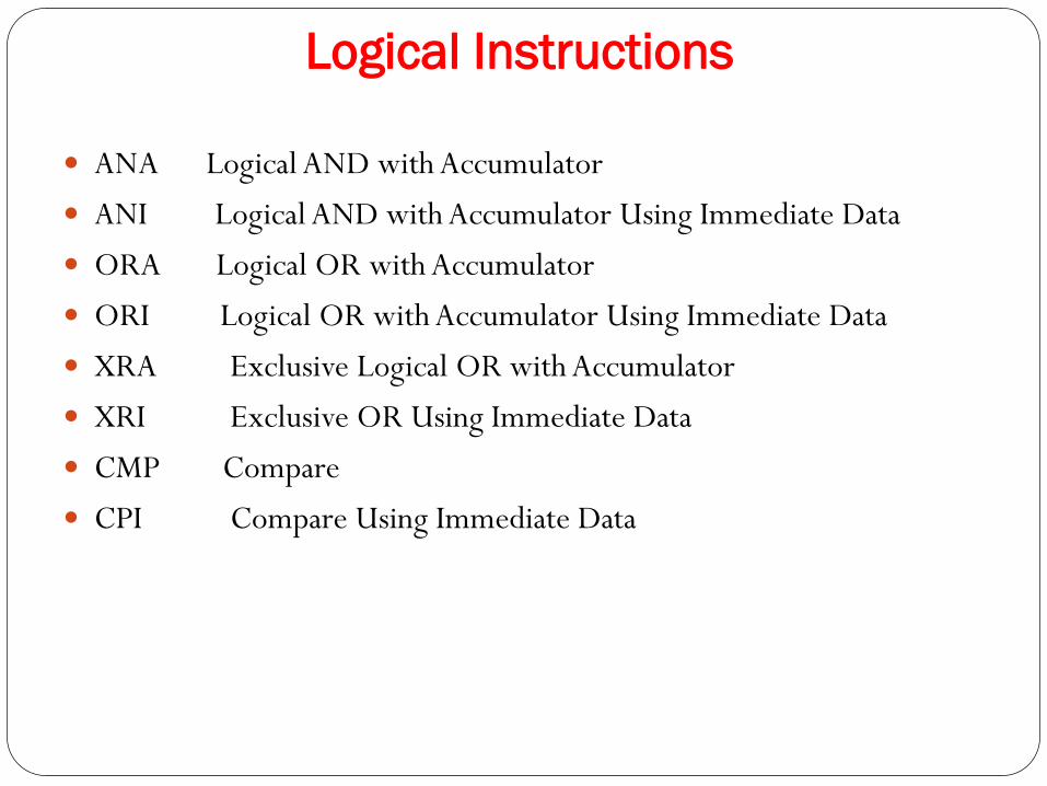
Logical Instructions
ANA Logical AND with Accumulator
ANI Logical AND with Accumulator Using Immediate Data
ORA Logical OR with Accumulator
ORI Logical OR with Accumulator Using Immediate Data
XRA Exclusive Logical OR with Accumulator
XRI Exclusive OR Using Immediate Data
CMP Compare
CPI Compare Using Immediate Data
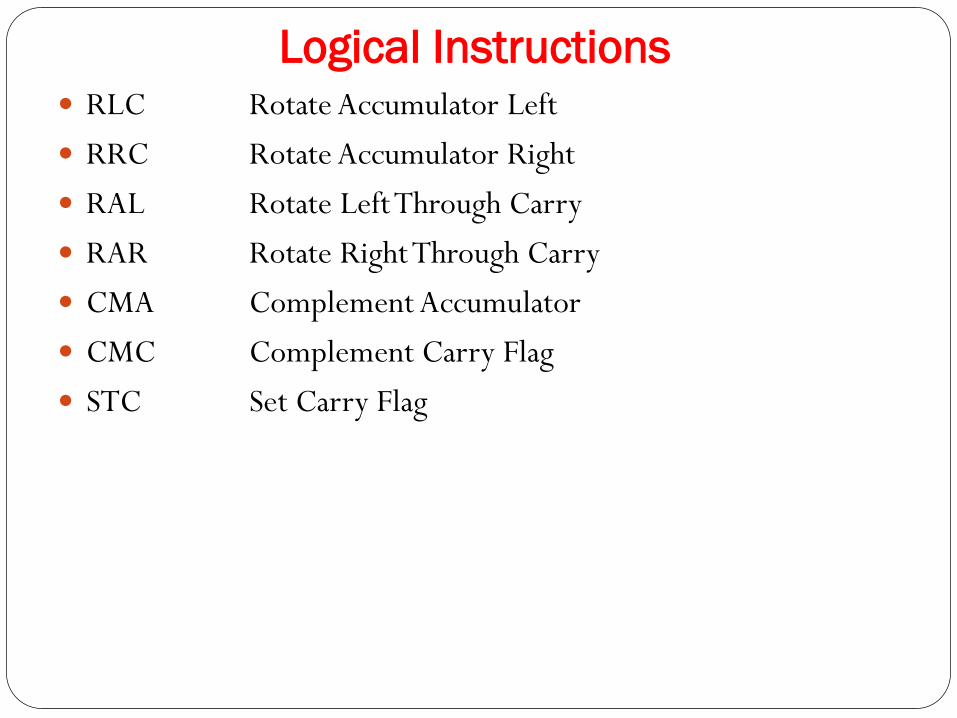
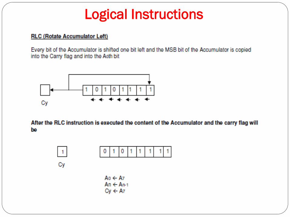
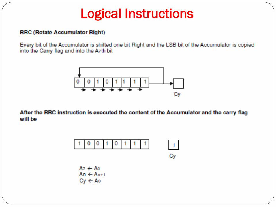
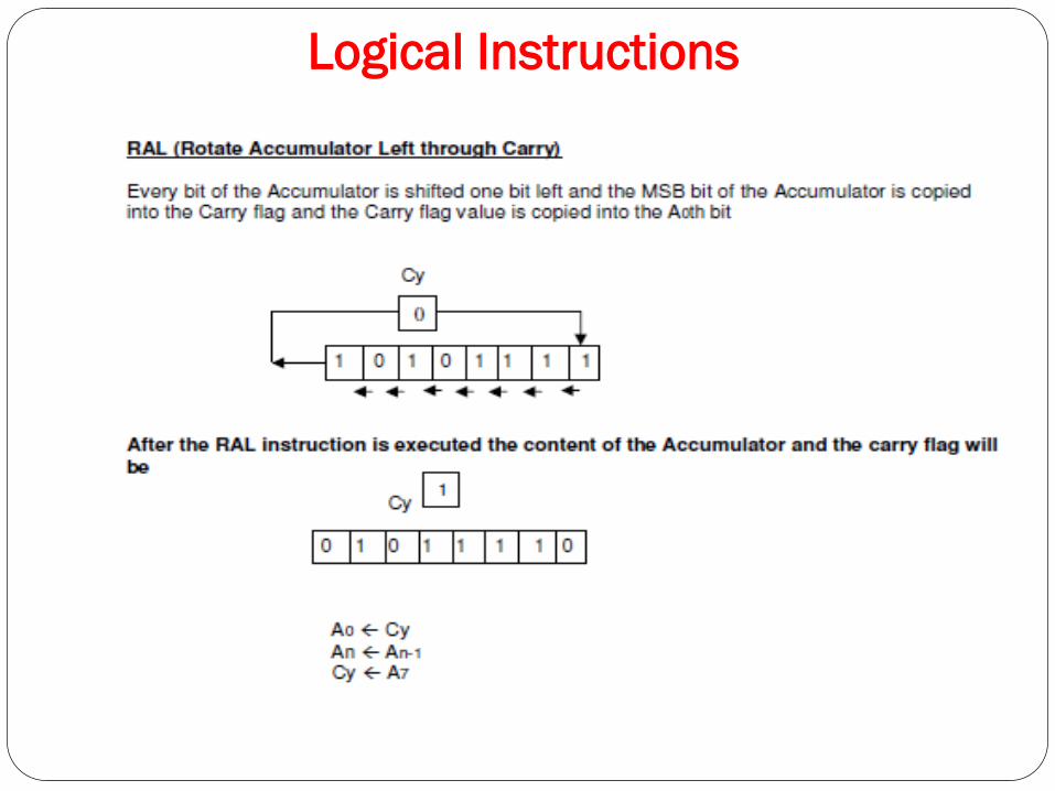
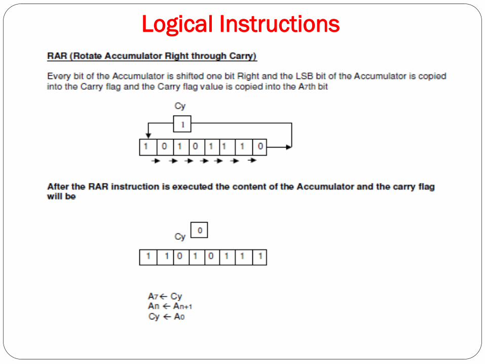
Logical Instructions RLC Rotate Accumulator Left
RRC Rotate Accumulator Right
RAL Rotate Left Through Carry
RAR Rotate Right Through Carry
CMA Complement Accumulator
CMC Complement Carry Flag
STC Set Carry Flag
Logical Instructions
Logical Instructions
Logical Instructions
Logical Instructions
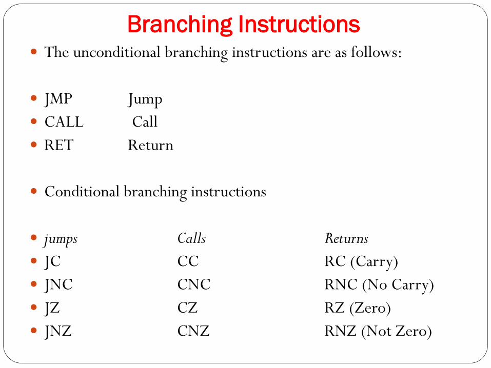
Branching Instructions The unconditional branching instructions are as follows:
JMP Jump
CALL Call
RET Return
Conditional branching instructions
jumps Calls Returns
JC CC RC (Carry)
JNC CNC RNC (No Carry)
JZ CZ RZ (Zero)
JNZ CNZ RNZ (Not Zero)
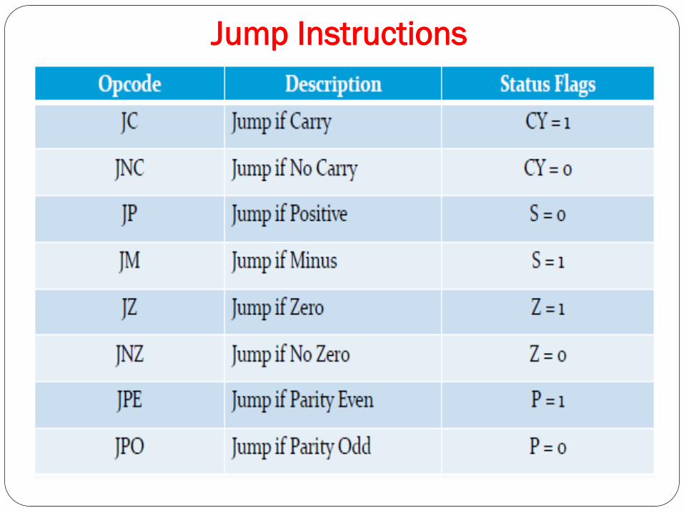
Jump Instructions
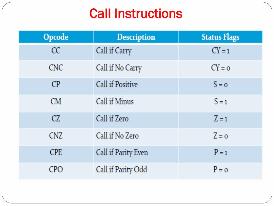
Call Instructions
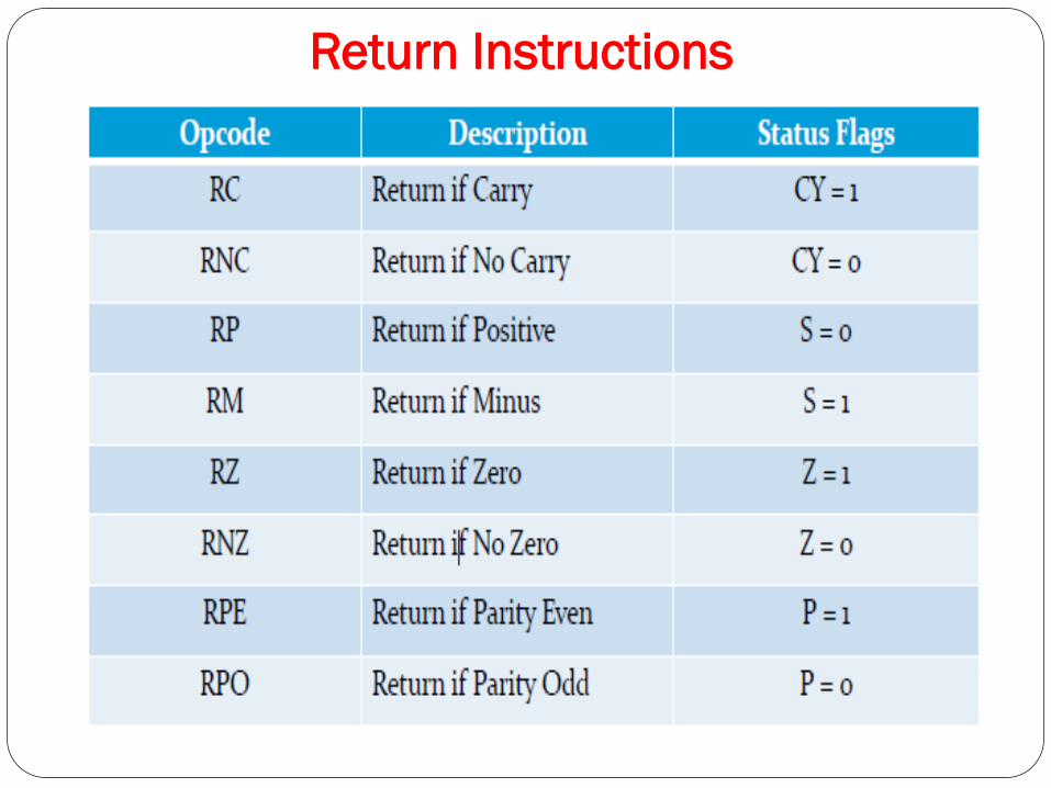
Return Instructions
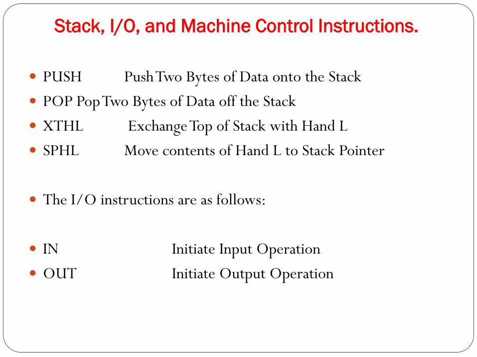
Stack, I/O, and Machine Control Instructions.
PUSH Push Two Bytes of Data onto the Stack
POP Pop Two Bytes of Data off the Stack
XTHL Exchange Top of Stack with Hand L
SPHL Move contents of Hand L to Stack Pointer
The I/O instructions are as follows:
IN Initiate Input Operation
OUT Initiate Output Operation
Stack, I/O, and Machine Control Instructions.
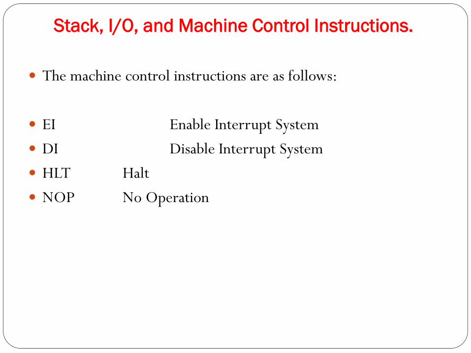
The machine control instructions are as follows:
EI Enable Interrupt System
DI Disable Interrupt System
HLT Halt
NOP No Operation
MODULE 2
TIMING DIAGRAM
ICET34

PROCESSOR AND MECHINE
CYCLE
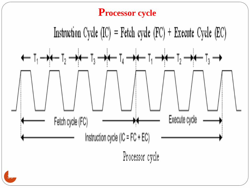
Processor cycle
36
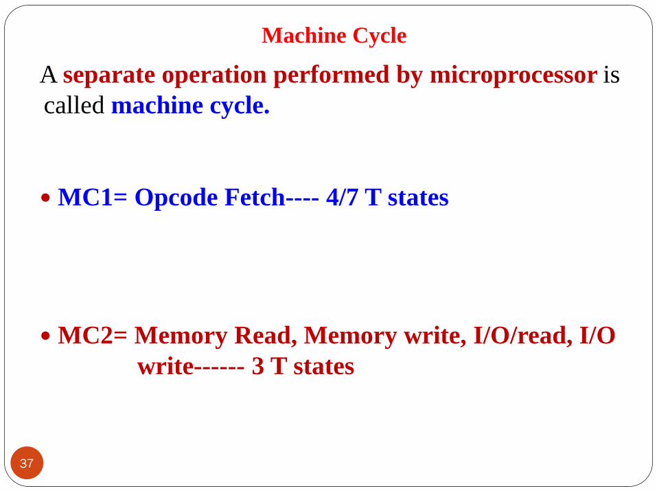
Machine Cycle
A separate operation performed by microprocessor is
called machine cycle.
MC1= Opcode Fetch---- 4/7 T states
MC2= Memory Read, Memory write, I/O/read, I/O
write------ 3 T states
37
INSTUCTION EXECUTION
Instruction Execution
Microprocessor reads the instruction byte by byte and then
executes it.
The instruction execution cycle can be clearly
divided into three different parts
• Fetch Cycle
The fetch cycle takes data required from memory, stores it in
the instruction register.
39
Instruction execution
Decode Cycle
It determines which opcode and addressing mode have been
used, and as such what actions need to be carried out in order
to execute the instruction.
Execute Cycle
The actual actions which occur during the execute cycle of an
instruction.
40
Instruction execution
OPCODE
Opcode is nothing but the machine language instruction which
denotes the microprocessor about what operation should
be performed on the specific data.
OPERAND
The data followed by opcode.
41
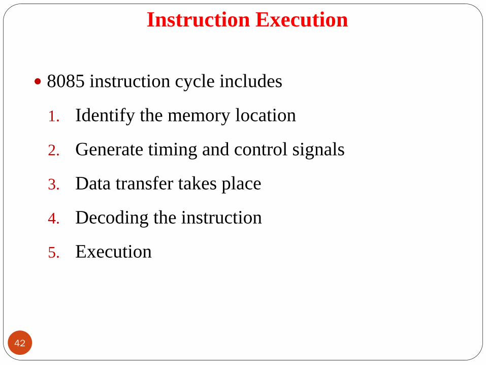
Instruction Execution
8085 instruction cycle includes
1. Identify the memory location
2. Generate timing and control signals
3. Data transfer takes place
4. Decoding the instruction
5. Execution
42
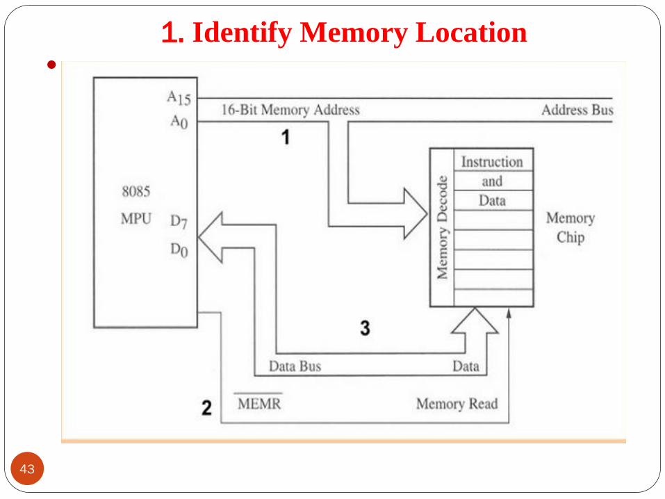
1. Identify Memory Location
43
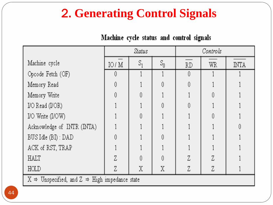
2. Generating Control Signals
44
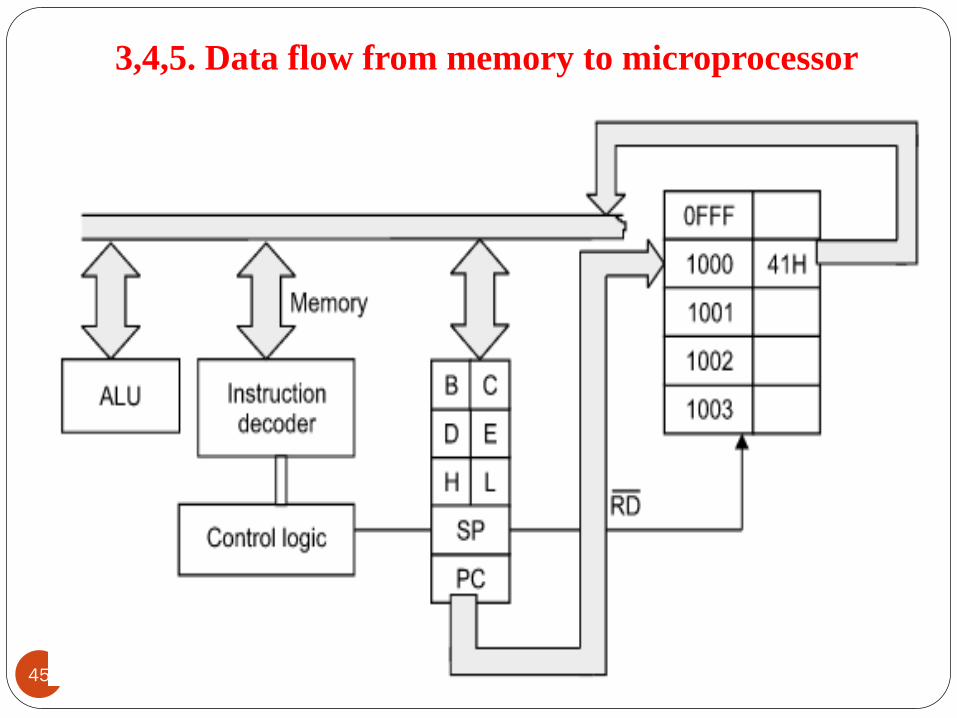
3,4,5. Data flow from memory to microprocessor
45
3,4,5. Data flow from memory to microprocessor
Memory usually starts at address 0000h and could go up to
FFFFh (216 or 64K or 65536 in total).
To access these locations, a 16 bit address is presented to
memory and the byte at that location is either read or written.
The Program Counter is what holds this address when the
micro is executing instructions.
46
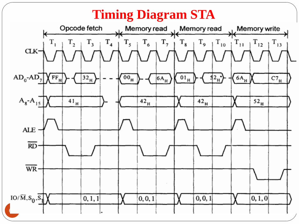
TIMING DIAGRAMS
Timing Diagram examples
Timing diagram is the graphical representation of the initiation of read/write and transfer of data operations under the control of 3-status signals IO / M, S1, and S0.
In 8085 , we have 5 machine cycles
1. Opcode fetch
2. Memory read
3. Memory Write
4. I/O read
5. I/O write
48
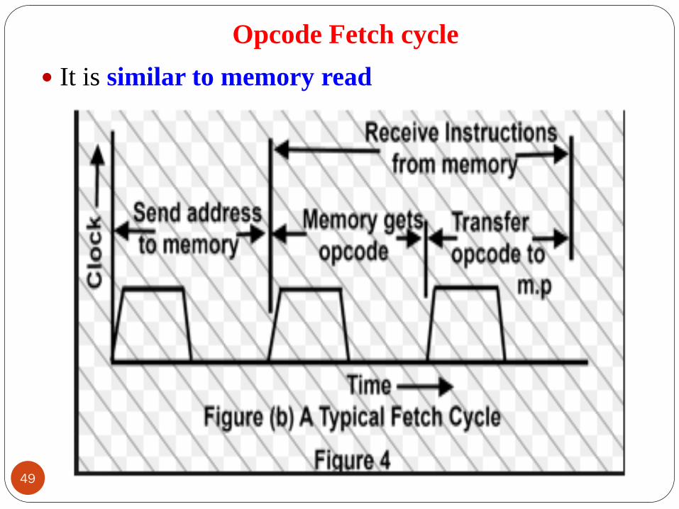
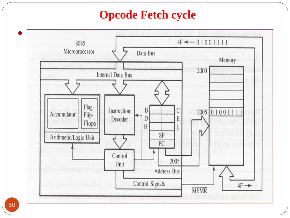
Opcode Fetch cycle
It is similar to memory read
49
Opcode Fetch cycle
50
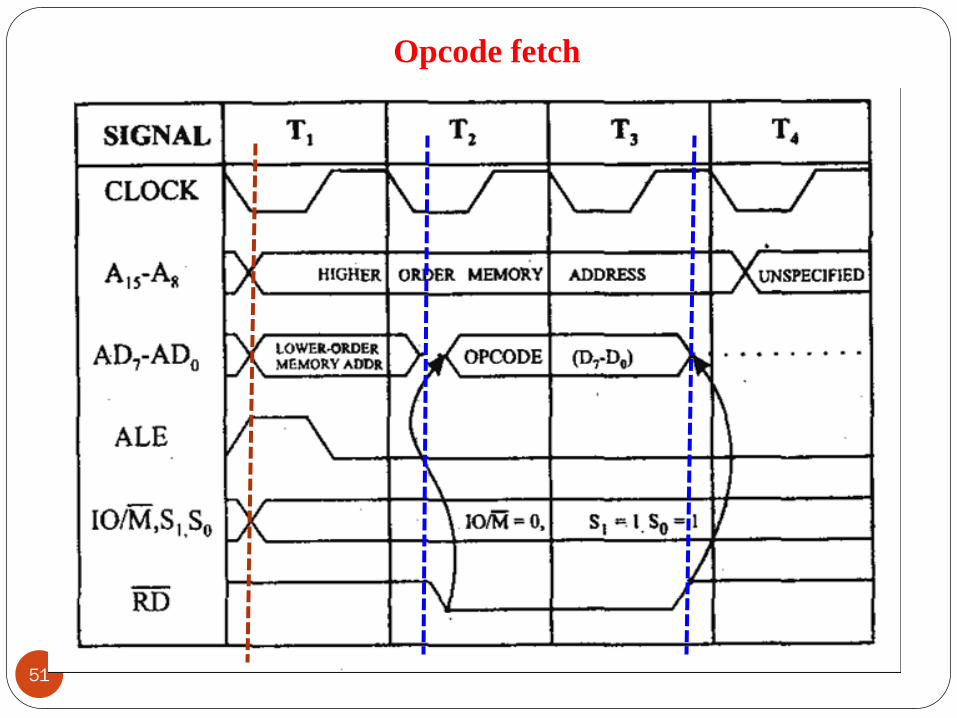
Opcode fetch
51
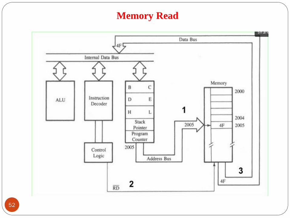
Memory Read
52
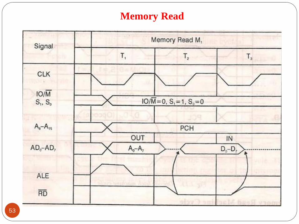
Memory Read
53
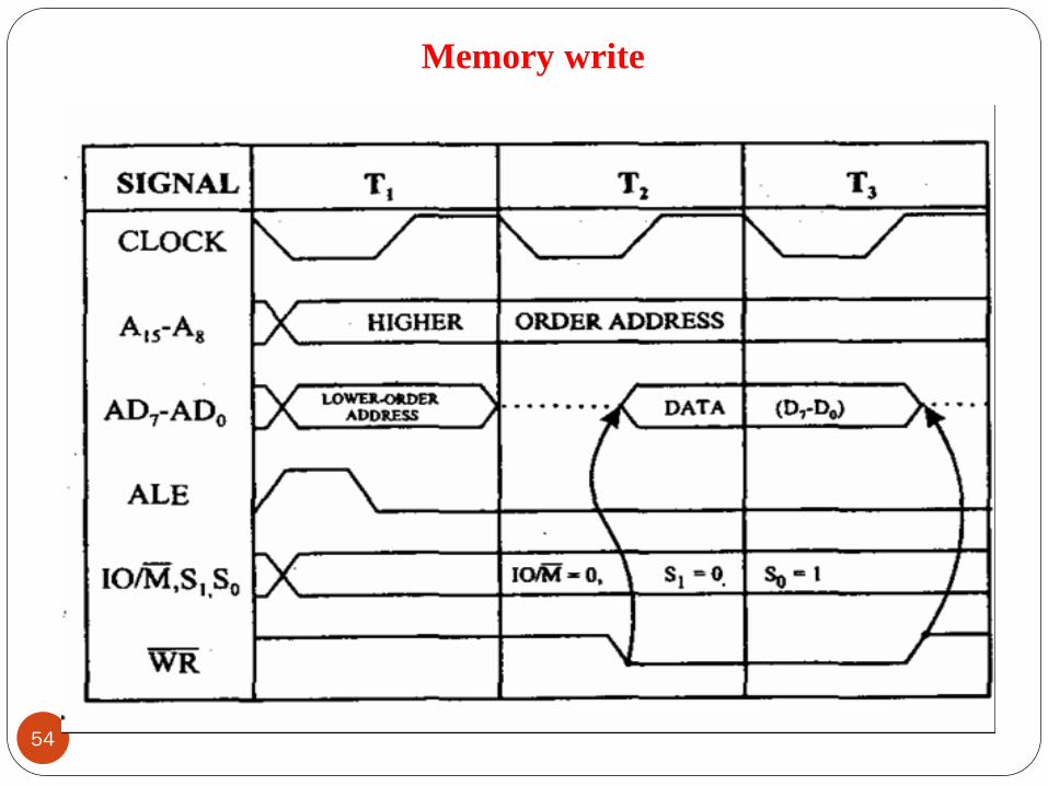
Memory write
54
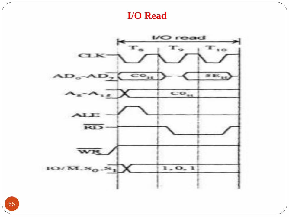
I/O Read
55
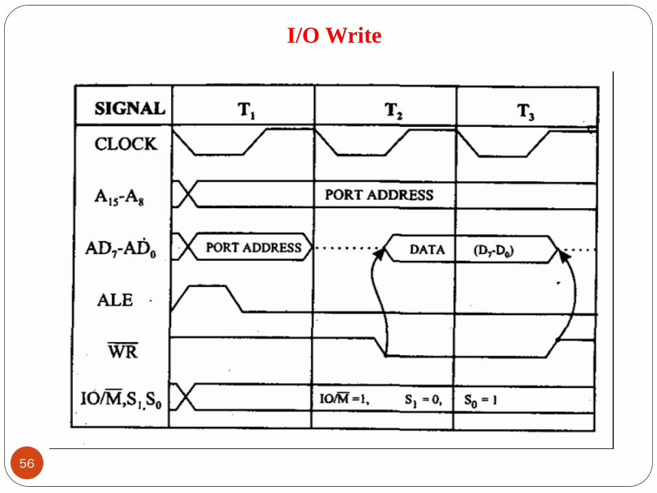
I/O Write
56
TIMING DIAGRAMS
EXAMPLE
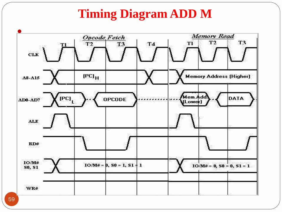
Timing Diagram ADD M
59
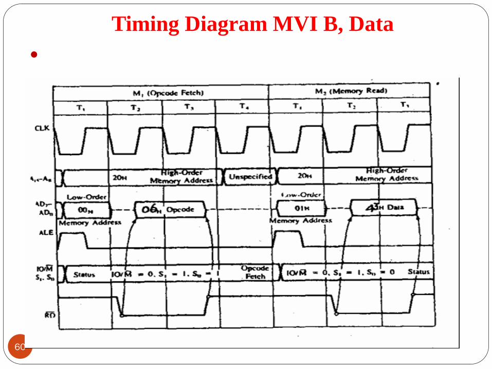
Timing Diagram MVI B, Data
60
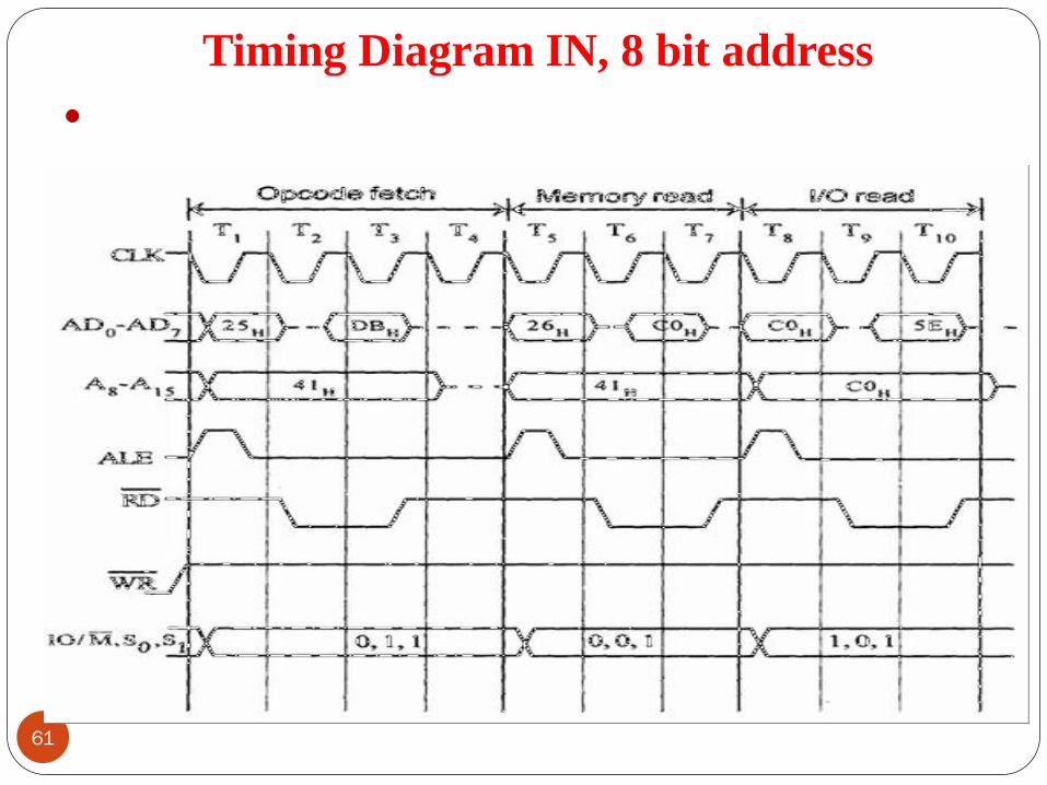
Timing Diagram IN, 8 bit address
61
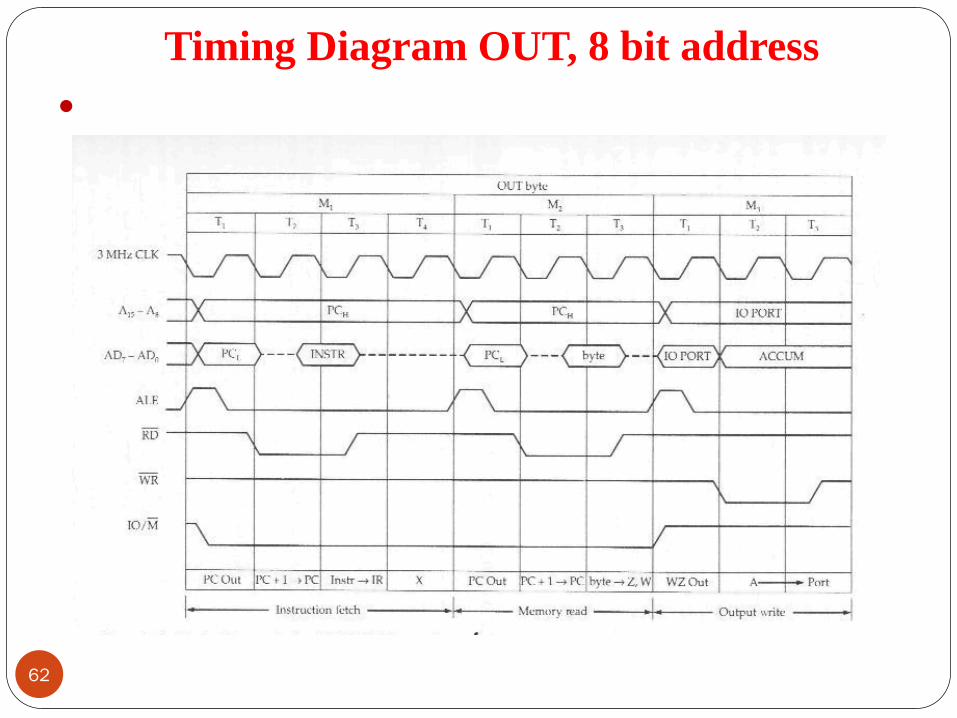
Timing Diagram OUT, 8 bit address
62
Timing Diagram STA
63
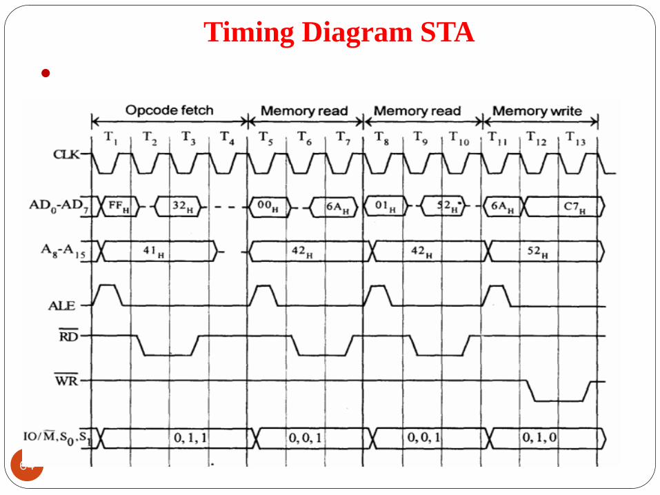
Timing Diagram STA
64
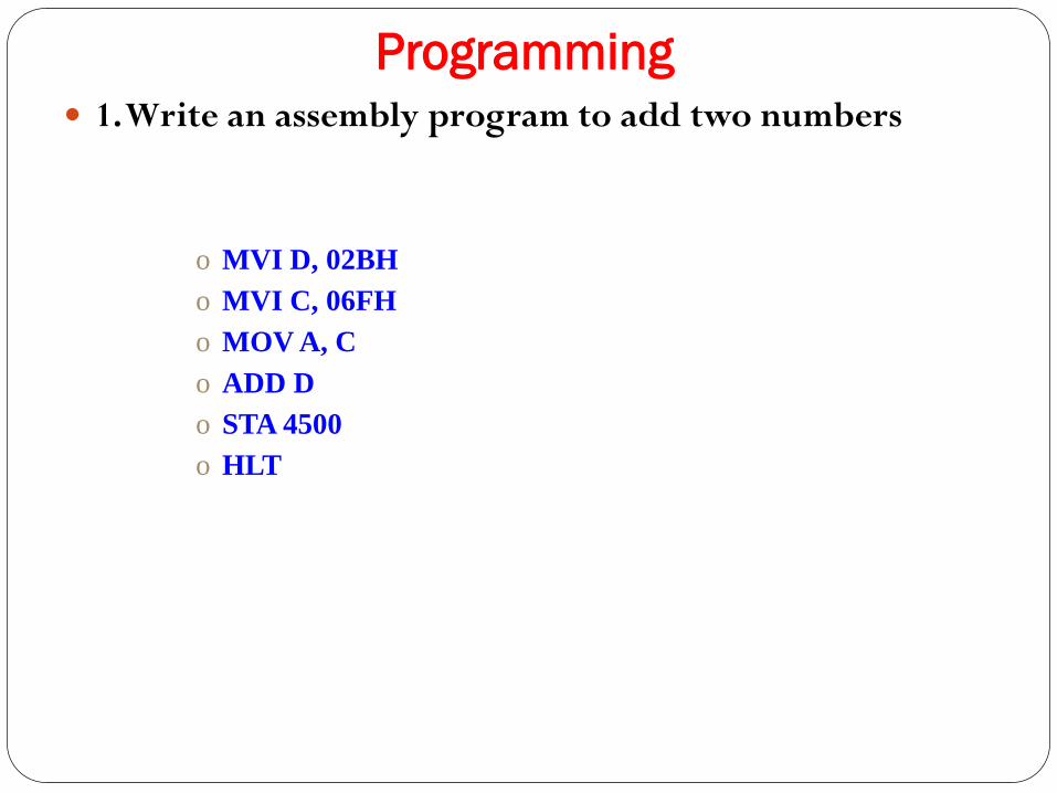
Programming 1. Write an assembly program to add two numbers
o MVI D, 02BH
o MVI C, 06FH
o MOV A, C
o ADD D
o STA 4500
o HLT
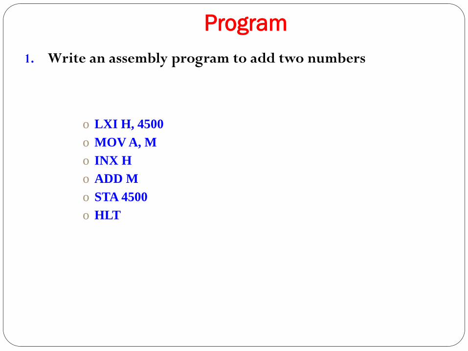
Program
1. Write an assembly program to add two numbers
o LXI H, 4500
o MOV A, M
o INX H
o ADD M
o STA 4500
o HLT
Program
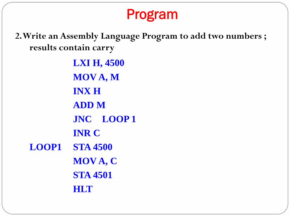
2. Write an Assembly Language Program to add two numbers ;
results contain carry
LXI H, 4500
MOV A, M
INX H
ADD M
JNC LOOP 1
INR C
LOOP1 STA 4500
MOV A, C
STA 4501
HLT
Program
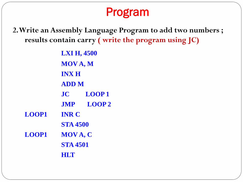
2. Write an Assembly Language Program to add two numbers ;
results contain carry ( write the program using JC)
LXI H, 4500
MOV A, M
INX H
ADD M
JC LOOP 1
JMP LOOP 2
LOOP1 INR C
STA 4500
LOOP1 MOV A, C
STA 4501
HLT
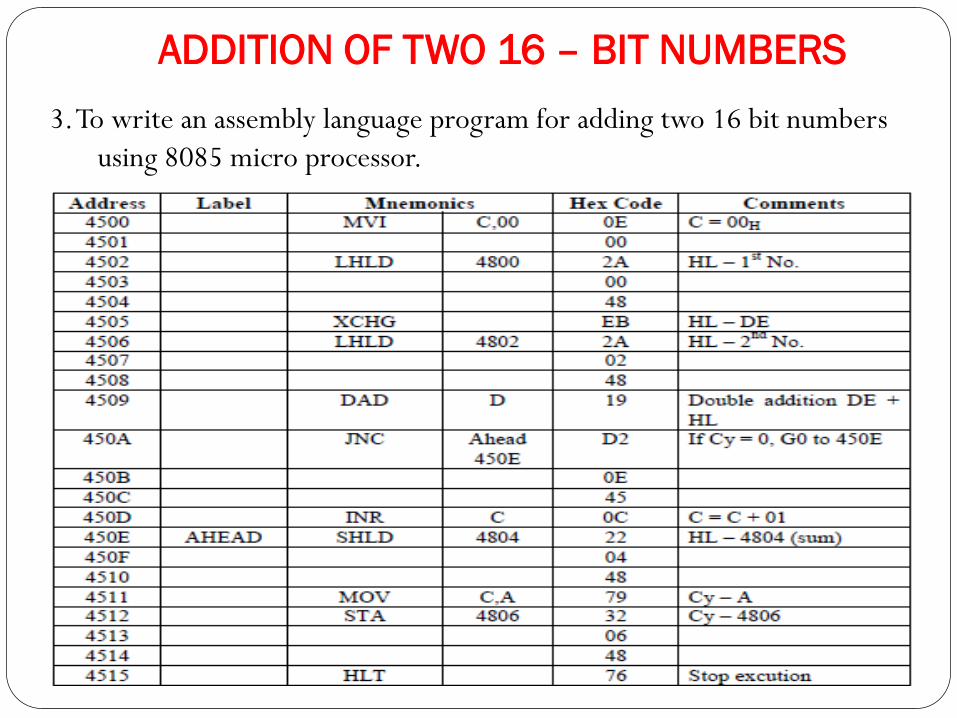
ADDITION OF TWO 16 – BIT NUMBERS
3. To write an assembly language program for adding two 16 bit numbers
using 8085 micro processor.
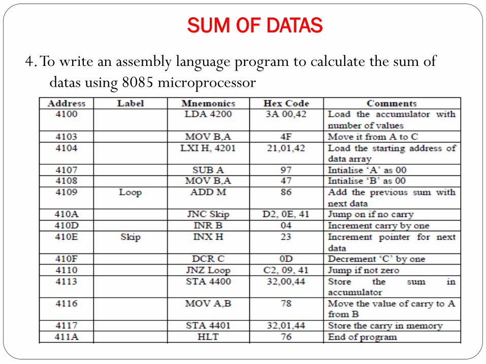
SUM OF DATAS
4. To write an assembly language program to calculate the sum of
datas using 8085 microprocessor
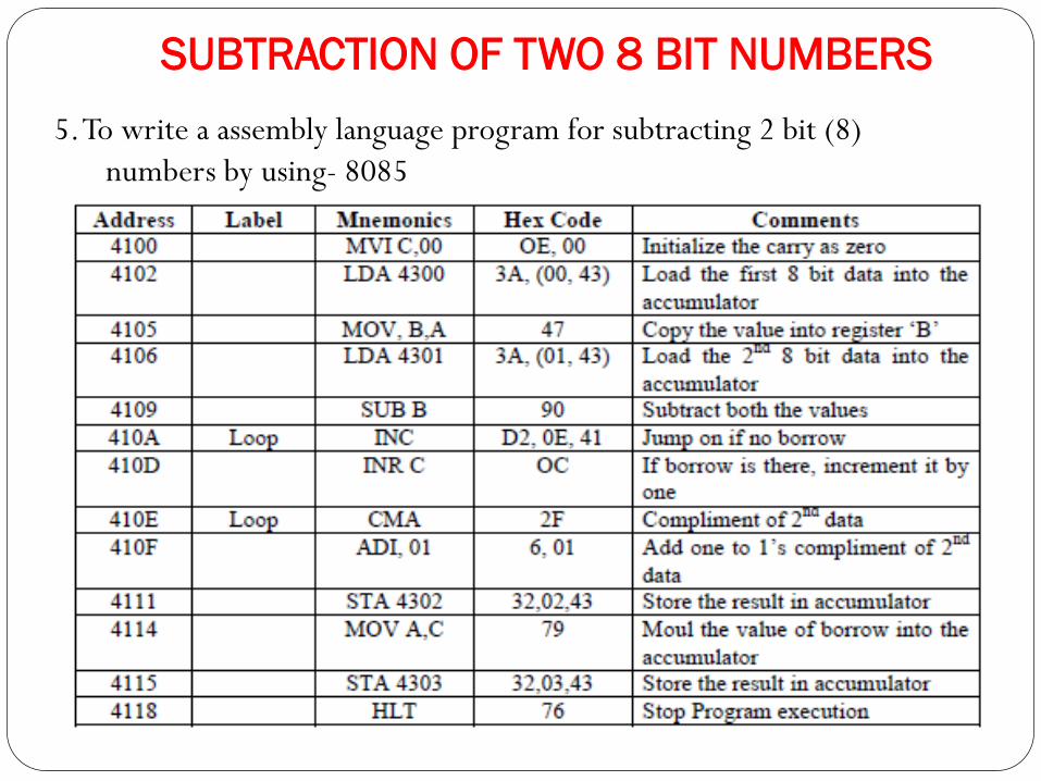
SUBTRACTION OF TWO 8 BIT NUMBERS
5. To write a assembly language program for subtracting 2 bit (8)
numbers by using- 8085
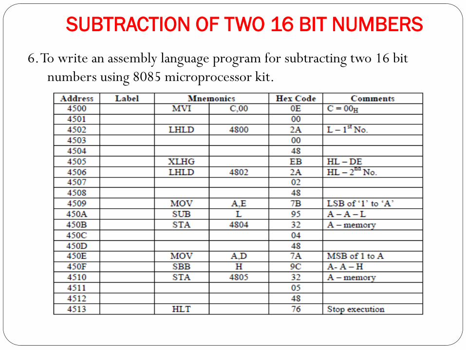
SUBTRACTION OF TWO 16 BIT NUMBERS
6. To write an assembly language program for subtracting two 16 bit
numbers using 8085 microprocessor kit.
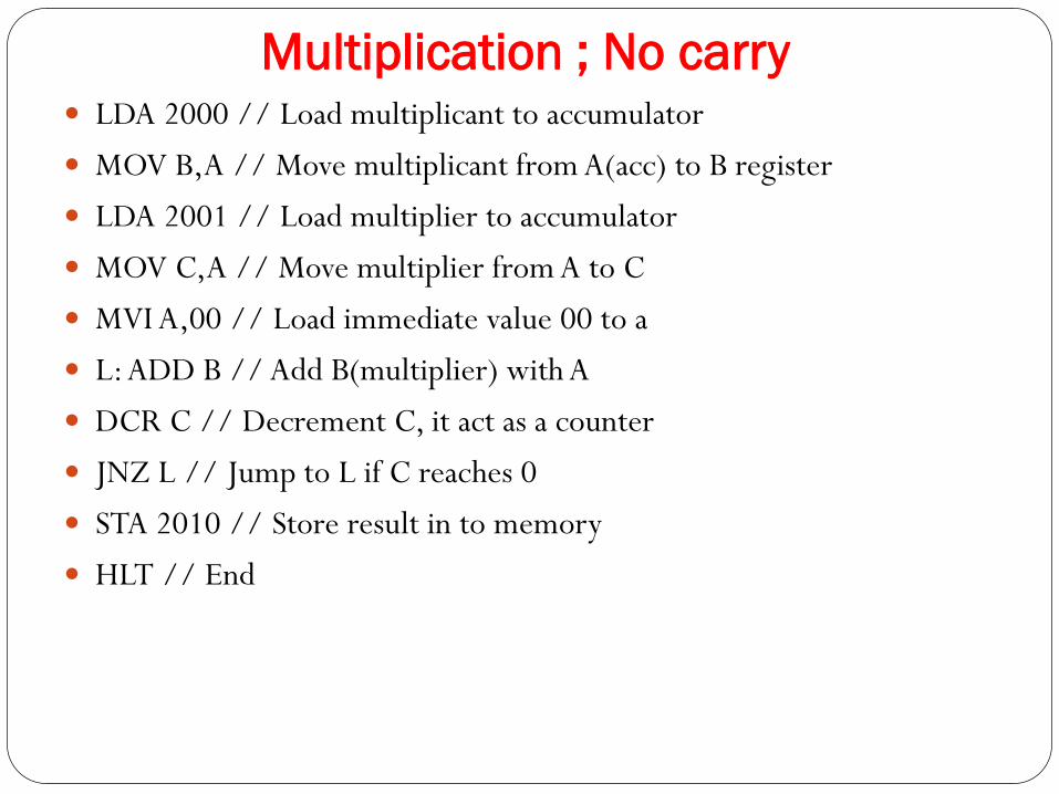
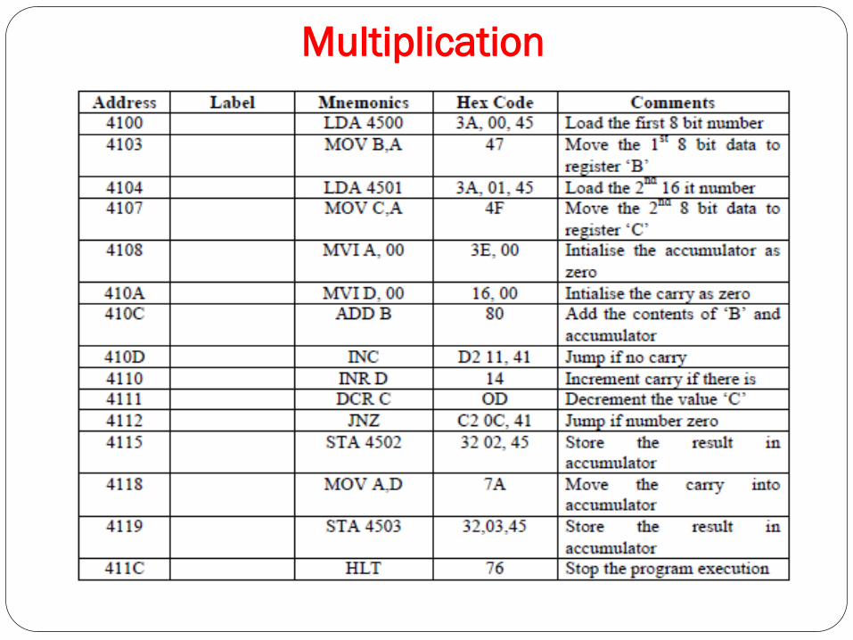
Multiplication ; No carry LDA 2000 // Load multiplicant to accumulator
MOV B,A // Move multiplicant from A(acc) to B register
LDA 2001 // Load multiplier to accumulator
MOV C,A // Move multiplier from A to C
MVI A,00 // Load immediate value 00 to a
L: ADD B // Add B(multiplier) with A
DCR C // Decrement C, it act as a counter
JNZ L // Jump to L if C reaches 0
STA 2010 // Store result in to memory
HLT // End
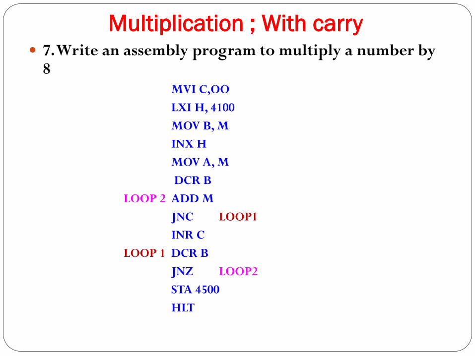
Multiplication ; With carry 7. Write an assembly program to multiply a number by
8MVI C,OO
LXI H, 4100
MOV B, M
INX H
MOV A, M
DCR B
LOOP 2 ADD M
JNC LOOP1
INR C
LOOP 1 DCR B
JNZ LOOP2
STA 4500
HLT
Multiplication
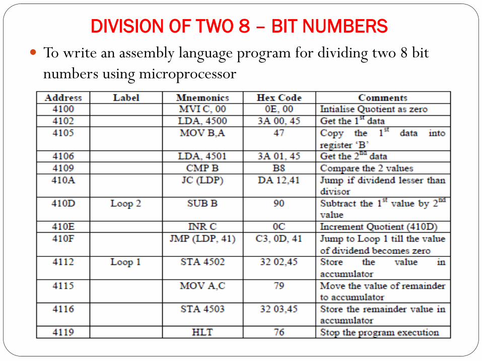
DIVISION OF TWO 8 – BIT NUMBERS
To write an assembly language program for dividing two 8 bit
numbers using microprocessor
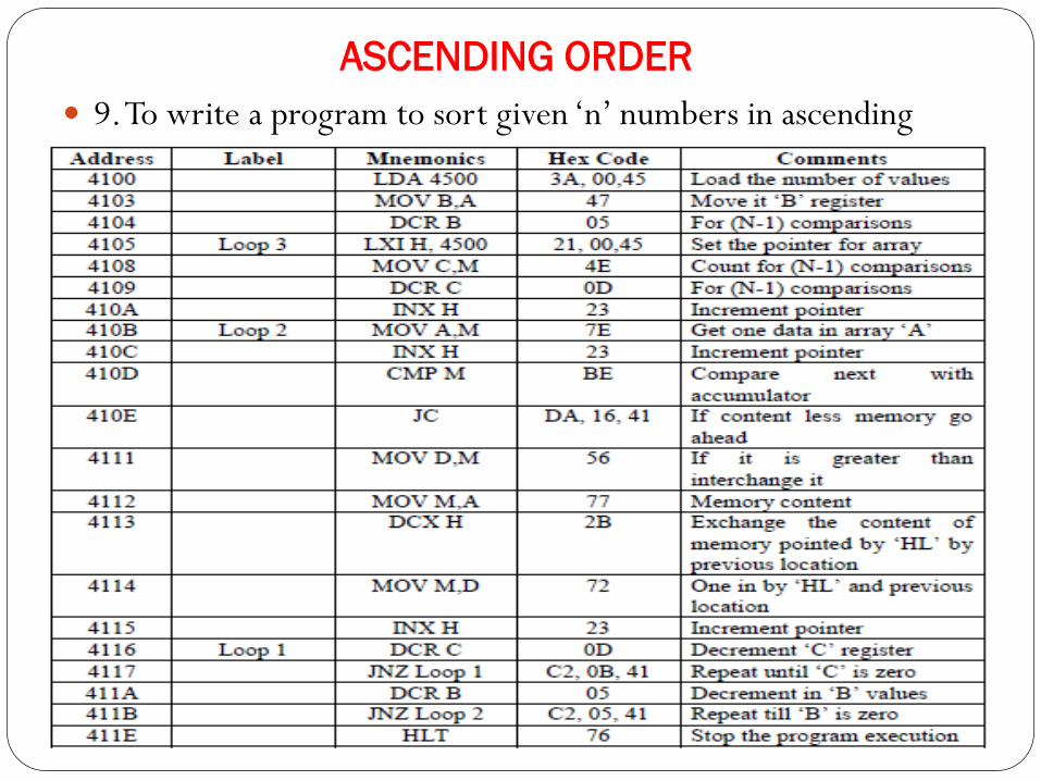
ASCENDING ORDER
9. To write a program to sort given ‘n’ numbers in ascending
order
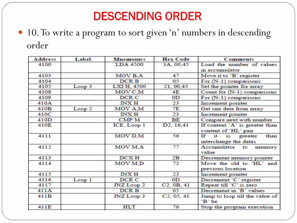
DESCENDING ORDER
10. To write a program to sort given ‘n’ numbers in descending
order
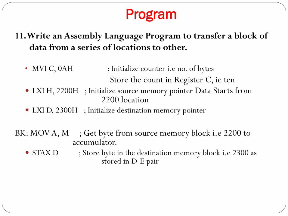
Program
11. Write an Assembly Language Program to transfer a block of
data from a series of locations to other.
• MVI C, 0AH ; Initialize counter i.e no. of bytes
Store the count in Register C, ie ten LXI H, 2200H ; Initialize source memory pointer Data Starts from
2200 location LXI D, 2300H ; Initialize destination memory pointer
BK: MOV A, M ; Get byte from source memory block i.e 2200 to accumulator.
STAX D ; Store byte in the destination memory block i.e 2300 as stored in D-E pair
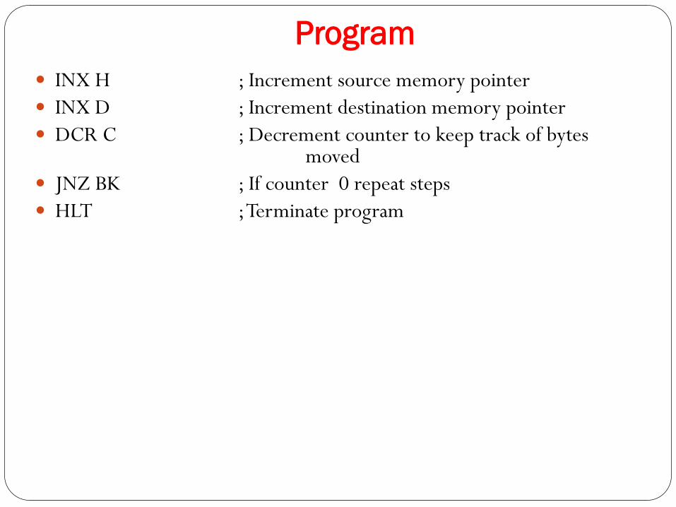
Program
INX H ; Increment source memory pointer
INX D ; Increment destination memory pointer
DCR C ; Decrement counter to keep track of bytes moved
JNZ BK ; If counter 0 repeat steps
HLT ; Terminate program
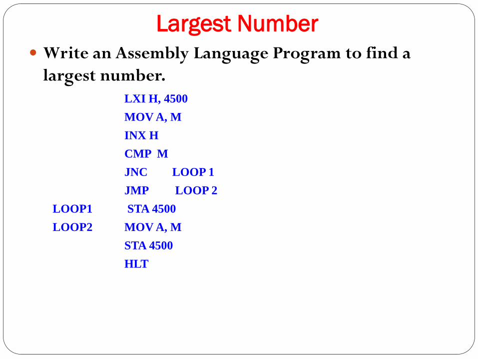
Largest Number
Write an Assembly Language Program to find a
largest number.
LXI H, 4500
MOV A, M
INX H
CMP M
JNC LOOP 1
JMP LOOP 2
LOOP1 STA 4500
LOOP2 MOV A, M
STA 4500
HLT
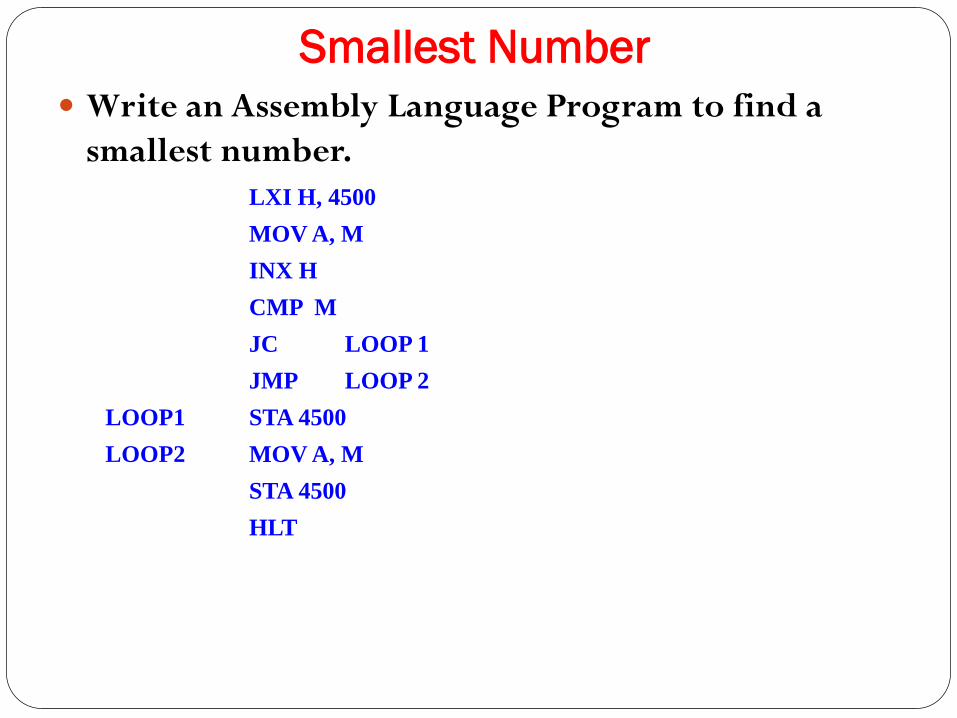
Smallest Number
Write an Assembly Language Program to find a
smallest number.
LXI H, 4500
MOV A, M
INX H
CMP M
JC LOOP 1
JMP LOOP 2
LOOP1 STA 4500
LOOP2 MOV A, M
STA 4500
HLT
STACK AND SUBROUTINE
DEEPAK.P83
9/8/14
STACK
The stack is an area of memory identified by the
programmer for temporary storage of information.
The stack is a LIFO structure.
The stack normally grows backwards into memory.
Programmer can defines the bottom of (SP) the stack
and the stack grows up into reducing address range.
STACK
Stack is defined by setting the SP (Stack Pointer)
register.
LXI SP, FFFFH ,This sets SP to location FFFFH (end of memory
for 8085).
STACK
Save information by PUSHing onto STACK
Retrieved from STACK by POPing it off.
PUSH and POP work with register pairs only.
Example “PUSH B”
– Decrement SP, Copy B to (SP-1)
– Decrement SP, Copy C to (SP-1)
Example “POP B”
– Copy (SP+1) to C, Increment SP
– Copy (SP+1) to B, Increment SP
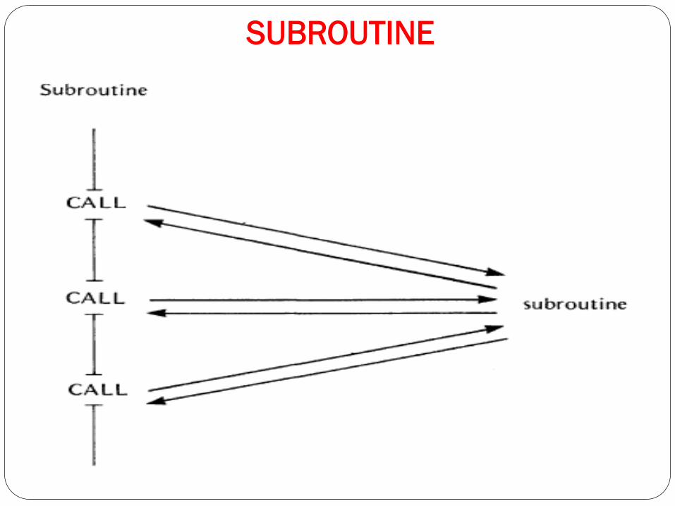
SUBROUTINE A subroutine is a group of instructions that is used
repeatedly in different places of the program.
It can be grouped into a subroutine and call from the
different locations.
The CALL instruction is used to redirect program execution
to the subroutine.
The RET instruction is used to return the execution to the
calling routine.
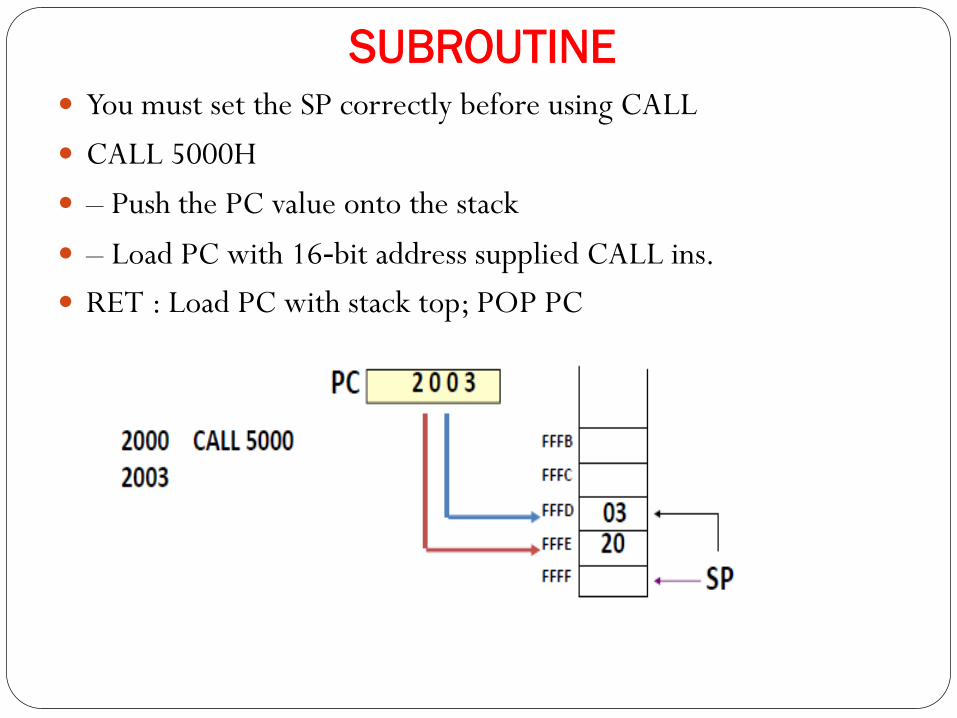
SUBROUTINE You must set the SP correctly before using CALL
CALL 5000H
– Push the PC value onto the stack
– Load PC with 16‐bit address supplied CALL ins.
RET : Load PC with stack top; POP PC
SUBROUTINE
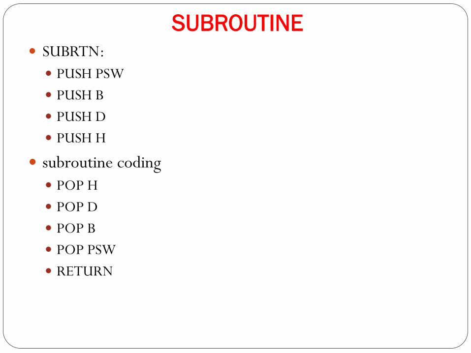
SUBROUTINE SUBRTN:
PUSH PSW
PUSH B
PUSH D
PUSH H
subroutine coding
POP H
POP D
POP B
POP PSW
RETURN
MODULE 3
INTERFACING
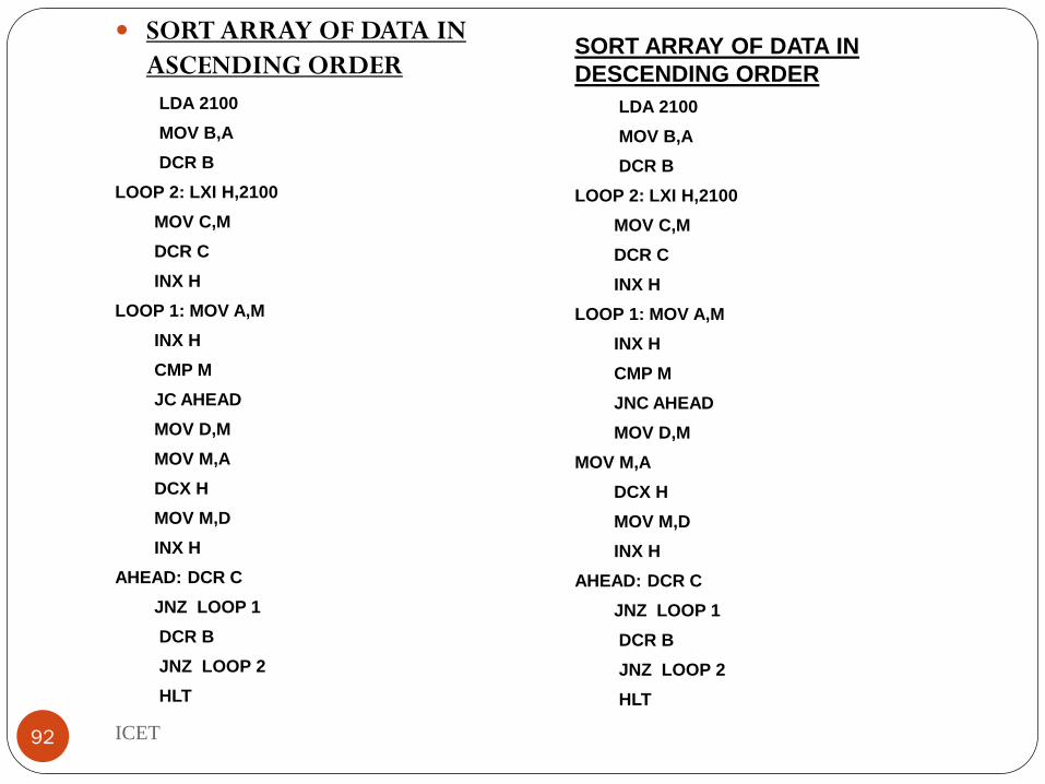
SORT ARRAY OF DATA IN
ASCENDING ORDER
LDA 2100
MOV B,A
DCR B
LOOP 2: LXI H,2100
MOV C,M
DCR C
INX H
LOOP 1: MOV A,M
INX H
CMP M
JC AHEAD
MOV D,M
MOV M,A
DCX H
MOV M,D
INX H
AHEAD: DCR C
JNZ LOOP 1
DCR B
JNZ LOOP 2
HLT
SORT ARRAY OF DATA IN
DESCENDING ORDER
LDA 2100
MOV B,A
DCR B
LOOP 2: LXI H,2100
MOV C,M
DCR C
INX H
LOOP 1: MOV A,M
INX H
CMP M
JNC AHEAD
MOV D,M
MOV M,A
DCX H
MOV M,D
INX H
AHEAD: DCR C
JNZ LOOP 1
DCR B
JNZ LOOP 2
HLT
92 ICET
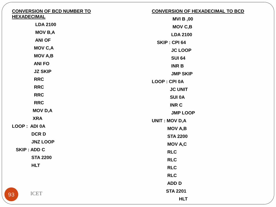
CONVERSION OF BCD NUMBER TO
HEXADECIMAL
LDA 2100
MOV B,A
ANI OF
MOV C,A
MOV A,B
ANI FO
JZ SKIP
RRC
RRC
RRC
RRC
MOV D,A
XRA
LOOP : ADI 0A
DCR D
JNZ LOOP
SKIP : ADD C
STA 2200
HLT
CONVERSION OF HEXADECIMAL TO BCD
MVI B ,00
MOV C,B
LDA 2100
SKIP : CPI 64
JC LOOP
SUI 64
INR B
JMP SKIP
LOOP : CPI 0A
JC UNIT
SUI 0A
INR C
JMP LOOP
UNIT : MOV D,A
MOV A,B
STA 2200
MOV A,C
RLC
RLC
RLC
RLC
ADD D
STA 2201
HLT93 ICET
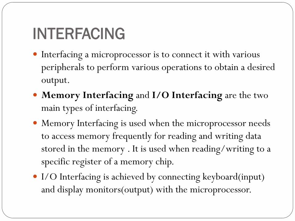
INTERFACING
Interfacing a microprocessor is to connect it with various
peripherals to perform various operations to obtain a desired
output.
Memory Interfacing and I/O Interfacing are the two
main types of interfacing.
Memory Interfacing is used when the microprocessor needs
to access memory frequently for reading and writing data
stored in the memory . It is used when reading/writing to a
specific register of a memory chip.
I/O Interfacing is achieved by connecting keyboard(input)
and display monitors(output) with the microprocessor.
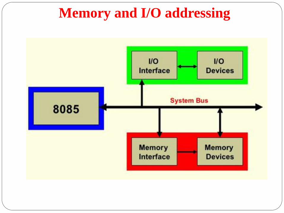
Memory and I/O addressing
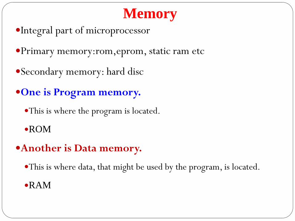
MemoryIntegral part of microprocessor
Primary memory:rom,eprom, static ram etc
Secondary memory: hard disc
One is Program memory.
This is where the program is located.
ROM
Another is Data memory.
This is where data, that might be used by the program, is located.
RAM
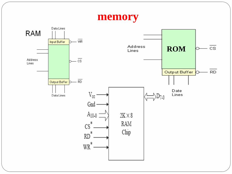
memory
ROM
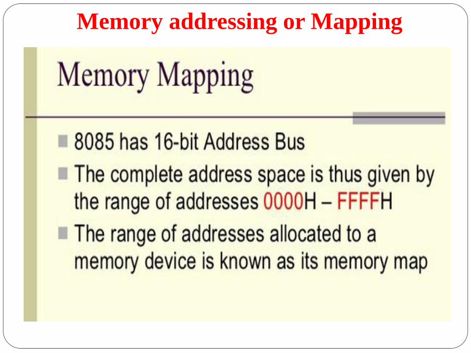
Memory addressing or Mapping
Memory addressing or Mapping
Memory addressing or Mapping
Memory interfacing
Memory interfacing 64KB
Interface a 8085 system in which full memory space
utilized for EPROM memory
Memory interfacing 64KB
In this system the entire 16 address lines of the processor are
connected to address input pins of memory IC.
The chip select (CS) pin of EPROM is permanently tied to
logic low (i.e., tied to ground).
Since the processor is connected to EPROM, the active low
RD pin is connected to active low output enable pin of
EPROM.
The range of address for EPROM is 0000H to FFFFH.
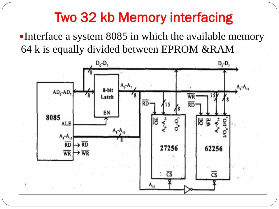
Two 32 kb Memory interfacing
Interface a system 8085 in which the available memory
64 k is equally divided between EPROM &RAM
Two 32 kb Memory interfacing
Implement 32kb memory capacity of EPROM using single
IC 27256.
32kb RAM capacity is implemented using single IC 62256.
The 32kb memory requires 15 address lines and so the
address lines A0 - A14 of the processor are connected to 15
address pins of both EPROM and RAM.
Two 32 kb Memory interfacing
The 32kb memory requires 15 address lines and so the
address lines A0 - A14 of the processor are connected to 15
address pins of both EPROM and RAM.
The unused address line A15 is used as to chip select. If
A15 is 1, it select RAM and If A15 is 0, it select EPROM.
The memory used is both Ram and EPROM, so the low RD
and WR pins of processor are connected to low WE and OE
pins of memory respectively.
The address range of EPROM will be 0000H to 7FFFH and
that of RAM will be 7FFFH to FFFFH.
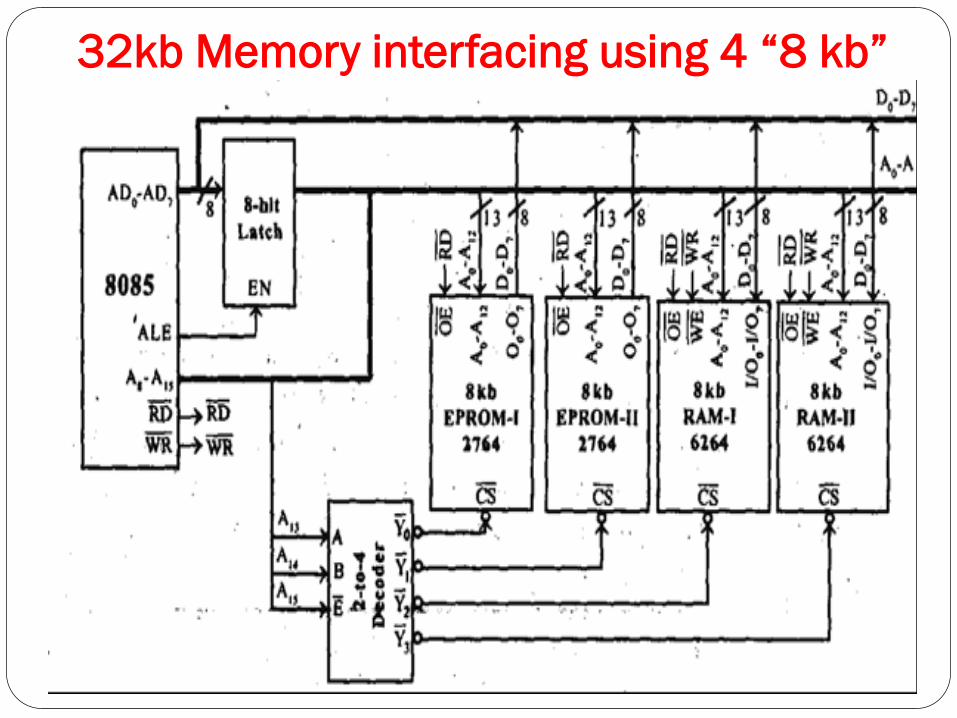
32kb Memory interfacing using 4 “8 kb”
32kb Memory interfacing using 4 “8 kb”
The total memory capacity is 32Kb. So, let two number of
8kb n memory be EPROM and the remaining two numbers
be RAM.
Each 8kb memory requires 13 address lines and so the
address lines A0- A12 of the processor are connected to 13
address pins of all the memory.
The address lines and A13 - A14 can be decoded using a 2-
to-4 decoder to generate four chip select signals.
These four chip select signals can be used to select one of
the four memory IC at any one time.
The address line A15 is used as enable for decoder.
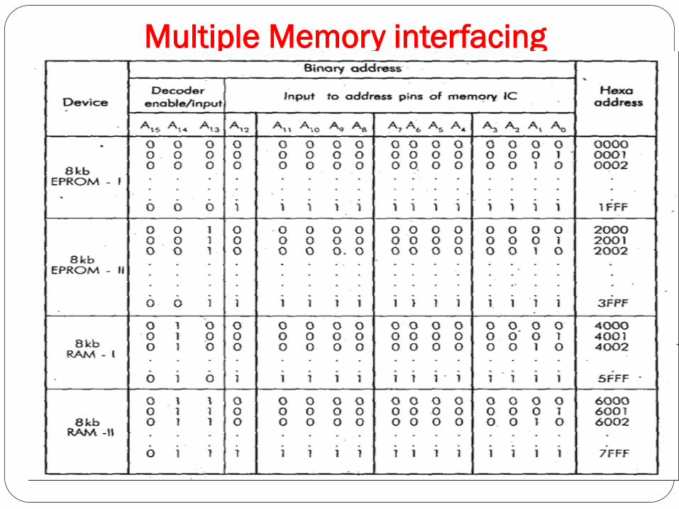
Multiple Memory interfacing
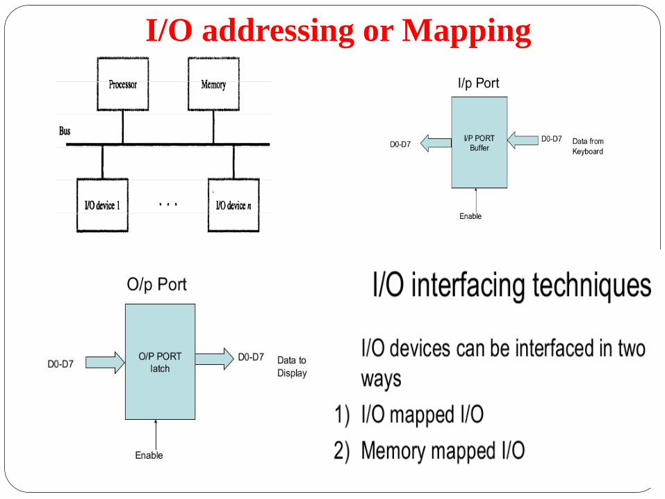
I/O addressing or Mapping
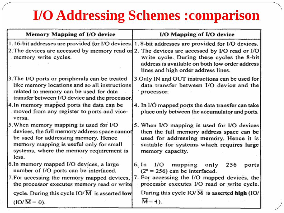
I/O Addressing Schemes :comparison
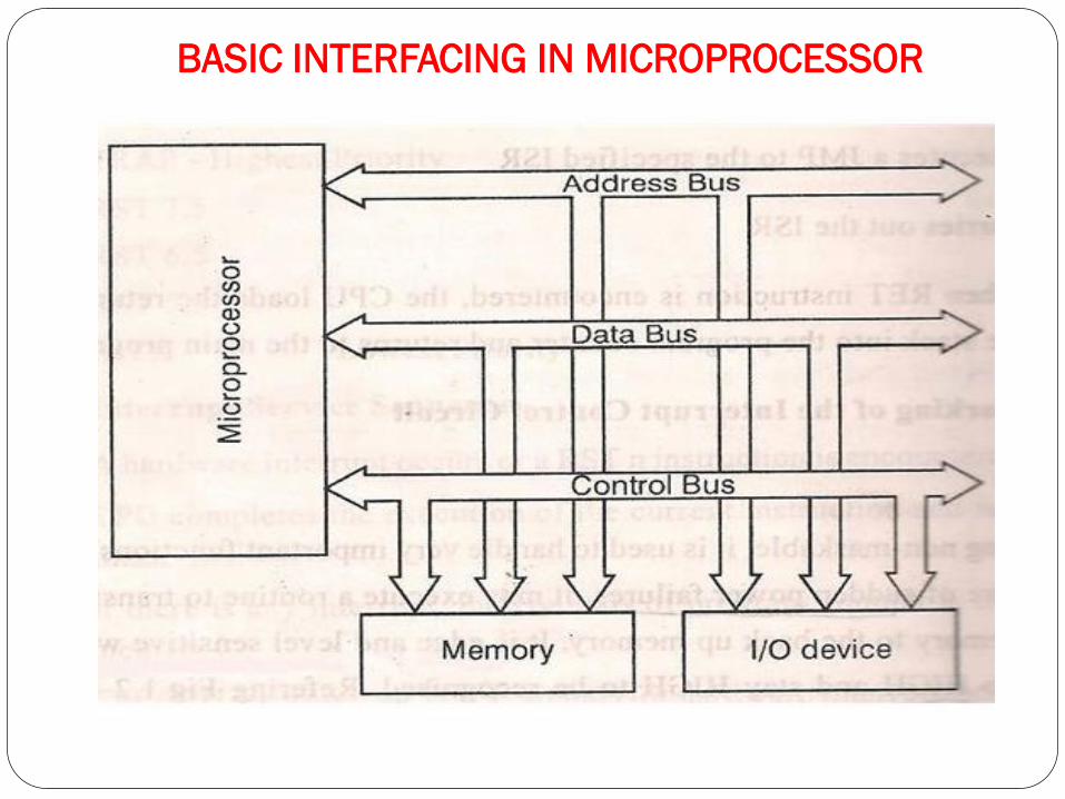
BASIC INTERFACING IN MICROPROCESSOR
BASIC INTERFACING IN MICROPROCESSOR
• In memory interfacing, 8 bit data line, 16 bit
address line , control signals are connected to
corresponding lines of memory IC.
• In I/O device interfacing, 8 bit data line, only 8
bit address line , control signals are connected to
corresponding lines of I/O devices.
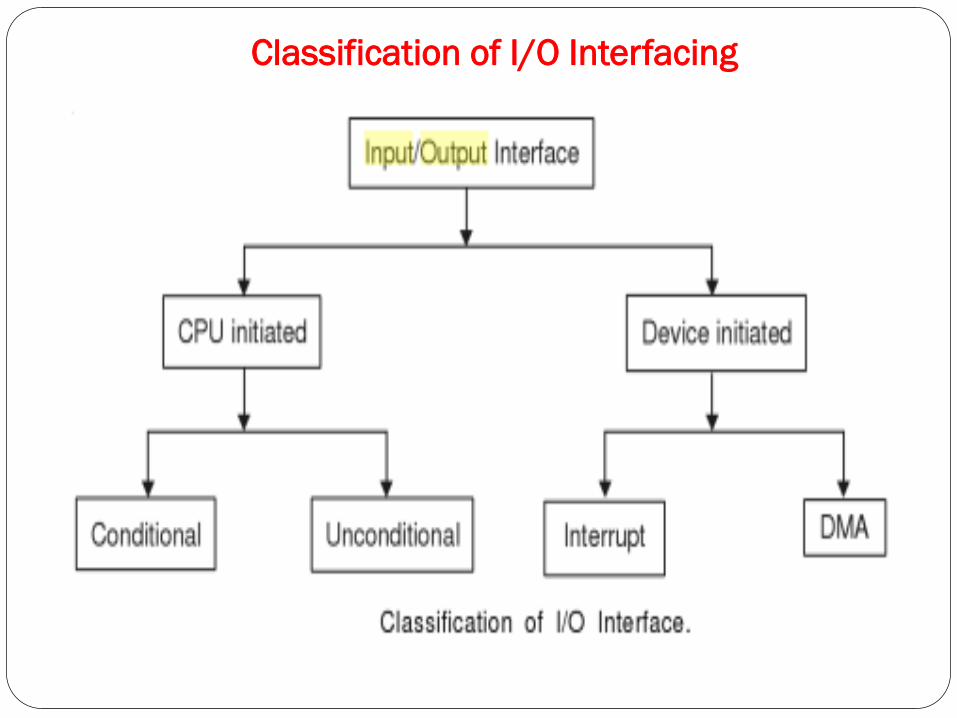
Classification of I/O Interfacing
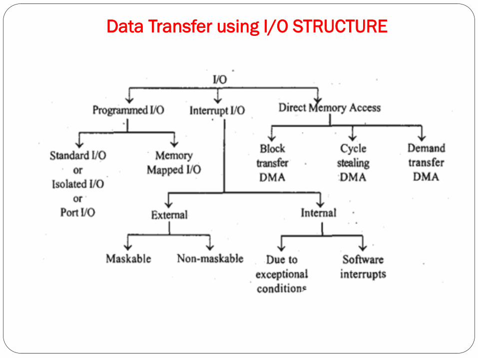
Data Transfer using I/O STRUCTURE
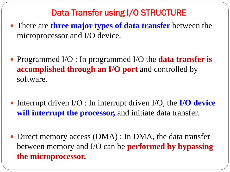
Data Transfer using I/O STRUCTURE
There are three major types of data transfer between the
microprocessor and I/O device.
Programmed I/O : In programmed I/O the data transfer is
accomplished through an I/O port and controlled by
software.
Interrupt driven I/O : In interrupt driven I/O, the I/O device
will interrupt the processor, and initiate data transfer.
Direct memory access (DMA) : In DMA, the data transfer
between memory and I/O can be performed by bypassing
the microprocessor.
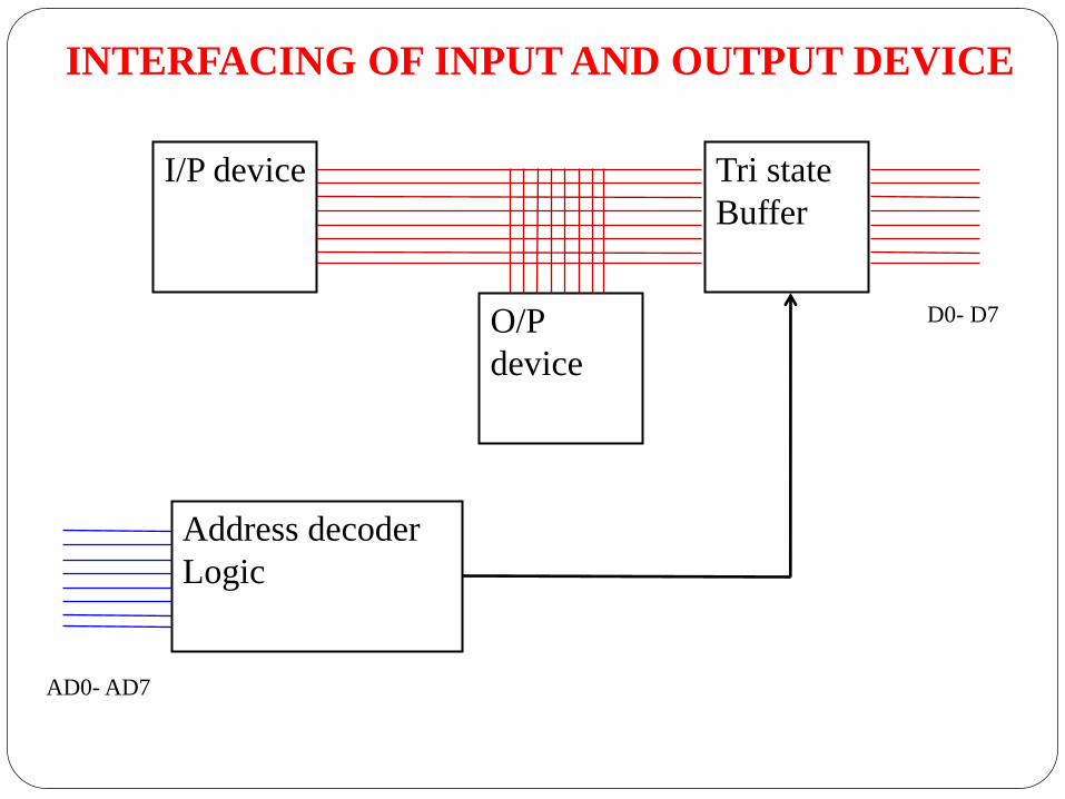
INTERFACING OF INPUT AND OUTPUT DEVICE
I/P device
O/P
device
Tri state
Buffer
Address decoder
Logic
AD0- AD7
D0- D7
INTERFACING OF INPUT AND OUTPUT DEVICE
I/O mapped or programmed interfacing scheme is
commonly used.The data lines are connected to the I/O
devices through Tri-state buffer.Tri- State buffer is
enabled from address decoder logic.
The address decoder logic makes an enable signal
according to the address data coming from
microprocessor.
These address is the address of a ports.
IN and OUT instruction is used for data transfer
Eg. IN ,Port address; IN 02
OUT, Port address; OUT 03
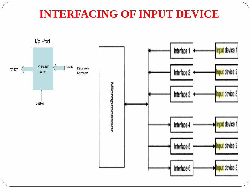
INTERFACING OF INPUT DEVICE

INTERFACING OF INPUT DEVICE
I/P device
O/P
device
Tri state
Buffer
AD0- AD7 D0- D7
I/O/ M
RD Active High
1
11
Not Using
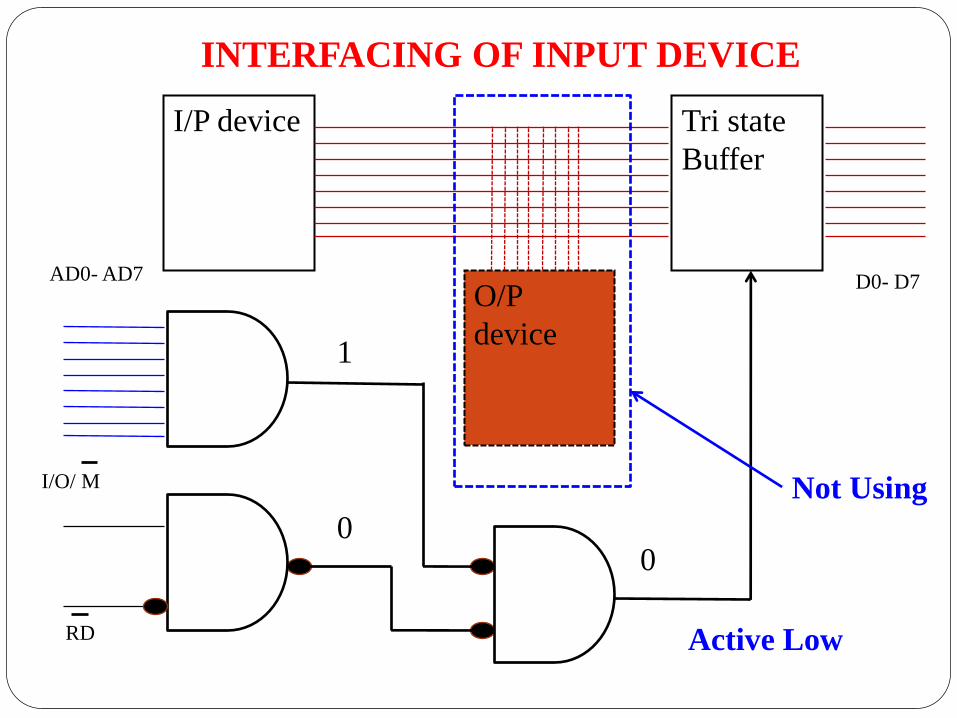
INTERFACING OF INPUT DEVICE
1
00
I/P device
O/P
device
Tri state
Buffer
AD0- AD7 D0- D7
I/O/ M
RD Active Low
Not Using
INTERFACING OF INPUT DEVICE
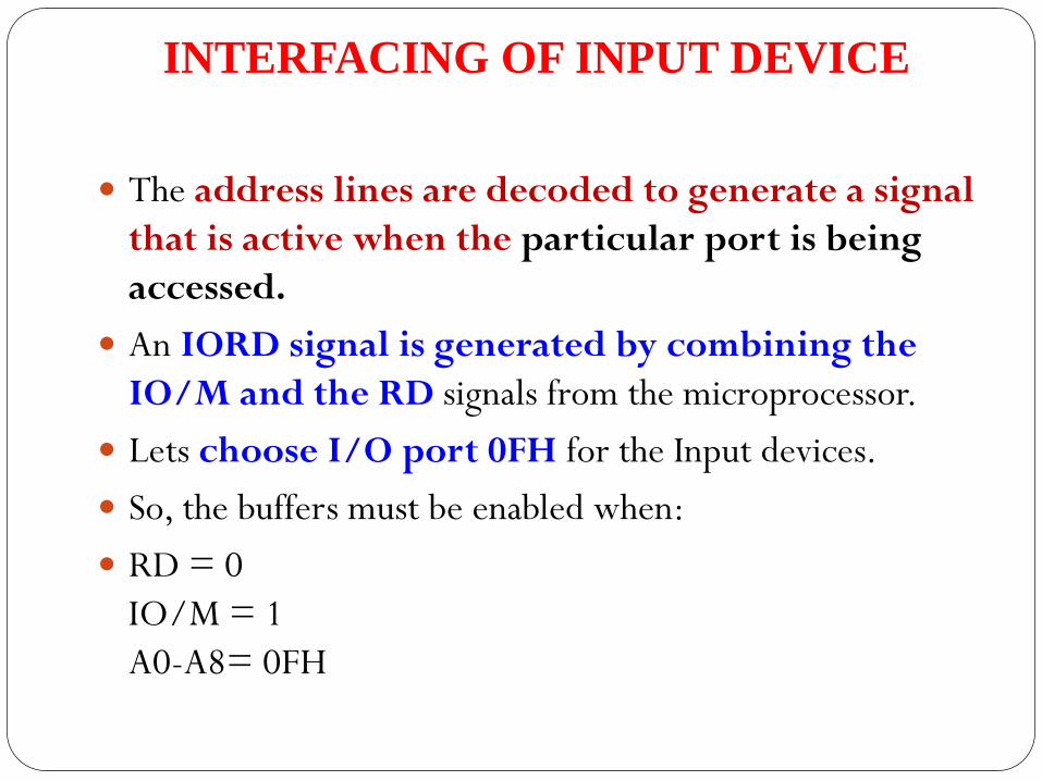
The address lines are decoded to generate a signal
that is active when the particular port is being
accessed.
An IORD signal is generated by combining the
IO/M and the RD signals from the microprocessor.
Lets choose I/O port 0FH for the Input devices.
So, the buffers must be enabled when:
RD = 0
IO/M = 1
A0-A8= 0FH
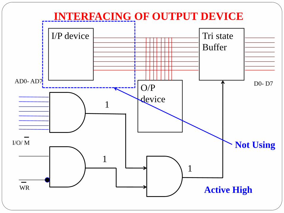
INTERFACING OF OUTPUT DEVICE
I/P device
O/P
device
Tri state
Buffer
AD0- AD7 D0- D7
I/O/ M
WR Active High
1
11
Not Using
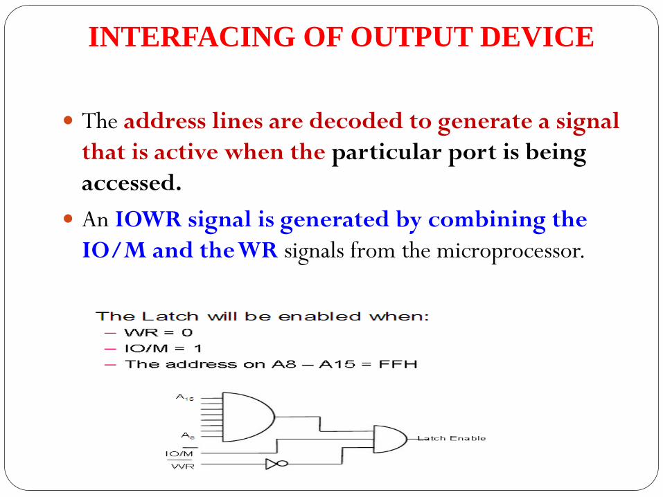
INTERFACING OF OUTPUT DEVICE
The address lines are decoded to generate a signal
that is active when the particular port is being
accessed.
An IOWR signal is generated by combining the
IO/M and the WR signals from the microprocessor.
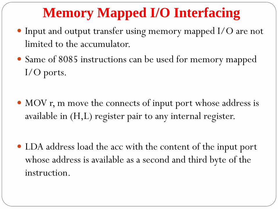
Memory Mapped I/O Interfacing
Input and output transfer using memory mapped I/O are not
limited to the accumulator.
Same of 8085 instructions can be used for memory mapped
I/O ports.
MOV r, m move the connects of input port whose address is
available in (H,L) register pair to any internal register.
LDA address load the acc with the content of the input port
whose address is available as a second and third byte of the
instruction.
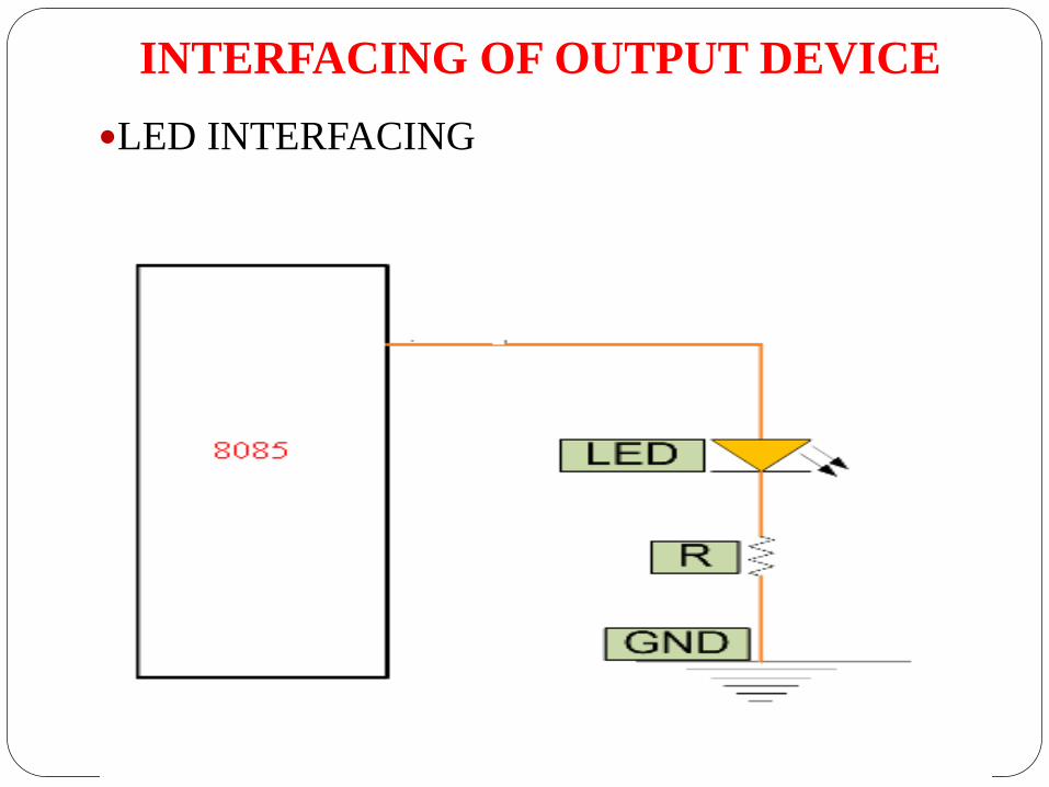
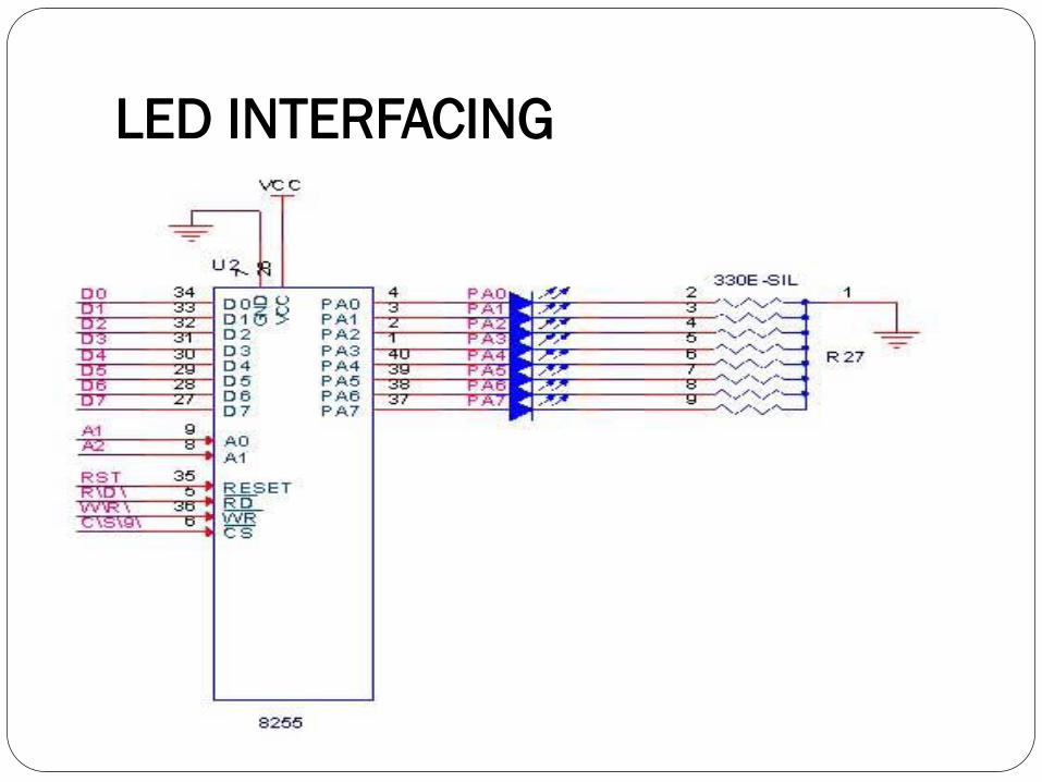
INTERFACING OF OUTPUT DEVICE
LED INTERFACING
Interrupts
An interrupt is considered to be an emergency signal that may
be serviced.
The Microprocessor may respond to it as soon as possible.
When the Microprocessor receives an interrupt signal, it suspends
the currently executing program and jumps to an
Interrupt Service Routine (ISR) to respond to the incoming
interrupt.
Each interrupt will most probably have its own ISR.
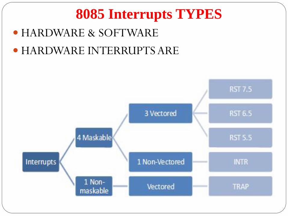
8085 Interrupts TYPES
HARDWARE & SOFTWARE
HARDWARE INTERRUPTS ARE
Interrupts
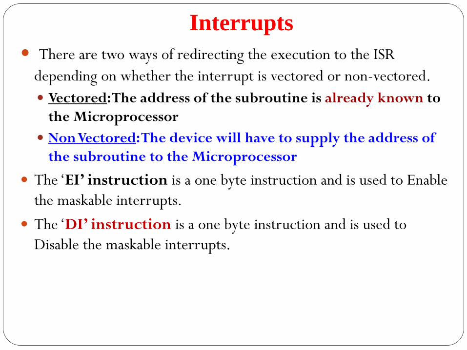
There are two ways of redirecting the execution to the ISR
depending on whether the interrupt is vectored or non-vectored.
Vectored: The address of the subroutine is already known to
the Microprocessor
Non Vectored: The device will have to supply the address of
the subroutine to the Microprocessor
The ‘EI’ instruction is a one byte instruction and is used to Enable
the maskable interrupts.
The ‘DI’ instruction is a one byte instruction and is used to
Disable the maskable interrupts.
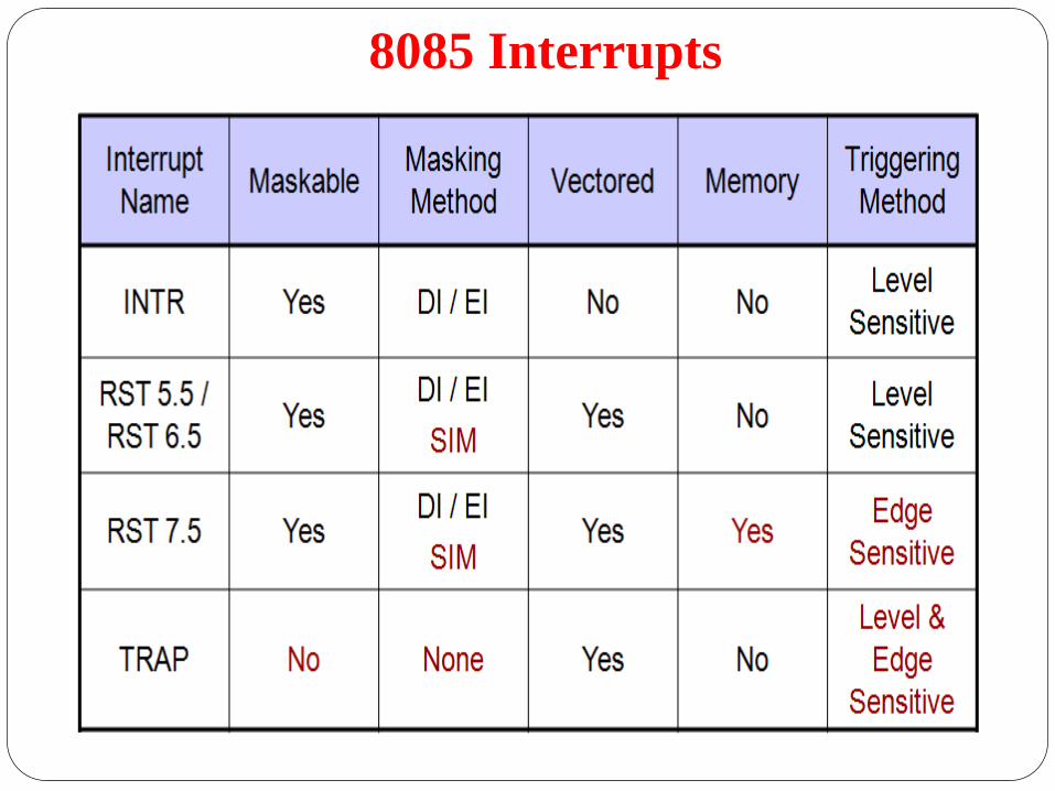
8085 Interrupts
8085 Interrupts
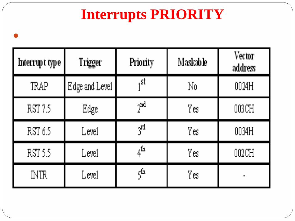
Interrupts PRIORITY
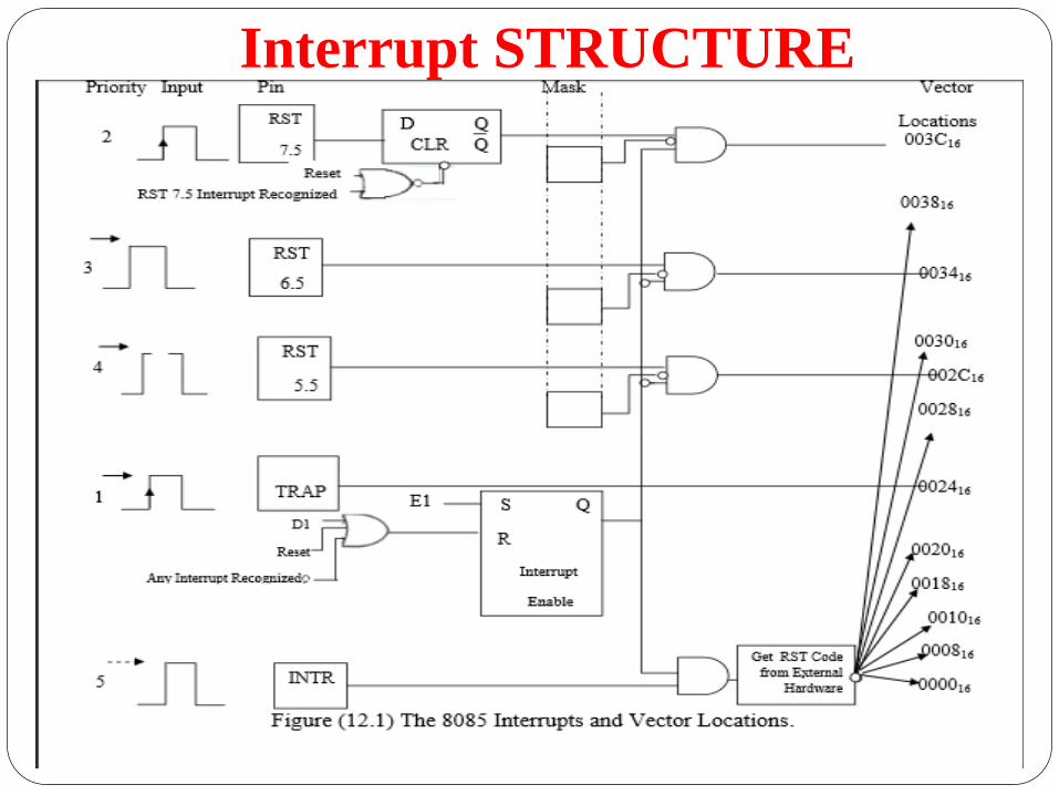
Interrupt STRUCTURE
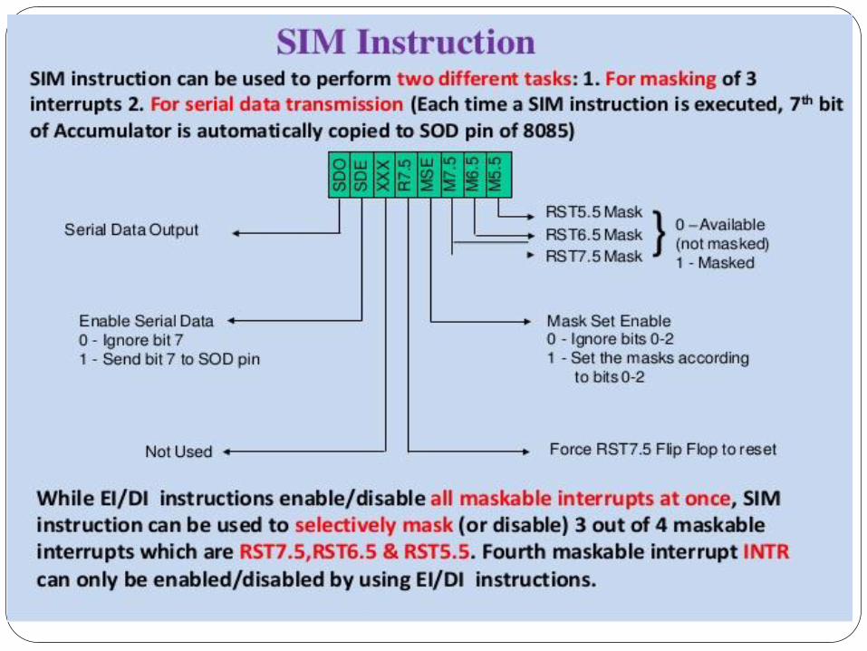
SIM
Interrupts
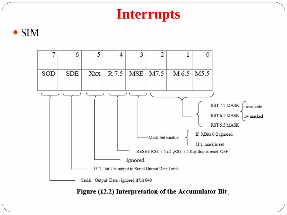
SIM
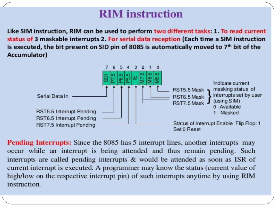
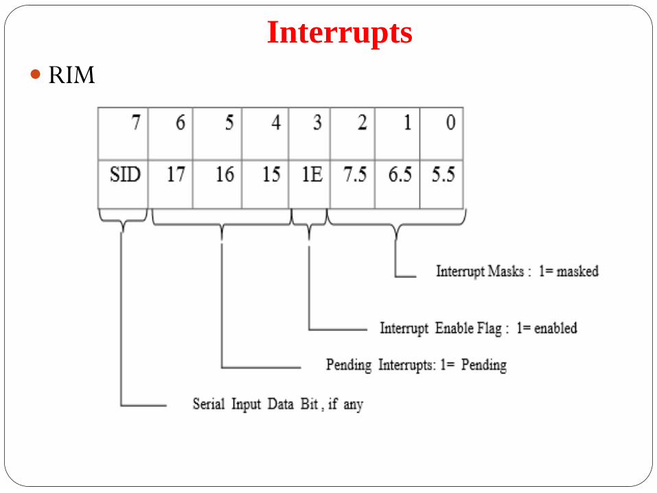
Interrupts
RIM
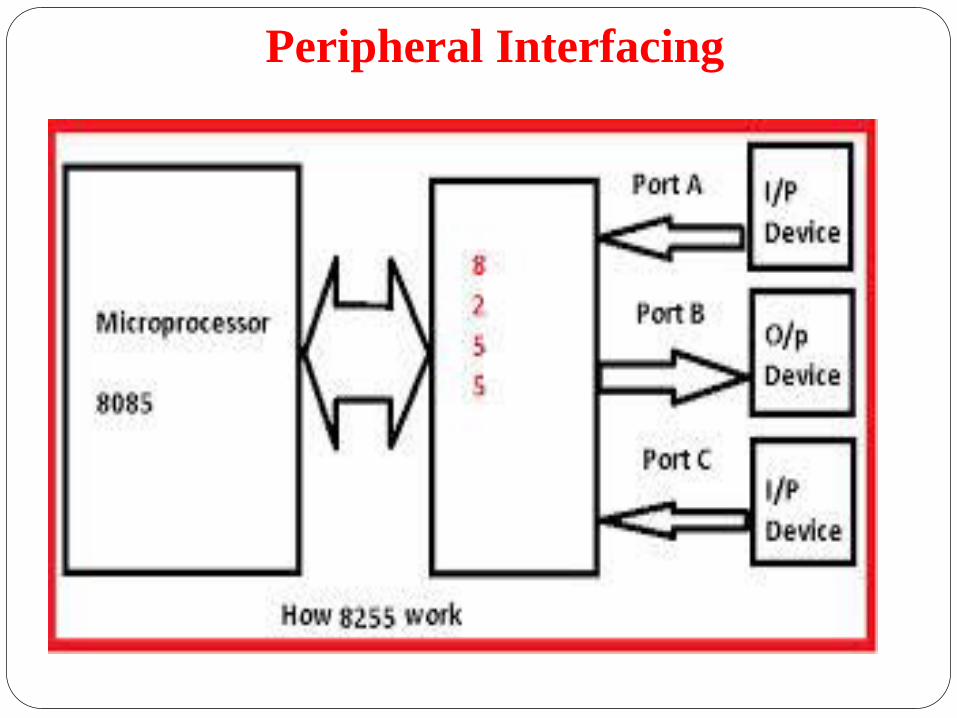
Peripheral Interfacing
8255 PIN
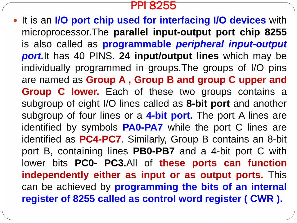
PPI 8255
It is an I/O port chip used for interfacing I/O devices with
microprocessor.The parallel input-output port chip 8255
is also called as programmable peripheral input-output
port.It has 40 PINS. 24 input/output lines which may be
individually programmed in groups.The groups of I/O pins
are named as Group A , Group B and group C upper and
Group C lower. Each of these two groups contains a
subgroup of eight I/O lines called as 8-bit port and another
subgroup of four lines or a 4-bit port. The port A lines are
identified by symbols PA0-PA7 while the port C lines are
identified as PC4-PC7. Similarly, Group B contains an 8-bit
port B, containing lines PB0-PB7 and a 4-bit port C with
lower bits PC0- PC3.All of these ports can function
independently either as input or as output ports. This
can be achieved by programming the bits of an internal
register of 8255 called as control word register ( CWR ).
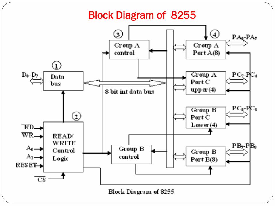
Block Diagram of 8255
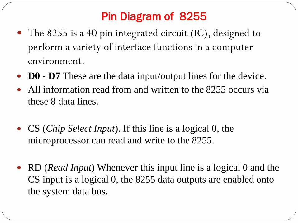
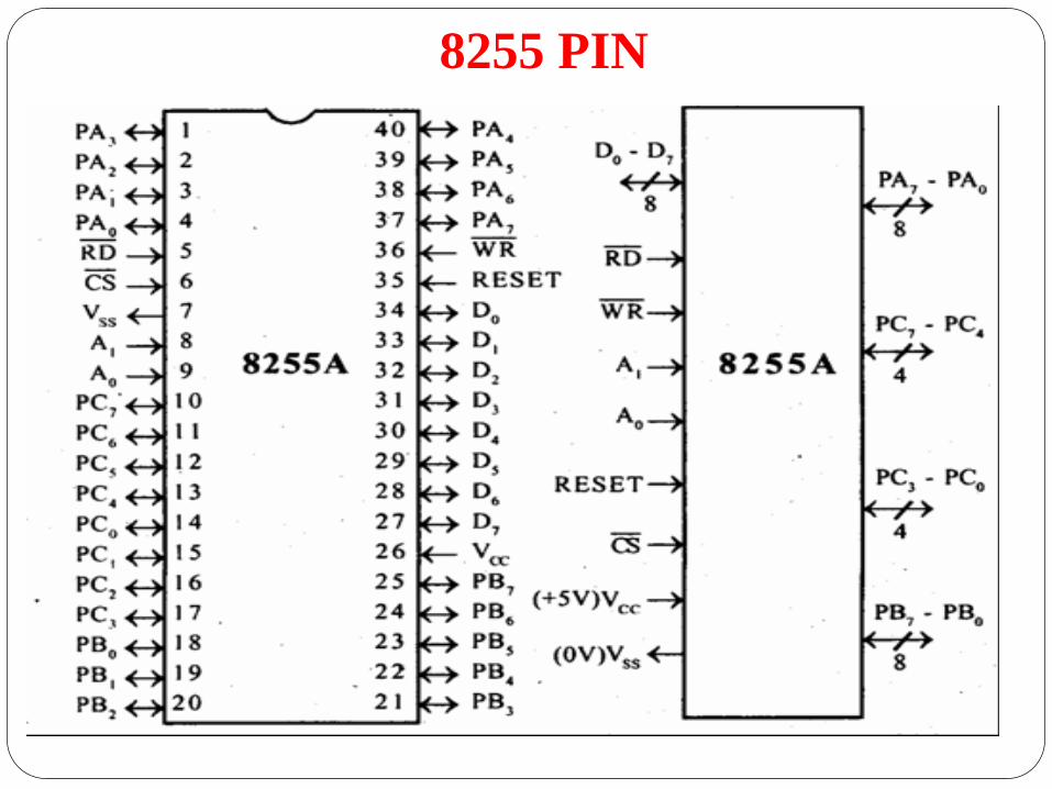
Pin Diagram of 8255
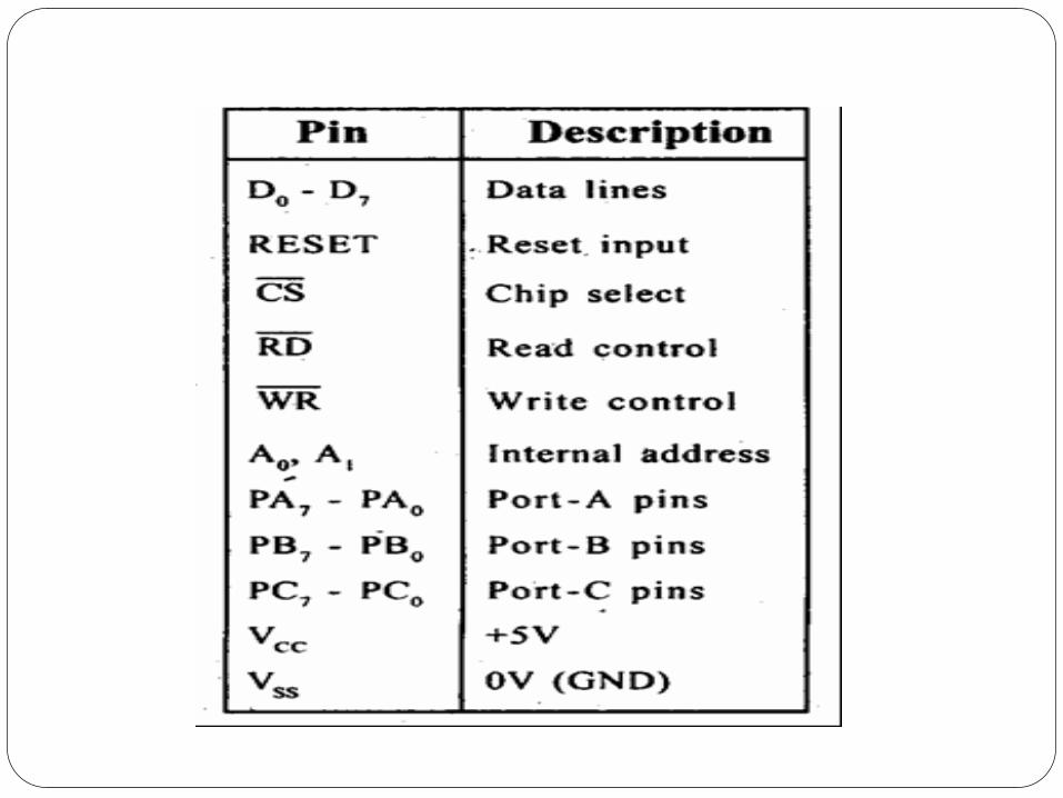
The 8255 is a 40 pin integrated circuit (IC), designed to
perform a variety of interface functions in a computer
environment.
D0 - D7 These are the data input/output lines for the device.
All information read from and written to the 8255 occurs via
these 8 data lines.
CS (Chip Select Input). If this line is a logical 0, the
microprocessor can read and write to the 8255.
RD (Read Input) Whenever this input line is a logical 0 and the
CS input is a logical 0, the 8255 data outputs are enabled onto
the system data bus.
Pin Diagram of 8255
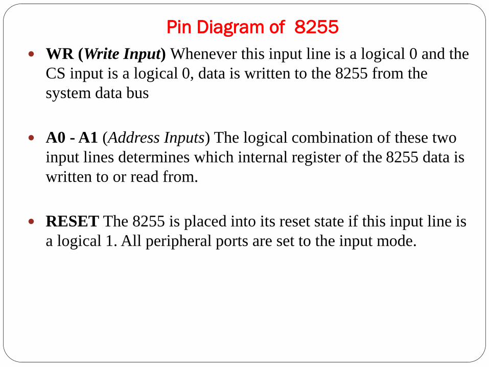
WR (Write Input) Whenever this input line is a logical 0 and the
CS input is a logical 0, data is written to the 8255 from the
system data bus
A0 - A1 (Address Inputs) The logical combination of these two
input lines determines which internal register of the 8255 data is
written to or read from.
RESET The 8255 is placed into its reset state if this input line is
a logical 1. All peripheral ports are set to the input mode.
Pin Diagram of 8255
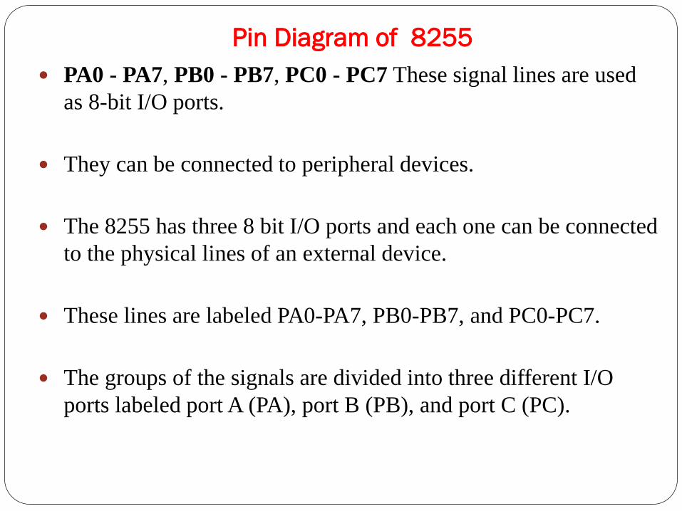
PA0 - PA7, PB0 - PB7, PC0 - PC7 These signal lines are used
as 8-bit I/O ports.
They can be connected to peripheral devices.
The 8255 has three 8 bit I/O ports and each one can be connected
to the physical lines of an external device.
These lines are labeled PA0-PA7, PB0-PB7, and PC0-PC7.
The groups of the signals are divided into three different I/O
ports labeled port A (PA), port B (PB), and port C (PC).
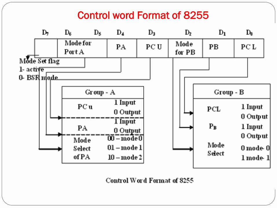
Control word Format of 8255
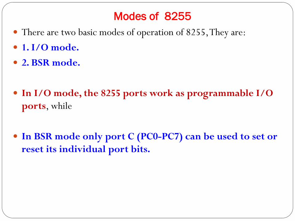
Modes of 8255
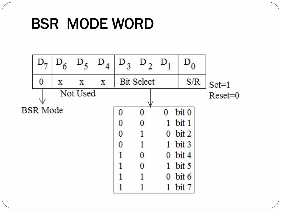
There are two basic modes of operation of 8255, They are:
1. I/O mode.
2. BSR mode.
In I/O mode, the 8255 ports work as programmable I/O
ports, while
In BSR mode only port C (PC0-PC7) can be used to set or
reset its individual port bits.
Modes of 8255
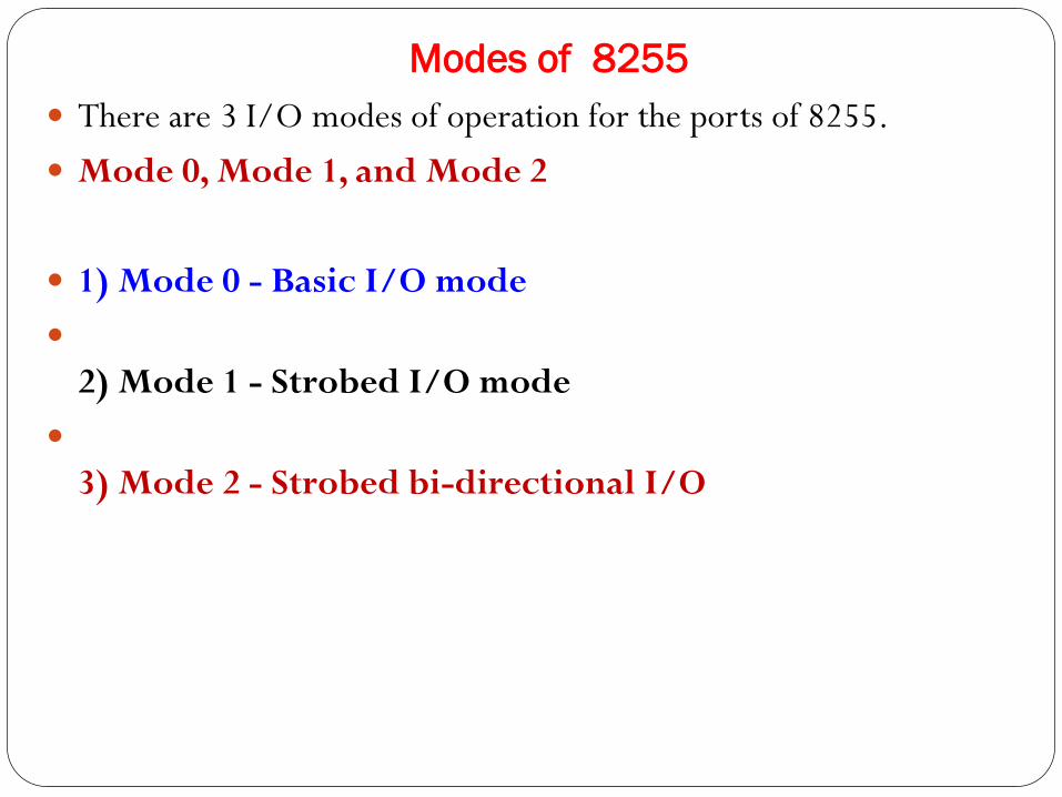
There are 3 I/O modes of operation for the ports of 8255.
Mode 0, Mode 1, and Mode 2
1) Mode 0 - Basic I/O mode
2) Mode 1 - Strobed I/O mode
3) Mode 2 - Strobed bi-directional I/O
Modes of 8255
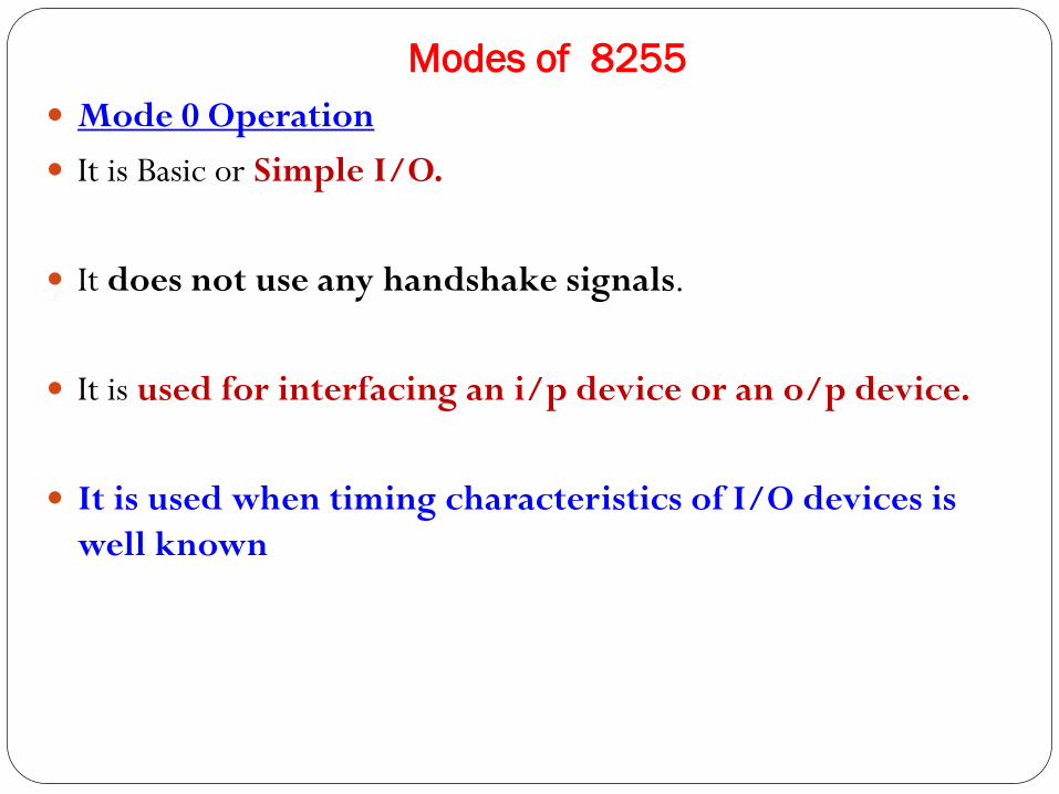
Mode 0 Operation
It is Basic or Simple I/O.
It does not use any handshake signals.
It is used for interfacing an i/p device or an o/p device.
It is used when timing characteristics of I/O devices is
well known
Modes of 8255
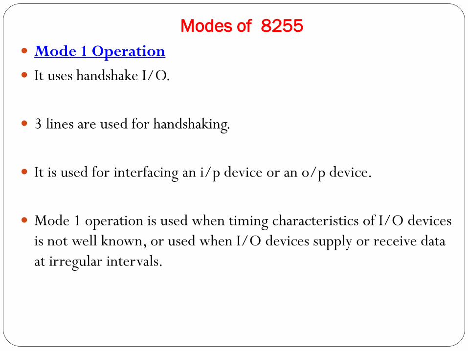
Mode 1 Operation
It uses handshake I/O.
3 lines are used for handshaking.
It is used for interfacing an i/p device or an o/p device.
Mode 1 operation is used when timing characteristics of I/O devices
is not well known, or used when I/O devices supply or receive data
at irregular intervals.
Modes of 8255
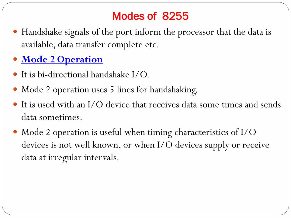
Handshake signals of the port inform the processor that the data is
available, data transfer complete etc.
Mode 2 Operation
It is bi-directional handshake I/O.
Mode 2 operation uses 5 lines for handshaking.
It is used with an I/O device that receives data some times and sends
data sometimes.
Mode 2 operation is useful when timing characteristics of I/O
devices is not well known, or when I/O devices supply or receive
data at irregular intervals.
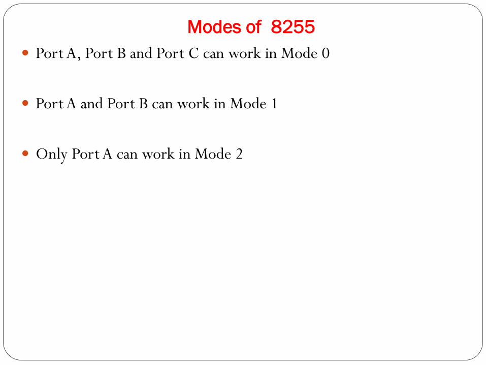
Modes of 8255
Port A, Port B and Port C can work in Mode 0
Port A and Port B can work in Mode 1
Only Port A can work in Mode 2
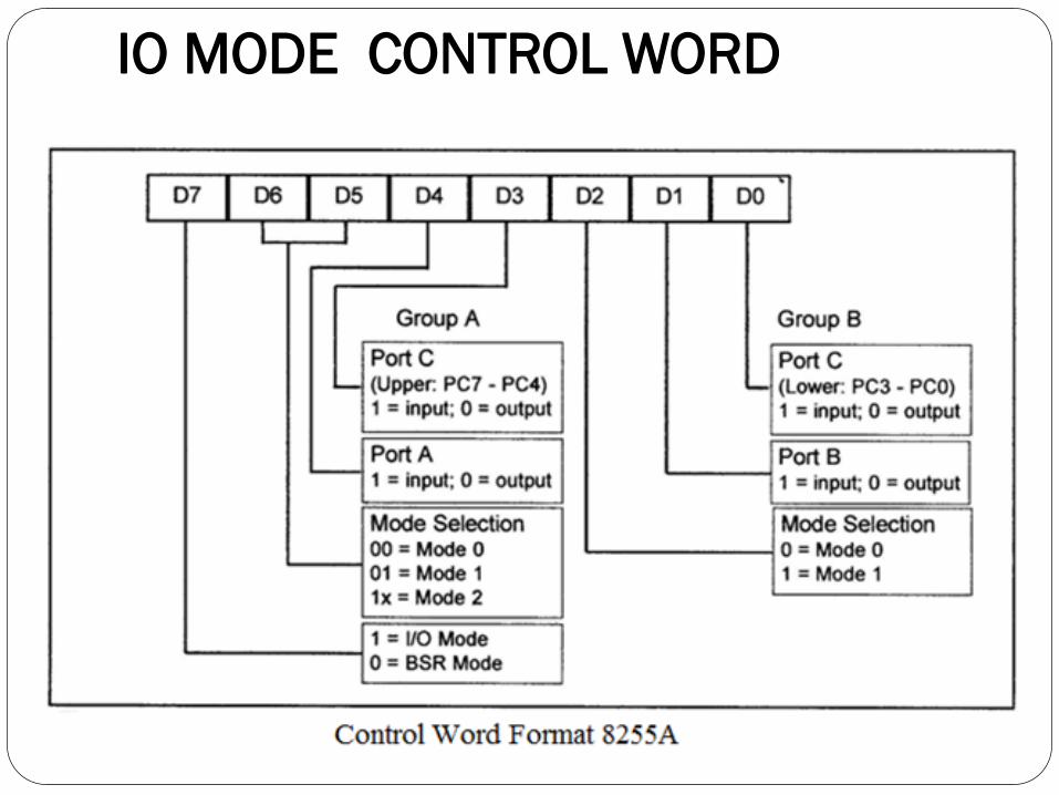
IO MODE CONTROL WORD
BSR MODE WORD
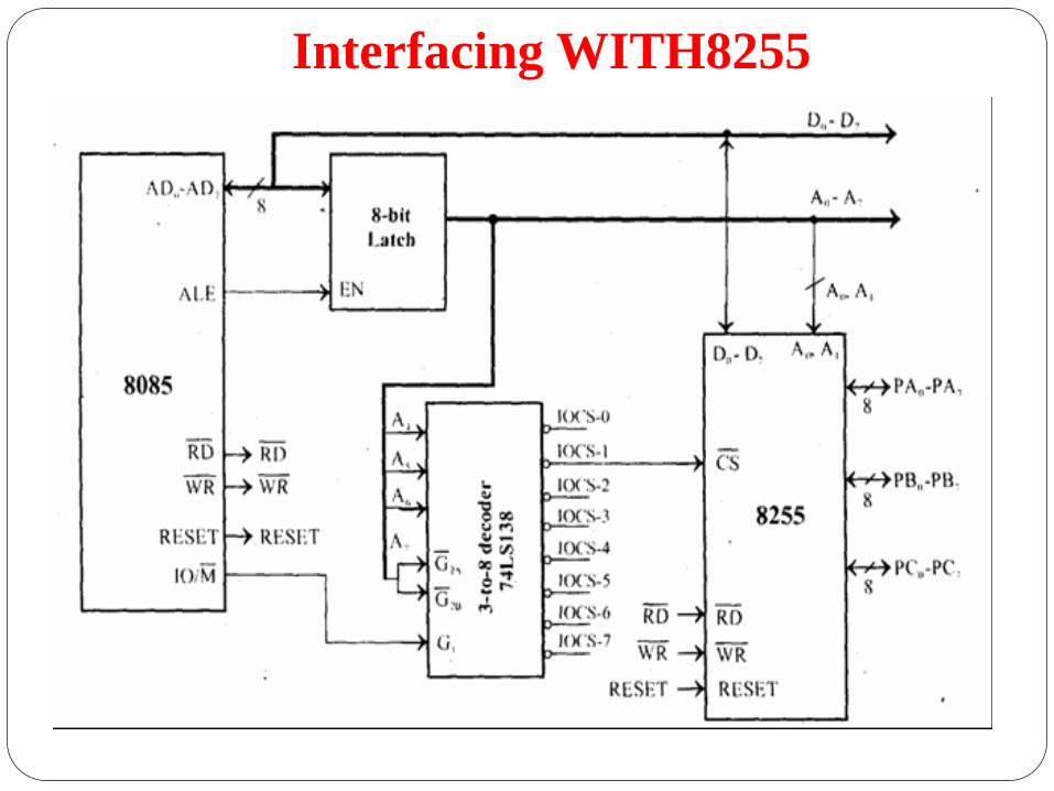
Interfacing WITH8255
LED INTERFACING
A/D Interfacing
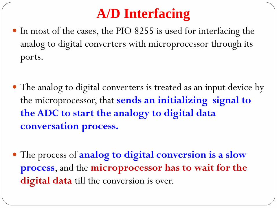
In most of the cases, the PIO 8255 is used for interfacing the
analog to digital converters with microprocessor through its
ports.
The analog to digital converters is treated as an input device by
the microprocessor, that sends an initializing signal to
the ADC to start the analogy to digital data
conversation process.
The process of analog to digital conversion is a slow
process, and the microprocessor has to wait for the
digital data till the conversion is over.
A/D Interfacing
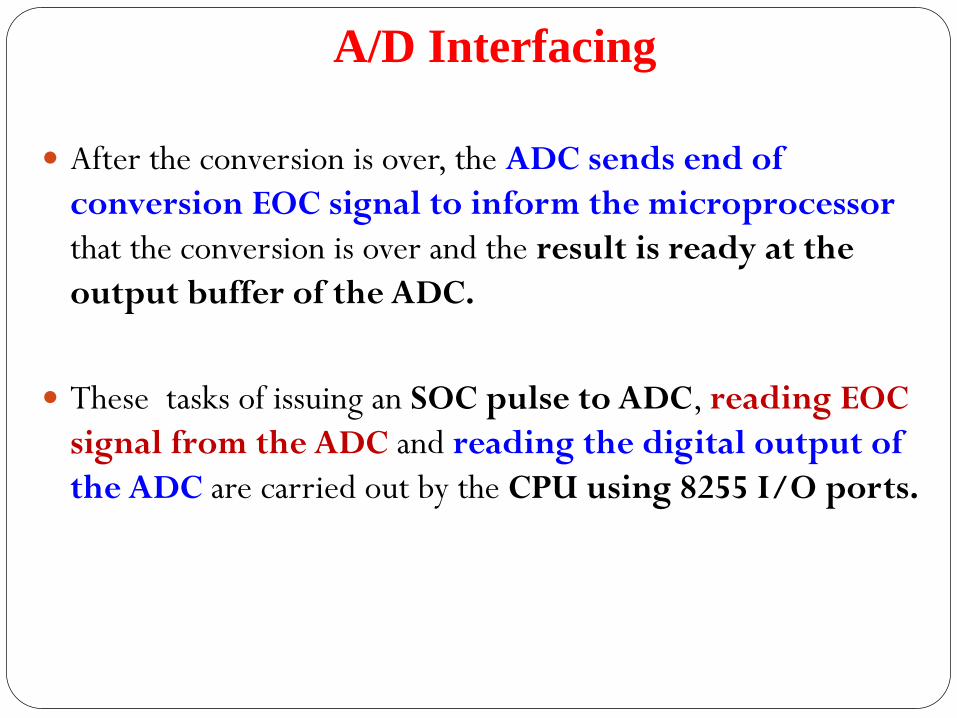
After the conversion is over, the ADC sends end of
conversion EOC signal to inform the microprocessor
that the conversion is over and the result is ready at the
output buffer of the ADC.
These tasks of issuing an SOC pulse to ADC, reading EOC
signal from the ADC and reading the digital output of
the ADC are carried out by the CPU using 8255 I/O ports.
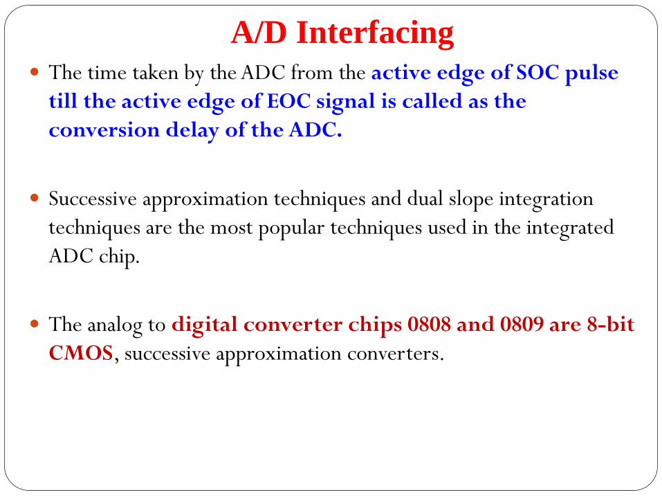
A/D Interfacing The time taken by the ADC from the active edge of SOC pulse
till the active edge of EOC signal is called as the
conversion delay of the ADC.
Successive approximation techniques and dual slope integration
techniques are the most popular techniques used in the integrated
ADC chip.
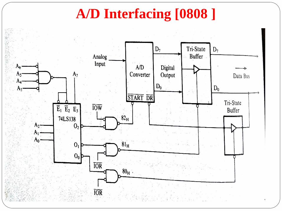
The analog to digital converter chips 0808 and 0809 are 8-bit
CMOS, successive approximation converters.
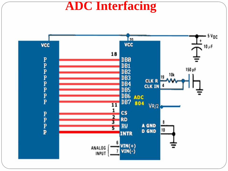
ADC 0804
ADC Interfacing CS :Active low input used to activate the ADC0804
chip.
RD (data enable) : Active low input used to get
converted data out of the ADC0804 chip. When CS = 0,
if a high-to-low pulse is applied to the RD pin, the 8-bit
digital output shows up at the D0-D7 data pins.
WR (start conversion): Active low input used to inform
the ADC0804 to start the conversion process. If CS = 0
when WR makes a low-to-high transition, the ADC0804
starts converting the analog input value of Vin to an 8-
bit digital number. When the data conversion is
complete, the INTR pin is forced low by the ADC0804.
ADC Interfacing CLK IN and CLK R : Connect to external capacitor and
resistor for self-clocking, f = 1/(1.1RC). The clock affect
the conversion time and this time cannot be faster than
110 micros.
INTR (end of conversion) This is an active low output
pin. When the conversion is finished, it goes low to
signal the CPU that the converted data is ready to be
picked up. After INTR goes low, we make CS = 0 and
send a high-to-low pulse to the RD pin to get the data
out of the ADC0804 chip.
ADC Interfacing
Vin (+) and Vin (-) :These are the differential analog inputs
where Vin = Vin (+) -Vin (-). Often the Vin (-) pin is
connected to ground and the Vin (+) pin is used as the
analog input to be converted to digital.
VCC : This is the +5V power supply. It is also used as a
reference voltage when the Vref/2 (pin 9) input is open.
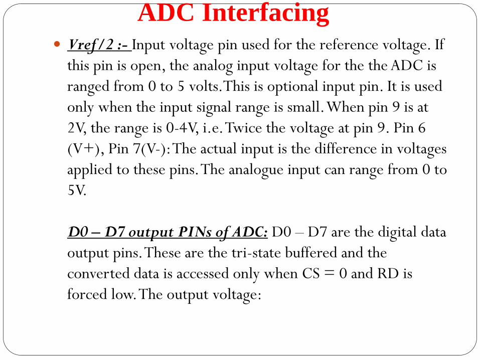
ADC Interfacing Vref/2 :- Input voltage pin used for the reference voltage. If
this pin is open, the analog input voltage for the the ADC is
ranged from 0 to 5 volts.This is optional input pin. It is used
only when the input signal range is small. When pin 9 is at
2V, the range is 0-4V, i.e. Twice the voltage at pin 9. Pin 6
(V+), Pin 7(V-): The actual input is the difference in voltages
applied to these pins. The analogue input can range from 0 to
5V.
D0 – D7 output PINs of ADC: D0 – D7 are the digital data
output pins. These are the tri-state buffered and the
converted data is accessed only when CS = 0 and RD is
forced low. The output voltage:
ADC Interfacing
A/D Interfacing [0808 ]
D/A INTERFACING
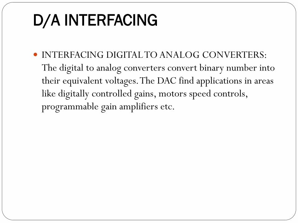
INTERFACING DIGITAL TO ANALOG CONVERTERS:
The digital to analog converters convert binary number into
their equivalent voltages. The DAC find applications in areas
like digitally controlled gains, motors speed controls,
programmable gain amplifiers etc.
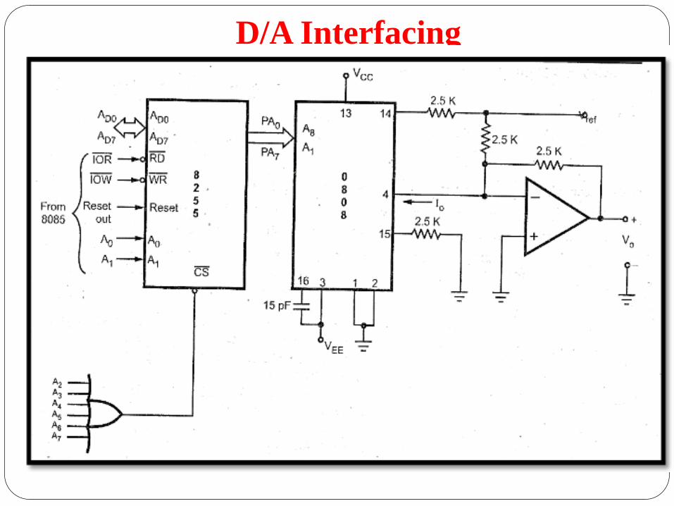
D/A Interfacing
MODULE 4
EMBEDDED SYSTEM
EMBEDDED SYSTEM
System
A system is an arrangement in which all its unit
assemble work together according to a set of rules.
It can also be defined as a way of working,
organizing or doing one or many tasks according to
a fixed plan.
For example, a watch is a time displaying system.
Its components follow a set of rules to show time. If
one of its parts fails, the watch will stop working. So
we can say, in a system, all its subcomponents
depend on each other
EMBEDDED SYSTEM
Embedded means something that is attached to
another thing. An embedded system can be
thought of as a computer hardware system having
software embedded in it. An embedded system
can be an independent system or it can be a part
of a large system. An embedded system is a
microcontroller or microprocessor based system
which is designed to perform a specific task. For
example, a fire alarm is an embedded system; it
will sense only smoke.
COMPONENTS
It has hardware.
It has application software.
It has Real Time Operating system (RTOS)
that supervises the application software and
provide mechanism to let the processor run a
process as per scheduling by following a plan to
control the latencies. RTOS defines the way the
system works. It sets the rules during the
execution of application program. A small scale
embedded system may not have RTOS.
Characteristics of an Embedded
System
Single-functioned – An embedded system
usually performs a specialized operation and
does the same repeatedly. For example: A pager
always functions as a pager.
Tightly constrained – All computing systems
have constraints on design metrics, but those on
an embedded system can be especially tight
Reactive and Real time – Many embedded
systems must continually react to changes in the
system's environment and must compute certain
results in real time without any delay.
Characteristics
Microprocessors based – It must be
microprocessor or microcontroller based.
Memory – It must have a memory, as its
software usually embeds in ROM. It does not
need any secondary memories in the computer.
Connected – It must have connected
peripherals to connect input and output devices.
HW-SW systems – Software is used for more
features and flexibility. Hardware is used for
performance and security.

ADVANTAGES & DISADVANTAGES
ADVANTAGES DISADVANTAGES
Easily
Customizable
Low power
consumption
Low cost
Enhanced
performance
High development
effort
Larger time to
market
175 ICET
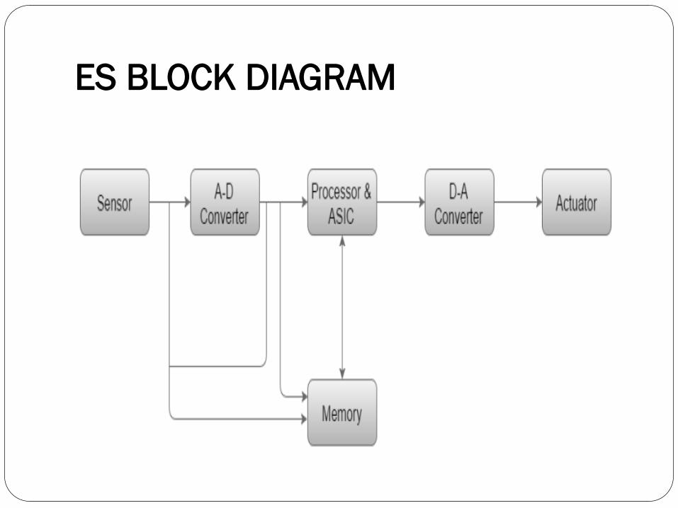
ES BLOCK DIAGRAM
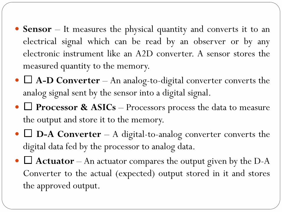
Sensor – It measures the physical quantity and converts it to an
electrical signal which can be read by an observer or by any
electronic instrument like an A2D converter. A sensor stores the
measured quantity to the memory.
A-D Converter – An analog-to-digital converter converts the
analog signal sent by the sensor into a digital signal.
Processor & ASICs – Processors process the data to measure
the output and store it to the memory.
D-A Converter – A digital-to-analog converter converts the
digital data fed by the processor to analog data.
Actuator – An actuator compares the output given by the D-A
Converter to the actual (expected) output stored in it and stores
the approved output.

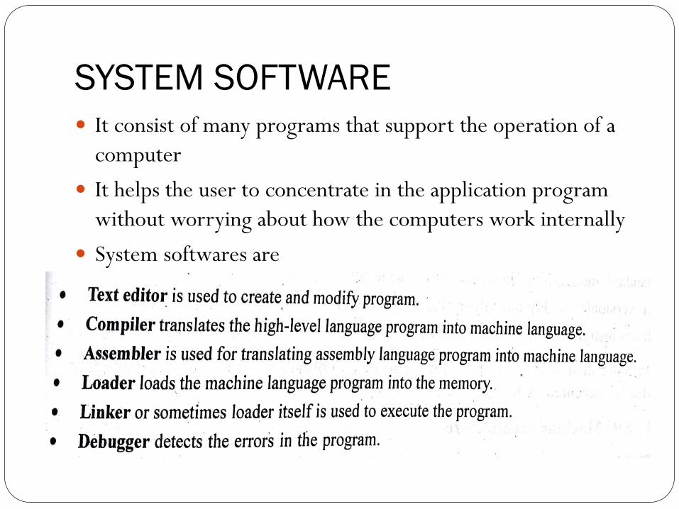
SYSTEM SOFTWARE
It consist of many programs that support the operation of a
computer
It helps the user to concentrate in the application program
without worrying about how the computers work internally
System softwares are
ASSEMBLER
A computer will not understand any program written in a
language, other than its machine language. The programs
written in other languages must be translated into the
machine language. Such translation is performed with the
help of software. A program which translates an assembly
language program into a machine language program is called
an assembler. If an assembler which runs on a computer and
produces the machine codes for the same computer then it is
called self assembler or resident assembler. If an assembler
that runs on a computer and produces the machine codes for
other computer then it is called Cross Assembler
COMPILER
It is a program which translates a high level language
program into a machine language program. A compiler is
more intelligent than an assembler. It checks all kinds of
limits, ranges, errors etc. But its program run time is more
and occupies a larger part of the memory. It has slow speed.
Because a compiler goes through the entire program and
then translates the entire program into machine codes. If a
compiler runs on a computer and produces the machine
codes for the same computer then it is known as a self
compiler or resident compiler. On the other hand, if a
compiler runs on a computer and produces the machine
codes for other computer then it is known as a cross
compiler.
LINKERS
In high level languages, some built in header files
or libraries are stored. These libraries are
predefined and these contain basic functions
which are essential for executing the program.
These functions are linked to the libraries by a
program called Linker. If linker does not find a
library of a function then it informs to compiler
and then compiler generates an error. The
compiler automatically invokes the linker as the
last step in compiling a program.
LOADER
Loader is a program that loads machine codes of a program
into the system memory. In Computing, a loader is the part
of an Operating System that is responsible for loading
programs. It is one of the essential stages in the process of
starting a program. Because it places programs into memory
and prepares them for execution. Loading a program involves
reading the contents of executable file into memory. Once
loading is complete, the operating system starts the program
by passing control to the loaded program code. All operating
systems that support program loading have loaders. In many
operating systems the loader is permanently resident in
memory.
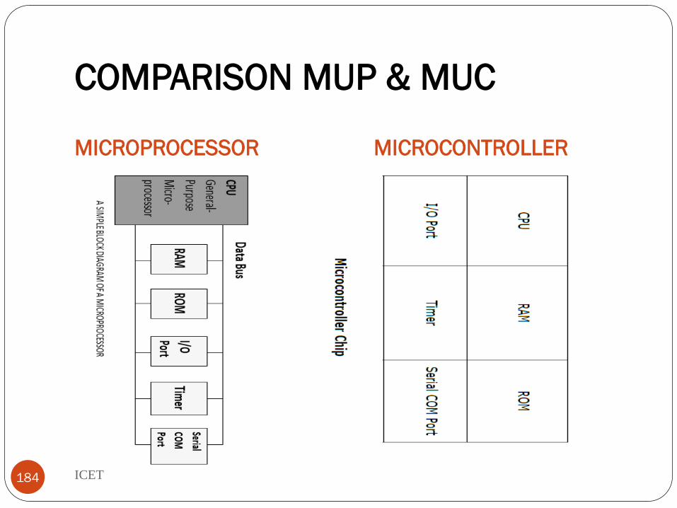
COMPARISON MUP & MUC
MICROPROCESSOR MICROCONTROLLER
184 ICET
Recent trends in Embedded
systems
With the fast developments in semiconductor industry and
VLSI technology ,one can find tremendous changes in the
embedded system design in terms of processor speed , power
,communication interfaces including network capabilities and
software developments like operating systems and
programming languages etc
Processor speed and Power
Communication interfaces
Operating systems
Programming Langauage
Challenges in Embedded Systems
1. Amount and type of hardware needed.
Optimizing various hardware elements for a particular
design.
2. Taking into account the design metrics
Design metrics examples –power dissipation, physical size,
number of gates and engineering, prototype development
and manufacturing costs.
3. Optimizing the Power Dissipation.
Clock Rate Reduction and Operating Voltage Reduction
4. Disable use of certain structural units of the processor to
reduce power dissipation the processor to reduce power
dissipation.
Control of power requirement, for example, by screen
auto‐brightness control
5. Process Deadlines
6. Flexibility and Upgradeability
7. Reliability
8. Testing, Verification and Validation
Real‐time embedded systems
An embedded system which gives the required output in a
specified time or which strictly follows the time dead lines
for completion of a task is known as a Real time system.
i.e a Real Time system , in addition to functional
correctness, also satisfies the time constraints .
There are two types of Real time systems.(i) Soft real time
system and (ii) Hard
Soft Real Real time system
A Real time system in which ,the violation of time
constraints will cause only the degraded quality, but the
system can continue to operate is known as a Soft real time
system.
In soft real‐time systems, the design focus is to offer a
guaranteed bandwidth to each real‐time task and to
distribute the resources to the tasks.
Ex: A Microwave Oven , washing machine ,TV remote
etc.
Hard Real‐Time system
A Real time system in which ,the violation of time
constraints will cause critica failure and loss of life or
property damage or catastrophe is known as a Hard Real
time system.
These systems usually interact directly with physical
hardware instead of through a human being
Ex: Deadline in a missile control embedded system ,
Delayed alarm during a Gas leakage , car airbag control
system , A delayed response in pacemakers ,Failure in
RADAR functioning

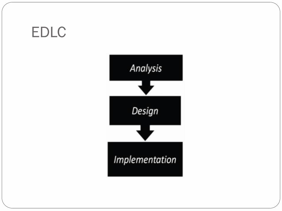
Embedded Product Development
Life Cycle (EDLC)
EDLC is Embedded Product Development Life Cycle
It is an Analysis – Design – Implementation based
problem solving approach for embedded systems
development.
There are three phases to Product development
EDLC
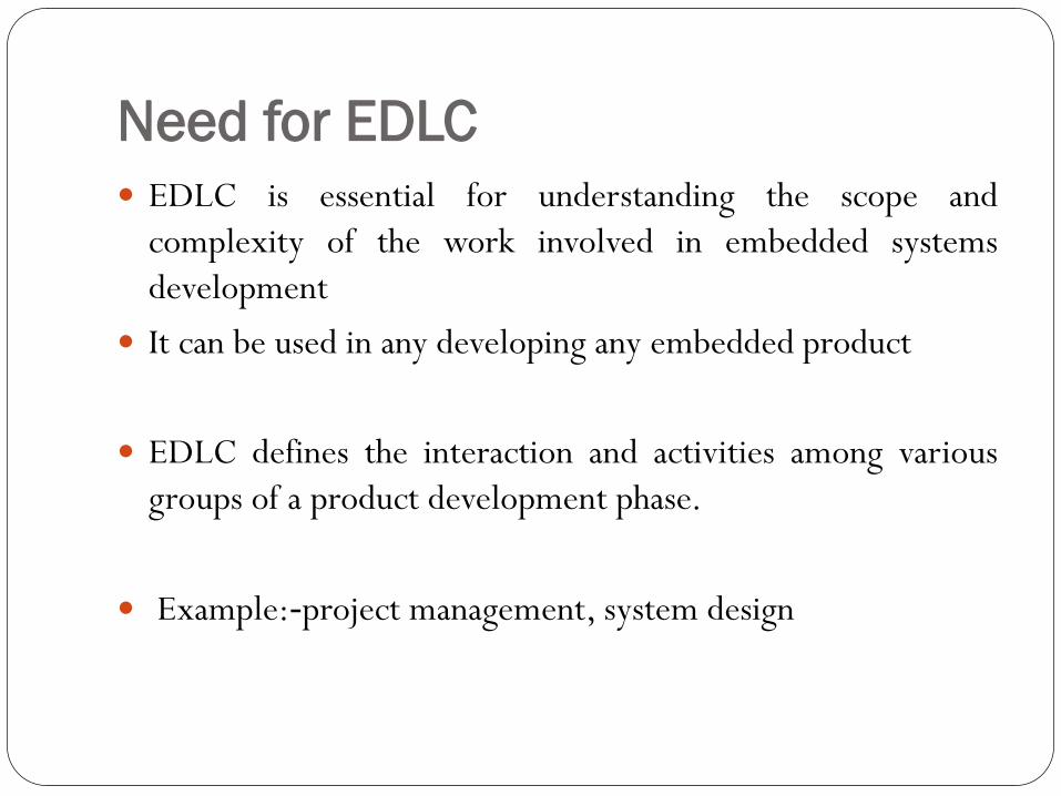
Need for EDLC
EDLC is essential for understanding the scope and
complexity of the work involved in embedded systems
development
It can be used in any developing any embedded product
EDLC defines the interaction and activities among various
groups of a product development phase.
Example:‐project management, system design

Objectives of EDLC
1. Ensure that high quality products are delivered to
user
2. Risk minimization defect prevention in product
development through project management
3. Maximize the productivity
Different Phases of EDLC:
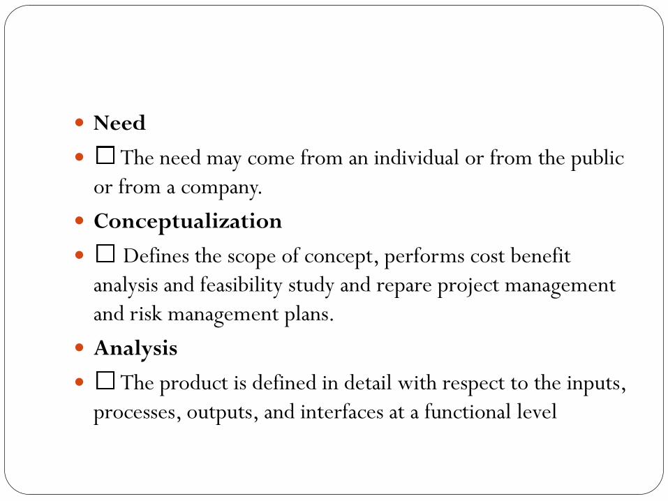
Need
The need may come from an individual or from the public
or from a company.
Conceptualization
Defines the scope of concept, performs cost benefit
analysis and feasibility study and repare project management
and risk management plans.
Analysis
The product is defined in detail with respect to the inputs,
processes, outputs, and interfaces at a functional level

Design
The design phase identifies application environment and
creates an overall architecture for the product.
Development and Testing
Development phase transforms the design into a
realizable product.
Deployment
Deployment is the process of launching the first fully
functional model of the product
in the market.
Support
The support phase deals with the operational and
maintenance of the product in the production environment.
Upgrades
Deals with the development of upgrades (new versions)
for the product which is already present in the market.
Retirement/Disposal
The retirement/disposal of the product is a gradual
process
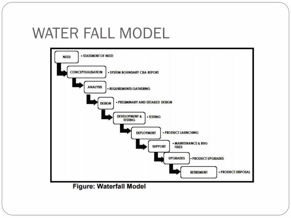
WATER FALL MODEL
Embedded Tool Chain System
Editor:
An editor is a software application used for editing plain
text.
Preprocessor:
Preprocessor directives are lines included i n the code of
programs that are not program statements but directives for
the preprocessor
Assembler
Assembler creates object code by translating mnemonics into
machine language.
Compiler
A compiler is a computer program (or set of programs) that
translates text written in a high level language into object
code
Linker:
A linker is a program that takes one or more objects
generated by compilers and assemblers and combine them
into a single executable program
Debuggers:
These tools are used for targeting, validating (error
checking and correction) and performance monitoring.
Loader
A Loader is an operating system utility that copies programs
from a storage device to main memory, where they can be
executed
Profilers
Profilers are used to find out what parts of the code have
been executed and how much time was spent in each part.
Test Coverage tool
A coverage tool can tell you what part of your code has
been exercised by a test run or an interactive session.
This helps you to identify dead code missing tests
MODULE 5
8051
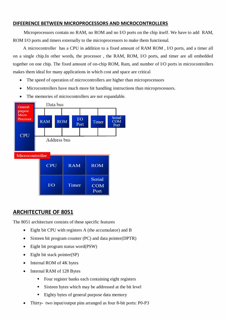
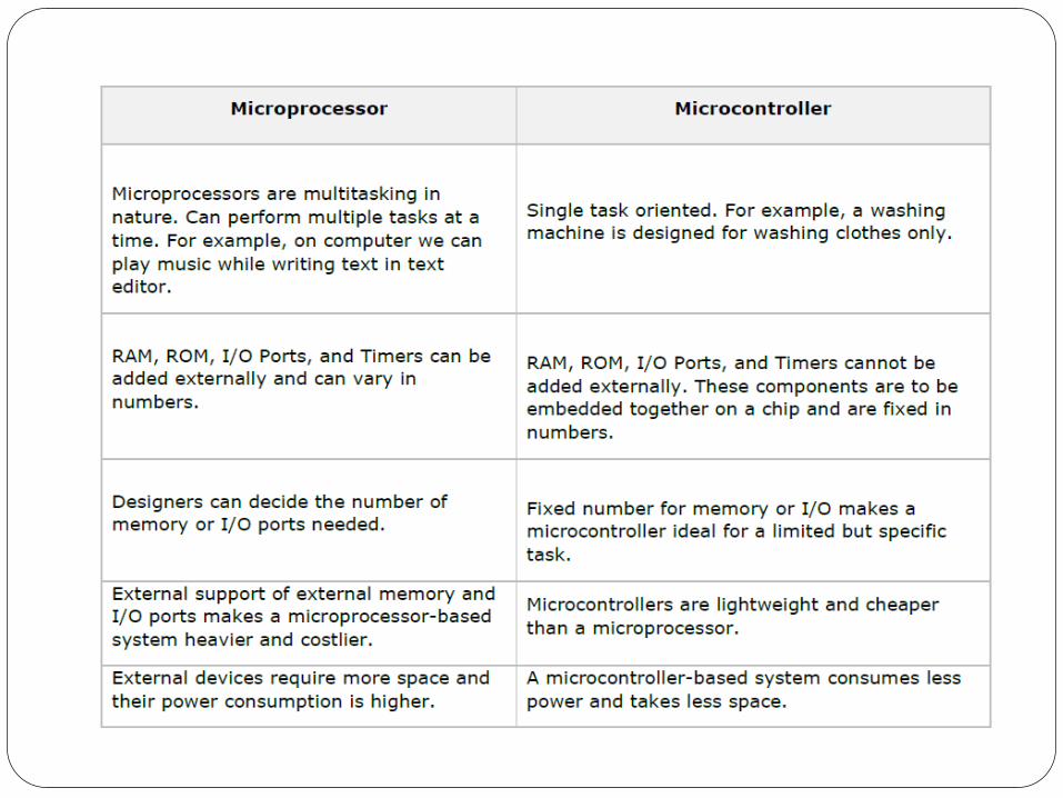
DIFEERENCE BETWEEN MICROPROCESSORS AND MICROCONTROLLERS
Microprocessors contain no RAM, no ROM and no I/O ports on the chip itself. We have to add RAM,
ROM I/O ports and timers externally to the microprocessors to make them functional.
A microcontroller has a CPU in addition to a fixed amount of RAM ROM , I/O ports, and a timer all
on a single chip.In other words, the processor , the RAM, ROM, I/O ports, and timer are all embedded
together on one chip. The fixed amount of on-chip ROM, Ram, and number of I/O ports in microcontrollers
makes them ideal for many applications in which cost and space are critical
The speed of operation of microcontrollers are higher than microprocessors
Microcontrollers have much more bit handling instructions than microprocessors.
The memories of microcontrollers are not expandable.
ARCHITECTURE OF 8051
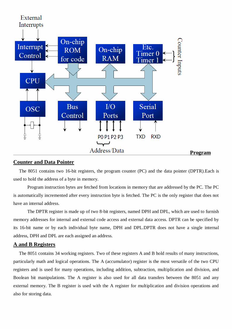
The 8051 architecture consists of these specific features
Eight bit CPU with registers A (the accumulator) and B
Sixteen bit program counter (PC) and data pointer(DPTR)
Eight bit program status word(PSW)
Eight bit stack pointer(SP)
Internal ROM of 4K bytes
Internal RAM of 128 Bytes
Four register banks each containing eight registers
Sixteen bytes which may be addressed at the bit level
Eighty bytes of general purpose data memory
Thirty- two input/output pins arranged as four 8-bit ports: P0-P3
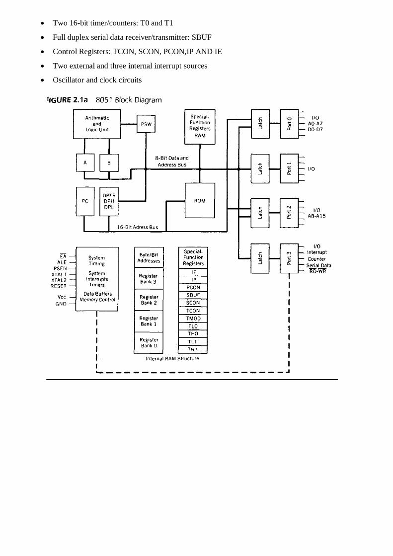
Two 16-bit timer/counters: T0 and T1
Full duplex serial data receiver/transmitter: SBUF
Control Registers: TCON, SCON, PCON,IP AND IE
Two external and three internal interrupt sources
Oscillator and clock circuits
Program
Counter and Data Pointer
The 8051 contains two 16-bit registers, the program counter (PC) and the data pointer (DPTR).Each is
used to hold the address of a byte in memory.
Program instruction bytes are fetched from locations in memory that are addressed by the PC. The PC
is automatically incremented after every instruction byte is fetched. The PC is the only register that does not
have an internal address.
The DPTR register is made up of two 8-bit registers, named DPH and DPL, which are used to furnish
memory addresses for internal and external code access and external data access. DPTR can be specified by
its 16-bit name or by each individual byte name, DPH and DPL.DPTR does not have a single internal
address, DPH and DPL are each assigned an address.
A and B Registers
The 8051 contains 34 working registers. Two of these registers A and B hold results of many instructions,
particularly math and logical operations. The A (accumulator) register is the most versatile of the two CPU
registers and is used for many operations, including addition, subtraction, multiplication and division, and
Boolean bit manipulations. The A register is also used for all data transfers between the 8051 and any
external memory. The B register is used with the A register for multiplication and division operations and
also for storing data.
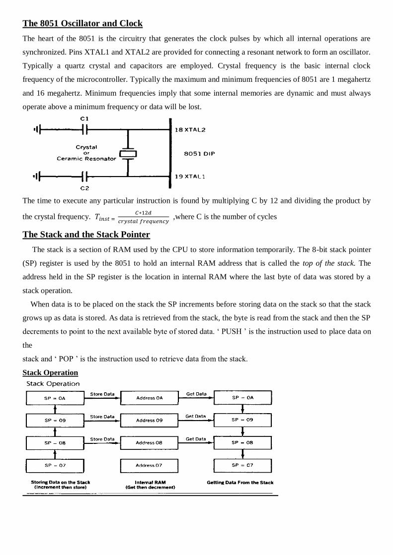
The 8051 Oscillator and Clock
The heart of the 8051 is the circuitry that generates the clock pulses by which all internal operations are
synchronized. Pins XTAL1 and XTAL2 are provided for connecting a resonant network to form an oscillator.
Typically a quartz crystal and capacitors are employed. Crystal frequency is the basic internal clock
frequency of the microcontroller. Typically the maximum and minimum frequencies of 8051 are 1 megahertz
and 16 megahertz. Minimum frequencies imply that some internal memories are dynamic and must always
operate above a minimum frequency or data will be lost.
The time to execute any particular instruction is found by multiplying C by 12 and dividing the product by
the crystal frequency.
,where C is the number of cycles
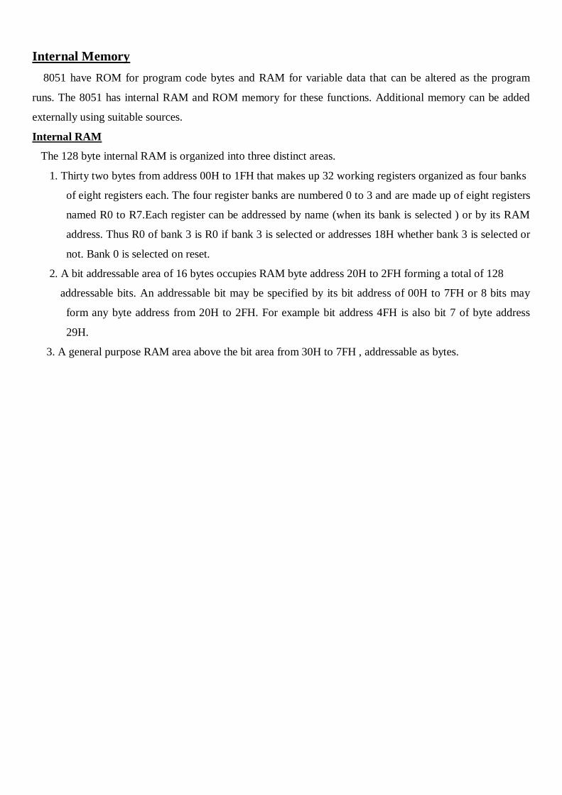
The Stack and the Stack Pointer
The stack is a section of RAM used by the CPU to store information temporarily. The 8-bit stack pointer
(SP) register is used by the 8051 to hold an internal RAM address that is called the top of the stack. The
address held in the SP register is the location in internal RAM where the last byte of data was stored by a
stack operation.
When data is to be placed on the stack the SP increments before storing data on the stack so that the stack
grows up as data is stored. As data is retrieved from the stack, the byte is read from the stack and then the SP
decrements to point to the next available byte of stored data. ‘ PUSH ’ is the instruction used to place data on
the
stack and ‘ POP ’ is the instruction used to retrieve data from the stack.
Stack Operation
Internal Memory
8051 have ROM for program code bytes and RAM for variable data that can be altered as the program
runs. The 8051 has internal RAM and ROM memory for these functions. Additional memory can be added
externally using suitable sources.
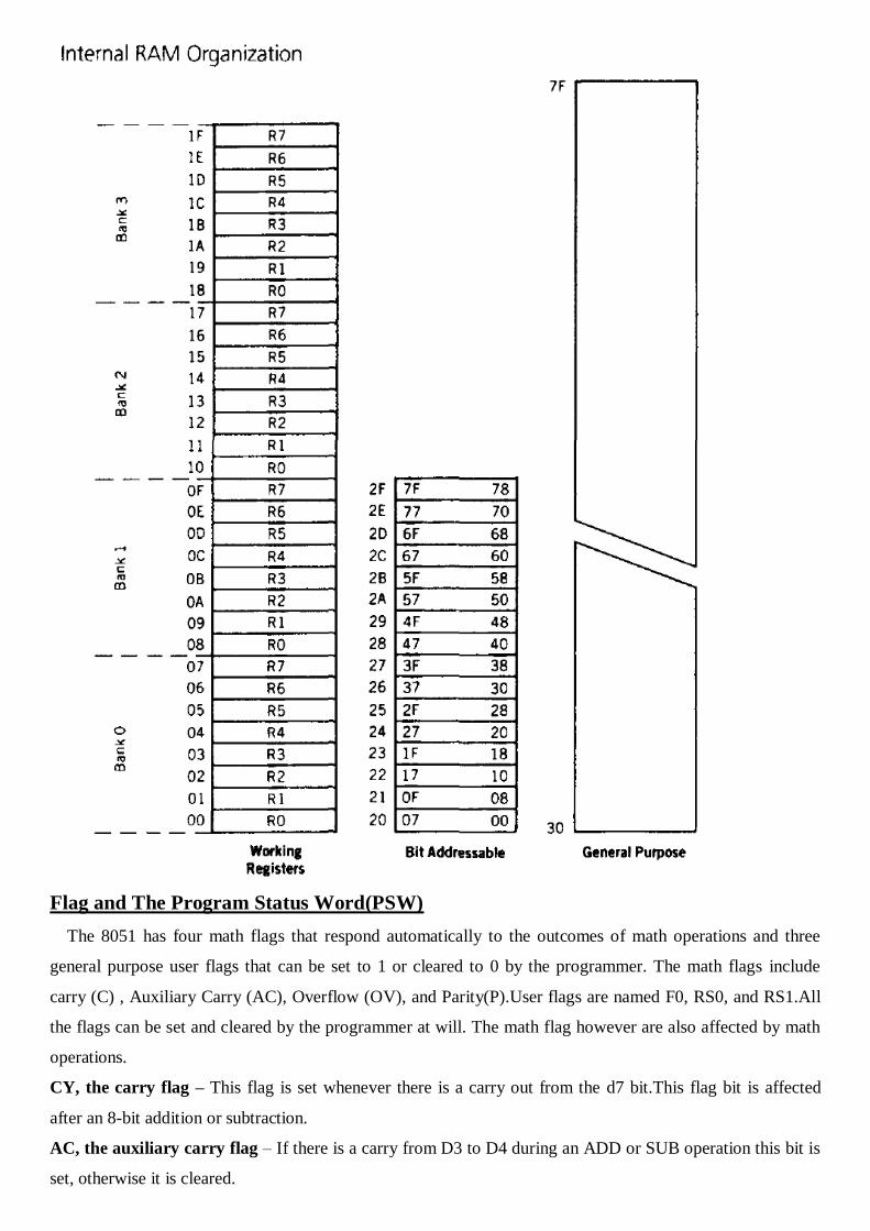
Internal RAM
The 128 byte internal RAM is organized into three distinct areas.
1. Thirty two bytes from address 00H to 1FH that makes up 32 working registers organized as four banks
of eight registers each. The four register banks are numbered 0 to 3 and are made up of eight registers
named R0 to R7.Each register can be addressed by name (when its bank is selected ) or by its RAM
address. Thus R0 of bank 3 is R0 if bank 3 is selected or addresses 18H whether bank 3 is selected or
not. Bank 0 is selected on reset.
2. A bit addressable area of 16 bytes occupies RAM byte address 20H to 2FH forming a total of 128
addressable bits. An addressable bit may be specified by its bit address of 00H to 7FH or 8 bits may
form any byte address from 20H to 2FH. For example bit address 4FH is also bit 7 of byte address
29H.
3. A general purpose RAM area above the bit area from 30H to 7FH , addressable as bytes.
Flag and The Program Status Word(PSW)
The 8051 has four math flags that respond automatically to the outcomes of math operations and three
general purpose user flags that can be set to 1 or cleared to 0 by the programmer. The math flags include
carry (C) , Auxiliary Carry (AC), Overflow (OV), and Parity(P).User flags are named F0, RS0, and RS1.All
the flags can be set and cleared by the programmer at will. The math flag however are also affected by math
operations.
CY, the carry flag – This flag is set whenever there is a carry out from the d7 bit.This flag bit is affected
after an 8-bit addition or subtraction.
AC, the auxiliary carry flag – If there is a carry from D3 to D4 during an ADD or SUB operation this bit is
set, otherwise it is cleared.
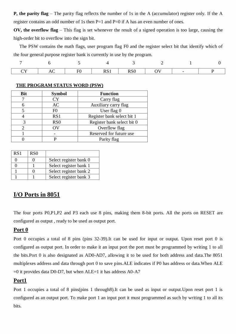
P, the parity flag – The parity flag reflects the number of 1s in the A (accumulator) register only. If the A
register contains an odd number of 1s then P=1 and P=0 if A has an even number of ones.
OV, the overflow flag – This flag is set whenever the result of a signed operation is too large, causing the
high-order bit to overflow into the sign bit.
The PSW contains the math flags, user program flag F0 and the register select bit that identify which of
the four general purpose register bank is currently in use by the program.
7 6 5 4 3 2 1 0
CY AC F0 RS1 RS0 OV - P
THE PROGRAM STATUS WORD (PSW)
Bit Symbol Function
7 CY Carry flag
6 AC Auxiliary carry flag
5 F0 User flag 0
4 RS1 Register bank select bit 1
3 RS0 Register bank select bit 0
2 OV Overflow flag
1 - Reserved for future use
0 P Parity flag
RS1 RS0 0 0 Select register bank 0
0 1 Select register bank 1
1 0 Select register bank 2
1 1 Select register bank 3
I/O Ports in 8051
The four ports P0,P1,P2 and P3 each use 8 pins, making them 8-bit ports. All the ports on RESET are
configured as output , ready to be used as output port.
Port 0
Port 0 occupies a total of 8 pins (pins 32-39).It can be used for input or output. Upon reset port 0 is
configured as output port. In order to make it an input port the port must be programmed by writing 1 to all
the bits.Port 0 is also designated as AD0-AD7, allowing it to be used for both address and data.The 8051
multiplexes address and data through port 0 to save pins.ALE indicates if P0 has address or data.When ALE
=0 it provides data D0-D7, but when ALE=1 it has address A0-A7
Port1
Port 1 occupies a total of 8 pins(pins 1 through8).It can be used as input or output.Upon reset port 1 is
configured as an output port. To make port 1 an input port it must programmed as such by writing 1 to all its
bits.
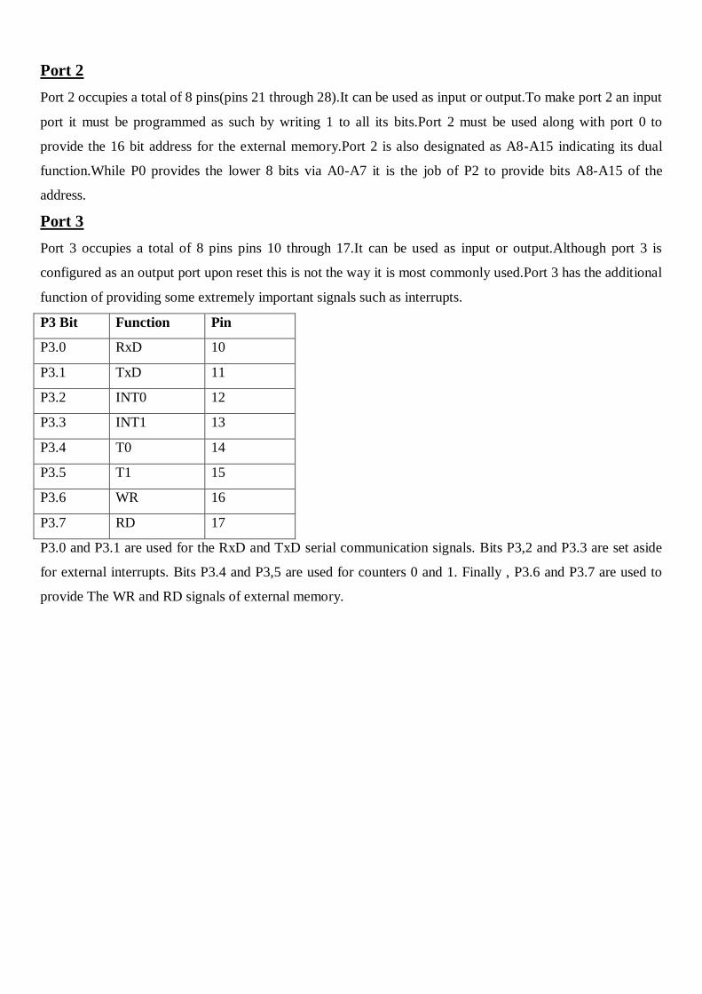
Port 2
Port 2 occupies a total of 8 pins(pins 21 through 28).It can be used as input or output.To make port 2 an input
port it must be programmed as such by writing 1 to all its bits.Port 2 must be used along with port 0 to
provide the 16 bit address for the external memory.Port 2 is also designated as A8-A15 indicating its dual
function.While P0 provides the lower 8 bits via A0-A7 it is the job of P2 to provide bits A8-A15 of the
address.
Port 3
Port 3 occupies a total of 8 pins pins 10 through 17.It can be used as input or output.Although port 3 is
configured as an output port upon reset this is not the way it is most commonly used.Port 3 has the additional
function of providing some extremely important signals such as interrupts.
P3 Bit Function Pin
P3.0 RxD 10
P3.1 TxD 11
P3.2 INT0 12
P3.3 INT1 13
P3.4 T0 14
P3.5 T1 15
P3.6 WR 16
P3.7 RD 17
P3.0 and P3.1 are used for the RxD and TxD serial communication signals. Bits P3,2 and P3.3 are set aside
for external interrupts. Bits P3.4 and P3,5 are used for counters 0 and 1. Finally , P3.6 and P3.7 are used to
provide The WR and RD signals of external memory.
Special Function Registers (SFRs)
Special Function Registers uses addresses from 80H to FFH. They are addressed much like internal RAM.
Some SFRs are also bit addressable. Not all of the addresses from 80H to FFH are used for SFRs and
attempting to use an address that is not defined or empty results in unpredictable results.
Interrupt Enable ( IE) Register
7 6 5 4 3 2 1 0
EA ---- ET2 ES ET1 EX1 ET0 EX0
(7 ) EA- Enable interrupt bit. Cleared to 0 by program to disable all interrupts. Set to 1 to permit individual
interrupts to be enabled by their enable bits.
(6) ---- Not implemented
(5) ET2 - Reserved for future use.
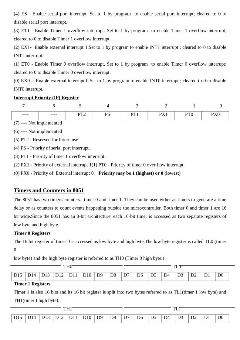
(4) ES - Enable serial port interrupt. Set to 1 by program to enable serial port interrupt; cleared to 0 to
disable serial port interrupt.
(3) ET1 - Enable Timer 1 overflow interrupt. Set to 1 by program to enable Timer 1 overflow interrupt;
cleared to 0 to disable Timer 1 overflow interrupt.
(2) EX1- Enable external interrupt 1.Set to 1 by program to enable INT1 interrupt.; cleared to 0 to disable
INT1 interrupt.
(1) ET0 - Enable Timer 0 overflow interrupt. Set to 1 by program to enable Timer 0 overflow interrupt;
cleared to 0 to disable Timer 0 overflow interrupt.
(0) EX0 - Enable external interrupt 0.Set to 1 by program to enable INT0 interrupt.; cleared to 0 to disable
INT0 interrupt.
Interrupt Priority (IP) Register
7 6 5 4 3 2 1 0
---- ---- PT2 PS PT1 PX1 PT0 PX0
(7) ---- Not implemented
(6) ---- Not implemented
(5) PT2 - Reserved for future use.
(4) PS - Priority of serial port interrupt.
(3) PT1 - Priority of timer 1 overflow interrupt.
(2) PX1 - Priority of external interrupt 1(1) PT0 - Priority of timer 0 over flow interrupt.
(0) PX0 - Priority of External interrupt 0. Priority may be 1 (highest) or 0 (lowest)
Timers and Counters in 8051
The 8051 has two timers/counters.; timer 0 and timer 1. They can be used either as timers to generate a time
delay or as counters to count events happening outside the microcontroller. Both timer 0 and timer 1 are 16
bit wide.Since the 8051 has an 8-bit architecture, each 16-bit timer is accessed as two separate registers of
low byte and high byte.
Timer 0 Registers
The 16 bit register of timer 0 is accessed as low byte and high byte.The low byte register is called TL0 (timer
0
low byte) and the high byte register is referred to as TH0 (Timer 0 high byte.)
TH0 TL0
D15 D14 D13 D12 D11 D10 D9 D8 D7 D6 D5 D4 D3 D2 D1 D0
Timer 1 Registers
Timer 1 is also 16 bits and its 16 bit register is split into two bytes referred to as TL1(timer 1 low byte) and
TH1(timer I high byte).
TH1 TL1
D15 D14 D13 D12 D11 D10 D9 D8 D7 D6 D5 D4 D3 D2 D1 D0
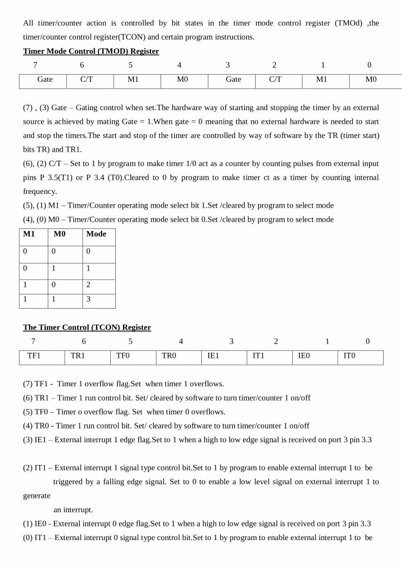
All timer/counter action is controlled by bit states in the timer mode control register (TMOd) ,the
timer/counter control register(TCON) and certain program instructions.
Timer Mode Control (TMOD) Register
7 6 5 4 3 2 1 0
Gate C/T M1 M0 Gate C/T M1 M0
(7) , (3) Gate – Gating control when set.The hardware way of starting and stopping the timer by an external
source is achieved by mating Gate = 1.When gate = 0 meaning that no external hardware is needed to start
and stop the timers.The start and stop of the timer are controlled by way of software by the TR (timer start)
bits TR) and TR1.
(6), (2) C/T – Set to 1 by program to make timer 1/0 act as a counter by counting pulses from external input
pins P 3.5(T1) or P 3.4 (T0).Cleared to 0 by program to make timer ct as a timer by counting internal
frequency.
(5), (1) M1 – Timer/Counter operating mode select bit 1.Set /cleared by program to select mode
(4), (0) M0 – Timer/Counter operating mode select bit 0.Set /cleared by program to select mode
M1 M0 Mode
0 0 0
0 1 1
1 0 2
1 1 3
The Timer Control (TCON) Register
7 6 5 4 3 2 1 0
TF1 TR1 TF0 TR0 IE1 IT1 IE0 IT0
(7) TF1 - Timer 1 overflow flag.Set when timer 1 overflows.
(6) TR1 – Timer 1 run control bit. Set/ cleared by software to turn timer/counter 1 on/off
(5) TF0 – Timer o overflow flag. Set when timer 0 overflows.
(4) TR0 - Timer 1 run control bit. Set/ cleared by software to turn timer/counter 1 on/off
(3) IE1 – External interrupt 1 edge flag.Set to 1 when a high to low edge signal is received on port 3 pin 3.3
(2) IT1 – External interrupt 1 signal type control bit.Set to 1 by program to enable external interrupt 1 to be
triggered by a falling edge signal. Set to 0 to enable a low level signal on external interrupt 1 to
generate
an interrupt.
(1) IE0 - External interrupt 0 edge flag.Set to 1 when a high to low edge signal is received on port 3 pin 3.3
(0) IT1 – External interrupt 0 signal type control bit.Set to 1 by program to enable external interrupt 1 to be
triggered by a falling edge signal. Set to 0 to enable a low level signal on external interrupt 1 to
generate
an interrupt.
IE0 and IE1 are used by the 8051 to keep track of the edge triggered interrupts only.In other words if the IT0
and It1 are 0 meaning that the hardwar interrupts are low level triggered , IE0 and IE1 are not used at all. The
IE0 and IE1 are used by the 8051 to latch the high to low edge transition on the INT0 and INT1 pins.
SBUF Register
SBUF is an 8-bit register used for serial communication in the 8051.For a byte of data to be transferred via
the TxD line it must be placed in the SBUF register.Similarly SBUF holds the byte of data when it is
received by the 8051’s RxD line.SBUF can be accessed like any other registers in the 8051.The moment a
byte is written into SBUF it is framed with the start and stop bits and transferred serially via the TxD
pin.When the bits are received serially via RXD the 8051 deframes it by eliminating the stop and start bits
and then placing in the SBUF.
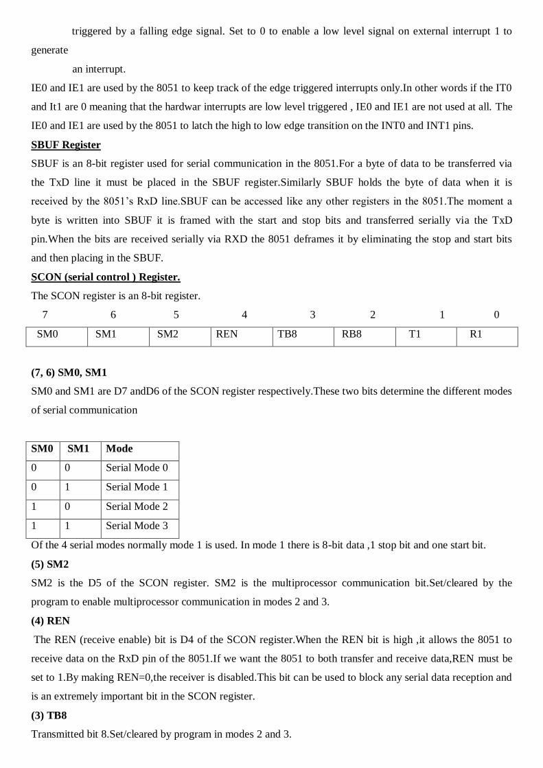
SCON (serial control ) Register.
The SCON register is an 8-bit register.
7 6 5 4 3 2 1 0
SM0 SM1 SM2 REN TB8 RB8 T1 R1
(7, 6) SM0, SM1
SM0 and SM1 are D7 andD6 of the SCON register respectively.These two bits determine the different modes
of serial communication
SM0 SM1 Mode
0 0 Serial Mode 0
0 1 Serial Mode 1
1 0 Serial Mode 2
1 1 Serial Mode 3
Of the 4 serial modes normally mode 1 is used. In mode 1 there is 8-bit data ,1 stop bit and one start bit.
(5) SM2
SM2 is the D5 of the SCON register. SM2 is the multiprocessor communication bit.Set/cleared by the
program to enable multiprocessor communication in modes 2 and 3.
(4) REN
The REN (receive enable) bit is D4 of the SCON register.When the REN bit is high ,it allows the 8051 to
receive data on the RxD pin of the 8051.If we want the 8051 to both transfer and receive data,REN must be
set to 1.By making REN=0,the receiver is disabled.This bit can be used to block any serial data reception and
is an extremely important bit in the SCON register.
(3) TB8
Transmitted bit 8.Set/cleared by program in modes 2 and 3.
(2) RB8
Received bit 8. Bit 8 of received data in modes 2 and 3
(1, 0) TI ,RI (Serial data interrupts)
TI (transmit interrupt) is bit D1 of the SCON register.This is an extremely important flag in the SCON
register.When the 8051 finishes the transfer of the 8-bit character it raises the TI flag to indicate that it is
ready to transfer another byte.The TI flag is raised at the beginning of the stop bit.
RI (receive interrupt) is the D0 bit of the SCON register.This is also an important flag bit in the SCON
register.When the 8051 receives data serially via RxD it, the data is placed in the SBUF register.Then it
raises the RI flag to indicate that a byte has been received and should be picked up before it is lost.RI is
raised half way through the stop bit.
Power mode control (PCON) Register
7 6 5 4 3 2 1 0
SMOD ----- ----- ----- GF1 GF0 PD IDL
(7) SMOD – Serial baud rate modify bit.Set to 1 by program to double baud rate using timer 1.Cleared to 0 to
use timer 1 baud rate.
(6,5,4) --- Not implemented
(3) GF1 – General purpose user flag bit 1
(2) GF0 – General purpose user flag bit 0
(1) PD – Power down bit.
(0) IDL – Idle mode bit.
Instruction Syntax of 8051
An Assembly instruction consists of four fields.
[ label:] mnemonic [operands] [; comment]
The label field allows the program to refer to a line of code by name. The label field cannot exceed a certain
number of characters. Any label referring to an instruction must be followed by a colon symbol.
The assembly language mnemonic (instruction) and operands fields together perform the real work of the
program and accomplish the tasks for which the program was written. In assembly language program such as
ADD A, B
8051 Instruction Set
The instruction sets in 8051 are classified as
1. Data transfer instructions
2. Jump and Call instructions
3. Single bit instructions
4. Logic instructions
5. Arithmetic instructions
Data transfer instructions
The data transfer instructions may be divided into the following three main types
1. MOV destination, source
2. PUSH source or POP destination
3. XCH destination, source
MOV
A data MOV does not alter the contents of the data source address. A copy of the data is made from the
source and moved to the destination address. The contents of the destination address are replaced by the
source address contents.
Eg:- MOV 56H, A ; save content of A in RAM location 56H
MOV A, R0 ; copy the contents of R0 into A
MOV R0, 40H ; save content of RAM location 40H in R0.
An X is added to the MOV mnemonics to serve as a reminder that the data move is external to the
8051.MOVX can be used only with register indirect addressing mode.
Eg:- MOVX A, @R1 ; copy the contents of the external address in R1 to A
MOVX @R0, A ; copy data from A to the 8-bit address in R0
The letter C is added to the MOV mnemonics to highlight the use of the opcodes for moving data from the
source address to the code ROM to the A register in 8051
Eg:- MOVC A, @A+DPTR ; copy the code byte found at the ROM address formed by adding A and
the
DPTR to A
PUSH and POP
PUSH opcode copies data from the source address to the stack. Stack pointer (SP) is incremented by 1
before the data is copied to the internal RAM location contained in SP.
Eg:- PUSH R3 ; push R3 of bank 0 onto stack
POP opcode copies data from the stack to the destination address. SP is decremented by 1 after data is
copied from the stack RAM address to the direct destination.
Eg:- POP R4 ; pop the stack top into R4 of bank 0
XCH
XCH instruction moves data in two directions; from source to destination and from destination to source.
XCH instruction exchanges the contents of destination and source.
Eg:- XCH A,R7 ; exchange byte between register A and register R7
XCH A, 0F0H ; exchange byte between register A and register B
XCHD exchanges lower nibbles of destination and source.While using XCHD the upper nibble of destination
and source do not change.
Eg:- XCHD A, @R1 ; exchange lower nibbles in, A and address in R1
Jump and Call instructions
Conditional Jump Instructions
DJNZ
The syntax is “DJNZ reg , label” . In this instruction the register is decremented ; if it is not zero, it jumps to
the target address referred to by the label. In this instruction both the register decrement and the decision to
jump are combined into a single instruction.
Eg:- MOV R2, #09H
AGAIN: ADD A, #03H
DJNZ R2, AGAIN ; Decrement R2 by 1 and jump to “AGAIN” if R@ is not zero
JZ ( jump if A = 0 )
In this instruction the content of register A is checked.If it is zero it jumps to the target address.
Eg:- MOV A, R0
JZ OVER
MOV A, R1 ; jump if A = 0
OVER: MOV A,R2
JNC ( jump if no carry, jump if CY = 0 )
In executing “JNC label” the processor looks at the carry flag to see if it is raised (CY = 1). If it is not the
CPU starts to fetch and execute instructions from the address of the label. If CY = 1it will not jump but will
execute the next instruction below JNC.
ADD A, #79H
JNC LOOP ; jump if CY = 0
INC R5
LOOP: ADD A, #0F5H
JC ( jump if carry, jump if CY = 1 )
In the JC instruction if CY = 1 it jumps to the target address
ADD A, #79H
JC LOOP ; jump if CY = 1
INC R5
LOOP: ADD A, #0F5H
8051 Conditional Jump Instructions
Instruction Action
JZ Jump if A = 0
JNZ Jump if A not equal to 0
DJNZ Decrement and jump if A not equal to zero
CJNE A, byte Compare and jump if A not equal to byte
CJNE reg, #data Compare and jump if byte not equal to #data
JC Jump if CY = 1
JNC Jump if CY = 0
JB Jump if bit = 1
JNB Jump if bit = 1
JBC Jump if bit = 1 and clear bit
Unconditional Jump Instructions
LJMP (long jump)
LJMP is an unconditional long jump.It is a 3-byte instruction in which the first byte is the opcode and the
second and third byte represent the 16-bit address of the target location.The 2-byte target address allows a
jump to any memory location from 0000 to FFFFH.
SJMP (short jump)
In this 2-byte instruction the first byte is the opcode and the second byte is the relative address of the target
location. The relative address range is from 00 to FFH.
CALL Instructions
Call instructions are always used to call subroutines. In the 8051 there are two instructions for call:
LCALL (long call) and ACALL (absolute call).
LCALL (long call)
It is a 3-byte instruction in which the first byte is the opcode and the second and third byte represent the
address of the target subroutine. Therefore LCALL can be used to call subroutines located anywhere within
64Kbyte address space of the 8051.
ACALL (absolute call)
ACALL is a 2-byte instruction in contrast to LCALL which is 3 bytes.Since ACALL is a 2-byte instruction
the target address of the subroutine must be within 2K bytes address.
Single bit instructions
Instructions that are used for single bit operations are called single bit instructions.
SETB bit
Set the bit ie, bit = 1
Eg:- SETB P1.0 ; Bit 0 of port 1 is set to high
CLR bit
Clear the bit ie, bit = =0
Eg:- CLR P1.0 ; Bit 0 of port 1 is cleared
CPL bit
Complement the bit
Eg:- CPL P1.3 ; complement bit 3 of port 1
Other single bit instructions are JB. JNB, JBC etc.
Logic instructions
ANL
The syntax is ANL destination , source
This instruction will perform a logical AND on the two operands and place the result in the destination. The
destination is normally the accumulator. The source operand can be a register, in memory or immediate. The
ANL instruction has no effect on any of the flags.
Eg:- MOV A, #35H
ANL A, #0FH ; A= A AND 0FH = 05H
ORL
The syntax is ORL destination , source
This instruction will perform a logical OR on the two operands and place the result in the destination. The
destination is normally the accumulator. The source operand can be a register, in memory or immediate. The
ORL instruction has no effect on any of the flags.
Eg:- MOV A, #04H
ORL A, #68H ; A= 6CH
XRL
The syntax is XRL destination , source
This instruction will perform a logical OR on the two operands and place the result in the destination. The
destination is normally the accumulator. The source operand can be a register, in memory or immediate. The
XRL instruction has no effect on any of the flags.
Eg:- MOV A, #54H
XRL A, #78H ; A= 2CH
CPL A (complement accumulator)
This instruction complements the contents of register A. The complement action changes the 0s to 1s and
the 1s to 0s.
Eg:- MOV a, #55H
CPL A now ; A = AAH 0101 0101 (55H) becomes 1010 1010 (AAH)
CJNE
The syntax is CJNE destination , source
The CJNE instruction compares two operands and jumps if they are not equal.In addition it changes the carry
flag to indicate if the destination operand is larger or smaller. If destination > source then CY = 0. If
destination < source then CY = 1.In CJNE the destination operand can be in the accumulator or in one of the
Rn registers. The source operand can be a register, in memory or immediate.
Eg:- MOV A ,# 55H
CJNE A,#99H, HERE ; jump to ‘HERE’ because 55H and 99H are not equal
RR (Rotate right A)
The syntax is RR A. In rotate right the 8 bits of the accumulator are rotated right one bit and bit D0 exits
from the least significant bit and enters into D7 (most significant bit).
Eg:- MOV A, #36H ; A = 0011 0110
RR A ; A = 0001 1011
RL (Rotate left A)
The syntax is RR A. In rotate left the 8 bits of the accumulator are rotated left one bit and bit D7 exits from
the MSB and enters into D0.
Eg:- MOV A, #72H ; A = 0111 0010
RL A ; A = 1110 0100
RRC (Rotate right through carry)
The syntax is RRC A. In RRC A the LSB is moved to CY and CY is moved to the MSB.
Eg:- CLR C
MOV A, #26H ; A = 0010 0110
RRC A ; A = 0001 0011 CY = 0
RRC A ; A = 0000 1001 CY = 1
RLC (Rotate left through carry)
The syntax is RLC A. In RLC A the MSB is moved to the carry flag and CY (carry flag) is moved to the
LSB.
Eg:- SETB C
MOV A, #15H ; A = 0001 0101
RLC A ; A = 0010 1011 CY = 0
RLC A ; A = 0101 0110 CY = 0
SWAP
It works only on the accumulator. It swaps the lower nibble and the higher nibble.
Eg:- MOV A, #72H
SWAP A ; A = 27H
Arithmetic instructions
ADD
In the 8051 in order to add numbers together the accumulator register ,A must be involved.The form of the
ADD instruction is
ADD A, source ; A = A + source
The destination operand is always in register A while the source operand can be a register, immediate data or
in memory. The instruction could change any of the AF, CF or PF bits of the flag register, depending on the
operands involved.
Eg:- MOV A, #0F5H
ADD a, #0BH ; A = F5 + 0B = 00
ADDC
The instruction ADDC is used when adding two 16-bit data operands where there is propogation of carry
from the lower byte to the higher byte. The syntax is ADDC a, source.
Eg:- MOV A,#0E7H
ADD A,#8DH ; A = 8DH + E7H = 74H CY = 1
MOV A, #3CH
ADDC A, #3BH ; add with the carry , A = 3BH+3CH+1 = 78H
DA (decimal adjust for addition)
Adding two BCD numbers must give a BCD number. The DA instruction in the 8051 is provided to correct
the problem associated with BCD addition.The mnemonic “DA” has its only operand the accumulator A. The
DA instruction will add 6 to the lower nibble or higher nibble if needed, otherwise it will leave the result
alone.The works only after an ADD instruction.
Eg:- MOV A, #47H
MOV B, #25H
ADD A, B ; A = 6CH
DA A ; adjust for BCD addition ( A = 72H) ;
SUBB (subtract with borrow)
The syntax is SUBB A, source ; A = A - source
8051 executes the SUBB instruction for unsigned numbers as follows.
1. Take the 2’s complement of the subtrahend (source operand)
2. Add it to the minuend. (accumulator)
3. Invert the carry
If after the execution of SUBB the CY = 0 the result is positive, if the CY = 1 the result is negative and the
destination has the 2’s complement of the result.
Eg:- MOV A, #4CH
SUBB A, #6EH ; A = 4C – 6E
MUL
The syntax is MUL AB. MUL is used for byte by byte multiplication. One of the operands must be in
register A, and the second operand must be in register B. After multiplication the result is in the A and B
registers. ; the lower byte is in A and the upper byte is in B.
Eg:- MOV A, #25H
MOV B, #65H
MUL AB ; 25H * 65H = E99H where B = 0EH and A = 99H
DIV
DIV instruction is used for byte over byte division. The syntax is DIV AB ; Divide A by B. The numerator
must be in register A and the denominator must be in B.After the DIV instruction is performed the quotient
is in
A and the remainder is in B.The instruction always makes CY = 0 and OV = 0 if the denominator is not
zero.If
the denominator is 0 OV = 1 indicates an error and CY = 0.
Eg:- MOV A, #95H
MOV B, #10H
DIV AB ; now A = 09H (quotient) and B= 05H (remainder)
8051 Addressing Modes.
The CPU can access data in various ways.The data could be in a register ,or in memory or be provided as an
immediate value.These various ways of accessing data are called addressing modes.The 8051 provides a total
of five addressing modes. They are
1. Immediate addressing mode
2. Register addressing mode
3. Direct addressing mode
4. Register indirect addressing mode
5. Indexed addressing mode
Immediate addressing mode
In this addressing mode the source operand is a constant. In immediate addressing mode as the name
implies the operand comes immediately after the opcode. Notice that the immediate data must be preceded by
the pound sign, “ # ” .This addressing mode can be used to load information into any of the registers,
including the DPTR register.
Eg:- MOV A, #25H ; load 25H into A
MOV B, #40H ; load 40H into B
MOV DPTR, #4521H ; load 4512H into DPTR
MOV R4, #62H ; load 62H into R4
Register addressing mode
Register addressing mode involves the use of registers to hold the data to be manipulated. It should be
noted that the source and destination registers must match in size. In other words , coding “ MOV DPTR , A”
will give an error, since the source is an 8- bit register and the destination is a 16-bit register. Also notice that
we can move data between the accumulator and Rn(for n = 0 to 7) but movement of data between Rn
registers is not allowed.
Eg:- MOV A, R0 ; copy the contents of R0 into A
MOV R2, A ; copy the contents A into R2
MOV R6, A ; copy the contents A into R6
ADD A, R7 ; add the contents of R7 to contents of A
Direct addressing mode
In direct addressing mode , the data is in a RAM memory location whose address is known and this
address is
given as a part of the instruction. The “ # “ sign distinguishes between the immediate and direct addressing
modes. Another major use of direct addressing mode is the stack. In 8051 only direct addressing mode is
allowed for pushing onto the stack. Direct addressing mode must be used for the POP instruction as well.
There for an instruction such as ‘PUSH A’ is invalid. Pushing the accumulator onto the stack is coded as
‘PUSH 0E0H’ where 0E0 is the address of register A. The SFRs can be accessed by their names or by their
addresses.
Eg:- MOV R0, 40H ; save content of RAM location 40H in R0.
MOV 56H, A ; save content of A in RAM location 56H
PUSH R3 ; push R3 of bank 0 onto stack
POP R4 ; pop the stack top into R4 of bank 0
MOV B, # 25H ; is the same as
MOV 0F0H, # 25H ; which means load 25H into B
Register indirect addressing mode
In the register indirect addressing mode a register is used as a pointer to the data.If the data is inside the
CPU only registers R0 and R1 are used for this purpose.In other words R2- R7 cannot be used to hold the
address of an operand located in RAM when using this addressing mode.When R0 and R1 are used they must
be preceded by the “@” sign.One of the advantage of register indirect addressing mode is that looping can
be done by using this addressing mode.Looping is not possible in direct addressing mode.This the main
difference between the direct and register indirect addressing modes.
Eg:- Mov A, @R0 ; move contents of RAM location whose address is held by R0 into A
MOV @R1, B ; move contents of B into RAM location whose address is held by R1
KEIL C
The use of C language to program microcontrollers is becoming too common. And most of the time its not easy to buld
an application in assembly which instead you can make easily in C. So its important that you know C language for
microcontroller which is commonly known as Embedded C. As we are going to use Keil C51 Compiler, hence we also
call it Keil C.
Some keywords associated with Keil C programming are
data/idata
Description: The variable will be stored in internal data memory of controller
bdata
Description: The variable will be stored in bit addressable memory of controller.
xdata
Description: The variable will be stored in external RAM memory of controller
Code
Description: This keyword is used to store a constant variable in code memory
pdata
Description: This keyword will store the variable in paged data memory
_at_
Description: This keyword is used to store a variable on a defined location in ram
sbit
Description: This keyword is used to define a special bit from SFR (special function register) memory.
Sfr
Description: sfr is used to define an 8-bit special function register from sfr memory.
using
Description: This keyword is used to define register bank for a function. User can specify register bank 0 to 3
interrupt
Description: This keyword will tells the compiler that function described is an interrupt service routine. C51 compiler
supports interrupt functions for 32 interrupts (0-31).
Memory Models
There are three kind of memory models available for the user:
Small
All variables in internal data memory.
Compact
Variables in one page, maximum 256 variables (limited due to addressing scheme, memory accessed indirectly using r0
and r1 registers);
Large
All variables in external ram. variables are accessed using DPTR.
Pointers in Keil C
Pointers in keil C is are similar to that of standard C and can perform all the operations that are available in standard C.
In addition, keil C extends the operatability of pointers to match with the 8051 Controller architecture. Keil C provides two different types of pointers:
Generic Pointers
Memory-Specific Pointers
Example program
Generate a square wave of 2 KHz frequency at pin P1.0 of 8051 using timer 0
#include <reg51.h> // include 8051 register file
sbit pin = P1^0; // decleare a variable type sbit for P1.0
main()
{
P1 = 0x00; // clear port
TMOD = 0x09; // initialize timer 0 as 16 bit timer
loop:TL0 = 0x1A; // load valur 15535 = 3CAFh so after
TH0 = 0xFF; // 50000 counts timer 0 will be overflow
pin = 1; // send high logic to P1.0
TR0 = 1; // start timer
while(TF0 == 0) {} // Delay
TL0 = 0x1A; // again reload count
TH0 = 0xFF;
pin = 0; // now send 0 to P1.0
while(TF0 == 0) {} // Delay
goto loop; // continue with the loop
}
Buzzer interface with 8051 microcontroller
Buzzer is a electronic device that converts the electronic signal into buzzing noise, that is applied to it. It can
be used as electronic bell or as quiz buzzer in many applications around us. Here, i world like to discuss the
interfacing of a small buzzer with 8051 microcontroller and how different projects can be constructed.
Buzzer Interfacing:
This project shows the interface with AT89S52 microcontroller to a buzzer. When a push button is pressed,
the buzzer will get ON and OFF (number of times set in the code) and then stops.
Circuit Diagram:
The port P1 of the microcontroller is connected to buzzer. This type of connection is possible, if the
current requirements of the buzzer is not more than 20mA. The output is in current source mode so that
buzzer will turn ON when the output of the port is logic LOW. Switch is connected to port P3 which remains
at logic HIGH by pull up resistor.
Code:
#include "REG52.h"
#define buz P1
sbit SW=P3^0;
long int i;
void main()
{
while(1)
{
if (SW==0)
{
for(i=0;i<=90000;i++);
if(SW==0)
{
while(SW==0);
buz=0x01; // ON Buzzer
for(i=0;i<4500;i++); // Delay
buz=0x00; // OFF Buzzer
for(i=0;i<4500;i++); // Delay
} }
} }
According to the code: The buzzer is interfaced to Port P1 of the microcontroller and simple ON/OFF
program is written as an example using delay in between them. For half period, buzzer gets ON automatically
and for next half period, buzzer gets OFF automatically as described in the code. One can also use the switch
concept to control the ON/OFF operation of buzzer. Here, switch is connected to Port P3.0 pin
and Debouncing concept is applied.
EE309Microprocessor and Embedded Systems
Embedded Programming in C, data type and time delay in C, I/O port programming
ICET EEE
24-11-2017ARUN XAVIER, VAST
2
ModuleVI
• 8051- assembly language programming, data
types and directives, Time delay and I/O port programming, Embedded Programming in C, data type and time delay in C, I/O port programming, Timer / counter programming, serial port programming, Interfacing –LCD, Steppermotor, ADC and DAC.
ICET EEE
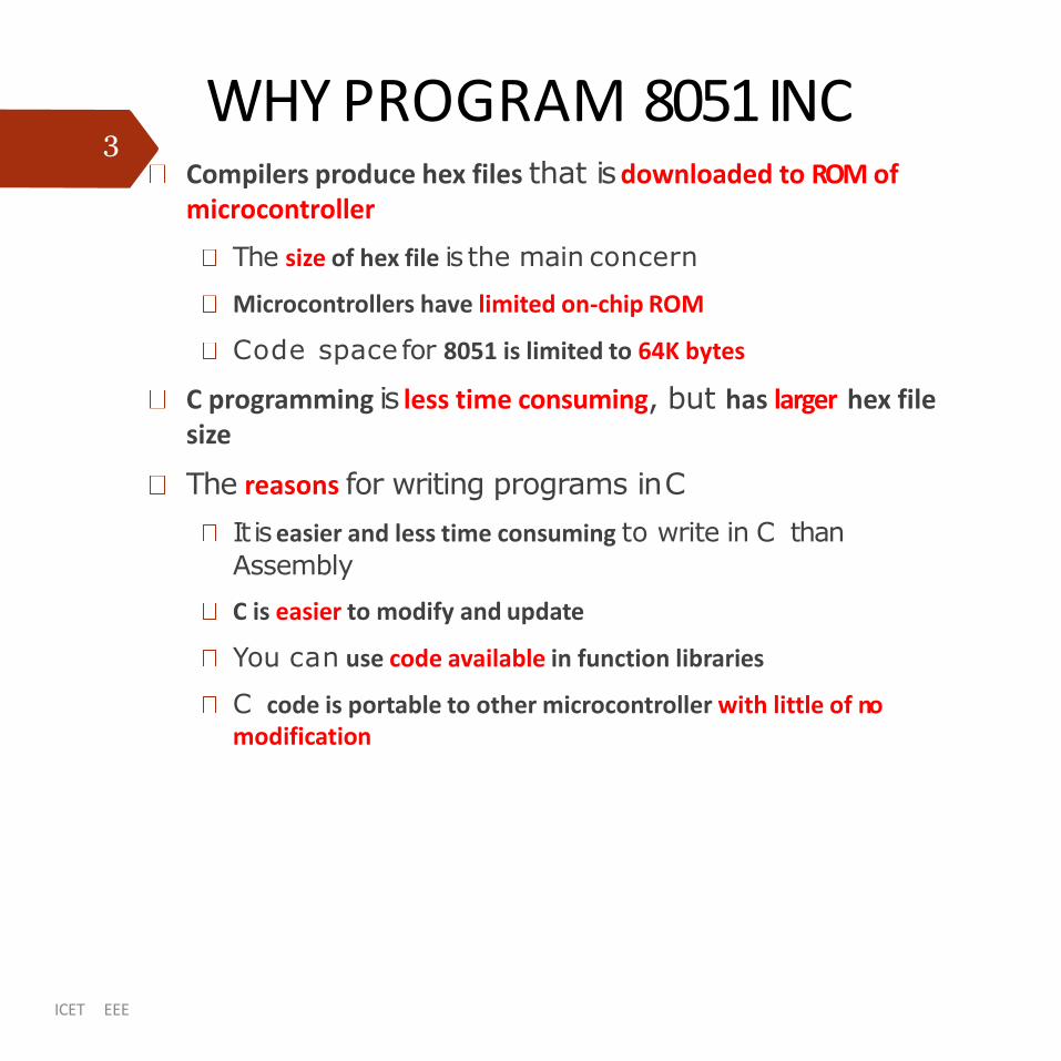
WHY PROGRAM 8051 INC
ICET EEE
Compilers produce hex files that is downloaded to ROM ofmicrocontroller
The size of hex file is the main concern
Microcontrollers have limited on-chip ROM
Code space for 8051 is limited to 64K bytes
C programming is less time consuming, but has larger hex file size
The reasons for writing programs inC
It is easier and less time consuming to write in C than
Assembly
C is easier to modify and update
You can use code available in function libraries
C code is portable to other microcontroller with little of no modification
3
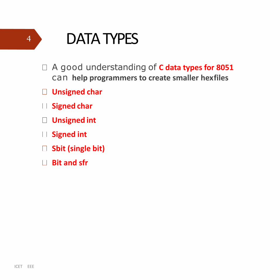
DATA TYPES
ICET EEE
A good understanding of C data types for 8051can help programmers to create smaller hexfiles
Unsigned char
Signed char
Unsigned int
Signed int
Sbit (single bit)
Bit and sfr
4
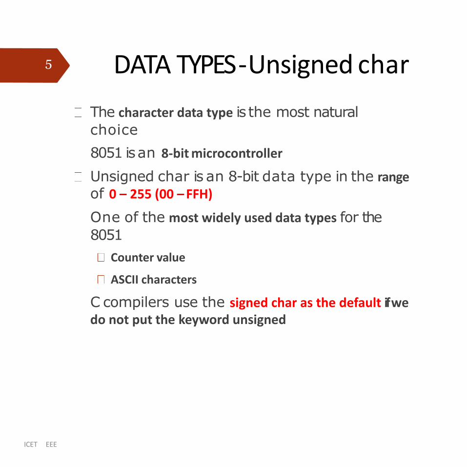
DATA TYPES -Unsigned char
ICET EEE
The character data type is the most natural
choice
8051 is an 8-bit microcontroller
Unsigned char is an 8-bit data type in the rangeof 0 – 255 (00 –FFH)
One of the most widely used data types for the
8051
Counter value
ASCII characters
C compilers use the signed char as the default if we do not put the keyword unsigned
5
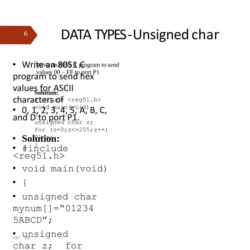
6 DATA TYPES -Unsigned char
• Write an 8051 C program to send hex values for ASCII characters of• 0, 1, 2, 3, 4, 5, A, B, C, and D to port P1.
• Solution:• #include<reg51.h>
• void main(void)
• {
• unsigned char
mynum[]=“01234
5ABCD”;
• unsigned
char z; for
(z=0;z<=10;z+
ICET EEE
Write an 8051 C program to send
values 00 – FF to port P1
Solution:#include <reg51.h>
void main(void)
{
unsigned char z;
for (z=0;z<=255;z++)
P1=z;
}
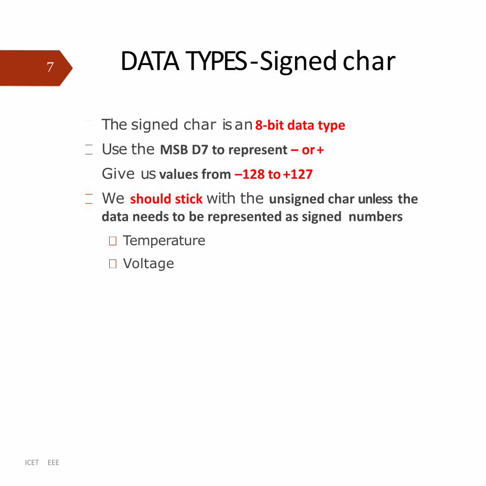
DATA TYPES -Signed char
ICET EEE
The signed char is an8-bit data type
Use the MSB D7 to represent – or+
Give us values from –128 to +127
We should stick with the unsigned char unless the data needs to be represented as signed numbers
Temperature
Voltage
7
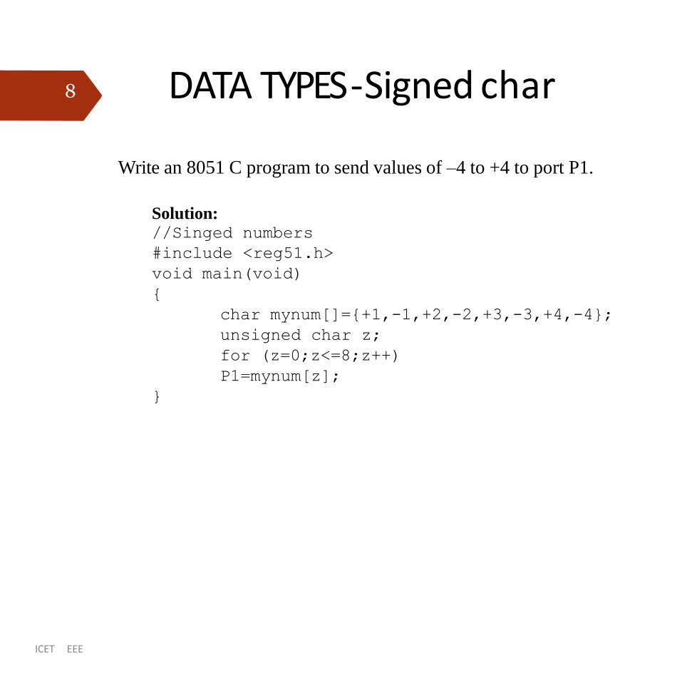
8 DATA TYPES -Signed char
ICET EEE
Write an 8051 C program to send values of –4 to +4 to port P1.
Solution://Singed numbers
#include <reg51.h>
void main(void)
{
char mynum[]={+1,-1,+2,-2,+3,-3,+4,-4};
unsigned char z;
for (z=0;z<=8;z++)
P1=mynum[z];
}
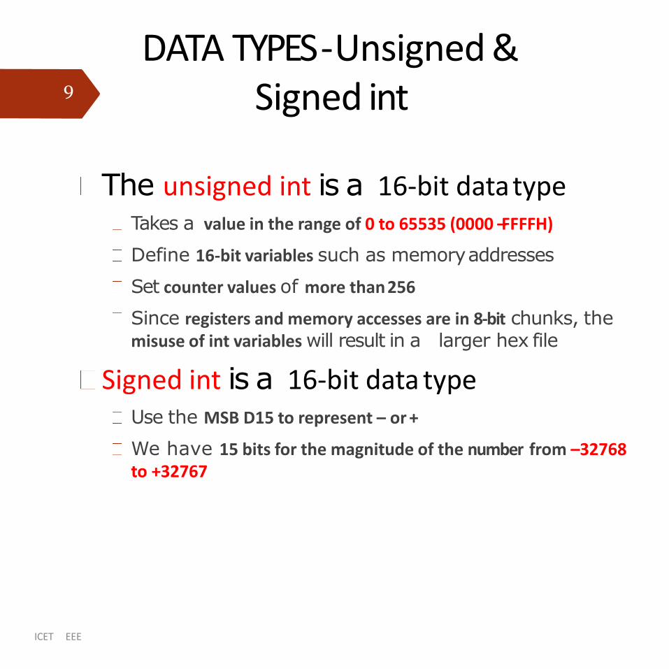
DATA TYPES -Unsigned & Signed int
The unsigned int is a 16-bit datatypeTakes a value in the range of 0 to 65535 (0000 –FFFFH)
Define 16-bit variables such as memoryaddresses
Set counter values of more than256
Since registers and memory accesses are in 8-bit chunks, the misuse of int variables will result in a larger hex file
Signed int is a 16-bit data typeUse the MSB D15 to represent – or +
We have 15 bits for the magnitude of the number from –32768 to +32767
ICET EEE
9
DATA TYPES -SingleBit(Sbit)
ICET EEE
Widely used in 8081 C data type specifically to access single-bit addressable registers
It allows access to thesingle bit of SFR registers
SFR are widely used & also the bit-addressable ports of P0-P3
10
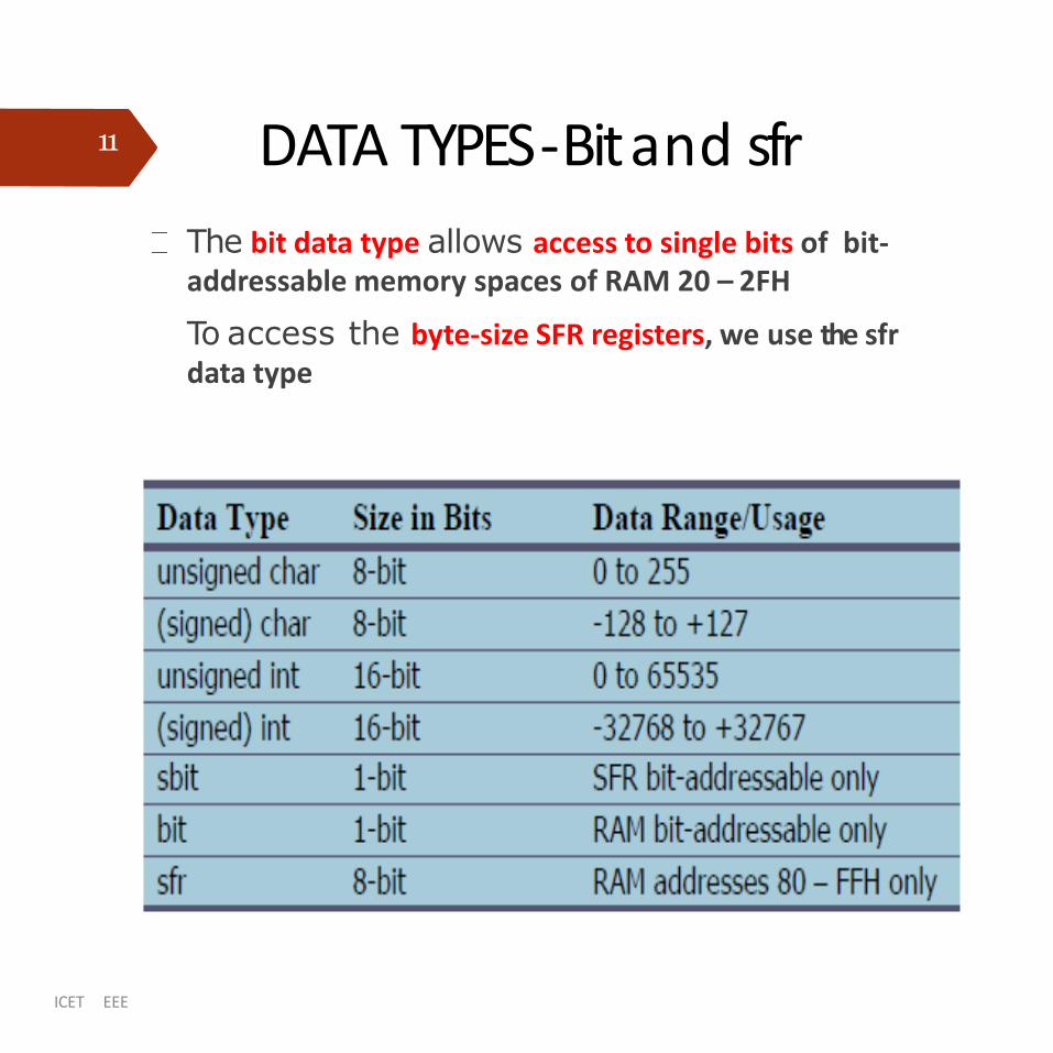
DATA TYPES -Bit and sfr
ICET EEE
The bit data type allows access to single bits of bit-addressable memory spaces of RAM 20 – 2FH
To access the byte-size SFR registers, we use the sfr data type
11
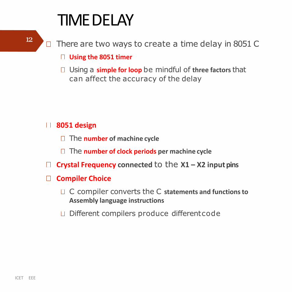
TIMEDELAY
ICET EEE
There are two ways to create a time delay in 8051 C
Using the 8051 timer
Using a simple for loop be mindful of three factors that
can affect the accuracy of the delay
8051 design
The number of machine cycle
The number of clock periods per machine cycle
Crystal Frequency connected to the X1 – X2 input pins
Compiler Choice
C compiler converts the C statements and functions toAssembly language instructions
Different compilers produce differentcode
12
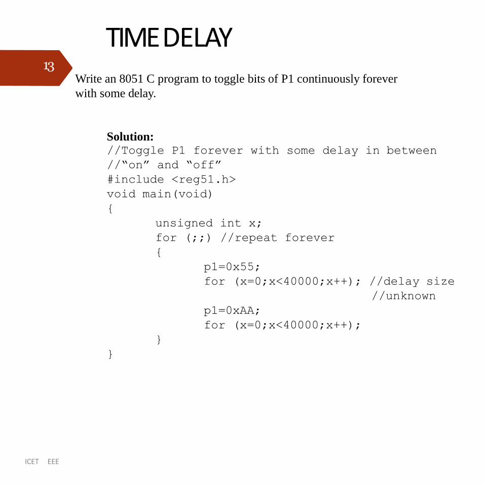
TIMEDELAY
ICET EEE
13Write an 8051 C program to toggle bits of P1 continuously forever
with some delay.
Solution://Toggle P1 forever with some delay in between
//“on” and “off”
#include <reg51.h>
void main(void)
{
unsigned int x;
for (;;) //repeat forever
{
p1=0x55;
for (x=0;x<40000;x++); //delay size
//unknown
p1=0xAA;
for (x=0;x<40000;x++);
}
}
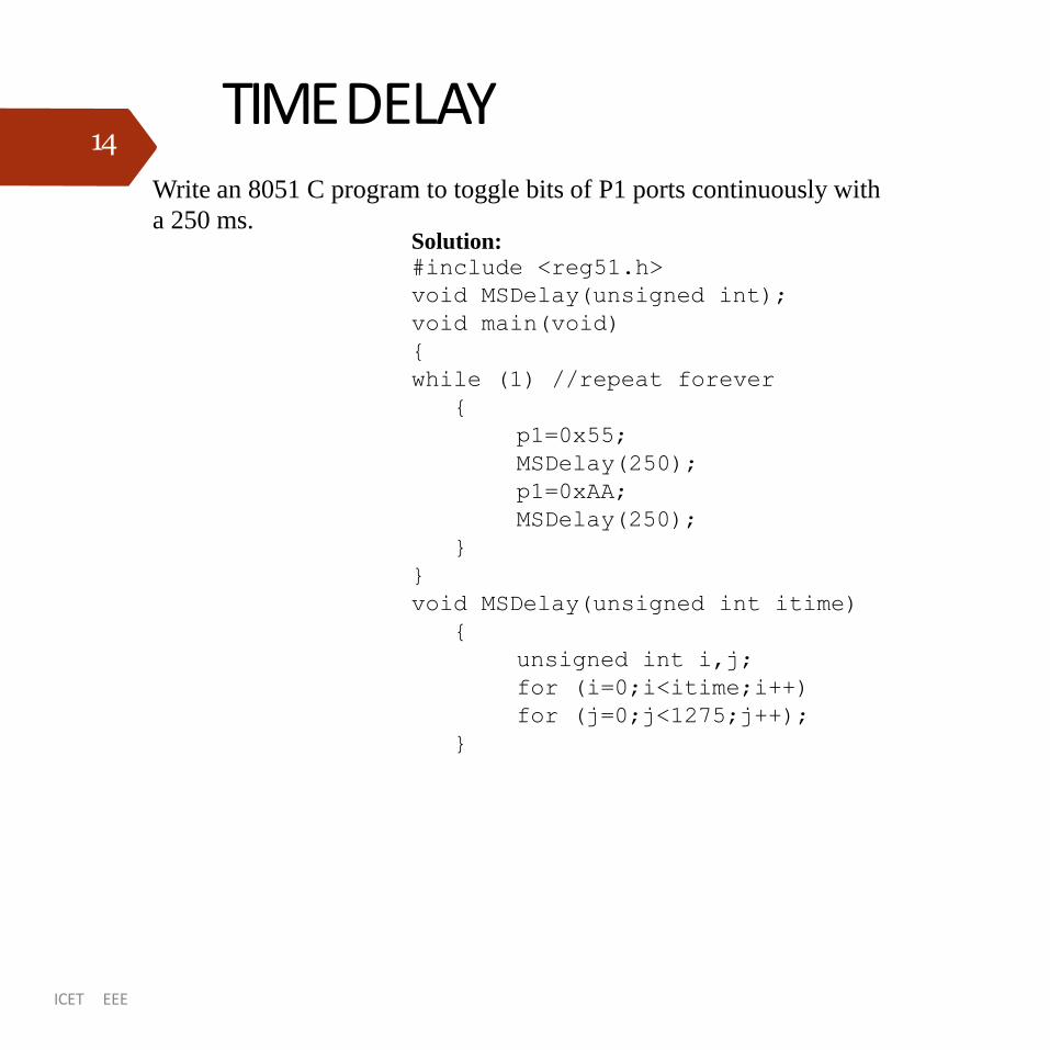
TIMEDELAY
ICET EEE
14
Write an 8051 C program to toggle bits of P1 ports continuously with
a 250 ms.Solution:#include <reg51.h>
void MSDelay(unsigned int);
void main(void)
{
while (1) //repeat forever
{
p1=0x55;
MSDelay(250);
p1=0xAA;
MSDelay(250);
}
}
void MSDelay(unsigned int itime)
{
unsigned int i,j;
for (i=0;i<itime;i++)
for (j=0;j<1275;j++);
}
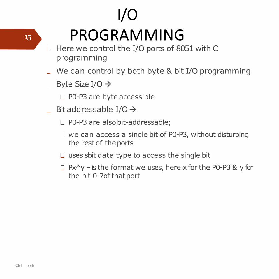
I/OPROGRAMMING
ICET EEE
15
Here we control the I/O ports of 8051 with C programming
We can control by both byte & bit I/O programming
Byte Size I/O→
P0-P3 are byte accessible
Bit addressable I/O→
P0-P3 are alsobit-addressable;
we can access a single bit of P0-P3, without disturbing the rest of theports
uses sbit data type to access the single bit
Px^y – is the format we uses, here x for the P0-P3 & y for the bit 0-7of thatport
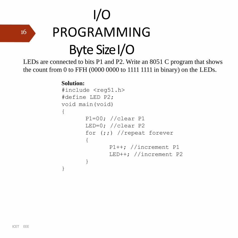
I/OPROGRAMMING
Byte SizeI/O
ICET EEE
16
LEDs are connected to bits P1 and P2. Write an 8051 C program that shows
the count from 0 to FFH (0000 0000 to 1111 1111 in binary) on the LEDs.
Solution:#include <reg51.h>
#define LED P2;
void main(void)
{
P1=00; //clear P1
LED=0; //clear P2
for (;;) //repeat forever
{
P1++; //increment P1
LED++; //increment P2
}
}
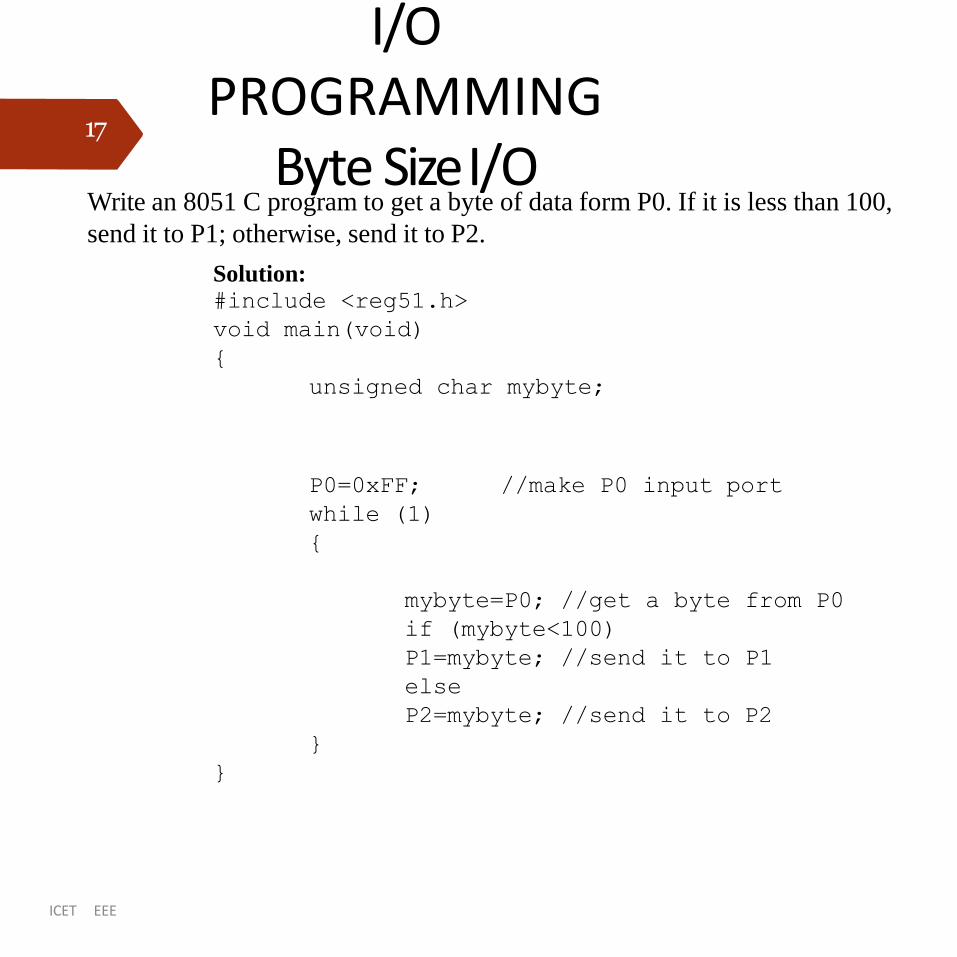
17
I/OPROGRAMMING
Byte SizeI/O
ICET EEE
Write an 8051 C program to get a byte of data form P0. If it is less than 100,
send it to P1; otherwise, send it to P2.
Solution:#include <reg51.h>
void main(void)
{
unsigned char mybyte;
//make P0 input portP0=0xFF;
while (1)
{
mybyte=P0; //get a byte from P0
if (mybyte<100)
P1=mybyte; //send it to P1
else
P2=mybyte; //send it to P2
}
}
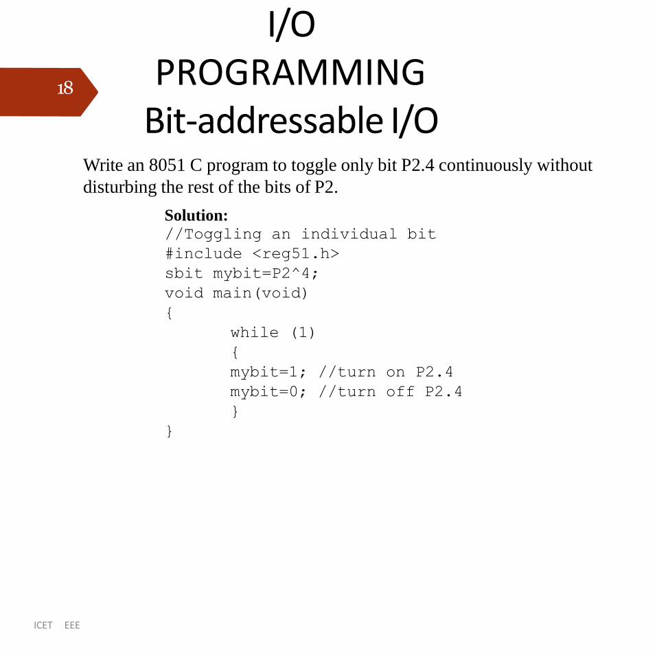
I/OPROGRAMMING
Bit-addressable I/O
ICET EEE
18
Write an 8051 C program to toggle only bit P2.4 continuously without
disturbing the rest of the bits of P2.
Solution://Toggling an individual bit
#include <reg51.h>
sbit mybit=P2^4;
void main(void)
{
while (1)
{
mybit=1; //turn on P2.4
mybit=0; //turn off P2.4
}
}
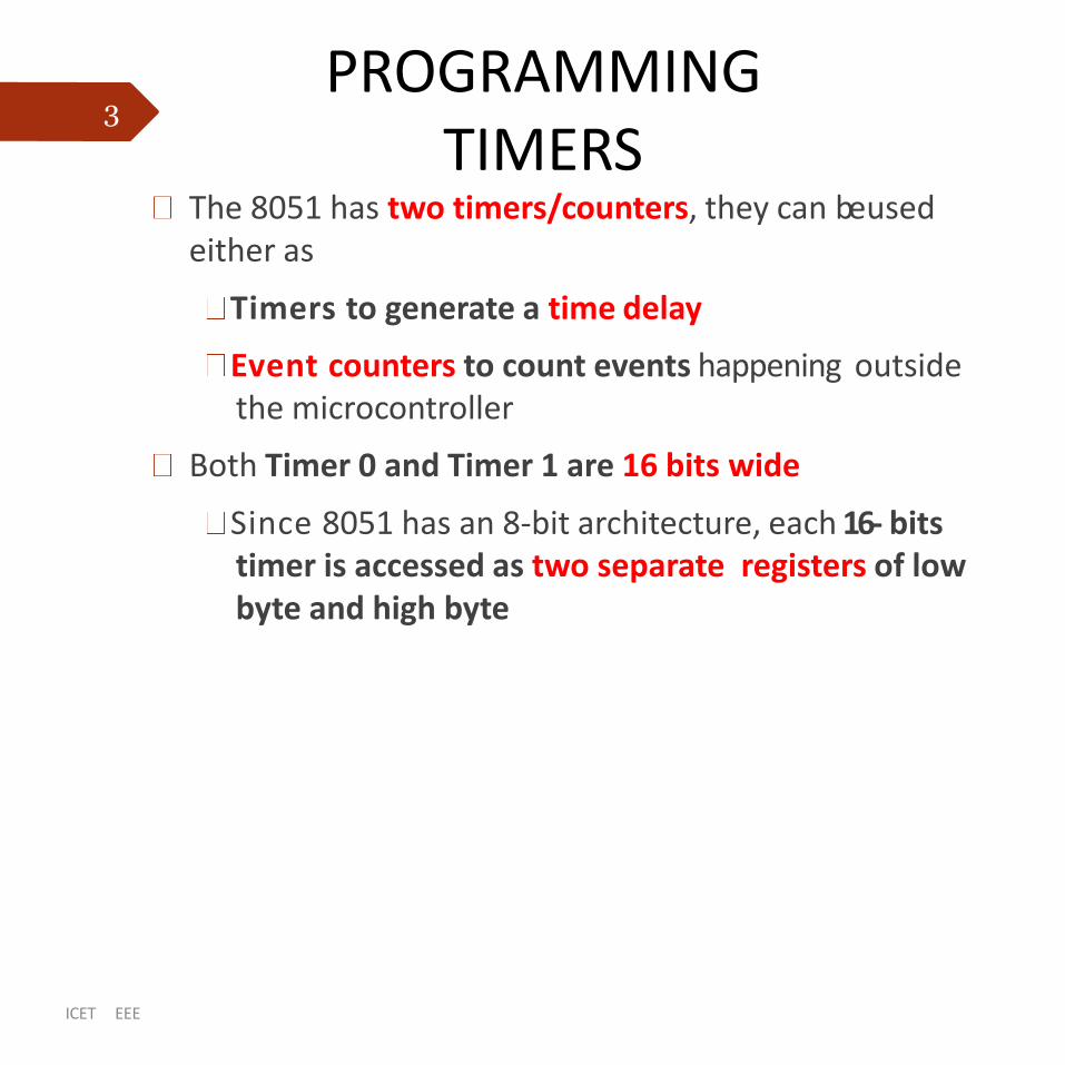
PROGRAMMINGTIMERS
The 8051 has two timers/counters, they can be used either as
Timers to generate a time delay
Event counters to count events happening outside the microcontroller
Both Timer 0 and Timer 1 are 16 bits wide
Since 8051 has an 8-bit architecture, each 16- bits timer is accessed as two separate registers of low byte and high byte
3
ICET EEE
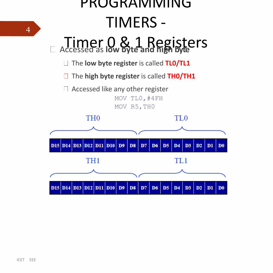
PROGRAMMING TIMERS -
Timer 0 & 1 Registers4
Accessed as low byte and high byte
The low byte register is called TL0/TL1
The high byte register is called TH0/TH1
Accessed like any other registerMOV TL0,#4FH
MOV R5,TH0
ICET EEE
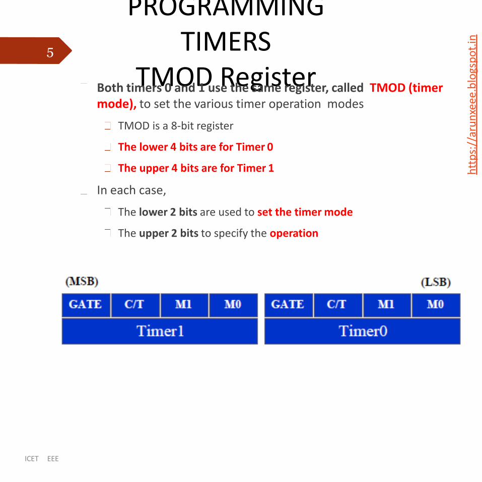
htt
ps:
//ar
un
xeee
.blo
gsp
ot.
in
PROGRAMMINGTIMERS
TMOD Register
ICET EEE
Both timers 0 and 1 use the same register, called TMOD (timer mode), to set the various timer operation modes
TMOD is a 8-bit register
The lower 4 bits are for Timer 0
The upper 4 bits are for Timer 1
In each case,
The lower 2 bits are used to set the timer mode
The upper 2 bits to specify the operation
5
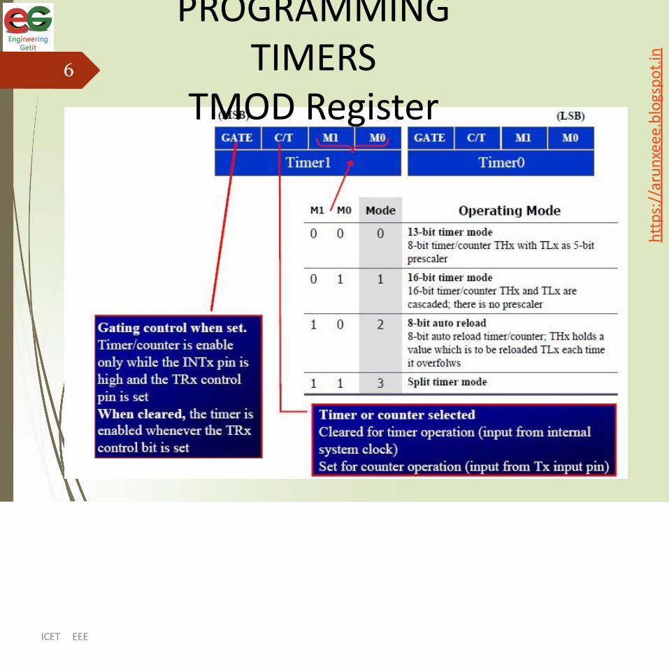
htt
ps:
//ar
un
xeee
.blo
gsp
ot.
in
24-Nov-17ARUN XAVIER VAST
7:27AM
6
PROGRAMMINGTIMERS
TMOD Register
ICET EEE
COUNTERPROGRAMMING
Timers can also be used as counters counting events happening outside the 8051
When it is used as a counter, it is a pulse outside of the 8051 that increments the TH, TL registers
TMOD and TH, TL registers are the same as for the timer discussed previously
Programming the timer in the last section also applies to programming it as a counter
Except the source of the frequency
7
ICET EEE
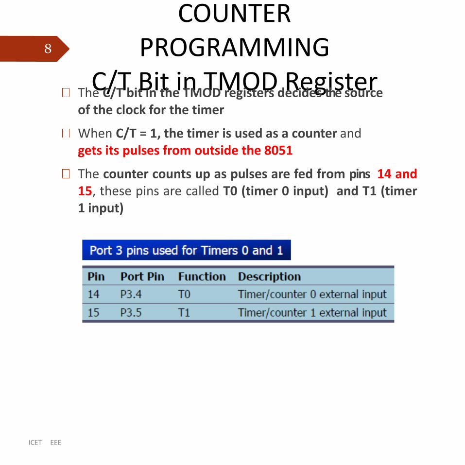
COUNTERPROGRAMMING
C/T Bit in TMOD RegisterThe C/T bit in the TMOD registers decides the source of the clock for the timer
When C/T = 1, the timer is used as a counter andgets its pulses from outside the 8051
The counter counts up as pulses are fed from pins 14 and15, these pins are called T0 (timer 0 input) and T1 (timer1 input)
8
ICET EEE
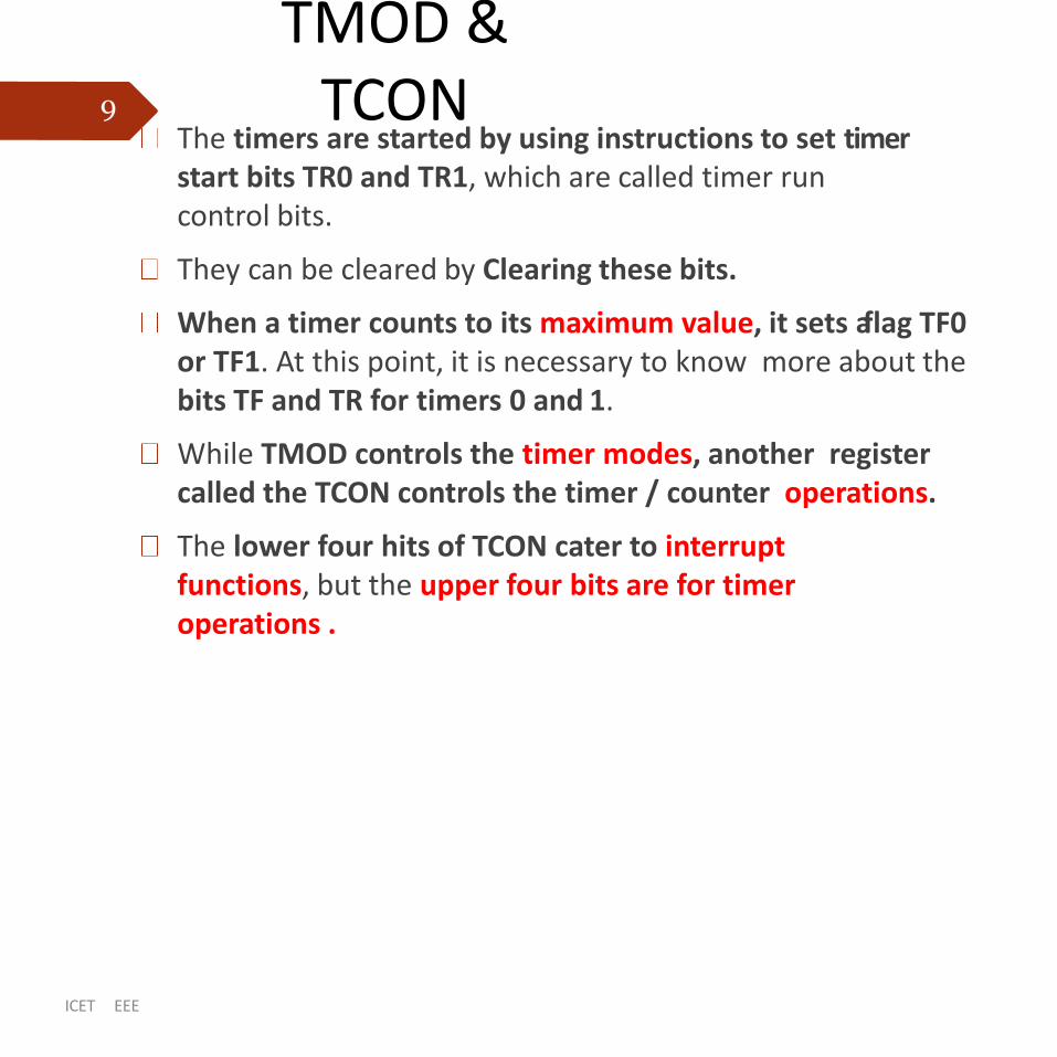
TMOD &TCON9
The timers are started by using instructions to set timerstart bits TR0 and TR1, which are called timer run control bits.
They can be cleared by Clearing these bits.
When a timer counts to its maximum value, it sets a flag TF0 or TF1. At this point, it is necessary to know more about the bits TF and TR for timers 0 and 1.
While TMOD controls the timer modes, another register called the TCON controls the timer / counter operations.
The lower four hits of TCON cater to interrupt functions, but the upper four bits are for timer operations .
ICET EEE
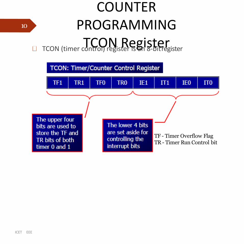
COUNTERPROGRAMMING
TCON RegisterTCON (timer control) register is an 8-bitregister
10
TF - Timer Overflow Flag TR - Timer Run Control bit
ICET EEE
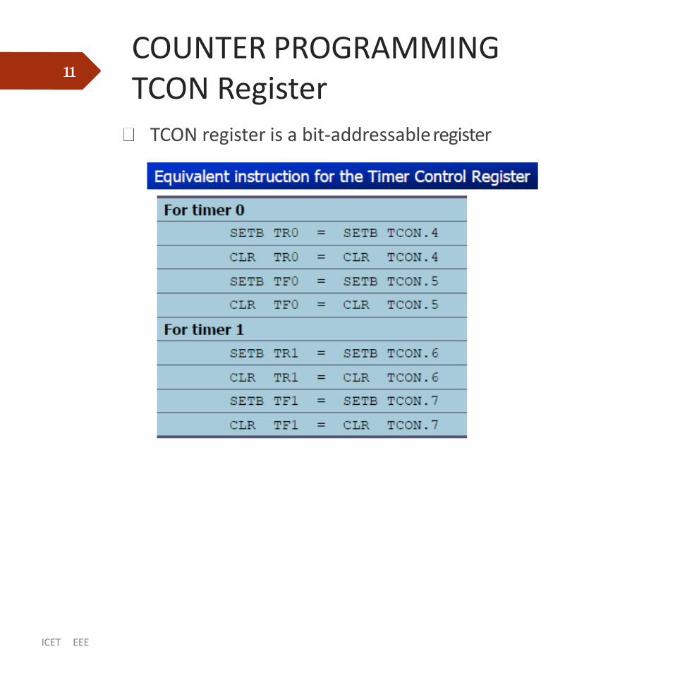
TCON register is a bit-addressableregister
11COUNTER PROGRAMMINGTCON Register
ICET EEE
Calculating Delay
To speed up the 8051, many recent versions of the 8051 have reduced the number of clocks per machine cycle from 12 to four, or even one
The frequency for the timer is always 1/12th thefrequency of the crystal attached to the 8051,regardless of the 8051 version
12
ICET EEE
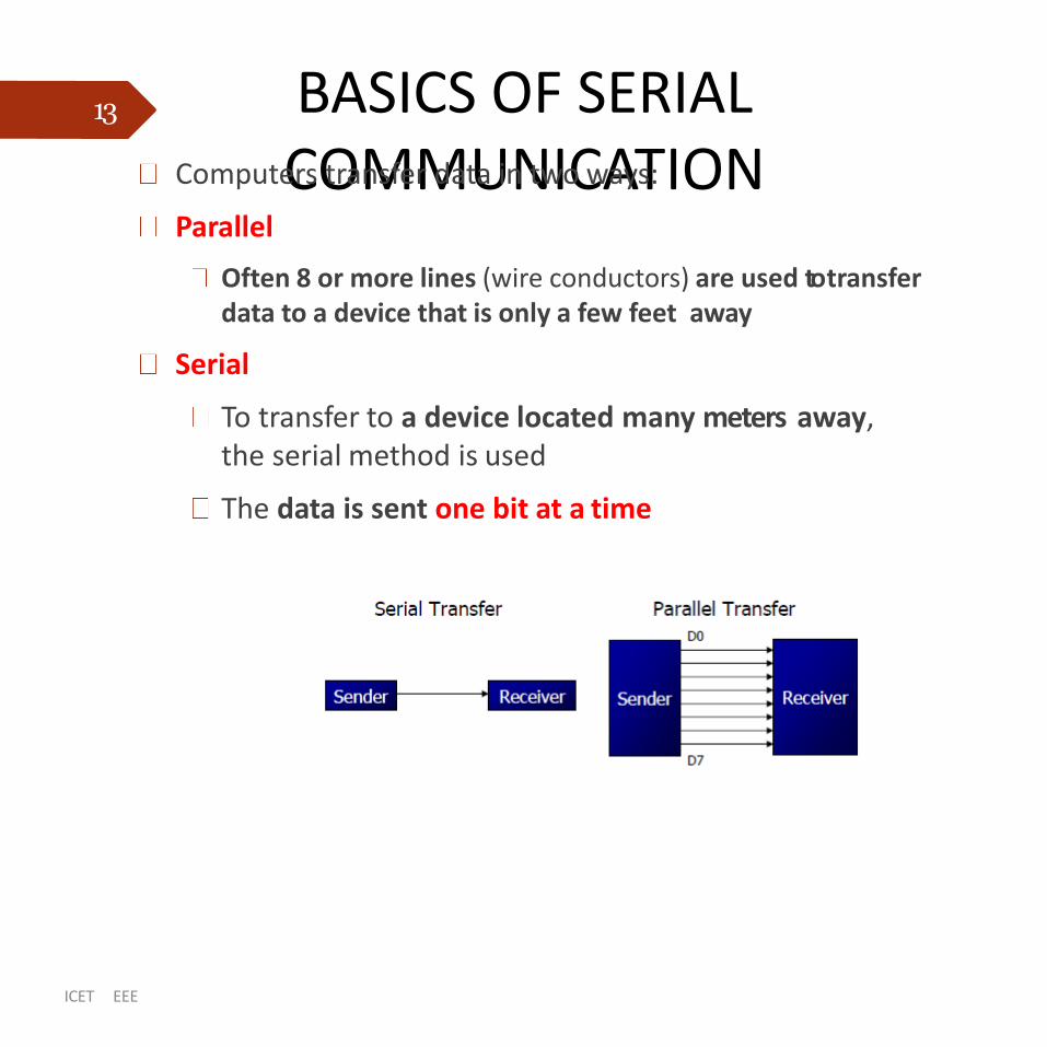
BASICS OF SERIAL COMMUNICATIONComputers transfer data in two ways:
Parallel
Often 8 or more lines (wire conductors) are used to transfer data to a device that is only a few feet away
Serial
To transfer to a device located many meters away, the serial method is used
The data is sent one bit at a time
13
ICET EEE
BASICS OF SERIAL COMMUNICATION
At the transmitting end, the byte of data must be converted to serial bits using parallel-in-serial-out shift register
At the receiving end, there is a serial-in-parallel-out shift register to receive the serial data and pack them into byte
When the distance is short, the digital signal can be transferred as it is on a simple wire and requires no modulation
If data is to be transferred on the telephone line, it must be converted from 0s and 1s to audio tones
ICET EEE
14
Serial data communication uses two methods
Synchronous method transfers a block of data at a time
Asynchronous method transfers a single byte at a time
There are special IC chips made by many manufacturers for serial communications
UART (universal asynchronous Receiver transmitter)
USART (universal synchronous-asynchronous Receiver-transmitter)
BASICS OF SERIAL COMMUNICATION
ICET EEE
15
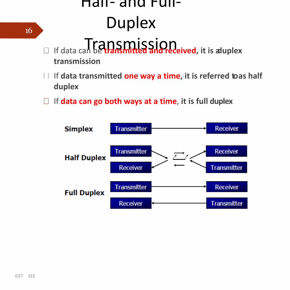
Half- and Full-Duplex
Transmission
ICET EEE
If data can be transmitted and received, it is a duplextransmission
If data transmitted one way a time, it is referred to as halfduplex
If data can go both ways at a time, it is full duplex
16
Start and StopBits
ICET EEE
17
A protocol is a set of rules agreed by both the sender and receiver on
How the data is packed
How many bits constitute a character
When the data begins and ends
Asynchronous serial data communication is widely used for character-oriented transmissions
Each character is placed in between start and stop bits,this is called framing
Block-oriented data transfers use the synchronous method
The start bit is always one bit, but the stop bit can be one or two bits
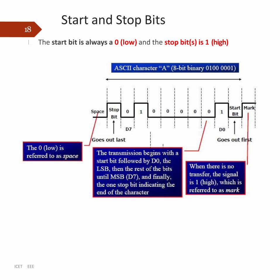
Start and Stop Bits
The start bit is always a 0 (low) and the stop bit(s) is 1 (high)
18
ICET EEE
Start and StopBits
ICET EEE
Due to the extended ASCII characters, 8-bit ASCII data is common
In older systems, ASCII characters were 7-bit
In modern PCs the use of one stop bit is standard
In older systems, due to the slowness of the receiving mechanical device, two stop bits were used to give the device sufficient time to organize itself before transmission of the next byte
19
Data TransferRate
ICET EEE
The rate of data transfer in serial data communication is stated in bps (bits per second)
Another widely used terminology for bps is baud rate
It is modem terminology and is defined as thenumber of signal changes per second
As far as the conductor wire is concerned, the baud rate and bps are the same, and we use the termsinterchangeably
20
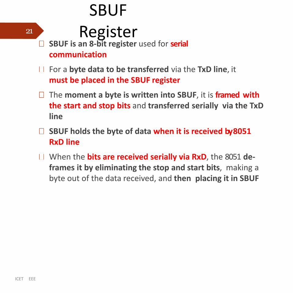
SBUFRegister
ICET EEE
SBUF is an 8-bit register used for serial communication
For a byte data to be transferred via the TxD line, itmust be placed in the SBUF register
The moment a byte is written into SBUF, it is framed with the start and stop bits and transferred serially via the TxDline
SBUF holds the byte of data when it is received by 8051 RxD line
When the bits are received serially via RxD, the 8051 de-frames it by eliminating the stop and start bits, making a byte out of the data received, and then placing it in SBUF
21
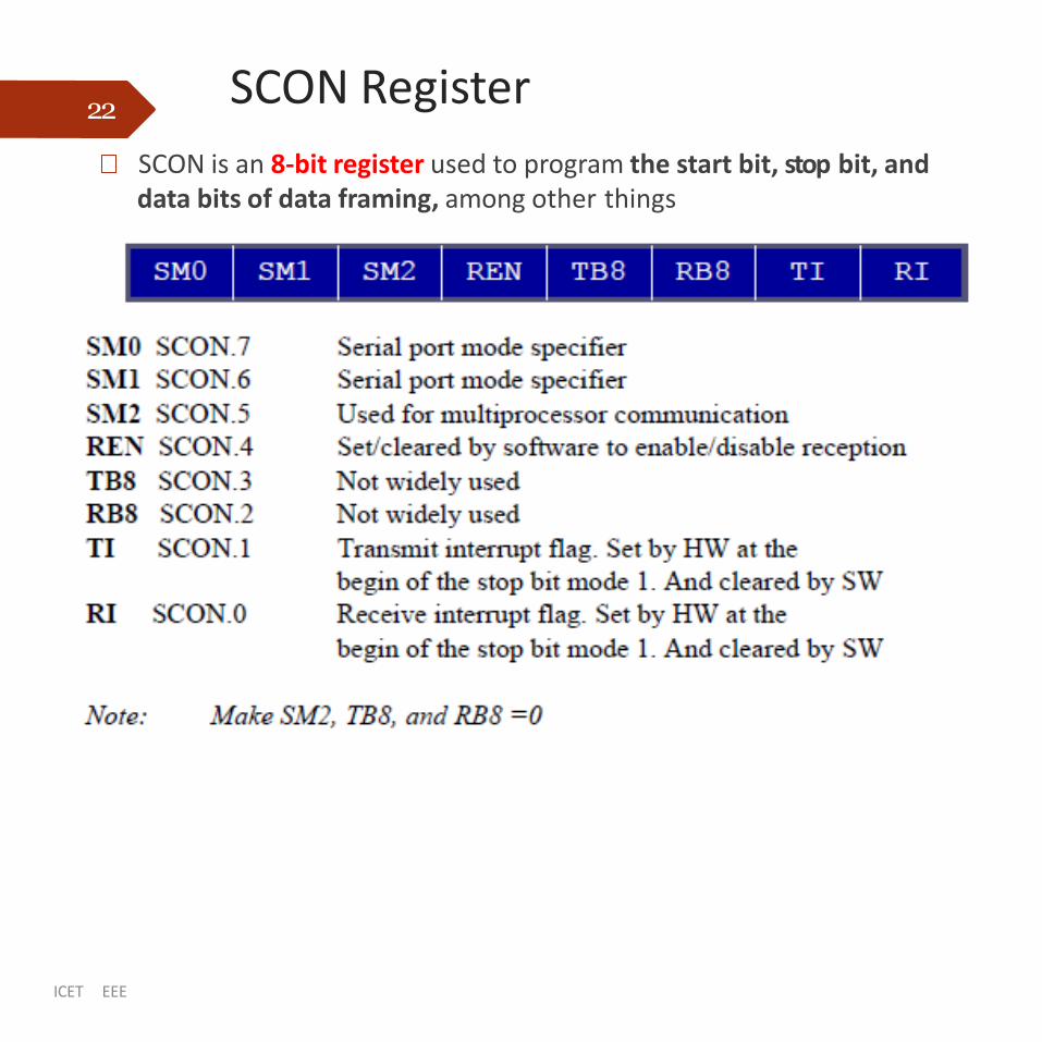
SCON Register
SCON is an 8-bit register used to program the start bit, stop bit, and data bits of data framing, among other things
22
ICET EEE
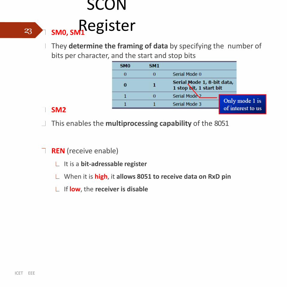
SCONRegister
ICET EEE
SM0, SM1
They determine the framing of data by specifying the number of bits per character, and the start and stop bits
SM2
This enables the multiprocessing capability of the 8051
REN (receive enable)
It is a bit-adressable register
When it is high, it allows 8051 to receive data on RxD pin
If low, the receiver is disable
23
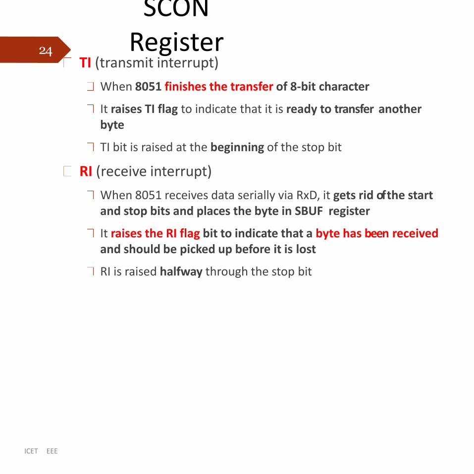
TI (transmit interrupt)
When 8051 finishes the transfer of 8-bit character
It raises TI flag to indicate that it is ready to transfer another byte
TI bit is raised at the beginning of the stop bit
RI (receive interrupt)
When 8051 receives data serially via RxD, it gets rid of the start and stop bits and places the byte in SBUF register
It raises the RI flag bit to indicate that a byte has been received and should be picked up before it is lost
RI is raised halfway through the stop bit
SCONRegister
ICET EEE
24
Programming Serial Data Transmitting
ICET EEE
In programming the 8051 to transfer character bytes serially
1. TMOD register is loaded with the value 20H, indicating the use of timer 1 in mode 2 (8-bit auto-reload) to set baud rate
2. The TH1 is loaded with one of the values to set baud rate for serial data transfer
3. The SCON register is loaded with the value 50H, indicating serial mode 1, where an 8-bit data is framed with start and stop bits
4. TR1 is set to 1 to start timer 1
5. TI is cleared by CLR TI instruction
6. The character byte to be transferred serially is written into SBUF register
7. The TI flag bit is monitored with the use of instruction JNB TI, xx to see if the character has been transferred completely
8. To transfer the next byte, go to step 5
25
Programming Serial Data Transmitting
ICET EEE
26
Write a program for the 8051 to transfer letter “A” serially at 4800
baud, continuously.
Solution:MOV TMOD,#20H
MOV TH1,#-6
MOV SCON,#50H
SETB TR1
AGAIN: MOV SBUF,#”A”
HERE: JNB TI,HERE
CLR TI
SJMP AGAIN
;timer 1,mode 2(auto reload)
;4800 baud rate
;8-bit, 1 stop, REN enabled
;start timer 1
;letter “A” to transfer
;wait for the last bit
;clear TI for next char
;keep sending A
Programming Serial Data Receiving
ICET EEE
In programming the 8051 to receive character bytes serially
1. TMOD register is loaded with the value 20H, indicating the use of timer 1 in mode 2 (8-bit auto-reload) to set baud rate
2. TH1 is loaded to set baud rate
3. The SCON register is loaded with the value 50H, indicating serial mode 1, where an 8-bit data is framed with start and stop bits
4. TR1 is set to 1 to start timer 1
5. RI is cleared by CLR RI instruction
6. The RI flag bit is monitored with the use of instruction JNB RI, xx to see if an entire character has been received yet
7. When RI is raised, SBUF has the byte, its contents are moved into a safe place
8. To receive the next character, go to step 5
27
Programming Serial Data Receiving
ICET EEE
28
Write a program for the 8051 to receive bytes of data serially, and put them in P1, set
the baud rate at 4800, 8-bit data, and 1 stop bit
Solution:MOV TMOD,#20H
MOV TH1,#-6
MOV SCON,#50H
SETB TR1
HERE: JNB RI,HERE
MOV A,SBUF
MOV P1,A
CLR RI
SJMP HERE
;timer 1,mode 2(auto reload)
;4800 baud rate
;8-bit, 1 stop, REN enabled
;start timer 1
;wait for char to come in
;saving incoming byte in A
;send to port 1
;get ready to receive next byte
;keep getting data
RS232 Standards
ICET EEE
An interfacing standard RS232 was set by the Electronics Industries Association (EIA) in 1960
29
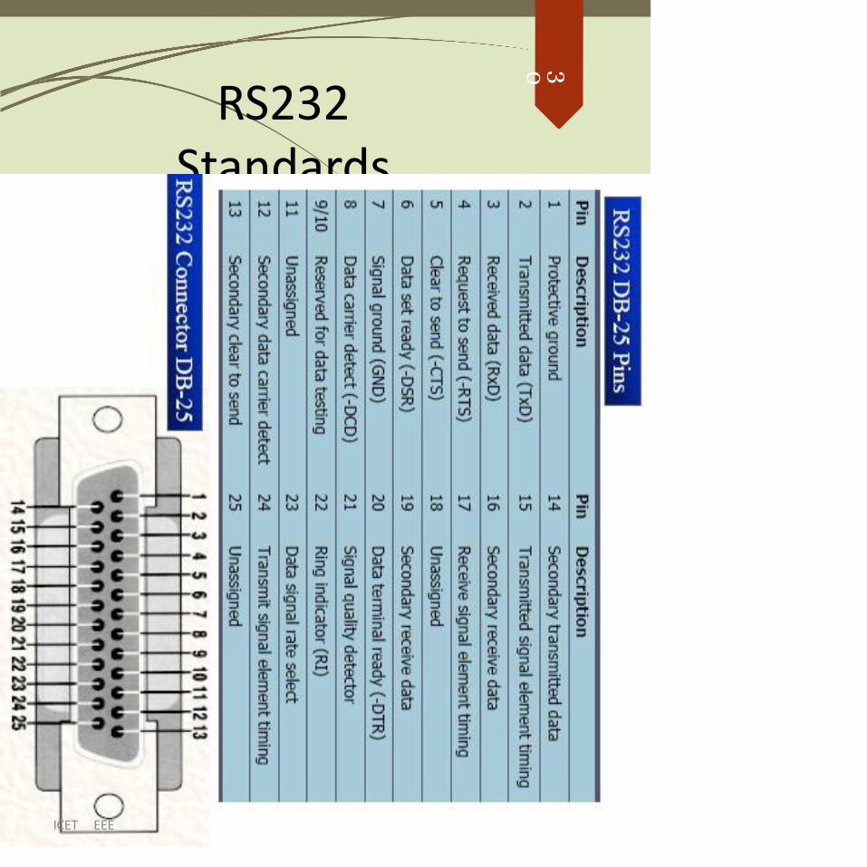
https://arunxeee.blogspot.in
RS232Standards
24
-No
v-177:2
7A
MA
RU
N X
AV
IER
VA
ST
30
ICET EEE
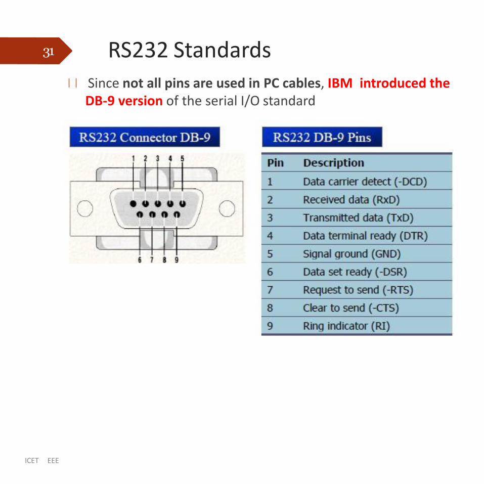
RS232 StandardsSince not all pins are used in PC cables, IBM introduced the DB-9 version of the serial I/O standard
31
ICET EEE
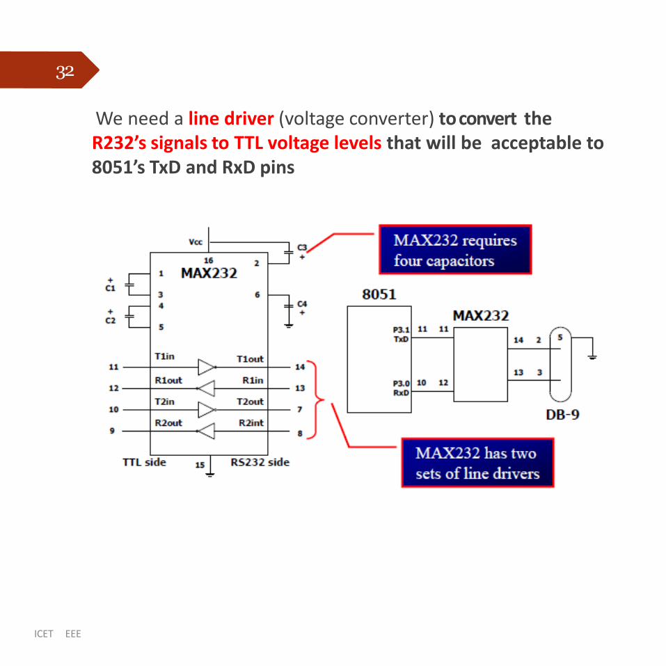
8051 CONNECTION TORS232
ICET EEE
We need a line driver (voltage converter) toconvert the R232’s signals to TTL voltage levels that will be acceptable to 8051’s TxD and RxD pins
32

ICET EEE