Embed Size (px)
Citation preview
Modulation of conductive property in VO2 nano-wires through an air
gap-mediated electric field
Tsubasa Sasaki(Tanaka-lab)2013/10/30

・ BackgroundMetal-insulator transition(MIT) of strongly-correlated electron(Mott) materials (ex. VO2)Electric control of Mott transitionPrevious reports
・ Purpose of my researchW side gate FET
・ PrinciplePLD , Nanoimprint
・ Fabrication・ Experimental result
Atomosphere dependenceChemical equation expectedLaser Raman spectroscopy etc
・ Summary
Contents

Strongly-correlated electron materials VO2
Metal-insulator transition
New electronic devices ex) MottFET ・・・ Electron phase transition is controlled by a gate terminal.
Background
Insulator Metal
Stimulation
TemperatureElectric fieldMagnetic fieldLight
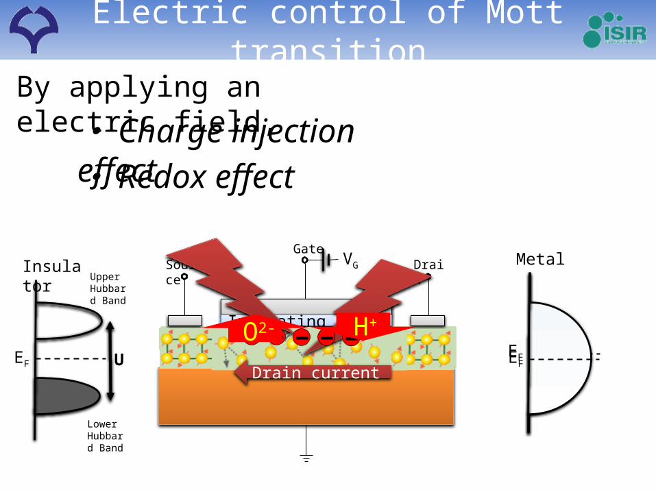
GateDrainSource VG
Insulating layer
Drain current
Electric control of Mott transition
Insulator
EFEFU
Metal
EF
Lower Hubbard Band
Upper Hubbard Band
・ Charge injection effect
・ Redox effect
O2- H+
By applying an electric field,

Features of the transition metal oxide transistors Charge injection effect ( Mott-transistor ) Redox effect ( Redox-transistor: development of two-terminal ReRAM)
J. Jeong et al, Science 339,1402 (2013)
M. Nakano et al, Nature 487,459 (2012)
Previous reports
This time, I have found what using Redox effect.

Gate
Al2O3 sub.
電子相転移雪崩 電子相転移雪崩
Electric field effect simulation ( Cross-sectional view )
Gate Channel
Vacuum
イオンマイグレーション イオンマイグレーション
W side gate type FET structure
Purpose
The physical-properties measurement which combined the probe
microscope etc. is possible.
Measurement by various gas environment is possible.
Advantage

Pulse laser deposition (PLD)
ArF ( λ=193nm )レーザ
基板 レーザ
Al2O3
VO2
Production of thin film
基板
V2O5 焼結体
Pulse laser depositon(PLD)

Production of structure
A
optical micrograph
4mm
4mm
0.5mm
Nanoimprint

A
VO2
Pt
Fabrication
Source
Drain
GateGate d
LW
PLD (Thin films of VO2)
Nanoimprint (Pattern formation of
VO2)
RIE (Etching)
Photolithography (Electrode pattern formation)
Sputtering (Pt electrode)
Source
Drain
GateGate
VO 2 channel

Large resistance change was observed only under the air
Air
N2
DryAir
Atmosphere dependence
The factor is adsorbed water (H2O)
I tried to apply a gate voltage under various atmosphere (Air, N2 and Dry Air)
Humidity:56%
Memory effect
Gradual resistance change

V O2+𝑥2
H 2 O→ V 2 O4+
𝑥2
+𝑥H+ ¿¿Anode :( 陽極 )
Cathode :( 陰極 )
OO
OH H
H
HHe
eChanel
(Cathode)
--
Al2O3
Gate(Anode)
+++++
++----
-
OH HH
H
V2O4+x/2 HxVO2
++
H+
H+
Chemical equation expected
𝑦 H+ ¿+𝑦𝑒−→ 𝑦
2H 2¿
𝑦2
H 2O →𝑦4
O2+𝑦 H+¿+𝑦 𝑒−¿
●
●
●
●
O HH
OO
O
HH
+H
Decrease of resistivity

VO2 resistivity change in the air
Air
Mapping

0 10 20 30 40 500
20
40
60
80
I g-s
(pA
)
Vg (V)
in N2
in Air (humidity 60 )~ %
gate-channel currentThe difference of gate-
channel current
The amount of current flowing along the water which is
adsorbed
The amount of movement of the H+ by electrolysis
N2
Air

Laser Raman spectroscopy
I believed that this is hydrogenated
Jiang Wei et al. Nature Nanotech 70, 357 (2012)
Peak of 199cm-1, 225cm-1, 618cm-1 decreased
0 100 200 300 400 500 600 700 800 900 1000
Inte
nsi
ty (a.
u.)
Raman shift (cm-1)
Hydrogenated VO2
Pure VO2
Annealed in a hydrogen atmosphere
30 35 40 45 50 55 60 65 700
200
400
600
800
Inte
nsity
(a.
u.)
distance (m)
20 25 30 35 40 45 50 55 60
0
200
400
600In
ten
sity
(a
.u.)
distance (m)
HydrogenatedPeak area of 600 cm-1 near
Hydrogen ions are diffused over the entire channel width(3μm)
gate gate gate gate
channelchannel

H 𝑥V O2
Large resistance change by hydrogen doped
Insulator
EF U
Lower Hubbard Band
Upper Hubbard Band
EF
Metal
EF

Large resistance change was observed only in the air⇒The factor is adsorbed water (H2O)⇒Hydrogenation of VO2 by the gate electric field
●
Summary
●
I was fabricated W side gate type FET structure
⇒Redox-controlled Mott transistor
Future plan
Summary
● I will perform the SIMS measurement to confirm hydrogen existence in the VO2 channel

Thank you for your attention


![TANAKA Al 130 17- ] Tanaka Ai Europe B.V. Color Business Center …tanakaai.co.jp/news/img/news_0602.pdf · 2020. 3. 3. · TANAKA Al 130 17-_] Tanaka Ai Europe B.V. Color Business](https://img.pdfslide.us/doc/110x75/5fe30b4595c1ae2baf7f970a/tanaka-al-130-17-tanaka-ai-europe-bv-color-business-center-2020-3-3-tanaka.jpg)