Embed Size (px)
Citation preview
Modern VLSI Design 2e: Chapter 7 Copyright 1998 Prentice Hall PTR
Topics
Block placement. Global routing. Switchbox routing.

Modern VLSI Design 2e: Chapter 7 Copyright 1998 Prentice Hall PTR
Floorplanning strategies
Floorplanning must take into account blocks of varying function, size, shape.
Must design:– space allocation;– signal routing;– power supply routing;– clock distribution.
Modern VLSI Design 2e: Chapter 7 Copyright 1998 Prentice Hall PTR
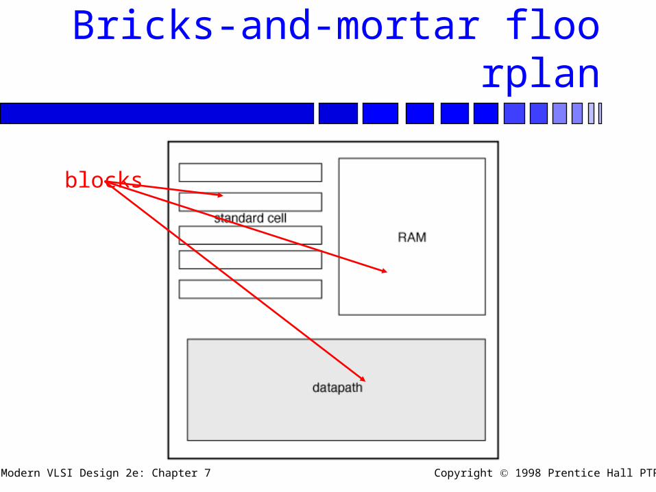
Bricks-and-mortar floorplan
blocks
Modern VLSI Design 2e: Chapter 7 Copyright 1998 Prentice Hall PTR
Purposes of floorplanning
Early in design:– Prepare a floorplan to budget area, wire area/del
ay. Tradeoffs between blocks can be negotiated. Late in design:
– Make sure the pieces fit together as planned.– Implement the global layout.

Modern VLSI Design 2e: Chapter 7 Copyright 1998 Prentice Hall PTR
Types of routing
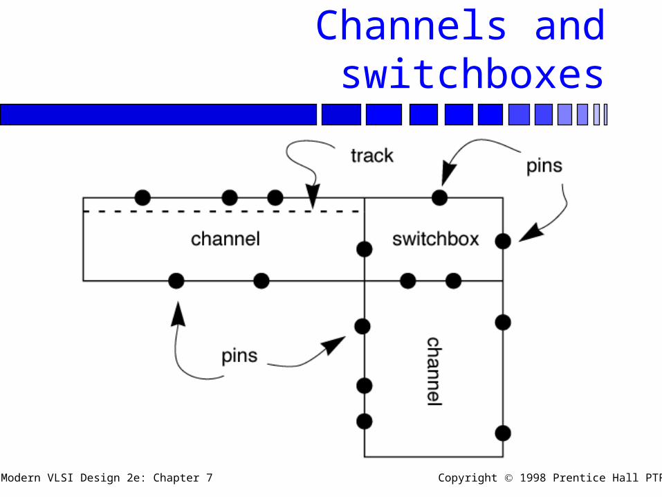
Channel routing:– channel may grow in one dimension to
accommodate wires;– pins generally on only two sides.
Switchbox routing:– cannot grow in any dimension;– pins are on all four sides, fixing dimensions of
the box.
Modern VLSI Design 2e: Chapter 7 Copyright 1998 Prentice Hall PTR
Channels and switchboxes

Modern VLSI Design 2e: Chapter 7 Copyright 1998 Prentice Hall PTR
Block placement
Blocks have:– area;– aspect ratio.
Blocks may be placed at different rotations and reflections.
Uniform size blocks are easier to interchange.
Modern VLSI Design 2e: Chapter 7 Copyright 1998 Prentice Hall PTR
Blocks and wiring
Cannot ignore wiring during block placement - large wiring areas may force rearrangement of blocks.
Wiring plan must consider area and delay of critical signals.
Blocks divide wiring area into routing channels.
Modern VLSI Design 2e: Chapter 7 Copyright 1998 Prentice Hall PTR
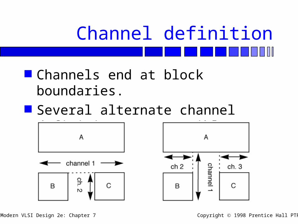
Channel definition
Channels end at block boundaries. Several alternate channel definitions are
possible:
Modern VLSI Design 2e: Chapter 7 Copyright 1998 Prentice Hall PTR
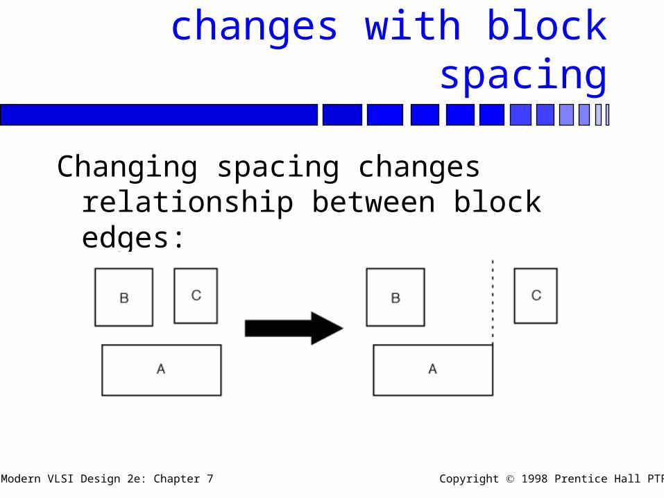
Channel definition changes with block spacing
Changing spacing changes relationship between block edges:
Modern VLSI Design 2e: Chapter 7 Copyright 1998 Prentice Hall PTR
Modern VLSI Design 2e: Chapter 7 Copyright 1998 Prentice Hall PTR
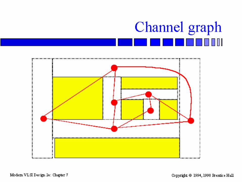
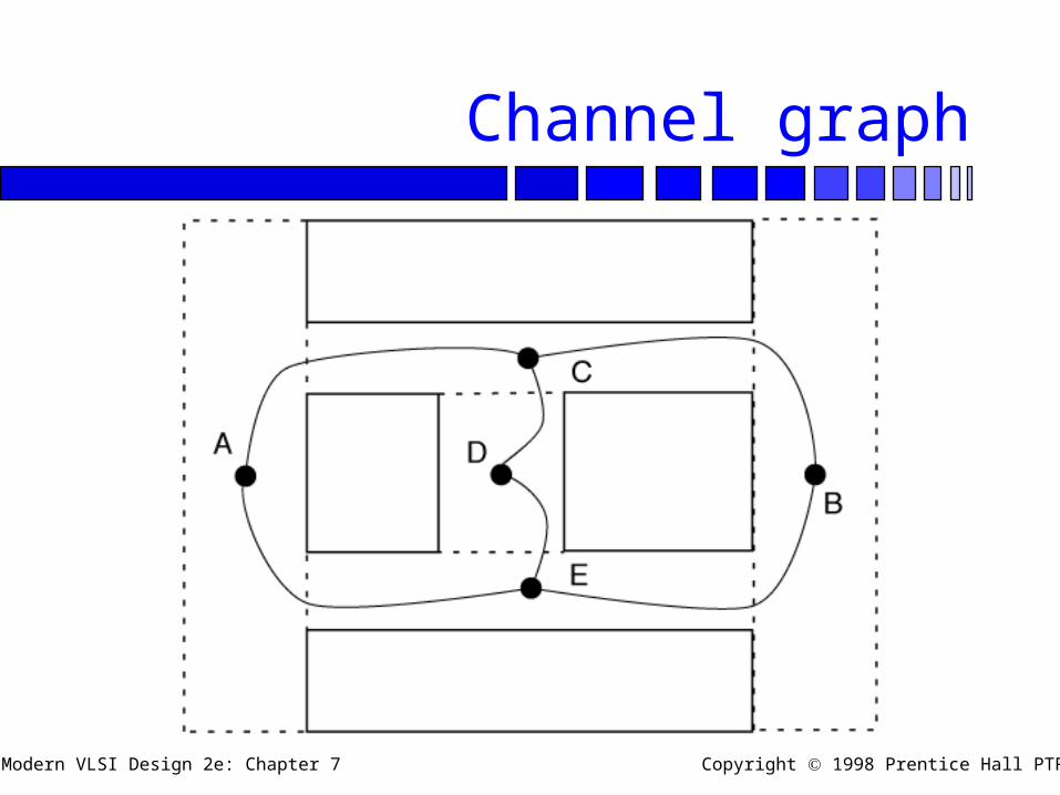
Channel graph

Modern VLSI Design 2e: Chapter 7 Copyright 1998 Prentice Hall PTR
Channel graph usage
Nodes are channels, edges placed between two channels that touch.
Channel graph shows paths between channels.
Channel graph can be used to guide global routing.

Modern VLSI Design 2e: Chapter 7 Copyright 1998 Prentice Hall PTR
Channels must be routed in order
Wire out of end of one channel creates pin on side of next channel:
channel A
channel B
constraint

Modern VLSI Design 2e: Chapter 7 Copyright 1998 Prentice Hall PTR
Windmills
Can create an unroutable combination of channels with circular constraints:

Modern VLSI Design 2e: Chapter 7 Copyright 1998 Prentice Hall PTR
Modern VLSI Design 2e: Chapter 7 Copyright 1998 Prentice Hall PTR
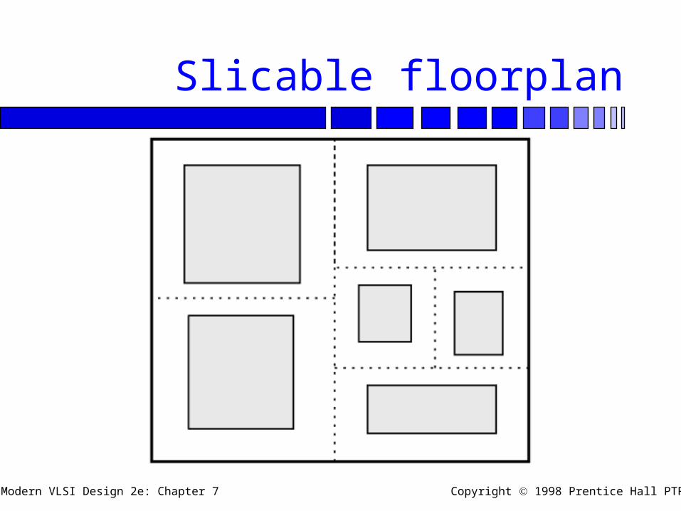
Slicable floorplan

Modern VLSI Design 2e: Chapter 7 Copyright 1998 Prentice Hall PTR
Slicability property
A slicable floorplan can be recursively cut in two without cutting any blocks.
A slicable floorplan is guaranteed to have no windmills, therefore guaranteed to have a feasible order of routing for the channels.
Slicability is a desirable property for floorplans.
Modern VLSI Design 2e: Chapter 7 Copyright 1998 Prentice Hall PTR
Global routing
Goal: assign wires to paths through channels.
Don’t worry about exact routing of wires within channel.
Can estimate channel height from global routing using congestion.

Modern VLSI Design 2e: Chapter 7 Copyright 1998 Prentice Hall PTR
Line probe routing
Heuristic method for finding a short route. Works with arbitrary combination of
obstacles. Does not explore all possible paths - not
optimal.

Modern VLSI Design 2e: Chapter 7 Copyright 1998 Prentice Hall PTR
Line probe example
A
Aline 1
line 2
Modern VLSI Design 2e: Chapter 7 Copyright 1998 Prentice Hall PTR
Channel utilization
Want to keep all channels about equally full to minimize wasted area.
Important to route time-critical signals first. Shortest path may not be best for global
wiring. In general, may need to rip-up wires and
reroute to improve the global routing.
Modern VLSI Design 2e: Chapter 7 Copyright 1998 Prentice Hall PTR
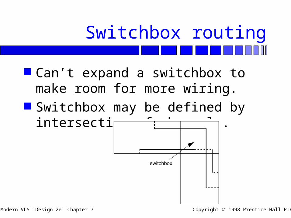
Switchbox routing
Can’t expand a switchbox to make room for more wiring.
Switchbox may be defined by intersection of channels.
Modern VLSI Design 2e: Chapter 7 Copyright 1998 Prentice Hall PTR
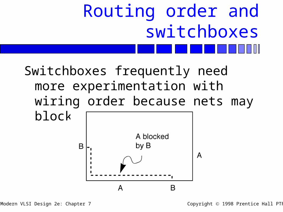
Routing order and switchboxes
Switchboxes frequently need more experimentation with wiring order because nets may block other nets: