Embed Size (px)
Citation preview
Modern DRAM Memory Architectures
Sam Miller
Tam Chantem
Jon Lucas
CprE 585 Fall 2003
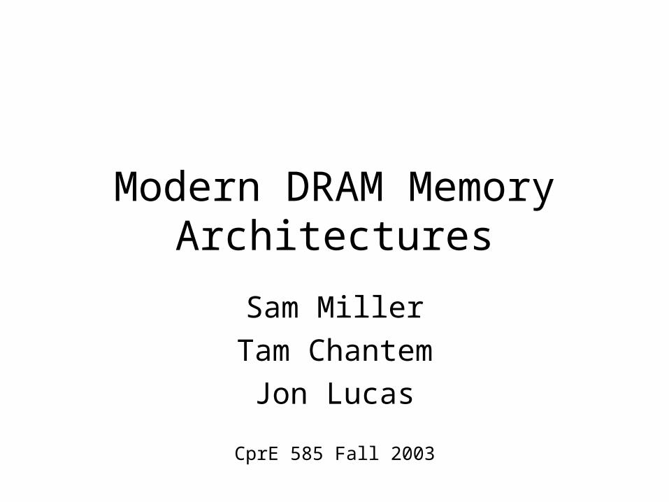
Introduction
• Memory subsystem is a bottleneck• Memory stall time will become dominant• New architectures & accessing techniques
proposed to combat these issues
Outline
• DRAM background
• Introduction to Memory Access Scheduling
• Fine-grain priority scheduling
• Review of DRAM architectures
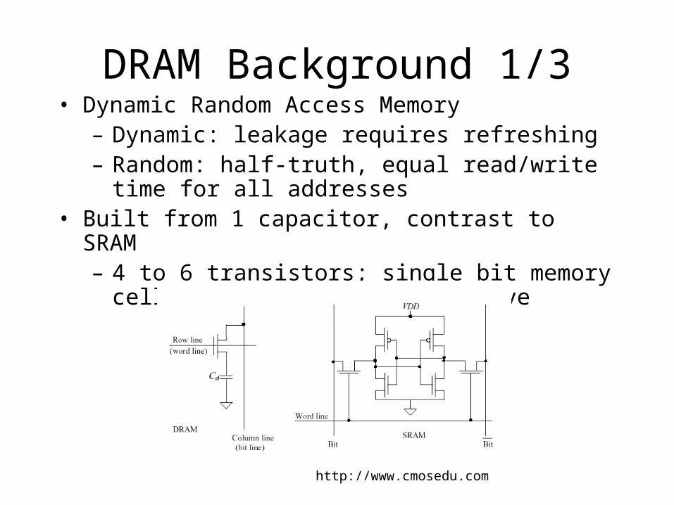
DRAM Background 1/3• Dynamic Random Access Memory
– Dynamic: leakage requires refreshing– Random: half-truth, equal read/write time for all
addresses• Built from 1 capacitor, contrast to SRAM
– 4 to 6 transistors; single bit memory cell is larger & more expensive
http://www.cmosedu.com

DRAM Background 2/3
• Accessing DRAM– Think of a square grid: split address in half– Half bits for row, other half for column
• Today, most architectures multiplex address pins– Read row & column address on two edges– Saves space, money
• Typically there are more columns than rows– Better row buffer hit rate– Less time spent refreshing (just a row read)
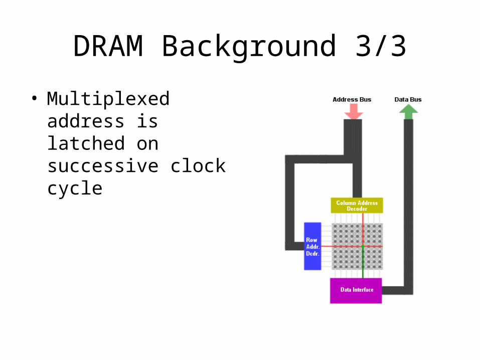
DRAM Background 3/3
• Multiplexed address is latched on successive clock cycle

3-D DRAM Representation
S. Rixner et al. Memory Access Scheduling. ISCA 2000.
DRAM Operations
• Precharge– Desired row is read into row buffer on a
miss
• Row Access– Bank is already precharged
• Column Access– Desired column can be accessed by row
buffer
Memory Access Scheduling 1/3
• Similar to out-of-order execution
• Scheduler determines which set of pending references can best utilize the available bandwidth
• Simplest policy is “in-order”
• Another policy is “column first” – Reduces access latency to valid rows
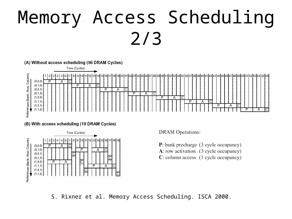
Memory Access Scheduling 2/3
S. Rixner et al. Memory Access Scheduling. ISCA 2000.
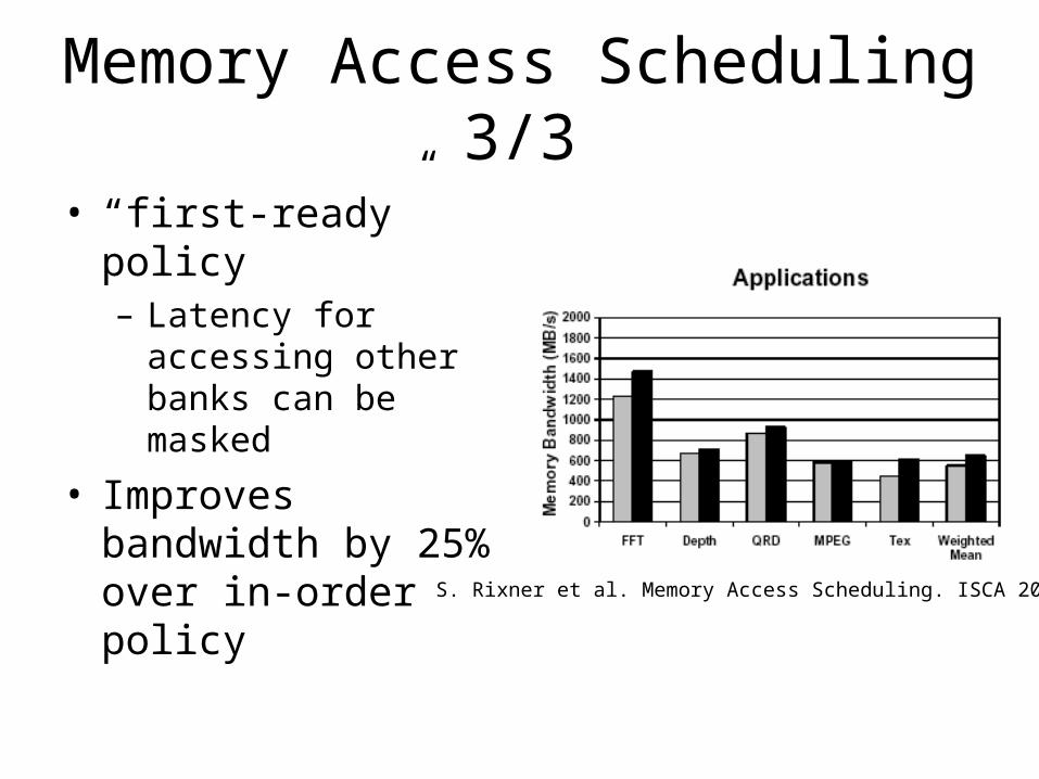
Memory Access Scheduling 3/3
• “first-ready” policy– Latency for accessing
other banks can be masked
• Improves bandwidth by 25% over in-order policy
S. Rixner et al. Memory Access Scheduling. ISCA 2000.
Fine-grain Priority Scheduling 1/5
• Goal: workload independent, optimal performance on multi-channel memory systems
• On the highest level cache miss, DRAM is issued a “cache line fill request”– Typically, more data is fetched than needed– But it may be needed in the future
• For a performance increase, divide requests into sub-blocks with priority tags
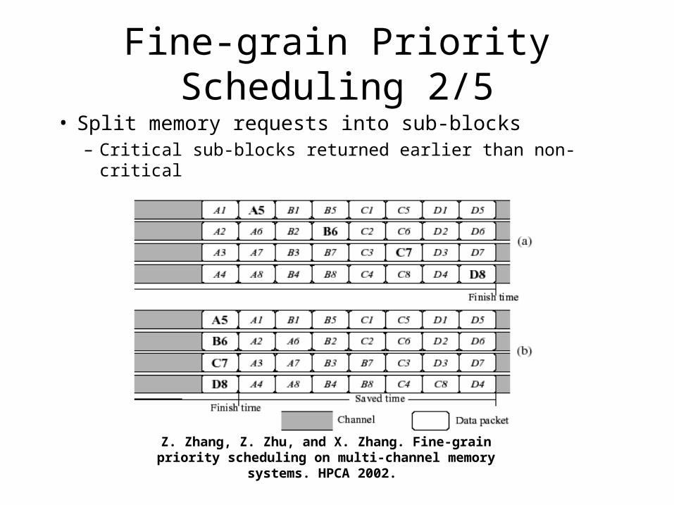
Fine-grain Priority Scheduling 2/5
• Split memory requests into sub-blocks– Critical sub-blocks returned earlier than non-critical
Z. Zhang, Z. Zhu, and X. Zhang. Fine-grain priority scheduling on multi-channel memory systems. HPCA 2002.

Fine-grain Priority Scheduling 3/5
• Sub-block size can be no less than minimum DRAM request length
• 16 bytes is smallest size for DRDRAM
• Note: memory misses on other sub-blocks of the SAME cache block may happen– Priority information is updated dynamically in
this case by the Miss Status Handling Register (MSHR)
Fine-grain Priority Scheduling 4/5
• Complexity issues– Support multiple outstanding, out-of-order
memory requests– Data returned to processor in sub-block, not
cache-block– Memory controller must be able to order
DRAM operations from multiple outstanding requests
Fine-grain Priority Scheduling 5/5
• Compare to gang scheduling– Cache block size used as burst size– Memory channels grouped together– Stalled instructions resumed when whole cache block
is returned
• Compare to burst scheduling– Each cache miss results in multiple DRAM requests– Each request is confined to one memory channel
Contemporary DRAM Architectures 1/5
• Many new DRAM architectures have been introduced to improve memory sub-system performance
• Goals– Improved bandwidth– Reduced latency
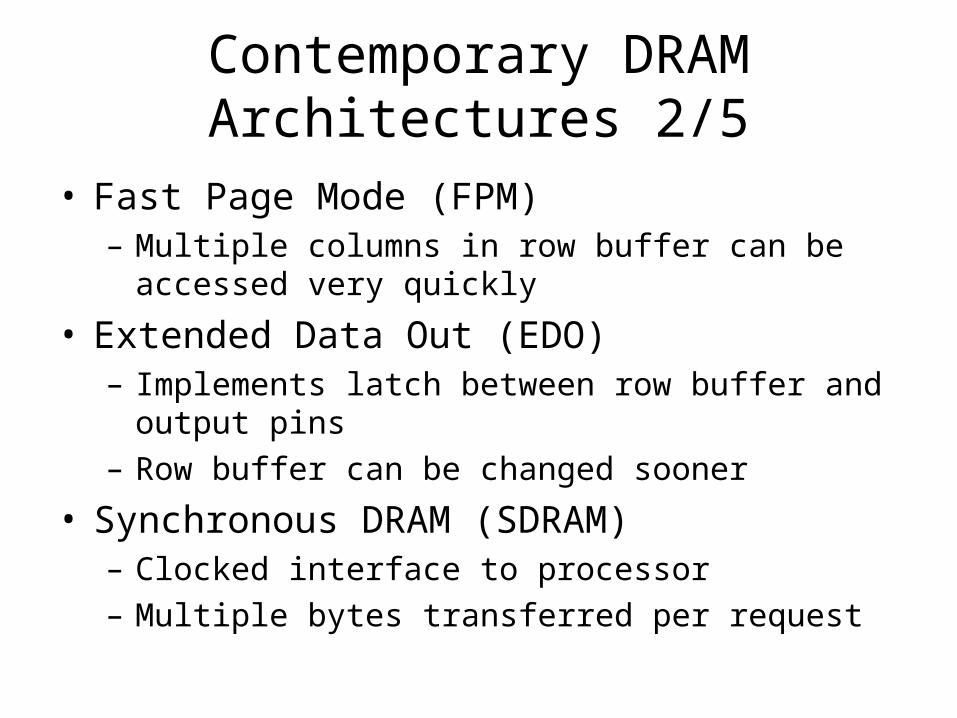
Contemporary DRAM Architectures 2/5
• Fast Page Mode (FPM)– Multiple columns in row buffer can be accessed very
quickly
• Extended Data Out (EDO)– Implements latch between row buffer and output pins– Row buffer can be changed sooner
• Synchronous DRAM (SDRAM)– Clocked interface to processor– Multiple bytes transferred per request
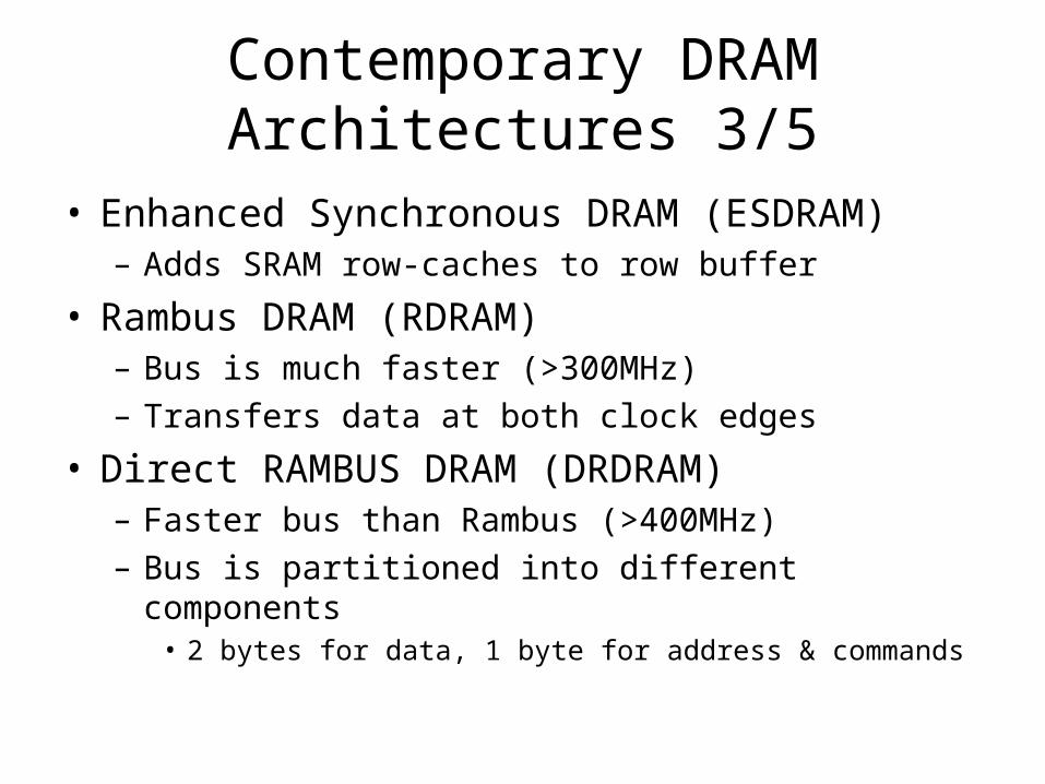
Contemporary DRAM Architectures 3/5
• Enhanced Synchronous DRAM (ESDRAM)– Adds SRAM row-caches to row buffer
• Rambus DRAM (RDRAM)– Bus is much faster (>300MHz)– Transfers data at both clock edges
• Direct RAMBUS DRAM (DRDRAM)– Faster bus than Rambus (>400MHz)– Bus is partitioned into different components
• 2 bytes for data, 1 byte for address & commands

Contemporary DRAM Architectures 4/5
V. Cuppu, B. Jacob, B. Davis, and T. Mudge. A performance comparison of contemporary DRAM architectures. ISCA 1999.
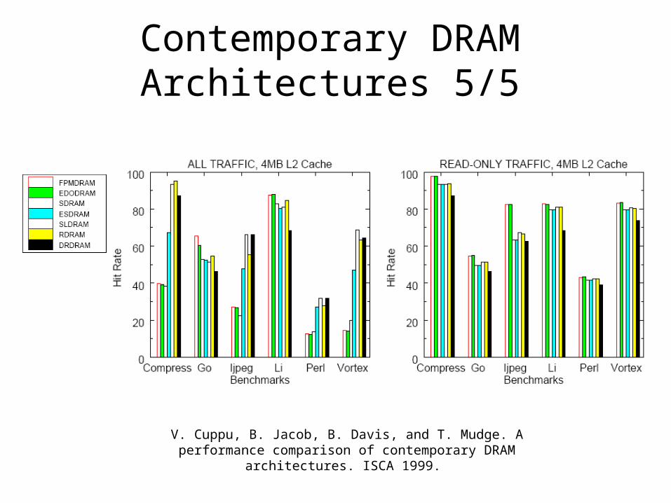
Contemporary DRAM Architectures 5/5
V. Cuppu, B. Jacob, B. Davis, and T. Mudge. A performance comparison of contemporary DRAM architectures. ISCA 1999.