Embed Size (px)
Citation preview

Chapter 3 Modelling of Three-Phase Shunt Hybrid active Power filter 77
Ph.D Thesis submitted to Jawaharlal Nehru Technological University Anantapur, Anantapur
CHAPTER 3
MODELLING OF THREE-PHASE SHUNT HYBRID
ACTIVE POWER FILTER
3.1 INTRODUCTION
The three-phase Shunt hybrid APF topology for harmonic mitigation in low
and medium voltage power distribution systems consists of a VSI based three phase
shunt active filter (SAF) and tuned passive filters (TPF) connected in parallel with the
load. This chapter discusses the modelling of shunt active filter and design of filter
interfacing inductor, DC bus capacitor, tuned passive filters. It also presents the
analysis of synchronous reference frame theorem to estimate the compensation
reference current and hysteresis current controller for switching signal generation for
SAF. In addition the principle of operation of asymmetric cascaded multilevel inverter
used as SAF in medium voltage power distribution system and modulation strategy of
MLI is also presented.
3.2 OPERATION PRINCIPLE OF THE PROPOSED SHUNT
HYBRID APF TOPOLOGY
The operation principle of the proposed shunt hybrid APF topology is
illustrated in Fig. 3.1. It consists of a shunt active filter and tuned passive filters
(TPFs) connected in parallel with the nonlinear load which is connected to ac source.
The two TPFs are designed to absorb 5th
and 7th
harmonic currents with the principle
of series resonance and SAF compensates remaining harmonics. The SAF generates
compensation current (if) equal to harmonic load current (iLh) but in opposite phase to

Chapter 3 Modelling of Three-Phase Shunt Hybrid active Power filter 78
Ph.D Thesis submitted to Jawaharlal Nehru Technological University Anantapur, Anantapur
it and injects in to the point of common coupling (PCC) through an interfacing
inductor. Therefore source current (is) is desired to be sinusoidal and in phase with the
source voltage (vs) to yield maximum power factor. The SAF is a VSI and a capacitor
connected on the DC side acts as storage element.
Fig. 3.1 Operation principle of the proposed Shunt Hybrid APF.
3.3 THREE PHASE SHUNT ACTIVE FILTER MODEL
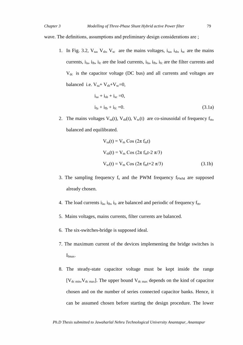
The basic SAF scheme considered is depicted in Fig. 3.2. Practically, it is a
three phase AC/DC boost converter, where the main energy storage element is
provided by the capacitor C and the inductors L are used to control the filter currents
by means of the converter voltages. Conversely to the case of a pure voltage
converter, the focus for such type of device is on the currents injected into the line
which have to compensate for harmonics generated by nonlinear loads. The capacitor
voltage has to be constrained into a safe range while it is unimportant the shape of its
Chapter 3 Modelling of Three-Phase Shunt Hybrid active Power filter 79
Ph.D Thesis submitted to Jawaharlal Nehru Technological University Anantapur, Anantapur
wave. The definitions, assumptions and preliminary design considerations are ;
1. In Fig. 3.2, Vsa, Vsb, Vsc are the mains voltages, isa, isb, isc are the mains
currents, ila, ilb, ilc are the load currents, ifa, ifb, ifc are the filter currents and
Vdc is the capacitor voltage (DC bus) and all currents and voltages are
balanced i.e. Vsa+ Vsb+Vsc=0,
isa + isb + isc =0,
ifa + ifb + ifc =0. (3.1a)
2. The mains voltages Vsa(t), Vsb(t), Vsc(t) are co-sinusoidal of frequency fm,
balanced and equilibrated.
Vsa(t) = Vm Cos (2π fmt)
Vsb(t) = Vm Cos (2π fmt-2 π/3)
Vsc(t) = Vm Cos (2π fmt+2 π/3) (3.1b)
3. The sampling frequency fs and the PWM frequency fPWM are supposed
already chosen.
4. The load currents ila, ilb, ilc are balanced and periodic of frequency fm.
5. Mains voltages, mains currents, filter currents are balanced.
6. The six-switches-bridge is supposed ideal.
7. The maximum current of the devices implementing the bridge switches is
Ifmax.
8. The steady-state capacitor voltage must be kept inside the range
[Vdc min,Vdc max]. The upper bound Vdc max depends on the kind of capacitor
chosen and on the number of series connected capacitor banks. Hence, it
can be assumed chosen before starting the design procedure. The lower
Chapter 3 Modelling of Three-Phase Shunt Hybrid active Power filter 80
Ph.D Thesis submitted to Jawaharlal Nehru Technological University Anantapur, Anantapur
bound Vdc min depends on the controllability constraints.
Fig. 3.2 Three phase shunt active filter scheme.
Let , Vs(t)=[Vsa(t) Vsb(t) Vsc(t)]T mains voltage vector;
VfK(t)=[Vfxk(t) Vfyk(t) Vfzk(t)]T voltage vector between leg
centers and the node K;
Vabc(t)=VfN(t)=[VfxN(t) VfyN(t) VfzN(t)]T voltage vector
between leg centers and the node N;
ifabc (t) = [ifa(t) ifb(t) ifc(t)] filter current vector;
isabc (t) = [isa(t) isb (t) isc(t)] source current vector;
ilabc (t) = [ila(t) ilb (t) ilc(t)] load current vector;
Uxyz(t)=[ux(t) uy(t) uz(t)]T control inputs of the six-
switches-bridge, where ux є {0,1}, x = a,b,c. (3.2)
By means of Kirchoff laws it is possible to express the vector Vabc as

Chapter 3 Modelling of Three-Phase Shunt Hybrid active Power filter 81
Ph.D Thesis submitted to Jawaharlal Nehru Technological University Anantapur, Anantapur
Va = Vsa- L 𝑑𝑖𝑎
𝑑𝑡 - Ria = SaVdc - VNK (3.3a)
Vb = Vsb- L 𝑑𝑖𝑏
𝑑𝑡 – Rib = SbVdc - VNK (3.3b)
Vc = Vsc- L 𝑑𝑖𝑐
𝑑𝑡 – Ric = ScVdc - VNK (3.3c)
C dV dc
dt = Saifa + Sbifb + Scifc (3.3d)
where Sa , Sb , Sc are the logic states of the switches, whose value is 1 when the
positive switch is on and 0 when negative switch is conducting. Therefore the
following relations hold good.
Sa = 0 → Vak = 0
= 1 = Vdc
Sb = 0 → Vbk = 0
= 1 = Vdc
Sc = 0 → Vck = 0
= 1 = Vdc
Also L and C are the inductors and capacitor values while R is the parasitic
resistance. Summing the first three scalar equations of (3.3) and considering equation
(3.1a) the value of VNK can be recovered as:
VNK = Sa +Sb +Sc
3 Vdc (3.4)
By means of equations (3.4), the above equations (3.3) can be rearranged as:
di a
dt = -
R
L ia -
Vdc
L (Sa -
Sa +Sb +Sc
3 ) +
1
L Vsa
di b
dt = -
R
L ib -
Vdc
L (Sb -
Sa +Sb +Sc
3 ) +
1
L Vsb

Chapter 3 Modelling of Three-Phase Shunt Hybrid active Power filter 82
Ph.D Thesis submitted to Jawaharlal Nehru Technological University Anantapur, Anantapur
di c
dt = -
R
L ic -
Vdc
L (Sc -
Sa +Sb +Sc
3 ) +
1
L Vsc
dV dc
dt =
1
C [Saifa + Sbifb + Scifc] (3.5)
Looking at the previous equation (3.5) it is quite natural to define three new control
functions ua, ub and uc as:
ua = Sa - Sa +Sb +Sc
3 =
2
3 Sa -
1
3 Sb -
1
3 Sc
ub = Sb - Sa +Sb +Sc
3 = -
1
3 Sa -
2
3 Sb -
1
3 Sc
uc = Sc - Sa +Sb +Sc
3 =-
1
3 Sa -
1
3 Sb -
2
3 Sc (3.6)
It is worth to point out that the previous logic functions Sj represent the
normalized voltages VjK with respect to the DC-link voltage Vdc while the new control
functions represents the normalized voltages Vj that are referred to node N. Looking
at the previous equation it is possible to express the relation between logic functions
and control functions in a more compact way as:
uabc = uTS Sabc with
uabc =
ua
ub
uc
; Sabc =
sa
sb
sc
; uTS =
−
2
3−
1
3−
1
31
3
2
3−
1
3−1
3−
1
3
2
3
By means of equations (3.6), elaborating equations (3.5) it can be readily obtained:
di a
dt = -
R
L ia -
Vdc
L ua+
1
L Vsa
di b
dt = -
R
L ib -
Vdc
L ub +
1
L Vsb
di c
dt = -
R
L ic -
Vdc
L uc +
1
L Vsc

Chapter 3 Modelling of Three-Phase Shunt Hybrid active Power filter 83
Ph.D Thesis submitted to Jawaharlal Nehru Technological University Anantapur, Anantapur
dV dc
dt =
1
C [uaifa + ubifb + ucifc] (3.7)
Substantially this last model differs from the previous one for the different definitions
of the control vector u instead of logic one S.
3.4 PROPOSED SHAF FOR HARMONIC COMPENSATION IN
LV POWER DISTRIBUTION SYSTEM
The low voltage power distribution system of interest consists of a three
phase, 2000 V (r.m.s), 50 Hz sinusoidal AC voltage source. The source inductor is
considered as Ls. A full-bridge diode rectifier with R-L load is selected as the
nonlinear load as shown in Fig. 3.3.
Fig. 3.3 System configuration with the proposed SHAPF.
This type of load can be found in most power electronics applications, i.e.
Chapter 3 Modelling of Three-Phase Shunt Hybrid active Power filter 84
Ph.D Thesis submitted to Jawaharlal Nehru Technological University Anantapur, Anantapur
switch-mode power supply, uninterruptible power supply (UPS), AC motor drive and
DC servo drive. It is used to convert the input AC to DC in an uncontrolled manner. It
is well known that this nonlinear load draws highly distorted current from the
distribution source, thus a major source of harmonic distortion [9]. The proposed
shunt hybrid APF is connected with the distribution line at the PCC through an
interfacing inductor (Lf). This interfacing inductor provides isolation from the
distribution line. A large interfacing inductor is preferable because it results in small
switching ripple. However, the large interfacing inductor limits the dynamic response
of the compensation current. Therefore, there is a compromise involved in sizing the
interfacing inductor. This VSI uses DC-bus capacitor (Cdc) as the supply source and
switches at high-frequency to generate a compensation current that follows the
estimated reference current. Therefore the voltage across the DC-bus capacitor (Vdc)
must be maintained at a constant value that is higher than the amplitude of the source
voltage.
3.4.1 Power Circuit
The power circuit used in the proposed hybrid APF is an universal full-bridge
VSI as shown in Fig. 3.3. The VSI consists of six transistors, each connected to an
anti-parallel diode. The transistors are the metal oxide semiconductor field effect
transistors (MOSFETs). They are selected due to their superior performance
characteristics, i.e. low forward voltage drop, fast switching times and high power
handling capability. The logic inverters ensure that each MOSFET on the same leg
complement each other avoiding short circuit problem of the DC-bus capacitor (Cdc).
3.4.2 Interfacing Inductor
The desired compensation current waveform is obtained by controlling the
Chapter 3 Modelling of Three-Phase Shunt Hybrid active Power filter 85
Ph.D Thesis submitted to Jawaharlal Nehru Technological University Anantapur, Anantapur
switching of the MOSFETs in the VSI. The switching ripple (isw) of the compensation
current is determined by the size of the interfacing inductor, available driving voltage
across the interfacing inductor, and switching frequency. In the proposed scheme, the
driving voltage is the DC-bus voltage (Vdc). The bipolar DC-bus voltage across the
interfacing inductor determines the peak-to-peak switching ripple (∆Isw,p−p).The
minimum interfacing inductor (Lf ,min) can be calculated as
Lf.min =Vdc
2. ΔIsw .p−p .fsw ,max (3.8)
where f sw,max is the maximum frequency of switching ripple and ∆Isw, p− p is the peak-
to-peak switching ripple of compensation current. The detailed derivation of (3.8) is
presented in Appendix A.
3.4.3 DC-Bus Capacitor
The DC-bus capacitor (Cdc) is used as a temporary energy storage element in
the proposed hybrid APF as shown in Fig. 3.3. Under steady state condition, the
reactive and harmonic load currents will charge and discharge the DC-bus capacitor
during the source voltage period. The total reactive and harmonic load current to be
compensated is the principle factor that causes the DC-bus capacitor voltage
fluctuation. To get a good compensation performance, serious voltage fluctuations
must be avoided. In such cases the capacitor may have to supply real power demand
of the load during one cycle of the utility voltage. This can be achieved by proper
sizing of the DC-bus capacitor. The size determination of the DC-bus capacitor is
based on the energy-balance principle which means that the stored energy of the
capacitor should be equal to sudden change in the load energy for one cycle of supply
voltage.

Chapter 3 Modelling of Three-Phase Shunt Hybrid active Power filter 86
Ph.D Thesis submitted to Jawaharlal Nehru Technological University Anantapur, Anantapur
Let Vdc(t) be the DC-bus voltage at that instant(maximum or minimum), Vdc,ref
is the DC-bus reference voltage, Vsmax is the peak value of the source voltage, ∆IL is
the change in peak value of the harmonic load current and T is the time period of
source voltage. Then change in energy due to change in load per one cycle is
ΔEL(t) = 1
2. Vsmax . ΔIL.T
and stored energy in the capacitor is given by
ΔEc(t) = 1
2Cdc Vdc .ref
2 − Vdc (t) 2
Therefore stored energy of the capacitor should supply change in load energy for one
time period.
∴ ΔEc(t) = ΔEL(t)
1
2Cdc Vdc .ref
2 − Vdc (t) 2 =1
2. Vsmax . ΔIL.T (3.9)
Therefore three capacitor voltage values are obtained on the basis of the following
three situations:
i) When there is a sudden increase in the fundamental load current (Cdc1):
1
2Cdc Vdc .ref
2 − Vdc ,min 2 =
1
2. Vsmax . ΔIL1. T
where Vdc,min is the minimum value of DC bus voltage.
ii) When there is a sudden decrease in the fundamental load current (Cdc2):
1
2Cdc Vdc .max 2 − Vdc ,ref
2 =
1
2. Vsmax . ΔIL2 T
iii) Reactive and harmonic currents of load current during steady state(Cdc3):
1
2Cdc ΔVdc .
2 − Vdc ,ref 2 =
1
2. Vsmax . ΔIL3 T
where ΔVdc is the maximum or minimum value of Vdc.
The largest value of Cdc1, Cdc2, Cdc3 will be selected. For compensating
Chapter 3 Modelling of Three-Phase Shunt Hybrid active Power filter 87
Ph.D Thesis submitted to Jawaharlal Nehru Technological University Anantapur, Anantapur
harmonics and reactive power Cdc3 is selected in this thesis. Therefore the
size of DC-bus capacitor is determined by
Cdc ≥ Vsmax ΔIL T
ΔVdc 2− Vdc ,ref 2 (3.10)
3.4.4
The objective the control strategy of the proposed three-phase shunt hybrid
active filter is to produce appropriate gating signals for the switching transistors of
VSI. The control system consists of synchronous reference frame theorem based
compensation current estimator, hysteresis current controller for gate signal
generation and a Fuzzy logic controller to maintain the DC bus voltage constant.
3.4.4.1 Compensation Current Reference Estimation Using d-q-0
Theory
In this work synchronous reference frame (SRF) theory is employed to obtain
compensating current reference signal. In this control strategy three phase load
currents are sensed and transformed from a-b-c reference frame to d-q coordinates
which are DC components using park‟s transformation. Passing these d-q components
of load currents through low pass filter, the low frequency fundamental components
only will be passed through and harmonic component is stopped. By subtracting
fundamental component from non-filtered signal will result in harmonic component in
load current. Control signal from Fuzzy logic controller is added to this signal to
obtain the reference compensating signal in d-q reference frame. By transforming
these components in d-q reference to a-b-c reference frame using inverse Park‟s
transformation, the information about harmonic current component in a-b-c reference
frame is obtained.
Chapter 3 Modelling of Three-Phase Shunt Hybrid active Power filter 88
Ph.D Thesis submitted to Jawaharlal Nehru Technological University Anantapur, Anantapur
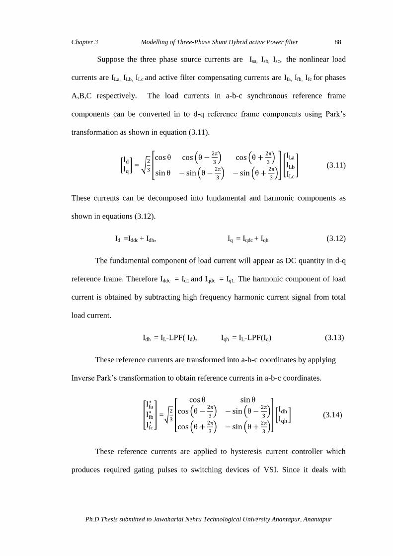
Suppose the three phase source currents are Isa, Isb, Isc, the nonlinear load
currents are ILa, ILb, ILc and active filter compensating currents are Ifa, Ifb, Ifc for phases
A,B,C respectively. The load currents in a-b-c synchronous reference frame
components can be converted in to d-q reference frame components using Park‟s
transformation as shown in equation (3.11).
Id
Iq =
2
3 cos θ cos θ −
2π
3 cos θ +
2π
3
sin θ − sin θ −2π
3 − sin θ +
2π
3
ILa
ILb
ILc
(3.11)
These currents can be decomposed into fundamental and harmonic components as
shown in equations (3.12).
Id =Iddc + Idh, Iq = Iqdc + Iqh (3.12)
The fundamental component of load current will appear as DC quantity in d-q
reference frame. Therefore Iddc = Id1 and Iqdc = Iq1. The harmonic component of load
current is obtained by subtracting high frequency harmonic current signal from total
load current.
Idh = IL-LPF( Id), Iqh = IL-LPF(Iq) (3.13)
These reference currents are transformed into a-b-c coordinates by applying
Inverse Park‟s transformation to obtain reference currents in a-b-c coordinates.
Ifa∗
Ifb∗
Ifc∗ =
2
3
cos θ sin θ
cos θ −2π
3 − sin θ −
2π
3
cos θ +2π
3 − sin θ +
2π
3
Idh
Iqh (3.14)
These reference currents are applied to hysteresis current controller which
produces required gating pulses to switching devices of VSI. Since it deals with

Chapter 3 Modelling of Three-Phase Shunt Hybrid active Power filter 89
Ph.D Thesis submitted to Jawaharlal Nehru Technological University Anantapur, Anantapur
mainly DC quantities and computation is instantaneous this theory is considered in
this thesis for estimating reference compensating current.
3.4.4.2 Hysteresis Current Control (HCC) for Switching Signal
Generation
Fig. 3.4(a) shows a single phase VSI with terminal voltage (Vf)
connected to a sinusoidal voltage source (Vs) through an equivalent
inductance L and resistance R. Fig. 3.4(b) shows it‟s HCC.
Fig. 3.4 (a) Single phase VSI and ( b ) Its hysteresis current controller.
To control APF output current (if) and to track certain reference current if*,
according to Fig. 3.4(a), the instantaneous voltage equation is:
L di f
dt + if R = Vf - Vs (3.15)
When the APF output current is equal to reference current if∗, the corresponding
equation will be
L di f
∗
dt + if
∗ R = Vf∗ - Vs (3.16)
where Vf∗ is the reference VSI terminal voltage corresponding to if
∗. If APF current
tracking error Δif = if∗ - if , then it is clear that when R = 0,

Chapter 3 Modelling of Three-Phase Shunt Hybrid active Power filter 90
Ph.D Thesis submitted to Jawaharlal Nehru Technological University Anantapur, Anantapur
L ∆if
dt = Vf
∗ −Vf (3.17)
where VSI terminal voltage Vf = Vdc
2 when S=1
= - Vdc
2 when S=0
Here Vdc is the DC bus voltage o f VSI and S is switching state of the
solid-state switches. When Δif is greater than 0 and beyond the tolerance, S is
controlled to be at lower level i.e S = 0 and therefore (Vf - Vf∗) < 0 which
makes Δif to reduce (Eqn.(3.17)). In the same way if Δif < 0 and beyond the
tolerance, S is controlled to be at higher level i.e S=1 and therefore (Vf - Vf∗) > 0
which makes Δif to increase. The corresponding Hysteresis current control block
diagram is shown in Fig. 3.4(b).
3.4.4.3 Fuzzy Logic based DC Bus Voltage Control
Fuzzy logic has become more popular during past four decades due to its
advantages of robustness against parameter variation, popularity, customization, etc.
When system is too complex or too poorly understood to be described in precise
mathematical terms, fuzzy modeling provides the ability to linguistically specify
approximate relationships between the input and desired output. The relationships are
represented by a set of fuzzy If–then rules in which the antecedent is an approximate
representation of the state of the system and the consequent provides a range of
potential responses. In this thesis fuzzy logic controller is used to maintain DC bus
voltage constant at a reference value. Fuzzy logic uses fuzzy set theory, in which a
variable is a member of one or more sets, with a specified degree of membership.
Fuzzy logic allows emulating the human reasoning process in computers, quantifying
imprecise information, making decision based on vague and in complete data, yet by
Chapter 3 Modelling of Three-Phase Shunt Hybrid active Power filter 91
Ph.D Thesis submitted to Jawaharlal Nehru Technological University Anantapur, Anantapur
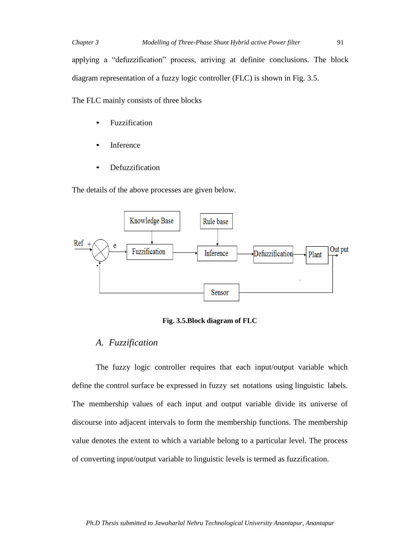
applying a “defuzzification” process, arriving at definite conclusions. The block
diagram representation of a fuzzy logic controller (FLC) is shown in Fig. 3.5.
The FLC mainly consists of three blocks
• Fuzzification
• Inference
• Defuzzification
The details of the above processes are given below.
Fig. 3.5.Block diagram of FLC
A. Fuzzification
The fuzzy logic controller requires that each input/output variable which
define the control surface be expressed in fuzzy set notations using linguistic labels.
The membership values of each input and output variable divide its universe of
discourse into adjacent intervals to form the membership functions. The membership
value denotes the extent to which a variable belong to a particular level. The process
of converting input/output variable to linguistic levels is termed as fuzzification.
Chapter 3 Modelling of Three-Phase Shunt Hybrid active Power filter 92
Ph.D Thesis submitted to Jawaharlal Nehru Technological University Anantapur, Anantapur
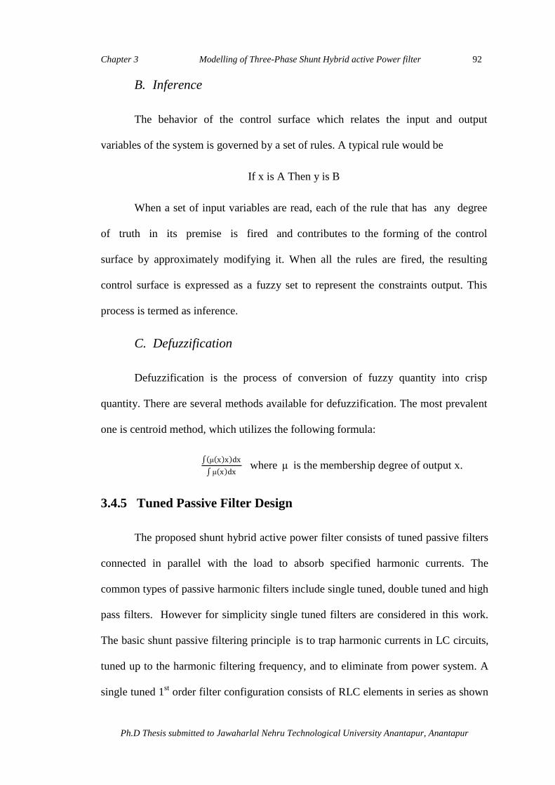
B. Inference
The behavior of the control surface which relates the input and output
variables of the system is governed by a set of rules. A typical rule would be
If x is A Then y is B
When a set of input variables are read, each of the rule that has any degree
of truth in its premise is fired and contributes to the forming of the control
surface by approximately modifying it. When all the rules are fired, the resulting
control surface is expressed as a fuzzy set to represent the constraints output. This
process is termed as inference.
C. Defuzzification
Defuzzification is the process of conversion of fuzzy quantity into crisp
quantity. There are several methods available for defuzzification. The most prevalent
one is centroid method, which utilizes the following formula:
μ x x dx
μ x dx where μ is the membership degree of output x.
3.4.5 Tuned Passive Filter Design
The proposed shunt hybrid active power filter consists of tuned passive filters
connected in parallel with the load to absorb specified harmonic currents. The
common types of passive harmonic filters include single tuned, double tuned and high
pass filters. However for simplicity single tuned filters are considered in this work.
The basic shunt passive filtering principle is to trap harmonic currents in LC circuits,
tuned up to the harmonic filtering frequency, and to eliminate from power system. A
single tuned 1st order filter configuration consists of RLC elements in series as shown
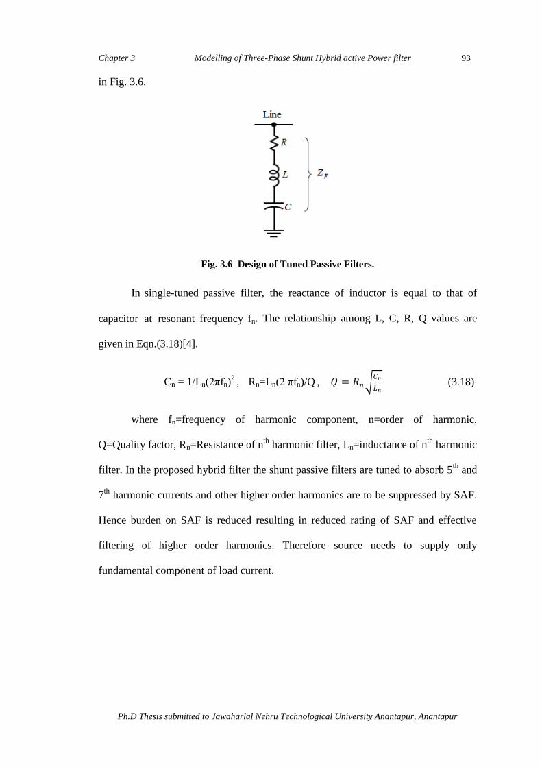
Chapter 3 Modelling of Three-Phase Shunt Hybrid active Power filter 93
Ph.D Thesis submitted to Jawaharlal Nehru Technological University Anantapur, Anantapur
in Fig. 3.6.
Fig. 3.6 Design of Tuned Passive Filters.
In single-tuned passive filter, the reactance of inductor is equal to that of
capacitor at resonant frequency fn. The relationship among L, C, R, Q values are
given in Eqn.(3.18)[4].
Cn = 1/Ln(2πfn)2
,
Rn=Ln(2 πfn)/Q , 𝑄 = 𝑅𝑛
𝐶𝑛
𝐿𝑛 (3.18)
where fn=frequency of harmonic component, n=order of harmonic,
Q=Quality factor, Rn=Resistance of nth
harmonic filter, Ln=inductance of nth
harmonic
filter. In the proposed hybrid filter the shunt passive filters are tuned to absorb 5th
and
7th
harmonic currents and other higher order harmonics are to be suppressed by SAF.
Hence burden on SAF is reduced resulting in reduced rating of SAF and effective
filtering of higher order harmonics. Therefore source needs to supply only
fundamental component of load current.
Chapter 3 Modelling of Three-Phase Shunt Hybrid active Power filter 94
Ph.D Thesis submitted to Jawaharlal Nehru Technological University Anantapur, Anantapur
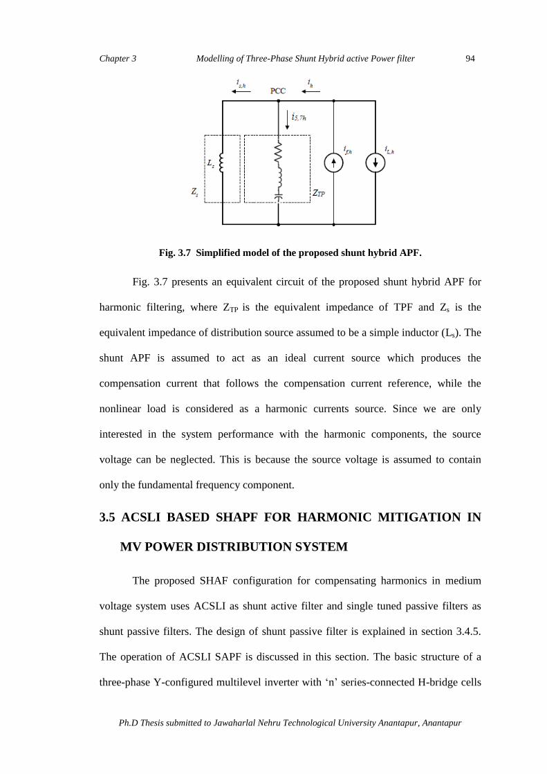
Fig. 3.7 Simplified model of the proposed shunt hybrid APF.
Fig. 3.7 presents an equivalent circuit of the proposed shunt hybrid APF for
harmonic filtering, where ZTP is the equivalent impedance of TPF and Zs is the
equivalent impedance of distribution source assumed to be a simple inductor (Ls). The
shunt APF is assumed to act as an ideal current source which produces the
compensation current that follows the compensation current reference, while the
nonlinear load is considered as a harmonic currents source. Since we are only
interested in the system performance with the harmonic components, the source
voltage can be neglected. This is because the source voltage is assumed to contain
only the fundamental frequency component.
3.5 ACSLI BASED SHAPF FOR HARMONIC MITIGATION IN
MV POWER DISTRIBUTION SYSTEM
The proposed SHAF configuration for compensating harmonics in medium
voltage system uses ACSLI as shunt active filter and single tuned passive filters as
shunt passive filters. The design of shunt passive filter is explained in section 3.4.5.
The operation of ACSLI SAPF is discussed in this section. The basic structure of a
three-phase Y-configured multilevel inverter with „n‟ series-connected H-bridge cells

Chapter 3 Modelling of Three-Phase Shunt Hybrid active Power filter 95
Ph.D Thesis submitted to Jawaharlal Nehru Technological University Anantapur, Anantapur
per phase is shown in Fig. 3.8.
Fig. 3.8 Circuit diagram of a three-phase cascaded multilevel inverter.
A phase voltage waveform is obtained by summing the output voltages of the inverter
cells as in Eqn.(3.19).
Va(t) = Va1(t)+Va2(t)+…..+Van(t) (3.19)
If DC voltage sources of all H-bridge cells are equal, the maximum number of levels
(m) of phase voltage is given by Eqn.(3.20).
m = 2n + 1 (3.20)
On the other hand, if at least one of the DC voltage sources is different of the
other ones, the multilevel inverter can be called as asymmetric multilevel inverter.
Thus, considering the lowest DC voltage source (V1) as base value for the p.u.
notation (Vbase =V1), the normalized values of all DC voltage sources must be natural
numbers to obtain a uniform step multilevel inverter, i.e.:
Vj є N , j = 1, 2, ..., n. Vj=normalized voltage of DC source j. (3.21)

Chapter 3 Modelling of Three-Phase Shunt Hybrid active Power filter 96
Ph.D Thesis submitted to Jawaharlal Nehru Technological University Anantapur, Anantapur
Moreover, to obtain a uniform step multilevel inverter, the DC voltage sources
of the H-bridge cells must also respect the following relation given in Eqn.(3.22):
Vj ≤ 1+2 𝑉𝑘𝑗−1𝑘=1 , 𝑗 = 2,3, …… . . , 𝑛 (3.22)
It is also considered that the DC voltage sources are arranged in an increasing
way as in Eqn.(3.23).
V1≤ V2≤ V3≤ ...≤ Vn (3.23)
Therefore, the maximum number of levels of output phase voltage waveform
can be given by Eqn.(3.24).
M= 2σn + 1 where σn = Vjnj=1 (3.24)
From Eqns.(3.20) and (3.24), it is possible to verify that asymmetric multilevel
inverters can generate a larger number of levels with the same number of cells. Hence
in this thesis asymmetric cascaded inverter with two H-Bridge cells (LV cell and HV
cell) in cascade is used as shunt active power filter for harmonic mitigation in medium
voltage distribution system. On the DC side of HV cell 3kV DC supply is connected
and on LV cell a capacitor is connected as storage device. Fuzzy logic controller is
used for maintaining LV cell capacitor voltage constant. The FLC design is explained
in section 3.4.4.3.
Carrier switching frequency subharmonic PWM is used for producing
switching signals for ACSLI. For m-level inverter this technique uses (m-1) triangular
carrier signals with the same frequency, same peak-to-peak amplitude and same phase
which are disposed such that the bands they occupy are contiguous. The sinusoidal
modulation waveform is centered in the middle of the carrier set and is continuously
compared with each of the carrier signals. If the reference is greater than a carrier
Chapter 3 Modelling of Three-Phase Shunt Hybrid active Power filter 97
Ph.D Thesis submitted to Jawaharlal Nehru Technological University Anantapur, Anantapur
signal, then the active device corresponding to that carrier is switched on, and if the
reference is less than a carrier signal, then the active device corresponding to that
carrier is switched off. This method is also known as sinusoidal pulse width
modulation. D-q-0 theory is used for estimating reference compensating current of
SAPF which is described in section 3.4.4.1.
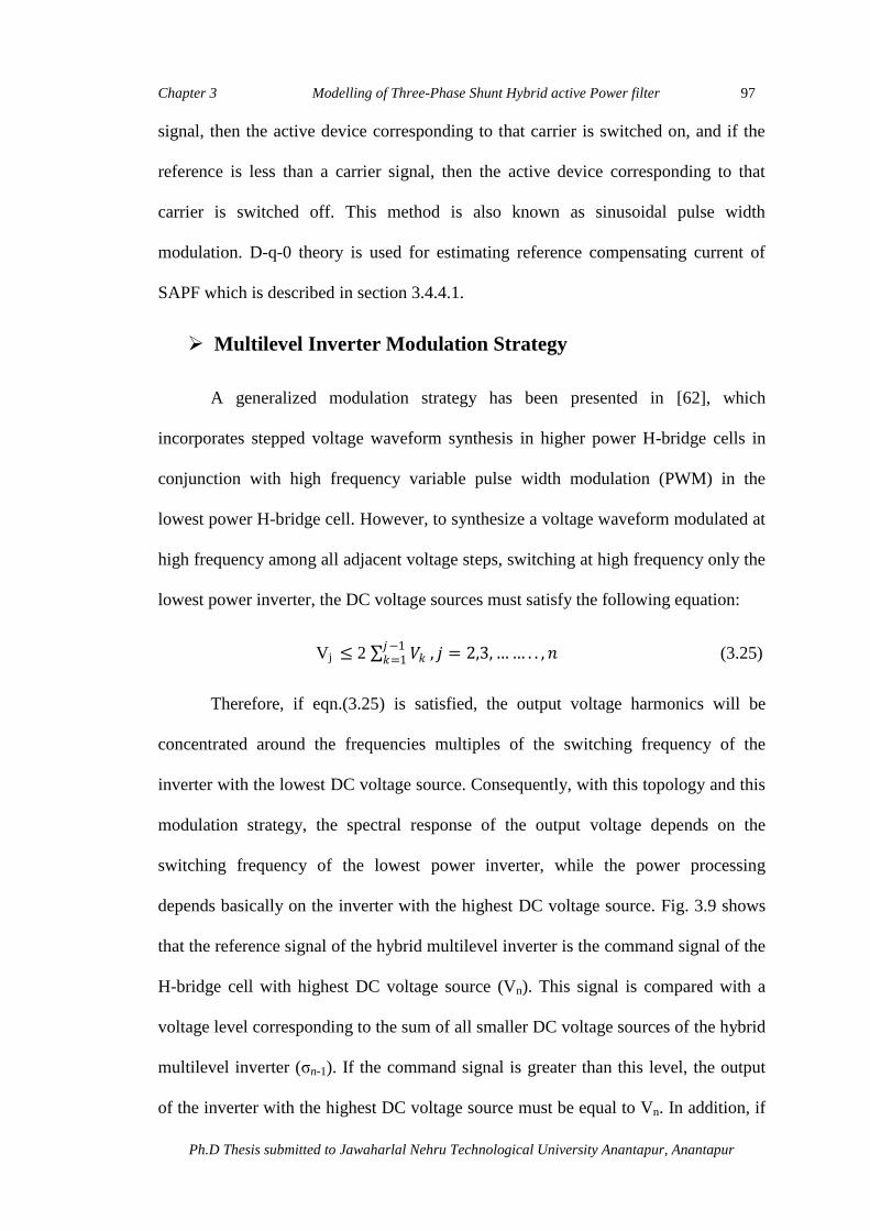
Multilevel Inverter Modulation Strategy
A generalized modulation strategy has been presented in [62], which
incorporates stepped voltage waveform synthesis in higher power H-bridge cells in
conjunction with high frequency variable pulse width modulation (PWM) in the
lowest power H-bridge cell. However, to synthesize a voltage waveform modulated at
high frequency among all adjacent voltage steps, switching at high frequency only the
lowest power inverter, the DC voltage sources must satisfy the following equation:
Vj ≤ 2 𝑉𝑘𝑗−1𝑘=1 , 𝑗 = 2,3, … … . . , 𝑛 (3.25)
Therefore, if eqn.(3.25) is satisfied, the output voltage harmonics will be
concentrated around the frequencies multiples of the switching frequency of the
inverter with the lowest DC voltage source. Consequently, with this topology and this
modulation strategy, the spectral response of the output voltage depends on the
switching frequency of the lowest power inverter, while the power processing
depends basically on the inverter with the highest DC voltage source. Fig. 3.9 shows
that the reference signal of the hybrid multilevel inverter is the command signal of the
H-bridge cell with highest DC voltage source (Vn). This signal is compared with a
voltage level corresponding to the sum of all smaller DC voltage sources of the hybrid
multilevel inverter (σn-1). If the command signal is greater than this level, the output
of the inverter with the highest DC voltage source must be equal to Vn. In addition, if
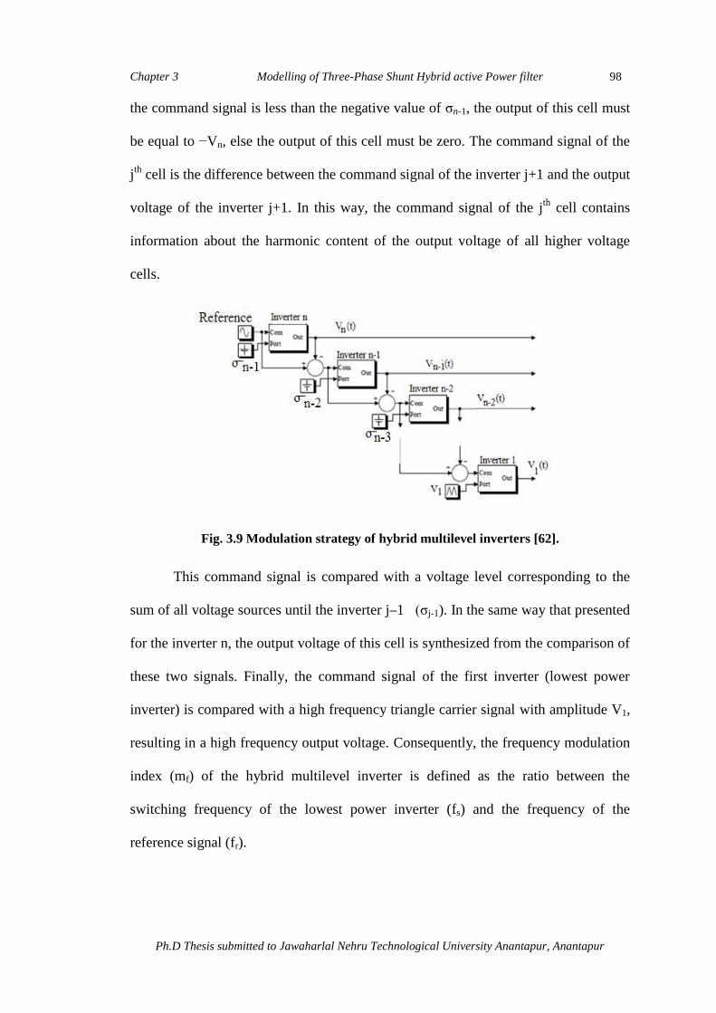
Chapter 3 Modelling of Three-Phase Shunt Hybrid active Power filter 98
Ph.D Thesis submitted to Jawaharlal Nehru Technological University Anantapur, Anantapur
the command signal is less than the negative value of σn-1, the output of this cell must
be equal to −Vn, else the output of this cell must be zero. The command signal of the
jth
cell is the difference between the command signal of the inverter j+1 and the output
voltage of the inverter j+1. In this way, the command signal of the jth
cell contains
information about the harmonic content of the output voltage of all higher voltage
cells.
Fig. 3.9 Modulation strategy of hybrid multilevel inverters [62].
This command signal is compared with a voltage level corresponding to the
sum of all voltage sources until the inverter j–1 (σj-1). In the same way that presented
for the inverter n, the output voltage of this cell is synthesized from the comparison of
these two signals. Finally, the command signal of the first inverter (lowest power
inverter) is compared with a high frequency triangle carrier signal with amplitude V1,
resulting in a high frequency output voltage. Consequently, the frequency modulation
index (mf) of the hybrid multilevel inverter is defined as the ratio between the
switching frequency of the lowest power inverter (fs) and the frequency of the
reference signal (fr).

Chapter 3 Modelling of Three-Phase Shunt Hybrid active Power filter 99
Ph.D Thesis submitted to Jawaharlal Nehru Technological University Anantapur, Anantapur
3.6 CONCLUSION
This chapter explained the principle of operation of proposed SHAF topology
and modelling of basic three phase shunt active filter in detail. The overall topology is
highlighted to give an overview of the work. Then, the design of each main block
namely power source, interfacing inductor and DC bus capacitor followed by tuned
passive filter. It also presented ACSLI based SHAF operation, component design and
its control strategy. A larger number of levels can be obtained with the same number
of power devices of the conventional cascaded multilevel inverter, minimizing the
THD of output voltage with ACSLI.