Embed Size (px)
Citation preview

Modelling of multilayer on-chip transformers
C. Tsui and K.Y. Tong
Abstract: An analytical model has been proposed for multilayer stacked on-chip transformers,including the effects of the eddy current losses in the metal layers and Si substrate. The model givesgood agreement with S-parameter measurements on structures fabricated using a four-metal-layer0.35mm CMOS process. It is shown that proper account of the eddy current losses is necessary topredict accurately the S-parameter characteristics of on-chip transformers at higher frequencies.
1 Introduction
On-chip inductors and transformers in Si CMOS ICs havereceived great attention because of the potential of achievingcompact and cheap SoC systems. On-chip transformers canbe used in baluns, impedance matching, filters and low-voltage mixer applications [1–4]. The transformer can befabricated either on the same metal layer or in multiplelayers. Planar transformers have low mutual magneticcoupling coefficients between windings and occupy largerareas. However, using multiple metal layers can achieve ahigher coupling coefficient and saves area, though at theexpense of higher capacitances between the windings. Dueto the complexity of multilayer transformers, compactmodelling of the transformers is especially valuable inefficient simulation and design of RF circuits. Previousreports [5–7] usually do not include detailed modellingof multilayer transformers, particularly the eddy currentlosses in the metal layers and Si substrate, which wouldbecome significant at higher frequencies. Such losseshave important influences on the performance of trans-formers aimed at delivering powers to loads. In this paper,we shall describe an analytical model of multilayer on-chiptransformers including the eddy current losses in thetransformer.
In our model, each winding on a metal layer isrepresented by its self-inductance, series resistance andinterwinding capacitance, in addition to mutual inductanceswith other windings and interlayer capacitances. A specificfeature of the model is that the series resistance of thewindings include (i) losses due to the proximity effect, i.e.eddy current loss in a metal segment induced by themagnetic flux generated by other segments, and (ii) eddycurrent loss in the Si substrate.
Evaluation of the above losses is needed in the properdetermination of the Q-factor of on-chip inductors. In thiswork, we have extended our previously developed methodof calculating the proximity effect loss and substrate loss ininductors [8] to the case of transformers.
2 Model
2.1 Equivalent circuitTo confirm the validity of our approach to the modelling ofon-chip transformers, we have fabricated and characterisedmultilayer transformers using a four-metal 0.35mm CMOSprocess. The structure is a stacked balun transformer usingmetal 2 and metal 4 as the secondary windings, and metal 3as the primary winding (where metal 4 is the top layer).Each winding on the three metal layers are identical squarespirals. Figure 1a shows the equivalent circuit of the threewindings including the self-inductances, series resistances,interwinding capacitances and interlayer capacitances.(Interwinding capacitance is the capacitance betweenparallel metal segments on the same winding due to thelateral field, and interlayer capacitance is the capacitancebetween metal segments on two different windings, asillustrated in Fig. 1b.) L1 and R1 are the self-inductance andseries resistance of the primary winding P1 on the metal 3layer; L2 and R2 are the self-inductance and series resistanceof the secondary winding P2 on the metal 4 layer; L3 and R3
are the self-inductance and series resistance of the secondarywinding P3 on the metal 2 layer. As in the usual lumpedmodels, the interlayer capacitances are assumed to beequally distributed at the two terminals of a winding. C12 ishalf of the total capacitance between the segments on themetal 3 and metal 4 layers. Similarly C13 is half of the totalcapacitance between the segments on the metal 3 and metal2 layers. Co1, Co2 and Co3 are the interwinding capacitancesfor the P1, P2, and P3 windings, respectively. C3S is half ofthe total capacitance between the segments on the metal 2layer and the Si substrate.
For S-parameter measurement purposes, one terminal ofthe primary winding and the centre tap of the secondarywindings are grounded. Figure 2 shows the equivalentcircuit of the transformer under this condition, where CS
and RS are the substrate capacitance and resistance,respectively. Because of the common grounding betweenthe primary and centre tap of the secondary winding, someof the interlayer capacitances are effectively short-circuited.
The interwinding capacitance is approximately given bythe following equation [9]:
Co1 � lrCL
n� 1þ CBR
2ð1Þ
where CL is the capacitance per unit length between twoparallel metals segment due to the lateral field, lT is the totallength of metal in the winding, n is the number of turns andE-mail: [email protected]
The authors are with the Department of Electronic and Information Engi-neering, The Hong Kong Polytechnic University, Hong Kong, China
r The Institution of Engineering and Technology 2006
IEE Proceedings online no. 20050135
doi:10.1049/ip-map:20050135
Paper first received 5th June and in revised form 30th December 2005
IEE Proc.-Microw. Antennas Propag., Vol. 153, No. 5, October 2006 483

CBR is the capacitance of the bridge connecting the centre ofthe winding to the external port.
The self-inductances are calculated using Greenhouse’smethod [10], which gives more accurate values than otherapproximation methods. For example, the self-inductanceof the primary winding is derived from the summationX
i
Li þX
i;j
dijMij
where Li is the self-inductance of the ith segment on theprimary winding, Mij is the mutual inductance between theith and jth parallel segments on the primary winding and dij
equals +1 or � 1 depending on current direction. Themutual inductance between two windings is deduced fromthe coupling coefficient, which is about 0.9 for stackedtransformers [6].
2.2 Proximity effect and substrate lossesThe series resistance of a winding is equal to
Rshlr
Wþ Rpr þ Rsub
� �
where Rsh is the sheet resistance, lT is the total length ofmetal and W is the width of metal. The eddy current lossesare represented by equivalent resistances in the winding,with Rpr representing the loss due to the proximity effectand Rsub representing the substrate eddy current loss.
In an inductor, Rpr is found from the eddy current lossPed in the metal layer as Rpr ¼ Ped/I
2, where I is theimpressed current. In a transformer, the magnetic fluxgenerated by a winding also induces eddy current losses inother windings. It is convenient to express all the eddycurrent losses as an equivalent resistance in the winding,which is the source of the magnetic flux. Therefore, in atransformer with n windings, Rpr for the ith winding with animpressed current Ii is given by
Rpr ¼Xn
j¼1Ped;j=I2i ð2Þ
where Ped,j is the eddy current loss in the jth winding due tothe magnetic flux generated by the current in the ithwinding. In a multilayer transformer, Ped,j is roughly thesame for different values of j, since the metal layerseparation is much less than the lateral diameters of thewindings. So, in our case, Rpr is about three times the valuewhich would be obtained without considering the lossesinduced by coupling from other windings.
To evaluate Rpr, we need a method of determining theeddy current loss in a metal segment. The eddy current lossin a metal segment can be derived from the magnetic fluxpenetrating the segment due to an impressed current I inother segments [8, 11]. The following approach is based onour previous work developed for an inductor [8]. Theaverage magnetic field Bm at the mth segment is determinedby summing up the fields due to all the other parallel kthsegments
Bm ¼ CX
k
moIdk
4pdk
lkffiffiffiffiffiffiffiffiffiffiffiffiffiffiffiffiffiffiffid2
k þ l2k=4q264
375 ð3Þ
where lk is the length of the kth segment, dk is the distancebetween the centre lines of the mth and kth segments, dk
equals +1 or � 1 depending on the direction of current in
Secondary P2
Secondary P3
Primary P1
Co2
R2 L2
Co1
R1 L1
Co3
R3 L3
C12 C12
C13 C13
C3S C3S
Si substrate
inter-winding capacitance
inter-layer capacitance
Metal 2
Metal 3
a
b
Fig. 1 Equivalent circuit and interwinding and interlayer capaci-tancesa Equivalent circuit of the windingsb Cross-section of metal segments showing interwinding and interlayercapacitances
C12
C13
Co3
L1
L2
L3 R1
R2
R3
Secondary P2
Secondary P3
Co2
Co1
C3S
CS
RS
Primary P1
Fig. 2 Equivalent circuit of the multilayer transformer
484 IEE Proc.-Microw. Antennas Propag., Vol. 153, No. 5, October 2006
the kth segment, and C is a constant used to compensate forthe variation of magnetic field across the mth segment. Chas a value less than one because the magnetic field atthe ends of the centre line is lower than that at the middle.It is well known that the eddy current flows aroundthe edges of the segment. The magnitude of the inducedvoltage vm around the loop due to the magnetic field Bm isgiven by
vm ¼ 2pfBmlm W � 2wedð Þ ð4Þwhere f is the signal frequency and wed is the width of theeddy current at the edges of the segment. We then calculatethe eddy current in the mth segment Ied by consideringthe impedance of the eddy current path including both theresistance red and reactance Led. The eddy current loss inthe mth segment is thus given by I2edred . The above methodof determining the proximity effect losses [8] has beenverified by comparison with numerical simulation andexperimental Q-factor measurements in multilayer inductors.
The eddy current loss in the substrate Psub is determinedin a similar way as in our previous work on inductors [8]
Psub ¼p2A2B2
cf 2tsi8rsi
ð5Þ
where A is area of the transformer, Bc is the magnetic fieldat the centre of the transformer, rsi is the substrate resistivityand tsi is a fitting parameter for the effective penetrationdepth. Equation (7) is derived from the consideration of theeddy current loss due to a uniform magnetic field in thesubstrate equal to the value of Bc. Though the formula issimple, it brings out the important property that the lossincreases as the square of the frequency and is inverselyproportional to the substrate resistivity. For the current ineach winding, values of Bc and Psub are determined asabove, and then used to evaluate the equivalent seriesresistance Rsub in the winding representing the substrateloss.
3 Results and discussions
Each winding on metal 2, metal 3 and metal 4 is identical(Fig. 3), consisting of four turns and an outside diameter of200mm. The top metal 4 layer is thicker and has a lower
sheet resistance of 40mO/square compared to that of80mO/square of the other layers. The width of the metal is10mm and the spacing between two adjacent segments is2mm.
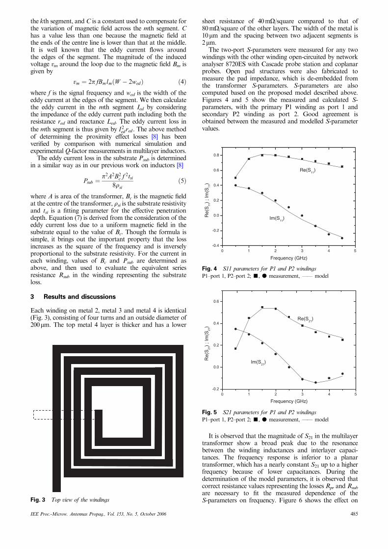
The two-port S-parameters were measured for any twowindings with the other winding open-circuited by networkanalyser 8720ES with Cascade probe station and coplanarprobes. Open pad structures were also fabricated tomeasure the pad impedance, which is de-embedded fromthe transformer S-parameters. S-parameters are alsocomputed based on the proposed model described above.Figures 4 and 5 show the measured and calculated S-parameters, with the primary P1 winding as port 1 andsecondary P2 winding as port 2. Good agreement isobtained between the measured and modelled S-parametervalues.
It is observed that the magnitude of S21 in the multilayertransformer show a broad peak due to the resonancebetween the winding inductances and interlayer capaci-tances. The frequency response is inferior to a planartransformer, which has a nearly constant S21 up to a higherfrequency because of lower capacitances. During thedetermination of the model parameters, it is observed thatcorrect resistance values representing the losses Rpr and Rsub
are necessary to fit the measured dependence of theS-parameters on frequency. Figure 6 shows the effect onFig. 3 Top view of the windings
0 1 2 3 4 5-0.4
-0.2
0.0
0.2
0.4
0.6
0.8
Im(S11
)
Re(S11
)
Re(
S11
) ; I
m(S
11)
Frequency (GHz)
Fig. 4 S11 parameters for P1 and P2 windings
P1–port 1, P2–port 2; ’, � measurement, FF model
0 1 2 3 4 5-0.2
0.0
0.2
0.4
0.6
Im(S21
)
Re(S21
)
Re(
S21
) ; I
m(S
21)
Frequency (GHz)
Fig. 5 S21 parameters for P1 and P2 windings
P1–port 1, P2–port 2; ’, � measurement, FF model
IEE Proc.-Microw. Antennas Propag., Vol. 153, No. 5, October 2006 485
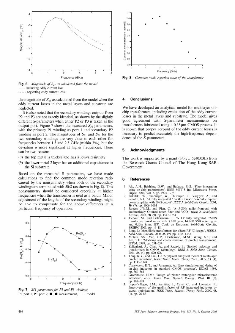
the magnitude of S21 as calculated from the model when theeddy current losses in the metal layers and substrate areneglected.
It is also noted that the secondary windings outputs fromP2 and P3 are not exactly identical, as shown by the slightlydifferent S-parameters when either P2 or P3 is taken as theoutput port. Figure 7 shows the measured S31 parameters,with the primary P1 winding as port 1 and secondary P2winding as port 2. The magnitudes of S21 and S31 for thetwo secondary windings are very close to each other forfrequencies between 1.5 and 2.5 GHz (within 3%), but thedeviation is more significant at higher frequencies. Therecan be two reasons:
(a) the top metal is thicker and has a lower resistivity
(b) the lower metal 2 layer has an additional capacitance tothe Si substrate.
Based on the measured S parameters, we have madecalculations to find the common mode rejection ratiocaused by the nonsymmetry when both of the secondarywindings are terminated with 50O (as shown in Fig. 8). Thisnonsymmetry should be considered especially at higherfrequencies when the transformer is used as a balun. Minoradjustment of the lengths of the secondary windings mightbe able to compensate for the above differences at aparticular frequency of operation.
4 Conclusions
We have developed an analytical model for multilayer on-chip transformers, including evaluation of the eddy currentlosses in the metal layers and substrate. The model givesgood agreement with S-parameter measurements ontransformers fabricated using a 0.35mm CMOS process. Itis shown that proper account of the eddy current losses isnecessary to predict accurately the high-frequency depen-dence of the S-parameters.
5 Acknowledgments
This work is supported by a grant (PolyU 5240/03E) fromthe Research Grants Council of The Hong Kong SARGovernment.
6 References
1 Aly, A.H., Beishline, D.W., and Badawy, E.-S.: ‘Filter integrationusing on-chip transformers’. IEEE MTT-S Int. Microwave Symp.Digest, 2004, Vol. 3, pp. 1975–1978
2 Bakalski, W., Simburger, W., Thuringer, R., Vasylyev, A., andScholtz, A.L.: ‘A fully integrated 5.3-GHz 2.4-V 0.3-W SiGe bipolarpower amplifier with 50-O output’, IEEE J. Solid-State Circuits, 2004,39, (7), pp. 1006–1014
3 Rogers, J.W.M., and Plett, C.: ‘A 5-GHz radio front-end withautomatically Q-tuned notch filter and VCO’, IEEE J. Solid-StateCircuits, 2003, 38, (9), pp. 1547–1554
4 Tiebout, M., and Liebermann, T.: ‘A 1V fully integrated CMOStransformer based mixer with 5.5dB gain, 14.5dB SSB noise figureand 0dBm input IP3’. Conf. on European Solid-State Circuits,ESSIRC 2003, pp. 16–18
5 Long, J.: ‘Monolithic transformers for silicon RF IC design,’, IEEE J.Solid-State Circuits, 2000, 35, (9), pp. 1368–1382
6 Mohan, S.S., Yue, C.P., Hershenson, M.M., Wong, S.S., andLee, T.H.: ‘Modeling and characterization of on-chip transformers’.IEDM, 1998, pp. 531–534
7 Zolfaghari, A., Chan, A., and Razavi, B.: ‘Stacked inductors andtransformers in CMOS technology’, IEEE J. Solid State Circuits,2001, 36, (4), pp. 620–628
8 Tong, K.Y., and Tsui, C.: ‘A physical analytical model of multi-layeron-chip inductors’, IEEE Trans. Micro. Theory Tech., 2005, 53, (4),pp. 1143–1149
9 Christensen, K.T., and Jorgensen, A.: ‘Easy simulation and design ofon-chip inductors in standard CMOS processes’. ISCAS 1998,pp. 360–364
10 Greenhouse, H.M.: ‘Design of planar rectangular microelectronicinductors’, IEEE Trans. Parts Hybrids Packag., 1974, 10, (2),pp. 101–109
11 Lopez-Villegas, J.M., Samitier, J., Cane, C., and Losantos, P.:‘Improvement of the quality factor of RF integrated inductors bylayout optimization’, IEEE Trans. Microw. Theory Tech., 2000, 48,(1), pp. 76–83
0 1 2 3 4 5-14
-12
-10
-8
-6
-4
Mag
nitu
de o
f S21
(dB
)
Frequency (GHz)
Fig. 6 Magnitude of S21 as calculated from the modelFF including eddy current loss- - - - - neglecting eddy current loss
0 1 2 3 4 5-0.2
0.0
0.2
0.4
0.6
Im(S31
)
Re(S31
)
Re(
S31
) ; I
m(S
31)
Frequency (GHz)
Fig. 7 S31 parameters for P1 and P3 windings
P1–port 1, P3–port 2; ’,� measurement, FF model
0 1 2 3 4 528
29
30
31
32
33
34
35
36
37
Com
mon
mod
e re
ject
ion
ratio
(dB
)
Frequency (GHz)
Fig. 8 Common mode rejection ratio of the transformer
486 IEE Proc.-Microw. Antennas Propag., Vol. 153, No. 5, October 2006
![(MLV) MULTILAYER CHIP VARISTOR - fenghua.comfenghua.com/pdf/varistor/chip_varistor.pdf · (MLV) MULTILAYER CHIP VARISTOR Multilayer Chip ... [2220] 8063[3225] 1080[4032] 55 125 V](https://img.pdfslide.us/doc/110x75/5b42af3a7f8b9ad23b8b5240/mlv-multilayer-chip-varistor-mlv-multilayer-chip-varistor-multilayer-chip.jpg)


![BLF881; BLF881S · C1, C2 multilayer ceramic chip capacitor 5.1 pF [1] C3, C4 multilayer ceramic chip capacitor 10 pF [2] C5 multilayer ceramic chip capacitor 6.8 pF [1] C6 multilayer](https://img.pdfslide.us/doc/110x75/5ceec0d888c99376408beb1c/blf881-blf881s-c1-c2-multilayer-ceramic-chip-capacitor-51-pf-1-c3-c4-multilayer.jpg)