Embed Size (px)
Citation preview
Accepted Manuscript
Modeling Tools For Design Of Type-II Superlattice Photodetectors
Carl Asplund, Rickard Marcks von Würtemberg, Linda Höglund
PII: S1350-4495(16)30583-7
DOI: http://dx.doi.org/10.1016/j.infrared.2017.03.006
Reference: INFPHY 2255
To appear in: Infrared Physics & Technology
Received Date: 26 October 2016
Revised Date: 28 February 2017
Accepted Date: 8 March 2017
Please cite this article as: C. Asplund, R. Marcks von Würtemberg, L. Höglund, Modeling Tools For Design Of
Type-II Superlattice Photodetectors, Infrared Physics & Technology (2017), doi: http://dx.doi.org/10.1016/
j.infrared.2017.03.006
This is a PDF file of an unedited manuscript that has been accepted for publication. As a service to our customers
we are providing this early version of the manuscript. The manuscript will undergo copyediting, typesetting, and
review of the resulting proof before it is published in its final form. Please note that during the production process
errors may be discovered which could affect the content, and all legal disclaimers that apply to the journal pertain.
Modeling Tools For Design Of Type-II Superlattice
Photodetectors
Carl Asplund, Rickard Marcks von Würtemberg and Linda Höglund
IRnova AB, Isafjordsgatan 22 C5, SE-164 40 Kista, Sweden
Abstract
In this paper, we present a range of modeling tools that are used in the design and
performance evaluation of type-II superlattice detectors. Among these is an optical and photo
carrier transport model for the spectral total external QE, which takes into account carrier
diffusion length. Using this model, the diffusion length is extracted from external quantum
efficiency measurements. It can also be used to fine-tune an optical cavity in relation to the
wavelength range of interest for optimal quantum efficiency. Furthermore, an electrical
device model for band bending, dark current and doping optimization is described. The
modeling tools are discussed and examples of their use are given for MWIR type-II detectors
based on InAs/AlSb/GaSb superlattices.
Keywords: Semiconductor device modeling, electrical simulation, type-II superlattice, SLS,
infrared detector, InAs/GaSb superlattice, MWIR photodetector, doping, quantum efficiency,
numerical precision, carrier diffusion

2
1. INTRODUCTION
Type-II superlattices (T2SLs) are competing with traditional state-of-the-art technologies as a
material of choice for high end infrared (IR) detectors. Good detector performance has been
demonstrated for single pixel detectors as well as focal plane arrays [1], and since a few years back
several companies are offering mid wave (MW) and long wave (LW) detectors based on T2SLs [2].
The performance of homojunction T2SL detectors based on InAs/GaSb is limited by dark current
generation via mid-gap levels. [3] For this reason, heterojunction diode designs are often used,
where most, or all, of the depletion region resides in a higher bandgap material than that of the
absorber. Doping schemes and superlattice band levels in these designs are carefully tuned to
minimize dark current generation, while at the same time allowing photo generated carriers to flow
unimpeded to the contacts. Furthermore, for practical reasons, the epitaxially grown T2SL structures
cannot be made arbitrarily thick. Therefore the absorption and photocurrent generation takes place in
a relatively thin region, compared to competing technologies, such as InSb and HgCdTe (MCT). In
certain applications it is therefore necessary to give some consideration to the optical cavity, in order
to optimize the quantum efficiency for the wavelength range of interest.
To accomplish all these things, and to evaluate the merits of such designs, modeling tools are used.
In this paper we present a range of modeling tools that are used in the design of MW and LW T2SL
detectors based on the InAs/AlSb/GaSb materials system.
2. EXPERIMENTAL
The detector structures were grown on 3-inch n-type (Te-doped) GaSb (100) substrates using solid
source molecular beam epitaxy (MBE). The structures are based on a double heterostructure design
[4] with a large band gap n-type SL contact layer, a lightly doped InAs/GaSb/AlSb/GaSb hole
barrier (hB), a p-type InAs/GaSb SL absorber, a 0.1 µm thick p-type InAs/GaSb electron barrier

3
(eB) and finally a 0.1 µm bulk p-type GaSb layer; see Fig. 1. Single pixel detectors (170 µm × 170
µm) and FPAs with 320x256 pixels and 30 µm pixel pitch are routinely fabricated from this detector
material. To fabricate the FPAs, standard III/V processing techniques are used. [5] The arrays are
then hybridized either to read out circuits or to fan-out chips, underfill is deposited, the GaSb
substrate is fully removed and finally an antireflection (AR) coating is applied. External quantum
efficiency is measured from the backside with fully removed substrate and with the top of pixel
covered by reflecting metal, i.e. a double-pass configuration.
Fig. 1. Band edge diagram of the generic photodiode design that is common for all examples in this
paper. Light enters from the left in the figure through an antireflective coating. The indium bump
and read-out circuit chip is on the right.
3. SUPERLATTICE BAND STRUCTURE CALCULATIONS
A transfer-matrix 8×8 band k⋅P envelope function approximation (EFA) model was used to calculate
the electron band structure.[6],[7],[8] The model can handle an arbitrary number of layers per
superlattice period, and fractions of an InSb monolayer are added at the interfaces to obtain zero
average lattice mismatch in each period. The band structure calculations provide input data for the
electrical model, such as band edge energies and effective masses. It can also be used to obtain
absorption coefficient spectra and tunneling coefficients, as discussed in ref. [9].
4
4. EXTERNAL QE MODEL WITH OPTICAL CAVITY EFFECTS AND PHOTO
CARRIER TRANSPORT
The external QE (EQE) spectrum of the photodetector was calculated using a model that consists of
two parts: The first part calculates the absorption A(z, λ) as a function of position and wavelength,
and the second part solves the diffusion equation using this absorption as source term – in essence
taking into account the probability for the photo generated carriers to reach the p-n junction. The
spatially resolved absorption spectrum at position z is defined as
( )( )
( )λλ
λ ,0,
, Sz
zSzA
∂
∂−≡ ,
where ⟨S(z, λ)⟩ is the time-averaged Poynting vector at z, and ⟨S(0, λ)⟩ is the optical power density
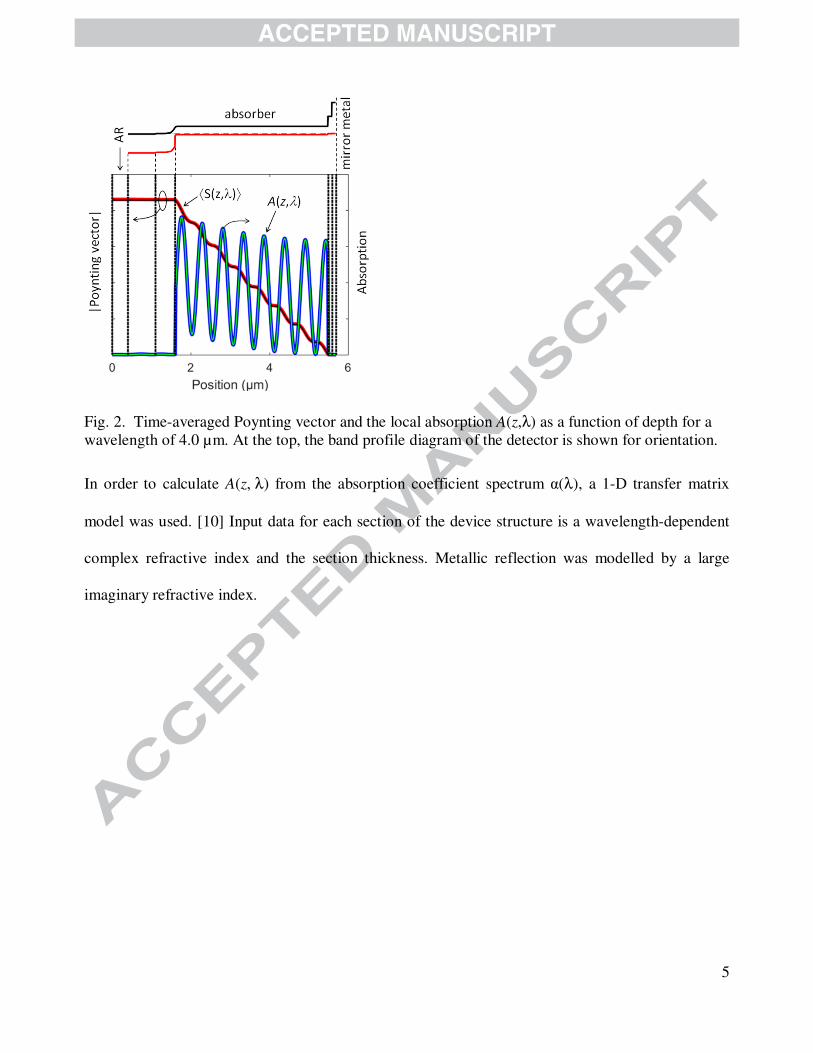
entering the device. These concepts are illustrated in Fig. 2. At the top, the band profile diagram is
shown for orientation. The photon energy λ/hcE = chosen here is larger than the absorber SL
bandgap, but smaller than the bandgaps of the rest of the epi structure. Therefore, the simulated
energy flux decreases visibly only within the absorber. The oscillations in the absorption are caused
by reflection at the mirror metal.
5
Fig. 2. Time-averaged Poynting vector and the local absorption A(z,λ) as a function of depth for a
wavelength of 4.0 µm. At the top, the band profile diagram of the detector is shown for orientation.
In order to calculate A(z, λ) from the absorption coefficient spectrum α(λ), a 1-D transfer matrix
model was used. [10] Input data for each section of the device structure is a wavelength-dependent
complex refractive index and the section thickness. Metallic reflection was modelled by a large
imaginary refractive index.
6
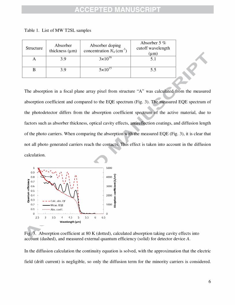
Table 1. List of MW T2SL samples
Structure Absorber
thickness (µm)
Absorber doping
concentration NA (cm-3
)
Absorber 5 %
cutoff wavelength
(µm)
A 3.9 3×10¹⁶
5.1
B 3.9 5×10¹⁵
5.5
The absorption in a focal plane array pixel from structure “A” was calculated from the measured
absorption coefficient and compared to the EQE spectrum (Fig. 3). The measured EQE spectrum of
the photodetector differs from the absorption coefficient spectrum of the active material, due to
factors such as absorber thickness, optical cavity effects, antireflection coatings, and diffusion length
of the photo carriers. When comparing the absorption with the measured EQE (Fig. 3), it is clear that
not all photo generated carriers reach the contacts. This effect is taken into account in the diffusion
calculation.
Fig. 3. Absorption coefficient at 80 K (dotted), calculated absorption taking cavity effects into
account (dashed), and measured external quantum efficiency (solid) for detector device A.
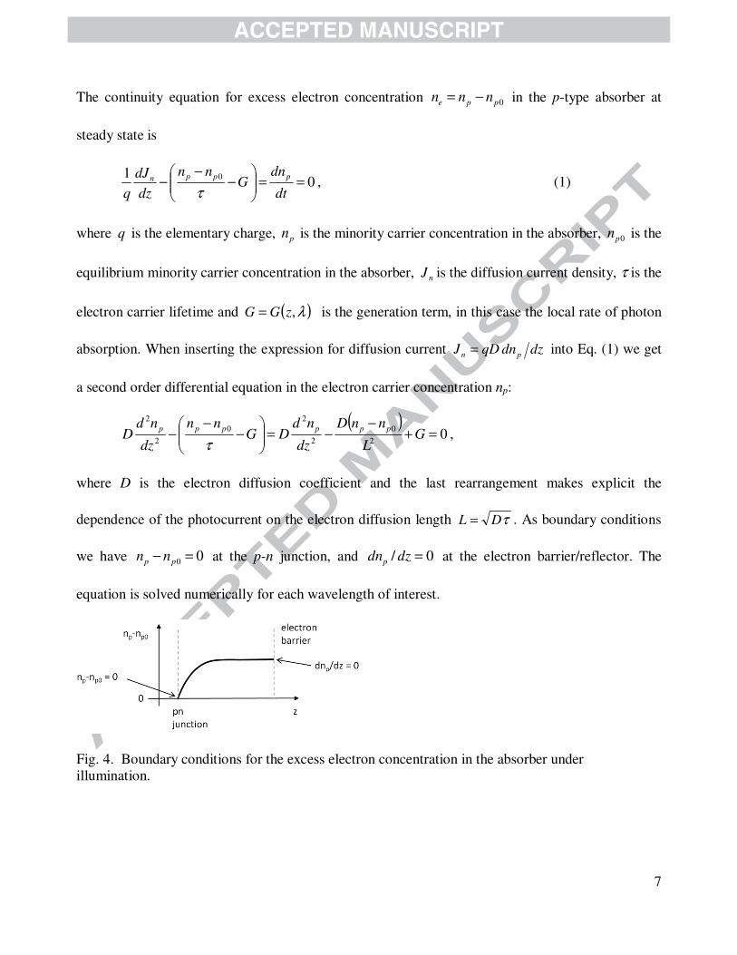
In the diffusion calculation the continuity equation is solved, with the approximation that the electric
field (drift current) is negligible, so only the diffusion term for the minority carriers is considered.
7
The continuity equation for excess electron concentration 0ppe nnn −= in the p-type absorber at
steady state is
,01 0
==
−
−−
dt
dnG
nn
dz
dJ
q
pppn
τ (1)
where q is the elementary charge, pn is the minority carrier concentration in the absorber, 0pn is the
equilibrium minority carrier concentration in the absorber, nJ is the diffusion current density, τ is the
electron carrier lifetime and ( )λ,zGG = is the generation term, in this case the local rate of photon
absorption. When inserting the expression for diffusion current dzdnqDJpn
= into Eq. (1) we get
a second order differential equation in the electron carrier concentration np:
( )
,02
0
2
2
0
2
2
=+−
−=
−
−− G
L
nnD
dz
ndDG
nn
dz
ndD
pppppp
τ
where D is the electron diffusion coefficient and the last rearrangement makes explicit the
dependence of the photocurrent on the electron diffusion length τDL = . As boundary conditions
we have 00 =− pp nn at the p-n junction, and 0/ =dzdnp at the electron barrier/reflector. The
equation is solved numerically for each wavelength of interest.
Fig. 4. Boundary conditions for the excess electron concentration in the absorber under
illumination.
8
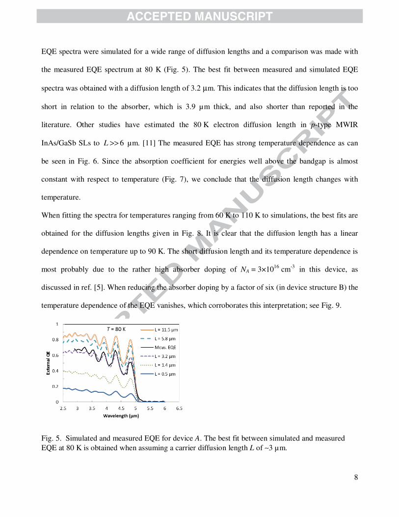
EQE spectra were simulated for a wide range of diffusion lengths and a comparison was made with
the measured EQE spectrum at 80 K (Fig. 5). The best fit between measured and simulated EQE
spectra was obtained with a diffusion length of 3.2 µm. This indicates that the diffusion length is too
short in relation to the absorber, which is 3.9 µm thick, and also shorter than reported in the
literature. Other studies have estimated the 80 K electron diffusion length in p-type MWIR
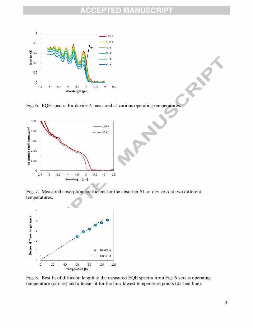
InAs/GaSb SLs to 6>>L µm. [11] The measured EQE has strong temperature dependence as can
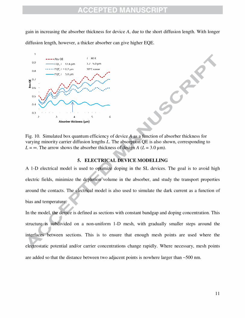
be seen in Fig. 6. Since the absorption coefficient for energies well above the bandgap is almost
constant with respect to temperature (Fig. 7), we conclude that the diffusion length changes with
temperature.
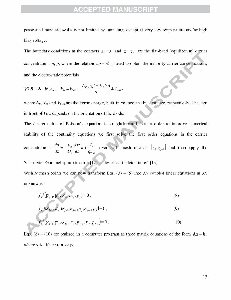
When fitting the spectra for temperatures ranging from 60 K to 110 K to simulations, the best fits are
obtained for the diffusion lengths given in Fig. 8. It is clear that the diffusion length has a linear
dependence on temperature up to 90 K. The short diffusion length and its temperature dependence is
most probably due to the rather high absorber doping of NA = 3×10¹⁶
cm-3
in this device, as
discussed in ref. [5]. When reducing the absorber doping by a factor of six (in device structure B) the
temperature dependence of the EQE vanishes, which corroborates this interpretation; see Fig. 9.
Fig. 5. Simulated and measured EQE for device A. The best fit between simulated and measured
EQE at 80 K is obtained when assuming a carrier diffusion length L of ∼3 µm.
9
Fig. 6. EQE spectra for device A measured at various operating temperatures.
Fig. 7. Measured absorption coefficient for the absorber SL of device A at two different
temperatures.
Fig. 8. Best fit of diffusion length to the measured EQE spectra from Fig. 6 versus operating
temperature (circles) and a linear fit for the four lowest temperature points (dashed line).

10
Fig. 9. Measured EQE at 4 µm wavelength versus temperature for device A with NA = 3×10
16 cm
-3
p-type absorber doping (circles) and device B with NA = 0.5×10¹⁶
cm-3
absorber doping (triangles).
The latter device shows no temperature dependence over the investigated range.
In comparison to the LW window, the number of photons from a room-temperature scene in the
3-5 µm MW transmission window is much smaller, and falls rapidly with decreasing cutoff WL. The
total irradiance (photons/s) from a 30°C scene decreases by almost 20% per 0.1 µm reduction in
cutoff wavelength. It can therefore be advantageous to make the most of the absorption close to the
cutoff energy in order to optimize the detector performance. Consider a cold bandpass filter which
limits the spectral irradiance Eq,λ(λ) from a blackbody of temperature Tscene to the wavelength
interval [a, b]. The photons are absorbed by a detector with quantum efficiency spectrum η(λ). We
define ‘Box QE’, or Boxη , of the detector as the result of weighting the QE spectrum with the
irradiance spectrum over the cold bandpass filter wavelength interval [a,b]:
( ) ( ) ( )∫∫=b
aq
b
aqBox dEdE λλλλληη λλ ,, . (2)
The Box QE can easily be converted into photocurrent by multiplying with the irradiance. Box EQE
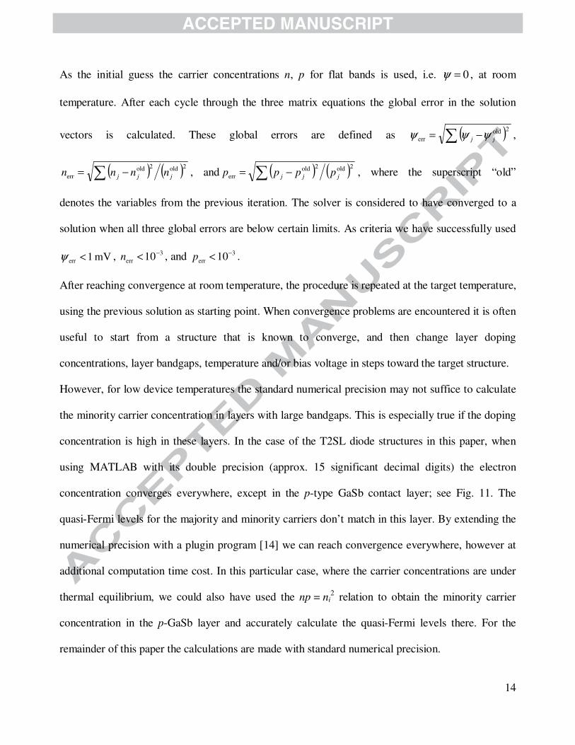
versus absorber thickness curves were calculated for a range of carrier diffusion lengths (Fig. 10).
As the cavity thickness changes, the standing wave peaks move and the strongly wavelength-
dependent weighting in Eq. (2) creates undulations. This simulation shows that there is really no
11
gain in increasing the absorber thickness for device A, due to the short diffusion length. With longer
diffusion length, however, a thicker absorber can give higher EQE.
Fig. 10. Simulated box quantum efficiency of device A as a function of absorber thickness for
varying minority carrier diffusion lengths L. The absorption QE is also shown, corresponding to
L = ∞. The arrow shows the absorber thickness of design A (L = 3.0 µm).
5. ELECTRICAL DEVICE MODELLING
A 1-D electrical model is used to optimize doping in the SL devices. The goal is to avoid high
electric fields, minimize the depletion volume in the absorber, and study the transport properties
around the contacts. The electrical model is also used to simulate the dark current as a function of
bias and temperature.
In the model, the device is defined as sections with constant bandgap and doping concentration. This
structure is subdivided on a non-uniform 1-D mesh, with gradually smaller steps around the
interfaces between sections. This is to ensure that enough mesh points are used where the
electrostatic potential and/or carrier concentrations change rapidly. Where necessary, mesh points
are added so that the distance between two adjacent points is nowhere larger than ∼500 nm.

12
The equations to be solved are the Poisson equation, and the continuity equations for electrons and
holes:
( )−+ −−−−= AD NNnpq
dz
d
ε
ψ2
2
, (3)
( )GRqdz
dJn −= , (4)
( )GRqdz
dJ p −−= , (5)
where
−−=
dz
dnDn
dz
dqJ nnn
ψµ and
+−=
dz
dpDp
dz
dqJ ppp
ψµ are the current relations and
( )pnfGR ,=− are the generation-recombination rate terms. The two main contributions are from
radiative and Shockley-Read-Hall processes:
( ) ( )2
radiative innpBGR −=− , (6)
and
( )( ) ( )
tntp
i
ppnn
nnpGR
+++
−=−
00
2
SRHττ
, (7)
where
−=
−=
Tk
EENp
Tk
EENn
B
tvvt
B
ctct
exp,exp ,
where Et is the trap level in the bandgap, Nc and Nv are the conduction- and valence-band effective
densities of states and B is the radiative recombination coefficient in units of cm3
s-1
. Auger and
tunneling processes are not included in the electrical model. The Auger generation rate is very low
in T2SL and in our experience the performance of heterojunction MW detectors with well-
13
passivated mesa sidewalls is not limited by tunneling, except at very low temperature and/or high
bias voltage.
The boundary conditions at the contacts 0=z and Nzz = are the flat-band (equilibrium) carrier
concentrations n, p, where the relation 2
innp = is used to obtain the minority carrier concentrations,
and the electrostatic potentials
biasFNF
biasbiN Vq
EzEVVz ±
−=±==
)0()()(,0)0( ψψ ,
where EF, Vbi and Vbias are the Fermi energy, built-in voltage and bias voltage, respectively. The sign
in front of Vbias depends on the orientation of the diode.
The discretization of Poisson’s equation is straightforward, but in order to improve numerical
stability of the continuity equations we first solve the first order equations in the carrier
concentrations n
n
n
n
qD
Jn
dz
d
Ddz
dn+−=
ψµ over each mesh interval [ ]1, +jj
zz and then apply the
Scharfetter-Gummel approximation [12] as described in detail in ref. [13].
With N mesh points we can now transform Eqs. (3) – (5) into 3N coupled linear equations in 3N
unknowns:
( ) 0,,,, 11 =+− jjjjj
jpnf ψψψψ , (8)
( ) 0,,,,,, 1111 =+−+− jjjjjjj
j
n pnnnf ψψψ , (9)
( ) 0,,,,,, 1111 =+−+− jjjjjjj
j
p pppnf ψψψ . (10)
Eqs. (8) – (10) are realized in a computer program as three matrix equations of the form bAx = ,
where x is either ψψψψ, n, or p.
14
As the initial guess the carrier concentrations n, p for flat bands is used, i.e. 0=ψ , at room
temperature. After each cycle through the three matrix equations the global error in the solution
vectors is calculated. These global errors are defined as ( )∑ −=2old
err jj ψψψ ,
( ) ( )∑ −=2old2old
err jjj nnnn , and ( ) ( )∑ −=2old2old
err jjj pppp , where the superscript “old”
denotes the variables from the previous iteration. The solver is considered to have converged to a
solution when all three global errors are below certain limits. As criteria we have successfully used
mV1err <ψ , 3
err10−<n , and 3
err10−<p .
After reaching convergence at room temperature, the procedure is repeated at the target temperature,
using the previous solution as starting point. When convergence problems are encountered it is often
useful to start from a structure that is known to converge, and then change layer doping
concentrations, layer bandgaps, temperature and/or bias voltage in steps toward the target structure.
However, for low device temperatures the standard numerical precision may not suffice to calculate
the minority carrier concentration in layers with large bandgaps. This is especially true if the doping
concentration is high in these layers. In the case of the T2SL diode structures in this paper, when
using MATLAB with its double precision (approx. 15 significant decimal digits) the electron
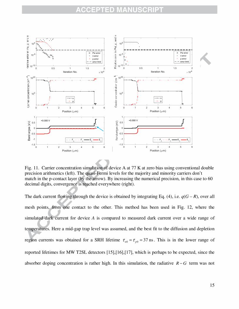
concentration converges everywhere, except in the p-type GaSb contact layer; see Fig. 11. The
quasi-Fermi levels for the majority and minority carriers don’t match in this layer. By extending the
numerical precision with a plugin program [14] we can reach convergence everywhere, however at
additional computation time cost. In this particular case, where the carrier concentrations are under
thermal equilibrium, we could also have used the np = ni2 relation to obtain the minority carrier
concentration in the p-GaSb layer and accurately calculate the quasi-Fermi levels there. For the
remainder of this paper the calculations are made with standard numerical precision.
15
Fig. 11. Carrier concentration simulation of device A at 77 K at zero bias using conventional double precision arithmetics (left). The quasi-Fermi levels for the majority and minority carriers don’t
match in the p-contact layer (by the arrow). By increasing the numerical precision, in this case to 60 decimal digits, convergence is reached everywhere (right).
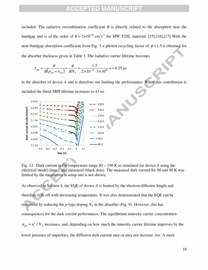
The dark current flowing through the device is obtained by integrating Eq. (4), i.e. q(G – R), over all
mesh points, from one contact to the other. This method has been used in Fig. 12, where the
simulated dark current for device A is compared to measured dark current over a wide range of
temperatures. Here a mid-gap trap level was assumed, and the best fit to the diffusion and depletion
region currents was obtained for a SRH lifetime ns3700
==pn
ττ . This is in the lower range of
reported lifetimes for MW T2SL detectors [15],[16],[17], which is perhaps to be expected, since the
absorber doping concentration is rather high. In this simulation, the radiative GR − term was not
0 0.5 1 1.5 2
Iteration No. 104
10-10
10-5
100
Psi error
n error
p error
error limit
0 1 2 3 4 5 6
Position ( m)
-1.5
-1
-0.5
0
0.5
1
+0.000 V
Fc
Fv
Ec
Ev
0 1 2 3 4 5 6
Position ( m)
100
1020
n
p
0 0.5 1 1.5 2
Iteration No. 104
10-10
10-5
100
Psi error
n error
p error
error limit
0 1 2 3 4 5 6
Position ( m)
-1.5
-1
-0.5
0
0.5
1
+0.000 V
Fc
Fv
Ec
Ev
0 1 2 3 4 5 6
Position ( m)
100
1020
n
p
16
included. The radiative recombination coefficient B is directly related to the absorption near the
bandgap and is of the order of B = 2×10⁻¹⁰
cm3s
-1 for MW T2SL material. [15],[16],[17] With the
near-bandgap absorption coefficient from Fig. 3 a photon recycling factor of 5.1≈φ is obtained for
the absorber thickness given in Table 1. The radiative carrier lifetime becomes
( ) µs25.0s103102
5.11610
00
rad =×⋅×
=≈+
=−
App BNnpB
φφτ
in the absorber of device A and is therefore not limiting the performance. When this contribution is
included the fitted SRH lifetime increases to 43 ns.
Fig. 12. Dark current in the temperature range 80 – 150 K as simulated for device A using the
electrical model (lines), and measured (black dots). The measured dark current for 80 and 90 K was
limited by the measurement setup and is not shown.
As observed in Section 4, the EQE of device A is limited by the electron diffusion length and
therefore falls off with decreasing temperature. It was also demonstrated that the EQE can be
recovered by reducing the p-type doping NA in the absorber (Fig. 9). However, this has
consequences for the dark current performance. The equilibrium minority carrier concentration
Aip Nnn /2
0 ≈ increases, and, depending on how much the minority carrier lifetime improves by the
lower presence of impurities, the diffusion dark current may or may not increase, too. A more
17
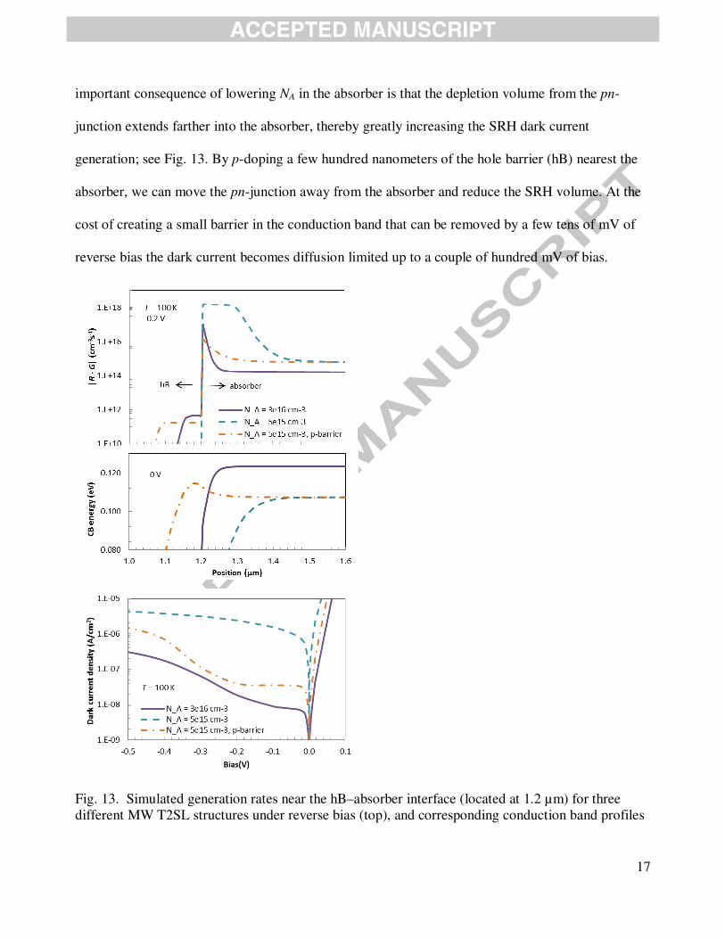
important consequence of lowering NA in the absorber is that the depletion volume from the pn-
junction extends farther into the absorber, thereby greatly increasing the SRH dark current
generation; see Fig. 13. By p-doping a few hundred nanometers of the hole barrier (hB) nearest the
absorber, we can move the pn-junction away from the absorber and reduce the SRH volume. At the
cost of creating a small barrier in the conduction band that can be removed by a few tens of mV of
reverse bias the dark current becomes diffusion limited up to a couple of hundred mV of bias.
Fig. 13. Simulated generation rates near the hB–absorber interface (located at 1.2 µm) for three
different MW T2SL structures under reverse bias (top), and corresponding conduction band profiles

18
at zero bias (middle). The calculated dark currents are shown in the bottom plot. “N_A” is the absorber doping concentration. “N_A = 3e16 cm-3” corresponds to device A.
6. CONCLUSION
The external quantum efficiency (EQE) and dark current of type-II superlattice detectors has been
modeled and compared to measured data. It was found that the EQE in in one of the MW devices
(device A) is limited by the diffusion length, which increases from 2.4 µm at 60 K to 4.1 µm at
110 K. This leads to a strong temperature dependence of the EQE. A reduction of the absorber
doping from NA = 3×1016 cm-3 to 0.5×1016 cm-3 increases the diffusion length so that the EQE
becomes temperature independent, but it also leads to higher dark current. Band edge profile
modeling and dark current calculations suggest how the doping scheme can be modified to mitigate
this effect.
[1] D. Ting, A. Soibel, L. Höglund, J. Nguyen, C. Hill, A. Khoshakhlagh, S.D. Gunapala,
[Semiconductors and Semimetals], “Adv. Infrared Photodetect.“ 84 , 1–57 (2011).
[2] AIM (www.aim-ir.com), IRnova (www.ir-nova.se), SCD (www.scd.co.il), Qmagic
(www.qmagic.com)
[3] J. Pellegrino, R. DeWames, “Minority Carrier Lifetime Characteristics in Type II InAs/GaSb
LWIR Superlattice n+πp+ Photodiodes”, Proc. of SPIE, 7298, 72981U (2009)
[4] D. Ting, C. Hill, A. Soibel, S. Keo, J. Mumolo, J. Nguyen, S.D. Gunapala, “A high-performance
long wavelength superlattice complementary barrier infrared detector”, Appl. Phys. Lett. 95, 023508
(2009)
[5] L. Höglund, C. Asplund, R. Marcks von Würtemberg, H. Kataria, A. Gamfeldt, S. Smuk, H.
Martijn and E. Costard, “Manufacturability of type-II InAs/GaSb superlattice detectors for infrared
imaging”, Infrared Phys. Technol., (submitted) (2017)
19
[6] F. Szmulowicz, H. Haugan, and G. J. Brown, “Effect of interfaces and the spin-orbit band on the
band gaps of InAs/GaSb superlattices beyond the standard envelope-function approximation”, Phys.
Rev. B 69, 155321 (2004)
[7] F. Szmulowicz, “Numerically stable secular equation for superlattices via transfer-matrix
formalism and application to InAs/In0.23Ga0.77Sb and InAs/In0.3Ga0.7Sb/GaSb superlattices”,
Phys. Rev. B 57, 9081 (1998)
[8] F. Szmulowicz, “Solution to spurious bands and spurious real solutions in the envelope-function
approximation”, Phys. Rev. B 71, 245117 (2005)
[9] C. Asplund, R. Marcks von Würtemberg, D. Lantz, H. Malm, H. Martijn, E. Plis, N. Gautam, S.
Krishna, ”Performance of mid-wave T2SL detectors with heterojunction barriers”, Infrared Phys.
Technol. 59, 22-27 (2013)
[10] Max Born, Emil Wolf, “Principles of Optics”, 4th Edition, Pergamon Press, Oxford, 1970
[11] R. Rehm, M. Walther, J. Schmitz, F. Rutz, J. Fleißner, R. Scheibner, J. Ziegler, “InAs/GaSb
superlattices for advanced infrared focal plane arrays”, Infrared Phys. Technol. 52, 344–347 (2009)
[12] D. L. Scharfetter and D. L. Gummel, “Large signal analysis of a Silicon Read diode
oscillator”, IEEE Transaction on Electron Devices, Vol. ED-16, pp.64-77 (1969)
[13] Siegfried Selberherr, “Analysis and Simulation of Semiconductor Devices”, Springer-Verlag
Wien-New York, 1984
[14] “Multiprecision Computing Toolbox for MATLAB” from Advanpix Inc.
(http://www.advanpix.com/)
[15] D. Donetsky, S. Svensson, L. Vorobjev, and G. Belenky, “Carrier lifetime measurements in
short-period InAs/GaSb strained-layer superlattice structures”, Appl. Phys. Lett. 95, 212104 (2009)
20
[16] D. Donetsky, G. Belenky, S. Svensson, and S. Suchalkin, “Minority carrier lifetime in type-2
InAs–GaSb strained-layer superlattices and bulk HgCdTe materials”, Appl. Phys. Lett. 97, 052108
(2010)
[17] B.V. Olson, "Time-resolved measurements of charge carrier dynamics and optical
nonlinearities in narrow-bandgap semiconductors", PhD dissertation, University of Iowa, 2013,
http://ir.uiowa.edu/etd/2596
• The external quantum efficiency (EQE) and dark current was studied.
• It was found that the EQE is limited by the diffusion length.
• This also leads to a strong temperature dependence of the EQE.
• A reduction of the absorber doping increases the diffusion length.
• Thereby, the EQE becomes temperature independent, but dark current increases.