Embed Size (px)
Citation preview
IEEE TRANSACTIONS ON ELECTRON DEVICES, VOL 42, NO, 6, JUNE 1995 1149
Modeling the Positive-Feedback Regenerative
Process of CMOS Latchup by a Positive Transient
Pole Method-Part II: Quantitative Evaluation Ming-Dou Kef, Member, IEEE, and Chung-Yu Wu, Member, IEEE
Abstract-The positive-feedback regenerative process in a p-np-n structure during CMOS latchup transition has been modeled by a time-varying positive transient pole. The maximum peak value of the positive pole and the time required to first initiate the positive pole are adopted as two useful and meaningful parameters to quantitatively investigate the influence of device parameters on the positive-feedback regeneration of CMOS latchup. Some design guidelines can be obtained to improve latchup immunity of CMOS IC's.
L INTRODUCTION
THE dynamic behaviors of CMOS latchup transition have
been analyzed by the lumped equivalent two-transistor
model and the time-varying large-signal base-emitter voltage
waveforms of the cross-coupled bipolar transistors have been
solved in [I]. In each time interval, the base-emitter voltage
waveforms can be further represented as two-pole functions
of time by the piecewise-linearized approximation. One of the
poles is found to increase from negative to positive during
the transition of latchup. After latchup occurs, this positive
transient pole will decrease from positive to negative again to
retain latchup in its stable low-impedance state.
Although a pole with positive value had ever appeared
in several early works to qualitatively explain the turn-on
transition of thyristors [2], [3], there was never an impor
tant parameter used to quantitatively investigate the positive
feedback regenerative process in a p-n-p-n structure. In this
paper, the positive-feedback regenerative process in a p-n-p
n structure is quantitatively investigated by Pl(max) and tr parameters, which are the maximum peak value of the time
varying positive pole during the latchup transition and the
minimum time period required to initiate this positive pole [I].
By using these two parameters, the influence of device param
eters on the positive-feedback regenerative process in CMOS
latchup are quantitatively investigated. Some design guidelines
on the device parameters to prevent CMOS transient-induced
latchup can be highlighted.
Manuscript received September 7, 1994. The review of this paper was arranged by Associate Editor K. Tada, This work was supported by United Microelectronics Corporation (UMC), Taiwan, ROC, under Contract C82051.
The authors are with Integrated Circuits and Systems Laboratory, Institute of Electronics and Department of Electronics Engineering, National ChiaoTung University, Hsin-Chu, Taiwan 300, Republic of China,
IEEE Log Number 9410586.
Pulse Width of the Trigger Current (nS)
(a)
8�r---------���7==='������ T�ggered by 11 = SmA 02=DmA).
6�
T�ggered by 12= O.SmA (11 =DmA).
RB=Q.8Krl, Rw=S.6Krl •
.=7.6nS 6.27nS
, Latchup t--" __ ��1I: 5 � -o-o.OOuu .. � .. _ ..... u ••••• -o ••••••••• �:.�.�� ••
5�4L---�---L
6--------�
8---------
1�O
------�12
Pulse Width of the Trigger Current (nS)
(b)
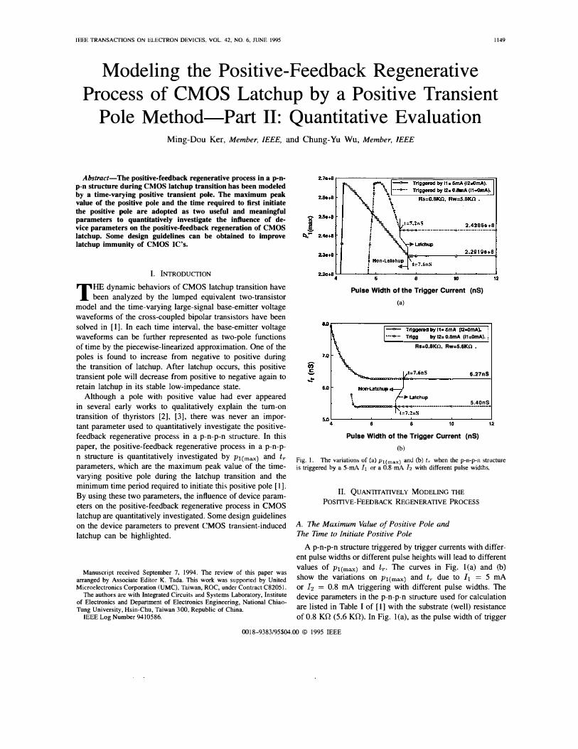
Fig. 1. The variations of Ca) Pl(max) and (b) tT when the p·n-p-n structure is triggered by a S-rnA It or a O.S-rnA h with different pulse widths.
II. QUA NTITATIVELY MODELING THE
POSmvE-FEEDBACK REGENERATIVE PROCESS
A. The Maximum Value of Positive Pole and The Time to Initiate Positive Pole
A p-n-p-n structure triggered by trigger currents with differ
ent pulse widths or different pulse heights will lead to different
values of Pl(max) and lr. The curves in Fig. I(a) and (b)
show the variations on Pl(max) and t,. due to h = 5 rnA
or 12 = 0.8 rnA triggering with different pulse widths. The
device parameters in the p-n-p-n structure used for calculation
are listed in Table I of [I] with the substrate (well) resistance
of 0.8 Kf2 (5.6 Kf2). In Fig. l(a), as the pulse width of trigger
0018-9383/95$04.00 © 1995 IEEE
1150
u;s. --
3.00+8r-----------::=;;;:;::;;""" ..... --�"'I IKF2; 4.8678-4
2.50+8
2.00+8
1.58+8
Rs�8000, Rw�5.6KO. 1.00+8
Irlggered by 11� SmA, Ian$.
_·-W-" b1ggered by 12= O.6mA. 10nS.
5·o.+;O�·7. -��l�O-; .• ,.....=:::;,O=.';:::::==l:O.::;:'==:,::;:O::;.'=:.......J,o.
IKF1 (A)
(a)
�.8r_-----------------__, IKFl � 6.9098-4
Trlggo.ed by II; SmA, IOn$. Irlggorad by 12= 0.6mA, IOnS.
'0" 1 0" 1 0"
IKF2 (A)
(b)
1 O' 10'
"r---r=7=�==========�==��===>--, IKF1 varying with. fixed IKF2=4.887H
10
10"
IKf2 varying wl1h. flxtclIKF1=6.90ge-4. IKFI varying wlUl • flxod IKF2=4.867.-1. IKF2 varying wllb • fixed IKF1=6.90ge-4.
Rs; 8000, R_ 5.6Kn.
Trlgger.d by 12=O.6mA, 10nS.
10"
IKF1 or IKF2 (A)
(c)
10' 10'
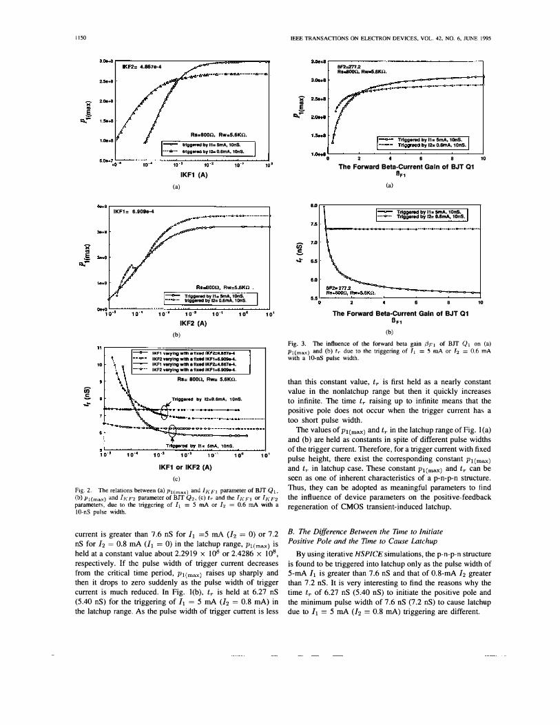
Fig. 2. The relations between (a) Pl(max) and IK Fl parameter of BJT Q" (b) Pl(max) and If{ F2 parameter of BIT Q2, (c) tr and the If{ Fl or IK F2 parameters, due to !he triggering of 1, = 5 rnA or 12 = 0.6 rnA with a lOonS pulse width.
current is greater than 7.6 nS for h =5 rnA (/2 = 0) or 7.2 nS for h = 0.8 rnA (h = 0) in the latchup range, Pl(max) is
held at a constant value about 2.2919 x J08 or 2.4286 x J08,
respectively. If the pulse width of trigger current decreases
from the critical time period, Pl(rnax) raises up sharply and then it drops to zero suddenly as the pulse width of trigger
current is much reduced. In Fig. I(b), tr is held at 6.27 nS
(5.40 nS) for the triggering of h = 5 rnA (/2 = 0.8 rnA) in
the latchup range. As the pulse width of trigger current is less
IEEE TRANSACTIONS ON ELECTRON DEVICES, VOL. 42, NO.6, JUNE 1995
'S' E
r::.,-;::
u;-S. ...t"
3�r----------------------------------, BF2:2T7.2 RI.aooo, RwQ.61ffi.
3.08+8 ____ --------..--0--<01
2..5e+8
T�gg.red by 11= 5mA, 1OnS. T�ggreed by 12= O.6mA, 10nS.
1.Oe.aL�-�.......'::=::::;===::::::;:==:::::;:=::.....-J
8.0
7.5
7.0
6.5
e.o
5.5 0
o 2. 4 6 8 ro The Forward Beta-Current Gain of BJT Q1
OF' (a)
1- Triggered by 11= SmA, ,ons. 1 n....... TrIggered by Ih G.8mA, IOnS ..
1--__ ........ -0 .. -0-0--••••• 0---.---0 ...•. --0---0 ...•. --.-.• ---0---
6 8
The Forward Beta-Current Gain of BJT Q1 BF1
(b)
10
Fig. 3. The influence of the forward beta gain PFI of BJT Q, on (a) Pl(max) and (b) tr due to Ihe triggering of '1 = 5 rnA or '2 = 0.6 rnA wi!h a lOonS pulse width.
than this constant value, tr is first held as a nearly constant value in the nonlatchup range but then it quickly increases
to infinite. The time tr raising up to infinite means that the
positive pole does not occur when the trigger current has a
too short pulse width.
The values of PI (max) and t,. in the latchup range of Fig. I(a)
and (b) are held as constants in spite of different pulse widths
of the trigger current. Therefore, for a trigger current with fixed
pulse height, there exist the corresponding constant Pl(max) and t,. in latchup case. These constant Pl(max) and tT can be
seen as one of inherent characteristics of a p-n-p-n structure.
Thus, they can be adopted as meaningful parameters to find
the influence of device parameters on the positive-feedback
regeneration of CMOS transient-induced latchup.
B. The Difference Between the Time to Initiate Positive Pole and the Time to Cause Latchup
By using iterative HSPICE simulations, the p-n-p-n structure
is found to be triggered into latchup only as the pulse width of 5-mA h is greater than 7.6 nS and that of 0.8-mA h greater
than 7.2 nS. It is very interesting to find the reasons why the
time tr of 6.27 nS (5.40 nS) to initiate the positive pole and
the minimum pulse width of 7.6 nS (7.2 nS) to cause latchup due to h = 5 rnA (/2 = 0.8 rnA) triggering are different.
KER AND WU: MODEUNG TIIE POSITIVE-FEEDBACK REGENERATIVE PROCESS OF CMOS LATCHUP-PART " 1151
3.O8+8,----------------------, BF1=I.104 •• 0······ Rs=8000, RW=5:�::�.4 •• 4
•• 4 •
• 4.-D-.�.-�--·D ...... -••
2.08+8
1- Trlgge"'" by 11= SmA, IDnS. 1 ------ Trine"'" by 12= 0 .6mA, IOnS. o.oe.o L�-��========��
o 100 200 300 400 !500
The Forward Beta-Current gain of BJT Q2 Bf2
(a)
grri:------��������� 1 - Triggeredbyl1=5mA,IOnS. 1 8
7
I�
i 1'---'- Trlgge"'" by 12 = o.8mA. IonS. � '\
" ..
.,."0'0'0"0 .... 0-...... 0
.....
.......... 0 ... 0 •• "'0 ........ "'0 •• -0 ........
0 ....... ...
BFI=1.104 Rs=BDOO, Rw=5.6KO.
6 �---� ____ -L ____ � ____ � __ �-J o 100 200 300 400
The Forward Beta-Current Gain of BJT Q2 BF2
(b)
500
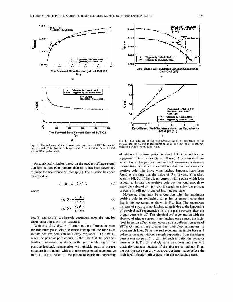
Fig. 4. The influence of the forward beta gain (3P2 of BIT Q2 on (a) Pl(max) and (b) tr due to the uiggering of It = 5 rnA or I2 = 0.6 rnA with a lO-nS pulse width.
An analytical criterion based on the product of large-signal
transient current gains greater than unity has been developed
to judge the occurrence of latchup [4]. The criterion has been
expressed as
(1)
where
(2)
(3)
(J1tr ( t) and (J2tr (t) are heavily dependent upon the junction
capacitances in a p-n-p-n structure.
With this "(J1tr . (J2tr � I" criterion, the difference between
the minimum pulse width to cause latchup and the time tr to
initiate positive pole can be clearly explained. The time tn when the positive pole occurs, is the time that the positive
feedback regeneration starts. Although the starting of the
positive-feedback regeneration will quickly push a p-n-p-n
structure into latchup with a double exponential regenerative
rate [I], it still needs a time period to cause the happening
.. .. .s
1:1,-
2.68+8
2Ae+8
2.21+11 Triggs"'" by l1=SmA, IOnS. Triggs"'" by 12= 0.6mA, lDnS.
2.08+8.1 10
Zero-Biased Well-Substrate Junction Capacitance Cjc1+Cjc2 (pF)
(al
1'.0,----------------:Jr-----,
9.0
ClehO.6pF, Cle2=1.3pF; R8=BODO, Rw=5.6KO. CIC1=Clc2
Triggered by l1=smA, IonS. Triggered by 12=O.6mA, Ions'
3.0 0 2 4 6 8 10
Zero-Biased Well-Substrate Junction Capacitance Cjc1+Cjc2 (pF)
(b)
Fig. 5. The influence of the well-substrate junction capacitance on (al Pl(m.x)and (b) tr, due to the uiggering of It = 5 rnA or h = 0.6 rnA triggering with a 10-nS pulse width.
of latchup. This time period is about 1.33 (1.8) nS for the
triggering of h = 5 rnA (12 = 0.8 rnA), A p-n-p-n structure which has a stronger positive-feedback regeneration needs a
shorter time period to cause latchup after the occurrence of positive pole. The time, when latchup happens, have been found as the time that the value of (J1tr (t) . (J2tT (t) reaches
to unity [4]. So, if the trigger current with a pulse width long enough to initiate the positive pole but not long enough to make the value of (Jltr (t) . (J2tr (t) reach to unity, the p-n-p-n structure is still not triggered into latchup state.
Moreover, there may be a question why the maximum positive pole in nonlatchup range has a greater value than
that in latchup range, as shown in Fig. I(a). The anomalous increase of Pl(max) in nonlatchup range is due to the happening
of physical self-regeneration in a p-n-p-n structure after the trigger current is off. This physical self-regeneration with the absence of trigger current in nonlatchup case causes the highlevel injection effect, which occurs as the collector currents of BJT's Q1 and Q2 are greater than their IKF parameters, to occur much later. Since the self-regeneration in the base and collector currents without enough supporting from the trigger current can not push (J1tr . (J2tr to reach to unity, the collector currents of BJT's Q1 and Q2 raise up slower and then will gradually decrease because of the absence of latchup. Thus, the positive pole can grow up toward a larger value before the
high-level injection effect occurs in the nonlatchup case.
1152
2.68+8 r-----;:==:;===.:=.:====:::::;---, 1-- Triggered by 11= SmA,10nS. 1 .
.....
.. Triggered bV 12= O.6mA, 10nS. 1
2.58+8 ........
.
.............
......
....................
...............
.........
............. . 2.4e+8
2.38
+8 r�-o-----------_-_____ ....J Rs=800C, Rw-..5.6Kn; Cje2=1.3pF, Clc2=D.6pF; Cjcl =2.0pF. 2.2e+8L------�--�--�--------'
a 1 2 3 Zero·Blased Base-Emitter Junction Capacitance of BJT Q1
Cje1 (PF)
(a)
9.0 r;::::::::::::=;::;::�::::::;::;;�:7:;;::;;:=::;_------1 1 1-- TrllIII_byll=5mA,10nS. 1
I I··· ... ·· Triggered by 12: O.6mA, 10nS.
8.0
oO'"� .. 7.0
Ro=8OOn, Rw=5.6Kn; CJe2=1.3pF, CJc2=D.6pF; CJcl=2.OpF. • •••
� .
..
.
..
.
..
.
...
...
.......
..
... ..
� ...
...........
.........
.....
.. -
... .
--......-----I ......... 6.00L------�----- ........ --------'
Zero-Biased Base-Emitter JunctIon CapacItance of BJT Q1 Cje1 (pF)
(b)
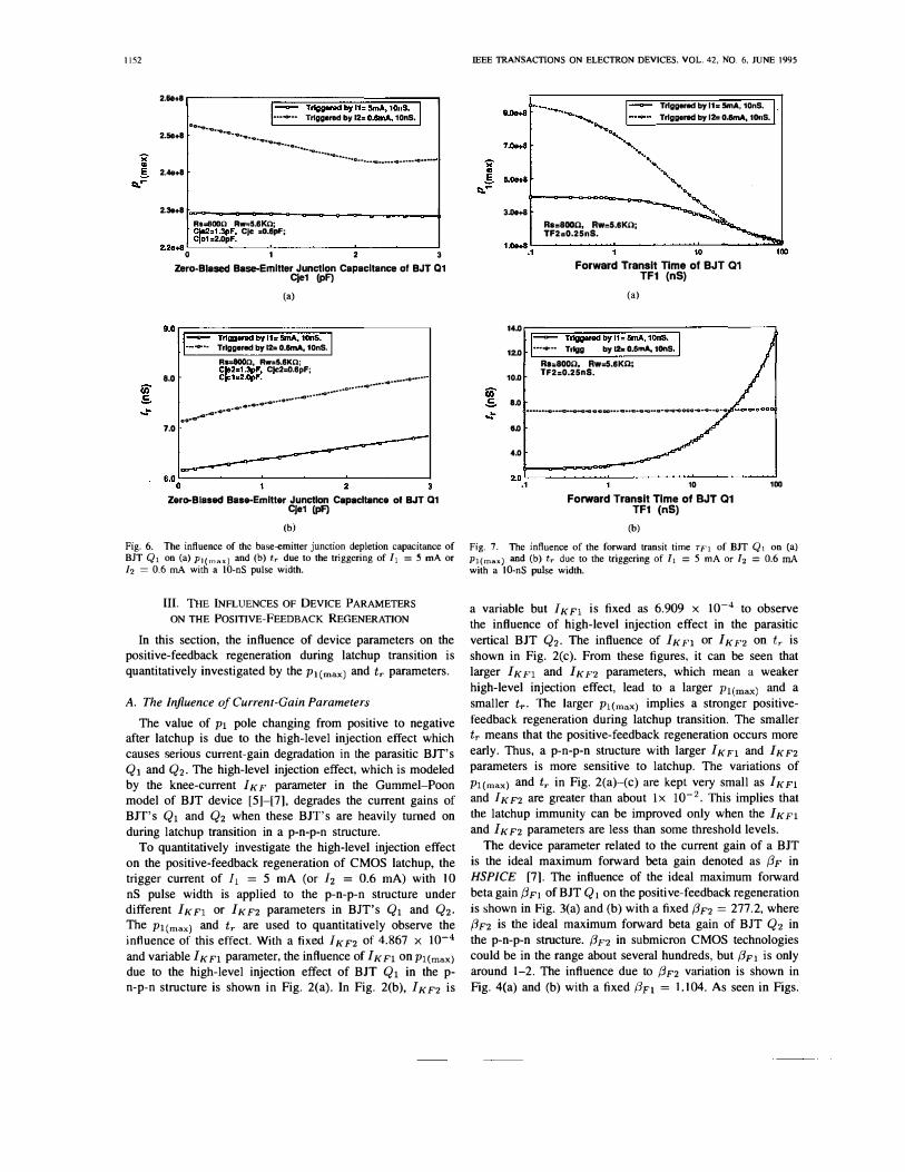
Fig. 6. The influence of the base-ilmitter junction depletion capacitance of BJT Ql on (a) p, (max) and (b) tr due to the triggering of 1, = 5 rnA or 12 = 0.6 rnA with a lO·nS pulse width.
III. THE INFLUENCES OF DEVICE PARAME TERS
ON THE POSITIVE-FEEDBACK REGENERATION
In this section. the influence of device parameters on the positive-feedback regeneration during latchup transition is quantitatively investigated by the Pl(rnax) and tr parameters.
A. The Influence of Current·Gain Parameters
The value of Pl pole changing from positive to negative after latchup is due to the high-level injection effect which causes serious current-gain degradation in the parasitic BJT's Ql and Q2. The high-level injection effect, which is modeled by the knee-current I K F parameter in the Gummel-Poon model of BJT device [5]-[7], degrades the current gains of BJT's Ql and Q2 when these BJT's are heavily turned on during latchup transition in a p-n-p-n structure.
To quantitatively investigate the high-level injection effect on the positive-feedback regeneration of CMOS latchup, the trigger current of h = 5 rnA (or 12 = 0.6 rnA) with 10 nS pulse width is applied to the p-n-p-n structure under different 1KFl or 1KF2 parameters in BJT's Ql and Q2. The Pl(max) and tr are used to quantitatively observe the influence of this effect. With a fixed 1KF2 of 4.867 x 10⁻⁴ and variable 1KFl parameter, the influence of 1KFl on Pl(rnax) due to the high-level injection effect of BJT Ql in the pn-p·n structure is shown in Fig. 2(a). In Fig. 2(b), 1K F2 is
IEEE TRANSACTIONS ON ELECTRON DEVICES. VOL. 42. NO.6. JUNE 1995
3Jle+8 Rs=8000, Rw=5.6KO; TF2=0.25nS.
Triggered by 11= SmA, 10nS. Triggered by 12: O.6mA, lOnS.
1Jle+8.Ll--------��1--��----�10�--���� Forward Transit Time of BJT Q1
TF1 (nS)
(a)
14.0 r;::::;::=;;::;:::=':;:::::;;::::;='=:;::;�;-----l 1-- Triggered by 11=5mA,10nS. 1 ........ Triggered by Ib MonA, lOnS .
. 12.0
10.0
8.0
6.0
4.0
Ra:80DO, Rw=5.6Kn; TF2=0.25nS.
·······O···'O··O_..,OOOO··· ... ··o .... "CI··a·'O"V�OOO-o·,o·-O-'O
�OL---------�u---------��--------�� .1 10 100
Forward Transit Time of BJT Q1 TF1 (nS)
(b)
Fig. 7. The influence of the forward transit time TFI of BIT Q, on (a) Pl(max) and (b) tr due to the triggering of 1, = 5 rnA or 12 = 0.6 rnA with a 10· nS pulse width.
a variable but 1KFl is fixed as 6.909 x 10⁻⁴ to observe the influence of high-level injection effect in the parasitic vertical BJT Q2. The influence of 1KFl or 1KF2 on tr is shown in Fig. 2(c). From these figures, it can be seen that larger 1KFl and 1KF2 parameters, which mean a weaker high-level injection effect, lead to a larger Pl(rnax) and a smaller tr. The larger Pl(max) implies a stronger positivefeedback regeneration during latchup transition. The smaller tr means that the positive-feedback regeneration occurs more early. Thus, a p-n-p-n structure with larger 1KFl and 1KF2
parameters is more sensitive to latchup. The variations of Pl(max) and tr in Fig. 2(a)-(c) are kept very small as 1KFl
and 1KF2 are greater than about Ix 10-2• This implies that the latchup immunity can be improved only when the 1KFl
and I K F2 parameters are less than some threshold levels. The device parameter related to the current gain of a BIT
is the ideal maximum forward beta gain denoted as {3 F in HSPICE [7]. The influence of the ideal maximum forward beta gain (3 F1 of BJT Q 1 on the positi ve-feedback regeneration is shown in Fig. 3(a) and (b) with a fixed {3F2 = 277.2, where fJF2 is the ideal maximum forward beta gain of BJT Q2 in the p-n-p-n structure. {3F2 in submicron CMOS technologies could be in the range about several hundreds, but {3Fl is only around 1-2. The influence due to (3F2 variation is shown in Fig. 4(a) and (b) with a fixed {3F1 = 1.104. As seen in Figs.
KER AND WU: MODELING THE POSITIVE-FEEDBACK REGENERATIVE PROCESS OF CMOS LATCH UP-PART II 1153
Ui S. .. �
1.08+8
Trlgganod by 11= 5mA, IOnS. Trlgganod by 12= 0. 8mA, IOnS. Rs=BODU, Rw=5.6KU; TF1=20nS.
0�.Ll------�----���
I-----L----------�
10
11.0
10.0
9.0
B.O
7.0
6.0 . 1
Forward Transit Time of BJT 02 TF2 (nS)
(a)
TrI_redbyll=5mA.10nS. I ! Trtggered by 12= O.8mA, IOnS. i
Rs=BODU, Rw=S.8KO; ,/ TF1=20nS. / /' "
,/ 4J�.d''''o
," •• � ..... _.CII .........
.o"",,"G
1 Forward Transit Time of BJT 02
TF2 (nS)
(b)
-
10
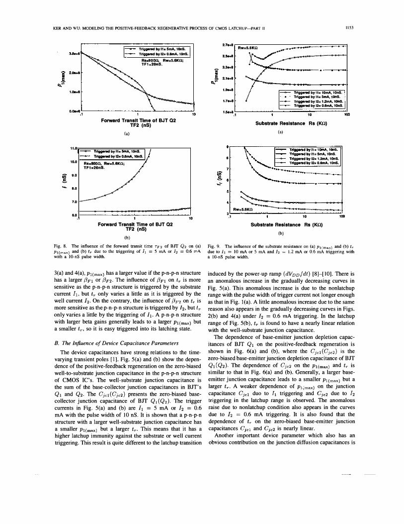
Fig. 8. The influence of the forward transit time TF2 of BIT Q2 on (a) Pl(max) and (b) tr due to the triggering of h = 5 rnA or [2 = 0.6 rnA with a lO-nS pulse width.
3(a) and 4(a), Pl(max) has a larger value if the p-n-p-n structure has a larger {3Fl or {3F2. The influence of {3F1 on tr is more sensitive as the p-n-p-n structure is triggered by the substrate current h, but t,. only varies a little as it is triggered by the well current 12. On the contrary, the influence of (3F2 on tT is more sensitive as the p-n-p-n structure is triggered by 12, but tr only varies a little by the triggering of h. A p-n-p-n structure with larger beta gains generally leads to a larger Pl(max) but a smaller t,., so it is easy triggered into its latching state.
B. The Injiuence of Device Capacitance Parameters
The device capacitances have strong relations to the timevarying transient poles [1]. Fig. Sea) and (b) show the dependence of the positive-feedback regeneration on the zero-biased well-to-substrate junction capacitance in the p-n-p-n structure of CMOS IC's. The well-substrate junction capacitance is the sum of the base-collector junction capacitances in BJT's Ql and Q2. The Cjel (Cjc2) presents the zero-biased basecollector junction capacitance of BJT QI(Q2). The trigger currents in Fig. Sea) and (b) are h = S rnA or 12 = 0.6 rnA with the pulse width of 10 nS. It is shown that a p-n-p-n structure with a larger well-substrate junction capacitance has a smaller PI (max) but a larger tT• This means that it has a higher latchup immunity against the substrate or well current triggering. This result is quite different to the latchup transition
'iC .. .s
r:., ....
2.7_
2.5e+8
2._
2.1_
1.geHI
1.7_
1.58+8 .1
Rw=5.6KO ....... ..................... __ .... ..... _ ............. -..... .
". .......... / -0000 .............. -••• 0 .. 0•0 •• 0•
J Qa ..... • .... • ..
...... .,g
.. ·o .. qoO
/ I
p' .' � ..
Triggered by 11= 10mA, IOnS. Trt� by 11= SmA. IOnS. Trl_red by 12= I.2mA, IOnS. Trtggered by 12= 0.8mA, IOnS.
10
Substrate Resistance Rs (KG)
(a)
9r---�------IC==�TrI� g� g.�m�bY�II�.� 10rnA��.I
���S.
�
8
4
3 .1
TrIggered by 11= 5mA, IOnS. TrIggered by 12= l.2mA. IOnS. Triggered by 12= 0.8mA, Ions.
........ " ..... _=----------�---...... o-o�
Rw:5.6KO "0"000 ••••• _-'0 .•.•.• 0-.-0.1:100 __ ..... _0 .
......... '0.'0.0._0_
10
Substrate Resistance Rs (KG)
(b)
100
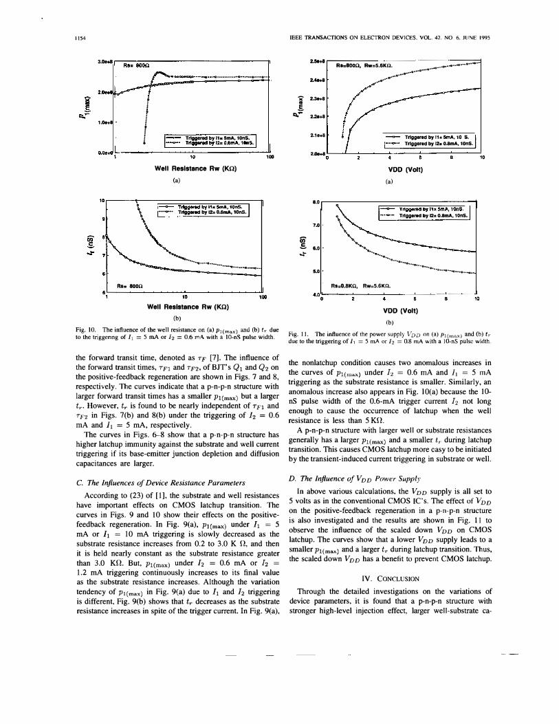
Fig. 9. The influence of the substrate resistance on (a) PI (max) and (b) tr due (0 It = 10 rnA or 5 rnA and h = 1.2 rnA or 0.6 rnA triggering with a lOonS pulse width.
induced by the power-up ramp (dVDD/dt) [8]-[10]. There is an anomalous increase in the gradually decreasing curves in Fig. Sea). This anomalous increase is due to the nonlatchup range with the pulse width of trigger current not longer enough as that in Fig. lea). A little anomalous increase due to the same reason also appears in the gradually decreasing curves in Figs. 2(b) and 4(a) under 12 = 0.6 rnA triggering. In the latchup range of Fig. S(b), t,. is found to have a nearly linear relation with the well-substrate junction capacitance.
The dependence of base-emitter junction depletion capacitances of BJT Ql on the positive-feedback regeneration is shown in Fig. 6(a) and (b), where the Cjel(Cje2) is the zero-biased base-emitter junction depletion capacitance of BJT Ql(Q2). The dependence of Cje2 on the PI (max) and tT is similar to that in Fig. 6(a) and (b). Generally, a larger baseemitter junction capacitance leads to a smaller PI(max) but a larger tr. A weaker dependence of Plimax) on the junction capacitance Cjel duo to h triggering and Cje2 due to lz triggering in the latchup range is observed. The anomalous raise due to nonlatchup condition also appears in the curves due to lz = 0.6 rnA triggering. It is also found that the dependence of tr on the zero-biased base-emitter junction capacitances Cjel and Cje2 is nearly linear.
Another important device parameter which also has an obvious contribution on the junction diffusion capacitances is
1 154
3.0l1+li r-;:;R;::"s=--;;:80;;;O:::n:---------------, �.OOOOOODClO-.---O--.. ""' ........ -............. O .... -O ••
I� 2.0e+8� t � i ; 1.0e+8 I 1 t .. _.. Triggered by 11z SmA, 10nS. 1
I" Triggered by 12= O.6mA, lOnS.
O·oe.ol!------�===========�J 10 100
Well Resistance Rw (Kn)
(a)
10 I-';-r.��;;::::::::;;:�:;::::::::;::;:::;-----l \ 1-- Triggeredbyll.5mA,10nS. I " ... _.. Triggered by 12= 0.1ImA, 10nS . .
" 0 ........... ."0 .... -0 ................. "0 .......... _ ••
Rs= 8000 5�1---------------�10�--�-------� 100 Well Resistance Rw (KQ)
(b)
Fig. 10 . . The influence of the well resistance on (a) Pl(max) and (b) tr due to the tnggenng of h = 5 rnA or I2 = 0.6 rnA with a lO-nS pulse width.
the forward transit time, denoted as TF [7]. The influence of the forward transit times, TFI and TF2, of BIT's Ql and Q2 on the positive-feedback regeneration are shown in Figs. 7 and 8,
respectively. The curves indicate that a p-n-p-n structure with
larger forward transit times has a smaller Pl(max) but a larger
t,.. However, tr is found to be nearly independent of TFl and TF2 in Figs. 7(b) and 8(b) under the triggering of 12 = 0.6 rnA and II = 5 rnA, respectively.
The curves in Figs. 6--8 show that a p-n-p-n structure has higher latchup immunity against the substrate and well current triggering if its base-emitter junction depletion and diffusion
capacitances are larger.
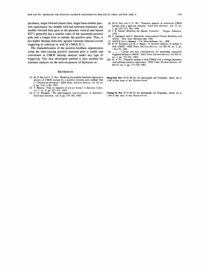
C. The Influences of Device Resistance Parameters
According to (23) of [1], the substrate and well resistances
have important effects on CMOS latchup transition. The
curves in Figs. 9 and 10 show their effects on the positivefeedback regeneration, In Fig. 9(a), PI (max) under h = 5 rnA or h = 10 rnA triggering is slowly decreased as the
substrate resistance increases from 0.2 to 3.0 K n, and then
it is held nearly constant as the substrate resistance greater
than 3.0 Kn. But, PI(max) under h = 0.6 rnA or 12 =
1.2 rnA triggering continuously increases to its final value as the substrate resistance increases. Although the variation
tendency of PI(max) in Fig. 9(a) due to h and h triggering
is different, Fig. 9(b) shows that tr decreases as the substrate resistance increases in spite of the trigger current. In Fig. 9(a),
IEEE TRANSACTIONS ON ELECTRON DEVICES. VOL. 42. NO. 6. JUNE 1995
" .. oS
r:.,. ..
'iii S. .:-
2.5e+8
2._
2.30+8
2.28+8
2. 10+8
2_ 0
R8=8000, RW�
.
�:::.
:: .....
.....
.......................
.....
...
.. ..
....
r l Triggered by 11= SmA, IOnS.
Triggered by 12. 0.8mA, 10n5.
4
VDD (Volt)
(a)
8
8.0 I'---��;;;;:;::::::;:::;::;:::;::;;::;! Trlgg __ by 11 = 5mA, IOnS.
7.0
6.0
5.0
"\ Trlgge_ by 12= 0.8mA, 10n5.
... \" ".
'O..�·o.
•
.
.. o···�·
···--···_· ..
·•·· ...
...... o ____
.
...
___ ..
Rs=0.8KO, Rw=5.6KO.
4.DO��--:------4:-�----':'-----8�---.--Jl0
VDD (Volt)
(b)
10
Fig.11. The influence of the power supply V'DD on (a) Pl(max) and (b) te due to the tnggenng of 1, = 5 rnA or I2 = 0.8 rnA with a lO·nS pulse width.
the nonlatchup condition causes two anomalous increases in the curves of PI(rno.x) under 12 = 0.6 rnA and II = 5 rnA triggering as the substrate resistance is smaller. Similarly, an
anomalous increase also appears in Fig. lOCal because the IOnS pulse width of the 0.6-rnA trigger current 12 not long
enough to cause the occurrence of latchup when the well
resistance is less than 5 Kn. A p-n-p-n structure with larger well or substrate resistances
generally has a larger Pl(max) and a smaller tf' during latchup transition. This causes CMOS latchup more easy to be initiated by the transient-induced current triggering in substrate or well.
D. The Influence of VDD Power Supply In above various calculations, the VDD supply is all set to
5 volts as in the conventional CMOS IC's. The effect of VDD on the positive-feedback regeneration in a p·n·p-n structure
is also investigated and the results are shown in Fig. II to
observe the influence of the scaled down VDD on CMOS
latchup. The curves show that a lower VDD supply leads to a
smaller Pl(max) and a larger tr during latchup transition. Thus, the scaled down VDD has a benefit to prevent CMOS latchup.
IV. CONCLUSION
Through the detailed investigations on the variations of device parameters, it is found that a p-n-p-n structure with
stronger high-level injection effect, larger well-substrate ca-
KER AND WU: MODELING THE POSITIVE-I'EEDBACK REGENERATIVE PROCESS OF CMOS LATCHUP-PART II 1155
pacitance, larger forward transit time, larger base-emitter junc
tion capacitance, but smaller well and substrate resistance, and smaller forward beta gain in the parasitic vertical and lateral BJT's generally has a smaller value of the maximum positive pole and a longer time to initiate the positive pole. Thus, it has higher latchup immunity against transient-induced current triggering in substrate or well of CMOS IC's.
The characterization of the positive-feedback regeneration using the time-varying positive transient pole is useful and convenient in CMOS latchup analysis under any type of triggering. This new developed method is also suitable for
transient analysis on the turn-on process of thyristors or
REFERENCES
[II M.-D. Ker and c.-Y. Wu, "Modeling the positive-feedback regenerative process of CMOS latchup by a po.itive tran.ient pole method: Part I-Theoretical derivation," IEEE Trans. Electron Devices, vol. 42, no. 6, pp. 1141-1148, 1995.
[21 T. Misawa, "Turn-on transient of p-n-p-n triode," J. Electron. Contr .. vol. 7, no. 6, pp. 523-533, 1959.
[3) G. D. Bergman, "The gate-triggered turn-on process in thyristors," Solid-State Electron., vol. 8, pp. 757-765, 1965.
(4) M.-D. Ker and c.-y. Wu, "Transient analysis of submicron CMOS latchup with a physical criterion," Solid-State Electron., vol. 37, no. 2, pp. 255 -273, Feb. 1994.
[5) l. E. Getreu, Modeling the Bipolar Transistor. Oregon: Tektronix, 1976.
(6) P. A ntognetti and G. Massobrio, Semiconductor Device Modeling with SPICE. New York: McGraw-Hili, 1988.
l7J HSPICE User's Manual. CA: Meta-Software, Inc., 1990. [8) R. R. Troutman and H. P. Zappe, "A transient analysis of latchup in
bulk CMOS," IEEE Trans. Electron Devices, vol. ED-30, no. 2, pp. 170-179, 1983.
[9] __ , "Layout and bias con.iderations for preventing transiently triggered 1atchup in CMOS," IEEE Trans. Electron Devices, vol. ED-3I, no. 3, pp. 315-321, 1984.
[10) K. Y. Fu, "Transient latchup in bulk CMOS with a voltage-dependent well-substrate junction capacitance," [EEE Trans. Electron Devices, vol. ED-32, no. 3, pp, 717-720, 1985.
Ming-Dou Ker (S'92-M'94), for photograph and biography, please see p. 1148 of this issue of this TRANSACTIONS.
Chung-Yu Wu (S'75-M'77) for photograph and biography, please see p. 1148 of this issue of this TRANSACTIONS.


![REGENERATIVE BRAKING SYSTEM IN ELECTRIC VEHICLES · REGENERATIVE BRAKING SYSTEM IN ELECTRIC VEHICLES ... REGENERATIVE BRAKING SYSTEM ... Regenerative action during braking[9]](https://img.pdfslide.us/doc/110x75/5adccef67f8b9a1a088c7cf0/regenerative-braking-system-in-electric-vehicles-braking-system-in-electric-vehicles.jpg)