Embed Size (px)
Citation preview

1
®®Southwest Test Workshop 1999
Rahima Mohammed06/07/1999
Modeling the Array Forceof C4 Probe Cards during
Wafer Sort
Rahima MohammedArun Ramamoorthy
Intel Corporation
2
®®Southwest Test Workshop 1999
Rahima Mohammed06/07/1999
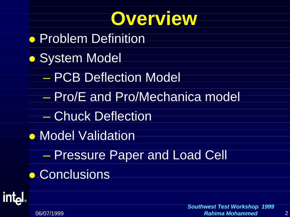
Overview! Problem Definition! System Model
– PCB Deflection Model– Pro/E and Pro/Mechanica model– Chuck Deflection
! Model Validation– Pressure Paper and Load Cell
! Conclusions
3
®®Southwest Test Workshop 1999
Rahima Mohammed06/07/1999
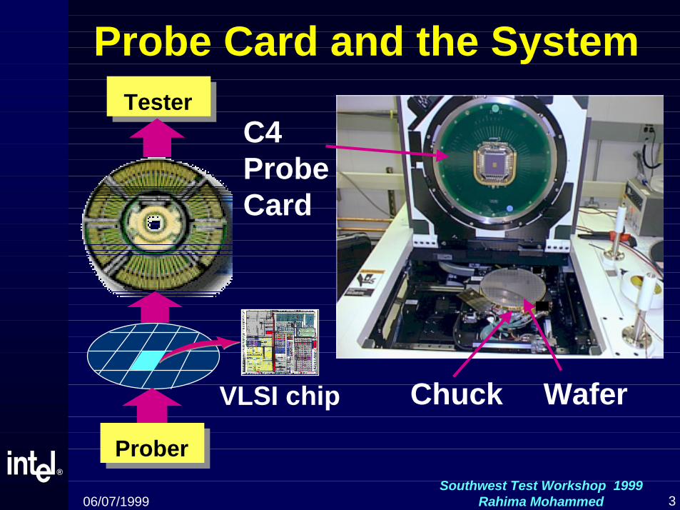
Probe Card and the System
VLSI chip
Tester
Prober
C4ProbeCard
Chuck Wafer

4
®®Southwest Test Workshop 1999
Rahima Mohammed06/07/1999
Contact Resistance and Model?! Contact Resistance (Cres) is the resistance
between the C4 bumps and the probes.! High power requirements of the products require
reducing Cres to achieve good electrical contact.! Without good Cres - False Failures and Yield
Reduction.! Control variable over Cres is overtravel (OT).! Overtravel (OT) required to achieve good Cres
during wafer sort varied with the product probecount.

5
®®Southwest Test Workshop 1999
Rahima Mohammed06/07/1999
Why do we need a Model?! Increase in probe count increases the array force
exerted by the probes on the chuck.! Normal contact force is due to the compression
of the probes, it is critical to model the actualcompression of the probes for an OTprogrammed (input) into the prober.
! Determine the array force on the chuck from theactual compression of the probes.

6
®®Southwest Test Workshop 1999
Rahima Mohammed06/07/1999
Schematic of the System
High power CPU sort requirements result in probecount increase and hence, increase in the arrayforce.
Wafer
C4 ProbesProbeCard
Chuck
PCB

7
®®Southwest Test Workshop 1999
Rahima Mohammed06/07/1999
System Modeling
F
F
F
F
F
kchuck
kspring
kPCB! PCB, Probes and Chuck treated as asystem of springs in series ( in equilibrium)
PCBspringschucksystem kkkk1111 ++=
PCBspringschucksystem kF
kF
kF
kF ++=
!Programmed OT = Chuck Deflection +Probe Compression + PCB Deflection

8
®®Southwest Test Workshop 1999
Rahima Mohammed06/07/1999
Objective
Variables! Overtravel(OT)! Probe Count! Die Location
Measured Quantity! PCB Deflection
Limitations! Prober to prober variation (ITTO prober only)! PCB to PCB variation! Variation in k -value
Develop a model to predict the array force on thechuck for an overtravel programmed into theprober

9
®®Southwest Test Workshop 1999
Rahima Mohammed06/07/1999
PCB Deflection Expt. Setup
S9K Testhead Emulator Dial Gage

10
®®Southwest Test Workshop 1999
Rahima Mohammed06/07/1999
Metrology Capability Study! MCA done on dial gage used to measure PCB
deflection (n=16 for accuracy evaluation, n=30for repeatability study on known thicknesssamples)–Precision/Tolerance (P/T) of 0.21
! The chuck z-movement was verified to checkfor any bias in the z-movement.– Chuck z-movement linear with OT with
a bias.

11
®®Southwest Test Workshop 1999
Rahima Mohammed06/07/1999
MCA Study (cont.)! To obtain a baselines for the Std. Dev., 30
measurements of the PCB Deflection weretaken on an Al wafer at 5 die locations eachand 4 OTs at each location.– PCB Deflection linear with OT with a slope
that varied based on the measured dielocation (due to variations in chuck deflectionat different die locations).

12
®®Southwest Test Workshop 1999
Rahima Mohammed06/07/1999
Experimental Design! Probe Count
–Started with C4 probe card and pluckedsets of 200 probes.
! Positional Dependence (30 random dielocations spread across the wafer).
! Overtravel (2 OT and 9 measurementsper OT).

13
®®Southwest Test Workshop 1999
Rahima Mohammed06/07/1999
Analysis! PCB deflection model by fitting the data
using stepwise statistical regressionanalysis.
! Higher order effects (>2) were included inthe model to start with and were droppedsubsequently based on their significancelevel.
! The model was validated by collectingdata with by removing another 100probes from the C4 probe card.

14
®®Southwest Test Workshop 1999
Rahima Mohammed06/07/1999
Model Validation
1015202530354045
-8 -7 -6 -5 -4 -3 -2 -1 0 1 2 3 4 5 6 7 8
Die X (for a fixed Die Y=0)
Def
lect
ion
(um
)
DataModel

15
®®Southwest Test Workshop 1999
Rahima Mohammed06/07/1999
Pro/E and Pro/Mechanica Modelof the PCB
Test Head EmulatorLoads
Constraints
Pro/E model
SideView
IsometricView
Pro/Mechanica Analysis of PCB Displacement Distribution

16
®®Southwest Test Workshop 1999
Rahima Mohammed06/07/1999
Empirical Model vs. FEM ModelS9k Force vs. Max. PCB Deflection
0102030405060708090
10 20 30 40 50Force (lbs)
PCB
Def
lect
ion
(um
)
Pro/E and Pro/Mechanica modelExperiment
Matched to within 5%
PCB Deflection varied linearly with OT.

17
®®Southwest Test Workshop 1999
Rahima Mohammed06/07/1999
Chuck Deflection Modeling
! Prober parameters used to build a model forthe chuck deflection–Chuck Deflection = f([X,Y], F,T); F = Force
and T= Temperature

18
®®Southwest Test Workshop 1999
Rahima Mohammed06/07/1999
Model Validation by C4 arrayForce Measurements
! S9K and J973 testheads do not haveaccess to make PCB deflectionmeasurements (can only be done atITTO Lab).
! Alternative techniques have beendeveloped to make array forcemeasurements on the sort floor.– Pressure paper and load cell
techniques
19
®®Southwest Test Workshop 1999
Rahima Mohammed06/07/1999
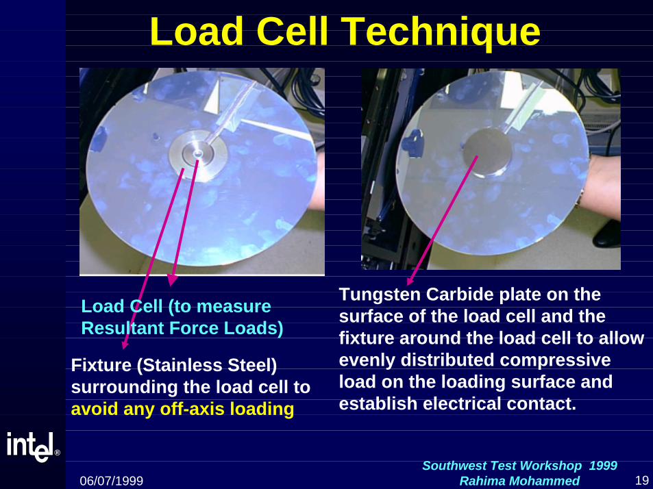
Load Cell Technique
Tungsten Carbide plate on the surface of the load cell and the fixture around the load cell to allow evenly distributed compressive load on the loading surface and establish electrical contact.
Fixture (Stainless Steel)surrounding the load cell toavoid any off-axis loading
Load Cell (to measureResultant Force Loads)

20
®®Southwest Test Workshop 1999
Rahima Mohammed06/07/1999
Pressure Paper TechniqueTwo - Sheet Prescale Film
343.03
71.12Initial Scan of the Die
Pseudo-Color Representationby Topaq Analyzer
(Pressure)

21
®®Southwest Test Workshop 1999
Rahima Mohammed06/07/1999
Combined Results
● Pressure paper technique matches the model closely and ismore useful in the production environment.● Load cell technique shows the right trend but with an offset andis useful in the Lab environment (Fast).
C4 Technology (Empirical Model, Pressure Paper and Load Cell)
0
5
10
15
20
25
30
35
60 80 100 120 140 160 180 200OT(um)
Forc
e (l
bs)
Super Low Pressure PaperModelLoad Cell

22
®®Southwest Test Workshop 1999
Rahima Mohammed06/07/1999
S9K vs J973 PCB Deflection
● Allowed to match actual probe compression betweenS9K and J973 to determine normal force per probe.● Obtain comparable Cres
0
10
20
30
40
50
60
70
0 5 10 15 20 25 30 35 40Force (lb)
Defle
ctio
n (
µ µµµm
)
J973 Deflection(um)S9K Deflection (um)
(Load Cell)C4 Technology
J973 systemstiffer than S9k

23
®®Southwest Test Workshop 1999
Rahima Mohammed06/07/1999
Conclusions! A novel model developed to predict the actual
compression of the probes in a C4 probe card asfunction of POT, die location on the wafer, and theprobe count.
! Pro/E and Pro/Mechanica analyses matched the PCBdeflection to within 5%.
! Pressure paper and Load Cell techniques matchedthe model and are good techniques to measure arrayforce when there is no access to make PCBdeflection measurements.
! Determine maximum probe count and chuck force.! Aid in optimization of sort OT’s.