Embed Size (px)
Citation preview
Active and Passive Elec. Comp.,
December 2003, Vol. 26, No. 4, pp. 197–204
MODELING OF THE I–V CHARACTERISTICS FORLDD-nMOSFETs IN RELATION WITH DEFECTS
INDUCED BY HOT-CARRIER INJECTION
R. MARRAKH* and A. BOUHDADA
Laboratoire de Physique des Materiaux et de Microelectronique, Universite Hassan II,Faculte des Sciences Aın Chok, Km8, Route d’El Jadida, BP 5366 Maarif,
Casablanca, Morocco
(Received 30 May 2002; In final form 3 July 2002)
The hot-carrier injection is observed increasingly to degrade the I–V characteristics with the scaling of MOStransistors. For the lightly doped drain MOS transistor the injection of the hot-carriers, caused by the highelectric field in the MOS structure, is localized in the LDD region. The modeling of the drain current in relationto defects due to the hot-carrier injection allows us to investigate the I–V characteristics and the transconductanceof devices. Consequently, we can know the amount of the device degradation caused by these defects in order tofind technological solutions to optimize reliability.
Keywords: I–V characteristics; MOS; LDD; Modeling; Defects
1 INTRODUCTION
One of the major problems that pose a serious constraint when reducing the channel length
of the MOS transistor is the hot-carrier caused by the high electric field in the device
structure. In order to reduce the hot-carrier effect, the LDD structure is used [1–3]. In
this structure, the electric field maximum is reduced and is spread out in the n-region.
However, hot-carriers are generated by impact ionization in the n-region under the sidewall
spacer [4–5]. This leads to the reduction of the free carrier mobility and to the increase of
the parasitic LDD resistance [6–8]. Understanding the physics of hot-carrier effects in sili-
con MOSFETs plays an important role in determining device degradation mechanisms and
thus the improvement of MOSFET design. So to study the effect of these defects on the
device reliability, it is very important to carry out a modeling of the I–V characteristics
in relation to defects localized in the LDD region. Simulations of their evolutions allow
us to know the amount of device degradation caused by these defects to find technological
solutions in order to minimize the aging phenomenon of the transistor.
* Corresponding author.
ISSN 0882-7516 print; ISSN 1563-5031 online # 2003 Taylor & Francis LtdDOI: 10.1080=08827510310001624363
2 MODELING OF THE DRAIN CURRENT
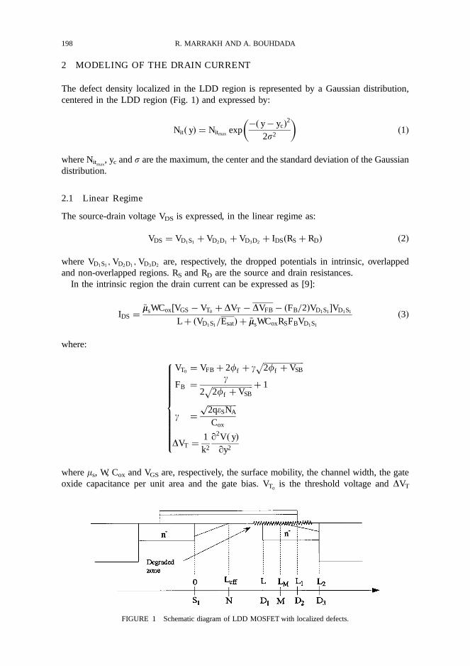
The defect density localized in the LDD region is represented by a Gaussian distribution,
centered in the LDD region (Fig. 1) and expressed by:
Nitð yÞ ¼ Nitmaxexp
�ð y � ycÞ2
2s2
� �ð1Þ
where Nitmax, yc and s are the maximum, the center and the standard deviation of the Gaussian
distribution.
2.1 Linear Regime
The source-drain voltage VDS is expressed, in the linear regime as:
VDS ¼ VD1S1þ VD2D1
þ VD3D2þ IDSðRS þ RDÞ ð2Þ
where VD1S1;VD2D1
;VD3D2are, respectively, the dropped potentials in intrinsic, overlapped
and non-overlapped regions. RS and RD are the source and drain resistances.
In the intrinsic region the drain current can be expressed as [9]:
IDS ¼�mmsWCox½VGS � VT0
þ DVT � DVFB � ðFB=2ÞVD1S1�VD1S1
L þ ðVD1S1=EsatÞ þ �mmsWCoxRSFBVD1S1
ð3Þ
where:
VT0¼ VFB þ 2ff þ g
ffiffiffiffiffiffiffiffiffiffiffiffiffiffiffiffiffiffiffiffiffi2ff þ VSB
pFB ¼
g2
ffiffiffiffiffiffiffiffiffiffiffiffiffiffiffiffiffiffiffiffiffi2ff þ VSB
p þ 1
g ¼
ffiffiffiffiffiffiffiffiffiffiffiffiffiffiffi2qeSNA
p
Cox
DVT ¼1
k2
q2V ð yÞ
qy2
8>>>>>>>>>><>>>>>>>>>>:
where ms, W, Cox and VGS are, respectively, the surface mobility, the channel width, the gate
oxide capacitance per unit area and the gate bias. VT0is the threshold voltage and DVT
FIGURE 1 Schematic diagram of LDD MOSFET with localized defects.
198 R. MARRAKH AND A. BOUHDADA
represents the threshold voltage reduction caused by the lateral electric field, which is very
weak in the linear regime that we can consider it as constant.
DVFB ¼qNitð yÞ
Cox
ms ¼m0
½1 þ yðVGS � VT0Þ�½1 þ bNitð yÞ�
Esat ¼2Wsat
m0
½1 þ yðVGS � VT0Þ�½1 þ bNitð yÞ�:
8>>>>>>>><>>>>>>>>:
ð4Þ
y and b are the fitting parameters. The spatial average of the defect density Nitð yÞ is
expressed as:
Nitð yÞ ¼
ffiffiffip2
rNitmax
sL
erfL � ycffiffiffi
2p
s
� �þ erf
ycffiffiffi2
ps
� �� �: ð5Þ
From Eq. (3) we derive VD1S1:
VD1S1¼
�V2 �ffiffiffiffiffiffiffiffiffiffiffiffiffiffiffiffiffiffiffiffiffiffiffiffiV 2
2 � 4V1V3
p2V1
ð6Þ
where:
V1 ¼�mmFBWCox
2
V2 ¼IDS
Esat
� �mmWCox½VGS � VT0þ DVT � DVFB � FBRsIDS �
V3 ¼ IDSL:
8>>>><>>>>:
The drain current at the overlapped-LDD region is expressed by:
IDS ¼W �mmsCox½ðVGS � VTn
þ DVT � DVFBÞ � FBnððVD2D1
=2Þ þ VD1S1Þ�VD2D1
ðL1 � LÞ½1 þ ðW �mmsCoxFBnRSVD2D1
Þ=ðL1 � LÞ þ VD2D1=EsatðL1 � LÞ�
: ð7Þ
From this equation we can obtain VD2D1as:
VD2D1¼
U2 �ffiffiffiffiffiffiffiffiffiffiffiffiffiffiffiffiffiffiffiffiffiffiffiffiffiU2 � 4U1U3
p
2U1
ð8Þ
U1 ¼�mmsFBn
WCox
2
U2 ¼ IDS W �mmsCoxRsFBnþ
1
Esat
� �� �mmsWCox½VGS � VTn
þ DVT � DVFB � FBnVD1S1
�
U3 ¼ IDSðL1 � LÞ:
8>>>>><>>>>>:
Using a similar method effectuated in the overlapped region, we derive the following
expression for the drain:
IDS ¼W �mms
�CCox½ðVGS � �VVTnþ DVT � DVFBÞ � �FFBn
ððVD3D2=2Þ þ VD2S1
Þ�VD3D2
ðL2 � L1Þ½1 þ ðW �mms�CCox
�FFBnRSVD3D2
Þ=ðL2 � L1Þ þ VD3D2=EsatðL2 � L1Þ�
: ð9Þ
LDD-n MOSFETs 199
Using expression (9) we obtain VD3D2as:
VD3D2¼
U 02 �
ffiffiffiffiffiffiffiffiffiffiffiffiffiffiffiffiffiffiffiffiffiffiffiffiffiU 0
2 � 4U 01U 0
3
p2U 0
1
ð10Þ
U 01 ¼
�mmsFBnW Cox
2
U 02 ¼ IDS W �mmsCoxRsFBn
þ1
Esat
� �� �mmsWCox½VGS � VTn
þ DVTn� DVFB � FBn
VD2S1�
U 03 ¼ IDSðL2 � L1Þ:
8>>>>><>>>>>:
The drain current in the linear regime is obtained by substituting VD1S1;VD2D1
and VD3D2
in Eq. (2).
2.2 Saturation Regime
When VDS becomes greater than the saturation voltage, the depleted zones in the intrinsic and
LDD region increase (Fig. 1). In this case VDS is written as:
VDS ¼ VMS1þ VD2M þ VD3D2
þ IDSðRS þ RDÞ: ð11Þ
VD3D2is given by the expression (10) and VD2M is obtained by replacing L by LM in Eq. (8).
Calculating VMS1gives the drain current in the saturation regime.
In the saturation region N< y<D1, the value of the lateral electric field becomes more
important and DVT cannot be regarded as a constant. From Eq. (3) we obtain the following
differential:
q2VCS1
qy2� p2VCS1
¼ p2 IDS
1 þ f RS
f�
VGS � VT0þ DVFB
FB
� �ð12Þ
where:
p2 ¼ FBk2
f ¼ WCoxWsatFB:
�
The boundary conditions at the pinch-off point ( point N) are: VCS1( y¼ Leff)¼Vdsat and
dVCS1
dy
��y¼Leff
¼ Esat. Using these boundary conditions the resolution of Eq. (12) gives the
potential along the channel in the saturation mode:
VCS1ð yÞ ¼ Vdsat þ
Esat
psinhð pð y � Leff ÞÞ
þ IDS
1 þ f RS
f�
VGS � VT0
FB
þ Vdsat
� �½coshð pð y � Leff ÞÞ � 1�
� p
ðy
Leff
DVFBð y0Þ
FB
sinhð pð y0 � yÞÞ dy0: ð13Þ
The saturation regime also leads to the creation of a depleted zone in the LDD region.
In the same way that in the case of the intrinsic region, the overlapped zone can be divided
200 R. MARRAKH AND A. BOUHDADA
into two regions. In the first region (M< y<D2) the variation of DVTnis weak whereas in the
second region (D1< y<M) and cannot be regarded as a constant.
In the saturation region the canal potential is governed by the following differential equation:
qVCS1
qy2� p2
nVCS1¼ p2
n IDS
1 þ fnRS
fn�
VGS � VTnþ DVFB
FBn
� �ð14Þ
p2n ¼
FBnCox
esxdn
fn ¼ WCoxWsatFBn:
8><>:
The boundary conditions at substrate-LDD junction are given by: VCS1( y¼ L)¼VL and
dVCS1
dy
��y¼L
¼ EL. VL and EL are determined using expression (13). Using the boundary
conditions, the resolution of Eq. (14) gives the channel potential in the saturation region:
VCS1ð yÞ ¼ VL þ
EL
pn
sinhð pnð y � LÞÞ
þ IDS
1 þ fnRS
fn�
VGS � VT0
FBn
þ VL
� �½coshð pnðy � LÞÞ � 1�
� pn
ðy
L
DVFBð y0Þ
FBn
sinhð pnð y0 � yÞÞ dy0 ð15Þ
at the point M we have: VCS1( y¼ LM)¼VMS1
and E( y¼ LM)¼Esat. From these boundary
conditions, one can obtain LM and VMS1. Thus, the drain current in the saturation regime
is obtained by substituting VMS1, VD2M and VD3D2
in Eq. (11).
3 SIMULATION RESULTS
The parameters of the transistor used in the simulation are given in Table I.
3.1 Defects Influence on the IDS –VDS Characteristic
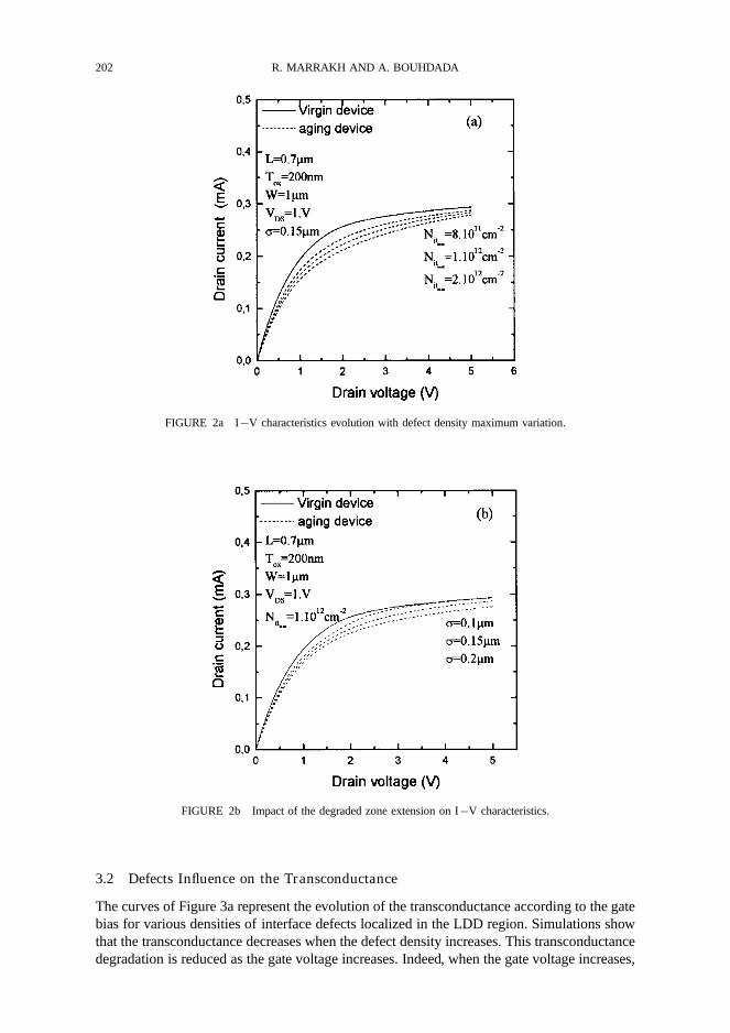
The curves of Figures 2a and 2b show the influence of the defects on characteristic IDS –VDS.
The presence of the defect density localized in the LDD region involves a reduction of the
current drain. This reduction is accentuated with the increase of the maximum of the defect
density (Figure 2a). The extension of the degraded zone also leads to the degradation of the
current drain (Figure 2b). In the saturation mode part, the interface states are in the velocity
saturation region and can be depleted, therefore the effect of these interface states becomes
insignificant.
TABLE I Transistor Parameters Used in Simulations.
Parameters Values
L=W 0.7mm=1mmL17 L=L27L 0.15mm=0.25mmTox =NA 20 nm=2.3� 1016 cm�3
y=b 0.18mm=2.5� 10�12
m0=Wsat 600 cm2V�1s�1=7� 106 cm s�1
LDD-n MOSFETs 201
3.2 Defects Influence on the Transconductance
The curves of Figure 3a represent the evolution of the transconductance according to the gate
bias for various densities of interface defects localized in the LDD region. Simulations show
that the transconductance decreases when the defect density increases. This transconductance
degradation is reduced as the gate voltage increases. Indeed, when the gate voltage increases,
FIGURE 2a I�V characteristics evolution with defect density maximum variation.
FIGURE 2b Impact of the degraded zone extension on I�V characteristics.
202 R. MARRAKH AND A. BOUHDADA
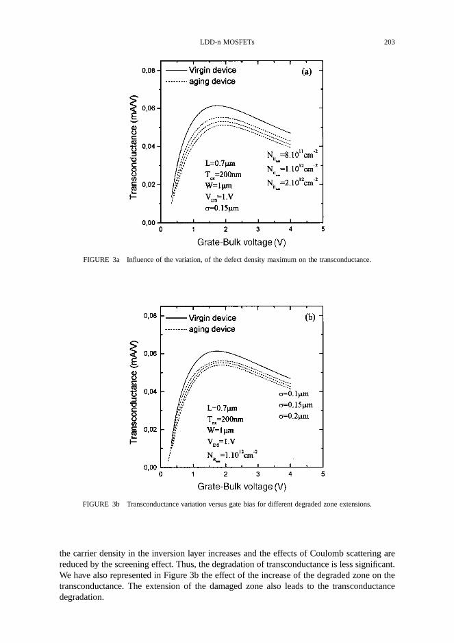
the carrier density in the inversion layer increases and the effects of Coulomb scattering are
reduced by the screening effect. Thus, the degradation of transconductance is less significant.
We have also represented in Figure 3b the effect of the increase of the degraded zone on the
transconductance. The extension of the damaged zone also leads to the transconductance
degradation.
FIGURE 3a Influence of the variation, of the defect density maximum on the transconductance.
FIGURE 3b Transconductance variation versus gate bias for different degraded zone extensions.
LDD-n MOSFETs 203
4 CONCLUSION
The modeling of the drain current for a lightly doped drain MOSFET in relation to defects
localized in the LDD region is very important. It allows us to understand the aging phenome-
non and the amount degradation of the performances of the devices. The simulation results
show that the stress leads to the degradation of the I–V characteristic and the reduction of the
transconductance. The model can be applied to the simulation of device behavior after stress
in order to improve the long-term circuit reliability.
References
[1] Takeda, E., Yang, C. Y. and Hamada, A. M. (1995). Hot-carrier effects in MOS devices. ed. Academic Press, INC.[2] Ang, D. S. and Ling, C. H. (1998). A unified model for the self-limiting hot-carrier degradation in LDD
n-MOSFETs. IEEE Trans. Electron. Dev., 45(1), 149–159.[3] Kinugawa, M., Kakumu, M., Yokogawa, S. and Hashimoto, K. (1985). Submicron MLDD n-MOSFETs for 5 V
operation. Tech. Dig. VLSI Tech. Symp., 116–117.[4] Huang, T. Y., Yao, W. W., Martin, R. A., Alan, G., Koyanagi, M. and Chen, J. Y. (1987). New LDD Transistor with
Inverse-T gate structure. IEEE Electron devices lett., 8, 151–153.[5] Huang, T. Y., Yao, W. W., Martin, R. A., Alan, G., Koyanagi, M. and Chen, J. Y. (1986). A novel submicron LDD
Transistor with Inverse-T gate structure. Tech. Dig -Int. IEEE Electron devices Meet., 742.[6] Yih, C. M., Wang, C. L., Chung, S. S., Wu, C. C., Tan, W., Wu, H. J., Pi, S. and Huang G, D. (1998). New insight
into the degradation mechanism of Nitride spacer with different post-oxide in submicron LDD n-MOSFETs.Jpn. J. Appl. Phys., 37, 1035–1040.
[7] Cheng, S. M., Yih, C. M., Yeh, J. C., Kuo, S. N. and Chung, S. S. (1997). A unified approach to profiling the lateraldistributions of both oxide charge and interface states in n-MOSFETs under various bias stress conditions. IEEETrans. Electron. Dev., 44(11), 1908–1913.
[8] Yang, J. J., Chung, S. S. S., Chou, P. C., Chen, C. H. and Lin, M. S. (1995). A new approach to modeling thesubstrate current of pre-stressed and post-stressed MOSFETs. IEEE Trans. Electron. Dev., 42(6), 1113–1119.
[9] Marrakh, R. and Bouhdada, A. (2001). Impact of the stress on the sub-micron n-metal oxide semiconductor fieldeffect transistor characteristics. Active and Passive Elec. Comp., 1–13.
204 R. MARRAKH AND A. BOUHDADA

International Journal of
AerospaceEngineeringHindawi Publishing Corporationhttp://www.hindawi.com Volume 2010
RoboticsJournal of
Hindawi Publishing Corporationhttp://www.hindawi.com Volume 2014
Hindawi Publishing Corporationhttp://www.hindawi.com Volume 2014
Active and Passive Electronic Components
Control Scienceand Engineering
Journal of
Hindawi Publishing Corporationhttp://www.hindawi.com Volume 2014
International Journal of
RotatingMachinery
Hindawi Publishing Corporationhttp://www.hindawi.com Volume 2014
Hindawi Publishing Corporation http://www.hindawi.com
Journal ofEngineeringVolume 2014
Submit your manuscripts athttp://www.hindawi.com
VLSI Design
Hindawi Publishing Corporationhttp://www.hindawi.com Volume 2014
Hindawi Publishing Corporationhttp://www.hindawi.com Volume 2014
Shock and Vibration
Hindawi Publishing Corporationhttp://www.hindawi.com Volume 2014
Civil EngineeringAdvances in
Acoustics and VibrationAdvances in
Hindawi Publishing Corporationhttp://www.hindawi.com Volume 2014
Hindawi Publishing Corporationhttp://www.hindawi.com Volume 2014
Electrical and Computer Engineering
Journal of
Advances inOptoElectronics
Hindawi Publishing Corporation http://www.hindawi.com
Volume 2014
The Scientific World JournalHindawi Publishing Corporation http://www.hindawi.com Volume 2014
SensorsJournal of
Hindawi Publishing Corporationhttp://www.hindawi.com Volume 2014
Modelling & Simulation in EngineeringHindawi Publishing Corporation http://www.hindawi.com Volume 2014
Hindawi Publishing Corporationhttp://www.hindawi.com Volume 2014
Chemical EngineeringInternational Journal of Antennas and
Propagation
International Journal of
Hindawi Publishing Corporationhttp://www.hindawi.com Volume 2014
Hindawi Publishing Corporationhttp://www.hindawi.com Volume 2014
Navigation and Observation
International Journal of
Hindawi Publishing Corporationhttp://www.hindawi.com Volume 2014
DistributedSensor Networks
International Journal of