Embed Size (px)
Citation preview
IEEE TRANSACTIONS ON MAGNETICS, VOL. 50, NO. 8, AUGUST 2014 4400307
Modeling of In-Plane Magnetic Tunnel Junctionfor Mixed Mode Simulations
Shivam Verma, Shalu Kaundal, and Brajesh Kumar Kaushik
Department of Electronics and Communication Engineering, Indian Institute of Technology Roorkee, Roorkee 247667, India
The incredible potentials of spin transfer torque (STT) magnetic random access memories (MRAMs) give them an edge overother memory technologies. Most of the projections show them as universal memory in the future; however, their evolution isstill in a rudimentary stage. Attaining a high density in STT MRAMs is imperative to keep pace with the scaling scenario infield effect transistors (FETs) and hence competitive with future processors. A vertical or a two terminal select device can be apossible solution to achieve the high-density problem. A suitable platform is required for simulating a hybrid magnetic tunneljunction (MTJ)/FET circuit before an actual fabrication is done. However, most simulation tools do not have the capability to modelhybrid MTJ/FET devices. Also, the SPICE compatible models for such devices and other novel structures like vertical FET are notavailable. This paper addresses the above-mentioned concerns and proposes a model for MTJ (coded in C++) and a simulationplatform for hybrid MTJ/FET device-circuit co-design with physics-based models. The proposed model is validated using mixed modesimulations.
Index Terms— Compact model interface (CMI), field effect transistors (FETs), mixed mode device/circuit simulation, spin transfertorque (STT).
I. INTRODUCTION
SPINTRONICS is considered as one of the most promisingtechnologies for the post CMOS era [1] which provides
an alternate state variable, that is, an electron’s spin orienta-tion. The evolution of spintronics goes back to the simplestspintronic device which exhibited the giant magnetoresistiveeffect (GMR) [2]–[4] known as spin valve. The discovery ofGMR effect led to the invention of a new class of mem-ory technology known as magnetic memories which storeddata as resistance state of a spin valve. GMR was a weakphenomenon which prompted to analogous device, that is,magnetic tunnel junction (MTJ) with a stronger resistancechange effect termed as tunnel magnetoresistive (TMR) effect.TMR is the normalized difference in resistance between par-allel (RAP) and antiparallel (RP ) magnetization configurationsexpressed as
TMR = RAP − RP
RP. (1)
MTJs have a tunnel barrier (insulator) separating two fer-romagnetic (FM) layers with different magnetic coercivity.Free layer has a low magnetic coercivity whose magnetizationorientation can be easily changed according to the fixed layerwith high magnetic coercivity. The resistance (RP ) is low inparallel and high (RAP) in antiparallel state. MTJs could beintegrated with CMOS technology because of good fabricationcompatibility and comparable impedance [5]. This led tothe evolution of magnetoresistive random access memories(MRAMs). The memory cells of MRAMs had one MTJ andone nMOS select device abbreviated as a 1T-1MTJ cell. Thefield of magnetic memory was revolutionized by the advent
Manuscript received September 12, 2013; revised January 17, 2014;accepted February 28, 2014. Date of publication March 11, 2014; date ofcurrent version August 15, 2014. Corresponding author: S. Verma (e-mail:[email protected]).
Color versions of one or more of the figures in this paper are availableonline at http://ieeexplore.ieee.org.
Digital Object Identifier 10.1109/TMAG.2014.2310181
of spin transfer torque (STT) effect and MgO tunnel barriers(large TMR). STT MRAMs emerged as a promising candidatefor universal memory technology with potentially superiorperformance in terms of speed, nonvolatility, low power andhigh density.
Design and simulation of STT MRAMs and hybridMTJ/FET circuits has been so far carried out on SPICE.The MTJs are represented by SPICE subcircuits or Verilog-A behavioral models. To date, the select devices of STTMRAM have been realized using planar FET technology only.The minimum attainable single cell size with planar FETs is6–8 F2, F being the feature size. To attain a higher 2-Ddensity, vertical select device or two terminal select devicesshould be used [1], [6]. Using vertical FET as select device,the cell area can be reduced up to 4 F2 [1]. The select devicesare gaining importance in emerging novel memory designs,and therefore a detailed analysis of their impact needs to bestudied. Vertically integrated nonlinear diodes and/or hetero-structures with large ON/OFF current ratio can also be used as aselect device to reach the optimistic figure of 4 F2 cell size [1].Parameterized SPICE models are not available for the novelstructured devices like vertical FET, therefore a system levelimpact on MRAMs cannot be analyzed on SPICE. Therefore,it is advisable to use mixed mode device-circuit simulation [7]to understand the effect of device design on MRAMs andnonvolatile logic circuits.
Various models have been proposed for MTJs as subcircuits[8]–[10] and Verilog-A behavioral–mathematical [11]–[14]models that are compatible with SPICE, but they cannot beemployed for device-circuit co-design. This paper proposesan advanced model of MTJ that is compatible with SentaurusTCAD (by Synopsys) for precise analysis of MTJ/FET circuitsand STT MRAMs. Encouragingly, the compatibility of theproposed model with a device simulator makes it suitableto study the effect of select device variations on the hybridMTJ/FET device-circuit co-design. The proposed model usesMTJ as a behavioral-mathematical model coded in C++,
0018-9464 © 2014 IEEE. Personal use is permitted, but republication/redistribution requires IEEE permission.See http://www.ieee.org/publications_standards/publications/rights/index.html for more information.
4400307 IEEE TRANSACTIONS ON MAGNETICS, VOL. 50, NO. 8, AUGUST 2014
whereas the select device is represented by material andphysical models in a device simulator. The proposed MTJmodel unlike other previous models includes submodels forboth precessional switching and temperature assisted switch-ing. In addition, it includes temperature dependencies of TMRand saturation magnetization.
This paper is arranged into seven sections including thecurrent introductory section. Section II illustrates the use of thecompact model interface (CMI) provided by Sentaurus TCADand the way in which it can be used to implement an MTJ. TheSection III precisely describes the device physics (macrospinmodel) of in-plane CoFeB/MgO/CoFeB MTJ and the analyt-ical equations used in the model to replicate the behavior.Section IV discusses the applicability of the macrospin model.Sections V and VI describe the model algorithm and simula-tion analysis for model validation, respectively. Finally, thepaper is concluded in Section VII.
II. USER DEFINED COMPACT MTJ MODEL
Sentaurus TCAD provides an interface for mixed modedevice-circuit analysis by instantiating compact models withtheir parameters known as compact model interface (CMI).Compact models can be either SPICE models or user-definedC++ models [15]. Considering these facts, this sectiondescribes about CMI and the way it can be used to implementan MTJ.
A. Compact Model Interface
Sentaurus solves a differential algebraic equation for anyuser-defined C++ compact model expressed as
d
dtq(t, Z(t)) + f (t, Z(t)) = 0. (2)
The time-dependent vector Z(t) consists of all unknownsfrom a user-defined compact model. The vector Z(t)consists of all electrode voltages (u1, u2, . . . , un), ther-mode temperatures (τ1, τ2, . . . , τn ) and internal variables(x1, x2, . . . , xn). The vector q(t, Z(t)) is the transient righthand side (RHS) and vector f (t, Z(t)) is called the dc right-hand side (RHS). The internal variables are generally the cur-rents (i1, i2, . . . , in) from electrodes into the compact model.The vectors q(t, Z(t)) and f (t, Z(t)) are computed based onthe functionality that user needs to implement through thecompact model. Sentaurus uses Newton’s method to solve(2) [16].
B. Implementation
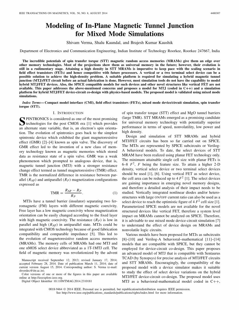
The simulation flow can be understood by a simplifiedblock diagram shown in Fig. 1. The inputs to the compactmodel are electrode voltages, currents (internal variables)and parameters. The model (shared object file) is linked toSentaurus Device (Simulation Engine) at run time throughdc and transient Jacobian and RHS matrices [15].
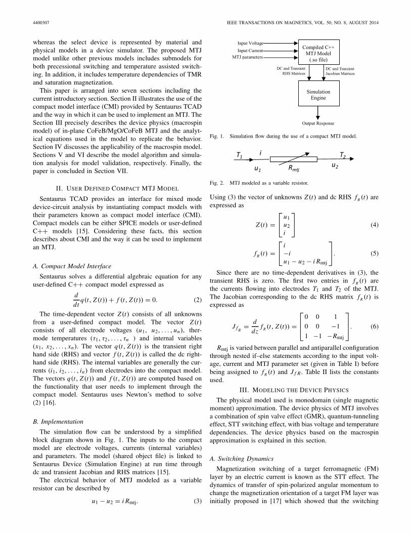
The electrical behavior of MTJ modeled as a variableresistor can be described by
u1 − u2 = i Rmtj. (3)
Fig. 1. Simulation flow during the use of a compact MTJ model.
Fig. 2. MTJ modeled as a variable resistor.
Using (3) the vector of unknowns Z(t) and dc RHS fR (t) areexpressed as
Z(t) =⎡⎣
u1u2i
⎤⎦ (4)
fR (t) =⎡⎣
i−iu1 − u2 − i Rmtj
⎤⎦. (5)
Since there are no time-dependent derivatives in (3), thetransient RHS is zero. The first two entries in fR (t) arethe currents flowing into electrodes T1 and T2 of the MTJ.The Jacobian corresponding to the dc RHS matrix fR (t) isexpressed as
J fR= d
dzfR (t, Z(t)) =
⎡⎢⎣
0 0 1
0 0 −1
1 −1 −Rmtj
⎤⎥⎦. (6)
Rmtj is varied between parallel and antiparallel configurationthrough nested if–else statements according to the input volt-age, current and MTJ parameter set (given in Table I) beforebeing assigned to fR (t) and J f R . Table II lists the constantsused.
III. MODELING THE DEVICE PHYSICS
The physical model used is monodomain (single magneticmoment) approximation. The device physics of MTJ involvesa combination of spin valve effect (GMR), quantum-tunnelingeffect, STT switching effect, with bias voltage and temperaturedependencies. The device physics based on the macrospinapproximation is explained in this section.
A. Switching Dynamics
Magnetization switching of a target ferromagnetic (FM)layer by an electric current is known as the STT effect. Thedynamics of transfer of spin-polarized angular momentum tochange the magnetization orientation of a target FM layer wasinitially proposed in [17] which showed that the switching
VERMA et al.: MODELING OF IN-PLANE MTJ FOR MIXED MODE SIMULATIONS 4400307
TABLE I
MODEL PARAMETER SET FOR CoFeB/MgO/CoFeB MTJ [11], [19]
TABLE II
CONSTANTS
of MTJ depends on spin-polarized current generated by thepinned layer. This spin-polarized current exerts a torqueon the free layer, which can change its magnetizationorientation. This spin torque is directly proportional to thespin current density and hence, a minimum current densityis required for switching the magnetization of a targetFM layer [11], [14], [18]. This critical current density isexpressed as
JC0 = αγ etF MS(Hext ± HK ± HKP)
μB g(7)
g = [−4 + (P−1/2 + P1/2)(3 + cos θ)/4]−1 (8)
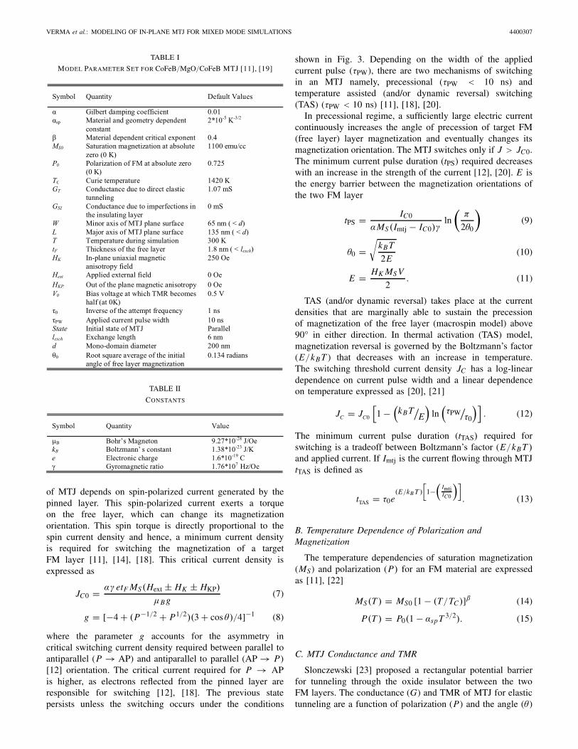
where the parameter g accounts for the asymmetry incritical switching current density required between parallel toantiparallel (P → AP) and antiparallel to parallel (AP → P)[12] orientation. The critical current required for P → APis higher, as electrons reflected from the pinned layer areresponsible for switching [12], [18]. The previous statepersists unless the switching occurs under the conditions
shown in Fig. 3. Depending on the width of the appliedcurrent pulse (τPW), there are two mechanisms of switchingin an MTJ namely, precessional (τPW < 10 ns) andtemperature assisted (and/or dynamic reversal) switching(TAS) (τPW < 10 ns) [11], [18], [20].
In precessional regime, a sufficiently large electric currentcontinuously increases the angle of precession of target FM(free layer) layer magnetization and eventually changes itsmagnetization orientation. The MTJ switches only if J > JC0.The minimum current pulse duration (tPS) required decreaseswith an increase in the strength of the current [12], [20]. E isthe energy barrier between the magnetization orientations ofthe two FM layer
tPS = IC0
αMS (Imtj − IC0)γln
(π
2θ0
)(9)
θ0 =√
kB T
2E(10)
E = HK MS V
2. (11)
TAS (and/or dynamic reversal) takes place at the currentdensities that are marginally able to sustain the precessionof magnetization of the free layer (macrospin model) above90° in either direction. In thermal activation (TAS) model,magnetization reversal is governed by the Boltzmann’s factor(E/kB T ) that decreases with an increase in temperature.The switching threshold current density JC has a log-lineardependence on current pulse width and a linear dependenceon temperature expressed as [20], [21]
JC = JC0
[1 −
(kB T/
E
)ln
(τPW
/τ0
)]. (12)
The minimum current pulse duration (tTAS) required forswitching is a tradeoff between Boltzmann’s factor (E/kB T )and applied current. If Imtj is the current flowing through MTJtTAS is defined as
tTAS = τ0e(E/kB T )
[1−
(ImtjIC0
)]
. (13)
B. Temperature Dependence of Polarization andMagnetization
The temperature dependencies of saturation magnetization(MS) and polarization (P) for an FM material are expressedas [11], [22]
MS(T ) = MS0 [1 − (T/TC)]β (14)
P(T ) = P0(1 − αspT 3/2). (15)
C. MTJ Conductance and TMR
Slonczewski [23] proposed a rectangular potential barrierfor tunneling through the oxide insulator between the twoFM layers. The conductance (G) and TMR of MTJ for elastictunneling are a function of polarization (P) and the angle (θ )
4400307 IEEE TRANSACTIONS ON MAGNETICS, VOL. 50, NO. 8, AUGUST 2014
Fig. 3. MTJ switching mechanism.
between the magnetization orientations of the two ferromag-netic layers as proposed by the Julliere model [18], [24]
G(θ) = GT [1 + P2 cos(θ)] + GSI (16)
TMR(T ) = 2P2
1 − P2 + GSIGT
. (17)
D. Bias Voltage Dependence of TMR
TMR decreases with the increase in bias voltage (V )which is generally modeled by a fitting function [11], [18]expressed as
TMR(T, V ) = TMR0(T )
1 +(
VV0
)2 . (18)
IV. APPLICABILITY OF THE MACROSPIN APPROXIMATION
The macrospin monodomain approximation is valid onlywhen the FM layers (pinned and free) are in single-domainstate. It does not account for inhomogeneous magnetizationstate such as multidomain or vortex state [25]. Hence, onemust ensure that the macrospin approximation holds beforeusing the model for hybrid MTJ/FET design. In this section,physical limitations of geometry and current density arementioned to ensure the applicability of the model.
The single-domain state of magnetization is favorable atdimensions, which scale with the exchange length lexch. Thesingle-domain magnetization is perfectly stable if thickness isless than exchange length. At higher thickness, the exchangeenergy becomes less dominant and single-domain state maynot be energetically stable [25], [26]. The exchange length isexpressed as
lexch =√
2A
μ0 M2S
(19)
where A is the exchange constant and MS is the magnetization.The monodomain diameter d is of the size up to which
magnetic layer has a single-domain state. The diameterdepends on anisotropy and magnetostatic energies definedas [25]
d = λ
(Eanisotropy
Edipole
)1/2
(20)
where λ is domain wall width (Néel wall dominates in thinfilms), Eanisotropy is the anisotropy energy, and Edipole is the
TABLE III
MICROMAGNETIC SIMULATION RESULTS
magnetostatic energy. The horizontal dimensions (W and L)should be kept less than the monodomain diameter.
At the current density greater than 1011 Am−2, one cannotbe sure of the magnetization state. STT at high currentdensities can excite incoherent spin waves and the switchingprocess becomes complicated involving inhomogeneous mag-netization [27], [28]. Hence operation current density must beless than 1011 Am−2.
Micromagnetic simulations are carried out on Magpar [30]to ensure the applicability of monodomain approximationfor parameters given in Table I. The exchange length andmonodomain diameter are determined through energy calcu-lations. The results are shown in Table III and it is evidentthat monodomain approximation limits are met for MTJ withparameters given in Table I.
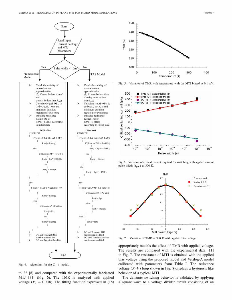
V. ALGORITHM
The model includes two separate submodels for preces-sional and temperature assisted switching (TAS) followed byif–else nest that acts as an arbiter of resistance switching.Precessional model is used when applied current pulse width(τPW ≤ 10 ns) is less than 10 ns. However, at higherpulse width (τPW > 10 ns), the TAS model is used. Thecritical switching currents are calculated according to (7) and(12) for precessional switching and TAS, respectively. Theminimum duration required for switching is calculated fromeither (9) or (13) based on the regime of switching. Thevalue of TMR is calculated according to temperature andapplied bias voltage. The resistance is initialized through atemporary variable Rtemp according to the initial state inputparameter (State). Rtemp is initialized either with P resistancefor State = 0 or with AP resistance for State = 1. Once theresistance is determined, the value Rmtj is assigned to dc andtransient matrices (both Jacobian and RHS). The algorithmwith the if-else nest is shown in Fig. 4.
VI. MODEL VALIDATION
The model is validated by mixed-mode and single MTJdevice simulations on Sentaurus TCAD. Furthermore, theresults of proposed model are compared with the experi-mentally fabricated MTJs [11], [31] and with the previouslyproposed Verilog-A model of in-plane MTJs [12]. The para-meters used for simulation have been mentioned wheneverthere is a change from the default parameters mentioned inTable I.
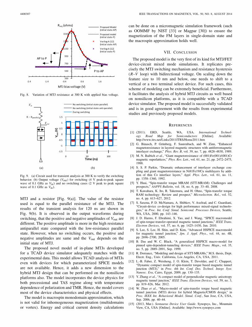
The variation of TMR with temperature is shown in Fig. 5for elastic spin tunneling (GSI = 0) with P0 = 0.641. Thedependence of critical current on applied pulse width for TASregime is analyzed with the Boltzmann’s factor (E/K B T ) set
VERMA et al.: MODELING OF IN-PLANE MTJ FOR MIXED MODE SIMULATIONS 4400307
Fig. 4. Algorithm for the C++ model.
to 22 [8] and compared with the experimentally fabricatedMTJ [31] (Fig. 6). The TMR is analyzed with appliedvoltage (P0 = 0.738). The fitting function expressed in (18)
Fig. 5. Variation of TMR with temperature with the MTJ biased at 0.1 mV.
Fig. 6. Variation of critical current required for switching with applied currentpulse width (τPW ) at 300 K.
Fig. 7. Variation of TMR at 300 K with applied bias voltage.
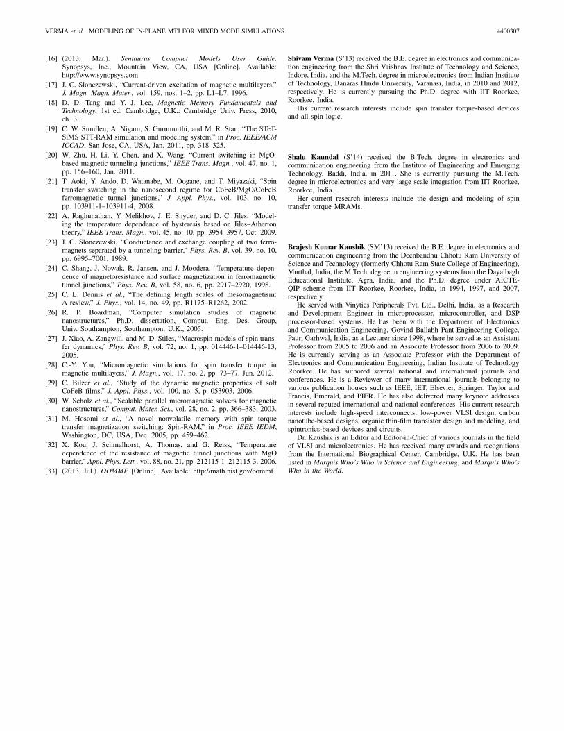
appropriately models the effect of TMR with applied voltage.The results are compared with the experimental data [11]in Fig. 7. The resistance of MTJ is obtained with the appliedbias voltage using the proposed model and Verilog-A modelcalibrated with parameters from Table I. The resistancevoltage (R–V ) loop shown in Fig. 8 displays a hysteresis likebehavior of a typical MTJ.
The dynamic switching behavior is validated by applyinga square wave to a voltage divider circuit consisting of an
4400307 IEEE TRANSACTIONS ON MAGNETICS, VOL. 50, NO. 8, AUGUST 2014
Fig. 8. Variation of MTJ resistance at 300 K with applied bias voltage.
Fig. 9. (a) Circuit used for transient analysis at 300 K to verify the switchingbehavior. (b) Output voltage (Vout) for switching (4 V peak-to-peak squarewave of 0.1 GHz as Vin) and no switching cases (2 V peak to peak squarewave of 0.1 GHz as Vin).
MTJ and a resistor [Fig. 9(a)]. The value of the resistorused is equal to the parallel resistance of the MTJ. Theresults of the transient analysis for 120 ns are shown inFig. 9(b). It is observed in the output waveforms duringswitching, that the positive and negative amplitudes of Vout aredifferent. The positive amplitude is more in the high resistanceantiparallel state compared with the low-resistance parallelstate. However, when no switching occurs, the positive andnegative amplitudes are same and the Vout depends on theinitial state of MTJ.
The proposed novel model of in-plane MTJs developedfor a TCAD device simulator adequately matches with theexperimental data. This model allows TCAD analysis of MTJseven with devices for which parameterized SPICE modelsare not available. Hence, it adds a new dimension to thehybrid MTJ design that can be performed on the nonsiliconplatforms also. The model incorporates the device physics forboth precessional and TAS regime along with temperaturedependence of polarization and TMR. Hence, the model coversmost of the device characteristics and physical effects.
The model is macrospin monodomain approximation, whichis not valid for inhomogeneous magnetization (multidomainsor vortex). Energy and critical current density calculations
can be done on a micromagnetic simulation framework (suchas OOMMF by NIST [33] or Magpar [30]) to ensure themagnetization of the FM layers in single-domain state andthe macrospin approximation holds well.
VII. CONCLUSION
The proposed model is the very first of its kind for MTJ/FETdevice-circuit mixed mode simulations. It replicates pre-cisely the MTJ switching mechanism and resistance hysteresis(R–V loop) with bidirectional voltage. On scaling down thefeature size to 10 nm and below, one needs to shift to avertical or a two terminal select device. For such cases, thisscheme of modeling can be extremely beneficial. Furthermore,it facilitates the analysis of hybrid MTJ circuits as well basedon nonsilicon platforms, as it is compatible with a TCADdevice simulator. The proposed model is successfully validatedand is in good agreement with the results from experimentalstudies and previously proposed models.
REFERENCES
[1] (2011). ERD, Seattle, WA, USA. International Technol-ogy Road Map for Semiconductors [Online]. Available:http://www.itrs.net/Links/2011ITRS/Home2011.htm
[2] G. Binasch, P. Grünberg, F. Saurenbach, and W. Zinn, “Enhancedmagnetoresistance in layered magnetic structures with antiferromagneticinterlayer exchange,” Phys. Rev. B, vol. 39, no. 7, pp. 4828–4830, 1989.
[3] M. N. Baibich et al., “Giant magnetoresistance of (001)Fe(001)/(001)Crmagnetic superlattices,” Phys. Rev. Lett., vol. 61, no. 21, pp. 2472–2475,1988.
[4] S. S. P. Parkin, “Dramatic enhancement of interlayer exchange cou-pling and giant magnetoresistance in Ni81Fe19/Cu multilayers by addi-tion of thin Co interface layers,” Appl. Phys. Lett., vol. 61, no. 11,pp. 1358–1360, 1992.
[5] Y. Huai, “Spin-transfer torque MRAM (STT-MRAM): Challenges andprospects,” AAPPS Bulletin, vol. 18, no. 6, pp. 33–40, 2008.
[6] T. Kawahara, K. Ito, R. Takemura, and H. Ohno, “Spin-transfer torqueRAM technology: Review and prospect,” Microelectron. Rel., vol. 52,no. 4, pp. 613–627, 2012.
[7] S. Saxena, P. D. McNamara, A. Shibkov, V. Axelrad, and C. Guardiani,“Circuit-device co-design for high performance mixed-signal technolo-gies,” in Proc. Int. Conf. Simul. Semicond. Processes Devices, Seattle,WA, USA, 2000, pp. 143–146.
[8] J. D. Harms, F. Ebrahimi, X. Yao, and J. Wang, “SPICE macromodelof spin-torque-transfer-operated magnetic tunnel junctions,” IEEE Trans.Electron Devices, vol. 57, no. 6, pp. 1425–1430, Jun. 2010.
[9] S. Lee, S. Lee, H. Shin, and D. Kim, “Advanced HSPICE macromodelfor magnetic tunnel junction,” Jpn. J. Appl. Phys., vol. 44, no. 4B,pp. 2696–2700, 2005.
[10] B. Das and W. C. Black, “A generalized HSPICE macro-model forpinned spin-dependent-tunneling devices,” IEEE Trans. Magn., vol. 35,no. 5, pp. 2889–2891, Sep. 1999.
[11] R. Dorrance, “Modeling and design of STT-MRAMs,” M.S. thesis, Dept.Electr. Eng., Univ. California, Los Angeles, CA, USA, 2011.
[12] L.-B. Faber, Z. Weisheng, J. O. Klein, T. Devolder, and C. Chappert,“Dynamic compact model of spin-transfer torque based magnetic tunneljunction (MTJ),” in Proc. 4th Int. Conf. Des. Technol. Integr. Syst.Nanosc. Era, Cairo, Egypt, 2009, pp. 130–135.
[13] Y. Zhang et al., “A compact model of perpendicular magnetic anisotropymagnetic tunnel junction,” IEEE Trans. Electron Devices, vol. 59, no. 3,pp. 819–826, Mar. 2012.
[14] W. Zhao et al., “Macro-model of spin-transfer torque based magnetictunnel junction (MTJ) device for hybrid Magnetic/CMOS design,” inProc. IEEE Int. Behavioral Model. Simul. Conf., San Jose, CA, USA,Sep. 2006, pp. 40–44.
[15] (2013, Mar.). Sentaurus Device User Guide. Synopsys, Inc., MountainView, CA, USA [Online]. Available: http://www.synopsys.com
VERMA et al.: MODELING OF IN-PLANE MTJ FOR MIXED MODE SIMULATIONS 4400307
[16] (2013, Mar.). Sentaurus Compact Models User Guide.Synopsys, Inc., Mountain View, CA, USA [Online]. Available:http://www.synopsys.com
[17] J. C. Slonczewski, “Current-driven excitation of magnetic multilayers,”J. Magn. Magn. Mater., vol. 159, nos. 1–2, pp. L1–L7, 1996.
[18] D. D. Tang and Y. J. Lee, Magnetic Memory Fundamentals andTechnology, 1st ed. Cambridge, U.K.: Cambridge Univ. Press, 2010,ch. 3.
[19] C. W. Smullen, A. Nigam, S. Gurumurthi, and M. R. Stan, “The STeT-SiMS STT-RAM simulation and modeling system,” in Proc. IEEE/ACMICCAD, San Jose, CA, USA, Jan. 2011, pp. 318–325.
[20] W. Zhu, H. Li, Y. Chen, and X. Wang, “Current switching in MgO-based magnetic tunneling junctions,” IEEE Trans. Magn., vol. 47, no. 1,pp. 156–160, Jan. 2011.
[21] T. Aoki, Y. Ando, D. Watanabe, M. Oogane, and T. Miyazaki, “Spintransfer switching in the nanosecond regime for CoFeB/MgO/CoFeBferromagnetic tunnel junctions,” J. Appl. Phys., vol. 103, no. 10,pp. 103911-1–103911-4, 2008.
[22] A. Raghunathan, Y. Melikhov, J. E. Snyder, and D. C. Jiles, “Model-ing the temperature dependence of hysteresis based on Jiles–Athertontheory,” IEEE Trans. Magn., vol. 45, no. 10, pp. 3954–3957, Oct. 2009.
[23] J. C. Slonczewski, “Conductance and exchange coupling of two ferro-magnets separated by a tunneling barrier,” Phys. Rev. B, vol. 39, no. 10,pp. 6995–7001, 1989.
[24] C. Shang, J. Nowak, R. Jansen, and J. Moodera, “Temperature depen-dence of magnetoresistance and surface magnetization in ferromagnetictunnel junctions,” Phys. Rev. B, vol. 58, no. 6, pp. 2917–2920, 1998.
[25] C. L. Dennis et al., “The defining length scales of mesomagnetism:A review,” J. Phys., vol. 14, no. 49, pp. R1175–R1262, 2002.
[26] R. P. Boardman, “Computer simulation studies of magneticnanostructures,” Ph.D. dissertation, Comput. Eng. Des. Group,Univ. Southampton, Southampton, U.K., 2005.
[27] J. Xiao, A. Zangwill, and M. D. Stiles, “Macrospin models of spin trans-fer dynamics,” Phys. Rev. B, vol. 72, no. 1, pp. 014446-1–014446-13,2005.
[28] C.-Y. You, “Micromagnetic simulations for spin transfer torque inmagnetic multilayers,” J. Magn., vol. 17, no. 2, pp. 73–77, Jun. 2012.
[29] C. Bilzer et al., “Study of the dynamic magnetic properties of softCoFeB films,” J. Appl. Phys., vol. 100, no. 5, p. 053903, 2006.
[30] W. Scholz et al., “Scalable parallel micromagnetic solvers for magneticnanostructures,” Comput. Mater. Sci., vol. 28, no. 2, pp. 366–383, 2003.
[31] M. Hosomi et al., “A novel nonvolatile memory with spin torquetransfer magnetization switching: Spin-RAM,” in Proc. IEEE IEDM,Washington, DC, USA, Dec. 2005, pp. 459–462.
[32] X. Kou, J. Schmalhorst, A. Thomas, and G. Reiss, “Temperaturedependence of the resistance of magnetic tunnel junctions with MgObarrier,” Appl. Phys. Lett., vol. 88, no. 21, pp. 212115-1–212115-3, 2006.
[33] (2013, Jul.). OOMMF [Online]. Available: http://math.nist.gov/oommf
Shivam Verma (S’13) received the B.E. degree in electronics and communica-tion engineering from the Shri Vaishnav Institute of Technology and Science,Indore, India, and the M.Tech. degree in microelectronics from Indian Instituteof Technology, Banaras Hindu University, Varanasi, India, in 2010 and 2012,respectively. He is currently pursuing the Ph.D. degree with IIT Roorkee,Roorkee, India.
His current research interests include spin transfer torque-based devicesand all spin logic.
Shalu Kaundal (S’14) received the B.Tech. degree in electronics andcommunication engineering from the Institute of Engineering and EmergingTechnology, Baddi, India, in 2011. She is currently pursuing the M.Tech.degree in microelectronics and very large scale integration from IIT Roorkee,Roorkee, India.
Her current research interests include the design and modeling of spintransfer torque MRAMs.
Brajesh Kumar Kaushik (SM’13) received the B.E. degree in electronics andcommunication engineering from the Deenbandhu Chhotu Ram University ofScience and Technology (formerly Chhotu Ram State College of Engineering),Murthal, India, the M.Tech. degree in engineering systems from the DayalbaghEducational Institute, Agra, India, and the Ph.D. degree under AICTE-QIP scheme from IIT Roorkee, Roorkee, India, in 1994, 1997, and 2007,respectively.
He served with Vinytics Peripherals Pvt. Ltd., Delhi, India, as a Researchand Development Engineer in microprocessor, microcontroller, and DSPprocessor-based systems. He has been with the Department of Electronicsand Communication Engineering, Govind Ballabh Pant Engineering College,Pauri Garhwal, India, as a Lecturer since 1998, where he served as an AssistantProfessor from 2005 to 2006 and an Associate Professor from 2006 to 2009.He is currently serving as an Associate Professor with the Department ofElectronics and Communication Engineering, Indian Institute of TechnologyRoorkee. He has authored several national and international journals andconferences. He is a Reviewer of many international journals belonging tovarious publication houses such as IEEE, IET, Elsevier, Springer, Taylor andFrancis, Emerald, and PIER. He has also delivered many keynote addressesin several reputed international and national conferences. His current researchinterests include high-speed interconnects, low-power VLSI design, carbonnanotube-based designs, organic thin-film transistor design and modeling, andspintronics-based devices and circuits.
Dr. Kaushik is an Editor and Editor-in-Chief of various journals in the fieldof VLSI and microlectronics. He has received many awards and recognitionsfrom the International Biographical Center, Cambridge, U.K. He has beenlisted in Marquis Who’s Who in Science and Engineering, and Marquis Who’sWho in the World.