Embed Size (px)
Citation preview
Modeling, Architecture, andApplications for EmergingMemory TechnologiesYuan Xie
Pennsylvania State University
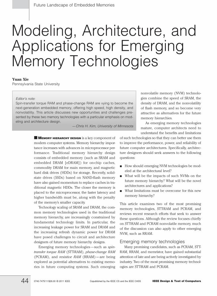
�MEMORY HIERARCHY DESIGN is a key component of
modern computer systems. Memory hierarchy impor-
tance increases with advances in microprocessor per-
formance. Traditional memory hierarchy design
consists of embedded memory (such as SRAM and
embedded DRAM [eDRAM]) for on-chip caches,
commodity DRAM for main memory, and magnetic
hard disk drives (HDDs) for storage. Recently, solid-
state drives (SSDs) based on NAND-flash memory
have also gained momentum to replace caches in tra-
ditional magnetic HDDs. The closer the memory is
placed to the microprocessor, the faster latency and
higher bandwidth must be, along with the penalty
of the memory’s smaller capacity.
Technology scaling of SRAM and DRAM, the com-
mon memory technologies used in the traditional
memory hierarchy, are increasingly constrained by
fundamental technology limits. In particular, the
increasing leakage power for SRAM and DRAM and
the increasing refresh dynamic power for DRAM
have posed challenges to circuit and architecture
designers of future memory hierarchy designs.
Emerging memory technologies��such as spin-
transfer torque RAM (STT-RAM), phase-change RAM
(PCRAM), and resistive RAM (RRAM)��are being
explored as potential alternatives to existing memo-
ries in future computing systems. Such emerging
nonvolatile memory (NVM) technolo-
gies combine the speed of SRAM, the
density of DRAM, and the nonvolatility
of flash memory, and so become very
attractive as alternatives for the future
memory hierarchies.
As emerging memory technologies
mature, computer architects need to
understand the benefits and limitations
of such technologies so that they can better use them
to improve the performance, power, and reliability of
future computer architectures. Specifically, architec-
ture designers should seek answers to the following
questions:
� How should emerging NVM technologies be mod-
eled at the architectural level?
� What will be the impacts of such NVMs on the
future memory hierarchy? What will be the novel
architectures and applications?
� What limitations must be overcome for this new
memory hierarchy?
This article examines two of the most promising
memory technologies, STT-RAM and PCRAM, and
reviews recent research efforts that seek to answer
these questions. Although the review focuses chiefly
on STT-RAM and PCRAM nonvolatile memory, much
of the discussion can also apply to other emerging
NVM, such as RRAM.
Emerging memory technologiesMany promising candidates, such as PCRAM, STT-
RAM, RRAM, and memristor, have gained substantial
attention of late and are being actively investigated by
industry. Two of the most promising memory technol-
ogies are STT-RAM and PCRAM.
Future Landscape of Embedded Memories
Editor’s note:
Spin-transfer torque RAM and phase-change RAM are vying to become the
next-generation embedded memory, offering high speed, high density, and
nonvolatility. This article discusses new opportunities and challenges pre-
sented by these two memory technologies with a particular emphasis on mod-
eling and architecture design.
��Chris H. Kim, University of Minnesota
0740-7475/11/$26.00 �c 2011 IEEE Copublished by the IEEE CS and the IEEE CASS IEEE Design & Test of Computers44
[3B2-14] mdt2011010044.3d 13/1/011 15:51 Page 44
STT-RAM is a new type of
magnetic RAM that features
nonvolatility, fast writing and read-
ing speeds (< 10 ns), high pro-
gramming endurance (> 1,015
cycles), and zero standby
power. The storage capability or
programmability of MRAM arises
from a magnetic tunneling junc-
tion (MTJ), in which a thin tun-
neling dielectric��for example,
magnesium oxide (MgO)��is
sandwiched between two ferro-
magnetic layers, as Figure 1
shows. One ferromagnetic layer
(the pinned layer) is designed
to have its magnetization
pinned, whereas the magnetiza-
tion of the other layer (the free
layer) can be flipped by a write
event. An MTJ has a low resis-
tance if the magnetizations of
both the free and the pinned
layers have the same polarity; it
has a high resistance if the mag-
netizations have opposite polarity. Prototype STT-RAM
chips have been demonstrated at recent industry con-
ferences, and commercial MRAM products have been
launched by companies such as Everspin and NEC.
PCRAM technology is based on a chalcogenide
alloy, typically Ge2Sb2Te5 (GST) material. PCRAM’s
data storage capability is achieved from the resis-
tance differences between an amorphous (high resis-
tance) and crystalline (low resistance) phase of the
chalcogenide-based material. In set operations, the
phase-change material is crystallized by applying an
electrical pulse that heats a significant portion of
the cell above its crystallization temperature. In
reset operations, a larger electrical current is applied
and then abruptly cut off to melt and then quench the
material, leaving it in an amorphous state.
Compared to STT-RAM, PCRAM is even denser,
with an approximate cell area of 6 to 12F2, where F
is the feature size. In addition, phase-change material
has a key advantage with its excellent scalability
within current CMOS fabrication methodologies, fea-
turing continuous density improvement. Many
PCRAM prototypes have been demonstrated by, for
example, Hitachi, Samsung, STMicroelectronics,
and Numonyx.
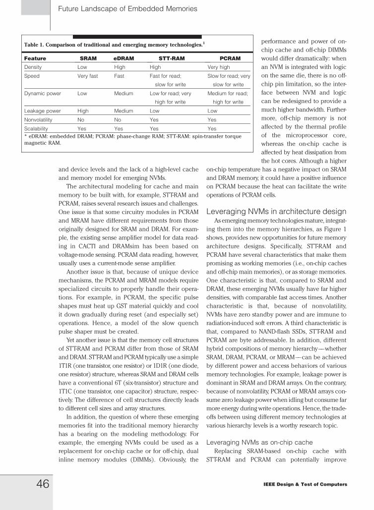
Table 1 shows the comparison of STT-RAM and
PCRAM with conventional memory technologies
used in traditional memory hierarchies.
ModelingTo assist in the architecture-level and system-level
design space exploration of SRAM- or DRAM-based
cache and memory, various modeling tools have
been developed during the past decade. For example,
CACTI (cache access and cycle time) and DRAMsim
(DRAM memory simulator) have become widely
used in the computer architecture community to esti-
mate the speed, power, and area parameters of SRAM
and DRAM caches and main memory.
Similarly, new models have been developed so
that computer architects can explore new design
opportunities at the architecture and system levels.
An STT-RAM-based cache model,2,3 and a PCRAM-
based cache-memory model,4 have been recently
developed at the architecture level. Such models
extract all important parameters, including access
latency, dynamic access power, leakage power, die
area, and I/O bandwidth, to facilitate architecture-
level analysis. The models also bridge the gap be-
tween the abundant research activities at the process
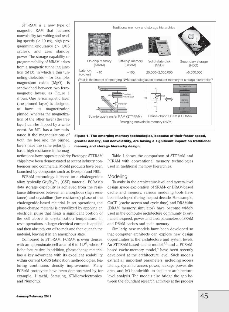
On-chip memory(SRAM)
Off-chip memory(DRAM)
Secondary storage(HDD)
~10 ~100Latency:(cycles)
>5,000,000
Solid-state disk(SSD)
25,000~2,000,000
Phase-change RAM (PCRAM)
Traditional memory and storage hierarchies
Spin-torque-transfer RAM (STT-RAM)
Emerging nonvolatile memory (NVM)
What is the impact of emerging NVM technologies on computer memory or storage hierarchies?
GST
BL
WL
Top electrode
GST
Heater
Substrate
Bottomelectrode
N+
MTJ Free layerPinned layer
Transistor
Wordline
Source line
Bitline
Figure 1. The emerging memory technologies, because of their faster speed,
greater density, and nonvolatility, are having a significant impact on traditional
memory and storage hierarchy design.
45January/February 2011
[3B2-14] mdt2011010044.3d 13/1/011 15:51 Page 45
and device levels and the lack of a high-level cache
and memory model for emerging NVMs.
The architectural modeling for cache and main
memory to be built with, for example, STT-RAM and
PCRAM, raises several research issues and challenges.
One issue is that some circuitry modules in PCRAM
and MRAM have different requirements from those
originally designed for SRAM and DRAM. For exam-
ple, the existing sense amplifier model for data read-
ing in CACTI and DRAMsim has been based on
voltage-mode sensing. PCRAM data reading, however,
usually uses a current-mode sense amplifier.
Another issue is that, because of unique device
mechanisms, the PCRAM and MRAM models require
specialized circuits to properly handle their opera-
tions. For example, in PCRAM, the specific pulse
shapes must heat up GST material quickly and cool
it down gradually during reset (and especially set)
operations. Hence, a model of the slow quench
pulse shaper must be created.
Yet another issue is that the memory cell structures
of STT-RAM and PCRAM differ from those of SRAM
and DRAM. STT-RAM and PCRAM typically use a simple
1T1R (one transistor, one resistor) or 1D1R (one diode,
one resistor) structure, whereas SRAM and DRAM cells
have a conventional 6T (six-transistor) structure and
1T1C (one transistor, one capacitor) structure, respec-
tively. The difference of cell structures directly leads
to different cell sizes and array structures.
In addition, the question of where these emerging
memories fit into the traditional memory hierarchy
has a bearing on the modeling methodology. For
example, the emerging NVMs could be used as a
replacement for on-chip cache or for off-chip, dual
inline memory modules (DIMMs). Obviously, the
performance and power of on-
chip cache and off-chip DIMMs
would differ dramatically: when
an NVM is integrated with logic
on the same die, there is no off-
chip pin limitation, so the inter-
face between NVM and logic
can be redesigned to provide a
much higher bandwidth. Further-
more, off-chip memory is not
affected by the thermal profile
of the microprocessor core,
whereas the on-chip cache is
affected by heat dissipation from
the hot cores. Although a higher
on-chip temperature has a negative impact on SRAM
and DRAM memory, it could have a positive influence
on PCRAM because the heat can facilitate the write
operations of PCRAM cells.
Leveraging NVMs in architecture designAs emerging memory technologies mature, integrat-
ing them into the memory hierarchies, as Figure 1
shows, provides new opportunities for future memory
architecture designs. Specifically, STT-RAM and
PCRAM have several characteristics that make them
promising as working memories (i.e., on-chip caches
and off-chip main memories), or as storage memories.
One characteristic is that, compared to SRAM and
DRAM, these emerging NVMs usually have far higher
densities, with comparable fast access times. Another
characteristic is that, because of nonvolatility,
NVMs have zero standby power and are immune to
radiation-induced soft errors. A third characteristic is
that, compared to NAND-flash SSDs, STT-RAM and
PCRAM are byte addressable. In addition, different
hybrid compositions of memory hierarchy��whether
SRAM, DRAM, PCRAM, or MRAM��can be achieved
by different power and access behaviors of various
memory technologies. For example, leakage power is
dominant in SRAM and DRAM arrays. On the contrary,
because of nonvolatility, PCRAM or MRAM arrays con-
sume zero leakage power when idling but consume far
more energy during write operations. Hence, the trade-
offs between using different memory technologies at
various hierarchy levels is a worthy research topic.
Leveraging NVMs as on-chip cache
Replacing SRAM-based on-chip cache with
STT-RAM and PCRAM can potentially improve
Future Landscape of Embedded Memories
Table 1. Comparison of traditional and emerging memory technologies.1
Feature SRAM eDRAM STT-RAM PCRAM
Density Low High High Very high
Speed Very fast Fast Fast for read;
slow for write
Slow for read; very
slow for write
Dynamic power Low Medium Low for read; very
high for write
Medium for read;
high for write
Leakage power High Medium Low Low
Nonvolatility No No Yes Yes
Scalability Yes Yes Yes Yes
* eDRAM: embedded DRAM; PCRAM: phase-change RAM; STT-RAM: spin-transfer torque
magnetic RAM.
46 IEEE Design & Test of Computers
[3B2-14] mdt2011010044.3d 13/1/011 15:51 Page 46
performance and reduce power consumption. With
larger on-chip cache capacity, because of its higher
density, STT-RAM- and PCRAM-based on-chip cache
can help reduce the cache miss rate, which helps im-
prove performance. Zero-standby leakage can also
help reduce power consumption. On the other hand,
longer write latency of such NVM-based caches could
incur performance degradation and offset any possible
benefits from the reduced cache miss rate. Although
PCRAM is much denser than SRAM, its limited endur-
ance makes directly using PCRAM as on-chip caches,
which have highly frequent accesses, unaffordable.
Dong et al. investigated the performance and
power benefits of STT-RAM for single-core processors.2
Their research demonstrated that an STT-RAM-based
level-2 (L2) cache could improve performance while
simultaneously reducing power consumption by
more than 70%. Sun et al. demonstrated the benefits
of using an STT-RAM-based shared L2 cache for multi-
core processors.3 Their simulation results shows that
the optimized MRAM L2 cache improves performance
by 4.91% and reduces power by 73.5% compared to a
conventional SRAM L2 cache with a similar area.
Wu et al.1 studied a number of different hybrid-
cache architectures (HCAs) composed of SRAM,
eDRAM, STT-RAM, and PCRAM for an IBM Power7
cache architecture. These researchers also explored
the potential of hardware support for intra-cache
data movement and power consumption manage-
ment within HCA caches. Under the same area con-
straint across a collection of 30 workloads, Wu et al.
found that such an aggressive hybrid-cache design
provides a 10% to 16% performance improvement
over the baseline design with a level-3, SRAM-only
cache design, and achieves up to a 72% reduction
in power consumption.
Leveraging NVMs as main memory
There have been abundant recent investigations
on using PCRAM as a replacement for the current
DRAM-based main memory architecture. Lee
et al.,5 for example, demonstrated that a pure
PCRAM-based main memory architecture imple-
mentation is about 1.6� slower and requires 2.2�as much energy as a DRAM-based main memory,
mainly because of the overhead of write opera-
tions. Lee et al. proposed to redesign the PCRAM
buffer organizations, with narrow buffers to mitigate
high-energy PCM writes. Also, with multiple buffer
rows the architecture can exploit locality to
coalesce writes, hiding their latency and energy,
such that the performance is only 1.2� slower, with
similar energy consumption, than a DRAM-based
system.
Qureshi et al.6 proposed a main memory system
consisting of PCM storage coupled with a small
DRAM buffer, so that it can leverage the latency ben-
efits of DRAM and the capacity benefits of PCM. Such
a memory architecture could reduce page faults by
5� and provide a speedup of 3�.
A similar study conducted by Zhou et al.7 demon-
strated that the PCRAM-based main memory consumes
only 65% of the total energy of the DRAM main mem-
ory with the same capacity, and the energy-delay prod-
uct is reduced by 60%, with various techniques to
mitigate the overhead of write operations. Cumula-
tively, this research demonstrates the feasibility of
using PCRAM as main memory in the near future.
Leveraging NVM to improve NAND-flash SSDs
NAND-flash memory has been widely adopted by
various applications such as laptops and mobile
phones. In addition, because of its better perfor-
mance compared to traditional HDDs, NAND-flash
memory has been proposed for use as a cache in
HDDs, or as an HDD replacement in some applica-
tions. However, one well-known limitation of NAND-
flash memory is the ‘‘erase before write’’ requirement.
It cannot update the data by directly overwriting it.
Instead, a time-consuming erase operation must be
performed before the overwriting. To complicate mat-
ters, the erase operation cannot be performed selec-
tively on a particular data item or page but can
only be done for a large block called the ‘‘erase
unit.’’ Because the size of an erase unit (typically
128 Kbytes) is much larger than that of a page (typi-
cally 512 bytes to 8 Kbytes), even a small update to
a single page requires all the pages within the erase
unit to be erased and written again.
Compared to NAND-flash memory, PCRAM and
STT-RAM have the advantages of random access
and direct in-place updating. Consequently, Sun
et al.8 have proposed using a hybrid storage architec-
ture that combines the advantages of NAND-flash
memory and PCRAM and STT-RAM. Such a hybrid
storage architecture uses PCRAM as the log region
for NAND-flash.
Such a hybrid architecture has four advantages.
First, it has the ability of ‘‘in-place updating,’’ which
can significantly improve the usage efficiency of the
47January/February 2011
[3B2-14] mdt2011010044.3d 13/1/011 15:51 Page 47

log region by eliminating the out-of-date log data. Sec-
ond, the fine-grained access of PCRAM can greatly re-
duce the read traffic from SSDs to main memory.
Third, the energy consumption of the storage system
is reduced as the overhead of writing and reading log
data is decreased with the PCRAM log region. Fourth,
the lifetime of the NAND-flash memory in the hybrid
storage could increase if the number of erase opera-
tions is reduced.
Enabling fault-tolerant exascale computing
As a result of continuously reduced feature size,
reduced supply voltage, and increased on-chip density,
tomorrow’s computer systems are projected to be
more susceptible to both hard and transient errors.
Compared to SRAM and DRAM memory, PCRAM
and STT-RAM memory have unique features such as
nonvolatility and resilience to soft errors. The applica-
tion of such unique features could enable a novel ar-
chitecture design for applications that address the
reliability challenges for future exascale computing.
For example, a checkpointing or rollback scheme,
in which the processor takes frequent checkpoints at
certain intervals and stores the checkpoints on a
hard disk, is one of the most common approaches
to ensure the fault tolerance of a computing system.
In today’s petascale, massively parallel processing
(MPP) systems, such traditional checkpointing to a
hard disk could incur a large performance overhead
and is not a scalable solution for future exascale com-
puting. By way of a possible solution, Dong et al. have
proposed three variants of PCRAM-based hybrid
checkpointing schemes, which reduce the checkpoint
overhead and offer a smooth transition from the con-
ventional pure-HDD checkpoint to the ideal 3D
PCRAM mechanism.9 With a 3D PCRAM approach,
multiple layers of PCRAM memory are stacked
atop DRAM memory, integrated with the emerging
3D integration technology. With a massive memory
bandwidth provided by the through-silicon vias
(TSVs) enabled by 3D integration, fast and high-
bandwidth local checkpointing can be realized.
The proposed pure 3D PCRAM-based mechanism
can ultimately take checkpoints with an overhead
of less than 4% on a projected exascale system.
Mitigation techniques for STT-RAM/PCRAM
The benefits of using these emerging memory
technologies in computer system design can be
achieved only with mitigation techniques that help
address the NVMs’ inherent disadvantages related to
the write operations. One disadvantage is that, be-
cause of the memory’s nonvolatility feature, it usually
takes much longer and requires more energy for
writes than for reads. A second drawback is that
some NVMs, such as PCRAM, have a problem with
wearout (lifetime reliability), which is one of the
major concerns of using it as working memory rather
than a storage class memory. Consequently, introduc-
ing NVMs into designs with the current memory hier-
archy gives rise to new opportunities but also presents
new challenges. Several mitigation techniques are
possible to help address these disadvantages.
NVM latency and energy overhead
mitigation techniques
To use emerging NVMs as cache and memory, sev-
eral design issues must be solved, most importantly
the performance and energy overhead requirement
for write operations. An NVM has a more stable mech-
anism for storing data, compared to the volatility of
SRAM and DRAM. Accordingly, NVMs intrinsically
take longer and consume more energy to overwrite
the existing data. If we directly replace SRAM caches
with a PCRAM or STT-RAM cache, the long latency
and high energy consumption in writes could offset
the performance and power benefits, and even result
in degradation when the cache write intensity is high.
The following approaches, therefore, deserve more
consideration for mitigating the overheads of NVM
write operations.
Hybrid cache or memory architecture. To lever-
age the benefits (such as fast write operations) of
both traditional SRAM and DRAM and those (such as
high density, low leakage, and soft-error resiliency) of
emerging NVMs, a hybrid cache or memory architec-
ture can be used. Two possibilities for this are an STT-
RAM or SRAM hybrid on-chip cache,3 or a PCRAM or
DRAM hybrid main memory.6 In such a hybrid architec-
ture, instead of building a pure STT-RAM-based cache
or a pure PCRAM-based main memory, we could re-
place a portion of the MRAM or PCRAM cells with
SRAM or DRAM elements, respectively. The main pur-
pose is to keep most of the write-intensive data within
SRAM or DRAM, and thus reduce write operations in
an NVM. This solution would reduce dynamic power
consumption and further improve performance. The
major challenges to this architecture are how to
Future Landscape of Embedded Memories
48 IEEE Design & Test of Computers
[3B2-14] mdt2011010044.3d 13/1/011 15:51 Page 48

physically arrange the two different types of memories
and how to migrate data between them.
Novel buffer architecture. The write buffer design
in modern processors works well for SRAM-based
caches, which have approximately equivalent read
and write speeds. The traditional write buffer design,
however, might not be suitable for NVM-based
caches, which feature a large variation between
read and write latencies. As a potential solution,
Sun et al.3 proposed to design a novel write buffer ar-
chitecture to mitigate the write-latency overhead. For
example, in a situation in which a write operation is
followed by several reads, the ongoing write might
block the upcoming reads and thereby degrade per-
formance. The cache write buffer can be improved
to prevent the critical read operations from being
blocked by long writes. A higher priority, for in-
stance, can be assigned to read operations when a
read and write compete. In an extreme condition
when write retirements are always stalled by reads,
the write buffer could become full, which can also
degrade cache performance. How to deal with the
read-write sequence, and investigating whether this
mechanism could be dynamically controlled by the
application are two matters to be resolved. Qureshi
et al. have proposed similar techniques for write can-
cellation and write pausing.10 In addition, Lee et al.5
have proposed to redesign the PCRAM buffer, using
narrow buffers to help mitigate high-energy PCM
writes. Multiple buffer rows can exploit locality to co-
alesce writes, hiding their latency and energy.
Eliminating redundant bit-writes. In a conven-
tional memory access, a write updates an entire
row of memory cells. A large portion of such writes
are redundant. A read-before-write operation can
help identify such redundant bits and cancel those re-
dundant write operations to save energy and reduce
the impact on performance.11
Data inverting. To further reduce the number of
writes to PCRAM cells, a data-inverting scheme,
detailed elsewhere,11,12 can be adopted in the
PCRAM write logic. When new data is written to a
cache block, the old data value is first read, then
the Hamming distance is computed between the
two values. If the calculated Hamming distance is
larger than half of the cache block size, the new
data value is inverted before the store operation. An
extra status bit is set to 1 to denote that the stored
value has been inverted.
Techniques to improve NVM lifetime
Write endurance poses another severe challenge
in PCRAM memory design. State-of-the-art process
technology has demonstrated that the write endur-
ance for PCRAM is around 108 to 109.7 The problem
is further aggravated by the fact that writes to caches
and main memory can be extremely skewed. Conse-
quently, those cells suffering from more frequent write
operations will fail far sooner than the rest.
As just discussed, techniques to reduce the num-
ber of write operations to STT-RAM and PCRAM can
definitely help extend memory lifetime, as well as re-
duce the write energy overhead. In addition to those
techniques, the following schemes can be used to fur-
ther extend memory lifetime.
Wear leveling. Wear leveling, which has been widely
implemented in NAND-flash memory, attempts to work
around the limitations of write endurance by arranging
data access so that write operations can be distributed
evenly across all the storage cells. Wear leveling can
also be applied to PCRAM- and MRAM-based cache
and memory. A range of wear-leveling techniques for
PCRAM have been examined recently.5-7,11,13 Such
wear-leveling techniques include the following:
� Row shifting. A simple shifting scheme can be ap-
plied to evenly distribute writes within a row. The
scheme is implemented through an additional
row shifter along with a shift offset register. On a
read access, data is shifted back before being
passed to the processor.
� Wordline remapping and bitline shifting. These are
used to spread the writes over the memory cells
within a cache block and among cache blocks.
� Segment swapping. Periodically, memory segments
of high and low write accesses are swapped. The
memory controller keeps track of the write counts
of each segment, and keeps a mapping table be-
tween the ‘‘virtual’’ and ‘‘true’’ segment number.
Graceful degradation. In this scheme, the PCRAM
allows continued operation through graceful degra-
dation when hard faults occur.14 The memory pages
that contain hard faults are not discarded. Instead,
they are dynamically formed pairs of complementary
pages that act as a single page of storage, such that
49January/February 2011
[3B2-14] mdt2011010044.3d 13/1/011 15:51 Page 49
the total effective memory capacity is reduced but
the PCRAM lifetime can be improved by up to 40�over conventional error-detection techniques.
RECENT ARCHITECTURAL-LEVEL STUDIES have demon-
strated that emerging memories have great potential
to improve future computer memory architecture
design. Numerous opportunities exist for novel archi-
tectures and applications that these emerging
memory technologies can enable. For example, lever-
aging the on-chip memory’s nonvolatility could
enable many interesting innovations for current
microarchitecture designs, such as instant-(on/off)
pipeline design. With all these initial research efforts,
researchers believe that the emergence of these new
memory technologies will change the landscape of
future memory architecture design. We hope this arti-
cle will serve as a catalyst to accelerate the adoption
of such memories for future systems from both archi-
tecture and system design perspectives. �
AcknowledgmentsThe work in this article was supported in part by
National Science Foundation grants 1017277,
0903432, and by Semiconductor Research Corpora-
tion, Qualcomm, and the US Department of Energy.
�References1. X. Wu et al., ‘‘Hybrid Cache Architecture with Disparate
Memory Technologies,’’ Proc. 36th Int’l Symp. Computer
Architecture (ISCA 09), ACM Press, 2009, pp. 34-45.
2. X. Dong et al., ‘‘Circuit and Microarchitecture Evaluation
of 3D Stacking Magnetic RAM (MRAM) as a Universal
Memory Replacement,’’ Proc. 45th Design Automation
Conf. (DAC 08), ACM Press, 2008, pp. 554-559.
3. G. Sun et al., ‘‘A Novel Architecture of the 3D Stacked
MRAM L2 Cache for CMPs,’’ Proc. 15th Int’l Symp. High
Performance Computer Architecture (HPCA-15), IEEE
CS Press, 2009, pp. 239-249.
4. X. Dong, N. Jouppi, and Y. Xie, ‘‘PCRAMsim: System-
Level Performance, Energy, and Area Modeling for
Phase Change RAM,’’ Proc. Int’l Conf. Computer-Aided
Design (ICCAD 09), ACM Press, 2009, pp. 269-275.
5. B.C. Lee et al., ‘‘Architecting Phase Change Memory as
a Scalable DRAM Alternative,’’ Proc. 36th Int’l Symp.
Computer Architecture (ISCA 09), ACM Press, pp. 2-13.
6. M.K. Qureshi, V. Srinivasan, and J.A. Rivers, ‘‘Scalable
High Performance Main Memory System Using Phase-
Change Memory Technology,’’ Proc. 36th Int’l Symp. Com-
puter Architecture (ISCA 09), ACM Press, 2009, pp. 24-33.
7. P. Zhou et al., ‘‘A Durable and Energy Efficient Main
Memory Using Phase Change Memory Technology,’’
Proc. 36th Int’l Symp. Computer Architecture (ISCA 09),
ACM Press, 2009, pp. 14-23.
8. G. Sun et al., ‘‘A Hybrid Solid-State Storage Architecture
for Performance, Energy Consumption and Lifetime Im-
provement,’’ Proc. 16th Int’l Symp. High-Performance
Computer Architecture (HPCA-16), IEEE CS Press,
2010; doi:10.1109/HPCA.2010.5416650.
9. X. Dong et al., ‘‘Leveraging 3D PCRAM Technologies to
Reduce Checkpoint Overhead for Future Exascale Sys-
tems,’’ Proc. Int’l Conf. High Performance Computing,
Networking, Storage and Analysis (SC 09), IEEE
CS Press, 2009; doi:10.1145/1654059.1654117.
10. M. Qureshi, M. Franceschini, and L. Lastras, ‘‘Improving
Read Performance of Phase Change Memories via Write
Cancellation and Write Pausing,’’ Proc. 16th Int’l Symp.
High-Performance Computer Architecture (HPCA-16),
IEEE CS Press, 2010; doi 10.1109/HPCA.2010.5416645.
11. Y. Joo et al., ‘‘Energy- and Endurance-Aware Design of
Phase Change Memory Caches,’’ Proc. Design, Automa-
tion and Test in Europe Conf. (DATE 10), IEEE CS
Press, 2010, pp. 136-141.
12. S. Cho and H. Lee, ‘‘Flip-N-Write: A Simple Deterministic
Technique to Improve PRAM Write Performance, Energy
and Endurance,’’ Proc. 42nd Ann. Int’l Symp. Microarchi-
tecture (MICRO-42), ACM Press, 2009, pp. 347-357.
13. M. Qureshi et al., ‘‘Enhancing Lifetime and Security of
Phase Change Memories via Start-Gap Wear Leveling,’’
Proc. 42nd Ann. Int’l Symp. Microarchitecture (MICRO-
42), ACM Press, 2009, pp. 14-23.
14. E. Ipek et al., ‘‘Dynamically Replicated Memory: Building
Reliable Systems from Nanoscale Resistive Memories,’’
Proc. Int’l Conf. Architecture Support for Programming
Languages and Operating Systems (ASPLOS 10), ACM
Press, 2010, pp. 3-14.
Yuan Xie is an associate professor in the Computer
Science and Engineering Department at Pennsylvania
State University. His research interests include com-
puter architecture, VLSI design, EDA, and embedded
systems. He has a PhD in electrical engineering from
Princeton University. He is an IEEE senior member
and an ACM member.
�Direct questions and comments about this article to
Yuan Xie, Computer Science and Engineering De-
partment, 354E Information Science Technology
Bldg., Pennsylvania State University, University Park,
PA 16802; [email protected].
Future Landscape of Embedded Memories
50 IEEE Design & Test of Computers
[3B2-14] mdt2011010044.3d 13/1/011 15:51 Page 50

[3B2-14] mdt2011010044.3d 13/1/011 15:51 Page 51