Embed Size (px)
Citation preview

Modeling and optimization of a single-drive push–pullsilicon Mach–Zehnder modulator
Yanyang Zhou,1 Linjie Zhou,1,* Haike Zhu,1 Chiyan Wong,2 Yida Wen,2 Lei Liu,2
Xinwan Li,1 and Jianping Chen1
1State Key Laboratory of Advanced Optical Communication Systems and Networks,Department of Electronic Engineering, Shanghai Jiao Tong University, Shanghai 200240, China
2Transmission Technology Research Department, Huawei Technology Co. Ltd., Shenzhen 518129, China*Corresponding author: [email protected]
Received March 8, 2016; revised June 28, 2016; accepted June 30, 2016;posted July 1, 2016 (Doc. ID 260720); published July 26, 2016
We present an equivalent circuit model for a silicon carrier-depletion single-drive push–pull Mach–Zehndermodulator (MZM) with its traveling wave electrode made of coplanar strip lines. In particular, the partial-capacitance technique and conformal mapping are used to derive the capacitance associated with each layer.The PN junction is accurately modeled with the fringe capacitances taken into consideration. The circuit modelis validated by comparing the calculations with the simulation results. Using this model, we analyze the effectof several key parameters on the modulator performance to optimize the design. Experimental results of MZMsconfirm the theoretical analysis. A 56 Gb/s on–off keying modulation and a 40 Gb/s binary phase-shift keyingmodulation are achieved using the optimized modulator. © 2016 Chinese Laser Press
OCIS codes: (130.0250) Optoelectronics; (230.2090) Electro-optical devices; (230.4110) Modulators;(250.3140) Integrated optoelectronic circuits.http://dx.doi.org/10.1364/PRJ.4.000153
1. INTRODUCTIONIn recent years, the rapid growth of transmission capacity infiber-optic networks has required optical modulators to pos-sess a large electro-optic (EO) bandwidth to transmit opticalsignals at high bit rates. Silicon optical modulators based onthe free carrier plasma dispersion effect have the uniqueadvantage of monolithic integration with microelectroniccircuits on one single chip [1,2]. The carrier-depletion-basedsilicon Mach–Zehnder modulator (MZM) with the travelingwave electrode (TWE) has been widely investigated overthe past decade [3]. Both PN junction and TWE play criticalroles in achieving high-speed and high-efficiency modulation.The PN junction needs to be optimized to interact efficientlywith the waveguide mode while keeping a low optical loss.Many types of PN junctions have been adopted, such as theinterdigitated PN junction [4], the vertical PN junction [5,6],and the PN junction with a compensated region [7,8]. Onthe other hand, the TWE should be designed to have imped-ance match, phase match, and low microwave loss to offer alarger EO bandwidth [9–11]. Coplanar waveguides (CPW) andcoplanar striplines (CPS) are the two major microwave guid-ing structures used in the TWE.
In order to design and optimize the PN junction and TWE,finite-element-method (FEM) simulations, which involve com-plex 2D or 3D device modeling with a fine mesh are routinelyused to ensure a high level of accuracy. However, this methodlacks efficiency because it needs a long time for numericalcalculation and huge computing resources. Moreover, inter-pretation of the simulation results is sometimes difficult with-out a clear physical model. Therefore, it is highly demanded todevelop a more efficient and physically orientated model toguide silicon modulator design. An equivalent circuit model
established based on the device physics can give clear direc-tions for device optimization. Most of the differential-drivesilicon modulators adopt the CPW as the TWE [4,10,12,13],and the corresponding equivalent circuit model has beenbuilt [14]. The analytical model presented in [14] simplifiesthe PN junction and does not take into consideration theeffect of the fringing electric fields and capacitances, whichwas later studied theoretically in [15]. Compared with thedifferential-drive modulators, the single-drive push–pull sili-con modulators with a CPS-type TWE [16–19] feature lowchirp [20], large bandwidth [19], high linearity [21], andsimplified RF interface. The drawback is the increased drivevoltage, which is a shortcoming because low voltage is alwaysrequired to be compatible with CMOS circuits. Nevertheless,such a drive scheme is preferably demanded in implementa-tion of advanced modulation formats such as quadraturephase-shift keying, quadrature amplitude modulation, andN-level pulse amplitude modulation. Hence, it is desired todevelop an equivalent circuit model for the single-drivepush–pull silicon MZM.
In this paper, we present an equivalent circuit model for thecarrier-depletion-based silicon MZM driven by a single-drivepush–pull electrode. The device design is optimized basedon the model. In Section 2, we present the details of the circuitmodel, including the CPS TWE and the PN junction. The keyfeatures of our model are twofold: (1) the model is derivedaccording to the electrical field distribution in the phaseshifter; (2) the model incorporates the microwave loss dueto the doped slab layer, which is eliminated by using seg-mented PN junctions. The derived circuit model is justifiedby comparing with FEM simulations. In Section 3, we usethe circuit model to optimize the TWE and the segmented
Zhou et al. Vol. 4, No. 4 / August 2016 / Photon. Res. 153
2327-9125/16/040153-09 © 2016 Chinese Laser Press
Corrected 27 July 2016

PN junction to enlarge the EO bandwidth while reducing themicrowave loss. The doping concentration is also separatelyoptimized by using FEM simulation to achieve high modula-tion efficiency. In Section 4, we present the measured perfor-mance of the MZMs. The S-parameter measurements showthat the modulator with segmented PN junctions suffers alower microwave loss in the high RF frequency end. TheEO bandwidth of the optimized modulator is 33 GHz at 4 Vreverse bias. On–off keying (OOK) modulation at the dataof 56 Gb/s is realized with an extinction ratio (ER) of 4 dBand a Q-factor of 3.73. Binary phase-shift keying (BPSK)modulation is also realized at 40 Gb/s with the bit error rate(BER) below the forward error correction level.
2. EQUIVALENT CIRCUIT MODELFigure 1(a) shows the cross section of the active arms drivenby the CPS-TWE of the silicon MZM. PN junctions are em-bedded in the silicon-on-insulator rib waveguides. The wave-guide has a widthW rib � 500 nm, a heightHrib � 220 nm, anda remaining slab height Hslab � 90 nm. The PN junction is lo-cated in the waveguide center with a lateral offset Δjun towardthe N-doped side. Highly doped regions are separated fromthe waveguide sidewalls with a distance Sdop to reducefree-carrier absorption loss. The P�� doping regions are con-nected to the signal and ground metal lines of the CPS-TWE,respectively. A DC bias Vb is applied to the middle N�� dopingregion to set the two PN junctions in a reverse bias mode. We
adopt the asymmetric MZI structure because the bias pointneeded for OOK and BPSK modulations can be convenientlyset by tuning the input laser wavelength. Figure 1(b) showsthe calculated electric field distribution of the microwavedrive signal, which is helpful to establish the equivalent circuitmodel. As the electric field is distributed in all layers, we willconsider the contribution of each layer to the entire circuit.
Figure 2(a) shows the equivalent circuit model of the CPS-TWE in each layer. Figure 2(b) depicts the two-port transmis-sion line model where the CPS-TWE can be represented by thecharacteristic impedance (Z) and the propagation constant(γ). In order to achieve a high EO bandwidth, Z should beequal to the source impedance (Zs) and the terminal imped-ance (Zt), eliminating the microwave signal backreflection.Generally, in the conventional microwave communicationsystem, Zt and Zs are 50Ω. The microwave effective refractiveindex (neffw) should be close to the group refractive index ofthe waveguide optical mode (ngo) to synchronize the electricaland optical waves. The microwave attenuation factor (α) is akey parameter to determine the electro–electro (EE) band-width of the TWE. Both neffw and α can be deduced from γ.
Based on the partial-capacitance technique and the con-formal mapping, we can derive the capacitance associatedwith each layer. We use the theoretical derivation in [22] tocalculate the capacitances. The geometrical factor for a con-formal mapped air-filled CPS is defined as follows:
F�ki� �K�ki�K�k0i�
; (1)
k0 �����������������������1 −
�xa
xb
�2
s; (2)
Fig. 1. (a) Cross section of a single-drive push–pull carrier-depletion-based optical modulator. Inset shows the zoom-in of the PN junction.(b) Microwave electrical field distribution in the modulation arms.
Fig. 2. (a) Electrical components contributed by each layer. (b) Two-port network and the equivalent circuit model of the modulator.
154 Photon. Res. / Vol. 4, No. 4 / August 2016 Zhou et al.

ki �
������������������������������1 −
sinh2�πxa2hi
�sinh2
�πxb2hi
�vuuut ; (3)
where K�ki� is the complete elliptic integral of the first kind,ki is the argument of the integral (i � 0, 1, 2, 3, 4) and
k0i ��������������1 − k2i
q, hi is the thickness denoted in Fig. 1(a),
2xa � Gmt is the gap size between the two metal lines, andxb − xa � Wmt is the metal width. The capacitances contrib-uted by each layer can be expressed using the geometricalfactor.
The behavior of the silicon substrate is described by a con-ductor Gsub and a capacitor Csub connected in parallel [23]:
Gsub � 2σsub
�F2�k0�F�k1�
−
F2�k0�F�k2�
�; (4)
Csub � 12ε0εsi
�F2�k0�F�k1�
−
F2�k0�F�k2�
�; (5)
where σsub is the conductivity of the silicon substrate, ε0 is thepermittivity in vacuum, and εsi is the silicon relative permittiv-ity. A capacitor Csub_s is used to represent the capacitancebetween the signal metal strip and the Si substrate, given by
Csub_s � ε0εoxWmt∕h2; (6)
where εox is the silicon dioxide relative permittivity. An aux-iliary capacitor Csub1 is present to make the total capacitanceconverge to Csub at the high-frequency limit [14]. Therefore,we have the following expression:
Csub � Csub_sCsub
Csub � Csub_s� Csub1: (7)
The capacitance of the BOX layer CBOX is given by
CBOX � 12ε0εox
�F2�k0�F�k2�
−
F2�k0�F�k3�
�: (8)
According to [15], the PN junction depletion capacitanceCdep is made of four parts: the ideal depletion capacitanceC∥, the fringe capacitance Cf due to the charges at the centerof the diode, and the fringe capacitances Ccpst and Ccpsb due toextended depletion widths tp;n at the top and bottom surfacesof the waveguide, respectively. These constituent capaci-tances are expressed as
Cdep � C∥ � Cf � Ccpst � Ccpsb; (9)
C∥ � ε0εsiHrib
WD
; (10)
Cf � ε0εoxπ
ln�2π
Hrib
WD
�; (11)
Ccpst;b � ε0εoxK�k0�K�k� ; (12)
k ���������������������������������������������WD�WD � tn � tp��WD � tn��WD � tp�
s; (13)
tp;n � 2WDp;n�εox�π
; (14)
whereWD is the center depletion region width, andWDp;n�εox�is the depletion widths in the p and n sides of the diode calcu-lated using εox. The depletion width WD can be approximatedfrom 1D PN diode model as
WD � WDp �WDn ��������������������������������������������������������������������������������2ε0εsiq
�NA � ND
NAND
��Vj − Vb −
2kBTq
�s;
(15)
where NA;D is the carrier concentration in p∕n regions, Vj isthe built-in potential of the junction, Vb is the bias voltage onthe junction, q is the fundamental electron charge, kB is theBoltzmann constant, and T is the ambient temperature. Theimpedance due to the lightly doped slab and rib sections isgiven by
Rp;n � ρp;n1� jωmρp;nε0εsi
�Sdop
Hslab� Sp;n
Hrib
�; (16)
Sp � W rib
2� Δjun −WDp; (17)
Sn � W rib
2− Δjun −WDn; (18)
ρp;n � 1qμp;nNA;D
; (19)
where μp;n is the mobility of the p, n-doped silicon, and ω is themicrowave frequency.
The capacitance between the two metal vias in the uppercladding layer Cvia is modeled by a parallel plate capacitance:
Cvia � ε0εoxh4∕Gvia: (20)
Similarly, the capacitance formed between the signal andground metal lines is expressed as
Cmt � ε0Tmt∕Gmt: (21)
The capacitance in the air space outside the chip isexpressed as
Cair � ε0F2�k0� −
12ε0
F2�k0�F�k1�
: (22)
At the high microwave frequencies, the longitudinal currentflows along the transmission lines and highly doped slabs [24].The resistance of the slab per unit length, Rslab, is expressed as
Rslab � ρp��
1� jωmρp��ε0εsi
2HslabWp
; (23)
Zhou et al. Vol. 4, No. 4 / August 2016 / Photon. Res. 155

where ρp�� is the conductivity of the P��-doped slabs.In order to reduce the microwave loss due to the doped slab,we can use a segmented PN junction (e.g., a 1 μm long stria-tion undoped in every 10 μm long PN junction) to ensure thatcurrent flows only in the metal strips [25]. This undoped stria-tion forms an extra capacitance in the slab. The capacitanceper unit length, Cslab, is expressed as
Cslab � ε0εsiWpHslab
d
1Λ; (24)
where d is the undoped striation width and Λ is the period ofsegmented PN junction.
The longitudinal current flow in the metal strips is repre-sented as the resistance R in series with the inductance L.According to electrical field distribution in the CPW andCPS structures, the CPS can be regarded as one half ofCPW. The R and L are expressed as
L � 2LCPW; (25)
R � RG � RS � 2RCPW; (26)
where RCPW and LCPW can be calculated by the formulas givenin [26]. The longitude current also flows in the substrate,which is ignored because the resistance of substrate is muchlarger than the highly doped slabs [27].
The above constituent circuit components can be trans-formed to a simple transmission line model with effectivecomponents Reff , Leff , Ceff , Geff , as shown in Fig. 2(b). Thecomplex characteristic impedance Z and the complex propa-gation constant γ are expressed as
Z ������������������������������Reff � jwLeff
Geff � jwCeff
s; (27)
γ � α� jβ ������������������������������������������������������������������Reff � jwLeff��Geff � jwCeff�
p: (28)
The average voltage that drops across the signal andground metal lines is given by [14]
Vavg�ωm� � Vg
�1� ρ1� exp�iβ0L��V� � ρ2V−
�2�exp�γL� � ρ1ρ2 exp�−γL�� ; (29)
V� � exp��i
�−iγ β0�L2
�sin��−iγ β0�L∕2��−iγ β0�L∕2
; (30)
ρ1 �Z − Zs
Z � Zs
; (31)
ρ2 �Zt − Z
Zt � Z; (32)
β0 �ωm
cngo; (33)
where Vg is the drive signal voltage amplitude, ωm is itsmodulation frequency, and Lmt is the length of the TWE.
The average voltage formula in Eq. (29) has taken intoaccount the velocity match, impedance match, and the micro-wave loss. Any velocity mismatch and impedance mismatchwill reduce the accumulated interaction between microwaveand optical wave. Based on the Z and γ, the S-parameters ofthe TWE are expressed as
S21�ωm� � �1� Γs��1� Γt�e−γL; (34)
S11�ωm� � Γs; (35)
where Γs and Γt are reflections at the input and load ends,respectively, given by
Γs �Zin − Zs
Zin � Zs
; (36)
Γt �Zin − Zt
Zin � Zt
; (37)
where Zin is the TWE input impedance, given by
Zin � ZZt − Z tanh�γL�Z − Zt tanh�γL�
: (38)
The voltage useful for modulation is the voltage drop on thePN junctions:
Vdep�ωm� �Vavg�ωm�
1� jω�Rp � Rn�Cdep: (39)
Therefore, the modulator frequency response can beexpressed as the junction voltage normalized to its low-frequency (ω0) value:
m�ωm� �Vdep�ωm�Vdep�ω0�
: (40)
As a first-order approximation, the EO S21 response isdirectly related to m�ωm�. The 3 dB EO bandwidth ω3 dB isreached when m�ω3 dB� � 0.5.
In order to verify the validity of the equivalent circuitmodel, we compare the analytical modeling results with thenumerical simulation results by the commercial softwareCOMSOL Multiphysics, which uses the FEM to solveMaxwell’s equations. The MZM design was described in detailin our previous work [17]. The device parameters areWmt � 60 μm, Gmt � 50 μm, Tmt � 1 μm, Gvia � 51 μm,Sdop � 0.5 μm, Wp � 20.4 nm, Wn � 16.2 nm, Hsub�500μm,HBOX�2μm, HClad � 1.5 μm, Hslab � 90 nm, Δjun � 100 nm,σsub � 0.13 s∕m, Lmt � 3 mm, NA � 4 × 1017 cm−3, ND �1 × 1018 cm−3, and Vb � 4 V.
Figure 3(a) shows the calculated R and L of the TWE usingEqs. (25) and (26). Figure 3(b) illustrates the real and imagi-nary parts of the characteristic impedance as a function ofmicrowave frequency. The relative error of jZj is less than9%. The discrepancy in Z between the calculation and simu-lation at the low frequency end may probably come from theerrors in solving the RF eigenmode by COMSOL Multiphysicswhere the electromagnetic field is weekly confined in the
156 Photon. Res. / Vol. 4, No. 4 / August 2016 Zhou et al.

TWE at the low frequencies. At the high-frequency end, thediscrepancy is possibly due to the inaccuracy in calculatingthe resistances because the skin effect becomes more severetoward the high frequency. Figure 3(c) depicts the microwavepropagation constant and attenuation change with frequency.We further compare the EE S-parameters between calculationand simulation, as shown in Fig. 3(d). The overall good agree-ment verifies the validity of the TWE model.
3. DEVICE OPTIMIZATIONThe equivalent circuit model can provide us with clear physi-cal insight into the TWE. We use the model to further optimizethe MZM. We first study the influence of metal line dimensionsWmt and Gmt on the MZM EO bandwidth [Fig. 4(a)]. The otherparameters remain unchanged. It is revealed that Wmt shouldbe reduced and Gmt should be around to 30 μm in order tohave a higher EO bandwidth. We next explore the effect ofthe buried oxide (BOX) layer thickness HBOX [Fig. 4(b)].The BOX layer has a slight impact on microwave loss, char-acteristic impedance, and microwave effective index; hence,we will not take it into prime consideration in our optimiza-tion. It is clear that Sdop has a significant influence on all threeparameters [Fig. 4(c)]. A lower microwave loss is achieved byusing a smaller Sdop, accompanied by reduced impedance andincreased microwave refractive index. According to Eq. (16),a smaller Sdop leads to a lower series impedance Rp;n and,therefore, a higher EO bandwidth as suggested by Eqs. (39)and (40). The simulation results show the MZM with seg-mented PN junction can have less microwave attenuationas shown in Fig. 4(d).
Doping concentrations NA and ND of the PN junctions areanother two key parameters to affect the modulator perfor-mance. Here we use the COMSOL software to simulate themodulation efficiency VπL and the optical loss change withNA and ND with the DC bias Vb � 0 V, as shown in Fig. 5.Here the small-signal V π is calculated from the followingequation:
Vπ2πλ
dneffo
dV
V�Vb
� π; (41)
where neffo is the effective refractive index of the silicon wave-guide. The modulation efficiency can be improved by increas-ing the P and N doping concentrations, as shown in Fig. 5(a). Itshould be noted that the overlap between the free-carrierdepletion and the optical mode determines the waveguide ef-fective refractive index change. The donor/acceptor concen-tration change will affect the electron/hole concentration andthe depletion width. The combined effect on the waveguidemodal index can only be solved numerically. The optical lossalso increases with the higher doping concentrations, asshown in Fig. 5(b). The trade-off between modulation effi-ciency and optical loss should be taken into consideration.Here we choose NA � 4 × 10¹⁷∕cm3 and ND � 1 × 10¹⁸∕cm3.
Fig. 3. (a) Calculated L and R as a function of frequency.Comparison between calculation and simulation results for (b) char-acteristic impedance (Z), (c) propagation constant (β) and microwaveattenuation (α), and (d) EE S-parameters (S21 and S11).
Fig. 4. (a) Calculated EO 3 dB bandwidth as a function of metal linewidth Wmt and gap separation Gmt. (b) Effect of BOX layer thicknessHBOX on the TWE characteristics. (c) Effect of doping separation Sdopon the TWE characteristics. (d) Microwave attenuation of the MZMsdesigned with a single or a segmented PN junction.
Zhou et al. Vol. 4, No. 4 / August 2016 / Photon. Res. 157
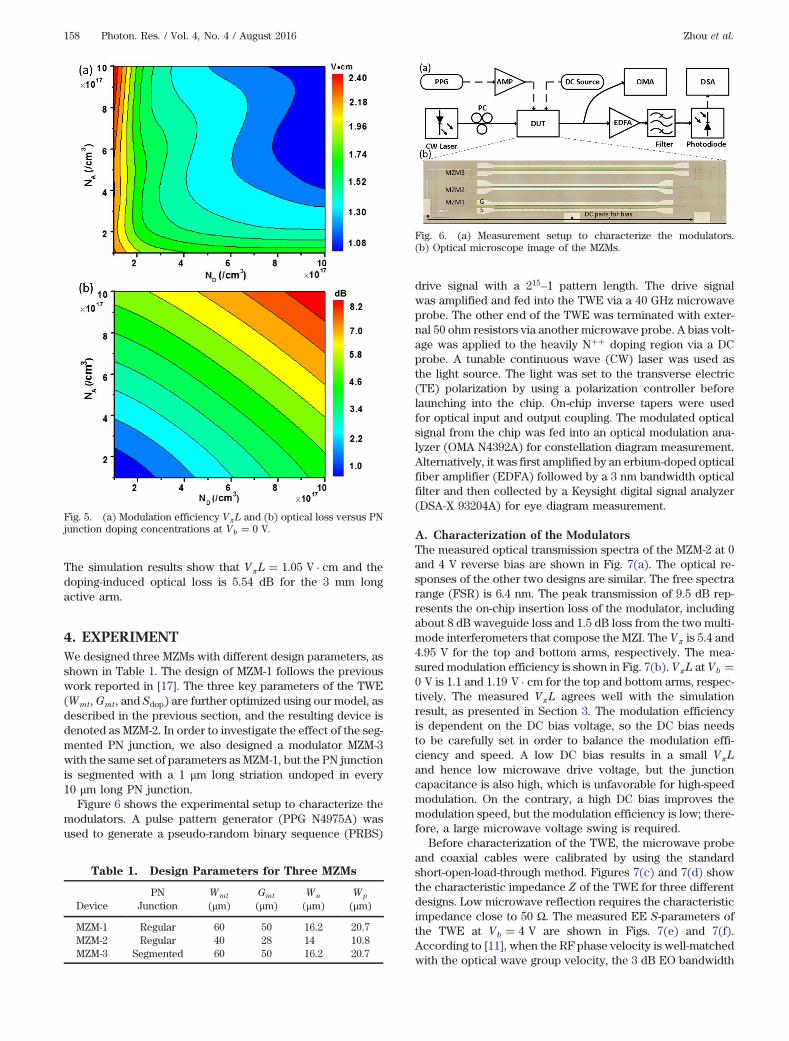
The simulation results show that VπL � 1.05 V · cm and thedoping-induced optical loss is 5.54 dB for the 3 mm longactive arm.
4. EXPERIMENTWe designed three MZMs with different design parameters, asshown in Table 1. The design of MZM-1 follows the previouswork reported in [17]. The three key parameters of the TWE(Wmt, Gmt, and Sdop) are further optimized using our model, asdescribed in the previous section, and the resulting device isdenoted as MZM-2. In order to investigate the effect of the seg-mented PN junction, we also designed a modulator MZM-3with the same set of parameters as MZM-1, but the PN junctionis segmented with a 1 μm long striation undoped in every10 μm long PN junction.
Figure 6 shows the experimental setup to characterize themodulators. A pulse pattern generator (PPG N4975A) wasused to generate a pseudo-random binary sequence (PRBS)
drive signal with a 215–1 pattern length. The drive signalwas amplified and fed into the TWE via a 40 GHz microwaveprobe. The other end of the TWE was terminated with exter-nal 50 ohm resistors via another microwave probe. A bias volt-age was applied to the heavily N�� doping region via a DCprobe. A tunable continuous wave (CW) laser was used asthe light source. The light was set to the transverse electric(TE) polarization by using a polarization controller beforelaunching into the chip. On-chip inverse tapers were usedfor optical input and output coupling. The modulated opticalsignal from the chip was fed into an optical modulation ana-lyzer (OMA N4392A) for constellation diagram measurement.Alternatively, it was first amplified by an erbium-doped opticalfiber amplifier (EDFA) followed by a 3 nm bandwidth opticalfilter and then collected by a Keysight digital signal analyzer(DSA-X 93204A) for eye diagram measurement.
A. Characterization of the ModulatorsThe measured optical transmission spectra of the MZM-2 at 0and 4 V reverse bias are shown in Fig. 7(a). The optical re-sponses of the other two designs are similar. The free spectrarange (FSR) is 6.4 nm. The peak transmission of 9.5 dB rep-resents the on-chip insertion loss of the modulator, includingabout 8 dB waveguide loss and 1.5 dB loss from the two multi-mode interferometers that compose the MZI. The V π is 5.4 and4.95 V for the top and bottom arms, respectively. The mea-sured modulation efficiency is shown in Fig. 7(b). VπL at Vb �0 V is 1.1 and 1.19 V · cm for the top and bottom arms, respec-tively. The measured VπL agrees well with the simulationresult, as presented in Section 3. The modulation efficiencyis dependent on the DC bias voltage, so the DC bias needsto be carefully set in order to balance the modulation effi-ciency and speed. A low DC bias results in a small VπL
and hence low microwave drive voltage, but the junctioncapacitance is also high, which is unfavorable for high-speedmodulation. On the contrary, a high DC bias improves themodulation speed, but the modulation efficiency is low; there-fore, a large microwave voltage swing is required.
Before characterization of the TWE, the microwave probeand coaxial cables were calibrated by using the standardshort-open-load-through method. Figures 7(c) and 7(d) showthe characteristic impedance Z of the TWE for three differentdesigns. Low microwave reflection requires the characteristicimpedance close to 50 Ω. The measured EE S-parameters ofthe TWE at Vb � 4 V are shown in Figs. 7(e) and 7(f).According to [11], when the RF phase velocity is well-matchedwith the optical wave group velocity, the 3 dB EO bandwidth
Fig. 5. (a) Modulation efficiency VπL and (b) optical loss versus PNjunction doping concentrations at Vb � 0 V.
Table 1. Design Parameters for Three MZMs
DevicePN
JunctionWmt
(μm)Gmt
(μm)Wn
(μm)Wp
(μm)
MZM-1 Regular 60 50 16.2 20.7MZM-2 Regular 40 28 14 10.8MZM-3 Segmented 60 50 16.2 20.7
Fig. 6. (a) Measurement setup to characterize the modulators.(b) Optical microscope image of the MZMs.
158 Photon. Res. / Vol. 4, No. 4 / August 2016 Zhou et al.

is given by the 6.4 dB EE bandwidth. The 6.4 dB EE bandwidthof all MZMs are above 25 GHz. Compared with MZM-1, MZM-3presents a higher EE bandwidth, indicating that the seg-mented PN junction can effectively reduce the microwaveloss. Return loss (S11) of the TWE indicates the microwavereflection at the entrance of the TWE due to impedance mis-match. The S11 of all MZMs are below −12 dB, suggesting verylow reflection from the 10 MHz to 32 GHz frequency range.Figure 7(g) shows the measured EO response of the modula-tor by using a lightwave component analyzer (LCA), whichcovers the frequency range from 100 MHz to 40 GHz. The elec-trical ports of the LCA were calibrated by the standard SLOTmethod. The EO 3 dB bandwidth of MZM-1 at Vb � 4 V is29 GHz. The MZM-2 has an improved EO bandwidth of33 GHz due to the optimization of the TWE. ComparingMZM-1 and MZM-3, we notice that the latter one with a seg-mented PN junction exhibits a slower roll-off, due to thelow microwave attenuation [see Fig. 4(d)]. To further improvethe modulator performance, the TWE in MZM-2 could also besegmented.
B. High-Speed OOK and BPSK ModulationsWe first performed the OOK modulation using the threemodulators. The RF drive signal was a 56 Gb/s PRBS signalamplified to a 7.8 V peak-to-peak voltage. A 6 V DC bias wassimultaneously applied to the MZM. The input laser wave-length was set at the quadrature point of the MZI. The mea-sured 56 Gb/s OOK modulation eye diagram of these MZMsare shown in the Figs. 8(a)–8(c). The top curves in each graphare the clock signal and the modulated optical waveforms. Itcan be seen that MZM-2 presents a better eye diagram thanthe other two. The measured ER is 4.0 dB, and the Q-factoris 3.73.
Fig. 7. (a) Optical transmission spectra of MZM-2 at 0 and 4 V reversebiases. (b) Modulation efficiency VπL of MZM-2. (c) Real partof the characteristic impedance. (d) Imaginary part of the character-istic impedance. (e) Microwave transmission response EE S21.(f) Microwave reflection response EE S11. (g) Modulator frequencyresponse EO S21.
Fig. 8. Measured 56 Gb/s OOK modulation eye diagrams for(a) MZM-1, (b) MZM-2, and (c) MZM-3.
Zhou et al. Vol. 4, No. 4 / August 2016 / Photon. Res. 159

We next carried out the BPSK modulation. The laser wave-length was tuned to the minimum transmission point, and theDC bias was set to Vb � 4 V. Figure 9 shows the eye diagramsof the 40 Gb/s BPSKmodulation. Themeasured BER of MZM-2is shown in Fig. 10(a). The inset shows the constellation dia-gram when the optical signal-to-noise-ratio is 15.56 dB. TheBPSK signal magnitude and phase errors are 18.9% and6.9°, respectively, and the error vector magnitude (EVM) isaround 22%. The Q-factor is 6.6. The BER deduced fromthe measured EVM is 1.96 × 10⁻¹⁵. The BER can be decreasedby increasing the received optical power. All the measuredBER are below the requirement in forward error correctiontechniques. The measured BER and constellation diagramof MZM-3 are shown in the Fig. 10(b). It has a similar modu-lation performance with MZM-2.
A low drive voltage is required in order for the modulatorsto be compatible with CMOS drive circuits. The drive voltagecan be lowered with an improved modulation efficiency eitherby increasing the doping concentration or designing a PNjunction that can provide more depletion overlap with thewaveguide mode. Interleaved PN junctions [4] or L-shaped/U-shaped PN junctions [28] could be used to ensure a lowV πL. In order to obtain a high EO bandwidth, the siliconsubstrate can even be etched off to give a better phase matchbetween the RF mode and the optical mode [29].
5. CONCLUSIONWe have established an equivalent circuit model for theCPS-TWE in a single-drive push–pull silicon modulator. The
partial-capacitance technique and conformal mapping wereused to calculate the capacitance contributed by each layer.Fringe capacitances were taken into consideration to accu-rately model the PN junction. The accuracy of the equivalentcircuit model was justified by comparing with numericalsimulations. Based on this model, we optimized the keyparameters in TWE design to achieve a large EO bandwidth.The segmented PN junction design was proved to be efficientin reducing the microwave loss. The doping concentrationswere chosen to make a compromise between modulation ef-ficiency and optical loss. The 3 dB EO bandwidth of the opti-mized 3 mm long MZM was measured to be 33 GHz at 4 Vreverse bias. 56 Gb/s OOK and 40 Gb/s BPSK modulationshave been successfully demonstrated.
Funding. National Natural Science Foundation ofChina (NSFC) (61422508, 61535006, 61661130155); ShanghaiRising-Star Program (14QA1402600).
Acknowledgment. We also thank IME Singapore fordevice fabrication.
REFERENCES1. G. T. Reed, G. Z. Mashanovich, F. Y. Gardes, and D. J. Thomson,
“Silicon optical modulators,” Nat. Photonics 4, 518–526 (2010).2. T. Y. Liow, K. W. Ang, Q. Fang, J. F. Song, Y. Z. Xiong, M. B. Yu,
G. Q. Lo, and D. L. Kwong, “Silicon modulators and germaniumphotodetectors on SOI: monolithic integration, compatibility,and performance optimization,” IEEE J. Sel. Top. QuantumElectron. 16, 307–315 (2010).
3. G. T. Reed, G. Z. Mashanovich, F. Y. Gardes, M. Nedeljkovic, Y.Hu, D. J. Thomson, K. Li, P. R. Wilson, S.-W. Chen, and S. S. Hsu,“Recent breakthroughs in carrier depletion based silicon opticalmodulators,” Nanophotonics 3, 229–245 (2014).
4. H. Xu, X. Y. Li, X. Xiao, Z. Y. Li, Y. D. Yu, and J. Z. Yu,“Demonstration and characterization of high-speed silicondepletion-mode Mach–Zehnder modulators,” IEEE J. Sel. Top.Quantum Electron. 20, 23–32 (2014).
5. D. J. Thomson, F. Y. Gardes, S. Liu, H. Porte, L. Zimmermann,J. M. Fedeli, Y. F. Hu, M. Nedeljkovic, X. Yang, P. Petropoulos,and G. Z. Mashanovich, “High performance Mach–Zehnder-based silicon optical modulators,” IEEE J. Sel. Top. QuantumElectron. 19, 85–94 (2013).
6. S. S. Azadeh, F. Merget, S. Romero-García, A. Moscoso-Mártir,N. von den Driesch, J. Müller, S. Mantl, D. Buca, and J. Witzens,“Low Vπ silicon photonics modulators with highly linear epitax-ially grown phase shifters,” Opt. Express 23, 23526–23550(2015).
7. X. Tu, T.-Y. Liow, J. Song, X. Luo, Q. Fang, M. Yu, and G.-Q. Lo,“50-Gb/s silicon optical modulator with traveling-wave elec-trodes,” Opt. Express 21, 12776–12782 (2013).
8. K. Goi, A. Oka, H. Kusaka, Y. Terada, K. Ogawa, T.-Y. Liow, X.Tu, G.-Q. Lo, and D.-L. Kwong, “Low-loss high-speed silicon IQmodulator for QPSK/DQPSK in C and L bands,”Opt. Express 22,10703–10709 (2014).
9. R. Ding, Y. Liu, Y. J. Ma, Y. S. Yang, Q. Li, A. E. J. Lim, G. Q. Lo, K.Bergman, T. Baehr-Jones, and M. Hochberg, “High-speed siliconmodulator with slow-wave electrodes and fully independent dif-ferential drive,” J. Lightwave Technol. 32, 2240–2247 (2014).
10. J. F. Ding, R. Q. Ji, L. Zhang, and L. Yang, “Electro-opticalresponse analysis of a 40 Gb/s silicon Mach-Zehnder opticalmodulator,” J. Lightwave Technol. 31, 2434–2440 (2013).
11. M. Streshinsky, R. Ding, Y. Liu, A. Novack, Y. Yang, Y. Ma, X. Tu,E. K. S. Chee, A. E.-J. Lim, and P. G.-Q. Lo, “Low power 50 Gb/ssilicon traveling wave Mach–Zehnder modulator near 1300 nm,”Opt. Express 21, 30350–30357 (2013).
12. D. Thomson, F. Gardes, Y. Hu, G. Mashanovich, M. Fournier, P.Grosse, J. Fedeli, and G. Reed, “High contrast 40 Gbit/s opticalmodulation in silicon,” Opt. Express 19, 11507–11516 (2011).
Fig. 9. 40 Gb/s BPSK modulation eye diagrams for (a) MZM-1,(b) MZM-2, and (c) MZM-3.
Fig. 10. Measured 40 Gb/s BPSK modulation BER curves for(a) MZM-2 and (b) MZM-3. Inset shows the constellation diagram.
160 Photon. Res. / Vol. 4, No. 4 / August 2016 Zhou et al.

13. J. Wang, C. Qiu, H. Li, W. Ling, L. Li, A. Pang, Z. Sheng, A. M. Wu,X. Wang, S. C. Zou, and F. W. Gan, “Optimization and demon-stration of a large-bandwidth carrier-depletion silicon opticalmodulator,” J. Lightwave Technol. 31, 4119–4125 (2013).
14. H. Yu and W. Bogaerts, “An equivalent circuit model of the trav-eling wave electrode for carrier-depletion-based silicon opticalmodulators,” J. Lightwave Technol. 30, 1602–1609 (2012).
15. H. Jayatilleka, W. D. Sacher, and J. K. S. Poon, “Analytical modeland fringing-field parasitics of carrier-depletion silicon-on-insulator optical modulation diodes,” IEEE Photon. J. 5,2200211 (2013).
16. P. Dong, L. Chen, and Y.-k. Chen, “High-speed low-voltagesingle-drive push-pull silicon Mach-Zehnder modulators,” Opt.Express 20, 6163–6169 (2012).
17. J. T. Wang, L. J. Zhou, H. K. Zhu, R. Yang, Y. Y. Zhou, L. Liu, T.Wang, and J. P. Chen, “Silicon high-speed binary phase-shift key-ing modulator with a single-drive push-pull high-speed travelingwave electrode,” Photon. Res. 3, 58–62 (2015).
18. H. K. Zhu, L. J. Zhou, T. Wang, L. Liu, C. Y. Wong, Y. Y. Zhou, R.Yang, X. W. Li, and J. P. Chen, “Optimized silicon QPSK modu-lator with 64-Gb/s modulation speed,” IEEE Photon. J. 7, 1–6(2015).
19. M. Chagnon, M. Morsy-Osman, M. Poulin, C. Paquet, S. Lessard,and D. V. Plant, “Experimental parametric study of a silicon pho-tonic modulator enabled 112-Gb/s PAM transmission systemwith a DAC and ADC,” J. Lightwave Technol. 33, 1380–1387(2015).
20. L. Chen, P. Dong, and Y. K. Chen, “Chirp and dispersion toler-ance of a single-drive push-pull silicon modulator at 28 Gb/s,”IEEE Photon. Technol. Lett. 24, 936–938 (2012).
21. Y. Zhou, L. Zhou, F. Su, J. Xie, H. Zhu, X. Li, and J. Chen,“Linearity measurement of a silicon single-drive push-pullMach-Zehnder modulator,” in Conference on Lasers andElectro-Optics (CLEO): Science and Innovations (OpticalSociety of America, 2015), paper SW3N-6.
22. E. L. Chen and S. Y. Chou, “Characteristics of coplanar trans-mission lines on multilayer substrates: modeling and experi-ments,” IEEE Trans. Microwave Theory Tech. 45, 939–945(1997).
23. V. Milanovic, M. Ozgur, D. C. DeGroot, J. A. Jargon, M. Gaitan,and M. E. Zaghloul, “Characterization of broad-band transmis-sion for coplanar waveguides on CMOS silicon substrates,”IEEE Trans. Microwave Theory Tech. 46, 632–640 (1998).
24. Y. R. Kwon, V. M. Hietala, and K. S. Champlin, “Quasi-TEManalysis of ‘slow-wave’ mode propagation on coplanar micro-structure MIS transmission lines,” IEEE Trans. MicrowaveTheory Tech. 35, 545–551 (1987).
25. T. Baehr-Jones, R. Ding, Y. Liu, A. Ayazi, T. Pinguet, N. C. Harris,M. Streshinsky, P. Lee, Y. Zhang, and A. E.-J. Lim, “Ultralowdrive voltage silicon traveling-wave modulator,” Opt. Express20, 12014–12020 (2012).
26. W. Heinrich, “Quasi-TEM description of MMIC coplanar lines in-cluding conductor-loss effects,” IEEE Trans. Microwave TheoryTech. 41, 45–52 (1993).
27. D. Petousi, L. Zimmermann, A. Gajda, M. Kroh, K. Voigt, G.Winzer, B. Tillack, and K. Petermann, “Analysis of optical andelectrical tradeoffs of traveling-wave depletion-type Si Mach–Zehnder modulators for high-speed operation,” IEEE J. Sel.Top. Quantum Electron. 21, 199–206 (2015).
28. K. Goi, N. Ishikura, H. Ishihara, S. Sakamoto, K. Ogawa,T.-Y. Liow, X. Tu, G.-Q. Lo, and D. L. Kwong, “Low-voltagesilicon Mach-Zehnder modulator operating at high tempera-tures without thermo-electric cooling,” in Optical FiberCommunication Conference (Optical Society of America,2016), paper W2A–23.
29. X. Xiao, M. Li, Z. Li, L. Wang, Q. Yang, and S. Yu, “Substrateremoved silicon Mach-Zehnder modulator for high baudrate optical intensity modulations,” in Optical FiberCommunication Conference (Optical Society of America,2016), paper Th4H-5.
Zhou et al. Vol. 4, No. 4 / August 2016 / Photon. Res. 161