Embed Size (px)
Citation preview
Modeling, Analysis and Control of DC Hybrid
Power Systems
by
Yanhui Xie
A dissertation submitted in partial fulfillment
of the requirements for the degree of
Doctor of Philosophy
(Naval Architecture and Marine Engineering)
in The University of Michigan
2010
Doctoral Committee:
Professor Jing Sun, Co-Chair
Professor James S. Freudenberg, Co-Chair
Associate Professor Chunting Mi
Assistant Professor Ryan Eustice

c© Yanhui Xie 2010
All Rights Reserved

Dedicated to my daughter, Xiwen Xie, and to my wife, Yunyun Ni.
ii

Acknowledgements
Many people have contributed to the production of this dissertation, although
only my name appears on the cover. Hence, I absolutely owe my gratitude to all
those people who encouraged and helped me to finally finish this dissertation.
My deepest gratitude is to my advisors, Professor Jing Sun and Professor James
S. Freudenberg, at the University of Michigan. Their consistent encouragement and
support helped me overcome many challenges and finish this dissertation. I am ex-
tremely thankful to Professor Chunting Mi. I spent almost one year in his power
electronics lab to build our hybrid power system testbed which has significantly con-
tributed to this dissertation. I am also thankful to Professor Ryan Eustice for his
constructive comments and suggestions.
I would like to gratefully and sincerely thank all my friends and colleagues in
the RACE Lab at the University of Michigan for valuable discussions and enjoyable
friendship. Specifically, I would like to thank Reza Ghaemi, Handa Xi, Zhen Li,
Gayathri Seenumani, Christopher Vermillion, Vasilios Tsourapas, Soryeok Oh, Amey
Karnik, Jian Chen, and Zhao Lu.
I also like to acknowledge the U.S. Office of Naval Research for the financial
support under Grants No. N00014-08-1-0611 and N00014-05-1-0533.
Finally, and most importantly, I would like to thank my wife Yunyun Ni. Without
her support, encouragement, patience and unwavering love, I may never have finished
iii

this dissertation. I thank my parents, Shiqi Xie and Xiangyun Meng, and Yunyun’s
parents, Guofu Ni and Huiying Zhang, who always have their faith in me and give
me the support and strength to overcome the difficulties.
iv

Contents
Dedication . . . . . . . . . . . . . . . . . . . . . . . . . . . . . . . . . . . . . ii
Acknowledgements . . . . . . . . . . . . . . . . . . . . . . . . . . . . . . . iii
List of Figures . . . . . . . . . . . . . . . . . . . . . . . . . . . . . . . . . . viii
List of Tables . . . . . . . . . . . . . . . . . . . . . . . . . . . . . . . . . . . xii
List of Abbreviations . . . . . . . . . . . . . . . . . . . . . . . . . . . . . . xiii
Abstract . . . . . . . . . . . . . . . . . . . . . . . . . . . . . . . . . . . . . . xv
Chapters
1 Introduction . . . . . . . . . . . . . . . . . . . . . . . . . . . . . . . 1
1.1 Background and Literature Review . . . . . . . . . . . . . . . 2
1.1.1 Integrated Power System of All Electric Ships . . . . 2
1.1.2 DC Hybrid Power System . . . . . . . . . . . . . . . . 4
1.1.3 Full Bridge and Dual Active Bridge Converters . . . . 5
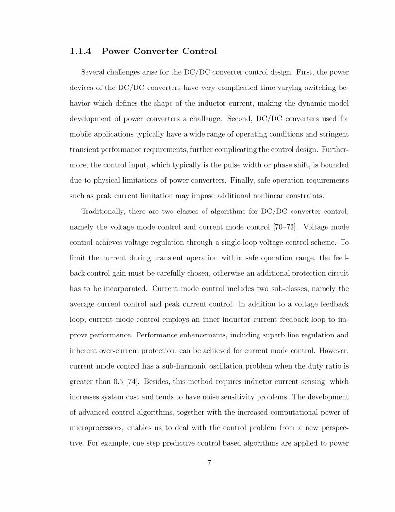
1.1.4 Power Converter Control . . . . . . . . . . . . . . . . 7
1.2 Dissertation Scope and Contributions . . . . . . . . . . . . . 9
1.2.1 Dissertation Scope . . . . . . . . . . . . . . . . . . . . 9
1.2.2 Contributions . . . . . . . . . . . . . . . . . . . . . . 12
1.3 Dissertation Overview . . . . . . . . . . . . . . . . . . . . . . 14
v
2 DC Hybrid Power System Testbed Development . . . . . . . . . . . 17
2.1 DHPS Testbed Development . . . . . . . . . . . . . . . . . . 18
2.2 Summary . . . . . . . . . . . . . . . . . . . . . . . . . . . . . 23
3 Modeling and Simulation of an Integrated Power System for an All
Electric Ship . . . . . . . . . . . . . . . . . . . . . . . . . . . . . . . 24
3.1 Modeling of IPS . . . . . . . . . . . . . . . . . . . . . . . . . 24
3.1.1 Gas Turbine Module . . . . . . . . . . . . . . . . . . . 25
3.1.2 Fuel Cell and Reforming Unit Module . . . . . . . . . 29
3.1.3 ZEDS Module . . . . . . . . . . . . . . . . . . . . . . 33
3.1.4 Propulsion Module . . . . . . . . . . . . . . . . . . . 36
3.2 Model Integration, Distribution and Preliminary Simulation . 37
3.2.1 Model Integration and Distribution . . . . . . . . . . 37
3.2.2 Preliminary Simulations . . . . . . . . . . . . . . . . . 39
3.3 Graphical User Interface (GUI) Development . . . . . . . . . 41
3.4 Summary . . . . . . . . . . . . . . . . . . . . . . . . . . . . . 43
4 Power Flow Characterization of the Dual Active Bridge Converter . 45
4.1 Fundamental Phenomena of DABCs . . . . . . . . . . . . . . 45
4.2 Conventional Power Flow Analysis . . . . . . . . . . . . . . . 51
4.3 Effects of Minor Parameters on Power Transfer of the DABC 54
4.3.1 Power Semiconductor Voltage Loss Effect . . . . . . . 55
4.3.2 Dead Time Effect . . . . . . . . . . . . . . . . . . . . 57
4.4 Power Flow Characterization of the DABC over a Wide Op-
erating Range . . . . . . . . . . . . . . . . . . . . . . . . . . 64
4.5 Experimental Validation . . . . . . . . . . . . . . . . . . . . 73
4.6 Summary . . . . . . . . . . . . . . . . . . . . . . . . . . . . . 76
5 Development of a Current-Mode PWM Strategy for the Dual Active
Bridge Converter . . . . . . . . . . . . . . . . . . . . . . . . . . . . . 77
5.1 CM-PWM Strategy . . . . . . . . . . . . . . . . . . . . . . . 77
vi
5.2 Power Converter Characteristics of DABC with CM-PWM . 81
5.2.1 Power Flow Calculation . . . . . . . . . . . . . . . . . 82
5.2.2 Current Stress . . . . . . . . . . . . . . . . . . . . . . 83
5.2.3 Soft-Switching Range . . . . . . . . . . . . . . . . . . 84
5.3 Experimental Validation . . . . . . . . . . . . . . . . . . . . 85
5.4 Summary . . . . . . . . . . . . . . . . . . . . . . . . . . . . . 87
6 Experimental Validation of the DHPS . . . . . . . . . . . . . . . . . 89
6.1 Power Converter Controller Development . . . . . . . . . . . 90
6.2 Experimental Results . . . . . . . . . . . . . . . . . . . . . . 96
6.3 Summary . . . . . . . . . . . . . . . . . . . . . . . . . . . . . 98
7 Model Predictive Control of the Full Bridge Converter . . . . . . . . 100
7.1 Inductor Peak Current Constraint . . . . . . . . . . . . . . . 101
7.2 Nonlinear Dynamic Model and Observer . . . . . . . . . . . . 106
7.3 MPC Formulation . . . . . . . . . . . . . . . . . . . . . . . . 107
7.3.1 Offset-Free Linear MPC Formulation . . . . . . . . . 108
7.3.2 Nonlinear MPC Formulation . . . . . . . . . . . . . . 111
7.4 InPA-SQP Algorithm . . . . . . . . . . . . . . . . . . . . . . 114
7.5 Experimental Validation . . . . . . . . . . . . . . . . . . . . 121
7.6 Summary . . . . . . . . . . . . . . . . . . . . . . . . . . . . . 125
8 Conclusions and Future Work . . . . . . . . . . . . . . . . . . . . . . 127
8.1 Conclusions . . . . . . . . . . . . . . . . . . . . . . . . . . . 127
8.2 Future Work . . . . . . . . . . . . . . . . . . . . . . . . . . . 130
Appendix . . . . . . . . . . . . . . . . . . . . . . . . . . . . . . . . . . . . . 132
Bibliography . . . . . . . . . . . . . . . . . . . . . . . . . . . . . . . . . . . 136
vii
List of Figures
Figure
1.1 One-line diagram for integrated power system of all electric ship. . . . 3
1.2 Configuration of a DHPS. . . . . . . . . . . . . . . . . . . . . . . . . 11
2.1 DC hybrid power system testbed setup. . . . . . . . . . . . . . . . . . 18
2.2 Configuration of the power stage of a DHPS with energy storage bank. 19
2.3 RT-Lab real-time simulation system configuration. . . . . . . . . . . . 21
2.4 Bidirectional DC/DC converter. . . . . . . . . . . . . . . . . . . . . . 22
3.1 Schematic of the gas turbine/generator system. . . . . . . . . . . . . 25
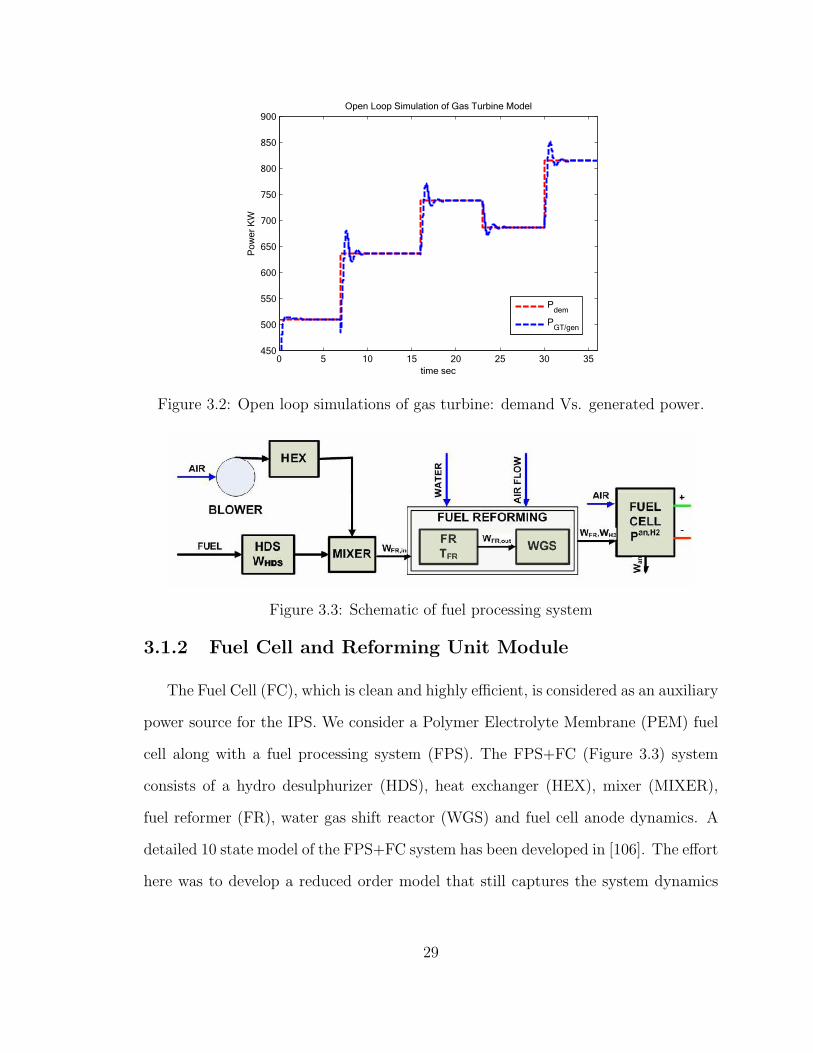
3.2 Open loop simulations of gas turbine: demand Vs. generated power. 29
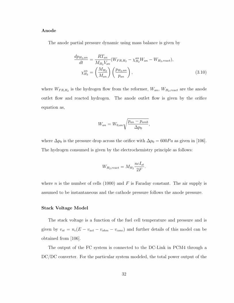
3.3 Schematic of fuel processing system . . . . . . . . . . . . . . . . . . . 29
3.4 Open loop simulations of fuel cell: current demand and generated
power. . . . . . . . . . . . . . . . . . . . . . . . . . . . . . . . . . . 33
3.5 SimPowerSystems/ARTEMIS model of PCM1 in ZEDS. . . . . . . . 34
3.6 Diagram of PCMs in ZEDS. . . . . . . . . . . . . . . . . . . . . . . . 35
3.7 Power consumed by loads at failure and reconfiguration scenarios. . . 40
3.8 Propulsion motor transient. . . . . . . . . . . . . . . . . . . . . . . . 41
3.9 The top level GUI of the IPS. . . . . . . . . . . . . . . . . . . . . . . 42
3.10 Failure, reconfiguration, operation and drive scenarios GUI. . . . . . . 43
4.1 Dual active bridge DC/DC converter topology. . . . . . . . . . . . . . 46
viii

4.2 Phase shift modulation of DAB converter: (a) modulation sequence;
(b) ideal voltage and current waveforms. . . . . . . . . . . . . . . . . 47
4.3 Simplified scheme of a dual active bridge DC/DC converter . . . . . . 47
4.4 Internal power transfer for phase shift β3 = 0. . . . . . . . . . . . . . 48
4.5 Power flow curves for Vo = 80V . . . . . . . . . . . . . . . . . . . . . . 49
4.6 Measured efficiency curve for Vsc = 30. . . . . . . . . . . . . . . . . . 50
4.7 Phase drift phenomenon for Vsc = 30 and phase shift= 0 (The two
plots at the bottom are zoomed in characteristics of the top one.). . . 51
4.8 Ideal waveforms of DAB converter considering power semiconductor
voltage loss. . . . . . . . . . . . . . . . . . . . . . . . . . . . . . . . . 55
4.9 Dead time effect of DAB converter. . . . . . . . . . . . . . . . . . . . 59
4.10 Power flow model validation for Vo = 80V and β3 = 0: (a) P5; (b) P6. 63
4.11 Operating region separation. . . . . . . . . . . . . . . . . . . . . . . . 65
4.12 Ideal waveforms for DAB converter with phase shift modulation strategy. 68
4.13 Power flow characteristics for Vsc = 30V , Vo = 80V , Vs = 2V , Vd = 1V
and Td = 2.5µs. . . . . . . . . . . . . . . . . . . . . . . . . . . . . . . 71
4.14 The minor parameters impact on power flow characteristics for Vsc =
30V and β3 ∈ [0, 0.26]. . . . . . . . . . . . . . . . . . . . . . . . . . . 72
4.15 Power flow curve for Vsc = 30V . . . . . . . . . . . . . . . . . . . . . . 73
4.16 Power flow curve for Vsc = 40V . . . . . . . . . . . . . . . . . . . . . . 74
4.17 Power flow curve for Vsc = 50V . . . . . . . . . . . . . . . . . . . . . . 75
5.1 CM-PWM of the DAB converter (a) modulation sequence; (b) ideal
waveforms. . . . . . . . . . . . . . . . . . . . . . . . . . . . . . . . . . 79
5.2 Experimental waveforms for Vsc = 40, Vo = 100 and β3 = 0.8. . . . . . 86
5.3 Power flow curves for Vo = 100. . . . . . . . . . . . . . . . . . . . . . 86
5.4 The efficiency curves of the DAB converter: (a) with PSM; (b) with
CM-PWM. . . . . . . . . . . . . . . . . . . . . . . . . . . . . . . . . 87
6.1 Configuration of the DHPS control scheme. . . . . . . . . . . . . . . . 90
ix
6.2 Configuration of the power management control scheme for a FBC. . 91
6.3 Open-loop Bode plot of the FBC at different values of output power. 92
6.4 Closed-loop Bode plot of the FBC at different values of output power. 93
6.5 Open-loop Bode plot of the DABC at different values of input voltage
and output power. . . . . . . . . . . . . . . . . . . . . . . . . . . . . 95
6.6 Closed-loop Bode plot of the DABC at different values of input voltage
and output power. . . . . . . . . . . . . . . . . . . . . . . . . . . . . 95
6.7 Experimental results of constant power charging mode. . . . . . . . . 97
6.8 Experimental results of step-change power charging mode. . . . . . . 97
6.9 Experimental results of step-change power discharging mode. . . . . . 98
7.1 A full bridge DC/DC converter. . . . . . . . . . . . . . . . . . . . . . 101
7.2 Modulation sequence and ideal waveforms of the full bridge DC/DC
converter for DCM. . . . . . . . . . . . . . . . . . . . . . . . . . . . . 102
7.3 Modulation sequence and ideal waveforms of the full bridge DC/DC
converter for CCM. . . . . . . . . . . . . . . . . . . . . . . . . . . . . 103
7.4 Simplified scheme of a full bridge DC/DC converter. . . . . . . . . . . 104
7.5 DCM/CCM boundary line Lβ1b and peak current constraint curves
Lβ1d and Lβ1c for V1 = 60V and ipk = 75A. . . . . . . . . . . . . . . . 105
7.6 Intermediate initial conditions which handle the large perturbation. . 115
7.7 Flowchart of the InPA-SQP algorithm. . . . . . . . . . . . . . . . . . 120
7.8 Performance comparison of LMPC with different prediction horizon for
a step-down change of R from 12.8Ω to 6.4Ω. . . . . . . . . . . . . . . 121
7.9 Performance comparison of NLMPC with different prediction horizon
for a step-down change of R from 12.8Ω to 6.4Ω. . . . . . . . . . . . . 122
7.10 Comparison of the LMPC and NLMPC schemes during the starting
process. . . . . . . . . . . . . . . . . . . . . . . . . . . . . . . . . . . 123
7.11 Comparison of the LMPC and NLMPC schemes for a step-down change
of R from 12.8Ω to 6.4Ω. . . . . . . . . . . . . . . . . . . . . . . . . . 124
x

7.12 Comparison of the LMPC and NLMPC schemes under overload oper-
ation condition. . . . . . . . . . . . . . . . . . . . . . . . . . . . . . . 125
xi

List of Tables
Table
2.1 Parameters of the testbed prototype . . . . . . . . . . . . . . . . . . 19
3.1 GT Modeling Nomenclature . . . . . . . . . . . . . . . . . . . . . . . 27
3.2 FC Modeling Nomenclature . . . . . . . . . . . . . . . . . . . . . . . 31
4.1 Voltage across the leakage inductor considering power semiconductors
voltage loss . . . . . . . . . . . . . . . . . . . . . . . . . . . . . . . . 56
4.2 Voltage across the leakage inductor for case I . . . . . . . . . . . . . . 60
4.3 Voltage across the leakage inductor for case II . . . . . . . . . . . . . 61
4.4 Power flow characterization table . . . . . . . . . . . . . . . . . . . . 69
6.1 Feedback control gains of the power converters . . . . . . . . . . . . . 96
7.1 Performance summarization of the LMPC . . . . . . . . . . . . . . . 122
7.2 Performance summarization of the NLMPC . . . . . . . . . . . . . . 123
xii
List of Abbreviations
AES All Electric Ship
CM-PWM Current Mode Pulse Width Modulation
DABC Dual Active Bridge Converter
DHPS DC Hybrid Power System
EPM Electric Propulsion Module
FBC Full Bridge Converter
FPS Fuel Processing System
FR Fuel Reformer
HDS Hydro Desulphurizer
HEX Heat Exchanger
MIXER Mixer
InPA-SQP Integrated Perturbation Analysis and
Sequential Quadratic Programming
IPS Integrated Power System
LMPC Linear Model Predictive Control
MPC Model Predictive Control
NLMPC Nonlinear Model Predictive Control
xiii

PCM Power Conversion Module
PEM Polymer Electrolyte Membrane
PGM Power Generation Module
PMSM Permanent Magnet Synchronous Motor
PSM Phase Shift Modulation
PWM Pulse Width Modulation
WGS Water Gas Shift reactor
UPS Uninterruptible Power Supply
xiv
Abstract
Modeling, Analysis and Control of DC Hybrid Power Systems
by
Yanhui Xie
Co-Chairs: Jing Sun and James S. Freudenberg
All electric ships are featured with integrated power systems which combine elec-
tric propulsion technology with heterogeneous power generation and distribution tech-
nologies to form one single electrical platform. The auxiliary and main power gener-
ation system form an isolated hybrid power system to feed the ship service loads and
to meet the propulsion power requirement. Although for decades, the methodologies
for power converter control have been explored in many publications, the modeling,
analysis, and control of hybrid power systems with multiple power converters remains
an interesting open problem, leading to its exclusive focus in this dissertation.
Along with the opportunities introduced by hybrid power systems, the inter-
connectivity and complexity represent a major system analysis, design and optimiza-
tion challenge, calling for the development of effective tools. Therefore, a compre-
hensive testbed is developed. Moreover, component level modeling, analysis and
modulation strategy development are performed to ensure system level performance.
A new power flow model for the dual active bridge converter is derived. The new
model provides a physical interpretation of the observed phenomena and identifies
xv

other characteristics that are validated by experiments. To overcome the drawbacks
of traditional modulation strategies, a novel modulation strategy is developed for the
dual active bridge converter. The experimental results verified that, if the new strat-
egy is used to modulate the dual active bridge converter, this testbed can be used as
an effective tool for optimal power management algorithm development for the hybrid
power systems.
The development of advanced control algorithms, together with the increased
computational power of microprocessors, enables us to deal with the control problem
from a new perspective. In this dissertation, the voltage regulation problem for a full
bridge DC/DC converter is formulated as both a linear and a nonlinear Model Pre-
dictive Control (MPC) problem with a nonlinear constraint that captures the peak
current protection requirement. The experimental results reveal that both the MPC
algorithms can successfully achieve voltage regulation and peak current protection.
The successful implementation of the MPC schemes on the full bridge DC/DC con-
verter paves the way for future system-level advanced control algorithm development
for hybrid power systems.
xvi

Chapter 1
Introduction
Next generation All Electric Ships (AES) is enabled by Integrated Power Systems
(IPS) which incorporate a set of primary and auxiliary power sources to provide the
propulsion power and, at the same time, energize the shipboard electric loads [1, 2].
The IPS is mainly comprised of Power Generation Modules (PGM), Power Conversion
Modules (PCM), Electric Propulsion Modules (EPM) and vital/nonvital loads. The
PGM could be a gas turbine, diesel engine or fuel cell power system. The auxiliary
power generation system, such as a fuel cell power system, usually only energizes the
ship service loads while the main power generation systems, such as the gas turbine
and diesel engine, provide power for both the propulsion loads and the ship service
loads. Therefore, the auxiliary and main power generation system form an isolated
hybrid power system to feed the ship service loads and to meet the propulsion power
requirements.
As the power conditioning device, the power converter is the enabling technology
to address the power management problems for the hybrid power system. However,
for the isolated hybrid power system of the IPS, the wide range of operating condi-
tions, the requirements for fast power response and load following, coupled with the
1

stringent constraints of high power quality and system reliability, have imposed chal-
lenges for control of the power converters whose dynamic characteristics are highly
nonlinear. Motivated by the challenges and importance of the hybrid power system
controls, this dissertation has focused on modeling, analysis and control of power
converters for the hybrid power systems.
1.1 Background and Literature Review
1.1.1 Integrated Power System of All Electric Ships
An Integrated Power System (IPS) of an AES provides electric power to all ship-
board loads, including the propulsion system, with an integrated plant [1, 2]. The
IPS associated with the AES typically has electric propulsion, sophisticated electric
weaponry systems and ship service as electric loads. Unlike a traditional mechanical
propulsion system which uses long shafts to deliver energy from the prime movers to
the propulsion systems, the electric propulsion systems, including motor drives and
electric motors, are connected to the power plants through an electrical distribution
system. Under emergent battle scenarios, a large amount of power can be unlocked
from the propulsion system to support the electric weaponry systems. Moreover, ship
service loads are powered from the same power network as the electric propulsion
system through a power distribution system.
To enhance the reliability and survivability of the IPS, Zonal Electric Distribution
System (ZEDS) was introduced [3,4]. Unlike the conventional radial electric distribu-
tion system which radially distributes power to the loads through load centers, ZEDS
employs two main buses (starboard bus and port bus) to provide redundant power
flow paths for vital loads. With the introduction of Power Electronic Building Block
(PEBB) [5,6], the ZEDS could seamlessly and dynamically reconfigure the power flow
2
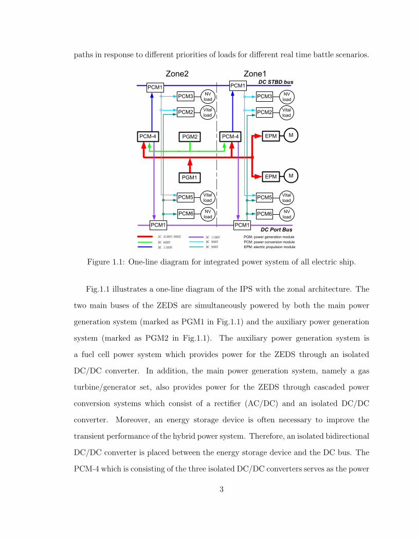
paths in response to different priorities of loads for different real time battle scenarios.
DC STBD bus
DC Port Bus
PCM1NV loadPCM3
Vital loadPCM2
NV loadPCM6
Vital loadPCM5
MEPM
MEPM
PCM1
PCM1
NV loadPCM3
Vital loadPCM2
NV loadPCM6
Vital loadPCM5
PGM2PCM-4
PCM1
PCM-4
AC 4160V/60HZ
DC 600V
DC 1100V
DC 900V
DC 900V
PGM: power generation modulePCM: power conversion moduleEPM: electric propulsion module
PGM1
DC 1100V
Figure 1.1: One-line diagram for integrated power system of all electric ship.
Fig.1.1 illustrates a one-line diagram of the IPS with the zonal architecture. The
two main buses of the ZEDS are simultaneously powered by both the main power
generation system (marked as PGM1 in Fig.1.1) and the auxiliary power generation
system (marked as PGM2 in Fig.1.1). The auxiliary power generation system is
a fuel cell power system which provides power for the ZEDS through an isolated
DC/DC converter. In addition, the main power generation system, namely a gas
turbine/generator set, also provides power for the ZEDS through cascaded power
conversion systems which consist of a rectifier (AC/DC) and an isolated DC/DC
converter. Moreover, an energy storage device is often necessary to improve the
transient performance of the hybrid power system. Therefore, an isolated bidirectional
DC/DC converter is placed between the energy storage device and the DC bus. The
PCM-4 which is consisting of the three isolated DC/DC converters serves as the power
3

conditioning system for the main power generation system, auxiliary power generation
system and energy storage system. The output terminals of the three converters are
connected together to feed DC buses of the ZEDS, therefore forming a DC Hybrid
Power System (DHPS) for the IPS of an AES [92,93].
1.1.2 DC Hybrid Power System
Hybridization through integration of multiple power sources, especially those with
complementary characteristics, can achieve high system performance and reliability.
For example, wind energy, if combined with micro-hydro or diesel power generation
[20], [21], can provide low cost and high reliability power solutions for island and
remote area communities. The integration of fuel cells to shipboard power systems
[22, 93] and to automotive powertrains [23, 27–29] results in low emissions and high
system efficiency.
Since these power sources have different response time and efficiency, dynamic
optimal power management is critical to the power system stability, efficiency and
performance [67–69]. Therefore, how to coordinate the power converters to achieve
optimal efficiency and maximum reliability during transients is a big challenge for the
power management system of the DHPS.
Even though power converters have been widely used in industry, commercial, and
military applications, their utility in multi-source, multi-load hybrid power systems
has brought many new challenges in their design, integration and control. For exam-
ple, they typically require a wide operating range and fast transient response, thereby
placing new emphasis on dynamic response. The need to have multiple converters
work in concert also demands coordinated control to manage the dynamic interac-
tions among involved components. On one hand, stringent safety and reliability
requirements mandate a total protection of the system from constraint violation and
4

component failure. On the other hand, demands for high efficiency and fast transient
response render the conservative safety oriented strategy insufficient. Therefore, how
to achieve high system efficiency and superior transient performance without com-
promising system integrity becomes one of the focuses in power converter design and
optimal control.
1.1.3 Full Bridge and Dual Active Bridge Converters
Since a DHPS usually has multiple energy storage device and power sources,
there must be multiple power converters to serve as the power conditioning devices.
The full bridge and dual active bridge topologies were initially proposed in previous
studies [54], [55] for both high power density and high power applications. They are
very attractive because of their zero voltage switching, low component stresses, and
high power density features. Moreover, the high frequency transformer prevents fault
propagation and enables a flexible output/input voltage ratio. Therefore, with a full
bridge or a dual active bridge DC/DC converter as the power conditioning system,
different types of power sources and energy storage systems can be applied to high
DC voltage applications, such as the DC zonal electrical distribution system of an all
electric ship [93].
The Dual Active Bridge Converter (DABC) has been widely used in applications
such as Uninterruptible Power Supplies (UPS), battery charging and discharging sys-
tems, and auxiliary power supplies for hybrid electrical vehicles. For example, in [34],
the authors investigated an off-line UPS design based on dual active bridge topology.
The use of a DABC for bidirectional energy delivery between an energy storage system
and a DC power system is addressed in [35–38]. In [39, 43–45], the authors evaluate
different dual active bridge configurations for automotive applications. [46–48] adopt
a DABC as the core circuit of the power conversion system between an AC power
5

system and a DC voltage source.
For applications which involve energy storage systems, DABCs are expected to
operate over a wide range of operating conditions without substantial performance
degradation, especially for mobile applications. However, several issues have been
reported in the literature when the magnitude of the input and output voltage does
not match. First, the soft-switching region, in which switching losses can be min-
imized, will be significantly reduced [38, 54, 55], which leads to high switching loss.
Second, the circulating energy will be substantial [32, 49–51, 54, 55], which leads to
high conduction loss. Therefore, high power loss and low system efficiency for certain
operating conditions will be expected if the DABC operates with a wide input volt-
age range. Moreover, our experiments revealed several additional phenomena such as
the internal power transfer and phase drift, that deteriorate the performance of the
DABC [94,95].
To eliminate the circulating energy and extend the soft-switching range, several
modulation strategies are proposed and evaluated [32, 35, 36, 53]. Those strategies
introduce multiple control inputs to adjust the pulse width of the AC voltage of the
two full bridges and their phase difference respectively, leading to an over-actuated
system with complicated characteristics. To improve the system efficiency, resonant
converters have been studied extensively in [11–13, 17–19, 24–26, 30, 31, 40–42, 63].
To extend the power range of the DAB converter for ultra-capacitor applications,
a triangular modulation strategy is proposed [52] for low power applications. For
high power applications, the triangular shape of the inductor current leads to a high
RMS value and high peak current, causing low system efficiency and high component
current stress [52].
6
1.1.4 Power Converter Control
Several challenges arise for the DC/DC converter control design. First, the power
devices of the DC/DC converters have very complicated time varying switching be-
havior which defines the shape of the inductor current, making the dynamic model
development of power converters a challenge. Second, DC/DC converters used for
mobile applications typically have a wide range of operating conditions and stringent
transient performance requirements, further complicating the control design. Further-
more, the control input, which typically is the pulse width or phase shift, is bounded
due to physical limitations of power converters. Finally, safe operation requirements
such as peak current limitation may impose additional nonlinear constraints.
Traditionally, there are two classes of algorithms for DC/DC converter control,
namely the voltage mode control and current mode control [70–73]. Voltage mode
control achieves voltage regulation through a single-loop voltage control scheme. To
limit the current during transient operation within safe operation range, the feed-
back control gain must be carefully chosen, otherwise an additional protection circuit
has to be incorporated. Current mode control includes two sub-classes, namely the
average current control and peak current control. In addition to a voltage feedback
loop, current mode control employs an inner inductor current feedback loop to im-
prove performance. Performance enhancements, including superb line regulation and
inherent over-current protection, can be achieved for current mode control. However,
current mode control has a sub-harmonic oscillation problem when the duty ratio is
greater than 0.5 [74]. Besides, this method requires inductor current sensing, which
increases system cost and tends to have noise sensitivity problems. The development
of advanced control algorithms, together with the increased computational power of
microprocessors, enables us to deal with the control problem from a new perspec-
tive. For example, one step predictive control based algorithms are applied to power
7
electronics system, see e.g., [75] while Model Predictive Control (MPC) has been im-
plemented in an electric drive system for direct torque control [76,77] and in a flying
capacitor converter [78]. For the full bridge DC/DC converter under investigation,
the peak current protection problem can be formulated as a constraint for an optimal
control problem, which can be effectively dealt with using MPC.
MPC, also known as receding horizon control, is a class of control algorithms that
optimize future plant response using a linear or a nonlinear model [79–81]. At a
given time k, the first element of an optimal control sequence is applied to the plant
to drive the outputs as close as possible to a desired trajectory. It is worthwhile to
point out that the closed-loop system performance of MPC is directly dependent on
model accuracy. In real applications, model uncertainty and disturbances can lead
to steady-state error or deteriorated transient performance, especially when a linear
model is employed to predict the response of a nonlinear plant with a wide operating
range. To eliminate steady-state error, offset-free MPC schemes have been developed
in previous studies [82–85], to guarantee offset-free control around a neighborhood of
the steady-state.
In classical MPC, the control action at each time step is obtained by solving an
online optimization problem with a given cost function. However, solving an opti-
mization problem is often computationally demanding, which contributes to the fact
that most successful applications have been found for systems with slow dynamics and
abundant computational power. For systems with fast dynamics, explicit MPC [86,87]
has been proposed which pre-computes the optimal solutions and stores them for on-
line lookup. Explicit MPC has been implemented for fast dynamic applications with
a millisecond level time constant [88]. The major challenge of implementing explicit
MPC is that the number of entries in the lookup table increases exponentially as the
length of the horizon increases. Moreover, in explicit MPC, nonlinear constraints are
8

addressed using piece-wise affine approximations. As such, the size of the lookup ta-
ble increases as the required accuracy of approximation increases. Consequently, the
application of an explicit MPC is limited to small problems with low dimensions [89].
To extend the applicability of the MPC to broader classes of systems with fast
dynamics, a novel numerical optimization algorithm is developed to improve com-
putational efficiency. This algorithm is referred to as the Integrated Perturbation
Analysis and Sequential Quadratic Programming (InPA-SQP) solver [90,91]. It com-
bines the computational advantages of perturbation analysis and optimality of the
SQP solution by treating the optimization problem at time k as a perturbed problem
at time k − 1. This combination can significantly improve computational efficiency
and is particularly useful for MPC, where an optimal control problem must be solved
repeatedly over the receding horizon. It is worthwhile to point out that the InPA-
SQP algorithm can be applied to solve the MPC optimal control problem for nonlinear
systems with mixed state and control input constraints.
1.2 Dissertation Scope and Contributions
1.2.1 Dissertation Scope
For a DHPS, an effective control scheme managing power flow among power
sources, energy storage device and loads is required to maintain power balance at
all times. The main aim of the control scheme is to satisfy the requirements of the
electrical loads while maximizing the system efficiency and ensuring safe operation of
each individual component. The control scheme can be structured in two levels. The
top level is performed by the top level power management strategy. Signals for loads,
power sources, energy storage device and power converters are sent to the top level
strategy to calculate the desired power to be supplied by the energy storage device
9

and power sources. The lower level is performed by the individual controller of each
power converter. These individual controllers use the actual and the reference output
power to decide how to manipulate the corresponding power converter.
Several challenges arise for the power management algorithm development for the
DHPS at both levels, including:
1. Given the complexity, stringent transient requirements and inter-connectivity
of the DHPS, it is necessary to develop a tool for modeling and control scheme
development and validation. Such a tool must be able to support both the top
level power management algorithm and lower level controller development and
implementation. The top level algorithm usually involves an online optimization
process whose optimal solution has to be calculated within a short time interval.
The lower level controller has to calculate the control inputs and translate them
into PWM signals to manipulate power converters with high switching frequency
in realtime.
2. The power converters have to be able to track the corresponding power profile
calculated by the top level algorithm. However, power converters of the DHPS
typically have a very wide operating range. Therefore, the lower level controller
and modulation strategy for each converter must be able to support the wide
operating range for the power converters.
3. For the DHPS, there are many constraints to be considered to ensure safe and
reliable operation of the DHPS. For example, the voltage and current limitations
of power switches should not be violated; the voltage of the energy storage
device must be maintained within a certain range. All these constraints impose
additional challenges for power converter control.
This dissertation discusses modeling, analysis, and control of a DHPS, as well as
10
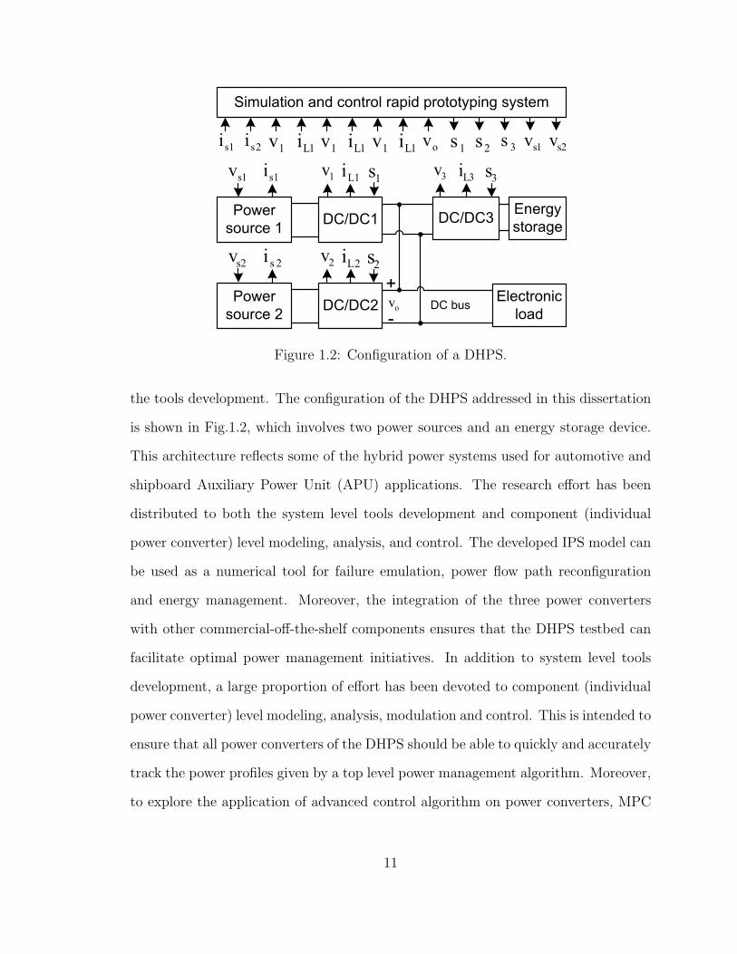
1v
ov DC bus
1Li1sv 1si
2v 2Li2sv 2si
3v 3Li1s
2s
3s1si 2si 1v 1Li 1v 1Li 1v 1Li 1s 2s 3s 1sv 2svov
Figure 1.2: Configuration of a DHPS.
the tools development. The configuration of the DHPS addressed in this dissertation
is shown in Fig.1.2, which involves two power sources and an energy storage device.
This architecture reflects some of the hybrid power systems used for automotive and
shipboard Auxiliary Power Unit (APU) applications. The research effort has been
distributed to both the system level tools development and component (individual
power converter) level modeling, analysis, and control. The developed IPS model can
be used as a numerical tool for failure emulation, power flow path reconfiguration
and energy management. Moreover, the integration of the three power converters
with other commercial-off-the-shelf components ensures that the DHPS testbed can
facilitate optimal power management initiatives. In addition to system level tools
development, a large proportion of effort has been devoted to component (individual
power converter) level modeling, analysis, modulation and control. This is intended to
ensure that all power converters of the DHPS should be able to quickly and accurately
track the power profiles given by a top level power management algorithm. Moreover,
to explore the application of advanced control algorithm on power converters, MPC
11

schemes of the FBC also have been investigated to achieve voltage regulation without
peak current violation. This paves the way for the future system-level advanced
control algorithm development.
1.2.2 Contributions
This dissertation has focused on modeling, analysis and control of DC hybrid
power systems. The contributions of this dissertation are summarized as follows:
• A DHPS testbed has been built at the Realtime Advanced Control Engineer-
ing Lab at the University of Michigan to provide the research infrastructure to
support the power management for all electric ships. The testbed consists of
a digital simulation and control rapid prototyping platform, two unidirectional
FBCs, a bidirectional DABC, two programmable power sources, two program-
able loads, and a supercapacitor based energy storage bank. This DHPS testbed
facilitates system level analysis, optimization and control of a DC hybrid power
system of an AES.
• A modularized simulation model for an IPS of an AES is developed. The IPS
model has power generation modules including a gas turbine and a fuel cell
power system, two electric propulsion modules and a zonal electric distribution
system which, by itself, has many power conversion modules. The simulation
results verify that the IPS model can be used for failure emulation, power flow
path reconfiguration and energy management. This model provides an effective
tool for AES system research.
• A new power flow model for a DABC over a wide operating range is developed.
In addition to those major parameters used by conventional power flow analysis,
this new model incorporates minor parameters, namely the power semiconduc-
12

tor voltage loss and dead time. The minor parameters are critical for explaining
the observed internal power transfer and phase drift phenomena, which are rele-
vant to power flow characterization of the DABC. While the new model provides
a more accurate prediction over a wide range of operating conditions, it also
identifies new characteristics such as reverse power transfer and energy sink that
are observed in experiments. Therefore, the new model can serve as a research
tool for optimal hardware design, operating range selection and power manage-
ment strategy development. The experimental results illustrate the effectiveness
of the new model.
• A current-mode PWM modulation strategy for a dual active bridge DC/DC
converter is developed. The proposed modulation strategy can avoid the draw-
backs of the conventional phase shift modulation and achieve: (1) zero circulat-
ing current to reduce conduction loss; (2) soft-switching over the full operating
range to reduce switching loss; (3) zero idling power to eliminate idle loss; (4)
simple but accurate power flow characterization; and (5) controllable output
power between zero and the maximum for different combinations of terminal
voltages. Moreover, the proposed modulation strategy enables the converter to
achieve the same power density under the same current stress as that of a phase
shift modulated converter. Therefore, in comparison with the traditional ones,
the proposed strategy is more suitable for energy storage system application.
• The MPC schemes are employed to control the FBC. The MPC schemes can
achieve voltage regulation without violating a peak current constraint. Compar-
ative evaluation of LMPC and NLMPC schemes for a FBC is performed. The
computation time and closed loop system performances under starting, overload
and load step change conditions are compared. The experimental results reveal
13

that both the LMPC and NLMPC schemes can successfully achieve voltage
regulation and peak current protection. Considering the algorithm complexity,
the closed loop performance and the necessary computation time, we conclude
that the NLMPC scheme is more desirable than the LMPC for this application.
To the best knowledge the author, this is the first implicit MPC application
reported in open literature for a DC/DC power converter with a millisecond
level time constant.
1.3 Dissertation Overview
The dissertation is organized into eight chapters. The first chapter introduces the
background, research scope and contributions of this dissertation. The second and
third chapters develops tools for the DHPS and IPS of an AES. The fourth and fifth
chapters present a novel power flow model and develop a new modulation strategy
to improve the power control performance for the FBC. The sixth chapter presents
the experimental results that validate the power tracking capability of the DHPS.
The seventh chapter develops and compares MPC schemes for the FBC. The final
chapter summarizes results and outlines future research work. The remainder of the
dissertation is organized as follows:
Chapter 2 develops a testbed for a DC hybrid power system. The major components
of this testbed, including the realtime simulation and control rapid prototyp-
ing platform, the isolated unidirectional and bidirectional DC/DC converters,
the programmable power sources, the programmable electronics loads and the
supercapacitor based energy storage bank are introduced.
Chapter 3 introduces a simulation model for the IPS of an AES. Different subsys-
tems of the IPS model are first developed. A LabVIEW based graphic user
14

interface is then presented. Finally, the simulation results verify that the IPS
model can be used to perform simulations for scenarios such as failure emulation,
power flow path reconfiguration and energy management.
Chapter 4 presents a novel power flow model for the DABC. The conventional power
flow analysis is first introduced. Then, the effects of minor parameters such as
the power semiconductor voltage loss and dead time are investigated. Based
on the analysis, a new power flow model is then developed. The model can
accurately predict the power flow over a wide operating range. The experimental
results confirmed the effectiveness of the new model.
Chapter 5 develops a novel current mode PWM strategy for the DABC. The mod-
ulation strategy is first introduced. Then, the characteristics of the power con-
verter modulated by the new strategy are analyzed. Finally, the experimental
results confirm the superior performance of the dual active converter modulated
by the proposed new modulation strategy.
Chapter 6 presents the experimental results that validate the power tracking ca-
pability of the DHPS. The power controllers are designed to track the power
profile provided by the top level power management algorithm. The experi-
mental results reveal that the designed controllers can track the power profiles
quickly and closely.
Chapter 7 develops the MPC schemes for voltage regulation control of the FBC and
compares linear and nonlinear MPC schemes. First, the peak current protection
constraint is derived. Then, the dynamic model of the FBC is developed, based
on which a nonlinear observer is designed for state and parameter estimation.
After that, offset-free linear MPC and nonlinear MPC problems are formulated,
15

followed by an introduction of the InPA-SQP algorithm. Finally, the computa-
tion time and closed loop performance of the LMPC and NLMPC are compared
through experimental tests.
Chapter 8 presents conclusions and outlines future research plans.
16

Chapter 2
DC Hybrid Power System Testbed Development
As a large scale complex system, the IPS encompasses power generation, distri-
bution, propulsion and ship service loads. Subsystems involved in IPS range from
thermal power plants such as diesel engine or gas turbine, to propulsion motor and
power electronic converters that are switching at over kilo-Hz rate. Intricate dy-
namic interactions among subsystems, in the form of thermal dynamic, electrical,
mechanical, and chemical, often dictate the dynamic performance and operational
integrity of the overall system. When the system is undergoing transients, managing
the inter-connectivity of the power network and leveraging the interactions among
diverse power plants/loads become a critical task for the shipboard power manage-
ment systems. Along with the opportunities ushered in by the IPS systems, the
inter-connectivity and complexity of the IPS represent a major system design and
optimization challenge, calling for the development of effective analytical frameworks
and numerical tools.
This dissertation focuses on the modeling, analysis, and control of a DC Hybrid
Power System (DHPS). However, it is unrealistic to build a full scale DHPS in a uni-
versity setting. Therefore, in order to address the challenges imposed by coordinating
17
control of multiple power converters of the DHPS, such as the wide range of operat-
ing conditions, the requirements for fast power response and load following and the
stringent constraints of high system reliability, it is necessary to develop a testbed to
facilitate system level analysis, optimization and control. Such a testbed should have:
(1) fully digital simulation capability as a preliminary analysis tool to support the
modeling and control development effort, (2) adequate hardware resources for con-
trolling a complex dynamic system, (3) necessary hardware, including power sources,
power converters and loads, to verify analysis, modeling and evaluation results. Fi-
nally, it should have control rapid prototyping capability to ensure quick implemen-
tation of advanced control algorithms for system performance evaluation and design
validation. In this chapter, a DHPS testbed which has the aforementioned functions
will be presented.
2.1 DHPS Testbed Development
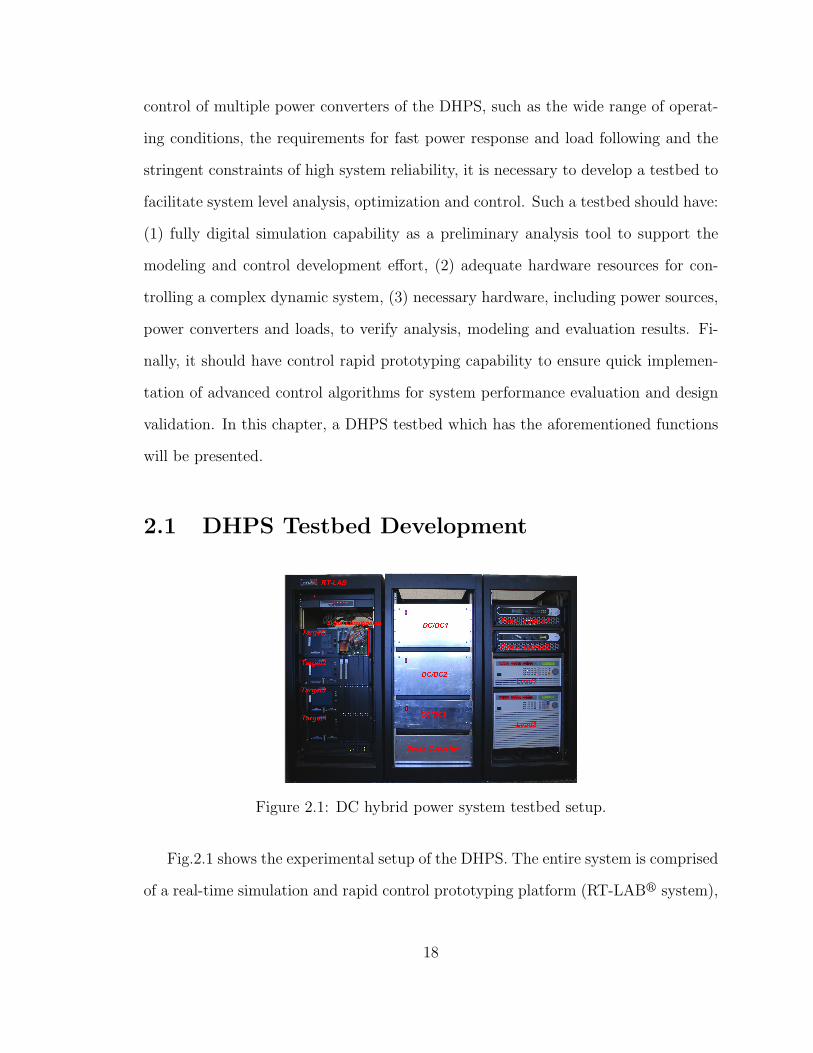
Figure 2.1: DC hybrid power system testbed setup.
Fig.2.1 shows the experimental setup of the DHPS. The entire system is comprised
of a real-time simulation and rapid control prototyping platform (RT-LABr system),
18
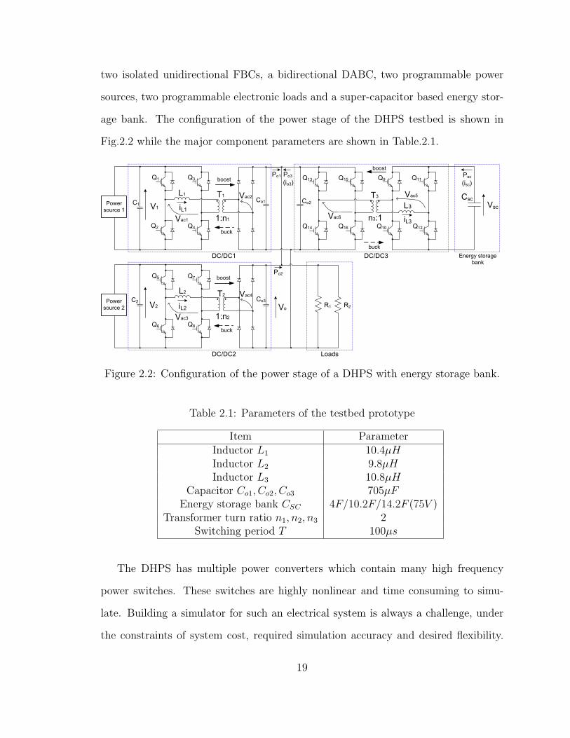
two isolated unidirectional FBCs, a bidirectional DABC, two programmable power
sources, two programmable electronic loads and a super-capacitor based energy stor-
age bank. The configuration of the power stage of the DHPS testbed is shown in
Fig.2.2 while the major component parameters are shown in Table.2.1.
Q9
Q10 Q12
L3
n3:1
Q11
Vo
Q16
Q15
Vsc
Q13
Q14
iL3
Q1
Q2 Q4
L1
1:n1
Q3
V1 iL1Power
source 1
T1
Q5
Q6 Q8
L2
1:n2
Co3
Q7
iL2
T2
T3C1
V2Power
source 2C2
Co1 Co2Csc
DC/DC1
DC/DC2
DC/DC3 Energy storage bank
Loads
R1 R2
Vac1
Vac2
Vac3
Vac4
Vac6
Vac5
PscPo3Po1
Po2
(io3) (isc)boost
buck
boost
buck
boost
buck
Figure 2.2: Configuration of the power stage of a DHPS with energy storage bank.
Table 2.1: Parameters of the testbed prototype
Item ParameterInductor L1 10.4µHInductor L2 9.8µHInductor L3 10.8µH
Capacitor Co1, Co2, Co3 705µFEnergy storage bank CSC 4F/10.2F/14.2F (75V )
Transformer turn ratio n1, n2, n3 2Switching period T 100µs
The DHPS has multiple power converters which contain many high frequency
power switches. These switches are highly nonlinear and time consuming to simu-
late. Building a simulator for such an electrical system is always a challenge, under
the constraints of system cost, required simulation accuracy and desired flexibility.
19

In contrast with an analog simulator, which achieves real-time simulation by using
scaled down analog models of actual components, a digital simulator is becoming
popular due to its low maintenance cost and flexibility. Many offline simulation pack-
ages including MATLAB/Simulinkr, PLECSr, SABERr, etc., can perform offline
simulation, but they either can’t interact with external hardware or their simula-
tion speed is too slow for large scale system simulation. Real-time digital simulators
are a promising approach since they avoid those drawbacks. In comparison with
DSP and FPGA based real-time simulators, the PC cluster based simulation sys-
tem would be a better choice considering the low hardware cost, high simulation
performance as well as the flexibility provided by the modular system architecture.
RT-LABr is a PC-cluster based expandable real-time simulator which is compatible
with Matlab/Simulinkr, thereby allowing effective leverage of commercially avail-
able MATLAB/Simulinkr toolsets, such as control system design and analysis tool-
boxes,code generation toolboxes, and Physical Modeling toolboxes. Specialized tools
such as ARTEMISr and RT-Eventsr support multi-rate fixed-time-step real-time
simulation of power systems with dramatically improved computation speed and ac-
curacy [7].
Fig.2.3 shows the configuration of the real-time simulation platform while its hard-
ware is shown in Fig.2.1 (left rack). This system has 8 CPUs allocated in 4 physically
separated targets. The CPUs in the same target exchange information through the
shared memory while the different targets communicate through infiniband switch
with 10Gb/s speed. There are three host PCs which can talk with each target via
1Gb/s Ethernet switch. The targets can interact with the external hardware through
32bits PCI Bus I/O interfaces. Combining the FPGA event detection with special-
ized real-time interpolation algorithms toolbox RT-Eventsr, the effective precision of
the I/O could be better than 1µs. The I/O interface provides a platform for data
20
Figure 2.3: RT-Lab real-time simulation system configuration.
acquisition and signal conditioning modules that enable the implementation of high
frequency analog/digital I/O, event capture, and event generation. All of the targets
and CPUs are synchronized either by software or by hardware. Thus all of the CPUs
can synchronously interact with the analog and digital I/O. This feature makes it
possible for the system to implement physical components for hardware-in-the-loop
simulation or to perform control prototyping experiments. In addition, the synchro-
nized targets can run real-time simulations at different time steps, making it very
flexible to distribute the complex model to different targets or CPUs within the sim-
ulation platform. This real-time simulator also can interact with other stand alone
RT-Lab targets through Ethernet. For our testbed, the RT-LABr system serves the
following three functions: (1) as a real-time simulator to simulate power source mod-
els and to control programmable power supplies to emulate the characteristics of a
specified power source; (2) as an embedded controller for which the C code generated
in a host PC can be downloaded and executed in target CPUs to control power con-
21
verters; (3) as a data acquisition device to sample and store experimental data for
feedback control and detailed offline analysis.
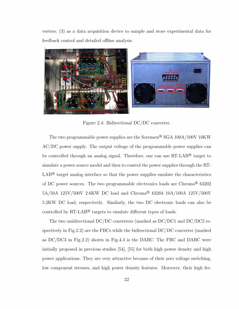
Figure 2.4: Bidirectional DC/DC converter.
The two programmable power supplies are the Sorensenr SGA 100A/100V 10KW
AC/DC power supply. The output voltage of the programmable power supplies can
be controlled through an analog signal. Therefore, one can use RT-LABr target to
simulate a power source model and then to control the power supplies through the RT-
LABr target analog interface so that the power supplies emulate the characteristics
of DC power sources. The two programmable electronics loads are Chromar 63202
5A/50A 125V/500V 2.6KW DC load and Chromar 63204 10A/100A 125V/500V
5.2KW DC load, respectively. Similarly, the two DC electronic loads can also be
controlled by RT-LABr targets to emulate different types of loads.
The two unidirectional DC/DC converters (marked as DC/DC1 and DC/DC2 re-
spectively in Fig.2.2) are the FBCs while the bidirectional DC/DC converter (marked
as DC/DC3 in Fig.2.2) shown in Fig.4.3 is the DABC. The FBC and DABC were
initially proposed in previous studies [54], [55] for both high power density and high
power applications. They are very attractive because of their zero voltage switching,
low component stresses, and high power density features. Moreover, their high fre-
22
quency transformer prevents fault propagation and enables a flexible output/input
voltage ratio. Therefore, with a FBC or a DABC as the power conditioning system,
the low voltage high current power source such as the fuel cell power system and
energy storage device can be applied to high DC voltage applications, such as the DC
zonal electrical distribution system of an all electric ship [93].
The energy storage bank is composed of two branches of super-capacitors. One
branch includes five BOOSTCAPr BPAK0020-15V modules which are connected
in series and offer total 4F capacitance. The other branch has five BOOSTCAPr
BPAK0052-15V modules, therefore it provides 10.2F capacitance. Both the two
branches have a 75V working voltage. Moreover, they can be connected in parallel to
provide 14.2F capacitance. Therefore, the energy storage bank can be reconfigured
for different applications.
While the RT-LAB system enables the control rapid prototyping of the DHPS
which has multiple power converters, its multi-target multi-rate structure facilitates
realtime simulation of a large scale system, such as the IPS of an AES. In parallel
with hardware construction, a modularized simulation model of an IPS is developed
and will be introduced in Chapter 3.
2.2 Summary
In this Chapter, a DHPS testbed is introduced. The testbed is built at the Univer-
sity of Michigan and has all of the necessary functions specified in the first paragraph
of this chapter, thereby facilitating optimization and power management strategy de-
velopment for the DHPS. Leveraging the realtime simulation capability of the testbed,
a modularized simulation model for an IPS of an AES is developed and the realtime
simulation results will be presented in the next chapter.
23
Chapter 3
Modeling and Simulation of an Integrated Power
System for an All Electric Ship
In this chapter, a modularized model for an Integrated Power System (IPS) of
an All Electric Ship (AES) is developed. All major subsystems of the model are
first introduced. Then, the model integration and distribution method is presented.
Finally, the graphical user interface is demonstrated, followed by the simulation results
for scenarios such as failure emulation, power flow path reconfiguration and energy
management.
3.1 Modeling of IPS
Since the IPS is a large scale power system containing many high frequency power
switches or other components whose simulation is very resource demanding, it is time
consuming to simulate and debug such a large system offline. On the other hand,
parameter tuning of this complex system as a whole is a daunting, if not impossible,
task. Furthermore, many of the subsystems in Zonal Electrical Distribution System
(ZEDS) are similar and can be reused. Therefore, our effort is focused on developing
24
a modularized IPS model for AES application. We split the whole IPS into three
subsystems, namely the Power Generation Module (PGM) including a gas turbine
and fuel cell power system, Electric Propulsion Module (EPM), and ZEDS. ZEDS,
by itself, consists of many power conversion modules and electric loads.
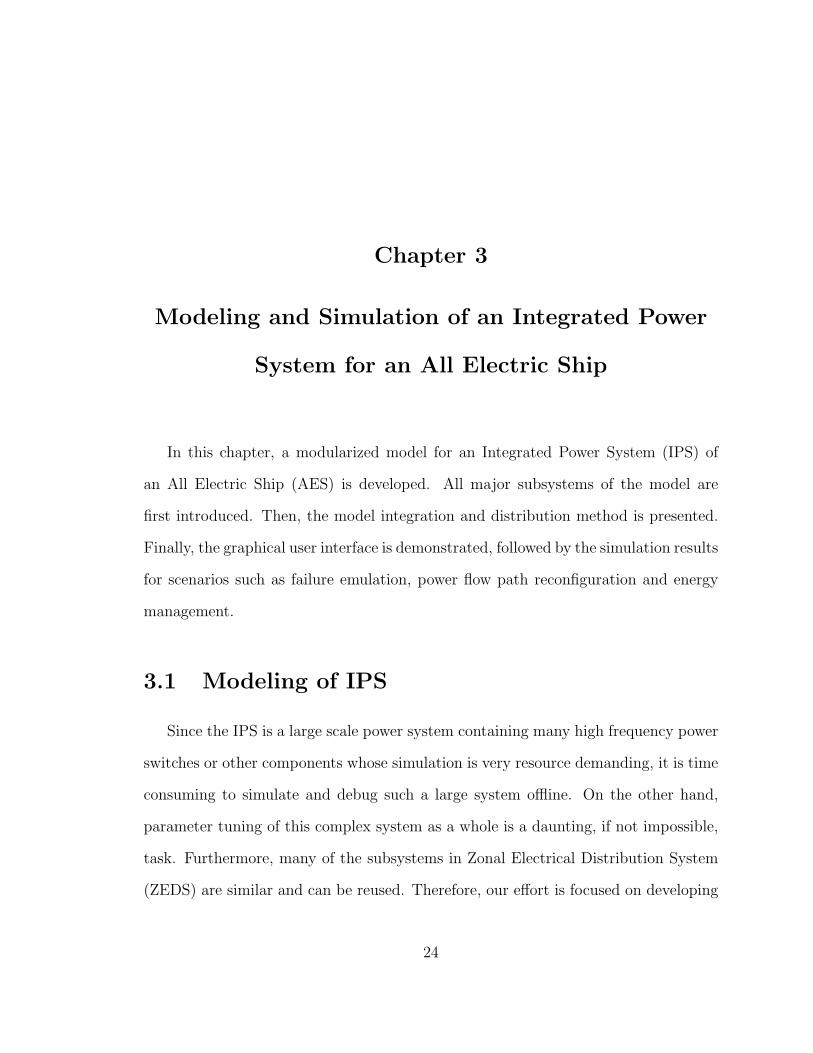
3.1.1 Gas Turbine Module
While many different types of power systems are used for shipboard applications,
gas turbine/generator sets are quite often used as the shipboard prime mover. A
combination of first principles and empirical relationships have been used for the gas
turbine model development [102]. The schematic of the gas turbine model developed
for the ship-board power system is shown in Fig. 3.1.
Figure 3.1: Schematic of the gas turbine/generator system.
The gas turbine model captures the dynamic characteristics of compressor, tur-
bine, combustor and the coupling between turbine and compressor. The combustor
mass and temperature dynamics along with turbocharger rotational dynamics are
considered, while the compressor and turbine air mass flows and efficiencies are mod-
eled as empirical relations. The input to the gas turbine is assumed to be JP5 fuel
flow injected into combustor, and the torque input on the turbocharger shaft, reflect-
25

ing the power demand, is the disturbance to the turbine operation. The variables and
parameters used in GT model are defined in Table 3.1. The following standard [102]
assumptions have been made for the gas turbine model.
• The heat loss in the compressor is negligible.
• Compression and expansion process are adiabatic.
• Fuel injector dynamics are faster as compared to the burner temperature and
mass dynamics and are neglected.
• Perfect combustion occurs inside the burner.
• The generator is modeled as an efficiency transfer function from mechanical
power input to electrical power output.
Under these assumptions, the equations representing the dynamics can be derived
using first principles, such as energy, mass and power balance and curve fitting as
follows:
Compressor and Turbine
The compressor and turbine mass flow and the isentropic efficiency (Appendix
A) are obtained by curve fitting the performance maps scaled from an automotive
application [103] using the techniques suggested in [104], [105]. They are functions of
pressure ratio ( pbpamb
), combustor temperature (Tb) and the turbocharger speed (ωtc)
The compressor power is determined using the first law of thermodynamics and
is given by
Pc = Wccp(Tc,out − Tamb), (3.1)
26
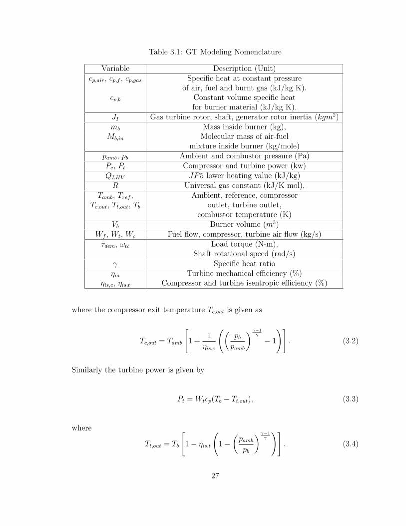
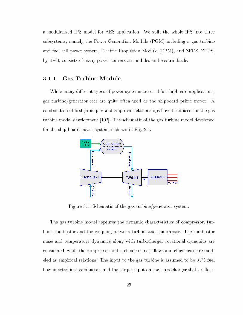
Table 3.1: GT Modeling Nomenclature
Variable Description (Unit)cp,air, cp,f , cp,gas Specific heat at constant pressure
of air, fuel and burnt gas (kJ/kg K).cv,b Constant volume specific heat
for burner material (kJ/kg K).JI Gas turbine rotor, shaft, generator rotor inertia (kgm2)mb Mass inside burner (kg),Mb,in Molecular mass of air-fuel
mixture inside burner (kg/mole)pamb, pb Ambient and combustor pressure (Pa)Pc, Pt Compressor and turbine power (kw)QLHV JP5 lower heating value (kJ/kg)R Universal gas constant (kJ/K mol),
Tamb, Tref , Ambient, reference, compressorTc,out, Tt,out, Tb outlet, turbine outlet,
combustor temperature (K)Vb Burner volume (m3)
Wf , Wt, Wc Fuel flow, compressor, turbine air flow (kg/s)τdem, ωtc Load torque (N-m),
Shaft rotational speed (rad/s)γ Specific heat ratioηm Turbine mechanical efficiency (%)
ηis,c, ηis,t Compressor and turbine isentropic efficiency (%)
where the compressor exit temperature Tc,out is given as
Tc,out = Tamb
[1 +
1
ηis,c
((pbpamb
) γ−1γ
− 1
)]. (3.2)
Similarly the turbine power is given by
Pt = Wtcp(Tb − Tt,out), (3.3)
where
Tt,out = Tb
[1− ηis,t
(1−
(pambpb
) γ−1γ
)]. (3.4)
27
Combustor
The burner mass is determined using the mass balance and is given by
mb = Wf +Wc −Wt (3.5)
and the temperature is determined using energy balance as
Tb =1
mbcv,b((Wccp,air +Wfcp,f )(Tc,out − Tref )
+WfQLHV −Wtcp,gas(Tb − Tref )) −
cv,b(Tb − Tref )mb) . (3.6)
The burner pressure pb is derived using the ideal gas law:
pb =mb
Mb,inVb(RTb). (3.7)
Output Shaft Speed
The shaft speed is determined using the power balance on the shaft given by
ωtc =1
JI
(ηmPt − Pc
ωtc− τdem
). (3.8)
The gas turbine drives the power generation device which converts mechanical
power to electrical power and generates three-phase AC power with 4160V line to
line voltage and 60Hz frequency. For the particular system modeled in this platform,
the total power output is between 255 KW to 1.4 MW. The open loop simulations
for step changes in power demand are shown in Fig. 3.2 and the gas turbine has a
rapid response that can be captured by a second order dynamical system.
28
0 5 10 15 20 25 30 35450
500
550
600
650
700
750
800
850
900
time sec
Pow
er K
W
Open Loop Simulation of Gas Turbine Model
Pdem
PGT/gen
Figure 3.2: Open loop simulations of gas turbine: demand Vs. generated power.
Figure 3.3: Schematic of fuel processing system
3.1.2 Fuel Cell and Reforming Unit Module
The Fuel Cell (FC), which is clean and highly efficient, is considered as an auxiliary
power source for the IPS. We consider a Polymer Electrolyte Membrane (PEM) fuel
cell along with a fuel processing system (FPS). The FPS+FC (Figure 3.3) system
consists of a hydro desulphurizer (HDS), heat exchanger (HEX), mixer (MIXER),
fuel reformer (FR), water gas shift reactor (WGS) and fuel cell anode dynamics. A
detailed 10 state model of the FPS+FC system has been developed in [106]. The effort
here was to develop a reduced order model that still captures the system dynamics
29

as well as operating constraints such as fuel starvation. Based on the linear analysis
of the 10 state model around different operating points, we found that the dominant
modes corresponded to the FR temperature, HDS and the anode hydrogen partial
pressure. Therefore our reduced order model has three states. The inputs to the
FPS+FC are fuel and air flow, while the stack current is considered as a disturbance.
The variables and parameters used in FC model are defined in Table 3.2. The
following assumptions were made for the simplified FC+FPS model.
• Due to the relatively large volume of the reformer, we assume that the dy-
namics associated with the fuel path are slower than those with the air path.
Consequently, the cathode dynamics are neglected.
• WGS reactions are fast and perfectly controlled and hence the dynamics are
neglected.
• The temperature inside the fuel cell is assumed to be controlled to remain
constant.
Since the stack current (Ist) is measured, the fuel and air flow are determined by
a static feedforward map to control the steady state fuel utilization (UH2) to 0.8 as
given in [106].
Hydro Desulphurizer
The HDS is represented as a large volume and is simplified as a first order lag with
a slow time constant (τHDS = 5sec) that reflects the slow dynamics of the linearized
model given in [106]. The other two states representing slow dynamics in [106] are
the FR temperature and the anode hydrogen partial pressure.
30

Table 3.2: FC Modeling Nomenclature
Variable Description (Unit)cp,FR Ratio of constant specific heat
of FR material (kJ/kg K)E Open circuit fuel cell voltage
hin, hout Specific enthalpy (J/kg) of inletand outlet FR flows
mFR, Mass inside the reformer unit (kg)Man, MH2 Molecular mass of anode material
and hydrogen(kg/mol)nc Number of fuel cells in the stack
Nin, Nout Molar flow rates in and out of the FR (mol/s)pan,pH2,an Anode total and hydrogen partial pressure (Pa)
R Universal gas constant (J/K mol)TFR, Tan FR and anode temperature (K)
vohm, vact, vconc Ohmic, activation andconcentration loss respectively (volt)
Van Anode volume (m3)WFR,in Total flow into the FR (kg/s)
WFR,H2 , WFR,out Hydrogen and total flow out of FR (kg/s)WH2,react Reacted hydrogen inside anode (kg/s)
WH2,an, Wan Hydrogen and total anode exit flow (kg/s)
Fuel Reformer
The FR model is developed in [106] and is summarized here. The temperature
dynamics using energy balance is given by
dTFRdt
=1
mFRcp,FR[Ninhin −Nouthout] (3.9)
where the inlet flow consists of the fuel and air flow and the outlet flow includes the
following species: CH4, CO, CO2, H2, H2O, N2.
31
Anode
The anode partial pressure dynamic using mass balance is given by
dpH2,an
dt=
RTanMH2Van
(WFR,H2 − χanH2Wan −WH2,react),
χanH2=
(MH2
Man
)(pH2,an
pan
), (3.10)
where WFR,H2 is the hydrogen flow from the reformer, Wan, WH2,react are the anode
outlet flow and reacted hydrogen. The anode outlet flow is given by the orifice
equation as,
Wan = W0,an
√pan − pamb
∆p0
,
where ∆p0 is the pressure drop across the orifice with ∆p0 = 600Pa as given in [106].
The hydrogen consumed is given by the electrochemistry principle as follows:
WH2,react = MH2
ncIst2F
.
where n is the number of cells (1000) and F is Faraday constant. The air supply is
assumed to be instantaneous and the cathode pressure follows the anode pressure.
Stack Voltage Model
The stack voltage is a function of the fuel cell temperature and pressure and is
given by vst = nc(E − vact − vohm − vconc) and further details of this model can be
obtained from [106].
The output of the FC system is connected to the DC-Link in PCM4 through a
DC/DC converter. For the particular system modeled, the total power output of the
32
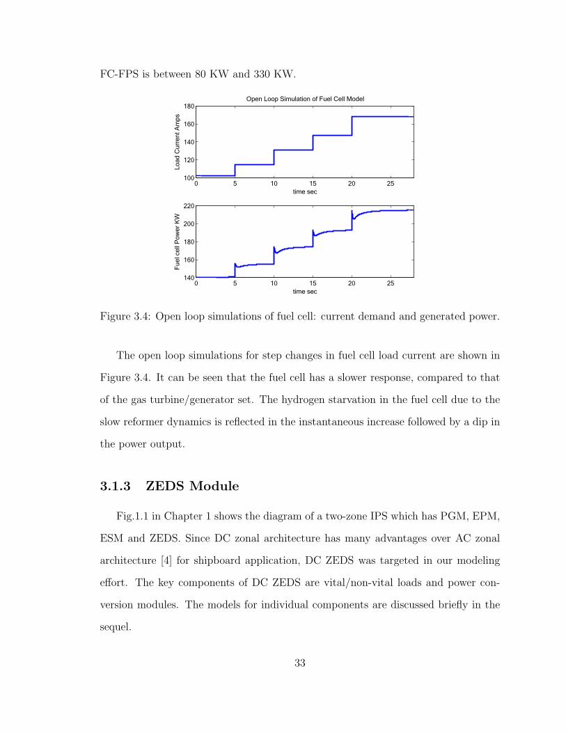
FC-FPS is between 80 KW and 330 KW.
0 5 10 15 20 25100
120
140
160
180
time sec
Load
Cur
rent
Am
ps
Open Loop Simulation of Fuel Cell Model
0 5 10 15 20 25140
160
180
200
220
time sec
Fue
l cel
l Pow
er K
W
Figure 3.4: Open loop simulations of fuel cell: current demand and generated power.
The open loop simulations for step changes in fuel cell load current are shown in
Figure 3.4. It can be seen that the fuel cell has a slower response, compared to that
of the gas turbine/generator set. The hydrogen starvation in the fuel cell due to the
slow reformer dynamics is reflected in the instantaneous increase followed by a dip in
the power output.
3.1.3 ZEDS Module
Fig.1.1 in Chapter 1 shows the diagram of a two-zone IPS which has PGM, EPM,
ESM and ZEDS. Since DC zonal architecture has many advantages over AC zonal
architecture [4] for shipboard application, DC ZEDS was targeted in our modeling
effort. The key components of DC ZEDS are vital/non-vital loads and power con-
version modules. The models for individual components are discussed briefly in the
sequel.
33

Power Conversion Module1 (PCM1)
From PCM4
DC busDC bus
To subbus
2Vo
1Io
6Vp4-
5Vp4+
4Vb2-
3Vb2+
2Vo-
1Vo+
v+ -V1
c Io
1+
1-
2+
2-
Switch3
c
1+
1-
2+
2-
Switch2
c
1+
1-
2+
2-
Switch1
g
+
-
A
gnd
SPS Compatible 1-legTime Stamped Bridge
R1
L1
Vref
Vf dbkPulses
Controller
Vo
C1
3S3
2S2
1S1
Figure 3.5: SimPowerSystems/ARTEMIS model of PCM1 in ZEDS.
Fig.3.5 shows the model of PCM1. PCM1 is a step down DC/DC converter with
three reconfigurable switchboards. The step down DC/DC converter is modeled with
the 1-leg Time-Stamped Bridge of the ARTEMISr toolbox while other components
are modeled with SimPowerSystemsr toolbox. Manipulating the three switchboards
can reconfigure the power flow path of each electric zone. DC bus failure and recovery
emulation also can be achieved by the manipulation of switchboards. The output
voltage of PCM1 is 900VDC which is 200V less than the main bus. The loads of
PCM1 are one nonvital load and one vital load under normal situations. One vital
load will be added if the opposite main bus or PCM4/PCM1 is down because of either
equipment failure or battle damage.
PCM2/5 (DC/AC inverter for vital load)
Fig.3.6a shows the diagram of PCM2/5. PCM2/5 is a DC/AC inverter which
is modeled with SimPowerSystemsr Compatible 3-leg Time-Stamped Bridge of the
ARTEMISr toolbox. Since they energize the vital load which shouldn’t lose power
34

AC BusPort Bus
STBD BusFuel Cell
AC/DC(rectifier)
DC/DC DC/DC
DC-Link
Upper input
Load
ABTLower input
DC/AC Input LoadDC/DC
DC/DC
(b)(a)
(c)
Figure 3.6: Diagram of PCMs in ZEDS.
by any chance, there is an Auto Bus Transfer (ABT) circuit which can automatically
select power input port between the upper input and lower input. Usually the upper
input has higher priority than the lower one and will be dropped only when its voltage
decreases to 100V lower than the lower input. However, to balance load for the two
DC buses, the upper input will take over again if its voltage is recovered to 50V higher
than the lower input.
PCM3/6 (DC/DC converter for non-vital load)
Fig.3.6b shows the diagram of PCM3/6 which also is DC/DC converter. In
comparison with PCM1, PCM3/6 doesn’t have switchboards for load redirection.
PCM3/6 is modeled with the 1-leg Time-Stamped Bridge of the ARTEMISr toolbox
too. There is no ABT in PCM3/6 given the nonvital nature of the loads connected
to it. The nonvital load will directly lose its power if the main bus or sub-bus on its
side is down.
35

PCM4
Fig.3.6c is the diagram of PCM4 which conventionally is an AC/DC converter
converting three-phase AC power to DC power by controlling the rectifier firing angle.
For our model, PCM4 has hybrid power sources, AC main bus and fuel cell, the
output of AC/DC was connected with output of the DC/DC converter of fuel cell
model through DC-Link. The proportion of power drawn from AC bus and fuel cell
respectively can be dynamically managed by splitting the desired current to the two
input converters. To get well regulated DC voltage on the port bus and starboard bus,
there are starboard side and port side output DC/DC converters drawing power from
DC-Link and regulating the voltage on the two DC buses to 1100VDC. The modeling
of the two output DC/DC converters is similar to the DC/DC converter in PCM1, the
buck converter topology is adopted and modeled with SimPowerSystemsr compatible
1-leg Time-Stamped Bridge of the ARTEMISr toolbox. Both of the output converters
are regulated by their dedicated PI controller.
Loads
Vital/nonvital loads were modeled as constant power loads. All of the loads can
draw a certain amount of power from the DC bus according to commands from the
energy management module. More detailed load models such as those for DC motor
or AC motor also could be modeled and integrated in the future.
3.1.4 Propulsion Module
Electric Propulsion System Model
The electric propulsion system model is a three-phase AC/DC/AC variable speed
transmission system with the low speed, high torque Permanent Magnet Synchronous
36

Motor (PMSM) driving the propeller. The AC/DC rectifier is modeled with SimPowerSystemsr
toolbox Universal Bridge. There is also a braking chopper on the DC-Link to absorb
the regenerated energy by the motor at the crash stop situation. The DC/AC inverter
which works as the frequency converter and drives the propulsion PMSM is modeled
with Time-Stamped Bridge of the ARTEMIS toolbox and controlled by a close loop
speed controller. Other than the three-phase AC/DC/AC propulsion system, other
AC propulsion technologies such as cyclo-convertor [10], matrix converter [14] and
high temperature superconductor (HTS) motor [15] also can be modeled and inte-
grated into the propulsion module in the future.
Ship Dynamic Model
The load torque to the eletric propulsion motor is determined by the ship dynamic
model, which calculates the ship speed and propeller speed according to hydrody-
namics. The ship model given in [16] is adapted. It includes the added mass and
hydrodynamic forces and moments acting on the ship. Given a desired ship speed,
the desired motor speed and torque are calculated in this module and fed to the
propulsion motor control unit.
3.2 Model Integration, Distribution and Prelimi-
nary Simulation
3.2.1 Model Integration and Distribution
There are two stages for the IPS model integration. First of all, the ZEDS module
and propulsion module are integrated and tested respectively. As we discussed in
the previous sections, the key components of ZEDS, loads and PCMs, are separately
37

developed and tested. After that, all of the PCMs and loads are interconnected
to form the two zones of the ZEDS. The integration of ship dynamic model and
propulsion model is quite straightforward too. The desired propeller torque and
speed signals which are calculated by ship dynamic model are sent to the motor in
the propulsion model. Then ZEDS and propulsion modules are connected with the
power generation module.
The IPS is a large scale system which has many subsystems with different charac-
teristics. For example, the dynamics of G/T and FC are relatively slow, and sampling
at 1ms time step is sufficient. On the other hand, PCMs have high frequency power
switches, the subsystem time step is 50µs in our case which is much shorter than
PGMs’. To get a relatively balanced computation task distribution among all CPUs
for better simulation performance, one has to distribute the model properly into the
8-CPU simulator. There are several considerations that need to be taken into account
in allocating resources: (1) The subsystems assigned to each CPU should assume that
no overruns will result, otherwise simulation performance will be compromised; (2)
Since real-time communication between targets is a resource demanding process, it
is advantageous to assign a modularized subsystem as one entity to one CPU in-
stead of splitting the subsystem into several parts to reduce the number of signals
to be exchanged between targets; (3) Each CPU can run real-time simulation with
one sampling rate, subsystems with slow sampling speed can be grouped with the
subsystem with fast sampling speed. Given these constraints, we assign one CPU for
subsystems PGM(Gas Turbine), PGM(Fuel Cell) and EPM while splitting the ZEDS
into two subsystems with two associated CPUs.
Another challenge for model distribution is that all of the distributed subsys-
tems exchange information through the RT-LAB block-OpComm, which is only com-
patible with arrowlines. Arrowline indicates the unidirectional signal flow and is
38

the default connection for Simulinkr as well as many Simulinkr compatible tool-
box blocks. However, the power conversion and propulsion subsystems developed
with SimPowerSystemsr toolbox use stublines by default. The stubline passes sig-
nals bidirectionally just as a physical wire would do. The incompatibility between
SimPowerSystemsr sub models and OpComm blocks is resolved by DC and AC bus
models which convert the signals flow on the stubline into signals flow on the arrow-
line. These bus models are incorporated to appropriate locations where it is necessary
to split the model and assign different CPUs to the subsystems.
Based on the integrated model, simulations were performed which will be discussed
in the following subsection.
3.2.2 Preliminary Simulations
To validate the IPS model of an AES, realtime simulation was performed on the
RT-LAB system. The IPS has a main power generation system, namely a gas turbine
generator set, which can deliver power up to 1.4MW. The auxiliary power generation
system is a fuel cell power system which can provide up to 330KW power for the ship
service loads. The rated power of the electrical propulsion system is 1.3MW which
can drive the model ship with a ten-knot speed. The goals of the simulations are to
validate the transient response, failure emulation and power flow path reconfiguration
capability of the IPS model.
Fig.3.7 shows power consumed by loads during a failure and reconfiguration pro-
cess where four scenarios are represented. Scenario 1: the port bus or local PCM1/PCM4
is down, the non vital load loses its power while the vital load draws power from the
STBD bus. Scenario 2: the port bus is reconfigured or the PCM1/PCM4 is recovered,
all loads draw equally 40KW power from both buses. Scenario 3: the STBD bus is
down which leads to the STBD side nonvital load losing its power. The vital load
39
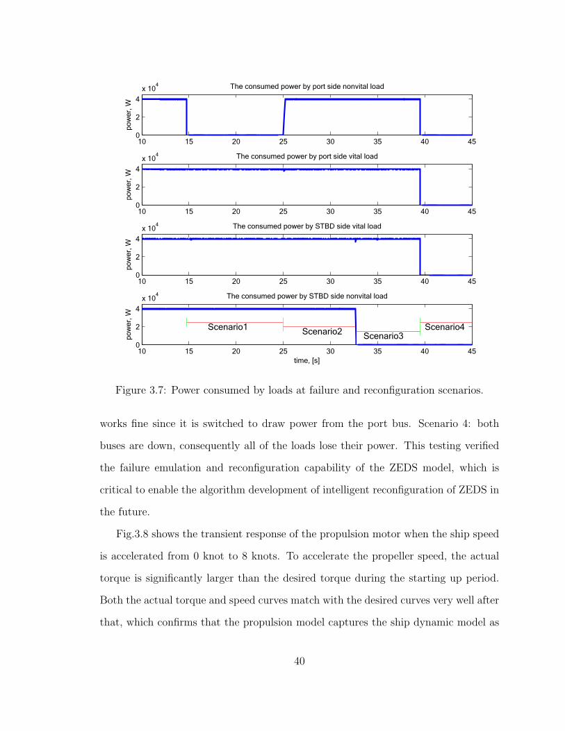
10 15 20 25 30 35 40 450
2
4
x 104 The consumed power by port side nonvital load
pow
er, W
10 15 20 25 30 35 40 450
2
4
x 104
pow
er, W
The consumed power by port side vital load
10 15 20 25 30 35 40 450
2
4
x 104 The consumed power by STBD side vital load
pow
er, W
10 15 20 25 30 35 40 450
2
4
x 104
pow
er, W
The consumed power by STBD side nonvital load
time, [s]
Scenario1 Scenario2 Scenario3Scenario4
Figure 3.7: Power consumed by loads at failure and reconfiguration scenarios.
works fine since it is switched to draw power from the port bus. Scenario 4: both
buses are down, consequently all of the loads lose their power. This testing verified
the failure emulation and reconfiguration capability of the ZEDS model, which is
critical to enable the algorithm development of intelligent reconfiguration of ZEDS in
the future.
Fig.3.8 shows the transient response of the propulsion motor when the ship speed
is accelerated from 0 knot to 8 knots. To accelerate the propeller speed, the actual
torque is significantly larger than the desired torque during the starting up period.
Both the actual torque and speed curves match with the desired curves very well after
that, which confirms that the propulsion model captures the ship dynamic model as
40
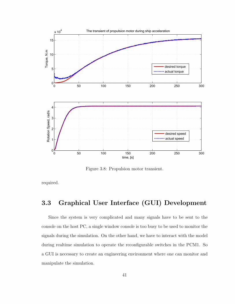
0 50 100 150 200 250 3000
5
10
15
x 104 The transient of propulsion motor during ship accelaration
Tor
que,
N.m
0 50 100 150 200 250 3000
1
2
3
4
Rot
atio
n S
peed
, rad
/s
time, [s]
desired torque
actual torque
desired speed
actual speed
Figure 3.8: Propulsion motor transient.
required.
3.3 Graphical User Interface (GUI) Development
Since the system is very complicated and many signals have to be sent to the
console on the host PC, a single window console is too busy to be used to monitor the
signals during the simulation. On the other hand, we have to interact with the model
during realtime simulation to operate the reconfigurable switches in the PCM1. So
a GUI is necessary to create an engineering environment where one can monitor and
manipulate the simulation.
41
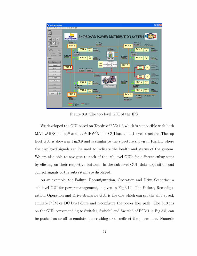
Figure 3.9: The top level GUI of the IPS.
We developed the GUI based on Testdriver V2.1.3 which is compatible with both
MATLAB/Simulinkr and LabVIEWr. The GUI has a multi-level structure. The top
level GUI is shown in Fig.3.9 and is similar to the structure shown in Fig.1.1, where
the displayed signals can be used to indicate the health and status of the system.
We are also able to navigate to each of the sub-level GUIs for different subsystems
by clicking on their respective buttons. In the sub-level GUI, data acquisition and
control signals of the subsystem are displayed.
As an example, the Failure, Reconfiguration, Operation and Drive Scenarios, a
sub-level GUI for power management, is given in Fig.3.10. The Failure, Reconfigu-
ration, Operation and Drive Scenarios GUI is the one which can set the ship speed,
emulate PCM or DC bus failure and reconfigure the power flow path. The buttons
on the GUI, corresponding to Switch1, Switch2 and Switch3 of PCM1 in Fig.3.5, can
be pushed on or off to emulate bus crashing or to redirect the power flow. Numeric
42
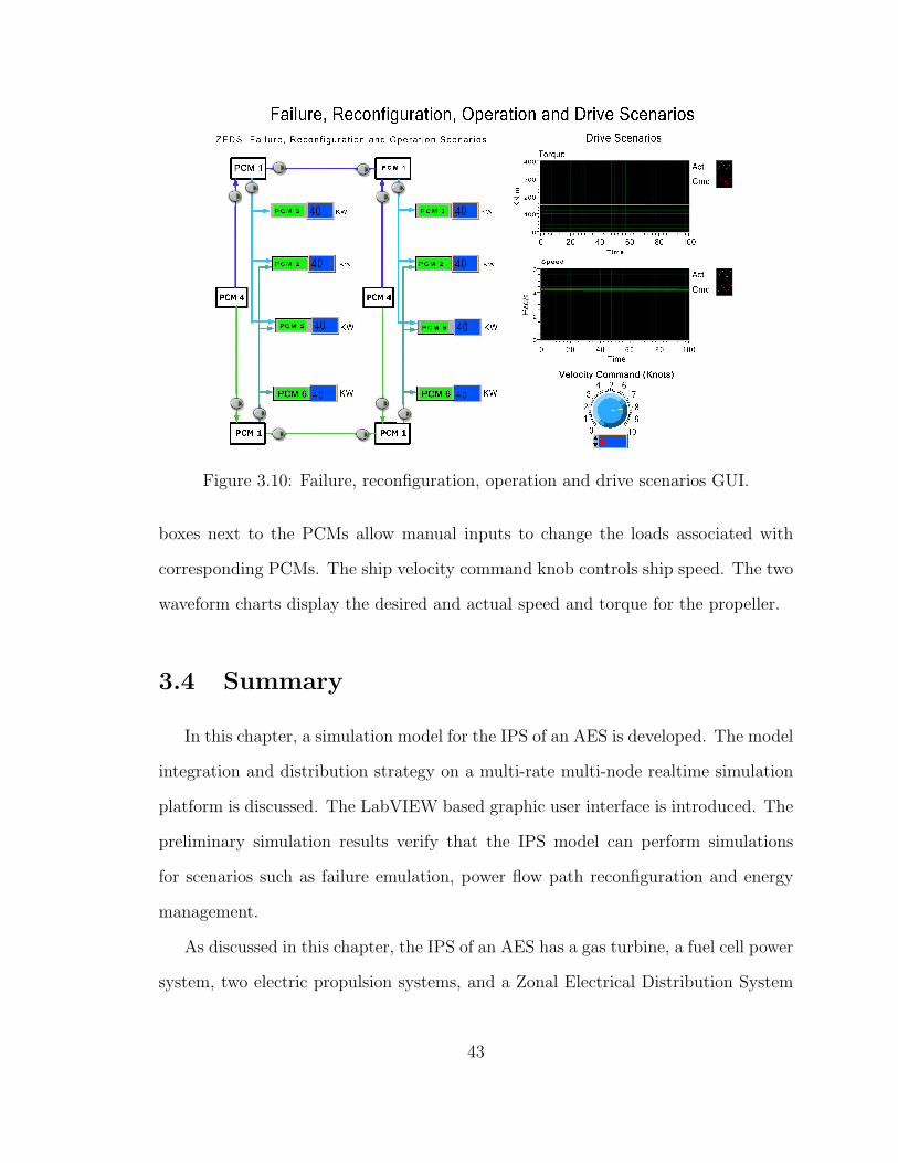
Figure 3.10: Failure, reconfiguration, operation and drive scenarios GUI.
boxes next to the PCMs allow manual inputs to change the loads associated with
corresponding PCMs. The ship velocity command knob controls ship speed. The two
waveform charts display the desired and actual speed and torque for the propeller.
3.4 Summary
In this chapter, a simulation model for the IPS of an AES is developed. The model
integration and distribution strategy on a multi-rate multi-node realtime simulation
platform is discussed. The LabVIEW based graphic user interface is introduced. The
preliminary simulation results verify that the IPS model can perform simulations
for scenarios such as failure emulation, power flow path reconfiguration and energy
management.
As discussed in this chapter, the IPS of an AES has a gas turbine, a fuel cell power
system, two electric propulsion systems, and a Zonal Electrical Distribution System
43

(ZEDS) which, by itself, has many power conversion modules and loads. Both the gas
turbine/generator and the fuel cell power system energize the ZEDS DC bus, forming
an isolated DC Hybrid Power System (DHPS) which has multiple FBCs and a DABC
as the power conditioning devices. However, for the isolated hybrid power system, the
wide range of operating conditions, the requirements for fast power response and load
following, coupled with the stringent constraints of high power quality and system
reliability, have imposed challenges for control of the power converters whose dynamic
characteristics are highly nonlinear. Motivated by the challenges and importance of
the DC Hybrid Power System (DHPS) control, analysis, modeling and control of
power converters for the DHPS will be presented in the following several sections.
44
Chapter 4
Power Flow Characterization of the Dual Active
Bridge Converter
The Dual Active Bridge Converter (DABC) is a bidirectional DC/DC converter
which is used to charge and discharge the energy storage bank of the DHPS. In this
chapter, we will illustrate that the power flow model of a DABC given by [54, 55],
albeit simple, can not be used for effective power flow control design. Therefore, a
novel power flow model for the DABC is developed. The fundamental phenomena
are first introduced. After that, the conventional power flow analysis is introduced.
Then, the effects of minor parameter such as the power semiconductor voltage loss
and dead time are investigated. Based on the analysis, a new power flow model is then
developed. The model can accurately predict the power flow over a wide operating
range. The experimental results confirmed the effectiveness of the new model.
4.1 Fundamental Phenomena of DABCs
Fig.4.1 shows the configuration of the DABC, where Q9 − Q16 are the power
switches, L3 is the leakage inductor of the transformer with turn ratio n3, and Csc and
45
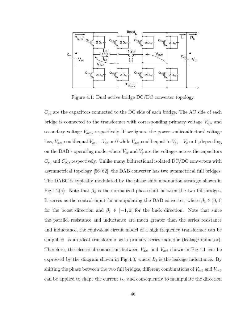
Q9
Q12
3 3Csc Co3
Q11
sc
ac5
Q16
Q15
ac6
o
Q13
Q14
D9 D11
D12
D13
D14
D15
D16
Boost
Buck
65, 5 6
L3
Q10 D10
Figure 4.1: Dual active bridge DC/DC converter topology.
Co3 are the capacitors connected to the DC side of each bridge. The AC side of each
bridge is connected to the transformer with corresponding primary voltage Vac5 and
secondary voltage Vac6, respectively. If we ignore the power semiconductors’ voltage
loss, Vac5 could equal Vsc, −Vsc or 0 while Vac6 could equal to Vo, −Vo or 0, depending
on the DAB’s operating mode, where Vsc and Vo are the voltages across the capacitors
Csc and Co3, respectively. Unlike many bidirectional isolated DC/DC converters with
asymmetrical topology [56–62], the DAB converter has two symmetrical full bridges.
The DABC is typically modulated by the phase shift modulation strategy shown in
Fig.4.2(a). Note that β3 is the normalized phase shift between the two full bridges.
It serves as the control input for manipulating the DAB converter, where β3 ∈ [0, 1]
for the boost direction and β3 ∈ [−1, 0] for the buck direction. Note that since
the parallel resistance and inductance are much greater than the series resistance
and inductance, the equivalent circuit model of a high frequency transformer can be
simplified as an ideal transformer with primary series inductor (leakage inductor).
Therefore, the electrical connection between Vac5 and Vac6 shown in Fig.4.1 can be
expressed by the diagram shown in Fig.4.3, where L3 is the leakage inductance. By
shifting the phase between the two full bridges, different combinations of Vac5 and Vac6
can be applied to shape the current iL3 and consequently to manipulate the direction
46
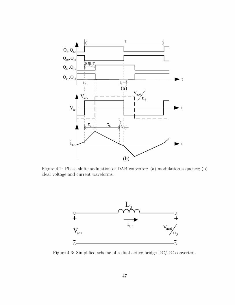
129 Q,Q
5acV
3Li
t
t
t
T
T5.0 3β
3
6acn
V
1110 Q,Q
1613 Q,Q
1514 Q,Q
acV
)b(
aτ bτcτ
0t)a(2T
0t +
Figure 4.2: Phase shift modulation of DAB converter: (a) modulation sequence; (b)ideal voltage and current waveforms.
36acn
V5acV
3Li
3L
Figure 4.3: Simplified scheme of a dual active bridge DC/DC converter .
47
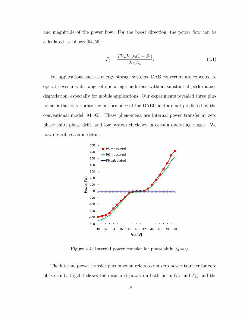
and magnitude of the power flow. For the boost direction, the power flow can be
calculated as follows [54,55]:
P6 =TVscVoβ3(1− β3)
2n3L3
. (4.1)
For applications such as energy storage systems, DAB converters are expected to
operate over a wide range of operating conditions without substantial performance
degradation, especially for mobile applications. Our experiments revealed three phe-
nomena that deteriorate the performance of the DABC and are not predicted by the
conventional model [94, 95]. These phenomena are internal power transfer at zero
phase shift, phase drift, and low system efficiency in certain operating ranges. We
now describe each in detail.
‐500
‐400
‐300
‐200
‐100
0
100
200
300
400
500
600
700
30 32 34 36 38 40 42 44 46 48 50
Power, [W]
Vsc, [V]
P5 measured
P6 measured
P6 calculated
Figure 4.4: Internal power transfer for phase shift β3 = 0.
The internal power transfer phenomenon refers to nonzero power transfer for zero
phase shift. Fig.4.4 shows the measured power on both ports (P5 and P6) and the
48
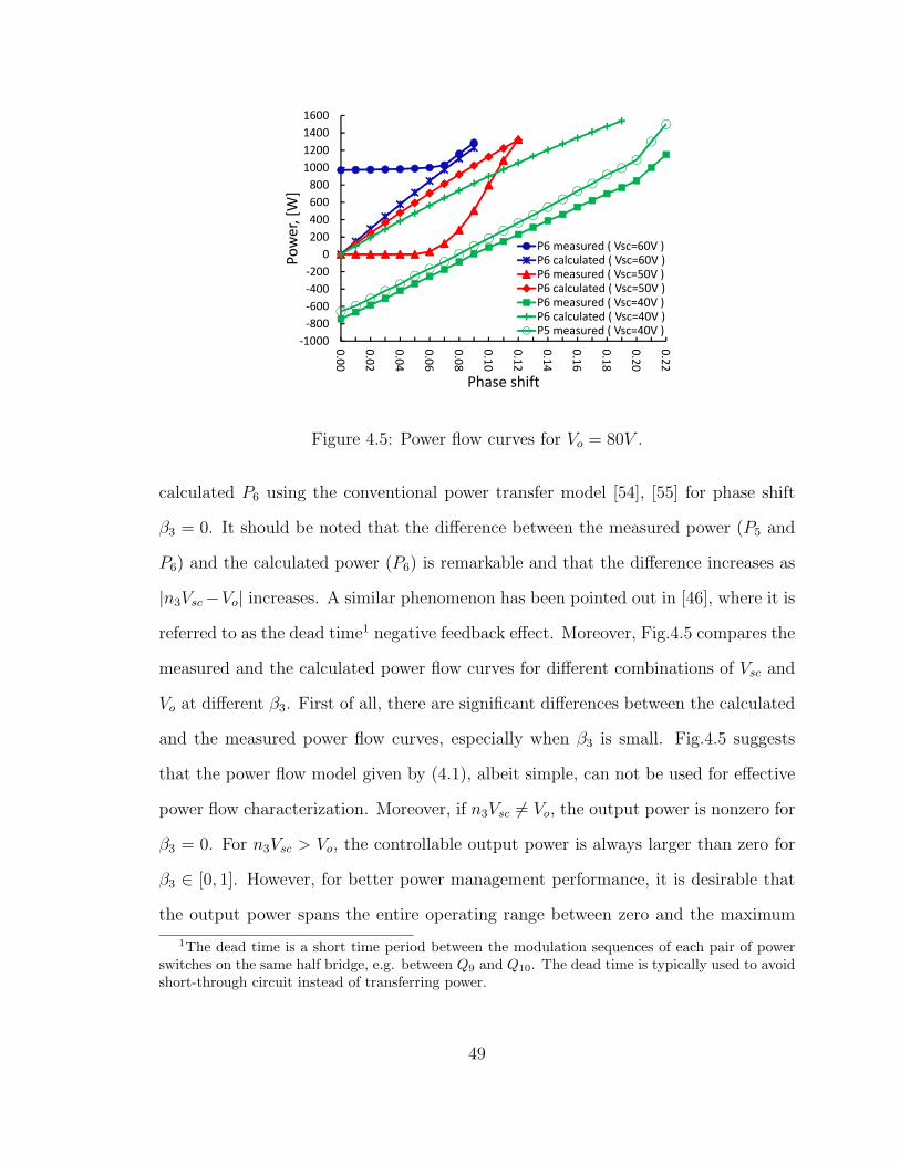
‐1000‐800‐600‐400‐200
02004006008001000120014001600
0.00
0.02
0.04
0.06
0.08
0.10
0.12
0.14
0.16
0.18
0.20
0.22
Power, [W]
Phase shift
P6 measured ( Vsc=60V )P6 calculated ( Vsc=60V )P6 measured ( Vsc=50V )P6 calculated ( Vsc=50V )P6 measured ( Vsc=40V )P6 calculated ( Vsc=40V )P5 measured ( Vsc=40V )
Figure 4.5: Power flow curves for Vo = 80V .
calculated P6 using the conventional power transfer model [54], [55] for phase shift
β3 = 0. It should be noted that the difference between the measured power (P5 and
P6) and the calculated power (P6) is remarkable and that the difference increases as
|n3Vsc−Vo| increases. A similar phenomenon has been pointed out in [46], where it is
referred to as the dead time1 negative feedback effect. Moreover, Fig.4.5 compares the
measured and the calculated power flow curves for different combinations of Vsc and
Vo at different β3. First of all, there are significant differences between the calculated
and the measured power flow curves, especially when β3 is small. Fig.4.5 suggests
that the power flow model given by (4.1), albeit simple, can not be used for effective
power flow characterization. Moreover, if n3Vsc 6= Vo, the output power is nonzero for
β3 = 0. For n3Vsc > Vo, the controllable output power is always larger than zero for
β3 ∈ [0, 1]. However, for better power management performance, it is desirable that
the output power spans the entire operating range between zero and the maximum
1The dead time is a short time period between the modulation sequences of each pair of powerswitches on the same half bridge, e.g. between Q9 and Q10. The dead time is typically used to avoidshort-through circuit instead of transferring power.
49
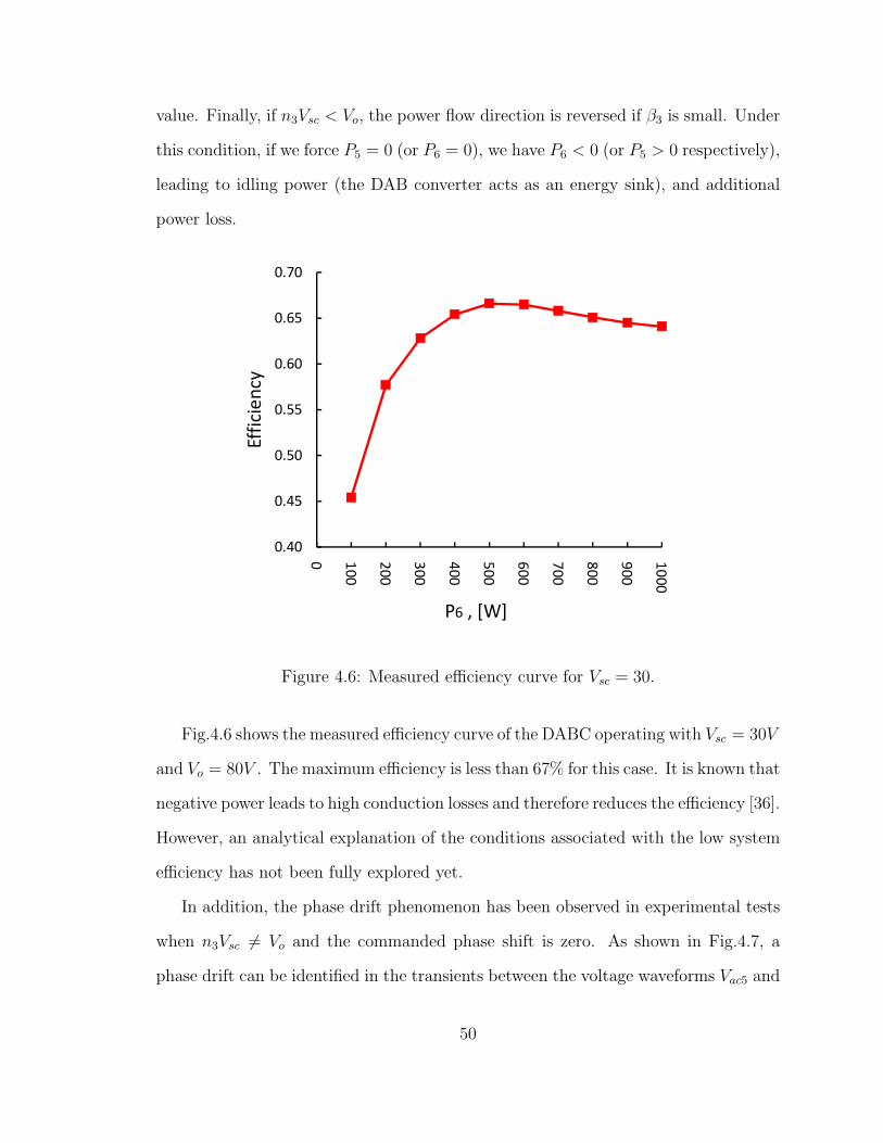
value. Finally, if n3Vsc < Vo, the power flow direction is reversed if β3 is small. Under
this condition, if we force P5 = 0 (or P6 = 0), we have P6 < 0 (or P5 > 0 respectively),
leading to idling power (the DAB converter acts as an energy sink), and additional
power loss.
0.40
0.45
0.50
0.55
0.60
0.65
0.70
0 100
200
300
400
500
600
700
800
900
1000
Efficiency
P6 , [W]
Figure 4.6: Measured efficiency curve for Vsc = 30.
Fig.4.6 shows the measured efficiency curve of the DABC operating with Vsc = 30V
and Vo = 80V . The maximum efficiency is less than 67% for this case. It is known that
negative power leads to high conduction losses and therefore reduces the efficiency [36].
However, an analytical explanation of the conditions associated with the low system
efficiency has not been fully explored yet.
In addition, the phase drift phenomenon has been observed in experimental tests
when n3Vsc 6= Vo and the commanded phase shift is zero. As shown in Fig.4.7, a
phase drift can be identified in the transients between the voltage waveforms Vac5 and
50
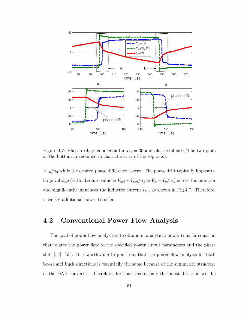
80 90 100 110 120 130 140 150 160 170-50
0
50
time, [μs]
A B
Vac5, [V]
Vac6/n3, [V]
iL3, [A]
95 100 105
-40
-20
0
20
40
time, [μs]
phase drift
A
145 150 155
-40
-20
0
20
40
time, [μs]
phase drift
B
Figure 4.7: Phase drift phenomenon for Vsc = 30 and phase shift= 0 (The two plotsat the bottom are zoomed in characteristics of the top one.).
Vac6/n3 while the desired phase difference is zero. The phase drift typically imposes a
large voltage (with absolute value ' Vac5 +Vac6/n3 ' Vsc+Vo/n3) across the inductor
and significantly influences the inductor current iL3, as shown in Fig.4.7. Therefore,
it causes additional power transfer.
4.2 Conventional Power Flow Analysis
The goal of power flow analysis is to obtain an analytical power transfer equation
that relates the power flow to the specified power circuit parameters and the phase
shift [54], [55]. It is worthwhile to point out that the power flow analysis for both
boost and buck directions is essentially the same because of the symmetric structure
of the DAB converter. Therefore, for conciseness, only the boost direction will be
51

investigated in the subsequent analysis.
Since the dynamics of the capacitor voltages Vsc and Vo are much slower than that
of the inductor current iL3, we can assume that Vsc and Vo are constant over each
switching period. Therefore, to compute the average power, we can define operating
modes according to the evolution of iL3. Whenever the inductor current iL3 either
changes slope or crosses zero, the operating mode changes. Consider the case nVsc <
Vo as an example. For the half switching period [t0, t0 + T2], there are three operating
modes, namely M1, M2 and M3 with corresponding time intervals τa, τb and τc
respectively as illustrated in Fig.4.2(b), where
M1 : t ∈ [t0, t0 + τa];
M2 : t ∈ [t0 + τa, t0 + τa + τb];
M3 : t ∈ [t0 + τa + τb, t0 + T2].
Note that τa+τb+τc = T/2. It is also worthwhile to point out that, for all waveforms
of Vac, iL3, i5 and i6 presented in figures of this dissertation, the time-axis intersects
the y-axis at y = 0.
If we ignore the difference between the input and output power and only consider
the major parameters, namely Vsc, Vo, n3, T and L3, we have:
Vac5 −Vac6n3
= L3diL3
dt=
Vsc + Von3, forM1;
Vsc − Von3, forM2 andM3.
(4.2)
Given the symmetric structure of the DAB converter topology, at steady state,
the average value of iL3(t) must be zero over one switching period T and iL3(t0) =
−iL3(t0 + T2).
52

Therefore,
iL3(t0 +T
2) =
(n3Vsc − Vo)τcn3L3
= −iL3(t0), (4.3)
iL3(t0 + β3T
2) = −(nVsc − Vo)τb
n3L3
=(n3Vsc + Vo)τa
n3L3
+ iL3(t0). (4.4)
(4.3) and (4.4) lead to
(n3Vsc + Vo)τan3L3
+(n3Vsc − Vo)τb
n3L3
− (n3Vsc − Vo)τcn3L3
= 0. (4.5)
Note that,
τa =β3T
2, τa + τb + τc =
T
2. (4.6)
Solving (4.5) and (4.6), we have
τb =(n3Vsc − Vo)− 2n3Vscβ3
2(n3Vsc − Vo)T
2, (4.7)
τc =(n3Vsc − Vo) + 2Voβ3
2(n3Vsc − Vo)T
2. (4.8)
With the assumption that the input and output voltages Vsc and Vo are constant
over one switching period, the average output power P6 can be calculated as:
P6 =2
T
∫ t0+T/2
t0
VsciL3 dt = Vsc ×2
T
∫ t0+T/2
t0
iL3 dt
=2VscT
iL3(t0 + T
2)(τc − τa)
2+iL3(t0 + β3
T2)(τa + τb)
2
=TVscVoβ3(1− β3)
2n3L3
.
(4.9)
Remark 1 At zero phase shift (β3 = 0, τa = β3T2
= 0), we have
53
1. τb = τc = T4
;
2. The slopes of iL3 are the same over the two modes M2 and M32;
3. The average current of iL3 = 2T
∫ t0+T2
t0iL3 dt = 0, therefore P6 = 0.
Note that for n3Vsc ≥ Vo, the power flow expression is the same as (4.9) [54], [55].
Remark 2 We define the power in the desired direction as the positive power and the
power in the opposite direction as the negative power. (4.9) and Remark 7 suggest that,
for zero phase shift, the positive power and the negative power are canceled over the
half switching cycle if we only consider the major parameters. Therefore, the average
output power is always zero. This conclusion contradicts with the experimental results
shown in Fig.4.4, motivating an in-depth power flow analysis for the DAB converter
(to be presented in the subsequent sections).
4.3 Effects of Minor Parameters on Power Trans-
fer of the DABC
Traditional power flow analysis for power converters only considers major param-
eters [65]. This is because most power converters use a dedicated inductor as the
energy transfer element, and the input or output voltage is directly applied to the
inductor. Therefore, the voltage loss of the power semiconductor is negligible. How-
ever, the DAB converter uses a µH or even nH level leakage inductor as the energy
transfer element. The voltage applied to the inductor depends on |Vac5 + Vac6/n3|
and |Vac5 − Vac6/n3| for different time intervals. For many applications [35], [36],
|Vac5 − Vac6/n3| is only several volts, which leads to the hypothesis that the power
2This property holds for all β3 ∈ [0, 1] by (4.2).
54
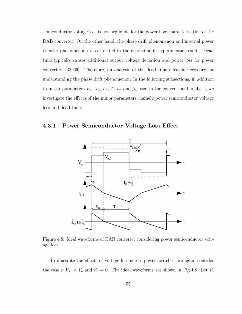
semiconductor voltage loss is not negligible for the power flow characterization of the
DAB converter. On the other hand, the phase drift phenomenon and internal power
transfer phenomenon are correlated to the dead time in experimental results. Dead
time typically causes additional output voltage deviation and power loss for power
converters [32, 66]. Therefore, an analysis of the dead time effect is necessary for
understanding the phase drift phenomenon. In the following subsections, in addition
to major parameters Vsc, Vo, L3, T , n3 and β3 used in the conventional analysis, we
investigate the effects of the minor parameters, namely power semiconductor voltage
loss and dead time.
4.3.1 Power Semiconductor Voltage Loss Effect
5acV
3Li
t
t
nV 6ac
acV
635 in,i t
bτ cτ
T
0t2T
0t +
Figure 4.8: Ideal waveforms of DAB converter considering power semiconductor volt-age loss.
To illustrate the effects of voltage loss across power switches, we again consider
the case n3Vsc < Vo and β3 = 0. The ideal waveforms are shown in Fig.4.8. Let Vs
55

and Vd denote the voltage loss across the power switches Q9 − Q16 and anti-parallel
diodes D9 −D16. Note that, for conciseness, we assume that the power switches and
anti-parallel diodes of the primary full bridge have the same voltage loss as their
corresponding counterparts of the secondary full bridge. In general, the voltage loss
of a power semiconductor may not be constant for varying current. However, for a
given operating range, it is reasonable to assume constant voltage loss because the
conduction resistance of the power semiconductor is very small (mΩ level). We now
proceed to characterize the power flow of the DAB converter as follows:
Define M1, M2 and M3 in the same way as in Section II (now τa = 0 since
β3 = 0), where the voltages across the leakage inductor at different time intervals are
given in Table.4.1:
Table 4.1: Voltage across the leakage inductor considering power semiconductorsvoltage loss
Operating mode Vac5 Vac6M2 Vsc − 2Vs Vo + 2VdM3 Vsc + 2Vd Vo − 2Vs
Given that iL3(t0) = −iL3(t0 + T/2), we have
τbτc
=n3Vsc + 2nVd − (Vo − 2Vs)
n3Vsc − 2nVs − (Vo + 2Vd). (4.10)
(4.10) together with
τa = 0, τa + τb + τc =T
2. (4.11)
will give,
τb =n3Vsc − Vo + 2nVd + 2Vs
2n3Vsc − 2Vo − 2(n− 1)(Vs − Vd)T
2, (4.12)
τc =n3Vsc − Vo − 2nVs − 2Vd
2n3Vsc − 2Vo − 2(n− 1)(Vs − Vd)T
2. (4.13)
56

Moreover,
i5(t) = ni6(t) =
iL3(t), t ∈ [t0, t0 + T2];
−iL3(t), t ∈ [t0 + T2, t0 + T ].
(4.14)
iL3(t0 +T
2) =
(n3Vsc − Vo + 2nVd + 2Vs)τcn3L3
. (4.15)
Therefore, the average power can be calculated as:
P5 =2
T
∫ T/2
0
Vsci5 dt =2VscT
iL3(t0 + T
2)(τc − τb)
2
, (4.16)
P6 =2
T
∫ T/2
0
Voi6 dt =2VoTVsc
∫ T/2
0
Vsci5n3
dt =P5Von3Vsc
. (4.17)
Remark 3 At zero phase shift, the voltage loss of the power semiconductor can cause:
1. τb 6= τc (as shown by (4.10));
2. The slope of iL3 is NOT the same for modes M2 and M3, since the voltage
across the inductor Vac5 − Vac6/n3, calculated using data in Table.4.1, are dif-
ferent;
3. P5 6= 0 and P6 6= 0 as calculated in (4.16), (4.17).
Therefore, the minor parameters Vs and Vd affect the distribution of positive power
and negative power, leading to P5 6= 0 and P6 6= 0 at β3 = 0. Taking this one step
further, the effects of dead time will be considered in the next subsection.
4.3.2 Dead Time Effect
We now show that the existence of a dead time causes the phase drift phenomenon
we noted in the Introduction. For continuity and simplicity, we consider again the
57

case with n3Vsc < Vo and β3 = 0. Referring to the current and voltage waveforms
plotted in Fig.4.9, suppose that the DAB is modulated by gating sequences Vg, with
dead time Td between transits at each half switching period. Given n3Vsc < Vo,
iL3(t) must be decreasing during t0 ≤ t ≤ t0 + T2, since Q9, Q12, Q13 and Q16 are
turned on and Vac5 > 0, Vac6 > 0. Given the symmetric structure of the topology,
iL3(t0) = −iL3(t0 + T2), we must have iL3(t0) > 0 and iL3(t0 + T
2) < 0, implying that
i5 has to pass through D9 and D12 while i6 passes through Q13 and Q16 during τc. At
time t = t0 + T2, Q9, Q12, Q13 and Q16 are turned off, causing i6 to be switched to D14
and D15 immediately while i5 keeps passing through D9 and D12. This is equivalent
to an undesired additional phase shift between Vac5 and Vac6 which enables i5 passing
the power devices Q9/D9 and Q12/D12 during the dead time. We define the undesired
phase shift as phase drift. If iL3(t0 + T2) is not large enough, then iL3(t) will go to
zero before t = t0 + T2
+ Td as shown in Fig.4.9a (Case I), meaning that there is a
negative phase drift ∈ [−2Td/T, 0]. Otherwise, i5 keeps passing through D9 and D12
until the dead time ends and Q10 and Q11 are turned on as shown in Fig.4.9b (Case
II), leading to a negative phase drift −2Td/T . Similarly, for the case n3Vsc > Vo and
d = 0, there is a phase drift (lead) for the primary voltage Vac5 in comparison with
the secondary voltage Vac6.
Remark 4 The phase drift only provides the freewheeling path for the inductor cur-
rent iL3 and iL3 can reach zero but never can cross zero and be built up.
We next derive expressions for the power flow that include the dead time as well
as the voltage loss:
58
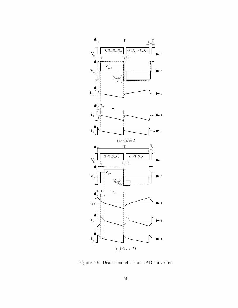
2T
0t +0t
5acV
3Li
t
t
36acn
VacV
5i t
aτcτ
6i t
tgV1613129 Q,Q,Q,Q 15141110 Q,Q,Q,Q
T dT
bτ
(a) Case I
5acV
3Li
t
t
36acn
VacV
5i t
bτ cτ
6i t
tgV8541 ,,, QQQQ 7632 ,,, QQQQ
0t 2T
0t +
T dT
aτ
(b) Case II
Figure 4.9: Dead time effect of DAB converter.
59

Case I
If |Vac5−Vac6/n3| is not large enough to build large |iL3|, then |iL3| reduces to zero
before t = t0 + T2
+ Td, which results in a phase drift ∈ [−2Td/T, 0]. In this case, the
ideal waveforms are shown in Fig.4.9a. Define M1, M2 and M3 in the same way as
in Section II, where the voltages across the leakage inductor at different time intervals
are shown in Table.4.2. Here, M2 is not considered given that iL3 = 0, i5 = 0 and
i6 = 0 for t ∈M2.
Table 4.2: Voltage across the leakage inductor for case I
Operating mode Vac5 Vac6M1 −(Vsc + 2Vd) Vo + 2VdM3 Vsc + 2Vd Vo − 2Vs
From Table.4.2 and
τc =T
2− Td. (4.18)
we can derive,
τa =n3Vsc − Vo + 2n3Vd + 2Vsn3Vsc + Vo + 2(n3 + 1)Vd
τc, (4.19)
iL3(t0 +T
2) =
(n3Vsc − Vo + 2n3Vd + 2Vs)τcn3L3
. (4.20)
Moreover,
i5(t) =
−iL3(t), for t ∈ [t0, t0 + τa];
iL3(t), for t ∈ [t0 + τa, t0 + T/2 + τa];
−iL3(t), for t ∈ [t0 + T/2 + τa, t0 + T ].
(4.21)
60

i6(t) =
iL3(t)n3
, for t ∈ [t0, t0 + T/2];
− iL3(t)n3
, for t ∈ [t0 + T/2, t0 + T ].(4.22)
Therefore, the average powers, P5 and P6, are
P5 =2
T
∫ T/2
0
Vsci5 dt =2VscT
iL3(t0 + T
2)(τa + τc)
2
, (4.23)
P6 =2
T
∫ T/2
0
Voi6 dt =2Von3T
iL3(t0 + T
2)(τc − τa)
2
. (4.24)
Note that, for Case I, |iL3| reduces to zero before t = t0 + T2
+Td. This fact implies
τa + τc ≤ T/2. Therefore, for τb = T/2− τa− τc, there is no power transfer (iL3 = 0).
Case II
If |Vac5−Vac6/n3| is large enough to build large |iL3| such that iL3(t0 + T2
+Td) 6= 0,
then the phase drift equals to −2Td/T . In this case, the ideal waveforms are shown in
Fig.4.9b. Defining M1, M2 and M3 as in Section II, the voltages across the leakage
inductor at different time intervals are shown in Table.4.3.
Table 4.3: Voltage across the leakage inductor for case II
Operating mode Vac5 Vac6M1 −(Vsc + 2Vd) Vo + 2VdM2 Vsc − 2Vs Vo + 2VdM3 Vsc + 2Vd Vo − 2Vs
Given Table.4.3 and
τa = Td, (4.25)
τa + τb + τc =T
2. (4.26)
61

we can derive,
τb =(n3Vsc − Vo + 2n3Vd + 2Vs)
T2
+ 2(Vo + Vd − Vs)Td2n3Vsc − 2Vo − 2(n3 − 1)(Vs − Vd)
, (4.27)
τc =(n3Vsc − Vo − 2Vd − 2n3Vs)
T2− 2n3(Vsc + Vd − Vs)Td
2n3Vsc − 2Vo − 2(n3 − 1)(Vs − Vd). (4.28)
Moreover,
i5(t) =
−iL3(t), for t ∈ [t0, t0 + τa];
iL3(t), for t ∈ [t0 + τa, t0 + T/2 + τa];
−iL3(t), for t ∈ [t0 + T/2 + τa, t0 + T ].
(4.29)
i6(t) =
iL3(t)n3
, for t ∈ [t0, t0 + T/2];
− iL3(t)n3
, for t ∈ [t0 + T/2, t0 + T ].(4.30)
iL3(t0 + Td) =−(n3Vsc − Vo − 2Vd − 2n3Vs)τb
n3L3
, (4.31)
iL3(t0 +T
2) = −iL3(t0) =
(n3Vsc − Vo + 2n3Vd + 2Vs)τcn3L3
. (4.32)
Therefore, the average power P5 and P6 are
P5 =2
T
∫ T/2
0
Vsci5 dt =2VscT
iL3(t0 + T
2)(τa + τc)
2+iL3(t0 + Td)(τb − τa)
2
,
(4.33)
P6 =2
T
∫ T/2
0
Voi6 dt =2Von3T
iL3(t0 + T
2)(τc − τa)
2+iL3(t0 + Td)(τa + τb)
2
. (4.34)
Similarly, for the case of n3Vsc > Vo and β3 = 0, a model for P5 and P6 can be
derived in the same manner. Given the symmetric structure of the DAB converter,
62
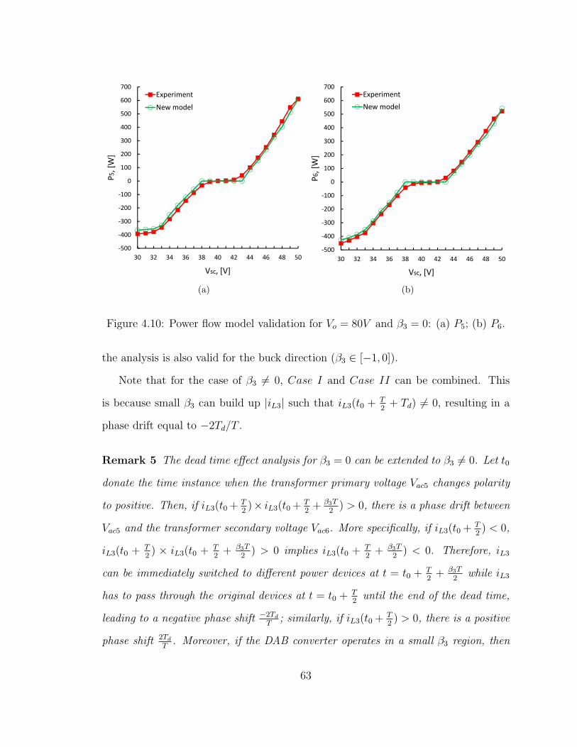
‐500
‐400
‐300
‐200
‐100
0
100
200
300
400
500
600
700
30 32 34 36 38 40 42 44 46 48 50
P5, [W]
Vsc, [V]
Experiment
New model
(a)
‐500
‐400
‐300
‐200
‐100
0
100
200
300
400
500
600
700
30 32 34 36 38 40 42 44 46 48 50
P6, [W]
Vsc, [V]
Experiment
New model
(b)
Figure 4.10: Power flow model validation for Vo = 80V and β3 = 0: (a) P5; (b) P6.
the analysis is also valid for the buck direction (β3 ∈ [−1, 0]).
Note that for the case of β3 6= 0, Case I and Case II can be combined. This
is because small β3 can build up |iL3| such that iL3(t0 + T2
+ Td) 6= 0, resulting in a
phase drift equal to −2Td/T .
Remark 5 The dead time effect analysis for β3 = 0 can be extended to β3 6= 0. Let t0
donate the time instance when the transformer primary voltage Vac5 changes polarity
to positive. Then, if iL3(t0 + T2)× iL3(t0 + T
2+ β3T
2) > 0, there is a phase drift between
Vac5 and the transformer secondary voltage Vac6. More specifically, if iL3(t0 + T2) < 0,
iL3(t0 + T2) × iL3(t0 + T
2+ β3T
2) > 0 implies iL3(t0 + T
2+ β3T
2) < 0. Therefore, iL3
can be immediately switched to different power devices at t = t0 + T2
+ β3T2
while iL3
has to pass through the original devices at t = t0 + T2
until the end of the dead time,
leading to a negative phase shift −2TdT
; similarly, if iL3(t0 + T2) > 0, there is a positive
phase shift 2TdT
. Moreover, if the DAB converter operates in a small β3 region, then
63
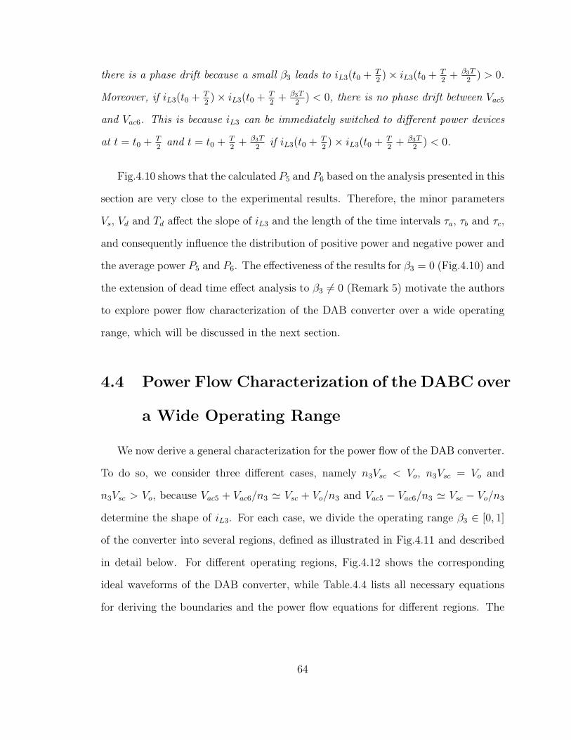
there is a phase drift because a small β3 leads to iL3(t0 + T2)× iL3(t0 + T
2+ β3T
2) > 0.
Moreover, if iL3(t0 + T2)× iL3(t0 + T
2+ β3T
2) < 0, there is no phase drift between Vac5
and Vac6. This is because iL3 can be immediately switched to different power devices
at t = t0 + T2
and t = t0 + T2
+ β3T2
if iL3(t0 + T2)× iL3(t0 + T
2+ β3T
2) < 0.
Fig.4.10 shows that the calculated P5 and P6 based on the analysis presented in this
section are very close to the experimental results. Therefore, the minor parameters
Vs, Vd and Td affect the slope of iL3 and the length of the time intervals τa, τb and τc,
and consequently influence the distribution of positive power and negative power and
the average power P5 and P6. The effectiveness of the results for β3 = 0 (Fig.4.10) and
the extension of dead time effect analysis to β3 6= 0 (Remark 5) motivate the authors
to explore power flow characterization of the DAB converter over a wide operating
range, which will be discussed in the next section.
4.4 Power Flow Characterization of the DABC over
a Wide Operating Range
We now derive a general characterization for the power flow of the DAB converter.
To do so, we consider three different cases, namely n3Vsc < Vo, n3Vsc = Vo and
n3Vsc > Vo, because Vac5 + Vac6/n3 ' Vsc + Vo/n3 and Vac5 − Vac6/n3 ' Vsc − Vo/n3
determine the shape of iL3. For each case, we divide the operating range β3 ∈ [0, 1]
of the converter into several regions, defined as illustrated in Fig.4.11 and described
in detail below. For different operating regions, Fig.4.12 shows the corresponding
ideal waveforms of the DAB converter, while Table.4.4 lists all necessary equations
for deriving the boundaries and the power flow equations for different regions. The
64
following intermediate variables are defined in order to present Table.4.4:
K1 = n3Vsc − Vo + 2n3Vd + 2Vs, (4.35)
K2 = n3Vsc − Vo − 2n3Vs − 2Vd, (4.36)
K3 = 2n3(Vsc + Vd − Vs), (4.37)
K4 = 2(Vo + Vd − Vs), (4.38)
K5 = n3Vsc + Vo − 2(n3 + 1)Vs, (4.39)
K6 = n3Vsc + Vo + 2(n3 + 1)Vd, (4.40)
K7 = 2n3Vsc − 2Vo − 2(n3 − 1)(Vs − Vd), (4.41)
K8 = 2n3Vsc − 2Vo − 2(n3 + 1)(Vs − Vd), (4.42)
i7 = iL3(t0), (4.43)
i8 = iL3(t0 + τa), (4.44)
i9 = iL3(t0 + τa + τb). (4.45)
We now describe each of these regions in detail.
osc3 VVn −1BL2BL3BL
3β
Figure 4.11: Operating region separation.
65

For n3Vsc < Vo, referring to Fig.4.12A/B and Table 4.4 (Region A/B), iL3(t0) > 0
while iL3(t0 + T2) < 0 if the converter operates in a small β3 region. Moreover,
iL3(t0 + T2
+ β3T2
) < 0 for a small β3. Therefore, following Remark 5, there is a
phase drift δ = −2TdT
over a certain range of β3. So, the DAB converter will be
operating with three different regions in this case. The first region (Region A) is
0 ≤ β3 ≤ 2TdT
, wherein β3 +δ is less than zero due to the phase drift. Let BL1, defined
as (Vsc, Vo, β3)|β3 = 2TdT, n3Vsc − Vo ≤ 0, represents the boundary line between
Region A and Region B. In Region B, the phase drift phenomenon still exists, but
the actual phase shift is larger than zero. However, referring to Fig.4.12B and Table
4.4 (Region B), τc decreases as β3 increases. If β3 = −(n3Vsc−Vo−2Vd−2n3Vs)2(Vo+Vd−Vs)
+ 2TdT
,
iL3(t0+ T2) = 0 (τc = 0). Let BL2, defined as (Vsc, Vo, β3)|β3 = −(n3Vsc−Vo−2Vd−2n3Vs)
2(Vo+Vd−Vs)+
2TdT, n3Vsc−Vo ≤ 0, denotes the boundary line between Region B and C, iL3(t0+ T
2) >
0 if the converter operates at the right side of the boundary line BL2. Moreover,
iL3(t0 + T2
+ β3T2
) < 0 in that case, so the current in both bridges can be immediately
switched. Therefore, there is no phase drift, leading to the third region (Region C).
For n3Vsc = Vo, there is a phase drift δ = −2TdT
for small β3 by as discussed
in Remark 5. This is because the DABC works with Discontinuous Current Mode
(DCM) for small β3 such that iL3(t0 + T2) < 0 and iL3(t0 + T
2+ β3T
2) < 0. Moreover,
there is no power transfer if β3 ≤ 2TdT
since iL3(t0 + T2) ' 0 and the phase drift only
provide freewheeling path for iL3 and can not build up inductor current (Remark
4). The DABC operates with Continuous Current Mode (CCM) (iL3(t0 + T2) > 0)
for large β3, and there is no phase drift. Therefore, three regions are defined in this
case. The first region (Region D) is defined by 0 ≤ β3 ≤ 2TdT
, where there is no
power transfer. The DABC operates with DCM mode in the second region (Region
E) wherein δ = −2TdT
. For β3 = (2Vd+2n3Vs)2(Vo+Vd−Vs)
+ 2TdT
, referring to Fig.4.12E and Table
4.4 (Region E), we have iL3(t0 + T2) = 0 (τc = 0). Since n3Vsc = Vo, we can use
66

the same boundary line BL2 to represent the boundary line separating Region E
and F. If the converter operates at the right side of the boundary line BL2, we have
iL3(t0 + β3T2
) > 0 and iL3(t0 + T2
+ β3T2
) < 0, leading to the third region (Region F)
wherein phase drift δ = 0.
For n3Vsc > Vo and small β3, the phase drift is δ = 2TdT
(Remark 5) because
iL3(t0 + T2) > 0 and iL3(t0 + T
2+ β3T
2) > 0. Therefore, two regions are defined in
this case. For the first region (Region G), the actual phase shift equals to β3 + 2TdT
.
If β3 = (n3Vsc−Vo−2Vd−2n3Vs)2n3(Vsc+Vd−Vs)
− 2TdT
, then iL3(t0 + T2
+ β3T2
) = 0 (τb = 0). Let BL3,
defined as (Vsc, Vo, β3)|β3 = (n3Vsc−Vo−2Vd−2n3Vs)2n3(Vsc+Vd−Vs)
− 2TdT, n3Vsc − Vo > 0, representing
the boundary line between Region G and H. If the converter operates at the right
side of the boundary line BL3, we have iL3(t0 + T2) > 0 and iL3(t0 + T
2+ β3T
2) < 0,
leading to the second region (Region H) with zero phase drift.
Note that for all of three cases, namely n3Vsc < Vo, n3Vsc = Vo and n3Vsc > Vo, we
assume that the operating mode of the DAB converter will transfer from the region
with a phase drift (Region B, E or G) to the corresponding one without phase drift
(Region C, F or H) immediately whenever β3 acroses the boundary lines BL2 and
BL3, respectively. But in reality, there will be a short interval wherein the phase
drift phenomenon fades away gradually if β3 acroses the boundary lines. Due to the
symmetric structure of the converter, the analysis can be also applied for the buck
direction operation.
The power flow analysis for different regions can be performed following the same
procedure as presented in Section III. Note that there is no power transfer for Region
D, and Regions F and H have the same power flow characterization as Region C.
Therefore, only waveforms and equations of Region A, B, C, E and G are provided
in Fig.4.12 and Table.4.4.
Remark 6 For different operating regions depicted in Fig.4.11, the influence of the
67
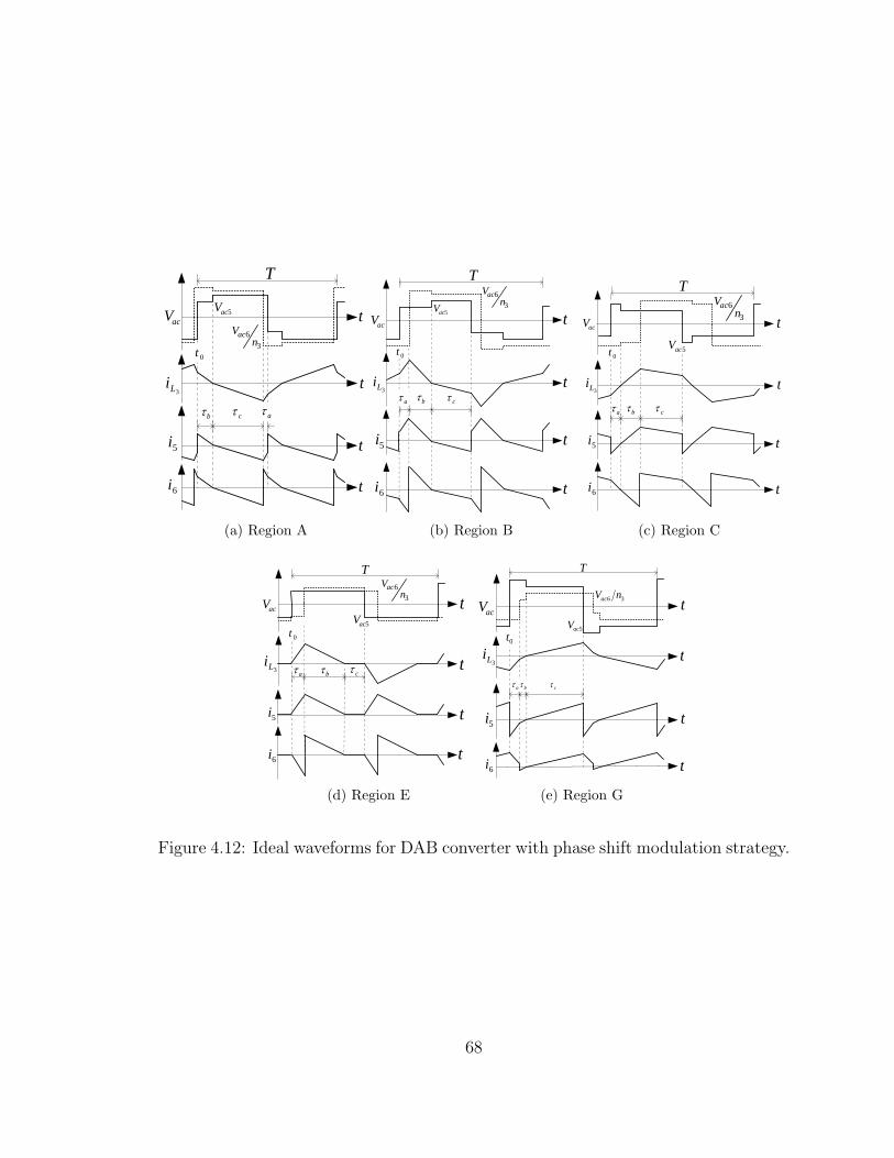
5acV
3Li
t
36
nVac
acV
5i
bτ cτ
6i
t
t
t
T
0t
aτ
(a) Region A
5acV
3Li
t3
6n
Vac
acV
bτ cτ
5i
6i
t
t
t
T
0t
aτ
(b) Region B
5acV
3Li
t
t
36n
Vac
acV
t
aτ bτ cτ
t
5i
6i
0t
T
(c) Region C
5acV
3Li
t
t
36
nVac
acV
t
aτ bτ
t
5i
6i
T
0t
cτ
(d) Region E
5acV
3Li
t
t
acV36 nVac
5i t
aτ cτ
t6i
T
0t
bτ
(e) Region G
Figure 4.12: Ideal waveforms for DAB converter with phase shift modulation strategy.
68
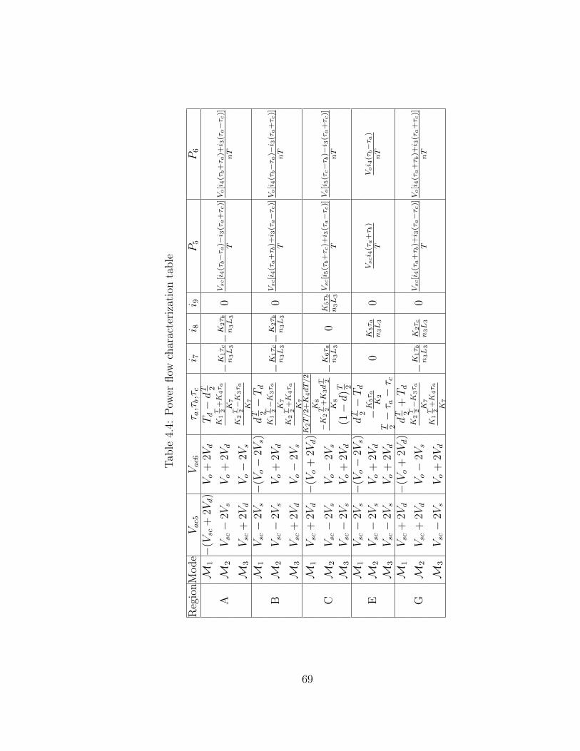
Tab
le4.
4:P
ower
flow
char
acte
riza
tion
table
Reg
ion
Mode
Vac5
Vac6
τ a,τb,τc
i 7i 8
i 9P
5P
6
M1−
(Vsc
+2V
d)Vo
+2V
dTd−dT 2
AM
2Vsc−
2Vs
Vo
+2V
dK
1T 2
+K
4τ a
K7
−K
1τ c
n3L
3−K
2τ b
n3L
30
Vsc[i
4(τb−τ a
)−i 3
(τa+τ c
)]T
Vo[i
4(τb+τ a
)+i 3
(τa−τ c
)]nT
M3
Vsc
+2V
dVo−
2Vs
K2T 2−K
3τ a
K7
M1
Vsc−
2Vs−
(Vo−
2Vs)
dT 2−Td
BM
2Vsc−
2Vs
Vo
+2V
dK
1T 2−K
3τ a
K7
−K
1τ c
n3L
3−K
2τ b
n3L
30
Vsc[i
4(τa+τ b
)+i 3
(τa−τ c
)]T
Vo[i
4(τb−τ a
)−i 3
(τa+τ c
)]nT
M3
Vsc
+2V
dVo−
2Vs
K2T 2
+K
4τ a
K7
M1
Vsc
+2V
d−
(Vo
+2V
d)K
2T/2+K
4dT/2
K8
CM
2Vsc−
2Vs
Vo−
2Vs
−K
2T 2
+K
3dT 2
K8
−K
6τ a
n3L
30
K5τ b
n3L
3
Vsc[i
5(τb+τ c
)+i 3
(τa−τ c
)]T
Vo[i
5(τc−τ b
)−i 3
(τa+τ c
)]nT
M3
Vsc−
2Vs
Vo
+2V
d(1−d)T
2
M1
Vsc−
2Vs−
(Vo−
2Vs)
dT 2−Td
EM
2Vsc−
2Vs
Vo
+2V
d−K
5τ a
K2
0K
5τ a
n3L
30
Vsci 4
(τa+τ b
)T
Voi 4
(τb−τ a
)nT
M3
Vsc−
2Vs
Vo
+2V
dT 2−τ a−τ c
M1
Vsc
+2V
d−
(Vo
+2V
d)
dT 2
+Td
GM
2Vsc
+2V
dVo−
2Vs
K2T 2−K
3τ a
K7
−K
1τ b
n3L
3
K2τ c
n3L
30
Vsc[i
4(τa+τ b
)+i 3
(τa−τ c
)]T
Vo[i
4(τa+τ b
)+i 3
(τa+τ c
)]nT
M3
Vsc−
2Vs
Vo
+2V
dK
1T 2
+K
4τ a
K7
69

minor parameters on operating regions are summarized as follows:
1. Dead time introduces negative phase drift in Regions A, B, D and E and positive
phase drift in Region G. Dead time has no impact in Regions C, F and H.
Moreover, in Regions A, B, and G, the converter operates with hard switching
since it does not satisfy the soft-switching condition given by [54]. In addition,
phase drift introduces additional negative power over each half switching period
in Regions A, B, and G, leading to high conduction loss. Furthermore, for high
power applications, since the dead time has to be chosen large enough to assure
safe operation of the converter, the dead time effect will be significant if the
converter operates in Region A, B and G. Therefore, the DAB converter should
be designed such that the nominal operation point is outside Region A, B and
G to achieve high system efficiency.
2. For all operating regions, the voltage loss of power devices affects the slope of
iL3 and the distribution of positive power and negative power, and consequently
influence the average power P5 and P6. Moreover, the voltage drop effect is more
prominent for low voltage applications than that for high voltage applications,
where an external inductor is often used as the energy transfer element and high
voltage will be applied to the inductor in latter case.
Fig.4.13 shows the power curves of the conventional model and the new model for
Vsc = 30V , Vo = 80V , Vs = 2V , Vd = 1V and β3 ∈ [0, 1]. If the minor parameters are
nonzero, from the power flow curves calculated by the new model, if 0 ≤ β3 < 0.078,
then P5 < 0 and P6 < 0, indicating that the power flow direction is opposite to the
desired direction (Reversed Power Flow). For 0.078 ≤ β3 < 0.088 or 0.96 ≤ β3 ≤
1, P5 > 0 and P6 < 0, the DAB converter acts as an energy sink (Energy Sink),
meaning that the converter draws power from both the P5 and P6 ports and the
70
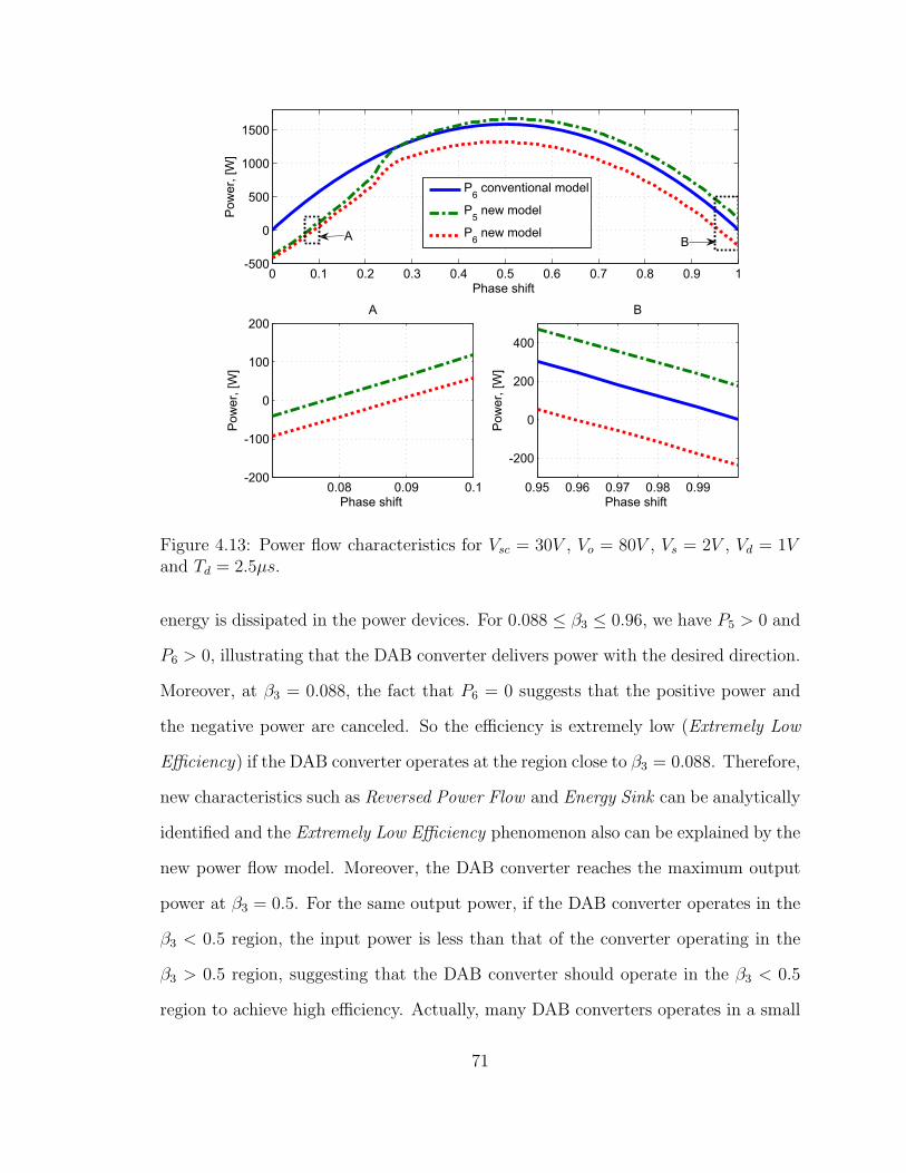
0 0.1 0.2 0.3 0.4 0.5 0.6 0.7 0.8 0.9 1-500
0
500
1000
1500
Phase shift
Pow
er, [
W]
0.08 0.09 0.1-200
-100
0
100
200
Phase shift
Pow
er, [
W]
A
0.95 0.96 0.97 0.98 0.99
-200
0
200
400
Phase shift P
ower
, [W
]
B
P6 conventional model
P5 new model
P6 new modelA B
Figure 4.13: Power flow characteristics for Vsc = 30V , Vo = 80V , Vs = 2V , Vd = 1Vand Td = 2.5µs.
energy is dissipated in the power devices. For 0.088 ≤ β3 ≤ 0.96, we have P5 > 0 and
P6 > 0, illustrating that the DAB converter delivers power with the desired direction.
Moreover, at β3 = 0.088, the fact that P6 = 0 suggests that the positive power and
the negative power are canceled. So the efficiency is extremely low (Extremely Low
Efficiency) if the DAB converter operates at the region close to β3 = 0.088. Therefore,
new characteristics such as Reversed Power Flow and Energy Sink can be analytically
identified and the Extremely Low Efficiency phenomenon also can be explained by the
new power flow model. Moreover, the DAB converter reaches the maximum output
power at β3 = 0.5. For the same output power, if the DAB converter operates in the
β3 < 0.5 region, the input power is less than that of the converter operating in the
β3 > 0.5 region, suggesting that the DAB converter should operate in the β3 < 0.5
region to achieve high efficiency. Actually, many DAB converters operates in a small
71
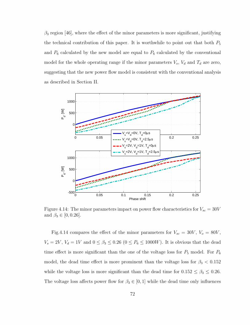
β3 region [46], where the effect of the minor parameters is more significant, justifying
the technical contribution of this paper. It is worthwhile to point out that both P5
and P6 calculated by the new model are equal to P6 calculated by the conventional
model for the whole operating range if the minor parameters Vs, Vd and Td are zero,
suggesting that the new power flow model is consistent with the conventional analysis
as described in Section II.
0 0.05 0.1 0.15 0.2 0.25
0
500
1000
P 5, [W
]
0 0.05 0.1 0.15 0.2 0.25-500
0
500
1000
Phase shift
P 6, [W
]
Vs=V
d=0V, T
d=0μs
Vs=V
d=0V, T
d=2.5μs
Vs=2V, V
d=1V, T
d=0μs
Vs=2V, V
d=1V, T
d=2.5μs
Figure 4.14: The minor parameters impact on power flow characteristics for Vsc = 30Vand β3 ∈ [0, 0.26].
Fig.4.14 compares the effect of the minor parameters for Vsc = 30V , Vo = 80V ,
Vs = 2V , Vd = 1V and 0 ≤ β3 ≤ 0.26 (0 ≤ P6 ≤ 1000W ). It is obvious that the dead
time effect is more significant than the one of the voltage loss for P5 model. For P6
model, the dead time effect is more prominent than the voltage loss for β3 < 0.152
while the voltage loss is more significant than the dead time for 0.152 ≤ β3 ≤ 0.26.
The voltage loss affects power flow for β3 ∈ [0, 1] while the dead time only influences
72
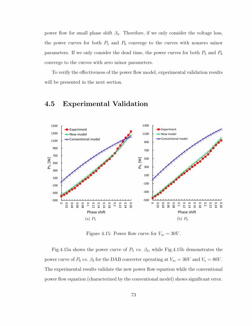
power flow for small phase shift β3. Therefore, if we only consider the voltage loss,
the power curves for both P5 and P6 converge to the curves with nonzero minor
parameters. If we only consider the dead time, the power curves for both P5 and P6
converge to the curves with zero minor parameters.
To verify the effectiveness of the power flow model, experimental validation results
will be presented in the next section.
4.5 Experimental Validation
‐500
‐300
‐100
100
300
500
700
900
1100
1300
1500
0 0.02
0.04
0.06
0.08
0.1
0.12
0.14
0.16
0.18
0.2
0.22
0.24
0.26
P5, [W]
Phase shift
ExperimentNew modelConventional model
(a) P5
‐500
‐300
‐100
100
300
500
700
900
1100
1300
0 0.02
0.04
0.06
0.08
0.1
0.12
0.14
0.16
0.18
0.2
0.22
0.24
0.26
P6, [W]
Phase shift
Experiment
New model
Conventional model
(b) P6
Figure 4.15: Power flow curve for Vsc = 30V .
Fig.4.15a shows the power curve of P5 vs. β3, while Fig.4.15b demonstrates the
power curve of P6 vs. β3 for the DAB converter operating at Vsc = 30V and Vo = 80V .
The experimental results validate the new power flow equation while the conventional
power flow equation (characterized by the conventional model) shows significant error.
73
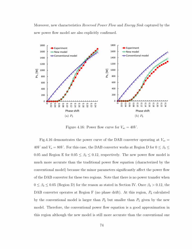
Moreover, new characteristics Reversed Power Flow and Energy Sink captured by the
new power flow model are also explicitly confirmed.
0
200
400
600
800
1000
1200
1400
1600
1800
0 0.02
0.04
0.06
0.08
0.10
0.12
0.14
0.16
0.18
0.20
0.22
0.24
P5, [W]
Phase shift
ExperimentNew modelConventional model
(a) P5
0
200
400
600
800
1000
1200
1400
1600
1800
0 0.02
0.04
0.06
0.08
0.10
0.12
0.14
0.16
0.18
0.20
0.22
0.24
P6, [W]
Phase shift
ExperimentNew modelConventional model
(b) P6
Figure 4.16: Power flow curve for Vsc = 40V .
Fig.4.16 demonstrates the power curve of the DAB converter operating at Vsc =
40V and Vo = 80V . For this case, the DAB converter works at Region D for 0 ≤ β3 ≤
0.05 and Region E for 0.05 ≤ β3 ≤ 0.12, respectively. The new power flow model is
much more accurate than the traditional power flow equation (characterized by the
conventional model) because the minor parameters significantly affect the power flow
of the DAB converter for these two regions. Note that there is no power transfer when
0 ≤ β3 ≤ 0.05 (Region D) for the reason as stated in Section IV. Once β3 > 0.12, the
DAB converter operates at Region F (no phase drift). At this region, P6 calculated
by the conventional model is larger than P6 but smaller than P5 given by the new
model. Therefore, the conventional power flow equation is a good approximation in
this region although the new model is still more accurate than the conventional one
74
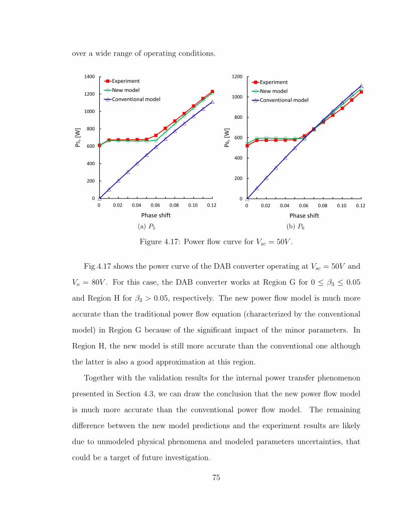
over a wide range of operating conditions.
0
200
400
600
800
1000
1200
1400
0 0.02 0.04 0.06 0.08 0.10 0.12
P5, [W]
Phase shift
Experiment
New model
Conventional model
(a) P5
0
200
400
600
800
1000
1200
0 0.02 0.04 0.06 0.08 0.10 0.12
P6, [W]
Phase shift
Experiment
New model
Conventional model
(b) P6
Figure 4.17: Power flow curve for Vsc = 50V .
Fig.4.17 shows the power curve of the DAB converter operating at Vsc = 50V and
Vo = 80V . For this case, the DAB converter works at Region G for 0 ≤ β3 ≤ 0.05
and Region H for β3 > 0.05, respectively. The new power flow model is much more
accurate than the traditional power flow equation (characterized by the conventional
model) in Region G because of the significant impact of the minor parameters. In
Region H, the new model is still more accurate than the conventional one although
the latter is also a good approximation at this region.
Together with the validation results for the internal power transfer phenomenon
presented in Section 4.3, we can draw the conclusion that the new power flow model
is much more accurate than the conventional power flow model. The remaining
difference between the new model predictions and the experiment results are likely
due to unmodeled physical phenomena and modeled parameters uncertainties, that
could be a target of future investigation.
75

4.6 Summary
This chapter presents a new power flow model for a DABC over a wide operating
range based on in-depth short time scale process analysis. In addition to those major
parameters used by conventional power flow analysis, this new model incorporates
minor parameters, namely the power semiconductor voltage loss and dead time. The
minor parameters are shown to be critical in explaining the observed phenomena,
which are relevant to power flow characterization of the DAB converter. Therefore,
the new model can serve as a research tool for optimal hardware design, operating
range selection and power management strategy development. The experimental
results illustrate the effectiveness of the new model.
In the process of developing the more accurate power flow characterization for the
DABC, we identified the performance limitations of the converter for energy storage
applications. It was also recognized that such limitations are due to the drawbacks
of the modulation strategy. The subsequent effort in developing a new modulation
strategy to overcome the limitations has led to a novel CM-PWM strategy described
in the next Chapter.
76

Chapter 5
Development of a Current-Mode PWM Strategy
for the Dual Active Bridge Converter
The new model developed in Chapter 4 provides more insight on the operation of
the DABC and leads to the development of a Current-Mode PWM (CM-PWM) strat-
egy proposed in this chapter. The new modulation strategy overcomes the drawbacks
of the PSM strategy and improves the performance of the DABC for energy storage
applications. The characteristics of the new strategy are analyzed, followed by ex-
perimental results that confirm the superior performance of the dual active converter
modulated by the proposed new modulation strategy.
5.1 CM-PWM Strategy
To overcome the drawbacks of the DAB converter modulated by PSM, we propose
the CM-PWM to achieve several goals, namely zero circulating current, soft-switching
over a wide operating range, zero idling power, simple but accurate power flow char-
acterization, and high power density but low component stress. Note that, given the
symmetric structure of the DAB converter, the analysis and derivation are essentially
77

the same for both the boost and the buck direction. For conciseness, we only present
the analysis and derivation for the boost direction. We now describe the CM-PWM
in detail.
The modulation mechanism is demonstrated in Fig.5.1(a) while the ideal wave-
forms are shown in Fig.5.1(b). We define β3 ∈ [0, 1] as the pulse width of the inductor
current, and α1β3 and α2β3 as the duty ratios for Vac5 and Vac6, respectively. Note
that since the voltage drops on the power semiconductor are relatively small in com-
parison with Vsc and Vo, Vac5 ' Vsc and Vac6 ' Vo. To achieve zero current at both
t = t0 and t = t0 + β3T2
= t3, by the voltage-second balance equation for the inductor,
it is easy to derive that
α1 = mα2. (5.1)
where
m =Von3Vsc
. (5.2)
Given the ideal waveforms shown in Fig.5.1(b), we have
i5(t) =
iL3(t), t ∈ [t0, t2];
0, t ∈ [t2, t4].(5.3)
i6(t) =
0, t ∈ [t0, t1];
iL3(t)n3
, t ∈ [t1, t3];
0, t ∈ [t3, t4].
(5.4)
By enforcing the pulse width constraint (7.2), we have iL3(t0) = 0 and iL3(t3) = 0.
Therefore, Zero Current Switching (ZCS) at t = t0 and t = t3 are achieved. Moreover,
78
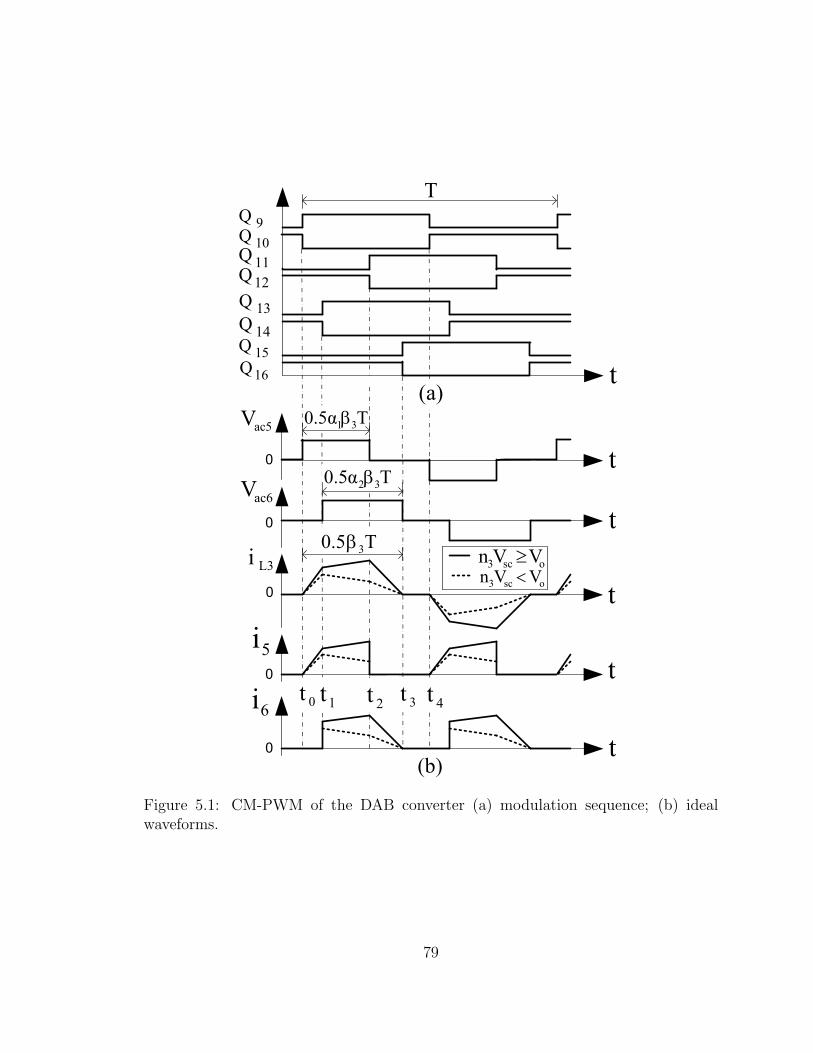
tT0.5α 31β
T0.5α 32β
ac5V
L3i
5i
6i
T
ac6V
9Q10Q11Q12Q
14Q15Q16Q
T0.5 3β
0t 1t 3t2t 4t
0
0
0
0
0
(a)
(b)
t
t
t
t
t
13Q
osc3 VVn ≥osc3 VVn <
Figure 5.1: CM-PWM of the DAB converter (a) modulation sequence; (b) idealwaveforms.
79
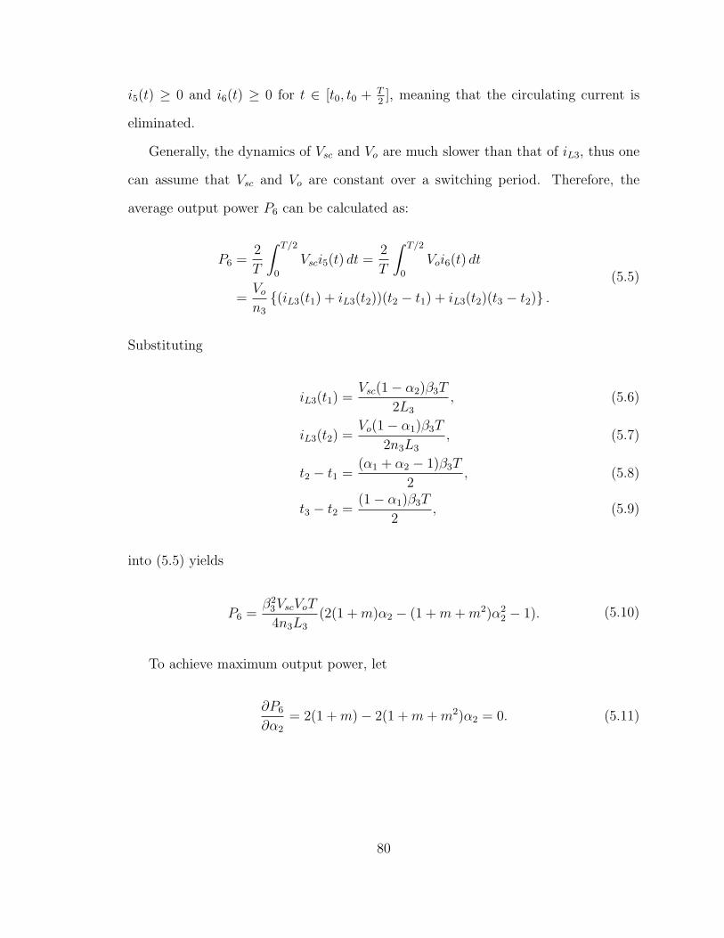
i5(t) ≥ 0 and i6(t) ≥ 0 for t ∈ [t0, t0 + T2], meaning that the circulating current is
eliminated.
Generally, the dynamics of Vsc and Vo are much slower than that of iL3, thus one
can assume that Vsc and Vo are constant over a switching period. Therefore, the
average output power P6 can be calculated as:
P6 =2
T
∫ T/2
0
Vsci5(t) dt =2
T
∫ T/2
0
Voi6(t) dt
=Von3
(iL3(t1) + iL3(t2))(t2 − t1) + iL3(t2)(t3 − t2) .(5.5)
Substituting
iL3(t1) =Vsc(1− α2)β3T
2L3
, (5.6)
iL3(t2) =Vo(1− α1)β3T
2n3L3
, (5.7)
t2 − t1 =(α1 + α2 − 1)β3T
2, (5.8)
t3 − t2 =(1− α1)β3T
2, (5.9)
into (5.5) yields
P6 =β2
3VscVoT
4n3L3
(2(1 +m)α2 − (1 +m+m2)α22 − 1). (5.10)
To achieve maximum output power, let
∂P6
∂α2
= 2(1 +m)− 2(1 +m+m2)α2 = 0. (5.11)
80
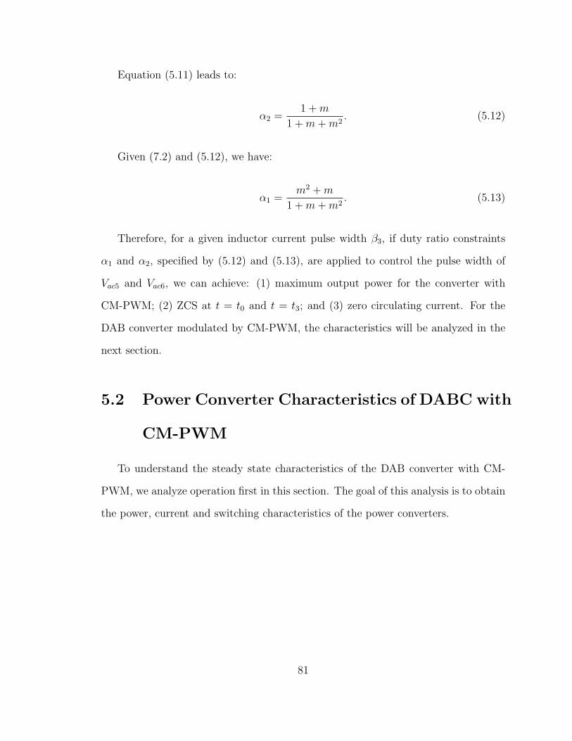
Equation (5.11) leads to:
α2 =1 +m
1 +m+m2. (5.12)
Given (7.2) and (5.12), we have:
α1 =m2 +m
1 +m+m2. (5.13)
Therefore, for a given inductor current pulse width β3, if duty ratio constraints
α1 and α2, specified by (5.12) and (5.13), are applied to control the pulse width of
Vac5 and Vac6, we can achieve: (1) maximum output power for the converter with
CM-PWM; (2) ZCS at t = t0 and t = t3; and (3) zero circulating current. For the
DAB converter modulated by CM-PWM, the characteristics will be analyzed in the
next section.
5.2 Power Converter Characteristics of DABC with
CM-PWM
To understand the steady state characteristics of the DAB converter with CM-
PWM, we analyze operation first in this section. The goal of this analysis is to obtain
the power, current and switching characteristics of the power converters.
81

5.2.1 Power Flow Calculation
For the DAB converter modulated by the CM-PWM, the output power can be
calculated by substituting (5.12) into (5.10) as:
P6 =β2
3V2scV
2o T
4L3(n23V
2sc + n3VscVo + V 2
o ). (5.14)
Therefore, zero idling power is achievable by enforcing β3 = 0. Given (6.4), the
maximum output power can be derived as
P6max =V 2scV
2o T
4L3(n23V
2sc + n3VscVo + V 2
o ). (5.15)
If the DAB converter is modulated by PSM, the output power [54] is:
P ′6 =TVscVoβ3(1− β3)
2n3L′3. (5.16)
The maximum output power is:
P ′6max =TVscVo8n3L′3
. (5.17)
Moreover, with the same inductor (L3 = L′3),
P6max
P ′6max=
2n3VscVon2
3V2sc + n3VscVo + V 2
o
≤ 2
3. (5.18)
This suggests that, with the same inductor, the maximum output power of the DAB
converter modulated by CM-PWM is less than that of the converter modulated by
PSM.
82

5.2.2 Current Stress
Given the inductor current shape shown in Fig.5.1, if the DAB converter is mod-
ulated with CM-PWM, the inductor peak current ipk can be calculated as:
ipk =
iL3(t1) = Vsc(1−α2)β3T
2L, for n3Vsc ≤ Vo;
iL3(t2) = Vo(1−α1)β3T2nL
, for n3Vsc > Vo.
(5.19)
By (5.19), when β3 = 1, the DAB converter with CM-PWM delivers maximum
output power for given Vsc and Vo. Under this condition, the maximum peak current
ipkmax is:
ipkmax =
iL3(t1) = Vsc(1−α2)T
2L3, for n3Vsc ≤ Vo;
iL3(t2) = Vo(1−α1)T2n3L3
, for n3Vsc > Vo.
(5.20)
For the DAB converter modulated with PSM, the inductor peak current is:
i′pk =
iL3(t1) = T (Vo−n3Vsc+2n3Vscβ)
4n3L′3, for n3Vsc ≤ Vo;
iL3(t2) = T (n3Vsc−Vo+2Voβ)4n3L′3
, for n3Vsc > Vo.
(5.21)
According to (5.16), if β3 = 0.5, the DAB converter delivers maximum output power
which introduces the maximum peak current:
i′pkmax =
iL3(t1) = TVo
4n3L′3, for n3Vsc ≤ Vo;
iL3(t2) = Tn3Vsc4n3L′3
, for n3Vsc > Vo.
(5.22)
83

If we choose
L3 =2n3VscVoL
′3
n23V
2sc + n3VscVo + V 2
o
< L′3. (5.23)
Then ipkmax = i′pkmax and P6max = P ′6max. Therefore, the power density of a DAB
converter with CW-PWM can be designed the same as that of a DAB converter with
PSM under the same component stress.
5.2.3 Soft-Switching Range
It is known that the switching loss will be minimized if the power converter op-
erates with soft switching commutation. Therefore, it is desirable to understand the
switching characteristics of the DAB converter with CM-PWM. Referring to Fig.5.1,
using an analysis method similar to that presented in [46], the switching characteris-
tics of the CM-PWM modulated DAB converter can be analyzed as follows:
1. t = t0 : Q10 turns off and Q9 turns on. Since iL3(t0) = 0, Q10 is ZCS OFF while
Q9 is ZCS ON. After this transition, in B1, iL3 passes through Q9 and Q12 while
in B2, iL3 passes through Q14 and D16.
2. t = t1 : Q6 turns off and Q5 turns on. Since iL3(t0) > 0, Q6 is ZVS OFF while
Q13 is ZVS ON. After this transition, in B1, iL3 passes through Q9 and Q12
while in B2, iL3 passes through D13 and D16.
3. t = t2 : Q12 turns off and Q11 turns on. Since iL3(t0) > 0, Q12 is ZVS OFF
while Q11 is ZVS ON. After this transition, in B1, iL3 passes through Q9 and
D11 while in B2, iL3 passes through D13 and D16.
4. t = t3 : Q16 turns off and Q7 turns on. Since iL3(t0) = 0, Q16 is ZCS OFF while
Q7 is ZCS ON. After this transition, Q9 and Q11 in B1 are on while Q13 and
84

Q15 in B2 are on.
Therefore, ZCS/ZVS over the first half switching period is achieved. Similarly,
ZCS/ZVS is also achievable over the second half switching period (t ∈ [t4, t4 + T2]).
Remark 7 Combining the conclusion from the previous section, we can summarize
the following features achieved by the CM-PWM strategy:
1. zero circulating current that reduces conduction loss;
2. ZCS/ZVS over a wide operating range to minimize switching loss;
3. zero idling power to eliminate idle loss;
4. simple power flow characterization;
5. the same power density under the same current stress as the DAB converter
with PSM.
Therefore, the proposed CM-PWM strategy can improve the performance of the DAB
converter over a wide operating range without compromising power density.
5.3 Experimental Validation
Fig.5.2 shows the experimental waveforms of the DAB converter with CM-PWM
for Vsc = 40V , Vo = 100V and β3 = 0.8. The inductor current increases from zero
to its maximum and then decreases to zero at the end of β3T2
. This confirms that
ZCS/ZVS is achieved.
Fig.5.3 compares the calculated power flow curves using (6.4) and the measured
power flow curves of the DAB converter with CM-PWM. The calculated curves match
the measured curves very well, indicating the accuracy of the simple power flow equa-
tion (6.4) and the controllability of the output power between zero and its maximum.
85
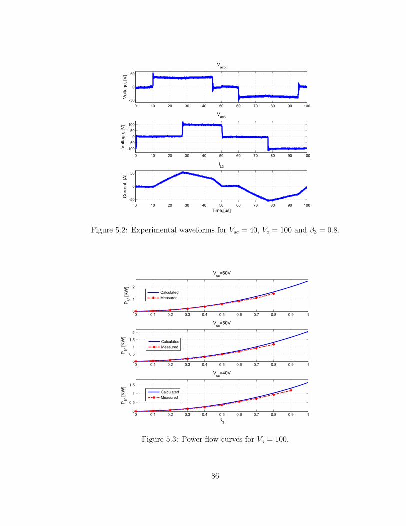
0 10 20 30 40 50 60 70 80 90 100-50
0
50
Vac5
Vol
tage
, [V
]
0 10 20 30 40 50 60 70 80 90 100
-100-50
050
100
Vac6
Vol
tage
, [V
]
0 10 20 30 40 50 60 70 80 90 100-50
0
50
iL3
Cur
rent
, [A
]
Time,[us]
Figure 5.2: Experimental waveforms for Vsc = 40, Vo = 100 and β3 = 0.8.
0 0.1 0.2 0.3 0.4 0.5 0.6 0.7 0.8 0.9 10
1
2
P 6, [K
W]
Vsc
=60V
CalculatedMeasured
0 0.1 0.2 0.3 0.4 0.5 0.6 0.7 0.8 0.9 10
0.5
1
1.5
2
P 6, [K
W]
Vsc
=50V
CalculatedMeasured
0 0.1 0.2 0.3 0.4 0.5 0.6 0.7 0.8 0.9 10
0.5
1
1.5
P 6, [K
W]
Vsc
=40V
β3
CalculatedMeasured
Figure 5.3: Power flow curves for Vo = 100.
86
Moreover, P5 = P6 = 0 and iL3 = 0 for β3 = 0. Therefore, the idling power consump-
tion of the DAB converter is eliminated.
938993
8589
8185
%]
7781
[%
73cy,
69ien
65
ffici
PSM Vsc=60V61Ef PSM Vsc=60V
PSM Vsc=50V
5357 PSM Vsc=50V
PSM Vsc=40V
4953 PSM Vsc=40V
490 1 0 2 0 3 0 4 0 5 0 6 0 7 0 8 0 9 10.1 0.2 0.3 0.4 0.5 0.6 0.7 0.8 0.9 1
Output power, [KW]Output power, [KW]
(a)
938993
8589
8185
%]
7781
[%
73cy,
69ien
65
ffici
61Ef CM-PWM Vsc=60V57 CM-PWM Vsc=50V
4953 CM-PWM Vsc=40V49
0 1 0 2 0 3 0 4 0 5 0 6 0 7 0 8 0 9 10.1 0.2 0.3 0.4 0.5 0.6 0.7 0.8 0.9 1Output power [KW]Output power, [KW]
(b)
Figure 5.4: The efficiency curves of the DAB converter: (a) with PSM; (b) withCM-PWM.
Fig.5.4a shows the efficiency curves of the DAB converter modulated by PSM
while Fig.5.4b shows the efficiency curves of the DAB converter modulated by CM-
PWM. For Vsc = 40V and Vo = 100V (n3Vsc < Vo), the efficiency of the DAB
converter modulated by the proposed CM-PWM is much higher than that of the DAB
converter modulated by the proposed PSM. This is because the CM-PWM eliminates
the circulating energy and achieves ZCS/ZVS for the entire operating region.
5.4 Summary
In this chapter, a current-mode PWM modulation strategy for the DAB converter
is proposed. In comparison to the conventional phase shift modulation strategy,
the current-mode PWM proposed in this dissertation can achieve zero circulating
current, soft-switching over the full operating range, zero idling power consumption,
87

wide range of controllability of output power, and simple and accurate power flow
characterization. Moreover, the proposed modulation strategy enables the converter
to achieve the same power density under the same current stress as the converter with
conventional PSM. Therefore, the CM-PWM strategy enables us to achieve optimal
power management of the DABC. The power management control algorithm for the
entire DHPS will be presented in the next section.
88
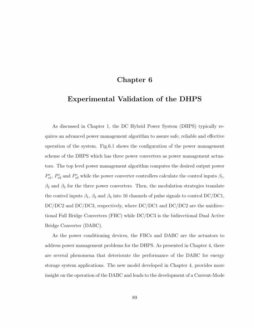
Chapter 6
Experimental Validation of the DHPS
As discussed in Chapter 1, the DC Hybrid Power System (DHPS) typically re-
quires an advanced power management algorithm to assure safe, reliable and effective
operation of the system. Fig.6.1 shows the configuration of the power management
scheme of the DHPS which has three power converters as power management actua-
tors. The top level power management algorithm computes the desired output power
P ∗o1, P ∗o2 and P ∗o3 while the power converter controllers calculate the control inputs β1,
β2 and β3 for the three power converters. Then, the modulation strategies translate
the control inputs β1, β2 and β3 into 16 channels of pulse signals to control DC/DC1,
DC/DC2 and DC/DC3, respectively, where DC/DC1 and DC/DC2 are the unidirec-
tional Full Bridge Converters (FBC) while DC/DC3 is the bidirectional Dual Active
Bridge Converter (DABC).
As the power conditioning devices, the FBCs and DABC are the actuators to
address power management problems for the DHPS. As presented in Chapter 4, there
are several phenomena that deteriorate the performance of the DABC for energy
storage system applications. The new model developed in Chapter 4, provides more
insight on the operation of the DABC and leads to the development of a Current-Mode
89
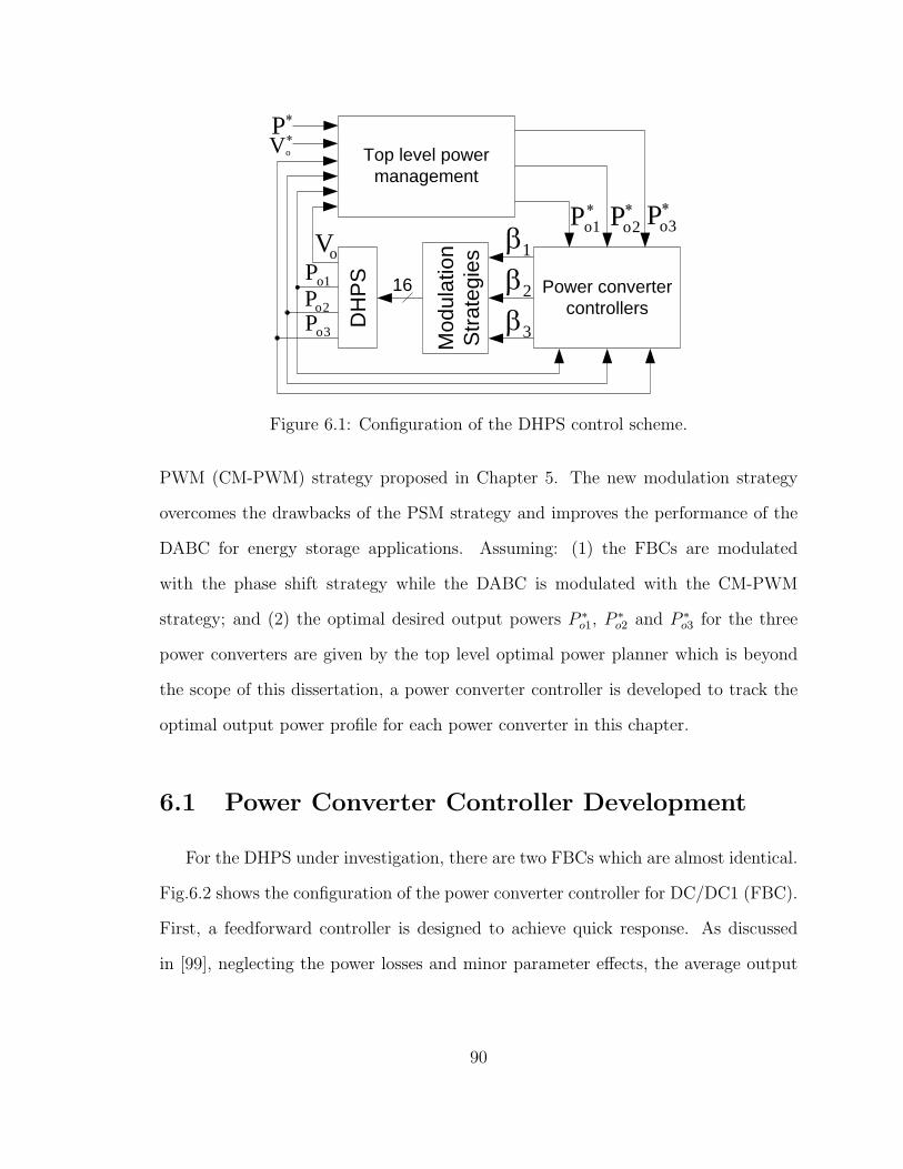
Top level power
management
1oP
Power converter
controllers
1
2
3
2oP
3oP
oV
1oP
2oP
3oP
PoV
Mo
du
latio
n
Str
ate
gie
s
16
DH
PS
Figure 6.1: Configuration of the DHPS control scheme.
PWM (CM-PWM) strategy proposed in Chapter 5. The new modulation strategy
overcomes the drawbacks of the PSM strategy and improves the performance of the
DABC for energy storage applications. Assuming: (1) the FBCs are modulated
with the phase shift strategy while the DABC is modulated with the CM-PWM
strategy; and (2) the optimal desired output powers P ∗o1, P ∗o2 and P ∗o3 for the three
power converters are given by the top level optimal power planner which is beyond
the scope of this dissertation, a power converter controller is developed to track the
optimal output power profile for each power converter in this chapter.
6.1 Power Converter Controller Development
For the DHPS under investigation, there are two FBCs which are almost identical.
Fig.6.2 shows the configuration of the power converter controller for DC/DC1 (FBC).
First, a feedforward controller is designed to achieve quick response. As discussed
in [99], neglecting the power losses and minor parameter effects, the average output
90
1βfb1β*1oP 1oP++
− +
ff1β
Figure 6.2: Configuration of the power management control scheme for a FBC.
power over the half switching cycle is
Po1 =β2
1TV1(n1V1 − Vo)4n1L1
. (6.1)
As a power converter with 10kHz switching frequency, the time constant of the
FBC is at the millisecond level. Given that the time constant for a typical power
system such as a fuel cell power system is about several seconds, there is a significant
time scale separation between the dynamics of the power source and the power con-
verter. This fact suggests that we can assume that the input voltage V1 is constant
over several switching periods. Moreover, we assume that the DC bus voltage Vo is
regulated to V ∗o by the top level power management algorithm. Therefore, by substi-
tuting Po1 = P ∗o1 and Vo = V ∗o into (6.1), a feedforward controller can be derived to
drive the FBC to track P ∗o1 given by the top level power management algorithm. The
nonlinear feedforward controller can be expressed as:
β1ff =
√4n1L1P ∗o1
TV1(n1V1 − V ∗o ), (6.2)
where n1V1 − V ∗o > 0 since the FBC is an isolated buck converter.
The power flow model given by (6.1) neglects the minor parameter effects such as
that of the dead time and neglects losses on the transformer, power semiconductors
91
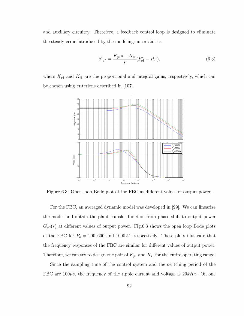
and auxiliary circuitry. Therefore, a feedback control loop is designed to eliminate
the steady error introduced by the modeling uncertainties:
β1fb =Kp1s+Ki1
s(P ∗o1 − Po1), (6.3)
where Kp1 and Ki1 are the proportional and integral gains, respectively, which can
be chosen using criterions described in [107].
0
10
20
30
40
50
60
70
80
Mag
nitu
de (d
B)
10-1
100
101
102
103
104
105
106
-90
-45
0
45
Pha
se (d
eg)
g
Frequency (rad/sec)
Po=200WPo=600WPo=1000W
Figure 6.3: Open-loop Bode plot of the FBC at different values of output power.
For the FBC, an averaged dynamic model was developed in [99]. We can linearize
the model and obtain the plant transfer function from phase shift to output power
Gpβ(s) at different values of output power. Fig.6.3 shows the open loop Bode plots
of the FBC for Po = 200, 600, and 1000W , respectively. These plots illustrate that
the frequency responses of the FBC are similar for different values of output power.
Therefore, we can try to design one pair of Kp1 and Ki1 for the entire operating range.
Since the sampling time of the control system and the switching period of the
FBC are 100µs, the frequency of the ripple current and voltage is 20kHz. On one
92
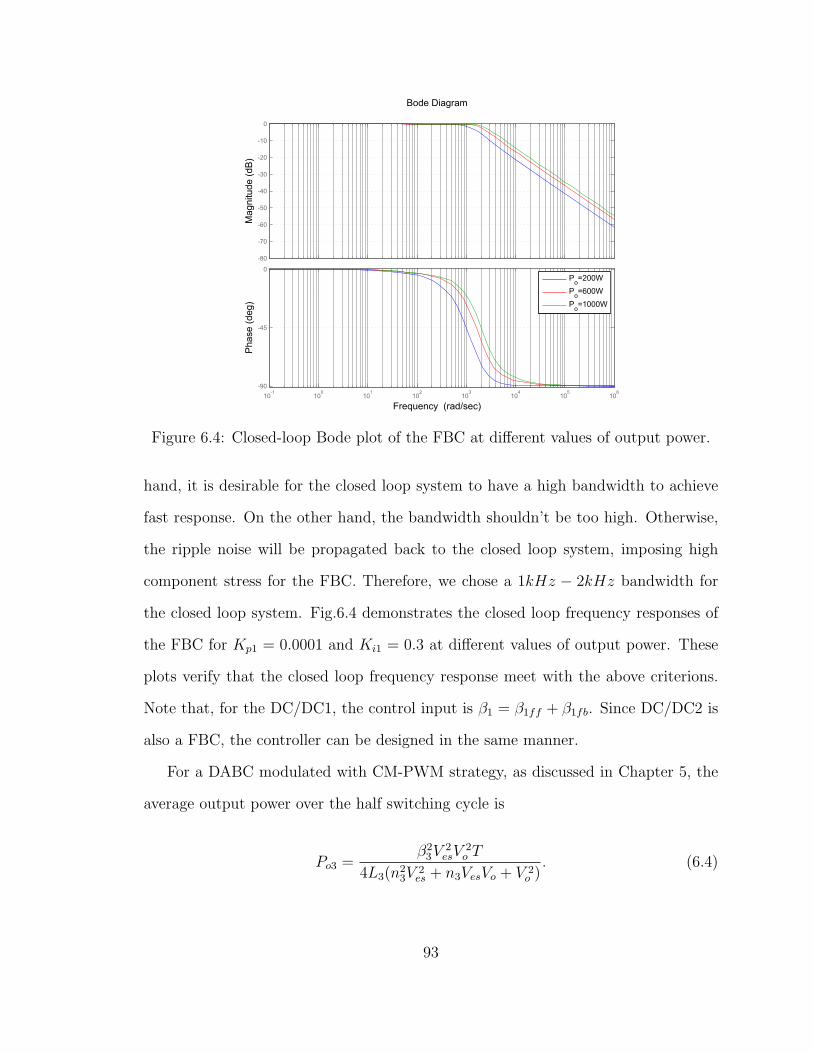
-80
-70
-60
-50
-40
-30
-20
-10
0
Mag
nitu
de (d
B)
10-1
100
101
102
103
104
105
106
-90
-45
0
Pha
se (d
eg)
Bode Diagram
Frequency (rad/sec)
Po=200WPo=600WPo=1000W
Figure 6.4: Closed-loop Bode plot of the FBC at different values of output power.
hand, it is desirable for the closed loop system to have a high bandwidth to achieve
fast response. On the other hand, the bandwidth shouldn’t be too high. Otherwise,
the ripple noise will be propagated back to the closed loop system, imposing high
component stress for the FBC. Therefore, we chose a 1kHz − 2kHz bandwidth for
the closed loop system. Fig.6.4 demonstrates the closed loop frequency responses of
the FBC for Kp1 = 0.0001 and Ki1 = 0.3 at different values of output power. These
plots verify that the closed loop frequency response meet with the above criterions.
Note that, for the DC/DC1, the control input is β1 = β1ff + β1fb. Since DC/DC2 is
also a FBC, the controller can be designed in the same manner.
For a DABC modulated with CM-PWM strategy, as discussed in Chapter 5, the
average output power over the half switching cycle is
Po3 =β2
3V2esV
2o T
4L3(n23V
2es + n3VesVo + V 2
o ). (6.4)
93
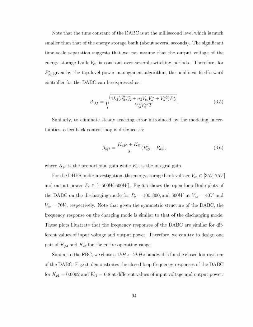
Note that the time constant of the DABC is at the millisecond level which is much
smaller than that of the energy storage bank (about several seconds). The significant
time scale separation suggests that we can assume that the output voltage of the
energy storage bank Ves is constant over several switching periods. Therefore, for
P ∗o3 given by the top level power management algorithm, the nonlinear feedforward
controller for the DABC can be expressed as:
β3ff =
√4L3(n2
3V2es + n3VesV ∗o + V ∗2o )P ∗o3
V 2esV
∗2o T
. (6.5)
Similarly, to eliminate steady tracking error introduced by the modeling uncer-
tainties, a feedback control loop is designed as:
β3fb =Kp3s+Ki3
s(P ∗o3 − Po3), (6.6)
where Kp3 is the proportional gain while Ki3 is the integral gain.
For the DHPS under investigation, the energy storage bank voltage Ves ∈ [35V, 75V ]
and output power Po ∈ [−500W, 500W ]. Fig.6.5 shows the open loop Bode plots of
the DABC on the discharging mode for Po = 100, 300, and 500W at Ves = 40V and
Ves = 70V , respectively. Note that given the symmetric structure of the DABC, the
frequency response on the charging mode is similar to that of the discharging mode.
These plots illustrate that the frequency responses of the DABC are similar for dif-
ferent values of input voltage and output power. Therefore, we can try to design one
pair of Kp3 and Ki3 for the entire operating range.
Similar to the FBC, we chose a 1kHz−2kHz bandwidth for the closed loop system
of the DABC. Fig.6.6 demonstrates the closed loop frequency responses of the DABC
for Kp1 = 0.0002 and Ki1 = 0.8 at different values of input voltage and output power.
94
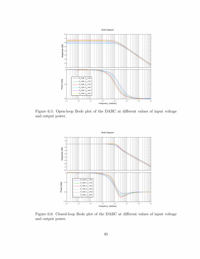
0
10
20
30
40
50
60
70
80
Mag
nitu
de (d
B)
10-1
100
101
102
103
104
105
106
-90
-45
0
Pha
se (d
eg)
Bode Diagram
Frequency (rad/sec)
Po=100, Ves=70V
Po=300, Ves=70V
Po=500, Ves=70V
Po=100, Ves=40V
Po=300, Ves=40V
Po=500, Ves=40V
Figure 6.5: Open-loop Bode plot of the DABC at different values of input voltageand output power.
-80
-70
-60
-50
-40
-30
-20
-10
0
10
20
Mag
nitu
de (d
B)
10-1
100
101
102
103
104
105
106
-135
-90
-45
0
Pha
se (d
eg)
Bode Diagram
Frequency (rad/sec)
Po=100, Ves=70V
Po=300, Ves=70V
Po=500, Ves=70V
Po=100, Ves=40V
Po=300, Ves=40V
Po=500, Ves=40V
Figure 6.6: Closed-loop Bode plot of the DABC at different values of input voltageand output power.
95

These plots verify that the closed loop frequency response meet with the criterion.
Table6.1 summarizes the gains for the feedback controller of the three power con-
verters.
Table 6.1: Feedback control gains of the power converters
DC/DC1 DC/DC2 DC/DC3Kp 0.0001 0.0001 0.0002Ki 0.3 0.3 0.8
6.2 Experimental Results
The power converter control algorithm is implemented on the DHPS testbed de-
scribed in Chapter 2. Suppose that there is a top level optimal power management
algorithm to calculate the power profile for each power converter, the goal of this
section is to verify whether the controller can quickly and accurately track the power
profile for each power converter during both the charging and discharging modes of
the energy storage system.
Fig.6.7 shows the experimental results of the charging mode when there is a step
change for the power demands P ∗o1 and P ∗o2 while there is a constant −400W power Po3
charging the energy storage bank. Both the power converters DC/DC1 and DC/DC2
track their power demands P ∗o1 and P ∗o2 with the milliseconds level settling time while
only a small deviation for the Po3 is observed.
Fig.6.8 presents the experimental results in the presence of a step change for the
power demand P ∗o3. Initial P ∗o3 is −400W . A step-down change of the power demand
P ∗o3 is then applied to command the bidirectional DABC operating with the idling
mode (0W input/output power). Meanwhile, the output power of both DC/DC1 and
DC/DC2 are reduced.
96
0 0.01 0.02 0.03 0.04 0.05 0.06 0.07 0.08 0.09 0.1200
400
600
Po1
Pow
er, [
W]
0 0.01 0.02 0.03 0.04 0.05 0.06 0.07 0.08 0.09 0.1800
1000
1200Po2
Pow
er, [
W]
0 0.01 0.02 0.03 0.04 0.05 0.06 0.07 0.08 0.09 0.1-600-400-200
0
Po3
Pow
er, [
W]
0 0.01 0.02 0.03 0.04 0.05 0.06 0.07 0.08 0.09 0.10
0.5
1Control inputs
Time, [s]
DemandResponse
β1
β2
β3
Figure 6.7: Experimental results of constant power charging mode.
0 0.005 0.01 0.015 0.02 0.025 0.03 0.035 0.04 0.045 0.05150
200
250
300
Pow
er, [
W]
Po1
0 0.005 0.01 0.015 0.02 0.025 0.03 0.035 0.04 0.045 0.05
800
1000
1200Po2
Pow
er, [
W]
0 0.005 0.01 0.015 0.02 0.025 0.03 0.035 0.04 0.045 0.05
-400
-200
0
Po3
Pow
er, [
W]
0 0.005 0.01 0.015 0.02 0.025 0.03 0.035 0.04 0.045 0.050
0.5
1
Time, [s]
Control inputs
DemandResponse
β1
β2
β3
Figure 6.8: Experimental results of step-change power charging mode.
97
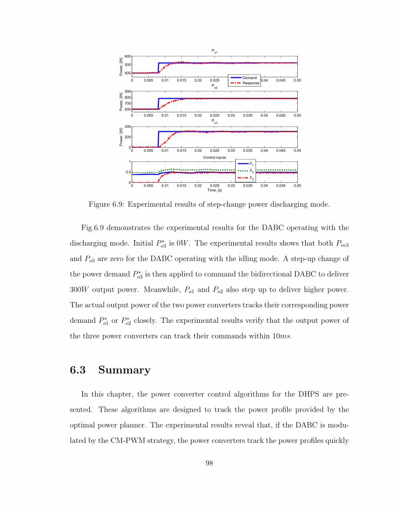
0 0.005 0.01 0.015 0.02 0.025 0.03 0.035 0.04 0.045 0.05
400
500
600
Pow
er, [
W]
Po1
0 0.005 0.01 0.015 0.02 0.025 0.03 0.035 0.04 0.045 0.05600700800900
Po2
Pow
er, [
W]
0 0.005 0.01 0.015 0.02 0.025 0.03 0.035 0.04 0.045 0.050
200
400Po3
Pow
er, [
W]
0 0.005 0.01 0.015 0.02 0.025 0.03 0.035 0.04 0.045 0.050
0.5
1
Time, [s]
Control inputs
DemandResponse
β1
β2
β3
Figure 6.9: Experimental results of step-change power discharging mode.
Fig.6.9 demonstrates the experimental results for the DABC operating with the
discharging mode. Initial P ∗o3 is 0W . The experimental results shows that both Pin3
and Po3 are zero for the DABC operating with the idling mode. A step-up change of
the power demand P ∗o3 is then applied to command the bidirectional DABC to deliver
300W output power. Meanwhile, Po1 and Po2 also step up to deliver higher power.
The actual output power of the two power converters tracks their corresponding power
demand P ∗o1 or P ∗o2 closely. The experimental results verify that the output power of
the three power converters can track their commands within 10ms.
6.3 Summary
In this chapter, the power converter control algorithms for the DHPS are pre-
sented. These algorithms are designed to track the power profile provided by the
optimal power planner. The experimental results reveal that, if the DABC is modu-
lated by the CM-PWM strategy, the power converters track the power profiles quickly
98

and closely.
Although the experimental results verified the effectiveness of the controllers, it
is a more challenging control problem to achieve control objectives without violating
the physical constraints of the power converters. The MPC scheme which can be used
to effectively handle constraints will be applied to a FBC in the next chapter.
99

Chapter 7
Model Predictive Control of the Full Bridge
Converter
Motivated by the challenges of power converter control and recent development
of advanced control and optimization algorithms, this chapter investigates the MPC
schemes for the Full Bridge Converter (FBC) control. The control objective is to reg-
ulate the output voltage without violating peak current constraint. Moreover, since
the FBC is a highly nonlinear system with a wide operating range and fast dynamics,
it is interesting to compare the closed loop performance and computational time for
the linear MPC and nonlinear MPC schemes. The inductor peak current constraint
of the full bridge DC/DC converter will be first presented. Then an observer design
for states and parameter estimation using a large signal dynamic model is introduced.
After that, the voltage regulation problem is formulated as a MPC problem using ei-
ther a linear or a nonlinear model to predict the future plant behavior, while the peak
current protection requirement is formulated as a nonlinear constraint. Finally, the
InPA-SQP solver is interpreted, followed by experimental results that confirm the ef-
fectiveness of the proposed MPC algorithm and compare the closed loop performance
and computation time of the two MPC schemes.
100
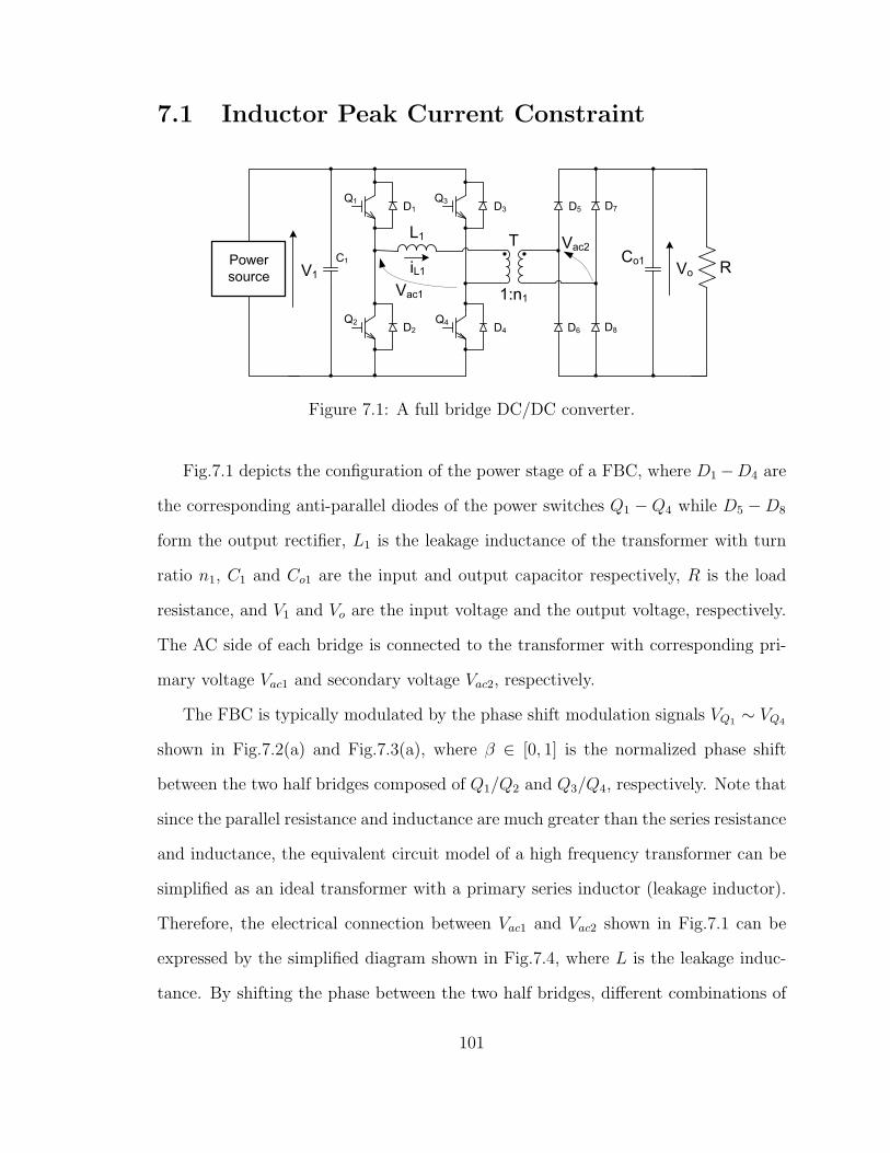
7.1 Inductor Peak Current Constraint
Q1
Q2 Q4
1
1
o1
Q3
1 o
D1
D2
D3
D4
D5
D6
D7
D8
L1C1
ac1
ac2
Figure 7.1: A full bridge DC/DC converter.
Fig.7.1 depicts the configuration of the power stage of a FBC, where D1−D4 are
the corresponding anti-parallel diodes of the power switches Q1 −Q4 while D5 −D8
form the output rectifier, L1 is the leakage inductance of the transformer with turn
ratio n1, C1 and Co1 are the input and output capacitor respectively, R is the load
resistance, and V1 and Vo are the input voltage and the output voltage, respectively.
The AC side of each bridge is connected to the transformer with corresponding pri-
mary voltage Vac1 and secondary voltage Vac2, respectively.
The FBC is typically modulated by the phase shift modulation signals VQ1 ∼ VQ4
shown in Fig.7.2(a) and Fig.7.3(a), where β ∈ [0, 1] is the normalized phase shift
between the two half bridges composed of Q1/Q2 and Q3/Q4, respectively. Note that
since the parallel resistance and inductance are much greater than the series resistance
and inductance, the equivalent circuit model of a high frequency transformer can be
simplified as an ideal transformer with a primary series inductor (leakage inductor).
Therefore, the electrical connection between Vac1 and Vac2 shown in Fig.7.1 can be
expressed by the simplified diagram shown in Fig.7.4, where L is the leakage induc-
tance. By shifting the phase between the two half bridges, different combinations of
101
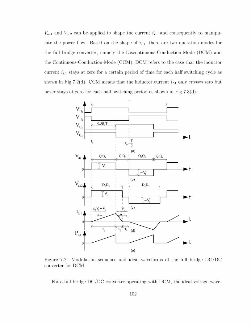
Vac1 and Vac2 can be applied to shape the current iL1 and consequently to manipu-
late the power flow. Based on the shape of iL1, there are two operation modes for
the full bridge converter, namely the Discontinuous-Conduction-Mode (DCM) and
the Continuous-Conduction-Mode (CCM). DCM refers to the case that the inductor
current iL1 stays at zero for a certain period of time for each half switching cycle as
shown in Fig.7.2(d). CCM means that the inductor current iL1 only crosses zero but
never stays at zero for each half switching period as shown in Fig.7.3(d).
T
(a)
(b)
(d)
(e)
1oP
1Li
1acV
1QV
41QQ
1V
1V−
31QQ 32QQ 42QQ
11
o11
LnVVn −
11
o
LnV
−(c)
2acV 85DD
oV
oV−
76DD
aτ bτ cτ
0
0
0
0
0t2Tt0 +
T0.5 1β2Q
V
4QV
3QV
Figure 7.2: Modulation sequence and ideal waveforms of the full bridge DC/DCconverter for DCM.
For a full bridge DC/DC converter operating with DCM, the ideal voltage wave-
102
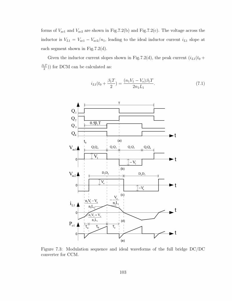
forms of Vac1 and Vac2 are shown in Fig.7.2(b) and Fig.7.2(c). The voltage across the
inductor is VL1 = Vac1 − Vac2/n1, leading to the ideal inductor current iL1 slope at
each segment shown in Fig.7.2(d).
Given the inductor current slopes shown in Fig.7.2(d), the peak current (iL1(t0 +
β1T2
)) for DCM can be calculated as:
iL1(t0 +β1T
2) =
(n1V1 − Vo)β1T
2n1L1
. (7.1)
T
(a)
(b)
(e)
1oP
1Li
1acV
1Q
41QQ
1V1V−
31QQ 32QQ 42QQ
11
o
LnV
−(c)
2acV 85DD
oV
oV−
76DD
2Q
3Q
4Q
(d)11
o11
LnVVn +
aτ bτ cτ
0
0
0
0
11
o11
LnVVn −
0t
T0.5 1β
Figure 7.3: Modulation sequence and ideal waveforms of the full bridge DC/DCconverter for CCM.
103
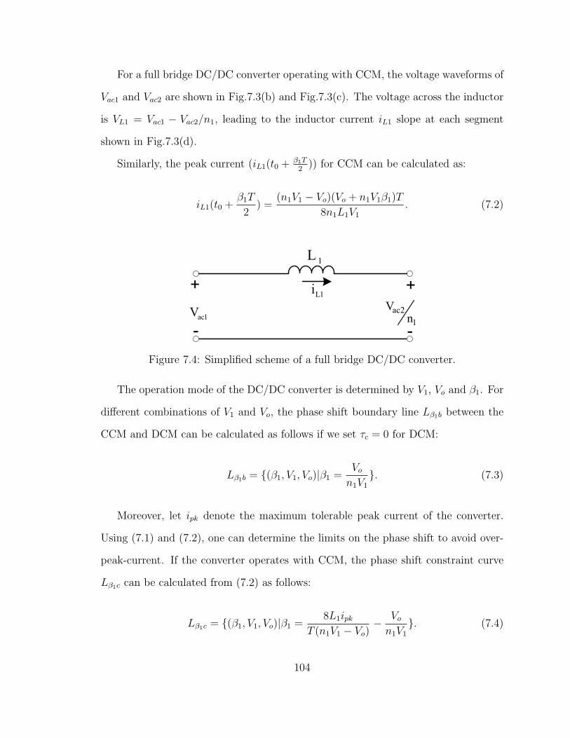
For a full bridge DC/DC converter operating with CCM, the voltage waveforms of
Vac1 and Vac2 are shown in Fig.7.3(b) and Fig.7.3(c). The voltage across the inductor
is VL1 = Vac1 − Vac2/n1, leading to the inductor current iL1 slope at each segment
shown in Fig.7.3(d).
Similarly, the peak current (iL1(t0 + β1T2
)) for CCM can be calculated as:
iL1(t0 +β1T
2) =
(n1V1 − Vo)(Vo + n1V1β1)T
8n1L1V1
. (7.2)
12acn
V1acV
1Li
1L
Figure 7.4: Simplified scheme of a full bridge DC/DC converter.
The operation mode of the DC/DC converter is determined by V1, Vo and β1. For
different combinations of V1 and Vo, the phase shift boundary line Lβ1b between the
CCM and DCM can be calculated as follows if we set τc = 0 for DCM:
Lβ1b = (β1, V1, Vo)|β1 =Von1V1
. (7.3)
Moreover, let ipk denote the maximum tolerable peak current of the converter.
Using (7.1) and (7.2), one can determine the limits on the phase shift to avoid over-
peak-current. If the converter operates with CCM, the phase shift constraint curve
Lβ1c can be calculated from (7.2) as follows:
Lβ1c = (β1, V1, Vo)|β1 =8L1ipk
T (n1V1 − Vo)− Von1V1
. (7.4)
104
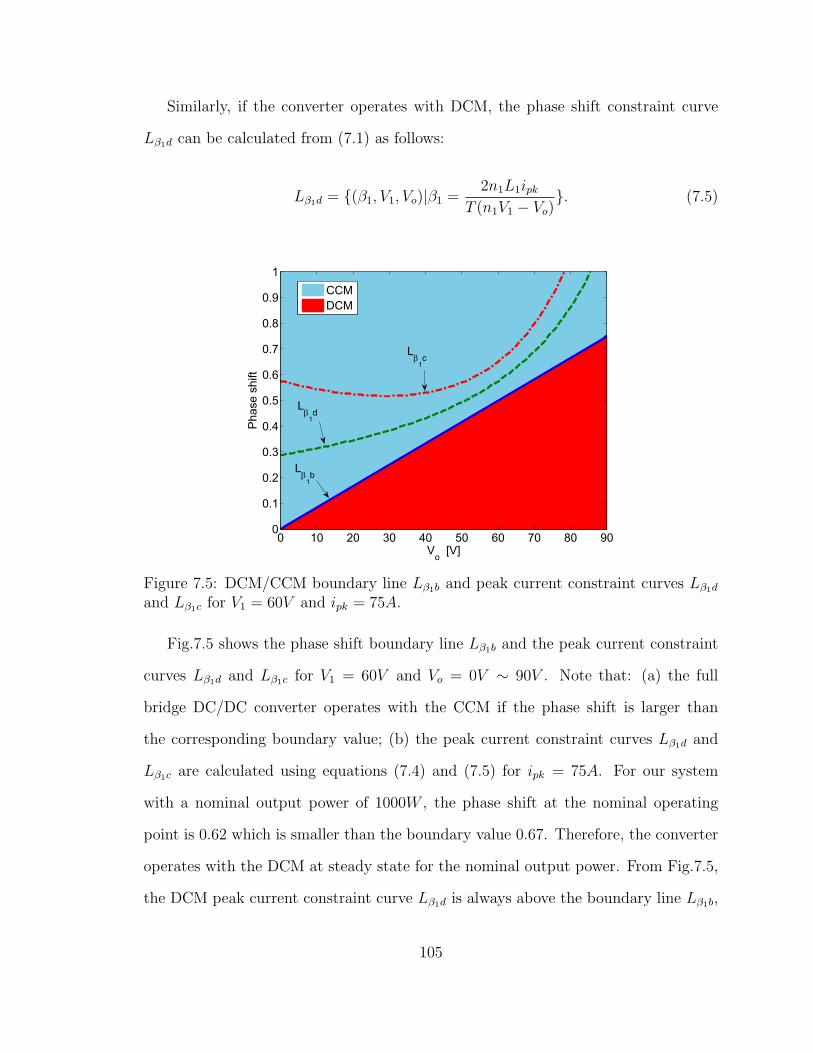
Similarly, if the converter operates with DCM, the phase shift constraint curve
Lβ1d can be calculated from (7.1) as follows:
Lβ1d = (β1, V1, Vo)|β1 =2n1L1ipk
T (n1V1 − Vo). (7.5)
Lβ
1b
Lβ
1c
Lβ
1d
Vo [V]
Pha
se s
hift
0 10 20 30 40 50 60 70 80 900
0.1
0.2
0.3
0.4
0.5
0.6
0.7
0.8
0.9
1CCMDCM
Figure 7.5: DCM/CCM boundary line Lβ1b and peak current constraint curves Lβ1d
and Lβ1c for V1 = 60V and ipk = 75A.
Fig.7.5 shows the phase shift boundary line Lβ1b and the peak current constraint
curves Lβ1d and Lβ1c for V1 = 60V and Vo = 0V ∼ 90V . Note that: (a) the full
bridge DC/DC converter operates with the CCM if the phase shift is larger than
the corresponding boundary value; (b) the peak current constraint curves Lβ1d and
Lβ1c are calculated using equations (7.4) and (7.5) for ipk = 75A. For our system
with a nominal output power of 1000W , the phase shift at the nominal operating
point is 0.62 which is smaller than the boundary value 0.67. Therefore, the converter
operates with the DCM at steady state for the nominal output power. From Fig.7.5,
the DCM peak current constraint curve Lβ1d is always above the boundary line Lβ1b,
105

so the peak current constraint will not be violated if the power converter operates
with DCM at steady state. However, for the cases of starting process and overload,
the power converter operates at CCM, where the CCM peak current constraint may
be violated. Therefore, an active constraint enforcement mechanism needs to be
incorporated to protect the converter.
7.2 Nonlinear Dynamic Model and Observer
Since the FBC is a highly nonlinear system with a wide operating range, it is
desirable to employ a model based control design approach to achieve satisfactory
closed loop system performance. Since the full bridge DC/DC converter has a wide
operating range, it is necessary to derive a large signal dynamic model for the system
to facilitate the model based control design. Using the analysis results presented in
the previous section and following the same technique in [33], the dynamic model of
the full bridge DC/DC converter was derived in [99] and can be written as:
diL1
dt=β1V1
L1
− 4iL1Voβ1T (n1V1 − Vo)
, (7.6)
dVodt
=iL1
n1Co1− VoRCo1
, (7.7)
y = Vo. (7.8)
Note that: iL1 and Vo represent the average current and the average output voltage
over a switching period.
For the dynamic system represented by (7.6)-(7.8), the implementation of ad-
vanced control strategies requires the information of the load resistance R and the
average current iL1. The load resistance R is typically a bounded unknown parameter.
However, it is necessary to estimate this parameter for the NLMPC scheme. Mean-
106

while, if we use a current sensor to obtain iL1, on the one hand, the current sensor
must have high bandwidth to accurately reconstruct the current signal. On the other
hand, due to electromagnetic interference, it is often necessary to use a low-pass filter
to remove noise. However, a low-pass filter typically introduces additional phase lag
for the closed loop system. To overcome these drawbacks, we treat the load resistance
R as a state and use a nonlinear observer to estimate R and iL1 while keeping Vo as
the only measured variable. The nonlinear observer is expressed as follows:
diL1
dt=β1V1
L1
− 4iL1ˆVo
β1T (n1V1 − ˆVo)+H1(y − y), (7.9)
d ˆVodt
=ˆiL1
n1Co1−
ˆVoRCo1
+H2(y − y), (7.10)
dR
dt= H3(y − y), (7.11)
y = ˆVo. (7.12)
where H1, H2 and H3 are the nonlinear observer gains which can be chosen to achieve
fast convergence of the observer.
7.3 MPC Formulation
This section presents the formulation of the LMPC and NLMPC schemes for the
FBC. The control objective is to regulate the output voltage without violating the
peak current constraint. For a given inductor peak current ipk, the CCM peak current
(7.2) must satisfy
(n1V1 − Vo)(Vo + n1V1β1)T
8n1L1V1
≤ ipk. (7.13)
107

If we define x = [x1, x2]T = [iL1, Vo]T and u = β1, (7.13) can be rewritten in terms
the state variables and control input as:
E1(x, u) ≤ 0. (7.14)
where,
E1(x, u) =(n1V1 − x2)(x2 + n1V1u)
8n1L1V1
− ipkT.
Then, the peak current protection requirement can be formulated as a mixed states
and control input constraint for both LMPC and NLMPC schemes described in the
following two subsections.
7.3.1 Offset-Free Linear MPC Formulation
The dynamic system represented by (7.6)-(7.8) can be easily linearized at the
nominal operating point (Vo = 80V and Po = 1KW ) with nominal value xo = [25, 80]T
and uo = 0.62. Let x1 = iL1 − 25, x2 = Vo − 80 and u = β1 − 0.62, the system can be
transformed into its discrete-time version for a specific sampling time:
x(k + 1) = f(x(k), u(k)) := Ax(k) +Bu(k), (7.15)
y(k) = Fx(k). (7.16)
where A ∈ Rn×n, B ∈ Rn×m, F ∈ Rm×n. Note that n = 2 and m = 1 for the system
under investigation.
108

The peak current constraint (7.14) can be rewritten as:
E1(x(k), u(k)) =(n1V1 − (xo2 + x2(k)))(xo2 + x2(k))
8nLV1
+(n1V1 − (xo2 + x2(k)))n(uo + u(k))
8n1L1
− ipkT.
(7.17)
To eliminate the steady state error, the offset-free MPC has been developed in
previous studies [82–85]. For this application, the plant model represented by (7.15)-
(7.16) can be augmented with a constant disturbance model:
x(k + 1) = Ax(k) +Bu(k) +Bdd(k), (7.18)
d(k + 1) = d(k), (7.19)
y(k) = Fx(k). (7.20)
Based on the augmented model, the state and disturbance estimator can be de-
signed as:
ˆx(k + 1) = Aˆx(k) +Bu(k) +Bdd(k)
+H4(−Fx(k) + F ˆx(k)), (7.21)
d(k + 1) = d(k) +H5(−Fx(k) + F ˆx(k)). (7.22)
where H4 and H5 are observer gains which are designed to achieve fast convergence
[83,84].
The steady state values of the observer is
A− I B
F 0
ˆxs
us
=
−Bdds
0
(7.23)
109

where us is the steady state input while ˆxs and ds are steady state of the observed
state and disturbance, respectively.
Then the MPC online optimization problem can be formulated as follows: let
∆x(k) = x(k) − ˆxs and ∆u(k) = u(k) − us; at the time instant k, the state of the
system, x(k), is observed and the following optimal control problem PN(∆x(k)) is
solved
PN(∆x(k)) : V ∗N(∆x(k)) = min∆x,∆u
VN(∆x(k),∆u) (7.24)
VN(∆x(k),∆u) =k+N−1∑j=k
G(∆x(j),∆u(j)) + Φ(∆x(N))
subject to
∆x(j + 1) = A∆x(k) +B∆u(k), (7.25)
∆x(0) = ∆x(k) ∈ Rn; (7.26)
E(∆x(·),∆u(·)) ≤ 0, E : Rn+m → Rl. (7.27)
where,
∆u = ∆u(k),∆u(k + 1), ...,∆u(k +N − 1), (7.28)
is the control sequence,
∆x = ∆x(k),∆x(k + 1), ...,∆x(k +N − 1) (7.29)
is the state trajectory,
G(∆x(j),∆u(j)) =∆x(j)TQ1∆x(j) + ∆u(j)TW1∆u(j),
j = k, k + 1, · · · , k +N − 1
(7.30)
110

and Φ(∆x(N)) is the penalty for the final states. Q1 ∈ Rn×n and W1 ∈ Rm×m are
the corresponding weighting matrices which are used to penalize the deviation of the
output and the control input to their corresponding desired value, N is the prediction
horizon, and E(∆x(k),∆u(k)) is the constraint matrix and can be written as follows
with l = 3: ∆u(j) + us − (1− uo)
−∆u(j)− us − uo
E1(∆x(j) + ˆxs,∆u(j) + us)
. (7.31)
Note that the first two components are derived because of the boundedness of the
phase shift (β1 ∈ [0, 1]) and each component in (7.31) is bounded above by zero.
7.3.2 Nonlinear MPC Formulation
For the nonlinear dynamic system represented by (7.6)-(7.8), the nonlinear system
can be transformed into its discrete-time version for a specific sampling time:
x(k + 1) = f(x(k), u(k)), (7.32)
y(k) = Fx(k). (7.33)
The CCM peak current constraint (7.14) can be rewritten as:
E1(x(k), u(k)) =(n1V1 − x2(k))(x2(k) + n1V1u(k))
8n1L1V1
− ipkT. (7.34)
Then the MPC online optimization problem can be formulated as follows: at the
time instant k, the state of the system, x(k), is observed and the following optimal
111

control problem PN(x(k)) is solved
PN(x(k)) : V ∗N(x(k)) = minx,uVN(x(k),u) (7.35)
VN(x(k),u) =k+N−1∑j=k
G(x(j), u(j)) + Φ(x(N))
subject to
x(j + 1) = f(x(j), u(j)), f : Rn+m → Rn; (7.36)
x(0) = x(k) ∈ Rn; (7.37)
E(x(·), u(·)) ≤ 0, E : Rn+m → Rl. (7.38)
where,
u = u(k), u(k + 1), ..., u(k +N − 1), (7.39)
is the control sequence,
x = x(k), x(k + 1), ..., x(k +N − 1), (7.40)
is the state trajectory,
G(x(j), u(j)) = x(j)TQ2x(j) + u(j)TW2u(j), j = k, k + 1, · · · , k +N − 1 (7.41)
and Φ(x(N)) is the penalty for the final states. Q2 ∈ Rn×n and W2 ∈ Rm×m are
the corresponding weighting matrices which are used to penalize the deviation of
the output and the control input from their corresponding desired value, N is the
prediction horizon, and E(x(k), u(k)) is the constraint matrix and can be written as
112

follows with l = 3: u(j)− 1
−u(j)
E1(x(j), u(j))
. (7.42)
Note that the first two components are derived because of the boundedness of the
phase shift (β1 ∈ [0, 1]) and each component in (7.42) is bounded above by zero.
Since the full bridge DC/DC converter has the millisecond level time constant, a
rational choice of the sampling time is between 100µs and 400µs [101]. We choose
300µs as the sampling time for the controller. The length of the prediction hori-
zon N is a basic tuning parameter for MPC controllers. However, we have to chose
N ≥ 3 to ensure that the prediction time length is no less than the time constant
of the full bridge DC/DC converter. We will compare the closed-loop system per-
formance with different prediction horizons for both the linear and nonlinear model
based MPC algorithms. The weighting matrices Q1, Q2, W1 and W2 are the main
tuning parameters of the quadratic cost functions (7.30) and (7.41) to shape the
closed-loop response for desired performance. The closed loop performance crite-
ria are defined as: (1) to achieve fast output response with small output overshoot;
and (2) to avoid high frequency control input oscillations which might cause high
slew rate for the inductor current and high stress for switching components. We
evaluate the performance for different combinations of the weighting matrix using a
virtual hardware for controller tuning. The virtual hardware is developed using MAT-
LAB/Simulink/SimPowerSystems toolbox and has the same parameters as the real
hardware. The preliminary evaluation results lead to the choice of Q1 = [0 0; 0 0.01],
Q2 = [0 0; 0 0.2] and W1 = W2 = 1. Furthermore, we do not penalize the final states
x(N) and ∆x(N), meaning Φ(x(N)) = Φ(∆x(N)) = 0.
Given the fast dynamics of the converter, we have to apply fast algorithms to solve
113

the above optimization problem online in real-time. We employ a method, which we
refer to as the InPA-SQP approach, to solve the nonlinearly constrained optimization
problems for LMPC and NLMPC of the full bridge DC/DC converter.
7.4 InPA-SQP Algorithm
We now introduce a method, which we refer to as the Integrated Perturbation
Analysis and Sequential Quadratic Programming (InPA-SQP) approach [90, 91], for
the MPC implementation. It is worthwhile to point out that, for simplicity, we
only interpret the InPA-SQP algorithm for the NLMPC case. For offset-free LMPC
problem, one can simply replace x(·) and u(·) with their counterparts ∆x(·) and ∆u(·)
and follow the same procedure to solve the nonlinearly constrained optimal control
problem.
According to the MPC strategy, at the time instant k, the state of the system,
x(k), is observed and the optimal control problem PN(x(k)) defined by (7.35)−(7.38)
is solved. The resulting optimal control sequence is
u∗(x(k)) = u∗(k;x(k)), u∗(k + 1;x(k)), ..., u∗(k +N − 1;x(k)), (7.43)
the optimal state trajectory is
x∗(x(k)) = x∗(k;x(k)), x∗(k + 1;x(k)), · · · , x∗(k +N ;x(k)), (7.44)
where x∗(k;x(k)) = x(k) and the model predictive control law at the time instant k
is defined as:
h(x(k)) := u∗(k;x(k)). (7.45)
114
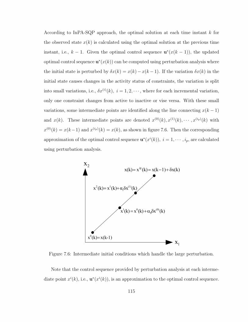
According to InPA-SQP approach, the optimal solution at each time instant k for
the observed state x(k) is calculated using the optimal solution at the previous time
instant, i.e., k − 1. Given the optimal control sequence u∗(x(k − 1)), the updated
optimal control sequence u∗(x(k)) can be computed using perturbation analysis where
the initial state is perturbed by δx(k) = x(k)−x(k− 1). If the variation δx(k) in the
initial state causes changes in the activity status of constraints, the variation is split
into small variations, i.e., δx(i)(k), i = 1, 2, · · · , where for each incremental variation,
only one constraint changes from active to inactive or vise versa. With these small
variations, some intermediate points are identified along the line connecting x(k− 1)
and x(k). These intermediate points are denoted x(0)(k), x(1)(k), · · · , x(ip)(k) with
x(0)(k) = x(k−1) and x(ip)(k) = x(k), as shown in figure 7.6. Then the corresponding
approximation of the optimal control sequence u∗(xi(k)), i = 1, · · · , ip, are calculated
using perturbation analysis.
1)-x(k(k)x0 =
)k(x)k(x)k(x )0(0
01 δα+=
(k)δxα(k)x(k)x (1)1
12 +=
δx(k)1)x(k(k)xx(k) ip +−==
1x
2x
Figure 7.6: Intermediate initial conditions which handle the large perturbation.
Note that the control sequence provided by perturbation analysis at each interme-
diate point xi(k), i.e., u∗(xi(k)), is an approximation to the optimal control sequence.
115

Therefore, the error can accumulate and the optimality condition may be lost at these
intermediate steps. To compensate for this error and maintain the optimality of the
approximate solution, we use a special formulation of SQP with active set method
to modify the perturbation analysis algorithm. This special formulation allows us to
cast the solution of the SQP into a formula which is similar to that of the pertur-
bation analysis, thereby facilitating the seamless integration of perturbation analysis
and SQP to speed up the calculation of the optimal solution. The detailed algorithm
is presented as follows for the general nonlinear MPC implementation:
At the time instant k, we need to solve PN(x(k)), given the solution of PN(x(k−
1)). We consider the general case where functions G(x(·), u(·)), G : Rn+m → R,
Φ(x(·)), Φ : Rn+m → R, f(x(·), u(·)), E(x(·), u(·)) are twice continuously differen-
tiable with respect to x and u. Moreover, let us define the Hamiltonian function H
at prediction time instants k, k + 1, · · · , k +N − 1 as
H(j) :=G(x(j), u(j)) + λ(j + 1)Tf(x(j), u(j)) + µ(j)TE(x(j), u(j)),
j = k, · · · , k +N − 1
(7.46)
where, µ(j) is the Lagrange multiplier associated with the inequality constraint (7.38)
and λ(j + 1) is the Lagrange multiplier associated with equality constraint (7.36) at
the prediction time instant j, where j > k.
Since we know the solution of PN(x(k− 1)) at the time instant k, by treating the
initial state x(k) as x(k − 1) plus its perturbation δx(k) = x(k) − x(k − 1), we go
through the following steps to calculate the optimal solution for the initial state x(k):
1. Measure x(k) and assume u∗(x(k−1)) and x(k−1) are given from the previous
time instant k − 1.
2. Set i = 0, δx(0)(k) = x(k) − x(k − 1), x(0)(j) = x∗(j;x(k − 1)), and u(0)(j) =
116

u∗(j;x(k − 1)), for j = k, · · · , k +N − 1.
3. Calculate the state and control variations δx(i)(j+1) and δu(i)(j), j ∈ [k : k+N ],
for the initial state perturbation δx(i)(k), as follows:
δu(i)(j)=−[I 0]K0(j)×
Zux(j)δx(i)(j)+fTu (j)T (j + 1)+Hu(j)
Eax(j)δx(i)(j)
,δx(i)(j + 1) = fx(j)δx
(i)(j) + fu(j)δu(i)(j),
and δx(i)(k) given,
(7.47)
where Hu(j) is the partial derivative of the Hamiltonian function with respect
to control u at the prediction time instant j, and
Zuu(j) = Huu(j) + fTu (j)S(j + 1)fu(j),
Zux(j) = Zxu(j)T = Hux(j) + fTu (j)S(j + 1)fx(j),
Zxx(j) = Hxx(j) + fTx (j)S(j + 1)fx(j),
(7.48)
with S(j) being calculated by the following backward recursive equations
S(k +N) = Φxx(k +N), T (k +N) = 0,
S(j) = Zxx(j)− [Zxu(j) EaxT (j)]K0(j)
Zux(j)
Eax(j)
,T (j)=fTx (j)T (j +1)−[Zxu(j) E
axT (j)]K0(j)
fTu (j)T (j +1)+Hu(j)
0
,(7.49)
117

and when the constraint is active, K0(·) is given by
K0(j) =
Zuu(j) EauT (j)
Eau(j) 0
−1
, (7.50)
where Ea(j) is a vector consisting of those elements of the vector E(x(j), u(j))
whose corresponding inequality constraints are active. If no constraint is active
at the prediction time instant j,
K0(j) = [Zuu(j)]−1 , j = k, · · · , k +N − 1. (7.51)
Moreover, when the constraint is active, calculate the optimal Lagrange mul-
tiplier variation [δµ(i)(k), δµ(i)(k + 1), · · · , δµ(i)(k + N − 1)] corresponding to
initial state variation δx(i)(k) as follows:
δµ(i)(j) =− [0 I]K0(j)×
Zux(j)δx(i)(j)+fTu (j)T (j + 1)+Hu(j)
Eax(j)δx(i)(j)
. (7.52)
All matrices are evaluated at x(i)(·) and u(i)(·).
4. Find the smallest αi among αik such that the perturbation αiδx(i)(k) changes
the status of the constraint at least at one instant, namely:
αi = minkαik, k = 0, · · · , N − 1, and 0 ≤ αik ≤ 1.
If for all k ∈ [0 : N − 1], either αik < 0 or αik > 1, set αi = 1.
118

5. If αi = 1, set
ui+1(·) = ui(·) + δu(i)(·)
xi+1(·) = xi(·) + δx(i)(·)(7.53)
and set the solution u∗(x(k)) = u(i+1)(·). Otherwise:
• If αi = 0, change the activity status of the corresponding constraint ac-
cordingly. That is, if αi corresponds an active (inactive) constraint, set
the constraint inactive (active). Go to step 2.
• If αi < 1 set
ui+1(·) = ui(·) + αiδu(i)(·)
xi+1(·) = xi(·) + αiδx(i)(·)
(7.54)
and
δx(i+1)(k) = (1− αi)δx(i)(k),
xi+1(k) = xi(k) + αiδx(i)(k),
i = i+ 1.
Go to step 3.
Fig.7.7 shows the flowchart of the InPA-SQP algorithm. The perturbed optimal
control solution corresponding to the large perturbation δx(k) can be approximated
by augmenting the nominal solution with the intermediate ones as:
u∗(j;x(k)) +∑i
δu(i)(j), j = k, · · · , k +N − 1.
119
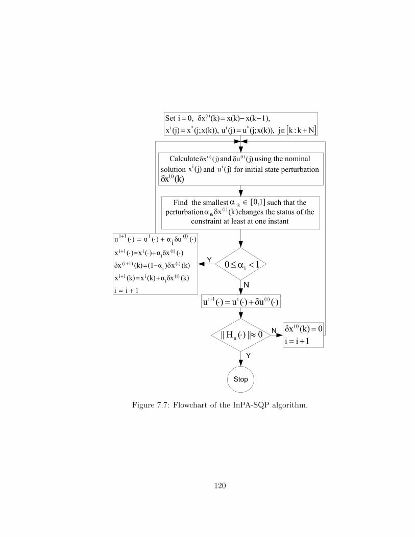
[ ]Nk:kjx(k)),(j;u(j)ux(k)),(j;x(j)x1),x(kx(k)(k)δx0,iSet
*i*i
(i)
+∈==−−==
)j(x )i(δ
)j(xi )j(ui)j(u )i(δ
)k(x )i(δ
]1,0[ik ∈α)k(x )i(
ikδα
10 i <α≤
)(u)(u)(u )i(i1i ⋅δ+⋅=⋅+
0||)(H|| u ≈⋅
1ii
(k)δxα(k)x(k)x
(k)x)α(1(k)δx
)(δxα)(x)(x
)(δuiα)(u)(u
(i)i
i1i
(i)i
1)(i
(i)i
i1i
(i)i1i
+=
+=
δ−=
⋅+⋅=⋅
⋅+⋅=⋅
+
+
+
+
1ii0(k)δx(i)
+==
Figure 7.7: Flowchart of the InPA-SQP algorithm.
120
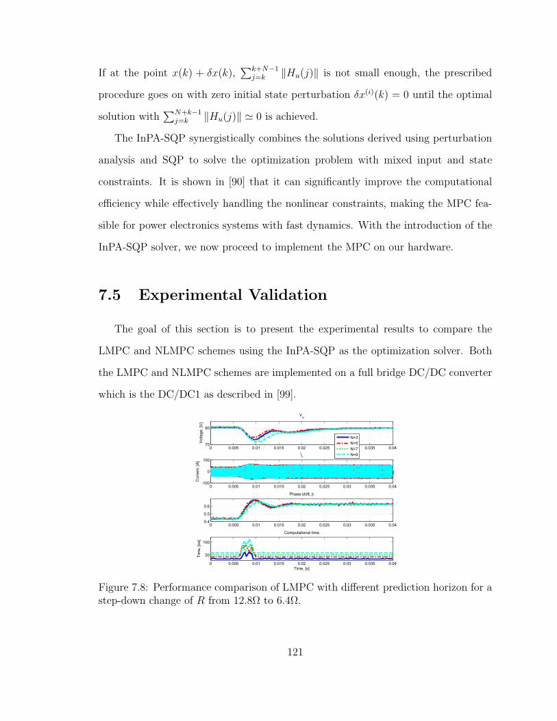
If at the point x(k) + δx(k),∑k+N−1
j=k ‖Hu(j)‖ is not small enough, the prescribed
procedure goes on with zero initial state perturbation δx(i)(k) = 0 until the optimal
solution with∑N+k−1
j=k ‖Hu(j)‖ ' 0 is achieved.
The InPA-SQP synergistically combines the solutions derived using perturbation
analysis and SQP to solve the optimization problem with mixed input and state
constraints. It is shown in [90] that it can significantly improve the computational
efficiency while effectively handling the nonlinear constraints, making the MPC fea-
sible for power electronics systems with fast dynamics. With the introduction of the
InPA-SQP solver, we now proceed to implement the MPC on our hardware.
7.5 Experimental Validation
The goal of this section is to present the experimental results to compare the
LMPC and NLMPC schemes using the InPA-SQP as the optimization solver. Both
the LMPC and NLMPC schemes are implemented on a full bridge DC/DC converter
which is the DC/DC1 as described in [99].
0 0.005 0.01 0.015 0.02 0.025 0.03 0.035 0.0475
80
Vo
Vol
tage
, [V
]
N=3N=5N=7N=9
0 0.005 0.01 0.015 0.02 0.025 0.03 0.035 0.04-100
0
100iL
Cur
rent
, [A
]
0 0.005 0.01 0.015 0.02 0.025 0.03 0.035 0.040.4
0.5
0.6
Phase shift, β
0 0.005 0.01 0.015 0.02 0.025 0.03 0.035 0.04
50
100
Computational time
Tim
e, [u
s]
Time, [s]
Figure 7.8: Performance comparison of LMPC with different prediction horizon for astep-down change of R from 12.8Ω to 6.4Ω.
121
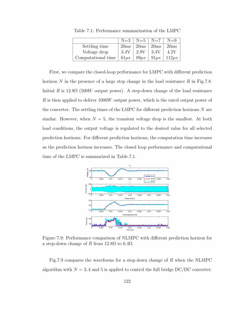
Table 7.1: Performance summarization of the LMPC
N=3 N=5 N=7 N=9Settling time 20ms 20ms 20ms 20msVoltage drop 3.4V 2.9V 3.4V 4.2V
Computational time 61µs 89µs 91µs 112µs
First, we compare the closed-loop performance for LMPC with different prediction
horizon N in the presence of a large step change in the load resistance R in Fig.7.8.
Initial R is 12.8Ω (500W output power). A step-down change of the load resistance
R is then applied to deliver 1000W output power, which is the rated output power of
the converter. The settling times of the LMPC for different prediction horizons N are
similar. However, when N = 5, the transient voltage drop is the smallest. At both
load conditions, the output voltage is regulated to the desired value for all selected
prediction horizons. For different prediction horizons, the computation time increases
as the prediction horizon increases. The closed loop performance and computational
time of the LMPC is summarized in Table.7.1.
0 0.005 0.01 0.015 0.02 0.025 0.03 0.035 0.0475
80
Vo
Vol
tage
, [V
]
0 0.005 0.01 0.015 0.02 0.025 0.03 0.035 0.04-100
0
100iL
Cur
rent
, [A
]
0 0.005 0.01 0.015 0.02 0.025 0.03 0.035 0.040.4
0.6
0.8Phase shift, β
0 0.005 0.01 0.015 0.02 0.025 0.03 0.035 0.04
50
100
Computational time
Tim
e, [u
s]
Time, [s]
N=3N=4N=5
Figure 7.9: Performance comparison of NLMPC with different prediction horizon fora step-down change of R from 12.8Ω to 6.4Ω.
Fig.7.9 compares the waveforms for a step-down change of R when the NLMPC
algorithm with N = 3, 4 and 5 is applied to control the full bridge DC/DC converter.
122

Table 7.2: Performance summarization of the NLMPC
N=3 N=4 N=5Settling time 13ms 13ms 13msVoltage drop 3.9V 3.9V 3.9V
Computational time 102µs 105µs 113µs
A step-down change of the load resistance R from 12.8Ω to 6.4Ω is then applied to
deliver 1000W rated output power. At both load conditions, the output voltage is
regulated to the desired value for all selected prediction horizon. The performance
of NLMPC for N = 3, 4 and 5 are essentially the same while the computation time
increases as the prediction horizon increases. Therefore, it is desirable to choose
N = 3 to reduce computation time. The closed loop performance and computational
time of the NLMPC is summarized in Table.7.2.
0 0.005 0.01 0.015 0.02 0.025 0.030
50
Vo
Vol
tage
, [V
]
0 0.005 0.01 0.015 0.02 0.025 0.03-100
0
100iL
Cur
rent
, [A
]
0 0.005 0.01 0.015 0.02 0.025 0.03
0.5
1Phase shift, β
0 0.005 0.01 0.015 0.02 0.025 0.03
50
100
150Computational time
Tim
e, [u
s]
Time, [s]
NLMPC with N=3LMPC with N=5
Figure 7.10: Comparison of the LMPC and NLMPC schemes during the startingprocess.
Fig.7.10 shows the experimental waveforms of LMPC and NLMPC of the full
bridge DC/DC converter during the starting process with rated 1KW load. For both
the LMPC and NLMPC schemes, the peak currents are limited within the maximum
tolerable value 75A although the peak current is slightly higher than 75A during the
first 300µs. The maximum output voltage is 86V for the LMPC scheme while, for the
123

NLMPC scheme, it is 81.2V. The maximum computation time for the LMPC scheme
is 128µs which is 40µs longer than the NLMPC scheme’s 88µs.
0 0.005 0.01 0.015 0.02 0.025 0.03 0.035 0.0476
78
80
82
Vo
Vol
tage
, [V
]
0 0.005 0.01 0.015 0.02 0.025 0.03 0.035 0.04
-50
0
50
iL
Cur
rent
, [A
]
0 0.005 0.01 0.015 0.02 0.025 0.03 0.035 0.040.4
0.6
0.8Phase shift, β
0 0.005 0.01 0.015 0.02 0.025 0.03 0.035 0.0420406080
100120
Computational time
Tim
e, [u
s]
Time, [s]
NLMPC with N=3LMPC with N=5
Figure 7.11: Comparison of the LMPC and NLMPC schemes for a step-down changeof R from 12.8Ω to 6.4Ω.
Fig.7.11 shows the waveforms of LMPC and NLMPC of the full bridge DC/DC
converter under a step-down change of R. The LMPC scheme has N = 5 while
the NLMPC scheme has N = 3. We define the voltage regulation error as ev =∫ 0.04
0|Vo − 80| dt. For the LMPC scheme, ev = 0.025 while, for the NLMPC scheme,
ev = 0.023. Moreover, from Fig.7.11, the settling time of the NLMPC scheme is
shorter than that of the LMPC scheme. However, the maximum voltage drop of the
LMPC scheme is 2.8V which is 1.1V lower than that of the NLMPC scheme. The
maximum computation time for the LMPC scheme is 89µs while that of the NLMPC
scheme is 104µs.
Finally, Fig.7.12 shows the experimental waveforms for LMPC and NLMPC of
the full bridge DC/DC converter under the overload operation condition. The power
converter is initially operating with 1KW load (R = 6.4Ω). The load resistance R
is then reduced to 2Ω. For both the LMPC and NLMPC schemes, the responses are
similar. At the steady state after the transient, the peak current is limited within
124

0 0.005 0.01 0.015 0.02 0.025 0.03 0.035 0.0440
60
80
Vo
Vol
tage
, [V
]
0 0.005 0.01 0.015 0.02 0.025 0.03 0.035 0.04-100
0
100iL
Cur
rent
, [A
]
0 0.005 0.01 0.015 0.02 0.025 0.03 0.035 0.04
0.5
1Phase shift, β
0 0.005 0.01 0.015 0.02 0.025 0.03 0.035 0.0420
40
60
80Computational time
Tim
e, [u
s]
Time, [s]
NLMPC with N=3LMPC with N=5
Figure 7.12: Comparison of the LMPC and NLMPC schemes under overload opera-tion condition.
the maximum tolerable value 75A except that the peak current is slightly higher than
75A during the transient. This is partially due to the fact that we do not use a current
sensor in the control schemes. The output voltage drops from 80V to 40V during the
transient since iL1 is constrained. The maximum computation time for the LMPC
scheme is 69µs which is 6µs shorter than that of the NLMPC scheme.
7.6 Summary
In this chapter, the LMPC and NLMPC schemes are proposed to control a FBC
of the DHPS. The control objective is to regulate the output voltage without vio-
lating the peak current constraint. A linear or a nonlinear dynamic model is used
for future behavior prediction while the peak current protection requirement was
formulated as a mixed input and state constraint for both the MPC schemes. The
computation time and closed loop system performances for the LMPC and NLMPC
of the FBC under three operating conditions are compared. The InPA-SQP method
is employed to solve the nonlinearly constrained optimal control problems with a
125

sub-millisecond level sampling time. The experimental results reveal that both the
LMPC and NLMPC schemes successfully achieved voltage regulation and peak cur-
rent protection. In comparison with the LMPC scheme, the NLMPC scheme achieves
better performance during the starting process and load step-change process and has
the similar performance under the overload operation condition. In terms of compu-
tation time, the LMPC scheme has slightly shorter one during the load step-change
process and overload operation condition. However, the NLMPC scheme has a much
shorter computation time than the LMPC scheme during the starting process. In
addition, the implementation of the LMPC scheme requires an offset-free algorithm
to eliminate the steady state error, complicating the control design. Therefore, con-
sidering the algorithm complexity, the closed loop performance and the necessary
computation time, the NLMPC scheme is more desirable than the LMPC scheme for
this application.
126

Chapter 8
Conclusions and Future Work
This dissertation has focused on the modeling, analysis, and control of a DC hy-
brid power system with multiple power converters, aiming at all electric ship as the
application platform. At the system level, tools are developed to facilitate the re-
search described in this dissertation, including the DHPS testbed (Chapter 2) and
the IPS model of an AES (covered in Chapter 3). At the device level, in-depth
analysis and design are performed for DC/DC converters which will serve as the crit-
ical enablers for the DHPS power management system. New modulation strategy is
also developed to overcome the low efficiency of conventional PSM. Advanced control
methodology, namely the model predictive control, is implemented for the full bridge
DC/DC converter to handle physical constraints and achieve voltage regulation ob-
jective (Chapter 7).
8.1 Conclusions
The main work and results of this dissertation are summarized as follows:
• Developed a testbed for DC hybrid power system
In Chapter 2, a DC hybrid power system testbed is introduced. The testbed
127

includes a realtime simulation and control rapid prototyping platform, three iso-
lated DC/DC converters, two programmable power sources, two programmable
electronics loads, and a supercapacitor based energy storage bank. This testbed
has: (1) fully digital simulation capability as a preliminary analysis tool to
support the modeling and control development effort, (2) adequate hardware
resources for controlling complex dynamic system, (3) necessary hardware, in-
cluding power sources, power converters and loads, to verify analysis, modeling
and evaluation results, and (4) control rapid prototyping capability to ensure
quick implementation of advanced control algorithms for system performance
evaluation and design validation. Therefore, this testbed can facilitate opti-
mization and power management strategy development for the DHPS.
• Developed a modularized simulation model for the IPS of an AES
The IPS model has power generation modules including a gas turbine and
fuel cell, an electric propulsion module and a zonal electric distribution system
which, by itself, has many power conversion modules. The simulation results
verify that the IPS model can be used to perform simulations for scenarios such
as failure emulation, power flow path reconfiguration and energy management.
This model provides an effective tool for AES system research.
• Designed a new power flow model for the dual active bridge DC/DC converter
In addition to those major parameters used by conventional power flow analysis,
this new model also considers minor parameters, namely the power semiconduc-
tor voltage loss and dead time. The minor parameters are critical for explaining
the observed internal power transfer and phase drift phenomena, which are rele-
vant to power flow characterization of the DAB converter. While the new model
provides a more accurate prediction over a wide range of operating conditions,
128

it also identifies new characteristics such as reverse power transfer and energy
sink that are observed in experiments. Therefore, the new model can serve as a
research tool for optimal hardware design, operating range selection and power
management strategy development.
• Proposed a novel current mode PWM strategy for the dual active bridge DC/DC
converter
The proposed modulation strategy can avoid the drawbacks of the conventional
phase shift modulation and achieve: (1) zero circulating current to reduce con-
duction loss; (2) soft-switching over the full operating range to reduce switch-
ing loss; (3) zero idling power to eliminate idle loss; (4) simple but accurate
power flow characterization; and (5) controllable output power between zero
and the maximum for different combinations of terminal voltages. Moreover,
the proposed modulation strategy enables the converter to achieve the same
power density under the same current stress as that of a phase shift modulated
converter. Therefore, in comparison with the traditional ones, the proposed
strategy is more suitable for energy storage system application.
• Developed and implemented LMPC and NLMPC for a full bridge DC/DC con-
verter
Both the LMPC and NLMPC schemes are employed to control the full bridge
DC/DC converter. The controllers can successfully regulate the output voltage
without violating the peak current constraint. Moreover, comparative evalua-
tion of the LMPC and NLMPC schemes is performed. The computation time
and closed loop system performances under starting, overload and load step
change conditions are compared. The experimental results reveal that both the
LMPC and NLMPC schemes can successfully achieve voltage regulation and
129

peak current protection. Considering the algorithm complexity, the closed loop
performance and the necessary computation time, the NLMPC scheme is more
desirable than the LMPC for this application. This is the first implicit MPC
application for power electronics system with very fast dynamics.
8.2 Future Work
Although substantial progress has been made on the modeling, analysis, optimiza-
tion, and control of the DC hybrid power system, the results of this dissertation point
to several interesting directions for future work.
• Investigating control methodologies for power converters with multiple operating
modes
Our testbed has two full bridge DC/DC converters. The full bridge DC/DC
converter can operate with either a discontinuous conduction mode or a contin-
uous conduction mode. In this dissertation, we developed a dynamic model and
designed the MPC schemes for the full bridge DC/DC converter based on the
assumption that it operates with a discontinuous conduction mode. Although
we designed the converter to operate with a discontinuous conduction mode to
eliminate the negative current, the converter could operate with a continuous
conduction mode under certain conditions. Therefore, we could use the hybrid
control scheme for the power converters to ensure the closed loop performance
if the power converter operates with multiple modes.
• Exploring advanced control methodologies for the DC hybrid power system
In this dissertation, we employed LMPC and NLMPC schemes to control the
full bridge DC/DC converter in Chapter 7. The DC hybrid power system in-
vestigated in this dissertation has multiple power converters. It is a challenging
130

control problem to coordinate the power converters to achieve fast power track-
ing without violating the physical limitations of the power converters. There-
fore, development of an efficient strategy for the coordination of decentralized
MPC schemes could be an opportunity and a challenge in enhancing the system
level control performance.
131

Appendix
132

Appendix A
Gas Turbine Model
The turbine model is based on [102]. For a self contained presentation, we include
the key equations in this appendix.
The compressor mass flow is given by
Wc =
√Tambpamb
φc
The mass flow parameter φc is a function of the corrected speed parameter ωtc (=
ωtc√Tc,in
) and pressure ratio across the compressor ΓPR,c. This is determined using zero
slope line method ( [103]) and is given by
φcφZS,c
=
1 + kc2
1− ekc1
(ΓPR,c
ΓZSPR,c
−1
) , (ΓPR,c < ΓZSPR,c)
1− kc2kc1(
ΓPR,cΓZSPR,c
− 1), (ΓPR,c ≥ ΓZSPR,c)
where φZS,c, ΓZS,c are zero slope mass flow parameter and pressure ratio respectively.
These along with the constants kc1 and kc2 are polynomial functions of ωtc, whose
coefficients are determined by regression on the compressor maps.
133

The compressor isentropic efficiency is given by
ηis,c = kc3φ2c + kc4φc + kc5
where kc3, kc4, kc5 are quadratic functions of the speed parameter ωtc whose coefficients
are determined by regression on the compressor efficiency maps.
The turbine mass flow (Wt) is given by
Wt =
√Tbpb
φt
ΓPR,t is the pressure ratio across the turbine. The function φt depends on the turbine
expansion ratio ΓPR,t, corrected speed parameter ωtc and is given by
φt =
At
√2γγ−1
(Γ
2γ
PR,t − Γγ+1γ
PR,t
), (ΓPR,t > pcrit)
At
√2γγ−1
(p
2γ
crit − pγ+1γ
crit
), (ΓPR,t ≤ pcrit)
where At is the effective flow area and is given by
At =kt1
Γ2PR,t
+kt2
ΓPR,t+ kt3.
The coefficients kt1, kt2 and kt3 are polynomial functions of the corrected speed pa-
rameter ωtc and is determined using regression on the turbine maps.
The turbine isentropic efficiency is given by
ηis,t = kt4Γ2PR,t + kt5ΓPR,t + kt6
where kt4, kt5, kt6 are cubic functions of the speed parameter ωtc whose coefficients
134

are determined by regression on the turbine efficiency maps.
135

Bibliography
136

Bibliography
[1] N. Doerry and J. C. Davis, “Integrated power system for marine applications,”
Naval Engineers Journal, 1994.
[2] N. Doerry, H. Robey, J. Amy and C. Petry, “Power the future with the integrated
power system,” Naval Engineers Journal, 1996.
[3] C. Petry and J. Rumburg, “Zonal electrical distribution systems: an affordable
architecture for the future,” Naval Engineers Journal, 1993.
[4] J. G. Ciezki and R. W. Ashton, “Selection and stability issues associated with
a navy shipboard DC zonal electric distribution system,” IEEE Transactions on
Power Delivery, 2000.
[5] T. Ericsen and A. Tucker, “Power electronics building blocks and potential power
modulator applications,” IEEE Conference Record of the Twenty-Third Interna-
tional Power Modulator Symposium, New York, 1998.
[6] Z. Ye, K. Xing, S. Mazumder, D. Borojevic and F.C. Lee, “Modeling and control of
parallel three-phase PWM boost rectifiers in PEBB-based DC distributed power
systems,” IEEE Applied Power Electronics Conference, 1998.
[7] C. Dufour and J. Belanger, “A PC-based real-time parallel simulator of electric
systems and drives,” International Conference on Parallel Computing in Electrical
Engineering, 2004.
[8] P. Moraal and I. Kolmanovsky, “Turbocharger modeling for automotive control
applications,” Journal of Engg. For Gas Turbines and Power, 2003.
137
[9] V. Tsourapas, J. Sun and A. Nickens, “Control oriented modeling and analysis of
a hybrid solid oxide fuel cell and gas turbine (SOFC/GT) system,” Proceedings
of the 2006 Fuel Cell Seminar, 2006.
[10] E. A. Lewis, “Cyclo convertor drive systems,” Sixth International Conference on
Power Electronics and Variable Speed Drives, 1996.
[11] D. Fu, F. C. Lee, “Phase compensation driving scheme for SR,” Patent Applica-
tion No:11/749,405
[12] D. Fu, F. C. Lee, Y. Liu, and M. Xu, “Multi-element resonant converters,” Patent
Application No.:12/134,413
[13] D. Fu, F. C. Lee, Y. Qiu, F. Wang, “A novel high-power-density three-level LCC
resonant converter with constant-power-factor-control for charging applications,”
IEEE Transaction on Power Electronics, 2008.
[14] P. Tenti, L. Malesani and L. Rossetto, “Optimum control of N-input K-output
matrix converters,” IEEE Transactions on Power Electronics, 1992.
[15] S. S. Kalsi, B. B. Gamble, G. Snitchler and S. O. Ige, “The status of HTS
ship propulsion motor developments,” IEEE Power Engineering Society General
Meeting, 2006
[16] T. I. Fossen, Marine Control Systems: Guidance, Navigation and Control of
Ships, Rigs and Underwater Vehicles, Marine Cybernetics AS, 2002.
[17] D. Fu, Y. Liu, F. C. Lee, M. Xu, “A novel driving scheme for synchronous recti-
fiers (SR) for LLC resonant converters,” IEEE Transaction on Power Electronics,
2009.
[18] D. Huang, D. Fu, F. C. Lee, “High switching frequency, high efficiency CLL
resonant converter with synchronous rectifier,” in Proc. IEEE ECCE, 2009.
[19] D. Fu, F. C. Lee, Y. Liu, M. Xu, “Novel multi-element resonant converters for
front-end DC/DC converters,” in Proc. IEEE PESC 2008.
138

[20] R. C. Bansal, “Automatic reactive power control of isolated wind-diesel hybrid
power systems,” IEEE Trans. Industrial Electronics, vol. 53, pp.1116-1126, Jun.
2006.
[21] T. Senjyu, T. Nakaji, K. Uezato and T. Funabashi,“A hybrid power system using
alternative energy facilities in isolated island,” IEEE Trans. Energy Conversion,
vol. 20, pp.406-414, Jun. 2005.
[22] V. Tsourapas, A. Stefanopoulou, and J. Sun, “Model-based control of an inte-
grated fuel cell and fuel processor with exhaust heat recirculation,” IEEE Trans.
on Control Systems Technology, vol. 15, pp.233-245, Mar. 2007.
[23] A. T-Raissi and D. L. Block, “Hydrogen: automotive fuel of the future,” IEEE
Power and Energy Magazine, vol. 2, pp.40-45, Nov./Dec. 2004.
[24] D. Fu, B. Lu, F. C. Lee, “1MHz high efficiency LLC resonant converters with
synchronous rectifier,” in Proc. IEEE PESC, 2007.
[25] D. Fu, Y. Qiu, Y. Sun, F. C. Lee, “A 700kHz high-efficiency high-power-density
three-level parallel resonant DC-DC converter for high-voltage charging applica-
tions,” in Proc. IEEE APEC, 2007.
[26] Y. Qiu, B. Lu, B. Yang, D. Fu, F. C. Lee, “A high-frequency high-efficiency
three-level LCC converter for high-voltage charging applications,” in Proc. IEEE
PESC, 2004.
[27] W. Gao,“Performance comparison of a fuel cell-battery hybrid powertrain and
a fuel cell-ultracapacitor hybrid powertrain,” IEEE Trans. Vehicular Technology,
vol. 54, pp.846-855, May 2005.
[28] A. Emadi, S. S. Williamson and A. Khaligh,“Power electronics intensive solutions
for advanced electric, hybrid electric, and fuel cell vehicular power systems,” IEEE
Trans. Power Electronics, vol. 21, pp.567-577, May 2006.
139
[29] X. Zhang, C. Mi, A. Masrur, and D. Daniszewski, “Wavelet based power man-
agement of hybrid electric vehicles with multiple onboard power sources,” Journal
of Power Sources, vol. 185, pp. 1533-1543, Dec. 2008.
[30] H. Sheng, W. Shen, H. Wang, D. Fu, Y. Pei, “Design and implementation of
high power density three-level parallel resonant converter for capacitor charger,”
in Proc. IEEE APEC, 2007.
[31] D. Fu, Y. Qiu, B. Lu, F. Wang, F. C. Lee, “An improved three-level LCC
converter with a novel control strategy for high-frequency high-power-density
capacitor-charging power supplies,” in Proc. IEEE APEC, 2006.
[32] H. Bai, and C. Mi, “Eliminate reactive power and increase system efficiency of
isolated bidirectional dual-active-bridge dc-dc converters using novel dual-phase-
shift control,” IEEE Trans. Power Electronics, vol.23, pp.2905-2914, Nov. 2008.
[33] J. Sun, D. M. Mitchell, M. F. Greuel, P. T. Krein, and R. M. Bass, “Averaged
modeling of PWM converters operating in discontinuousconduction mode,” IEEE
Trans. Power Electronics, vol. 16, pp.482-492, Jul. 2001.
[34] R. Morrison, and M. G. Egan, “A new power-factor-corrected single-transformer
UPS design,” IEEE Trans. Industry Applications, vol.36, pp.171-179, Jan./Feb.
2000.
[35] F. Krismer, J. Biela, and J. W. Kolar, “A comparative evaluation of isolated bi-
directional dc/dc converters with wide input and output voltage range,” in Proc.
Industrial Applications Society Annual Meeting, 2005, pp.599-606.
[36] F. Krismer, J. Biela, and J. W. Kolar, “Performance optimization of a high
current dual active bridge with a wide operating voltage range,” in Proc. IEEE
Power Electronics Specialists Conf. (PESC), 2006, pp.1-7.
[37] J. L. Duarte, M. Hendrix, and M. G. Simoes, “Three-port bidirectional converter
for hybrid fuel cell systems,” IEEE Trans. Power Electronics, vol.22, pp.480-487,
Mar. 2007.
140
[38] H. M. Tao, A. Kotsopoulos, J.L. Duarte, and M.A.M. Hendrix, “Transformer-
coupled multiport ZVS bidirectional dc-dc converter with wide input range,” IEEE
Trans. Power Electronics, vol.23, pp.771-781, Mar. 2008.
[39] J. Walter, and R. W. De Doncker, “High-power galvanically isolated dc/dc con-
verter topology for future automobiles”, in Proc. IEEE Power Electronics Spe-
cialists Conf. (PESC), 2003, pp.27-32.
[40] D. Fu, P. Kong, S. Wang, F. C. Lee, M. Xu, “Analysis and suppression of
conducted EMI eEmissions for front-end LLC resonant DC/DC converters,” in
Proc. IEEE PESC, 2008.
[41] D. Fu, Y. Liu, F. C. Lee, M. Xu, “An improved novel driving scheme of syn-
chronous rectifiers for LLC resonant converters,” in Proc. IEEE APEC, 2008.
[42] F. C. Lee, S. Wang, P. Kong, C. Wang, D. Fu, “Power architecture design with
improved system efficiency, EMI and power density,” in Proc. IEEE PESC, 2008.
[43] H. Sangtaek, and D. Divan,“Bi-directional dc/dc converters for plug-in hybrid
electric vehicle (PHEV) applications,” in Proc. IEEE Appl. Power Electron. Conf.
Expo (APEC), 2008, pp.1-5.
[44] C. Zhao, S. D. Round, and J. W. Kolar, “An isolated three-port bidirectional
dc-dc converter with decoupled power flow management,” IEEE Trans. Power
Electron., vol.23, pp.2443-2453, Sept. 2008.
[45] H. Bai, C. Mi, and S. Gargies, “The short-time-scale transient processes in
high-voltage and high-power isolated bidirectional dc-dc converters,” IEEE Trans.
Power Electron., vol.23, pp.2648-2656, Nov. 2008.
[46] S. Inoue, and H. Akagi, “A bidirectional dc-dc converter for an energy storage
system with galvanic isolation,” IEEE Trans. Power Electron., vol.22, pp.2299-
2306, Nov. 2007.
141
[47] S. Inoue, and H. Akagi, “A bidirectional isolated dc-dc converter as a core circuit
of the next-generation medium-voltage power conversion system,” IEEE Trans.
Power Electronics, vol.22, pp.535-542, Mar. 2007.
[48] N. M. L. Tan, S. Inoue, A. Kobayashi, and H. Akagi, “Voltage balancing of a 320-
V, 12-F electric double-layer capacitor bank combined with a 10-kW bidirectional
isolated dc-dc converter,” IEEE Trans. Power Electronics, vol.23, pp.2755-2765,
Nov. 2008.
[49] F. Z. Peng, H. Li, G.-J. Su, and J. S. Lawler, “A new ZVS bi-directional dc-dc
converter for fuel cell and battery application,” IEEE Trans. Power Electronics,
vol. 19, pp.54-65, Jan. 2004.
[50] H. Xiao, and S. Xie, “A ZVS bidirectional dc-dc converter with phase-shift plus
PWM control scheme,” IEEE Trans. Power Electronics, vol. 23, pp. 813-823, Mar.
2008.
[51] J. Zhang, F. Zhang, X. Xie, D. Jiao, and Z. Qian, “A novel ZVS DC/DC con-
verter for high power applications,” IEEE Trans. Power Electronics, vol. 19, pp.
420-429, Mar. 2004.
[52] H. Zhou, and A. M. Khambadkone, “Hybrid modulation for dual active bridge bi-
directional converter with extended power range for ultracapacitor application”,
in Proc. Industry Applications Society Annual Meeting (IAS), 2008, pp.1-8.
[53] A. K. Jain, and R. Ayyanar, “PWM control of dual active bridge: comprehensive
analysis and experimental verification”, in Proc. Annual Conference of the IEEE
Industry Electronics Society (IECON), 2008, pp.909-915.
[54] R. W. De Doneker, D. M. Divan, and M. H. Kheraluwala, “A three-phase soft-
switched high-power-density dc/dc converter for high-power applications,” IEEE
Trans. Industry Applications, vol. 27, pp.797-806, Jan./Feb. 1991.
142
[55] M. H. Kheraluwala, R. W. Gascoigne, D.M. Divan, and E. D. Baumann, “Per-
formance characterization of a high-power dual active bridge dc-to-dc converter,”
IEEE Trans. Industry Applications, vol. 28, pp.1294-1301, Nov./Dec. 1992.
[56] F. Z. Peng, H. Li, G.-J. Su, and J. S. Lawler, “A new ZVS bi-directional dc-dc
converter for fuel cell and battery application,” IEEE Trans. Power Electronics,
vol. 19, pp.54-65, Jan. 2004.
[57] D. H. Xu, C. H. Zhao, and H. F. Fan,“ A PWM plus phase-shift control bidi-
rectional dc-dc converter,” IEEE Trans. Power Electronics, vol. 19, pp.666-675,
May 2004.
[58] L. Zhu, “A novel soft-commutating isolated boost full-bridge ZVS-PWM dc-dc
converter for bi-directional high power applications,” IEEE Trans. Power Elec-
tronics, vol. 21, pp.422-429, Mar. 2006.
[59] H.-J. Chiu, and L.-W. Lin, “A bidirectional dc-dc converter for fuel cell electric
vehicle driving system,” IEEE Trans. Power Electronics, vol. 21, pp. 950-958, Jul.
2006.
[60] J. Zhang, J.-S. Lai, R.-Y. Kim, and W. Yu, “High-power density design of a soft-
switching high-power bidirectional dc-dc converter,” IEEE Trans. Power Electron-
ics, vol. 22, pp. 1145-1153, Jul. 2007.
[61] R.-J. Wai, and R.-Y. Duan, “High-efficiency bidirectional converter for power
sources with great voltage diversity,” IEEE Trans. Power Electronics, vol. 22, pp.
1986-1996, Sept. 2007.
[62] H. Xiao, and S. Xie, “A ZVS bidirectional dc-dc converter with phase-shift plus
PWM control scheme,” IEEE Trans. Power Electronics, vol. 23, pp. 813-823, Mar.
2008.
[63] H. Sheng, D. Fu, X. Yang, F. Wang, F. C. Lee, “Comparison of ZVS operation
modes with and without phase shift for three-level resonant converters,” in Proc.
IEEE APEC, 2006.
143
[64] D. Fu, “Improved resonant converters with a novel control strategy for high-
voltage pulsed power supplies,” Master’s thesis, Virginia Polytechnic Institute
and State University, 2004.
[65] R. W. Erickson, and D. Maksimovic, Fundamentals of Power Electronics, Second
Edition, Norwell, Mass.: Kluwer Academic, 2001.
[66] L. Chen, and F. Z. Peng, “Dead-time elimination for voltage source inverters,”
IEEE Trans. Power Electronics, vol.23, pp.574-580, Mar. 2008.
[67] G. Seenumani, J. Sun, and H. Peng, “Real-time Power Management of Integrated
Power Systems in All Electric Ships Using Time Scale Separation,” submitted to
IEEE Transactions On Control System Technology, 2009.
[68] G. Seenumani, J. Sun, and H. Peng, “Exploiting Time Scale Separation For
Efficient Real-Time Optimization Of Integrated Shipboard Power Systems,” in
Proc. ASME Dynamic Systems and Control Conference, 2008.
[69] G. Seenumani, J. Sun and H. Peng, “A Numerically Efficient Iterative Procedure
for Hybrid Power System Optimization Using Sensitivity Functions,” in Proc.
American Control Conference, 2007.
[70] S. Chattopadhyay and S. Das, “A digital current-mode control technique for
DC-DC converters,” IEEE Trans. Power Electronics, vol. 21, pp.1718-1726, Nov.
2006.
[71] M. Chen, A. Mathew, and J. Sun, “Nonlinear current control of single-phase
PFC converters,” IEEE Trans. Power Electronics, vol. 18, pp.2187-2194, Nov.
2007.
[72] Y. Lu, K. W. E. Cheng, and S. L. Ho, “Quasi current mode control for the
phase-shifted series resonant converter,” IEEE Trans. Power Electronics, vol. 23,
pp.353-358, Jan. 2008.
144
[73] J. Sun and M. Chen, “Nonlinear average current control using partial current
measurement,” IEEE Trans. Power Electronics, vol. 23, pp.1641-1648, Jul. 2008.
[74] R. Redl and I. Novak, “Instabilities in current-mode controlled switching voltage
regulators,” in Proc. IEEE Power Electronics Specialists Conf. (PESC), 1981,
pp.17-28.
[75] S. Kouro, P. Cortes, R. Vargas, U. Ammann, and J. Rodriguez, “Model predic-
tive control-a simple and powerful method to control power converters,” in IEEE
Trans. Industrial Electronics, vol. 56, pp.1826-1838, Jun. 2009.
[76] T. Geyer, G. Papafotiou, and M. Morari, “Model predictive direct torque control-
part I: concept, algorithm, and analysis,” in IEEE Trans. Industrial Electronics,
vol. 56, pp.1894-1905, Jun. 2009.
[77] T. Geyer, G. Papafotiou, and M. Morari, “Model predictive direct torque control-
part II: implementation and experimental evaluation,” in IEEE Trans. Industrial
Electronics, vol. 56, pp.1906-1915, Jun. 2009.
[78] E. I. Silva, B. P. McGrath, D. E. Quevedo, and G. C. Goodwin, “Predictive
control of a flying capacitor converter,” in Proc. American Control Conference,
2007, pp.3763-3768.
[79] S. Qin and T. Badgwell, “A survey of industrial model predictive control tech-
nology,” Control engineering practice, vol. 11, pp.733-764, 2003.
[80] D. Q. Mayne, J. B. Rawlings, C. V. Rao, and P. O. M. Scokaert, “Constrained
model predictive control: stability and optimality,” Automatica, vol. 36, pp.789-
814, Jun. 2000.
[81] M. Morari and J. Lee, “Model predictive control: past, present and future,”
Computers and Chemical Engineering, vol. 23, pp.667-682, 1999.
145

[82] G. Pannocchia, and A. Bemporad, “Combined design of disturbance model and
observer for offset-free model predictive control,” IEEE Trans. Automatic Control,
vol. 52, pp.1048-1053, Jun. 2007.
[83] F. Borrelli, and M. Morari, “Offset free model predictive control,” in Proc. IEEE
Conference on Decision and Control, 2007, pp.1245-1250.
[84] V. L. Bageshwar, and F. Borrelli, “Observer pole placement limitations for a class
of offset-free model predictive controllers,” in Proc. American Control Conference,
2008, pp.447-452.
[85] G. Pannocchia and J. B. Rawlings, “Disturbance models for offset-free MPC
control,” AIChE Journal, vol. 49, pp.426-437, 2002.
[86] A. Bemporad, M. Morari, V. Dua, and E. N. Pistikopoulos, “The explicit linear
quadratic regulator for constrained systems,” Automatica, vol. 38, pp.3-20, Jan.
2002.
[87] P. T∅ndel, T. A. Johansen, and A. Bemporad, “An algorithm for multi-
parametric quadratic programming and explicit MPC solutions,” Automatica, vol.
39, pp.489-497, Mar. 2003.
[88] T. Geyer, G. Papafotiou, and M. Morari, “Hybrid model predictive control of
the step-down DC-DC converter,” IEEE Trans. Control Systems Technology, vol.
16, pp.1112-1124, Nov. 2008.
[89] Y. Wang and S. Boyd, “Fast model predictive control using online optimization,”
in Proc. of the 17th IFAC World Congress, 2008, pp.6974-6997.
[90] R. Ghaemi, J. Sun, and I. Kolmanovsky, “An integrated perturbation analysis
and sequential quadratic programming approach for model predictive control,”
Automatica, vol. 45, pp. 2412-2418, Sep. 2009.
146

[91] R. Ghaemi, J. Sun, and I. Kolmanovsky, “Neighbering extremal solution for
nonlinear dicrete-time optimal control problems with state inequality constraints,”
IEEE Trans. Automatic Control, vol. 54, 2009.
[92] Y. Xie, G. Seenumani, and J. Sun, “Real-time simulation and optimization of
multi-scale shipboard power systems,” in Proc. Grand Challenges in Modelling
and Simulation, 2008.
[93] Y. Xie, G. Seenumani, J. Sun, Y. Liu, and Z. Li, “A PC-cluster cased real-time
simulator for all electric ship integrated power systems analysis and optimization,”
in Proc. IEEE Electric Ship Technology Symposium (ESTS), 2007.
[94] Y. Xie, J. Sun, and J. S. Freudenberg, “Power flow characterization of a bidirec-
tional galvanically isolated high power DC/DC converter over a wide operating
range,” IEEE Trans. Power Electronics, 2010.
[95] Y. Xie, J. Sun, and J. S. Freudenberg, “Development of a CM-PWM for a dual
active bridge DC/DC converter,” submitted to IEEE Transaction on Power Elec-
tronics, 2009.
[96] Y. Xie, R. Ghaemi, J. Sun, and J. S. Freudenberg, “Implicit model predictive
control of a full bridge DC/DC converter”, to appear, IEEE Trans. Power Elec-
tronics, 2009.
[97] Y. Xie, R. Ghaemi, J. Sun, and J. S. Freudenberg, “Nonlinear model predictive
control for a isolated high power full bridge DC/DC converter,” submitted to,
IEEE Trans. Control System Technology, 2010.
[98] Y. Xie, R. Ghaemi, J. Sun, and J. S. Freudenberg, “Comparative evaluation of
linear and nonlinear model predictive control for a isolated high power full bridge
DC/DC converter,” submitted to, American Control Conference (ACC’10), 2010.
[99] Y. Xie, J. Sun, C. Mi, and J. S. Freudenberg, “Analysis and modeling of a DC
hybrid power system testbed for power management strategy development,” in
Proc. IEEE Vehicle Power and Propulsion Conf. (VPPC’09), 2009.
147

[100] Y. Xie, J. Sun, and J. S. Freudenberg, “Integrated voltage regulation and
current-sensorless power tracking control for a DC hybrid power system,” in Proc.
American Control Conference (ACC’08), 2008.
[101] W. S. Levine, The control handbook, CRC Press and IEEE Press, 1996.
[102] G. G. Kulikov, and H. A. Thompson, Dynamic Modelling of Gas Turbines,
Springer.
[103] P. Moraal, and I. Kolmanovsky, “Turbocharger modeling for automotive control
applications,” Journal of Eng. For Gas Turbines and Power, 2003.
[104] C. Kong, J. Ki, and M. Kang, “A new scaling method of component maps of
Gas Turbines using system identification,” in Proc. American Control Conference,
2004.
[105] J. Kurzke, and C. Riegler, “A new compressor map scaling procedure for pre-
liminary conceptional design of gas turbines,” in Proc. ASME IGTI, 2000.
[106] J. T. Pukrushpan, A. G. Stefanopoulou, and H. Peng, Control of fuel cell power
systems, Springer.
[107] J. S. Freudenberg, A first graduate course in feedback control, 2006.
148


![[] Hybrid Self-Organizing Modeling org](https://img.pdfslide.us/doc/110x75/543c51adafaf9fe8338b4707/-hybrid-self-organizing-modeling-org.jpg)