Embed Size (px)
Citation preview

Purdue UniversityPurdue e-Pubs
Birck and NCN Publications Birck Nanotechnology Center
2-2014
Model Order Reduction for Quantum TransportSimulation of Band-To-Band Tunneling DevicesJun Z. HuangUniversity of Hong Kong, Purdue University
Lining ZhangHong Kong University of Science and Technology
Weng Cho ChewUniversity of Illinois
Guan-Hua ChenUniversity of Hong Kong
Chi-Yung YamBeijing Computational Scientific Research Center
See next page for additional authors
Follow this and additional works at: http://docs.lib.purdue.edu/nanopub
Part of the Nanoscience and Nanotechnology Commons
This document has been made available through Purdue e-Pubs, a service of the Purdue University Libraries. Please contact [email protected] foradditional information.
Huang, Jun Z.; Zhang, Lining; Chew, Weng Cho; Chen, Guan-Hua; Yam, Chi-Yung; Jiang, Li Jun; and Chan, Mansun, "Model OrderReduction for Quantum Transport Simulation of Band-To-Band Tunneling Devices" (2014). Birck and NCN Publications. Paper 1523.http://dx.doi.org/10.1109/TED.2013.2295983

AuthorsJun Z. Huang, Lining Zhang, Weng Cho Chew, Guan-Hua Chen, Chi-Yung Yam, Li Jun Jiang, and MansunChan
This article is available at Purdue e-Pubs: http://docs.lib.purdue.edu/nanopub/1523

IEEE TRANSACTIONS ON ELECTRON DEVICES, VOL. 61, NO. 2, FEBRUARY 2014 561
Model Order Reduction for Quantum TransportSimulation of Band-To-Band Tunneling Devices
Jun Z. Huang, Lining Zhang, Member, IEEE, Weng Cho Chew, Fellow, IEEE, Chi-Yung Yam,Li Jun Jiang, Senior Member, IEEE, Guan-Hua Chen, and Mansun Chan, Fellow, IEEE
Abstract— Simulations of nanoelectronic devices with nonequi-librium Green’s function are computationally very intensive, inparticular, when combined with multiband approaches, such asthe k · p methods. To reduce the cost and make the simulationof realistic devices tractable, we have developed a model orderreduction method for the simulation of hole transport in siliconnanowires using three- and six-band k · p models. It is shownin this paper that, with a spurious band elimination process,the method can be readily extended to the eight-band casethat enables us to simulate band-to-band tunneling devices.The method is demonstrated via constructing reduced modelsfor indium arsenide (InAs) nanowires and simulation of I–Vcharacteristics of InAs tunneling field-effect transistors (TFETs).The results indicate that significant model reduction can beachieved with good accuracy retained. The method is then appliedto study InAs TFETs with different channel orientations andsource-pocket TFETs with n-p-i-p doping profiles.
Index Terms— Band-to-band tunneling (BTBT), eight-bandk · p model, indium arsenide (InAs) nanowires, model orderreduction (MOR), nonequilibrium Green’s function (NEGF),source-pocket TFETs, tunneling field-effect transistors (TFETs).
I. INTRODUCTION
BAND-to-band tunneling (BTBT) is a very interestingquantum phenomenon in electronic device applications.
It accounts for a portion of the leakage current in the sub-threshold region of carbon nanotube field-effect transistors
Manuscript received September 14, 2013; revised November 20, 2013;accepted December 17, 2013. Date of current version January 20, 2014. Thiswork was supported in part by the Research Grants Council of Hong Kongunder Grant GRF 712612, Grant GRF 711511, and Grant GRF 713011, inpart by the University Grants Council of Hong Kong under Contract AoE/P-04/08, and in part by the Chinese Grant NSF 61271158. The review of thispaper was arranged by Editor A. Schenk.
J. Z. Huang was with the Department of Electrical and Electronic Engi-neering, The University of Hong Kong, Hong Kong. He is now withthe Network for Computational Nanotechnology, School of Electrical andComputer Engineering, Purdue University, West Lafayette, IN 47907 USA(e-mail: [email protected]).
L. Zhang and M. Chan are with the Department of Electronic and ComputerEngineering, The Hong Kong University of Science and Technology, HongKong (e-mail: [email protected]; [email protected]).
W. C. Chew is with the Department of Electrical and Computer Engi-neering, University of Illinois, Urbana-Champaign, IL 61801 USA (e-mail:[email protected]).
C.-Y. Yam is with the Beijing Computational Science Research Center,Beijing 100084, China (e-mail: [email protected]).
L. J. Jiang is with the Department of Electrical and Electronic Engineering,The University of Hong Kong, Hong Kong (e-mail: [email protected]).
G.-H. Chen is with the Department of Chemistry, The University of HongKong, Hong Kong (e-mail: [email protected]).
Color versions of one or more of the figures in this paper are availableonline at http://ieeexplore.ieee.org.
Digital Object Identifier 10.1109/TED.2013.2295983
(FETs) [1]. It has also been used to build novel devices,such as tunneling diodes [2] and tunneling FETs (TFETs) [3].TFETs are energy-efficient switches since their subthresholdswing (SS) can be less than 60 mV/decade at room tempera-ture [4]. This is impossible for conventional FETs, which arebased on thermal injection. Therefore, TFET has been selectedby ITRS as a very attractive candidate device for futurelow-power applications [5].
The BTBT process can be accurately simulated by com-bining nonequilibrium Green’s function (NEGF) approach [6]with tight binding [7] or eight-band k · p Hamiltonian [8]that describes both the conduction and valence bands. Unfor-tunately, these multiband NEGF studies require huge com-putational resource. To improve their efficiency, equivalentbut greatly reduced tight-binding models are constructed forsilicon nanowires (SiNWs) [9], which greatly speed up thesimulation of p-type SiNW FETs even in the presence ofinelastic scattering. For multiband k · p models, a mode spaceapproach is proposed to simulate p-type SiNW FETs andindium arsenide (InAs) TFETs [8]. However, it selects themodes only at the � point, i.e., at k = 0, which is inefficientto expand the modes that are far away from k = 0.
For three- and six-band k · p models, as is shown in [10],by sampling the Bloch modes at multiple points in thek space and (or) E space, a significantly reduced Hamiltoniancan be constructed that describes very well the valence bandtop, based on which p-type SiNW FETs are simulated withgood accuracy and efficiency. However, direct extension ofthis method to eight-band k · p model fails. The problem isthat the reduced model constructed by multipoint expansiongenerally leads to some spurious bands, in addition to thenormal bands, a situation similar to constructing the equivalenttight binding models [9] and rendering the reduced modeluseless. Therefore, it is essential to have these spurious bandseliminated, meanwhile the accuracy of the normal bands isretained.
Section II begins with a review of the eight-band k · papproach. Then, the model order reduction (MOR) methodfor the discretized NEGF equation is outlined, together withsome discussion of the discretization. The problem of spuriousbands and the procedure to eliminate them are addressed indetail. The method is validated by checking the band structuresas well as the I–V curves. The usefulness of this methodis demonstrated in Section III by simulating TFETs withdifferent crystalline orientations and with source pockets. Theconclusion is given in Section IV.
0018-9383 © 2014 IEEE. Personal use is permitted, but republication/redistribution requires IEEE permission.See http://www.ieee.org/publications_standards/publications/rights/index.html for more information.

562 IEEE TRANSACTIONS ON ELECTRON DEVICES, VOL. 61, NO. 2, FEBRUARY 2014
Fig. 1. GAA InAs TFET with n-i-p (or p-i-n) type doping profile. Thetransport direction is x . The source, channel, and drain lengths are Ls , Lg ,and Ld , respectively. Nanowire thickness is Ty and Tz . Oxide layer thicknessis denoted by To and dielectric constant is εox.
II. THEORY AND METHOD
The gate-all-around (GAA) InAs nanowire TFET to besimulated is shown in Fig. 1. The InAs nanowire is n-type(p-type) doped in the source and p-type (n-type) doped in thedrain, while it is intrinsic in the channel. The InAs nanowire issurrounded by the oxide layer, through which the gate controlsthe channel portion. The working principle of this device isbased on BTBT, as described in [3] and [4]. InAs is chosen asthe channel material because high ON-current is possible dueto its small direct bandgap and light effective masses [7].
A. Eight-Band k · p Approach
To describe the band structure involving both the conductionand valence bands of III–V compound semiconductor mate-rials, a widely used approach is the eight-band k · p model.When the eight basis functions are chosen to be spinup andspin-down s and p atomic orbital-like states, the Hamiltoniancan be written as [11], [12]
H8 (k) =[
G (k) �−�∗ G (k)∗
]. (1)
The matrix G (k) is defined as
G (k) = G1 (k) + G2 (k) + Gso (2)
where
G1 (k) =
⎛⎜⎜⎝
Eg ikx P iky P ikz P−ikx P −�/3 0 0−iky P 0 −�/3 0−ikz P 0 0 −�/3
⎞⎟⎟⎠ (3)
G2 (k) =
⎛⎜⎜⎝
Ak2 Bkykz Bkxkz Bkxky
Bkykz Mk2 + Lk2x Nkx ky Nkx kz
Bkzkx Nkx ky Mk2 + Lk2y Nkykz
Bkxky Nkx kz Nkykz Mk2 + Lk2z
⎞⎟⎟⎠(4)
and
Gso = �
3
⎛⎜⎜⎝
0 0 0 00 0 −i 00 i 0 00 0 0 0
⎞⎟⎟⎠. (5)
The matrix � is
� = �
3
⎛⎜⎜⎝
0 0 0 00 0 0 10 0 0 −i0 −1 i 0
⎞⎟⎟⎠. (6)
Here, the parameter Eg is the bandgap, � is the spin-orbitsplitoff energy, and P is proportional to the momentum matrixelement and can be evaluated by its equivalent energy E p . Theparameter A is determined from the conduction band effectivemass and B is set to be zero. L = L − M has been usedto shorten the expression. The parameters L, M , and N arerelated to the Luttinger parameters. For more discussion of theparameters, see [11] and [12].
For nanostructures, the periodicity is broken by the finitesizes and the external potentials. The wave function can befound by solving the following coupled differential equationfor envelop function Fm (m = 1, 2, . . . , 8):
8∑n=1
[H8
mn (−i∇) + V (r) δmn]Fn (r) = E Fm (r) (7)
where V (r) is the slowly varying perturbed potential distrib-ution and operator H8
mn (−i∇) is the element of H8 (k) withk replaced by the differential operator −i∇.
The parameters of bulk InAs material [11] are used in thispaper, except that the parameter E p is reduced to 18 eVaccording to [13]. Note that the adjustment of the bulk para-meters may be needed to match other band structure models,such as in [14].
B. Model Order Reduction
To solve (7) numerically with the NEGF approach, theoperator needs to be discretized first. For reasons that willbe stated later, finite-difference method (FDM) is adoptedin the transport direction, whereas k-space discretization isemployed in the transverse directions [8]. For simplicity, hardwall boundary condition is assumed at the interfaces betweenthe oxide layer and the InAs channel. The resultant matrixequation for Green’s function G (E) can be written as
[EI − H0 − � (E)] G (E) = I (8)
where H0 is the discretized k · p Hamiltonian of the isolateddevice (including the potential term) and � is the self-energymatrix due to the semi-infinite leads. For nanowire structures,such as Fig. 1, H0 can be written down layer by layer leadingto block tridiagonal form (block size Nt ).
As this equation can be large, to solve it efficiently for manydifferent energy E , a reduced-order matrix equation can beconstructed [
E I − H0 − � (E)]
G (E) = I (9)
and the reduced-order Green’s function G (E) is to be solved.Here, the reduced Hamiltonian, self-energy, and Green’s func-tion are
H0 = U†H0U, � (E) = U†� (E) U
G (E) = U†G (E) U (10)
where U is a block-diagonal unitary matrix containing thereduced basis Vi (with dimension Nt × Nm , where Nm isthe number of reduced basis) for each layer i . Then, theproblem is how to construct this transformation matrix U sothat the reduced system is as small as possible, and yet it stillaccurately describes the original system.

HUANG et al.: MOR FOR QUANTUM TRANSPORT SIMULATION 563
To construct the reduced basis Vi for layer i , the Hamil-tonian of layer i is repeated to form an infinite periodicnanowire. The reduction comes from the fact that only theelectrons near the conduction band bottom and valence bandtop are important in the transport process. To approximatethe band structure over that small region, Vi then consists ofthe Bloch modes with energy lying in that region. Multiple-point construction based on k space sampling and (or) E spacesampling can be employed [10]. Here, k space sampling isadopted since E space sampling is more costly and that theeight-band matrix is much larger than the six- or three-bandcase. Before going to the examples, there is a need to discussthe discretization because solving the Bloch modes for eachlayer is itself very costly when Nt is large.
C. Discretization
In [10], FDM is adopted and it results in extremelysparse matrices. Therefore, the Bloch modes can be obtainedefficiently with sparse matrix solvers. With shift-and-invertstrategy implemented, the Krylov subspace-based eigenvaluesolver converges very quickly, as the interested eigenvalues(close to the valence band top) distribute in a very smallarea. However, it is found that the Krylov subspace methodis less efficient in the eight-band case. The reason is that theinterested eigenvalues distribute over a larger area, as bothconduction and valence bands are of interest and between themthere is a bandgap.
Therefore, the method used in [8] is adopted. In that method,the transport direction is still discretized by FDM, whereasthe transverse directions are discretized by spectral method.Spectral method has high spectral accuracy (i.e., the errordecreases exponentially with the increase of discretizationpoints N) if the potential distribution is smooth [15]. Thisis true for devices that do not have any explicit impuritiesor surface roughness. Therefore, the Hamiltonian matrix sizeof a layer, i.e., Nt , can be kept very small (although it is lesssparse or even dense), making direct solution of the eigenvalueproblem possible. The discretized form valid for arbitrarynanowire orientation is provided in the Appendix.
D. Spurious Band Elimination
As an example, Fig. 2(a) plots the E–k dispersion foran ideal InAs nanowire orientated in the [100] direction.Fig. 2(b) shows the result using the reduced Hamiltonian H0.The reduced basis Vi (i is arbitrary here) is constructedby sampling the Bloch modes evenly in the Brillouin zone(at k = 0, ±π/4, ±2π/4, and ±3π/4 [1/nm]), with the energyE ∈ [−0.5eV, 1.7 eV], which results in Nm = 262 modes.Note that the modes at negative k can be obtained by atransformation of those at positive k [10]. Clearly, the reducedHamiltonian reproduces quite well the dispersion bands inthat energy window (except at the very bottom, which can beimproved by sampling a slightly larger energy window or morek points), demonstrating that the k space sampling is effective.However, there are also some spurious bands appearing in theconduction and valence bands, and even in the bandgap, mak-ing the reduced model useless. Moreover, different sampling
Fig. 2. E–k diagram of a 5 nm×5 nm InAs nanowire in [100] direction. Thepotential is assumed to be zero everywhere inside the nanowire. (a) Exact solu-tion. (b) Reduced model solution with spurious bands marked. (c) Reducedmodel solution with spurious bands eliminated. Only +k is shown as the bandstructure is symmetric with respect to k = 0.
points or windows would change the number and position ofthe spurious bands. This situation is not encountered in thethree- or six-band model involving only the valence bands, orin the one-band effective mass model involving the conductionband only. It should be caused by the coupling between theconduction and valence bands, which makes the eight-bandmodel indefinite. The coupling is important for materials withnarrow bandgaps.
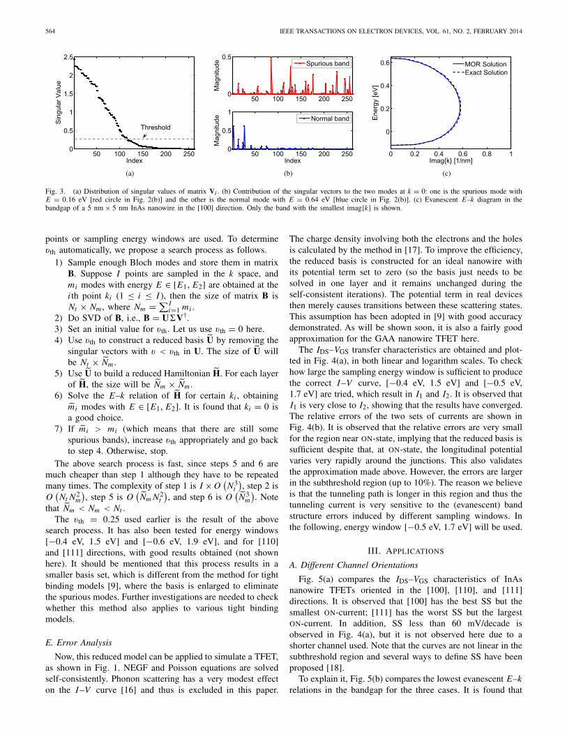
The spurious bands must be suppressed. To this end, a sin-gular value decomposition (SVD) is applied to the matrix Vi .As plotted in Fig. 3(a), the singular values spread from alarge value down to zero, suggesting there are some linearlydependent modes. These linearly dependent modes give riseto null space of the reduced model and therefore must beremoved. It is further found that the normal bands are mainlycontributed by singular vectors having large singular values,in contrast to the spurious bands where singular vectors withsmall singular values have large contribution. An example ofthis is shown in Fig. 3(b). By removing the vectors with smallsingular values, i.e., vectors with v ≤ vth, where vth = 0.25is the threshold, a new reduced basis Vi is generated withNm = 116. Using this new reduced basis, a new reducedHamiltonian is constructed with its E–k diagram shown inFig. 2(c). It is observed that all the spurious bands havebeen eliminated but at the cost of a slightly compromisedaccuracy.
For the BTBT process, the evanescent dispersion insidethe bandgap is particularly important, and it is thus plottedin Fig. 3(c). Only the smallest imaginary k is plotted, sinceevanescent waves decay exponentially and thus higher modes’contribution to the tunneling can be neglected. As can beobserved, the MOR solution (after the spurious band elimi-nation) agrees well with the exact solution.
The value of vth is found to be crucial. A small vth mightbe insufficient to remove all the spurious bands, whereasa large vth may degrade the accuracy severely. Moreover,adjustment of vth may be required when different sampling
564 IEEE TRANSACTIONS ON ELECTRON DEVICES, VOL. 61, NO. 2, FEBRUARY 2014
Fig. 3. (a) Distribution of singular values of matrix Vi . (b) Contribution of the singular vectors to the two modes at k = 0: one is the spurious mode withE = 0.16 eV [red circle in Fig. 2(b)] and the other is the normal mode with E = 0.64 eV [blue circle in Fig. 2(b)]. (c) Evanescent E–k diagram in thebandgap of a 5 nm × 5 nm InAs nanowire in the [100] direction. Only the band with the smallest imag{k} is shown.
points or sampling energy windows are used. To determinevth automatically, we propose a search process as follows.
1) Sample enough Bloch modes and store them in matrixB. Suppose I points are sampled in the k space, andmi modes with energy E ∈ [E1, E2] are obtained at thei th point ki (1 ≤ i ≤ I ), then the size of matrix B isNt × Nm , where Nm = ∑I
i=1 mi .2) Do SVD of B, i.e., B = U�V†.3) Set an initial value for vth. Let us use vth = 0 here.4) Use vth to construct a reduced basis U by removing the
singular vectors with v < vth in U. The size of U willbe Nt × Nm .
5) Use U to build a reduced Hamiltonian H. For each layerof H, the size will be Nm × Nm .
6) Solve the E–k relation of H for certain ki , obtainingmi modes with E ∈ [E1, E2]. It is found that ki = 0 isa good choice.
7) If mi > mi (which means that there are still somespurious bands), increase vth appropriately and go backto step 4. Otherwise, stop.
The above search process is fast, since steps 5 and 6 aremuch cheaper than step 1 although they have to be repeatedmany times. The complexity of step 1 is I × O
(N3
t
), step 2 is
O(Nt N2
m
), step 5 is O
(Nm N2
t
), and step 6 is O
(N3
m
). Note
that Nm < Nm < Nt .The vth = 0.25 used earlier is the result of the above
search process. It has also been tested for energy windows[−0.4 eV, 1.5 eV] and [−0.6 eV, 1.9 eV], and for [110]and [111] directions, with good results obtained (not shownhere). It should be mentioned that this process results in asmaller basis set, which is different from the method for tightbinding models [9], where the basis is enlarged to eliminatethe spurious modes. Further investigations are needed to checkwhether this method also applies to various tight bindingmodels.
E. Error Analysis
Now, this reduced model can be applied to simulate a TFET,as shown in Fig. 1. NEGF and Poisson equations are solvedself-consistently. Phonon scattering has a very modest effecton the I–V curve [16] and thus is excluded in this paper.
The charge density involving both the electrons and the holesis calculated by the method in [17]. To improve the efficiency,the reduced basis is constructed for an ideal nanowire withits potential term set to zero (so the basis just needs to besolved in one layer and it remains unchanged during theself-consistent iterations). The potential term in real devicesthen merely causes transitions between these scattering states.This assumption has been adopted in [9] with good accuracydemonstrated. As will be shown soon, it is also a fairly goodapproximation for the GAA nanowire TFET here.
The IDS–VGS transfer characteristics are obtained and plot-ted in Fig. 4(a), in both linear and logarithm scales. To checkhow large the sampling energy window is sufficient to producethe correct I–V curve, [−0.4 eV, 1.5 eV] and [−0.5 eV,1.7 eV] are tried, which result in I1 and I2. It is observed thatI1 is very close to I2, showing that the results have converged.The relative errors of the two sets of currents are shown inFig. 4(b). It is observed that the relative errors are very smallfor the region near ON-state, implying that the reduced basis issufficient despite that, at ON-state, the longitudinal potentialvaries very rapidly around the junctions. This also validatesthe approximation made above. However, the errors are largerin the subthreshold region (up to 10%). The reason we believeis that the tunneling path is longer in this region and thus thetunneling current is very sensitive to the (evanescent) bandstructure errors induced by different sampling windows. Inthe following, energy window [−0.5 eV, 1.7 eV] will be used.
III. APPLICATIONS
A. Different Channel Orientations
Fig. 5(a) compares the IDS–VGS characteristics of InAsnanowire TFETs oriented in the [100], [110], and [111]directions. It is observed that [100] has the best SS but thesmallest ON-current; [111] has the worst SS but the largestON-current. In addition, SS less than 60 mV/decade isobserved in Fig. 4(a), but it is not observed here due to ashorter channel used. Note that the curves are not linear in thesubthreshold region and several ways to define SS have beenproposed [18].
To explain it, Fig. 5(b) compares the lowest evanescent E–krelations in the bandgap for the three cases. It is found that

HUANG et al.: MOR FOR QUANTUM TRANSPORT SIMULATION 565
Fig. 4. (a) IDS–VGS transfer characteristics of an n-i-p TFET, as shownin Fig. 1. The nanowire is oriented in the [100] direction. Tox = 1 nm,Ty = Tz = 5 nm, Lg = Ls = Ld = 15 nm, and εox = 12.7. The dopingdensity is equal to 5×1019 cm−3 at both the source and the drain. The drainbias is fixed to VDS = −0.3 V. I1 and I2 are obtained by sampling energywindows [−0.4 eV, 1.5 eV] and [−0.5 eV, 1.7 eV] (both at k = 0, ±π/4,±2π/4, and ±3π/4 [1/nm]) leading to Nm = 90 and Nm = 116. (b) Relativeerrors of the two sets of currents.
Fig. 5. (a) IDS–VGS curves of n-i-p InAs TFETs oriented in the [100], [110],and [111] directions. Lg = 10 nm, the other device parameters are the sameas those in Fig. 4. (b) Evanescent E–k relations in the bandgap, only the bandwith the smallest imag{k} is shown.
[100] ([111]) has the largest (smallest) �m{k} leading to thesmallest (largest) tunneling probability. Denoting the tunnelinglength as Ln (L f ) for the ON (OFF) state, the ON/OFF ratiocan be estimated by Wentzel-Kramer-Brillouin method withuniform electric field approximation as exp
[kI
(L f − Ln
)],
where kI = �m{k}. This means that: 1) large kI has large
ON/OFF ratio when L f − Ln is fixed, which is the case forthe [100] direction and 2) the ON/OFF ratio increases withL f − Ln and the increasing speed is larger for larger kI , so inpractice long channel (with long L f ) is employed to increasethe ON/OFF ratio and [100] is expected to have much betterON/OFF ratio than the other directions when the channel isvery long.
B. Source-Pocket TFETs
Many TFETs suffer from low ON-current [4]. It is theo-retically predicted and experimentally demonstrated that thesource-pocket TFETs have significantly improved ON-currentand steeper SS over the classical TFETs [19], [20]. In addition,the significantly degraded linear region IDS–VDS characteris-tics of classical TFETs [21] can be improved by incorporatingthe source pocket [22]. The source-pocket TFET is formed byinserting a thin layer of p-type (n-type) doping between then-type (p-type) source and the intrinsic channel, which resultsin an n-p-i-p (p-n-i-n) doping profile. Most of the simulationswere based on semiclassical methods [19], [20]. Recently,2-D quantum simulations were performed for all-Si and all-Gedouble-gate structures [23], confirming the semiclassical sim-ulation results. Here, we investigate InAs nanowire-basedsource-pocket TFETs for the first time, using 3-D quantumsimulations.
Fig. 6(a) shows the IDS–VGS of the n-p-i-p TFETs withthree different pocket lengths, in comparison with the n-i-pone without source pocket. For the right part of the curve(due to the ambipolar nature of TFETs), as expected, thesepockets have negligible influence on the turn-on property,since the conduction there is via tunneling through the drainjunction. However, a better SS is observed due to the lowerOFF-current at VGS = −0.2 V. For the left part of the I–Vcurve, which is of interest, the pockets merely shift thethreshold voltage and less negative gate voltage can now turnthe device on. However, the SS remains almost unchanged, incontrast to [19], [20], and [23].
Fig. 6(b) and (c) compare the band diagrams of the TFETswithout and with the source pocket, at OFF- and ON-state,respectively. It is observed that the source pocket enhancesthe band bending at the source junction, which leads to longersource-to-drain direct tunneling path but shorter source-to-channel junction tunneling path. As the OFF (ON) state currentis dominated by direct (junction) tunneling, the source pocketwill decrease (increase) the OFF (ON) state current and thusimprove the SS. However, the band bending of the n-i-pstructure at the source-channel junction is already very abrupt;the insertion of source pockets does not improve it much.The reason is that, for the n-i-p structure here, the channelis fully controlled by the gate due to the small cross-sectionalnanowire, high-k gate oxide, and GAA geometry used, makingthe lateral electric field between the source and the channelvery strong. While in [19], [20], and [23], thick silicon layerand single (or double) gate geometry were used, making thesource pocket very effective in band bending improvement.To verify this, we plot in Fig. 7(a) the I–V curves when thegate oxide is reduced to εox = 3.8. Now the source pocket has

566 IEEE TRANSACTIONS ON ELECTRON DEVICES, VOL. 61, NO. 2, FEBRUARY 2014
Fig. 6. Comparison of source-pocket n-p-i-p TFETs with different pocket lengths and n-i-p one without pocket. (a) IDS–VGS curves. (b) Band diagrams atOFF-state (VGS = −0.2 V). (c) Band diagrams at ON-state (VGS = −0.6 V). The pocket doping density is 5 × 1019 cm−3, the other device settings are thesame as those in Fig. 4. The source Fermi level is 0 eV, whereas the drain Fermi level is −0.3 eV.
Fig. 7. Same plots as Fig. 6, except that εox is reduced from 12.7 to 3.8.
Fig. 8. (a) IDS–VDS curve of source-pocket n-p-i-p TFET with 3-nm pocket length, comparing with n-i-p one without pocket. (b) Band diagrams of n-i-pTFET and (c) source-pocket n-p-i-p TFET with 3-nm pocket length for VDS varying from 0 V to −0.3 V with −0.05 V step. Solid (dashed) lines: the linear(saturation) region. The gate bias is fixed to VGS = −0.6 V, the other device settings are the same as those in Fig. 6.
a larger impact on the curve and steeper SS is observed. Thisis supported by the band diagrams plotted in Fig. 7(b) and (c),which show that the band bending improvement is moresignificant than Fig. 6(b) and (c).
Fig. 8(a) shows the IDS–VDS of the n-p-i-p TFET with3-nm pocket length, in comparison with the n-i-p one. Thequasi-linear dependence of IDS on small VDS is observed herefor both cases, in agreement with [22] for the TFETs withsource pockets, but in contrast to the exponential dependenceobserved for the p-i-n TFETs [21].
Fig. 8(b) and (c) compare the band diagrams by varyingVDS, for the TFETs without and with the source pocket,respectively. When VDS is small, as can be observed, thepotential in the channel changes with VDS. This shouldmodulate the source-to-channel tunneling width leading toexponential change of the tunneling probability (and current),as the case in [21]. However, here, the tunneling width isalmost unchanged, which is again due to the very abruptsource-channel band bending enabled by the good electrostaticintegrity. The change of VDS largely affects the tunneling
HUANG et al.: MOR FOR QUANTUM TRANSPORT SIMULATION 567
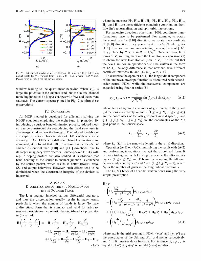
Fig. 9. (a) Current spectra of n-i-p TFET and (b) n-p-i-p TFET with 3-nmpocket length for VDS varying from −0.05 V to −0.25 V with −0.05 V step.Please refer to Fig. 8 for the device setting.
window leading to the quasi-linear behavior. When VDS islarge, the potential in the channel (and thus the source-channeltunneling junction) no longer changes with VDS and the currentsaturates. The current spectra plotted in Fig. 9 confirm theseobservations.
IV. CONCLUSION
An MOR method is developed for efficiently solving theNEGF equations employing the eight-band k · p model. Byintroducing a spurious band elimination process, reduced mod-els can be constructed for reproducing the band structures inany energy window near the bandgap. The reduced models canalso capture the I–V characteristics of TFETs with acceptableaccuracy. InAs TFETs with different channel orientations arecompared, it is found that [100] direction has better SS butsmaller ON-current than [110] and [111] directions, due toits larger imaginary wave vectors. Source-pocket TFETs withn-p-i-p doping profiles are also studied, it is observed thatband bending at the source-to-channel junction is enhancedby the source pocket, which results in better ON/OFF ratio,SS, and output behaviors. However, such effects tend to bediminished when the electrostatic integrity of the devices isimproved.
APPENDIX
DISCRETIZATION OF THE k · p HAMILTONIAN
IN THE FOURIER SPACE
The k · p operator involves various differential operators,and thus the discretization usually results in many terms,particularly when the number of bands is large. To havea discretized form that is compact and valid for arbitrarynanowire orientation, we rewrite the eight-band k · p operatorin (7) as [24]
H(
∂
∂x,
∂
∂y,
∂
∂z
)= −Hx x
∂2
∂x2 − Hyy∂2
∂y2 − Hzz∂2
∂z2
− Hxy∂2
∂x∂y− Hyz
∂2
∂y∂z− Hzx
∂2
∂z∂x
+ Hx∂
∂x+ Hy
∂
∂y+ Hz
∂
∂z+ H0 + Hso
(A-1)
where the matrices H0, Hso, Hx , Hy , Hz , Hx x , Hyy , Hzz , Hxy ,Hyz , and Hzx are the coefficients containing contributions fromLöwdin’s renormalization and spin-orbit interactions.
For nanowire directions other than [100], coordinate trans-formations have to be performed. For example, to obtainthe coordinate for [110] direction, we rotate the coordinateof [100] direction in xy plane by φ = π/4. Similarly, for[111] direction, we continue rotating the coordinate of [110]in yz plane by θ with sin θ = 1/
√3. Once we have k in
terms of k′, we plug them into the Hamiltonian expression (1)to obtain the new Hamiltonian (now in k′). It turns out thatthe new Hamiltonian operator can still be written in the formof (A-1), the only difference is that now we have differentcoefficient matrices Hi and Hi j (i, j = x, y, z).
To discretize the operator (A-1), the longitudinal componentof the unknown envelope function is discretized with second-order central FDM, while the transversal components areexpanded using Fourier series [8]
φp,q (ym, zn) = 2√Ny Nz
sin(k p ym
)sin
(kqzn
)(A-2)
where Ny and Nz are the number of grid points in the y andz directions respectively, m and n
(1 ≤ m ≤ Ny , 1 ≤ n ≤ Nz
)are the coordinates of the Rth grid point in real space, p andq
(1 ≤ p ≤ Ny , 1 ≤ q ≤ Nz
)are the coordinates of the Sth
grid point in the Fourier space
k p = pπ
L y, kq = qπ
Lz(A-3)
where L y (Lz) is the nanowire length in the y (z) direction.Operating (A-1) on (A-2), multiplying the result with (A-2)
and performing integrations, we get the discretized form. Itis block tridiagonal, with D being the on-site Hamiltonian forlayer l (1 ≤ l ≤ Nx ) and T being the coupling Hamiltonianbetween adjacent layers l and l + 1 (1 ≤ l ≤ Nx − 1), whereNx is the number of grids in the longitudinal direction x .
The(S, S′) block of D can be written down using the very
simple prescription
DS,S ′
=(
Hy4k ′
p
π
p
p2 − p′2
)δp+p′,oddδq,q ′
−(
Hyz4k ′
p
π
p
p2 − p′24k ′
q
π
q
q2 − q ′2
)δp+p′,oddδq+q ′,odd
+(
H0 + Hx x2
(�x)2 + Hyyk2p + Hzzk2
q + Hso
)δp,p′δq,q ′
+(
Hz4k ′
q
π
q
q2 − q ′2
)δq+q ′,oddδp,p′ (A-4)
where �x is the grid spacing in FDM, (p, q) and(
p′, q ′) arethe coordinates of the Sth and S′th grid points respectively,and δ is Kronecker delta function. For instance, δq+q ′,odd isequal to 1 (0) if q + q ′ is an odd (even) number.

568 IEEE TRANSACTIONS ON ELECTRON DEVICES, VOL. 61, NO. 2, FEBRUARY 2014
Similarly, the(S, S′) block of T can be written as
TS,S ′ =(
−Hx x1
(�x)2 + Hx1
2�x
)δp,p′δq,q ′
−(
Hxy1
2�x
4k ′p
π
p
p2 − p′2
)δp+p′,oddδq,q ′
−(
Hxz1
2�x
4k ′q
π
q
q2 − q ′2
)δq+q ′,oddδp,p′ . (A-5)
In this paper, we use �x = 0.125 nm and have limited Sto be 1 ≤ S ≤ 183 by employing the index scheme in [8].
ACKNOWLEDGMENT
The authors would like to thank J. Sun, Y. Zhang, S. Koofor setting up the computer cluster, and J. Peng, Q. Chen, andS. Markov for helpful discussions.
REFERENCES
[1] J. Deng and H.-S. Wong, “A compact SPICE model for carbon-nanotubefield-effect transistors including nonidealities and its application—Part I:Model of the intrinsic channel region,” IEEE Trans. Electron Devices,vol. 54, no. 12, pp. 3186–3194, Dec. 2007.
[2] D. A. Neamen, Semiconductor Physics and Devices: Basic Principles.New York, NY, USA: McGraw-Hill, 2003.
[3] J. Appenzeller, Y.-M. Lin, J. Knoch, Z. Chen, and P. Avouris, “Com-paring carbon nanotube transistors—The ideal choice: A novel tun-neling device design,” IEEE Trans. Electron Devices, vol. 52, no. 12,pp. 2568–2576, Dec. 2005.
[4] A. M. Ionescu and H. Riel, “Tunnel field-effect transistors as energy-efficient electronic switches,” Nature, vol. 479, no. 7373, pp. 329–337,Nov. 2011.
[5] (2013, Sep. 14). ITRS [Online]. Available: http://www.itrs.net/[6] S. Datta, Quantum Transport: Atom to Transistor. Cambridge, U.K.:
Cambridge Univ. Press, 2005.[7] M. Luisier and G. Klimeck, “Atomistic full-band design study of InAs
band-to-band tunneling field-effect transistors,” IEEE Electron DevicesLett., vol. 30, no. 6, pp. 602–604, Jun. 2009.
[8] M. Shin, “Full-quantum simulation of hole transport and band-to-bandtunneling in nanowires using the k · p method,” J. Appl. Phys., vol. 106,no. 5, pp. 054505-1–054505-10, Sep. 2009.
[9] G. Mil’nikov, N. Mori, and Y. Kamakura, “Equivalent transportmodels in atomistic quantum wires,” Phys. Rev. B, vol. 85, no. 3,pp. 035317-1–035317-11, 2012.
[10] J. Z. Huang, W. C. Chew, J. Peng, C.-Y. Yam, L. J. Jiang, andG.-H. Chen, “Model order reduction for multiband quantum transportsimulations and its application to p-type junctionless transistors,” IEEETrans. Electron Devices, vol. 60, no. 7, pp. 2111–2119, Jul. 2013.
[11] D. Gershoni, C. Henry, and G. Baraff, “Calculating the optical propertiesof multidimensional heterostructures: Application to the modeling ofquaternary quantum well lasers,” IEEE J. Quantum Electron., vol. 29,no. 9, pp. 2433–2450, Sep. 1993.
[12] P. Enders and M. Woerner, “Exact 4×4 block diagonalization of theeight-band k · p Hamiltonian matrix for tetrahedral semiconductors andits application to strained quantum wells,” Semicond. Sci. Technol.,vol. 11, no. 7, p. 983, 1996.
[13] R. G. Veprek, S. Steiger, and B. Witzigmann, “Ellipticity and thespurious solution problem of k · p envelope equations,” Phys. Rev. B,vol. 76, no. 16, pp. 165320-1–165320-9, 2007.
[14] M. Shin, S. Lee, and G. Klimeck, “Computational study on the perfor-mance of Si nanowire pMOSFETs based on the k · p method,” IEEETrans. Electron Devices, vol. 57, no. 9, pp. 2274–2283, Sep. 2010.
[15] A. Paussa, F. Conzatti, D. Breda, R. Vermiglio, D. Esseni, and P. Palestri,“Pseudospectral methods for the efficient simulation of quantizationeffects in nanoscale MOS transistors,” IEEE Trans. Electron Devices,vol. 57, no. 12, pp. 3239–3249, Dec. 2010.
[16] F. Conzatti, M. G. Pala, D. Esseni, E. Bano, and L. Selmi, “Strain-induced performance improvements in InAs nanowire tunnel FETs,”IEEE Trans. Electron Devices, vol. 59, no. 8, pp. 2085–2092, Aug. 2012.
[17] J. Guo, S. Datta, M. Lundstrom, and M. Anantam, “Toward multiscalemodeling of carbon nanotube transistors,” Int. J. Multiscale Comput.Eng., vol. 2, no. 2, pp. 257–276, 2004.
[18] A. C. Seabaugh and Q. Zhang, “Low-voltage tunnel transistors forbeyond CMOS logic,” Proc. IEEE, vol. 98, no. 12, pp. 2095–2110,Dec. 2010.
[19] R. Jhaveri, V. Nagavarapu, and J. C. Woo, “Effect of pocket doping andannealing schemes on the source-pocket tunnel field-effect transistor,”IEEE Trans. Electron Devices, vol. 58, no. 1, pp. 80–86, Jan. 2011.
[20] V. Nagavarapu, R. Jhaveri, and J. C. Woo, “The tunnel source (PNPN)n-MOSFET: A novel high performance transistor,” IEEE Trans. ElectronDevices, vol. 55, no. 4, pp. 1013–1019, Apr. 2008.
[21] Z. Chen, H. Yu, N. Singh, N. Shen, R. Sayanthan, G. Lo, et al.,“Demonstration of tunneling FETs based on highly scalable verti-cal silicon nanowires,” IEEE Electron Devices Lett., vol. 30, no. 7,pp. 754–756, Jul. 2009.
[22] H.-Y. Chang, B. Adams, P.-Y. Chien, J. Li, and J. C. Woo, “Improvedsubthreshold and output characteristics of source-pocket Si tunnel FETby the application of laser annealing,” IEEE Trans. Electron Devices,vol. 60, no. 1, pp. 92–96, Jan. 2013.
[23] D. Verreck, A. Verhulst, K.-H. Kao, W. Vandenberghe, K. De Meyer,and G. Groeseneken, “Quantum mechanical performance predictions ofp-n-i-n versus pocketed line tunnel field-effect transistors,” IEEE Trans.Electron Devices, vol. 60, no. 7, pp. 2128–2134, Jul. 2013.
[24] M. A. Khayer and R. K. Lake, “Modeling and performance analy-sis of GaN nanowire field-effect transistors and band-to-band tun-neling field-effect transistors,” J. Appl. Phys., vol. 108, no. 10,pp. 104503-1–104503-7, Nov. 2010.
Jun Z. Huang received the Ph.D. degree from The University of Hong Kong,Hong Kong, in November 2013. He joined Purdue University, West Lafayette,as a Post-Doctoral Researcher.
His current research interest is quantum transport simulation of nanoelec-tronic devices.
Lining Zhang (S’09–M’13) received the Ph.D. degree from the Hong KongUniversity of Science and Technology (HKUST), Hong Kong, in 2013.
He is currently a Research Associate with HKUST, and a Project Managerof i-MOS.
Weng Cho Chew (S’79–M’80–SM’86–F’93) received all his academicdegrees from the Massachusetts Institute of Technology, Cambridge, MA,USA.
His research interests are in wave and field physics.
Chi-Yung Yam received the B.Sc. and Ph.D. degrees in chemistry from theUniversity of Hong Kong, Hong Kong.
His current research interests include quantum transport and electronicdevice simulations.
Li Jun Jiang (S’01–M’04–SM’13) received the Ph.D. degree from theUniversity of Illinois at Urbana-Champaign, Urbana, IL, USA, in 2004.
His current research interests include electromagnetics, computationalelectromagnetics, IC signal/power integrity, antennas, and multidisciplinarycomputational solutions.
Guan-Hua Chen received the Ph.D. degree in physics from the CaliforniaInstitute of Technology, Pasadena, CA, USA, in 1992.
His current research interests include the development of first-principlesmethod for open systems and O(N) first-principles methods for excited states.
Mansun Chan (S’92–M’95–SM’01–F’13) received the Ph.D. degree fromthe University of California at Berkeley, Berkeley, CA, USA, in 1995.
He has been with the Faculty of Electrical and Computer Engineering,Hong Kong University of Science and Technology, Hong Kong, since 1996.