Embed Size (px)
Citation preview
MODEL OF STRESS INDUCED VOIDINGIN THE BACK-END-OF-LINE
OF A CMOS PROCESSF. Irrera, A. Nascetti
Dip. di Ingegneria Elettronica – Dip. Ingegneria Aerospaziale e AstronauticaUniversità degli Studi di Roma “La Sapienza”
F. Russo, M. SenaMicron Technology Italia, Avezzano
AbstractThis work provides a detailed and systematic analysis of the mechanisms inducing voiding during high temperature reliability tests in aluminum via-holes in a 130 nm process for CMOS imagers. Finite element simulations have been performed to derive the mechanical stress profile in the examined structures, while a set of physical measurements and microscopy techniques have been used to analyze the microstructure of the polycrystalline materials that fill the via-holes. Simulation results have been used to design a set of experiments, consisting in some simple changes in the fabrication technology steps, to compare the failure rate with reference samples of the production line. On the basis of both simulation and experimental results, a theoretical analysis of the mechanisms inducing voiding in aluminum via-holes in the Back-End-Of-Line (BEOL) of a real CMOS production process has been performed attempting a model of SIV.
Finite Elements Simulations
References[1] J.Curry, J. Fitzgibbon, G. Guan, Y. Muollo, R. Nelson, G. Thomas, “New failure mechanisms in sputtered aluminum silicon films”, IEEE Proceedings of the 22nd Int. Reliab. Physics Symp., Vol. 22, 6-8 (1984).[2] M. Gregoire, S. Kordic, M. Ignat, X. Federspiel, P. Vannier, S. Courtas, “New stress voiding observations in Cu interconnects”, Proceedings of the IEEE 2005 International, Interconnect Technology Conference, 36-38, (2005)[3] Z. Suo, Reliability of interconnect structures, 265-324 in volume 8: Interfacial and Nanoscale Failure (W.Gerberich, W.Yang Editors), Comprehensive Structural Integrity, Elsevir, Amsterdam, (2003)
Introduction
The failing via
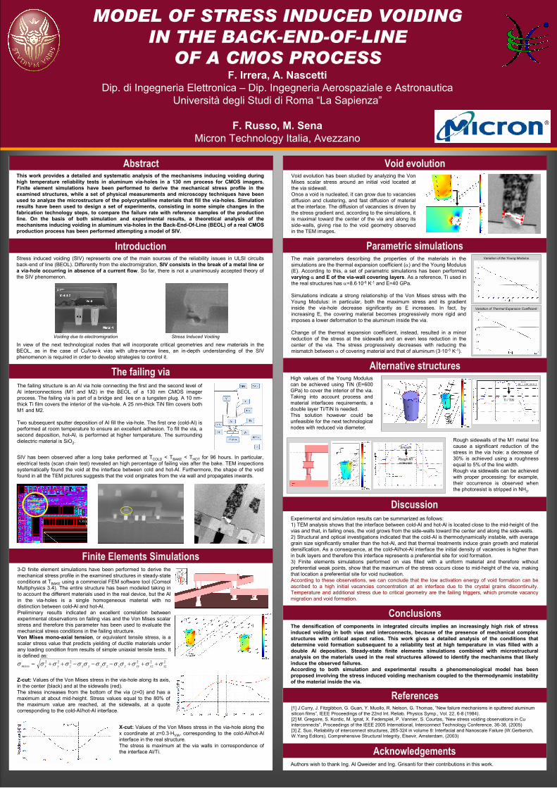
Void evolution
Discussion
ConclusionsThe densification of components in integrated circuits implies an increasingly high risk of stress induced voiding in both vias and interconnects, because of the presence of mechanical complex structures with critical aspect ratios. This work gives a detailed analysis of the conditions that determine void formation subsequent to a reliability test at high temperature in vias filled with a double Al deposition. Steady-state finite elements simulations combined with microstructuralanalysis on the materials used in the real structures allowed to identify the mechanisms that likely induce the observed failures.According to both simulation and experimental results a phenomenological model has been proposed involving the stress induced voiding mechanism coupled to the thermodynamic instability of the material inside the via.
Stress induced voiding (SIV) represents one of the main sources of the reliability issues in ULSI circuits back-end of line (BEOL). Differently from the electromigration, SIV consists in the break of a metal line or a via-hole occurring in absence of a current flow. So far, there is not a unanimously accepted theory of the SIV phenomenon.
In view of the next technological nodes that will incorporate critical geometries and new materials in the BEOL, as in the case of Cu/low-k vias with ultra-narrow lines, an in-depth understanding of the SIV phenomenon is required in order to develop strategies to control it.
The failing structure is an Al via hole connecting the first and the second level of Al interconnections (M1 and M2) in the BEOL of a 130 nm CMOS imager process. The failing via is part of a bridge and lies on a tungsten plug. A 10 nm-thick Ti film covers the interior of the via-hole. A 25 nm-thick TiN film covers both M1 and M2.
Two subsequent sputter deposition of Al fill the via-hole. The first one (cold-Al) is performed at room temperature to ensure an excellent adhesion. To fill the via, a second deposition, hot-Al, is performed at higher temperature. The surrounding dielectric material is SiO2.
AcknowledgementsAuthors wish to thank Ing. Al Qweider and Ing. Grisanti for their contributions in this work.
Voiding due to electromigration Stress Induced Voiding
Maximumfailuredensity
Experimental and simulation results can be summarized as follows:1) TEM analysis shows that the interface between cold-Al and hot-Al is located close to the mid-height of the vias and that, in failing ones, the void grows from the side-walls toward the center and along the side-walls.2) Structural and optical investigations indicated that the cold-Al is thermodynamically instable, with average grain size significantly smaller than the hot-Al, and that thermal treatments induce grain growth and materialdensification. As a consequence, at the cold-Al/hot-Al interface the initial density of vacancies is higher than in bulk layers and therefore this interface represents a preferential site for void formation.3) Finite elements simulations performed on vias filled with a uniform material and therefore without preferential weak points, show that the maximum of the stress occurs close to mid-height of the via, making that location a preferential site for void nucleation.According to these observations, we can conclude that the low activation energy of void formation can be ascribed to a high initial vacancies concentration at an interface due to the crystal grains discontinuity. Temperature and additional stress due to critical geometry are the failing triggers, which promote vacancy migration and void formation.
SIV has been observed after a long bake performed at TCOLD < TBAKE < THOT for 96 hours. In particular, electrical tests (scan chain test) revealed an high percentage of failing vias after the bake. TEM inspections systematically found the void at the interface between cold and hot-Al. Furthermore, the shape of the void found in all the TEM pictures suggests that the void originates from the via wall and propagates inwards.
222222xzyzxyzxzyyxzyxmises σσσσσσσσσσσσσ +++−−−++=
3-D finite element simulations have been performed to derive the mechanical stress profile in the examined structures in steady-state conditions at TBAKE using a commercial FEM software tool (ComsolMultiphysics 3.4). The entire structure has been modeled taking in to account the different materials used in the real device, but the Al in the via-holes is a single homogeneous material with no distinction between cold-Al and hot-Al.Preliminary results indicated an excellent correlation between experimental observations on failing vias and the Von Mises scalar stress and therefore this parameter has been used to evaluate the mechanical stress conditions in the failing structure. Von Mises mono-axial tension, or equivalent tensile stress, is a scalar stress value that predicts yielding of ductile materials under any loading condition from results of simple uniaxial tensile tests. It is defined as:
Parametric simulations
Alternative structures
Z-cut: Values of the Von Mises stress in the via-hole along its axis, in the center (black) and at the sidewalls (red). The stress increases from the bottom of the via (z=0) and has a maximum at about mid-height. Stress values equal to the 80% of the maximum value are reached, at the sidewalls, at a quote corresponding to the cold-Al/hot-Al interface.
X-cut: Values of the Von Mises stress in the via-hole along the x coordinate at z=0.3·HVIA, corresponding to the cold-Al/hot-Al interface in the real structure.The stress is maximum at the via walls in correspondence of the interface Al/Ti.
The main parameters describing the properties of the materials in the simulations are the thermal expansion coefficient (α) and the Young Modulus (E). According to this, a set of parametric simulations has been performed varying α and E of the via-wall covering layers. As a reference, Ti used in the real structures has α=8.6.10-6 K-1 and E=40 GPa.
Simulations indicate a strong relationship of the Von Mises stress with the Young Modulus: in particular, both the maximum stress and its gradient inside the via-hole decrease significantly as E increases. In fact, by increasing E, the covering material becomes progressively more rigid and imposes a lower deformation to the aluminum inside the via.
Change of the thermal expansion coefficient, instead, resulted in a minor reduction of the stress at the sidewalls and an even less reduction in the center of the via. The stress progressively decreases with reducing the mismatch between α of covering material and that of aluminum (3·10-5 K-1).
High values of the Young Modulus can be achieved using TiN (E=600 GPa) to cover the interior of the via. Taking into account process and material interfaces requirements, a double layer Ti/TiN is needed. This solution however could be unfeasible for the next technological nodes with reduced via diameter.
Ti
Ti / TiN
Rough sidewalls of the M1 metal line cause a significant reduction of the stress in the via hole: a decrease of 30% is achieved using a roughness equal to 5% of the line width.Rough via sidewalls can be achieved with proper processing: for example, their occurrence is observed when the photoresist is stripped in NH3.
Void evolution has been studied by analyzing the Von Mises scalar stress around an initial void located at the via sidewall.Once a void is nucleated, it can grow due to vacancies diffusion and clustering, and fast diffusion of material at the interface. The diffusion of vacancies is driven by the stress gradient and, according to the simulations, it is maximal toward the center of the via and along its side-walls, giving rise to the void geometry observed in the TEM images.
Variation of the Young Modulus
Variation of Thermal Expansion Coefficient
Smooth
Rough M1sidewalls