Embed Size (px)
Citation preview
Issued Date: Jun 13, 2007 Model No.: V315B1 - L07
Approval
Version 2.0
1
TFT LCD Approval Specification
MODEL NO.: V315B1 - L07
TVHD Approved By
LY Chen
QRA Dept. Product Development Div. Reviewed By
Tomy Chen WT Lin
LCD TV Marketing and Product Management Div. Prepared By
Denise Shieh Jim Ho
Customer:
Approved by:
Note:
Issued Date: Jun 13, 2007 Model No.: V315B1 - L07
Approval
Version 2.0
2
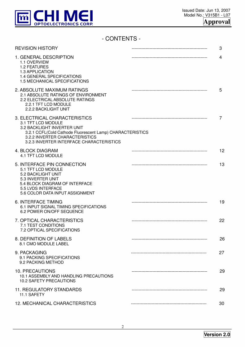
- CONTENTS - REVISION HISTORY ------------------------------------------------------- 3 1. GENERAL DESCRIPTION ------------------------------------------------------- 4
1.1 OVERVIEW 1.2 FEATURES 1.3 APPLICATION 1.4 GENERAL SPECIFICATIONS 1.5 MECHANICAL SPECIFICATIONS
2. ABSOLUTE MAXIMUM RATINGS ------------------------------------------------------- 5
2.1 ABSOLUTE RATINGS OF ENVIRONMENT 2.2 ELECTRICAL ABSOLUTE RATINGS
2.2.1 TFT LCD MODULE 2.2.2 BACKLIGHT UNIT 3. ELECTRICAL CHARACTERISTICS ------------------------------------------------------- 7
3.1 TFT LCD MODULE 3.2 BACKLIGHT INVERTER UNIT
3.2.1 CCFL(Cold Cathode Fluorescent Lamp) CHARACTERISTICS 3.2.2 INVERTER CHARACTERISTICS
3.2.3 INVERTER INTERFACE CHARACTERISTICS 4. BLOCK DIAGRAM ------------------------------------------------------- 12
4.1 TFT LCD MODULE 5. INTERFACE PIN CONNECTION ------------------------------------------------------- 13
5.1 TFT LCD MODULE 5.2 BACKLIGHT UNIT 5.3 INVERTER UNIT 5.4 BLOCK DIAGRAM OF INTERFACE 5.5 LVDS INTERFACE 5.6 COLOR DATA INPUT ASSIGNMENT
6. INTERFACE TIMING ------------------------------------------------------- 19
6.1 INPUT SIGNAL TIMING SPECIFICATIONS 6.2 POWER ON/OFF SEQUENCE
7. OPTICAL CHARACTERISTICS ------------------------------------------------------- 22
7.1 TEST CONDITIONS 7.2 OPTICAL SPECIFICATIONS
8. DEFINITION OF LABELS ------------------------------------------------------- 26
8.1 CMO MODULE LABEL
9. PACKAGING ------------------------------------------------------- 27 9.1 PACKING SPECIFICATIONS 9.2 PACKING METHOD
10. PRECAUTIONS ------------------------------------------------------- 29
10.1 ASSEMBLY AND HANDLING PRECAUTIONS 10.2 SAFETY PRECAUTIONS
11. REGULATORY STANDARDS ------------------------------------------------------- 29
11.1 SAFETY 12. MECHANICAL CHARACTERISTICS ------------------------------------------------------- 30
Issued Date: Jun 13, 2007 Model No.: V315B1 - L07
Approval
Version 2.0
3
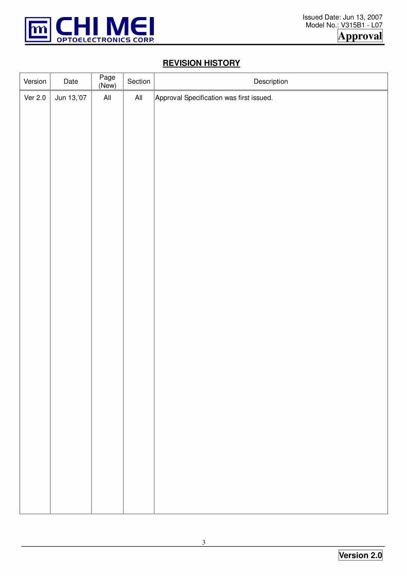
REVISION HISTORY
Version Date Page (New) Section Description
Ver 2.0
Jun 13,’07
All
All
Approval Specification was first issued.
Issued Date: Jun 13, 2007 Model No.: V315B1 - L07
Approval
Version 2.0
4
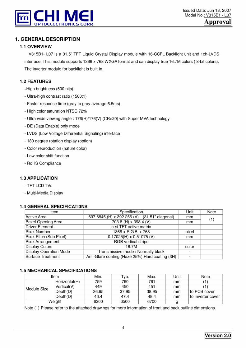
1. GENERAL DESCRIPTION 1.1 OVERVIEW
V315B1- L07 is a 31.5” TFT Liquid Crystal Display module with 16-CCFL Backlight unit and 1ch-LVDS
interface. This module supports 1366 x 768 WXGA format and can display true 16.7M colors ( 8-bit colors).
The inverter module for backlight is built-in.
1.2 FEATURES
- High brightness (500 nits)
- Ultra-high contrast ratio (1500:1)
- Faster response time (gray to gray average 6.5ms)
- High color saturation NTSC 72%
- Ultra wide viewing angle : 176(H)/176(V) (CR>20) with Super MVA technology
- DE (Data Enable) only mode
- LVDS (Low Voltage Differential Signaling) interface
- 180 degree rotation display (option)
- Color reproduction (nature color)
- Low color shift function
- RoHS Compliance
1.3 APPLICATION
- TFT LCD TVs
- Multi-Media Display
1.4 GENERAL SPECIFICATI0NS
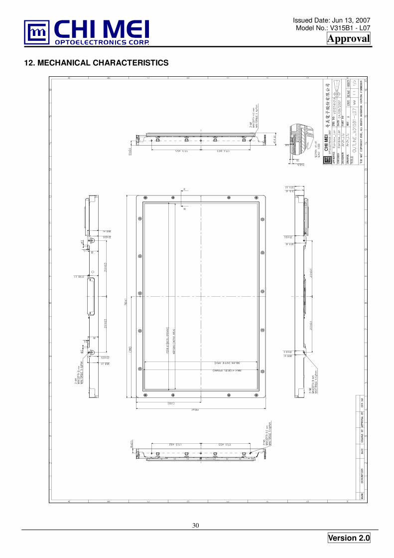
Item Specification Unit Note Active Area 697.6845 (H) x 392.256 (V) (31.51" diagonal) mm Bezel Opening Area 703.8 (H) x 398.4 (V) mm
(1)
Driver Element a-si TFT active matrix - Pixel Number 1366 x R.G.B. x 768 pixel Pixel Pitch (Sub Pixel) 0.17025(H) x 0.51075 (V) mm Pixel Arrangement RGB vertical stripe - Display Colors 16.7M color Display Operation Mode Transmissive mode / Normally black - Surface Treatment Anti-Glare coating (Haze 25%),Hard coating (3H) -
1.5 MECHANICAL SPECIFICATIONS Item Min. Typ. Max. Unit Note
Horizontal(H) 759 760 761 mm (1) Vertical(V) 449 450 451 mm (1) Depth(D) 36.95 37.95 38.95 mm To PCB cover
Module Size
Depth(D) 46.4 47.4 48.4 mm To inverter cover Weight 6300 6500 6700 g
Note (1) Please refer to the attached drawings for more information of front and back outline dimensions.
Issued Date: Jun 13, 2007 Model No.: V315B1 - L07
Approval
Version 2.0
5
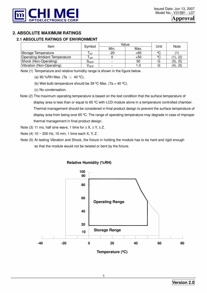
2. ABSOLUTE MAXIMUM RATINGS 2.1 ABSOLUTE RATINGS OF ENVIRONMENT
Value Item Symbol Min. Max.
Unit Note
Storage Temperature TST -20 +60 ºC (1) Operating Ambient Temperature TOP 0 +50 ºC (1), (2) Shock (Non-Operating) SNOP - 50 G (3), (5) Vibration (Non-Operating) VNOP - 1.0 G (4), (5)
Note (1) Temperature and relative humidity range is shown in the figure below.
(a) 90 %RH Max. (Ta � 40 ºC).
(b) Wet-bulb temperature should be 39 ºC Max. (Ta > 40 ºC).
(c) No condensation.
Note (2) The maximum operating temperature is based on the test condition that the surface temperature of
display area is less than or equal to 65 ºC with LCD module alone in a temperature controlled chamber.
Thermal management should be considered in final product design to prevent the surface temperature of
display area from being over 65 ºC. The range of operating temperature may degrade in case of improper
thermal management in final product design.
Note (3) 11 ms, half sine wave, 1 time for ± X, ± Y, ± Z.
Note (4) 10 ~ 200 Hz, 10 min, 1 time each X, Y, Z.
Note (5) At testing Vibration and Shock, the fixture in holding the module has to be hard and rigid enough
so that the module would not be twisted or bent by the fixture.
Relative Humidity (%RH)
Operating Range
Temperature (ºC)
100
80 60 -20 40 0 20 -40
90
80
40
60
20
10 Storage Range
Issued Date: Jun 13, 2007 Model No.: V315B1 - L07
Approval
Version 2.0
6
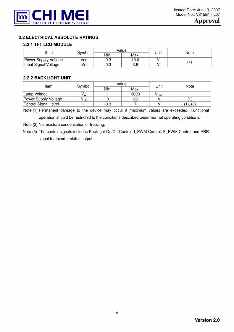
2.2 ELECTRICAL ABSOLUTE RATINGS
2.2.1 TFT LCD MODULE Value Item Symbol
Min. Max. Unit Note
Power Supply Voltage Vcc -0.3 13.0 V Input Signal Voltage VIN -0.3 3.6 V
(1)
2.2.2 BACKLIGHT UNIT Value Item Symbol
Min. Max. Unit Note
Lamp Voltage VW � 3000 VRMS Power Supply Voltage VBL 0 30 V (1) Control Signal Level � -0.3 7 V (1), (3)
Note (1) Permanent damage to the device may occur if maximum values are exceeded. Functional
operation should be restricted to the conditions described under normal operating conditions.
Note (2) No moisture condensation or freezing.
Note (3) The control signals includes Backlight On/Off Control, I_PWM Control, E_PWM Control and ERR
signal for inverter status output.
Issued Date: Jun 13, 2007 Model No.: V315B1 - L07
Approval
Version 2.0
7
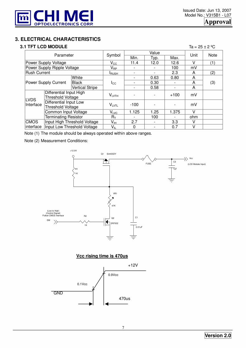
3. ELECTRICAL CHARACTERISTICS 3.1 TFT LCD MODULE Ta = 25 ± 2 ºC
Value Parameter Symbol Min. Typ. Max.
Unit Note
Power Supply Voltage VCC 11.4 12.0 12.6 V (1) Power Supply Ripple Voltage VRP - - 100 mV Rush Current IRUSH - - 2.3 A (2)
White - 0.63 0.80 A Black - 0.30 - A Power Supply Current Vertical Stripe
ICC - 0.58 - A
(3)
Differential Input High Threshold Voltage VLVTH - - +100 mV
Differential Input Low Threshold Voltage VLVTL -100 - - mV
Common Input Voltage VLVC 1.125 1.25 1.375 V
LVDS Interface
Terminating Resistor RT - 100 - ohm Input High Threshold Voltage VIH 2.7 - 3.3 V CMOS
interface Input Low Threshold Voltage VIL 0 - 0.7 V
Note (1) The module should be always operated within above ranges.
Note (2) Measurement Conditions:
Vcc rising time is 470us
470us
+12V
GND
0.9Vcc
0.1Vcc
VR1
47K
Q2 2N7002
(Low to High) (Control Signal)
Follow CMOS interface SW
R2
1K
C1
0.01uF
Vcc C3 1uF
(LCD Module Input) FUSE R1
+12.0V Q1 Si4435DY
1K
Issued Date: Jun 13, 2007 Model No.: V315B1 - L07
Approval
Version 2.0
8
Note (3) The specified power supply current is under the conditions at Vcc = 12 V, Ta = 25 ± 2 ºC, fv = 60
Hz, whereas a power dissipation check pattern below is displayed.
3.2 BACKLIGHT INVERTER UNIT
3.2.1 CCFL (Cold Cathode Fluorescent Lamp) CHARACTERISTICS (Ta = 25 ± 2 ºC) Value
Parameter Symbol Min. Typ. Max.
Unit Note
Lamp Voltage VW - 1250 - VRMS IL = 5.2mA Lamp Current IL 4.7 5.2 5.7 mARMS (1)
- - 2450 VRMS (2), Ta = 0 ºC Lamp Starting Voltage VS - - 2360 VRMS (2), Ta = 25 ºC Operating Frequency FO 40 - 70 KHz (3) Lamp Life Time LBL 50,000 - Hrs (4)
Active Area
c. Vertical Stripe Pattern
R
R
R
R
R R
R
R
G
G
G
G
B
B
B
B
B
B
G
G
G
G
B
B
B
B
R
R
Active Area Active Area
a. White Pattern b. Black Pattern
Issued Date: Jun 13, 2007 Model No.: V315B1 - L07
Approval
Version 2.0
9
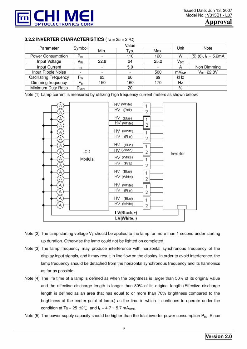
3.2.2 INVERTER CHARACTERISTICS (Ta = 25 ± 2 ºC) Value
Parameter Symbol Min. Typ. Max.
Unit Note
Power Consumption PBL - 110 120 W (5),(6), IL = 5.2mA Input Voltage VBL 22.8 24 25.2 VDC Input Current IBL - 5.0 - A Non Dimming
Input Ripple Noise - - - 500 mVP-P VBL=22.8V Oscillating Frequency FW 63 66 69 kHz Dimming frequency FB 150 160 170 Hz Minimum Duty Ratio DMIN - 20 - %
Note (1) Lamp current is measured by utilizing high frequency current meters as shown below:
Note (2) The lamp starting voltage VS should be applied to the lamp for more than 1 second under starting
up duration. Otherwise the lamp could not be lighted on completed.
Note (3) The lamp frequency may produce interference with horizontal synchronous frequency of the
display input signals, and it may result in line flow on the display. In order to avoid interference, the
lamp frequency should be detached from the horizontal synchronous frequency and its harmonics
as far as possible.
Note (4) The life time of a lamp is defined as when the brightness is larger than 50% of its original value
and the effective discharge length is longer than 80% of its original length (Effective discharge
length is defined as an area that has equal to or more than 70% brightness compared to the
brightness at the center point of lamp.) as the time in which it continues to operate under the
condition at Ta = 25 �2� and IL = 4.7 ~ 5.7 mARMS.
Note (5) The power supply capacity should be higher than the total inverter power consumption PBL. Since
Issued Date: Jun 13, 2007 Model No.: V315B1 - L07
Approval
Version 2.0
10
the pulse width modulation (PWM) mode was applied for backlight dimming, the driving current
changed as PWM duty on and off. The transient response of power supply should be considered
for the changing loading when inverter dimming.
Note (6) The measurement condition of Max. value is based on 31.5" backlight unit under input voltage 24V,
average lamp current 5.5 mA and lighting 30 minutes later.
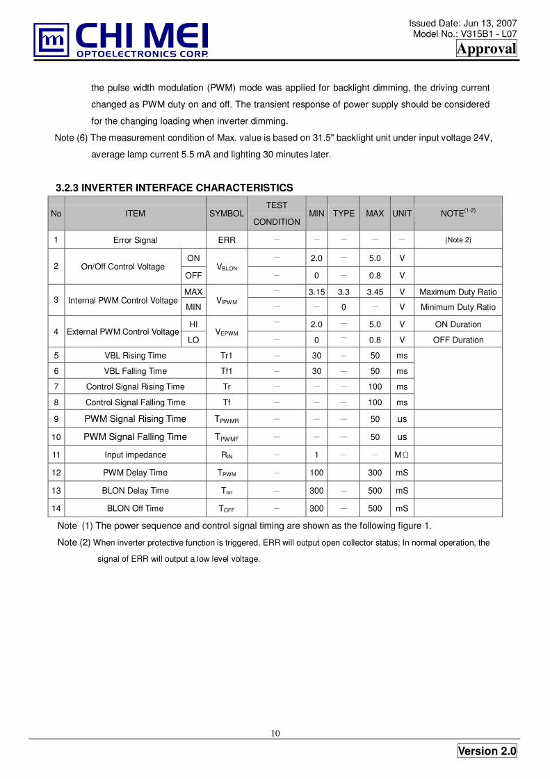
3.2.3 INVERTER INTERFACE CHARACTERISTICS
No ITEM SYMBOL TEST
CONDITION MIN TYPE MAX UNIT NOTE(1-2)
1 Error Signal ERR � � � � � (Note 2)
ON � 2.0 � 5.0 V 2 On/Off Control Voltage
OFF VBLON
� 0 � 0.8 V
MAX � 3.15 3.3 3.45 V Maximum Duty Ratio 3 Internal PWM Control Voltage
MIN VIPWM
� � 0 � V Minimum Duty Ratio
HI � 2.0 � 5.0 V ON Duration 4 External PWM Control Voltage
LO VEPWM
� 0 � 0.8 V OFF Duration
5 VBL Rising Time Tr1 � 30 � 50 ms
6 VBL Falling Time Tf1 � 30 � 50 ms
7 Control Signal Rising Time Tr � � � 100 ms
8 Control Signal Falling Time Tf � � � 100 ms
9 PWM Signal Rising Time TPWMR � � � 50 us
10 PWM Signal Falling Time TPWMF � � � 50 us
11 Input impedance RIN � 1 � � M�
12 PWM Delay Time TPWM � 100 300 mS
13 BLON Delay Time Ton � 300 � 500 mS
14 BLON Off Time TOFF � 300 � 500 mS
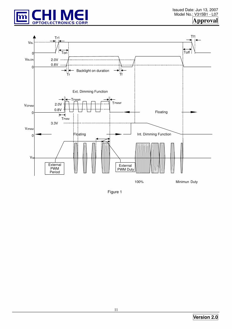
Note (1) The power sequence and control signal timing are shown as the following figure 1.
Note (2) When inverter protective function is triggered, ERR will output open collector status; In normal operation, the
signal of ERR will output a low level voltage.
Issued Date: Jun 13, 2007 Model No.: V315B1 - L07
Approval
Version 2.0
11
2.0V0.8V
Tr TfBacklight on duration
0
VEPWM
3.3VVIPWM
VW
Int. Dimming Function
Ton
Minimun Duty100%
ExternalPWM Duty
VBL
VBLON
0
0
0
2.0V
0.8V
Toff
ExternalPWMPeriod
Tr1 Tf1
Ext. Dimming Function
TPWMFTPWMR
TPWM
Floating
Floating
Figure 1
Issued Date: Jun 13, 2007 Model No.: V315B1 - L07
Approval
Version 2.0
12
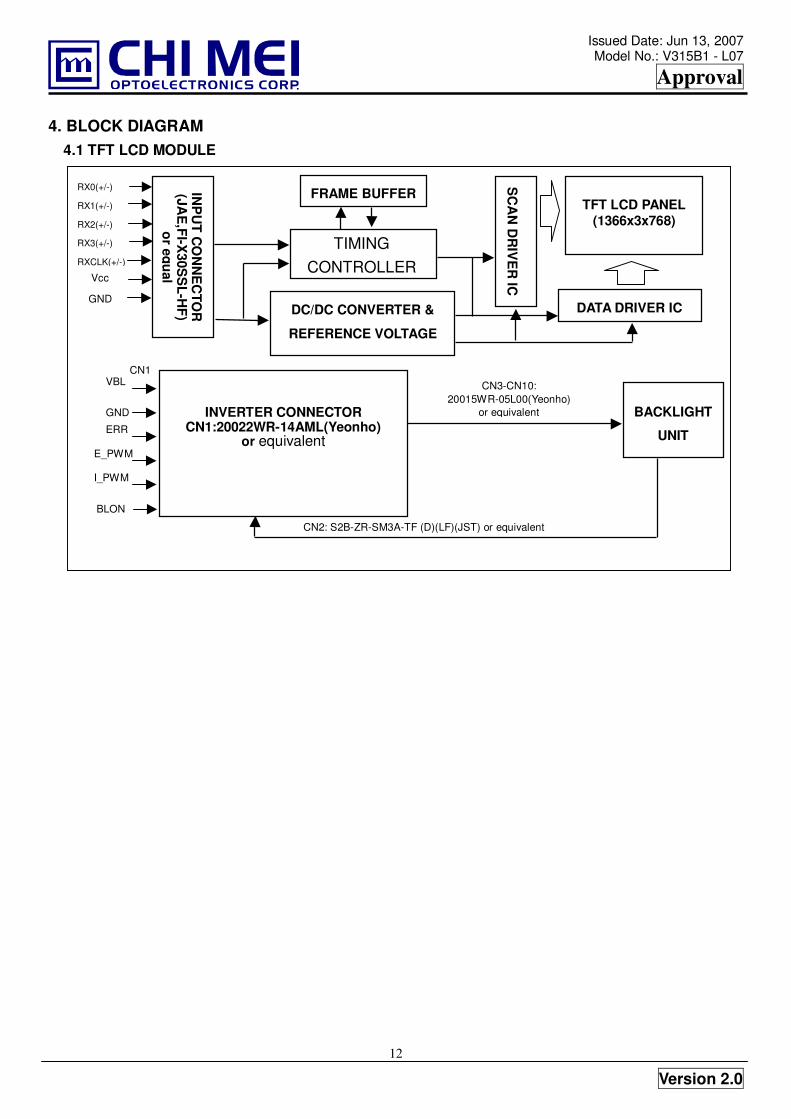
4. BLOCK DIAGRAM 4.1 TFT LCD MODULE
TFT LCD PANEL
(1366x3x768)
DATA DRIVER IC
SC
AN
DR
IVE
R IC
DC/DC CONVERTER &
REFERENCE VOLTAGE
INP
UT C
ON
NE
CTO
R
(JAE
,FI-X30S
SL-H
F) or equal
GND
Vcc
FRAME BUFFER
RX0(+/-)
RX1(+/-)
RX2(+/-)
RX3(+/-)
RXCLK(+/-) TIMING CONTROLLER
BACKLIGHT
UNIT
INVERTER CONNECTOR CN1:20022WR-14AML(Yeonho)
or equivalent
CN3-CN10: 20015WR-05L00(Yeonho)
or equivalent
CN1
CN2: S2B-ZR-SM3A-TF (D)(LF)(JST) or equivalent
GND
E_PWM
I_PWM
BLON
VBL
ERR
Issued Date: Jun 13, 2007 Model No.: V315B1 - L07
Approval
Version 2.0
13
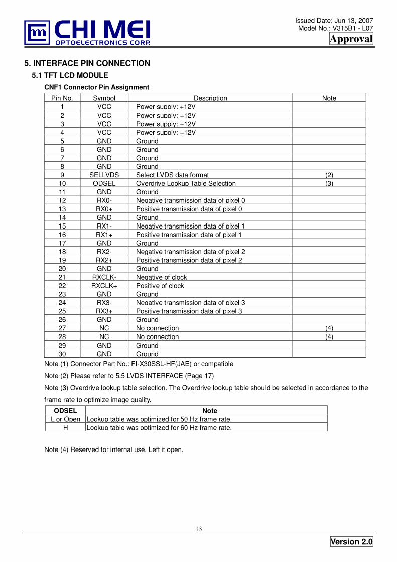
5. INTERFACE PIN CONNECTION 5.1 TFT LCD MODULE
CNF1 Connector Pin Assignment
Pin No. Symbol Description Note 1 VCC Power supply: +12V 2 VCC Power supply: +12V 3 VCC Power supply: +12V 4 VCC Power supply: +12V 5 GND Ground 6 GND Ground 7 GND Ground 8 GND Ground 9 SELLVDS Select LVDS data format (2)
10 ODSEL Overdrive Lookup Table Selection (3) 11 GND Ground 12 RX0- Negative transmission data of pixel 0 13 RX0+ Positive transmission data of pixel 0 14 GND Ground 15 RX1- Negative transmission data of pixel 1 16 RX1+ Positive transmission data of pixel 1 17 GND Ground 18 RX2- Negative transmission data of pixel 2 19 RX2+ Positive transmission data of pixel 2 20 GND Ground 21 RXCLK- Negative of clock 22 RXCLK+ Positive of clock 23 GND Ground 24 RX3- Negative transmission data of pixel 3 25 RX3+ Positive transmission data of pixel 3 26 GND Ground 27 NC No connection (4) 28 NC No connection (4) 29 GND Ground 30 GND Ground
Note (1) Connector Part No.: FI-X30SSL-HF(JAE) or compatible
Note (2) Please refer to 5.5 LVDS INTERFACE (Page 17)
Note (3) Overdrive lookup table selection. The Overdrive lookup table should be selected in accordance to the
frame rate to optimize image quality.
ODSEL Note L or Open Lookup table was optimized for 50 Hz frame rate.
H Lookup table was optimized for 60 Hz frame rate.
Note (4) Reserved for internal use. Left it open.
Issued Date: Jun 13, 2007 Model No.: V315B1 - L07
Approval
Version 2.0
14
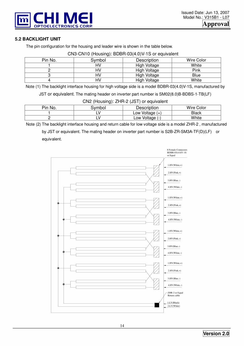
5.2 BACKLIGHT UNIT
The pin configuration for the housing and leader wire is shown in the table below.
CN3-CN10 (Housing): BDBR-03(4.0)V-1S or equivalent Pin No. Symbol Description Wire Color
1 HV High Voltage White 2 HV High Voltage Pink 3 HV High Voltage Blue 4 HV High Voltage White
Note (1) The backlight interface housing for high voltage side is a model BDBR-03(4.0)V-1S, manufactured by
JST or equivalent. The mating header on inverter part number is SM02(8.0)B-BDBS-1-TB(LF)
CN2 (Housing): ZHR-2 (JST) or equivalent Pin No. Symbol Description Wire Color
1 LV Low Voltage (+) Black 2 LV Low Voltage (-) White
Note (2) The backlight interface housing and return cable for low voltage side is a model ZHR-2 , manufactured
by JST or equivalent. The mating header on inverter part number is S2B-ZR-SM3A-TF(D)(LF) or
equivalent.
8 Female ConnectorsBDBR-03(4.0)V-1Sor Equal
ZHR-2 or EqualReturn cable
1.LV(Black)2.LV(White)
1.HV(White,+)
4.HV(White,-)
2.HV(Pink,+)
3.HV(Blue,-)
4.HV(White,-)
1.HV(White,+)
3.HV(Blue,-)
2.HV(Pink,+)
4.HV(White,-)
1.HV(White,+)
3.HV(Blue,-)
2.HV(Pink,�)
4.HV(White,-)
1.HV(White,+)
3.HV(Blue,-)
2.HV(Pink,+)
Issued Date: Jun 13, 2007 Model No.: V315B1 - L07
Approval
Version 2.0
15
5.3 INVERTER UNIT
CN1(Header): 20022WR-14AML(Yeonho) or equivalent.. Pin No. Symbol Description
1 2 3 4 5
VBL +24V Power input
6 7 8 9
10
GND Ground
11 ERR Normal (GND) Abnormal ( open collector)
12 BLON Backlight on/off control 13 I_PWM Internal PWM control signal 14 E_PWM External PWM control signal
Notice:
#PIN 13:Analog Dimming Control (Use Pin 13) : 0V~3.3V and Pin 14 must open.
#PIN 14:PWM Dimming Control (Use Pin 14) : Pin 13 must open.
#Pin 13(I_PWM) and Pin 14(E_PWM) can not open in same period.
CN2(Header): S2B-ZR-SM3A-TF(D)(LF)(JST) or equivalent Pin No. Symbol Description
1 CCFL COLD CCFL low voltage (+) 2 CCFL COLD CCFL low voltage (-)
CN3-CN10 (Header): 20015WR-05L00(Yeonho) or equivalent. Pin No. Symbol Description
1 CCFL HOT CCFL high voltage 2 CCFL HOT CCFL high voltage
Issued Date: Jun 13, 2007 Model No.: V315B1 - L07
Approval
Version 2.0
16
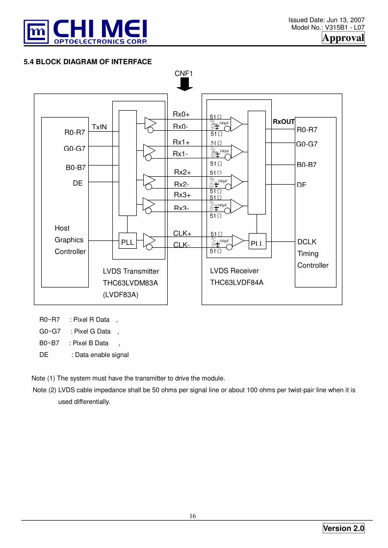
5.4 BLOCK DIAGRAM OF INTERFACE
CNF1
R0~R7 : Pixel R Data ,
G0~G7 : Pixel G Data ,
B0~B7 : Pixel B Data ,
DE : Data enable signal
Note (1) The system must have the transmitter to drive the module.
Note (2) LVDS cable impedance shall be 50 ohms per signal line or about 100 ohms per twist-pair line when it is
used differentially.
R0-R7
G0-G7
B0-B7
DE
Host
Graphics
Controller
TxIN
PLL PLL
R0-R7
G0-G7
B0-B7
DE
DCLK
Timing
Controller LVDS Transmitter
THC63LVDM83A
(LVDF83A)
LVDS Receiver
THC63LVDF84A
Rx0+
Rx0-
Rx1+ Rx1-
Rx2+
Rx2-
CLK+
CLK-
RxOUT 51�
51�
51�
51�
51�
51� 51�
51�
51�
51�
100pF
100pF
100pF
100pF
100pF
Rx3-
Rx3+
Issued Date: Jun 13, 2007 Model No.: V315B1 - L07
Approval
Version 2.0
17
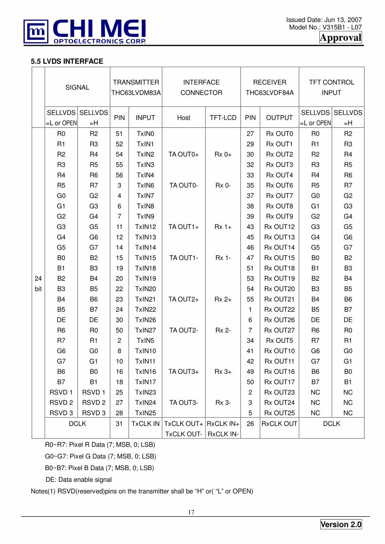
5.5 LVDS INTERFACE
SIGNAL TRANSMITTER
THC63LVDM83A
INTERFACE
CONNECTOR
RECEIVER
THC63LVDF84A
TFT CONTROL
INPUT
SELLVDS
=L or OPEN
SELLVDS
=H PIN INPUT Host TFT-LCD PIN OUTPUT
SELLVDS
=L or OPEN
SELLVDS
=H
R0
R1
R2
R3
R4
R5
G0
G1
G2
G3
G4
G5
B0
B1
B2
B3
B4
B5
DE
R6
R7
G6
G7
B6
B7
RSVD 1
RSVD 2
RSVD 3
R2
R3
R4
R5
R6
R7
G2
G3
G4
G5
G6
G7
B2
B3
B4
B5
B6
B7
DE
R0
R1
G0
G1
B0
B1
RSVD 1
RSVD 2
RSVD 3
51
52
54
55
56
3
4
6
7
11
12
14
15
19
20
22
23
24
30
50
2
8
10
16
18
25
27
28
TxIN0
TxIN1
TxIN2
TxIN3
TxIN4
TxIN6
TxIN7
TxIN8
TxIN9
TxIN12
TxIN13
TxIN14
TxIN15
TxIN18
TxIN19
TxIN20
TxIN21
TxIN22
TxIN26
TxIN27
TxIN5
TxIN10
TxIN11
TxIN16
TxIN17
TxIN23
TxIN24
TxIN25
TA OUT0+
TA OUT0-
TA OUT1+
TA OUT1-
TA OUT2+
TA OUT2-
TA OUT3+
TA OUT3-
Rx 0+
Rx 0-
Rx 1+
Rx 1-
Rx 2+
Rx 2-
Rx 3+
Rx 3-
27
29
30
32
33
35
37
38
39
43
45
46
47
51
53
54
55
1
6
7
34
41
42
49
50
2
3
5
Rx OUT0
Rx OUT1
Rx OUT2
Rx OUT3
Rx OUT4
Rx OUT6
Rx OUT7
Rx OUT8
Rx OUT9
Rx OUT12
Rx OUT13
Rx OUT14
Rx OUT15
Rx OUT18
Rx OUT19
Rx OUT20
Rx OUT21
Rx OUT22
Rx OUT26
Rx OUT27
Rx OUT5
Rx OUT10
Rx OUT11
Rx OUT16
Rx OUT17
Rx OUT23
Rx OUT24
Rx OUT25
R0
R1
R2
R3
R4
R5
G0
G1
G2
G3
G4
G5
B0
B1
B2
B3
B4
B5
DE
R6
R7
G6
G7
B6
B7
NC
NC
NC
R2
R3
R4
R5
R6
R7
G2
G3
G4
G5
G6
G7
B2
B3
B4
B5
B6
B7
DE
R0
R1
G0
G1
B0
B1
NC
NC
NC
24
bit
DCLK 31 TxCLK IN TxCLK OUT+
TxCLK OUT-
RxCLK IN+
RxCLK IN-
26 RxCLK OUT DCLK
R0~R7: Pixel R Data (7; MSB, 0; LSB)
G0~G7: Pixel G Data (7; MSB, 0; LSB)
B0~B7: Pixel B Data (7; MSB, 0; LSB)
DE: Data enable signal
Notes(1) RSVD(reserved)pins on the transmitter shall be “H” or( “L” or OPEN)
Issued Date: Jun 13, 2007 Model No.: V315B1 - L07
Approval
Version 2.0
18
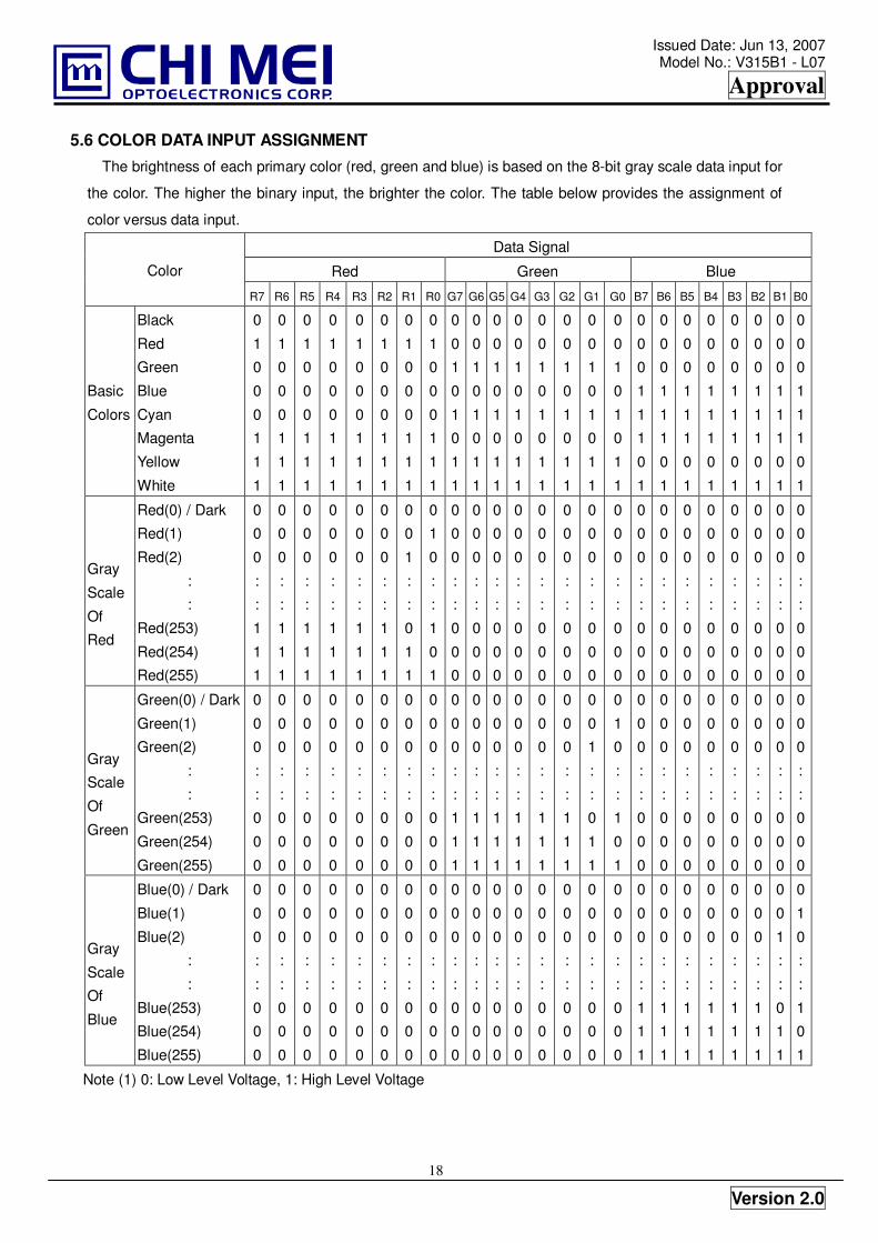
5.6 COLOR DATA INPUT ASSIGNMENT
The brightness of each primary color (red, green and blue) is based on the 8-bit gray scale data input for
the color. The higher the binary input, the brighter the color. The table below provides the assignment of
color versus data input.
Data Signal
Red Green Blue Color
R7 R6 R5 R4 R3 R2 R1 R0 G7 G6 G5 G4 G3 G2 G1 G0 B7 B6 B5 B4 B3 B2 B1 B0
Basic
Colors
Black
Red
Green
Blue
Cyan
Magenta
Yellow
White
0
1
0
0
0
1
1
1
0
1
0
0
0
1
1
1
0
1
0
0
0
1
1
1
0
1
0
0
0
1
1
1
0
1
0
0
0
1
1
1
0
1
0
0
0
1
1
1
0
1
0
0
0
1
1
1
0
1
0
0
0
1
1
1
0
0
1
0
1
0
1
1
0
0
1
0
1
0
1
1
0
0
1
0
1
0
1
1
0
0
1
0
1
0
1
1
0
0
1
0
1
0
1
1
0
0
1
0
1
0
1
1
0
0
1
0
1
0
1
1
0
0
1
0
1
0
1
1
0
0
0
1
1
1
0
1
0
0
0
1
1
1
0
1
0
0
0
1
1
1
0
1
0
0
0
1
1
1
0
1
0
0
0
1
1
1
0
1
0
0
0
1
1
1
0
1
0
0
0
1
1
1
0
1
0
0
0
1
1
1
0
1
Gray
Scale
Of
Red
Red(0) / Dark
Red(1)
Red(2)
:
:
Red(253)
Red(254)
Red(255)
0
0
0
:
:
1
1
1
0
0
0
:
:
1
1
1
0
0
0
:
:
1
1
1
0
0
0
:
:
1
1
1
0
0
0
:
:
1
1
1
0
0
0
:
:
1
1
1
0
0
1
:
:
0
1
1
0
1
0
:
:
1
0
1
0
0
0
:
:
0
0
0
0
0
0
:
:
0
0
0
0
0
0
:
:
0
0
0
0
0
0
:
:
0
0
0
0
0
0
:
:
0
0
0
0
0
0
:
:
0
0
0
0
0
0
:
:
0
0
0
0
0
0
:
:
0
0
0
0
0
0
:
:
0
0
0
0
0
0
:
:
0
0
0
0
0
0
:
:
0
0
0
0
0
0
:
:
0
0
0
0
0
0
:
:
0
0
0
0
0
0
:
:
0
0
0
0
0
0
:
:
0
0
0
0
0
0
:
:
0
0
0
Gray
Scale
Of
Green
Green(0) / Dark
Green(1)
Green(2)
:
:
Green(253)
Green(254)
Green(255)
0
0
0
:
:
0
0
0
0
0
0
:
:
0
0
0
0
0
0
:
:
0
0
0
0
0
0
:
:
0
0
0
0
0
0
:
:
0
0
0
0
0
0
:
:
0
0
0
0
0
0
:
:
0
0
0
0
0
0
:
:
0
0
0
0
0
0
:
:
1
1
1
0
0
0
:
:
1
1
1
0
0
0
:
:
1
1
1
0
0
0
:
:
1
1
1
0
0
0
:
:
1
1
1
0
0
0
:
:
1
1
1
0
0
1
:
:
0
1
1
0
1
0
:
:
1
0
1
0
0
0
:
:
0
0
0
0
0
0
:
:
0
0
0
0
0
0
:
:
0
0
0
0
0
0
:
:
0
0
0
0
0
0
:
:
0
0
0
0
0
0
:
:
0
0
0
0
0
0
:
:
0
0
0
0
0
0
:
:
0
0
0
Gray
Scale
Of
Blue
Blue(0) / Dark
Blue(1)
Blue(2)
:
:
Blue(253)
Blue(254)
Blue(255)
0
0
0
:
:
0
0
0
0
0
0
:
:
0
0
0
0
0
0
:
:
0
0
0
0
0
0
:
:
0
0
0
0
0
0
:
:
0
0
0
0
0
0
:
:
0
0
0
0
0
0
:
:
0
0
0
0
0
0
:
:
0
0
0
0
0
0
:
:
0
0
0
0
0
0
:
:
0
0
0
0
0
0
:
:
0
0
0
0
0
0
:
:
0
0
0
0
0
0
:
:
0
0
0
0
0
0
:
:
0
0
0
0
0
0
:
:
0
0
0
0
0
0
:
:
0
0
0
0
0
0
:
:
1
1
1
0
0
0
:
:
1
1
1
0
0
0
:
:
1
1
1
0
0
0
:
:
1
1
1
0
0
0
:
:
1
1
1
0
0
0
:
:
1
1
1
0
0
1
:
:
0
1
1
0
1
0
:
:
1
0
1
Note (1) 0: Low Level Voltage, 1: High Level Voltage
Issued Date: Jun 13, 2007 Model No.: V315B1 - L07
Approval
Version 2.0
19
Tvd Tvb
Tv
Th
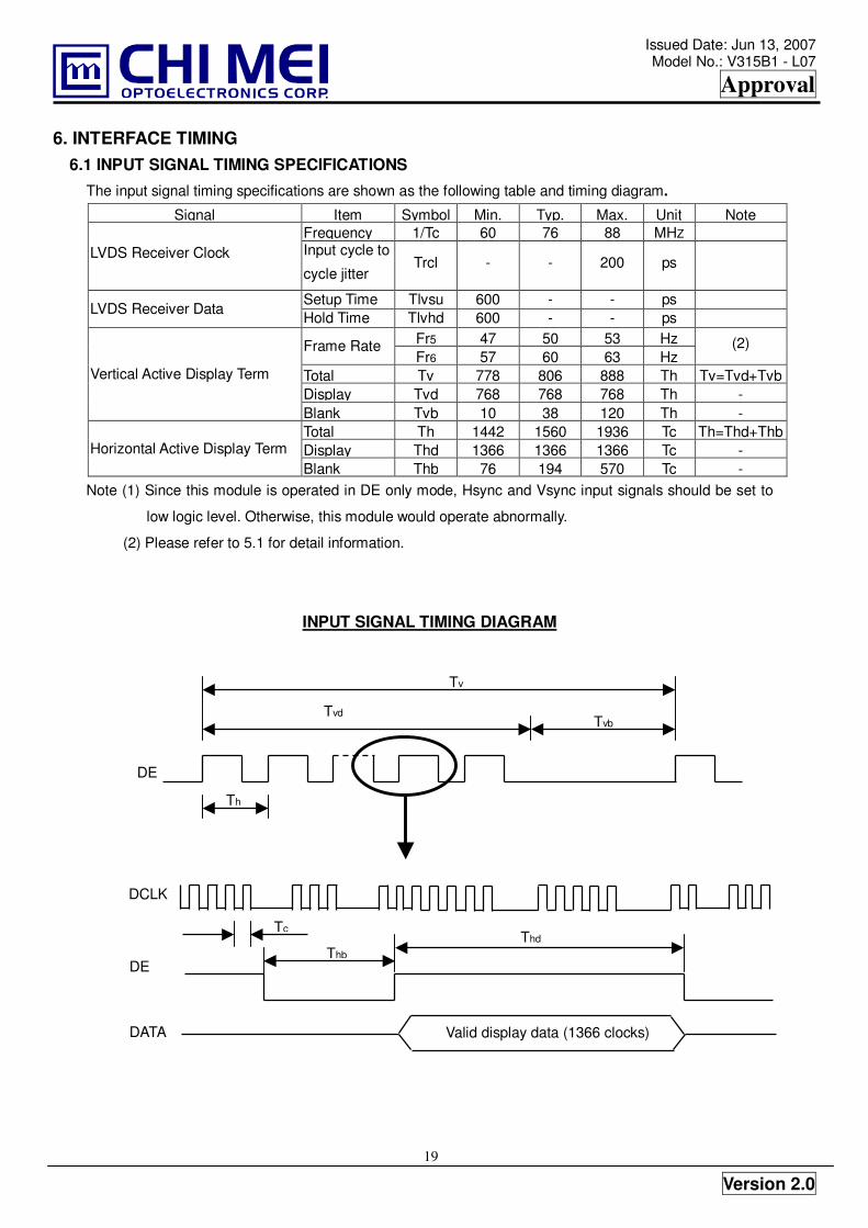
6. INTERFACE TIMING 6.1 INPUT SIGNAL TIMING SPECIFICATIONS
The input signal timing specifications are shown as the following table and timing diagram.
Signal Item Symbol Min. Typ. Max. Unit Note Frequency 1/Tc 60 76 88 MHZ
LVDS Receiver Clock Input cycle to
cycle jitter Trcl - - 200 ps
Setup Time Tlvsu 600 - - ps LVDS Receiver Data Hold Time Tlvhd 600 - - ps
Fr5 47 50 53 Hz Frame Rate Fr6 57 60 63 Hz
(2)
Total Tv 778 806 888 Th Tv=Tvd+Tvb Display Tvd 768 768 768 Th -
Vertical Active Display Term
Blank Tvb 10 38 120 Th - Total Th 1442 1560 1936 Tc Th=Thd+Thb Display Thd 1366 1366 1366 Tc - Horizontal Active Display Term Blank Thb 76 194 570 Tc -
Note (1) Since this module is operated in DE only mode, Hsync and Vsync input signals should be set to
low logic level. Otherwise, this module would operate abnormally.
(2) Please refer to 5.1 for detail information.
INPUT SIGNAL TIMING DIAGRAM
DE
Thb
Valid display data (1366 clocks)
Tc
DCLK
Thd
DE
DATA
Issued Date: Jun 13, 2007 Model No.: V315B1 - L07
Approval
Version 2.0
20
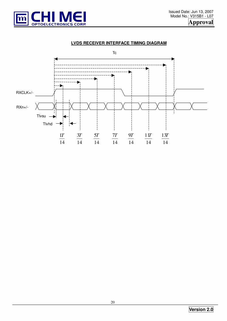
LVDS RECEIVER INTERFACE TIMING DIAGRAM
RXCLK+/-
RXn+/-
141T
143T
145T
147T
149T
1411T
1413T
Tlvsu
Tlvhd
Tc
Issued Date: Jun 13, 2007 Model No.: V315B1 - L07
Approval
Version 2.0
21
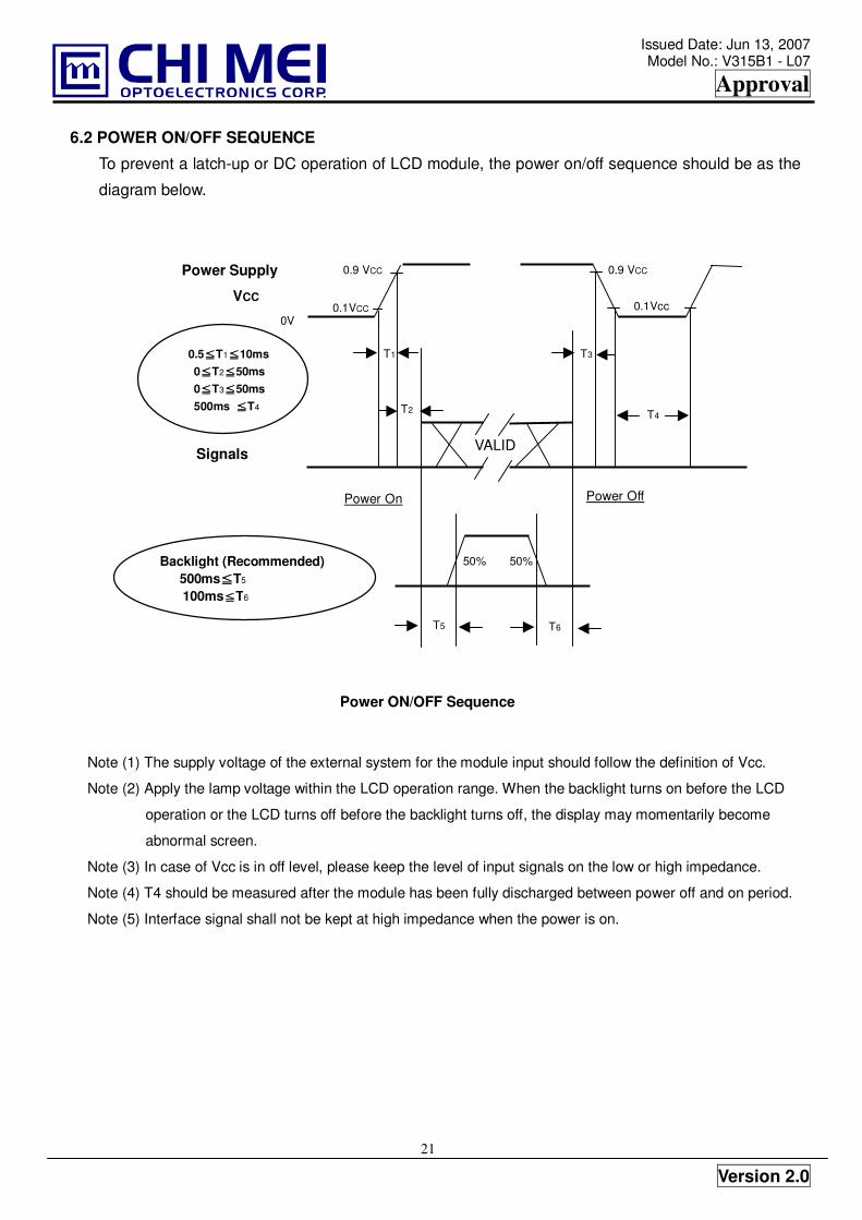
0.5����T1����10ms 0����T2����50ms 0����T3����50ms 500ms ����T4
50%
0V
0V
50%
T6 T5
T3 T1
0.1Vcc
0.9 VCC
0.1VCC
0.9 VCC
T4 T2
VALID
Power On Power Off
Signals
Power ON/OFF Sequence
Backlight (Recommended) 500ms����T5 100ms����T6
Power Supply
VCC
6.2 POWER ON/OFF SEQUENCE
To prevent a latch-up or DC operation of LCD module, the power on/off sequence should be as the
diagram below.
Note (1) The supply voltage of the external system for the module input should follow the definition of Vcc.
Note (2) Apply the lamp voltage within the LCD operation range. When the backlight turns on before the LCD
operation or the LCD turns off before the backlight turns off, the display may momentarily become
abnormal screen.
Note (3) In case of Vcc is in off level, please keep the level of input signals on the low or high impedance.
Note (4) T4 should be measured after the module has been fully discharged between power off and on period.
Note (5) Interface signal shall not be kept at high impedance when the power is on.
Issued Date: Jun 13, 2007 Model No.: V315B1 - L07
Approval
Version 2.0
22
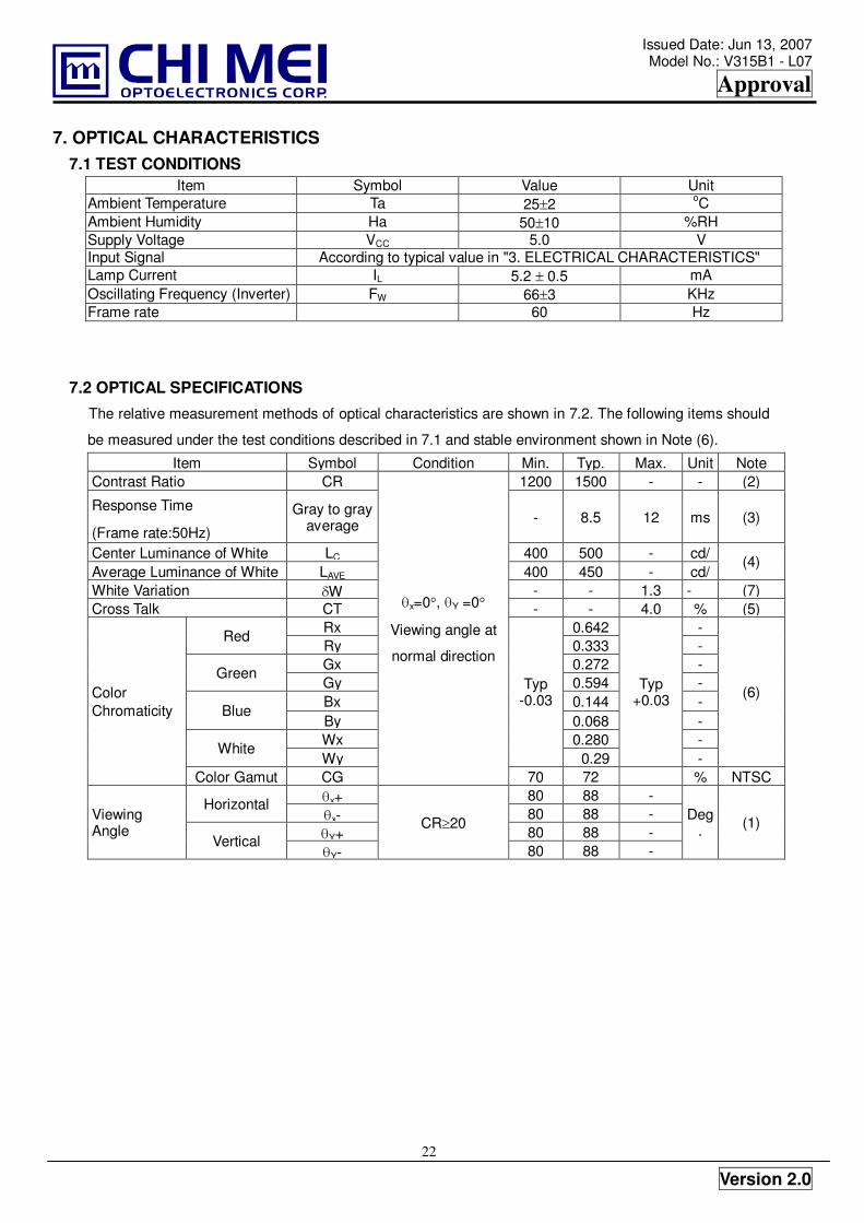
7. OPTICAL CHARACTERISTICS 7.1 TEST CONDITIONS
Item Symbol Value Unit Ambient Temperature Ta 25±2 oC Ambient Humidity Ha 50±10 %RH Supply Voltage VCC 5.0 V Input Signal According to typical value in "3. ELECTRICAL CHARACTERISTICS" Lamp Current IL 5.2 ± 0.5 mA Oscillating Frequency (Inverter) FW 66±3 KHz Frame rate 60 Hz
7.2 OPTICAL SPECIFICATIONS
The relative measurement methods of optical characteristics are shown in 7.2. The following items should
be measured under the test conditions described in 7.1 and stable environment shown in Note (6).
Item Symbol Condition Min. Typ. Max. Unit Note Contrast Ratio CR 1200 1500 - - (2)
Response Time
(Frame rate:50Hz)
Gray to gray average - 8.5 12 ms (3)
Center Luminance of White LC 400 500 - cd/2
Average Luminance of White LAVE 400 450 - cd/2
(4)
White Variation δW - - 1.3 - (7) Cross Talk CT - - 4.0 % (5)
Rx 0.642 - Red Ry 0.333 - Gx 0.272 - Green Gy 0.594 - Bx 0.144 -
Blue By 0.068 - Wx 0.280 - White Wy
Typ -0.03
0.29
Typ +0.03
-
(6) Color Chromaticity
Color Gamut CG
θx=0°, θY =0°
Viewing angle at
normal direction
70 72 % NTSC θx+ 80 88 - Horizontal θx- 80 88 - θY+ 80 88 -
Viewing Angle
Vertical θY-
CR≥20
80 88 -
Deg. (1)
Issued Date: Jun 13, 2007 Model No.: V315B1 - L07
Approval
Version 2.0
23
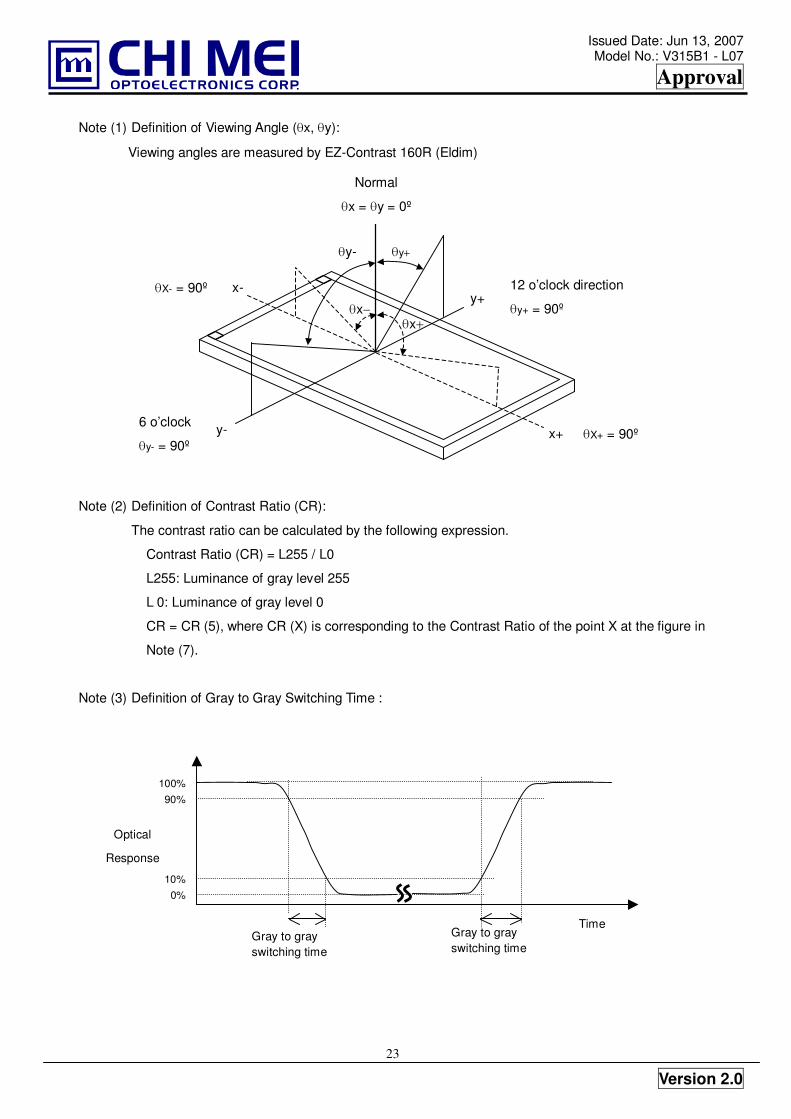
Note (1) Definition of Viewing Angle (θx, θy):
Viewing angles are measured by EZ-Contrast 160R (Eldim)
Note (2) Definition of Contrast Ratio (CR):
The contrast ratio can be calculated by the following expression.
Contrast Ratio (CR) = L255 / L0
L255: Luminance of gray level 255
L 0: Luminance of gray level 0
CR = CR (5), where CR (X) is corresponding to the Contrast Ratio of the point X at the figure in
Note (7).
Note (3) Definition of Gray to Gray Switching Time :
12 o’clock direction
θy+ = 90º
6 o’clock
θy- = 90º
θx− θx+
θy- θy+
x- y+
y- x+
Normal
θx = θy = 0º
θX+ = 90º
θX- = 90º
Optical
Response
100%90%
10%0%
Gray to gray switching time
Time Gray to gray switching time
Issued Date: Jun 13, 2007 Model No.: V315B1 - L07
Approval
Version 2.0
24
The driving signal means the signal of gray level 0, 63, 127, 191, 255.
Gray to gray average time means the average switching time of gray level 0 ,63,127,191,255 to each
other .
Note (4) Definition of Luminance of White (LC, LAVE):
Measure the luminance of gray level 255 at center point and 5 points
LC = L (5)
LAVE = [L (1)+ L (2)+ L (3)+ L (4)+ L (5)] / 5
where L (x) is corresponding to the luminance of the point X at the figure in Note (7).
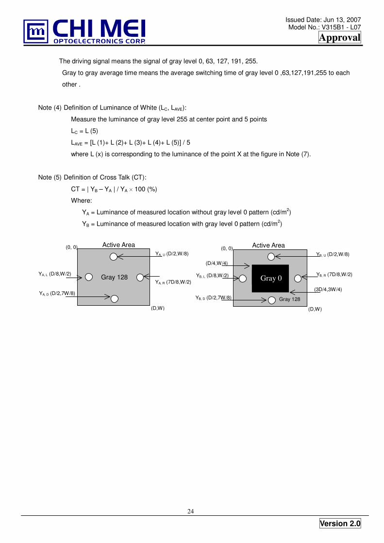
Note (5) Definition of Cross Talk (CT):
CT = | YB – YA | / YA × 100 (%)
Where:
YA = Luminance of measured location without gray level 0 pattern (cd/m2)
YB = Luminance of measured location with gray level 0 pattern (cd/m2)
Active Area YA, U (D/2,W/8)
YA, R (7D/8,W/2)
YA, D (D/2,7W/8)
YA, L (D/8,W/2)
(0, 0)
(D,W)
Gray 128
Active Area
Gray 0
(D/4,W/4)
(3D/4,3W/4)
(0, 0) YB, U (D/2,W/8)
YB, R (7D/8,W/2)
YB, D (D/2,7W/8)
YB, L (D/8,W/2)
(D,W)
Gray 128
Gray 0
Issued Date: Jun 13, 2007 Model No.: V315B1 - L07
Approval
Version 2.0
25
Note (6) Measurement Setup:
The LCD module should be stabilized at given temperature for 1 hour to avoid abrupt temperature
change during measuring. In order to stabilize the luminance, the measurement should be
executed after lighting Backlight for 1 hour in a windless room.
Note (7) Definition of White Variation (δW):
Measure the luminance of gray level 255 at 5 points
δW = Maximum [L (1), L (2), L (3), L (4), L (5)] / Minimum [L (1), L (2), L (3), L (4), L (5)]
D
W
Active Area
Vert
ical
Lin
e
Horizontal Line
: Test Point
X=1 to 5
5
1 2
3 4
D/4 D/2 3D/4
W/4
W/2
3W/4
X
LCD Module
LCD Panel
Center of the Screen Display Color Analyzer (Minolta CA210)
Light Shield Room
(Ambient Luminance < 2 lux)
Issued Date: Jun 13, 2007 Model No.: V315B1 - L07
Approval
Version 2.0
26
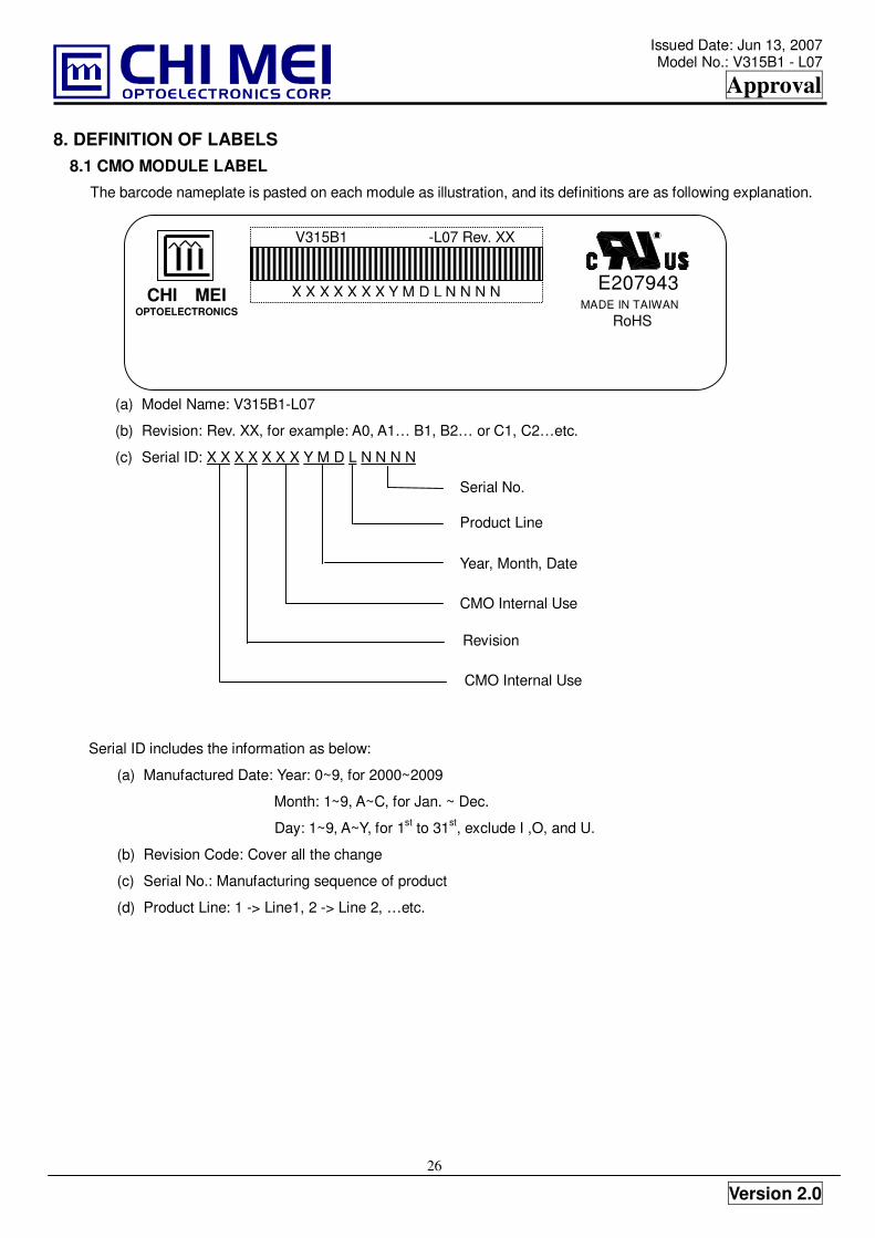
8. DEFINITION OF LABELS 8.1 CMO MODULE LABEL
The barcode nameplate is pasted on each module as illustration, and its definitions are as following explanation.
(a) Model Name: V315B1-L07
(b) Revision: Rev. XX, for example: A0, A1… B1, B2… or C1, C2…etc.
(c) Serial ID: X X X X X X X Y M D L N N N N
Serial ID includes the information as below:
(a) Manufactured Date: Year: 0~9, for 2000~2009
Month: 1~9, A~C, for Jan. ~ Dec.
Day: 1~9, A~Y, for 1st to 31st, exclude I ,O, and U.
(b) Revision Code: Cover all the change
(c) Serial No.: Manufacturing sequence of product
(d) Product Line: 1 -> Line1, 2 -> Line 2, …etc.
Product Line
Year, Month, Date
CMO Internal Use
Revision
CMO Internal Use
Serial No.
CHI MEI OPTOELECTRONICS
X X X X X X X Y M D L N N N N
V315B1 -L07 Rev. XX
MADE IN TAIWAN
E207943
RoHS
Issued Date: Jun 13, 2007 Model No.: V315B1 - L07
Approval
Version 2.0
27
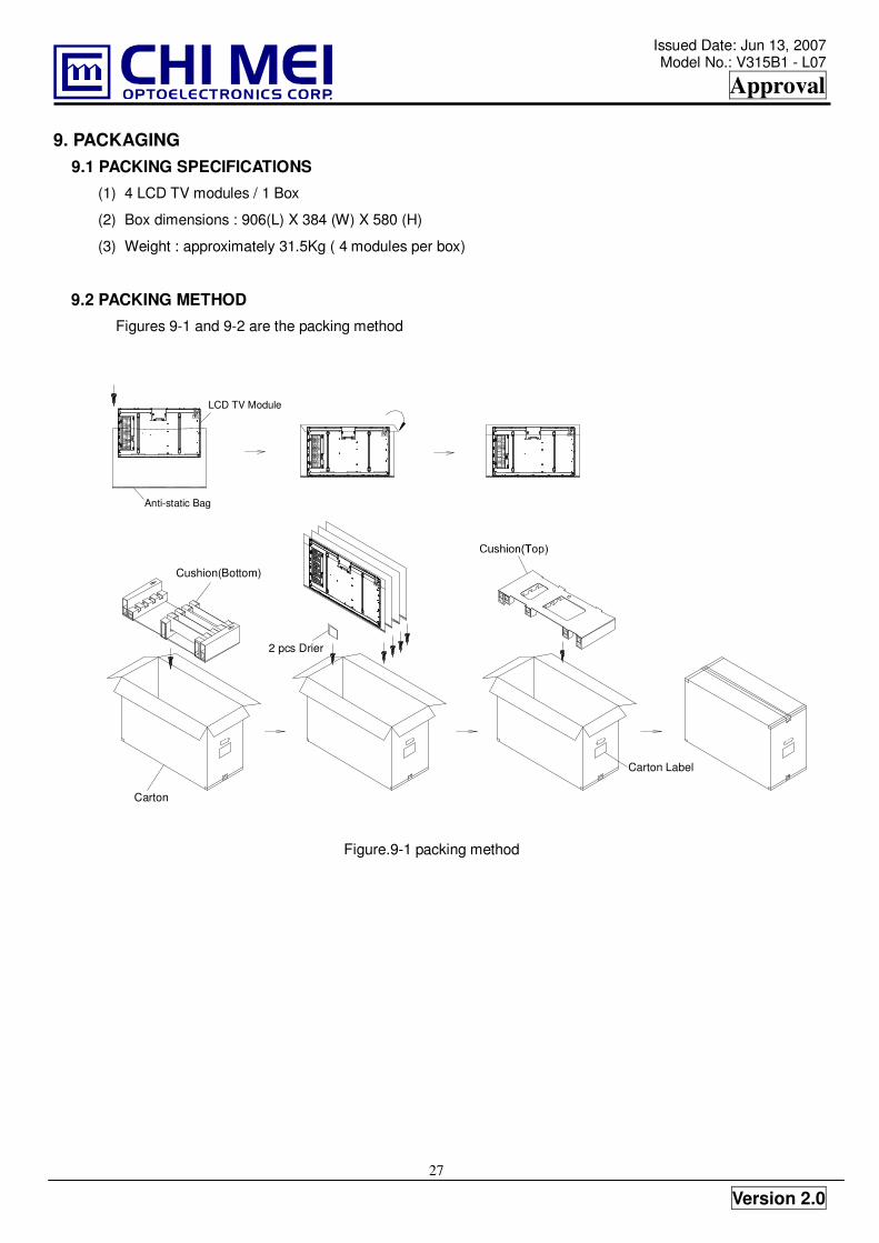
9. PACKAGING 9.1 PACKING SPECIFICATIONS
(1) 4 LCD TV modules / 1 Box
(2) Box dimensions : 906(L) X 384 (W) X 580 (H)
(3) Weight : approximately 31.5Kg ( 4 modules per box)
9.2 PACKING METHOD
Figures 9-1 and 9-2 are the packing method
LCD TV Module
Anti-static Bag
Carton
Carton Label
Cushion(Bottom)
2 pcs Drier
Figure.9-1 packing method
Issued Date: Jun 13, 2007 Model No.: V315B1 - L07
Approval
Version 2.0
28
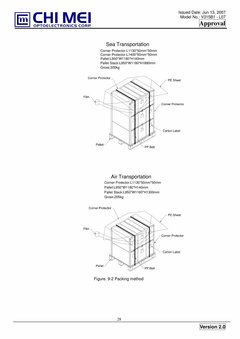
Air Transportation
Sea Transportation
PP Belt
Carton Label
Corner Protector:L1130*50mm*50mm
Gross:300kgPallet Stack:L950*W1180*H1880mmPallet:L950*W1180*H140mmCorner Protector:L1400*50mm*50mm
Gross:205kg
Corner Protector:L1130*50mm*50mm
Pallet Stack:L950*W1180*H1300mmPallet:L950*W1180*H140mm
PE Sheet
PE Sheet
Carton Label
PP Belt
Figure. 9-2 Packing method
Issued Date: Jun 13, 2007 Model No.: V315B1 - L07
Approval
Version 2.0
29
10. PRECAUTIONS 10.1 ASSEMBLY AND HANDLING PRECAUTIONS
(1) Do not apply rough force such as bending or twisting to the module during assembly.
(2) It is recommended to assemble or to install a module into the user’s system in clean working areas.
The dust and oil may cause electrical short or worsen the polarizer.
(3) Do not apply pressure or impulse to the module to prevent the damage of LCD panel and backlight.
(4) Always follow the correct power-on sequence when the LCD module is turned on. This can prevent the
damage and latch-up of the CMOS LSI chips.
(5) Do not plug in or pull out the I/F connector while the module is in operation.
(6) Do not disassemble the module.
(7) Use a soft dry cloth without chemicals for cleaning, because the surface of polarizer is very soft and
easily scratched.
(8) Moisture can easily penetrate into LCD module and may cause the damage during operation.
(9) High temperature or humidity may deteriorate the performance of LCD module. Please store LCD
modules in the specified storage conditions.
(10) When ambient temperature is lower than 10ºC, the display quality might be reduced. For example, the
response time will become slow, and the starting voltage of CCFL will be higher than that of room
temperature.
10.2 SAFETY PRECAUTIONS
(1) The startup voltage of a backlight is over 1000 Volts. It may cause an electrical shock while assembling
with the inverter. Do not disassemble the module or insert anything into the backlight unit.
(2) If the liquid crystal material leaks from the panel, it should be kept away from the eyes or mouth. In
case of contact with hands, skin or clothes, it has to be washed away thoroughly with soap.
(3) After the module’s end of life, it is not harmful in case of normal operation and storage.
11. REGULATORY STANDARDS 11.1 SAFETY
Regulatory Item Standard
UL UL 60950-1: 2003
cUL CAN/CSA C22.2 No.60950-1-03 Information Technology equipment
CB IEC 60950-1:2001
UL UL 60065: 2003
cUL CAN/CSA C22.2 No.60065-03 Audio/Video Apparatus
CB IEC 60065:2001
Issued Date: Jun 13, 2007 Model No.: V315B1 - L07
Approval
Version 2.0
30
12. MECHANICAL CHARACTERISTICS
CHI MEI
��
��
��
��
Issued Date: Jun 13, 2007 Model No.: V315B1 - L07
Approval
Version 2.0
31
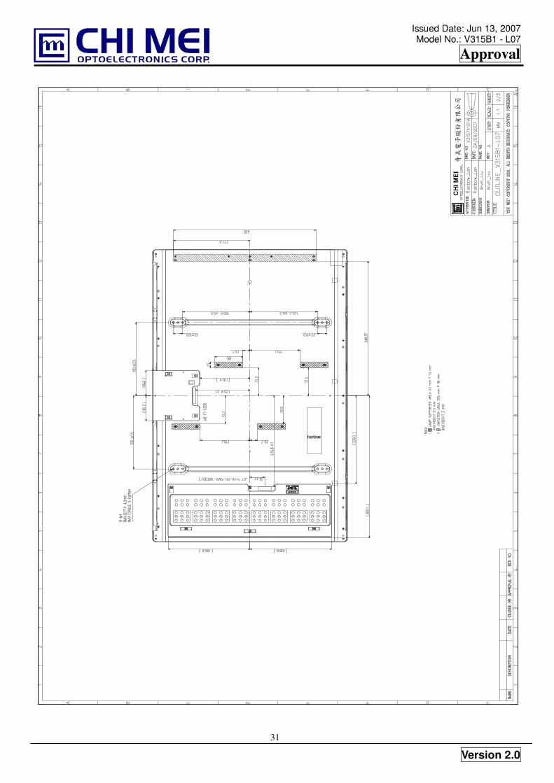
CHI MEI
��
��
��
��
Issued Date: Jun 13, 2007 Model No.: V315B1 - L07
Approval
Version 2.0
32
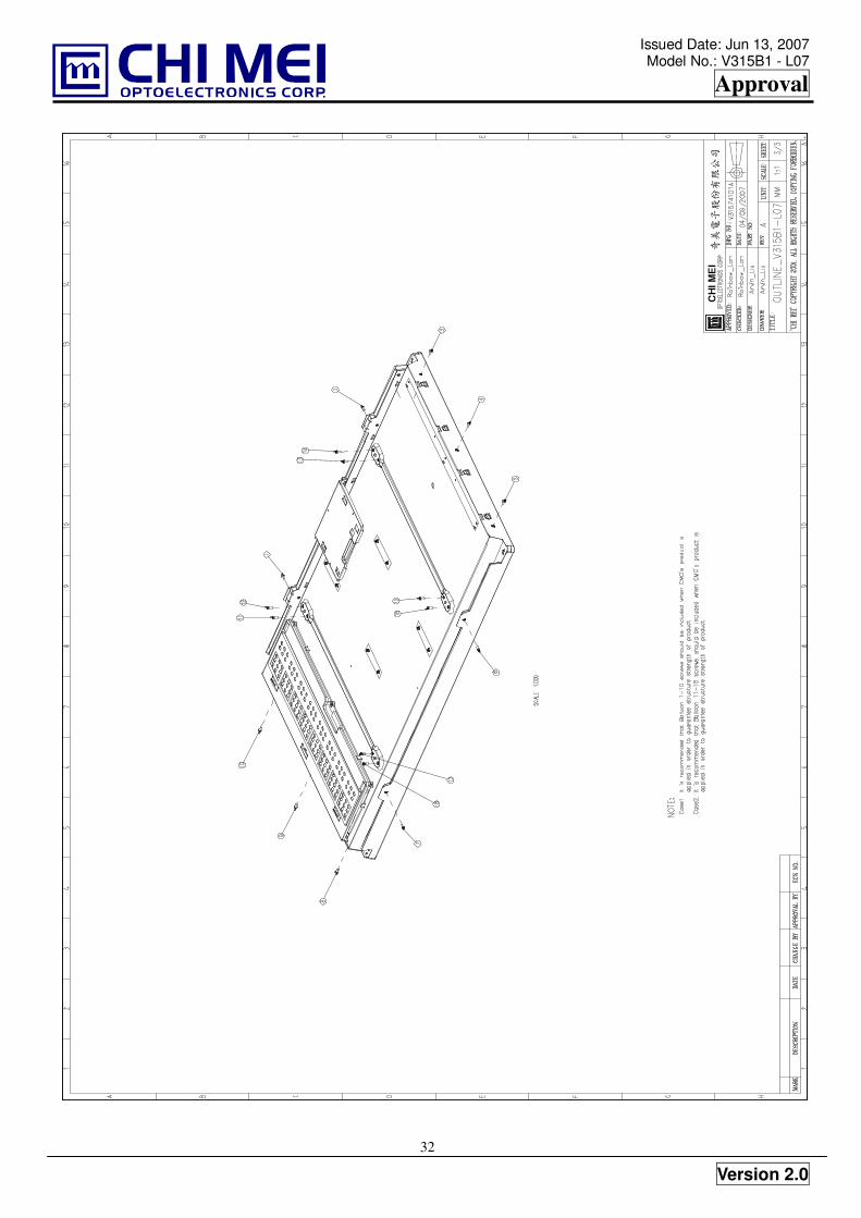
CHI MEI
��
��
��
��