Embed Size (px)
Citation preview

User’sManual
Yokogawa Electric Corporation
Model 701923PBD2000 Differential Probe
IM 701923-01E1st Edition

iIM 701923-01E
ForewordThank you for purchasing the PBD2000 Differentil Probe (Model 701923).
This user’s manual contains useful information about the functions and
operating procedures of the PBD2000 Differentil Probe and lists the handling
precautions of the instrument. To ensure correct use, please read this manual
thoroughly before beginning operation.
After reading this manual, keep it in a convenient location for quick reference in
the event a question arises during operation.
Revisions1st Edition: November 2005
1st Edition : November 2005 (YK)All Rights Reserved, Copyright © 2005 Yokogawa Electric Corporation

ii IM 701923-01E
The following safety markings are used in this manual. 5Improper handling or use can lead to injury to the user or
damage to the instrument. This symbol appears on the
instrument to indicate that the user must refer to the user’s
manual for special instructions. The same symbol appears
in the corresponding place in the user’s manual to identify
those instructions. In the manual, the symbol is used in
conjunction with the word “WARNING”or “CAUTION.”
WARNING Calls attention to actions or conditions that could cause
serious injury or death to the user, and precautions that can
be taken to prevent such occurrences.
CAUTION Calls attentions to actions or conditions that could cause
light injury to the user or damage to the instrument or user’s
data, and precautions that can be taken to prevent such
occurrences.
Note Calls attention to information that is important for proper
operation of the instrument.
Checking the Contents of the PackageIf any of the contents are incorrect, missing, or appear to be abnormal, please
contact your Yokogawa dealer or representative.
PBD2000 Differentil Probe: 1
Various kinds of attachments (see page 1-2)
• Straight and angle pins: 8 each
• Spring type straight and angle pins: 4 each
• Microclips (red and black): 1 each
• Lead wires (red and black): 1 each
• L-pins: 2
• Driver: 1
User’s manual (this manual): 1
Carrying case: 1
Optional Accessories (Sold Separately)Name Model RemarksStandard accessory kit 701915 Set of attachments (the quantity of each
attachment differs from the accessories).

iiiIM 701923-01E
Safety Symbols and PrecautionsTo ensure safe and correct operation of the instrument, you must take the
safety precautions given on the next page. The instrument may not function if
used in a manner not described in this manual. Yokogawa bears no
responsibility for, nor implies any warranty against damages occurring as a
result of failure to take these precautions.
The following safety symbols and words are used in this manual.
Warning: Handle with care. Refer to the user’s manual. This symbol
appears on dangerous locations on the instrument which require special
instructions for proper handling or use. The same symbol appears in the
corresponding place in the manual to identify those instructions.)

iv IM 701923-01E
Safety PrecautionsFor safe use of the instrument, and for best results, please heed the following
warnings and cautions.
WARNING• Take care to avoid electric shock when connecting the probe to the item
under test.• Never disconnect the probe from the measuring instrument while the
probe is connected to the circuit under test.• Never use the probe with wet hands, or when the probe itself is wet.
Electric shock can result.• Before connecting the probe input terminal to the item under test, check
that the measuring instrument is properly grounded, and that the probeoutput connector is connected to the input connector of the oscilloscope.
• Ground the measuring instrument.Always connect the main instrument’s protective grounding.
• Maintain nondestructive input voltages.Do not apply a voltage exceeding [PM]25 V (DC+ACpeak) between inputand ground.
• Do not use the probe in humid locationsTo avoid electric shock, never use the probe in areas of high humidity.
• Do not use the probe near flammable gases.To avoid injury and fire, do not use the probe near flammable orexplosive gasses or vapors.
• Avoid exposed circuits.To prevent injury, remove all jewelry such as rings and wristwatches.When the power is ON, do not touch any exposed contact points orcomponents.
CAUTION• The probe head has undergone a precision assembly process. Take
sufficient care when handling the probe as sudden changes in ambienttemperature and physical shocks can damage it.
• Do not inadvertently twist or pull the cable. The wires inside the cablecan break, causing malfunction.
• Avoid vibration, shock, and static electricity during shipping andhandling. Take extra care not to drop the probe.
• Avoid storing or using the probe in direct sunlight, or in areas with hightemperature, humidity, or condensation. Deformation and deteriorationof insulation can occur resulting in failure to retain product specifications.
• Inspect the probe before use to ensure that damage has not occurredduring shipping and storing. If damage is found, contact your nearestYokogawa dealer or sales representative.
• This probe is not water or dust resistant. Do not use the probe in areaswith a lot of dust, or near water.

vIM 701923-01E
Contents
Foreword ................................................................................................... iChecking the Contents of the Package .................................................... iiSafety Symbols and Precautions ............................................................ iiiSafety Precautions .................................................................................. iv
Product Overview .....................................................................................1Features .................................................................................................. 1Names of Parts .........................................................................................2Operating Procedures ............................................................................. 3Product Specifications ............................................................................. 5

1IM 701923-01E
Product OverviewThe PBD2000 Differential Probe is a 2 GHz bandwidth differential input probe
that can be used in combination with DL9000 series digital oscilloscopes. The
probe is simply connected to the BNC input terminal on the DL9000 series
instrument. By touching the probe tip to the circuit under test, you can view
voltage waveforms.
Features• Allows direct observation of differential signals
• Common mode rejection capability
• Wide frequency bandwidth (DC to 2 GHz)
• Power can be supplied to the probe from the DL9000 series instrument.
• The probe is automatically recognized by the DL9000 series instrument.
• The attachment that touches the circuit under test can be changed
• Compact and lightweight

2 IM 701923-01E
Names of Parts
Probe headCable
Probe interface
Add various attachments, connect to circuit under test
To digital oscilloscope input
Latch release lever
Output terminal
Cable Probe head
Probe interfaceInterface spring pin
L-pins (2)Lead wires (one each in red and black) Microclips
Straight pins (8)
Angle pins (8)
Spring type straight pins (4)
Spring type angle pins (4)
Connect to probe head
(one each in red and black)
The quantity in parentheses ( ) is the number of the various attachments that belong to a single probe.
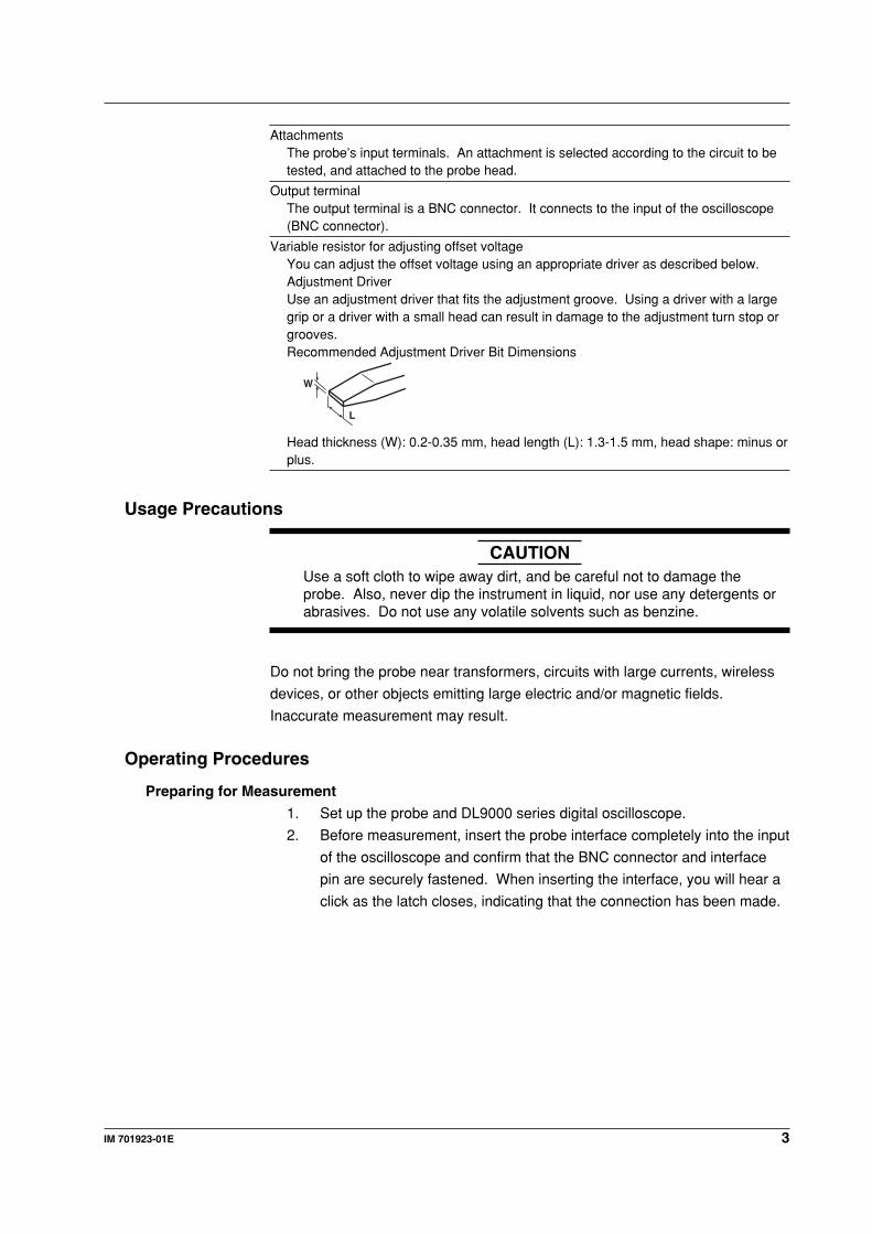
Attachments
Variable Resistor for Adjusting Offset Voltage
Probe interfaceThe point of connection to the input of the digital oscilloscope.
Interface spring pinWhen the probe output terminal is connected, it touches the pad on the interfaceboard of the oscilloscope. The probe’s power is supplied through this interfacecomponent. The interface also supplies the offset voltage, and allows automaticrecognition of the probe.
CableLinks the probe interface and probe head.
Probe headContacts the circuit under test through various attachments.
Latch release leverA lever that releases the lock connecting the probe output terminal to the oscilloscopeinput.
3IM 701923-01E
AttachmentsThe probe’s input terminals. An attachment is selected according to the circuit to betested, and attached to the probe head.
Output terminalThe output terminal is a BNC connector. It connects to the input of the oscilloscope(BNC connector).
Variable resistor for adjusting offset voltageYou can adjust the offset voltage using an appropriate driver as described below.Adjustment DriverUse an adjustment driver that fits the adjustment groove. Using a driver with a largegrip or a driver with a small head can result in damage to the adjustment turn stop orgrooves.Recommended Adjustment Driver Bit Dimensions
L
W
Head thickness (W): 0.2-0.35 mm, head length (L): 1.3-1.5 mm, head shape: minus orplus.
Usage Precautions
CAUTIONUse a soft cloth to wipe away dirt, and be careful not to damage theprobe. Also, never dip the instrument in liquid, nor use any detergents orabrasives. Do not use any volatile solvents such as benzine.
Do not bring the probe near transformers, circuits with large currents, wireless
devices, or other objects emitting large electric and/or magnetic fields.
Inaccurate measurement may result.
Operating Procedures
Preparing for Measurement
1. Set up the probe and DL9000 series digital oscilloscope.
2. Before measurement, insert the probe interface completely into the input
of the oscilloscope and confirm that the BNC connector and interface
pin are securely fastened. When inserting the interface, you will hear a
click as the latch closes, indicating that the connection has been made.

4 IM 701923-01E
Handling the Attachments
You can change attachments according to the circuit to be tested.
As in the figure below, there is a hole for attaching the attachments to the tip of
the probe head.
+
-
Plus side signal input terminal (noninverted)
Minus side signal input terminal (inverted)
There are straight and angle pins. Select an attachment according to the circuit
to be tested.
Since the impedance of the probe input is high, the inductance from the probe
head to the circuit under test has a large effect on measured results of high
frequency signal components. When measuring signals including frequency
components of 100 MHz and higher in particular, we recommend that you use
as short of an attachment as possible to connect the circuit under test to the
probe head (both signal input terminal and ground terminal).
Example
Lead wire
Microclips
• For signals of relatively low frequency
Probe head
• For signals of relatively high frequency
Select an attachment according to the circuit to be tested (straight pin, angle pin, spring type straight pin, spring type angle pin).

5IM 701923-01E
Warm-up/offset adjustmentWarm-up
After connecting the probe, heat emitted from the probe itself causes the offset
voltage to drift. The probe should nearly stabilize about thirty minutes after
applying power. Allow a thirty minute warm-up after connecting the probe.
Offset adjustment
You can turn the offset voltage adjustment variable resistor on the probe
interface with the appropriate adjustment driver (see page 3) to adjust the offset
voltage remaining after warm-up (residual offset voltage).
CAUTIONWhen adjusting the offset voltage, do not force the offset voltageadjustment variable resistor. The offset voltage adjustment variableresistor may break.
Note• The offset voltage drifts as a result of the ambient temperature. During continuous
use, make sure the ambient temperature is stable.• Do not use the offset voltage adjustment variable resistor for any purpose other
than adjusting the residual offset voltage. If you use it for purposes such as
deliberately changing the offset value, the instrument will fail to meet itsspecifications.
6 IM 701923-01E
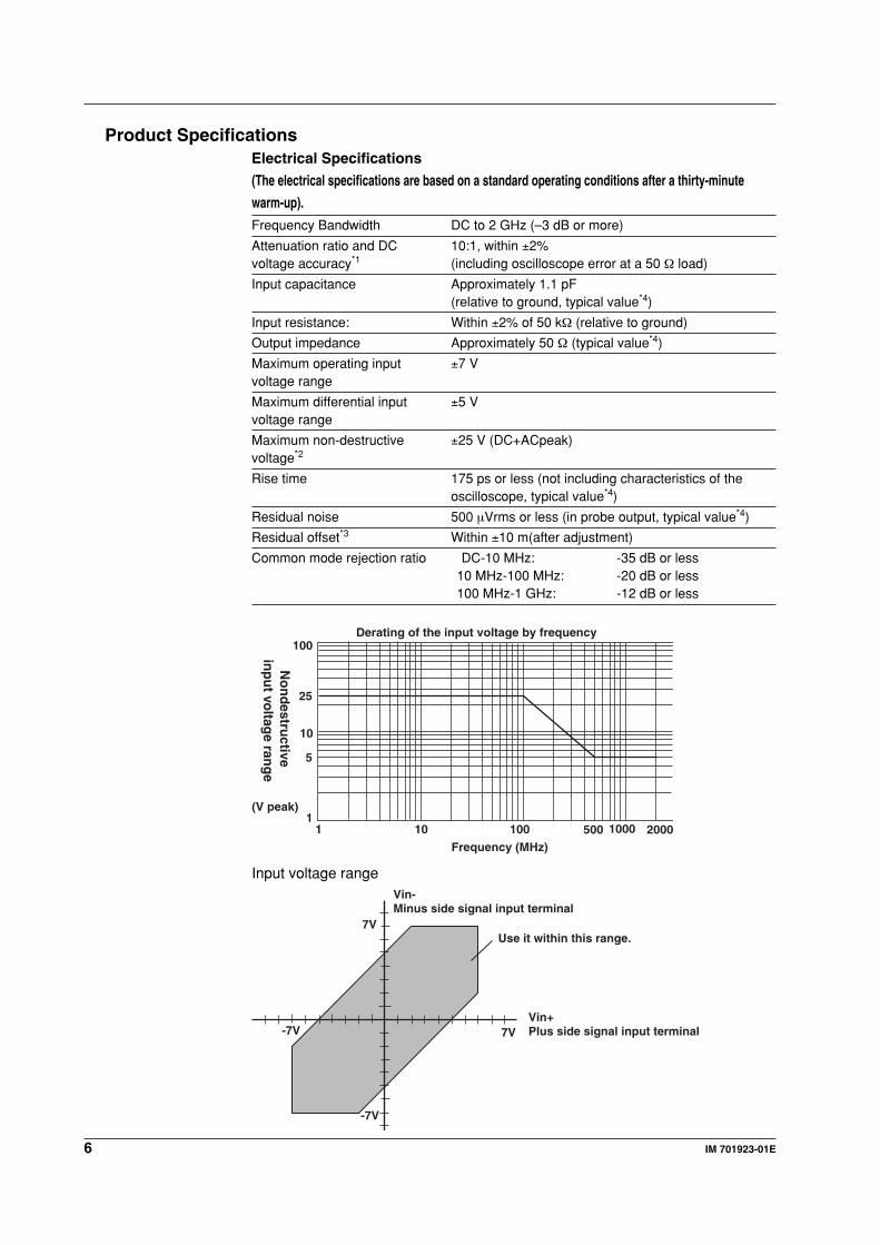
Product SpecificationsElectrical Specifications
(The electrical specifications are based on a standard operating conditions after a thirty-minute
warm-up).
Frequency Bandwidth DC to 2 GHz (–3 dB or more)
Attenuation ratio and DC 10:1, within ±2%voltage accuracy*1 (including oscilloscope error at a 50 Ω load)
Input capacitance Approximately 1.1 pF(relative to ground, typical value*4)
Input resistance: Within ±2% of 50 kΩ (relative to ground)
Output impedance Approximately 50 Ω (typical value*4)
Maximum operating input ±7 Vvoltage range
Maximum differential input ±5 Vvoltage range
Maximum non-destructive ±25 V (DC+ACpeak)voltage*2
Rise time 175 ps or less (not including characteristics of theoscilloscope, typical value*4)
Residual noise 500 µVrms or less (in probe output, typical value*4)
Residual offset*3 Within ±10 m(after adjustment)
Common mode rejection ratio DC-10 MHz: -35 dB or less10 MHz-100 MHz: -20 dB or less100 MHz-1 GHz: -12 dB or less
1 10 100 10001
10
100
25
Frequency (MHz)
Derating of the input voltage by frequency
(V peak)
500 2000
5
No
nd
estructive
inp
ut vo
ltage ran
ge
Input voltage range
Use it within this range.
Vin+Plus side signal input terminal
Vin-Minus side signal input terminal
7V-7V
7V
-7V

7IM 701923-01E
General Specifications
Power range Standard power supply voltage of ±5 V, within ±5%Interface (The probe is supplied power from a dedicated
terminal. Connect the probe to a DL series instrumenthaving a matching dedicated terminal.)
Storage altitude 3,000 m or less
Operating altitude 2,000 m or less
Standard operating environment Temperature range 23°C±5°CHumidity range*5 55%±10%RH
Operating environment Temperature range 5°C to 40°CHumidity range*5 20 to 80%RH
Storage environment Temperature range –20 to 60°CHumidity range*5 20 to 80%RH
Calibration cycle 1 year
Warm-up time 30 minutes or more
Total length Approximately 1.2 m.
Weight Approximately 80 g.
Standards Conformance
EMC Emission Conforms to EN61326 Class AImmunity Conforms to EN61326 standards
Effect of Immunity Environmentnoise increase: within ± 2 V*6
*1 Excluding residual offset voltage*2 Nondestructive maximum input voltage. This is not the dynamic range of the probe.*3 When 0 V are input to both the plus and minus side signal input terminals.*4 Typical value represents a typical or average value. It is not strictly guaranteed.*5 No condensation*6 Test conditions
Frequency bandwidth limit 20 MHz, using a DL9000 series digital oscilloscope set foran input impedance of 50 Ω, and both plus and minus probe tip inputs connected(terminated) at 50 Ω.

App-1IM 701923-01E
Appendix (High Speed Waveform Measurement and Probing)The speed of devices and electronic circuits incorporated into a variety of
instruments, including digital home electronics, is increasing and the
oscilloscopes and probes used to observe their signal waveforms are also
faster and have wider bandwidths.
When the speed of the measured signal increases, there are cases when
correct measurements cannot be taken due to problems that have never
occurred before, especially in probing. In this article I offer some hints regarding
the accurate probing of high speed signals.
Types of Voltage Probe
A Voltage probes is a type of voltage sensor. The ideal probe should be
selected according to the signal's voltage, output impedance, frequency
components, and other factors. Individual probes have their own particular pros
and cons, and since the input impedance (resistance and capacitance) and
frequency can differ greatly depending on the type of probe, it is essential to
understand the characteristics of the available probes in order to obtain highly
reliable measurements. Below are three examples of probes generally used for
measurements on high frequency circuits.
Passive Probes
Passive probes with a 10:1 attenuation ratio are the most widely used due to
their low cost, ruggedness, high withstand voltage, and high input impedance at
DC and low frequencies. Yokogawa's standard 10:1 passive probes are easy-
to-use for general applications. They have an input impedance of 10 M_, an
input capacitance of approximately 14 pF and a withstand voltage of 600 V.
However the 14 pF input capacitance might cause problems when high
frequencies are measured.
PB500
500 MHz Passive Probe
(to use with DL9000 Series)

App-2 IM 701923-01E
Active Probes / FET Probes
Active and FET probes are those most often used to measure high frequency
signals. Unlike passive probes, an impedance converting buffer amplifier is
situated near the tip of the probe which enables them to handle higher
frequencies with around 1 pF input capacitance. They require a power supply
and must be handled with more care than a passive probe since the with-stand
voltage is lower. They are very effective in terms of reliability and their ability to
reproduce high frequency signal waveforms.
PBA25002.5 GHz Active Probe(to use with DL9000 Series)
Low Capacitance Probes (Resistance)
These probes are not so well known, but they have been used with measuring
instruments having 50 Ω inputs for a relatively long time. The probe head has a
special built-in 450 Ω or 950 Ω resistor, designed for high frequency, and uses a
50 Ω coaxial cable. It is still very popular to this day since the input capacitance
is extremely small. As the input resistance is 500 Ω or 1 kΩ it can have an affect
on the DC bias or output amplitude if the impedance of the signal source being
measured is high. However, this probe is ideal for high quality measurement of
clock edges or other high speed digital signal waveforms as the input
capacitance is half, or even a small fraction, of that of the active probe.
PBL50005 GHz Low Capacitance Probe

App-3IM 701923-01E
Problems with Probing High Speed SignalsThe Loading EffectWhen a probe is connected to the circuit under test, the input impedance of theprobe itself has certain effects on the circuit. This is called the loading effect.For example, when measuring a feedback circuit, the phase of the circuitchanges due to the impedance of the connected probe, thus changing theoperation of the circuit. For oscillating circuits, the frequency of oscillation canchange or the oscillation can stop altogether. Special care must be taken whenselecting a probe for measuring circuits that are sensitive to capacitance.
Observational Bandwidth Limits due to Probe Input CapacitanceThere can be cases where there are notable low pass filter effects related to thesignal source impedance and the probe's load capacitance particularly whenobserving frequency components of 100 MHz or more.Let us take an example of a 50 Ω circuit (see below). In this example, theequivalent signal source impedance can be seen as 25 Ω (2 x 50 Ω in parallel)when observing the signal waveform at the load (terminal), and the cutofffrequency at the probe's input point is fc=1/2 π RC if the probe inputcapacitance is added. When using a passive probe with an input capacitance of14 pF, fc equals 455 MHz, but when a 0.9 pF input capacitance active probe isused, fc equals 7 GHz.It is preferable to use an active or FET probe with a smaller input capacitancebecause even more pronounced loading effects emerge when measuring a
circuit with a high output impedance.
RS=50Ω
ZO=50Ω RL=50Ω
Probe
Signalsource
Resonance due to InductancePins or wires of one sort or another are used to connect the probe to the circuitunder test. Inductance occurs when these pins or wires reach certain lengths,which results in resonance with the probe's input capacitance. This will notobscure observation of the waveform if these resonant frequencies are outsideof the oscilloscope's frequency bandwidth, but overshooting or ringing, whichwas not originally present, is introduced into the signal waveform beingobserved when the inductance or capacitance is large. The resonant frequencyis surprisingly low when the resonant frequencies of three different types ofprobes are compared as in Figure 1 with a given connected inductance of 10nH (a length of up to 1-2 cm). The user must be aware that effects of thisinductance can be found not only on the probe input, but also in the ground
connection.
PB500 PBA2500 PBL5000Passive Probe Active Probe Low Capacitance Probe
Input Impedance Approx 14 pF Approx 0.9 pF Approx 0.25 pF or 0.4 pFResonant Frequency 425 MHz 1.68 GHz 3.18 GHz(When L=10 nH)

App-4 IM 701923-01E
Changes in Cable Characteristics
A coaxial cable is used to transfer signals from the probe tip to the oscilloscope.
Cables that can offer the right balance of both flexibility and high frequency
performance are selected after considering the ways in which the cables will
actually be handled. Even so, if a cable is bent sharply, the dielectric can break,
altering the characteristic impedance and subsequently weakening the cable's
throughput and reflectivity. This in turn will affect the high frequency
components of the observed waveform. This is one of the causes of poor
repeatability in the observation of high frequency waveforms and the
repeatability can be increased by bending the cables as little as possible. When
bending is necessary, please do so in a uniform manner.
Getting the Best Performance Out of Your Probe
When using probes, inductance-based resonance is the biggest problem during
waveform measurement and it is most important to suppress it. Make the
probe's input pins and ground lead as short as possible when the goal is to
easily check signals (browsing). When highly reliable waveform observation is
called for, prepare a thru-hole PCB for connecting the probe and directly
connect the probe's signal input pins onto the PCB track or to another fitting
(No. 1 and No. 2). Connect the probe to a prepared copper wire or plate that is
as thick as possible to reduce inductance in the ground.
If it is simply not possible to connect a short wire, you can insert a 50-100 _
resistor to dampen the resonance (No. 3). In this case, the measurable
frequency bandwidth is reduced by the resistance, but you can approximate the
original waveform more closely by suppressing the resonance effects of
overshooting and ringing.
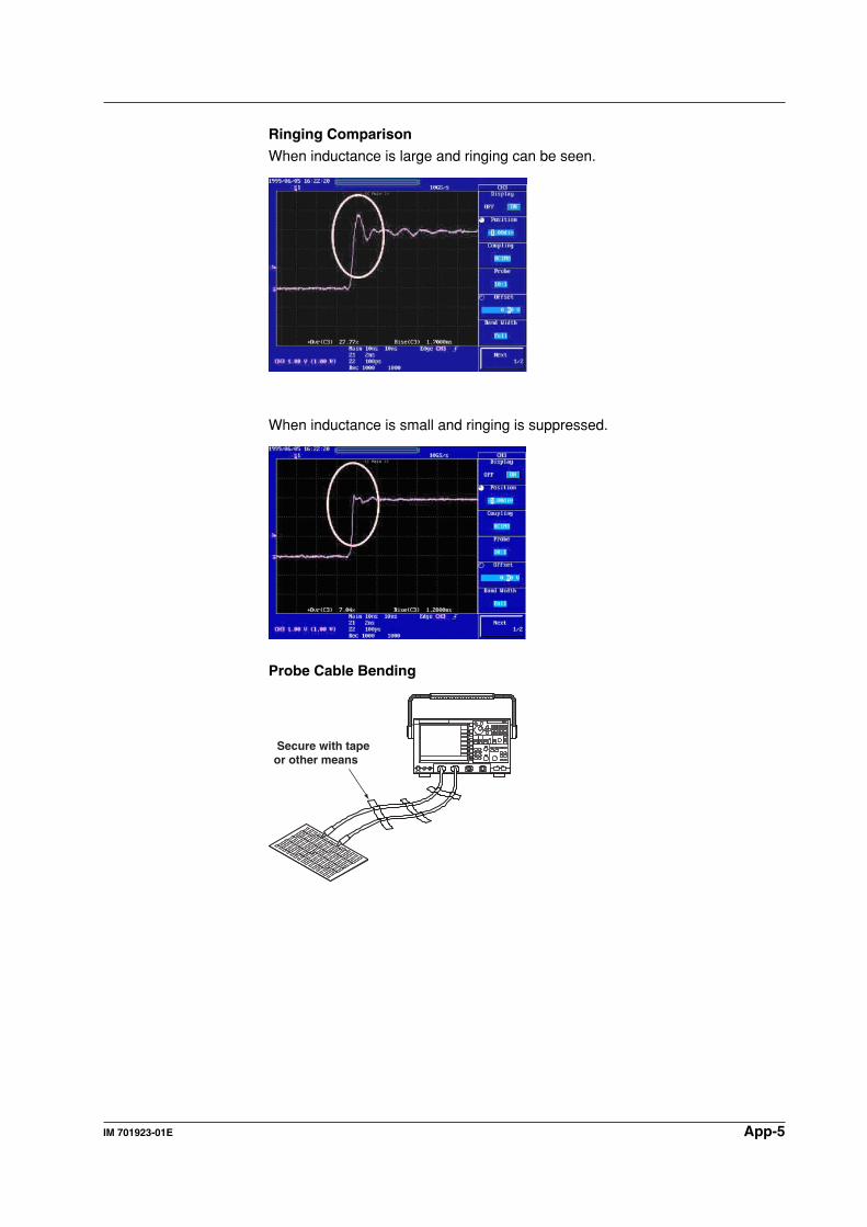
Also, try securing the cable to the workbench with tape so that the bends in the
cable do not change (See the next page) since high frequency signal
components are, as stated above, affected by cable bending. This may improve
the repeatability of the observed waveform.
Ringing Comparison
Registor
PBA2500
ObstacleSolder
PBA2500
Solder a pin in theGND thru-hole
Microstrip line
Peel off the solider resist, then solidera pin
Microstrip line
GND
GND thru-hole
No. 1 No. 2 No. 3
App-5IM 701923-01E
Ringing Comparison
When inductance is large and ringing can be seen.
When inductance is small and ringing is suppressed.
Probe Cable Bending
Secure with tapeor other means