Embed Size (px)
Citation preview
Model 5100C
Service Manual
The circuit schematics herein provided for reference only are not necessarily the latest version.
Mainboard 71-51C00-D02
Specifications are subject to change without notice. Apr. 1999
:

1
TABLE OF CONTENT
ý SPECIFICATIONS ................................................................................................................................3
ý I/O ADDRESS MAP ..............................................................................................................................6
ý SYSTEM MEMORY MAP..................................................................................................................6
ý MOTHERBOARD .................................................................................................................................7
ý MICROPROCESSOR...........................................................................................................................7
ý CHIPS ........................................................................................................................................................8
SOUTHBRIDGE CHIP-INTEL 82371EB (PIIX4E) ...........................................................................................8
VGA CONTROLLER-S3 280 ................................................................................................................................9
PC CARD 95 (CARD BUS) INTERFACE CONTROLLER-TI-1225 ...................................................................10
SUPER I/O FLOPPY DISK CONTROLLER-FDC37N669..................................................................................11
HIGH PERFORMANCE PCI AUDIO CHIP - ES1946.......................................................................................... 12
KEYBOARD CONTROLLER-M38867M8.......................................................................................................... 12
ý DEVICE PORT CONNECTOR DESCRIPTION .......................................................................13
FLOPPY DISK DRIVE & SECONDARY IDE I NTERFACE ..................................................................................13
HARD DISK DRIVE INTERFACE .........................................................................................................................14
SECONDARY MASTER CD-ROM DRIVE INTERFACE .................................................................................... 15
RS-232C SERIAL INTERFACE ...........................................................................................................................16
PARALLEL INTERFACE ........................................................................................................................................16
EXPANSION MEMORY SOCKET .........................................................................................................................17
INTERNAL TRACKPAD INTERFACE .................................................................................................................... 19
EXTERNAL MONITOR INTERFACE .................................................................................................................... 19
EXTERNAL S-VIDEO TV-OUT INTERFACE .......................................................................................................19
EXTERNAL KEYBOARD/PS2 M OUSE INTERFAC.............................................................................................20
EXTERNAL USB (UNIVERSAL SERIAL BUS) INTERFACE ..............................................................................20
PCMCIA CARDBUS INTERFACE......................................................................................................................21
LCD INTERFACE ( FOR XGA TFT).................................................................................................................23
PCI BUS INTERFACE ( FOR MODEM OPTION)............................................................................................... 24
ý DC/DC CONVERTER BOARD .......................................................................................................25
INPUT CHARACTERISTICS ..................................................................................................................................25
EFFICIENCY 25
OUTPUT CHARACTERISTICS..............................................................................................................................25
2
SYSTEM ALARM.................................................................................................................................................25
ý INVERTER BOARD ...........................................................................................................................26
PIN ASSIGNMENT................................................................................................................................................26
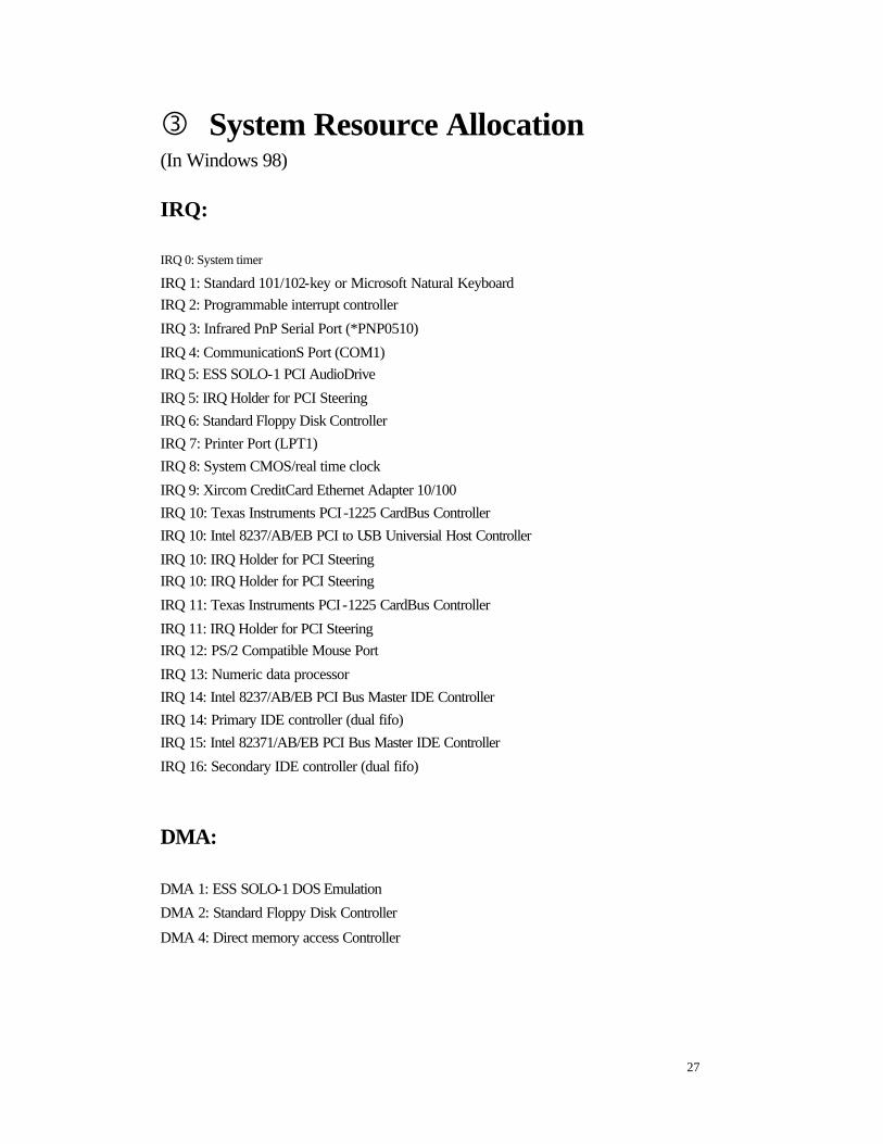
ý SYSTEM RESOURCE ALLOCATION ........................................................................................27
(IN WINDOWS 98) ...........................................................................................................27
IRQ: 27
DMA: 27
ý PARTS LIST.......................................................................................................................................... 28
ý OPTIONAL PARTS .............................................................................................................................41
POWER CORD .................................................................................................................................................41
KEYBOARD......................................................................................................................................................42
3
� SPECIFICATIONS
Processor
� Intel® Celeron™ processors 300A/333/366/400/433 MHz
� Intel® Mobile Pentium® II / Celeron™ processors 266/300/333/366 MHz
Memory
� Two 144pins SODIMM sockets
� Supports EDO/Sync DRAM SODIMM (3.3V)
� 8/16/32/64/128 MB module (optional)
� Expendable memory up to 256MB.
System BIOS
� 256KB Flash ROM
� Systemsoft, Plug and Play 1.0a, ACPI (1.0)
Display
� SVGA flat panel 12.1” TFT
� AGP 1X
� 64-bit hardware 2D/3D Accelerator Graphics Engine
� TV-out with Marco Vision® V7.1 anti-copy technology
� 4MB display memory SGRAM type
� CRT resolution up to 1280x1024x16M
� DuoView™ display capability under Windows 98
� Support Zoomed Video Port
� Support Software MPEG II playback (option).
Storage
� 3.5” 3-mode FDD/12.7mm(h) LS-120
� DVD-ROM (12.7mm)/CD-ROM (24X speed, 12.7mmH or 9.5mmH)
� 2.5” 12.7mm(h) HDD, support LBA mode
� Support Master mode IDE, PIO mode 4/ATA-33 (Ultra DMA)
4
Audio
� 3D stereo sound system
� Compatible Sound-Blaster PRO™ version 3.01
� IIS interface for external ZV port or MPEG audio
� Built-in microphone
� Built-in 2 speakers
� Software Wavetable
� FM music synthesizer 16 bits stereo sound system
PC Card Sockets
� Two type II (PCI) PCMCIA 3.3V/5V sockets
� Support Zoom Video Port (Socket A)/CardBus (PC Card95)
Interface
� Built-in trackpad (PS/2)
� One USB port
� One serial port
� One parallel port (LPT1), support ECP/EPP 1.7a and 1.9
� Infrared file transfer, IrDA 1.0/ASKIR
� External CRT monitor
� One S-Video jack for TV output
� One External keyboard/mouse (PS/2 type) port
� One headphone jack
� One microphone jack
� One RJ-11 jack for Plug & Play Modem Accessory (option)
� DC-in jack
Communication
� Wireless Infrared transfer, IrDA 1.0 compliant
� 56K Plug & Play Modem v.90 compliant (option)
5
Power Management
� Support APM v1.2
� Support ACPI v1.0
� Soft Off by system Power button
� Support suspend to disk
� Battery low suspend
� Resume from alarm time
� Resume from modem ring (COM port only)
Power
� Full range AC adapter – AC in 100-240V, 47-63Hz
� Support one removable Ni-MH/Li-Ion Battery
Size & Weight
� 280mm(w)x240mm(d)x39.5mm(h)
� 2.8kg (with Lithium-Ion battery)
Keyboard
� 84 keys Win95 keyboard include numeric keypad.
Environment
� Temperature:
Operating: 5�C~35�C, Non-Operating: 20�C~60�C
� Humidity
Operating: 20%~80%, Non-Operating: 10%~90%
Optional
� 5001 Ni-MH Battery
� 5002 Li-Ion Battery
� 5002S Smart Li-Ion Battery
� 5003 DVD-ROM Drive Kit
� 5005 LS-120 MB Floppy Drive Kit
� 1008 MPEG playback kit
� 2005 Car Adapter
� 5008 56K v.90 Modem
6
� I/O Address Map
Hex range Device 000 - 00F DMA controller-1 020 - 021 Interrupt controller-1 040 - 043 Timer 1 048 - 04B Timer 2 060 - 06E KB controller M38813 chip select 070 - 071 RTC and NMI mask 080 - 08F DMA page register 0A0 - 0A1 Interrupt controller-2 0C0 - 0DF DMA controller-2 1F0 - 1F7 Fixed disk select 3F6 , 3F7 2F8 - 2FF Serial port 2 378 - 37A Parallel port 1 3B4 , 3B5 CRT controller index (mono) 3D4 , 3D5 CRT controller index (color) 3BA Feature control 3C0 - 3DA 3F2 - 3F7 Floppy disk controller 3F0 , 3F1 configuration port 3F8 - 3FF Serial port 1
� System Memory Map
ADDRESS SIZE FUNCTION 000000 -09FFFF
640KB 640KB Base Memory
0A0000 - 0BFFFF
128KB Video RAM
0C0000 - 0CBFFF
48KB VGA BIOS
0CC000 - 0DFFFF
80KB Reserved
0E0000 - 0EFFFF
64KB System BIOS for SCU,PCI,PnP, PMU
0F0000 - 0FFFFF
64KB System BIOS for Kernal
100000 - 16MB to 256MB Extended Memory
7
� Motherboard
The motherboard is designed with Intel Celeron processor based and includes the following CHIPSET function:
- 82371EB PIIX4E chipset solution from INTEL - 82443ZX Northbridge chipset solution from INTEL - S3 280 AGP 1X Multimedia Flat Panel Controller - TI 1225 PC CARD Controller - EDC37N669 super I/O Floppy Disk Controller - ES1946 PCI Audio Chip - M38867 Keyboard Controller
� Microprocessor The model 5100C is equipped with Intel Celeron processor base. A: Intel Celeron processor 300A/333/366 product line Features:
� P6 core (PPGA package)
� Separate 16K instruction and 16K data level one caches
� Integrated 128K second level cache
� Cachenable 4GB of system memory
� High performances Floating Point Unit
� Enhanced 64 bits data bus
� Dynamic Excution micro-architecture
� MMX media technology instruction
� Power management feature
� Low power GTL+ Host bus specification
B. 443ZX Host Bridge System Controller Intel’s 443ZX Host Bridge system controller is a highly integrated device that combines the processor
bus controller, the DRAM controller, and the PCI bus controller into one component. The 443ZX Host
Bridge has multiple power management features as below:
� Host Interface
� Memory Interface
� PCI Interface
� AGP Interface
8
� Chips
Southbridge Chip-INTEL 82371EB (PIIX4E)
It contains the following features:
� Support Kits for both Pentium and Pentium II Microprocessors
� Multifunction PCI to ISA Bridge
- Support PCI at 33 MHz
- Support PCI Rev 2.1 Specification
- Support Full ISA or Extended I/O BUS
-
� Support Mobile Deep Green Environments
- 3.3V Operation with 5V Tolerant Buffers
- Ultra-low Power for Mobile Environments Support
� Full support for ACPI (Advanced Configuration and Power Interface) Revision 1.0
� Integrated IDE Controller
- Support Ultra DMA/33
� Support two 82C37 Enhanced DMA Controller
� Support two 82C59 Intrrupt Controller
� Support 82C54 Timmer Based
� Support UHCI USB Ports
� Support SMBus
9
VGA Controller-S3 280
The S3 86260 Multimedia Flat Panel Controller is a DRAM based, fully integrated LCD, CRT & TV
64 bits controller for AGP systems. It contains the following functions:
� Support displays for 4MB
� 64bit high performance 2D/3D Graphic Engine
� Support bus master AGP and SGRAM memory
� Support 18 bit TFT panels up to 1024x768 resolution
� Support non-interlaced 1280x1024x64k, 1024x768x16M&16:9(TV OUT), 800x600x16M, and
640x480x16M color on CRT.
� Simultaneous display in 18 bit color on flat panel and CRT
� Internal buffer provides flicker reduction
� S3 86260 DAC can directly interface with a standard off-the-shelf NTSC/PAL encoder.
Composite synchronization signals support standard home TV connection up to 1280x1024x16M
and 16:9 wide mode.
� Graphic functions optimized by a 64-bit internal data bus and VGA, SVGA , and XGA flat panel
� Provide flexible and extensive power management capabilities and support four states of VESA
Display Power Management Signaling standard
� Industry leading DuoView Simul taneous display at Windows 98
� Fully compliant ZV-port interface with device driver support for VPM
� Motion compensation
10
PC Card 95 (Card Bus) Interface Controller-TI-1225
TI Card bus Interface Controller 1225 implements the
PCMCIA 2.0/JEIDA 4.1 standard. It contains the following functions:
� Support 2 PCMCIA 2.1& JEIDA 4.2 R2 cards or 2 CardBus cards
� Yenta Registers-compatible
� Support Zoom Video Mode
� PCMCIA dual-socket interface
� One-Slot plus MPEG three Zoomed Video Ports support
� Bus Master Transfer capability
� Support both 5V and 3.3V PC cards
� Support PCMCIA_ATA Specification
� Support Advanced Submicron Low Power CMOS Technology
� Support ACPI 1.0 compliant
� 208 pin TQFP package
ZV Port Custom Interface
The ZV (Zoomed Video) Port is a single source, point -to-point, uni-directional video bus between a PC
Card socket and a VGA controller. The ZV Port complies with CCIR601 timing to allow NTSC
decoders to deliver real-time digital video straight into the VGA frame buffer from a PC Card. The ZV
Port also allows an industry standard mechanism for transferring digital audio PCM data to a low cost
DAC for conversion to an analog signal.
11
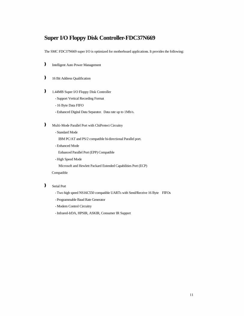
Super I/O Floppy Disk Controller-FDC37N669
The SMC FDC37N669 super I/O is optimized for motherboard applications. It provides the following:
� Intelligent Auto Power Management
� 16 Bit Address Qualification
� 1.44MB Super I/O Floppy Disk Controller
- Support Vertical Recording Format
- 16 Byte Data FIFO
- Enhanced Digital Data Separator. Data rate up to 1Mb/s.
� Multi-Mode Parallel Port with ChiProtect Circuitry
- Standard Mode
IBM PC/AT and PS/2 compatible bi-directional Parallel port.
- Enhanced Mode
Enhanced Parallel Port (EPP) Compatible
- High Speed Mode
Microsoft and Hewlett Packard Extended Capabilities Port (ECP)
Compatible
� Serial Port
- Two high speed NS16C550 compatible UARTs with Send/Receive 16 Byte FIFOs
- Programmable Baud Rate Generator
- Modem Control Circuitry
- Infrared-IrDA, HPSIR, ASKIR, Consumer IR Support
12
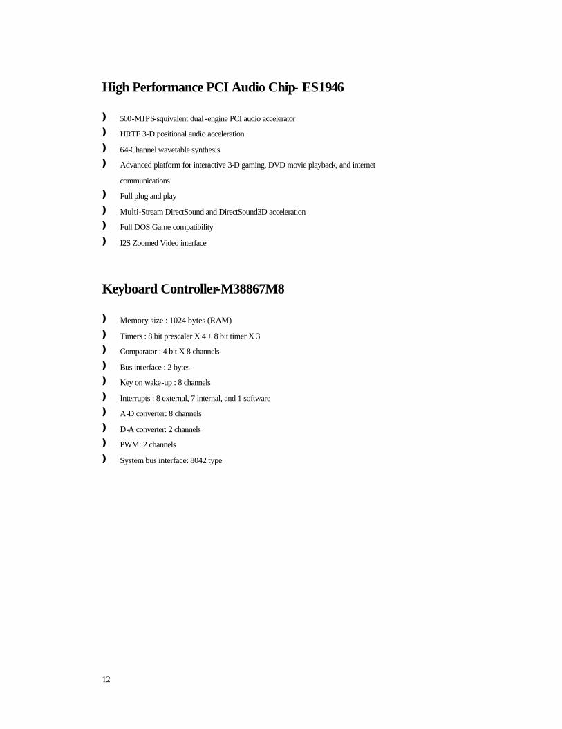
High Performance PCI Audio Chip- ES1946
� 500-MIPS-squivalent dual -engine PCI audio accelerator
� HRTF 3-D positional audio acceleration
� 64-Channel wavetable synthesis
� Advanced platform for interactive 3-D gaming, DVD movie playback, and internet
communications
� Full plug and play
� Multi-Stream DirectSound and DirectSound3D acceleration
� Full DOS Game compatibility
� I2S Zoomed Video interface
Keyboard Controller-M38867M8
� Memory size : 1024 bytes (RAM)
� Timers : 8 bit prescaler X 4 + 8 bit timer X 3
� Comparator : 4 bit X 8 channels
� Bus interface : 2 bytes
� Key on wake-up : 8 channels
� Interrupts : 8 external, 7 internal, and 1 software
� A-D converter: 8 channels
� D-A converter: 2 channels
� PWM: 2 channels
� System bus interface: 8042 type
13
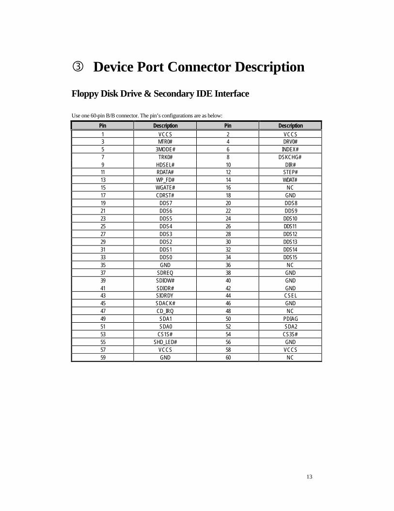
� Device Port Connector Description
Floppy Disk Drive & Secondary IDE Interface
Use one 60-pin B/B connector. The pin’s configurations are as below:
Pin Description Pin Description 1 VCCS 2 VCCS 3 MTR0# 4 DRV0# 5 3MODE# 6 INDEX# 7 TRK0# 8 DSKCHG# 9 HDSEL# 10 DIR# 11 RDATA# 12 STEP# 13 WP_FD# 14 WDAT# 15 WGATE# 16 NC 17 CDRST# 18 GND 19 DDS7 20 DDS8 21 DDS6 22 DDS9 23 DDS5 24 DDS10 25 DDS4 26 DDS11 27 DDS3 28 DDS12 29 DDS2 30 DDS13 31 DDS1 32 DDS14 33 DDS0 34 DDS15 35 GND 36 NC 37 SDREQ 38 GND 39 SDIOW# 40 GND 41 SDIOR# 42 GND 43 SIORDY 44 CSEL 45 SDACK# 46 GND 47 CD_IRQ 48 NC 49 SDA1 50 PDIAG 51 SDA0 52 SDA2 53 CS1S# 54 CS3S# 55 SHD_LED# 56 GND 57 VCCS 58 VCCS 59 GND 60 NC
14
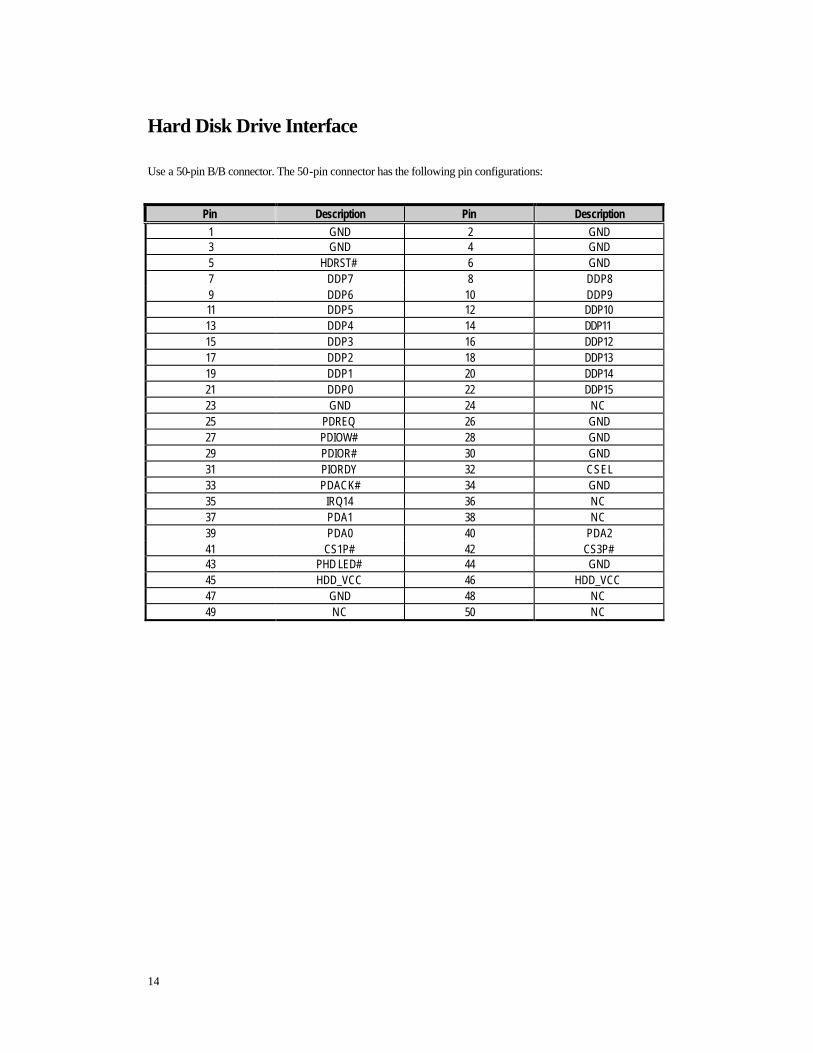
Hard Disk Drive Interface
Use a 50-pin B/B connector. The 50-pin connector has the following pin configurations:
Pin Description Pin Description 1 GND 2 GND 3 GND 4 GND 5 HDRST# 6 GND 7 DDP7 8 DDP8 9 DDP6 10 DDP9 11 DDP5 12 DDP10 13 DDP4 14 DDP11 15 DDP3 16 DDP12 17 DDP2 18 DDP13 19 DDP1 20 DDP14 21 DDP0 22 DDP15 23 GND 24 NC 25 PDREQ 26 GND 27 PDIOW# 28 GND 29 PDIOR# 30 GND 31 PIORDY 32 CSEL 33 PDACK# 34 GND 35 IRQ14 36 NC 37 PDA1 38 NC 39 PDA0 40 PDA2 41 CS1P# 42 CS3P# 43 PHD LED# 44 GND 45 HDD_VCC 46 HDD_VCC 47 GND 48 NC 49 NC 50 NC
15
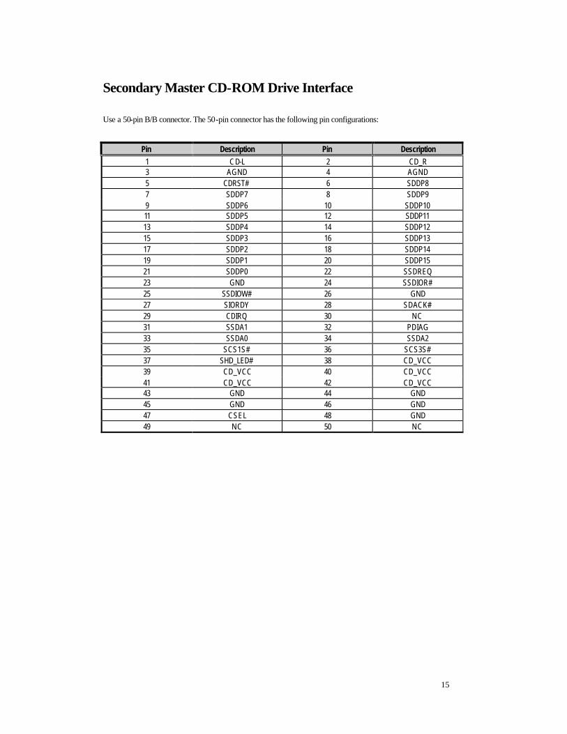
Secondary Master CD-ROM Drive Interface
Use a 50-pin B/B connector. The 50-pin connector has the following pin configurations:
Pin Description Pin Description 1 CD-L 2 CD_R 3 AGND 4 AGND 5 CDRST# 6 SDDP8 7 SDDP7 8 SDDP9 9 SDDP6 10 SDDP10 11 SDDP5 12 SDDP11 13 SDDP4 14 SDDP12 15 SDDP3 16 SDDP13 17 SDDP2 18 SDDP14 19 SDDP1 20 SDDP15 21 SDDP0 22 SSDREQ 23 GND 24 SSDIOR# 25 SSDIOW# 26 GND 27 SIORDY 28 SDACK# 29 CDIRQ 30 NC 31 SSDA1 32 PDIAG 33 SSDA0 34 SSDA2 35 SCS1S# 36 SCS3S# 37 SHD_LED# 38 CD_VCC 39 CD_VCC 40 CD_VCC 41 CD_VCC 42 CD_VCC 43 GND 44 GND 45 GND 46 GND 47 CSEL 48 GND 49 NC 50 NC
16
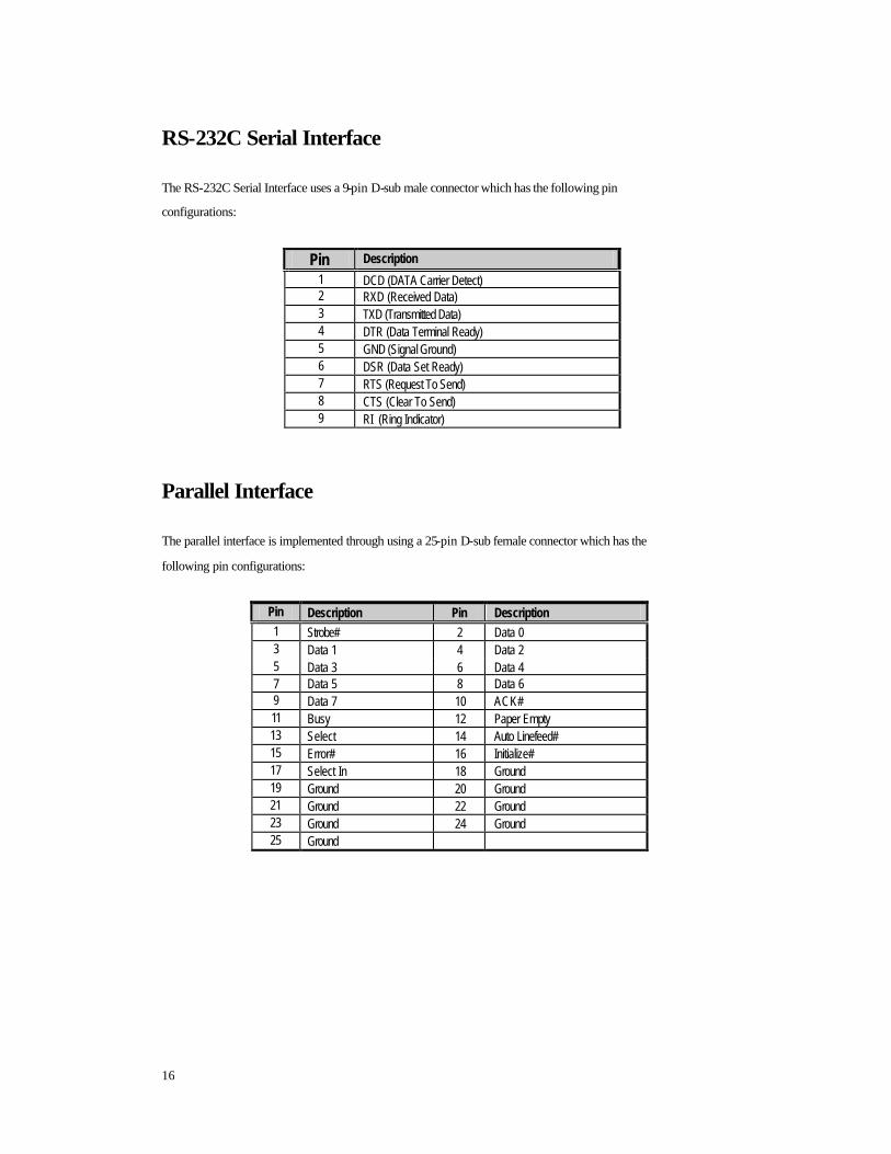
RS-232C Serial Interface
The RS-232C Serial Interface uses a 9-pin D-sub male connector which has the following pin
configurations:
Pin Description 1 DCD (DATA Carrier Detect) 2 RXD (Received Data) 3 TXD (Transmitted Data) 4 DTR (Data Terminal Ready) 5 GND (Signal Ground) 6 DSR (Data Set Ready) 7 RTS (Request To Send) 8 CTS (Clear To Send) 9 RI (Ring Indicator)
Parallel Interface
The parallel interface is implemented through using a 25-pin D-sub female connector which has the
following pin configurations:
Pin Description Pin Description 1 Strobe# 2 Data 0 3 Data 1 4 Data 2 5 Data 3 6 Data 4 7 Data 5 8 Data 6 9 Data 7 10 ACK# 11 Busy 12 Paper Empty 13 Select 14 Auto Linefeed# 15 Error# 16 Initialize# 17 Select In 18 Ground 19 Ground 20 Ground 21 Ground 22 Ground 23 Ground 24 Ground 25 Ground
17
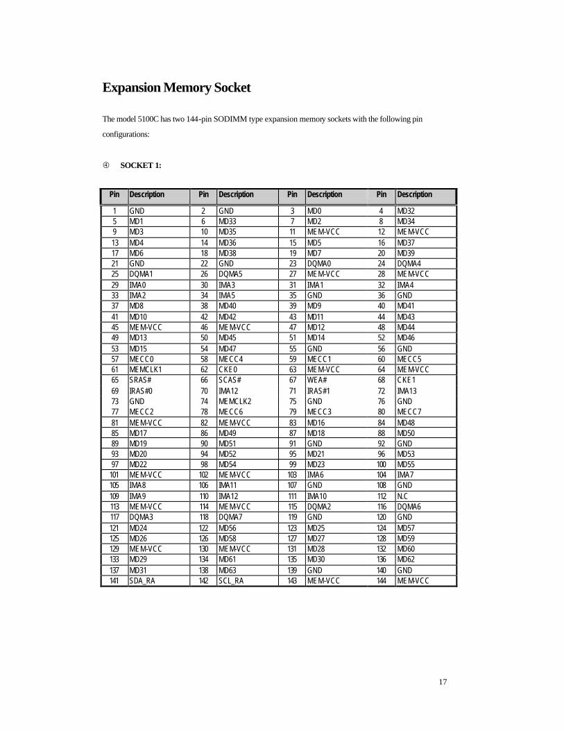
Expansion Memory Socket
The model 5100C has two 144-pin SODIMM type expansion memory sockets with the following pin
configurations:
� SOCKET 1:
Pin Description Pin Description Pin Description Pin Description
1 GND 2 GND 3 MD0 4 MD32 5 MD1 6 MD33 7 MD2 8 MD34 9 MD3 10 MD35 11 MEM-VCC 12 MEM-VCC 13 MD4 14 MD36 15 MD5 16 MD37 17 MD6 18 MD38 19 MD7 20 MD39 21 GND 22 GND 23 DQMA0 24 DQMA4 25 DQMA1 26 DQMA5 27 MEM-VCC 28 MEM-VCC 29 IMA0 30 IMA3 31 IMA1 32 IMA4 33 IMA2 34 IMA5 35 GND 36 GND 37 MD8 38 MD40 39 MD9 40 MD41 41 MD10 42 MD42 43 MD11 44 MD43 45 MEM-VCC 46 MEM-VCC 47 MD12 48 MD44 49 MD13 50 MD45 51 MD14 52 MD46 53 MD15 54 MD47 55 GND 56 GND 57 MECC0 58 MECC4 59 MECC1 60 MECC5 61 MEMCLK1 62 CKE0 63 MEM-VCC 64 MEM-VCC 65 SRAS# 66 SCAS# 67 WEA# 68 CKE1 69 IRAS#0 70 IMA12 71 IRAS#1 72 IMA13 73 GND 74 MEMCLK2 75 GND 76 GND 77 MECC2 78 MECC6 79 MECC3 80 MECC7 81 MEM-VCC 82 MEM-VCC 83 MD16 84 MD48 85 MD17 86 MD49 87 MD18 88 MD50 89 MD19 90 MD51 91 GND 92 GND 93 MD20 94 MD52 95 MD21 96 MD53 97 MD22 98 MD54 99 MD23 100 MD55
101 MEM-VCC 102 MEM-VCC 103 IMA6 104 IMA7 105 IMA8 106 IMA11 107 GND 108 GND 109 IMA9 110 IMA12 111 IMA10 112 N.C 113 MEM-VCC 114 MEM-VCC 115 DQMA2 116 DQMA6 117 DQMA3 118 DQMA7 119 GND 120 GND 121 MD24 122 MD56 123 MD25 124 MD57 125 MD26 126 MD58 127 MD27 128 MD59 129 MEM-VCC 130 MEM-VCC 131 MD28 132 MD60 133 MD29 134 MD61 135 MD30 136 MD62 137 MD31 138 MD63 139 GND 140 GND 141 SDA_RA 142 SCL_RA 143 MEM-VCC 144 MEM-VCC
18
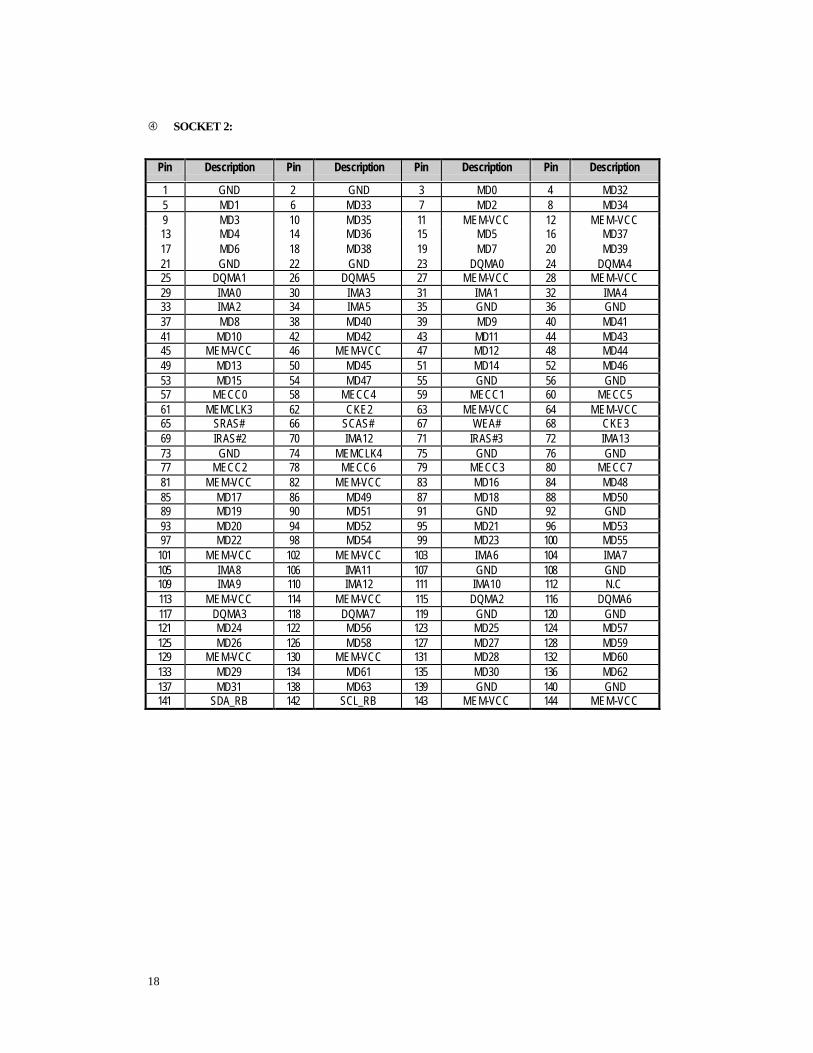
� SOCKET 2:
Pin Description Pin Description Pin Description Pin Description
1 GND 2 GND 3 MD0 4 MD32 5 MD1 6 MD33 7 MD2 8 MD34 9 MD3 10 MD35 11 MEM-VCC 12 MEM-VCC 13 MD4 14 MD36 15 MD5 16 MD37 17 MD6 18 MD38 19 MD7 20 MD39 21 GND 22 GND 23 DQMA0 24 DQMA4 25 DQMA1 26 DQMA5 27 MEM-VCC 28 MEM-VCC 29 IMA0 30 IMA3 31 IMA1 32 IMA4 33 IMA2 34 IMA5 35 GND 36 GND 37 MD8 38 MD40 39 MD9 40 MD41 41 MD10 42 MD42 43 MD11 44 MD43 45 MEM-VCC 46 MEM-VCC 47 MD12 48 MD44 49 MD13 50 MD45 51 MD14 52 MD46 53 MD15 54 MD47 55 GND 56 GND 57 MECC0 58 MECC4 59 MECC1 60 MECC5 61 MEMCLK3 62 CKE2 63 MEM-VCC 64 MEM-VCC 65 SRAS# 66 SCAS# 67 WEA# 68 CKE3 69 IRAS#2 70 IMA12 71 IRAS#3 72 IMA13 73 GND 74 MEMCLK4 75 GND 76 GND 77 MECC2 78 MECC6 79 MECC3 80 MECC7 81 MEM-VCC 82 MEM-VCC 83 MD16 84 MD48 85 MD17 86 MD49 87 MD18 88 MD50 89 MD19 90 MD51 91 GND 92 GND 93 MD20 94 MD52 95 MD21 96 MD53 97 MD22 98 MD54 99 MD23 100 MD55
101 MEM-VCC 102 MEM-VCC 103 IMA6 104 IMA7 105 IMA8 106 IMA11 107 GND 108 GND 109 IMA9 110 IMA12 111 IMA10 112 N.C 113 MEM-VCC 114 MEM-VCC 115 DQMA2 116 DQMA6 117 DQMA3 118 DQMA7 119 GND 120 GND 121 MD24 122 MD56 123 MD25 124 MD57 125 MD26 126 MD58 127 MD27 128 MD59 129 MEM-VCC 130 MEM-VCC 131 MD28 132 MD60 133 MD29 134 MD61 135 MD30 136 MD62 137 MD31 138 MD63 139 GND 140 GND 141 SDA_RB 142 SCL_RB 143 MEM-VCC 144 MEM-VCC
19
Internal trackpad Interface
The following is the pin configuration for the connector:
Pin Description 1 VCC 2 IMDATA 3 IMCLK 4 SWR 5 SWL 6 NC 7 NC 8 GND
External Monitor Interface
Use a 15-pin D-sub female connector that has the following configuration:
Pin Description 1 BRED 2 BGREEN 3 BBLUE 4 N.C 5 GND 6 GND 7 GND 8 GND 9 N.C 10 GND 11 N.C 12 DDCDA 13 DHSYNC 14 DVSYNC 15 DDCLK
RGB Out -
Output Impedance : 75�
RGB peak voltage: 0.7Vpp
External S-video TV-out Interface
Pin Description 1 GND 2 GND 3 LUMA 4 CRMA
20
External Keyboard/PS2 Mouse Interfac
Pin Description 1 EKDA 2 NC 3 GND 4 VCC 5 EKCLK 6 NC
External USB (Universal Serial Bus) Interface
Pin Description
1 USB_VCCA 2 USBP0- 3 USBP0+ 4 GND
21
PCMCIA CardBus Interface
� Socket A:
Pin Description Pin Description Pin Description
1 GND 35 GND 69 GND 2 A-CD3 36 A-CA5 70 A-CA19
3 A-CD4 37 A-CA4 71 A-CA20
4 GND 38 GND 72 GND 5 A-CD5 39 A-CA3 73 A-CA21
6 A-CD6 40 A-CA2 74 A-VCC-C
7 GND 41 GND 75 GND 8 A-CD7 42 A-CA1 76 GND
9 A-CE1# 43 A-CA0 77 A-VPP
10 GND 44 GND 78 A-CA22 11 A-CA10 45 A-CD0 79 GND
12 A-OE# 46 A-CD1 80 A-CA23
13 GND 47 GND 81 A-CA24 14 A-CA11 48 A-CD2 82 GND
15 A-CA9 49 A-WP# 83 A-CA25
16 GND 50 GND 84 A-VS2
17 A-CA8 51 GND 85 GND
18 A-CA13 52 A-CD1# 86 A-RESET
19 GND 53 A-CD11 87 A-WAIT# 20 A-CA14 54 GND 88 GND
21 A-WE# 55 A-CD12 89 A-INPACK
22 GND 56 A-CD13 90 A-REG#
23 A-RDYBY# 57 GND 91 GND
24 A-VCC-C 58 A-CD14 92 A-BVD2#
25 GND 59 A-CD15 93 A-BVD1#
26 GND 60 GND 94 GND 27 A-VPP 61 A-CE2# 95 A-CD8
28 A-CA16 62 A-VS1 96 A-CD9
29 GND 63 GND 97 GND 30 A-CA15 64 A-IORD# 98 A-CD10
31 A-CA12 65 A-IOWR# 99 A-CD2#
32 GND 66 GND 100 GND 33 A-CA7 67 A-CA17
34 A-CA6 68 A-CA18
22
� Socket B:
Pin Description Pin Description Pin Description
1 GND 35 GND 69 GND
2 B-CD3 36 B-CA5 70 B-CA19 3 B-CD4 37 B-CA4 71 B-CA20
4 GND 38 GND 72 GND
5 B-CD5 39 B-CA3 73 B-CA21 6 B-CD6 40 B-CA2 74 B-VCC-C
7 GND 41 GND 75 GND
8 B-CD7 42 B-CA1 76 GND
9 B-CE1# 43 B-CA0 77 B-VPP
10 GND 44 GND 78 B-CA22
11 B-CA10 45 B-CD0 79 GND
12 B-OE# 46 B-CD1 80 B-CA23 13 GND 47 GND 81 B-CA24
14 B-CA11 48 B-CD2 82 GND
15 B-CA9 49 B-WP# 83 B-CA25 16 GND 50 GND 84 B-VS2
17 B-CA8 51 GND 85 GND
18 B-CA13 52 B-CD1# 86 B-RESET 19 GND 53 B-CD11 87 B-WAIT#
20 B-CA14 54 GND 88 GND
21 B-WE# 55 B-CD12 89 B-INPACK 22 GND 56 B-CD13 90 B-REG#
23 B-RDYBY# 57 GND 91 GND
24 B-VCC-C 58 B-CD14 92 B-BVD2# 25 GND 59 B-CD15 93 B-BVD1#
26 GND 60 GND 94 GND
27 B-VPP 61 B-CE2# 95 B-CD8 28 B-CA16 62 B-VS1 96 B-CD9
29 GND 63 GND 97 GND
30 B-CA15 64 B-IORD# 88 B-CD10 31 B-CA12 65 B-IOWR# 99 B-CD2#
32 GND 66 GND 100 GND
33 B-CA7 67 B-CA17 34 B-CA6 68 B-CA18
23
LCD Interface ( For XGA TFT)
Pin Description Pin Description
1 LCDVDD 26 LCDVDD 2 GND 27 GND 3 PP0 28 PP2 4 PP1 29 PP3 5 GND 30 GND 6 PP4 31 PP6 7 PP5 32 PP7 8 GND 33 GND 9 PP12 34 PP10 10 PP13 35 PP11 11 GND 36 GND 12 PP16 37 PP14 13 PP17 38 PP15 14 GND 39 GND 15 VD48 40 VCC3 16 VD47 41 VCC3 17 GND 42 GND 18 INTMIC 43 MICGND 19 LID 44 BATON 20 ACIN 45 BAT_BEEP 21 BATCHA 46 BATFULL 22 ENABKKL 47 BRIGADJ 23 GND 48 GND 24 NC 49 NC 25 B+ 50 B+
24
PCI BUS Interface ( For Modem Option)
Pin (CON26)
Description Pin (CON26)
Description Pin (CON25)
Description
1 VCC3 35 AD11 1 AD23 2 VCC3 36 CBE#0 2 AD24
3 GND 37 AD10 3 AD22
4 GND 38 AD7 4 AD25
5 CBE#2 39 AD9 5 AD21 6 REQ#1 40 AD5 6 AD26
7 FRAME# 41 AD8 7 AD20
8 GNT#1 42 AD6 8 AD27 9 IRDY# 43 MONO_I 9 AD19
10 PCIMODEM 44 MONO_O 10 AD28
11 TRDY# 45 GND 11 AD18 12 PRST# 46 GND 12 AD29
13 DEVSEL# 47 GND 13 AD17
14 INT# 48 GND 14 AD30 15 STOP# 49 GND 15 AD16
16 TI_PME# 50 GND 16 AD31
17 PERR# 17 VCC
18 CRE#3 18 VCC
19 SERR# 19 VCC
20 IDSEL 20 VCC
21 VCC 21 VCC 22 VCC 22 VCC
23 PAR 23 GND
24 MODEMRI 24 GND 25 CBE#1 25 GND
26 AD4 26 GND
27 AD15 27 VCC3 28 AD3 28 VCC3
29 AD14 29 VCC3
30 AD2 30 VCC3 31 AD13
32 AD1
33 AD12 34 AD0
25
� DC/DC Converter Board
Input Characteristics
Input Voltage---From AC Adapter: 9.0V~21V
---From Battery: 12V
Efficiency
The total efficiency is 85% minimum at full load condition.
Output Characteristics
+5V and +3.45V Power on simultaneously
Voltage Regulation Ripple & Noise Current Typical Current Peak +5V �4% 150mVp-p 4.6A 6.4A
+3.45V �4% 150mVp-p 4.0A 6.0A +12V -5%~+5% 200mVp-p 0.2A 0.5A
System Alarm
Type Alarm Time Shut Down LI-ION (Dumb) 3-20 min 12.2V�0.5V NT-MH (Dumb) 3-20 min 7.6V�0.5V
26
� Inverter Board
Pin Assignment
� 12.1”(H) Connector 1; Input Connector
Pin No. Symbol Description 1 B+ Dc Voltage Supply the Operating Power 2 B+ Dc Voltage Supply the Operating Power 3 GND GND 4 GND GND 5 Brigadj Given an analog step by step signal in the rang of 0 to 2.5vdc to
Control the Lamp brightness 6 BKLO Control the Inverter ON/OFF
� 12.1”(V) Connector 1; Input Connector Pin No. Symbol Description
1 B+ Dc Voltage Supply the Operating Power 2 B+ Dc Voltage Supply the Operating Power 3 GND GND 4 GND GND 5 Brigadj Given an analog step by step signal in the rang of 0 to 2.5vdc to
Control the Lamp brightness 6 BKLO Control the Inverter ON/OFF
� Connector 2; Ouput Connector Pin No. Description
1 High voltage side of the Lamp 2 Low voltage side of the Lamp
Lamp Current: 2.5�0.5 ~ 5.0�0.5 Lamp Voltage: 600 Vrms Starting Voltage: 1400 @ 0� Working Frequency: 30~60 kHz Brightness Control: 0~2.5 Vdc B+: 7~22 V BKLO: 0V (OFF) 3.3V(ON)
27
� System Resource Allocation (In Windows 98)
IRQ:
IRQ 0: System timer
IRQ 1: Standard 101/102-key or Microsoft Natural Keyboard IRQ 2: Programmable interrupt controller
IRQ 3: Infrared PnP Serial Port (*PNP0510)
IRQ 4: CommunicationS Port (COM1) IRQ 5: ESS SOLO-1 PCI AudioDrive
IRQ 5: IRQ Holder for PCI Steering IRQ 6: Standard Floppy Disk Controller IRQ 7: Printer Port (LPT1) IRQ 8: System CMOS/real time clock
IRQ 9: Xircom CreditCard Ethernet Adapter 10/100 IRQ 10: Texas Instruments PCI-1225 CardBus Controller IRQ 10: Intel 8237/AB/EB PCI to USB Universial Host Controller
IRQ 10: IRQ Holder for PCI Steering IRQ 10: IRQ Holder for PCI Steering
IRQ 11: Texas Instruments PCI-1225 CardBus Controller
IRQ 11: IRQ Holder for PCI Steering IRQ 12: PS/2 Compatible Mouse Port
IRQ 13: Numeric data processor IRQ 14: Intel 8237/AB/EB PCI Bus Master IDE Controller IRQ 14: Primary IDE controller (dual fifo) IRQ 15: Intel 82371/AB/EB PCI Bus Master IDE Controller
IRQ 16: Secondary IDE controller (dual fifo)
DMA:
DMA 1: ESS SOLO-1 DOS Emulation
DMA 2: Standard Floppy Disk Controller
DMA 4: Direct memory access Controller
28
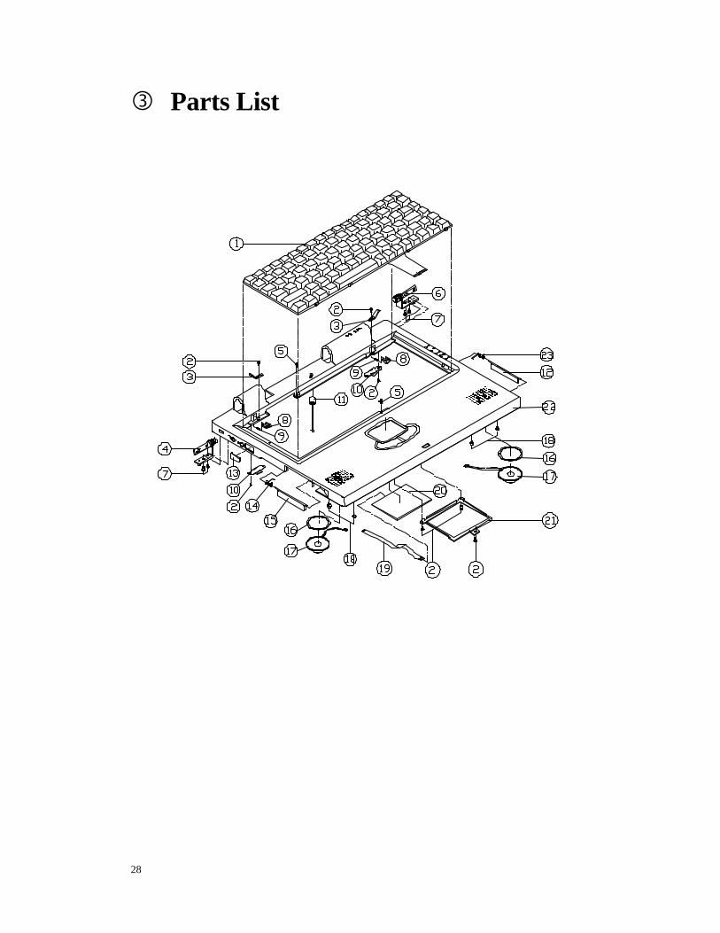
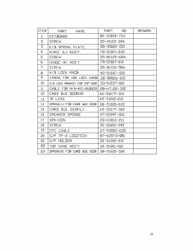
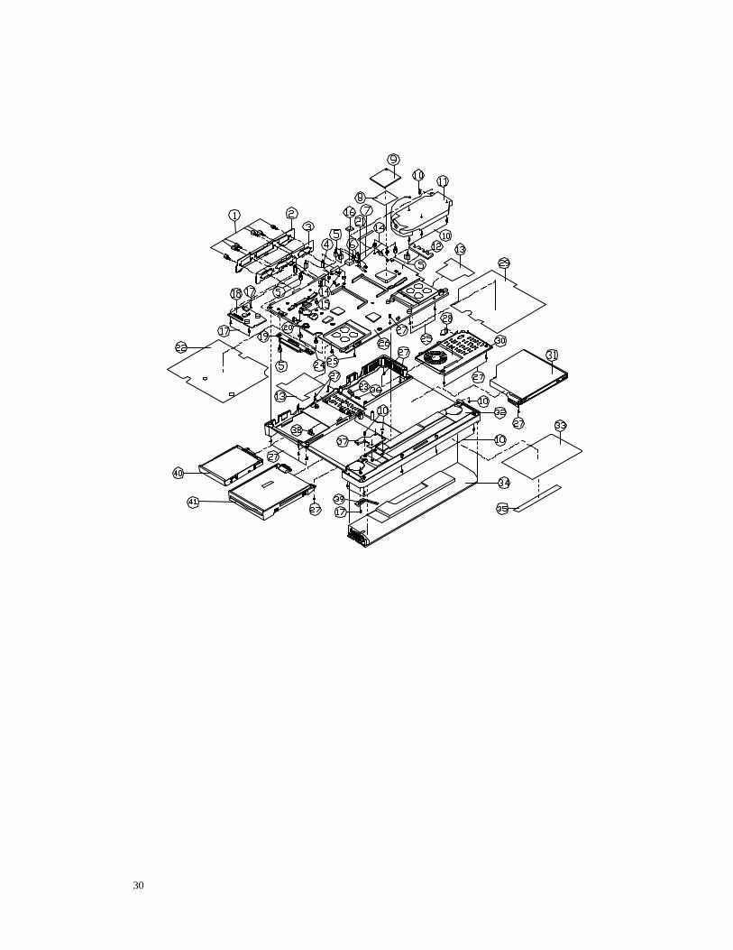
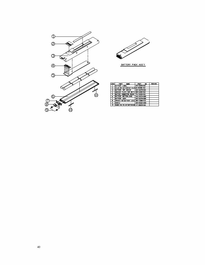
� Parts List
29
30

31
32
33
34
35
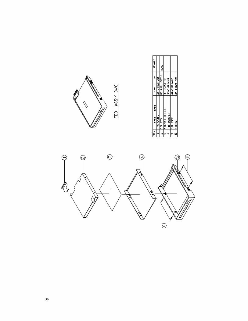
36
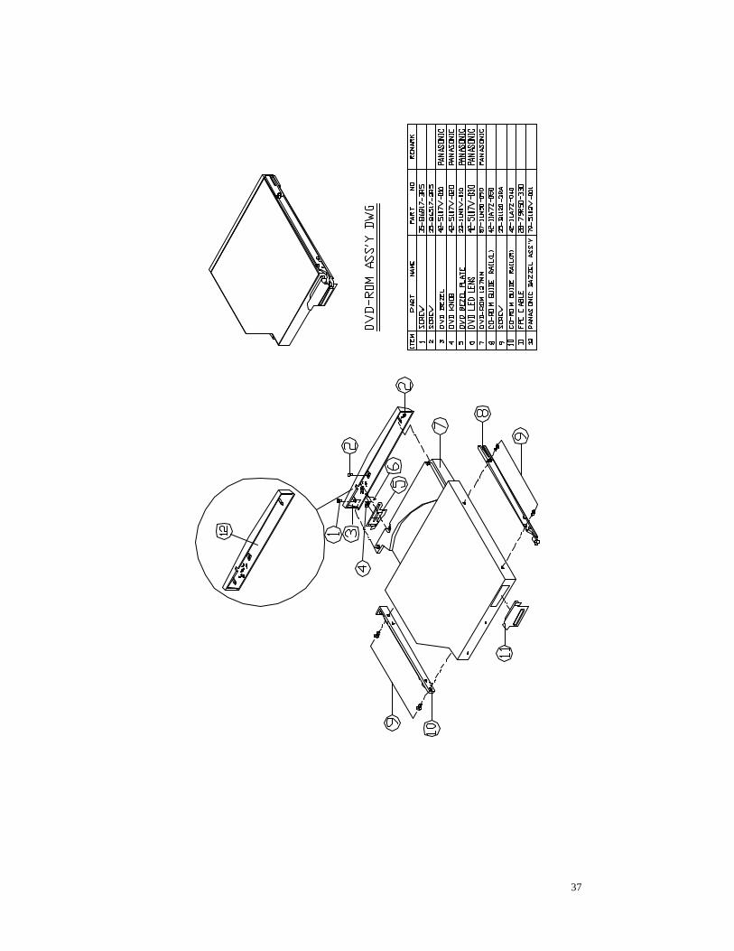
37
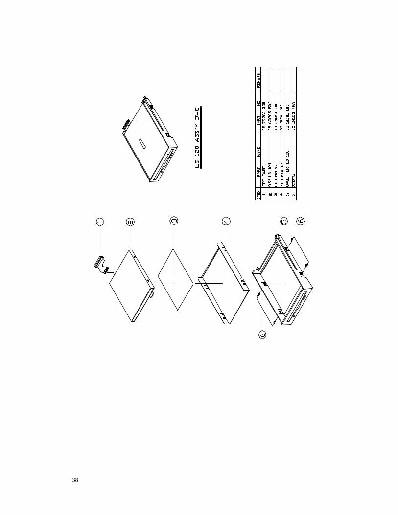
38
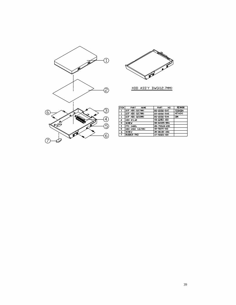
39
40
41
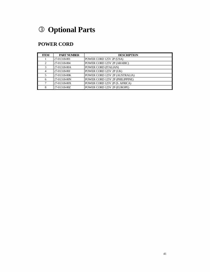
� Optional Parts
POWER CORD
ITEM PART NUMBER DESCRIPTION 1 27-01318-001 POWER CORD 125V 2P (USA) 2 27-01318-004 POWER CORD 125V 2P (ARABIC) 3 27-01318-00A POWER CORD (ITALIAN) 4 27-01318-00J POWER CORD 125V 2P (UK) 5 27-01318-00K POWER CORD 125V 2P (AUSTRALIA) 6 27-01318-00N POWER CORD 125V 2P (PHILIPPINE) 7 27-01318-00X POWER CORD 125V 2P (S. AFRICA) 8 27-01318-00Z POWER CORD 125V 2P (EUROPE)
42
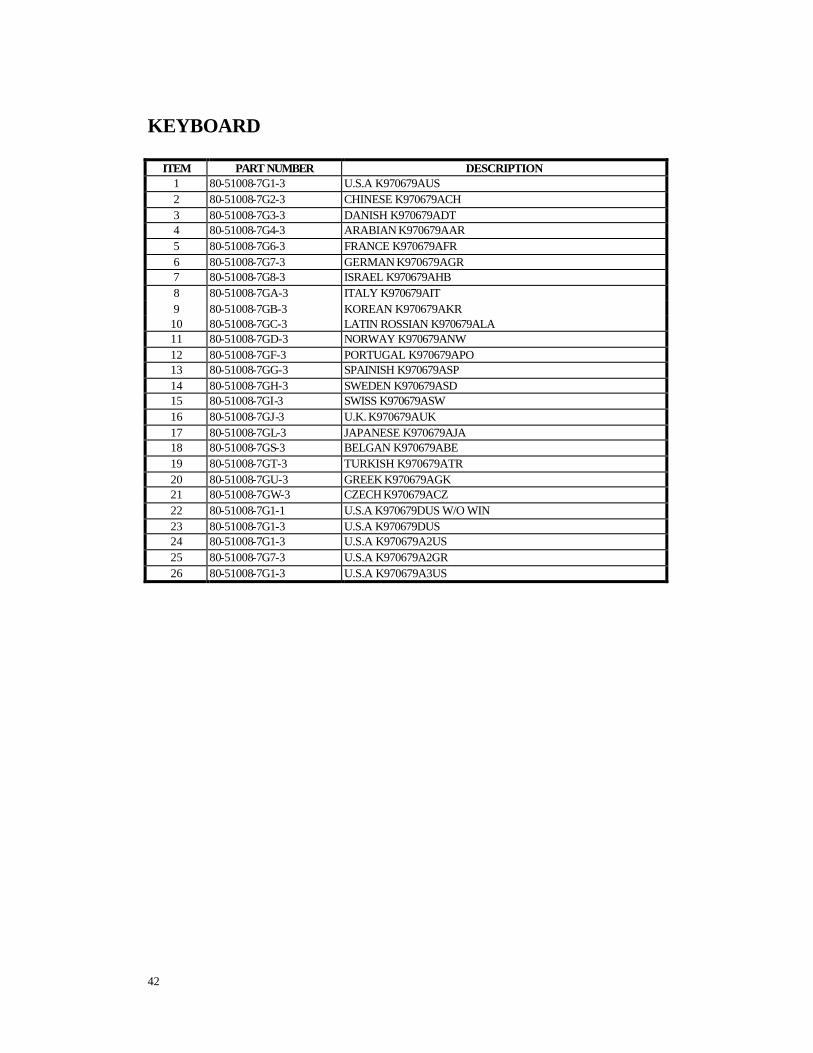
KEYBOARD
ITEM PART NUMBER DESCRIPTION 1 80-51008-7G1-3 U.S.A K970679AUS 2 80-51008-7G2-3 CHINESE K970679ACH 3 80-51008-7G3-3 DANISH K970679ADT 4 80-51008-7G4-3 ARABIAN K970679AAR 5 80-51008-7G6-3 FRANCE K970679AFR 6 80-51008-7G7-3 GERMAN K970679AGR 7 80-51008-7G8-3 ISRAEL K970679AHB 8 80-51008-7GA-3 ITALY K970679AIT 9 80-51008-7GB-3 KOREAN K970679AKR 10 80-51008-7GC-3 LATIN ROSSIAN K970679ALA 11 80-51008-7GD-3 NORWAY K970679ANW 12 80-51008-7GF-3 PORTUGAL K970679APO 13 80-51008-7GG-3 SPAINISH K970679ASP 14 80-51008-7GH-3 SWEDEN K970679ASD 15 80-51008-7GI-3 SWISS K970679ASW 16 80-51008-7GJ-3 U.K. K970679AUK 17 80-51008-7GL-3 JAPANESE K970679AJA 18 80-51008-7GS-3 BELGAN K970679ABE 19 80-51008-7GT-3 TURKISH K970679ATR 20 80-51008-7GU-3 GREEK K970679AGK 21 80-51008-7GW-3 CZECH K970679ACZ 22 80-51008-7G1-1 U.S.A K970679DUS W/O WIN 23 80-51008-7G1-3 U.S.A K970679DUS 24 80-51008-7G1-3 U.S.A K970679A2US 25 80-51008-7G7-3 U.S.A K970679A2GR 26 80-51008-7G1-3 U.S.A K970679A3US

![Wireless Starter Kit Mainboard - Silicon Labs · vcom_enable pti0[0..2] vmcu gnd gnd gnd gnd vmcu vrf 5v 3v3 gnd vrf gnd gnd gnd gnd gnd usb_vbus usb_vreg usb_vbus 5v 5v_dbg …](https://img.pdfslide.us/doc/110x75/5ac0fbea7f8b9a4e7c8c7c14/wireless-starter-kit-mainboard-silicon-labs-pti002-vmcu-gnd-gnd-gnd-gnd-vmcu.jpg)