Embed Size (px)
Citation preview

MOCVD growth system

General MOCVD growth features
• Advantages– Faster growth than MBE, can be a few microns per
hour; multi-wafer capability easily achievable– Higher temperature growth; growth process is
thermodynamically favorable– Quality of layers usually better than MBE
• Disadvantages– Difficult to monitor growth rate exactly (no Rheed
possible due to higher pressure)– Not as abrupt a process as MBE due to gas flow
issues and memory effects– Toxic gases are to be handled
MOCVD growth of III-nitrides
• Precursors for III: TMGa, TMAl, TMIn; for V: NH3, Hydrogen carrier gas; 25-760 Torr pressure
• Growth of GaN is carried out at 1000 – 1100 °C, which is much higher than the MBE growth temperature
• Growth on both SiC and sapphire substrates have been optimized and used regularly
• If SiC is used as substrate, it can be etched in-situ to get very smooth surface showing step flow
• Growth always results in Ga-face polarity irrespective of the nucleation layer used
• Problem of hydrogen passivation of p-type dopants, since hydrogen is used as the carrier gas
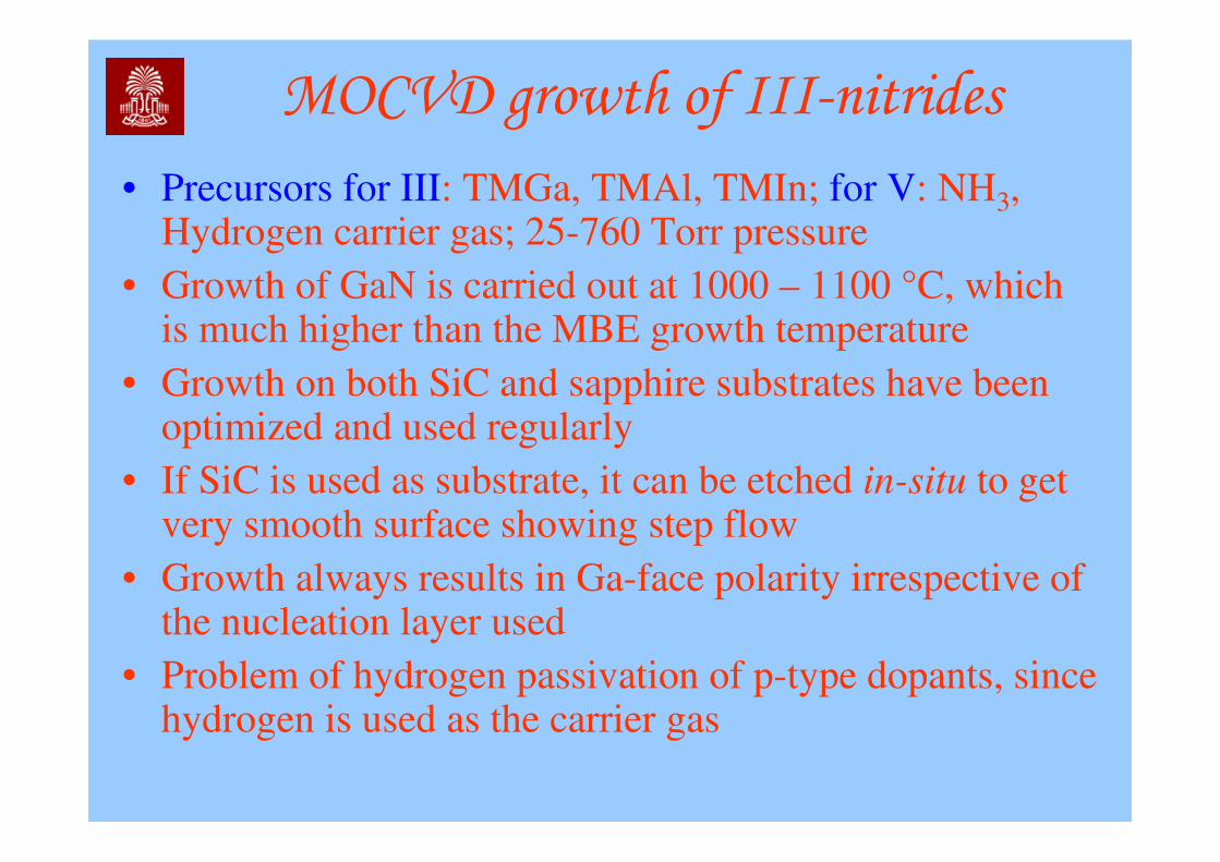
Basics of MOCVD growth of Nitrides
• Important growth parameters: growth temperature T and V/III ratio
• T too high: desorption, nitrogen vacancies. T too low: impurities incorporation, low surface mobility, structure defects; Usually temperature ~1050 °C
• V/III ratio too high: III-atoms low surface mobility, structure defects. Too low:decompose, nitrogen vacancies, auto background doping
Gro
wth
rat
e
Best growth zone
Kineti
cs-li
mited
Thermodynam
ics-limited
Temperature
Diffusion controlled
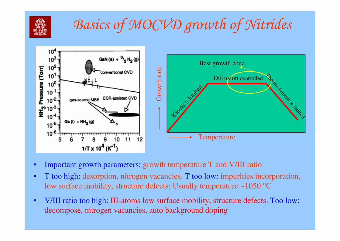
MOCVD growth of Nitrides on sapphire
• A two-step growth method is followed with the growth of a low temperature AlN layer
• Before any growth, the sapphire surface is nitridated to reduce defect density by causing changes in surface energy
• The low temperature layer can be either GaN, AlN or even AlGaN
• In MOCVD growth (unlike growth by MBE), the polarity of the GaN film is always Ga-face
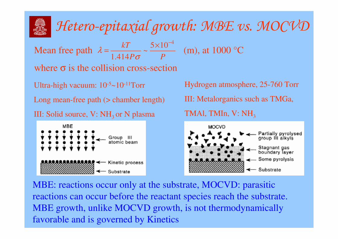
Hetero-epitaxial growth: MBE vs. MOCVD
MBE: reactions occur only at the substrate, MOCVD: parasitic reactions can occur before the reactant species reach the substrate. MBE growth, unlike MOCVD growth, is not thermodynamically favorable and is governed by Kinetics
Mean free path (m), at 1000 °C PP
kT4105
~414.1
−×=
σλ
Ultra-high vacuum: 10-5~10-11Torr
Long mean-free path (> chamber length)
III: Solid source, V: NH3 or N plasma
Hydrogen atmosphere, 25-760 Torr
III: Metalorganics such as TMGa,
TMAl, TMIn, V: NH3
where σ is the collision cross-section
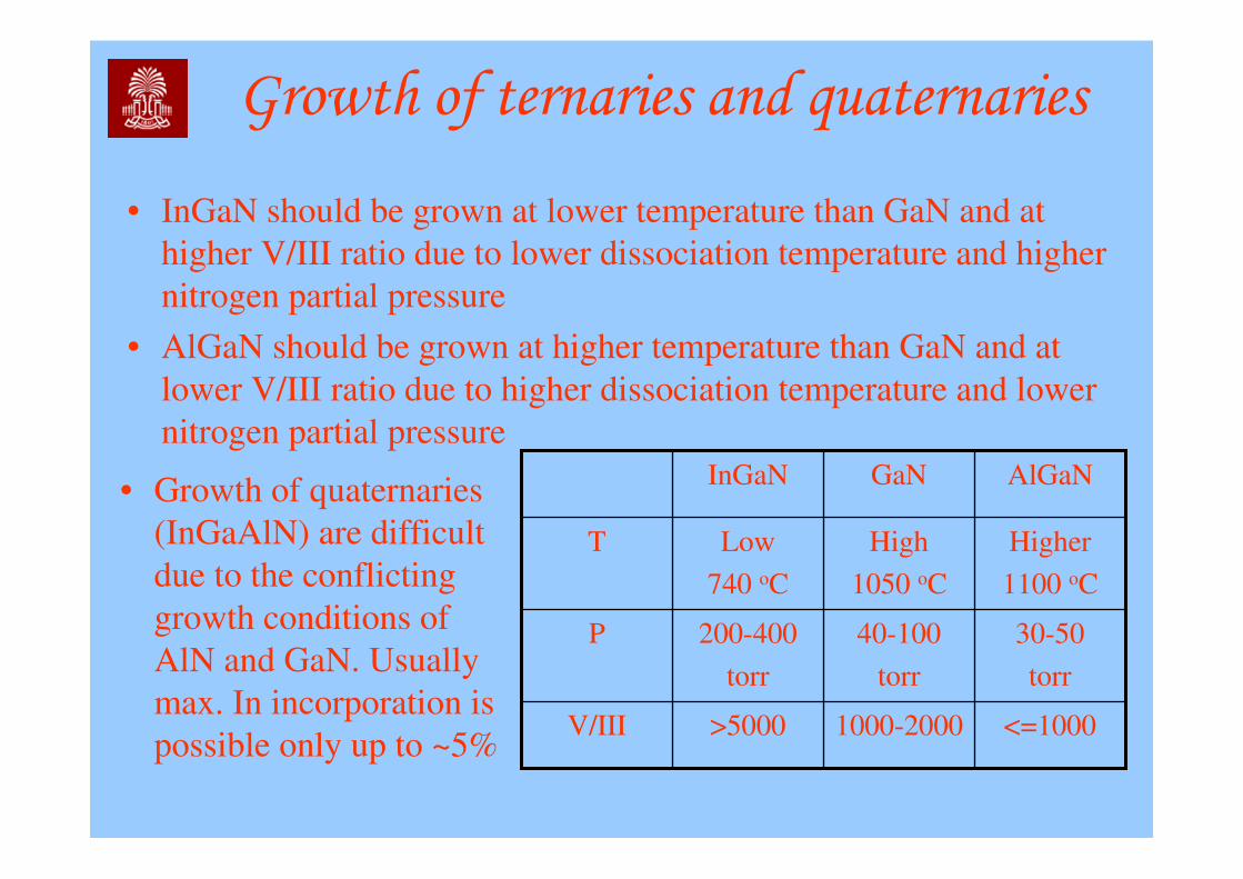
Growth of ternaries and quaternaries
• InGaN should be grown at lower temperature than GaN and at higher V/III ratio due to lower dissociation temperature and higher nitrogen partial pressure
• AlGaN should be grown at higher temperature than GaN and at lower V/III ratio due to higher dissociation temperature and lower nitrogen partial pressure
<=10001000-2000>5000V/III
30-50
torr
40-100
torr
200-400
torr
P
Higher
1100 oC
High
1050 oC
Low
740 oC
T
AlGaNGaNInGaN• Growth of quaternaries (InGaAlN) are difficult due to the conflicting growth conditions of AlN and GaN. Usually max. In incorporation is possible only up to ~5%
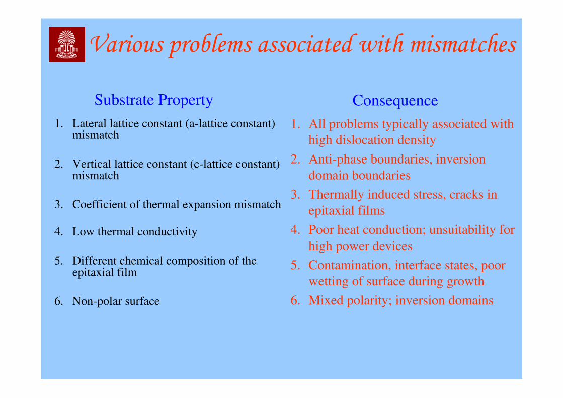
Various problems associated with mismatches
1. Lateral lattice constant (a-lattice constant) mismatch
2. Vertical lattice constant (c-lattice constant) mismatch
3. Coefficient of thermal expansion mismatch
4. Low thermal conductivity
5. Different chemical composition of the epitaxial film
6. Non-polar surface
Substrate Property Consequence1. All problems typically associated with
high dislocation density
2. Anti-phase boundaries, inversion domain boundaries
3. Thermally induced stress, cracks in epitaxial films
4. Poor heat conduction; unsuitability for high power devices
5. Contamination, interface states, poor wetting of surface during growth
6. Mixed polarity; inversion domains
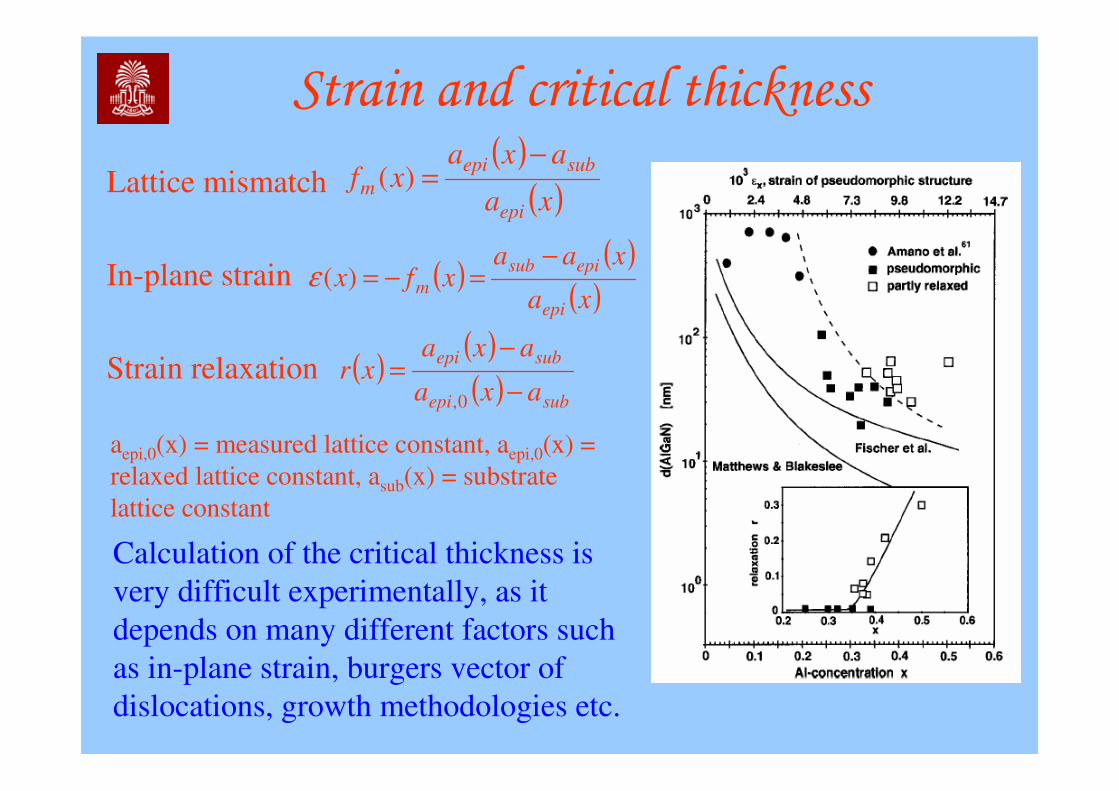
Strain and critical thickness
Lattice mismatch( )
( )xa
axaxf
epi
subepi
m
−=)(
In-plane strain ( )( )
( )xa
xaaxfx
epi
episub
m
−=−=)(ε
( )( )( ) subepi
subepi
axa
axaxr
−
−=
0,
Strain relaxation
aepi,0(x) = measured lattice constant, aepi,0(x) = relaxed lattice constant, asub(x) = substrate lattice constant
Calculation of the critical thickness is very difficult experimentally, as it depends on many different factors such as in-plane strain, burgers vector of dislocations, growth methodologies etc.
Formation of dislocations
• Dislocations are formed in the epitaxial layers due to– Transfer of defects/dislocations already present in the substrate:
Happens when substrate has high density of defects (example: dislocation in GaN epilayers when SiC is used as a substrate)
– Misfit dislocation: When dislocations are caused by a difference in the lattice constant of the epitaxial layer and the substrate (Ex: dislocations in AlGaN layer (dAlGaN > dcritical) grown on GaN)
– Imperfections resulting from island coalescence (example: dislocations in GaN buffer layers grown on AlN nucleation layer)
• Main types of defects in GaN– Point defects (vacancies, self-interstitials, and antisites)– Threading edge dislocation– Threading screw dislocation– Mixed screw-edge dislocations
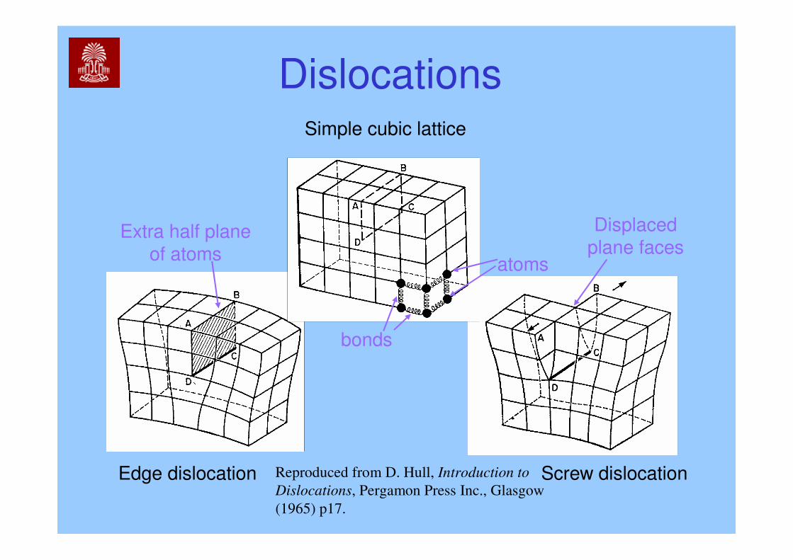
Dislocations
Reproduced from D. Hull, Introduction to
Dislocations, Pergamon Press Inc., Glasgow (1965) p17.
Simple cubic lattice
atoms
bonds
Edge dislocation
Extra half plane of atoms
Screw dislocation
Displaced plane faces
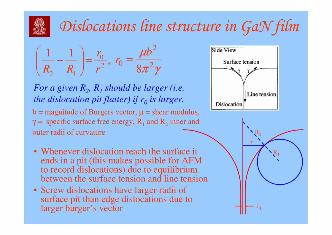
Dislocations line structure in GaN film
• Whenever dislocation reach the surface it ends in a pit (this makes possible for AFM to record dislocations) due to equilibrium between the surface tension and line tension
• Screw dislocations have larger radii of surface pit than edge dislocations due to larger burger’s vector
r
R2
R1
r0
,11
20
12 r
r
RR=
−
γπ
µ2
2
08
br =
b = magnitude of Burgers vector, µ = shear modulus, γ = specific surface free energy, R1 and R2 inner and outer radii of curvature
For a given R2, R1 should be larger (i.e.
the dislocation pit flatter) if r0 is larger.
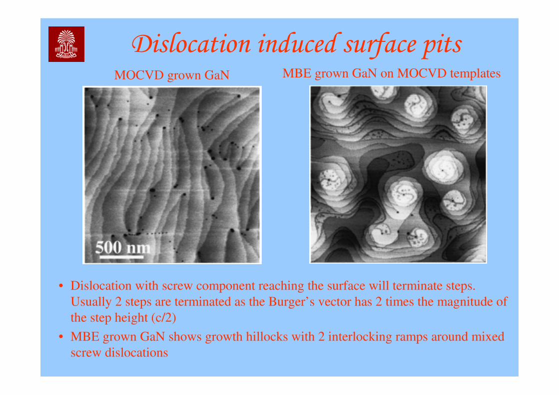
Dislocation induced surface pits
• Dislocation with screw component reaching the surface will terminate steps. Usually 2 steps are terminated as the Burger’s vector has 2 times the magnitude of the step height (c/2)
• MBE grown GaN shows growth hillocks with 2 interlocking ramps around mixed screw dislocations
MOCVD grown GaN MBE grown GaN on MOCVD templates
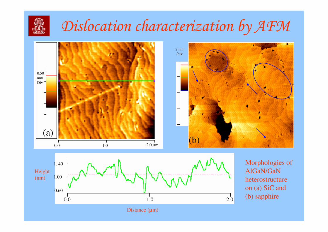
Dislocation characterization by AFM2 nm/div
(b)0.0 1.0 2.0 µm
0.50 nm/Div
Distance (µm)
Height (nm)
0.0 1.0 2.0
0.60
1.00
1. 40
(a)
Morphologies of AlGaN/GaNheterostructureon (a) SiC and (b) sapphire
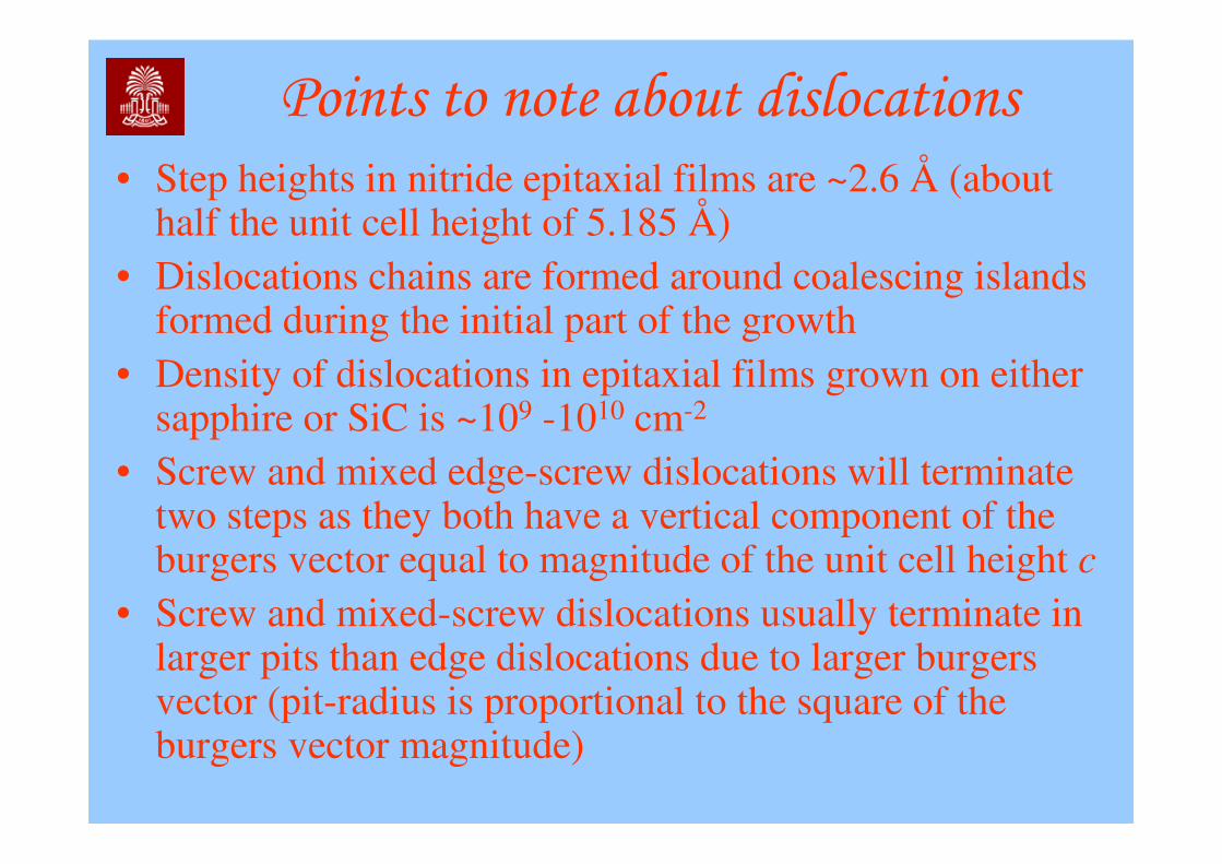
Points to note about dislocations
• Step heights in nitride epitaxial films are ~2.6 Å (about half the unit cell height of 5.185 Å)
• Dislocations chains are formed around coalescing islands formed during the initial part of the growth
• Density of dislocations in epitaxial films grown on either sapphire or SiC is ~109 -1010 cm-2
• Screw and mixed edge-screw dislocations will terminate two steps as they both have a vertical component of the burgers vector equal to magnitude of the unit cell height c
• Screw and mixed-screw dislocations usually terminate in larger pits than edge dislocations due to larger burgers vector (pit-radius is proportional to the square of the burgers vector magnitude)
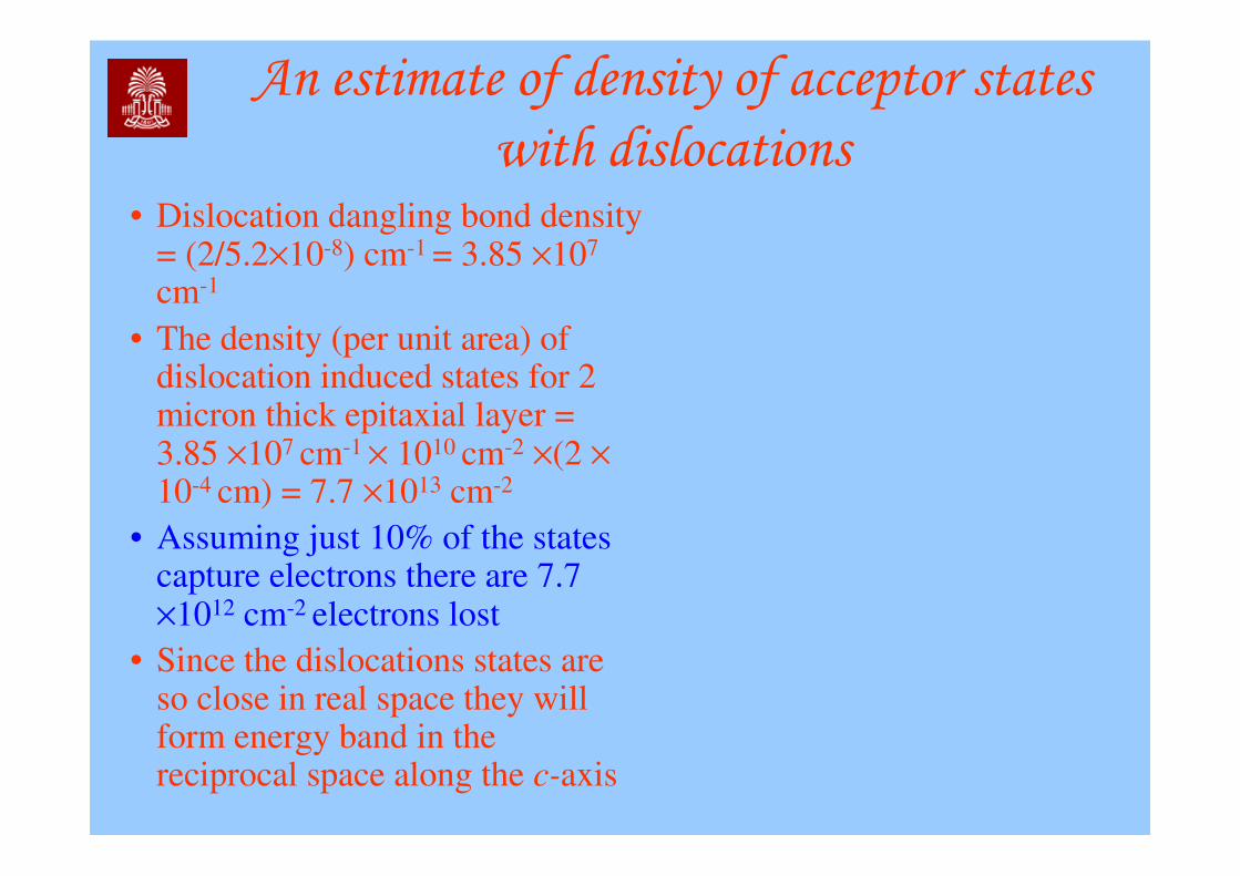
An estimate of density of acceptor states
with dislocations• Dislocation dangling bond density
= (2/5.2×10-8) cm-1 = 3.85 ×10⁷
cm-1
• The density (per unit area) of dislocation induced states for 2 micron thick epitaxial layer = 3.85 ×107 cm-1 × 1010 cm-2 ×(2 ×10-4 cm) = 7.7 ×1013 cm-2
• Assuming just 10% of the states capture electrons there are 7.7 ×1012 cm-2 electrons lost
• Since the dislocations states are so close in real space they will form energy band in the reciprocal space along the c-axis
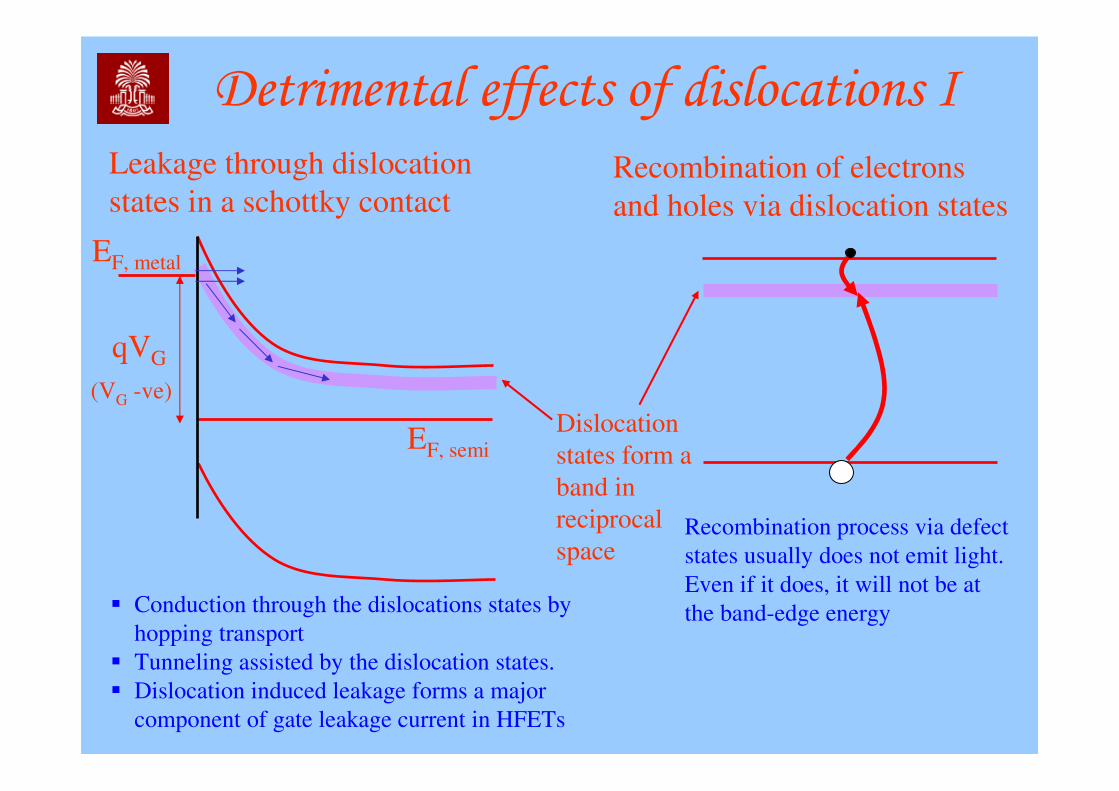
Detrimental effects of dislocations I
� Conduction through the dislocations states by hopping transport
� Tunneling assisted by the dislocation states.� Dislocation induced leakage forms a major
component of gate leakage current in HFETs
EF, metal
EF, semi
qVG
(VG -ve)Dislocation states form a band in reciprocal space
Recombination process via defect states usually does not emit light. Even if it does, it will not be at the band-edge energy
Leakage through dislocation states in a schottky contact
Recombination of electrons and holes via dislocation states