Embed Size (px)
Citation preview
Moby-Dic Workshop, Noordwijkerhout, August 23, 2012
ASIC Implementation of the ASIC Implementation of the PWA Generic Canonical FormPWA Generic Canonical Form
Dpto. Electrónica y Electromagnetismo, Universidad de Sevilla
Instituto de Microelectrónica de Sevilla-CNM-CSIC; [email protected]
MOBY-DIC Project FP7-IST-248858Noordwijkerhout, August 23, 2012
Antonio J. Acosta

Moby-Dic Workshop, Noordwijkerhout, August 23, 2012
Introduction: Role of ASICs in control & characteristics of
ASICs
Design of MPC_ASICs: From high-level specifications to
silicon
PWAG Architecture Selection
Design, Integration and test of a PWAG ASIC
Test Results
Outline of the presentationOutline of the presentation
Moby-Dic Workshop, Noordwijkerhout, August 23, 2012
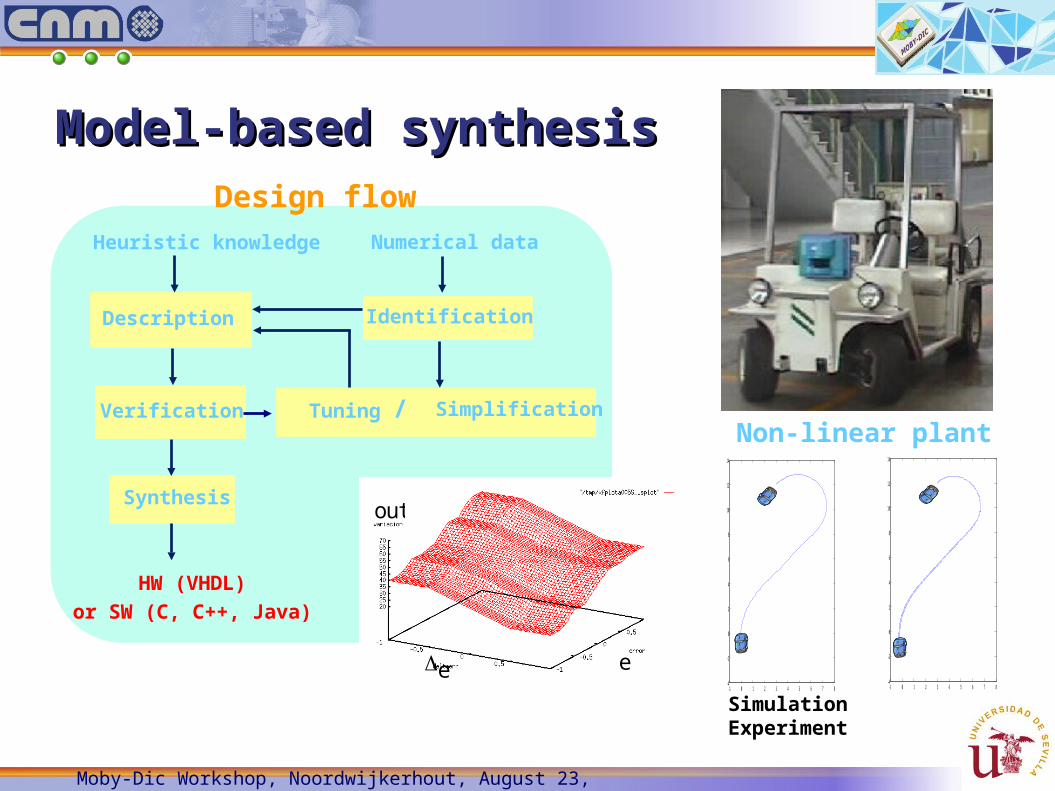
Model-based synthesisModel-based synthesis
Description
Design flow
Simplification
Heuristic knowledge Numerical data
Verification
Synthesis
Tuning /
Identification
HW (VHDL)or SW (C, C++, Java)
Non-linear plant
-1 0 1 2 3 4 5 6 7 8-4
-2
0
2
4
6
8
10
12
14
-1 0 1 2 3 4 5 6 7 8-4
-2
0
2
4
6
8
10
12
14
-1 0 1 2 3 4 5 6 7 8-4
-2
0
2
4
6
8
10
12
14
-1 0 1 2 3 4 5 6 7 8-4
-2
0
2
4
6
8
10
12
14
Simulation Experiment
ee
out

Moby-Dic Workshop, Noordwijkerhout, August 23, 2012
Dedicated HW
Digital ASIC
Embedded ControllerEmbedded Controller
Externalmemories
Testboard
FPGAExpansion boards
DSP FPGA
Embedded SW
- Performances ++ Flexibility -
- Cost +

Moby-Dic Workshop, Noordwijkerhout, August 23, 2012
ASIC Design Process
FINAL
CONCEPTIONAND
SPECIFICATIONS
DESIGNAND
VALIDATION
ASIC FABRICATION
Final designtape-out
- Viability analysis
- Alternatives vs. constraints
- Cost analysis:
- Added values:
IPs Libraries
Low-cost solutions (FPGAs)
EUROPRACTICE: Interface with CAD vendors & foundries
DESIGN HOUSE
CLIENT
FOUNDRY (TSMC)
- Flexibility in specifications
+ Development: human, technical, ...+ Production: Silicon
+ Testing, reliability, ...
Test of final ASICTech Info:Devices modeling
ASIC
Cell libraries
CADVENDORS
EDA toolssupport
TESTHOUSE
TestersDfT
+ Time-to-market, 1st silicon success, ...
Moby-Dic Workshop, Noordwijkerhout, August 23, 2012
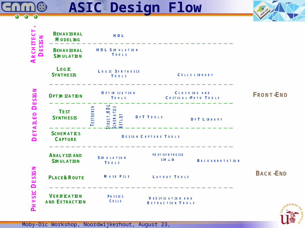
FRONT-END
BACK-END
H DL
H DL S IM U L A T IO N
T O O L S
L O G IC S Y N T H E S I S
T O O L S
O P T IM I Z A T I O N
TO O L S
C E L L S L IB R A R Y
C L O C K I N G A N D
C R I T I C A L -P A T H TO O L S
D F T T O O L SD F T L IB R A R Y
D E S I G N C A P T U R E T O O L S
S TRU
CT.
HD
L
NET
LIST
S CH
EMA
TICS
T EST
BENC
H
S IM U L A T I O N
TO O L S
L A Y O U T TO O L S
PO ST-SY N THE SIS
V E R I F IC A T IO N A N D
M A S K F I L E
SIM.L IB B A C K A N N O T A T IO N
PH YS IC S
CE LLS E X T R A C T I O N T O O L S
DE
SIG
ND
ET
AIL
ED
DE
SIG
NP
HY
SIC
DE
SIG
NA
RC
HIT
EC
T.
BEHAVIORALMODELING
BEHAVIORALSIMULATION
LOGICSYNTHESIS
OPTIMIZATION
TEST
SYNTHESIS
SCHEMATICSCAPTURE
ANALYSIS ANDSIMULATION
PLACE&ROUTE
VERIFICATIONAND EXTRACTION
ASIC Design Flow
Moby-Dic Workshop, Noordwijkerhout, August 23, 2012
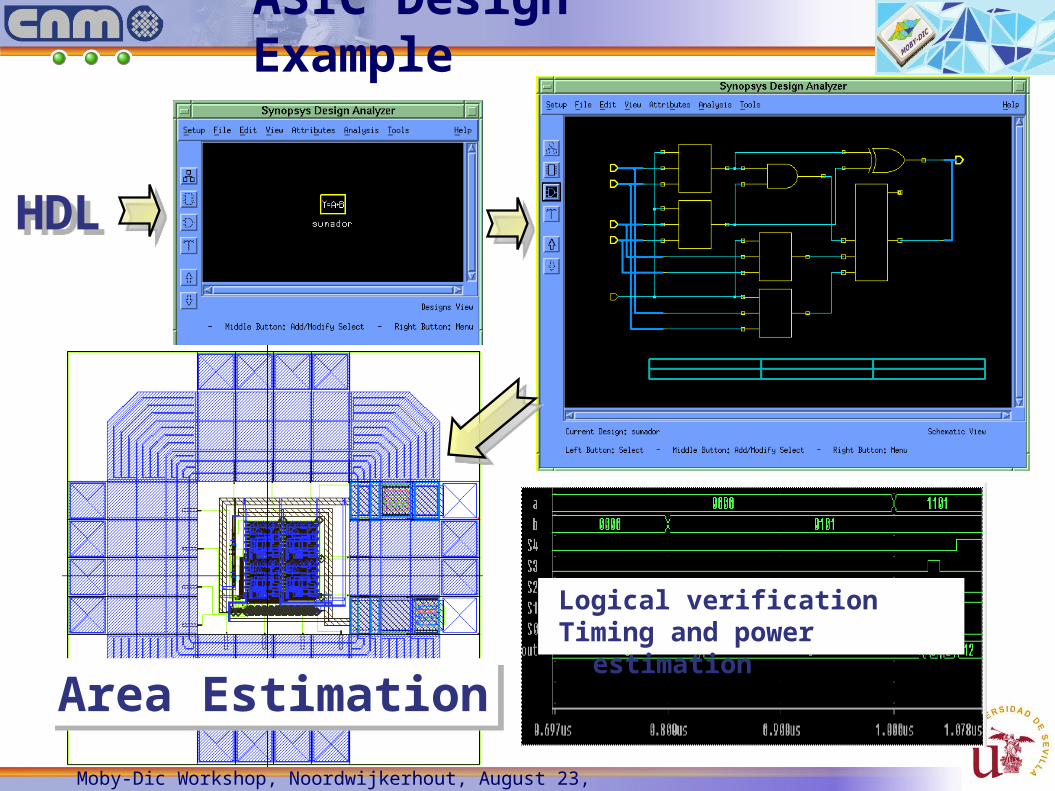
ASIC Design Example
HDLHDL
Area EstimationArea Estimation
Logical verification Timing and power
estimation
Moby-Dic Workshop, Noordwijkerhout, August 23, 2012
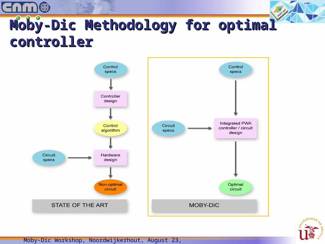
Moby-Dic Methodology for optimal controllerMoby-Dic Methodology for optimal controller

Moby-Dic Workshop, Noordwijkerhout, August 23, 2012
Control and Circuit decisions
Canonical form (PWAG)
No. input-output
Precision
Control surface
…
Configurable architecture
Parametrizable design
Programmability issues
HW requirements & limitations
…MOBY-DICTOOLBOX
HDL code ParametersFOR SELECTED CASE-STUDIES

Moby-Dic Workshop, Noordwijkerhout, August 23, 2012
Proposed PWAG ArchitectureProposed PWAG Architecture
MEMORY
FSM
Modification of the one in [OLIV09]
The binary tree is stored in a Memory
The data in the TreeMemory are the address of ParamMemory
Less rigid, more configurable (different trees, on-line computation)
Moby-Dic Workshop, Noordwijkerhout, August 23, 2012
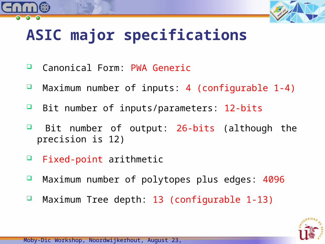
Canonical Form: PWA Generic
Maximum number of inputs: 4 (configurable 1-4)
Bit number of inputs/parameters: 12-bits
Bit number of output: 26-bits (although the precision is 12)
Fixed-point arithmetic
Maximum number of polytopes plus edges: 4096
Maximum Tree depth: 13 (configurable 1-13)
ASIC major specifications

Moby-Dic Workshop, Noordwijkerhout, August 23, 2012
Technology and CAD Tools SelectionTaiwan Semiconductor Manufacturing Company (TSMC)
90 nm, 9 metal layers
MiniAsic:1,875 x 1,875 µm2 (2011), 100 samples.
Memories on Chip
Dual Port RAM Memories
Access and Writing times below 5 ns (worst case)
CAD tools used:
DESIGN ANALYZER (SYNOPSYS)
SOC ENCOUNTER, DFWII (CADENCE)
Moby-Dic Workshop, Noordwijkerhout, August 23, 2012
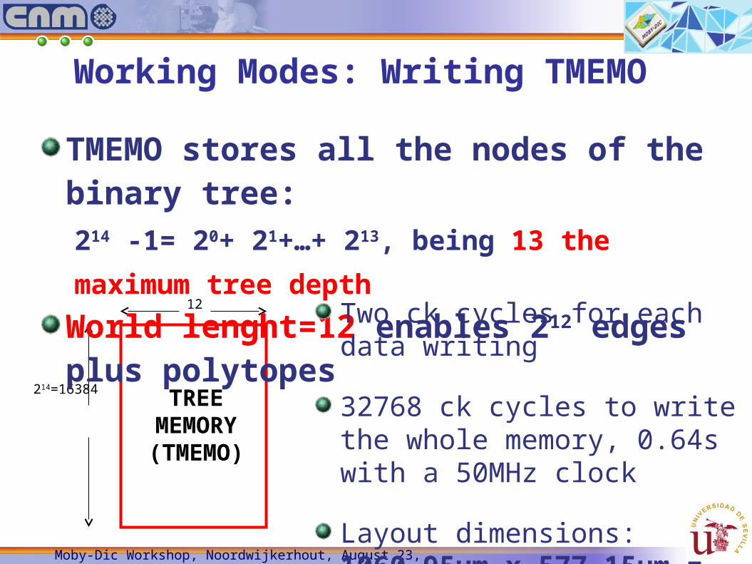
214=16384 TREE MEMORY (TMEMO)
12
TMEMO stores all the nodes of the binary tree:214 -1= 20+ 21+…+ 213, being 13 the maximum tree depth
World lenght=12 enables 212 edges plus polytopes
Two ck cycles for each data writing
32768 ck cycles to write the whole memory, 0.64s with a 50MHz clock
Layout dimensions: 1060.95µm x 577.15µm = 612332.6µm2
Working Modes: Writing TMEMO

Moby-Dic Workshop, Noordwijkerhout, August 23, 2012
212=4096 PARAMETER MEMORY (PMEMO)
60
PMEMO stores all the possible edges and polytopes212 = 4096 edges plus polytopes
World lenght=60 enables 5 12-bit parametersSix ck cycles for each data writing
24576 ck cycles to write the whole memory, 0.48s with a 50MHz clock
Layout dimensions: 1190.51µm x 569.12µm = 677543.1µm2
Working Modes: Writing PMEMO
Moby-Dic Workshop, Noordwijkerhout, August 23, 2012
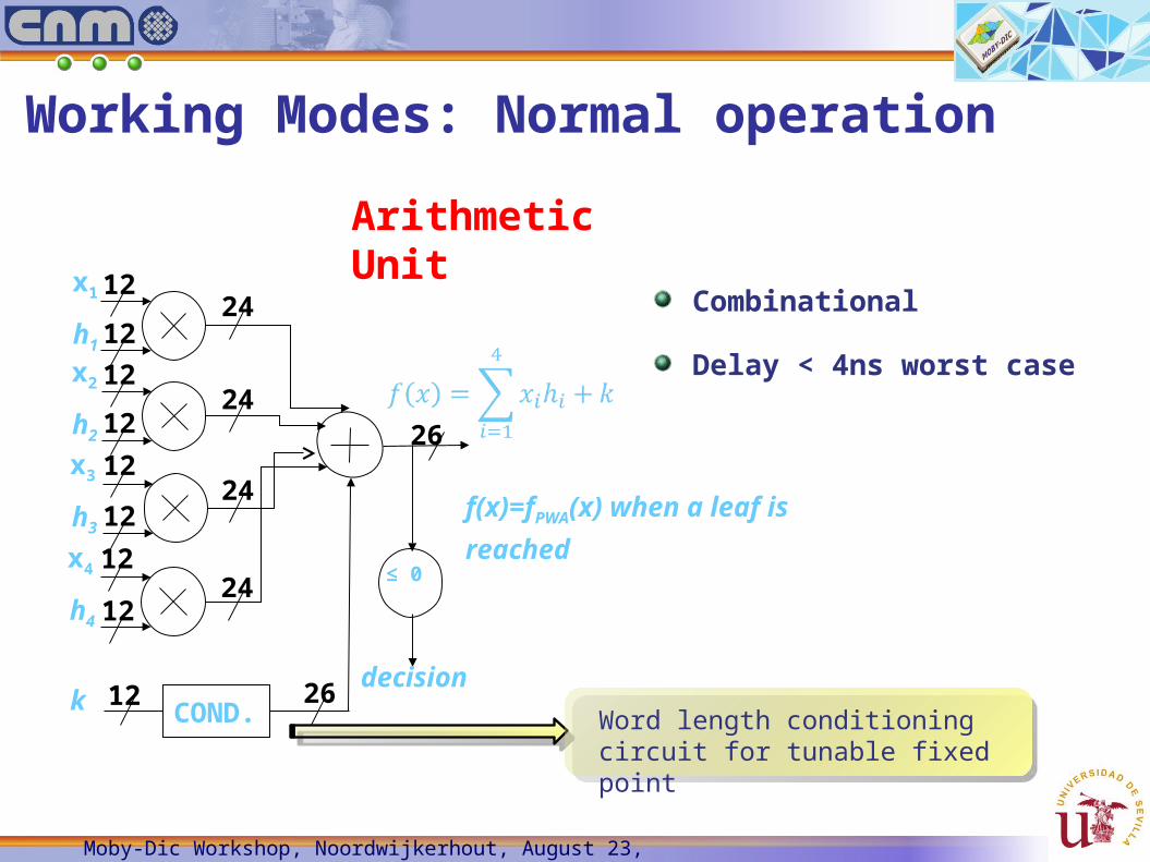
Combinational
Delay < 4ns worst case
Arithmetic Unit
Word length conditioning circuit for tunable fixed point
Working Modes: Normal operation
x1
h1
x2
h2
x4
h4
k
≤ 0
decision
f(x)=fPWA(x) when a leaf is reached
24
24
x3
h3
24
24
26
12
12
12
12
12
12
12
12
12
26
COND.
Moby-Dic Workshop, Noordwijkerhout, August 23, 2012
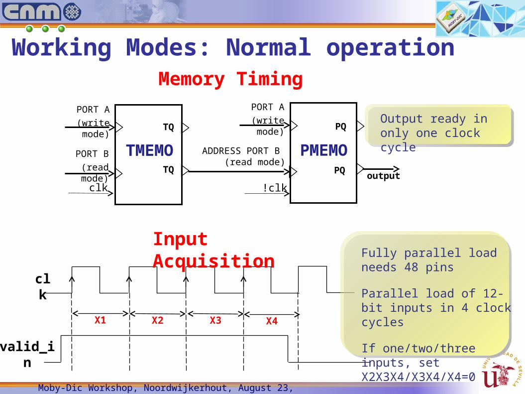
Memory Timing
TMEMO
TQ
TQ
PORT A
(write mode)
PORT B
(read mode)
PMEMO
ADDRESS PORT B (read mode)
outputPQ
PQ
clk !clk
PORT A
(write mode) Output ready in only one clock cycle
X1 X2 X3 X4
Input Acquisition
clk
valid_in
Fully parallel load needs 48 pins
Parallel load of 12-bit inputs in 4 clock cycles
If one/two/three inputs, set X2X3X4/X3X4/X4=0
Working Modes: Normal operation
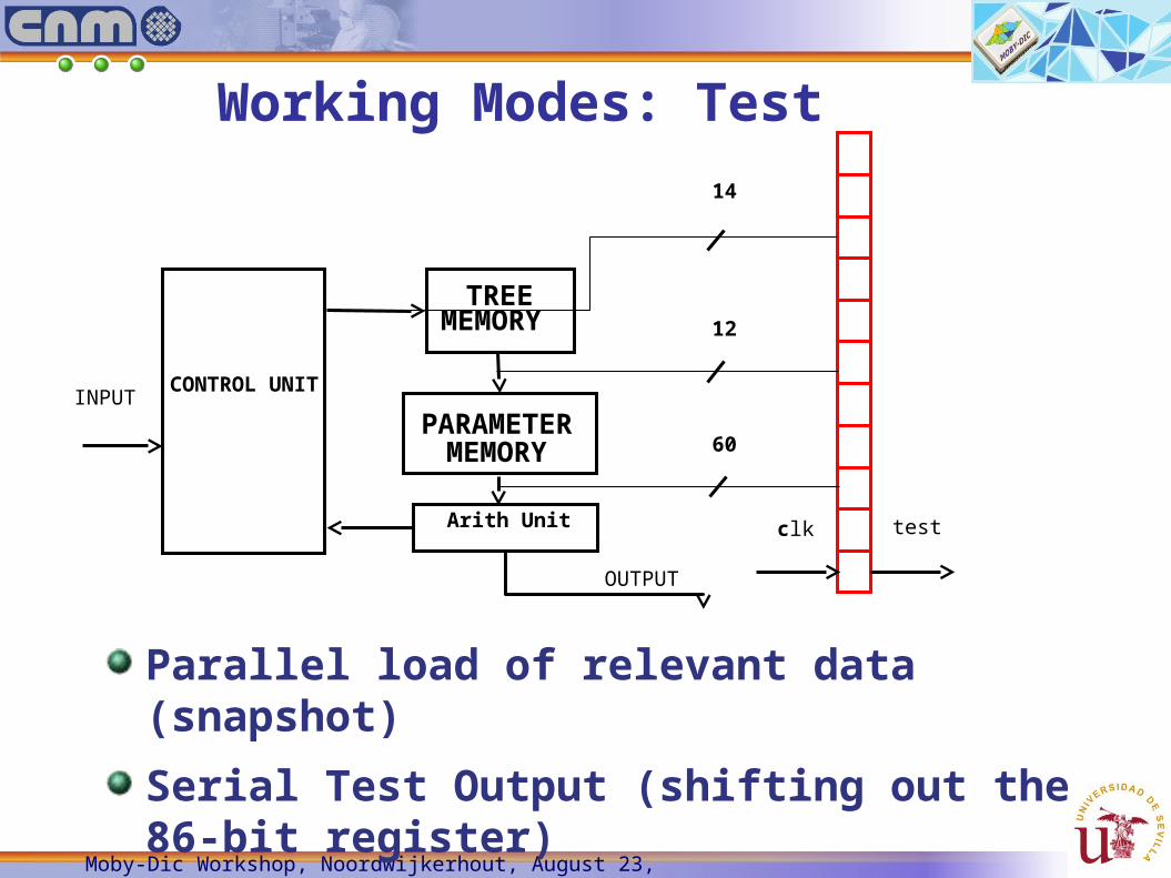
Moby-Dic Workshop, Noordwijkerhout, August 23, 2012
PARAMETER MEMORY
TREE MEMORY
Arith Unit
INPUTCONTROL UNIT
OUTPUT
Parallel load of relevant data (snapshot)
Serial Test Output (shifting out the 86-bit register)
Concurrent to Operation Mode
Working Modes: Test
test
14
12
60
clk
Moby-Dic Workshop, Noordwijkerhout, August 23, 2012
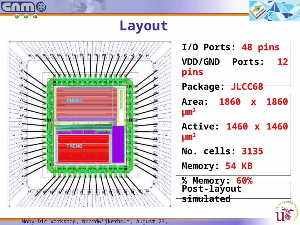
Layout
I/O Ports: 48 pins
VDD/GND Ports: 12 pins
Package: JLCC68
TMEMO
PMEMO Area: 1860 x 1860 µm2
Active: 1460 x 1460 µm2
No. cells: 3135
Memory: 54 KB
% Memory: 60%
Post-layout simulated

Moby-Dic Workshop, Noordwijkerhout, August 23, 2012
Structure of ASIC
Operation mode P=00Writing TMEMO mode P=01Writing PMEMO mode P=10Test mode P=11
No. Inputs: configurable from 1 up to 4No. Outputs: 1Input Resolution: 12 bitsOutput Resolution: 26 bits Parameters Resolution: 12 bitsMaximum No. hyperplanes plus polytopes: 4096Depth of binary search tree: configurable from 1 up to 13Integration technology: 90nm, 2.5V-1.2V, 9 metal layers, TSMC (Taiwan Semiconductor Manufacturing Company)
TMEMO: 16384x12=24KBPMEMO: 4096x60=30KBSize: 1860x1860 µm2
Package: JLCC68

Moby-Dic Workshop, Noordwijkerhout, August 23, 2012
Test Setup of ASIC
Powersupply HPE3630A
LogicAnalyzer Agilent16823A
Experiment controlled with Matlab
Oscilloscope Agilent DSO6104A
Moby-Dic Workshop, Noordwijkerhout, August 23, 2012
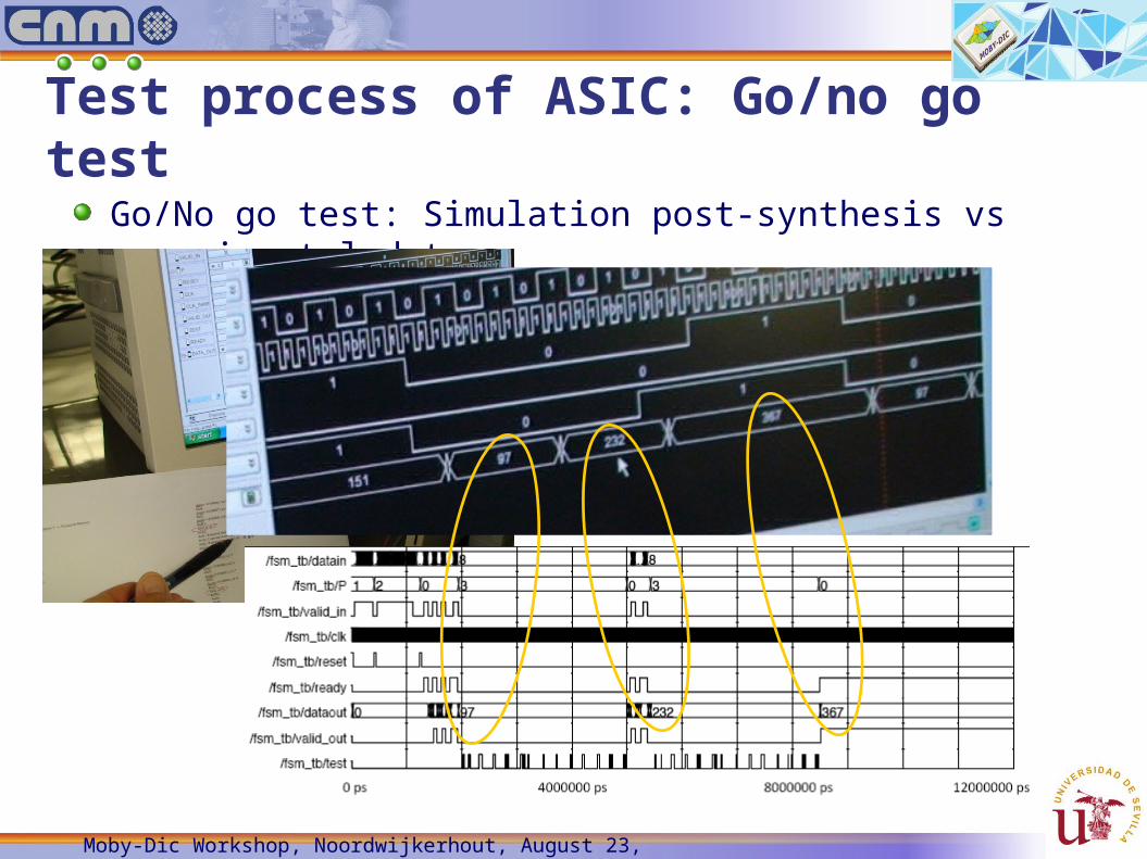
Test process of ASIC: Go/no go test
Go/No go test: Simulation post-synthesis vs experimental data
Moby-Dic Workshop, Noordwijkerhout, August 23, 2012
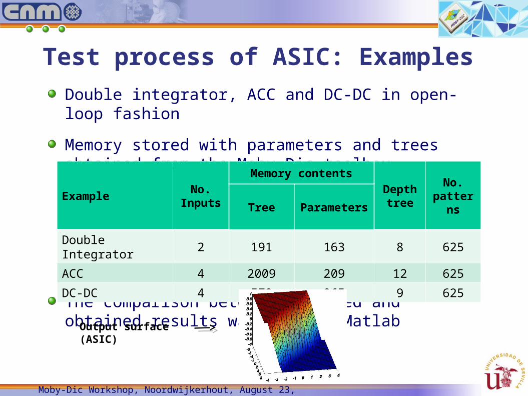
Test process of ASIC: Examples
Double integrator, ACC and DC-DC in open-loop fashion
Memory stored with parameters and trees obtained from the Moby-Dic toolbox
The comparison between expected and obtained results was made by Matlab
ExampleNo.
Inputs
Memory contentsDepthtree
No.patternsTree Parameters
Double Integrator 2 191 163 8 625
ACC 4 2009 209 12 625
DC-DC 4 572 265 9 625
Output surface (ASIC)
Moby-Dic Workshop, Noordwijkerhout, August 23, 2012
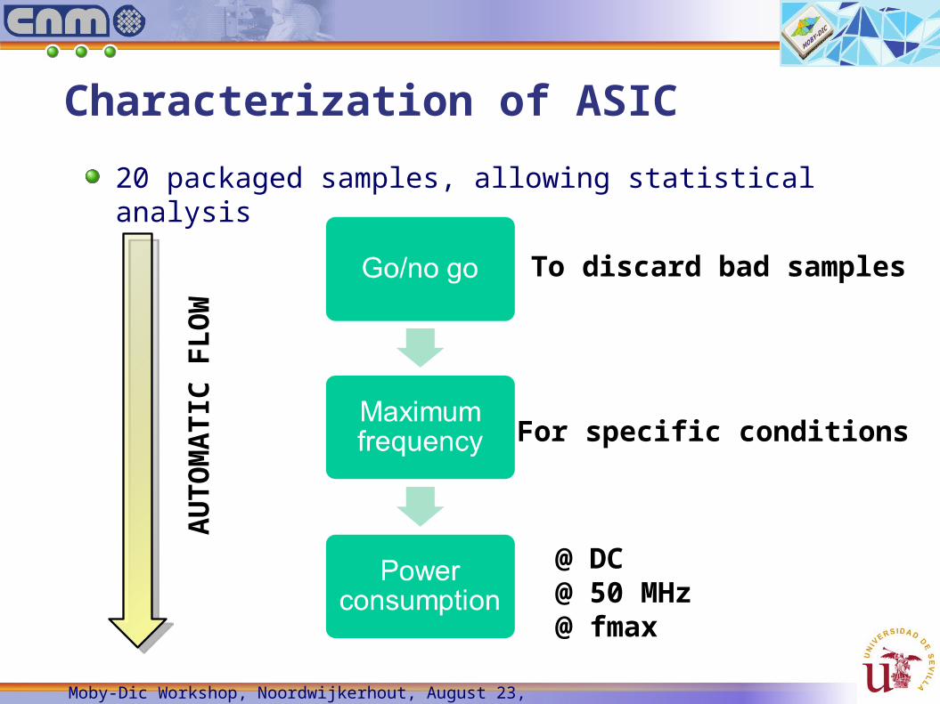
Characterization of ASIC
20 packaged samples, allowing statistical analysis
@ DC@ 50 MHz@ fmax
To discard bad samples
For specific conditions
AU
TO
MA
TIC
FL
OW
Moby-Dic Workshop, Noordwijkerhout, August 23, 2012
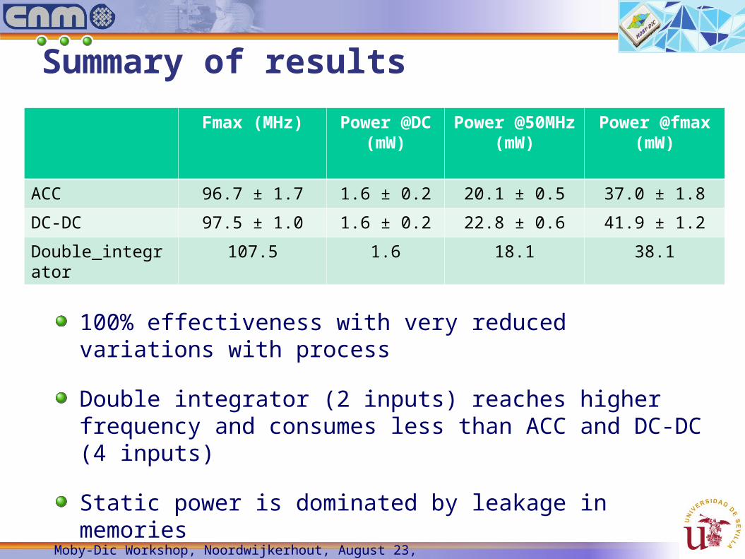
Summary of results
Fmax (MHz) Power @DC (mW)
Power @50MHz (mW)
Power @fmax (mW)
ACC 96.7 ± 1.7 1.6 ± 0.2 20.1 ± 0.5 37.0 ± 1.8
DC-DC 97.5 ± 1.0 1.6 ± 0.2 22.8 ± 0.6 41.9 ± 1.2
Double_integrator 107.5 1.6 18.1 38.1
100% effectiveness with very reduced variations with process
Double integrator (2 inputs) reaches higher frequency and consumes less than ACC and DC-DC (4 inputs)
Static power is dominated by leakage in memories
Moby-Dic Workshop, Noordwijkerhout, August 23, 2012
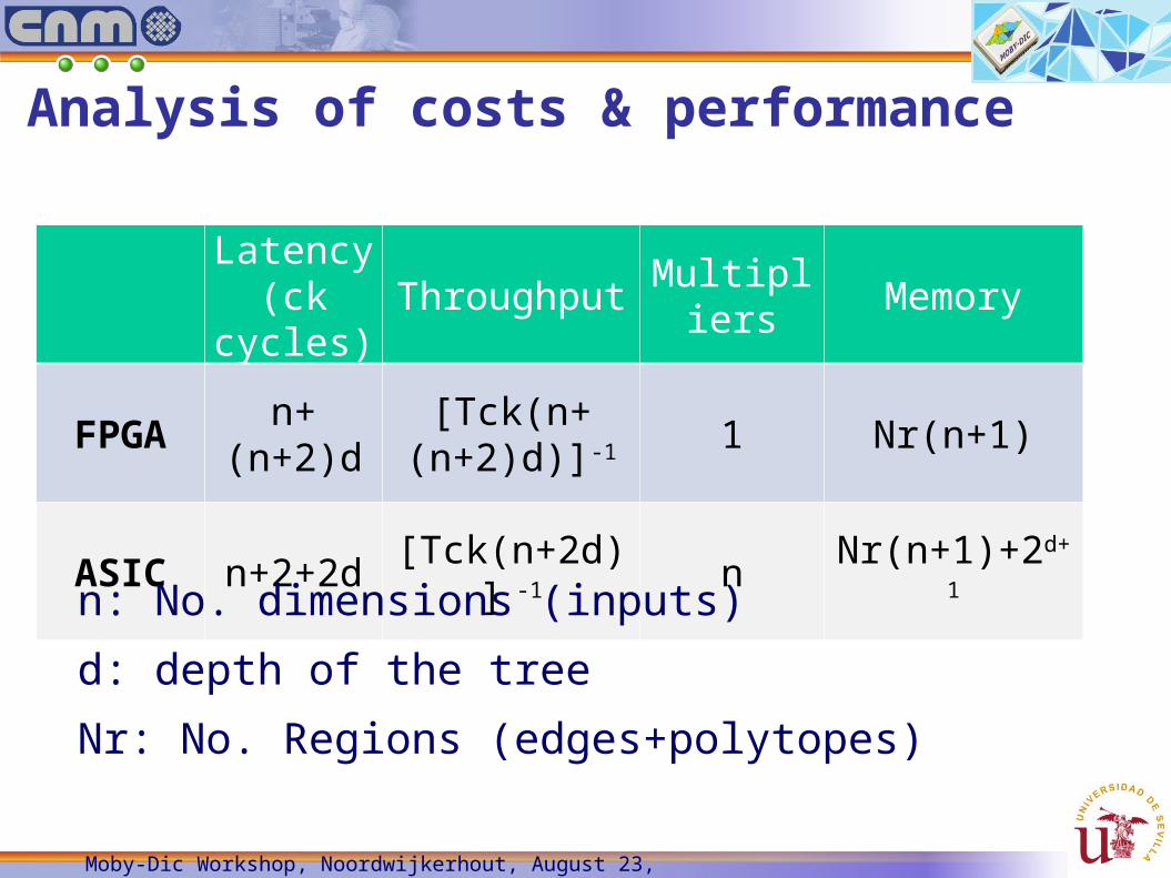
Latency(ck cycles) Throughput Multipliers Memory
FPGA n+(n+2)d [Tck(n+(n+2)d)]-1 1 Nr(n+1)
ASIC n+2+2d [Tck(n+2d)] -1 n Nr(n+1)+2d+1
n: No. dimensions (inputs)
d: depth of the tree
Nr: No. Regions (edges+polytopes)
Analysis of costs & performance

Moby-Dic Workshop, Noordwijkerhout, August 23, 2012
ACC [OLIV11] Archict. Hw
resources Latency Multipliers Memory
FPGAPWAG 87% occup. 2.6 us 1 3.3KB
PWAS-S 31% occup. 390ns 1 11.5KBPWAS-P 95% occup. 67 ns 5 57.6KB
ASIC PWAG 3.5mm2 120-240 ns 4 54KB (27.3KB used)
Post-layout simulation of ASIC provides 4-8 ns for clock cycle
Analysis of cost&performance for CSs
DC-DC Archict. Hw resources Latency Multipliers Memory
FPGAPWAG-S 11% occup. 3.35µs 1 0.59KBPWAG-P 10% occup. 1.15µs 4 0.59KB
ASIC PWAG 3.5mm2 72-144 ns 4 54KB (2.58KB used)
Moby-Dic Workshop, Noordwijkerhout, August 23, 2012
[OLIV09] A. Oliveri, T. Poggi, M. Storace, “Circuit implementation of piecewise-affine functions based on a binary search tree,” European Conference on Circuit Theory and Design (ECCTD’09), pp. 145–148, Antalya, Turkey, August 2009.
[OLIV11] A. Oliveri, G.J.L. Naus, M. Storace, W.P.M.H. Heemels, "Low-complexity approximations of PWA functions: a case study on Adaptive Cruise Control“, European Conference on Circuit Theory and Design (ECCTD'11), pp. 694-697, Linköping, Sweden, August 2011.
References
Moby-Dic Workshop, Noordwijkerhout, August 23, 2012
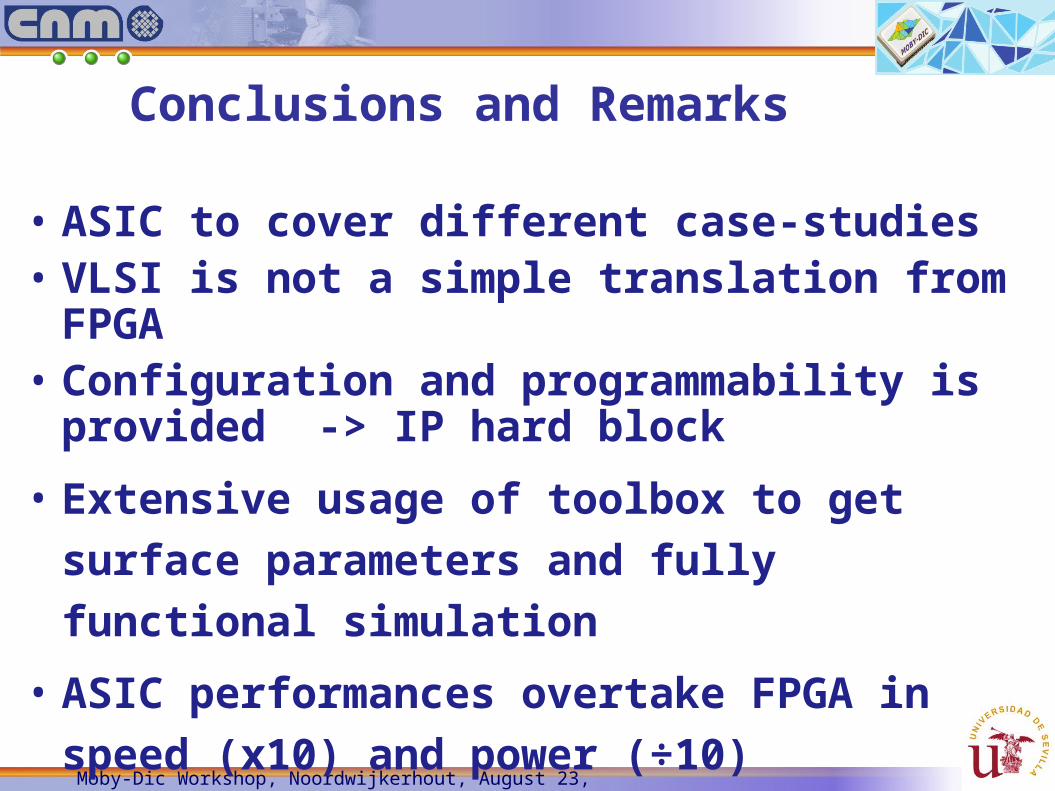
Conclusions and Remarks
• ASIC to cover different case-studies• VLSI is not a simple translation from FPGA • Configuration and programmability is provided -> IP
hard block
• Extensive usage of toolbox to get surface parameters and fully functional simulation
• ASIC performances overtake FPGA in speed (x10) and power (÷10)