Embed Size (px)
Citation preview

mm-wave EM-imaging
Chipless RFID System
Mohammad Zomorrodi
DOCTOR OF PHILOSOPHY
A thesis submitted for the degree of Doctor of Philosophy at
Monash University in 2015
Department of Electrical and Computer Systems Engineering,
Faculty of Engineering,
Monash University, Melbourne, Australia


Copyright notice
© The author (2015). Except as provided in the Copyright Act 1968, this thesis may not be reproduced in any form without the written permission of the author. I certify that I have made all reasonable efforts to secure copyright permissions for third-party content included in this thesis and have not knowingly added copyright content to my work without the owner's permission. Mohammad Zomorrodi


To
My wife
Fatemeh Sajjadi dokht
and my children
MohammadKasra and Zoha Zomorrodi

P a g e | i
Abstract
A new mm-wave imaging chipless RFID system is proposed. The system comprises a
multi-bit tiny chipless RFID tag, a double sided printed dipole array (DSPDA) as the reader
antenna and the synthetic aperture radar (SAR) image processing algorithm. The multi-bit
tags comprise a series of meander line and strip line polarizers on a paper substrate. A
linearly polarized (LP) incident wave illuminates the tag surface at 60 GHz instrumentation
scientific and medical (ISM) band. The DSPDA is a four-element linear array of DSPD
elements. One DSPDA illuminates the tag in vertical polarisation and another DSPDA
receives the backscattered signal in horizontal polarisation. The backscattered signal in the
cross-polar radar cross section (RCS) of the tag contains the data contents. The reader
synthetically processes the cross-polar RCS to construct the image of the tag surface. This
data is decoded in the reader’s synthetic aperture radar (SAR) processor. The developed mm-
wave imaged tag is immune to noise and interference due to its cross polar nature of data
processing. Since the tag does not operate on the frequency signature based principle as is for
its predecessor tags, the new imaged tag provides high data capacity, compact design and
immunity to printing errors.
To validate the concept of the electromagnetic (EM) polariser as the unit cell of the data
encoding element, first, a 45 inclined thin strip line as an effective EM polariser is analysed
using the diffraction theory. The design parameters of the strip line polariser are optimised
for the maximum cross-polar RCS in Computer Simulation Technology (CST) Microwave
Studio full-wave EM solver. The stripline polariser is used to design a few multi-bit first
prototype chipless RFID tags. Knowing the fact that a 45 inclined meander line is an
excellent polariser, secondly, the meander line polariser is investigated for the optimum
cross-polar RCS. It is observed that the meander line polariser provides more compact design
and higher cross-polar RCS compared to that for the stripline polariser. Finally, a few multi-
bit second prototype tags are designed with a series of meander line polarisers.
The advantage of the cross-polar RCS data encoding over the conventional co-polar RCS
data encoding is analysed and then verified through a series of experiments in different
practical scenarios such as tags attached: (i) to an object in cluttered and interfering
environments; (ii) on liquid containers; (iii) on metallic surfaces such as aluminium cans; and

finally, (iv) the tag is covered with thick paper, plywood and cardboard and read at non-line-
of-sight (NLOS) conditions. Moreover, the radius of curvature of a bent tag is thoroughly
investigated attaching the tag on tubes with varying radii. The proposed tag demonstrates
robustness toward multipath and clutter interferences, provides a very reliable approach to
tagging of bent surfaces and highly reflective items such as water bottles and aluminium cans.
Moreover, the mm-wave tag can be read NLOS inside envelopes, cardboard and wooden
boxes hence secure item tagging is also feasible in this approach.
The achieved data encoding capacity of the tag is 2 bits/cm2 which is very promising for
industrial applications. A credit card size tag offers more than 90 bits of data. This content
capacity can be increased further with addition of range resolution image processing of the
tag surface.
The SAR reading process requires movement of the reader antennas around the tag. The
reader takes the snap shots of the whole tag surface at 125 view angles for SAR image
processing. The requirement for relative movement of the reader with respect to the tag is
also addressed with a new multiple input multiple output (MIMO)-based SAR technique. A
limited number of fixed transmit and receive antennas is design based on the MIMO theory to
provide a fast imaging processing for the proposed mm-wave EM-imaging chipless RFID
system. The MIMO signal processing results in significant throughput enhancements in terms
of tag reading time and least hardware requirement.
Finally, the salient features of the proposed system are: (i) a fully printable very compact
tag which costs less than a barcode; (ii) printing error tolerant on-demand commercial
production using a poor quality printer; (iii) low cost lossy substrate materials based
commercial production; (iii) very robust system performance in multipath and cluttered
environments; (iv) very reliable tag readings on liquid containers, reflective and curved
surfaces; (v) the potential to read secured documents/objects hidden in envelopes, wooden
and cardboard boxes; and finally, (vi) very high data encoding capacity. The proposed
chipless RFID tag system finds potentials in low cost item level tagging. Recent success of
Xerox, USA, University Affairs Committee (UAC) Grant of 115, 865 $ from 2015-2017 for
investigations into the proposed tag to read secured documents inside envelops is an excellent
testimonial of the potential of the proposed tag.

P a g e | ii
Declaration
This thesis contains no material which has been accepted for the
award of any other degree or diploma at any university or equivalent
institution and that, to the best of my knowledge and belief, this thesis
contains no material previously published or written by another
person, except where due reference is made in the text of the thesis.
Mohammad Zomorrodi


P a g e | iii
List of publications
Journals:
[1] M.Zomorrodi, and N.C.Karmakar, “ A Low Cost Wideband Printed Dipole Array Antenna
for 60 GHz Image-Based Chipless RFID Reader ”, in IEEE Antennas and Propagation
Magazine, accpeted on 1st Jan 2015, in printing process.
[2] M.Zomorrodi, N.C.Karmakar and J.Walker, “ Fast Imaging Technique for Chipless RFID
Tag “, submitted on 15th Jan 2015 to IEEE Transactions on Microwave Theory and
Techniques as the extended version of IMaRC-2014 conference paper, under review process.
[3] M.Zomorrodi, and N.C.Karmakar, “ Electromagnetic Imaging, a New Power for Chipless
RFID System”, in Cambridge Press, Submitted on Feb 2015.
[4] M.Zomorrodi, and N.C.Karmakar, “mm-Wave Cross-Polar EM-imaging for High Data
Capacity Chipless RFID System “, to IEEE Transactions on Antennas and Propagation,
submitted on 5th June 2015.
[5] M.Zomorrodi, and N.C.Karmakar, “Fast EM-imaging of Chipless RFID System Through
MIMO-based Technique“ to IEEE Transactions on Microwave Theory and Techniques as the
extended version of IMS-2015 conference paper. submitted on 24th June 2015.
Conference papers:
[1] M.Zomorrodi, “Improved Genetic Algorithm Approach for Phased Array Radar Design”, in
Asia-Pacific Microwave Conference, APMC, Melbourne, Australia, 2011.
[2] M. Zomorrodi and N.C.Karmakar, “60 GHz Dipole Array Antenna for SAR-based Chipless
RFID”, in 13th Australian Symposium on Antennas, Sydney, 2013.
[3] M.Zomorrodi, N.C.Karmakar, and S.G.Bansal, “Introduction of Electromagnetic Image-
based Chipless RFID System,” in Intelligent Sensors, Sensor Networks and Information
Processing (ISSNIP-2013), Melbourne, 2013, pp. 443-448.

P a g e | iv
[4] M.Zomorrodi and N.C.Karmakar, “Cross-RCS Based, High Data Capacity, Chipless RFID
System”, in International Microwave Symposium (IMS-2014), Tampa Bay, Flordia, US,
2014.
[5] M.Zomorrodi and N.C.Karmakar, “An Array of Printed Dipoles at 60 GHz”, in IEEE
International Symposium on Antennas and Propagation, Memphis, Tennessee, USA, July-
2014, pp. 73-74.
[6] M.Zomorrodi and N.C.Karmakar, “On the Usage of Diffraction effect for Chipless RFID
Systems”, in Australian Microwave Symposium (AMS), Melbourne, Australia, June 2014.
[7] M.Zomorrodi and N.C.Karmakar, “Cross-Polarized Printable Chipless RFID Tag with
Superior Data Capacity”, in European microwave week, EuMW2014, Rome, Italy, 2014.
[8] M.Zomorrodi and N.Karmakar, “Image-based Chipless RFID System with High Content
Capacity for Low Cost Tagging”, in International Microwave and RF Conference (IMaRC)
Bangalore, India., 2014.
[9] M. Zomorrodi and N.C.Karmakar, “ Fabrication Error Tolerant Array Antenna at 60 GHz”,
in 14th Australian Symposium on Antennas, Sydney, Feb-2015.
[10] M.Zomorrodi and N.C.Karmakar, “ Novel MIMO-based Technique for EM-imaging of
Chipless RFID”, in International Microwave Symposium (IMS- 2015), Phoenix, USA,
May-2015.
[11] M.Zomorrodi and N.C.Karmakar, “On the Study of Fabrication Errors on mm-Wave
Antenna”, in IEEE International Symposium on Antennas and Propagation, Vancouver, BC,
Canada, July-2015.
Grant:
Xerox, USA, University Affairs Committee (UAC) Grant, mm-wave Chipless RFID tag,
$115,865 AUD, 2015-2017.
Investigators, A/P Nemai Chandra Karmakar and Mohammad Zomorrodi, Department of
Electrical and Computer Systems Engineering, Monash University, Clayton, Australia,
Xerox, USA Investigator, Dr. Timothy Stowe, Program Manager, Xerox PARC, Inc, Palo
Alto, CA, USA,

P a g e | v
Remarks: Collaboration with Xerox Ltd, USA is based on the outcomes of this PhD research.
The grant application was ranked in the top 3 proposals among more than 20 shortlisted
applications from reputed universities from all over the world.
Patent:
M.Zomorrodi, N.Karmakar, “MM-Wave Image-based chipless RFID system” Australia
provisional patent, Dec 2013. Patent number: 2013-071.
Book Proposal:
Karmakar, Nemai; Zomorrodi, Mohammad; Divarathne, Chamath, “Advanced Signal
Processing Techniques for Chipless RFID Systems”, John Wiley & Sons, Inc. (Submitted on
September 2014 and approved by Wiley on 3rd
July 2015)
Project Awards and Achievements:
Second place in 3 minutes thesis competition (3MT) at the Postgraduate Research
Forum, Monash University, July 2012.
Second place in poster competition at the Postgraduate Research Forum, Monash
University.
Recipient of the Post publication Award (PPA), Monash University 2015.


P a g e | vi
Acknowledgement
I would like to thank my supervisor A/Prof. Nemai Chandra Karmakar for providing me
the opportunity to work under his supervision. He always provided me all kinds of supports
to complete my PhD research. When I was exhausted, he was the person who generously
supported me. Without his guidance and support, it was not possible to finish this thesis work.
His generous effort on editing my thesis is also highly appreciated. I also thank my associate
supervisor, Prof. Jeffery Walker, the head of Civil Engineering Department, to provide me
the opportunity to get me involved in the SMAP project in the beginning of my PhD
candidature that inspired me toward the EM-imaging technique. Also I thank him for his
guidance during my PhD studies. I would also like to thank other members of my advisory
committee, Prof. Emanuele Viterbo, Dr. Mehmet Rasit Yuce, and Dr. Jonathan Li for their
help on completing my Ph.D. Special thanks also go to my external examiners Prof.
Christophe Fumeaux from Adelaide University and A/Prof. Amin Abbosh from University of
Queensland. Also I thank Dr. Jan Miller for proof reading this dissertation and her useful
suggestions.
The research work and the scholarship have been fully supported by the Australian
Research Council (ARC) Discovery Project Grant: DP110105606: Electronically Controlled
Phased Array Antenna for Universal UHF RFID Applications. I acknowledge ARC’s.
I also would like to express my appreciation to all my colleagues at Monash Microwave,
Antenna, RFID and Sensors (MMARS) laboratory of Monash University. They helped me in
many aspects of my PhD studies. I learnt so many things from them. The daily collaboration
and discussion with my MMARS colleagues provided me tremendous opportunities to
explore different areas of chipless RFID research. Thanks to , Mr. Chamath Divarathne, Drs.
Aminul Islam, Shakil Bhuiyan, Prasanna Kalansuriya, Emran Amin, Mrs. Rubayet-e-azim
Anee, Messer Shuvashis Dey, Muhsiul Hasan and Wan Wan Zamri for their assistances and
pleasant.
My Special thanks to my wife, Mrs. Fatemeh Sajjadi dokht, whose kindness and support
was the most inspirational factor during the PhD studies. It was absolutely her encouragement
to finish my PhD with her love and continues support. I also shall express my special thanks
to my children MohammadKasra and Zoha who endeavoured my absence during my PhD

P a g e | vii
studies and thesis writing. Continues supports and prayers of my beloved parents, Mrs.
Fatemeh Eshraghi and Mr. Hossein Zomorrodi, encouraged me during my entire life
especially during the four years of my PhD studies.

Contents
Chapter 1 Introduction ......................................................................................................................... 1-1
1.1 Barcodes as identification technology ..................................................................................... 1-2
1.2 RFID systems ........................................................................................................................... 1-4
1.3 Barcodes vs RFID .................................................................................................................... 1-5
1.4 Chipless RFID systems ............................................................................................................ 1-6
1.5 Proposed chipless RFID system ............................................................................................... 1-8
1.6 Hypothesis and goals of the research ..................................................................................... 1-12
1.7 Original contributions ............................................................................................................ 1-16
1.8 Thesis outline ......................................................................................................................... 1-17
1.9 Communications of results..................................................................................................... 1-20
Chapter 2 High data capacity, printable chipless RFID tag ............................................................... 2-23
2.1 Introduction ............................................................................................................................ 2-23
2.2 Tag price sensitivity versus applications ............................................................................... 2-23
2.3 Strengthened RFID systems by chipless tags......................................................................... 2-25
2.3.1 Time domain-based chipless RFID systems ..................................................................... 2-26
2.3.2 Frequency domain-based chipless RFID systems ............................................................. 2-28
2.3.3 Phase-domain based and hybrid chipless RFID systems .................................................. 2-32
2.4 EM-imaging in various applications ...................................................................................... 2-34
2.5 Potential advantages of the proposed tag structure ................................................................ 2-35
2.6 Potential advantages of the reader system ............................................................................. 2-38
2.7 Conclusion ............................................................................................................................. 2-41
Chapter 3 EM-imaging through reflective EM-polariser ................................................................... 3-43
3.1 Introduction ............................................................................................................................ 3-43
3.2 Triggered idea by Earth imaging ........................................................................................... 3-45
3.3 Precise scanning of the tag surface ........................................................................................ 3-46
3.3.1 Frequency band selection ................................................................................................ 3-47
3.3.2 Lower printed tag cost at mm-wave ................................................................................ 3-51
3.3.3 Synthetic aperture radar necessity ................................................................................... 3-53
3.4 Tag shaping for unique EM-image purposes ......................................................................... 3-54
3.4.1 Strip line as an EM-polariser .......................................................................................... 3-57
3.4.2 Meander line: a new EM-polariser .................................................................................. 3-65
3.5 Conclusion ............................................................................................................................. 3-69
Chapter 4 Practical data encoding EM-polariser ............................................................................... 4-71
4.1 Introduction ............................................................................................................................ 4-71

4.2 Tag fabrication ....................................................................................................................... 4-72
4.2.1 Photolithographic fabrication process ............................................................................... 4-73
4.2.2 Printing process ................................................................................................................. 4-73
4.3 Measurement and results ........................................................................................................ 4-75
4.3.1 Experimental set-up ........................................................................................................ 4-75
4.3.2 Precise tag results ............................................................................................................ 4-77
4.3.3 Printed tags results .......................................................................................................... 4-78
4.3.4 Cross-polar RCS ............................................................................................................. 4-80
4.4 Discussion on data encoding method ..................................................................................... 4-80
4.4.1 Pros of EM-polarisers ..................................................................................................... 4-80
4.4.2 On/off image-based data encoding algorithm ................................................................. 4-82
4.5 Conclusion ............................................................................................................................. 4-84
Chapter 5 Printed EM-polariser performance ................................................................................. 5-86
5.1 Introduction ............................................................................................................................ 5-86
5.2 System analytical model ........................................................................................................ 5-87
5.3 Effects of multipath interference and clutter .......................................................................... 5-92
5.4 Effect of highly reflective items............................................................................................. 5-94
5.4.1 Liquid container .............................................................................................................. 5-95
5.4.2 Metallic objects ............................................................................................................... 5-96
5.5 None optical LoS tag reading ................................................................................................. 5-98
5.6 Bending effect on tag performance ...................................................................................... 5-101
5.7 Conclusion ........................................................................................................................... 5-105
Chapter 6 Reader antenna ................................................................................................................ 6-107
6.1 Introduction ......................................................................................................................... 6-107
6.2 Technical and operational requirements of the antenna ....................................................... 6-107
6.3 Off-the-shelf products .......................................................................................................... 6-110
6.4 Proposed array of printed dipoles ........................................................................................ 6-111
6.5 Substrate selection and characterisation .............................................................................. 6-113
6.5.1 Substrate selection and thickness .................................................................................. 6-113
6.5.2 Substrate characterisation ............................................................................................. 6-114
6.6 Double side printed dipole ................................................................................................... 6-116
6.6.1 Dipole chamfering......................................................................................................... 6-118
6.6.2 Ground connection tapering .......................................................................................... 6-119
6.6.3 Dipole radiation pattern and cross-polar level .............................................................. 6-121
6.7 Array design ......................................................................................................................... 6-124
6.7.1 Required beamforming array ........................................................................................ 6-124

6.7.2 Corporate feeding network ............................................................................................ 6-125
6.7.3 Mutual coupling ............................................................................................................ 6-128
6.7.4 Extended feedline .......................................................................................................... 6-130
6.8 Measurement results ............................................................................................................ 6-132
6.8.1 Reflection coefficient measurement .............................................................................. 6-133
6.8.2 Antenna fabrication error .............................................................................................. 6-135
6.8.3 Radiation pattern measurement ..................................................................................... 6-138
6.8.4 Gain measurement.......................................................................................................... 6-143
6.9 Conclusion ........................................................................................................................... 6-145
Chapter 7 EM-imaging .................................................................................................................. 7-147
7.1 Introduction .......................................................................................................................... 7-147
7.2 SAR, an effective imaging algorithm .................................................................................. 7-148
7.2.1 SAR versus conventional systems ................................................................................ 7-148
7.2.2 SAR modes of operation ............................................................................................... 7-150
7.3 SAR for chipless RFID ........................................................................................................ 7-152
7.3.1 SAR block diagram ....................................................................................................... 7-152
7.3.2 Range resolution ........................................................................................................... 7-153
7.3.3 Azimuth resolution ........................................................................................................ 7-155
7.4 Tag structure for practical data encoding approach ............................................................. 7-158
7.5 SAR-based signal processing ............................................................................................... 7-161
7.5.1 System structure for data collection .............................................................................. 7-161
7.5.2 Signal processing steps ................................................................................................. 7-162
7.6 Results .................................................................................................................................. 7-165
7.6.1 Proof of concept ............................................................................................................ 7-165
7.6.2 Image resolution versus aperture length ....................................................................... 7-169
7.6.3 High data content tags ................................................................................................... 7-173
7.7 Conclusion ........................................................................................................................... 7-177
Chapter 8 MIMO-based array antenna for fast imaging .................................................................. 8-179
8.1 Introduction .......................................................................................................................... 8-179
8.2 Reader physical movement .................................................................................................. 8-179
8.3 Conventional phased array antenna ..................................................................................... 8-181
8.4 MIMO-based phased array antenna ..................................................................................... 8-184
8.4.1 MIMO-based array theory ............................................................................................ 8-184
8.4.2 MIMO-based array for chipless RFID imaging ............................................................ 8-188
8.4.3 Simulation result ........................................................................................................... 8-192
8.4.4 System optimisation of MIMO-based antenna ............................................................. 8-193

8.5 Conclusion .......................................................................................................................... 8-196
Chapter 9 Conclusion and future works ........................................................................................ 9-197
9.1 Review of the research ......................................................................................................... 9-197
9.2 Addressing the research objective ........................................................................................ 9-198
9.3 Future work .......................................................................................................................... 9-203
9.3.1 Three level-based encoding .......................................................................................... 9-204
9.3.2 Tag orientation sensitivity ............................................................................................. 9-205
REFRENCES ...................................................................................................................................... 208

List of Figures
Figure 1-1 Application areas of identification systems........................................................................ 1-1
Figure 1-2 Data encoding limitation of a 1-D barcode tag due to diffraction effect. ......................... 1-4
Figure 1-3 RFID general system structure. ......................................................................................... 1-5
Figure 1-4 Block diagram of proposed image-based cross-polar chipless RFID system. ................. 1-9
Figure 1-5 Tag structure in image based chipless system. ................................................................. 1-10
Figure 1-6 (a) tag configuration, (b) data encoding method, (c) SAR focused tag image of 101011
tag data. .............................................................................................................................................. 1-12
Figure 1-7 Fulfilling thesis goal. ..................................................................................................... 1-15
Figure 2-1 Expected tag volume versus tag cost. Source: IDTechEx [1]. ........................................ 2-25
Figure 2-2 General classifications of chipless RFID systems. ......................................................... 2-26
Figure 2-3 Time domain-based chipless RFID system, surface acoustic wave (SAW).................... 2-27
Figure 2-4 Working basis of the frequency domain chipless RFID systems. .................................. 2-28
Figure 2-5 Phase-domain based chipless RFID tags. ......................................................................... 2-33
Figure 2-6 Maximum theoretical tag content capacity. ................................................................... 2-37
Figure 2-7 Printed tag with structural anomalies. ............................................................................ 2-38
Figure 2-8 Various measurement scenarios for testing tag performance. ........................................ 2-39
Figure 3-1 Reading schemes in a) conventional RFID system, and b) image-based system. ....... 3-44
Figure 3-2 Flowchart of discussion in Chapter 3. ............................................................................. 3-45
Figure 3-3 Reflection strength based on terrain roughness in earth imaging system [88]. .............. 3-46
Figure 3-4 Reader footprint on tag structure. ................................................................................... 3-48
Figure 3-5 Required 3-dB beamwidth of reader antenna versus reading distance. .......................... 3-49
Figure 3-6 Required antenna aperture size for 1° beamwidth.......................................................... 3-49
Figure 3-7 Specific attenuation due to atmospheric gases [91]. ....................................................... 3-51
Figure 3-8 Tag frequency vs. skin depth in microns for various materials [95]. ............................. 3-52
Figure 3-9 Kurz SECOBO® antennas [96]. ................................................................................... 3-52
Figure 3-10 Initial proposed tag structure based on earth imaging concept. ................................... 3-55
Figure 3-11 Backscattered signals from different types of strips; simulation result. ....................... 3-55
Figure 3-12 Reflection scenario in RFID tag. ................................................................................. 3-56
Figure 3-13 Geometry of diffraction by conductive strip on dielectric slab. .................................. 3-59
Figure 3-14 Co- and cross-polar components of diffracted signals, linear scale. ............................. 3-61
Figure 3-15 Strip orientation for creating cross-polar component, L= 1.45, w= 0.2, ε= 2.55, h=0.0127,
all in mm. ........................................................................................................................................... 3-62
Figure 3-16 Simulated co/cross-polar components of backscattered signal, single stripline , L= 1.45,
w= 0.2, ε= 2.55, h=0.0127, all in mm. ............................................................................................... 3-62
Figure 3-17 a) Five strip lines with same length, b) Simulated co/cross-polar backscattered signals.
........................................................................................................................................................... 3-64
Figure 3-18 Simulated co/cross-polar components of backscattered signal. ................................... 3-65
Figure 3-19 Meander line as transmission EM-polariser. ................................................................ 3-66
Figure 3-20 Multi-layer meander line structure for reflection EM-polariser. ................................. 3-68
Figure 3-21 Simulated co/cross-polar component of single layer stripline and meander line structure.
........................................................................................................................................................... 3-69
Figure 4-1 (a) Strip line polariser, (b) Meander line polariser; all values are in mm..................... 4-72
Figure 4-2 Fabricated EM-polarisers through photolithographic process. ...................................... 4-73
Figure 4-3 SATO printer used for tag printing purpose. ................................................................. 4-74
Figure 4-4 Printed meander line and strip line tags. ......................................................................... 4-75
Figure 4-5 System measurement set up, a) printed strip lines, b) Printed meander lines, c) whole
system, d) Reader antennas. ............................................................................................................... 4-76
Figure 4-6 Measurement result for photolithographic fabricated tags. ............................................ 4-78
Figure 4-7 Measurement results for printed strip and meander line tags. ........................................ 4-79
Figure 4-8 General system structure based on SAR theory. ........................................................... 4-83
Figure 5-1 Schematic block diagram of the chipless RFID system. ................................................. 5-89
Figure 5-2 Severe multipath interference scenario. .......................................................................... 5-93
Figure 5-3 High clutter situation for the tag reading process. .......................................................... 5-93
Figure 5-4 Measurement result for multipath and high clutter situations. ....................................... 5-94
Figure 5-5 Printed meander lines tags attached to a plastic bottle of water. ...................................... 5-96
Figure 5-6 Measured received power level of a printed tag attached to a water bottle.................... 5-96
Figure 5-7 An etched out printed meander lines tag attached to an aluminium can. ....................... 5-97
Figure 5-8 Measured received power level of single layer printed tag attached to a water bottle. .. 5-97
Figure 5-9 NLOS reading scenarios. ................................................................................................ 5-99
Figure 5-10 Effect of various barriers on reading process. ............................................................ 5-100
Figure 5-11 Expected bending on tag length. ................................................................................ 5-102
Figure 5-12 Different paper tubes with varying radii. .................................................................... 5-102
Figure 5-13 Relation between arc angle of attached tag and radius of objects. ............................. 5-103
Figure 5-14 System structure for bending effect measurement. .................................................... 5-104
Figure 5-15 Measurement result based on different tag bending scenarios. .................................. 5-104
Figure 6-1 Required HPBW of the antenna. .................................................................................. 6-109
Figure 6-2 Design flowchart for array of DSPD’s. ........................................................................ 6-113
Figure 6-3 Layout of sample SIW resonator with via holes [24]. .................................................. 6-115
Figure 6-4 Photograph of SIW resonator for dielectric constant and loss tangent measurement of
Taconic TLX-8 [140]. ...................................................................................................................... 6-115
Figure 6-5 Single dipole, Wf = 0.37, FL = 1.05, Fa = 0.55, Wa = 0.19, La = 1, Cd = 0.2 and h = 0.127,
all in mm. ......................................................................................................................................... 6-117
Figure 6-6 Chamfering effect of dipole arms on impedance matching.......................................... 6-119
Figure 6-7 Embedded DSPD antenna with tapered ground connection. ........................................ 6-120
Figure 6-8 Ground connection's effect on matching of dipole. ....................................................... 6-120
Figure 6-9 CST generated 3-D radiation pattern of double side printed dipole (DSPD) antenna. 6-121
Figure 6-10 The DSPD schematic and related E- and H-planes. ................................................... 6-122
Figure 6-11 Simulated radiation pattern (E- and H-planes) of DSPD. .......................................... 6-122
Figure 6-12 Simulated Cross-polar level of single dipole (DSPD). ............................................... 6-123
Figure 6-13 T-junction power divider. ........................................................................................... 6-125
Figure 6-14 T-Junction power divider with a) V-notch b) reactive stub. ................................ 6-126
Figure 6-15 Complete corporate feeding network of array. ........................................................... 6-127
Figure 6-16 The S-parameter of the corporate feeding network of array. ..................................... 6-127
Figure 6-17 Transmission phase of different output ports (S21 and S31) versus frequency for input port
I. ....................................................................................................................................................... 6-128
Figure 6-18 Two adjacent dipoles for mutual coupling measurement. ......................................... 6-129
Figure 6-19 Simulated mutual coupling between adjacent dipoles. ................................................ 6-129
Figure 6-20 An array of 4 DSPD with corporate feeding network. ............................................... 6-130
Figure 6-21 Comparing physical sizes of array antenna and V-type connector. ........................... 6-130
Figure 6-22 Extended CPW feedline and final array structure. ..................................................... 6-132
Figure 6-23 Array and V-type connector considered at simulation step. ....................................... 6-134
Figure 6-24 Reflection coefficient of fabricated array. .................................................................. 6-134

Figure 6-25 Percentage of errors in fabrication process. ............................................................... 6-135
Figure 6-26 Five DSPD arrays and highlighted parametrized sections of array. ........................... 6-137
Figure 6-27 Simulated S11 and five measured return losses of sample arrays. .............................. 6-137
Figure 6-28 System set up for radiation pattern measurement....................................................... 6-138
Figure 6-29 Measured and simulated E-plane radiation pattern, Co- and Cross-polar radiation. .. 6-139
Figure 6-30 Measured and simulated H-plane radiation pattern, Co- and Cross-polar radiation. . 6-141
Figure 6-31 HPBW measurement setup for 1° accuracy. .............................................................. 6-142
Figure 6-32 Measured and simulated HPBW of E-plane in 1° step. ............................................. 6-142
Figure 6-33 Simulated feedline loss of array. ................................................................................ 6-144
Figure 6-34 Measured gain of array. .............................................................................................. 6-144
Figure 7-1 Evolution of conventional radar toward SAR system through array antenna concept. 7-149
Figure 7-2 SAR modes of operation: a) Spotlight mode, b) Stripmap mode. ............................... 7-150
Figure 7-3 Spotlight mode of operation for finer azimuth resolution of chipless RFID tag. .......... 7-151
Figure 7-4 General block diagram of typical SAR-based system [154]. ....................................... 7-152
Figure 7-5 Range resolution concept. ............................................................................................ 7-154
Figure 7-6 Slant and ground range resolutions. ............................................................................. 7-156
Figure 7-7 Ground and slant range resolutions of mm-wave chipless tag. .................................... 7-156
Figure 7-8 Azimuth resolution and required synthetic aperture length. ......................................... 7-158
Figure 7-9 Tag structure and two different reading scenarios. ...................................................... 7-159
Figure 7-10 Image formation processing using RMA [154] ......................................................... 7-164
Figure 7-11 Photograph of 4-bit printed tag. ................................................................................ 7-166
Figure 7-12 Raw SAR signal for tag with data "1001". ................................................................. 7-166
Figure 7-13 Raw SAR signal for tag with data "1011". ................................................................. 7-167
Figure 7-14 EM-image of "1001" tag with 22 cm aperture size, reading range 10 cm. ................ 7-168
Figure 7-15 EM-image of "1011" tag with 22 cm aperture size, reading range 10 cm. ................ 7-168
Figure 7-16 EM-image of the tag "1011" with 12 cm aperture size. ............................................. 7-170
Figure 7-17 EM-image of tag with "1011" data with 17 cm aperture size. .................................. 7-171
Figure 7-18 Final and fundamental aperture length. ...................................................................... 7-172
Figure 7-19 Raw SAR signal and final EM-image of printed tag with 8 bits of data, aperture size 24
cm. .................................................................................................................................................... 7-175
Figure 7-20 Cross-polar EM-image of tag with 11 bits of data, aperture size 27.5 cm. ................ 7-176
Figure 7-21 Cross-polar EM-image of tag with 17 bits of data, aperture size 30 cm. ................... 7-176
Figure 8-1 Stream of discussion in Chapter 8. ............................................................................... 8-180
Figure 8-2 Handheld reader with mechanically moving antennas. ................................................ 8-181
Figure 8-3 General block diagram of phase array antenna. ........................................................... 8-183
Figure 8-4 MIMO-based antenna system and the equivalent sparse array antennas. .................... 8-185
Figure 8-5 MIMO-based antenna and its equivalent virtual array antenna. ................................... 8-187
Figure 8-6 Relative phase shift between one particular Tx antenna and all Rx antennas. ............. 8-188
Figure 8-7 MIMO-based antenna and its equivalent virtual array. ................................................ 8-189
Figure 8-8 MIMO-based antenna for EM-image based chipless RFID system. ............................ 8-193
Figure 8-9 Photograph of a) printed 6-bit tag, b) tag image through normal SAR, c) tag image
through MIMO-based technique. ..................................................................................................... 8-194
Figure 9-1 Two and three level encoding algorithms. ................................................................... 9-205
Figure 9-2 Tag orientation, a) correct angle of 45°, b) mis-oriented tag angle of θ°. .................... 9-206
Figure 9-3 Effect of tag orientation on received signal level. ......................................................... 9-206
Figure 9-4 System degradation due to tag mis-orientation effect. ................................................. 9-207


List of tables
Table 1-1 Barcode, QR codes and RFID [8, 9] ................................................................................ 1-6
Table 3-1 Available spectrum on 60 GHz band .............................................................................. 3-51
Table 5-1 Multiple barrier ................................................................................................................ 5-99
Table 5-2 Dimensions of paper tubes and some well-known items. .............................................. 5-103
Table 6-1 Technical and operational requirements of the reader antenna ....................................... 6-112
Table 6-2 Dielectric parameters of Taconic TLX-8 ........................................................................ 6-116
Table 6-3 3-dB beamwidth of a single DSPD in H-plane .............................................................. 6-123
Table 6-4 3-dB beamwidth of a single DSPD in an E-plane ......................................................... 6-123
Table 6-5 Fabrication variation ...................................................................................................... 6-136
Table 6-6 Simulated and measured HPBW in E-plane .................................................................. 6-142
Table 7-1 Synthetic aperture size and image resolution ................................................................ 7-172
Table 8-1 The MIMO-based advantages ....................................................................................... 8-191

List of Abbreviation
1D One Dimensional
2D Two Dimensional
ADC Analog to Digital Converter
ADS Advanced Design System
ARC Australian Research Council
ASIC Application Specific Integrated Circuit
BW Bandwidth
cm Centimetre
CP Circular polarisation
CPL Cross Polar Ratio
CPU Central Processing Unit
CPW Co-Planar Waveguide
CST Computer Simulation Technology
CW Continuous Wave
DAC Digital to Analog Converter
dpi Dot per inch
DSPD Double side printed dipole
dB Decibel
dBi Gain Expressed in dB with Respect to an Isotropic Radiator
dBm Decibel with milli-watt reference
DGS Defected Ground Structure
DSP Digital Signal Processing/Processor
ECSE Electrical and Computer Systems Engineering
EIRP Equivalent Isotropic Radiated Power
EM Electromagnetic
FCC Federal Communications Commission
FM Frequency Modulated
FSS Frequency Selective Surface
G Gain
GHz Gigahertz
GO Geometric Optic
GTD Geometric Theory of Diffraction
H Henry
HF High Frequency
HPBW Half Power Beamwidth
IC Integrated Circuit
IDT Interdigital Transducer
IF Intermediate Frequency
IL Insertion Loss
ISAR Inverse Synthetic Aperture Radar
ISM Industrial Scientific and Medical
ITU International Telecommunication Union
kHz Kilohertz
LED Light Emitting Diode
LHCP Left Hand Circular Polarisation
LNA Low Noise Amplifier
LO Local Oscillator

LOS Line-of-Sight
LP Linear Polarisation
mA Milliampere
MEC Method of Equivalent Current
MMARS Monash microwave, Antenna, RFID and Sensor research group
MHz Megahertz
MIMO Multiple Input Multiple Output
mm Millimetre
mV Millivolts
nH Nanohenry
PA Power Amplifier
PC Personal Computer
PCB Printed Circuit Board
PCR Pulse Compression Ratio
PO Physical Optic
PNA Performance Network Analyser
PTD Physical Theory of Diffraction
Q Quality Factor
RCS Radar Cross Section
RF Radio Frequency
RFID Radio Frequency Identification
RHCP Right Hand circular Polarisation
RL Return Loss
RLC Resistance-Inductor-Capacitor
RMA Range Migration Algorithm
Rx Receiver
SAR Synthetic Aperture Radar
SAW Surface Acoustic Wave
sec Second
SEM Singularity Expansion Method
SMAP Soil Moisture Active Passive
SNR Signal to Noise Ratio
SRR Split ring Resonator
STD Spectral Theory of Diffraction
TDMA Time Division Multiple Access
TDR Time Domain Reflectometry
TFTC Thin Film Transistor Circuits
TWI Through-to-Wall
Tx Transmitter
UAD Uniform Asymptotic Theory of Diffraction
UHF Ultra-High Frequency
USA United States of America
UTD Uniform Theory of Diffraction
UWB Ultra-Wide Band
V Volt
VCO Voltage Controlled Oscillator
VNA Vector Network Analyser
W Watts

List of Major Symbols
α Weighting aperture coefficient
B Bandwidth
¢ Cent
D Antenna aperture size
F Fourier transform
λ Wavelength
kr Wave number
ρr Range resolution
ρgr Ground range resolution
ρa Azimuth resolution
θ3-dB 3-dB bandwidth
εr Relative dielectric constant
k0 Wave number
Jm Bessel function of order m
σ Scattering parameter
c Velocity of Light in Free Space
Tp Pulse width
γ Chirp rate
P a g e | 1-1
Chapter 1 Introduction
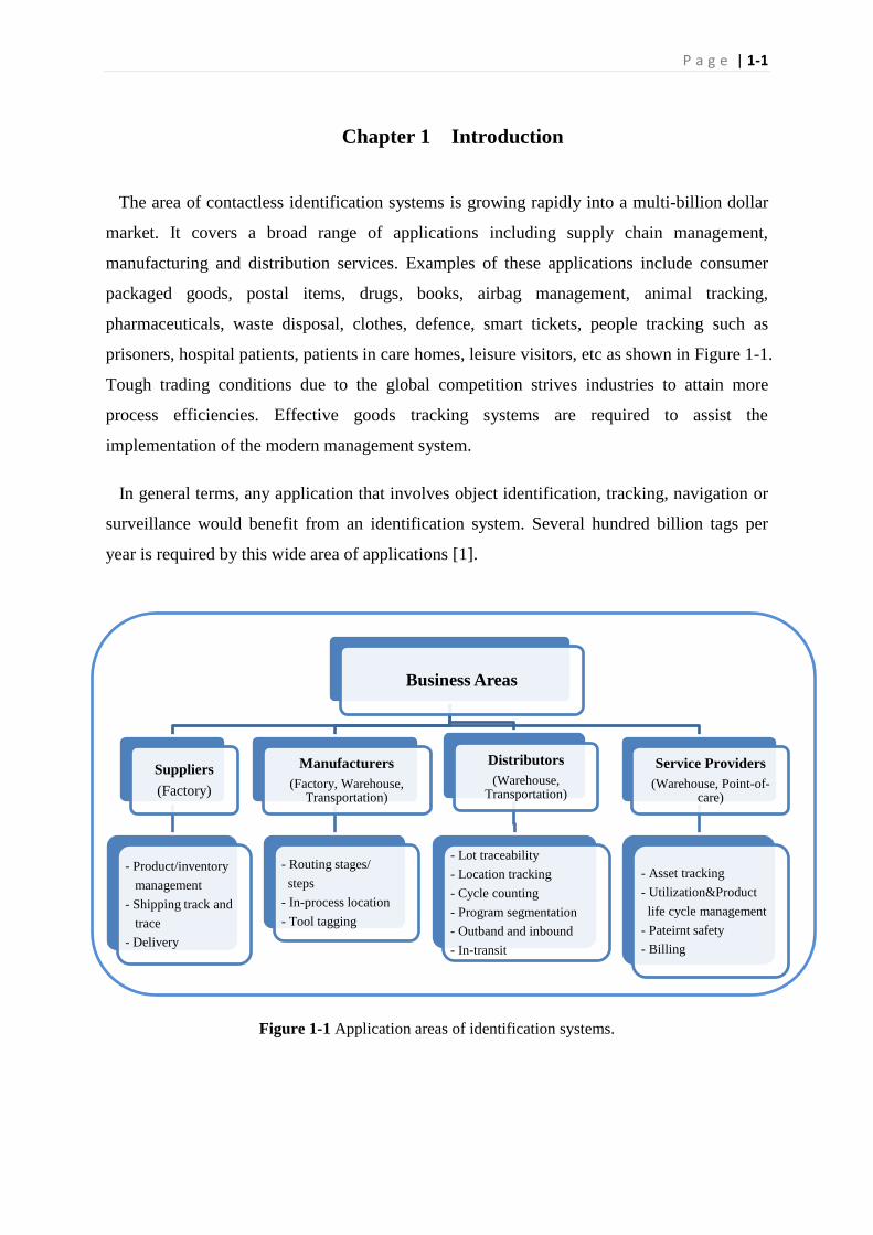
The area of contactless identification systems is growing rapidly into a multi-billion dollar
market. It covers a broad range of applications including supply chain management,
manufacturing and distribution services. Examples of these applications include consumer
packaged goods, postal items, drugs, books, airbag management, animal tracking,
pharmaceuticals, waste disposal, clothes, defence, smart tickets, people tracking such as
prisoners, hospital patients, patients in care homes, leisure visitors, etc as shown in Figure 1-1.
Tough trading conditions due to the global competition strives industries to attain more
process efficiencies. Effective goods tracking systems are required to assist the
implementation of the modern management system.
In general terms, any application that involves object identification, tracking, navigation or
surveillance would benefit from an identification system. Several hundred billion tags per
year is required by this wide area of applications [1].
Figure 1-1 Application areas of identification systems.
Business Areas
Suppliers
(Factory)
- Product/inventory
management
- Shipping track and
trace
- Delivery
Manufacturers
(Factory, Warehouse, Transportation)
- Routing stages/
steps
- In-process location
- Tool tagging
Distributors
(Warehouse, Transportation)
- Lot traceability
- Location tracking
- Cycle counting
- Program segmentation
- Outband and inbound
- In-transit
Service Providers
(Warehouse, Point-of-care)
- Asset tracking
- Utilization&Product
life cycle management
- Pateirnt safety
- Billing
P a g e | 1-2
In this market, every application has its own technical and financial specifications. Main
applications, those that need a huge number of tags, require high data encoding capacity and
survive only with a very cheap tag solution. For others, secure identification and anti-theft
tagging is more important. In some cases, the tag size is a key factor and for some others
proper identification of highly reflective items like liquid containers or metal objects has
more priority. Reading range is also another important factor for many applications.
Irrespective of all priorities, there are two main factors which matter in all applications, the
data encoding capacity and the system cost. For applications with millions of items for
tagging, high data capacity of the identification system is a must. However, for applications
with a limited number of objects, high data encoding capacity may be utilised for secure and
higher reading reliability by sacrificing some of the available data bits. Moreover, cost
reduction is the main initiative for the usage of identification systems in industry. Obviously,
the cost of the identification system and its tagging price must be low and competitive
enough to initiate the request for the system. Otherwise, there would be no demand for such
systems.
The cost of identification systems, like any other broadcasting service, has two parts: the
reader and the tag. The reader cost is normally a fixed cost irrespective of the number of tags.
However, the price of the tag attached to every individual item is the most costly part of the
whole system. Specifically when the number of items are in the order of millions, then the tag
cost plays a major role in the system’s total cost. For such applications, a tag cost of only one
dollar would increase the total cost of the system to a level that restricts the usage of
identification systems. Therefore, the tag price should be kept as small as possible to offer a
reasonably low identification system cost.
1.1 Barcodes as identification technology
The barcode is an optical-based, machine-readable technique for identification purposes. It
has been established in various industries for many decades with proven applicability. It
provides an extremely low cost solution for identification of items to which it attaches.
Originally, barcode tags are comprised of many parallel printed dark lines. The tag’s data are
systematically represented by varying the widths and spacing of those parallel lines. This type
of barcode, dominant in many applications, is normally referred to as a linear or one
dimensional (1-D) barcode. Data encoding capacity of the barcode tag is restricted by the
P a g e | 1-3
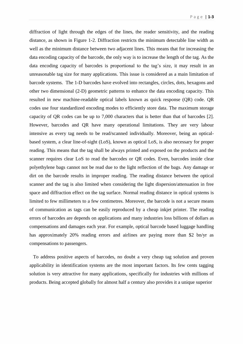
diffraction of light through the edges of the lines, the reader sensitivity, and the reading
distance, as shown in Figure 1-2. Diffraction restricts the minimum detectable line width as
well as the minimum distance between two adjacent lines. This means that for increasing the
data encoding capacity of the barcode, the only way is to increase the length of the tag. As the
data encoding capacity of barcodes is proportional to the tag’s size, it may result in an
unreasonable tag size for many applications. This issue is considered as a main limitation of
barcode systems. The 1-D barcodes have evolved into rectangles, circles, dots, hexagons and
other two dimensional (2-D) geometric patterns to enhance the data encoding capacity. This
resulted in new machine-readable optical labels known as quick response (QR) code. QR
codes use four standardized encoding modes to efficiently store data. The maximum storage
capacity of QR codes can be up to 7,000 characters that is better than that of barcodes [2].
However, barcodes and QR have many operational limitations. They are very labour
intensive as every tag needs to be read/scanned individually. Moreover, being an optical-
based system, a clear line-of-sight (LoS), known as optical LoS, is also necessary for proper
reading. This means that the tag shall be always printed and exposed on the products and the
scanner requires clear LoS to read the barcodes or QR codes. Even, barcodes inside clear
polyethylene bags cannot not be read due to the light reflection of the bags. Any damage or
dirt on the barcode results in improper reading. The reading distance between the optical
scanner and the tag is also limited when considering the light dispersion/attenuation in free
space and diffraction effect on the tag surface. Normal reading distance in optical systems is
limited to few millimeters to a few centimetres. Moreover, the barcode is not a secure means
of communication as tags can be easily reproduced by a cheap inkjet printer. The reading
errors of barcodes are depends on applications and many industries loss billions of dollars as
compensations and damages each year. For example, optical barcode based luggage handling
has approximately 20% reading errors and airlines are paying more than $2 bn/yr as
compensations to passengers.
To address positive aspects of barcodes, no doubt a very cheap tag solution and proven
applicability in identification systems are the most important factors. Its few cents tagging
solution is very attractive for many applications, specifically for industries with millions of
products. Being accepted globally for almost half a century also provides it a unique superior
P a g e | 1-4
Figure 1-2 Data encoding limitation of a 1-D barcode tag due to diffraction effect.
opportunity that makes it very difficult for other technologies to compete. The globally
accepted international barcode quality specification standards, ISO/IEC-15416 (linear) and
ISO/IEC 15415 (2-D) [3], and no privacy issues involved with the barcodes usage are highly
regarded by many users. Moreover, barcode systems provide a fairly good reading accuracy
that is almost comparable with what other new techniques are offering [3]. Another good
aspect of the barcode is that the accuracy of the reading process is almost independent of the
items on which tags are placed.
1.2 RFID systems
The usage of light waves as a communication means between the reader and the tag in
barcode systems causes many technical and operational limitations. Diffraction of light waves
by the barcode lines restricts the data encoding capacity and its reading distance. Barcodes
also require a clear LoS for proper reading. Labour intervention is another major limitation of
the barcodes systems. As an alternative approach, the use of EM-waves for identification and
tracking of objects was first proposed by Watson-Watt in 1935 [4] and coined as the Radio
Frequency Identification (RFID) system. In an RFID system, the reader sends an EM-wave
interrogating signal toward the tag. This signal is then processed by the tag’s microchip unit
and backscattered towards the reader. This backscattered signal carries the tag identification
information and is received and processed by the reader to retrieve the data.
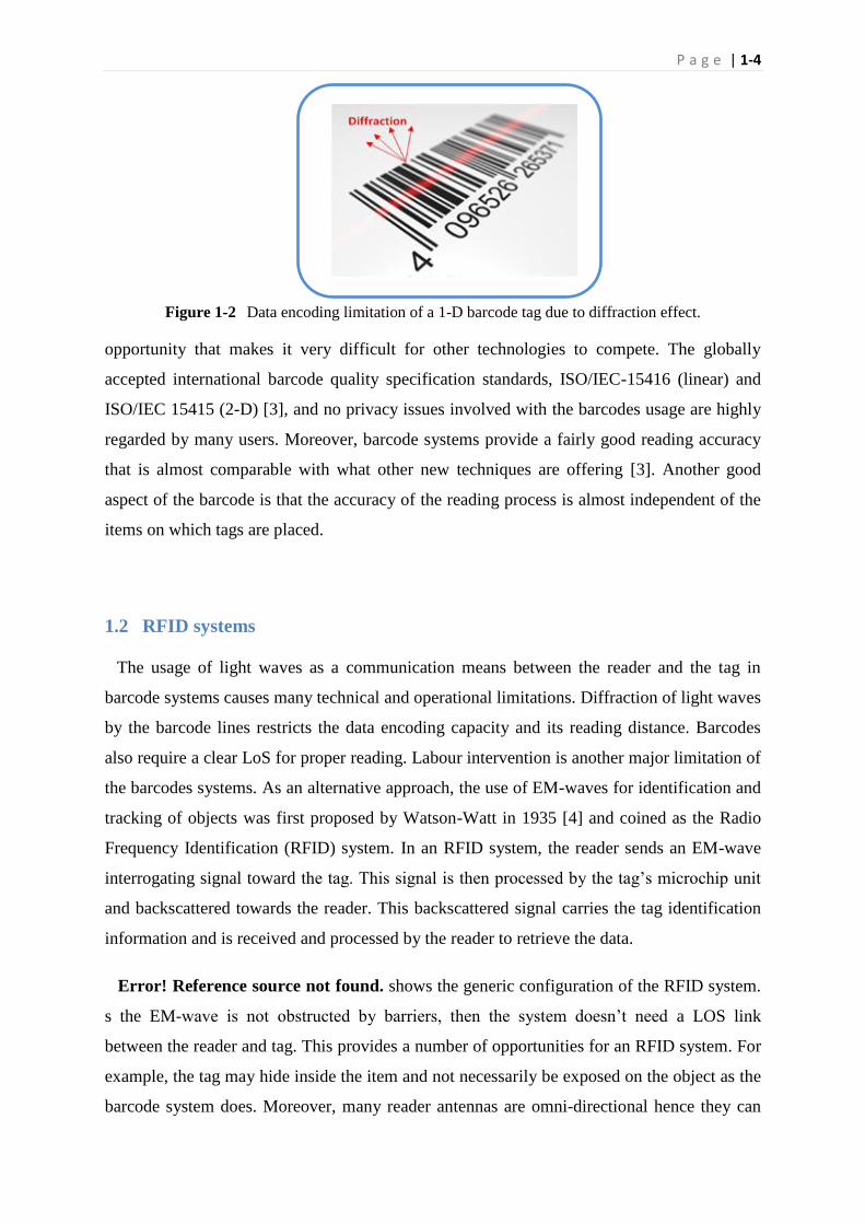
Error! Reference source not found. shows the generic configuration of the RFID system.
s the EM-wave is not obstructed by barriers, then the system doesn’t need a LOS link
between the reader and tag. This provides a number of opportunities for an RFID system. For
example, the tag may hide inside the item and not necessarily be exposed on the object as the
barcode system does. Moreover, many reader antennas are omni-directional hence they can
P a g e | 1-5
detect tags irrespective of their position with respect to the reader. Multiple tag reading is also
feasible in an RFID system, bulk detection scenario. The RFID reading distance may be
much greater than that of barcodes as the EM-waves are much less attenuated in free space
than light waves. The more attractive part of an RFID system is its higher data encoding
capacity, which is not comparable to the barcode, as the data are encoded by a microchip.
Moreover, many security codes can be easily manipulated inside the microchip to provide
more secure communication.
Figure 1-3 RFID general system structure.
1.3 Barcodes vs RFID
Optical based identification systems such as barcodes and QR Codes, and RFID systems all
have their own advantages and limitations. This means that each system would be suitable for
different purposes and under different circumstances. Although majority of users still
consider barcode systems as the most cost effective way to handle the circulation and
inventory management of equipment, the indication of changing market occurred in 2003,
when Walmart adopted and mandated RFID tagging for all its suppliers. Walmart's motto of
mandating RFID is to obtain seamless information from the manufacturing point to the ends
of sales when the goods are sold and the boxes are crashed. There are numerous discussions
and studies in industry and academia about the suitability of these three systems [5-9]. It is
almost agreed that there is no clear superiority of one technology over other technology when
the cost and operational flexibility both are considered simultaneously. In general, it is upon
each specific industry to select the most suitable technology based on their needs and budgets.
The benefit of barcode technology comes from their low cost implementation. It is well
established in industry and has fairly enough content capacity for many industrial and
RFID tag
RFID reader
Control unitWeb
P a g e | 1-6
commercial applications. QR codes offering higher data encoding capacity while working
almost on the same basis as barcodes. RFID are popular and appropriate technology than
barcodes for many industries as it can provide higher content capacity and much more
operational flexibilities. As for example, Cisco recently announced its new idea of internet-
of-everything (IoE) based on RFID systems [10]. However, conventional RFID systems are
associated with limitations too. The main issue for RFID is that many industries cannot afford
the cost. To alleviate the potentials of RFID systems to compete with optical barcodes and
being accepted by more applications, it is required to reduce the cost of the RFID tag to a
level similar to optical barcodes, say less than a cent. A fully printable tag which is still able
to provide the same or higher data encoding capacity compared to 1-D barcodes with more
operational flexibility would be highly welcomed by industries.
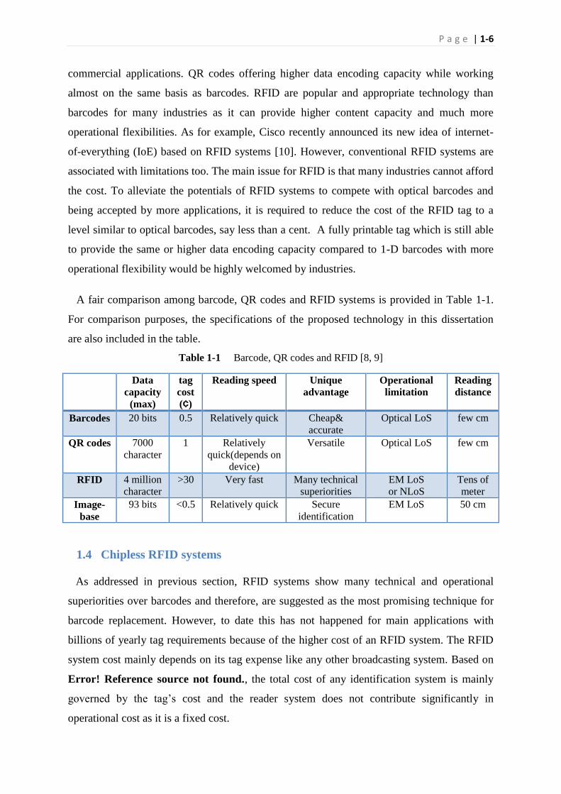
A fair comparison among barcode, QR codes and RFID systems is provided in Table 1-1.
For comparison purposes, the specifications of the proposed technology in this dissertation
are also included in the table.
Table 1-1 Barcode, QR codes and RFID [8, 9]
Data
capacity
(max)
tag
cost
(¢)
Reading speed Unique
advantage
Operational
limitation
Reading
distance
Barcodes 20 bits 0.5 Relatively quick Cheap&
accurate
Optical LoS few cm
QR codes 7000
character
1 Relatively
quick(depends on
device)
Versatile Optical LoS few cm
RFID 4 million
character
>30 Very fast Many technical
superiorities
EM LoS
or NLoS
Tens of
meter
Image-
base
93 bits <0.5 Relatively quick Secure
identification
EM LoS 50 cm
1.4 Chipless RFID systems
As addressed in previous section, RFID systems show many technical and operational
superiorities over barcodes and therefore, are suggested as the most promising technique for
barcode replacement. However, to date this has not happened for main applications with
billions of yearly tag requirements because of the higher cost of an RFID system. The RFID
system cost mainly depends on its tag expense like any other broadcasting system. Based on
Error! Reference source not found., the total cost of any identification system is mainly
governed by the tag’s cost and the reader system does not contribute significantly in
operational cost as it is a fixed cost.
P a g e | 1-7
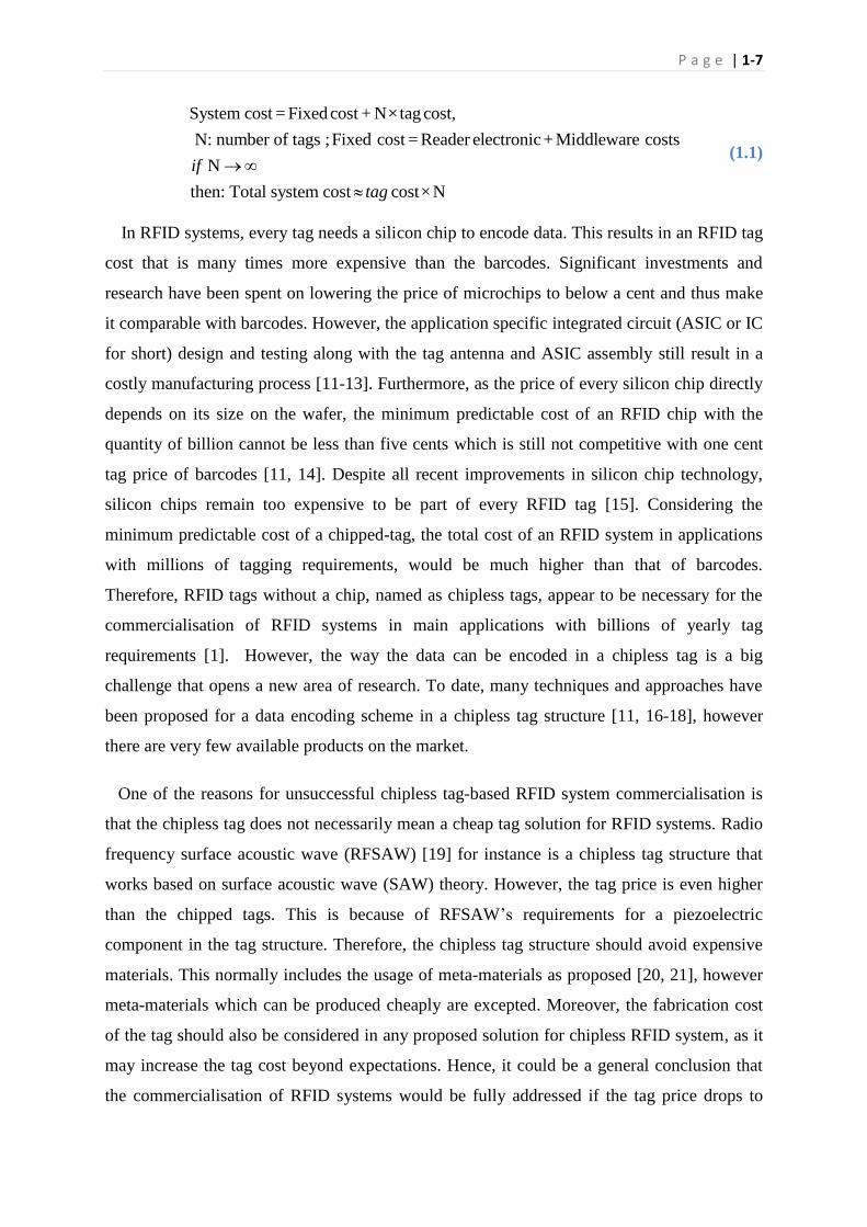
System cost = Fixed cost + N×tag cost,
N: number of tags ;Fixed cost = Reader electronic+ Middleware costs
N
then: Total system cost cost×N
if
tag
(1.1)
In RFID systems, every tag needs a silicon chip to encode data. This results in an RFID tag
cost that is many times more expensive than the barcodes. Significant investments and
research have been spent on lowering the price of microchips to below a cent and thus make
it comparable with barcodes. However, the application specific integrated circuit (ASIC or IC
for short) design and testing along with the tag antenna and ASIC assembly still result in a
costly manufacturing process [11-13]. Furthermore, as the price of every silicon chip directly
depends on its size on the wafer, the minimum predictable cost of an RFID chip with the
quantity of billion cannot be less than five cents which is still not competitive with one cent
tag price of barcodes [11, 14]. Despite all recent improvements in silicon chip technology,
silicon chips remain too expensive to be part of every RFID tag [15]. Considering the
minimum predictable cost of a chipped-tag, the total cost of an RFID system in applications
with millions of tagging requirements, would be much higher than that of barcodes.
Therefore, RFID tags without a chip, named as chipless tags, appear to be necessary for the
commercialisation of RFID systems in main applications with billions of yearly tag
requirements [1]. However, the way the data can be encoded in a chipless tag is a big
challenge that opens a new area of research. To date, many techniques and approaches have
been proposed for a data encoding scheme in a chipless tag structure [11, 16-18], however
there are very few available products on the market.
One of the reasons for unsuccessful chipless tag-based RFID system commercialisation is
that the chipless tag does not necessarily mean a cheap tag solution for RFID systems. Radio
frequency surface acoustic wave (RFSAW) [19] for instance is a chipless tag structure that
works based on surface acoustic wave (SAW) theory. However, the tag price is even higher
than the chipped tags. This is because of RFSAW’s requirements for a piezoelectric
component in the tag structure. Therefore, the chipless tag structure should avoid expensive
materials. This normally includes the usage of meta-materials as proposed [20, 21], however
meta-materials which can be produced cheaply are excepted. Moreover, the fabrication cost
of the tag should also be considered in any proposed solution for chipless RFID system, as it
may increase the tag cost beyond expectations. Hence, it could be a general conclusion that
the commercialisation of RFID systems would be fully addressed if the tag price drops to
P a g e | 1-8
below one cent, including the cost of fitting them in place. This encourages researchers to
work on the printable tag structure for reduction of the fabrication cost to the barcode level.
However, any proposed tag structure must be able to provide the required encoding capacity
in a small tag size. There are examples of chipless and printable tag solutions but the
expected data capacity leads to an un-reasonable tag size [22].
The last but very important criterion for a successful chipless RFID system is its proven
performance based on the commercialised tag structure. There are many proposed prototypes
available in the open literature with very good performance that is based on the precisely
fabricated tag and through using high quality copper and low loss materials as the substrate.
However, if the proposed tag structure is printed on paper by a low cost conductive inkjet
printer, the overall performance of the tag drops significantly. Normally, the frequency
domain-based chipless RFID systems fall in this category [22-26]. Any proposal for a
chipless tag with proven performance and high data encoding capacity, based on the printed
version of the tag structure, would revolutionise the multi-billion dollar market of the
identification and tracking industries.
1.5 Proposed chipless RFID system
This research introduces a new data encoding scheme for the chipless RFID systems. The
EM-imaging in the mm-wave range is proposed for data retrieval from a chipless tag. The tag
is comprised of tiny conductive printable strip or meander lines as EM-polarisers. The EM-
polarisers on the tag surface create a high cross-polar radar cross section (RCS) on the
backscattered signal while being interrogated by a linearly polarised signal. The reader
utilises two orthogonally oriented arrays of double side printed dipole (DSPD) antennas [27,
28]. The reader moves around the tag to create a synthetic aperture and provides a fine EM-
image of the tag using synthetic aperture radar (SAR) signal processing. Figure 1-4 shows the
general structure of the reader, the tag and the movement requirement in the proposed system.
In comparison to other techniques in chipless RFID systems, the tag structure is fully
passive and printable. The expected tag printing cost is even less than that of barcodes as the
tag size in the proposed technique is smaller than the barcodes. The system does not require
any calibration or reference tag. Changing the background of the environment around the tag
has no effect on the performance of the proposed system.

P a g e | 1-9
Figure 1-4 Block diagram of proposed image-based cross-polar chipless RFID system.
It also provides higher data encoding capacity in a smaller tag size as reported to date by
other chipless RFID systems [18, 29, 30]. The system is very robust to multipath and clutter
interference as it is a cross-polar based system. Moreover, the highly reflective items tagged
with the proposed tag structure show a very satisfactory result. All printing inaccuracies are
also considered in the proposed system and appropriate solutions are suggested. All the
measurements of the system are based on the printed tag structure in a highly reflective lab
environment with no calibration process.
The proposed frequency band of operation is the licence free band of 57-64 GHz. However,
working on higher frequency bands is also possible. The global regulatory freedom [31-34] of
the 57-64 GHz, equivalent isotropic radiated power (EIRP) < 40 dBm, provides a unique
opportunity for a reading distance of up to one metre. This is again an enhancement
compared with other available chipless RFID techniques. The system does not require any
ultra wide band (UWB) reader as the data are not encoded in the frequency domain of the
backscattered signal. Moreover, no narrow pulsed shape for the interrogation signal is needed
as the data are not encoded in the time response of the tag. The receiver simply sends a
chirped wave signal and the detection of the tag’s ID is based on the EM-image of the tag in a
cross-polar direction. This suggests a simple receiver structure; however the physical
RX
Synthetic aperture
V-polarised
wave
Chipless tag
TX
H-polarised
wave
Meander line or
strip line
V-polarised DSPD
H-polarised DSPD
Reader
Position-1
Position-n
Position-N
P a g e | 1-10
movement of the reader and SAR-based signal processing are required at this stage of the
research.
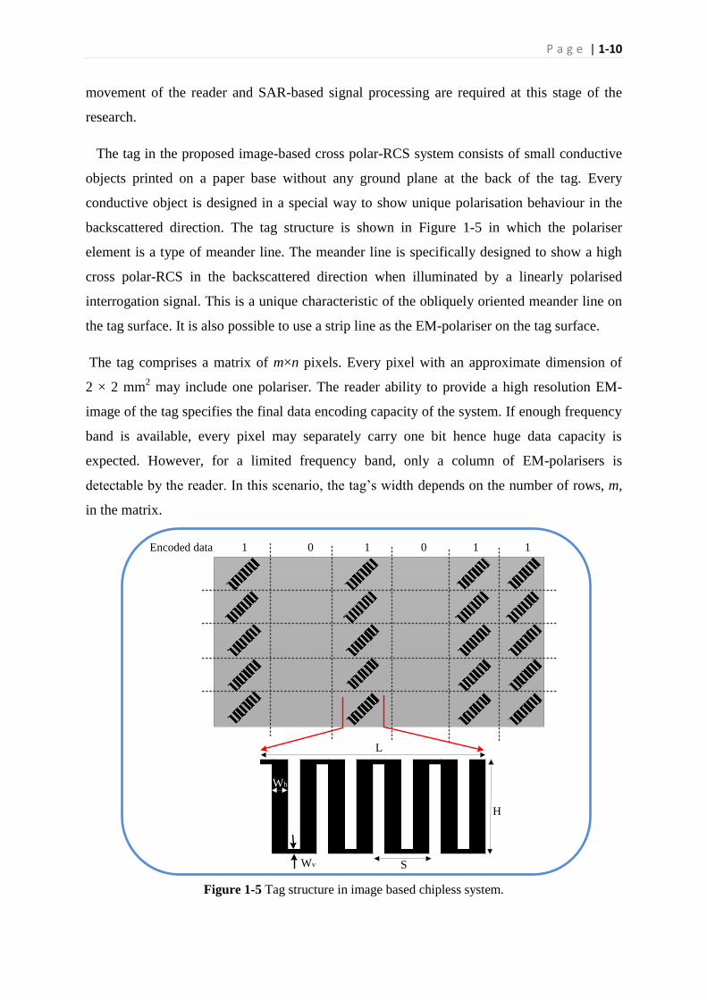
The tag in the proposed image-based cross polar-RCS system consists of small conductive
objects printed on a paper base without any ground plane at the back of the tag. Every
conductive object is designed in a special way to show unique polarisation behaviour in the
backscattered direction. The tag structure is shown in Figure 1-5 in which the polariser
element is a type of meander line. The meander line is specifically designed to show a high
cross polar-RCS in the backscattered direction when illuminated by a linearly polarised
interrogation signal. This is a unique characteristic of the obliquely oriented meander line on
the tag surface. It is also possible to use a strip line as the EM-polariser on the tag surface.
The tag comprises a matrix of m×n pixels. Every pixel with an approximate dimension of
2 × 2 mm2 may include one polariser. The reader ability to provide a high resolution EM-
image of the tag specifies the final data encoding capacity of the system. If enough frequency
band is available, every pixel may separately carry one bit hence huge data capacity is
expected. However, for a limited frequency band, only a column of EM-polarisers is
detectable by the reader. In this scenario, the tag’s width depends on the number of rows, m,
in the matrix.
Figure 1-5 Tag structure in image based chipless system.
L
H
Wh
Wv S
Encoded data 1 1 1100
P a g e | 1-11
Normally, 5~10 polarisers are required to produce adequate RCS levels for 50 cm to 100
cm reading distance. However the reading distance also depends on the transmit power and
reader sensitivity. Consequently, the tag’s width is fixed and varies between 5-15 mm. Every
column of the tag surface may include the total number of m polarisers for data bit “1” or it
may have no polariser for data bit “0”. Figure 1-5 shows the structure of a tag with the data
content of “101011”. When the moving reader finishes a full synthetic aperture scan, the
effect of each vertical slice of the tag is separately analysed by the signal processing. Based
on the presence or absence of the polarisers, the reader then receives a significantly different
power level, ΔRCS = 20 dB for example, on the cross-polar RCS.
This RCS difference ensures data encoding at this mm-wave frequency band. Absence or
presence of vertical polariser-strips yields RCS variation that represents “ 0 ” and “ 1 ”
binary bits respectively as the encoding algorithm. The received power level on the cross-
polar direction is shown in Figure 1-6 that depends on the presence or absence of polariser(s)
on each vertical slice of the tag surface. The 20 dB different level is the minimum measured
level for a printed tag structure. This detected power level difference is reliably transferable
to the EM-image of the tag. The calculated EM-image of the tag through SAR-based signal
processing is also shown in Figure 1-6(c).
The width of each vertical slice of the tag structure which carries one bit of data is only 2
mm. Multiple vertical columns of polariser-strips in a matrix configuration yield a multi-bit
tag design. This means that encoding capacity of the system is proportional to the tag’s length
while its width is fixed and depends mainly on the expected reading distance. Since 60 GHz
strips are mini-scale structures, large data bits can be included in a credit card size chipless
tag. As for example, a 100 × 7 mm2 tag area is capable of encoding up to 50 or more bits of
binary data.

P a g e | 1-12
Figure 1-6 (a) tag configuration, (b) data encoding method, (c) SAR focused tag image of 101011
tag data.
1.6 Hypothesis and goals of the research
A quick review of the identification technologies mainly barcodes, QR codes and RFID
systems (chipped and chipless) were provided in previous sections. It was shown that each
technique has its own advantages and limitations. The proposed image-based chipless RFID
system is not also an exception in this regard. The proposed image-based technique suggests
a practical approach for data encoding in a fully printable chipless tag structure while all
effects of low grade materials and printing errors are considered in the approach. It also
provides high data encoding capacity compared with 1-D barcodes and other reported
chipless RFID systems. The 93 bits content capacity in a credit card size tag suggested by the
image-based technique adequately satisfy the UTC standard [35]. The operational flexibility
mainly on none optical LoS is its main advantages over barcodes. This provides the secure
identification flexibility with the same or even less tag cost of barcodes. This would enable
RFID systems to cover broader applications and supersede the optical-based systems.
-20Cro
ss-R
CS
(d
B)
0
0 11 0 1
Encoded data 1 1 1100
Decoded data 1
Tag’s surface
Azimuth
Ran
ge
Tag cross-polar image

P a g e | 1-13
The main technical goal of this thesis is to develop a fully printable mm-wave cross-polar
RCS imaging chipless RFID tag, related reader antennas and signal processing algorithm for
the reader. The milestones and tasks that have been envisaged during the research can be
described as follows:
1. A comprehensive literature review in chipless RFID systems to find the bottle neck of
chipless RFID systems for being fully accepted by the identification industries. A research
gap is identified to develop a fully printable chipless RFID system with high data encoding
capacity.
2. The theoretical and practical fundamentals of novel EM-polarisers that yield strong cross-
polar RCS while illuminated by a linearly polarised incident signal. An inclined strip line and
meander line polarisers are interrogated and the co- and cross-polar RCSs are extracted. The
differential RCS level between the two scenarios represents the data content.
3. An in-depth review of the available techniques and algorithms in SAR-based image signal
processing. The appropriate signal processing strategy is identified and applied for imaging
of the RFID tags.
4. An image-based mm-wave chipless RFID tag is developed using cascade of the polarisers
developed earlier and multi bit data are extracted in both simulation and measurement.
5. A DSPD antenna is developed to read the multi-bits tag with high cross polar level (CPL)
and wide azimuth beamwidth while being very small and light.
6. An image signal processing algorithm and the related code are developed to extract and
illustrate the multi-bits data from the tag.
7. A fast imaging approach is suggested and proved to be effective through MIMO-based
array antenna.
The stream of the activities and research during the PhD period can be presented as follow:
First, a comprehensive literature review was accomplished to explore the main obstacle(s) for
commercialisation of the chipless RFID systems in the main RFID applications with billions
of yearly tag requirements. It was found that the very low data encoding capacity of the
printed version of any proposed tag is the critical drawback of the current techniques in
chipless RFID systems. In the meantime, being involved with the international soil moisture

P a g e | 1-14
active passive (SMAP) earth remote sensing project suggested a new approach for data
retrieval from the tag. After some research on the basics of earth imaging techniques and
doing calculations and simulations, the appropriate system specifications for the RFID
application, including the reader antenna, reading distance, feasible encoding capacity and the
proper frequency band(s), were found and the idea of tag imaging for data retrieval was
proposed [36]. It was shown that with proper frequency band selection, it is possible to scan
the tag surface in millimetre order and significantly enhance the data encoding capacity of the
chipless RFID tags. Then the idea of a polariser-based tag was developed based on diffraction
theory and the resonance behaviour of the shorted dipole [37]. The simulation result by
computer simulation technology (CST) microwave studio proved the concept of a strip line as
an EM-polariser. Then the idea of a meander line as a more effective polariser at mm-wave
was developed. The cross-polar RCS-based tag was designed and fabricated by the printed
circuit board (PCB) technology. This tag showed a very good result on the field trial to prove
the concept of the proposed theory.
The tag showed high robustness towards multipath interferences and ambient noises in the
measurement phase. It also performed very well on highly reflective item tagging. In the next
phase, the tag was printed by SATO inkjet printer [38] to address the expected tag price of
one cent. The printing inaccuracy changed the cross polar RCS response of the tag. This issue
was also considered in the proposed approach. The final printed tag was tested in a highly
reflective environment to demonstrate the potentials of the proposed theory in a real scenario.
The printed tag showed all positive aspects of the precisely fabricated tag while it was also
very robust to the effect of tag bending [39, 40]. Finally, the chipless tag printed on paper by
conductive ink was tested in field trials in order to validate its successful operation for
addressing the high data encoding capacity in a credit card size tag. As the cross polar level
of the reader antenna plays a major role in the proposed cross-polar RCS tag detection
technique, an appropriate antenna was designed, fabricated and tested. The antenna was an
array of double side printed dipoles (DSPD) that covered the whole frequency band of 57-64
GHz yielding 12% bandwidth. The antenna was used for field trials of printed tags and
showed very good results.
As the final step, signal processing based on the SAR technique was performed to fulfil the
final goal of the thesis. It was shown that SAR-based signal processing with a proper system
specification is capable of retrieving the data content through its EM-imaging.
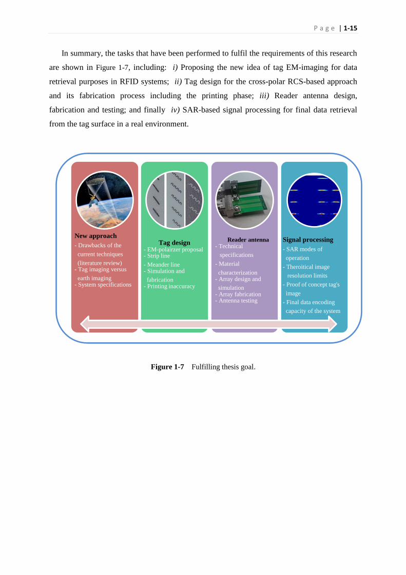
P a g e | 1-15
In summary, the tasks that have been performed to fulfil the requirements of this research
are shown in Figure 1-7, including: i) Proposing the new idea of tag EM-imaging for data
retrieval purposes in RFID systems; ii) Tag design for the cross-polar RCS-based approach
and its fabrication process including the printing phase; iii) Reader antenna design,
fabrication and testing; and finally iv) SAR-based signal processing for final data retrieval
from the tag surface in a real environment.
Figure 1-7 Fulfilling thesis goal.
New approach
- Drawbacks of the
current techniques
(literature review) - Tag imaging versus
earth imaging - System specifications
Tag design - EM-polairzer proposal - Strip line
- Meander line - Simulation and
fabrication - Printing inaccuracy
Reader antenna - Technical
specifications
- Material
characterization - Array design and
simulation - Array fabrication - Antenna testing
Signal processing
- SAR modes of
operation
- Theroitical image
resolution limits
- Proof of concept tag's
image
- Final data encoding
capacity of the system

P a g e | 1-16
1.7 Original contributions
Fulfilling the thesis goal and tasks performed have yielded the following original
contributions of the thesis:
1. Image-based mm-wave encoding for the chipless RFID system. The new encoding
scheme enhances the data encoding capacity of the chipless system suitable for many
commercial applications.
2. The new cross-RCS level working basis that is immune to multipath interferences and
ambient noises hence works better in harsh industrial environments.
3. mm-wave EM-polariser chipless tag that provides a very small tag size with high data
encoding capacity.
4. Design and optimisation of two EM-polarisers, strip line and meander lines, with
excellent performance based on the printed version of the polarisers utilising conductive
ink and paper substrate.
5. Novel tag design, based on the printed polarisers, that is chipless, fully printable, low cost,
robust, and is of high data capacity, small size and cross polarised–based.
6. A new matrix-based tag structure for a proper reading process based on the proposed
SAR theory.
7. Design, optimisation and fabrication of new array antennas with 12% bandwidth and very
high CPL that is suitable for the application of the cross-polar RCS EM-image based
chipless RFID system.
8. The proven concept of MIMO-based array antenna for fast imaging purpose.
The aforementioned original contributions, in the field of research result in: i) four referred
journal papers (one accepted and three under review), ii) 11 refereed conference papers, iii)
one Australian provisional patent application and a successful grant of US$ 90,000 from the
Xerox, USA. The full list of publications can be found on pages v to vi of this dissertation.

P a g e | 1-17
1.8 Thesis outline
The research embodied in this thesis is divided into nine chapters. Each chapter aims to
provide a smooth transition from the start of the research to its final goal.
Chapter 1 Introduction
A brief overview of the industries with identification and tracking requirements is provided
in this chapter. High data encoding capacity and low system cost are appeared as the top
priorities of the industries for identification purpose. The barcode system as a well-stablished
identification technique is then reviewed regarding its ultimate potentials for addressing the
current demands of industries. It is shown that the limitations of the barcodes on providing
enough content capacity and also their high labour costs are not compatible with the needs of
industries in the modern international trading market. The RFID system as an alternative
solution is introduced and its main limitation on providing cheap tagging solution is
presented. Conventional techniques in the chipless RFID systems are reviewed. Finally, the
mm-wave image based chipless RFID system is briefly introduced and its salient attributes
are highlighted.
Chapter 2 High data capacity, printable chipless RFID tag
The literature review related to the proposed technique of cross-polar image-based chipless
RFID systems is provided in Chapter 2. It first considers the potentials of the chipless RFID
system to fulfil the requirements of the main industries with billions of yearly tag usage. A
fully printable chipless tag structure is suggested as the only option to satisfy the tag
expectation by industries. Conventional techniques in the chipless RFID systems are
reviewed and their final capabilities based on a fully printable tag are fully investigated.
Potentials of the proposed technique, specifically regarding the tag cost and content capacity,
are introduced then.
Chapter 3 EM-imaging through reflective EM-polariser
This chapter shows the possibility of EM-imaging for data encoding purposes in the
chipless RFID tag. It first highlights the main difference between the proposed approach of
EM-imaging and other conventional techniques in RFID systems. Then the chapter is divided
into two almost separate parts. In the first part the millimetre scanning of the tag surface is
considered. Then the novel idea of a strip line and a meander line as effective polarisers are

P a g e | 1-18
introduced and the working basis of these two elements based on diffraction theory and
resonance is presented. Finally, the technical and regulatory situation of the 60 GHz band is
also covered in this section.
Chapter 4 Practical data encoding EM-polariser
The fabrication process of the proposed strip line and meander line EM-polarisers is
discussed in this chapter. Both polarisers are fabricated through two different technologies.
First, the costly but accurate approach of a photolithographic process that utilises annealed
copper and high quality substrate is considered. Then the same tags are printed through a
commercial printing process that is very cheap but includes many printing inaccuracies. Two
samples are measured in real scenario for their final performance. While precise fabricated
tags show similar results as expected by simulation, the printed version of the tags lose their
resonance behaviour though still creating high cross-polar components. Based on the printed
tag performance, then an on/off data encoding algorithm is proposed.
Chapter 5 Printed EM-polariser performance
The actual performance of the printed polariser-based tag is considered in Chapter 5. First
an analytical model of the reading scenario for the chipless RFID system is developed based
on radar theory. Based on this analytical model, the performance of co- and cross-polar RCS-
based systems are compared. Different measurement scenarios are considered for
confirmation of the analytical assumptions. The printed tags are measured against their
performance in severe multipath scenarios, tagging of highly reflective items, bending
effects, and barrier effects. Based on the successful measurement results, it is concluded that
the proposed tag structure provides a very robust, reliable and fully practical solution for the
industrial applications.
Chapter 6 Reader antenna
The reader antenna is discussed in Chapter 6. It first reviews the technical and operational
necessities of reader antennas for the image-based chipless RFID system. Then an array of
double side printed dipole (DSPD) antennas is proposed to satisfy the required technical
specifications. The substrate characterisation is performed through a substrate integrated
waveguide (SIW) resonant technique at 60 GHz. Finally the array is fabricated through
standard printed circuit board (PCB) technology and tested. The array adequately covers the

P a g e | 1-19
whole frequency range of operation 57-64 GHz. The antenna provides a uniform radiation
pattern in the azimuth direction with a limited pattern on the elevation angle. The measured
CPL is below -20 dB. The measured gain of the array is 5.5-7 dBi over the entire frequency
range of operation. The size of the array is 22 × 14 mm2.
Chapter 7 Electromagnetic imaging
This chapter briefly reviews the SAR theory. The necessity of SAR for the chipless RFID
application is shown. Then three modes of operation in SAR theory are discussed and the
suitable scenario for the chipless RFID is proposed. The range and azimuth image resolutions
are introduced and it is discussed that only azimuth resolution of few millimetre is feasible.
Then appropriate tag structure is designed for high data encoding capacity and reliable
reading process. In the final stage of this chapter, the EM-images of some sample tags with
different data encoding capacity are shown which successfully reveals the tag’s data. A tag
with 8.5 cm length encodes 17 bits of data while the tag width is only one cm. This step
fulfils the main goal of the research on proposing a new approach to data encoding algorithm
based on a fully printable tag structure.
Chapter 8 MIMO-based array antenna for fast imaging
The requirement for physical movement of the reader and tag is considered in this chapter.
The novel idea of MIMO-based system is suggested to eliminate this necessity and suggest a
very fast imaging algorithm. The theory of MIMO-based array antenna is comprehensively
introduced. The proposed approach is considered for providing a fast imaging means through
utilising only 55 physical elements .This new system structure is used in a simulation step to
provide an EM-image of the tag. The characteristics of the provided image through new
technique of MIMO-based reader are then compared with the conventional SAR technique
results.
Chapter 9 Conclusion and future works
The conclusions focus on the important findings and outcomes of this research project and
highlight the key aspects of the work. A brief review of each chapter is also discussed in
conclusion. Moreover, the proposal for enhancing the data encoding capacity through three-
level data encoding and the tag orientation sensitivity are introduced as the future work of
this research.

P a g e | 1-20
1.9 Communications of results
The outcomes of this research have been divided in the following categories:
Grant Success:
Xerox, USA, University Affairs Committee (UAC) Grant, mm-wave Chipless RFID tag,
Investigators, A/P Nemai Chandra Karmakar and Mohammad Zomorrodi, Department of
Electrical and Computer Systems Engineering, Monash University, Clayton, Australia,
Xerox, USA Investigator, Dr. Timothy Stowe, Program Manager, Xerox PARC, Inc, Palo
Alto, CA, USA, $115,865 AUD from 2015-2017
Remarks: Collaboration with Xerox Ltd, USA is based on the outcomes of this PhD research.
The grant application was ranked in the top 3 proposals among more than 20 shortlisted
applications from reputed universities from all over the world.
Journals papers:
[1] M.Zomorrodi, and N.C.Karmakar, “ A Low Cost Wideband Printed Dipole Array
Antenna for 60 GHz Image-Based Chipless RFID Reader ”, in IEEE Antennas and
Propagation Magazine, accpeted on 1st Jan 2015.
[2] M.Zomorrodi, N.C.Karmakar and J.Walker, “ Fast Imaging Technique for Chipless
RFID Tag “, submitted on 15th
Jan 2015 to IEEE Transactions on Microwave Theory
and Techniques as the extended version of IMaRC-2014 conference paper, under
review process.
[3] M.Zomorrodi, and N.C.Karmakar, “ Electromagnetic Imaging, a New Power for
Chipless RFID System”, in Cambridge Press, Submitted on Feb 2015.
[4] M.Zomorrodi, N.C.Karmakar and J.Walker, “mm-Wave Cross-Polar EM-imaging
for High Data Capacity Chipless RFID System “, to IEEE Transactions on Antennas
and Propagation, submitted on 5th June 2015.
[5] M.Zomorrodi, N.C.Karmakar and J.Walker, “Fast EM-imaging of Chipless RFID
System Through MIMO-based Technique“ to IEEE Transactions on Microwave
Theory and Techniques as the extended version of IMS-2015 conference paper.
submitted on 24th June 2015.

P a g e | 1-21
Conference papers:
[1] M.Zomorrodi, “Improved Genetic Algorithm Approach for Phased Array Radar Design”, in
Asia-Pacific Microwave Conference, APMC, Melbourne, Australia, 2011.
[2] M. Zomorrodi and N.C.Karmakar, “60 GHz Dipole Array Antenna for SAR-based Chipless
RFID”, in 13th Australian Symposium on Antennas, Sydney, 2013.
[3] M.Zomorrodi, N.C.Karmakar, and S.G.Bansal, “Introduction of Electromagnetic Image-
based Chipless RFID System,” in Intelligent Sensors, Sensor Networks and Information
Processing (ISSNIP-2013), Melbourne, 2013, pp. 443-448.
[4] M.Zomorrodi and N.C.Karmakar, “Cross-RCS Based, High Data Capacity, Chipless RFID
System”, in International Microwace Symposium (IMS-2014), Tampa Bay, Flordia, US,
2014.
[5] M.Zomorrodi and N.C.Karmakar, “An Array of Printed Dipoles at 60 GHz”, in IEEE
International Symposium on Antennas and Propagation, Memphis, Tennessee, USA, July-
2014, pp. 73-74.
[6] M.Zomorrodi and N.C.Karmakar, “On the Usage of Diffraction effect for Chipless RFID
Systems”, in Australian Microwave Symposium (AMS), Melbourne, Australia, June 2014.
[7] M.Zomorrodi and N.C.Karmakar, “Cross-Polarized Printable Chipless RFID Tag with
Superior Data Capacity”, in European microwave week, EuMW2014, Rome, Italy, 2014.
[8] M.Zomorrodi and N.Karmakar, “Image-based Chipless RFID System with High Content
Capacity for Low Cost Tagging”, in International Microwave and RF Conference (IMaRC)
Bangalore, India., 2014.
[9] M. Zomorrodi and N.C.Karmakar, “ Fabrication Error Tolerant Array Antenna at 60 GHz”,
in 14th Australian Symposium on Antennas, Sydney, Feb-2015.
[10] M.Zomorrodi and N.C.Karmakar, “ Novel MIMO-based Technique for EM-imaging of
Chipless RFID, ” in International Microwace Symposium (IMS- 2015), Phoenix, USA,
May-2015.
[11] M.Zomorrodi and N.C.Karmakar, “On the Study of Fabrication Errors on mm-Wave
Antenna”, in IEEE International Symposium on Antennas and Propagation, Vancouver, BC,
Canada, July-2015.

P a g e | 1-22
Patent:
M.Zomorrodi, N.Karmakar, “MM-Wave Image-based chipless RFID system”, Australia
provisional patent, Dec 2013, Patent number: 2013-071.
Book Proposal:
Karmakar, Nemai; Zomorrodi, Mohammad; Divarathne, Chamath, “Advanced Signal
Processing Techniques for Chipless RFID Systems”, John Wiley & Sons, Inc. (Submitted on
September 2014 and approved by Wiley on 3rd
July 2015)
Project Awards and Achievements:
Second place in 3 minutes thesis competition (3MT) at the Postgraduate Research
Forum, Monash University, July 2012.
Second place in poster competition at the Postgraduate Research Forum, Monash
University, July 2012.
Recipient of the Post publication Award (PPA), Monash University 2015.

P a g e | 2-23
Chapter 2 High data capacity, printable chipless RFID tag
2.1 Introduction
Identification systems were introduced in Chapter 1, and the reasons why barcodes are
unable to satisfy the current requirements of main stream industries was described. Chipped
RFID systems were considered as an alternative approach to barcodes. It was shown that they
are not able to meet the requirements of main stream applications due to their higher tag cost.
Then chipless RFID systems were considered as a solution for low cost item tagging.
However, the developed and reported chipless RFID tags have limitations in terms of number
of data bits, costs, reading methods and collision avoidance in multiple tag reading scenarios.
As a solution to some of these limitations, high data capacity mm-wave chipless RFID tag is
proposed. Finally, the basics of the proposed cross polar-RCS based approach were presented,
together with some of its potential advantages with respect to other chipless techniques.
This chapter focuses on the importance of a printable tag solution for chipless RFID
systems. It discusses how the main stream application of identification systems will be
satisfied with a printable tag solution alone, at less than one cent (1¢) final tag cost. A review
of the current techniques in chipless RFID systems is provided, and their final data encoding
capacity based on the printable version of their proposed tag structures is considered. The
idea of EM-imaging for data encoding in a chipless tag is also presented along with a review
of EM-imaging in other applications. Finally, it is shown that the imaging is applicable to
chipless RFID systems, and that it has potential to enhance the capabilities of current
techniques in the chipped or chipless RFID systems.
2.2 Tag price sensitivity versus applications
Tough trading conditions due to global competition means that organisations and
companies need to attain more process efficiencies. This would enable them to drive down
their product costs and provide competitive advantages. Just-in-time retailing was introduced
as an effective model for many organisations instead of traditional logistic procedures.
Although retailers benefit from lower stock levels through new management systems, more
pressure is experienced by manufacturers and distributors to address the retailers’
requirements in a shorter time frame. Effective goods tracking systems are then required to
assist the implementation of the new management systems through the supply chain [41].
Barcodes, as a well-established identification system, are unable to address the new

P a g e | 2-24
requirements due to their technical limitations. The requirements for line-of-sight reading and
the non-flexible automatic reading scheme of barcodes drive up tracking cost due to labour
intervention. Moreover, its limited data capacity, as discussed in Chapter 1, limits the new
supply chain environment. For example, Walmart has mandated RFID technology for their
thousands of manufacturers for goods flow visibility from manufacturer to the crashing point
of boxes when the goods are sold [42].
RFID systems are an emerging tracking system with many advantages over barcodes. They
have appealed to many organisations as an effective identification means for fulfilling the
requirements of the modern supply chain. Unlike barcodes, RFID tags are robust and do not
need a line-of-sight reading scenario, hence removing the need for labour intervention. RFID
tags are also capable of carrying information about the location, destination, and product
identification number as their data encoding capacity is much higher than that of barcodes.
However, the price of these RFID tags remain as the first and foremost hurdle for their
deployment in applications with low product costs; groceries for example. As discussed in
Chapter 1 (1.1), the identification system cost linearly depends on the tag cost for large
quantity tagging requirements. Based on the company’s potential and system affordability,
the relation between the tag cost and its volume is shown in Figure 2-1 [1]. Based on this
model the RFID tag cost would be a large barrier in organisations with a high tagging
requirements. As shown in Figure 2-1, the chipless tags are necessary to satisfy the
requirements of medium to large-sized organisations, with a tag price to be down to 1¢.
Although the chipless tags eliminate the need for the silicon chip, as the most expensive
element of the tag structure, there are other factors which may surge the tag cost. The tag
fabrication technique and its possible requirements to other elements rather the silicon chip
along with heir installation process may elevate the tag cost higher than the targeted value of
1¢. Therefore, based on the worldwide well accepted model shown in Figure 2-1, the main
stream industries with billions of yearly tag requirements will only be satisfied through a
fully printable chipless tag structure. Any technique or suggested solution for a chipless
RFID system, must consider this critical point of the industries for a printed tag, otherwise
the proposed technique finds no place in the identification market or at least in main stream
industries.
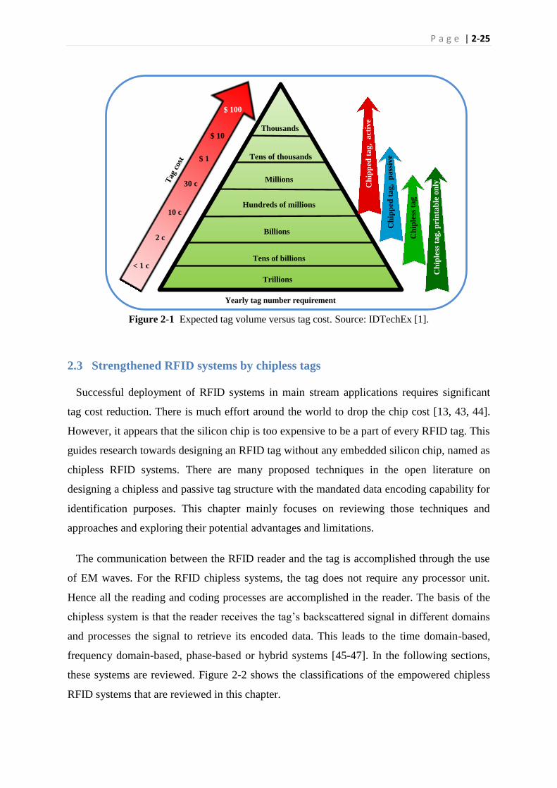
P a g e | 2-25
Figure 2-1 Expected tag volume versus tag cost. Source: IDTechEx [1].
2.3 Strengthened RFID systems by chipless tags
Successful deployment of RFID systems in main stream applications requires significant
tag cost reduction. There is much effort around the world to drop the chip cost [13, 43, 44].
However, it appears that the silicon chip is too expensive to be a part of every RFID tag. This
guides research towards designing an RFID tag without any embedded silicon chip, named as
chipless RFID systems. There are many proposed techniques in the open literature on
designing a chipless and passive tag structure with the mandated data encoding capability for
identification purposes. This chapter mainly focuses on reviewing those techniques and
approaches and exploring their potential advantages and limitations.
The communication between the RFID reader and the tag is accomplished through the use
of EM waves. For the RFID chipless systems, the tag does not require any processor unit.
Hence all the reading and coding processes are accomplished in the reader. The basis of the
chipless system is that the reader receives the tag’s backscattered signal in different domains
and processes the signal to retrieve its encoded data. This leads to the time domain-based,
frequency domain-based, phase-based or hybrid systems [45-47]. In the following sections,
these systems are reviewed. Figure 2-2 shows the classifications of the empowered chipless
RFID systems that are reviewed in this chapter.
Trillions
Tens of billions
Billions
Hundreds of millions
Millions
Tens of thousands
Thousands
Ch
ipp
ed t
ag,
act
ive
Ch
ipp
ed t
ag, p
ass
ive
Ch
iple
ss t
ag
Ch
iple
ss t
ag,
pri
nta
ble
on
ly
Yearly tag number requirement
Tag
cos
t
$ 100
$ 10
$ 1
30 c
10 c
2 c
< 1 c
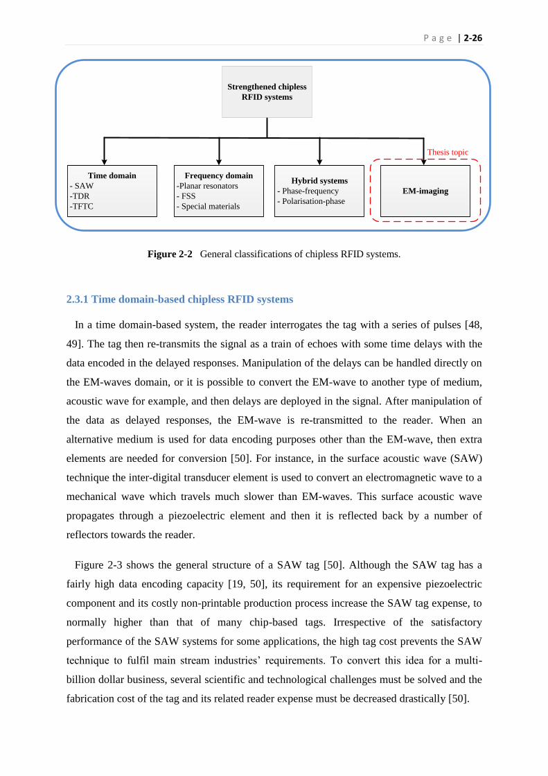
P a g e | 2-26
Figure 2-2 General classifications of chipless RFID systems.
2.3.1 Time domain-based chipless RFID systems
In a time domain-based system, the reader interrogates the tag with a series of pulses [48,
49]. The tag then re-transmits the signal as a train of echoes with some time delays with the
data encoded in the delayed responses. Manipulation of the delays can be handled directly on
the EM-waves domain, or it is possible to convert the EM-wave to another type of medium,
acoustic wave for example, and then delays are deployed in the signal. After manipulation of
the data as delayed responses, the EM-wave is re-transmitted to the reader. When an
alternative medium is used for data encoding purposes other than the EM-wave, then extra
elements are needed for conversion [50]. For instance, in the surface acoustic wave (SAW)
technique the inter-digital transducer element is used to convert an electromagnetic wave to a
mechanical wave which travels much slower than EM-waves. This surface acoustic wave
propagates through a piezoelectric element and then it is reflected back by a number of
reflectors towards the reader.
Figure 2-3 shows the general structure of a SAW tag [50]. Although the SAW tag has a
fairly high data encoding capacity [19, 50], its requirement for an expensive piezoelectric
component and its costly non-printable production process increase the SAW tag expense, to
normally higher than that of many chip-based tags. Irrespective of the satisfactory
performance of the SAW systems for some applications, the high tag cost prevents the SAW
technique to fulfil main stream industries’ requirements. To convert this idea for a multi-
billion dollar business, several scientific and technological challenges must be solved and the
fabrication cost of the tag and its related reader expense must be decreased drastically [50].
Strengthened chipless
RFID systems
Time domain
- SAW
-TDR
-TFTC
Frequency domain
-Planar resonators
- FSS
- Special materials
Hybrid systems
- Phase-frequency
- Polarisation-phase
EM-imaging
Thesis topic
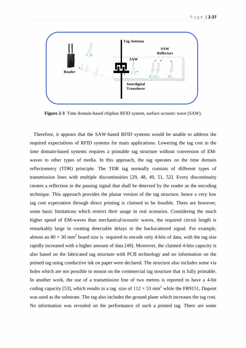
P a g e | 2-27
EFI
SAW
Reflectors
Tag Antenna
Interdigital
Transducer
Reader
SAW
Figure 2-3 Time domain-based chipless RFID system, surface acoustic wave (SAW).
Therefore, it appears that the SAW-based RFID systems would be unable to address the
required expectations of RFID systems for main applications. Lowering the tag cost in the
time domain-based systems requires a printable tag structure without conversion of EM-
waves to other types of media. In this approach, the tag operates on the time domain
reflectometry (TDR) principle. The TDR tag normally consists of different types of
transmission lines with multiple discontinuities [29, 48, 49, 51, 52]. Every discontinuity
creates a reflection in the passing signal that shall be detected by the reader as the encoding
technique. This approach provides the planar version of the tag structure, hence a very low
tag cost expectation through direct printing is claimed to be feasible. There are however,
some basic limitations which restrict their usage in real scenarios. Considering the much
higher speed of EM-waves than mechanical/acoustic waves, the required circuit length is
remarkably large in creating detectable delays in the backscattered signal. For example,
almost an 80 × 30 mm2 board size is required to encode only 4-bits of data, with the tag size
rapidly increased with a higher amount of data [49]. Moreover, the claimed 4-bits capacity is
also based on the fabricated tag structure with PCB technology and no information on the
printed tag using conductive ink on paper were declared. The structure also includes some via
holes which are not possible to mount on the commercial tag structure that is fully printable.
In another work, the use of a transmission line of two metres is reported to have a 4-bit
coding capacity [53], which results in a tag size of 112 × 53 mm2 while the FR9151, Dupont
was used as the substrate. The tag also includes the ground plane which increases the tag cost.
No information was revealed on the performance of such a printed tag. There are some
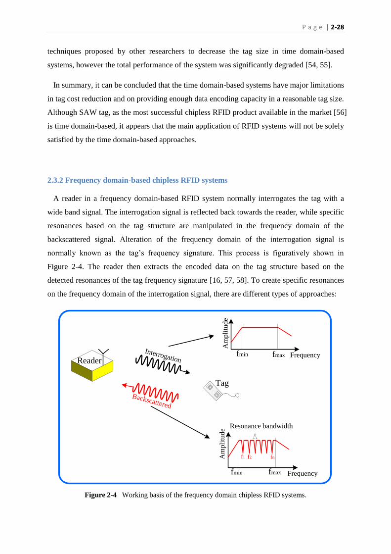
P a g e | 2-28
techniques proposed by other researchers to decrease the tag size in time domain-based
systems, however the total performance of the system was significantly degraded [54, 55].
In summary, it can be concluded that the time domain-based systems have major limitations
in tag cost reduction and on providing enough data encoding capacity in a reasonable tag size.
Although SAW tag, as the most successful chipless RFID product available in the market [56]
is time domain-based, it appears that the main application of RFID systems will not be solely
satisfied by the time domain-based approaches.
2.3.2 Frequency domain-based chipless RFID systems
A reader in a frequency domain-based RFID system normally interrogates the tag with a
wide band signal. The interrogation signal is reflected back towards the reader, while specific
resonances based on the tag structure are manipulated in the frequency domain of the
backscattered signal. Alteration of the frequency domain of the interrogation signal is
normally known as the tag’s frequency signature. This process is figuratively shown in
Figure 2-4. The reader then extracts the encoded data on the tag structure based on the
detected resonances of the tag frequency signature [16, 57, 58]. To create specific resonances
on the frequency domain of the interrogation signal, there are different types of approaches:
Figure 2-4 Working basis of the frequency domain chipless RFID systems.
Reader
Interrogation
Backscattered
Tag
fmin Frequency
Am
pli
tude
fmax
Frequency
Am
pli
tude
f1 f2 fn
Resonance bandwidth
fmin fmax

P a g e | 2-29
i. Planar structure resonators [16]
ii. Frequency-selective surface (FSS) based resonators [59, 60], and
iii. Special materials usage for resonant purposes [20, 21, 61-64].
2.3.2.1 Planar structure resonators
Jalaly et al. [65] proposed some RF barcode type structures for data encoding. The structure
is composed of planar dipoles, similar to barcodes that resonate at different frequency bands.
To enhance the content capacity of the tag, it was proposed to use all available industrial,
scientific and medical (ISM) radio frequency bands. Based on the proposal, every ISM band
is capable of encoding a maximum of five bits. This expectation is based on simulation
results. The precisely fabricated tag on the Taconic-TLY (ɛr = 2.2) substrate creates
detectable resonances. However, based on the simulation results, the occurred resonances
have 4 to 6 dB resonance deep that would be difficult for detection purposes in real scenario.
It is very obvious that the same structure is not capable of creating detectable resonances if
the tag is printed on a lossy paper substrate with low conductive ink. Moreover, system
reliability decreases when multipath and clutter interferences are considered. The effect of
printing inaccuracy on the length of the dipoles, which creates a resonance shift, is also
another factor which affects the consistency of the system performance.
Microstrip spiral resonators were proposed to create sharp resonances on the frequency
domain of the backscattered signal [16]. The chipless tag also comprises a cross-polarised
transmitting and receiving microstrip ultra-wideband (UWB) disc loaded monopole antenna.
It was shown that the system is capable of encoding up to 35 bits at 4 GHz frequency
bandwidth. This is a significant success in the content capacity of the chipless RFID systems.
However, certain circumstances were considered for the measured data capacity. First, the tag
was fabricated through a costly process using PCB technology on the low loss material of
Taconic TLX-0 (ɛr = 2.45). Moreover, the printed tag with conductive ink on a paper base
will experience significant Q-factor drop due to the printing errors, high loss of the paper and
low conductivity of the ink. These factors may limit the actual data encoding capacity of the
proposed structure. However, the proposed idea in this work suggests a wide range of
potentials for chipless RFID systems.

P a g e | 2-30
Fractal structures, as the load section of a wideband monopole antenna with encoding
capability, were proposed by Balbin [66]. Based on the type and length of the fractal
structures, multiple resonances would be detectable in the backscattered signal. However, due
to the complex coupling behaviour among the branches of a fractal structure, the resonance
frequencies alteration seems to be unpredictable. This may restrict the actual usage of the
fractal structure for the RFID applications. Moreover, in the proposed work, the behaviour of
precise fabricated structures was only considered and there was no study on the printable
version of the fractal resonators. Considering the very tiny and complex shape of fractal
structures, it is suggested that printing issue may cause more complexity on the frequency
resonances of the tag. No further results have been reported on the fractal resonators for the
RFID applications.
Using split ring resonators (SRRs) was also proposed for the data encoding purposes on the
chipless RFID systems [67]. The proposed tag structure was printed on the poly carbonate
(ɛr = 3.25) material and measured on the frequency range 8-12 GHz. The tag was capable of
encoding four bits of data on a 4 GHz spectrum bandwidth. The authors suggested using
waveguide antennas to create a small illumination zone. By repeating the split ring resonators
on the tag surface, more encoding capacity would be feasible. The proposed technique would
be suitable for security of credit/personnel cards. However, due to the low encoding capacity
the proposed approach is not practical for identification purposes.
As an advanced approach, the usage of complex natural resonances was proposed to
enhance the content capacity of a chipless RFID system [30]. Based on the singularity
expansion method (SEM), complex natural resonances are aspect-independent parameters
which include some structural information of the scattering target. This technique suggests
encoding of up to 24 bits in a small area of 24 × 24 mm2 that would be an extensive encoding
enhancement compared with other available approaches in the chipless RFID systems.
However, the system requires complex signal processing as multiple switching between time
and frequency domain are required to decode the tag’s content. Moreover, the performance of
the printed tag was not shown in the proposed communication. The limited conductivity of
the conductive ink and high loss tangent of the paper significantly changes the poles’
positions of the tag responses, hence the proposed data encoding scheme is challenged.
Additionally, the tag structure is very tolerance dependent as it comprises the line width and
gaps in sub-millimeter (0.2~0.7 mm). This precise structure cannot be manipulated
successfully through commercial printing facilities for low cost tag production purposes. The
P a g e | 2-31
effect of printing inaccuracy was not also considered in the proposed approach. However, the
SEM approach opens a new area of research for chipless RFID systems and may be
combined with other conventional techniques for enhancing their potentials for massive
commercialisation.
2.3.2.2 Frequency-selective surface based resonators
Frequency selective surfaces (FSSs) are constructed as the rows and columns of a particular
resonant structure designed to perform a (or a combination of) lowpass, bandpass, highpass
and bandstop filtering functions on the incident plane wave passing through, in a
measurement known as ‘transmittance’ [65, 68]. Although, barcodes and RFID systems are
reflection–based structures, sometimes the FSS are used for creating resonances in the
reflection direction and hence are suitable for RFID applications.
Costa et al. [59] proposed the usage of high-impedance surface-based multi-resonators. The
structure is based on a finite metallic FSS comprising of several concentric square loop
resonators. The reported tag structure occupies 45 × 45 mm2 area and is capable of encoding
five bits of data content. Therefore, the data encoding density is 0.25 bit/cm2 that is very low
considering the requirements of the main RFID applications. The tags are readable from 55
cm distance with zero dBm transmit power. The system had a good performance for different
tag orientation scenarios. However, the system needs a calibration measurement process for
proper reading to cancel out the effect of multipath interference and the effect of antennas;
otherwise the system fails to read and detect the tag’s data. Moreover, all measured data in
the published work is based on the fabricated tag structure with PCB standards on a FR4
substrate. No result based on the printed tag structure was revealed.
In another work a stacked multilayer patch antennas is used as an all-pass network to
provide more robustness with respect to multipath and clutter interferences [60]. In the
proposed theory, instead of relying on an amplitude-frequency response of the multilayer
structure, the phase-frequency response is considered. A three-layer structure with 18 × 18
mm2 area is able to decode two bits of data content based on the simulation results. No
measurement of the proposed tag structure was shown in that communication. However, the
performance of the proposed structure is directly linked to the conductivity and loss tangent
of the substrate. This suggests that the fabricated and printed tag may show significant
performance degradation with respect to the simulation result. Moreover, printing of a three-
P a g e | 2-32
layer structure increases the tag fabrication cost and may not meet the low cost expectation of
the RFID tag for the main industries.
2.3.2.3 Material-based resonators
CorssID [61], a telecommunication company, has reported developing a chipless RFID
system that provides a reliable authentic approach for valuable documents, such as
intelligence agency reports, financial securities and banknotes. The system uses "nanometric"
materials, tiny particles of chemicals with varying degrees of magnetism, that resonate when
bombarded with electromagnetic waves from a reader. Each chemical emits its own distinct
radio frequency, or “note”, that is picked up by the reader, and all the notes emitted by a
specific mix of different chemicals are then interpreted as a binary number. Since the system
uses up to 70 different chemicals, each chemical is assigned its own position in a 70-digit
binary number [61]. No further information about the working prototype and its applicable
tag cost have been released since it was introduced in 2004.
In 2007 Somark Innovation declared that it has a special readable ink as a chipless RFID
tag that can be used to track animals, cattle for example, or even human beings. No further
discussion is disclosed by the company and no information is also available on its encoding
capacity or the ink (tag) cost [62, 63].
A fair comparison among different chipless RFID system techniques with or without meta-
materials are provided by Mandel et al. [20]. In this communication, various approaches were
studied in terms of their merits, frequency band usage, and tag size for one bit of content,
then they concluded that the meta-materials can shrink the tag size hence enhancing the
merits of the structure. Although in their study, the time and frequency based systems were
considered with the application of meta-materials, no information about the tag cost utilizing
meta-materials was provided.
2.3.3 Phase-domain based and hybrid chipless RFID systems
Phase-domain based system is proposed as a method of data encoding to rely on the phase
information of the backscattered signal. In one proposal, the tag consists of some plurality of
antenna elements with different dimensions and orientations that provide polarisation and

P a g e | 2-33
phase information [69]. The interrogator device scans the area and uses radar imaging
techniques to create an image of the scanned scene. The re-radiated RF signals of the tag
preferably include polarisation and phase information of each antenna element. The proposed
tag shapes are presented in Figure 2-5 with dipoles of different length and width. Four
different orientations are suggested for each antenna size at angles 0°, +/- 45°, and 90°, which
control their particular phase and polarisation responses. It has been also proposed to use
some reflective rectangles with two (or more) reactive stub loading which are extended from
rectangle antennas. One is perpendicular to the antenna and the other is parallel to the antenna
polarisation. In this case, the length and position of the reactive stub elements control the
phase and polarisation parameters of the reflected signal respectively. It is claimed that the
proposed system has the ability to read and track chipless tags from 100 m away and to read
thousands of tags per second [1, 69]. However, no commercial product is available on the
market based on this approach yet. This is probably because the content encoding in RFID
systems through phase and polarisation is very expensive and sometimes impractical. The
phase of the reflection by a given element is dependent on its distance to the reader. This
means that a slight bending of the tag surface causes a significant phase shift specifically in
higher frequencies. There are suggestions to mitigate the phase ambiguity, however the
solutions only apply to chipped-tags for low frequencies, below 1 GHz, and no work is
reported on chipless systems [70, 71].
Bow-tie dipole elements
Rectangular reactively-loaded patch
Figure 2-5 Phase-domain based chipless RFID tags.

P a g e | 2-34
As a hybrid based system, the combination of phase deviation and frequency position of the
resonances was proposed as the data encoding approach in a chipless RFID system [72]. The
tag consists of multiple “C” shaped resonators which are interrogated through a wideband
signal in the band 2.5-7.5 GHz. The claimed content encoding capacity is 23 bits with five “C”
shape resonators. The encoding is based on a matrix of frequency and phase shift deviation.
However, the tag was tested in the anechoic chamber and no further discussion was
communicated to explore the effect of multipath interference on the system performance.
This would be an important aspect of the proposed approach as the reflection from other
objects will cause significant effects on the phase shift. There is a need for pre-measurement
of the scene to calibrate the system as well. This means that the system is vulnerable to errors
if any changes happen in the surrounding area of the tag. Moreover, the performance of the
tag is not clear regarding to the bending effect. The performance of a real printed tag
structure was also not discussed.
In another work, the amplitude and frequency-based encoding scheme is proposed as a new
encoding approach for enhancing the content capacity of the chipless RFID systems [73]. The
split ring resonator (SRR) is the proposed resonator type, and based on the received signal
level and the position of the resonances, the data can be encoded. Although system content
capacity is increased, the system complexity and also its sensitive performance towards noise
and multipath interference may prevent its actual usage.
2.4 EM-imaging in various applications
Carl A. Wiley, a mathematician at Goodyear Aircraft Company in Litchfield Park, Arizona,
invented synthetic-aperture radar (SAR) in June 1951 while working on a correlation
guidance system for the Atlas IBM program [74]. Nowadays, electromagnetic imagery based
on SAR theory is of widespread interest and is extensively used in military and civil
applications. In the SAR-based system, a large synthetic aperture antenna is formed by a
moving antenna over the target region. The target is repeatedly illuminated with radio waves
pulses at different frequencies, and the echo waveforms received successively at the different
antenna positions are coherently detected and stored, and then post-processed together to
resolve elements in an image of the target region. The obtained EM-image of the target scene
through SAR technique acquires much finer spatial resolution than is possible with

P a g e | 2-35
conventional beam-scanning means. For applications like earth imaging, the SAR technique
is the only option as carrying a large antenna over the earth is not practical. There are
however other applications on which the usage of large antennas is feasible for imaging
purposes, but the SAR technique is preferred for different reasons. For instance, in the body
imaging application, it is possible to use a large antenna providing a high resolution EM-
image of the body; however the SAR technique is much preferred as it minimises the amount
of radiation on the body. Most body imaging systems nowadays use the SAR-based technique
to comply with EM-radiation regulations [75-77]. Through-to-wall imaging (TWI) based on
the SAR technique is also extensively used in construction activities [78] as well as
intelligence and security applications.
2.5 Potential advantages of the proposed tag structure
The literature review and analysis shows that the identification market in main stream
applications with billions of yearly tag requirements still requires an RFID product whose
technical specifications are adequately matched with industry expectations mainly on:
i. Tag cost of below one cent,
ii. Enough data content capacity in a reasonable tag size,
iii. Consistent performance based on the printed tag structure, and
iv. Reliable performance in an industrial environment.
It appears that the proposed technique of the cross-polar image-based chipless RFID system
promisingly addresses the aforementioned technical requirements and hence is capable of
significantly influencing the RFID market. The key potential advantages of the proposed tag
are as follows:
i. Printing and cost issue. The tag structure in the proposed technique utilises a tiny
conductive component which acts as effective EM-polariser. The tag is fully printable
through a low cost inkjet printer and the cost of the required ink is lower than that of a
barcode for the same content capacity as will be shown in Chapter 3 (3.3.2). All the
measurements and results in this dissertation are based on the printed tag structure
which provides satisfactory performance for the proposed system in its commercial
phase. Hence, it can be concluded that the tag cost in the proposed technique meets
industry criteria as it is less expensive than a barcode.

P a g e | 2-36
ii. High content capacity. As briefly addressed in Chapter 1, the data content capacity of
the proposed EM-imaging approach depends on the available frequency band and the
system complexity. For a fairly simple reader structure and limited bandwidth, the tag’s
encoding capacity is proportional to the tag’s length, see Figure 2-6. However, even
based on the simplicity assumptions, the proved data encoding capacity through EM-
imaging in a small tag size is much higher than of shown by other techniques to date for
a printed tag. Normally, five vertical polarisers are assumed on every vertical slice of
the tag surface, to yield a reading range of 10-30 cm. These five polarisers provide
approximately five times larger RCS than that of a single polariser. Based on this
assumption, the width of the tag is fixed at almost 10 mm. On the other hand, every 2
mm of the tag length has the potential to encode one bit of data, Figure 2-6. Hence the
data encoding capacity is one bit per 0.2 cm2 or equivalently 5 bits/cm
2. This is a
revolutionary improvement in the content capacity of the chipless RFID systems based
on a fully printable tag [1, 47]. The credit card size, 55 × 85 mm2, as discussed before is
considered as the maximum acceptable size of any RFID tag for main stream
applications. The ultimate goal of the chipless RFID systems is to reach 35~50 bits
content capacity [11, 47]. As results at the end of this thesis show, the proposed theory
of cross-polar image-based chipless system provides 17 bits of data in a strip of
8.5 × 1 cm2 that is 5.5 times narrower than a credit card size. Therefore, the content
capacity of 93 bits is easily feasible for the credit card size tag surface.
iii. Mitigation of the printing errors and performance. Many proposed chipless RFID
systems fail to address industry requirements because of the anomalies that occur during
the printing of the tag fabrication. As discussed earlier, the printed tag structure
generally suffers from two major limitations. First, the lossy characteristics of the paper
and low conductivity of the ink adversely affect the Q factor of the resonances, hence
the encoding capacity significantly reduces [79]. Second, the random anomalies
occurring during the printing process, create noticeable frequency shifts and other
unexpected effects on the tag responses, hence no reliable reading process is feasible.
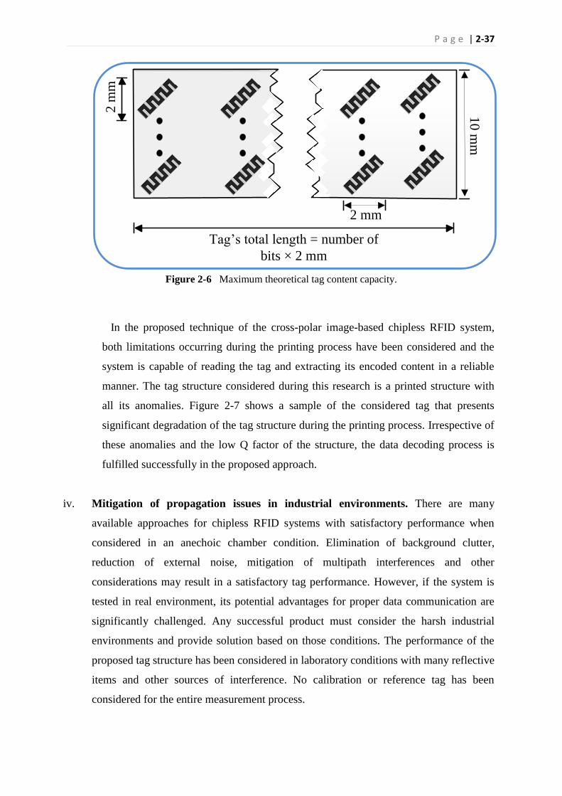
P a g e | 2-37
Figure 2-6 Maximum theoretical tag content capacity.
In the proposed technique of the cross-polar image-based chipless RFID system,
both limitations occurring during the printing process have been considered and the
system is capable of reading the tag and extracting its encoded content in a reliable
manner. The tag structure considered during this research is a printed structure with
all its anomalies. Figure 2-7 shows a sample of the considered tag that presents
significant degradation of the tag structure during the printing process. Irrespective of
these anomalies and the low Q factor of the structure, the data decoding process is
fulfilled successfully in the proposed approach.
iv. Mitigation of propagation issues in industrial environments. There are many
available approaches for chipless RFID systems with satisfactory performance when
considered in an anechoic chamber condition. Elimination of background clutter,
reduction of external noise, mitigation of multipath interferences and other
considerations may result in a satisfactory tag performance. However, if the system is
tested in real environment, its potential advantages for proper data communication are
significantly challenged. Any successful product must consider the harsh industrial
environments and provide solution based on those conditions. The performance of the
proposed tag structure has been considered in laboratory conditions with many reflective
items and other sources of interference. No calibration or reference tag has been
considered for the entire measurement process.
2 mm
10
mm
Tag’s total length = number of
bits × 2 mm
2 m
m

P a g e | 2-38
Figure 2-7 Printed tag with structural anomalies.
Moreover, the performance of the tag has also been tested for tagging of highly reflective
items, for instance aluminium can. The bending effect of the tag was also considered in the
proposed theory of the image-based system and reliable performance was experienced. The
measurement set up for different scenarios is shown in Figure 2-8.
From the above attributes of the proposed chipless RFID tag, it is inferred that the EM-
image based mm-wave tag not only mitigates many limitations of other reported chipless
RFID tags but all surpassed many propagation issues of chipped RFID tags. Therefore, the
proposed tag will become a potential identification technology for future industrial
applications.
2.6 Potential advantages of the reader system
In chipless RFID systems, the reader is required to accomplish all the data processing tasks
as the tag is a fully passive structure with no signal processing capabilities. This may increase
the complexity, cost and realisation of the reader system beyond a practical point. In the
proposed technique of the cross-polar image-based chipless RFID system, the reader is fairly
simple considering its required sophisticated reading process. The main advantages of the
proposed reader system can be summarised as:
Printed tag with meander line polariser
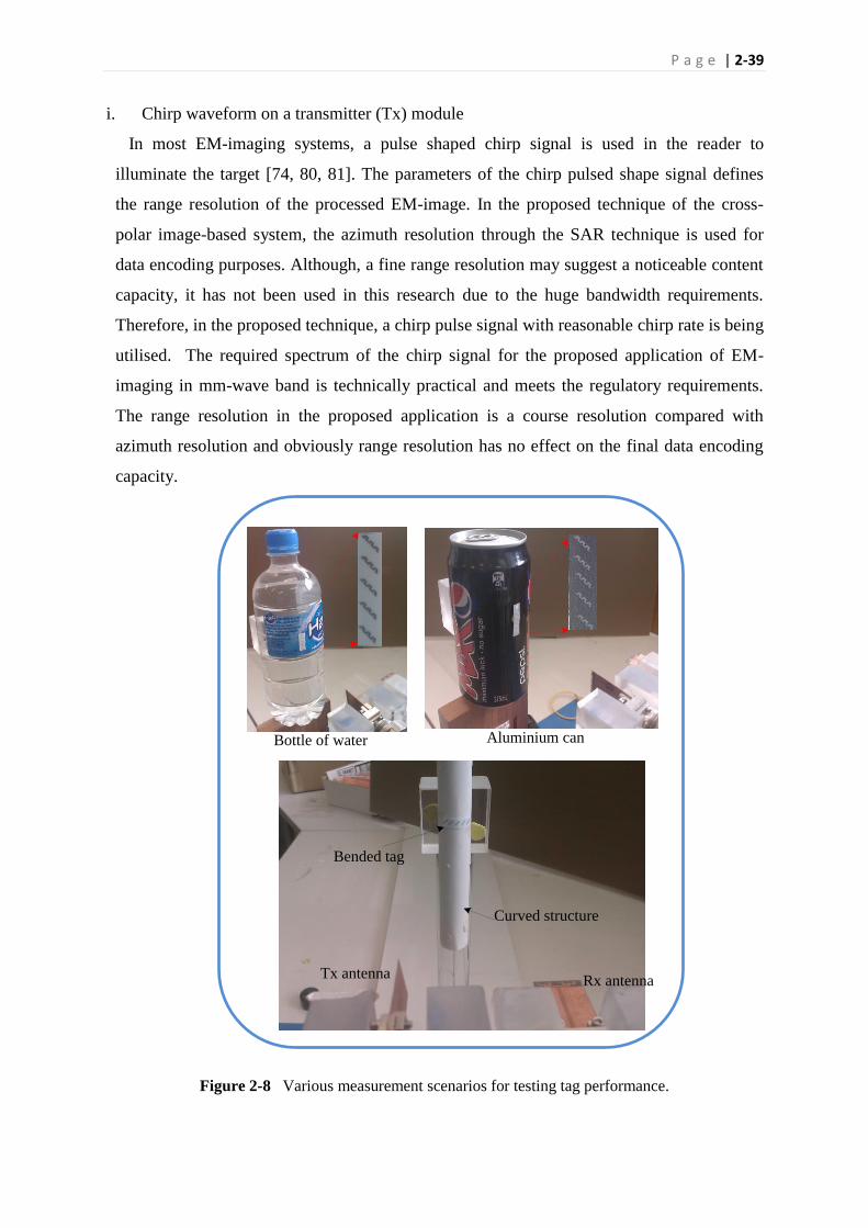
P a g e | 2-39
i. Chirp waveform on a transmitter (Tx) module
In most EM-imaging systems, a pulse shaped chirp signal is used in the reader to
illuminate the target [74, 80, 81]. The parameters of the chirp pulsed shape signal defines
the range resolution of the processed EM-image. In the proposed technique of the cross-
polar image-based system, the azimuth resolution through the SAR technique is used for
data encoding purposes. Although, a fine range resolution may suggest a noticeable content
capacity, it has not been used in this research due to the huge bandwidth requirements.
Therefore, in the proposed technique, a chirp pulse signal with reasonable chirp rate is being
utilised. The required spectrum of the chirp signal for the proposed application of EM-
imaging in mm-wave band is technically practical and meets the regulatory requirements.
The range resolution in the proposed application is a course resolution compared with
azimuth resolution and obviously range resolution has no effect on the final data encoding
capacity.
Figure 2-8 Various measurement scenarios for testing tag performance.
Aluminium canBottle of water
Tx antennaRx antenna
Curved structure
Bended tag

P a g e | 2-40
ii. Low profile, light weight and cheap antenna structure
The reader antennas for the reader side are fully planar structures that are printed on the
Taconic TLX-8 substrate through the normal PCB fabrication process. Each antenna is an
array of four double side printed dipoles (DSPD) on which the total size of the array is
1.5 × 2.5 cm2 including its feedline. The antenna performance is suitably tailored for the
proposed application, specifically its CPL and radiation patterns. The light weight and small
size of the antenna structure is also very convenient for the physical movement of the array
as required for creation of a synthetic aperture around the tag. However, appropriate
suggestions are provided to eliminate the physical movement of the antenna and increase
the reading time. Example includes the MIMO-based array antenna concept proposed at the
end of this dissertation for fast imaging purpose [82].
iii. No requirement for calibration
In the proposed approach of the cross-polar image-based system, deletion of the
background clutter is not required as those interferences are in a co-polar direction while the
system is cross polar-based. Moreover, no reference tag is utilised for calibration of the
reading process. These factors facilitate the reading process and simplify the reader system.
iv. High robustness toward interference
The system shows high robustness towards any interference coming from objects around
the tag, which result in fewer constraints on the reader system. The reader’s antennas are not
required to create nulls in any direction for minimisation of interference, hence benefiting
freedom on their radiation patterns. Moreover, no extra signal processing is necessary on the
reader side to cancel the interferences.
From the above discussion on the proposed tag and reader architecture, it is evident that an
EM-image based chipless RFID system is implementable in commercial domain. Although, it
is perceived that 60 GHz transceiver modules, switching elements and antennas are too
expensive for commercial applications, the advent of 60 GHz modules [83], switches [84],
the developed antenna [85], and in-house developed signal processing algorithm proves the
commercial potentials of the proposed system.
P a g e | 2-41
2.7 Conclusion
This chapter has identified the requirements of industry for main stream applications and
reviewed the tag cost, content capacity and other specifications, showing that billions of
yearly tag consumptions would only be financially feasible if the tag price should drop to
below one cent. The chipped tag was considered from a cost perspective and shown to be too
expensive due to the silicon chip requirement. Consequently a chipless tag was considered
the only RFID product with potential to address the cost requirements of industry.
Time-domain based chipless RFID systems, e.g SAW tags, were identified as the most
successful product available in the market to date. However, products with high encoding
capacity using this technique are too expensive, and cheap solutions suffer from very low
data encoding capacity within a reasonable and practical tag size. Frequency domain-based
chipless RFID systems provide an enhancement of the data encoding capacity of the chipless
RFID systems based on the laboratory condition. However, their performance significantly
drops when a printed tag structure is tested. This is due to the low Q factor of the printed
resonators through using conductive ink on paper. Moreover, printing inaccuracy results in a
frequency shift that reduces the reliability of the reading process. Other hybrid systems were
also briefly reviewed. Phase domain-based systems suffer from very complex reader
architecture, while the system performance is very sensitive with respect to a minor change in
the tag structure or surrounding area.
Due to the limitations of the current techniques in chipless RFID systems, a cross-polar
image-based chipless RFID system was proposed. The tag fulfils the tag cost expectation of
below one cent. The tag requires no maintenance as no active or sensitive part is included in
the tag structure. The tag is also not vulnerable to mechanical damage due to its fully
printable structure. The proposed approach also considers anomalies during the tag printing
process, with the tag’s response being very robust to the bending effect. It also has a reliable
reading performance when attached to highly reflective items. The tag’s content capacity is
far beyond that of other techniques with high robustness towards multipath, clutter, and
surrounding interferences, hence it is suitable for industrial environments.
The reader was also considered and its main modules were introduced. The low profile and
light weight reader antennas make movement of the reader possible. The high CPL of the
array structure provides interference robustness. The required chirp type signal suggests a

P a g e | 2-42
simple structure for the transmit module of the reader. No switching system or extreme
narrow pulse shape generators were needed for the reader.
The potential of the proposed technique suggests a great potential of acceptance by the
identification industries and huge potentials on the RFID chipless market. The next chapter
presents the fundamentals of the EM-polarisers as the unit cell of the proposed chipless RFID
tag.
P a g e | 3-43
Chapter 3 EM-imaging through reflective EM-polariser
3.1 Introduction
Discussions carried out already prove that fulfilment of industry expectations is addressed
only if the RFID tag is chipless, fully printable, and has high data content capacity
comparable to that for barcodes. Potential advantages and limitations of the current
techniques in chipless RFID systems have been briefly introduced in Chapter 2. Technical
specifications and practical factors influencing the time, frequency and phase–domain based
chipless RFID systems have been reviewed and their actual data encoding capacity based on
a printed tag structure was verified. It was concluded that the current techniques severely
suffer from poor performance in providing enough data capacity for a small sized tag if the
tag is printed on paper using conductive ink. Poor ink conductivity, lossy paper, and finally
printing inaccuracy, significantly reduce the final content capacity of the tag to a level that is
far beyond industry’s expectation [86].
The idea of EM-imaging for data enhancement in chipless RFID systems was briefly
introduced in Chapters 1 and 2. The EM-imaging technique differs from other reported
techniques in chipless RFID system in one important aspect. In all proposed techniques to
date, the tag surface is illuminated by the reader at one glance and its data is retrieved
simultaneously. Conversely, in EM-imaging every small section of the tag surface is scanned
separately through a reader and the tag’s data is decoded independent of the other parts of the
tag. Hence, the data capacity of the tag can noticeably increase compared with other
approaches. In other words, the EM-imaging adds a spatial diversity to the current frequency,
time or phase-domain based systems. The conventional data encoding schemes and the new
EM-imaging approach are illustrated in Figure 3-1. In a normal RFID system, the whole tag
surface is illuminated by the reader at one specific time and encoded data is retrieved from its
response. However, in the image-based system every section of the tag is sequentially
scanned with the reader antenna and the encoded data in each specific section is individually
being read. It appears that the new idea of EM-imaging simply multiplies the content capacity
of the tag. However, two main questions shall be addressed in this new scenario; i) how to
precisely scan the tag surface and ii) how to encode data in a small section of the tag’s

P a g e | 3-44
Figure 3-1 Reading schemes in a) conventional RFID system, and b) image-based system.
surface. Answering these two important questions develops the hypothesis of the PhD thesis.
This hypothesis is presented in the following sections.
Figure 3-2 shows the structure of the current chapter to mature the idea of EM-imaging for
the RFID applications. The earth imaging system, as the first and most important application
of electromagnetic imaging, is firstly reviewed. This provides a basic understanding of the
electromagnetic imaging principles. Then scanning of the tag’s surface is technically
considered based on the antenna theory and other perspectives including the frequency of
operation and reading distance. The requirement for a synthetic aperture technique and the
necessity of mm-wave frequencies are addressed in this part. It is concluded that in certain
frequency ranges, scanning of the tag surface in millimetre order is technically possible. In
the next step, the difference between earth imaging and chipless RFID tag imaging is
highlighted. It is shown that the criteria of the reflected signal level as used in earth imaging
is not suitable for RFID applications. The usage of polarisation of the reflected signal instead
of signal power level is proposed in this regard. A strip line as an effective electromagnetic
polariser is introduced and theoretically analysed. This builds a completely new approach
which differentiates the RFID tag imaging from its ancestor, earth imaging. Meander line as a
more effective EM-polariser than strip line polariser is then introduced. Finally, it is
concluded that the EM-imaging technique is applicable for RFID applications through
technically tailored parameters.
?
a)b)
Reader
antenna
Tag Tag
Reader
antenna
Antenna
illumination
Antenna
illumination
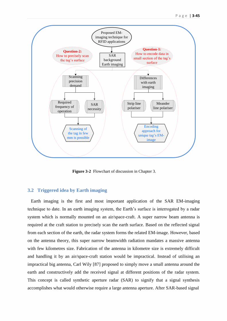
P a g e | 3-45
Figure 3-2 Flowchart of discussion in Chapter 3.
3.2 Triggered idea by Earth imaging
Earth imaging is the first and most important application of the SAR EM-imaging
technique to date. In an earth imaging system, the Earth’s surface is interrogated by a radar
system which is normally mounted on an air/space-craft. A super narrow beam antenna is
required at the craft station to precisely scan the earth surface. Based on the reflected signal
from each section of the earth, the radar system forms the related EM-image. However, based
on the antenna theory, this super narrow beamwidth radiation mandates a massive antenna
with few kilometres size. Fabrication of the antenna in kilometre size is extremely difficult
and handling it by an air/space-craft station would be impractical. Instead of utilising an
impractical big antenna, Carl Wily [87] proposed to simply move a small antenna around the
earth and constructively add the received signal at different positions of the radar system.
This concept is called synthetic aperture radar (SAR) to signify that a signal synthesis
accomplishes what would otherwise require a large antenna aperture. After SAR-based signal
Question-2:
How to precisely scan
the tag’s surface
Question-1:
How to encode data in
small section of the tag’s
surface
Scanning
precision
demand
Required
frequency of
operation
SAR
necessity
Scanning of
the tag in few
mm is possible
Differences
with earth
imaging
Strip line
polariser
Meander
line polariser
Encoding
approach for
unique tag’s EM-
image
Proposed EM-
imaging technique for
RFID applications
SAR
background
Earth imaging

P a g e | 3-46
Figure 3-3 Reflection strength based on terrain roughness in earth imaging system [88].
processing, the strength of the reflected signal from each section of the Earth’s surface is
linked to its EM-image and shows the terrain of the Earth’s surface. Rough surfaces result in
higher reflection and therefore a brighter part in the EM-image; a building or mountain for
example. An impinged signal on a flat surface is reflected in the opposite direction, by Snell’s
law, hence radar receives no energy and a black image is formed. Figure 3-3 shows the
principle of image brightness in an earth imaging system. This working basis may initiate the
idea of shaping the RFID tag surface in such a way to create a unique image when
illuminated by a proper EM signal. This is discussed in more detail in the following sections.
3.3 Precise scanning of the tag surface
The accuracy of scanning in the proposed image-based system directly relates to the
associated data encoding capacity. Therefore, to find out what is the minimum required
scanning precession, one should know about the expected content capacity of the chipless
RFID system. On the other hand, the size of the tag shall also be limited to certain values. For
many RFID applications, the size of a credit card (85 × 55 mm2) appears to be the maximum
allowable size of the RFID tag [11, 47].
The expected content capacity of the chipless RFID systems is more difficult to standardise
as every industry has its own requirements and expectations. However, many research entities
Flat surface Forest Different
plantsMountain
Earth imaging system
Earth surface :
RADAR image :
Radar signal
Reflected signal
toward radar

P a g e | 3-47
assume 50 bits data encoding capacity for a chipless tag structure as the ultimate capacity of
these systems [16, 17, 89]. This may suggest one bit/cm 2 as the very satisfying data encoding
capacity of a chipless RFID system.
250
1 /8.5 5.4
Encoding capacity bit cm
(3.1)
Therefore, the targeted scanning precession in the proposed image-based system should be
around 10 mm. This means that the reflected signal from each one cm2 of the tag surface shall
be processed separately by the reader. The straight forward approach for analysing the effect
of each small section of the tag is to utilise a reader antenna in which its radiation pattern
illuminates every 10 mm of the tag surface separately. This illumination area is known as the
footprint of the reader on the tag surface as shown in Figure 3-1. To interpret this footprint
size with the 3-dB beamwidth of the reader antenna, the reading distance is required. The
normal reading distance of the chipless RFID system is currently limited to 50 cm as the tag
has no internal power source and the reader relies only on the backscattered power [90].
Figure 3-4 shows the reader footprint on the tag surface with two image resolutions. The
range and cross-range resolutions are defined by ρr and ρσ respectively. These two resolutions
with the reading distance (d) and 3-dB beamwidth of the antenna are also shown in
Figure 3-4.
3.3.1 Frequency band selection
As discussed earlier, a rough estimate of 10 mm scan resolution requirement has already
been gained through the maximum expected data encoding capacity of the chipless RFID
system. To find the best suitable frequency range(s) for the proposed image-based system, it
is necessary to relate the parameters of Figure 3-4 to each other. The image resolution,
whether in range or cross-range, simply corresponds to d and 3-dB beamwidth (θ3-dB) of the
antenna through:
3.tan( ) ; ,i dBd where i r cr (3.2)

P a g e | 3-48
Figure 3-4 Reader footprint on tag structure.
This formula is figuratively shown in Figure 3-5. The expected beamwidth of the reader
antenna is very narrow and normally varies between 1-6° as stated above. Creation of such a
narrow beamwidth requires a very large antenna size as the antenna beamwidth inversely
relates to the antenna physical size. The exact relation between the antenna’s beamwidth and
its physical size depends on the aperture illumination function, which controls the main beam
and side lobes of the radiation pattern of the antenna. However, a practical rule-of-thumb for
typical illumination functions expresses the beamwidth in terms of aperture size and the
wavelength as follows:
3dBD
(3.3)
where θ is the 3-dB beamwidth of the antenna in radians, λ is the wavelength, D is the
antenna physical size and α is a constant reflecting the main lob widening due to the
weighting aperture. For a uniform aperture weighting, α ≈ 0.89 and hence (3.2) is changed to
3 50dBD
when θ is measured in degrees. By assuming 1° beamwidth demand, the
required aperture size is depicted in Figure 3-6 based on various frequency ranges. The actual
required antenna size is also shown for three common ISM bands of 2.4, 24 and 60 GHz.
Tag
ρcr
ρr
3-dB
beamwidth
d
Reader antenna
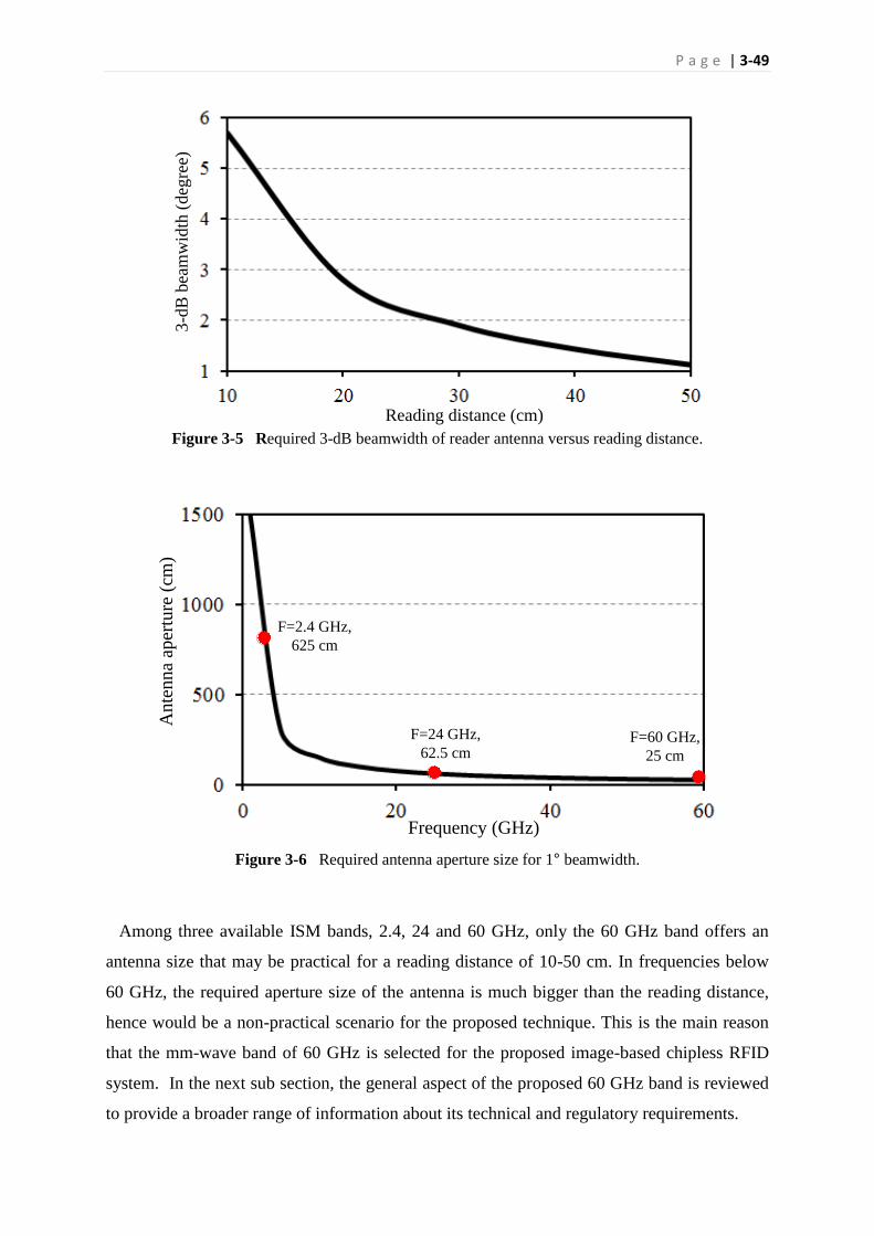
P a g e | 3-49
Figure 3-5 Required 3-dB beamwidth of reader antenna versus reading distance.
Figure 3-6 Required antenna aperture size for 1° beamwidth.
Among three available ISM bands, 2.4, 24 and 60 GHz, only the 60 GHz band offers an
antenna size that may be practical for a reading distance of 10-50 cm. In frequencies below
60 GHz, the required aperture size of the antenna is much bigger than the reading distance,
hence would be a non-practical scenario for the proposed technique. This is the main reason
that the mm-wave band of 60 GHz is selected for the proposed image-based chipless RFID
system. In the next sub section, the general aspect of the proposed 60 GHz band is reviewed
to provide a broader range of information about its technical and regulatory requirements.
Reading distance (cm)
3-d
B b
eam
wid
th (
deg
ree)
Frequency (GHz)
Ante
nna
aper
ture
(cm
)
F=2.4 GHz,
625 cm
F=24 GHz,
62.5 cmF=60 GHz,
25 cm
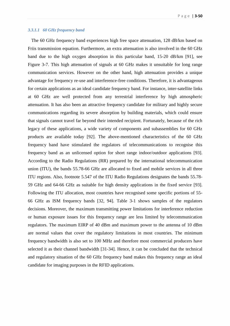
P a g e | 3-50
3.3.1.1 60 GHz frequency band
The 60 GHz frequency band experiences high free space attenuation, 128 dB/km based on
Friis transmission equation. Furthermore, an extra attenuation is also involved in the 60 GHz
band due to the high oxygen absorption in this particular band, 15-20 dB/km [91], see
Figure 3-7. This high attenuation of signals at 60 GHz makes it unsuitable for long range
communication services. However on the other hand, high attenuation provides a unique
advantage for frequency re-use and interference-free conditions. Therefore, it is advantageous
for certain applications as an ideal candidate frequency band. For instance, inter-satellite links
at 60 GHz are well protected from any terrestrial interference by high atmospheric
attenuation. It has also been an attractive frequency candidate for military and highly secure
communications regarding its severe absorption by building materials, which could ensure
that signals cannot travel far beyond their intended recipient. Fortunately, because of the rich
legacy of these applications, a wide variety of components and subassemblies for 60 GHz
products are available today [92]. The above-mentioned characteristics of the 60 GHz
frequency band have stimulated the regulators of telecommunications to recognise this
frequency band as an unlicensed option for short range indoor/outdoor applications [93].
According to the Radio Regulations (RR) prepared by the international telecommunication
union (ITU), the bands 55.78-66 GHz are allocated to fixed and mobile services in all three
ITU regions. Also, footnote 5.547 of the ITU Radio Regulations designates the bands 55.78-
59 GHz and 64-66 GHz as suitable for high density applications in the fixed service [93].
Following the ITU allocation, most countries have recognised some specific portions of 55-
66 GHz as ISM frequency bands [32, 94]. Table 3-1 shows samples of the regulators
decisions. Moreover, the maximum transmitting power limitations for interference reduction
or human exposure issues for this frequency range are less limited by telecommunication
regulators. The maximum EIRP of 40 dBm and maximum power to the antenna of 10 dBm
are normal values that cover the regulatory limitations in most countries. The minimum
frequency bandwidth is also set to 100 MHz and therefore most commercial producers have
selected it as their channel bandwidth [31-34]. Hence, it can be concluded that the technical
and regulatory situation of the 60 GHz frequency band makes this frequency range an ideal
candidate for imaging purposes in the RFID applications.

P a g e | 3-51
Table 3-1 Available spectrum on 60 GHz band
Country/Region Frequency (GHz)
Australia 59.4-62.9
USA & Canada & Korea 57-64
Japan 59-66
Europe 57-66
China 59-64
EIRPmax 40dBm
Ptrans 10dBm
bandwidthmin 100 MHz
Figure 3-7 Specific attenuation due to atmospheric gases [91].
3.3.2 Lower printed tag cost at mm-wave
It is well known that optimal tag reflection corresponds to metallic tags that are at least as
thick as the skin depth, or the electrical current depth necessary to completely reflect the EM
wave due to the surface AC currents. The skin depth as a function of radio frequency and
material conductivity is shown in Figure 3-8.
Frequency (GHz)
2 10 100
0.01
0.001
0.1
1
10
100
Spec
ific
att
enuat
ion
(dB
/km
)
Dry air
Total
Water vapour
Total
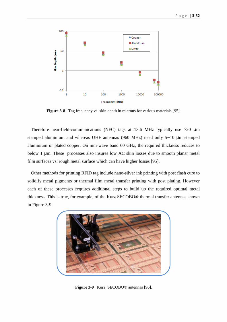
P a g e | 3-52
Figure 3-8 Tag frequency vs. skin depth in microns for various materials [95].
Therefore near-field-communications (NFC) tags at 13.6 MHz typically use >20 μm
stamped aluminium and whereas UHF antennas (960 MHz) need only 5~10 μm stamped
aluminium or plated copper. On mm-wave band 60 GHz, the required thickness reduces to
below 1 μm. These processes also insures low AC skin losses due to smooth planar metal
film surfaces vs. rough metal surface which can have higher losses [95].
Other methods for printing RFID tag include nano-silver ink printing with post flash cure to
solidify metal pigments or thermal film metal transfer printing with post plating. However
each of these processes requires additional steps to build up the required optimal metal
thickness. This is true, for example, of the Kurz SECOBO® thermal transfer antennas shown
in Figure 3-9.
Figure 3-9 Kurz SECOBO® antennas [96].

P a g e | 3-53
However as the RFID frequency of operation continues to increase, the required skin depth
thickness decreases. Thus from the perspective of the metal film thicknesses necessary for
efficient interrogation signal reflection, there are tremendous advantages to utilizing a higher
frequencies for chipless RFID operation. Thinner metal RFID antennas mean more viable
lower cost tag fabrication techniques such as inkjet and metal foil transfer can be used with
greater throughput and yield, though surface roughness also becomes more important at
higher frequency owing to high current densities near the surface of the metal tags.
3.3.3 Synthetic aperture radar necessity
Recalling from Section 3.2, the SAR technique proposed for earth imaging applications, as
carrying a kilometre sized antenna by an air/space-craft station is impractical. Although in the
RFID application, the required antenna size for 1° beamwidth requirement is only 25 cm,
Figure 3-6. Therefore, it appears that a single antenna would be sufficient for the required
precision scanning of the tag. However, one should note that the calculated beamwidth by
(3.3) is only valid for the far field region of the antenna. If the measurement point locates
inside the near field, then it is unlikely to expect 1° beamwidth. The far field distance of the
antenna with 25 cm aperture size at 60 GHz is 25 m that is far beyond the reading zone of the
chipless RFID systems:
2 2
3
2 2 (0.25)25
5 10far field
DR m
(3.4)
SAR would provide a solution for this scenario. A small antenna at 60 GHz with short
farfield distance is utilised at the reader side. This antenna generates a large beamwidth due
to its small physical size and hence is not capable of providing the required scanning
precision. However, if the antenna moves around the tag to create a synthetic aperture then
the post signal processing results in a narrow beamwidth of 1~5° order depending on the
synthetic aperture length.
Therefore it can be concluded that the practical limitation of carrying a kilometre sized
antenna necessitates the SAR technique for earth imaging purpose, while the technical
limitation of farfield distance mandates the SAR approach for RFID application. This would
be similar to a body EM-imaging application. In human body imaging, the usage of a single
large antenna with narrow beamwidth is feasible. However, maximum transmission power on

P a g e | 3-54
human body is limited due to the regulations. Therefore, a small antenna(s) with low
transmission power on the SAR working basis is utilised to meet the regulation requirements
and simultaneously provide the required high image resolution.
Finally as the conclusion to Section 3.3, it appears that the scanning of the tag surface in
millimetre order at the reading distance of 10-50 cm is technically and practically feasible
only at the ISM band 60 GHz and above; 95 GHz for example. However, due to the far field
limitation, the synthetic aperture radar technique shall be utilised at the reader side. This
means that the relative movement of the reader and tag is an integral part of the proposed
theory. However as will be introduced in Chapter 8 of this dissertation, it is possible to
combine the multiple input multiple output (MIMO)-based technique with the current
proposal to eliminate the physical movement necessity and significantly improve the reading
time of the proposed theory [82].
3.4 Tag shaping for unique EM-image purposes
It was discussed that the scanning of the tag surface is technically feasible at mm-wave
bands. The next step of maturing the idea of imaging for the RFID application is to design a
chipless tag in such a way that the tag obtains a unique EM-image. To shape the tag’s surface
for creation of a unique EM-image, no component other than paper and conductive ink shall
be considered otherwise the tag cost would exceed industry expectations. The unique EM-
image of the tag therefore shall be constructed by combining conductive and non-conductive
sections on the tag’s surface. As the dielectric part has a rougher surface, then the expectation
is to have a brighter image than that of the conductive part, based on previous knowledge
from the earth imaging application, Figure 3-3. Based on this information, one may suggest a
structure similar to a barcode as shown in Figure 3-10. Conductive and non-conductive strips
create different levels of reflection on the reader side, hence a unique EM-image would be
created with different arrangement of the strips on the tag surface. To examine this idea, two
separate conductive and dielectric strips are simulated through 3-D full wave CST software
on the 57-64 GHz band as the frequency band of operation. The strips are illuminated by a
linearly polarised plane wave and their levels of backscattered signals on the reader side are
measured. The results are shown in Figure 3-11 in which the reading distance is 30 cm, the
incident electric field is one V/m, and it is parallel to the main axis of the strip. The first
interesting aspect of the result is that the reflection from the conductive strip is higher than
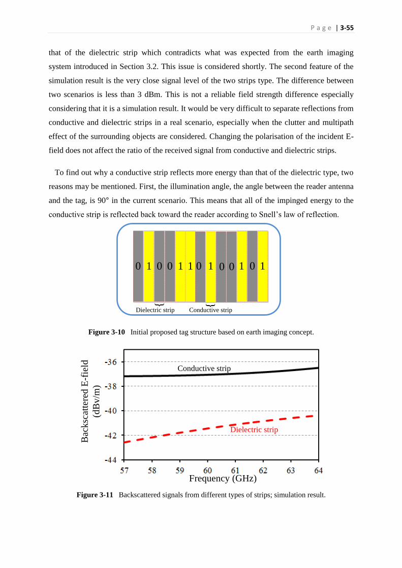
P a g e | 3-55
that of the dielectric strip which contradicts what was expected from the earth imaging
system introduced in Section 3.2. This issue is considered shortly. The second feature of the
simulation result is the very close signal level of the two strips type. The difference between
two scenarios is less than 3 dBm. This is not a reliable field strength difference especially
considering that it is a simulation result. It would be very difficult to separate reflections from
conductive and dielectric strips in a real scenario, especially when the clutter and multipath
effect of the surrounding objects are considered. Changing the polarisation of the incident E-
field does not affect the ratio of the received signal from conductive and dielectric strips.
To find out why a conductive strip reflects more energy than that of the dielectric type, two
reasons may be mentioned. First, the illumination angle, the angle between the reader antenna
and the tag, is 90° in the current scenario. This means that all of the impinged energy to the
conductive strip is reflected back toward the reader according to Snell’s law of reflection.
Figure 3-10 Initial proposed tag structure based on earth imaging concept.
Figure 3-11 Backscattered signals from different types of strips; simulation result.
Dielectric strip
{ {
Conductive strip
0 1 00 0 01 1 1 110 0
Frequency (GHz)
Bac
ksc
atte
red E
-fie
ld
(dB
v/m
)
Conductive strip
Dielectric strip
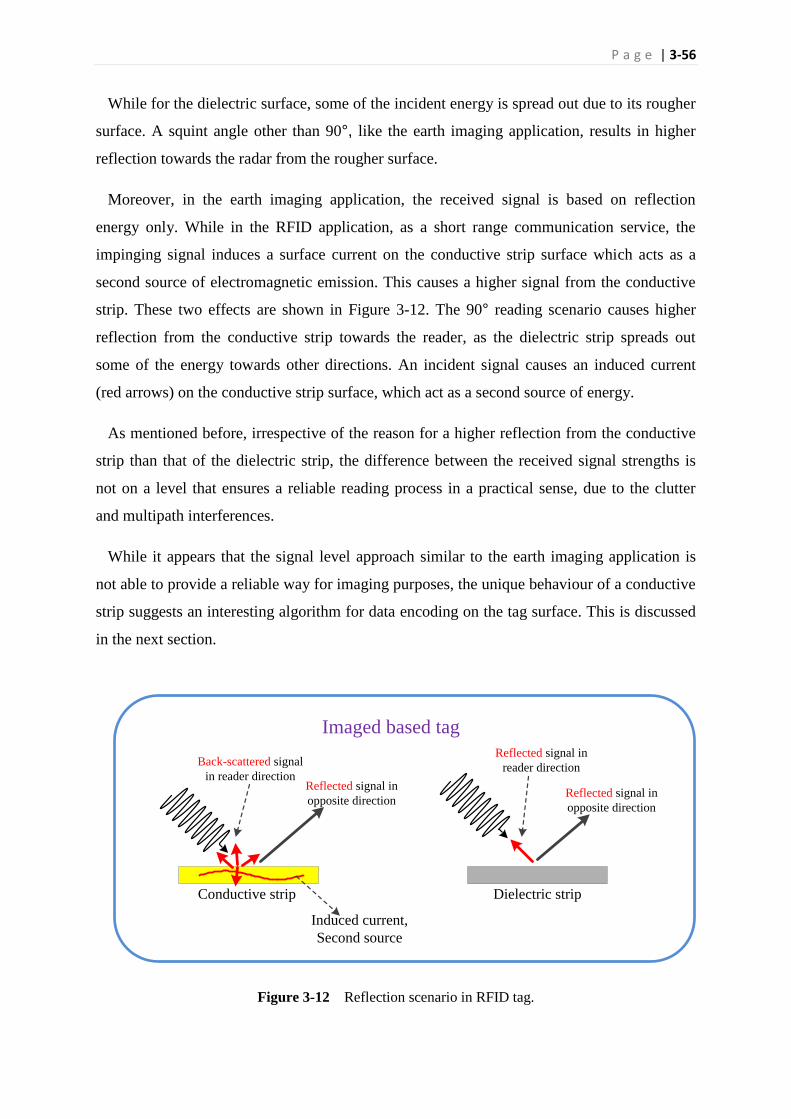
P a g e | 3-56
While for the dielectric surface, some of the incident energy is spread out due to its rougher
surface. A squint angle other than 90°, like the earth imaging application, results in higher
reflection towards the radar from the rougher surface.
Moreover, in the earth imaging application, the received signal is based on reflection
energy only. While in the RFID application, as a short range communication service, the
impinging signal induces a surface current on the conductive strip surface which acts as a
second source of electromagnetic emission. This causes a higher signal from the conductive
strip. These two effects are shown in Figure 3-12. The 90° reading scenario causes higher
reflection from the conductive strip towards the reader, as the dielectric strip spreads out
some of the energy towards other directions. An incident signal causes an induced current
(red arrows) on the conductive strip surface, which act as a second source of energy.
As mentioned before, irrespective of the reason for a higher reflection from the conductive
strip than that of the dielectric strip, the difference between the received signal strengths is
not on a level that ensures a reliable reading process in a practical sense, due to the clutter
and multipath interferences.
While it appears that the signal level approach similar to the earth imaging application is
not able to provide a reliable way for imaging purposes, the unique behaviour of a conductive
strip suggests an interesting algorithm for data encoding on the tag surface. This is discussed
in the next section.
Figure 3-12 Reflection scenario in RFID tag.
Conductive strip Dielectric strip
Imaged based tag
Induced current,
Second source
Reflected signal in
opposite direction
Reflected signal in
reader direction
Reflected signal in
opposite direction
Back-scattered signal
in reader direction

P a g e | 3-57
3.4.1 Strip line as an EM-polariser
In the previous work described in Section 3.2, the main goal was to measure the received
signal level based on various illumination angles and polarisation schemes from different
strip types. Although working on the basis of a different received signal level did not provide
a reliable approach for the data encoding algorithm on a chipless tag structure, a very
interesting phenomenon was observed during the simulation. It was noticed that the
backscattered signal from a narrow conductive strip shows elliptical polarisation behaviour
while the strip is illuminated by a linearly polarised signal. This means that the conductive
strip is capable of changing the polarisation of the incident signal. This issue has been
considered more seriously aiming for possible application in the chipless RFID system. It was
found that for a narrow conductive strip, the backscattered signal may include a polarisation
component that is orthogonal to the polarisation of the incident signal, hence the conductive
strip acts as an EM-polariser. The de-polarisation aspect of the conductive strip suggests
working on a cross-polar basis instead of a co-polar basis, which most conventional
techniques are. This provides significant superiority as a cross-polar working basis may
eliminate or severely reduce noise, clutter and multipath effects on the system performance.
Those factors are normally a significant concern in RFID systems and are considered the
main limiting features. The theory behind this unusual behaviour of the conductive strip as an
EM-polariser, is discussed here and the potential advantages and applications are considered
in more detail in the next chapters.
3.4.1.1 Diffraction, Kobayashi potentials
Different phenomena are involved when a conductive strip is illuminated by an EM-signal,
for instance, reflection, refraction and diffraction. As a strip has a finite surface with straight
edges, it can behave differently based on the polarisation and frequency of the incident wave
as well as strip size and its orientation. Reflection based on Snell’s law is the normal
behaviour that is expected for a wide strip, compared to the wavelength. However, when the
strip is narrow enough, diffraction would be of more concern and act as the dominant
phenomenon. In prior decades, many studies investigated diffraction from a metallic strip or a
slot in a metal plane using various numerical and analytical techniques [97-104]. All research
and studies on diffraction can be summarised as follows [105]:

P a g e | 3-58
Geometric Optics (GO) [98]
Physical Optic (PO) [99]
Geometrical Theory of Diffraction (GTD) [100]
Uniform Asymptotic Theory of Diffraction (UAD) [101]
Uniform Theory of Diffraction (UTD) [100]
Physical Theory of Diffraction (PTD) [102]
Spectral Theory of Diffraction (STD) [103]
Method of Equivalent Current (MEC) [104]
Hybrid methods
Each method has its own advantages and limitations. Among them, geometrical optics
(GO), physical optics (PO), and uniform theory of diffraction (UTD) are the most common
approaches. The Kobayashi potential (KP) method is an analytico-numerical technique used
as an alternative to previously mentioned techniques with more accurate results and less
procedure complexity [106]. Diffraction by a conductive strip on a dielectric slab has been
thoroughly studied as a title of PhD thesis by Imran [107]. He formulated the far field pattern
and induced surface current on an infinite strip etched to a dielectric slab based on the
polarisation of the incident plane wave. This sub-section is a snap shot of his work related to
the current research.
Figure 3-13 shows the geometry of the diffraction phenomenon where a conductive strip
with negligible thickness etched on a dielectric slab is illuminated with a plane wave. The
plane wave incident angle is Φ0. The strip width is 2a and it is infinite in z direction. The
diffracted wave depends on the polarisation of the plane wave. Two separate polarisations are
considered: (i) Parallel-polarisation, 0 zE E a , and (ii) Orthogonal-polarisation, 0 xE E a .
In the parallel polarisation, the incident E-field is parallel to the main axis of the strip, the
backscattered signal may have components in x or z direction. The co-polar and cross-polar
components are defined by (3.5) and (3.6) respectively [107]:
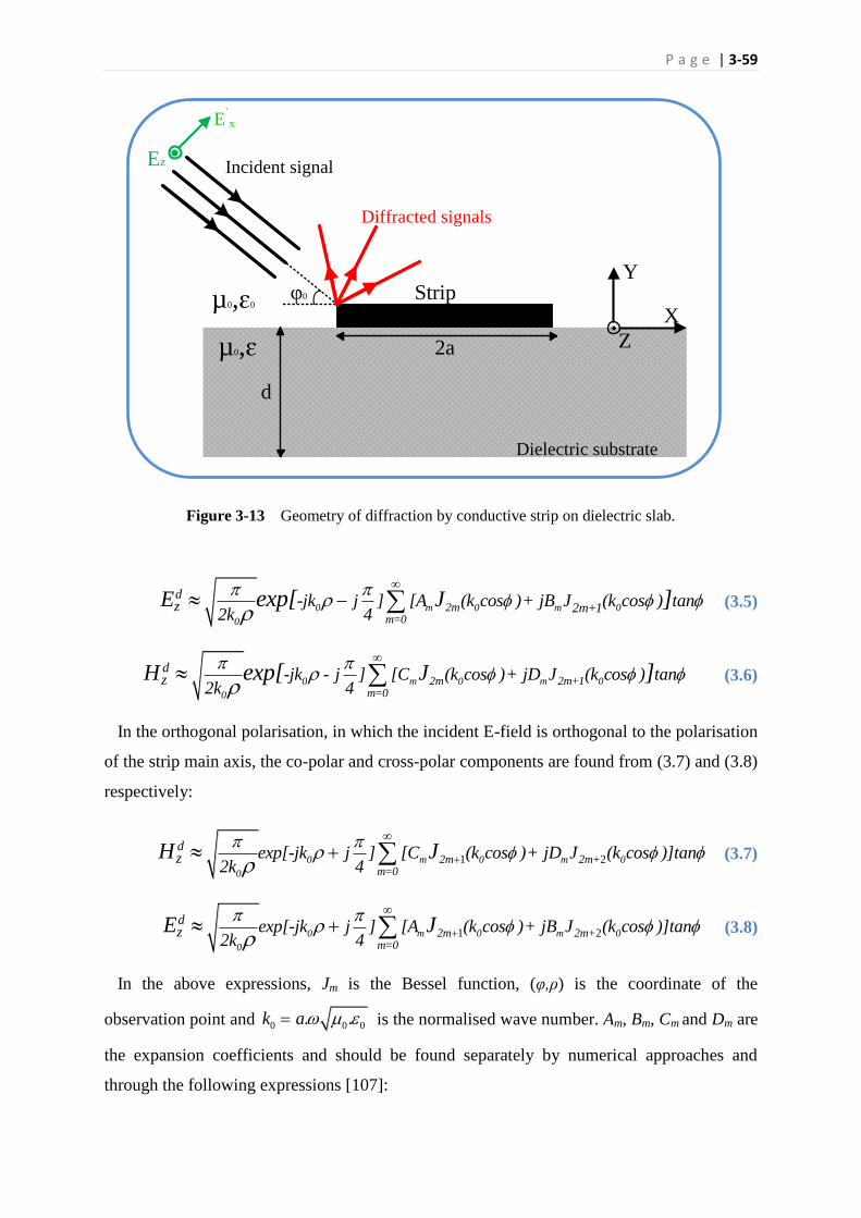
P a g e | 3-59
Figure 3-13 Geometry of diffraction by conductive strip on dielectric slab.
0 m 0 m 0
0
2mm=0
d2m+1z -jk j ] [A (k cos )+ jB J (k cos ) tan
2k 4E Jexp[ ]
(3.5)
0 m 0 m 0
0
2m 2m+1m=0
dz -jk - j ] [C (k cos )+ jD J (k cos ) tan
2k 4H Jexp[ ]
(3.6)
In the orthogonal polarisation, in which the incident E-field is orthogonal to the polarisation
of the strip main axis, the co-polar and cross-polar components are found from (3.7) and (3.8)
respectively:
1 20 m 0 m 0
0
2m 2m+m=0
dz exp[-jk j ] [C (k cos )+ jD J (k cos )]tan
2k 4H J
(3.7)
1 20 m 0 m 0
0
2m 2m+m=0
dz exp[-jk j ] [A (k cos )+ jB J (k cos )]tan
2k 4E J
(3.8)
In the above expressions, Jm is the Bessel function, (φ,ρ) is the coordinate of the
observation point and 0 0 0. .k a is the normalised wave number. Am, Bm, Cm and Dm are
the expansion coefficients and should be found separately by numerical approaches and
through the following expressions [107]:
µ0,ɛ
µ0,ɛ0 φ0
d
2a
X
Y
Z
Dielectric substrate
Strip
Ez Incident signal
Diffracted signals
E`x

P a g e | 3-60
0 2 0 0
0
[ (2 ,2 ; )][ ] [ ( cos )]m m n
m
G m n k C MA M J k
(3.9)
0 2 1 0 0
0
[ (2 1,2 1; )][ ] [ ( cos )]m m n
m
G m n k D MB Mj J k
(3.10)
2
0 0 0 2 1 0 0
0
[ (2 ,2 1; )][ ] tan( )[ ( cos )]m m n
m
H m n k A MC Z j J k
(3.11)
2
0 0 0 2 2 0 0
0
[ (2 1,2 2; )][ ] tan( )[ ( cos )]m m n
m
H m n k B MD Z J k
(3.12)
where n = 0, 1, 2,…, M is the admittance parameter and
02 20
0
00
( ). ( )( , ; )
( ). ( )( , ; )
J JG k d
k
J JH k d
(3.13)
A comprehensive derivations of the above expressions based on the different values of the
parameters has been provided in [107]. Among these results, the relation between the strip
width and the cross-polar component is the concern of the current application. It is shown in
[107] that the normalised wave number affects the strength of the cross-polar components of
the diffracted signal. Moreover, the cross-polar component is also dependent on the angle of
observation. For a certain value of the normalised wave number, that is relevant to the strip
width, the maximum cross-polar component is achievable over a wide range of observation
angles. The co-polar and cross-polar components of the diffracted signal are figuratively
shown in Figure 3-14 that proves that a well-designed strip is capable of creating a cross-
polar component while illuminated by a linear polarised incident signal.
This is a significant result of the diffraction effect. It simply means that for a certain strip
with adequate dimensions, it is possible to expect cross-polar components in the
backscattered signal with respect to the incident wave. Hence, the simple structure of a strip
line acts as an effective EM-polariser. This interesting aspect of the diffraction is used on the
current research for providing an effective data encoding algorithm in a chipless tag.
Therefore, one may recall that diffraction was the main issue in the barcode system as it
limits the barcodes data encoding capacity and its reading range. In contrary, the proposed
approach of EM-imaging in chipless RFID system is fully based on the diffraction effect.

P a g e | 3-61
Figure 3-14 Co- and cross-polar components of diffracted signals, linear scale.
3.4.1.2 Cross-polarised resonance
In the previous section, the cross-component of the backscattered signal from a narrow strip
with infinite length due to the diffraction effect has been discussed. This simply means that
diffracted signal by the strip edge creates a cross-polar component. Moreover, due to the
diffraction effect, it is also possible to maximise the backscattered cross-polar component by
utilising the resonance behaviour of the strip structure. In a real scenario, the strip has a finite
length, hence it is possible to design the length of the strip to resonate at a particular
frequency. Maximising the backscattered cross-component, one may suggest orienting the
strip at 45˚ angle with respect to the incident plane wave. This causes the induced current on
the strip surface, as a secondary source of EM-wave, to emit signals in both co- and cross-
polar directions as shown in Figure 3-15. It is important to note that in this scenario, the
length of the strip plays the major role while in diffraction phenomenon, the strip width was
the main concern.
The strip line shown in Figure 3-15 is simulated as an E-polariser through full wave EM
solver CST microwave studio. The strip is illuminated with a linearly polarised plane wave
while the incident E-field maintains a 45˚ angle with the strip axis. Two E-field probes are
oriented at a certain distance, 30 cm for example, to measure the backscattered signal
Observation angles (degree)
Dif
frac
ted
fie
ld,
no
rmal
ised
E-pol./
Cross-component
H-pol./
Cross-component
E-pol/Co-component
H-pol./Co-component
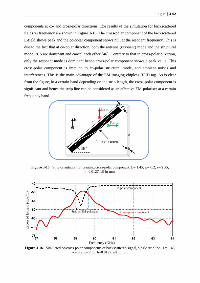
P a g e | 3-62
components at co- and cross-polar directions. The results of the simulation for backscattered
fields vs frequency are shown in Figure 3-16. The cross-polar component of the backscattered
E-field shows peak and the co-polar component shows null at the resonant frequency. This is
due to the fact that at co-polar direction, both the antenna (resonant) mode and the structural
mode RCS are dominant and cancel each other [46]. Contrary to that in cross-polar direction,
only the resonant mode is dominant hence cross-polar component shows a peak value. This
cross-polar component is immune to co-polar structural mode, and ambient noises and
interferences. This is the main advantage of the EM-imaging chipless RFID tag. As is clear
from the figure, in a certain band depending on the strip length, the cross-polar component is
significant and hence the strip line can be considered as an effective EM-polariser at a certain
frequency band.
Figure 3-15 Strip orientation for creating cross-polar component, L= 1.45, w= 0.2, ε= 2.55,
h=0.0127, all in mm.
Figure 3-16 Simulated co/cross-polar components of backscattered signal, single stripline , L= 1.45,
w= 0.2, ε= 2.55, h=0.0127, all in mm.
45°
Induced current
LEi
Ed-cross
Ed-coW
h
ε
Rec
eiv
ed E
-fie
ld (
dB
v/m
)
Frequency (GHz)
Cross-polar component
Co-polar component
Strip as EM-polarizer

P a g e | 3-63
3.4.1.3 Multiple strips effect
It will be shown soon that to accommodate the required RCS power level at the receiver
side, it is required to utilise more than one strip line or any other polariser on the tag surface.
This is almost mandatory for satisfying the signal to noise ratio (SNR). Therefore, it is
important to explore the effect of multiple strip lines on the backscattered signal.
A. Multiple strips with the same dimension
If an accurate and precise fabrication process is utilised for tag manufacturing, then it is
reasonable to expect that all the strip lines have exactly the same dimensions. Obviously, if
the strip lines are the same length and width, then a similar response to what is shown in
Figure 3-16, with a higher received E-field level, is expected. To validate this expectation,
five strip lines with the same dimension are placed near to each other (one mm distance). The
simulated co- and cross-polar backscattered E-fields are shown in Figure 3-17. Comparing
Figure 3-16 and Figure 3-17, one notices the followings phenomena:
i) Resonance frequency shifts from 59.5 GHz to 58.2 GHz, about 1.3 GHz.
ii) Resonance bandwidth spread from 0.7 to one GHz.
iii) Amplitude of the backscattered signal increases by approximately 6.5 dB from -49 dB/m
to -42.5 dB/m. This is approximately five times (10 × log5 = 7 dB) amplification as expected.
Both i) and ii) can be related to the coupling among strips as they were placed very close to
each other (one mm). This means that Figure 3-17 is not simply a multiplication of
Figure 3-16. However, the initial expectation on the received power level has been almost
confirmed.
B. Multiple strips with slightly different lengths
In the previous section, the effect of multiple strips with the same dimension has been
considered. It is very important to explore the behaviour of the received signal on co- and
cross-polar directions if strips have slightly different dimensions; lengths for example.
Shortly, the importance of this case is realised when the tag is printed by an ink-jet printer.
The printed strip lines do not have exactly the same length because of printing inaccuracy.

P a g e | 3-64
Figure 3-17 a) Five strip lines with same length, b) Simulated co/cross-polar backscattered signals.
To simulate this case, multiple strips with slightly different lengths are considered while
they are again placed close (one mm) to each other. Five strip lines, whose lengths vary from
1.6 to 1.7 mm, are considered. Figure 3-18 shows the simulation results of the backscattered
fields and for ease of comparison, the result of a single strip is also reproduced in this figure.
It is clear from Figure 3-18 that the RCS response from multiple strips with different lengths
does not show any resonance behaviour. There are some fluctuations on the received signal
level, but detection of the resonances is very difficult if not impossible. The co-polar
component of the E-field is 5-10 dB higher than that of the cross-polar component.
Irrespective of higher co-polar level, the proposed system is a cross-polar system. The
advantages of the cross-polar based technique are revealed during the measurement process.
a)
hε 1 mm
L=1.5 m
m
Ed-cross
Ed-coEi
Strips as EM-polariser
Rec
eiv
ed E
-fie
ld (
dB
v/m
)
Cross-polar component
Co-polar componentb)
Frequency (GHz)
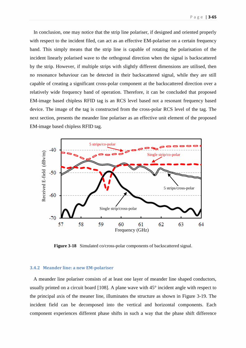
P a g e | 3-65
In conclusion, one may notice that the strip line polariser, if designed and oriented properly
with respect to the incident filed, can act as an effective EM-polariser on a certain frequency
band. This simply means that the strip line is capable of rotating the polarisation of the
incident linearly polarised wave to the orthogonal direction when the signal is backscattered
by the strip. However, if multiple strips with slightly different dimensions are utilised, then
no resonance behaviour can be detected in their backscattered signal, while they are still
capable of creating a significant cross-polar component at the backscattered direction over a
relatively wide frequency band of operation. Therefore, it can be concluded that proposed
EM-image based chipless RFID tag is an RCS level based not a resonant frequency based
device. The image of the tag is constructed from the cross-polar RCS level of the tag. The
next section, presents the meander line polariser as an effective unit element of the proposed
EM-image based chipless RFID tag.
Figure 3-18 Simulated co/cross-polar components of backscattered signal.
3.4.2 Meander line: a new EM-polariser
A meander line polariser consists of at least one layer of meander line shaped conductors,
usually printed on a circuit board [108]. A plane wave with 45° incident angle with respect to
the principal axis of the meaner line, illuminates the structure as shown in Figure 3-19. The
incident field can be decomposed into the vertical and horizontal components. Each
component experiences different phase shifts in such a way that the phase shift difference
Frequency (GHz)
Rec
eiv
ed E
-fie
ld (d
Bv/m
)
Single strip/cross-polar
5 strips/cross-polar
5 strips/co-polar
Single strip/co-polar
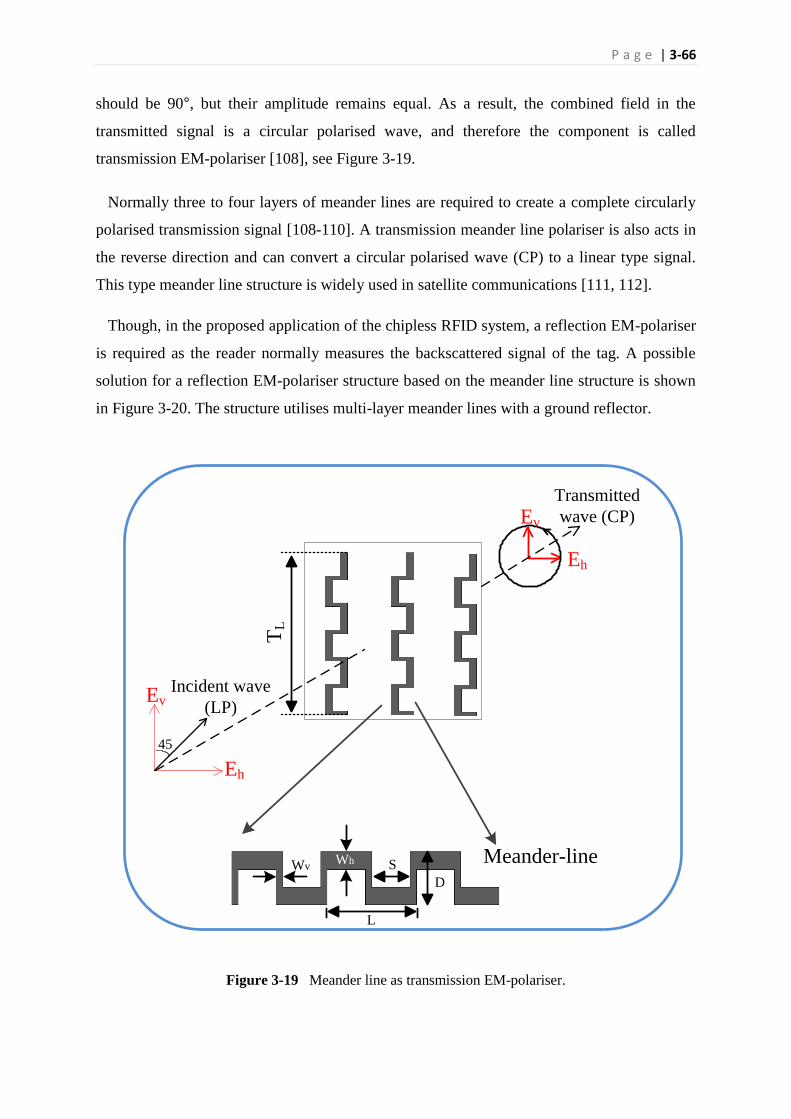
P a g e | 3-66
should be 90°, but their amplitude remains equal. As a result, the combined field in the
transmitted signal is a circular polarised wave, and therefore the component is called
transmission EM-polariser [108], see Figure 3-19.
Normally three to four layers of meander lines are required to create a complete circularly
polarised transmission signal [108-110]. A transmission meander line polariser is also acts in
the reverse direction and can convert a circular polarised wave (CP) to a linear type signal.
This type meander line structure is widely used in satellite communications [111, 112].
Though, in the proposed application of the chipless RFID system, a reflection EM-polariser
is required as the reader normally measures the backscattered signal of the tag. A possible
solution for a reflection EM-polariser structure based on the meander line structure is shown
in Figure 3-20. The structure utilises multi-layer meander lines with a ground reflector.
Figure 3-19 Meander line as transmission EM-polariser.
45
Incident wave
(LP)
Transmitted
wave (CP)
D
L
WhWv S Meander-line
Eh
Ev
Ev
Eh
TL
P a g e | 3-67
The linearly polarised incident wave (Ei) is converted to a circular polarisation wave while
passing the multi-layer meander line structure. For the x-polarised incident signal shown in
Figure 3-20, the passed signal from the meander line structure is a left hand circular polarised
(LHCP) wave, for example. This wave is completely reflected back by the ground plane
while its rotation direction will be reversed. Hence the new wave with right hand circular
polarisation (RHCP) is inserted in the multi-layer meander line structure. This signal is
converted to a linear polarised wave as the meander line changes the input circular polarised
(CP) signal to a linearly polarised (LP) wave. However, the E-field of the final reflected wave
(Er) is orthogonal to the direction of the E-field of the original incident wave (Ei). Hence the
goal of the meander line as a reflection EM-polariser is achieved.
While the proposed approach of the multi-layer meander line with a ground plane reflector
is technically appropriate for the proposed application of the chipless RFID system, it would
not be a suitable solution for RFID tag structure. The multi-layer structure of the tag
contradicts the expected sub cent tag cost that is only addressed through a single layer
printable tag structure. Therefore, to propose a single layer structure, the meander line
dimensions have been re-designed based on a diffraction and resonance principles similar to
those for strip line polariser as introduced in Section 3.4.1. Hence, only one layer meander
line is utilised with no ground plane. This means that the parameters of the meander line
structure as shown in Figure 3-19 are designed to maximize the cross-polar component of the
backscattered signal. Similar to the case of the strip line, again both diffraction and resonance
behavior of the meander line are utilised simultaneously for the maximum cross-polar
component. The expectation is to achieve better performance from the meander line due to
the increased design freedom. While the strip line has mainly two design parameters: strip
width and length, in the meander line polariser there are more design parameters: Wh, Wv, D,
S and L that provides more design flexibility, see Figure 3-19.
A single layer meander line is designed through parameter optimisation in CST aiming to
provide the highest cross-polar component backscattered RCS. The structure is assumed to
have the same length that for the strip line for comparison purposes. The simulation result is
shown in Figure 3-21 while the parameter of the design for the strip line and meander line are
as follows:
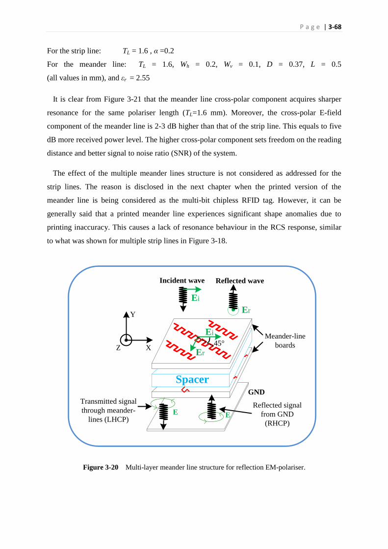
P a g e | 3-68
For the strip line: TL = 1.6 , α =0.2
For the meander line: TL = 1.6, Wh = 0.2, Wv = 0.1, D = 0.37, L = 0.5
(all values in mm), and εr = 2.55
It is clear from Figure 3-21 that the meander line cross-polar component acquires sharper
resonance for the same polariser length (TL=1.6 mm). Moreover, the cross-polar E-field
component of the meander line is 2-3 dB higher than that of the strip line. This equals to five
dB more received power level. The higher cross-polar component sets freedom on the reading
distance and better signal to noise ratio (SNR) of the system.
The effect of the multiple meander lines structure is not considered as addressed for the
strip lines. The reason is disclosed in the next chapter when the printed version of the
meander line is being considered as the multi-bit chipless RFID tag. However, it can be
generally said that a printed meander line experiences significant shape anomalies due to
printing inaccuracy. This causes a lack of resonance behaviour in the RCS response, similar
to what was shown for multiple strip lines in Figure 3-18.
Figure 3-20 Multi-layer meander line structure for reflection EM-polariser.
X
Y
Z
Meander-line
boards
Spacer
Ei
Incident wave
E
Transmitted signal
through meander-
lines (LHCP)E
Reflected signal
from GND
(RHCP)
Reflected wave
Er
Ei
Er
GND
45°
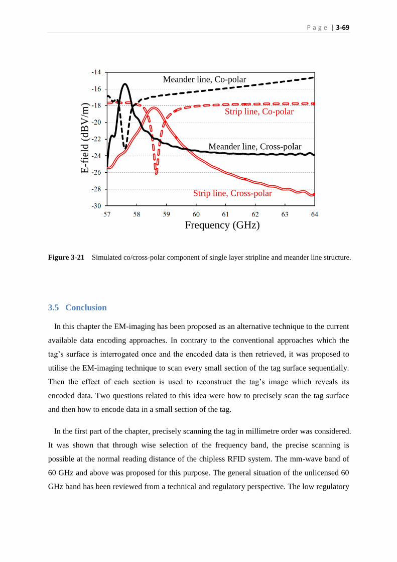
P a g e | 3-69
Figure 3-21 Simulated co/cross-polar component of single layer stripline and meander line structure.
3.5 Conclusion
In this chapter the EM-imaging has been proposed as an alternative technique to the current
available data encoding approaches. In contrary to the conventional approaches which the
tag’s surface is interrogated once and the encoded data is then retrieved, it was proposed to
utilise the EM-imaging technique to scan every small section of the tag surface sequentially.
Then the effect of each section is used to reconstruct the tag’s image which reveals its
encoded data. Two questions related to this idea were how to precisely scan the tag surface
and then how to encode data in a small section of the tag.
In the first part of the chapter, precisely scanning the tag in millimetre order was considered.
It was shown that through wise selection of the frequency band, the precise scanning is
possible at the normal reading distance of the chipless RFID system. The mm-wave band of
60 GHz and above was proposed for this purpose. The general situation of the unlicensed 60
GHz band has been reviewed from a technical and regulatory perspective. The low regulatory
E-f
ield
(d
BV
/m)
Frequency (GHz)
Meander line, Cross-polar
Strip line, Cross-polar
Meander line, Co-polar
Strip line, Co-polar
P a g e | 3-70
restrictions on the EIRP of this band have been highlighted that makes the band very suitable
for the proposed technique.
Earth imaging applications were considered in detail as the most important application of
the EM-imaging. The similarities and differences between earth imaging and the RFID
application have been considered. It was shown that the working basis of the reflected signal
level that is used for earth imaging is not appropriate for the RFID application due to the low
differences between reflection from conductive and non-conductive parts of the tag surface.
Then the idea of polarisation rotation through a narrow conductive strip has been proposed
that provides a new approach for EM-imaging of the tag. The strip line as an EM-polariser
has been tested through simulation results. Moreover, the effect of multiple strips and strips
with slightly different lengths were also considered. Those results are useful when the
measurement result of the strip line is considered in the next chapter.
The meander line as a transmission EM-polariser was considered. The multi-layer structure
of the meander lines was introduced and proposed as a reflective EM-polariser. The idea of
the multi-layer structure was rejected as it contradicts with the targeted tag cost of below 1¢
in the proposed application of the RFID systems. Then the meander line was re-designed on a
single layer structure without any ground plane. The meander line was simulated shows
sharper and higher cross-polar components than those for the strip line. The strip line and
meander line suggest a reliable approach to shape the tag’ surface in a way that the tag’s EM-
image would be unique. Therefore, it can be concluded that this chapter proves that the EM-
imaging of the tag is technically possible at 60 GHz mm-wave band and higher frequencies.
Moreover, it reveals a new way for shaping the tag surface for a unique EM-image purpose
through the printed EM-polarisers of the strip and meander lines.

P a g e | 4-71
Chapter 4 Practical data encoding EM-polariser
4.1 Introduction
In the preceding chapter, EM-imaging for chipless RFID tag has been introduced. It was
shown that through EM-imaging techniques, scanning of the small section of the tag surface
for data retrieving purpose is possible at the mm-wave frequency bands of 60 GHz and higher
frequency bands. Synthetic aperture radar technique as a powerful imaging approach was
suggested for RFID applications. The theories of EM-polarisers in the form of strip line and
meander line as practical and effective unit cells of data encoding device have been presented.
The working basis of these EM-polarisers has been presented in terms of their backscattered
cross-polar components. The simulation results confirmed the behaviour of the strip line and
meander line EM-polarisers as the basic structure for data encoding elements for the
proposed image based chipless RFID tag.
This chapter considers the fabrication process of the introduced polarisers. The polariser-
based tag is fabricated through an accurate photolithographic process on a dielectric structure.
Then the same tag structure, strip line and meander line polarisers, are printed with a SATO
inkjet printer that utilises conductive ink on a paper substrate. These two tag samples, through
different fabrication processes are carefully investigated by an electronic microscope
regarding their precise dimensions and shapes. It is shown that the printed sample suffers
severely from shape anomalies and changes in dimensions due to the printing resolution of
the SATO printer.
Then the fabricated tags, through a photolithographic process and printed tags with SATO
printer, are measured with real antennas to explore the actual performance of the designed
EM-polarisers. While the precisely fabricated tags show almost the same performance as
expected through simulation in Chapter 3, the printed samples lost all their resonance
behaviour. This is, however, in agreement with the simulation results of the multiple strip
lines with slightly different dimensions in Chapter 3. Then the possible data encoding
algorithm based on the measurement results for both tags prototype are discussed. Finally the
appropriate data encoding approaches suitable for the commercial use of the proposed image-
based technique, the printed tag, are considered. This step matures the proposed technique for
real world applications and it provides the appropriate ground for further research and work
in the rest of this thesis.

P a g e | 4-72
4.2 Tag fabrication
Two stripline and meander line EM-polarisers were designed in Chapter 3 and working on
the frequency band 57-64 GHz. These two designs and the related parameters are shown in
Figure 4-1. Designs are based on Taconic TLX-8 with εr =2.55 and thickness 0.127 mm. As
can be seen, the design accuracy is 0.05 mm. The total length of each polariser is around 1.6
mm. It is possible to fabricate a single polariser, however, the expected received power shall
be considered. As discussed in Section 3.3.1.1, the band 57-64 GHz is an ISM band with
generous permitted radiated power compared with other lower ISM bands. The maximum
EIRP at this frequency band is around 40 dBm in most the countries [31, 113] as presented
earlier in Table 3-2.
By assuming 10 dB average gain of the reader antenna, the input power to the transmitter
can be up to 30 dBm or equivalent to one watt. This provides noticeable reading range for
short range radio communication services including chipless RFID systems. In the
measurement process, the performance network analyser (PNA) Agilent E8361A is used due
to the lack of individual transmit and receive module on 60 GHz band at the Monash
Microwave, Antennas, RFID and Sensors (MMARS) laboratory. The maximum transmit
power of the PNA is limited to -5 dBm at the 60 GHz band meaning the total EIRP of 5 dBm
by assuming 10 dB antenna gain. To compensate this practical power limitation, more than
one polariser is used to provide the minimum reading range of 10~15 cm. Therefore, in all of
the measurement processes in this chapter onward, an array of five vertical polarisers are
used to create enough RCS at the reader side as shown in Figure 4-2.
Figure 4-1 (a) Strip line polariser, (b) Meander line polariser; all values are in mm.
1.60.2
1.6
0.15
0.1
0.35
(b)(a)

P a g e | 4-73
Figure 4-2 Fabricated EM-polarisers through photolithographic process.
4.2.1 Photolithographic fabrication process
The designed polarisers, strip line and meander line, are fabricated through a
photolithographic process. The conductive part is the annealed copper and dielectric is the
Taconic TLX-8 with εr = 2.55 and thickness 0.127 mm. The photographs of these two
polarisers are shown in Figure 4-2.
4.2.2 Printing process
It was thoroughly discussed in previous chapters that any suggestion for chipless RFID
systems shall be based on the printed tag structure. Otherwise, obtained results based on
perfect materials and costly fabrication processes does not guarantee the successful
performance of any proposed approach at the commercial stage. This is the most significant
phase of the research field in the chipless RFID systems. Many techniques and ideas have
been proposed in this area of research. Some show satisfactory achievement at early stage of
the research. However, no further deployment of them has been seen in the market only due
to a significant performance reduction based on the printed tag structure.
To evaluate performance of the proposed image-based approach for the chipless RFID
applications, the polariser-based tag is printed by a SATO GL4e industrial thermal silver ink
based printer with a 600 dpi resolution [114]. SATO uses aluminum-based ink as the
conductor and normal paper is utilised as the substrate.
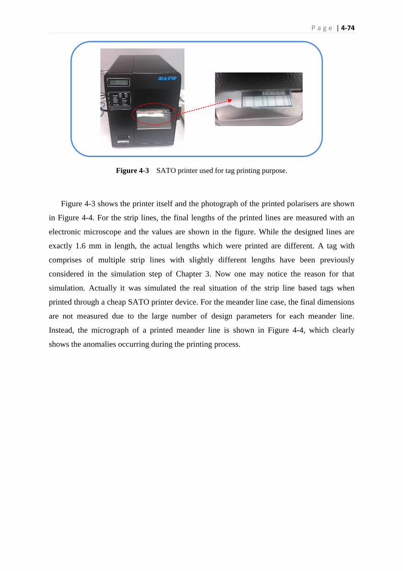
P a g e | 4-74
Figure 4-3 SATO printer used for tag printing purpose.
Figure 4-3 shows the printer itself and the photograph of the printed polarisers are shown
in Figure 4-4. For the strip lines, the final lengths of the printed lines are measured with an
electronic microscope and the values are shown in the figure. While the designed lines are
exactly 1.6 mm in length, the actual lengths which were printed are different. A tag with
comprises of multiple strip lines with slightly different lengths have been previously
considered in the simulation step of Chapter 3. Now one may notice the reason for that
simulation. Actually it was simulated the real situation of the strip line based tags when
printed through a cheap SATO printer device. For the meander line case, the final dimensions
are not measured due to the large number of design parameters for each meander line.
Instead, the micrograph of a printed meander line is shown in Figure 4-4, which clearly
shows the anomalies occurring during the printing process.
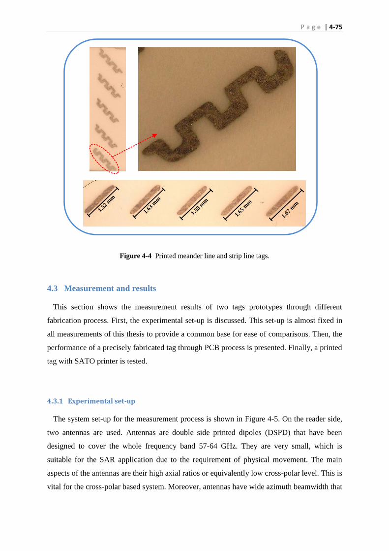
P a g e | 4-75
Figure 4-4 Printed meander line and strip line tags.
4.3 Measurement and results
This section shows the measurement results of two tags prototypes through different
fabrication process. First, the experimental set-up is discussed. This set-up is almost fixed in
all measurements of this thesis to provide a common base for ease of comparisons. Then, the
performance of a precisely fabricated tag through PCB process is presented. Finally, a printed
tag with SATO printer is tested.
4.3.1 Experimental set-up
The system set-up for the measurement process is shown in Figure 4-5. On the reader side,
two antennas are used. Antennas are double side printed dipoles (DSPD) that have been
designed to cover the whole frequency band 57-64 GHz. They are very small, which is
suitable for the SAR application due to the requirement of physical movement. The main
aspects of the antennas are their high axial ratios or equivalently low cross-polar level. This is
vital for the cross-polar based system. Moreover, antennas have wide azimuth beamwidth that
1.52
mm
1.65
mm
1.63
mm
1.58
mm
1.67
mm
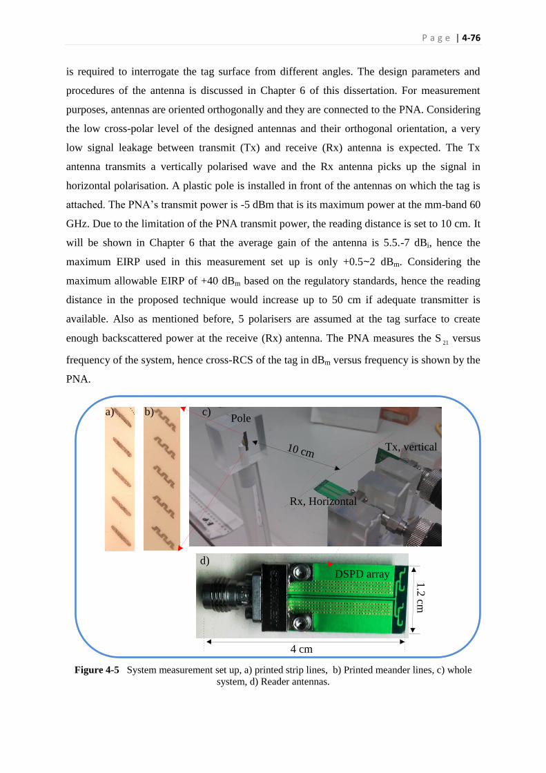
P a g e | 4-76
is required to interrogate the tag surface from different angles. The design parameters and
procedures of the antenna is discussed in Chapter 6 of this dissertation. For measurement
purposes, antennas are oriented orthogonally and they are connected to the PNA. Considering
the low cross-polar level of the designed antennas and their orthogonal orientation, a very
low signal leakage between transmit (Tx) and receive (Rx) antenna is expected. The Tx
antenna transmits a vertically polarised wave and the Rx antenna picks up the signal in
horizontal polarisation. A plastic pole is installed in front of the antennas on which the tag is
attached. The PNA’s transmit power is -5 dBm that is its maximum power at the mm-band 60
GHz. Due to the limitation of the PNA transmit power, the reading distance is set to 10 cm. It
will be shown in Chapter 6 that the average gain of the antenna is 5.5.-7 dBi, hence the
maximum EIRP used in this measurement set up is only +0.5~2 dBm. Considering the
maximum allowable EIRP of +40 dBm based on the regulatory standards, hence the reading
distance in the proposed technique would increase up to 50 cm if adequate transmitter is
available. Also as mentioned before, 5 polarisers are assumed at the tag surface to create
enough backscattered power at the receive (Rx) antenna. The PNA measures the S21
versus
frequency of the system, hence cross-RCS of the tag in dBm versus frequency is shown by the
PNA.
Figure 4-5 System measurement set up, a) printed strip lines, b) Printed meander lines, c) whole
system, d) Reader antennas.
10 cm Tx, vertical
Rx, Horizontal
Pole
DSPD array
4 cm
1.2
cm
a) b) c)
d)

P a g e | 4-77
4.3.2 Precise tag results
The fabricated tags through the photolithographic process that have been introduced in
Section 4.2.1 and shown in Figure 4-2, are attached to the pole for measurement purposes.
The tag surface is interrogated by a vertically polarised antenna and the receiver at the reader
measures the backscattered signals with a horizontal polarised antenna. The S21 in dB versus
frequency is shown in Figure 4-6. The red dashed line in Figure 4-6 shows the S21 when no
tag is attached to the pole in front of the reader antennas. The signal level is below -65 dBm.
This presents the amount of signal leakage and mutual coupling between the two
orthogonally polarised antennas as well as the effect of a plastic pole. The very low signal
level is not unexpected as antennas are oriented orthogonally and each antenna has a low
cross-polar level.
Attaching a tag comprises of five precisely fabricated strip lines through a
photolithographic process significantly increases the received power level by at least 15 dB
as shown in Figure 4-6. The signal level would be up to 30 dB higher at the resonance
frequency 60.2 GHz. This result clearly verifies the strip line as an effective EM-polariser.
Comparing the measured results with the simulation outcomes in Chapter 3 confirms that the
resonance bandwidth of the tag has been increased in the real scenario. The broader
resonance bandwidth is important as it challenges the resonance-based idea for data
encoding. Even though the tag has been fabricated through an accurate and expensive process
by utilising high quality copper and dielectric substrate, the actual Q factor of the element is
lower than that of expected in simulation.
Interrogating five precisely fabricated meander lines by the vertical oriented antenna,
creates a backscattered signal which includes a high orthogonal component. This cross-polar
component is easily picked up by the receive antenna oriented horizontally. Similar to the
strip lines case, the received signal level is almost 18 dB higher than that of the “no tag” case.
At the resonance frequency 60.5 GHz, the signal level is 30 dB stronger. The meander lines
show a higher Q factor than that of the strip lines. However, their resonance bandwidth is
again increased with respect to the simulation results shown in Chapter 3.
In summary, it can be concluded that the strip line and meander line act as an effective EM-
polariser at the designed band 57-64 GHz. They both suffer Q factor reduction due to the
non-ideal behaviour of elements in a real scenario, specifically at the mm-band 60 GHz.
While, their resonance behaviour are clearly noticeable and suggest an approach for the data
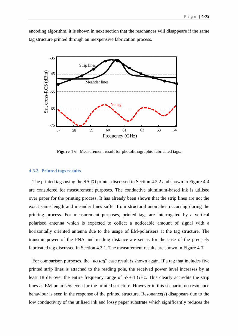
P a g e | 4-78
encoding algorithm, it is shown in next section that the resonances will disappeare if the same
tag structure printed through an inexpensive fabrication process.
Figure 4-6 Measurement result for photolithographic fabricated tags.
4.3.3 Printed tags results
The printed tags using the SATO printer discussed in Section 4.2.2 and shown in Figure 4-4
are considered for measurement purposes. The conductive aluminum-based ink is utilised
over paper for the printing process. It has already been shown that the strip lines are not the
exact same length and meander lines suffer from structural anomalies occurring during the
printing process. For measurement purposes, printed tags are interrogated by a vertical
polarised antenna which is expected to collect a noticeable amount of signal with a
horizontally oriented antenna due to the usage of EM-polarisers at the tag structure. The
transmit power of the PNA and reading distance are set as for the case of the precisely
fabricated tag discussed in Section 4.3.1. The measurement results are shown in Figure 4-7.
For comparison purposes, the “no tag” case result is shown again. If a tag that includes five
printed strip lines is attached to the reading pole, the received power level increases by at
least 18 dB over the entire frequency range of 57-64 GHz. This clearly accredits the strip
lines as EM-polarisers even for the printed structure. However in this scenario, no resonance
behaviour is seen in the response of the printed structure. Resonance(s) disappears due to the
low conductivity of the utilised ink and lossy paper substrate which significantly reduces the
-75
-65
-55
-45
-35
59.999 60.01335 60.0277 60.04205 60.0564 60.07075 60.0851 60.09945
Frequency (GHz)
S2
1, cr
oss
-RC
S (
dB
m)
57 58 59 60 61 62 63 64
-75
-65
-55
-45
-35
No tag
Strip lines
Meander lines
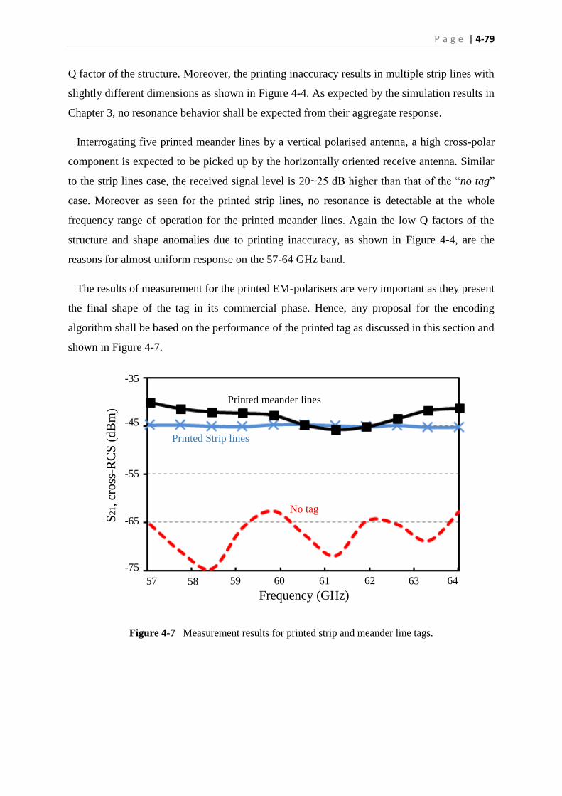
P a g e | 4-79
Q factor of the structure. Moreover, the printing inaccuracy results in multiple strip lines with
slightly different dimensions as shown in Figure 4-4. As expected by the simulation results in
Chapter 3, no resonance behavior shall be expected from their aggregate response.
Interrogating five printed meander lines by a vertical polarised antenna, a high cross-polar
component is expected to be picked up by the horizontally oriented receive antenna. Similar
to the strip lines case, the received signal level is 20~25 dB higher than that of the “no tag”
case. Moreover as seen for the printed strip lines, no resonance is detectable at the whole
frequency range of operation for the printed meander lines. Again the low Q factors of the
structure and shape anomalies due to printing inaccuracy, as shown in Figure 4-4, are the
reasons for almost uniform response on the 57-64 GHz band.
The results of measurement for the printed EM-polarisers are very important as they present
the final shape of the tag in its commercial phase. Hence, any proposal for the encoding
algorithm shall be based on the performance of the printed tag as discussed in this section and
shown in Figure 4-7.
Figure 4-7 Measurement results for printed strip and meander line tags.
Frequency (GHz)
S2
1,
cro
ss-R
CS
(d
Bm
)
57 58 59 60 61 62 63 64
-75
-65
-55
-45
-35
No tag
Printed Strip lines
Printed meander lines

P a g e | 4-80
4.3.4 Cross-polar RCS
The results of measurement for the PCB and printed EM-polarisers shall be considered very
carefully as they presents two critical aspects of the research. These two factors can be
summarized as follow:
i) Proof of polariser performance. The results shown in Figure 4-6 and Figure 4-7 confirm
the performance of the strip and meander lines as effective polarisers. All measurements were
performed in the laboratory environment and not in an anechoic chamber. Moreover, no
calibration or reference tag has been utilised. These considerations endorse the suggested
stripline and meander line as suitable, low cost, compact and effective polarisers in the mm-
band, which validates the data encoding method in the suggested image-based chipless RFID
system.
ii) Rejection of resonance-based encoding approaches. Extensive system tunings have been
considered to calibrate the SATO printer for a most accurate printing result. All the printed
tag structures show almost the same results as shown in Figure 4-7. It appears that the low
cost printing technology is not mature enough for the demanded accuracy in RFID
applications. This suggests that any resonance-based approach for data encoding faces huge
limitations at the commercial phase of the system implementation. High resolution printing
methods in the order of 10-20 µm are too expensive and slow processes, laser printing for
example.
Irrespective of lost resonant at the backscattered signal due to the printing inaccuracy and
low quality of materials in the tag structure, the measured high cross-polar signal can be
utilised for a cross-polar RCS based data encoding algorithm. This new basis is used in the
proposed theory of the EM-image chipless RFID system. Therefore, in the proposed image-
based technique, the system does not rely on resonance detection hence, is robust towards the
printing inaccuracy and therefore the low cost printers are still viable methods.
4.4 Discussion on data encoding method
4.4.1 Pros of EM-polarisers
The measurement results based on the precise fabricated tag and the printed tag discussed
in Section 4.3 have revealed the potential advantages and limitations of the proposed strip

P a g e | 4-81
line and meander line as EM-polarisers. The most advantages of the proposed polariser-based
tag are:
i) Small size. The size of the polarisers is less than 0.5 × 2 mm2 which makes them very
suitable for data encoding in the RFID applications. The tiny size of the polariser, due to the
simple structure of the component and the mm-wave band of operation, elevates the chance
of high data encoding capacity in the proposed technique.
ii) Cross-polar working basis. The interrogation signal by the reader is converted to the
orthogonal polarised backscattered signal due to the EM-polarisers on the tag surface. This
working basis provides huge advantages for the proposed system with elimination of noises
and the interferences from different sources. System robustness towards multipath
interference and clutter and no requirement for system calibration are the unique advantages
of this cross-polar working basis.
iii) Adequate performance with the printed tag. The proposed simple tag structure
guarantees its adequate performance even on a fully printed tag as confirmed in the
measurement step in Section 4.3. Suffering from shape anomalies and inaccurate dimensions,
the polariser-based printed tag performs well for creation of a high cross-polar component at
the backscattered direction. This assures the successful implementation of the proposed
technique for real applications.
The only limitation of the proposed technique is the lack of resonances at the backscattered
signal. The measurements showed that it would not be practical to expect multiple resonances
from a printed tag structure. The printing inaccuracy negates the idea of recognising the tag
by its frequency signature in co- or cross-polar responses. Although working on lower
frequencies may reduce the effect of printing inaccuracy, the limited spectrum available on
lower frequencies and the very low Q factor of the printed resonators, still affect the final
encoding capacity of the system [79]. Although this limitation originated from immature
printing technologies for low cost items, it is the duty of the proposed technique to suggest a
suitable data encoding approach addressing the capacities of the current printing
technologies. Otherwise, any solution based on the very accurate and costly tag fabrication
process finds no place in the RFID market.

P a g e | 4-82
4.4.2 On/off image-based data encoding algorithm
The idea of EM-imaging has already been introduced in Chapter 3. It was stated that in the
imaging technique, every small section of the tag surface is sequentially scanned by the
reader and its related encoded data is retrieved, see Figure 3-1. Now, the way that data can be
encoded in every small section of the tag surface is discussed. It has already been shown that
a small size EM-polariser can create strong enough cross-polar components in the backscatter
direction, which can be easily detected by the reader array antenna. One may suggest using
these polarisers on the tag surface as the data encoding elements. In this approach, the tag
surface comprises a matrix of m × n pixels as shown in Figure 4-8. Every pixel which is as
small as 2 × 2 mm2 may include one polariser. When the reader scans a particular pixel, the
presence or absence of the polariser results in a completely different received signal level at
the cross-polar direction that acts as a binary data; existence of the polariser as “1” and no
polariser as “0”, for example. Therefore, binary digit data encoding approach is implemented
by the polarisers. No resonance is to be found from the backscattered signal for data
encoding. Creation of such precise scanning on the tag surface in millimetre order in the real
scenario is a matter of question though. In Chapter 7, the EM-imaging theory is reviewed in
detail and it is shown that this scanning precession of the tag surface is possible at a suitable
frequency range and with appropriate approaches. The final result shown in Chapter 7 with
five millimetre scanning precision proves the validity of this suggestion.
At this stage, the general system structure for the first phase of the proposed image-based
theory can be figuratively shown as in Figure 4-8. The system requires the reader’s physical
movement around the tag to create a synthetic aperture. The length of this aperture governs
the horizontal resolution on the tag surface, known as cross-range or azimuth resolution. It is
discussed in Chapter 7 that a 20~30 cm synthetic aperture size would be enough to create 2~5
mm cross-range resolution on the tag surface at the reading range of 10~20 cm. The ability of
the system to provide precise vertical resolution, known as range resolution, depends on the
type and frequency band of the transmit signal. At the aforementioned reading range, the
range resolution of 2~10 mm is also feasible with a high rate chirp signal covering a
significant bandwidth. This issue is also discussed in more detail in Chapter 7. The
requirement of the physical movement of the reader can be replaced by a linear array of
radiators on a MIMO working basis. This enhances the reading time and elevates the
potentials of the proposed theory. The detail of this new MIMO-based reader is introduced in
Chapter 8.
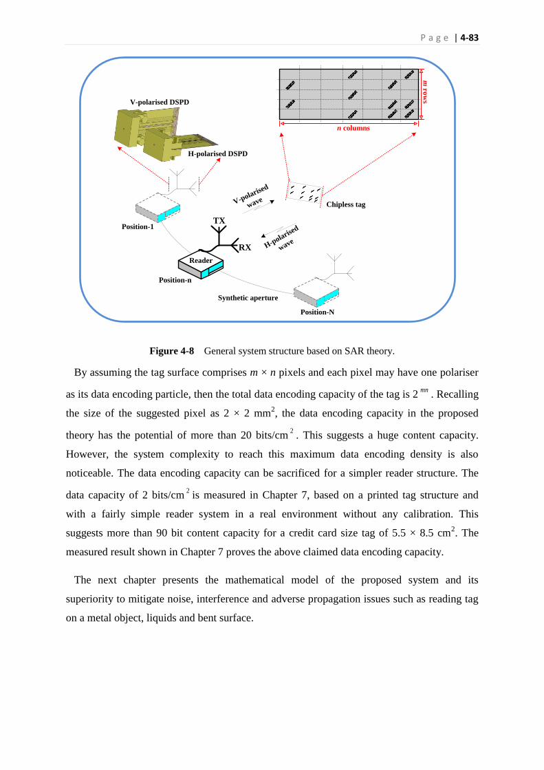
P a g e | 4-83
Figure 4-8 General system structure based on SAR theory.
By assuming the tag surface comprises m × n pixels and each pixel may have one polariser
as its data encoding particle, then the total data encoding capacity of the tag is 2mn
. Recalling
the size of the suggested pixel as 2 × 2 mm2, the data encoding capacity in the proposed
theory has the potential of more than 20 bits/cm2
. This suggests a huge content capacity.
However, the system complexity to reach this maximum data encoding density is also
noticeable. The data encoding capacity can be sacrificed for a simpler reader structure. The
data capacity of 2 bits/cm2
is measured in Chapter 7, based on a printed tag structure and
with a fairly simple reader system in a real environment without any calibration. This
suggests more than 90 bit content capacity for a credit card size tag of 5.5 × 8.5 cm2. The
measured result shown in Chapter 7 proves the above claimed data encoding capacity.
The next chapter presents the mathematical model of the proposed system and its
superiority to mitigate noise, interference and adverse propagation issues such as reading tag
on a metal object, liquids and bent surface.
RX
Synthetic aperture
V-polarised
waveChipless tag
TX
H-polarised
wave
V-polarised DSPD
H-polarised DSPD
Reader
Position-1
Position-n
Position-N
m ro
ws
n columns

P a g e | 4-84
4.5 Conclusion
This chapter has considered the fabrication process of the designed polarisers. The strip line
and meander line-based tags were fabricated through two different technologies. First, the
EM-polariser based tags were made through an accurate and costly photolithographic process.
Each tag included five polarisers oriented vertically. Then the same designs were printed with
a SATO printer. The SATO printer uses conductive aluminium ink for printing on normal
paper. Two samples of the tags have been accurately examined with an electronic microscope.
The printed meander lines showed considerable shape anomalies. Printed strip lines were also
measured to find their final lengths. It was found that five strip lines had different lengths
than the designed dimensions.
Both PCB and printed tags for each case of the strip line and meander line have been
measured in a real scenario. Two sets of double sided printed dipole arrays were used at the
reader side. They were oriented orthogonally as transmit and receive antennas. The array
antennas were connected to the PNA and various types of tags were placed in front of the
antennas. The measurement process was carried out in the laboratory environment. Precise
fabricated PCB tags for both a strip line and meander line polarisers showed similar results,
as expected by the simulation in Chapter 3. Their resonance bandwidths, however, were
broadened due to the non-ideal behaviour of the copper and substrate and other
environmental and propagation issues at the measurement process. On the other hand, printed
tag structures did not exhibit any resonance in their backscattered signal. However, they were
showing significant cross-polar components. Non-resonance behaviour was linked to their
shape anomalies and also related to the very low Q factor of the printed polarisers.
The results of printed tags have been considered as the significant performance of the
proposed EM-polarisers for real world application in RFID systems. Then the data encoding
algorithm was proposed based on this minimum criterion. As the resonance frequency
signature based approach for the printed tag was failed, an alternative on/off image-based
technique was suggested for the data encoding algorithm. In this approach, the presence or
absence of an individual polariser on each small pixel of the tag surface acts as binary data “1”
or “0”. When the reader precisely scans the tag surface, it receives a completely different
signal level based on the existence of polarisers. The maximum theoretical content capacity
of the system based on this approach has been presented next. It has been addressed that to
reduce the system complexity, the data encoding capacity is sacrificed for a simpler system

P a g e | 4-85
structure. Finally, the claimed data encoding capacity based on a fully printable tag structure
and a simple reader system with low frequency bandwidth, is still much higher than that
already shown by other competitors in the chipless RFID systems.

P a g e | 5-86
Chapter 5 Printed EM-polariser performance
5.1 Introduction
Electromagnetic (EM) polarisers have been introduced in Chapter 3. The edge diffraction of
the polariser and the antenna mode RCS of the polariser result in significant cross-polar
components in the backscattered direction. This is the basis for the cross-polar EM-image
based chipless RFID system.
Next the proposed EM-polarisers were fabricated through a photolithographic process and
printed with a SATO GL4e industrial thermal silver ink based printer with 600 dpi resolution.
Both prototype tags were tested in the laboratory environment. Both tags through two
different fabrication processes showed prominent de-polarisation behaviour. While the
impinging signal was linearly polarised, the reflected signals showed high cross-polar
components. However, for the printed tag structure, no resonances were detectable on the
received signal, due to the printing errors of the SATO printing and low quality of the
materials. Therefore, it has been established that SATO printed tag still provide adequate
cross-polar RCS, while is useful for EM-image based binary data encoding. This result has
been discussed in details in Chapter 4.
In this chapter, the robustness of the EM-polarisers toward unwanted reflections and
multipath interferences is considered. This system robustness is one of the most important
salient aspects of the proposed EM-polarisers. First, the equivalent system model is
introduced to ease the network analysis of the proposed EM-polariser based system. The
effectiveness of the system for unwanted reflections is proved mathematically. Then different
measurement scenarios are considered to investigate the system robustness in various
scenarios. It is shown through measurement that the EM-polarisers can effectively create
cross-polar RCS components in the backscattered direction on which the receiver easily
detects the presence of the EM-polarisers. The effect of reflections from other objects and
multipath interferences are also considered in the measurement process and the system
robustness is proved. This finding suggests huge advantages of the EM-polariser based
system for industrial environments. Moreover, the polariser-based tag is shown to be very
efficient for tagging of highly reflective items; water bottles or metallic cans for example.
The bending effect of the tag conformal to various types of objects, on its cross-polar
performance, is also considered in this chapter.

P a g e | 5-87
The robustness of the proposed tag for harsh industrial environments is presented at the end
of this chapter. The cross-polar based system effectively decodes the tag’s data with
reasonable reader complexity. No complex system calibration process is needed for the
proposed system structure. All the measurements and conclusions are based on the
performance of a fully printed tag structure in a laboratory environment.
5.2 System analytical model
To explore the potential of the cross-polar based system, the equivalent system network is
introduced. This enables the mathematical analysis of the tag response and realization of the
system robustness towards reflection and multipath interferences. Moreover, in the theoretical
evaluation of the proposed technique, the drawbacks and limitations of the co-polar based
system as the working basis of many current techniques in the chipless RFID systems, is
explored. It should be noted that the frequency, time and, most of hybrid domain based
chipless RFID tags works on the co-polar backscattered signal hence susceptible to noise and
interferences. To alleviate the situation, rigorous calibration is required to extract data.
As previously discussed, the tag is interrogated with a linearly polarised signal; vertical
polarisation, for example. The backscattered response is picked up by the receiver in the
orthogonal direction; horizontal polarisation for example. The RCS of the tag relates to many
parameters including the frequency and polarisation of the impinged signal, the aspect angle
of the tag and its physical size and structure [80]. For a certain frequency and aspect angle,
the RCS behaviour depends on the interrogation signal’s polarisation by [115]:
vv vh
hv hh
(7.0)
In (7.0), σ represents the tag’s scattering behavior. Each matrix element, σij, shows the tag
response in a j polarisation scheme while interrogated by an i polarised signal. For simplicity,
the vertical (v) and horizontal (h) polarisations are assumed in this work while (7.0) is valid
for any orthogonal polarisations.
Evaluation of the proposed technique requires a circuit model. The suggested model shall
include all the elements of the technique. One possible model for the chipless RFID system
was introduced by [116]. This model includes the effect of Tx and Rx antennas, the response

P a g e | 5-88
of the chipless tag and the equivalent response of all interfering objects surrounding the tag as
shown in Figure 5-1. Each block in the model shows a specific section of the communication
link. As two vertical and horizontal polarisations were assumed in the model, then each box
has a 2 × 2 S-parameters matrix which characterises its behavior in co- and cross-polar
directions.
In Figure 5-1, the transceiver module on the reader side is denoted by block M. The source
is assumed to send a pure V-polarised signal and the receiver is expected to collect the
backscattered signal only in a H-polarisation direction. However, due to the non-ideal
behaviour of the elements involved in the link, there is the possibility of errors in the tag
detection process. The model is intended to find those errors and mathematically evaluates
their weights in the final performance of the system. The Tx antenna and its connected cable
and connectors are symbolised by block T or the transmit path. Likewise, the receiver antenna
and cables are shown through box R or receive path. The coupling among Tx and Rx
antennas always exist. To show the effect of coupling, block D is considered in the model.
Existence of the tag in front of the antennas causes reflection of energy towards the reader’s
receive antenna. This is the intended reflection which carries the tag information. This link is
shown by block C in Figure 5-1. Apart from direct coupling and reflection by the tag, there is
the possibility of receiving the signal through the reflections by other objects around the tag.
This includes everything located in the reader’s reading zone. The item to which the tag is
attached, such as the walls, floor and ceiling, are examples. Normally these reflections are
undesirable phenomena and known as interference. Their effects significantly contribute to
system performance, and therefore, shall be considered in the schematic block diagram. The
box I represents the effect of all those interfering factors so it covers all unwanted reflections,
multipath interferences, and clutter.
The S-parameter matrix of the reader, M, can be related to the S-matrix of other blocks by:
M TDR TCR TIR (7.1)
In the above equation, TDR shows the amount of coupling or direct leakage between transmit
and receive antennas. This part is independent of the effect of the tag or other objects.
Therefore, leakage, L, can be directly measured when there is nothing in front of the
antennas.
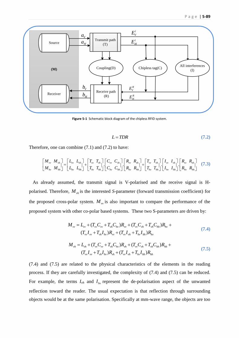
P a g e | 5-89
Figure 5-1 Schematic block diagram of the chipless RFID system.
L TDR (7.2)
Therefore, one can combine (7.1) and (7.2) to have:
. . . .vv vh vv vh vv vh vv vh vv vh vv vh vv vh vv vh
hv hh hv hh hv hh hv hh hv hh hv hh hv hh hv hh
M M L L T T C C R R T T I I R R
M M L L T T C C R R T T I I R R
(7.3)
As already assumed, the transmit signal is V-polarised and the receive signal is H-
polarised. Therefore, vhM is the interested S-parameter (forward transmission coefficient) for
the proposed cross-polar system. vvM is also important to compare the performance of the
proposed system with other co-polar based systems. These two S-parameters are driven by:
( ) ( )
( ) ( )
vv vv vv vv vh hv vv vv vh vh hh hv
vv vv vh hv vv vv vh hv hh hv
M L T C T C R T C T C R
T I T I R T I T I R
(7.4)
( ) ( )
( ) ( )
vh vh vv vv vh hv vh vv vh vh hh hh
vv vv vh hv vh vv vh hv hh hh
M L T C T C R T C T C R
T I T I R T I T I R
(7.5)
(7.4) and (7.5) are related to the physical characteristics of the elements in the reading
process. If they are carefully investigated, the complexity of (7.4) and (7.5) can be reduced.
For example, the terms Ivh and hvI represent the de-polarisation aspect of the unwanted
reflection toward the reader. The usual expectation is that reflection through surrounding
objects would be at the same polarisation. Specifically at mm-wave range, the objects are too
(M)
Source
Receiver
Transmit path
(T)
Va
Ha
Vb
HbReceive path
(R)
Coupling(D) Chipless tag(C)All interferences
(I)
i
VE
i
HE
R
VE
R
HE

P a g e | 5-90
big to create a de-polarised signal due to the diffraction effect. Multipath interferences and
clutter also show no de-polarisation behaviour, hence the vhI and hvI can be correctly assumed
to be zero. Tij and Rij on which i j , are related to the antenna polarisation or the antenna’s
CPL. As is shown in the next chapter, the designed array antenna for the proposed image-
based chipless RFID system has a high CPL of more than 20 dB. Moreover, the PNA Agilent
E8361A has a high quality cable and connectors with very high isolation in the order of
80 ~100 dB [117]. This means that the value of ijT and
ijR are less than 0.01 and again can be
correctly neglected.
By applying the aforementioned simplifications, (7.4) and (7.5) become:
( )vv vv vv vv vv vvM L T R C I (7.6)
vh vh vv vh hhM L T C R (7.7)
In the above formulas, ijL refers to the leakage between Tx and Rx modules of the reader
whether in co- or cross-polar directions. The following statements are related to the leakage:
Leakage measurement. In an empty environment, leakage (ijL ) can be directly
measured. The value of ijL depends on the internal characteristics of the designed
antenna and is also related to the physical distance between the Tx and Rx antennas.
Once ijL is measured, it does not change with varying the reading scene.
Significance of leakage. The leakage for the co-polar case would be much higher than
that of the cross-polar scenario vvL > vhL . If the co-polar leakage ( vvL ) is not
controlled well, it may significantly affect the final system performance.
Leakage control. The leakage control for the co-polar, vvL , is much more complex
than that for the cross-polar, vhL . This is because in the co-polar case, both transmit
and receive antennas are on the same polarisation scheme and, hence, they are more
likely to interfere to each other.
Therefore, it can be concluded that the leakage in the cross-polar case is much less than that
of the co-polar and, hence, it has less effect on the reading process. Moreover, the leakage

P a g e | 5-91
control is also much easier in the cross-polar scenario. This is one of the most significant
advantages of the cross-polar scenario over the co-polar working basis.
In (7.7) which relates to the cross-polar scenario, the term vv vh hhT C R refers to the mixed
effects of the Tx, Rx and the tag. To accurately determine the coupling coefficient .vv hhT R due
to the filtering effect of the transmitter and receiver antennas, it is required to utilise a
reference tag with known scattering behaviour. Therefore, the tag’s scattering term ( vhC ) can
be easily found as:
ref
vh vhvv hh ref
vh
M LT R
C
(7.7)
refvh vhvh vhref
vh vh
M LC C
M L
(7.8)
where vhL is a fixed value based on the Tx and Rx antennas distance and ref
vhM is the measured
scattering parameter of a reference tag.
One may suggest performing the same approach for the co-polar scenario. However, as it is
clear from (7.6) an extra term vvI also exists for the co-polar case. The vvI counts the effect
of reflections from surrounding objects around the tag. As the tag size is very small compared
to other surrounding objects, then the vvI is much larger than the vvC in (7.6). This means that
it is not possible to extract the tag response without the information about its surrounding
objects. Indeed, it is required to first calibrate the system based on a specific orientation of
objects in the reading zone and then detect the response of the tag by subtracting two
measurement results. Although with this calibration process, the tag reading would be
possible in the co-polar scenario, the approach is very sensitive to any changes in the
surrounding objects orientations or tag movement. This means that if the tag moves in the
reading zone or if one object around the tag changes its place or aspect angle, then it is
required to calibrate the system again. On the contrary, the cross-polar scenario is not
dependent on the surrounding objects and no information is required. This is a very
significant aspect of the cross-polar working basis, as the system is working well in an
unknown reading zone only with a unique calibration set up. This aspect of the proposed
cross-polar system is shown in a practical scenario in the following sections.

P a g e | 5-92
5.3 Effects of multipath interference and clutter
The strip line and meander line were measured in Chapter 4 with respect to their de-
polarisation aspects. Both precisely fabricated PCB tags and the SATO printed tags were able
to provide high cross-polar components in the backscattered direction, hence, acting
effectively as EM-polarisers. Moreover, it was also mathematically shown in Section 5.2 that
the proposed cross-polar technique suggests high robustness towards multipath interference
as its dominant feature with respect to the co-polar working basis. This aspect of the proposed
approach is verified through a real measurement process in this section.
The measurement set up is similar to what was explained in Chapter 4 and shown in Figure
4-5. The reading distance, transmit output power and all other parameters are the same for
making the comparison possible. Exploring the effect of multipath and reflection
interferences on the reading process, the measurement is accomplished in the lab
environment and not in an anechoic chamber. Moreover, a harsh and severe multipath
situation is implemented by using some randomly selected highly reflective objects. Three
horn antennas are directed toward the reader antennas. A large printed circuit board with 35 ×
45 cm2 is also placed in front of the reader. This reading arrangement considers the most
sever interference situation for the system reading process. The Tx and Rx antennas together
with the highly reflective items are shown in Figure 5-2.
To simulate the high clutter situation, a big copper plate is attached to the reading pole. The
size of the plate is very large compared with the reader antennas and the reading distance. It
is 20 × 25 cm2. This highly reflective barrier causes a challenging situation for many
traditional chipless RFID systems. The reflection from this plate ( vvI ) is much higher than
that of the tag ( vvC ) as discussed in the previous section. Therefore, the detection of the tag
would be impossible unless the effect of high reflection is deleted through a calibration
process. The calibration however, is sensitive to any changes in the orientation of the objects
around the tag and the tag movement. This scenario is shown in Figure 5-3.
These two scenarios are considered in the measurement process and the results are shown
in Figure 5-4. For comparison purposes, two results from a normal situation are also repeated
in Figure 5-4. They are a “no tag” case and a printed meander line tag in a normal situation
from Chapter 4, Figure 4-7. As the graphs in Figure 5-4 show, the effect of multipath
interference and clutter on the received signal are almost negligible and very similar to the

P a g e | 5-93
Figure 5-2 Severe multipath interference scenario.
Figure 5-3 High clutter situation for the tag reading process.
Tx and Rx antennas
Reading pole
Tx and Rx antennas
Big metal plate
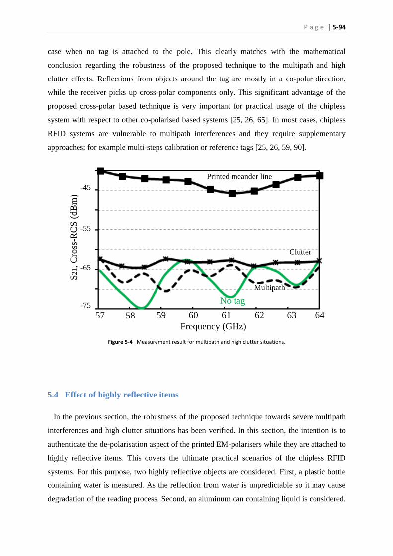
P a g e | 5-94
case when no tag is attached to the pole. This clearly matches with the mathematical
conclusion regarding the robustness of the proposed technique to the multipath and high
clutter effects. Reflections from objects around the tag are mostly in a co-polar direction,
while the receiver picks up cross-polar components only. This significant advantage of the
proposed cross-polar based technique is very important for practical usage of the chipless
system with respect to other co-polarised based systems [25, 26, 65]. In most cases, chipless
RFID systems are vulnerable to multipath interferences and they require supplementary
approaches; for example multi-steps calibration or reference tags [25, 26, 59, 90].
Figure 5-4 Measurement result for multipath and high clutter situations.
5.4 Effect of highly reflective items
In the previous section, the robustness of the proposed technique towards severe multipath
interferences and high clutter situations has been verified. In this section, the intention is to
authenticate the de-polarisation aspect of the printed EM-polarisers while they are attached to
highly reflective items. This covers the ultimate practical scenarios of the chipless RFID
systems. For this purpose, two highly reflective objects are considered. First, a plastic bottle
containing water is measured. As the reflection from water is unpredictable so it may cause
degradation of the reading process. Second, an aluminum can containing liquid is considered.
Frequency (GHz)
S2
1,
Cro
ss-R
CS
(dB
m)
57 58 59 60 61 62 63 64-75
-65
-55
-45
Printed meander line
Clutter
No tag
Multipath

P a g e | 5-95
The high reflection from the conductive body of the container as well as the bending effect
affects the measured results. These two scenarios are discussed in this section.
5.4.1 Liquid container
A normal plastic bottle of water is considered, to evaluate system performance. The tag is a
single-layer structure consisting of printed polarisers on paper. The object and attached
printed tag are shown in Figure 5-5. The tag consists of normal printed meander lines as
highlighted in the picture. The reading distance is set from the tag surface to the reader’s
antennas.
The measurement results for the water bottle are shown in Figure 5-6. For comparison
purposes, the measured results of the “no tag” case are also shown in Figure 5-6. As the
graphs show, when no tag is placed in front of the antennas, the received signal level is below
-65 dBm. Having a water bottle that is comparatively very large with no attached tag has a
minor effect on the cross-polar component of the received signal. A maximum of 5 dB
increase is experienced in this case. However, if the same water bottle includes a tiny printed
tag as shown in Figure 5-5, then the received signal is significantly elevated. The received
signal level from the tag attached to the water bottle has 12 dB more compared to that when
the water bottle has no attached tag. This margin provides a reliable reading scenario of the
liquid containers. Therefore, it can be concluded that the system has satisfactory performance
when attaching to the liquid container. It is important to mention that no calibration process
to cancel out the surrounding effect is required to obtain the graphs of Figure 5-6. If the
calibration process mentioned in the mathematical step at Section 5.2 is utilised, then a much
clearer signal level is expected to be seen on the graphs for the cross-polar components of the
received signals from the tag.
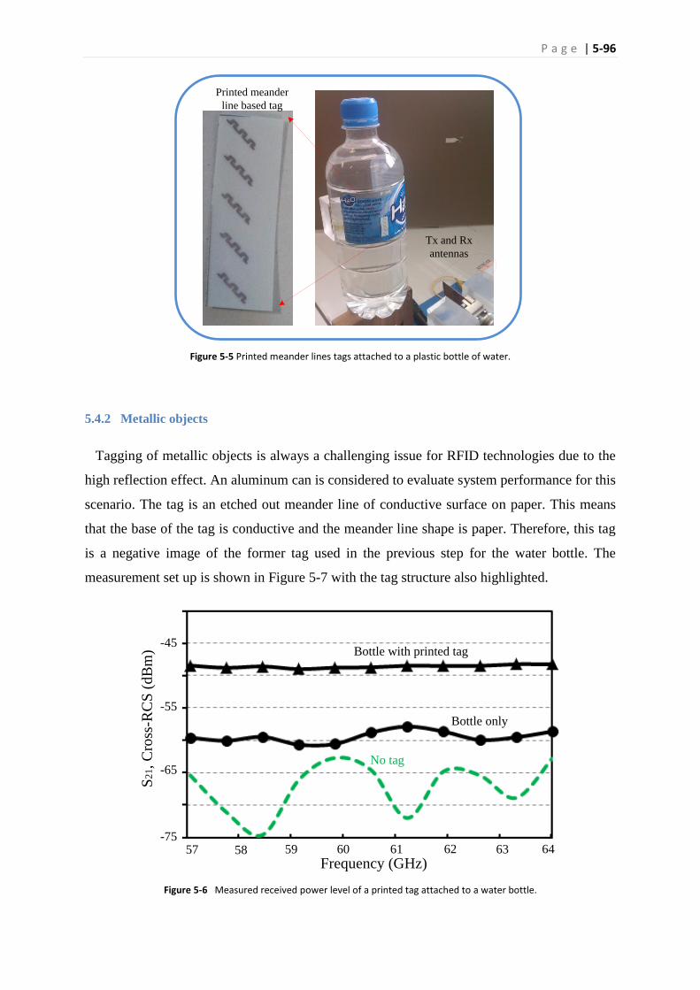
P a g e | 5-96
Figure 5-5 Printed meander lines tags attached to a plastic bottle of water.
5.4.2 Metallic objects
Tagging of metallic objects is always a challenging issue for RFID technologies due to the
high reflection effect. An aluminum can is considered to evaluate system performance for this
scenario. The tag is an etched out meander line of conductive surface on paper. This means
that the base of the tag is conductive and the meander line shape is paper. Therefore, this tag
is a negative image of the former tag used in the previous step for the water bottle. The
measurement set up is shown in Figure 5-7 with the tag structure also highlighted.
Figure 5-6 Measured received power level of a printed tag attached to a water bottle.
Tx and Rx
antennas
Printed meander
line based tag
Frequency (GHz)
S21, C
ross
-RC
S (
dB
m)
57 58 59 60 61 62 63 64
Bottle with printed tag
No tag
Bottle only
-75
-65
-55
-45

P a g e | 5-97
Figure 5-7 An etched out printed meander lines tag attached to an aluminium can.
Figure 5-8 Measured received power level of single layer printed tag attached to a water bottle.
Tx and Rx
antennas
Printed etched out
meander line based tag
Frequency (GHz)
S2
1, cr
oss
-RC
S (
dB
m)
57 58 59 60 61 62 63 64-75
-65
-55
-45
No tag
Can with printed tag
Can with no tag
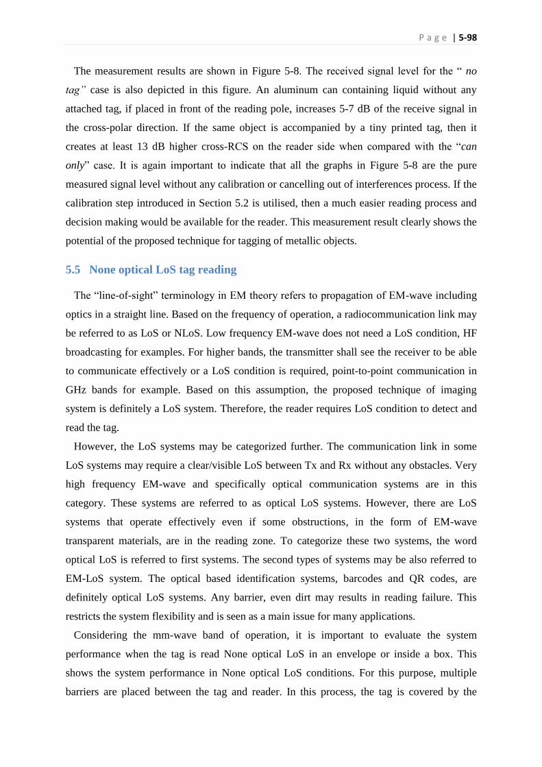
P a g e | 5-98
The measurement results are shown in Figure 5-8. The received signal level for the “ no
tag” case is also depicted in this figure. An aluminum can containing liquid without any
attached tag, if placed in front of the reading pole, increases 5-7 dB of the receive signal in
the cross-polar direction. If the same object is accompanied by a tiny printed tag, then it
creates at least 13 dB higher cross-RCS on the reader side when compared with the “can
only” case. It is again important to indicate that all the graphs in Figure 5-8 are the pure
measured signal level without any calibration or cancelling out of interferences process. If the
calibration step introduced in Section 5.2 is utilised, then a much easier reading process and
decision making would be available for the reader. This measurement result clearly shows the
potential of the proposed technique for tagging of metallic objects.
5.5 None optical LoS tag reading
The “line-of-sight” terminology in EM theory refers to propagation of EM-wave including
optics in a straight line. Based on the frequency of operation, a radiocommunication link may
be referred to as LoS or NLoS. Low frequency EM-wave does not need a LoS condition, HF
broadcasting for examples. For higher bands, the transmitter shall see the receiver to be able
to communicate effectively or a LoS condition is required, point-to-point communication in
GHz bands for example. Based on this assumption, the proposed technique of imaging
system is definitely a LoS system. Therefore, the reader requires LoS condition to detect and
read the tag.
However, the LoS systems may be categorized further. The communication link in some
LoS systems may require a clear/visible LoS between Tx and Rx without any obstacles. Very
high frequency EM-wave and specifically optical communication systems are in this
category. These systems are referred to as optical LoS systems. However, there are LoS
systems that operate effectively even if some obstructions, in the form of EM-wave
transparent materials, are in the reading zone. To categorize these two systems, the word
optical LoS is referred to first systems. The second types of systems may be also referred to
EM-LoS system. The optical based identification systems, barcodes and QR codes, are
definitely optical LoS systems. Any barrier, even dirt may results in reading failure. This
restricts the system flexibility and is seen as a main issue for many applications.
Considering the mm-wave band of operation, it is important to evaluate the system
performance when the tag is read None optical LoS in an envelope or inside a box. This
shows the system performance in None optical LoS conditions. For this purpose, multiple
barriers are placed between the tag and reader. In this process, the tag is covered by the
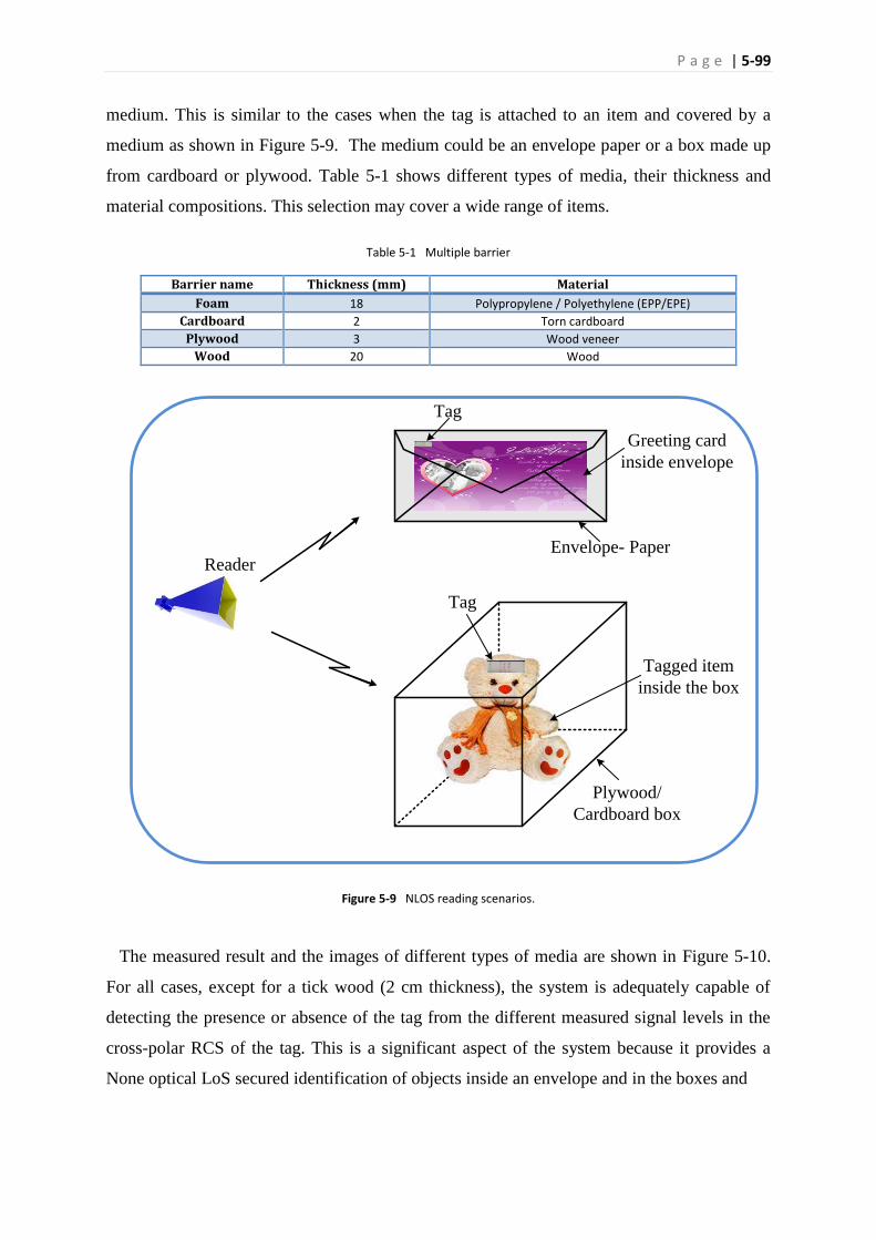
P a g e | 5-99
medium. This is similar to the cases when the tag is attached to an item and covered by a
medium as shown in Figure 5-9. The medium could be an envelope paper or a box made up
from cardboard or plywood. Table 5-1 shows different types of media, their thickness and
material compositions. This selection may cover a wide range of items.
Table 5-1 Multiple barrier
Barrier name Thickness (mm) Material
Foam 18 Polypropylene / Polyethylene (EPP/EPE)
Cardboard 2 Torn cardboard
Plywood 3 Wood veneer
Wood 20 Wood
Figure 5-9 NLOS reading scenarios.
The measured result and the images of different types of media are shown in Figure 5-10.
For all cases, except for a tick wood (2 cm thickness), the system is adequately capable of
detecting the presence or absence of the tag from the different measured signal levels in the
cross-polar RCS of the tag. This is a significant aspect of the system because it provides a
None optical LoS secured identification of objects inside an envelope and in the boxes and
Envelope- Paper
Greeting card
inside envelope
Tag
Plywood/
Cardboard box
Tagged item
inside the box
Tag
Reader
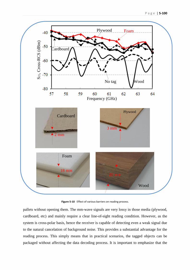
P a g e | 5-100
Figure 5-10 Effect of various barriers on reading process.
pallets without opening them. The mm-wave signals are very lossy in those media (plywood,
cardboard, etc) and mainly require a clear line-of-sight reading condition. However, as the
system is cross-polar basis, hence the receiver is capable of detecting even a weak signal due
to the natural cancelation of background noise. This provides a substantial advantage for the
reading process. This simply means that in practical scenarios, the tagged objects can be
packaged without affecting the data decoding process. It is important to emphasize that the
Frequency (GHz)
S2
1, C
ross
-RC
S (
dB
m)
WoodNo tag
FoamPlywood
Cardboard
20 mm
Wood
3 mm
Plywood
2 mm
Cardboard
18 mm
Foam

P a g e | 5-101
results in Figure 5-10 are without any calibration process. Obviously, if the environmental
effects are cancelled out with a predefined calibration process, then much cleaner signal level
differences between the two cases is observed. This process may ease reading of the tag
through 2 cm thick wood as well.
5.6 Bending effect on tag performance
In real identification and tracking applications, the attached tags, whether barcodes or RFID
types, are vulnerable to bending circumstances. This means that when the tag is attached to
an item for identification purposes, based on the shape of the item, the tag may not
necessarily be in a flat configuration. This issue affects the performance of the tag in its
decoding process. As the tag size increases, bending starts to be a serious issue as the
attached tag on a wider range of items experiences the bending effect. There are very limited
published works on the degradation of tag performance due to the bending of RFID tags or
even barcodes [118]. The proposed tag structure in the current research is physically
miniaturised one because of its mm-wave frequency band. Consequently the expectation is
that bending would not be a serious issue for a wide range of products to which the proposed
tag can be attached. Therefore, the system provides a fairly high robustness towards bending
due to its miniaturised nature. However, it is important to explore how tag bending may
affect the reading process, in a real scenario if the items are very small compared to the tag
size.
It is important to clarify the idea of bending on the proposed tag performance. The final tag
structure as is disclosed in Chapter 7 is a narrow strip with its width fixed at 1-1.5 cm and tag
length varying from 5-10 cm depending on the demanded data capacity. Consequently,
bending is expected to occur along the tag length and not on its width. Therefore, bending
affects the total tag structure and not any individual printed polariser. This idea is figuratively
shown in Figure 5-11.
As mentioned before, due to the very small size of the proposed tag structure, the attached
tag may not experience the bending degradation effect for a wide variety of products and
items. However for smaller items, the bending would be an issue in the overall system
performance. To verify the performance of the proposed meander line polariser-based tag
with respect to bending, small paper rolls of varying radii are prepared to which a tag can be
attached. These paper tubes are denoted as S-i; i = 1, 2, 3, 4. Figure 5-12 shows the tubes
along with their radius. For comparison purposes, a pencil is also included in Figure 5-12. To
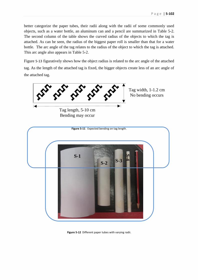
P a g e | 5-102
better categorize the paper tubes, their radii along with the radii of some commonly used
objects, such as a water bottle, an aluminum can and a pencil are summarized in Table 5-2.
The second column of the table shows the curved radius of the objects to which the tag is
attached. As can be seen, the radius of the biggest paper roll is smaller than that for a water
bottle. The arc angle of the tag relates to the radius of the object to which the tag is attached.
This arc angle also appears in Table 5-2.
Figure 5-13 figuratively shows how the object radius is related to the arc angle of the attached
tag. As the length of the attached tag is fixed, the bigger objects create less of an arc angle of
the attached tag.
Figure 5-11 Expected bending on tag length.
Figure 5-12 Different paper tubes with varying radii.
Tag length, 5-10 cm
Bending may occur
Tag width, 1-1.2 cm
No bending occurs
S-1
S-2S-3
S-4

P a g e | 5-103
Figure 5-13 Relation between arc angle of attached tag and radius of objects.
Table 5-2 Dimensions of paper tubes and some well-known items.
Attached items Curved radius,
R (cm)
Arc angle (°)
Paper tubes S-1 2.5 34°
Paper tubes S-2 1.25 68°
Paper tubes S-3 0.85 101°
Paper tubes S-4 0.35 245°
Aluminium can 3.25 26°
Water bottle 2.75 31°
Pencil 0.4 214°
Figure 5-14 shows the measurement set up for the bending effect of the tag. Again two
separate antennas are utilised as Tx and Rx which are located at 10 cm distance to the reading
pole. Antennas are connected to the VNA and the transmit power of the VNA at 60 GHz is
-5 dBm. The measured cross-polar components of the backscattered signal from various
curvatures are depicted in Figure 5-15. For objects bigger than S-1(R = 2.5 cm), bending has
a negligible effect on the received power level from the printed tag. Examples include a water
bottle and aluminum can. This clearly confirms system robustness for a wide variety of
objects. In other words, any object bigger than a water bottle experiences no bending effect
on the proposed technique. For objects on which their radii are R< 2.5 cm, the received
power level gradually decreases. However, the receiver still would be able to separate the
signal of a bent tag from a “no tag” case. Only for items smaller than S-4 (0.35 cm radius),
like a pencil, bending significantly degrades the system performance. For those items, the
received signal level is only 5 dBm higher than that of “no tag” case, which may create
Attached
tagR
Arc angle
Cross section of the
curved structure
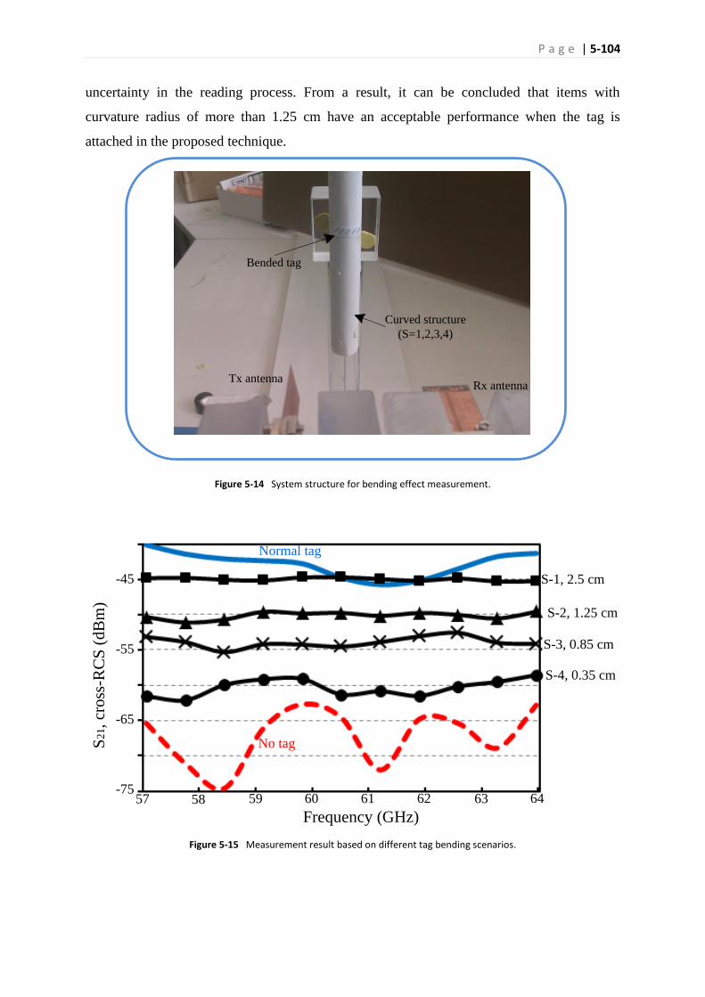
P a g e | 5-104
uncertainty in the reading process. From a result, it can be concluded that items with
curvature radius of more than 1.25 cm have an acceptable performance when the tag is
attached in the proposed technique.
Figure 5-14 System structure for bending effect measurement.
Figure 5-15 Measurement result based on different tag bending scenarios.
Tx antennaRx antenna
Curved structure
(S=1,2,3,4)
Bended tag
Frequency (GHz)
S21, cr
oss
-RC
S (
dB
m)
57 58 59 60 61 62 63 64-75
-65
-55
-45
No tag
Normal tag
S-1, 2.5 cm
S-2, 1.25 cm
S-3, 0.85 cm
S-4, 0.35 cm

P a g e | 5-105
5.7 Conclusion
In this chapter, printed meander line polarisers were considered in more detail. As the tag is
cross-polarised based, the performance of the meander line polarisers directly alleviate the
whole system capacity and performance.
First an analytical model of the reading scenario was developed based on radar theory. In
the proposed equivalent network of the system, the effects of Tx and Rx antennas, as well as
the connecting cables and connectors were considered. Then the tag was considered in the
communication channel between Tx and Rx antennas. Multipath and reflection from objects
around the tag were also reflected in the analytical model. The system was analysed
mathematically and it was shown that the system is very robust to multipath interferences.
Moreover, it was shown that co-polar based systems are very vulnerable to changes in the
reading zone and they require frequent system calibration. In contrast, the proposed cross-
polar system only involves one single calibration process and the tag movement or other
changes in the reading environment do not affect system performance. This issue was
nominated as a significant advantage of the proposed technique compared to other current
approaches in RFID applications, which are normally co-polar based.
Different measurement scenarios were considered for confirmation of the analytical model
of the system. First, a printed meander line-based tag was attached to a bottle of water. Then
an etched out printed meander line-based tag was considered as the negative image of the
normal printed meander lines for attaching to an aluminum can. In both cases, the tag reading
process was successfully accomplished. While the effects of the water bottle and aluminum
can without any attached tag were almost negligible in cross-polar direction, the presence or
absence of an attached printed tag could be easily detected by the reader system in a real
scenario. This step confirmed a noticeable potential of the proposed theory with respect to
other techniques in the RFID applications. Most proposed approaches in a chipless RFID
system normally face difficulty in reading the tag in the presence of highly reflective items.
Next, the system was tested for NLOS conditions. Different types of barriers were placed
between the tag and reader and then the system performance was measured. It was shown that
the reader easily detects the presence or absence of printed polarisers for a wide range of
barriers including, plywood, cardboard and paper. This suggests huge potential for the

P a g e | 5-106
proposed system on reading the tagged objects with an envelope or inside the box without the
requirement for opening them.
In the last part of this chapter, the effect of tag bending was considered. While tag bending
restricts the performance of the most chipless RFID systems, and there are not many
published works in this area, the proposed tag structure showed a very good performance for
a bent tag. This was initiated by the mm-wave band of operation, which resulted in
miniaturised tag size with very low bending vulnerability. Only for objects that are very small
and narrow, a pencil for example, the bending may affect the reading process in the proposed
chipless system.
The very successful performance of the proposed meander line as an effective EM-polariser
in harsh environments suggests a very robust system. Considering that all the measurements
were accomplished in a real laboratory environment using a poorly printed tag, it appears that
the proposed system for chipless RFID systems is fully practical for industrial applications.


P a g e | 6-107
Chapter 6 Reader antenna
6.1 Introduction
The working basis of the proposed cross-polar image-based chipless RFID system has
already been discussed in the last three chapters. Chapter 3 has shown that the linearly
polarised interrogation signal is converted to an orthogonally polarised wave through EM-
polarisers on the tag surface. The backscattered signal is picked up by the linearly polarised
receive antenna that is orthogonally oriented in respect to the transmit antenna. It was also
discussed in Chapter 3 that the proposed data encoding through EM-image of the tag requires
a very fine scanning of the tag surface which is technically possible only at mm-wave band of
60 GHz and higher frequencies. There are some more technical and operational requirements
for the reader that suggest a special antenna unit for the reader system. This chapter
introduces a suitable in-house antenna development for the reader for the proposed technique
of the cross-polar image-based system.
This chapter is organised as follow: it first reviews the technical and operational necessities
of the reader antennas for the proposed technique. This part builds the basis of further
activities in the rest of the chapter. Then the available or proposed antennas at the 60 GHz
band are reviewed to confirm that “off-the-shelf” products are not suitable for the demanded
requirements in the proposed approach.
When the actual demand for designing a new antenna set at 60 GHz is established, the
process of antenna design is introduced. Material characterisation at the intended frequency
band of 60 GHz, the proposed array of printed dipoles, the incorporated feeding network and
finally the measurement results of the antenna characteristics are discussed respectively in
detail. The developed antennas are used to read the proposed tag as introduced in the previous
chapters.
6.2 Technical and operational requirements of the antenna
In this section, it is intended to derive all the technical and operational requirements of the
reader antenna in the proposed technique. Based on these necessities, the antenna type and its
characterisations are later constructed.

P a g e | 6-108
As the system is based on the separation of transmit and receive signals through an
orthogonal polarisation scheme, the ability of the antenna to distinguish two polarisations is
very important. This characteristic of the antenna is known as its cross-polar level (CPL). The
CPL defines the quality of the signal polarisation. In other words, the ratio of the desired
polarisation to the orthogonal/cross-component is known as the antenna CPL:
1 ; ( ) 20 log( )Desired field component
CPL CPL CPL dB CPLCross polar field component
(6.1)
In the proposed system, both transmit and receive antennas are close to each other and the
transmit module doesn’t require any switching mechanism. Therefore the high CPL, in order
of 15-20 dB, is essential for the antennas. Otherwise, the direct signal leakage from
transmitter to receiver due to the low isolation of the antennas may saturate the receiver and
affect the tag reading process. The higher the CPL, the better is the receiver sensitivity with
respect to the cross-polar tag response.
As was already shown in Chapter 3, a fine EM-image resolution on the tag surface is only
accomplished through an advanced imaging technique, like SAR. In the SAR-based system,
the reader moves around the tag to create a synthetic aperture. The received signals by the
antennas at the designated positions are collected for further processing. This mandates a
wide azimuth radiation pattern of the antenna to make it possible for illumination of the tag
surface from different view angles. As is discussed in the next chapter, the length of the
synthetic aperture depends on the tag size and the reading distance, however, the aperture size
normally varies between 15-25 cm for a 10 cm reading distance.
Figure 6-1 shows the reading distance and the required half power beamwidth (HPBW) of
the antenna in the azimuth direction. To consider the worst case, the synthetic aperture of 30
cm is considered in Figure 6-1 while the reading distance is 10 cm. The angle θ is therefore:
1 10
tan 3315
(6.2)
And from (6.2), the HPBW would be:
2 (90 ) 114HPBW (6.3)
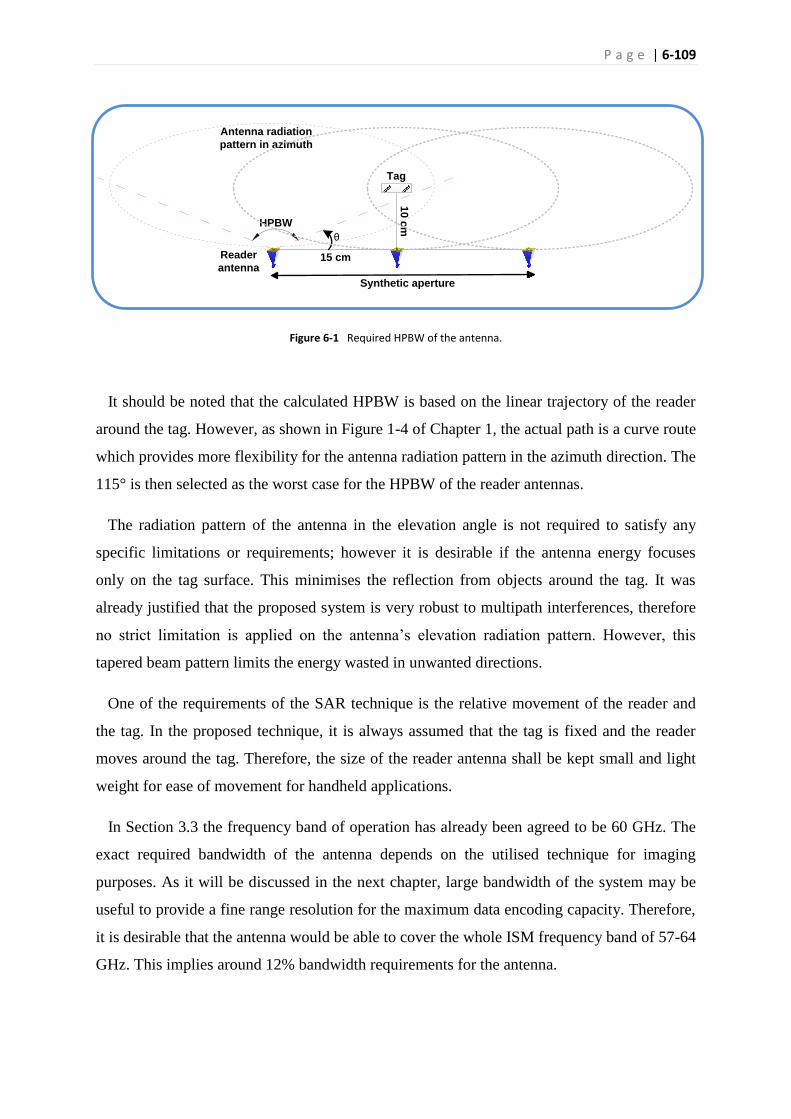
P a g e | 6-109
Figure 6-1 Required HPBW of the antenna.
It should be noted that the calculated HPBW is based on the linear trajectory of the reader
around the tag. However, as shown in Figure 1-4 of Chapter 1, the actual path is a curve route
which provides more flexibility for the antenna radiation pattern in the azimuth direction. The
115° is then selected as the worst case for the HPBW of the reader antennas.
The radiation pattern of the antenna in the elevation angle is not required to satisfy any
specific limitations or requirements; however it is desirable if the antenna energy focuses
only on the tag surface. This minimises the reflection from objects around the tag. It was
already justified that the proposed system is very robust to multipath interferences, therefore
no strict limitation is applied on the antenna’s elevation radiation pattern. However, this
tapered beam pattern limits the energy wasted in unwanted directions.
One of the requirements of the SAR technique is the relative movement of the reader and
the tag. In the proposed technique, it is always assumed that the tag is fixed and the reader
moves around the tag. Therefore, the size of the reader antenna shall be kept small and light
weight for ease of movement for handheld applications.
In Section 3.3 the frequency band of operation has already been agreed to be 60 GHz. The
exact required bandwidth of the antenna depends on the utilised technique for imaging
purposes. As it will be discussed in the next chapter, large bandwidth of the system may be
useful to provide a fine range resolution for the maximum data encoding capacity. Therefore,
it is desirable that the antenna would be able to cover the whole ISM frequency band of 57-64
GHz. This implies around 12% bandwidth requirements for the antenna.
10
cm
15 cm
Antenna radiation
pattern in azimuth
HPBW
θ
Tag
Reader
antenna
Synthetic aperture
P a g e | 6-110
In conclusion, it appears that the followings are the intended requirements of the reader
antenna(s) for the proposed cross-polar image-based chipless RFID system:
(i) Operating at frequency band 57-64 GHz.
(ii) High cross-polar level in boresight direction, CPL > 15dB.
(iii) Fan-shaped radiation pattern with wide azimuth beamwidth >115° azimuth and
desirable elevation beamwidth <15°.
(iv) Light weight and small size for handheld applications of the reader.
In the following section, a review of the reported 60 GHz antennas is presented followed by
the proposed double side printed dipole array (DSPD) antenna at 60 GHz.
6.3 Off-the-shelf products
It was discussed that the 60 GHz band has already been used for inter-satellite
communication links or for highly secure terrestrial mobile communication. The recent
release of 57-64 GHz as an ISM band accelerates many products on this band for public
usage [32, 94, 113, 119].
However, the higher attenuation of signals related to the 60 GHz band suggests a high gain
antenna for short range communications links, in the order of few kilometres. Few available
antennas have been found on the market which work on the intended frequency band,
however their radiation pattern and impedance bandwidth appear to be unsuitable for the
purposed chipless RFID system. Nokia’s radio link Metro Hopper [120] is a high data rate
communication link but only covers 57.2-58.2 GHz and has a large antenna size that is not
suitable for the proposed chipless RFID application. Proxim [121] suggests products at 60
GHz which utilise antennas for covering the whole band of 57-64 GHz. The gains of antennas
range from 25-35 dBi. There is no information about the radiation pattern but high antenna
gain suggests a large aperture size and narrow radiation pattern, which do not satisfy the
required specifications for the image-based chipless RFID application. Moreover, no
information about the polarisation cross-polar level is disclosed. Normally the ISM band of
57-64 GHz has been taken by companies for providing high data rate communication in
point-to-point links [92, 93].
P a g e | 6-111
Therefore, it is expected that the proposed antennas in those applications have high gain
and a narrow radiation patterns. Moreover, the antenna size is not an issue in those
applications. Therefore, it is unlikely to be able to find an off-the-shelf antenna, which
satisfies the necessities of the reader antenna for the proposed chipless RFID application.
6.4 Proposed array of printed dipoles
The general specifications of the required antenna outlined in Section 6.2 govern the type of
suitable solution for the proposed reader antenna. One may suggest that an array of printed
dipole antenna is a suitable candidate to meet the specification requirements. The printed
antenna adequately satisfies the requirements of low profile, light weight and low cost
attributes of the chipless RFID system. Dipole antennas provide wide radiation patterns in the
azimuth direction, while their HPBW in the elevation angle depends on the dipole length.
Moreover, the array configuration also provides the opportunity for controlling the
beamwidth in the desired direction. Dipoles are normally linearly polarised antennas and are
able to provide adequate cross-polar level for many applications. The compact size of the
dipoles is another positive aspect for the proposed system. A printed dipole enjoys a few
advantages over a microstrip patch antenna. They provide wider bandwidth, lower loss and
less parasitic radiation of feed lines [122-125]. The candidate antenna is a double side printed
dipole (DSPD). When compared with a single side printed dipole, the DSPD yields broader
bandwidth and higher gain [126, 127].
Nesic [122] reports a one-dimensional array of printed dipoles fed by a microstrip line at 5
GHz with 7% bandwidth. The antenna works on its third resonance so provides higher gain
than that of its first resonance. However, the very low antenna bandwidth on its third
resonance has been mitigated by penetrating the feed line between two slots. No information
on the radiation pattern of the antenna was disclosed in the report. Scott [127] shows a
microstrip-fed printed dipole array using a microstrip-to-coplanar stripline (CPS) balun. In
[122] and [127], the balun were not easy to match the impedance, and the structures were too
big and bulky, hence, it was complicated to build an array structure [128].
Brankovic patented a pentagonal dipole antenna on a 64-element array configuration
yielding 25% bandwidth at 60 GHz [129]. The radiation pattern of this work is not wide in
the azimuth direction, and also no information of the cross-polar level was declared.
Considering the pentagonal radiator shape, the lower cross-polar level is expected than that of

P a g e | 6-112
a normal dipole. Suh and Chang [128] report a 30 GHz printed dipole that has microstrip-fed
coplanar stripline Tee junctions and yields 3% bandwidth. Alhalabi [130] showed a high-
efficiency array of printed dipoles designed at 22-26 GHz. Varying feed line lengths create
prescribed phase shifts between array elements. The same author also proposed a 60 GHz
single dipole antenna [131] suitable for laptops and portable communication devices. From
the above reviews it can be concluded that none of the reported antennas at 60 GHz are
suitable for the proposed RFID system, However, the approaches proposed in [130] is
generally followed to build a suitable reader antenna for the proposed application. As
discussed before, the reader antenna for the proposed application requires satisfying a set of
specifications that are necessary for different reasons. An array of DSPD fulfils all of the
requirements outlined previously and repeated in Table 6-1.
Table 6-1 Technical and operational requirements of the reader antenna
Centre Frequency 60.5 GHz
Bandwidth 12%
Radiation pattern Maximum 15° on E-plane
Minimum 115° on H-plane
Cross-polar level >15 dB
Substrate
Low thickness for high cross-polar level
Stable electrical and mechanical
performances on mm-wave region
Gain Between 5-10 dBi
Dimension As small as possible(centimetre order)
In the design process, the first step is to select an appropriate substrate for the printed dipole
antennas. The suggested dielectric is the Taconic TLX-8 since the authors group has an
extensive experience with its performance at 24-27 GHz [132]. However, as the constitutive
parameters, such as dielectric constant εr and loss tangents tanδ of Taconic substrate TLX-8,
are not known at 60 GHz, a special test jig is built to measure the substrate parameters at 60
GHz. The next step is to design the dipole as the array radiating element. The dipoles are
equipped with an unbalanced feed line which then is converted to a microstrip line. A
microstrip to coplanar waveguide (CPW) feedline transition facilitates a V-type input
connector assembly to be added with the array antenna. The array structure is precisely
optimised to cover the entire band of 57-64 GHz yielding 12% bandwidth at 60 GHz. The
flowchart of the DSPD array antenna design that yields a wide bandwidth and high cross-
polar level for the image-based chipless RFID reader is shown in Figure 6-2. Each section of
the design process outlined in Figure 6-2 is presented separately, and then the fabricated array
is tested proving its actual potential for the proposed application.

P a g e | 6-113
Figure 6-2 Design flowchart for array of DSPD’s.
6.5 Substrate selection and characterisation
6.5.1 Substrate selection and thickness
The first step of antenna design is the selection of the substrate. The frequency of operation
and required bandwidth govern the selection of the substrate. Substrate thickness, relative
permittivity, loss tangent, copper thickness, and finally mechanical and thermal stabilities are
the important factors of the substrate at 60 GHz. Precision in the design and substrate
properties are critical for design success considering the 5 mm wavelength of the 60 GHz
band.
As introduced previously, Taconic TLX-8 would be a suitable candidate as it satisfies many
of the aforementioned factors [133, 134]. Its low dielectric constant enhances the antenna
efficiency and bandwidth and its thin thickness is favourable for the high cross-polar level
[18]. The substrate thickness is the first parameter to be selected. It is normally bonded by
two contradictory factors. A thin substrate is required to minimize surface wave and hence
for an efficient radiator while large required operational bandwidth of 12% suggests a thick
substrate [135]. The substrate thickness should satisfy (6.4) to ensure the suppression of
higher order radiation modes on the dielectric surface [136]. Based on (6.4), the substrate
thickness must be less than 1 mm at 60 GHz.
Thickness 0
- 14r eff
1.06 mm (6.4)
Start
SUBSTRATE
· Type and thickness
· Characterisation
DSPD design
· Dipole design
· Chamfering
· GND tapering
· Radiation and CPL
ARRAY DESIGN
· Beam forming
· Feeding network
· Mutual coupling
· Feed line extension
MEASUREMENT
· Reflection coefficient
· Radiation pattern
· Gain
· Imaging application
Conclusion
END

P a g e | 6-114
In (6.4), the wavelength(λ0) is between 4.68-5.26 mm for 57-64 GHz. εreff is the effective
permittivity of the substrate. Considering the available commercial Taconic products, the
Taconic TLX-8 with 0.127 mm thickness is selected. This thickness adequately satisfies (6.4)
and ensures that only one surface wave, TM0 with zero cut-off frequency exists in the
substrate [137]. This thin substrate also enhances the cross-polar level of the antenna which is
a critical aspect of the design [138].
6.5.2 Substrate characterisation
The knowledge of the actual constitutive parameters of the substrate is vital for accurate
design, especially in the mm-band where dimensions based on the substrate characteristics,
such as the relative permittivity and loss tangent, are tolerance-critical. Today, most substrate
manufacturers specify the dielectric parameters of their materials at 10 GHz. Consequently,
in the realised design at mm-band, frequency shifts attributed to permittivity deviation
commonly occur [139]. Microwave measurement techniques to determine substrate
permittivity and loss tangent at specific frequencies are [140, 141]: (i) transmission and
reflection, and (ii) resonance techniques. Transmission and reflection techniques can be used
to obtain the real part of the relative permittivity for a high or low loss specimen, but lack the
resolution to measure low loss tangents. Resonant techniques are only suitable for low loss
materials since the resonance curve broadens as the loss increases [142]. Usually, dielectric
measurement using a resonance technique provides higher accuracy than that obtained from a
transmission and reflection technique. It is, therefore, considered the most accurate method
for dielectric constant and loss tangent measurement of planar structures. Considering the
structural dimensions at the mm-band, the substrate integrated waveguide (SIW) resonators
approach is proposed for substrate characterisation at the V and W-bands [140].
A Taconic [133] published data sheet of the TLX-8 at 10 GHz reveals the following
information: r = 2.55 and tan = 0.0019. To measure the actual electrical parameters of the
substrate at 60 GHz, the SIW cavity resonators are designed and fabricated at this band.
Propagation and attenuation constants of a SIW resonator are related to the modal expansion
theory of a rectangle waveguide [141]. Expression (6.5) shows the equivalent dimensions of
the rectangle waveguide on which a, b, d, and s are defined in Figure 6-3. The number of via
holes are 10 and 11 for a and b directions respectively as shown in the photograph of the
sample SIW in Figure 6-4. The resonance frequency of the rectangle SIW resonator for TEmn0

P a g e | 6-115
mode relates to the resonance frequency of the rectangle waveguide and can be calculated by
(6.5) [143]:
0
2 2
2mn
eff effr
c m nf
a b
(6.5)
where aeff and beff can be derived from (6.6), c is the light speed in free space, and εr is
the effective dielectric constant.
2 2
1.08 0.1 ; ,eff
d dx x x a b
s x (6.6)
Figure 6-3 Layout of sample SIW resonator with via holes [24].
Figure 6-4 Photograph of SIW resonator for dielectric constant and loss tangent measurement of Taconic TLX-8 [140].
b
a
GND
y
sd
Feeding point
h
Dielectric
SIW resonator

P a g e | 6-116
To find the effective dielectric constant, the proposed approach by Zelenchuk et al. [140] is
followed. Six prototypes of SIW resonators are fabricated and tested to measure the substrate
parameters at 60 GHz. The average dielectric constant of all six samples suggests the
effective dielectric constant of the substrate, Taconic TLX-8, at 60 GHz. This average value
for the six samples of SIW resonators is εr = 2.25. The average measured loss tangent is
0.0072 but there is a sample with a higher loss tangent. Therefore, the worst case is
considered that is 0.01. These two values of the constitutive parametres of the substrate are
substantially different from those for the published datasheet at 10 GHz. Table 6-2
summarises the results of the dielectric parameters at different frequencies. The new values of
the substrate parameters of the substrate at 60 GHz are considered in the design process of the
proposed DSPD array antenna.
Table 6-2 Dielectric parameters of Taconic TLX-8
60 GHz r = 2.25 tan = 0.01
10 GHz r = 2.55 tan = 0.0019
The measurement was performed with error correction calibration using an Agilent
performance network analyser (PNA) E8361A. The accurate characterisation ensures the full
wave EM solver CST Microwave Studio simulation results match with the measured data of
the prototype array antenna.
6.6 Double side printed dipole
As discussed in Section 6.4, the proposed antenna is an array of double sided printed
dipoles (DSPD). Hence, the first step of the design process is to design the appropriate array
radiator element. The DSPD element with the design parameters is shown in Figure 6-5. The
length of the dipole arm (La) mainly controls the resonance frequency of the dipole. It is also
a function of the substrate thickness, h, and dielectric constant, εr. As the substrate does not
cover the whole structure, the resonant length is not scaled with 1/√εreff as does an antenna in
a homogeneous medium [20]. The initial value of the dipole length is related to the frequency
of operation, f, and to the medium by (6.7) and (6.8) [26]:
(2 ) 0.47 ;a
reff
vDipole length L
f
cv
(6.7)

P a g e | 6-117
2
1 1 121 0.04
2 21ff
ar r
are
h
w
w
h
(6.8)
In (6.7) and (6.8), v is the velocity of EM wave propagation inside the substrate, c is the
speed of light in the free space and the rest of the parameters are defined in Figure 6-5. Based
on (6.7) and (6.8), the required length of the dipole arm is 1.2 mm. This initial length is
entered in full-wave EM solver CST Microwave Studio and the design is optimised to meet
the specification requirements. After parameter sweeping in the CST, the simulated dipole
arm length is 1 mm. The shorter length of the dipole through full wave simulation is due to
the fact that the physical length of the dipole is always bigger than its electrical length. Hence
the 1.2 mm dipole arm corresponds to the resonance at lower frequencies than that expected
through (6.7).
The width of the dipole arm (Wa) is independently optimised to provide 50 Ω input
impedance for the individual dipole. However, on the other hand, the parallel suspended feed
line of the dipole arm is transformed to a microstrip line above the ground plane. The
microstrip feedline is also expected to provide the 50 Ω input impedance for the
beamforming network of the array antenna.
The width of the microstrip line, Wf, is also designed independently. Two widths of Wa and
Wf obviously are different as they are different types of transmission lines. Matching of these
two transmission lines with different widths is manipulated by changing the chamfering depth,
Cd. To enhance the bandwidth and performance of the array radiator, chamfering of the
dipole element and tapered ground plane at the suspended parallel stripline to micro-strip line
transition are used.
Figure 6-5 Single dipole, Wf = 0.37, FL = 1.05, Fa = 0.55, Wa = 0.19, La = 1, Cd = 0.2 and h = 0.127, all in mm.
Fa
Cd
La
FL
Wf
h
GND
Wa
Subs
trat
e
P a g e | 6-118
These techniques yield more than 12% bandwidth at 60 GHz while conventional design
yields 7% bandwidth [20]. The following sections describe the matching techniques
envisaged to enhance the radiator performance.
6.6.1 Dipole chamfering
Dipole antennas are inherently unbalanced circuits and create distortion in radiation
patterns. Connecting a dipole to a feed line requires a balun network to match balanced and
unbalanced circuits [143, 144]. There are many different types of balun networks based on
the dipole antenna structure. Chen [145] suggests a double sided feed network on the
substrate as the balun network for the planar dipole antennas. The bottom-tapered ground
transition is designed to provide an impedance matching tuner with balanced output. The
designed feeding network of the dipole antenna with the tapered balun transition is tuned by
the angle of the tapered ground plane for impedance matching and balanced output. Almost
the same balun structure is followed for the proposed array antenna. As shown in Figure 6-5,
the double sided feed line provides a smooth transition between the unbalanced and balanced
currents of the line that is connected to the ground plane and the dipole feed respectively.
This configuration also simplifies the balun network. The proposed balun network does not
require the bottom-tapered transition as suggested by Chen [145]. It is discussed in the next
section why an abrupt bottom transition is selected instead of a tapered one.
As discussed earlier, chamfering of the dipole edge is required to match two different
widths of the feedline (wf) and dipole arm (wa). Moreover, the right angle of the microstrip
line creates an extra capacitance and also changes the electrical length of the line [146].
These two factors affect the impedance matching of the printed dipole structure and create
signal reflection from the dipole and the feedline. Chamfering of the dipole edge where the
dipole arm is connected to the feedline and the ground plane compensates those two effects.
For symmetry, both dipole arms at their right angle transitions are supposed to be chamfered.
However, from investigation in full-wave CST Microwave Studio simulation, it was found
that only top arm chamfering provides best results. Figure 6-6 shows the input impedance
return loss (S11 in dB) versus frequency for three cases: top arm, both arms and no
chamfering at all. Considering the effect of different chamfering scenarios on the input
impedance, the maximum RL of 27 dB is obtained with top arm chamfering. As the bottom
arm is directly connected to the ground via the bottom feedline structure, it has a minor effect
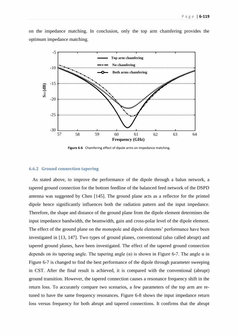
P a g e | 6-119
on the impedance matching. In conclusion, only the top arm chamfering provides the
optimum impedance matching.
Figure 6-6 Chamfering effect of dipole arms on impedance matching.
6.6.2 Ground connection tapering
As stated above, to improve the performance of the dipole through a balun network, a
tapered ground connection for the bottom feedline of the balanced feed network of the DSPD
antenna was suggested by Chen [145]. The ground plane acts as a reflector for the printed
dipole hence significantly influences both the radiation pattern and the input impedance.
Therefore, the shape and distance of the ground plane from the dipole element determines the
input impedance bandwidth, the beamwidth, gain and cross-polar level of the dipole element.
The effect of the ground plane on the monopole and dipole elements’ performance have been
investigated in [13, 147]. Two types of ground planes, conventional (also called abrupt) and
tapered ground planes, have been investigated. The effect of the tapered ground connection
depends on its tapering angle. The tapering angle (α) is shown in Figure 6-7. The angle α in
Figure 6-7 is changed to find the best performance of the dipole through parameter sweeping
in CST. After the final result is achieved, it is compared with the conventional (abrupt)
ground transition. However, the tapered connection causes a resonance frequency shift in the
return loss. To accurately compare two scenarios, a few parameters of the top arm are re-
tuned to have the same frequency resonances. Figure 6-8 shows the input impedance return
loss versus frequency for both abrupt and tapered connections. It confirms that the abrupt
Frequency (GHz)
57 58 59 60 61 62 63 64
-5
-10
-15
-20
-25
-30
Top arm chamfering
No chamfering
Both arms chamfering
S1
1 (d
B)

P a g e | 6-120
connection offers better impedance matching at the resonance frequency. This is what is
normally expected for an abrupt connection. In fact, the logical expectation is to have lower
bandwidth through abrupt connection than the tapered type ground connection. However, as
shown in Figure 6-8, the abrupt and tapered connections successfully cover the whole
frequency band of interest 57-64 GHz. Therefore, the abrupt type ground connection is
selected for the proposed DSPD array antenna structure. This effect was also experienced by
Alhalabi [13] over the lower frequency range of 20-26 GHz.
Figure 6-7 Embedded DSPD antenna with tapered ground connection.
Figure 6-8 Ground connection's effect on matching of dipole.
α
Top plane
Bottom plane
Tapered
ground
Abrupt
ground
S11 (
dB
)
57 58 59 60 61 62 63 64
0
-10
-20
-30
Frequency (GHz)
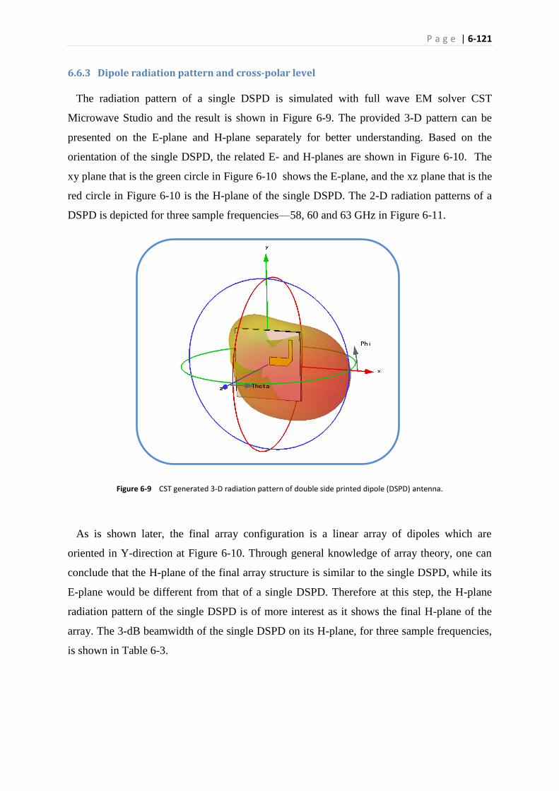
P a g e | 6-121
6.6.3 Dipole radiation pattern and cross-polar level
The radiation pattern of a single DSPD is simulated with full wave EM solver CST
Microwave Studio and the result is shown in Figure 6-9. The provided 3-D pattern can be
presented on the E-plane and H-plane separately for better understanding. Based on the
orientation of the single DSPD, the related E- and H-planes are shown in Figure 6-10. The
xy plane that is the green circle in Figure 6-10 shows the E-plane, and the xz plane that is the
red circle in Figure 6-10 is the H-plane of the single DSPD. The 2-D radiation patterns of a
DSPD is depicted for three sample frequencies—58, 60 and 63 GHz in Figure 6-11.
Figure 6-9 CST generated 3-D radiation pattern of double side printed dipole (DSPD) antenna.
As is shown later, the final array configuration is a linear array of dipoles which are
oriented in Y-direction at Figure 6-10. Through general knowledge of array theory, one can
conclude that the H-plane of the final array structure is similar to the single DSPD, while its
E-plane would be different from that of a single DSPD. Therefore at this step, the H-plane
radiation pattern of the single DSPD is of more interest as it shows the final H-plane of the
array. The 3-dB beamwidth of the single DSPD on its H-plane, for three sample frequencies,
is shown in Table 6-3.
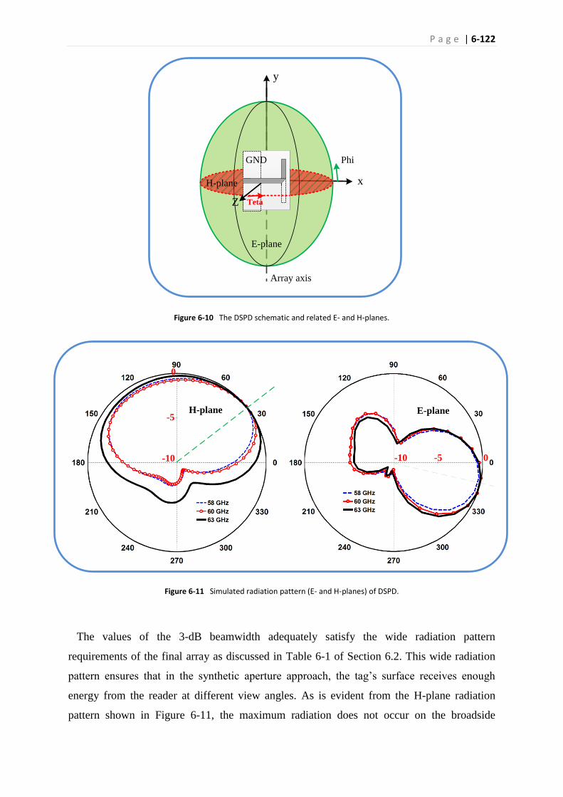
P a g e | 6-122
Figure 6-10 The DSPD schematic and related E- and H-planes.
Figure 6-11 Simulated radiation pattern (E- and H-planes) of DSPD.
The values of the 3-dB beamwidth adequately satisfy the wide radiation pattern
requirements of the final array as discussed in Table 6-1 of Section 6.2. This wide radiation
pattern ensures that in the synthetic aperture approach, the tag’s surface receives enough
energy from the reader at different view angles. As is evident from the H-plane radiation
pattern shown in Figure 6-11, the maximum radiation does not occur on the broadside
x
y
Z Teta
Phi
E-plane
H-plane
Array axis
GND
E-plane
0-5-10
H-plane
0
-5
-10
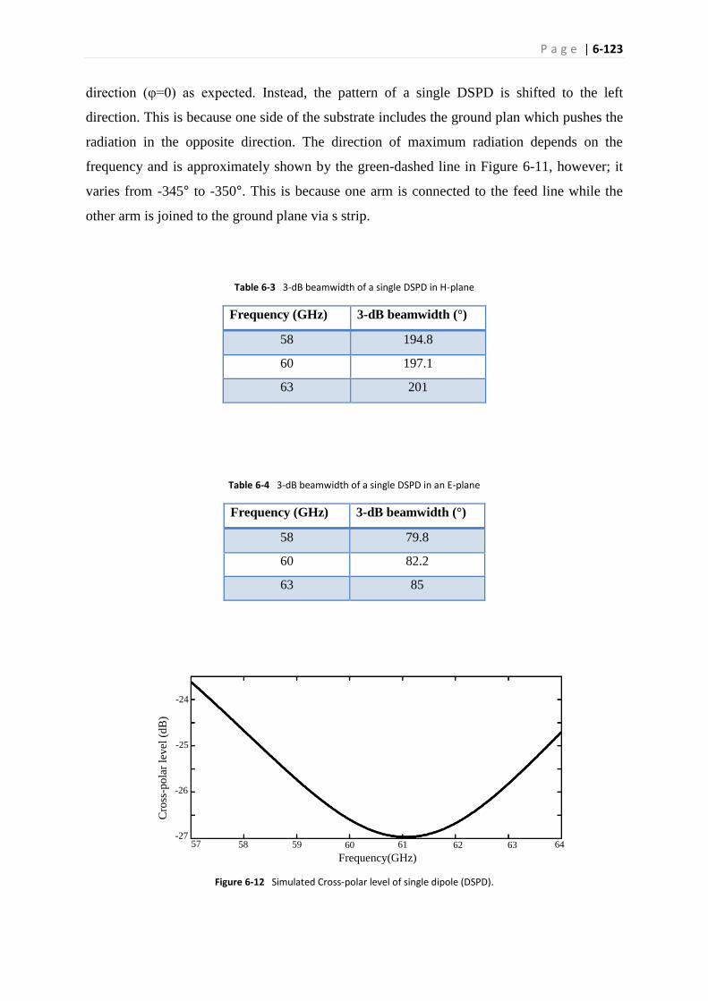
P a g e | 6-123
direction (φ=0) as expected. Instead, the pattern of a single DSPD is shifted to the left
direction. This is because one side of the substrate includes the ground plan which pushes the
radiation in the opposite direction. The direction of maximum radiation depends on the
frequency and is approximately shown by the green-dashed line in Figure 6-11, however; it
varies from -345° to -350°. This is because one arm is connected to the feed line while the
other arm is joined to the ground plane via s strip.
Table 6-3 3-dB beamwidth of a single DSPD in H-plane
Frequency (GHz) 3-dB beamwidth (°)
58 194.8
60 197.1
63 201
Table 6-4 3-dB beamwidth of a single DSPD in an E-plane
Frequency (GHz) 3-dB beamwidth (°)
58 79.8
60 82.2
63 85
Figure 6-12 Simulated Cross-polar level of single dipole (DSPD).
Frequency(GHz)
57 58 59 60 61 62 63 64
-24
-25
-26
-27
Cro
ss-p
ola
r le
vel
(d
B)

P a g e | 6-124
Although, the 3-dB beamwidth of the E-plane radiation pattern of the final structure would
be different from that of the single DSPD, for completion, the sample values of the 3-dB
beamwidth are shown in Table 6-4.
As discussed in Section 6.2, the quality of the antenna polarisation known as its cross-polar
level is a critical parameter in the proposed application. For the designed single DSPD, the
cross-polar level is simulated by having co- and cross-polar probes in CST Microwave studio
and measuring the S21 of the link. The simulated cross-polar level for a single DSPD is
depicted in Figure 6-12. Over the entire frequency range of operation, this ratio for a single
dipole is less than -23 dB. There is the opportunity of decreasing the cross-polar level by
simply using the defected ground structure (DGS) [29]. However the provided -23 dB cross-
polar level through the DSPD adequately satisfies the requirements of the proposed
application, as is shown in the next chapter where the final signal processing results are
revealed.
6.7 Array design
6.7.1 Required beamforming array
The antenna specifications discussed in Section 6.2 governs the array structure. From the
beamforming aspect, as a fan shaped radiation pattern, wide azimuth and narrow elevation is
required, then a linear array type would satisfy this specification. Multiple vertically aligned
dipoles narrow the radiation pattern in the elevation angle. For the suggested 15° beamwidth
in the elevation angle, see Table 6-1, an array of four elements would be satisfactory. The
wide H-plane radiation pattern of a single DSPD as shown in Figure 6-11 fulfils the 115°
required azimuth beamwidth. To select a proper feed network, the overall system structure
for the image-based chipless RFID application shall be considered. In the proposed
application, the antenna moves around the tag and illuminates the tag through different angles.
The relative position of the tag and antenna is considered in the SAR-based signal processing
to reveal the EM-image of the tag. Therefore, it is mandatory that the antenna has a unique
and fixed radiation pattern shape in all positions during capturing of the backscattered signals
from the tag. This is the reason why a phased array antenna wouldn’t be a suitable candidate
for this application as a phased array antenna creates various beam shapes on different angles
[148]. From array theory, it is clear that the uniform excitation of the array’s elements creates
the maximum radiation intensity and the minimum 3-dB beamwidth in the boresight direction

P a g e | 6-125
[144]. Therefore, the requirement for a fixed fan shaped radiation pattern with the minimum
beamwidth suggests a linear array of dipoles with uniform array excitation. A 4-elements
array of DSPD’s provides the required performance as calculated in Table 6-1.
6.7.2 Corporate feeding network
The requirement for a uniform excitation of the array elements and also having two separate
Tx and Rx antennas at the reader side ease the power divider arrangement. A T-junction
corporate feed power divider is one of the simplest type of power dividers and is used for the
proposed application [149]. It is fully printable and low cost without any lumped element in
the structure. These advantageous features make the T-junction power divider a very suitable
candidate for feeding the DSPDs on the array structure. However, the T-junction power
divider suffers from two major limitations. First, it utilises quarter wavelength transformer in
its structure that restricts the operation bandwidth of the element. Second, it provides low
isolation among output ports. The low isolation would be a major limitation for mono-static
systems on which the same antenna is used for transmit and receive purposes. While in the
proposed bi-static configuration, two separate antennas are utilised, therefore, the low
isolation of the output is not an issue. The low bandwidth of the power divider, due to the
quarter wavelength transformer, can be compensated by minor changes in the component
design. Figure 6-13 shows a conventional two-way T-junction power divider and its
dimensions. The length of the quarter wavelength transformer is fixed and it is intended to
transform 50 Ω impedance to the 100 Ω. The length of the 50 Ω arm on each side of the
Figure 6-13 T-junction power divider.
0.525 mm
λ/4 transformer
50Ω line 100Ω point
Power divider’s
variable arm
0.35 mm
0.2 mm
Cha
mfe
ring
dept
h

P a g e | 6-126
power divider depends on the required physical distance between two connected dipoles. The
chamfering depth is optimised through parameter sweep in the CST simulation tools.
The T-junction power divider, shown in Figure 6-13, normally acts properly in a narrow
band operation. However, to enhance the power divider bandwidth, it is normally suggested
to have a small V-notch in the dividing point of the T-junction structure, 100 Ω point in
Figure 6-13. This gap is shown in Figure 6-14(a). In the current work however, it was found
that a reactive stub acts better and can enhance the power divider bandwidth. The T-junction
power divider with a reactive stub is also shown in Figure 6-14(b). The dimensions of the
reactive stub are optimised through parameter sweeping of CST.
The corporate feed network of the proposed array antenna includes three two-way
T-junction power dividers. This complete feed network is shown in Figure 6-15. As one can
see, the length of the quarter wavelength transformer is the same for all three T-junctions.
The lengths of the power dividers’ arms vary based on the required physical distance between
the radiators in the array configuration. The S-parameter of the corporate feed network is
depicted in Figure 6-16. Figure 6-16 shows that S11 in dB versus frequency is adequately
below -15 dB over the whole frequency range of operation. The minimum value of the
reflection coefficient is -20.5 dB at 61.5 GHz. This is a noticeable result considering the
narrowband aspect of the quarter wavelength sections in the power divider structure.
Normally, four transmission coefficient curves are expected in Figure 6-16. However, as the
transmission coefficients of each port (SjI where j = 1, 2, 3, 4) are similar, only two of them
are depicted as an example.
Figure 6-14 T-Junction power divider with a) V-notch b) reactive stub.
a)
b)
V-notch
Reactive stub
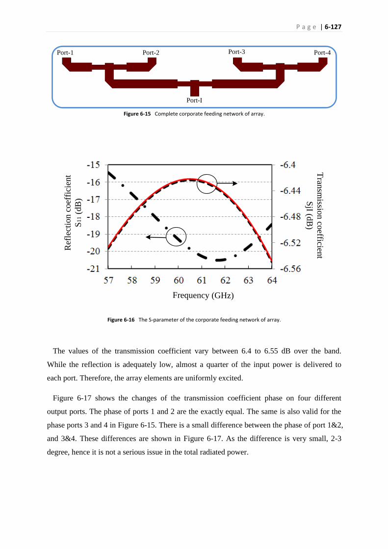
P a g e | 6-127
Figure 6-15 Complete corporate feeding network of array.
Figure 6-16 The S-parameter of the corporate feeding network of array.
The values of the transmission coefficient vary between 6.4 to 6.55 dB over the band.
While the reflection is adequately low, almost a quarter of the input power is delivered to
each port. Therefore, the array elements are uniformly excited.
Figure 6-17 shows the changes of the transmission coefficient phase on four different
output ports. The phase of ports 1 and 2 are the exactly equal. The same is also valid for the
phase ports 3 and 4 in Figure 6-15. There is a small difference between the phase of port 1&2,
and 3&4. These differences are shown in Figure 6-17. As the difference is very small, 2-3
degree, hence it is not a serious issue in the total radiated power.
Port-2 Port-3Port-1
Port-I
Port-4
Frequency (GHz)
Tran
smissio
n co
efficient
SjI (d
B)
Ref
lect
ion c
oef
fici
ent
S1
1 (
dB
)

P a g e | 6-128
Figure 6-17 Transmission phase of different output ports (S21 and S31) versus frequency for input port I.
6.7.3 Mutual coupling
Mutual coupling between the array’s elements is a critical factor in the array design that can
negatively affect the total performance of the array. Increasing the inter-element distance
reduces the mutual coupling, however, a large distance between dipoles results in grating
lobes in the radiation pattern if inner-element distance exceeds wavelength, λ.
While the half wavelength distance is normally selected as the inner-element space, larger
distances (λ/2 < d < λ) are also feasible if narrower half power beamwidth (HPBW) is
desirable. In the proposed application, as introduced in Section 6.2, smaller HPBW on the
elevation angle is desired as it focuses more energy on the tag surface and minimises the
reflections from surrounding objects. Therefore, the power divider’s arm is tuned to provide
3.45 mm inner-element spacing equivalent to 0.65-0.73 λ over the band, (Figure 6-18). This
large distance between elements reduces the HPBW, as well as minimising the mutual
coupling among elements.
To simulate the isolation between two adjacent dipoles over the frequency band, two ports
are connected to the dipoles and the transmission coefficient, S21, is simulated in CST.
Figure 6-19 shows the simulated result. The mutual coupling between two adjacent dipoles is
adequately below -22 dB. It is important to consider the effect of the feed line on the
transmission coefficient measurement. If the feedline causes a noticeable amount of loss on
the transmitted signal, then S21 is shown very low on the simulation result while it doesn’t
necessarily mean low mutual coupling. Hence, loss occurring on the feedline can be seen as
Frequency (GHz)
Tra
nsm
issi
on co
effi
cien
t
Phas
e S
jI (
deg
ree)
S3I
S2I
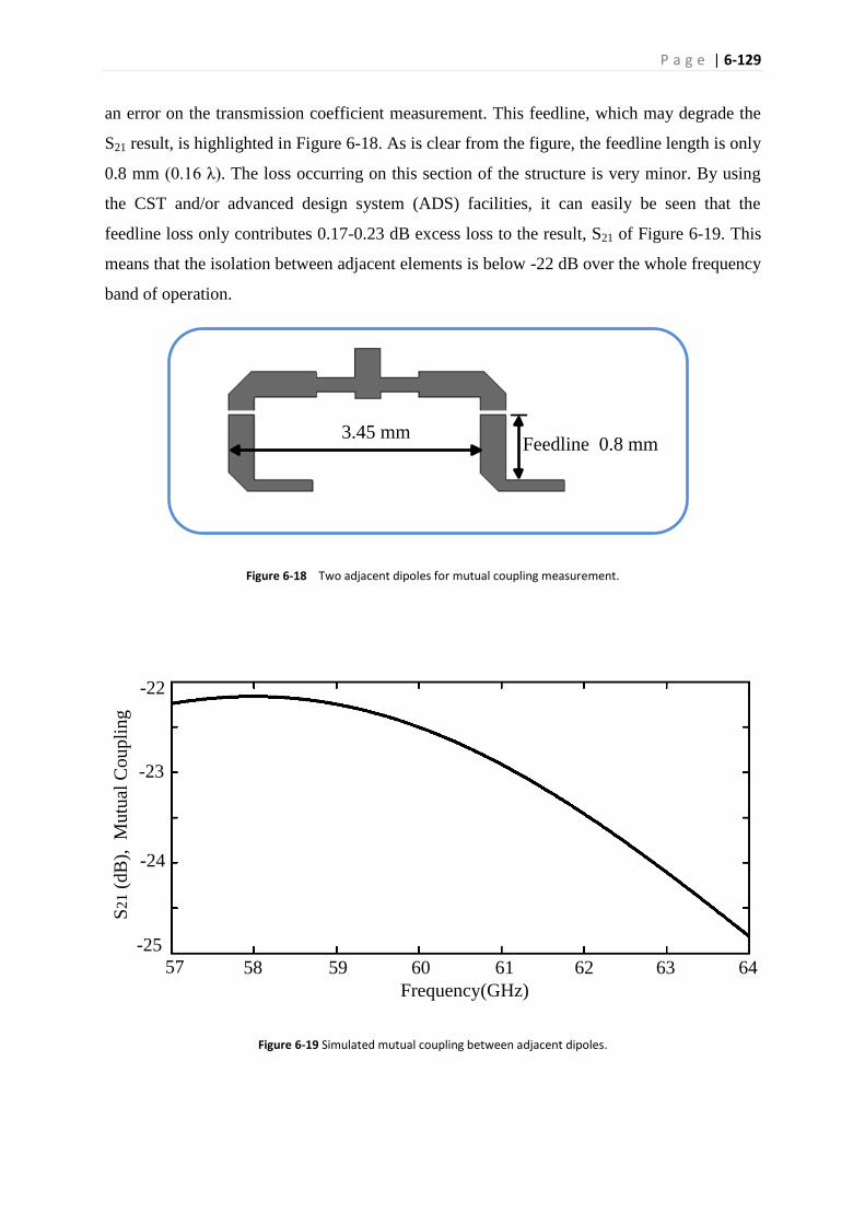
P a g e | 6-129
an error on the transmission coefficient measurement. This feedline, which may degrade the
S21 result, is highlighted in Figure 6-18. As is clear from the figure, the feedline length is only
0.8 mm (0.16 λ). The loss occurring on this section of the structure is very minor. By using
the CST and/or advanced design system (ADS) facilities, it can easily be seen that the
feedline loss only contributes 0.17-0.23 dB excess loss to the result, S21 of Figure 6-19. This
means that the isolation between adjacent elements is below -22 dB over the whole frequency
band of operation.
Figure 6-18 Two adjacent dipoles for mutual coupling measurement.
Figure 6-19 Simulated mutual coupling between adjacent dipoles.
3.45 mmFeedline 0.8 mm
S21 (
dB
), M
utu
al C
ou
pli
ng
Frequency(GHz)
57 58 59 60 61 62 63 64
-24
-25
-22
-23
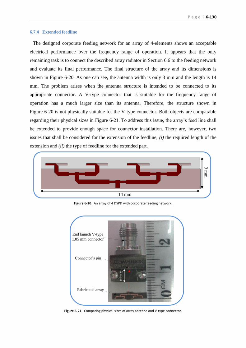
P a g e | 6-130
6.7.4 Extended feedline
The designed corporate feeding network for an array of 4-elements shows an acceptable
electrical performance over the frequency range of operation. It appears that the only
remaining task is to connect the described array radiator in Section 6.6 to the feeding network
and evaluate its final performance. The final structure of the array and its dimensions is
shown in Figure 6-20. As one can see, the antenna width is only 3 mm and the length is 14
mm. The problem arises when the antenna structure is intended to be connected to its
appropriate connector. A V-type connector that is suitable for the frequency range of
operation has a much larger size than its antenna. Therefore, the structure shown in
Figure 6-20 is not physically suitable for the V-type connector. Both objects are comparable
regarding their physical sizes in Figure 6-21. To address this issue, the array’s feed line shall
be extended to provide enough space for connector installation. There are, however, two
issues that shall be considered for the extension of the feedline, (i) the required length of the
extension and (ii) the type of feedline for the extended part.
Figure 6-20 An array of 4 DSPD with corporate feeding network.
Figure 6-21 Comparing physical sizes of array antenna and V-type connector.
14 mm
3 m
m
Fabricated array
Connector’s pin
End launch V-type
1.85 mm connector
5 m
m

P a g e | 6-131
The feedline length is bound by two contradictory factors. First, the shorter line is preferred
to minimise the loss occurring on the line and avoid unwanted radiation from the feedline.
This implies that a 5 to 7 mm extension is enough as shown in Figure 6-21. On the other
hand, however, the radiation pattern of the array shall be considered. As shown in
Figure 6-11, the dipoles have a noticeable back-lobe due to their configuration. If the array
antenna is placed very close to the connector, its back-lobe energy is reflected back to the
broadside direction by the connector structure. This may disturb the radiation pattern of the
array antenna. However, the major issue would be related to the increased level of the array
cross-polar level due to reflection of the V-type connector. As discussed earlier, the cross-
polar level is a critical parameter of the proposed antenna structure for the image-based
application. To minimise this effect, the length of the feedline is extended beyond what was
mandated by the physical requirements for connection purposes. As a trade-off selection for
the feedline length, 20 mm extension is selected equal to almost 4λ. This provides enough
distance between the connector and the array for minimum disturbance of the radiation
pattern and degradation of the cross-polar level. However, the loss occurring on the line shall
also be considered.
It is possible to simply extend the microstrip line, however, induced surface wave results in
higher loss. To reduce the effect of a long feedline on the antenna performance, the coplanar
waveguide (CPW) extension is used instead of a microstrip line. The grounded CPW line is
immune to surface wave and it also provides better robustness to the cooper roughness than
the normal microstrip line [150]. The prototype array is fabricated on Taconic, TLX-8 using a
photolithographic fabrication process. The photograph of the assembled array antenna with
extended CPW feedline and the V-type connector [151] assembly is shown in Figure 6-22.
Due to the very tiny dimension of the connector’s central pin, soldering would be very
difficult and may cause distortion in the element performance. Therefore, the central pin only
touches the feedline without any soldering.
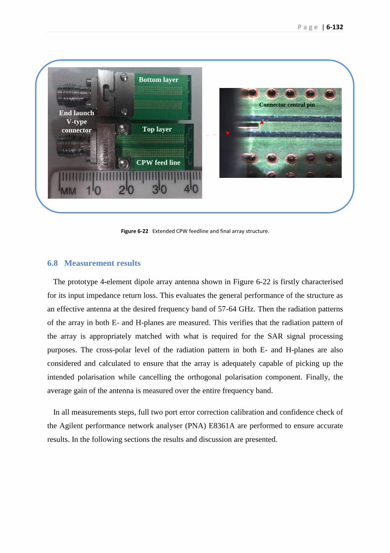
P a g e | 6-132
Figure 6-22 Extended CPW feedline and final array structure.
6.8 Measurement results
The prototype 4-element dipole array antenna shown in Figure 6-22 is firstly characterised
for its input impedance return loss. This evaluates the general performance of the structure as
an effective antenna at the desired frequency band of 57-64 GHz. Then the radiation patterns
of the array in both E- and H-planes are measured. This verifies that the radiation pattern of
the array is appropriately matched with what is required for the SAR signal processing
purposes. The cross-polar level of the radiation pattern in both E- and H-planes are also
considered and calculated to ensure that the array is adequately capable of picking up the
intended polarisation while cancelling the orthogonal polarisation component. Finally, the
average gain of the antenna is measured over the entire frequency band.
In all measurements steps, full two port error correction calibration and confidence check of
the Agilent performance network analyser (PNA) E8361A are performed to ensure accurate
results. In the following sections the results and discussion are presented.
Bottom layer
Top layer
End launch
V-type
connector
CPW feed line
Connector central pin

P a g e | 6-133
6.8.1 Reflection coefficient measurement
The designed array of four DSPD’s is simulated using CST Microwave Studio. However,
as discussed before, the V-type connector may have significant effect on the final
performance of the structure due to its large size at mm-wave range of 60 GHz. Therefore,
the connector is also included in the simulation process to provide a more accurate result. The
final structure, which is considered in CST is shown in Figure 6-23. Therefore, the effect of
the microstrip to CPW transition, the 20 mm long feedline and V-type connector assembly
are included in the simulations. The dimensions of the V-type connector are derived from its
data sheet [152], however, the material of the connector was unknown. Aluminium (lossy
metal) is assumed for the connector body and silver for its central pin. The fabricated antenna
through the photolithographic process shown in Figure 6-22 is connected to the Agilent PNA
for its return loss measurement after proper calibration of the system.
The simulated and the measured S11 in dB versus frequency are presented in Figure 6-24. It
is important to again emphasise that the simulated and measured return loss reflects the
effects of the array antenna, its long feedline, microstrip to CPW transition and the V-type
connector assembly. Three main aspects of the graphs in Figure 6-24 can be categorised as
follow:
i) Satisfactory return loss. As shown in Figure 6-24, both simulation and measured results
yield more than 10 dB return loss over the frequency band of operation with maximum RL of
more than 30 dB at 63 GHz. This ensures the satisfactory performance of the fabricated array
on the band 57-64 GHz. It also confirms that the effect of a long feedline and the connector
as well as the transition between microstrip to CPW, have been appropriately taken into
account.
ii) Minor simulation and measurement mismatch. The graphs in Figure 6-24 are not fully
matched to each other. Regarding the high frequency range of operation and also the
fabrication technique used, some minor mismatching would be normal. To have a better
understanding of the problem, the fabricated array is investigated thoroughly with a digital
microscope. The dimensions of the array in different sections are measured and compared
with the original values. The percentage of errors in various parts of the array is shown in
Figure 6-25. As one can see from Figure 6-25, errors in different parts of the structure have
significantly different values. While the width of the design is more vulnerable to errors, the
lengths of the various parts are more immune to fabrication errors. For example, while some
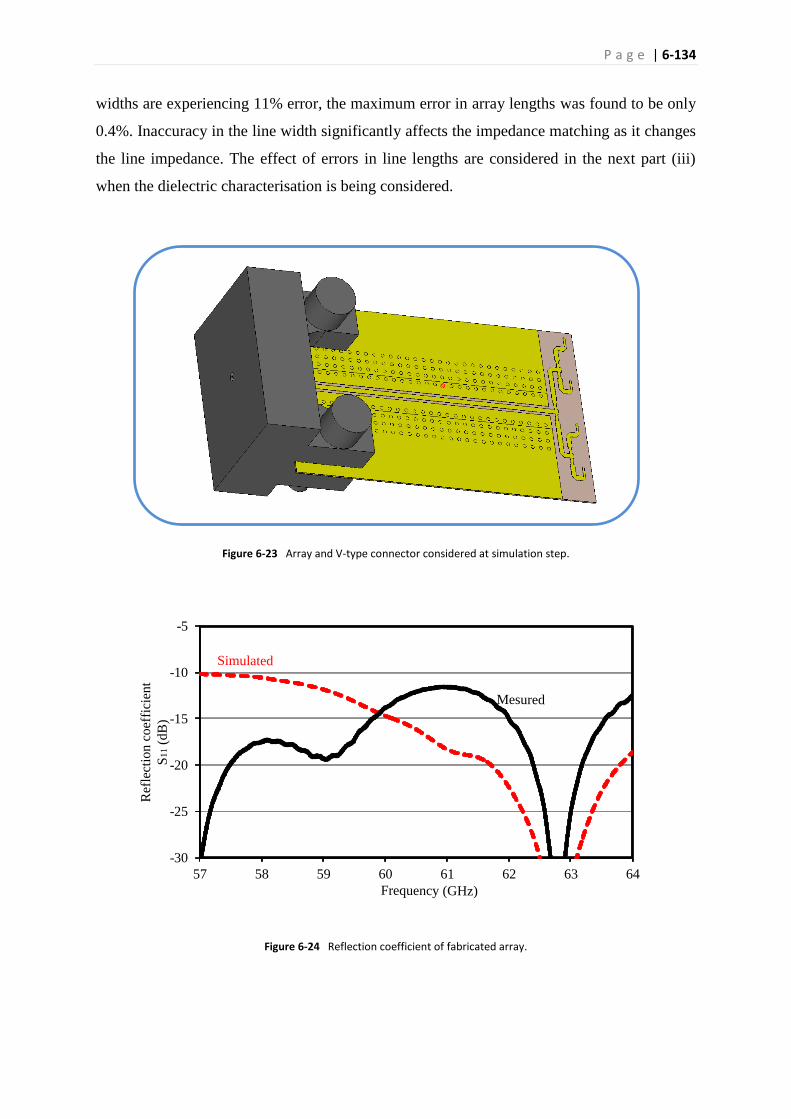
P a g e | 6-134
widths are experiencing 11% error, the maximum error in array lengths was found to be only
0.4%. Inaccuracy in the line width significantly affects the impedance matching as it changes
the line impedance. The effect of errors in line lengths are considered in the next part (iii)
when the dielectric characterisation is being considered.
Figure 6-23 Array and V-type connector considered at simulation step.
Figure 6-24 Reflection coefficient of fabricated array.
-30
-25
-20
-15
-10
-5
57 58 59 60 61 62 63 64
Frequency (GHz)
Ref
lect
ion
co
effi
cien
t
S1
1 (
dB
)
Mesured
Simulated

P a g e | 6-135
Figure 6-25 Percentage of errors in fabrication process.
Moreover to the errors occurring in the line widths, which result in impedance mismatch,
one may suspect that residual surface waves, in the extended via grounded CPW line, and V-
type connector assembly, cause impedance mismatch between the simulation and measured
results. However, more than 10 dB return loss over the frequency band ensures no significant
mismatch in the antenna and meets the specifications as discussed earlier.
iii) Accurate dielectric characterisation. The resonance frequency of the array is mainly
controlled by the length of the dipole arm and the dielectric constant. As shown in
Figure 6-24, the simulated resonance frequency and the measured resonance are both
concentrated around 63 GHz. This means that the simulation and measured results are
adequately matched from the resonance frequency perspective. As was already explored in ii)
that the lengths of the dipole’s arms are not significantly affected by the fabrication tolerance.
Therefore, having the same simulated and measured resonance frequency confirms the
accuracy of the dielectric characterisation method as described in Section 6.5.2. In other
words, the calculated mean value of the measured εr for the Taconic TLX-8 at 60 GHz
provides a good prediction of the used substrate performance at the 60 GHz frequency band.
6.8.2 Antenna fabrication error
At 60 GHz, the design would be very sensitive to any error during fabrication process. The
effect of fabrication error was shown in previous section where inaccurate widths in the array
feed network and dipole arms resulted in mismatch between the measured and simulated
reflection coefficient. For the proposed image based chipless RFID system, at least two array
antennas are required. However, the proposed technique may require more than 50 sets of
array as will be discussed in Chapter 8 for the fast imaging purpose. It is therefore important
to consider the design robustness to dimensional tolerances as process variation in
-3%
+9% +6%
+2.5%
-2.5%
+0.4%
+11%
Dipole arm

P a g e | 6-136
photolithographic etching always exists. Therefore, coordination with PCB manufacturing
vendors before finalizing the design is crucial. Based on the accuracy of the fabrication
process, it is normally required to re-tune certain parts of the design for better design
reliability. It was discussed earlier that the T-junction power divider provides higher
bandwidth when a reactive stub is utilised compared to a conventional V-notch in its structure.
Moreover, it was found that the reactive stub significantly influences the design robustness to
process errors while it also helps to broaden the element bandwidth.
Based on this finding, 5 samples of fabricated array antennas as shown in Figure 6-26 are
measured by a digital microscope. The sample photograph of the feed network is also shown
in Figure 6-26. The values of errors in different sections of the array structure is summarised
in Table 6-5. As it is clear from Table 6-5, the width of lines in the printed circuit is more
vulnerable to process error than the line length as discussed earlier.
Table 6-5 Fabrication variation
The measured input impedance, return loss (S11 in dB) vs frequency through PNA for five
fabricated array samples and the simulated S11 based on the accurate design values are shown
in Figure 6-27. While the measured return losses are not completely matched with the
simulation result due to the fabrication error, all five samples have acceptable performance
(S11>10 dB) in the frequency range 57-64 GHz. Moreover, one may notice all of the
fabricated samples acquire almost the same resonance frequency as suggested through
simulation, around 62.8-63.2 GHz. As all five samples have almost an accurate length of
dipole’s arms, see Table 6-5, therefore, the electrical parameters of the substrate was well
predicted through SIW approach as discussed in Section 6.5.2. It can also be concluded that
irrespective of fabrication error through conventional photolithographic PCB fabrication
technique, appropriate antenna design at 60 GHz mm-band is feasible.
Parameter Pw Da Pt Ig
Error(%) [-1.5, 3] [-0.2, 0.4] [-7, 11] [-3, 9]
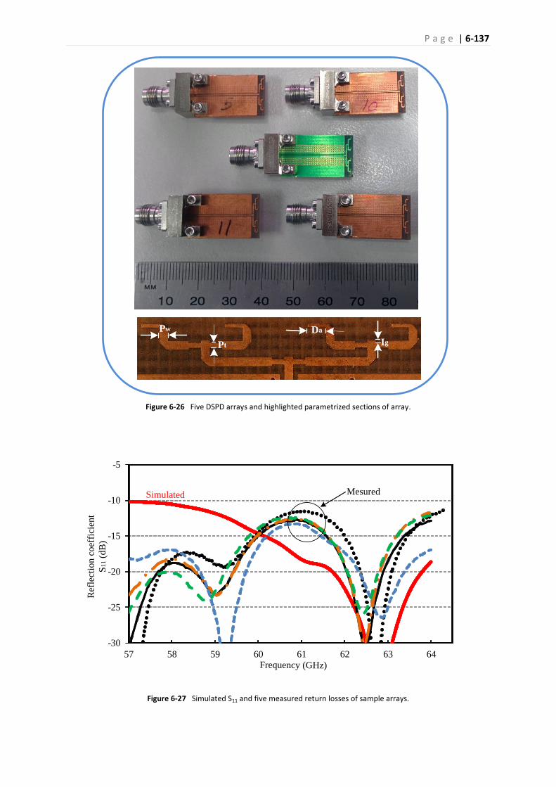
P a g e | 6-137
Figure 6-26 Five DSPD arrays and highlighted parametrized sections of array.
Figure 6-27 Simulated S11 and five measured return losses of sample arrays.
DaPw
Pt Ig
-30
-25
-20
-15
-10
-5
57 58 59 60 61 62 63 64Frequency (GHz)
Ref
lect
ion
co
effi
cien
t
S11 (
dB
)
Simulated Mesured

P a g e | 6-138
6.8.3 Radiation pattern measurement
After being satisfied with the performance of the array of DSPDs through input impedance
return loss measurement, the radiation patterns of the fabricated array are measured.
Figure 6-28 shows a photograph of the system measurement set up with the standard gain
horn antenna mounted on a fixed Perspex pole and the array antenna under test (AUT)
mounted on a turntable. The AUT is tested as a receive antenna and a horn antenna [153],
manufactured by Ainfoinc Inc., is used as a standard gain transmitting antenna. Agilent PNA
E8361A in its receiver mode is used. The distance between two antennas is sufficiently
higher than the farfield distances of the AUT and the horn antenna.
The radiation pattern is measured at every 10 step for a full 360 for both E- and H-plane
cuts. As the automatic measurement facilities were not available on the MMARS laboratory,
all measurements were completed manually. Some conical absorbers are placed around the
antennas to reduce surrounding interferences. Figure 6-29 shows the measured and simulated
co-polar and cross-polar radiation patterns at 58, 60 and 63 GHz for the E-plane. As one can
notice, the main beam of the pattern is well-focused. This is required to minimise reflections
from other objects around the tag and concentrate the radiated power on the tag surface. The
measured radiation patterns are congruent with the simulation results with minor shifts in
sidelobe levels. This can be seen as a good result considering the mm-wave range of
operation and the manual measurement process of the pattern.
Figure 6-28 System set up for radiation pattern measurement.
Standard horn antenna
Antenna under test (AUT)
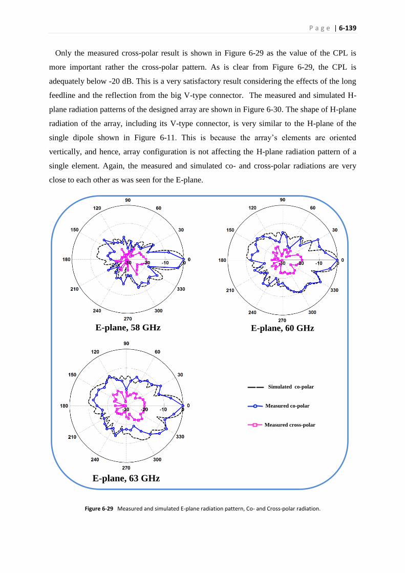
P a g e | 6-139
Only the measured cross-polar result is shown in Figure 6-29 as the value of the CPL is
more important rather the cross-polar pattern. As is clear from Figure 6-29, the CPL is
adequately below -20 dB. This is a very satisfactory result considering the effects of the long
feedline and the reflection from the big V-type connector. The measured and simulated H-
plane radiation patterns of the designed array are shown in Figure 6-30. The shape of H-plane
radiation of the array, including its V-type connector, is very similar to the H-plane of the
single dipole shown in Figure 6-11. This is because the array’s elements are oriented
vertically, and hence, array configuration is not affecting the H-plane radiation pattern of a
single element. Again, the measured and simulated co- and cross-polar radiations are very
close to each other as was seen for the E-plane.
Figure 6-29 Measured and simulated E-plane radiation pattern, Co- and Cross-polar radiation.
E-plane, 58 GHz E-plane, 60 GHz
E-plane, 63 GHz
Simulated co-polar
Measured co-polar
Measured cross-polar

P a g e | 6-140
Very minor difference between the two results specifically for angles above 30° is due to
the focused radiation of the standard horn antenna. This means that when the AUT is turned
around, it is slightly off the full illumination zone of the horn antenna and hence a little drop
in the measured signal strength has occurred. The wide radiation of the whole structure
including its connector, is essential for the appropriate usage of the designed array for
synthetic aperture signal processing. As discussed earlier, the array shall illuminate the tag
surface from different view angles, up to 60°, hence a constant radiation over a wide angle
is mandatory. Hopefully, the measurement result confirms that the fabricated array is capable
of providing such a wide radiation pattern over the azimuth direction. The measured H-plane
cross-polar radiation is also depicted in Figure 6-30. The value of the cross-polar level is
below -20 dB for the broadside direction. However, for some angles, it may increase to -18
dB. This can be noticed on the graphs of Figure 6-30 for angles 10° and 330° for cases 58 and
63 GHz. As is discussed in the next chapter, this doesn’t create any difficulty for separation
of the cross-polar component of the tag response from its co-polar reflections. Again it should
be mentioned that -20 dB cross-polar level on the H-plane is very well accepted for the
designed array considering the effects of the long feedline and reflection from the big V-type
connector.
Half power beamwidth (HPBW) of the array in its E- and H-plane quantitatively describes
the radiation pattern. Regarding the wide azimuth radiation pattern, the measured HPBW for
the H-plane would be acceptable in 10° measurement steps. However, for the E-plane
radiation pattern, the suggested 10° measurement setup does not provide the required
accuracy. For this purpose, it is therefore mandatory to measure the radiated power in more
accurate angles, 1° for example. The 1° step measurement for HPBW of the array in the E-
plane is shown in Figure 6-31. The re-measurement process for the E-plane is only repeated
for the 10° of the boresight direction. This would be enough to provide a more accurate
value of HPBW for the E-plane.
By considering the manual rotation of the AUT at every 1, small errors are expected. To
minimise this error, the measurement is repeated three times and the average value is
considered. Figure 6-32 shows the co-polar radiation pattern in 10 of the boresight
direction of the array antenna at 58 GHz. It shows that the measured HPBW is smaller when
compared with the simulated HPBW. This process is repeated for the other two sample
frequencies: 60 and 63 GHz. Table 6-6 summarises the HPBW of the array for both E- and

P a g e | 6-141
H-plane. It is important to notice that for the E-plane, the measurement accuracy is within 1°
while for the H-plane it is 10°. For all cases, the measured HPBW is smaller than the
simulation result.
Figure 6-30 Measured and simulated H-plane radiation pattern, Co- and Cross-polar radiation.
H-plane, 58 GHz H-plane, 60 GHz
H-plane, 63 GHz
Simulated co-polar
Measured co-polar
Measured cross-polar
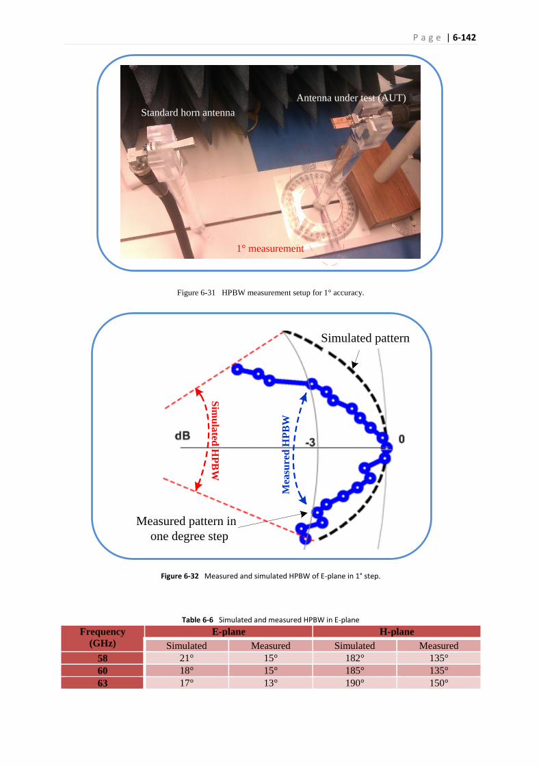
P a g e | 6-142
Figure 6-31 HPBW measurement setup for 1° accuracy.
Figure 6-32 Measured and simulated HPBW of E-plane in 1° step.
Table 6-6 Simulated and measured HPBW in E-plane
Frequency
(GHz)
E-plane H-plane
Simulated Measured Simulated Measured
58 21° 15° 182° 135°
60 18° 15° 185° 135°
63 17° 13° 190° 150°
Antenna under test (AUT)
Standard horn antenna
1° measurement
Mea
sure
d H
PB
W
Simulated pattern
Measured pattern in
one degree step
Sim
ula
ted H
PB
W

P a g e | 6-143
The measured values of the HPBW reflected in Table 6-6 for both the E-and H-plane
pattern adequately satisfy the required beamwidth of the array for the image-based chipless
RFID application as previously summarised in Table 6-1. However, there is a difference
between the measured value and the simulated HPBW for the H-plane. As mentioned before,
the measured signal level, for angles higher than 30° of boresight, experiences a drop as
the AUT is located a little off the illumination zone of the standard horn antenna. It is
possible to increase the reading range to avoid this error, however, the limited transmission
power of the PNA at a 60 GHz frequency range causes errors in the received signal level if
the reading range exceeds 25 cm. The current measured HPBW of the H-plane is still wide
enough ( > 115°) for the proposed application. Therefore, no further action was taken
regarding this measurement error.
6.8.4 Gain measurement
The final step of the array evaluation process is its gain measurement. It assures that the
antenna is capable of providing enough energy in the desired direction. To measure the gain,
a mixture of measurement, simulation and calculation is required and results shall be
combined to provide the gain of the array. Again the standard horn antenna is used as the
transmit antenna and the array, as the AUT receives the signal, while the Agilent PNA
measures the S21 of the transmission link. The gain of the array relates to other parameters of
the transmission link by:
21 Tx Rx Tx AUT cable FS FeedlineS P P G G L L L all in dB (6.9)
where GTx is the gain of the horn antenna,10.6 dBi [153]. Lcable is the PNA cable loss and shall
be measured directly by using full two port error correction calibration in the Agilent PNA
E8361A. In this process, the loss of connectors and adaptors are also considered. Free space
path loss, LFS, is calculated using the Friss transmission formula [144]. The required inputs
for the Friss formula are the distance and frequency. The feedline loss is required to be
separately considered as the CPW feed extension is 4λ long and contributes significantly to
the gain result. This loss has been separately simulated in CST and shown in Figure 6-33.
The 1.85 mm V-type Southwest microwave connector has VSWR of 1.25 [151]. This
means that the impedance mismatch of the connector should not have a big effect on the gain

P a g e | 6-144
measurement. Therefore the connector’s performance is not excluded from the gain
measurement. By considering (6.9) and by combining the measured data with the calculated
LFS and simulated Lfeedline, the final value of the gain versus frequency is shown in
Figure 6-34.
As can be seen from the figure, the feedline loss and the antenna gain are congruent to each
other over the whole frequency band. There is about 1.5 dB gain drop from 7 dBi due to 1.5
dB insertion loss variation of the feedline, 60-61 GHz. The absolute gain of the array antenna
varies from 5.5 - 7 dBi over the frequency band of operation as shown in Figure 6-34.
Figure 6-33 Simulated feedline loss of array.
Figure 6-34 Measured gain of array.
-2.3
-1.8
-1.3
-0.8
57 58 59 60 61 62 63 64
0.8
1.3
2.3
1.8
Frequency (GHz)
Fee
dli
ne
loss
(d
B)
0
2
4
6
8
10
57 58 59 60 61 62 63 64
Frequency (GHz)
Arr
ay g
ain
(d
B)
P a g e | 6-145
6.9 Conclusion
This chapter first has reviewed the technical and operational necessities of the reader
antennas for the proposed technique of the image-based chipless RFID system. Based on the
proposed application, the technical specifications of the reader antenna were stablished first.
A survey on the available open source products was conducted and their technical
specifications were reviewed, aiming to fulfil the required parameters. It was found that “off-
the-shelf” products on the mm-wave range of 60 GHz are not suitable for the demanded
specifications in the proposed technique.
When the actual demand for designing a new antenna set at 60 GHz was stablished, the
process of the antenna design was introduced. An array of double side printed dipoles (DSPD)
antennas was proposed to satisfy the demanded technical specifications. This part built the
basis of the further activities discussed in the rest of this chapter. A DSPD array antenna was
designed and thoroughly investigated at 60 GHz for the image-based chipless RFID tags. The
prototype antenna was design and fabricated on Taconic TLX-8.
First, the substrate was characterised using a SIW resonant technique. The measured
constitutive parameters of the Taconic TLX-8 at 60 GHz significantly differed from that of
published data at 10 GHz. The extract constitutive parametre data at 60 GHz was used for
designing a 4-element DSPD array antenna. In the process of the design, the following
advanced design techniques were used: (i) a broad band matching technique using dipole
arms chamfering and abrupt ground plane for the dipole element, (ii) element array analysis
and mitigating mutual coupling between elements, (iii) beam forming network with matching
stub at the T-junction, (iv) microstrip to CPW transition and SIW based CPW extensions and
finally, (v) a V-type connector assembly. The array of four DSPD elements covers the whole
frequency range of 57-64 GHz yielding 12% bandwidth. The array and its feeding network
were tuned to enhance the antenna performance. While the array dimension is very small and
the standard printed circuit board technology was used for the antenna fabrication, the
measurement results were well-matched with the simulation predictions. The antenna
provided a uniform radiation pattern in the azimuth direction with a limited pattern on the
elevation angle. The wide azimuth radiation pattern, H-plane, is suitable for the proposed
cross-polar RCS-based chipless RFID application due to its requirement for SAR signal
processing. The limited radiation in elevation angle, E-plane, also focuses the energy on the
tag surface and minimises the unwanted radiation. The measured CPL was below -20 dB.

P a g e | 6-146
This low CPL was required for proper operation of the image-based chipless RFID
applications. The measured gain of the array was 5.5-7 dBi over the entire frequency range of
operation. The size of the array was 22 14 mm2. The compact and simple structure of the
array also made it suitable for many applications in the mm-wave region for low range
wireless communication systems.
P a g e | 7-147
Chapter 7 EM-imaging
7.1 Introduction
EM-imaging fundamentals for data decoding of the chipless RFID system has already been
presented in Chapter 3. The EM-imaging is only feasible at mm-wave bands of 60 GHz and
higher frequencies, for the appropriate reading range, tag size, and expected data encoding
capacity. A single antenna at the 60 GHz band does not provide the required millimetre order
azimuth resolution, known as the foot print of antenna, at the normal reading distance of
chipless RFID systems due to the far field restriction. The SAR technique is proposed as a
solution for this purpose.
This chapter presents the SAR-based signal processing for the proposed chipless RFID EM-
imaging. First, the basics of EM-imaging are reviewed and the necessity for using the SAR
technique in different applications is discussed. It is shown that there are various applications
where the SAR approach has both practical and technical advantages over other imaging
techniques. The chipless RFID system is one of the applications for which the SAR is
necessary for the technical reasons.
Then the main modes of operation for the SAR technique are introduced. The spotlight
mode is highlighted due to its attributes for the proposed application in chipless RFID
systems. The technical details of the SAR technique are reviewed to establish a fundamental
basis for further steps in this chapter. The technical requirements for the transmit signal and
the system general structure are defined in this section.
The technically achievable range and cross-range (azimuth) resolutions using the SAR
technique are related to the technical parameters of the system in the next section. These
parameters are the frequency of operation, available bandwidth, and synthetic aperture size.
These parameters are then considered for the proposed chipless RFID application. The
practical range and azimuth resolutions are defined. The ultimate data encoding capacity of
the system is calculated based on the achievable resolution.
The appropriate data encoding algorithm is then discussed and a sample tag with only four
bits data capacity is considered for the proof of concept. It is shown that changing only one
bit of the tag data significantly changes the pattern of the received signal. Then the written
codes based on the simplified spotlight mode reveals the final EM-image of the tag’s encoded
data. This step confirms the applicability of the proposed technique at its last stage. The

P a g e | 7-148
effect of synthetic aperture size on the achievable EM-image is also studied and it is shown
that a minimum aperture size of 22 cm is required to decode the four bits tag at 10 cm reading
distance.
In the last section of this chapter, the ultimate encoding capacity of the proposed technique
is considered based on the maximum allowable tag surface. A tag that is 5.5 times smaller
than a credit card encodes 17 bits of data while it is fully printed by a SATO printer. This
suggests more than 93 bits on credit card size tag is possible. This is a revolutionary step
forward achieving EPC global standard from a mm-wave chipless RFID system.
7.2 SAR, an effective imaging algorithm
In this section, the SAR technique is briefly introduced and its main advantage on providing
a fine cross-range (azimuth) resolution is presented. Different modes of operation for the
SAR technique are defined and the appropriate mode for the chipless RFID system is
proposed.
7.2.1 SAR versus conventional systems
Radar is an acronym of “radio detection and ranging” [80] and it normally refers to the use
of EM-waves by the system. It is an important technology for military and civil applications.
The resolution of the radar system shows the ability of the system to separate multiple
scatterers in close proximity, known as the radar resolution. A 2-D resolution is normally
enough for the radar system [154], however, there are some advanced techniques for
providing 3-D information [80, 155, 156]. The two basic resolutions of the radar system are
the range and track-range resolutions. The range resolution is proportional to the utilised
bandwidth of the transmit signal. The track-range resolution is sometimes referred to as the
cross-range or azimuth resolution. In the rest of this dissertation, the azimuth resolution is
used. Azimuth resolution depends on the beamwidth of the radar antenna. A fine azimuth
resolution requires a larger radar antenna to provide a narrow beamwidth.

P a g e | 7-149
In many applications, the size of the radar antenna is restricted due to the various reasons,
hence, radar has a limited azimuth resolution. Carl A. Wiley introduced a new technique for
enhancing the azimuth resolution of the radar system through a small antenna with the
expense of complex signal processing [87, 154]. He proposed the use of a small antenna with
fairly wide beamwidth. The antenna moves around the target and illuminates it through
different angles. All the received signals are restored based on different radar positions. Then
the signal processing of the stored signals results in a very fine azimuth resolution which
normally requires a much larger antenna aperture than that of the actual utilised antenna.
Figure 7-1 shows the transition from a conventional radar system to a SAR-based system.
Figure 7-1(a) presents a conventional radar antenna with large aperture size. This antenna can
be replaced by an array antenna with large number of elements. The higher the number of
elements, the more similar two antennas in Figure 7-1 (a) and (b) are. Based on the size of the
antenna in Figure 7-1(a) and the frequency of operation, thousands of elements may be
required in Figure 7-1(b). Instead of utilising a large number of elements, SAR technique
suggests to use only one element and sequentially move it to different positions in the array
configuration. By restoring the received signal in each individual position, the effect of array
antenna with thousands of elements, Figure 7-1(b), or equivalently the effect of the real
antenna in Figure 7-1(a) can be successfully constructed.
Figure 7-1 Evolution of conventional radar toward SAR system through array antenna concept.
A conventional
reflector antenna
The equivalent real
array antenna
The equivalent SAR system
Active
element
LL
L
a) b)
c)

P a g e | 7-150
7.2.2 SAR modes of operation
SAR-based systems may work in different modes of operation which depends on the
system flexibilities and the application requirements. Three main modes of operations are:
i) spotlight, ii) strip map and iii) scan mode [154]. In the spotlight mode, the radar system
steers its antenna towards a certain area in which the target is located. The spotlight mode is
normally used when the target area is small and a fine image resolution of the target is
required. In the strip map mode, the radar antenna is fixed with respect to the system and the
moving route. These two modes of operation are shown in Figure 7-2. The strip map mode is
useful for providing a coarse-image resolution of a large area of interest, earth imaging for
example. If these two modes are combined, then the SAR system works on the scan mode.
The azimuth resolution provided by any mode of the SAR system directly depends on the
length of the synthetic aperture size. In the strip map mode, the synthetic aperture length is
fixed as the radar antenna has a fixed angle with the airplane. On the other hand, the spot
light mode does not experience any limitations on its synthetic aperture length as the system
has the ability to steer the beam of the physical antenna and illuminate the scene for a longer
period.
Figure 7-2 SAR modes of operation: a) Spotlight mode, b) Stripmap mode.
Synthetic aperture,
Fixed
Synthetic aperture,
Variable
Target scene
Target terrain
a) b)

P a g e | 7-151
For the proposed mm-wave chipless RFID tag, the maximum area the tag occupies is less
than a credit card size (85 × 55 mm2). On the other hand, the maximum azimuth resolution is
desirable as it defines the tag’s data encoding capacity. Therefore, the spotlight mode of SAR
seems to be an appropriate mode of operation for the RFID tag imaging. Through the
curvature nature of the reader route around the tag, it is possible to focus the radiation pattern
of the reader antenna on the tag surface and illuminate the tag through different view angles.
Moreover, flexibility on the length of the synthetic aperture size at the spotlight mode results
in finer azimuth resolution at the expense of a larger synthetic aperture length. This trade-off
between the aperture size and the image resolution is discussed in Section 7.6.2 with
measurement results. Figure 7-3 shows the system set up of the tag imaging process that is
very similar to the spotlight mode in Figure 7-2.
Figure 7-3 Spotlight mode of operation for finer azimuth resolution of chipless RFID tag.
ReaderReader
Rea
din
g r
ang
e
Synthetic aperture
RX
TX
RX
TX

P a g e | 7-152
7.3 SAR for chipless RFID
This section reviews the fundamentals of the SAR system and introduces basic expression
describing the spotlight mode as the appropriate mode of operation for the proposed RFID
application. Based on the expression derived in this section, the technical specification of the
proposed RFID system is defined. Finally, the system capabilities on range and azimuth
resolutions are determined.
7.3.1 SAR block diagram
The block diagram of a typical SAR-based system is shown in Figure 7-4. The radar
antenna provides real time data of the scene. In many cases, the information about the
movement of the radar system is collected during the operation of the system. These two sets
of data provide the scene data as well as the complementary data of the radar motion. The
image formation processor uses these two data sets to provide the SAR imagery to the image
processor and subsequently to the image exploitation segment [154]. For many applications,
including the earth imaging, the movement of the radar system is almost a fixed path,
however due to unexpected factors like wind and the terrain of the earth, small variations of
the radar route often happen. Therefore, the motion sensor is an unavoidable part of the
system. For the RFID application, however, the movement is completely predictable as the
radar moves on a rail. Therefore, this section can be ignored, while the information of the
route would be easily considered in the subsequent modules mathematically. The detailed
description of the modules in Figure 7-4 are described in [154].
Figure 7-4 General block diagram of typical SAR-based system [154].
Radar sensor
Image
formation
processor
Image
processor
Image
exploiting
segment
Motion sensor
Signal data
Radar motion
data
SAR imageryScene
information

P a g e | 7-153
7.3.2 Range resolution
The synthetic aperture concept improves the azimuth resolution of the system only. The
achievable azimuth resolution through the SAR technique is normally much better than that
possible with a single antenna. Therefore the SAR concept is very commonly used when the
size of the single antenna is limited due to technical reasons. However, accessing the same
range and azimuth resolutions is normally required in many applications. Therefore, the fine
azimuth resolution due to the SAR technique provides an incentive for utilising higher
bandwidth signals for fine range resolution as well.
The radar’s ability to separate two targets in range is known as range resolution. Based on
the signal type used in the transmit section of the radar, the range resolution may vary. For a
single short pulse, the radar can distinguish two adjacent targets in range, if the separation
time between their echoes is more than the pulse width. The range resolution, ρr, is the
minimum distance between two adjacent targets separated by the radar and is defined by:
/ 2r pcT (7.1)
where c is the speed of light and Tp is the pulse width. Figure 7-5 illustrates the range
resolution. Expression (7.1) is only valid if the targets and the radar system are in line as
shown in Figure 7-5.
With a fine range resolution, shorter pulses are needed. However, to maintain a satisfactory
average power level, high power pulses are required. There high power narrow pulses are
difficult to generate. This means that narrower pulses, that are required for finer range
resolution, contradict the requirement of a higher average transmitted signal for maintaining
the minimum signal to noise ratio (SNR) for a fixed reading range. To satisfy both
requirements, it is possible to have long, phase-coded pulses, which can be compressed with
a signal processing operation after reception. In this scenario, a linear FM signal, known as
the chirp signal, is transmitted during a long enough time as a pulse signal to satisfy the
minimum transmission power requirement. However, signal processing after reception
provides a fine resolution corresponding to a very narrow pulse shape.
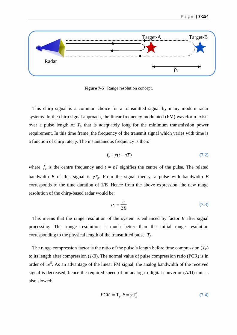
P a g e | 7-154
Figure 7-5 Range resolution concept.
This chirp signal is a common choice for a transmitted signal by many modern radar
systems. In the chirp signal approach, the linear frequency modulated (FM) waveform exists
over a pulse length of Tp that is adequately long for the minimum transmission power
requirement. In this time frame, the frequency of the transmit signal which varies with time is
a function of chirp rate, γ. The instantaneous frequency is then:
( )cf t nT (7.2)
where cf is the centre frequency and t = nT signifies the centre of the pulse. The related
bandwidth B of this signal is γTp. From the signal theory, a pulse with bandwidth B
corresponds to the time duration of 1/B. Hence from the above expression, the new range
resolution of the chirp-based radar would be:
2
r
c
B (7.3)
This means that the range resolution of the system is enhanced by factor B after signal
processing. This range resolution is much better than the initial range resolution
corresponding to the physical length of the transmitted pulse, Tp.
The range compression factor is the ratio of the pulse’s length before time compression (TP)
to its length after compression (1/B). The normal value of pulse compression ratio (PCR) is in
order of 1e5. As an advantage of the linear FM signal, the analog bandwidth of the received
signal is decreased, hence the required speed of an analog-to-digital convertor (A/D) unit is
also slowed:
2 T T p pPCR B (7.4)
ρr
Target-A
Radar
Target-B

P a g e | 7-155
The assumption of having the radar system and the targets in one line is not always
practically valid. In fact, in many applications, the radar has a slant view angle to the target,
Earth imaging, for example. In this case, (7.3) and (7.4) are equivalently not showing the
final range resolution of the system. Instead, the final range resolution known as the ground
range resolution could be easily found from its equivalent slant range resolution through:
rgr
Sin
(7.5)
Where, ρgr is the ground range resolution that is the final resolution of the radar system on the
target scene and ρr is the slant range resolution derived from (7.3) and (7.4).
Figure 7-6 clearly shows these two range resolutions. For the RFID application, the same
scenario is valid. The reader antenna is at 90° towards the tag’s surface. Meander lines are
located at close proximity of each other, 1 mm for example. The reading range is in the
10~50 cm range based on the maximum transmitted power of the reader. The required signal
bandwidth for these parameters based on (7.4) and (7.5) is in hundreds of GHz that is
technically impractical to achieve.
Figure 7-7 shows the slant and ground range resolutions for the chipless RFID application.
The front and side views of the tag are shown in Figure 7-7 along with the nominal
parameters of the reading scenario. Therefore, it can be concluded that providing the fine
range resolution of few millimetres on the tag surface is not possible due to the limited
available frequency band of operation. Hence the range resolution has no benefit for data
encoding purposes on the chipless RFID tag.
7.3.3 Azimuth resolution
The signal processing technique that SAR-based systems use to achieve a fine azimuth
resolution is the feature that distinguishes the SAR-based systems from other imaging
techniques [154, 157]. Synthetic aperture processing in azimuth exploits the linear FM
modulation that the quadratic variation in range to a target introduces as the radar passes. The
processor is able to compress this modulated azimuth signal to generate the resolution
associated with a narrow beamwidth from a wide beamwidth antenna [154]. In a radar
system, the radiation pattern of the radar antenna illuminates a cell and the presence or
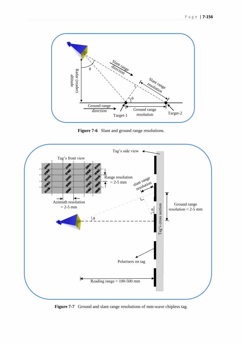
P a g e | 7-156
Figure 7-6 Slant and ground range resolutions.
Figure 7-7 Ground and slant range resolutions of mm-wave chipless tag.
Slant range direction
Slant range resolution
Ground range
resolution
Ground range
direction
θ Rad
ar (reader)
altitud
e
θ
Target-1Target-2
θ
Ground range
resolution ≈ 2-5 mm
slant ra
nge
resolution
Polarisers on tag
Tag
’s c
ross
sec
tio
n
θ
Tag’s front view
Tag’s side view
Reading range ≈ 100-500 mm
Range resolution
≈ 2-5 mm
Azimuth resolution
≈ 2-5 mm

P a g e | 7-157
absence of any target(s) is discovered by the backscattered signal. Two targets can be
distinguished if their angular separation is greater than the radar beamwidth. This means that
radar is not able to resolve targets which are closer to each other than the radar beamwidth.
The 3-dB beamwidth of an un-weighted antenna relates to its physical size (D) and frequency
of operation (λ) by [144]:
0.89aD
(7.6)
If the target is located at distance R, then the azimuth resolution of the radar is:
.
0.89a
R
D
(7.7)
For many applications the long distance of a target to the radar system (R) results in very
coarse azimuth resolution. Increasing the azimuth resolution is restricted by the maximum
allowable size of the antenna, D, in Earth imaging for example. In a SAR system, a small
antenna, D, moves over a large path known as synthetic aperture antenna length, L, and
illuminates the target scene with its wide beamwidth. The received signal at each individual
position of the real antenna is added coherently with the proper phase adjustment to maintain
the large synthetic aperture which yields a narrow beamwidth after proper signal processing.
This means that physically scanning the target scene through a small antenna with a wide
radiation pattern is equivalent to scanning the target scene with a much narrower radiation
pattern in the processor.
For the chipless RFID application, the relation between the required synthetic aperture
length and achievable azimuth resolution based on various reading ranges, R, is shown in
Figure 7-8. As one can easily see, the necessary length of the synthetic aperture is completely
practical to achieve the azimuth resolution of few millimeters. For example, in 15 cm reading
distance, a 20 cm synthetic aperture is enough to provide less than 4 mm azimuth resolution
on the tag surface. A 25 cm synthetic aperture length is normally enough to provide the
azimuth resolution of less than 5 mm for a reading range up to 25 cm. As can be seen later in
this chapter, the implementation of the system and the achieved image resolution confirms
the values of the graphs in Figure 7-8. This means that although the range resolution of few
millimetres requires huge spectrum bandwidth; the azimuth resolution is quite practical, and
proposes a new method for data encoding on a chipless tag with noticeable data capacity. The
implementation of the synthetic aperture radar theory for the chipless RFID is shown in this
chapter.

P a g e | 7-158
Figure 7-8 Azimuth resolution and required synthetic aperture length.
7.4 Tag structure for practical data encoding approach
As was already discussed the presence or absence of EM-polarisers on the tag surface,
meander lines for example, conveys the encoded data to the reader. To detect the existence of
the polarisers on the tag surface, the SAR EM-imaging is utilised. The provided image
resolution using the EM-imaging technique reveals the final data encoding capacity of the
system. If the tag surface is divided into a number of pixels, then each pixel may contain one
EM-polariser as the data encoding unit. The presence and absence of polariser represents the
“1” or “0” data respectively and hence carries one binary data bit. The size of the pixel on the
tag surface governs the final data encoding capacity of the tag. The finer the pixel, the higher
the data encoding capacity is. Figure 7-9 shows the pixelated tag surface. The width of the tag
has m pixels and its length is divided into n pixels. Without losing generality, it is assumed
that the pixels are square. This means that the tag surface comprises a matrix of m × n pixels.
As each pixel carries one bit of data, hence the total data encoding capacity is 2mn
. It was
already shown in Figure 7-8 that the resolution of the EM-imaging is in millimetre order, 3
mm for instance. Therefore, the theoretical data encoding capacity of the proposed technique
can be one bit in every 9 mm2
or equivalently more than 10 bits/cm2. This would be a
revolutionary data encoding capacity for a chipless RFID tag [158].
R=25 cm
R=20 cmR=15 cm
R=10 cm
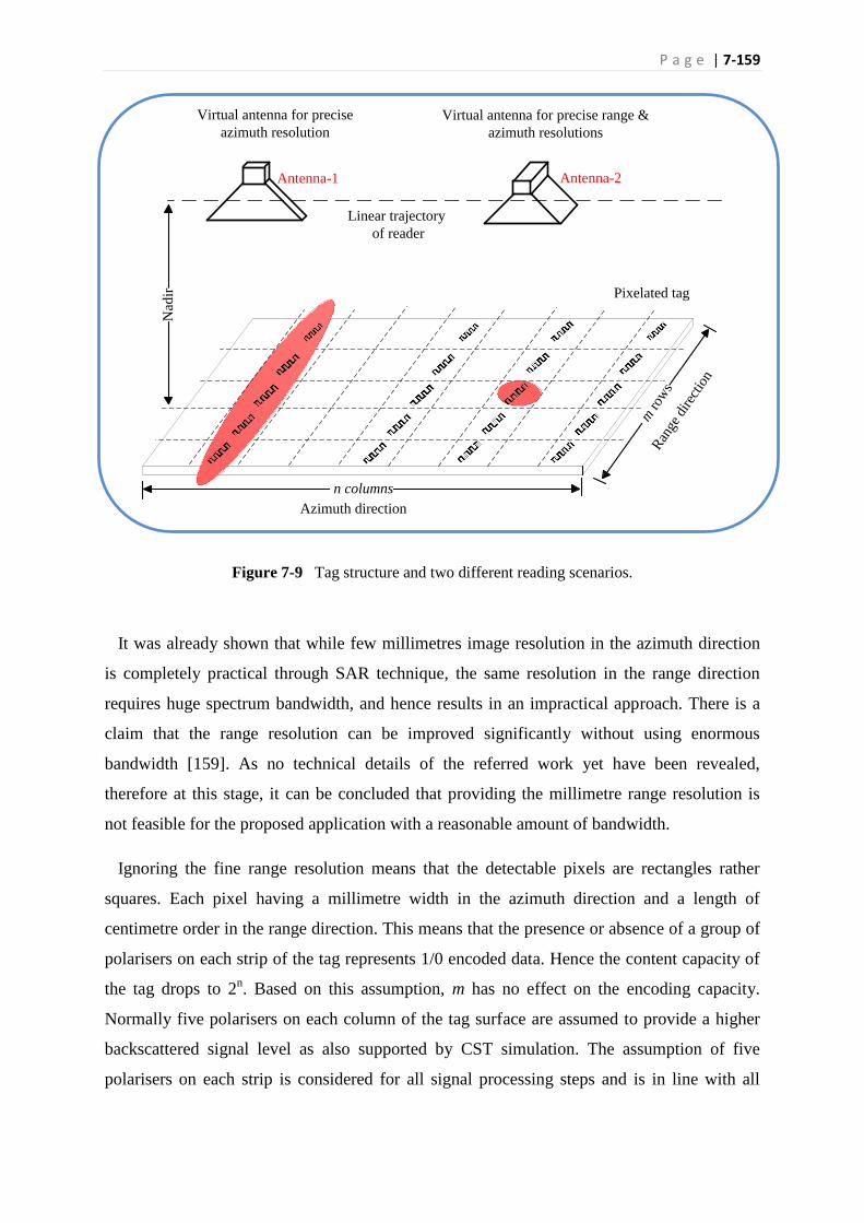
P a g e | 7-159
Figure 7-9 Tag structure and two different reading scenarios.
It was already shown that while few millimetres image resolution in the azimuth direction
is completely practical through SAR technique, the same resolution in the range direction
requires huge spectrum bandwidth, and hence results in an impractical approach. There is a
claim that the range resolution can be improved significantly without using enormous
bandwidth [159]. As no technical details of the referred work yet have been revealed,
therefore at this stage, it can be concluded that providing the millimetre range resolution is
not feasible for the proposed application with a reasonable amount of bandwidth.
Ignoring the fine range resolution means that the detectable pixels are rectangles rather
squares. Each pixel having a millimetre width in the azimuth direction and a length of
centimetre order in the range direction. This means that the presence or absence of a group of
polarisers on each strip of the tag represents 1/0 encoded data. Hence the content capacity of
the tag drops to 2n. Based on this assumption, m has no effect on the encoding capacity.
Normally five polarisers on each column of the tag surface are assumed to provide a higher
backscattered signal level as also supported by CST simulation. The assumption of five
polarisers on each strip is considered for all signal processing steps and is in line with all
Pixelated tag
Virtual antenna for precise
azimuth resolution
Virtual antenna for precise range &
azimuth resolutions
Linear trajectory
of reader
Nad
ir
m row
s
n columns
Azimuth direction
Ran
ge d
irec
tion
Antenna-1 Antenna-2

P a g e | 7-160
measurements that have been completed and shown in previous chapters. Therefore in this
new scenario, the tag’s width that corresponds to m is fixed. As every column of the
polarisers on the tag surface represents one bit of data, then the content capacity is
proportional to the tag length. When the moving reader finishes a full synthetic aperture
scanning, the effect of each strip of the tag is separately analysed after SAR-based signal
processing. Based on the presence or absence of the polarisers, the reader then receives
significantly different cross-polar power levels that can be used in the decoding algorithm.
In Figure 7-9 two virtual antennas are shown for two different scenarios. It is important to
note that these two antennas are just for representation purposes and there is not any
physically large antenna on the reader. Antenna-2 in Figure 7-9 represents the case when a
SAR-based reader moves around the tag and simultaneously utilises a very short pulse signal
with significant bandwidth. The reader is capable of providing a very fine image resolution in
both range and azimuth directions. The equivalent antenna would be a large horn antenna that
requires massive aperture in both sides. Antenna-1 in Figure 7-9 shows the equivalent horn
antenna for a reader system that only utilises the benefits of the SAR technique with a limited
bandwidth of the transmitted signal. This system is only capable of providing a fine azimuth
resolution. The provided range resolution for antenna-1 is very coarse in comparison to its
azimuth resolution. Therefore, the equivalent virtual horn antenna has an extended aperture in
the azimuth direction and limited size in the range direction. As discussed earlier, this is the
practical scenario for the current situation of the research. It is possible to propose a planar
movement of the reader in both direction and hence provide fine image resolution in both
directions. However at this stage, only the fine azimuth resolution through the movement of
the reader antenna in one direction is considered.
The data encoding capacity of the system with only azimuth resolution is accommodated to
the new rectangle shape of the pixels on the tag surface. Each pixel is 5 × 10 mm2 with one
bit of data encoding capacity. Hence, the equivalent data capacity is 2 bits/cm2. This data
encoding capacity is still very attractive for a fully printable chipless RFID tag with high
system robustness towards multipath interferences.

P a g e | 7-161
7.5 SAR-based signal processing
In this section, the EM-image of the tag is derived through the described SAR technique.
The tag is comprised of five meander lines as EM-polarisers in each column for data
encoding purposes. As discussed in the previous section, a fine azimuth resolution is only
targeted through the SAR technique. No attempt is made on range resolution because of the
limited available frequency spectrum. Presence of five EM-polarisers on each column of the
tag surface represents a binary data of “1” and no polariser means “0”. The measured cross-
RCS of each strip reveals the presence or absence of meander lines as the data encoding
algorithm.
The signal processing fundamentals are based on the SAR technique for azimuth resolution
and the range migration algorithm (RMA) for range resolution as described in [154].
Moreover, Charvat [81] simplified the proposed approaches in [154] for low range radar
systems. He has suggested a practical and low cost radar system with image resolution of
decimetre order. The current work follows the Carrara [154] and Charvat [81] approaches and
techniques with appropriate modifications for the proposed application of the chipless RFID
systems in mm-wave band.
7.5.1 System structure for data collection
The structure of the tag for EM-imaging is shown in Figure 7-9. The described antenna in
Chapter 6, which covers the frequency band 57-64 GHz moves on a straight line around the
tag. The straight line is assumed for simplicity of the signal processing. However, for the
final stage, the curved trajectory as shown in Figure 7-3 shall be considered. The curved path
provides better azimuth resolution as it uses the benefits of the spotlight mode of SAR
operation. The reading range, the nadir in Figure 7-9, may vary from 10-25 cm. However, all
the result shown in this chapter is based on 10 cm reading distance. This reading range is in
line with all measurements carried out so far and shown in previous chapters. The reading
step of the reader antenna is 2 mm that is equivalent to almost 0.4λ. This means that the
reader illuminates the tag surface in every 2 mm and collects its backscattered signal, and
then moves to the next position. The synthetic aperture size may vary from 20-35 cm.
However for 10 cm reading distance, the length of 20 cm is normally assumed for the
synthetic aperture size to achieve 5 mm azimuth resolution.
P a g e | 7-162
Considering the above mentioned parametres, the reading process of the tag requires a high
number of separate transmissions and receptions of the signal for data collection purposes;
125 steps for a 25 cm aperture size, for example:
250
1252
Aperture size mmNumber of reading
reading step mm (7.8)
This seems to be very slow as the reader has many stops for data measurement. This
limitation can be easily compensated through continuous movement of the reader through a
servo motor. In this case, the Doppler frequency shift due to the continuous measurement
process shall be also considered. There is software available, which considers the effect of the
Doppler frequency shift in signal processing [160-162]. The second approach for
compensation of the long reading process is introduced in the next chapter. In that approach,
no reader movement is required, hence the reading process can significantly speed up.
For the range resolution, a normal chirp signal with FM modulation is assumed. The chirp
rate of 400 GHz/sec, that is a nominal value for a chirp signal generator, is considered. At the
mm-wave band, the start frequency of 58.2 GHz and stop frequency of 62.2 GHz are
assumed. The pulse duration is 10 milliseconds hence the occupied frequency band of the
chirp is 4 GHz. Considering (7.4), one may expect a very coarse range resolution in multi
centimetre order. This is a much rough resolution when compared with azimuth resolution.
This means that the effect of all five meander line polarisers on each strip of the tag surface
are combined and cannot be separated by the reader.
7.5.2 Signal processing steps
As mentioned earlier, the RMA algorithm defined in [154] is followed for the SAR-based
coding. The captured data based on various positions of the reader antenna, known as the raw
signal, is processed by the RMA SAR-based algorithm. The RMA normally is divided into
the following separate steps:
- Data collection,
- Azimuth Fourier transform,
- Matched filter,
- Stolt interpolation,

P a g e | 7-163
- Inverse Fourier transform, and
- Reflectivity image
When the reader moves around the tag, in each specific position, a 2-D data matrix is
produced which contains the range profile data. Hence, the collected data has the formation:
, ( )iS x w t (7.9)
where xi contains the information of the reader position and the w(t) is the instantaneous of
the chirp signal and defines by (7.10) while the cr is the chirp rate, fc is the centre frequency
of the signal and BW is the signal bandwidth:
( ) 22
r c
BWw t c t f
(7.10)
The matrix format of (7.9) is considered as the raw signal by the codes for SAR-based
signal processing. In the RMA approach, the azimuth Fourier transformation is applied to this
raw signal. This is the first difference between the RMA and other conventional approaches
in SAR-based signal processing, polar formation algorithm for example. The Fourier
transformation changes the time-domain signal, S(xi,w(t)), to its equivalent wave number
domain, S(kx ,kr).
The next phase of the RMA is application of a 2-D phase compensation to the azimuth-
transformed signal [154]. This operation perfectly corrects the range curvature of all
scatterers at the same range as the scene centre. The matched filter is defined through the
following expression on which the Rs shows the distance between to the target centre [81,
154]:
2 2( , ) sjR
mf x r r xS k k e k k (7.11)
Following the matched filter step, Stolt interpolation is applied in the RMA algorithm. It
simultaneously compensates the range curvature of all scatterers by an appropriate wrapping
of the SAR signal data. This means that the 2-D SAR data from the wave number domain
(kr) to the spatial wave number domain ky through the following expression [154]:
2 2
y r xk k k (7.12)
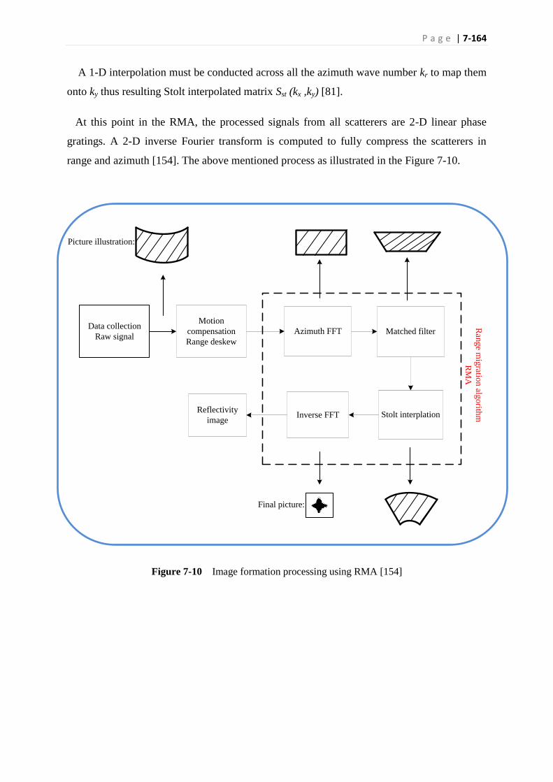
P a g e | 7-164
A 1-D interpolation must be conducted across all the azimuth wave number kr to map them
onto ky thus resulting Stolt interpolated matrix Sst (kx ,ky) [81].
At this point in the RMA, the processed signals from all scatterers are 2-D linear phase
gratings. A 2-D inverse Fourier transform is computed to fully compress the scatterers in
range and azimuth [154]. The above mentioned process as illustrated in the Figure 7-10.
Figure 7-10 Image formation processing using RMA [154]
Motion
compensation
Range deskew
Azimuth FFT Matched filter
Stolt interplationInverse FFTReflectivity
image
Data collection
Raw signal
Ran
ge m
igratio
n alg
orith
m
RM
A
Picture illustration:
Final picture:
P a g e | 7-165
7.6 Results
The measurement set up is similar to what explained in Chapter 4. Two sets of the designed
array of DSPDs antennas introduced in Chapter 6 are used as Tx and Rx antennas. They are
connected to the VNA while oriented orthogonally. The printed tag with a SATO printer is
located at 10 cm distance of the antennas. The reading distance of 10 cm is considered in all
of the measurements in this section because of restricted output power of VNA. At the
frequency band 57-64 GHz, the maximum levelled power of VNA is -5 dBm. Considering
the maximum gain of array antenna, 7.5 dBi, the EIRP of the system is only 2.5 dBm.
However, it has been mentioned in Chapter 3 that the maximum EIRP of 40 dBm is allowed
in this band [31, 32]. Therefore, the reading distance may increase to at least 50 cm in
commercial phase of the proposed EM-image chipless RFID system if a higher power signal
source is available at 60 GHz.
7.6.1 Proof of concept
Considering the proposed system structure and its related technical parameters, two tags
with different encoded data are considered. To prove the concept of the data decoding
through EM-imaging, the tags only include four bits of data, “1001” and “1011”. The tags are
2 cm long while their width is fixed to almost one cm comprising five meander line in each
column. A sample tag with four-bits of data is shown in Figure 7-11.
These two tags are interrogated through the reader at different angles while the reader
moves on a straight line of 22 cm. It is important to note that the length of synthetic aperture
is 20 cm; however to scan the total tag’s surface it is required to add the length of the tag to
the initial synthetic aperture length. As mentioned in the previous section, the reader utilises 4
GHz bandwidth. The received signal before SAR-based signal processing, the raw signal, is
shown in Figure 7-12 and Figure 7-13. Based on the position of the reader, various power
levels are detected that depend on the frequency of operation. The power levels shown in
Figure 7-12 and Figure 7-13 are the normalised power for two tags “1001” and “1011”,
respectively. The raw signals shown in Figure 7-12 and Figure 7-13 convey no information
at this moment, hence the steps mentioned in Section 7.5.2 shall be taken to extract the tag
information. However, comparing the two figures reveals that only changing one bit of the
tag’s data completely changes the pattern of the received signal.
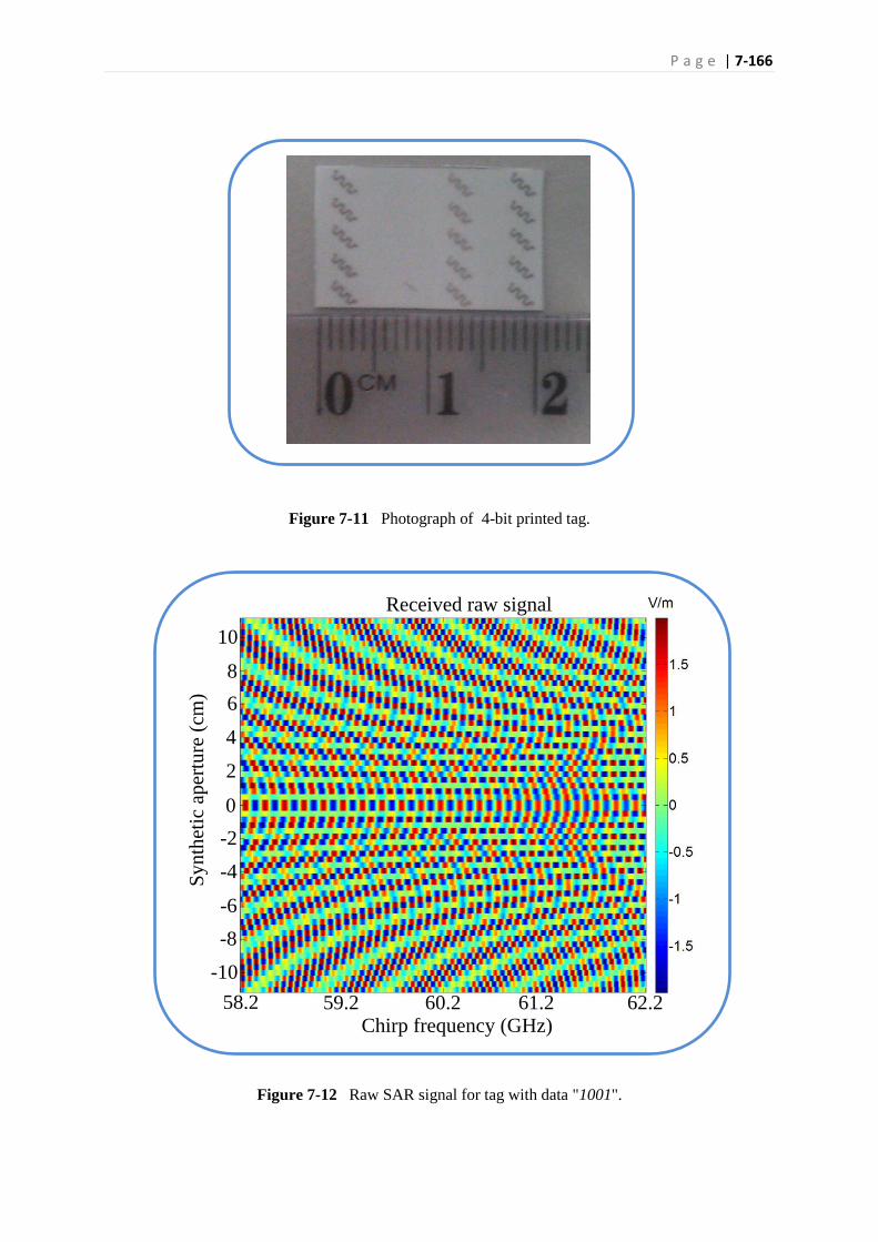
P a g e | 7-166
Figure 7-11 Photograph of 4-bit printed tag.
Figure 7-12 Raw SAR signal for tag with data "1001".
58.2 59.2 60.2 61.2 62.2
0
-2
-10
-8
4
10
6
Sy
nth
etic
ap
ertu
re (
cm)
Chirp frequency (GHz)
Received raw signal
8
2
-4
-6
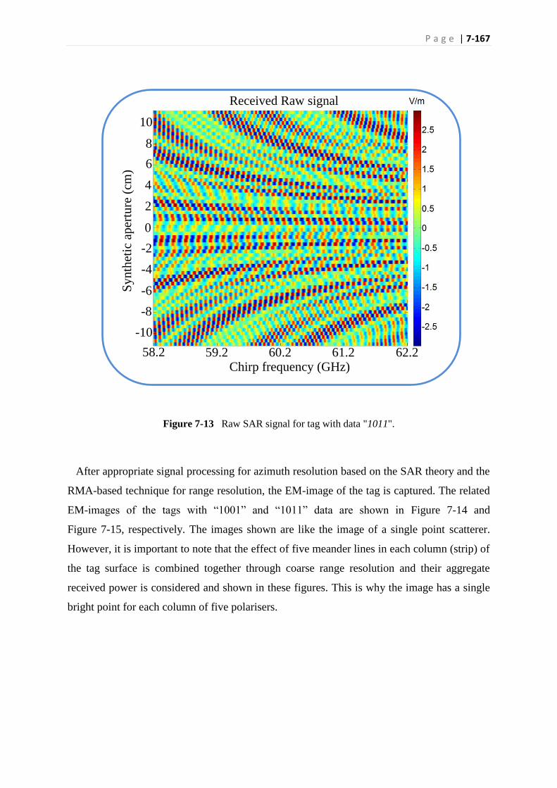
P a g e | 7-167
Figure 7-13 Raw SAR signal for tag with data "1011".
After appropriate signal processing for azimuth resolution based on the SAR theory and the
RMA-based technique for range resolution, the EM-image of the tag is captured. The related
EM-images of the tags with “1001” and “1011” data are shown in Figure 7-14 and
Figure 7-15, respectively. The images shown are like the image of a single point scatterer.
However, it is important to note that the effect of five meander lines in each column (strip) of
the tag surface is combined together through coarse range resolution and their aggregate
received power is considered and shown in these figures. This is why the image has a single
bright point for each column of five polarisers.
58.2 59.2 60.2 61.2 62.2Chirp frequency (GHz)
Sy
nth
etic
ap
ertu
re (
cm)
Received Raw signal
0
-2
-10
-8
4
10
6
8
2
-4
-6
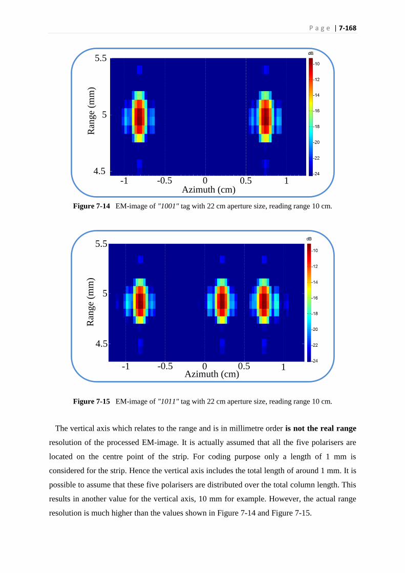
P a g e | 7-168
Figure 7-14 EM-image of "1001" tag with 22 cm aperture size, reading range 10 cm.
Figure 7-15 EM-image of "1011" tag with 22 cm aperture size, reading range 10 cm.
The vertical axis which relates to the range and is in millimetre order is not the real range
resolution of the processed EM-image. It is actually assumed that all the five polarisers are
located on the centre point of the strip. For coding purpose only a length of 1 mm is
considered for the strip. Hence the vertical axis includes the total length of around 1 mm. It is
possible to assume that these five polarisers are distributed over the total column length. This
results in another value for the vertical axis, 10 mm for example. However, the actual range
resolution is much higher than the values shown in Figure 7-14 and Figure 7-15.
5
5.5
4.50 0.5-0.5-1 1
Azimuth (cm)
Ran
ge
(mm
)
0 0.5-0.5-1 1
4.5
5
5.5
Ran
ge
(mm
)
Azimuth (cm)
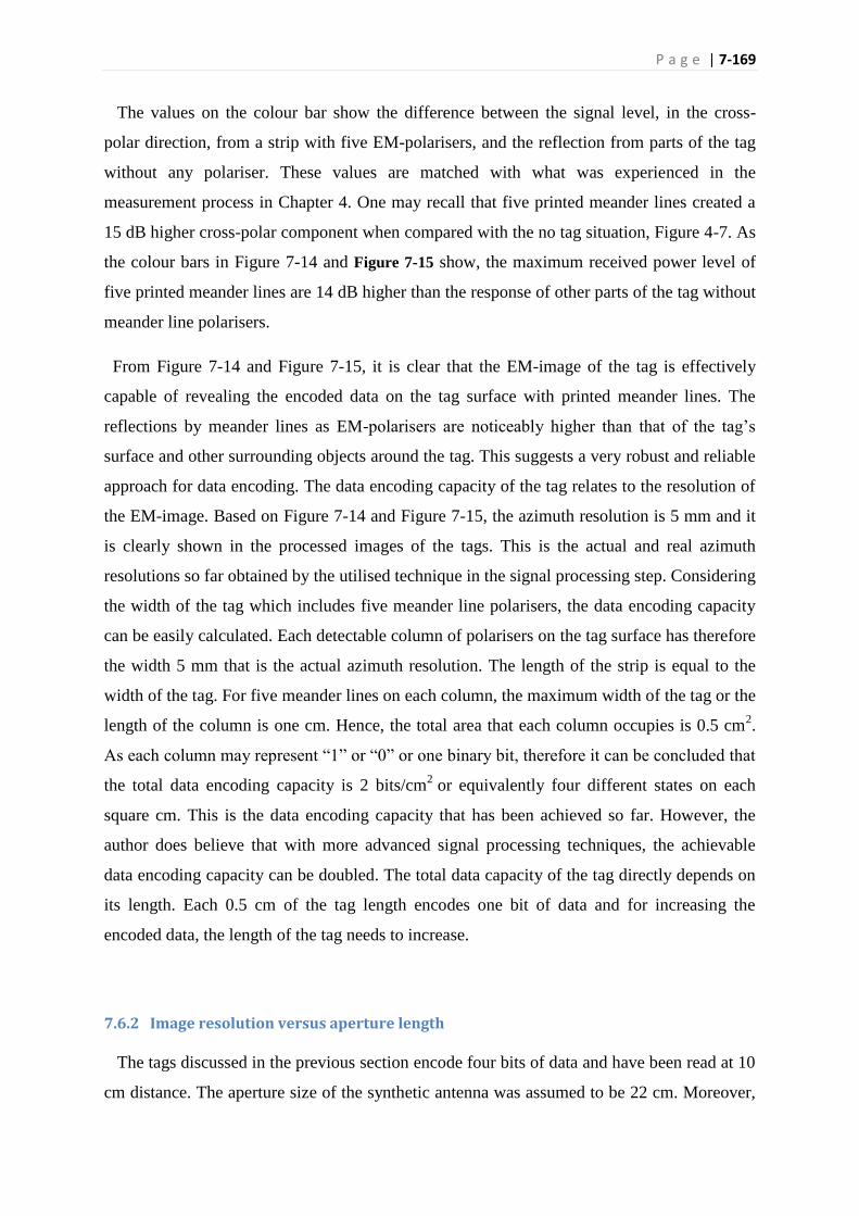
P a g e | 7-169
The values on the colour bar show the difference between the signal level, in the cross-
polar direction, from a strip with five EM-polarisers, and the reflection from parts of the tag
without any polariser. These values are matched with what was experienced in the
measurement process in Chapter 4. One may recall that five printed meander lines created a
15 dB higher cross-polar component when compared with the no tag situation, Figure 4-7. As
the colour bars in Figure 7-14 and Figure 7-15 show, the maximum received power level of
five printed meander lines are 14 dB higher than the response of other parts of the tag without
meander line polarisers.
From Figure 7-14 and Figure 7-15, it is clear that the EM-image of the tag is effectively
capable of revealing the encoded data on the tag surface with printed meander lines. The
reflections by meander lines as EM-polarisers are noticeably higher than that of the tag’s
surface and other surrounding objects around the tag. This suggests a very robust and reliable
approach for data encoding. The data encoding capacity of the tag relates to the resolution of
the EM-image. Based on Figure 7-14 and Figure 7-15, the azimuth resolution is 5 mm and it
is clearly shown in the processed images of the tags. This is the actual and real azimuth
resolutions so far obtained by the utilised technique in the signal processing step. Considering
the width of the tag which includes five meander line polarisers, the data encoding capacity
can be easily calculated. Each detectable column of polarisers on the tag surface has therefore
the width 5 mm that is the actual azimuth resolution. The length of the strip is equal to the
width of the tag. For five meander lines on each column, the maximum width of the tag or the
length of the column is one cm. Hence, the total area that each column occupies is 0.5 cm2.
As each column may represent “1” or “0” or one binary bit, therefore it can be concluded that
the total data encoding capacity is 2 bits/cm2
or equivalently four different states on each
square cm. This is the data encoding capacity that has been achieved so far. However, the
author does believe that with more advanced signal processing techniques, the achievable
data encoding capacity can be doubled. The total data capacity of the tag directly depends on
its length. Each 0.5 cm of the tag length encodes one bit of data and for increasing the
encoded data, the length of the tag needs to increase.
7.6.2 Image resolution versus aperture length
The tags discussed in the previous section encode four bits of data and have been read at 10
cm distance. The aperture size of the synthetic antenna was assumed to be 22 cm. Moreover,

P a g e | 7-170
the reader moved on a linear route around the tag. The graphs in Figure 7-8, however suggest
smaller aperture size for the 5 mm image resolution in the reading distance of 10 cm. Testing
this suggestion, aperture sizes less than 22 cm are considered. Two lengths of 12 and 17 cm
are assumed for the synthetic aperture length. The EM-images of the same tag as for
Figure 7-15, “1011”, are shown in Figure 7-16 and Figure 7-17 for the aperture lengths 12
and 17 cm, respectively.
As is clear from Figure 7-16, the provided image by 12 cm aperture size does not decodes
the tag’s data of “1011”. The effect of each column of polarisers has spread over the other
segments of the image that is not matched with the initial size of the tag. The image in
Figure 7-16 has almost five cm length while the initial tag is only two cm long. Hence, the
image resolution of 5 mm is no longer existed for the case of 12 cm aperture size.
Figure 7-16 EM-image of the tag "1011" with 12 cm aperture size.
Increasing the aperture size to 17 cm elevates the final image resolution. In this case, the
effects of three columns of polarisers are detectable on the tag’s image. However, the final
azimuth resolution is less than what is already shown in Figure 7-15. Again, the image of the
tag spreads to three cm while the initial tag is two cm. Moreover, the vertical position of the
column of polarisers in Figure 7-15 is very clear and matches the actual position of the
meander lines on the tag surface. While in Figure 7-17, the image shows inclined rows of
4.5
5
5.5
0 0.5-0.5-1 1-1.5 1.54.1
-2 2-2.5Azimuth (cm)
Ran
ge
(mm
)
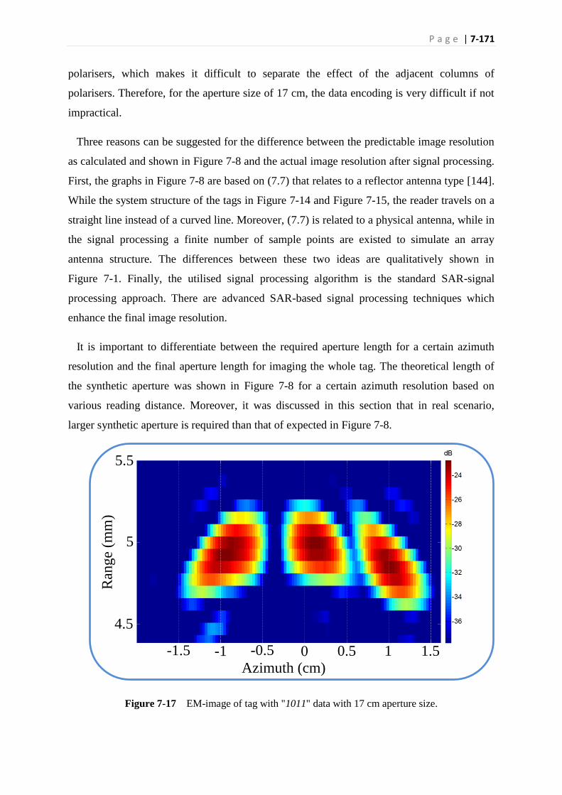
P a g e | 7-171
polarisers, which makes it difficult to separate the effect of the adjacent columns of
polarisers. Therefore, for the aperture size of 17 cm, the data encoding is very difficult if not
impractical.
Three reasons can be suggested for the difference between the predictable image resolution
as calculated and shown in Figure 7-8 and the actual image resolution after signal processing.
First, the graphs in Figure 7-8 are based on (7.7) that relates to a reflector antenna type [144].
While the system structure of the tags in Figure 7-14 and Figure 7-15, the reader travels on a
straight line instead of a curved line. Moreover, (7.7) is related to a physical antenna, while in
the signal processing a finite number of sample points are existed to simulate an array
antenna structure. The differences between these two ideas are qualitatively shown in
Figure 7-1. Finally, the utilised signal processing algorithm is the standard SAR-signal
processing approach. There are advanced SAR-based signal processing techniques which
enhance the final image resolution.
It is important to differentiate between the required aperture length for a certain azimuth
resolution and the final aperture length for imaging the whole tag. The theoretical length of
the synthetic aperture was shown in Figure 7-8 for a certain azimuth resolution based on
various reading distance. Moreover, it was discussed in this section that in real scenario,
larger synthetic aperture is required than that of expected in Figure 7-8.
Figure 7-17 EM-image of tag with "1011" data with 17 cm aperture size.
4.5
5
5.5
0 0.5-0.5-1 1-1.5 1.5
Azimuth (cm)
Ran
ge
(mm
)

P a g e | 7-172
It is crucial to emphasize that this length is the minimum length, known as fundamental
aperture length (Df) that is required to provide the expected resolution. However, for covering
the whole tag, the reader shall move more than this fundamental aperture length. This
operation is shown in Figure 7-18. The reader is required to move around the tag for Df length
to be able to provide a certain azimuth resolution. For example, 20 cm synthetic aperture is
required for 5 mm resolution as shown in Figure 7-14 and Figure 7-15. However, as the tag is
4 bits and has 2 cm length, hence the final synthetic aperture size would be 22 cm to cover
the whole tag for data decoding purpose. The results are shown in Table 7-1. As one may
notice the fundamental aperture length of less than 20 cm is not large enough for targeted 5
mm image resolution.
Table 7-1 Synthetic aperture size and image resolution
Minimum
final
Aperture
length (cm)
Fundamental
aperture
length (Df)
(cm)
Image
resolution
(mm)
Tag length
(cm)
Tag data
capacity
Reading
process
12 10 > 5 2 4 Not successful
17 15 > 5 2 4 Not successful
22 20 5 2 4 successful
24 20 5 4 8 successful
25.5 20 5 5.5 11 successful
28.5 20 5 8.5 17 successful
Figure 7-18 Final and fundamental aperture length.
Antenna azimuthradiation pattern
Tag
Reader antenna
Fundamental synthetic aperture (Df)
L
Final fundamental synthetic aperture (D)
L

P a g e | 7-173
Therefore, the length of 12 and 17 cm were not able to decode a tag with 4 bits data
encoding capacity and 2 cm tag length. If the fundamental aperture length 20 cm is
addressed, then based on the length of the tag, the final aperture length is determined. The
values of Table 7-1 are considered for the measurement of higher bits tag at the rest of this
chapter.
7.6.3 High data content tags
In Section 7.6.2, the concept of EM-imaging for data encoding purposes was presented and
its applicability is aproved. It was shown that a four bits tag can be read at 10 cm distance
through a moving reader and after post signal processing, the EM-image of the tag at a cross-
polar direction successfully reveals the encoded data on the tag surface.
In this section, the final data encoding capacity of the proposed approach is shown. It is
important to mention that similar to any other approaches in the chipless RFID system, the
final data encoding capacity of the tag directly depends on its physical size. Obviously, more
data can be encoded on a larger tag surface. Normally the credit card size of 55 × 85 mm2 is
considered as the maximum allowable size of a chipless RFID tag. The maximum data
encoding capacity of any proposed technique is considered based on this maximum allowable
physical size.
Multiple tag structures with different encoded data are considered to show the performance
of the proposed theory and its final data encoding capacity. The printed tag structure, its
received raw signal, and finally, its EM-image is shown in Figure 7-19 for a tag with eight
bits of data. As suggested, the tag length is four cm and its width almost one cm. The
expectation is to encode one binary code in each 5 mm of the tag length. The final image of
the tag clearly shows the position of each column of 5 polarisers on the tag surface. There is
no overlay between adjacent columns. The SAR aperture size is (20+4) cm. 20 cm is required
for 5 mm azimuth resolution and 4 cm shall be added due to the total length of tag.
Figure 7-19 shows the tag image based on 24 cm total aperture. This length is shown in the
raw signal graph of Figure 7-19.
Figure 7-20 and Figure 7-21 show two tags with 11 and 17 data bits, respectively, along
with their final EM-image. The raw signals are not shown for these two cases. Again the
aperture size for each case is approximately the initial aperture length 20 cm plus the length

P a g e | 7-174
of tag. As is clear from the related EM-images, the processed image successfully reveals the
presence or absence of polarisers on each column of the tag surface, hence data decoding is
performed successfully. These results confirm the validity of the proposed theory at its
maximum performance capability. As discussed before, the acquired cross-range resolution is
again 5 mm and the width of the tag is around 10 mm with five polarisers on each column.
Therefore, the detectable data encoding capacity of the printed tag is 2 bits/cm2. For a
chipless tag of 8.5 × 1 cm2, 17 bits can be encoded as shown in Figure 7-21. This tag is 5.5
times smaller than a credit card (8.5 × 5.5 cm2). Hence it can be concluded that in an area
equivalent to a credit card, 93 bits encoding capacity is feasible. This encoding capacity for a
chipless RFID system is very attractive. However, when other aspects of the proposed
technique have been recalled, the significant advantages of the proposed technique are very
attractive for industries. The acquired data encoding capacity is based on a fully printed tag
structure. The printed tag is fabricated on a paper substrate with the minimum conductive ink
usage. There are many structural anomalies on the printed tag. Irrespective of these printing
issues, it performs adequately for data encoding purposes. The robustness of the proposed tag
structure with respect to multipath and clutter interferences has been already shown through
measurements. The chipless tag is also applicable for tagging of metallic and high reflective
items. The tag provides a reasonable performance when bent around on the products’ surface.
Considering all of these aspects of the tag, specifically its data encoding capacity, it can be
concluded that a very successful and innovative approach has been proposed for the chipless
RFID systems.
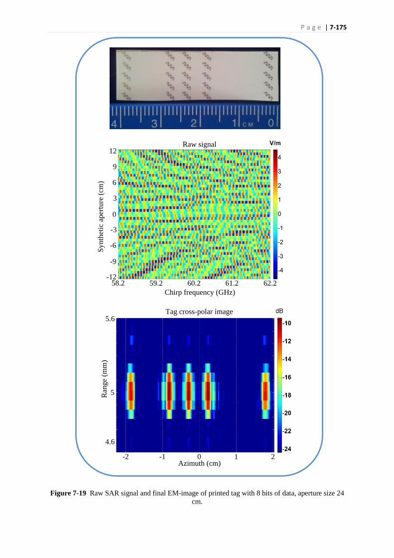
P a g e | 7-175
Figure 7-19 Raw SAR signal and final EM-image of printed tag with 8 bits of data, aperture size 24
cm.
58.2 59.2 60.2 61.2 62.2
Chirp frequency (GHz)
Sy
nth
etic
ap
ertu
re (
cm)
Raw signal
0
-3
-12
6
9
12
3
-6
-9
Tag cross-polar image
Azimuth (cm)
Ran
ge
(mm
)
5.6
4.6
5
0 1 2-1-2
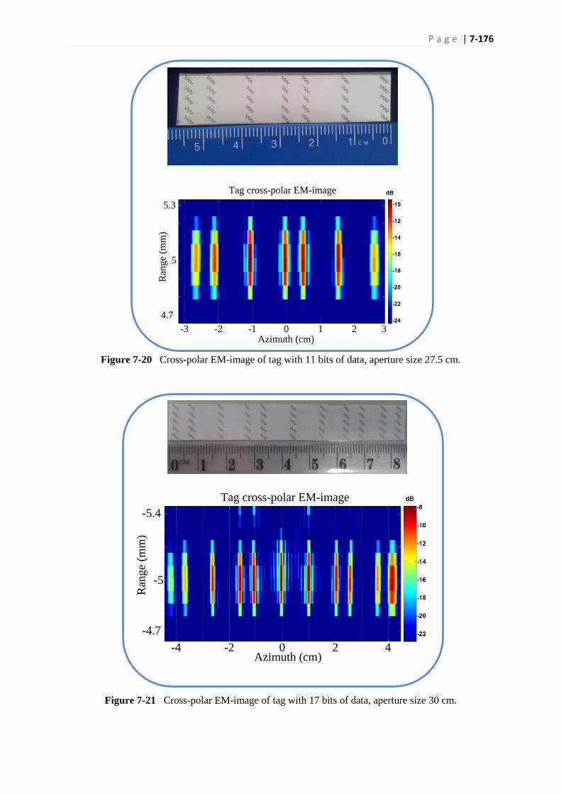
P a g e | 7-176
Figure 7-20 Cross-polar EM-image of tag with 11 bits of data, aperture size 27.5 cm.
Figure 7-21 Cross-polar EM-image of tag with 17 bits of data, aperture size 30 cm.
Azimuth (cm)0 1-1 2-3 -2
Ran
ge
(mm
)
5.3
4.7
5
Tag cross-polar EM-image
3
Ran
ge
(mm
)
-4.7
-5
-5.4
0 42-4 -2Azimuth (cm)
Tag cross-polar EM-image
P a g e | 7-177
7.7 Conclusion
The synthetic aperture radar theory has been briefly reviewed in this chapter. It was shown
that tag imaging requires the implementation of the synthetic aperture theory with regard to
some technical requirements. Then three modes of operation of the SAR theory along with
their attributes and limitations were discussed. Although the strip map mode is applicable for
the proposed application, the spotlight mode is able to provide better azimuth resolution due
to the increased length of the synthetic aperture size. Hence, the spotlight mode of operation
was proposed as the image resolution with the highest priority in the proposed application.
Then the image resolution in range and azimuth direction was associated with the system
parameters such as frequency of operation, available bandwidth, reading range, and synthetic
aperture size. Based on the features of the chipless tag, it was found that fine range resolution
is not achievable considering the limited available frequency band. Hence in the proposed
theory of EM-imaging, only azimuth resolution can be used for data decoding purposes.
Based on this, the final tag structure and data encoding algorithm were proposed. The
theoretical data encoding capacity of the system was also introduced and provides a very high
data encoding capacity. The required aperture size, reading distance and other parameters
were also included in the calculations and assumptions.
In the final stage of this chapter, the electromagnetic images of some sample tags with
different data encoding capacity have been shown. First simple tags with only four bits of
data were reviewed. Their final EM-image successfully decoded the tags’ data that revealed
the applicability of the proposed theory of imaging for chipless RFID application. The effect
of aperture size was also considered at this stage. It was found that the actual required
aperture size was almost compatible with what was expected through theoretical calculation.
The final achieved image resolution is 5 mm in azimuth direction based on the straight
trajectory of the reader, in the strip map mode. However, if the final curvature movement of
the reader is inserted in the signal processing process, in the spotlight mode, the better
azimuth resolution of 2 mm can easily be expected. Then based on the satisfactory results
gained from the 4 bits tags, larger tags with higher content capacity were considered. The
maximum length of the RFID tag, 8.5 cm, was utilised to encode 17 bits of data while the tag
width is only 1cm, 5.5 times narrower than a credit card size. This step revealed the ultimate
data encoding capacity of the proposed technique beyond 90 bits/credit card or 2 bits/cm2.
This suggested a very attractive content capacity for a chipless RFID system, based on results

P a g e | 7-178
that have come from a fully printable tag structure measured in a lab environment with high
multipath interference and clutter robustness, as discussed previously.
Considering the final result achieved through signal processing in this chapter, it can be
concluded that the EM-imaging is an applicable technique for chipless RFID system. This is
the first time that all details of EM-imaging chipless RFID system has been publicly
disclosed which may open a new area of research for the chipless RFID systems and other
applications. It was discussed earlier that other approaches normally rely on the frequency
domain and time domain responses of the tag. However, the proposed approach of cross-
polar EM-imaging suggests an alternative methodology for data encoding on the tag surface,
that is fully robust to printing inaccuracy and low Q factor of the printed circuit on the tag.
While EM-imaging can be considered as an independent technique for chipless RFID
systems, it may combined with other conventional approaches in chipless RFID systems for
enhancement of their capabilities. The few limitations of the proposed technique are
discussed in the next chapter along with some practical solutions for addressing them.

P a g e | 8-179
Chapter 8 MIMO-based array antenna for fast imaging
8.1 Introduction
EM-imaging as a data encoding approach for the chipless tag has been introduced earlier. It
is confirmed that EM-imaging is an effective approach to high data capacity chipless RFID
systems. The measurement results have revealed the salient attributes of the SAR imaging
technique regarding its: i) superior data encoding capacity, ii) robustness detection against
multipath and clutter interferences, and iii) reliable performance to printing inaccuracy.
However, there are two limitations associated with the proposed EM-imaging technique that
may deter its full potentials in mass deployment of the chipless RFID systems in the market.
The main issue which is associated with the proposed EM-imaging technique is the
requirement for relative movement of the reader and tag. This chapter considers this
limitation and proposes a fairly simple solution for accelerating the tag imaging process. The
second limitation that is the tag orientation sensitivity, is addressed in Chapter 9.
This chapter is organised as follow: i) requirement of the relative movement of the reader
and tag in the proposed EM-imaging technique is first introduced. ii) the phased array
antennas with agile beamforming capability are considered as a solution for reader movement
and its system complexity is discussed. iii) the new idea of MIMO-based array antenna is
presented. iv) a MIMO-based array antenna is designed for fast imaging of the tag and the
result of simulation is presented. Finally, v) the approach for optimization of the MIMO-
based system is introduced as the next phase of this research. The stream of discussion in this
Chapter is shown in Figure 8-1.
8.2 Reader physical movement
EM-imaging of the tag’s surface through SAR requires relative movement of the reader
antenna with respect to the tag. As the tag is normally fixed or its movement trajectory is not
predictable, hence a fixed tag and a moving reader antenna are assumed to be the most
practical system configuration. Therefore, a moving reader antenna on a defined trajectory
around the tag, is the general case of the proposed system configuration. As discussed in
Chapter 7, illumination of the tag and gathering its backscattered signal from different view
angles normally requires large number of individual transmit and receive scans, for example
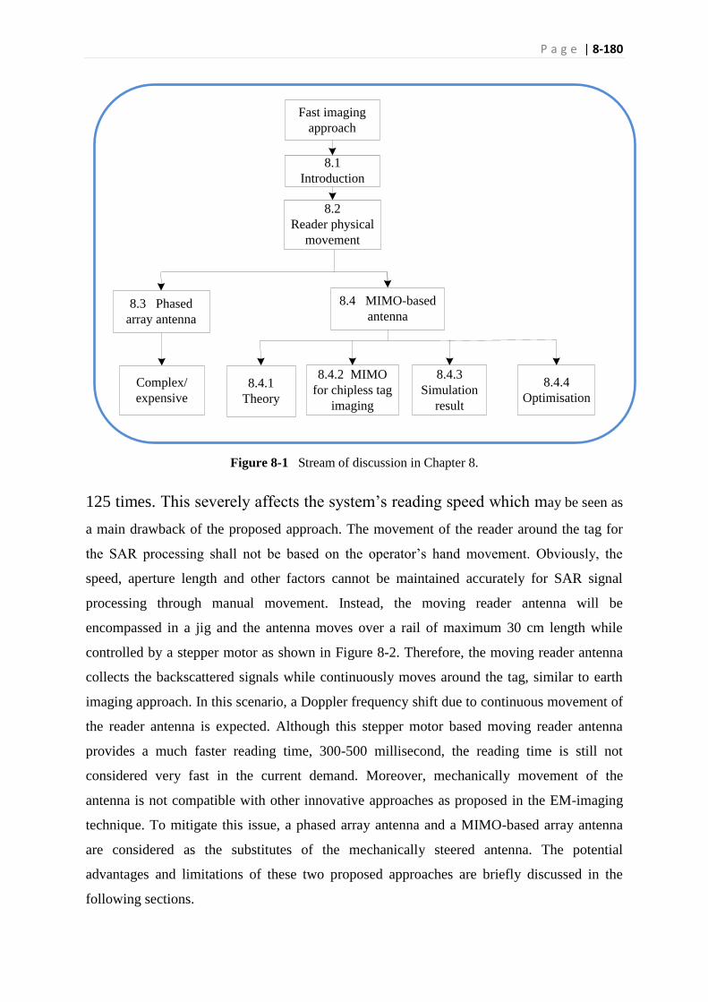
P a g e | 8-180
Figure 8-1 Stream of discussion in Chapter 8.
125 times. This severely affects the system’s reading speed which may be seen as
a main drawback of the proposed approach. The movement of the reader around the tag for
the SAR processing shall not be based on the operator’s hand movement. Obviously, the
speed, aperture length and other factors cannot be maintained accurately for SAR signal
processing through manual movement. Instead, the moving reader antenna will be
encompassed in a jig and the antenna moves over a rail of maximum 30 cm length while
controlled by a stepper motor as shown in Figure 8-2. Therefore, the moving reader antenna
collects the backscattered signals while continuously moves around the tag, similar to earth
imaging approach. In this scenario, a Doppler frequency shift due to continuous movement of
the reader antenna is expected. Although this stepper motor based moving reader antenna
provides a much faster reading time, 300-500 millisecond, the reading time is still not
considered very fast in the current demand. Moreover, mechanically movement of the
antenna is not compatible with other innovative approaches as proposed in the EM-imaging
technique. To mitigate this issue, a phased array antenna and a MIMO-based array antenna
are considered as the substitutes of the mechanically steered antenna. The potential
advantages and limitations of these two proposed approaches are briefly discussed in the
following sections.
8.2
Reader physical
movement
8.3 Phased
array antenna
Complex/
expensive
8.4.3
Simulation
result
8.4.4
Optimisation8.4.1
Theory
Fast imaging
approach
8.4 MIMO-based
antenna
8.1
Introduction
8.4.2 MIMO
for chipless tag
imaging

P a g e | 8-181
Figure 8-2 Handheld reader with mechanically moving antennas.
8.3 Conventional phased array antenna
Phased array antennas have emerged as the most advanced technology in the modern day
radar systems. It provides huge enhancement in performances that are of interests in radar
systems, modern wireless communications and many commercial applications. In a phased
array antenna, antenna elements are precisely controlled in relative excitation of phase and
amplitude to generate directional beams and nulls in desired direction [144].
Figure 8-3 shows the block diagram of a phased array antenna. As is shown in the figure,
the signal first arrives (or departs) to the right element. The second element of the array
receives the signal with Δt delay. The next element receives the signal with a delay of 2× Δt
and so on. If proper phase adjustment is utilized at the feeding point of each array element,
then the signal from a desired direction, θ for instance, could be constructively added to each
other. This simply means that the whole array performs as a unique antenna and effectively
receives signals from the direction θ.
Stepper motor
~
~
Display
Tx
Rx
< 30 cm
10-5
0 cm
Handheld
reader
Printed tag
P a g e | 8-182
Appropriate relative phase adjustments of the array elements in the time domain is known
as the time domain beamforming. This happens by creating precise time delays in the
received signals of each array element. Time domain beamforming provides an accurate
result for a wideband signal, however, the precision of the delays are restricted to the
capabilities of devices for precise time delay control.
It is also possible to use the fast Fourier transform (FFT) and transfer the required
adjustment of the array elements in the frequency domain instead of time domain through the
following equations:
( ) ( )
2 cos( )( ) ( ) ; .j t
F x t X j
fdF x t t X j e t
c
(8.1)
where x(t) is the receive (transmit) radar signal in time domain and X(jω) is its Fourier
transform, d is the inter-element distance f is the frequency of operation, Δt is the relative
time delay between each adjacent elements, ω is the equivalent frequency domain of the
signal and Δφ is the equivalent phase shift in each adjacent elements.
This means that through specific phase shift in the feeding route of each array element, the
array can steer on a specific direction. Solid state digital phase shifters and voltage variable
controlled attenuators are widely developed nowadays on which precise adjustment of each
antenna element is possible based on the required “weight vectors”. The frequency domain is
a more common technique in the phased array systems than the time delay approach as it can
provide much more accurate beamforming results.
Applying the phased array antenna theory to the proposed image-based chipless RFID
system, two difficulties shall be considered. First, in the phased array structure, phase shifters
or their equivalent time delay modules are needed. To precisely scan the tag surface in the
order of a few millimetres, the phase shifters’ granularity shall be very fine [163, 164].
Utilizing accurate phase shifters in the 60 GHz frequency band significantly increases the
system cost. Moreover, when the phased array antenna scans the tag, the beam shape
distorted with the view angle. This may not be a serious issue in many applications, however
in the proposed EM-imaging theory, the fixed shape of the radiation pattern is vital otherwise
the tag’s image is distorted [74].
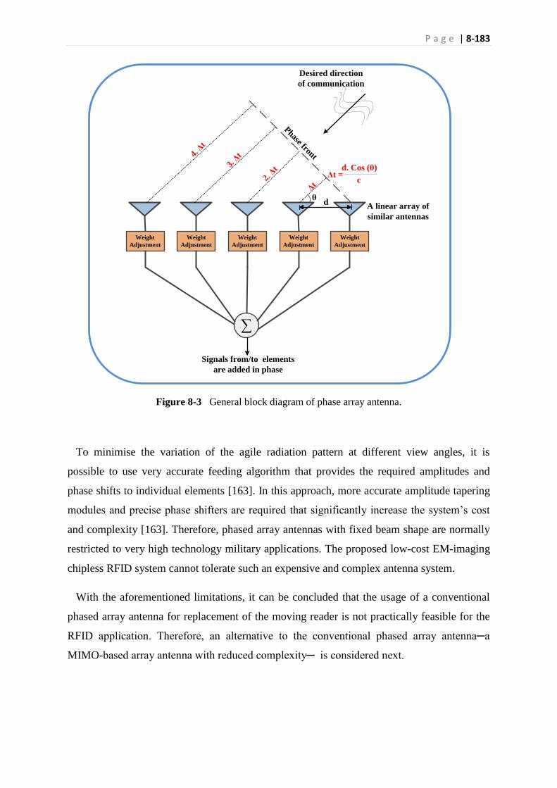
P a g e | 8-183
Figure 8-3 General block diagram of phase array antenna.
To minimise the variation of the agile radiation pattern at different view angles, it is
possible to use very accurate feeding algorithm that provides the required amplitudes and
phase shifts to individual elements [163]. In this approach, more accurate amplitude tapering
modules and precise phase shifters are required that significantly increase the system’s cost
and complexity [163]. Therefore, phased array antennas with fixed beam shape are normally
restricted to very high technology military applications. The proposed low-cost EM-imaging
chipless RFID system cannot tolerate such an expensive and complex antenna system.
With the aforementioned limitations, it can be concluded that the usage of a conventional
phased array antenna for replacement of the moving reader is not practically feasible for the
RFID application. Therefore, an alternative to the conventional phased array antenna─a
MIMO-based array antenna with reduced complexity─ is considered next.
Weight
Adjustment
Weight
Adjustment
Weight
Adjustment
Weight
Adjustment
Weight
Adjustment
∑
A linear array of
similar antennas
Phase front
Δt
dθ
Signals from/to elements
are added in phase
2. Δ
t3. Δ
t4. Δ
t
Δt = d. Cos (θ)
c
Desired direction
of communication
P a g e | 8-184
8.4 MIMO-based phased array antenna
Considering the potential advantages on providing flexibilities and freedom due to the
usage of multiple channels, the MIMO-based systems are of interests to researchers [165].
MIMO technique has recently provided noticeable simplifications on radar systems [166-168].
MIMO-SAR that employs multiple antennas to transmit orthogonal waveforms and multiple
antennas to receive radar echoes. MIMO-SAR is recently proposed in remote sensing concept
[169]. It is shown that the MIMO-SAR can be used to improve the remote sensing system
performance. One of the main advantages of the MIMO-SAR is the greatly increased degrees
of freedom by the concept of virtual antenna array [166]. In the conventional phased array
radars, the transmitted signals through array elements are inherently dependants and only
vary by some time delays or its equivalent phase shifts. However, in the MIMO-based system,
each antenna transmits a unique waveform that is orthogonal to the waveforms transmitted by
other antennas. This means that the return signals to each receive antenna element will carry
independent information about the target, hence increasing the system freedom and flexibility.
The phase difference caused by different transmitting antennas along with the phase
differences caused by different receiving antennas can form a new virtual antenna array
steering vector [166]. With optimally designed array elements’ positions, a very long array
steering vector with a small number of antennas can be created. This provides high flexibility
and reconfigurability in antenna configuration [166, 170].
The idea of the MIMO-based array antenna is applied on the chipless RFID system. It is
found that the new technique of MIMO-based array has huge potential for increasing the tag
imaging time on a fairly low cost and simple reader configuration. This idea is introduced and
developed further at the rest of this chapter for the chipless RFID imaging.
8.4.1 MIMO-based array theory
An 8-element MIMO-based antenna and its equivalent sparse arrays are shown in
Figure 8-4. It shows the relation between the MIMO system and the traditional array antenna.
In this simple example, four Tx and four Rx planar MIMO antennas are connected to each
other [171]. It is envisioned to show the transition between the MIMO theory and its
equivalent virtual array antenna without being deeply involved with the mathematical
calculations.
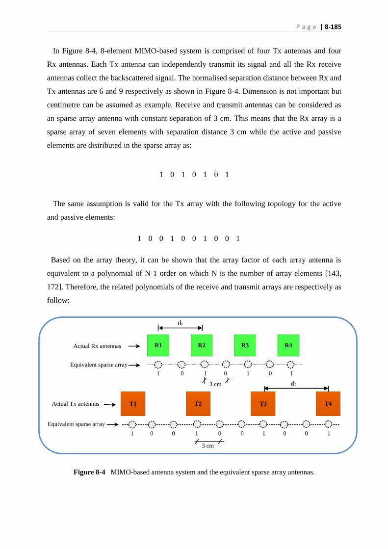
P a g e | 8-185
In Figure 8-4, 8-element MIMO-based system is comprised of four Tx antennas and four
Rx antennas. Each Tx antenna can independently transmit its signal and all the Rx receive
antennas collect the backscattered signal. The normalised separation distance between Rx and
Tx antennas are 6 and 9 respectively as shown in Figure 8-4. Dimension is not important but
centimetre can be assumed as example. Receive and transmit antennas can be considered as
an sparse array antenna with constant separation of 3 cm. This means that the Rx array is a
sparse array of seven elements with separation distance 3 cm while the active and passive
elements are distributed in the sparse array as:
1 0 1 0 1 0 1
The same assumption is valid for the Tx array with the following topology for the active
and passive elements:
1 0 0 1 0 0 1 0 0 1
Based on the array theory, it can be shown that the array factor of each array antenna is
equivalent to a polynomial of N-1 order on which N is the number of array elements [143,
172]. Therefore, the related polynomials of the receive and transmit arrays are respectively as
follow:
Figure 8-4 MIMO-based antenna system and the equivalent sparse array antennas.
dt
dr
R1 R2 R3 R4
T1 T2 T3 T4
1 1 1 10 0 0
1 1 1 10 0 00 0 0
Actual Rx antennas
Equivalent sparse array
Actual Tx antennas
Equivalent sparse array
3 cm
3 cm

P a g e | 8-186
6 5 4 3 2
r
9 8 7 6 5 4 3 2
t
6 4 2
9 6 3
P 1 . 0. 1. 0. 1. 0. 1 ;for Rx array
P 1 . 0. 0. 1. 0. 0. 1. 0. 0. 1 ;for Tx array
1
1
z z z z z z
z z z z z z z z z
z z z
z z z
(8.2)
It can be mathematically proven that the two sets of Tx and Rx antennas on MIMO-based
configuration is equivalent to a virtual array antenna. This means that instead of analysing the
MIMO-based antenna, one may consider the equivalent virtual array and almost expect the
same radiation characteristics as the MIMO-based antenna. The details of expressions for
relation between the MIMO-based system and the virtual array are not discussed here. It has
been shown that the convolution of the Tx and Rx arrays defines their equivalent virtual array
antennas and subsequently specifies the position of the active elements in the virtual array
configuration [166, 171]. Therefore, two sets of the Tx and Rx antennas that have been
considered as sparse arrays are mathematically linked to their virtual array antenna. Based on
this assumption, the convolution of the Tx and Rx antennas in the time domain is equivalent
to multiplication in the frequency domain. Hence, one may simply find the equivalent virtual
array’s polynomial through the following relation [166]:
15 13 12 11 10 9 8 7 6 5 4 3 2
v r tP P . P 2 2 1z z z z z z z z z z z z z (8.3)
where Pv is the polynomial of the virtual array. This polynomial which is in order of 15
relates to a 16-element linear array with the following active/passive topology:
1 0 1 1 1 1 1 1 1 1 1 1 1 1 0 1
In the above configuration, “0” means that position has no antenna and “1” represents an
active antenna. The red positions with “1” also show duplicate element position. With this
procedure, the MIMO-based structure of 4+4 physical elements is related to a virtual array of
4×4 elements. This idea is shown in Figure 8-5 which the physical MIMO based system and
its equivalent virtual array antenna are presented simultaneously.
To have a more physical sense of evolution from MIMO-based system to the array antenna
concept, one can track the signal route when it is transmitted by a specific transmit antenna
(Ti) and received by all receive antennas. Let consider dr and dt as the separation distance
between the Rx and TX antennas respectively. The relative position of each Tx antenna to the
centre point of the transmit array antenna is denoted by dtn and the relative position of each Rx
antenna to the centre point of receive array is shown by drm, where m, n = [1, 4].

P a g e | 8-187
Figure 8-5 MIMO-based antenna and its equivalent virtual array antenna.
When one of the transmit antenna is active then the received signals to all receive antennas
can be weighted by:
0
2( )( ).cos( )
, 0( )rmtn
fj d d
cm nw e
(8.4)
This clearly shows that the relative positions of each set of transmit and receive antenna and
the relative phase shift in its equivalent virtual array. To establish a unique phase centre for
all communication links between the transmit and receive antennas, one can shift the position
of transmitters to a fixed point, the centre of transmit array for instance, and then find the
phase shift occurring in the all receive array elements. This is shown for the two cases of T1
and T2 in Figure 8-6. While T1 antenna is dt1 shifted to the right, all its related Rx antennas are
equivalently shifted to the left side for the same amount. The same happens for case T2.
However, the amount of movement is now dt2. If the shifted Rx antennas for these two cases
are mapped to each other, they fill the gaps among physical elements. This is shown in
Figure 8-6 by the dashed arrows and circles among active antennas. If the same procedure
continues for T3 and T4, then the virtual array element is completed and would be similar to
the declared virtual array polynomial and the position of the antenna in the virtual array as:
1 0 1 1 1 1 1 1 1 1 1 1 1 1 0 1
R1 R2 R3 R4
T1 T2 T3 T4
dt
dr
dtn
drm
Actual Rx antennas
Equivalent virtual arrays
Actual Tx antennas

P a g e | 8-188
Figure 8-6 Relative phase shift between one particular Tx antenna and all Rx antennas.
8.4.2 MIMO-based array for chipless RFID imaging
To design the MIMO-based phased array antenna for the proposed chipless RFID system,
the process described in [81] is followed. In the proposed configuration, every two Rx
antennas are linked with five Tx antennas. Then the structure is cascaded to provide the larger
required equivalent array antenna. The details of this proposed approach is discussed here and
the simulation result is based on this configuration. However, the author believes that the
proposed configuration of two Rx and five Tx antennas are not the best and optimum solution
for large arrays. This issue will be discussed at the end of this chapter.
In Figure 8-7, the structure of the MIMO-based antenna is presented. It is important to find
the separation distance between the Rx and Tx antennas on their array configuration. The
angles θ1 and θ2 can be linked to other parameters as follow:
0 01 2
0 0
2 2;
r r r
y ytan tan
X X X
(8.5)
where the parameters of (8.5) are defined in Figure 8-7. To find the position of the points a
and b, one can write the following expressions:
0 0 00 0 0
1 0
0 00 0 0 0
2 0
( ) 1
2 2
1( ) ( )
2 2
ra r r r
b r r r r r r r r
y y Xx X X X
tan y
y yy X X X X X X X X
tan y
(8.6)
R1 R2 R3 R4
T1
dt1
T1
R1
T1
R2
T1
R3
T1
R4
dt1
R1 R2 R3 R4
T2
dt2
T2
R1
T2
R2
T2
R3
T2
R4
dt2

P a g e | 8-189
Figure 8-7 MIMO-based antenna and its equivalent virtual array.
Therefore, the separation distance of Rx antennas can be easily linked to the separation
point of the virtual array elements, ΔXv, through:
1
2b a v rx x X X (8.7)
If the same approach is followed for θ3 and the distance between points b and c is found,
one can easily reach to the following relation:
0 2 4t r vX X X (8.8)
We have already shown in Chapter 7 that the reader antenna has to illuminate the tag in the
SAR technique every 2 mm. Therefore, the inner-space of virtual array element shall be 2
mm and equivalently, the physical Rx antennas have to be 4 mm and Tx antennas 8 mm apart
from each other.
The total number of sampling points also governs the total number of required physical
antennas. We have already discussed that “m+n” elements in Rx and Tx configuration may
provide a virtual array of “m×n” elements. It is important to mention this is a theoretical
Xro
Xto
ΔXr
ΔXv
θ1θ2
a b c
Actual Rx antennas
Actual Tx antennas
Virtual array elements
X
Y
yo
yo
θ3

P a g e | 8-190
criterion and shows the minimum number of required actual Tx and Rx antennas. For
example, 8 and 13 physical antennas are utilized in [81] for only 44 virtual array elements.
Based on the above mentioned theoretical relation, less number of antennas is expected for 44
elements virtual array. For the case of RFID application, it was shown earlier that the reader
shall stop in around 125 individual points and illuminates the tag and capture the
backscattered signal. Thus, the number of demanded virtual array elements is 125 points. It is
possible to have slightly higher or even less number of array elements. Therefore, 125 points
can be seen as a rough estimate. The proposed MIMO-based system topology for the Rx
antenna in [81] includes two active antennas and then four passive elements in the sparse
array configuration, for the 11000011 array polynomial. The Tx antennas having one active
and one passive element scheme, 101010 for instance. Based on this assumption, the antenna
distribution scheme is as follow:
For Tx array antenna: 11000011000011000011
For Rx array antenna: 1010101010101010101010101
Based on the antenna distribution in Tx and Rx arrays, the following polynomials can be
related to the Rx and Tx antennas respectively for the 44 elements requirements:
19 18 13 12 7 6
24 22 20 4 2
1
... 1
r
t
P Z Z Z Z Z Z Z
P Z Z Z Z Z
(8.9)
Obviously the convolution of the above polynomials results in a virtual array of degree 43.
Similarly, for the case of 125 array elements, one may suggest the following polynomial for
the Rx array antennas. This array includes 24 active antennas.
67 66 61 60 55 54 49 48 43 42 37
36 31 30 25 24 19 18 13 12 7 6 1
r z z z z z z z z z z z
z z z z z z z z z z z z
P
(8.10)
Based on the above assumption for the Rx configuration, the related Tx antennas can be
defined through the following polynomials with 31 physical Tx antennas:

P a g e | 8-191
30
60 58 4 2 2
0
... 1 k
t
k
P Z Z Z Z Z
(8.11)
One may examine that the convolution of (8.10) and (8.11) which results in a polynomials
of degree 127 which includes all the required elements.
127
0
. i
total i
i
P a Z
(8.12)
In (8.12), coefficients ai may be different than “1”. In this case, it is not required to
consider all relevant combinations between an individual Tx and Rx antennas. Therefore,
through (31+24) physical antenna, it is possible to implement a virtual array with 127
elements. Through this configuration, the total number of array elements drops from 127×2 =
254 to only 31+24 = 55 elements. Moreover, the reading time in the proposed technique of
EM-imaging would significantly increase while no complex system structure is utilised.
The summary of the MIMO-based system can be compared with a physical array and the
conventional SAR technique as mentioned in Table 8-1. The conventional SAR technique has
the minimum system complexity due to the usage of only one antenna. However, it provides
a very slow imaging speed in conventional approach or slow imaging speed if a stepper
motor is utilised. It is possible to develop an array antenna for fast imaging process while it
requires huge number of elements which results in significant system cost. Instead, one may
use the MIMO-based system with much lower number of elements and the requirement for a
switching network.
Table 8-1 The MIMO-based advantages
Number of elements System complexity Imaging time
MIMO-based
antenna
M+N(min) Switching network Fast
Array antenna M×N Phase shifter/amplitude
tapering
Fast
Conventional
SAR
1 Physical antenna movement Very slow/Slow(stepper
motor)

P a g e | 8-192
8.4.3 Simulation result
Figure 8-8 shows the proposed structure of the MIMO-based system. 24 Rx antennas with 4
mm separation distance are linked with 31 Tx antennas with separation distance 8 mm. Hence,
the total aperture size is less than 25 cm (31 × 0.8 = 24.8 cm) that is completely matched with
the aperture sizes introduced in Chapter 7. The virtual array antenna with 127 elements is
located between the Rx and Tx antennas. No phase shifter or amplitude tapering network is
required. Only a switching network is utilized to connect one Tx and one Rx antennas at a
time.
To test the validity of the proposed technique of a MIMO-based reader, a 6-bits tag is
selected as example. The tag’s image is simulated through MIMO-based reader system and
then compared with the image through normal SAR technique. The result of signal
processing is shown in Figure 8-9. In the SAR technique which includes 125 individual send
and receive process, the EM-image is adequately shows the encoded data. If the same tag is
processed through a MIMO-based system which utilises 55 physical antennas, then the image
is depicted in Figure 8-9(c). The EM-image seems to be somehow noisier than that for the
conventional SAR. Moreover, the imaged column of meander lines shows a minor inclined
nature so slightly degrades the azimuth resolution. However, much faster imaging time of
MIMO-based system, in few milliseconds, compensates the noisier tag’s image. Moreover, it
is possible to use higher number of physical antennas on MIMO-based system and improve
the image quality. Alternatively, by optimisation of the antennas distribution on the MIMO-
basis system one may expect a higher quality of the imaged tag. The optimisation process of
the antennas distribution in the MIMO-based system is introduced in next section.
It should be noted that the usage of 24 Rx and 31 Tx antennas is based on the suggested
topology of 2 Rx- 5 Tx antennas [81] and then cascading them for the required large aperture.
This scenario is also based on linear sparse array theory assumption. Obviously, the number
of utilised antennas is significant and may put restriction on the practicality of the proposed
MIMO-based approach. This issue is discussed in next section. Moreover, the 6 bits tag was
also used to show the difference between normal SAR approach and MIMO-based technique.
The MIMO-based technique is capable of encoding 17 bits tag that is shown before in
Chapter-7.

P a g e | 8-193
Figure 8-8 MIMO-based antenna for EM-image based chipless RFID system.
8.4.4 System optimisation of MIMO-based antenna
As discussed earlier, (24+31) separate antennas are utilised for the implementation of 127
virtual array antenna. The number of required Tx and Rx antennas are derived through the
procedure introduced in [81]. However, the expectation is to have a virtual array of 127
elements with lower number of physical Tx and Rx antennas. This simply means the
proposed topology in [81] is not optimum and it is possible to reduce the number of actual
antennas and still expect the same virtual array. To optimise the MIMO-based system for the
minimum number of physical antennas, two approaches can be considered, analytical
approach and numerical optimisation approach. First, it is suggested to follow the analytical
approach and try to find the optimum number of antennas. The following criteria shall be
considered in optimisation process:
2 3
1 2
. 1 ... :The targeted polynomial
deg( ) deg( ) ;
( ) ;
( )
( )
n
r t
r t
r
t
P P Z Z Z Z
P m P n m
NoE P k Number of Rx element
NoE P t Number of Tx element
kc c
t
Min k t
(8.13)
In the above set of expressions, the product of Pr × Pt shall produce a complete polynomial
of order “n”. The number of active elements in the Rx and Tx series is shown by “k” and “t”,
H-pol
“24”fixedRXHorizontalantennas
Chipless Tag
V-pol
Virtualarraywith“127”elements
“31”fixedTXverticalantennas
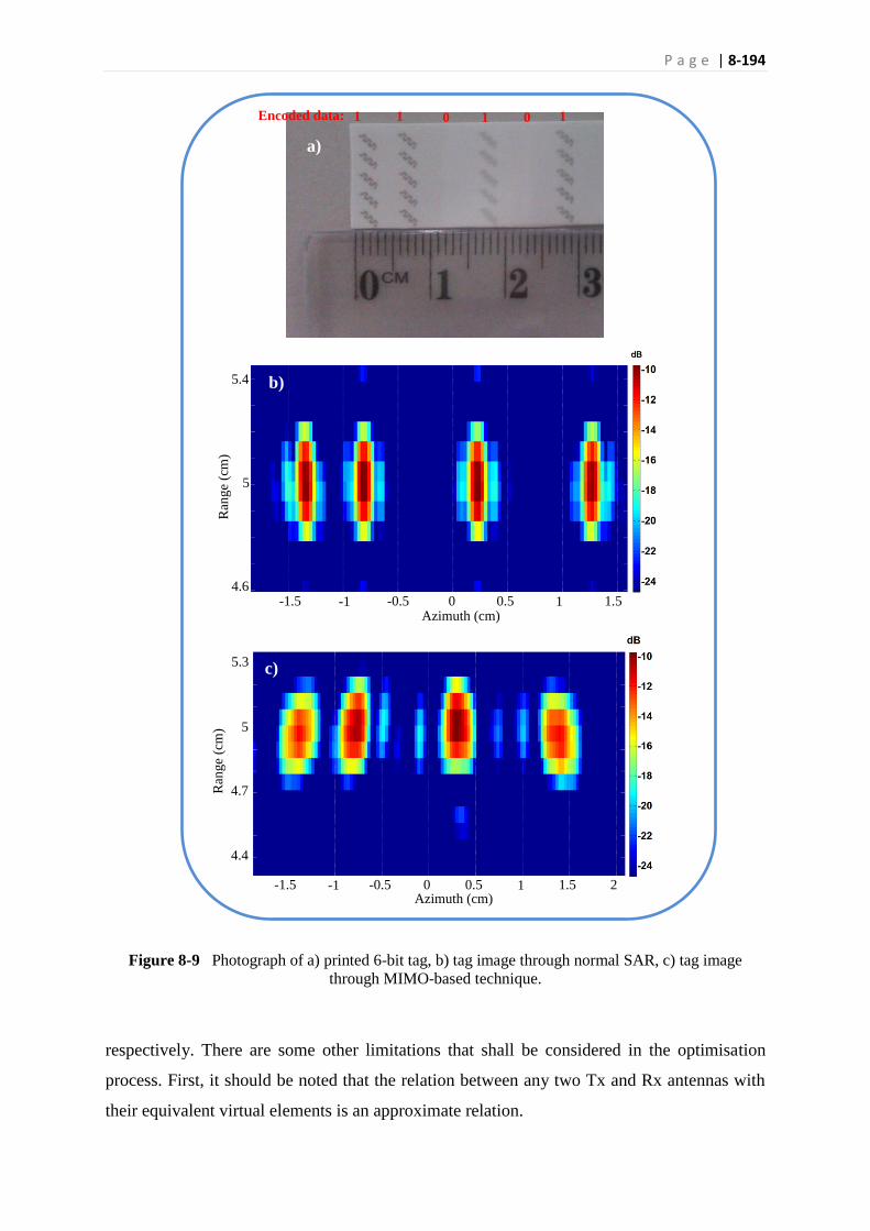
P a g e | 8-194
Figure 8-9 Photograph of a) printed 6-bit tag, b) tag image through normal SAR, c) tag image
through MIMO-based technique.
respectively. There are some other limitations that shall be considered in the optimisation
process. First, it should be noted that the relation between any two Tx and Rx antennas with
their equivalent virtual elements is an approximate relation.
11 1 10 0Encoded data:
Azimuth (cm)0 0.5-0.5-1 1-1.5 1.5
Ran
ge
(cm
)
2
5.3
5
4.7
4.4
Azimuth (cm)0 0.5-0.5-1 1-1.5 1.5
4.6
Ran
ge
(cm
)
5.4
5
a)
b)
c)

P a g e | 8-195
This relation is more accurate if the distance between the Tx and Rx antennas is negligible
with respect to the distance of the target in front of the antennas. This implies an additional
limitation in the above sets of formula in (8.13). Every Rx antenna shall be connected to its
neighbour Tx elements and not to the Tx antennas that are physically located far from the
intended Rx antenna. Otherwise, the results of analytical optimisation may be mathematically
accurate but results in an impractical system configuration. Second, the goal is to minimise
the k+t while it is also desirable to have the minimum physical space occupied by the
MIMO-based system. The other parameters of the system shall also be considered in the
above sets of formula. The author has started solve this mathematical problem through
analytical approaches and shall be introduced in future publications.
The second approach is the global optimisation process. If the analytical approach is not
able to find the best configuration of the Tx and Rx antennas for the minimum number of
physical antennas, then the global optimisation theories definitely help. In this case, the
uniform distribution of the Rx and Tx antennas on their sets may not be met. The global
optimisation process considers all available cases, which may exceed billions of possible
cases, and then try to find the best (optimum) configuration. The genetic algorithm would be
very suitable for this case as no real time solution is required [163, 173].
These two suggested approaches can be seen as the future direction of this research. There
are a very few published works on MIMO-based phase array antennas. In most of them, when
a large array structure is considered, the number and orientation set up of the Tx and Rx
antennas do not follow any regular/classical approach [167-169]. In all of the cases, the
utilised number of physical antennas is more than what expected through theoretical
limitations. The suggestion is that not enough investigation has been carried out on this issue
and the author believes that it is a very new and useful field of research. Any analytical and
or numerical approach for minimising the number of utilised antennas for the MIMO-based
phase array antenna significantly impacts on the current research and minimises the
fabrication cost and system complexity.
P a g e | 8-196
8.5 Conclusion
The requirement for relative movement of the reader and tag has been considered as the
main drawback of the proposed theory of EM-imaging for the chipless RFID systems. It was
discussed that although mechanical movement of the reader is practically possible, it may not
result in a time efficient process for tag imaging.
The possible solution of the phase array antenna was considered to provide a fast approach
for tag imaging. Considering the requirement of the image-based chipless RFID system to a
fixed radiation pattern in different scanning angle, it was addressed that the phase array
antenna requires a complicated feeding algorithm and very accurate phase shifters at 60 GHz.
This significantly increases the system cost that will not be accepted by industry. Hence, the
conventional phase array antennas found to be impractical for the proposed EM-imaging
chipless RFID system.
The new idea of MIMO-based array antenna was introduced. The theoretical basis of the
MIMO-based array antenna has been briefly explained. The relation between the MIMO-
based antenna and their equivalent virtual array was mathematically shown. Then based on
the available techniques in the MIMO-based array antenna, a system was designed for fast
imaging of a chipless RFID tag. The proposed MIMO-based system utilised 55 physical
antennas that was equivalent to a virtual array with 254 elements. This system was utilised
for chipless RFID tag imaging. Although the tag image through new MIMO-based reader
antenna showed minor degradation when compared with the result of normal SAR-based
system, the system performance was quite acceptable considering its much faster imaging
process.
Two approaches of analytical and global optimisations were proposed to optimise the
number of real antennas on the MIMO-based system for system cost and complexity
reduction. These two approaches are under investigation by the author and his colleagues and
shall be seen as an ongoing activity.
P a g e | 9-197
Chapter 9 Conclusion and future works
9.1 Review of the research
The main goal of this research was to introduce a new approach for data encoding on a
chipless RFID tag structure considering all practical limitations for the commercial phase of
the chipless RFID tags. This research was motivated by investigating the noticeable number
of previous works on chipless RFID systems with almost no real product on the market. First,
a comprehensive literature review on available techniques was accomplished to explore the
real challenges of the chipless RFID tags for the market acceptance. It was found that
regardless of many successful laboratory results, most of the proposed approaches were faced
significant challenges when their prototypes were tested based on the real market expectation.
Low quality materials used in a commercial tag structure along with fabrication inaccuracy
happened during inexpensive tag production process substantially reduce the performance of
the chipless tag in various techniques. It appeared that the researchers didn’t consider the
final commercial tag requirements in their investigations. This issue motivated the author to
suggest an approach which includes these practical limitations of the chipless RFID tags.
Inspired by the Earth imaging application, the idea of EM-imaging was initiated as a
possible solution for data encoding on a chipless RFID tag. This idea was completely
different than other techniques suggested so far for the chipless RFID tag. In all of other
conventional approaches, the tag surface is illuminated once by the reader, while in the
proposed approach of EM-imaging the tag surface shall be sequentially scanned in few
millimetres. Therefore, two questions arised. First, how to scan the tag surface with few
millimetre precision and second how to encode data in a very small area. It was found that the
ISM band 60 GHz has the potential providing such a precise tag scanning. Moreover, the
SAR technique found to be mandatory due to some technical limitations. The strip line and
meander line as EM-polarisers were also found to be suitable for data encoding considering
their miniaturised size due to the mm-wave band.
The idea of polariser-based tag has been investigated through extensive measurement
process. A printed tag was inspected regarding its performance on severe multipath and
clutter interferences. Moreover, the tag was used on highly reflective items like liquid
containers and metallic objects. The bent tag response was also investigated. The effect of
barriers was considered to explore the potential of the proposed tag for secure item

P a g e | 9-198
identification. The result of all those measurements disclosed the salient attributes of the
proposed tag. While many of the earlier proposed chipless RFID tags had difficulties in the
aforementioned scenarios, the satisfactory results of the proposed cross-polar based tag
suggested it as a suitable candidate for the real industrial applications.
In the next step, the printed tag was considered with appropriate SAR-based signal
processing algorithm for its EM-image. The tag was shaped based on a reasonable frequency
band for a course range resolution and through a practical synthetic aperture size for a fine
azimuth resolution of 5 mm. This provided the data encoding capacity of 2 bits/cm2 that
would be a revolutionary data encoding capacity for a printed tag structure. Multiple tags
with different data capacity have been investigated and their final EM-image successfully
decoded the tags’ contents. This proved the applicability of the EM-imaging technique
through proposed approach for data encoding purpose in a printable chipless RFID tag. The
utilised data encoding algorithm scenario effectively revealed information of a 17-bits tag
while the tag was 5.5 times smaller than a credit card. The potential advantages of the EM-
imaging technique would be very attractive for the identification industries as it suggests a
low cost identifications means with high data encoding capacity.
Finally, addressing the slow reading time of the proposed technique, the idea of MIMO-
based system was suggested for a fast EM-imaging. This idea showed satisfactory result
while it is required to continue the research for better performance and minimum number of
antennas.
The research and scholarship have been supported by the ARC Discovery Project Grant:
DP110105606: Electronically Controlled Phased Array Antenna for Universal UHF RFID
Applications. This research started on July 2011 and finished in February 2015.
9.2 Addressing the research objective
The new approach of mm-wave image-based chipless RFID system has provided a practical
solution for a low cost, fully printable tag with high content capacity in a reasonable tag size.
The proposed technique successfully showed its potential advantages for a chipless and
printable tag in the industrial environments with high multipath interferences. The proved
data encoding capacity was also much higher than that suggested for a printable chipless tag
to date.

P a g e | 9-199
The outcomes of the research which fulfils the research objectives are as: 1) proposing a
new idea in chipless RFID systems completely different than other conventional techniques,
2) introducing the strip line and meander line as effective EM-polarisers, 3) a cross-polar
working basis with many advantageous potentials for industrial environments, 4) new on/off
data encoding algorithm based on the performance of the printed tag structure, 5) tailoring the
SAR signal processing algorithm based on the requirements of the chipless RFID system, 6)
proposing the new approach of MIMO-based array antenna to tag fast imaging process.
The salient attributes of the proposed technique suggest it as a reliable new approach for
putting the chipless RFID system on track especially for main stream applications with
billions of yearly tag requirements. The stream of information on this dissertation can be
summarised as follow:
Chapter 1 outlines the overall work on mm-wave image-based chipless RFID system. First,
a brief overview of the industries with identification and tracking requirements was provided
to readers. These industries were categorized into various classes based on their tag
requirements. It was found that secure identification, anti-theft capability, cheap
identification solution, tagging of highly reflective products, high data capacity, tracking
along identification, identification through long reading range, and many more are examples
of important factors for industries. Irrespective of different priorities in product identification,
there are two main factors which matter in all applications: the data encoding capacity and
the system cost. For applications with millions of items for tagging, high data capacity of the
identification system is a must. However, for applications with a limited number of objects,
high data encoding capacity may be utilised for secure and higher reading reliability by
sacrificing some of the available data bits. Moreover, cost reduction is the main initiative for
the usage of the identification systems in industry. Obviously, the cost of the identification
system and its tagging price must be low and competitive enough to initiate the request for
the system. Barcode system as a well-stablished identification technique has been then
reviewed regarding its ultimate potentials for addressing the current demands of industries. It
was shown that the limitations of the barcodes on providing enough content capacity and also
their high labour cost are not compatible with the needs of industries in the modern
international trading market. The new idea of EM-imaging for data encoding purposes was
suggested and introduced briefly. The salient potentials of this new technique were disclosed,
which suggested a revolutionary enhancement of the system performance based on a fully
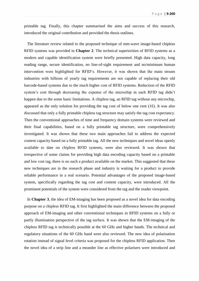
P a g e | 9-200
printable tag. Finally, this chapter summarised the aims and success of this research,
introduced the original contribution and provided the thesis outlines.
The literature review related to the proposed technique of mm-wave image-based chipless
RFID systems was provided in Chapter 2. The technical superiorities of RFID systems as a
modern and capable identification system were briefly presented. High data capacity, long
reading range, secure identification, no line-of-sight requirement and no/minimum human
intervention were highlighted for RFID’s. However, it was shown that the main stream
industries with billions of yearly tag requirements are not capable of replacing their old
barcode-based systems due to the much higher cost of RFID systems. Reduction of the RFID
system’s cost through decreasing the expense of the microchip in each RFID tag didn’t
happen due to the some basic limitations. A chipless tag, an RFID tag without any microchip,
appeared as the only solution for providing the tag cost of below one cent (1¢). It was also
discussed that only a fully printable chipless tag structure may satisfy the tag cost expectancy.
Then the conventional approaches of time and frequency domain systems were reviewed and
their final capabilities, based on a fully printable tag structure, were comprehensively
investigated. It was shown that these two main approaches fail to address the expected
content capacity based on a fully printable tag. All the new techniques and novel ideas openly
available to date on chipless RFID systems, were also reviewed. It was shown that
irrespective of some claims for providing high data encoding capacity based on a printable
and low cost tag, there is no such a product available on the market. This suggested that these
new techniques are in the research phase and industry is waiting for a product to provide
reliable performance in a real scenario. Potential advantages of the proposed image-based
system, specifically regarding the tag cost and content capacity, were introduced. All the
prominent potentials of the system were considered from the tag and the reader viewpoint.
In Chapter 3, the idea of EM-imaging has been proposed as a novel idea for data encoding
purpose on a chipless RFID tag. It first highlighted the main difference between the proposed
approach of EM-imaging and other conventional techniques in RFID systems on a fully or
partly illumination perspective of the tag surface. It was shown that the EM-imaging of the
chipless RFID tag is technically possible at the 60 GHz and higher bands. The technical and
regulatory situations of the 60 GHz band were also reviewed. The new idea of polarisation
rotation instead of signal level criteria was proposed for the chipless RFID application. Then
the novel idea of a strip line and a meander line as effective polarisers were introduced and

P a g e | 9-201
the working basis of these two elements based on diffraction theory and resonance was
presented. It was shown that a well-designed strip and meander lines are capable of providing
high cross-polar backscattered signal in the certain frequency bands. This unique aspect of
the strip and meander lines suggested them as an effective EM-polariser. A comprehensive
study on diffraction theory based on Kobayashi potential approach was provided to disclose
the working basis of these two EM-polarisers.
The fabrication process of the proposed strip line and meander lines EM-polarisers was
discussed in Chapter 4. These two EM-polarisers were fabricated through two different
technologies: the costly but accurate approach of a photolithographic process and through
inexpensive approach of printing. In photolithographic process, an annealed copper with a
high quality substrate were utilised, while in printing process, the conductive ink was used to
print the tag on a paper substrate. These two fabricated tags were then measured to disclose
their final performance. The results of measurements rejected the idea of resonance-based
approach for data encoding purpose. Instead, the new idea of on/off data encoding algorithm
was proposed based on the printed tag performance. This new data encoding algorithm
accommodated all the potentials and limitations of the printed tag structure as the final shape
of the tag at its commercial stage.
The actual performance of the proposed printed polariser-based tag was then considered in
Chapter 5. First, an analytical model of the reading scenario for the chipless RFID system
was developed based on the radar theory. It was shown that the co-polar based systems are
very vulnerable to changes in the reading zone and they require frequent system calibrations.
In contrast, the proposed cross-polar system was very robust towards the multipath
interference, the tag movement, and other changes in the reading zone. The analytical model
results were then confirmed through different measurement scenarios. The reading process of
the printed tag was not affected in a severe multipath and clutter interferences. Moreover, a
printed tag was attached to a bottle of water and aluminum can contains liquid. It was shown
that the system is successfully capable of decoding the attached tags to these highly reflective
objects. The effect of tag bending and the barrier were also considered in the measurement
process. It was shown that the system is very robust to a bent tag due to its miniaturised size.
Also the secure identification is possible as many types of barriers didn’t affect the reading of
printed tag. Based on the successful measurement results, it was concluded that the proposed

P a g e | 9-202
tag structure provides a very robust, reliable and fully practical solution for industrial
applications.
The reader antenna was introduced in Chapter 6. First, the technical and operational
necessities of the reader antenna for the proposed technique of the image-based chipless
RFID system were reviewed. It was concluded the “off-the-shelf” products on the mm-wave
range of 60 GHz were not suitable for the demanded specifications by the proposed technique.
Then, an array of DSPD antennas was proposed to satisfy the technical requirements of the
EM-imaging. The prototype antenna was designed and fabricated on Taconic TLX-8
substrate. The substrate was characterised using the SIW resonant technique at 60 GHz. The
array was fabricated through standard printed circuit board (PCB) technology and then tested.
The array adequately covered the whole frequency range of operation 57-64 GHz while it
provided a uniform radiation pattern in the azimuth direction with a limited pattern on the
elevation angle. The measured CPL of the array was below -20 dB when it was attached to its
very large connector. The measured gain of the array was 5.5-7 dBi over the entire frequency
range of operation, while the whole array size including the connector was 22 × 14 mm. The
compact and simple structure of the array suggested it as a suitable antenna for many
applications in the mm-wave region for low range wireless communication systems.
The SAR theory was reviewed in Chapter 7 as it was a mandatory approach for imaging
due to some technical requirements. The range and azimuth image resolutions were
introduced and their relations with the system parametres such as frequency of operation,
available bandwidth, reading range, and the synthetic aperture size were explained. It was
shown that a fine range resolution is not achievable due to the limited available frequency
band. Therefore, only the azimuth resolution was proposed for the data encoding purpose.
The tag shape was designed based on the azimuth resolution only. Then the EM-images of
some prototype tags with different data encoding capacity were shown. The effect of the
aperture size on the final EM-image of the tag was also considered. The final achieved tag
image through SAR technique acquires 5 mm azimuth resolution. This image resolution
defined 2 bits/cm2 as the final data encoding capacity of the proposed system. A tag with 8.5
cm length encoded 17 bits of data while the tag width was only 1 cm. This proved that more
than 93 bits is feasible for a credit card size tag.
Finally, the limitation of the proposed technique for relative movement of the reader and
the tag was considered in the Chapter 8 of this dissertation. The requirement for the relative

P a g e | 9-203
movement of the reader and the tag was addressed through the novel idea of the MIMO-
based array antenna that didn’t need any complex system. The theoretical fundamentals of the
MIMO-based array antenna were discussed and it was shown that how a MIMO antenna can
be related to a virtual array antenna. This idea was matured and finally a fixed array of 55
elements was suggested to provide a fast imaging approach for the chipless RFID system.
The tag image through this new approach showed satisfactory resolution to encode the tag
data while it suffered from azimuth resolution and noisier image.
In summary, it can be concluded that the main objective of the research for proposing a new
approach for data encoding in a chipless RFID system has been successfully fulfilled. While
the new approach considered most of the practical limitations of the chipless RFID systems in
industry, the suggested approach provided noticeable data encoding capacity on a fully
printable tag. The research may open a new field of study for other researcher to expand the
potential advantageous of imaging approach for the chipless RFID and for other similar
applications.
9.3 Future work
Chipless RFID systems are almost a new area of research. Considering the wide area of
applications for chipless RFID systems, there are various demands on data capacity, reading
range, reliable content, secure identifications, and anti-collision requirements. The proposed
mm-wave image-based chipless tag satisfies some of the most important requirements; data
encoding requirements, low cost, and reliable reading process. However, there are areas that
have to be completed to provide an industry ready product based on the EM-imaging
technique.
First, it should be noted that irrespective of the proven results for the image-based system, it
is necessary to provide the required hardware for the system completion. All the
measurements and signal processing in this research were based on the usage of the PNA and
computer based signal processing. Therefore, the system completion is the first priority of
this work.
There are however other areas which require further research activities. The optimisation of
the MIMO-based array antenna for fast imaging as described at the end of Chapter 8 is one

P a g e | 9-204
example. The other two areas which can be specified as the future work are introduced in the
following sections.
9.3.1 Three level-based encoding
Based on the discussions carried out in this dissertation, an on/off data encoding algorithm
was proposed based on the technical and practical limitations. In the proposed approach, 5
EM-polarisers are used to create a high cross-polar component in the backscattered signal.
All the measurements and signal processing were based on this assumption. As it verified by
measurements, this working basis provides 12-15 dB received power level difference
between the reflection from a column of 5 polarisers and no polariser case. This power level
difference suggests a very reliable data encoding in real environment considering the system
robustness to multipath interference. This issue can be easily verified by clear image of the
tag with various contents in Chapter 8. However, it is possible to propose a three level
encoding instead of two level based system. This means that X number of polarisers can
define one level of signal, the X/2 number of polarisers relates to the second level and no
polariser means the third level of data encoding. However, the system reliability will be
sacrificed for the enhanced data encoding capacity. Addressing this issue, one may utilise 10
polarisers on each column instead of initial five polarisers. This provides a fair trade off
between the tag width and the tag data encoding capacity. Figure 9-1 shows these two
encoding algorithms and their differences.
In the three-level encoding, the difference between each state should be about 9-10 dB,
while in the two-level encoding, as shown before 12-15 dB is the cross-polar power
difference. The author has started working on signal processing based on the three-level
encoding however, the result is not finalised yet. Hence this issue shall be considered as the
future aspect of the proposed technique.
P a g e | 9-205
Figure 9-1 Two and three level encoding algorithms.
9.3.2 Tag orientation sensitivity
The proposed approach of the image-based chipless RFID system is based on the cross-
polar component in the backscattered signal due to the polariser-based tag. As disclosed in
Chapter 3, the strip line and meander line act as effective polarisers if the incident E-field
maintains 45° angle with the polarisers main axis. Otherwise, the performance of these EM-
polarisers would be different than what normally expected. In this regard, all the
measurements, simulation and signal processing results shown in the preceding chapters are
based on 45° orientation between the EM-polarisers and the incident E-field as shown in
Figure 9-2(a). To evaluate the effect of tag miss-orientation on the system performance, the
polariser on the tag surface is rotated at an arbitrary angle θ as shown in Figure 9-2(b).
Various oriented tags are simulated and the results are shown in Figure 9-3. It is clear from
the figure that the tag mis-orientation affects the received signal level in certain extent but
with a detectable pattern. This is due to the reduction of the resonance factor on the cross-
polar components. Obviously, reduction of the received signal directly affects the system
performance. It is important to mention that the value in the Figure 9-3 shows the received E-
field level for one single EM-polariser. The related power reduction hence is double of what
is shown in Figure 9-3. Based on the measured values outlined in Chapter 4, Figure 4-7, the
received power level of a column of five EM-polarisers is 12-15 dB more than that of no
polariser case. Therefore, for tag orientation angles more than 20°, the received signal level
0.5 mm
2 cm
Three-level
encoding
Two-level
encoding
Tag
10 polarisers 5 polarisersno polarisers
1 cm
5 polarisers no polarisers

P a g e | 9-206
Figure 9-2 Tag orientation, a) correct angle of 45°, b) mis-oriented tag angle of θ°.
Figure 9-3 Effect of tag orientation on received signal level.
drops to more than 5 dB and hence the system capability for detection of the column of EM-
polarisers will be severely affected as shown in Figure 9-4.
The suggested solution for providing more robust system to the tag orientation, is the usage
of circular polarisation rather than the linear polarised interrogation signal. The entire
proposed theory to date was based on the linear polarisation scheme of the Tx and Rx
antennas at the reader side. The EM-polariser on the tag surface rotates the linear polarisation
to its orthogonal direction. However, if the incident signal has circular polarisation, the EM-
polariser again rotates it to the orthogonal direction. This means that a right hand circular
polarisation (RHCP) is converted to the left hand circular polarisation (LHCP) and vice versa.
E45°
Polariser
^ ki
a)
E
θ
Polariser
^ ki
b)
Frequency (GHz)
Cro
ss-p
ola
r E
-fie
ld (
dB
V/m
)
-80
-70
-60
-50
-40
57 58 59 60 61 62 63 64
zero
5
10
15
20
25
30
35
40
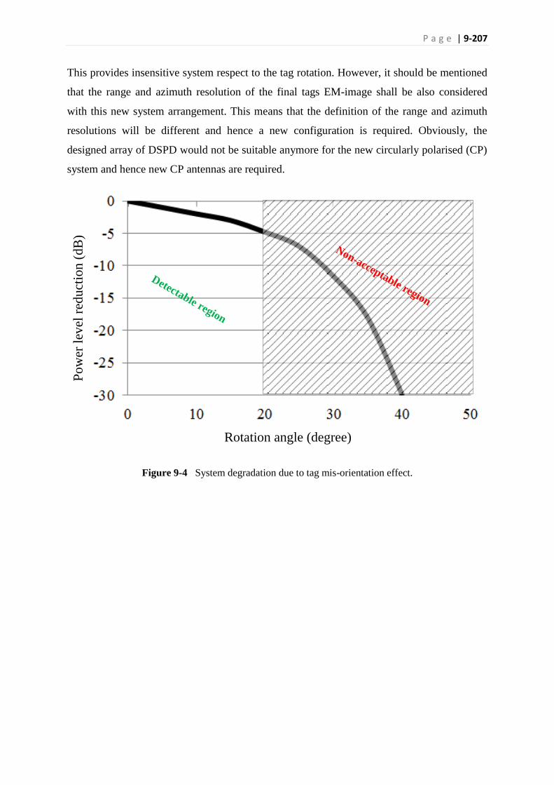
P a g e | 9-207
This provides insensitive system respect to the tag rotation. However, it should be mentioned
that the range and azimuth resolution of the final tags EM-image shall be also considered
with this new system arrangement. This means that the definition of the range and azimuth
resolutions will be different and hence a new configuration is required. Obviously, the
designed array of DSPD would not be suitable anymore for the new circularly polarised (CP)
system and hence new CP antennas are required.
Figure 9-4 System degradation due to tag mis-orientation effect.
Rotation angle (degree)
Pow
er l
evel
red
uct
ion (
dB
)
Detectable region
Non-acceptable region


208
REFRENCES
[1] P.Harrop and R.Das, "Printed and Chipless RFID Forecasts, Technologies & Players 2009-2029," IDTechEx, USA, 2009.
[2] BiQRious. (2015). QR Code Capacity. Available: http://qrcodetracking.com/qr-code-capacity/ [3] Barcode FAQ & Tutorial. Available:
http://www.idautomation.com/barcoding4beginners.html [4] C. Turcu, Current Trends and Challenges in RFID: InTech, 2011. [5] T.Lotlikar, R.Kankapurkar, A.Parekar, and A.Mohite, "Comparative study of Barcode, QR-
code and RFID System," International Journal Computer Technology & Applications,, vol. 4, pp. 817-821, 2013.
[6] E.Arendarenko, "A study of comparing RFID and 2D barcode tag technologies for pervasive mobile applications," Master, Department of Computer Science and Statistics, University of Joensuu, 2009.
[7] G. White, G.Gardiner, G. P. Prabhakar, and A. Razak, "A comparison of barcoding and RFID technologies in practice," Journal of Information, Information Technology and Organizations, vol. 2, pp. 119-132, 2007.
[8] Cartman. (Feb 2015). Asset Tracking: RFIDs, Barcodes or QR Codes? Available: https://www.webcheckout.net/blog/rfid-asset-tracking/
[9] A. Campbell. (2011). QR Codes, Barcodes and RFID: What’s the Difference? Available: http://smallbiztrends.com/2011/02/qr-codes-barcodes-rfid-difference.html
[10] Cisco. (2015). Internet-of-everything. Available: http://www.cisco.com/c/r/en/anz/internet-of-everything-ioe/tomorrow-starts-here/index.html
[11] S.Preradovic and N.Karmakar, "Chipless RFID, Bar Code of the Future," IEEE Microwave magazine, vol. 11, pp. 87-97, 2010.
[12] R. R. Fletcher. (2002). Low-cost electromagnetic tagging: Design and implementation. Ph.D. thesis. Available: www.media.mit.edu/physics/publications/theses/97.02.fletcher.pdf
[13] S.Preradovic, "Chipless RFID System for Barcode Replacement," PhD, ECSE, Monash University, 2009.
[14] V.Chawla and D. S. Ha, "An overview of passive RFID " Communications Magazine, IEEE vol. 45.
[15] P. Harrop. (2006). The Price-Sensitivity Curve for RFID. Available: http://www.printedelectronicsworld.com/articles/the-price-sensitivity-curve-for-rfid-00000488.asp?sessionid=1
[16] S.Preradovic, I.Balbin, N.C.Karmakar, and G.F.Swiegers, "Multiresonator-Based Chipless RFID System for Low-Cost Item Tracking," IEEE Transactions on Microwave Theory and Techniques, vol. 57, 2009.
[17] T. Singh, S. Tedjini, E. Perret, and A. Vena, "A Frequency Signature Based Method for the RF Identification of Letters," in 2011 IEEE international conference on RFID, 2011.
[18] A.Vena, E.Perret, and S. Tedjini, "Chipless RFID Tag Using Hybrid Coding Technique," IEEE Transactions on Microwave Theory and Techniques, vol. 59, 2011.
[19] C. S. Hartmann, "A Global SAW ID Tag with Large Data Capacity," in IEEE ULTrasonic Symposium, 2002.
[20] C.Mandel, B.Kubina, M.Schüßler, and R.Jakoby, "Metamaterial-inspired Passive Chipless Radio-frequency Identification and Wireless Sensing," Annals of telecommunications, vol. 68, pp. 385-399, 2013.
[21] C.Mandel, B.Kubina, M.Schussler, and R.Jakoby, "Group-delay Modulation with Metamaterial-inspired Coding Particles for Passive Chipless RFID," presented at the RFID-TA, Nice, 2012.

209
[22] S. Shrestha, M.Balachandran, M.Agarwal, and V.V.Phoha, "A Chipless RFID Sensor System for Cyber Centric Monitoring Applications," IEEE Transactions on Microwave Theory and Techniques, vol. 57, 2009.
[23] J.R.Costa, B.Lima, and C.A.Fernandes, "Compact Beam-Steerable Lens Antenna for 60-GHz Wireless Communications," IEEE Transactions on Antenna and Propagation, vol. 57, p. 8, 2009.
[24] H.El Matbouly, N.Boubekeur, and F.Domingue, "A Novel Chipless Identification Tag Based on a Substrate Integrated Cavity Resonator " IEEE Microwave and Wireless Components Letters, vol. 23, 2013.
[25] C.M.Nijas, R.Dinesh, U.Deepak, A.Rasheed, S.Mridula, K.Vasudevan, et al., "Chipless RFID Tag Using Multiple Microstrip Open Stub Resonators," IEEE Transactions on Antenna and Propagation, vol. 60, pp. 4429-4432, 2012.
[26] Y.F.Weng, S.W.Cheung, T.I.Yuk, and L. Liu, "Design of Chipless UWB RFID System Using A CPW Multi-Resonator," IEEE Antenna and Propagation Magazine, , vol. 55, 2013.
[27] M.Zomorrodi and N.C.Karmakar, "An Array of Printed Dipoles at 60 GHz " in IEEE International Symposium on Antennas and Propagation, Memphis, Tennessee, USA, July-2014, pp. 73-74.
[28] M.Zomorrodi and N.Karmakar, "A Low Cost Wideband Printed Dipole Array Antenna for 60 GHz Image-Based Chipless RFID Reader," IEEE Antennas and Propagation Magazine, vol. Accepted on Jan2015, p. 13, 2015.
[29] S.Gupta, B.Nikfal, and C.Caloz, "Chipless RFID System Based on Group Delay Engineered Dispersive Delay Structures," IEEE Antenna and Wireless Propagation letters, vol. 10, pp. 1366-1368, 2011.
[30] R.Rezaiesarlak and M.Manteghi, "Complex-Natural-Resonance-Based Design of Chipless RFID Tag for High-Density Data," IEEE transactions on Antenna And Propagation vol. 62, 2014.
[31] ACMA, "60 GHz Band, Millimetre Wave Technology," 2004. [32] S.K.Yong, "Introduction to 60 GHz," Samsung Electronics 2011. [33] S.Yong and C.Chong, "An Overview of Multi Giga bit Wireless through Millimeter Wave
Technology: Potentials and Technical Challenges," EURASIP Journal on Wireless Communications and Networking, p. 10, 2007.
[34] S.Yong, P.Xia, and A.V.Garcia, 60 GHz Technology for Gbps WLAN and WPAN: John&Wiley, 2011.
[35] D. L. Brock, "The Electronic Product Code (EPC)," Auto-ID center, massachusetts institute of technology(MIT)2001.
[36] M.Zomorrodi, N.C.Karmakar, and S.G.Bansal, "Introduction of Electromagnetic Image-based Chipless RFID System " in Intelligent Sensors, Sensor Networks and Information Processing, ISSNIP-2013, Melbourne, 2013, pp. 443-448.
[37] M.Zomorrodi and N.C.Karmakar, "On the Usage of Diffraction Effect for Chipless RFID Systems," in Australian Microwave Symposium (AMS), Melbourne, Australia, June 2014.
[38] (2015). Available: www.satoaustralia.com [39] M.Zomorrodi and N.C.Karmakar, "Cross-RCS Based, High Data Capacity, Chipless RFID
System," in International Microwave Symposium (IMS-2014), Tampa Bay, Flordia, US, 2014. [40] M.Zomorrodi and N.C.Karmakar, "Cross-Polarized Printable Chipless RFID Tag with Superior
Data Capacity," in European microwave week, EuMW2014, Rome, Italy, 2014. [41] T.Pisello, "The ROI of RFID in the Supply Chain," RFID Journal internet article, 2006. [42] U. o. Sanfrancisco. (Feb 2015). RFID Technology Boosts Walmart’s Supply Chain
Management. Available: http://www.usanfranonline.com [43] D. A. Hodges and H. G. Jackson, Analysis and Design of Digital Integrated Circuits 2nd ed.
New York, USA: McGraw-Hill, 1988. [44] J. R. Baker, H. W. Li, and D. E. Boyce, CMOS Circuit Design, Layout and Simulation. New York,
USA: IEEE Press, 1998.

210
[45] M. S. Bhuiyan, R.E. Azim, and N. Karmakar, "A Novel Frequency Reused Based ID Generation Circuit for Chipless RFID Applications," in Asia-Pacific Microwave Conference (APMC), Melbourne, Australia, 2011, pp. 1470-1473.
[46] I. Balbin and N.C.Karmakar, "Phase-Encoded Chipless RFID Transponder for Large-Scale Low-Cost Applications," IEEE Microwave and Wireless Components Letters,, vol. 19, pp. 509-511, AUGUST 2009.
[47] Md. Aminul Islam and N.C.Karmakar, "A Novel Compact Printable Dual-Polarized Chipless RFID System," IEEE Transactions on Microwave Theory and Techniques, vol. 60, pp. 2142-2151, July 2012.
[48] A. Ramos, A. Lazaro, D. Girbau, and R. Villarino, "Time-domain Measurement of Time-coded UWB Chipless RFID Tags," Progress In Electromagnetics Research, vol. 116, 2011.
[49] Z. Lu, S. Rodriguez, H. Tenhunen, and Z. Li-Rong, "An Innovative Fully Printable RFID Technology Based on High Speed Time-domain Reflections," in High Density Microsystem Design and Packaging and Component Failure Analysis, 2006, pp. 166-170.
[50] V.P Plessky and L.M.Reindl, "Review on SAW RFID Tags," IEEE Transactions on Ultrasonics, Ferroelectrics, and Frequency Control, vol. 57, pp. 14-23, 2010.
[51] C. Mandel, M. Schüßler, M. Maasch, and R. Jakoby, "A Novel Passive Phase Modulator Based on LH Delay Lines for Chipless Microwave RFID Applications," in IEEE MTT-S International Microwave Workshop on Wireless Sensing, Local Positioning, and RFID, Crotia, 2009.
[52] F.J.H.Martínez, F.Paredes, and G.Zamora, "Printed Magnetoinductive-Wave (MIW) Delay Lines for Chipless RFID Applications," IEEE Transactions on Antennas and Propagation vol. 60, 2012.
[53] A.Chamarti and K.Varahramyan, "Transmission Delay Line Based ID Generation Circuit for RFID Applications," IEEE Microwave and Wireless Components Letters, vol. 16, pp. 588-590, Nov. 2006.
[54] M.Sch¨ußler, C.Damm, M.Maasch, and R.Jakoby, "Performance Evaluation of Left-Handed Delay Lines for RFID Backscatter Applications," in Microwave Symposium Digest, , 2008.
[55] J.Vemagiri, A.Chamarti, M.Agarwal, and K.Varahramyan, "Transmission Line Delay-Based Radio Frequency Identification (RFID) tag," Microwave and Optical Technology Letters, vol. 49, p. 1900, 2007.
[56] (14 July 2014). RF SAw Inc. Available: http://www.rfsaw.com [57] S.Preradovic, I.Balbin, N.C.Karmakar, and G.Swiegers, "Chipless Frequency Signature Based
RFID Transponders," in 1st European Wireless Technology Conference, Amsterdam 2008, pp. 302-305.
[58] D.Girbau, J.Lorenzo, A.Lázaro, C.Ferrater, and R.Villarino, "Frequency-Coded Chipless RFID Tag Based on Dual-Band Resonators," IEEE Antennas and Wireless Propagation Letters, vol. 11, 2012.
[59] F.Costa, S.Genovesi, and A.Monorchio, "A Chipless RFID Based on Multiresonant High-Impedance Surfaces," IEEE Transactions on Microwave Theory and Techniques, vol. 61, 2013.
[60] S.Mukherjee and G.Chakraborty, "Chipless RFID Using Stacked Multilayer Patches," in Applied Electromagnetics Conference (AEMC), 2009 Kolkata, 2009.
[61] M. Glickstein, "Firewall Protection for Paper Documents, ," RFID Journal internet article, 2004.
[62] K. C. Jones, "Invisible RFID Ink Safe For Cattle And People, Company Says," InformatioWeek, 2007.
[63] St. Louis, "SOMARK's Chipless RFID Ink Tattoo Field Demo Brings the Company Closer to Launch," 2008.
[64] S.Kim, A.Georgiadis, A.Collado, and M.M. Tentzeris, "An Inkjet-Printed Solar-Powered Wireless Beacon on Paper for Identification and Wireless Power Transmission Applications," IEEE transactions on microwave theory and techniques, vol. 60.

211
[65] I.Jalaly and I.D.Robertson, "RF Barcodes Using Multiple Frequency Bands," in International Microwave Symposium Digest, IEEE MTT-S 2005.
[66] I.Balbin, "Chipless RFID transponder design," PhD, Monash Univeristy, 2010. [67] H.S.Jang, W.G. Lim, K.S. Oh, S.M. Moon, and J.W. Yu, "Design of Low-Cost Chipless System
Using Printable Chipless Tag With Electromagnetic Code," IEEE Microwave and Wirless Components letters, vol. 20, 2010.
[68] B.A.Munk, Frequency Selective Surfaces, Theory and Design: John Wiley & Sons Inc, 2000. [69] M. G. Pettus, "RFID system utilizing parametric reflective technology " USA Patent, 2005. [70] S.Särkkä, V. E, V. Viikari, M.Huusko, and K. Jaakkola, "Phase-Based UHF RFID Tracking With
Nonlinear Kalman Filtering and Smoothing " IEEE Sensors Journal, vol. 12, 2012. [71] P. V.Nikitin, R.Martinez, S.Ramamurthy, H.Leland, G.Spiess, and K. V. S. Rao, "Phase Based
Spatial Identification of UHF RFID Tags," presented at the IEEE RFID, 2010. [72] A.Vena, E.Perret, and S.Tedjini, "Chipless RFID Tag Using Hybrid Coding Technique," IEEE
Trans. on Microwave Theory and Tech. , vol. 59, 2011. [73] Md. S. Bhuiyan, A.Azad, and N.Karmakar, "Dual-band Modified Complementary Split Ring
Resonator (MCSRR) Based Multi-resonator Circuit for Chipless RFID Tag " in IEEE- Intelligent Sensors, Sensor Networks and Information Processing,, Melbourne,Australia, 2013.
[74] M. Soumekh, Synthetic Aperture Radar signal processing with MATLAB algorithms. USA: John Wily and Sons 1999.
[75] P.Treleaven and J.Wells, "3D Body Scanning and Healthcare Applications," IEEE Computer Society, vol. 40, p. 28, 2007.
[76] S. Oka, H. Togo, N. Kukutsu, and T. Nagatsuma, "Latest Trends in Millimetre-Wave Imaging technology," Progress In Electromagnetics Research Letters,, vol. 1, pp. 197–204, 2008.
[77] A. A. Bakar, "Design of Ultra-Wideband Microwave Imaging System for Breast Cancer Detection and Its Assessment Using Heterogeneous Breast Phantoms," PhD, School of Information Technology and Electrical Engineering, The University of Queensland, Brisben, March 2012.
[78] F. Ahmad, M.G. Amin, and S. A. Kassam, "Synthetic Aperture Beamformer for Imaging Through a Dielectric Wall," IEEE Transactions on Aerospace and Electronic Systems, vol. 41, 2005.
[79] N.Karmakar, R.Kosowatta, P.Kalansuriya, and R. E-Azim, Chipless RFID Reader signal Processing: Artech House Publishing, 2013.
[80] M.Skolnic, Radar Handbook, 3rd ed.: McGraw-Hill, 2008. [81] G.L.Charvat, A Low-Power Radar Imaging System: Michigan State University, 2007. [82] M.Zomorrodi and N.Karmakar, "Novel MIMO-based Technique for EM-imaging of Chipless
RFID " in International microwave synposium (IMS-2015), 17-22 May 2015, Phoenix, USA. [83] U. 6400. (2015). 60 GHz transciver. Available: http://www.siliconimage.com/ [84] C.M.Ta and B.N. Wicks, "Issues in the Implementation of a 60GHz Transceiver on CMOS," in
IEEE International Workshop on Radio-Frequency Integration Technology(RFIT), Rasa Sentosa Resort, USA, 2007, pp. 135 - 140
[85] M.Zomorrodi and N. Karmakar, "A Low Cost Wideband Printed Dipole Array Antenna for 60 GHz Image-Based Chipless RFID Reader”," IEEE Antennas and Propagation Magazine, 2014.
[86] E.Md.Amin, Md.S.Bhuiyan, N.C.Karmakar, and B.Winther-Jensen, "Development of a Low Cost Printable Chipless RFID Humidity Sensor," IEEE Sensors Journal, vol. 14, pp. 140-149, 2014.
[87] C. A. Wiley, "Synthetic Aperture Radars: A Paradigm for Technology Evolution," IEEE Transactions on Aerospace and Electronic Systems,, vol. AES-21, p. 4, May 1985.
[88] JPL. Available: http://southport.jpl.nasa.gov/ [89] A.T.Blischack and M.Manteghi, "Embeded Singularity chipless RFID Tags," IEEE transactions
on Antenna And Propagation, vol. 59, Nov2011 2011.

212
[90] N. C. Karmakar, Handbook of Smart Antennas for RFID Systems. Singapore: John Wiley, 2010.
[91] ITU-R, "Rec.p 676-9, Attenuation by Atmospheric Gases," International Telecommunication Union, Geneva2012.
[92] C.Koh, "The Benefits of 60 GHz Unlicensed Wireless Communications," YDI Company, USA. [93] ITU, Radio Regulation. Geneva: ITU, 2012. [94] N.Guo, R.C.Qiu, Sh.S.Mo, and K.Takahashi, "60-GHz Millimeter-Wave Radio: Principle,
Technology, and New Results," EURASIP Journal on Wireless Comm. and Networking, 2007. [95] W. Buchar, N. Karmakar, and M.Zomorrodi, "MIMO-Based Technique for Chipless RFID EM-
Imaging at 60 GHz," Grant proposal Xerox, USASep 2014. [96] Available: http://www.kurz.de [97] M. H.Williams, "Diffraction by a Finitie Strip," Oxford Journals, Mathematics & Physical
Sciences, vol. 35, 1980. [98] M.C.Heaton, P.J.Joseph, and R.L.Haupt, "Unifrom Theory of Diffraction Analysis for
Conductive Strips with Constant and Tapered Resistive Loads," in Antennas and Propagation Society International Symposium, , 1991, p. 4.
[99] U.Y.Ziya, "Physical Optics Theory for the Scattering of Waves by an Impedance Strip," Optics Communications, vol. 284, p. 1760, 2010.
[100] R.G.Kouyoumjian and P.H.Pathak, "A Unifm Geometrical Theory of Diffraction for an Edge in a Perfectly Conducting Surface," Proceeding of the IEEE, vol. 62, 1974.
[101] S.W.Lee, "Comparison of Uniform Asymptotic Theory and Ufimtsev’s Theory of Electromagnetic Edge Diffraction," IEEE Transactions on Antennas and Propagation, vol. 25, 1977.
[102] T.Griesser and C.A.Balanis, "Backscatter Analysis of Dihedral Corner Reflectors Using Physical Optics and the Physical Theory of Diffraction," IEEE Transactions on Antennas and Propagation, vol. 35, 1987.
[103] R.Mittra, Y.Rahmat-Samii, and W. L. Ko, "Spectral Theory of Diffraction," Applied Physic, vol. 10, 1976.
[104] V.C.Monk and F.W.Sedenquist, "High-Frequency Radar Modeling," Advanced Sensors Directorate Research, Development, and Engineering Center, Alabama1995.
[105] J.B.keller, "One Handred Years of Diffraction Theory," IEEE Transactions on Antennas and Propagation, vol. AP-33, p. 4, 1985.
[106] A.Imran and Q.A.Naqvi, "Diffraction of Electromagnetic Plane Wave from a Slit in a PEMC Plane," Progress In Electromagnetics Research vol. 8, 2009.
[107] M.A.Imran, "Diffraction of Electromagnetic Plane Waves from Strips and Slits Using the Method of Kobayashi Potential," PhD Thesis, Quaid-I-Azam University, Islam Abad, 2010.
[108] A.K.Bhattacharyya and T.J.Chwalek, "Analysis of Multilayered Meander Line Polarizer," International Journal of Microwave and Millimeter-Wave Computer-Aided Engineering, vol. 7, pp. 442-454, 1997.
[109] L.Young, L.A.Robinson, and C.A.Hacking, "Meander-line Polarizer," IEEE Transactions on Antennas and Propagation, May-1973.
[110] R.S.Chu and K.Lee, "Analytical Model of a Multilayered Meander-Line Polarizer Plate with Normal and Oblique Plane-Wave Incidence," IEEE Transactions on Antennas and Propagation, vol. 35, p. 652, 1987.
[111] M.Mazur and W.Zieniutycz, "Multi-layer Meanderline Polarizer for Ku-band," in Microwave, Radar and wireless communications(MIKON-2000), p. 78.
[112] F.Jian, "The Optimum Designing Method for Wide Bandwidth Meander-line Circular Polarizer " in Antennas, Propagation and EM Theory, ISAPE 2000, pp. 10-13.
[113] ACMA, "LIPD Regulation," 2011. [114] (Sep 2014). Available: http://www.satoaustralia.com/

213
[115] W.Wiesbeck and D.Kahny, "Single Reference, Three Target Calibration and Error Correction for Monostatic Plarimetric Free Space Measurements," Proceedings of the IEEE, vol. 79, pp. 1551-1558, 1991.
[116] A.Vena, E.Perret, and S.Tedjni, "A Depolarizing Chipless RFID Tag for Robust Detection and Its FCC Compliant UWB Reading System," IEEE Transactions on Microwave Theroy and Technique, vol. 61, pp. 2982-2995, 2013.
[117] (2014, Oct 2014). Vector network analyser. Available: http://www.agilent.com [118] J.Siden, P.Jonsson, T.Olsson, and G.Wang, "Performance Degradation of RFID System Due to
the Distortion in RFID Tag Antenna," in Microwave and Telecommunication Technology,, Sevastopol,Ukraine, 2001, pp. 371-373.
[119] ACMA, "Radiocommunications (Low Interference Potential Devices) Class Licence 2000," ACMA, Canberra2011.
[120] Nokia. (14 Oct 2014). Radio Link Systems Nokia MetroHopper 58 GHz. Available: www.comlab.hut.fi/studies
[121] (14 Oct 2014). Terabeam product. Available: http://www.proxim.com/ [122] A.Nesic, S.Jovanovic, and V.Brankovic, "Design of Printed Dipoles Near The Third
Resonance," in Antennas and Propagation Society International Symposium, , Atlanta, GA, USA 1998, pp. 928-931.
[123] R.B.Waterhouse, D.Novak, A.Nirmalathas, and C.Lim, "Broadband Printed Sectorized Coverage Antennas for Millimeter-Wave Wireless Applications," IEEE Transactions on Antennas and Propagation, vol. 50, pp. 12-16, 2002.
[124] W.Menzel, "A 40 GHz Printed Array Antenna," in Digest, 1980, pp. pp. 225-226. [125] C.Peixeiro, P.Dufrane, and Y.Gullerme, "Microstrip Patch Antennas for a Mobile
Communications System at 60 GHz," in Antennas and Propagation Society International Symposium, AP-S. Digest Baltimore, MD, USA 1996
[126] T.G.Ma and S.K.Jeng, " A Printed Dipole Antenna with Tapered Slot Feed for Ultrawide Band Applications,," IEEE Transactions on Antennas and Propagation, vol. 53, pp. 3833–3839, 2005.
[127] M.Scott, "A Printed Dipole for Wide-Scanning Array Application," in IEEE 11th Int. Conference on Antennas and Propagation, 2001, pp. 37-40.
[128] Y.Ho.Suh and K.Chang, "A New Millimeter-Wave Printed Dipole Phased Array Antenna Using Microstrip-Fed Coplanar Stripline Tee Junctions," IEEE Transactions on Antennas and Propagation, vol. 52, pp. 2019-2027, Aug 2004.
[129] V.Brankovic and A.Nesic, "Wide Band Printed Phase Array Antenna for Microwave and mm-Wave Applications," US Patent, March 2000.
[130] R.A.Alhalabi and G.M.Rebeiz, "High-Efficiency Angled-Dipole Antennas for Millimeter-Wave Phased Array Applications," IEEE Transactions on Antennas and Propagation, vol. 56, p. 7, 2008.
[131] Y.C.Chiou, R.A.Alhalabi, and G.M.Rebeiz, "High-Efficiency 60 GHz Dipole-Box Antennas," in Antennas and Propagation Society International Symposium (APSURSI), , 2010.
[132] P.Kalansuriya, N.CKarmakar, and E. Viterbo, "On the Detection of Frequency-Spectra-Based Chipless RFID Using UWB Impulsed Interrogation," IEEE Transactions on Microwave Theory and Techniques,, vol. 60, 2012.
[133] Taconic, "Taconic laminate material guide," ed, 2014. [134] R. Anita and M.V.C.Kumar, "Analysis of Triangular Microstrip Patch Antenna for Different
Antenna," in JREAT International Journal of Research in Engineering & Advanced Technology, 2013.
[135] S.Dey and N.C. Karmakar, "Design of Novel Super Wide Band Antennas close to the Small Antenna Limitation Theory " in Microwave Symposium (IMS), 2014 IEEE MTT-S International Tampa, FL, 2014, pp. 1-4.

214
[136] H.R.Fettermana, T.C.L.G.Sollnera, P.T.Parrisha, D.Parkera, H.Mathewsa, and P.E.Tannenwalda, "Printed Dipole Millimeter Antenna for Imaging Array Applications," Electromagnetics, vol. 3, pp. 209-215, 1983.
[137] D.M.Pozar, "Considerations for Millimeter Wave Printed Antennas," IEEE Transactions on Antennas and Propagation, vol. 31, No 5, p. 8, 1983.
[138] P.Katehi and N.Alexopoulos, "On the Effect of Substrate Thickness and Permittivity on Printed Circuit Dipole Properties " IEEE Transactions on Antennas and Propagation, vol. 31, p. 6, Jan 1983.
[139] W.Hong and K.Wu, "94 GHz Substrate Integrated Monopulse Antenna Array," IEEE Transactions on Antennas and Propagation, vol. 60, pp. 121-129, 2011.
[140] D.E.Zelenchuk, V.Fusco, G.Goussetis, A.Mendez, and D.Linton, "Millimeter-Wave Printed Circuit Board Characterization Using Substrate Integrated Waveguide Resonators," IEEE Transactions on Microwave Theory and Technique, vol. 60, Oct 2012.
[141] M.Bozzi and L.Perregrini, "Modeling of Conductor, Dielectric, and Radiation Losses in Substrate Integrated Waveguide by the Boundary Integral-Resonant Mode Expansion Method," IEEE Transactions on Microwave Theory and Techniques, vol. 56, pp. 3153-3161, 2008.
[142] J.Sheen, "Comparisons of Microwave Dielectric Property Measurements by Transmission/Reflection Techniques and Resonance Techniques " Measurement Science and Technology, vol. 20, 2009.
[143] W.L.Stutzman and G.A.Thiele, Antenna Theory and Design: John Wiley&Sons, 1981. [144] C.A.Balanis, Antenna Theory Analysis and Design, Third ed.: John Wiley&Sons, 2005. [145] G.Y.Chen and J.Sh.Sun, "A Printed Dipole Antenna with Microstrip Tapered Balun,"
Microwave and Optical Technology Letters, vol. 40, pp. 344-346, 20 Feb 2004. [146] R.J. P.Douvilie and D.S.James, "Experimental Study of Symetric Microstrip Bends and Their
Compensation," IEEE Transactions on Microwave Theory and Technique vol. 26, p. 175, 1978. [147] S.M.Roy, "Development of a Frequency Encoded Chipless RFID Tag," PhD, ECSE, Monash
University, 2008. [148] R.L.Haupt, Antenna Arrays, A Computational Approach. Pennsylvania State University, State
College, Pennsylvania: John Wiley&Sons, Inc, Publication, 2010. [149] D. M. Pozar, Microwave Engineering, Third ed.: John Wiley&Sons, 2005. [150] J. Coonrod, "Comparing Microstrip and CPW Performance," Microwave Journal, vol. 55, pp.
74-82, July 2012. [151] S. Microwave. 1.85 mm connectors. [152] (2013). SouthWest Microwave. Available: www.southwestmicrowave.com [153] Ainfoinc Company. Available: http://www.ainfoinc.com [154] W.Carrara, R.Goodman, and R.Majewski, Spotlight Synthetic Aperture Radar Signal
Processing Algorithm. Boston,: Artesch House, 1995. [155] L. Martin. 3 dimensional radar. Available:
http://www.lockheedmartin.com.au/us/products/ground-based-air-surveillance/3delrr.html [156] A.Vettore, S.Ponte, and N.Crocetto, "Space-Based Surface Change Detection with
Differential SAR Interferometry: Potentials and Preliminary Investigations," in Symposium on geospatial theory, processing and applications, Ottawa, Canada, 2002.
[157] L.J.Cutrona, "A Comparision of Techniques for Achieving Fine Azimuth Resolution," IRE Transactions on Military Electronics, vol. MIL-6, pp. 119-121, 1962.
[158] M. A. Islam, "PhD Transfer Report, Compact Printable Chipless RFID System Using
Polarization Diversity," Monash University, Melbourne2010. [159] "Brochure on RFID-Radar™ System," T. S. P. Ltd, Ed., ed. Johannesburg,South Africa, 2011. [160] A. Jamod, V. D. R. Gopu, and Y. S. Rao, "Matlab based SAR signal processor for educational
use," in Geoscience and Remote Sensing Symposium (IGARSS), 2012 IEEE International MUNICH, 2012, pp. 5318 - 5321

215
[161] R. Bamler, "A comparision of Range-doppler and wavenumber domain SAR focusing algorithm," IEEE Transactions on Geoscience And Remote Sensing, vol. 30, 1992.
[162] A.AV.Uppuluri and R.J.Jost, "Matlab-based ERS SAR Data Acquisition and Processing Software for Classroom use," in IEEE International Radar Conference, 2004.
[163] M.Zomorrodi, "Improved Genetic Algorithm approach for Phased Array Radar Design," in The Asia-Pacific Microwave Conference, APMC, melbourne, Australia, 2011, pp. 1850-1854.
[164] Y.Yu, P.G. M. Baltus, A.Graauw, E. der Heijden, and C.S.Vaucher, "A 60 GHz Phase Shifter Integrated With LNA and PA in 65 nm CMOS for Phased Array Systems," IEEE Jornal of Solid-State Circuits, vol. 45, 2010.
[165] J. Li and P. Stoica, MIMO Radar Signal Processing: JohnWiley& Sons, NY, USA, 2008. [166] W. Q. Wang, "Virtual Antenna Array Analysis for MIMO Synthetic Aperture Radars,"
International Journal of Antennas and Propagation, Hindawi Publishing Corporation, vol. 2012, p. 10, 2012.
[167] A. M. Haimovich, R. S. Blum, and L. J. Cimini, "MIMO radar with widely separated antennas," IEEE Signal Processing Magazine, vol. 25, pp. 116-129, 2008.
[168] X. Zhuge and A. G. Yarovoy, "A sparse aperture MIMO-SAR based UWB imaging system for concealed weapon detection," IEEE Transactions on Geoscience and Remote Sensing, vol. 49, pp. 509-518, 2011.
[169] correl Bill, "Efficient Spotlight SAR MIMO Linear Collection Configurations," IEEE journal of selected topics in signal processing, vol. 4, p. 7, Feb 2010.
[170] D. R. Fuhrmann, J. P. Browning, and M. Rangaswamy, "Signaling strategies for the hybrid MIMO phased-array radar," IEEE Journal on Selected Topics in Signal Processing, vol. 4, pp. 66-78, 2010.
[171] Lincoln Laboratory, "Practical phased array antenna," Massachusetts Institute of Technology (MIT), Boston,2014.
[172] M.Zomorrodi, "A phased array antenna design with Genethic algorithm," MSc., Electrical Engineering school, K.N.Toosi, Tehran, Iran, 2000.
[173] Y. Rahmat-Samii and E. Michielssen, Electromagnetic Optimization by Genetic Algorithms: Wiley, 1999.