Embed Size (px)
DESCRIPTION
Mitsubishi PCL-ACUP-QCPU
Citation preview
− 1 −
Type ACPU (Common Instructions) Programming Manual IB-66250c
V. P. DATA Floppy Section Manual page NO.
File name Floppy NO. Designer data file name
1 1-1 to 1-3 010000cc 2-1 to 2-4 020000cc 2+, 2+P, 2+2, 2+p2, 2-, 2-P, 2-2, 2-P2, 2002abc
2-5 to 2-7 020202cc LD, LDI, AND, ANI, OR, ORI, ANB, ORB, MPS, MRD, MPP, OUT, SET, RST, PRS, RLF, CHK, SFT, SFTP, MC, MCR, FEND, END, ATOP, NOP
2-8 to 2-9 020203-1
2002abc, LD=, AND=, OR=, LD-ab, AND-ab, OR-ab, LD-b, AND-b, OR-b, LD-a=, AND-a=, OR-a=, LD-a, AND-a, OR-a, LD-b=, AND-b=, OR-b=, LDD=, ANDD=, ORD=, LDD-ab, ANDD-ab, ORD-ab, LDD-b, ANDD-b, ORD-b, LDD-a=, ANDD-a=, ORD-a=, LDD-b=, ANDD-b=, ORD-b=
2-10 to 2-12 020203-2
+, +P, +2, +P2, -, -P, -2, -P2, D+, D+P, D+2, D+P2, D-, D-P, D-2, D-P2, 2, 2P, 1, 1P, D2, D2P, D1, D1P, B+, B+P, B+2, B+P2, B-, B-P, B-2, B-P2, DB+, DB+P, DB+2, DB+P2, DB-, DB-P, DB-2, DB-P2, B2, B2P, B1, B1P, DB2, DB2P, DB1, DB1P, INC, INCP, DINC, DINCP, DEC, DECP, DDEC, DDECP, 2002abc
2-13 to 2-15 020203-3
BCD, BCDP, DBCD, DBCDP, BIN, BINP, DBIN, DBINP, MOV, MOVP, DMOV, DMOVP, CML, CMLP, DCML, DCMLP, BMOV, BMOVP, FMOV, FMOVP, XCH, XCHP, DXCH, DXCHP, CJ, SCJ, JMP, CALL, CALLP, RET, EI, DI, IRET, SUB, SUBP, CHG, COM, SEG, 2002abc
2-16 to 2-18 020204-1
WAND, WANDP, WAND2, WANDP2, DAND, DANDP, WOR, WORP, WOR2, WORP2, DOR, DORP, WXOR, WXORP, WXOR2, WXORP2, DXOR, DXORP, WXNR, WXNRP, WXNR, WXNRP, DXNR, DXNRP, NEG, NEGP, ROR, RORP, RCR, RCRP, ROL, ROLP, RCL, RCLP, DROR, DRORP, DROL, DROLP, DRCL, DRCLP
2-19 to 2-20 020204-2 SFR, SFRP, SFL, SFLP, BSFR, BSFRP, BSFL, BSFLP, DSFR, DAFL, DSFLP, SER, SERP, SUM, SUMP, DSUM, DSUMP, DECO, DECOP, ENCO, ENCOP, SEG, BSET, BSETP, BRST, BRSTP, D15, DISP, UNI, UNIP, ASC
2
2-21 to 2-24 020204-3
FIFW, FIFWP, FIFR, FIFRP, FROM, FROMP, DFRO, DFROP, TO, TOP, DTO, DTOP, FROM2, FROMP2, DFRO2, DFROP2, TO2, TOP2, DTO2, DTOP2, FOR, NEXT, LRDP, LWTP, RFRP, RTOP, PR, PRC, LED, LEDA, LEDB, LEDC, LEDR, WDT, WDTP, CHK, SLT, SLTR, STRA, STRAR, STC, CLC, DUTY, DSFRP, PSFLP
3-1 to 3-5 030000cc 3001a, 3001b, 3003a, 3003c, 3004b, 3004d, 3004e, 3005b, 3005d, 3005f
3-6 to 3-11 030300cc #0101, #0102, #0201, #0202, #0314, #0315, 3008b, 3008d, 3009b, 3009e
3-12 to 3-15 030600cc #0101, #0102, #0109, 0111
3
3-16 to 3-20 030802cc #0410, #2, #3, #5-2 4 4-1 to 4-3 040000cc
5-1 to 5-4 050000cc #5-1, #4-2, #3-2 5-5 to 5-8 050200cc 0008, #0328, #2, #4-2
5-9 to 5-13 050202cc 0009, #3-2, #9, #5-13 5-14 to 5-18 050300cc 0011, #0322, #0323, #0324, #0413 5-19 to 5-22 050302cc 0034, #2, 5019b, #1, 5020c, #3-3, 5021b, #5-2 5-23 to 5-26 050303cc 0034, #0101, 5023b, 5023d, 5024b, 5024d, 5024f, 0038, 5026b, 5-27 to 5-28 050400cc #0515, 5027b, #0604, 5028b, 0034 5-29 to 5-32 050500cc 0046, #7, 5029a, #1501, 5031a, #1001, 5031b, #1301, 5032a,
5-33 to 5-36 050600cc 0027, 5033a, #0605, 0005, 5035a, 5036a
5
5-37 to 5-38 050700cc 0030, 5037a, #0326
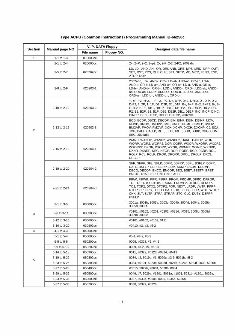
− 2 −
Type ACPU (Common Instructions) Programming Manual IB-66250c
V. P. DATA Floppy Section Manual page NO.
File name Floppy NO. Designer data file name
5-39 to 5-40 050702-1 0006, #0112, #0113, #0215, #0216, #0217, #0327 5
5-41 050702-2 03a 6-1 to 6-3 060000cc 6003a, 6003c, 6003e 6-4 to 6-7 060101cc 0004, #1, #2 6-8 to 6-12 060200cc 6009a, 6009b, 0010, 6010a, 6010b, 6011a, 6011b, 7004a, #1, #3
6-13 to 6-15 060202cc 0010, 6013a, 6013b, 6014a, 6014b, 7004a, #0102 6-16 to 6-18 060203cc 0016, 6016a, 6017a, 7004a, #0102, #0202 6-19 to 6-20 060204-1 #0101, 6072c, #0102, 0016, 6019a, 6020a, 7004a
6-21 060204-2 #0102, #0308 6-22 to 6-24 060205cc 0010, 6023a, 6023b, 7004a, #3, #1 6-25 to 6-27 060206cc 0010, 6025a, 6025b, 6026a, 6026b, 7004a, #3
6-28 to 6-30 060207cc 0016, 6028a, 6028b, 7004a, 6029c, #1, #2, 6030b 6-31 to 6-33 060208cc 6031a, 6031b, 6032a, 6032b, 6033b, 6033d, 0016, #1, #2, 7004a
6-34 to 6-37 060209cc 0034, 6034a, 6034b, 7004a, #0404, #0310, 6036a, 6036b, #0109, #0203
6-38 to 6-41 060300cc 0039, 6039a, 6039b, 6040a, 6040b, 7004a, 6041a, 6041b, #1, #3
6-42 to 6-45 060302cc 6042a, 6042b, 6043a, 6043b, #1, #3, 6044a, 6045a, 0039, 7004a, #5
6-46 to 6-48 060400cc 0039, 6047a, 6047b, #0101, 6048d 6-49 to 6-50 060402-1 0039, 6049a, 6049b, 6050a, 6050b, 6050c
6-51 060402-2 6051a, 6051b, 6051f 6-52 to 6-54 060403cc 0016, 6052a, 6053a, 7004a, 6054a, 6054b, #1, 6055a, 6055b 6-56 to 6-57 060404cc 0039, 6056a, 6056b, 7004a, #1
6-58 to 6-61 060500cc 0058, 6058a, 6058b, #0405, #0406, #0509, #0407, #0312, #0408 6-62 to 6-63 060502cc 0062, 6062a, #4, 6063b, #7 6-64 to 6-66 060503cc 0064, 6064a, #3, 6065b, #5 6-67 to 6-68 060504cc 0034, 6067a, #2, 7004a 6-69 to 6-71 060600-1 0061, 6069a, 6669a, 6070a, #0110, 6071a 6-72 to 6-73 060600-2 #0101, 6072a, 6072c
6-74 to 6-75 060600-3 #0102, 6072c 6-76 to 6-78 060600-4 #0111, 6077a, 6077a-1, 6076c, 6070a-1 6-79 to 6-81 060600-5 #0111, 6070a-2, #0703, #0603, #0209
6-82 to 6-85 060700cc 0027, 6082a, 6083a, 6083b, 6083c, 0084, 6084a, 6084b, 6084c, 6085a, #8
6
6-86 to 6-89 060703cc 0086, #2, #5-2 7-1 to 7-2 070000cc 7-3 to 7-6 070101cc 0010, 7003a, 7003b, 7004a, 7004b, #1, #2, 7005a, 7005b, 7006a 7-7 to 7-10 070102cc 0010, 7007a, 7007b, 7008a, 7004a, #1, #2 7-11 to 7-14 070103cc 0010, 7011a, 7011b, 7012a, 7004a, #1, #2, #3
7-15 to 7-18 070104cc 0010, 7015a, 7015b, 7016a, 7004a, #5, #1, #3 7-19 to 7-20 070105cc 0034, 7019a, 7004a, #3 7-21 to 7-23 070200cc 0034, 7022a, 7022b, 7004a, 7023a, 7023b
7-24 to 7-27 070202cc 0034, 7024a, 7024b, 7004a, 7025a, 7025b, 7026a, 7026b, 7027a, 7027b
7
7-28 to 7-29 070204cc 0034, 7028a, 7028b, 7004a, 7029b, 7029d

− 3 −
Type ACPU (Common Instructions) Programming Manual IB-66250c
V. P. DATA Floppy Section Manual page
NO. File name Floppy NO. Designer data file name
7-30 to 7-32 070300cc 0039, 7031a, 7031b, #0101, 7732, 7732c, 0039
7-33 to 7-36 070302cc 7733a, 7733b, 7734, #0101, 0039, 7035a, 7035b, 7004a, 7736a, 7736b,
7-37 to 7-39 070400cc 0016, 7004a, #0102
7-40 to 7-43 070402cc 0034, 7040a, 7040b, 7004a, #0101, 7041a, #0401, 7041b, 0016, #0102, 7043a, 7043b
7-44 to 7-45 070404cc 0086, 7044a, 7045a, #0101, 7045d 7-46 to 7-47 070405cc 0039, #0103, 7046a, 7046b, 7004a, #0214, 7047a 7-48 to 7-50 070406cc 0016, 7048a, 7049a, 7004a, #0102, 7049b, 7050a 7-51 to 7-52 070407cc 0037, 7051a, 7051b, #0202 7-53 to 7-54 070500-1 7754, 0039
7-55 to 7-57 070500-2 7754, 7004a, #0204, 7056b, 7057a 7-58 to 7-60 070600cc 0017, 7059a, 7060a, 7004a, #1 7-61 to 7-62 070602cc 0017, 7067a, 7060a, 7004a, #1 7-63 to 7-66 070603cc 0018, 7059a, 7064a, 7064b, 7065a, 7066a, #2-2 7-67 to 7-68 070604-1 0019, 7067a, 7064a, 7064b 7-69 to 7-70 070604-2 7065a, 7066a, #2-2
7-71 to 7-73 070605cc 0017, 7071a, 7004a, #1 7-74 to 7-76 070606cc 0017, 7074a, 7004a, #1 7-77 to 7-78 070700cc 0035, #0901, #0701 7-79 to 7-85 070800cc 0017, 7074b, #1, 7075a, #6, 7076b, 7074b, 7078a, 7076b 7-86 to 7-88 070802-1 0017, 7080a, #1, 7081b, #5, 7084b 7-89 to 7-91 070802-2 #1, 7083b, #5, 7084b, 7085a, 7085b, 7085c
7-92 to 7-93 070900cc 7087a 7-94 to 7-96 070901-1 0038, 7089a, 7090a 7-97 to 7-99 070901-2 7091a, 7092c, 7081b, #0402, #0303, 7093c, 7093b
7-100 to 7-102 070902cc 0033, 7094a, 7751b, #0304, #0503 7-103 to 7-107 070903cc 0045, 7097a, 7751b, #0201, 0030, 7100a, 7100b, 7051b 7-108 to 7-110 071000cc 0031, 7102a, 7004a, 7103b
7-111 to 7-113 071002-1 0059, #4, 7106a, #1401 7-114 to 7-116 071002-2 #1, 7108a, 7109a, 7109b, 7110a, 7110b, 7110c, 7110d, 7110e 7-117 to 7-120 071003cc 0029, 7111a, 7114a 7-121 to 7-124 071005cc 0029, 7115a, #5, 0015, 7117a, #1, 7118b 7-125 to 7-129 071100cc 0038, 7120a, 7120b, 7121a, 7125b, 7121b, #0505, #0602
7
7-130 to 7-133 071102cc 0038, 7124a, 7125a, #0506, #0507 8-1 to 8-3 080000cc 8002a
8-4 to 8-7 080300cc 0033, 8005a, 0034, 8005b, 8006a, 8006b
8-8 to 8-12 080304-1 8007a, 8007b, 8007c, 8008a, 8009a, 8010a, 8010b, 8007d, 8010c
8
8-13 to 8-16 080304-2 8011a, 8009a 9-1 to 9-5 090000cc 9002a, 9002b 9-6 to 9-9 090300-1 0033a
9-10 to 9-12 090300-2 9
9-13 to 9-16 090400-1 0033a
− 4 −
Type ACPU (Common Instructions) Programming Manual IB-66250c
V. P. DATA Floppy Section Manual page NO.
File name Floppy NO. Designer data file name
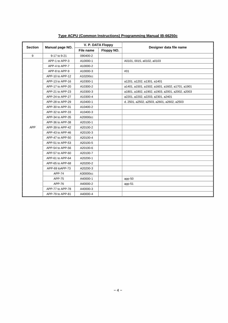
9 9-17 to 9-21 090400-2 APP-1 to APP-3 A10000-1 A0101, 0015, a0102, a0103 APP-4 to APP-7 A10000-2 APP-8 to APP-9 A10000-3 #01
APP-10 to APP-12 A10200cc
APP-13 to APP-16 A10300-1 a1201, a1202, a1301, a1401 APP-17 to APP-20 A10300-2 a1401, a1501, a1502, a1601, a1602, a1701, a1901 APP-21 to APP-23 A10300-3 a1801, a1802, a1902, a1903, a2001, a2002, a2003 APP-24 to APP-27 A10300-4 a2201, a2202, a2203, a2301, a2401 APP-28 to APP-29 A10400-1 d, 2501, a2502, a2503, a2601, a2602, a2503 APP-30 to APP-31 A10400-2
APP-32 to APP-33 A10400-3 APP-34 to APP-35 A20000cc APP-36 to APP-38 A20100-1 APP-39 to APP-42 A20100-2 APP-43 to APP-46 A20100-3 APP-47 to APP-50 A20100-4
APP-51 to APP-53 A20100-5 APP-54 to APP-56 A20100-6 APP-57 to APP-60 A20100-7 APP-61 to APP-64 A20200-1 APP-65 to APP-68 A20200-2 APP-69 toAPP-73 A20200-3
APP-74 A30000cc APP-75 A40000-1 app-50 APP-76 A40000-2 app-51
APP-77 to APP-78 A40000-3
APP
APP-79 to APP-81 A40000-4

INTRODUCTION
Thank you for choosing the Mitsubishi MELSEC-A Series of General Purpose Programmable Controllers. Please read this manual carefully so that the equipment is used to its optimum. A copy of this manual should be forwarded to the end User.
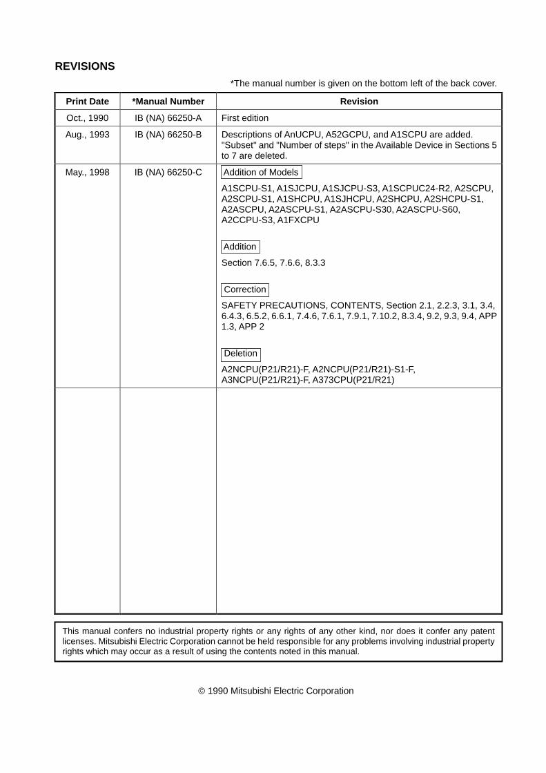
REVISIONS *The manual number is given on the bottom left of the back cover.
Print Date *Manual Number Revision
Oct., 1990 IB (NA) 66250-A First edition
Aug., 1993 IB (NA) 66250-B Descriptions of AnUCPU, A52GCPU, and A1SCPU are added. "Subset" and "Number of steps" in the Available Device in Sections 5 to 7 are deleted.
May., 1998 IB (NA) 66250-C Addition of Models
A1SCPU-S1, A1SJCPU, A1SJCPU-S3, A1SCPUC24-R2, A2SCPU, A2SCPU-S1, A1SHCPU, A1SJHCPU, A2SHCPU, A2SHCPU-S1, A2ASCPU, A2ASCPU-S1, A2ASCPU-S30, A2ASCPU-S60, A2CCPU-S3, A1FXCPU
Addition
Section 7.6.5, 7.6.6, 8.3.3
Correction
SAFETY PRECAUTIONS, CONTENTS, Section 2.1, 2.2.3, 3.1, 3.4, 6.4.3, 6.5.2, 6.6.1, 7.4.6, 7.6.1, 7.9.1, 7.10.2, 8.3.4, 9.2, 9.3, 9.4, APP 1.3, APP 2
Deletion
A2NCPU(P21/R21)-F, A2NCPU(P21/R21)-S1-F, A3NCPU(P21/R21)-F, A373CPU(P21/R21)
� 1990 Mitsubishi Electric Corporation
This manual confers no industrial property rights or any rights of any other kind, nor does it confer any patent licenses. Mitsubishi Electric Corporation cannot be held responsible for any problems involving industrial propertyrights which may occur as a result of using the contents noted in this manual.

SAFETY CAUTIONS (You must read these cautions before using the product)
In connection with the use of this product, in addition to carefully reading both this manual and the related manuals indicated in this manual, it is also essential to pay due attention to safety and handle the product correctly. The safety cautions given here apply to this product in isolation. For information on the safety of the PC system as a whole, refer to the CPU module User's Manual. Store this manual carefully in a place where it is accessible for reference whenever necessary, and forward a copy of the manual to the end user.
− i −
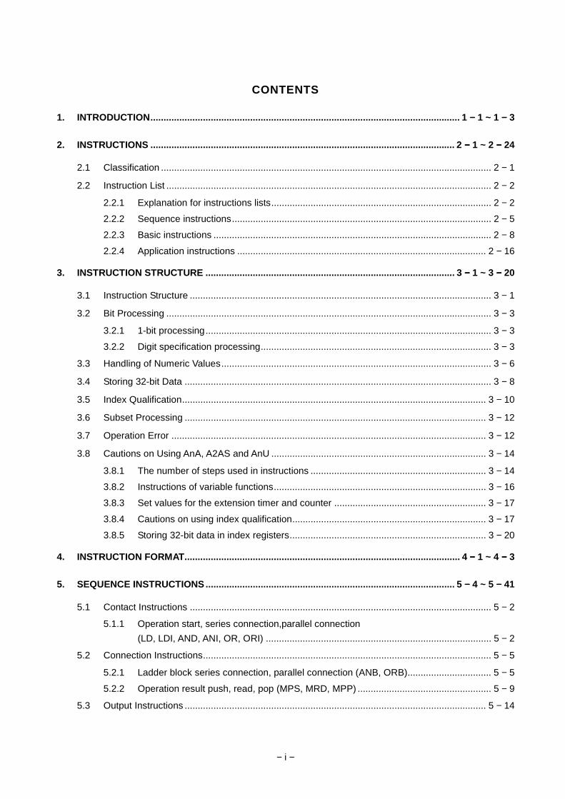
CONTENTS
1. INTRODUCTION...................................................................................................................... 1 −−−− 1 ~ 1 −−−− 3
2. INSTRUCTIONS .................................................................................................................... 2 −−−− 1 ~ 2 −−−− 24
2.1 Classification .............................................................................................................................. 2 − 1
2.2 Instruction List ............................................................................................................................ 2 − 2
2.2.1 Explanation for instructions lists.................................................................................... 2 − 2 2.2.2 Sequence instructions................................................................................................... 2 − 5 2.2.3 Basic instructions .......................................................................................................... 2 − 8
2.2.4 Application instructions ............................................................................................... 2 − 16
3. INSTRUCTION STRUCTURE ............................................................................................... 3 −−−− 1 ~ 3 −−−− 20
3.1 Instruction Structure ................................................................................................................... 3 − 1
3.2 Bit Processing ............................................................................................................................ 3 − 3
3.2.1 1-bit processing............................................................................................................. 3 − 3 3.2.2 Digit specification processing........................................................................................ 3 − 3
3.3 Handling of Numeric Values....................................................................................................... 3 − 6
3.4 Storing 32-bit Data ..................................................................................................................... 3 − 8
3.5 Index Qualification.................................................................................................................... 3 − 10
3.6 Subset Processing ................................................................................................................... 3 − 12
3.7 Operation Error ........................................................................................................................ 3 − 12
3.8 Cautions on Using AnA, A2AS and AnU .................................................................................. 3 − 14
3.8.1 The number of steps used in instructions ................................................................... 3 − 14 3.8.2 Instructions of variable functions................................................................................. 3 − 16 3.8.3 Set values for the extension timer and counter .......................................................... 3 − 17
3.8.4 Cautions on using index qualification.......................................................................... 3 − 17 3.8.5 Storing 32-bit data in index registers........................................................................... 3 − 20
4. INSTRUCTION FORMAT......................................................................................................... 4 −−−− 1 ~ 4 −−−− 3
5. SEQUENCE INSTRUCTIONS ............................................................................................... 5 −−−− 4 ~ 5 −−−− 41
5.1 Contact Instructions ................................................................................................................... 5 − 2
5.1.1 Operation start, series connection,parallel connection (LD, LDI, AND, ANI, OR, ORI) ...................................................................................... 5 − 2
5.2 Connection Instructions.............................................................................................................. 5 − 5
5.2.1 Ladder block series connection, parallel connection (ANB, ORB)................................ 5 − 5
5.2.2 Operation result push, read, pop (MPS, MRD, MPP) ................................................... 5 − 9
5.3 Output Instructions ................................................................................................................... 5 − 14
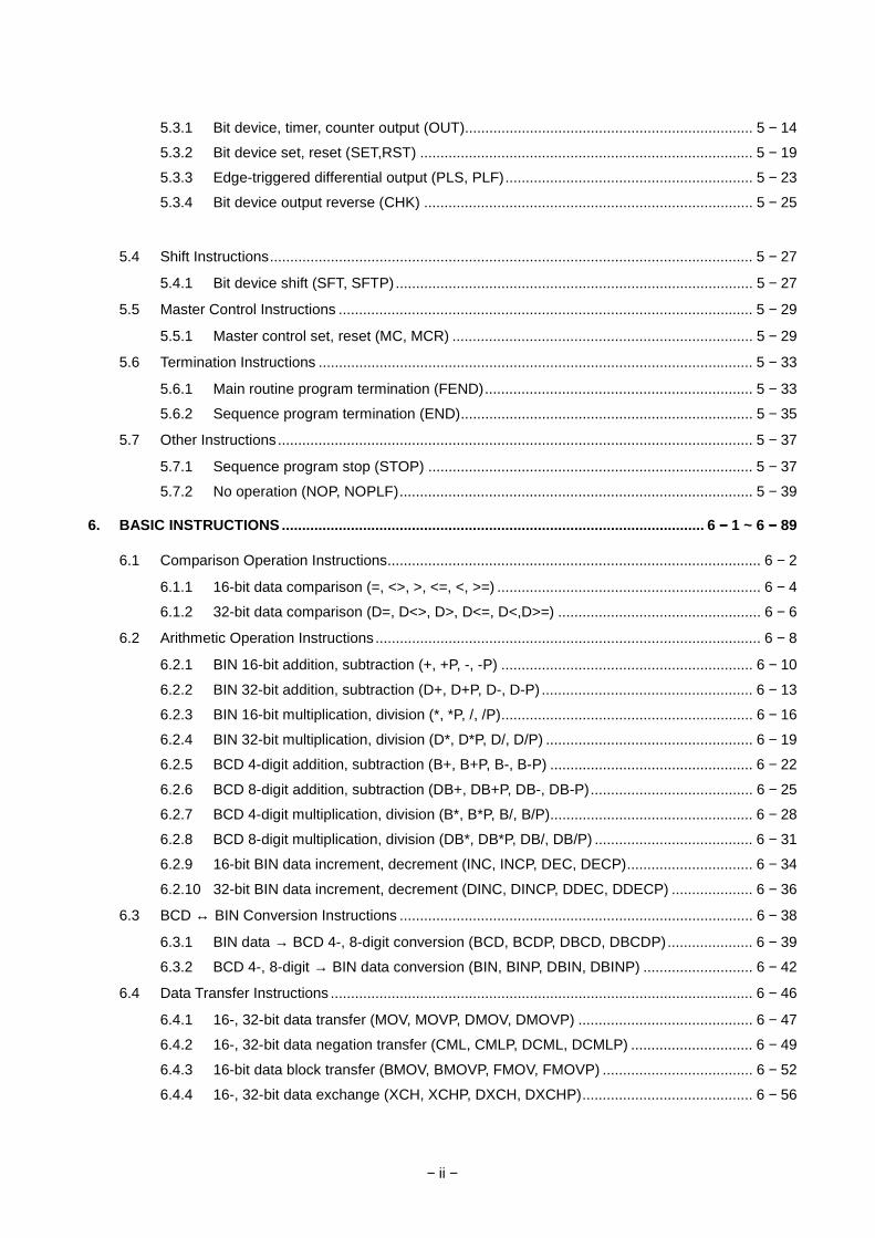
− ii −
5.3.1 Bit device, timer, counter output (OUT)....................................................................... 5 − 14 5.3.2 Bit device set, reset (SET,RST) .................................................................................. 5 − 19 5.3.3 Edge-triggered differential output (PLS, PLF)............................................................. 5 − 23 5.3.4 Bit device output reverse (CHK) ................................................................................. 5 − 25
5.4 Shift Instructions....................................................................................................................... 5 − 27
5.4.1 Bit device shift (SFT, SFTP)........................................................................................ 5 − 27
5.5 Master Control Instructions ...................................................................................................... 5 − 29
5.5.1 Master control set, reset (MC, MCR) .......................................................................... 5 − 29
5.6 Termination Instructions ........................................................................................................... 5 − 33
5.6.1 Main routine program termination (FEND).................................................................. 5 − 33 5.6.2 Sequence program termination (END)........................................................................ 5 − 35
5.7 Other Instructions..................................................................................................................... 5 − 37
5.7.1 Sequence program stop (STOP) ................................................................................ 5 − 37 5.7.2 No operation (NOP, NOPLF)....................................................................................... 5 − 39
6. BASIC INSTRUCTIONS ........................................................................................................ 6 −−−− 1 ~ 6 −−−− 89
6.1 Comparison Operation Instructions............................................................................................ 6 − 2
6.1.1 16-bit data comparison (=, <>, >, <=, <, >=) ................................................................. 6 − 4 6.1.2 32-bit data comparison (D=, D<>, D>, D<=, D<,D>=) .................................................. 6 − 6
6.2 Arithmetic Operation Instructions............................................................................................... 6 − 8
6.2.1 BIN 16-bit addition, subtraction (+, +P, -, -P) .............................................................. 6 − 10
6.2.2 BIN 32-bit addition, subtraction (D+, D+P, D-, D-P) .................................................... 6 − 13 6.2.3 BIN 16-bit multiplication, division (*, *P, /, /P).............................................................. 6 − 16 6.2.4 BIN 32-bit multiplication, division (D*, D*P, D/, D/P) ................................................... 6 − 19 6.2.5 BCD 4-digit addition, subtraction (B+, B+P, B-, B-P) .................................................. 6 − 22
6.2.6 BCD 8-digit addition, subtraction (DB+, DB+P, DB-, DB-P)........................................ 6 − 25 6.2.7 BCD 4-digit multiplication, division (B*, B*P, B/, B/P).................................................. 6 − 28 6.2.8 BCD 8-digit multiplication, division (DB*, DB*P, DB/, DB/P) ....................................... 6 − 31 6.2.9 16-bit BIN data increment, decrement (INC, INCP, DEC, DECP)............................... 6 − 34
6.2.10 32-bit BIN data increment, decrement (DINC, DINCP, DDEC, DDECP) .................... 6 − 36
6.3 BCD ↔ BIN Conversion Instructions ....................................................................................... 6 − 38
6.3.1 BIN data → BCD 4-, 8-digit conversion (BCD, BCDP, DBCD, DBCDP)..................... 6 − 39 6.3.2 BCD 4-, 8-digit → BIN data conversion (BIN, BINP, DBIN, DBINP) ........................... 6 − 42
6.4 Data Transfer Instructions ........................................................................................................ 6 − 46
6.4.1 16-, 32-bit data transfer (MOV, MOVP, DMOV, DMOVP) ........................................... 6 − 47 6.4.2 16-, 32-bit data negation transfer (CML, CMLP, DCML, DCMLP) .............................. 6 − 49
6.4.3 16-bit data block transfer (BMOV, BMOVP, FMOV, FMOVP) ..................................... 6 − 52 6.4.4 16-, 32-bit data exchange (XCH, XCHP, DXCH, DXCHP).......................................... 6 − 56

− iii −
6.5 Program Branch Instructions.................................................................................................... 6 − 58
6.5.1 Conditional jump, unconditional jump (CJ, SCJ, JMP) ............................................... 6 − 58 6.5.2 Subroutine call, return (CALL, CALLP, RET) .............................................................. 6 − 62
6.5.3 Interrupt enable, disable, return (EI, DI, IRET) ........................................................... 6 − 64 6.5.4 Microcomputer program call (SUB, SUBP)................................................................. 6 − 67
6.6 Program Switching Instructions................................................................................................ 6 − 69
6.6.1 Main ↔ subprogram switching (CHG) ........................................................................ 6 − 69
6.7 Link Refresh Instructions.......................................................................................................... 6 − 82
6.7.1 Link refresh (COM)...................................................................................................... 6 − 82
6.7.2 Link refresh enable, disable (EI, DI)............................................................................ 6 − 84 6.7.3 Partial refresh (SEG)................................................................................................... 6 − 87
7. APPLICATION INSTRUCTIONS ......................................................................................... 7 −−−− 1 ~ 7 −−−− 133
7.1 Logical Operation Instructions.................................................................................................... 7 − 2
7.1.1 16-, 32-bit data logical product (WAND, WANDP, DAND, DANDP) ............................. 7 − 3 7.1.2 16-, 32-bit data logical add (WOR, WORP, DOR, DORP) ............................................ 7 − 7
7.1.3 16-, 32-bit data exclusive logical add (WXOR, WXORP, DXOR, DXORP)..................7 − 11 7.1.4 16, 32-bit data NOT exclusive logical add (WXNR, WXNRP, DXNR, DXNRP) .......... 7 − 15 7.1.5 BIN 16-bit data 2’s complement (NEG, NEGP)........................................................... 7 − 19
7.2 Rotation Instructions ................................................................................................................ 7 − 21
7.2.1 16-bit data right rotation (ROR, RORP, RCR, PCRP)................................................. 7 − 22
7.2.2 16-bit data left rotation (ROL, ROLR, RCL, RCLP)..................................................... 7 − 24 7.2.3 32-bit data right rotation (DROR, DRORP, DRCR, DRCRP) ...................................... 7 − 26 7.2.4 32-bit data left rotation (DROL, DROLP, DRCL, DRCLP)........................................... 7 − 28
7.3 Shift Instructions....................................................................................................................... 7 − 30
7.3.1 16-bit data n-bit right shift, left shift (SFR, SFRP, SFL, SFLP).................................... 7 − 31
7.3.2 n-bit data 1-bit right shift, left shift (BSFR, BSFRP, BSFL, BSFLP) ............................ 7 − 33 7.3.3 n-word data 1-word right shift, left shift (DSFR, DSFRP, DSFL, DSFLP) ................... 7 − 35
7.4 Data Processing Instructions ................................................................................................... 7 − 37
7.4.1 16-bit data search (SER, SERP)................................................................................. 7 − 38 7.4.2 16-, 32-bit data bit check (SUM, SUMP, DSUM, DSUMP).......................................... 7 − 40 7.4.3 8 ↔ 256-bit decode, encode (DECO, DECOP, ENCO, ENCOP) ............................... 7 − 42
7.4.4 7 segment decode (SEG)............................................................................................ 7 − 44 7.4.5 Word device bit set, reset (BSET, BSETP, BRST, BRSTP) ........................................ 7 − 46 7.4.6 16-bit data dissociation, association (DIS, DISP, UNI, UNIP) ..................................... 7 − 48 7.4.7 ASCII code conversion (ASC)..................................................................................... 7 − 51
7.5 FIFO Instructions...................................................................................................................... 7 − 53
7.5.1 FIFO table write, read (FIFW, FIFWP, FIFR, FIFRP) .................................................. 7 − 54
7.6 Buffer Memory Access Instructions.......................................................................................... 7 − 58
− iv −
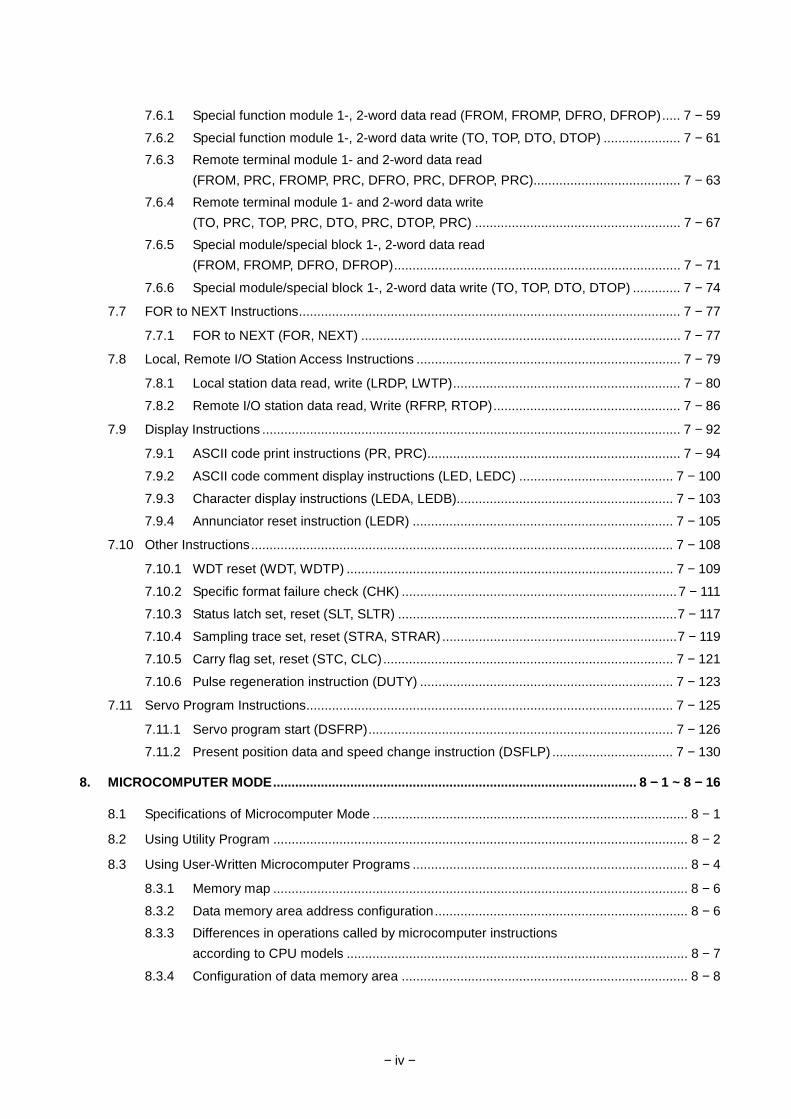
7.6.1 Special function module 1-, 2-word data read (FROM, FROMP, DFRO, DFROP)..... 7 − 59 7.6.2 Special function module 1-, 2-word data write (TO, TOP, DTO, DTOP) ..................... 7 − 61 7.6.3 Remote terminal module 1- and 2-word data read
(FROM, PRC, FROMP, PRC, DFRO, PRC, DFROP, PRC)........................................ 7 − 63 7.6.4 Remote terminal module 1- and 2-word data write
(TO, PRC, TOP, PRC, DTO, PRC, DTOP, PRC) ........................................................ 7 − 67 7.6.5 Special module/special block 1-, 2-word data read
(FROM, FROMP, DFRO, DFROP).............................................................................. 7 − 71
7.6.6 Special module/special block 1-, 2-word data write (TO, TOP, DTO, DTOP) ............. 7 − 74
7.7 FOR to NEXT Instructions........................................................................................................ 7 − 77
7.7.1 FOR to NEXT (FOR, NEXT) ....................................................................................... 7 − 77
7.8 Local, Remote I/O Station Access Instructions ........................................................................ 7 − 79
7.8.1 Local station data read, write (LRDP, LWTP).............................................................. 7 − 80 7.8.2 Remote I/O station data read, Write (RFRP, RTOP)................................................... 7 − 86
7.9 Display Instructions .................................................................................................................. 7 − 92
7.9.1 ASCII code print instructions (PR, PRC)..................................................................... 7 − 94
7.9.2 ASCII code comment display instructions (LED, LEDC) .......................................... 7 − 100 7.9.3 Character display instructions (LEDA, LEDB)........................................................... 7 − 103 7.9.4 Annunciator reset instruction (LEDR) ....................................................................... 7 − 105
7.10 Other Instructions................................................................................................................... 7 − 108
7.10.1 WDT reset (WDT, WDTP) ......................................................................................... 7 − 109
7.10.2 Specific format failure check (CHK) ...........................................................................7 − 111 7.10.3 Status latch set, reset (SLT, SLTR) ............................................................................7 − 117 7.10.4 Sampling trace set, reset (STRA, STRAR) ................................................................7 − 119 7.10.5 Carry flag set, reset (STC, CLC)............................................................................... 7 − 121
7.10.6 Pulse regeneration instruction (DUTY) ..................................................................... 7 − 123
7.11 Servo Program Instructions.................................................................................................... 7 − 125
7.11.1 Servo program start (DSFRP)................................................................................... 7 − 126 7.11.2 Present position data and speed change instruction (DSFLP) ................................. 7 − 130
8. MICROCOMPUTER MODE................................................................................................... 8 −−−− 1 ~ 8 −−−− 16
8.1 Specifications of Microcomputer Mode ...................................................................................... 8 − 1
8.2 Using Utility Program ................................................................................................................. 8 − 2
8.3 Using User-Written Microcomputer Programs ........................................................................... 8 − 4
8.3.1 Memory map ................................................................................................................. 8 − 6 8.3.2 Data memory area address configuration..................................................................... 8 − 6 8.3.3 Differences in operations called by microcomputer instructions
according to CPU models ............................................................................................. 8 − 7
8.3.4 Configuration of data memory area .............................................................................. 8 − 8

− v −
9. ERROR CODE LIST .............................................................................................................. 9 −−−− 1 ~ 9 −−−− 21
9.1 Reading Error Codes ................................................................................................................. 9 − 1
9.2 Error Code List for the CPUs of Other Than AnACPU, A2ASCPU and AnUCPU ..................... 9 − 1
9.3 Error Code List for the AnACPU ................................................................................................ 9 − 6
9.4 Error Code List for the AnUCPU and A2ASCPU...................................................................... 9 − 13
APPENDICES......................................................................................................................APP −−−− 1 ~ APP −−−− 81
APPENDIX 1 SPECIAL RELAYS AND SPECIAL REGISTERS .................................................... APP − 1
1.1 Special Relay M .................................................................................................................... APP − 1
1.2 Special Relays for Link........................................................................................................ APP − 10
1.3 Special Registers ................................................................................................................ APP − 13
1.4 Special Registers for Link.................................................................................................... APP − 28
APPENDIX 2 OPERATION PROCESSING TIME ....................................................................... APP − 34
2.1 Instruction Processing Time of Small Size, Compact CPUs............................................... APP − 36
2.2 Instruction Processing Time of CPUs ................................................................................. APP − 61
APPENDIX 3 ASCII CODE TABLE .............................................................................................. APP − 74
APPENDIX 4 FORMATS OF PROGRAM SHEETS .................................................................... APP − 75
1. INTRODUCTION
1 − 1
MELSEC-A
1. INTRODUCTION
This manual explains how to use the MELSEC-A series sequence control
instructions and microcomputer programs.
MELSEC-A series programmable controllers have a parameter which is used to
designate functions and device use ranges.
The functions and device use ranges are determined by the parameter values.
The parameters of CPU are set to default values. If the default can be used for the
purpose, it is not necessary to set the parameter.
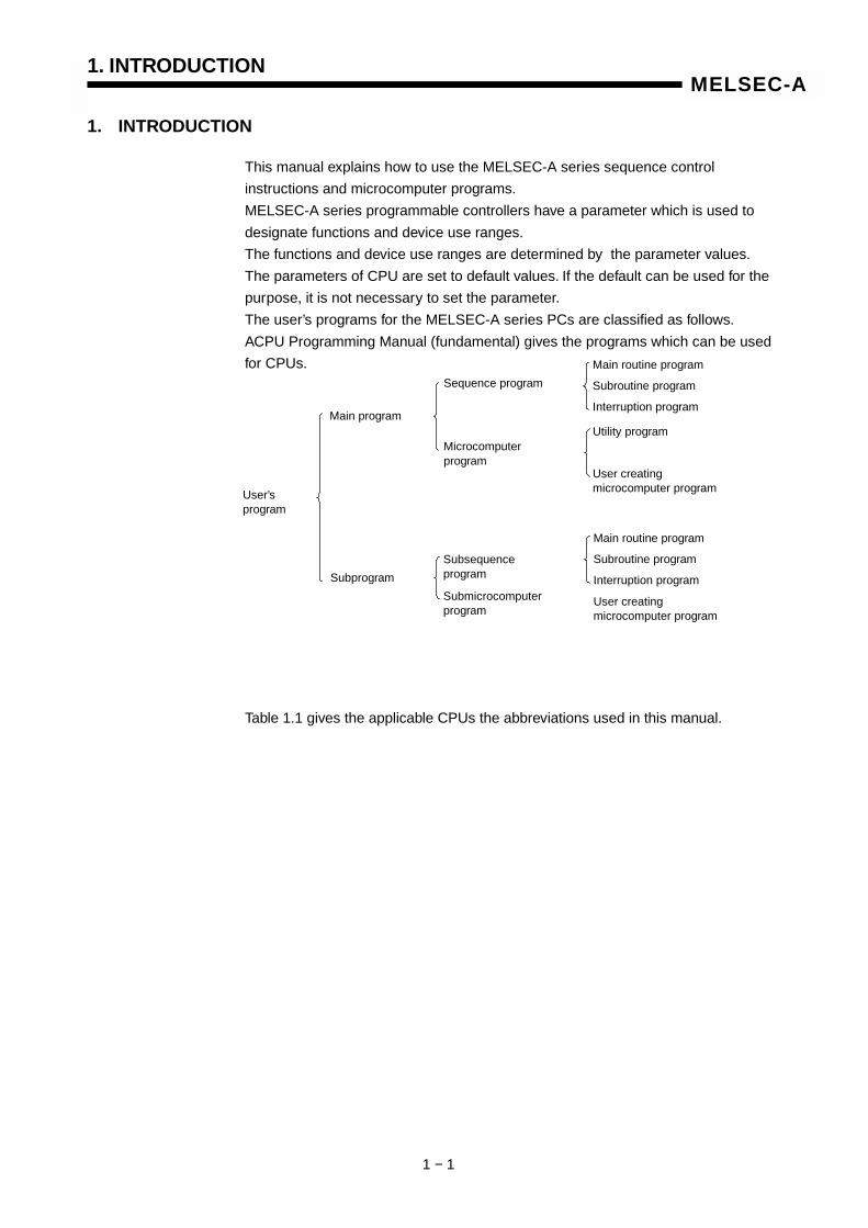
The user’s programs for the MELSEC-A series PCs are classified as follows.
ACPU Programming Manual (fundamental) gives the programs which can be used
for CPUs.
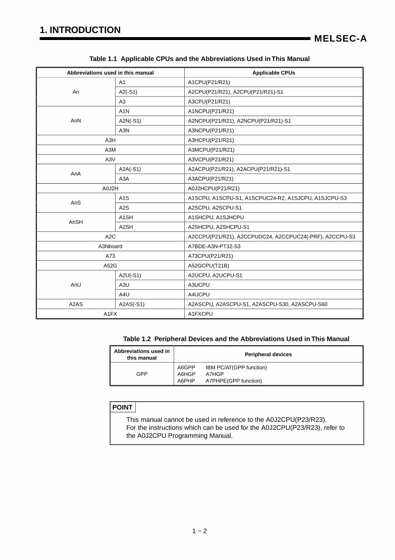
Table 1.1 gives the applicable CPUs the abbreviations used in this manual.
User’sprogram
Main routine program
Subroutine program
Interruption program
Utility program
User creatingmicrocomputer program
Main routine program
Subroutine program
Interruption program
User creatingmicrocomputer program
Subsequenceprogram
Submicrocomputerprogram
Sequence program
Microcomputerprogram
Main program
Subprogram
1. INTRODUCTION
1 − 2
MELSEC-A
Table 1.1 Applicable CPUs and the Abbreviations Used in This Manual
Abbreviations used in this manual Applicable CPUs
A1 A1CPU(P21/R21)
A2(-S1) A2CPU(P21/R21), A2CPU(P21/R21)-S1An
A3 A3CPU(P21/R21)
A1N A1NCPU(P21/R21)
A2N(-S1) A2NCPU(P21/R21), A2NCPU(P21/R21)-S1AnN
A3N A3NCPU(P21/R21)
A3H A3HCPU(P21/R21)
A3M A3MCPU(P21/R21)
A3V A3VCPU(P21/R21)
A2A(-S1) A2ACPU(P21/R21), A2ACPU(P21/R21)-S1AnA
A3A A3ACPU(P21/R21)
A0J2H A0J2HCPU(P21/R21)
A1S A1SCPU, A1SCPU-S1, A1SCPUC24-R2, A1SJCPU, A1SJCPU-S3AnS
A2S A2SCPU, A2SCPU-S1
A1SH A1SHCPU, A1SJHCPUAnSH
A2SH A2SHCPU, A2SHCPU-S1
A2C A2CCPU(P21/R21), A2CCPUDC24, A2CCPUC24(-PRF), A2CCPU-S3
A3Nboard A7BDE-A3N-PT32-S3
A73 A73CPU(P21/R21)
A52G A52GCPU(T21B)
A2U(-S1) A2UCPU, A2UCPU-S1
A3U A3UCPUAnU
A4U A4UCPU
A2AS A2AS(-S1) A2ASCPU, A2ASCPU-S1, A2ASCPU-S30, A2ASCPU-S60
A1FX A1FXCPU
Abbreviations used inthis manual
Peripheral devices
GPPA6GPP IBM PC/AT(GPP function)A6HGP A7HGPA6PHP A7PHPE(GPP function)
POINT
This manual cannot be used in reference to the A0J2CPU(P23/R23).For the instructions which can be used for the A0J2CPU(P23/R23), refer tothe A0J2CPU Programming Manual.
Table 1.2 Peripheral Devices and the Abbreviations Used in This Manual
1. INTRODUCTION
1 − 3
MELSEC-A
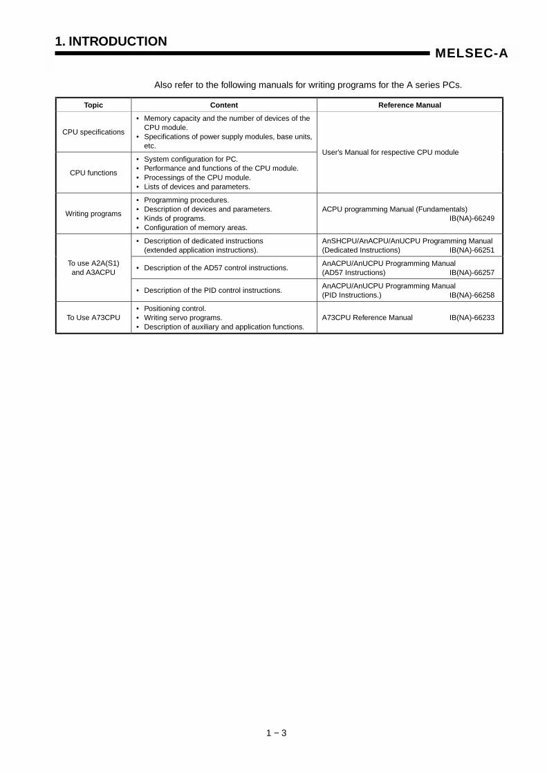
Also refer to the following manuals for writing programs for the A series PCs.
Topic Content Reference Manual
CPU specifications
• Memory capacity and the number of devices of theCPU module.
• Specifications of power supply modules, base units,etc.
CPU functions
• System configuration for PC.• Performance and functions of the CPU module.• Processings of the CPU module.• Lists of devices and parameters.
User’s Manual for respective CPU module
Writing programs
• Programming procedures.• Description of devices and parameters.• Kinds of programs.• Configuration of memory areas.
ACPU programming Manual (Fundamentals)IB(NA)-66249
• Description of dedicated instructions(extended application instructions).
AnSHCPU/AnACPU/AnUCPU Programming Manual(Dedicated Instructions) IB(NA)-66251
• Description of the AD57 control instructions.AnACPU/AnUCPU Programming Manual(AD57 Instructions) IB(NA)-66257
To use A2A(S1)and A3ACPU
• Description of the PID control instructions.AnACPU/AnUCPU Programming Manual(PID Instructions.) IB(NA)-66258
To Use A73CPU• Positioning control.• Writing servo programs.• Description of auxiliary and application functions.
A73CPU Reference Manual IB(NA)-66233
2. INSTRUCTIONS
2 − 1
MELSEC-A
2. INSTRUCTIONS
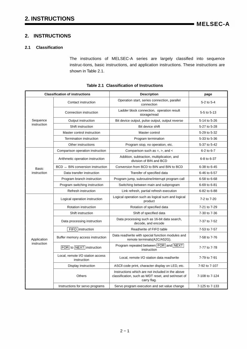
2.1 Classification
The instructions of MELSEC-A series are largely classified into sequence
instruc-tions, basic instructions, and application instructions. These instructions are
shown in Table 2.1.
Table 2.1 Classification of Instructions
Classification of instructions Description page
Contact instructionOperation start, series connection, parallel
connection5-2 to 5-4
Connection instructionLadder block connection, operation result
storage/read5-5 to 5-13
Output instruction Bit device output, pulse output, output reverse 5-14 to 5-26
Shift instruction Bit device shift 5-27 to 5-28
Master control instruction Master control 5-29 to 5-32
Termination instruction Program termination 5-33 to 5-36
Sequenceinstruction
Other instructions Program stop, no operation, etc. 5-37 to 5-42
Comparison operation instruction Comparison such as =, >, and < 6-2 to 6-7
Arithmetic operation instructionAddition, subtraction, multiplication, and
division of BIN and BCD6-8 to 6-37
BCD ↔ BIN conversion instruction Conversion from BCD to BIN and BIN to BCD 6-38 to 6-45
Data transfer instruction Transfer of specified data 6-46 to 6-57
Program branch instruction Program jump, subroutine/interrupt program call 6-58 to 6-68
Program switching instruction Switching between main and subprogram 6-69 to 6-81
Basicinstruction
Refresh instruction Link refresh, partial refresh execution 6-82 to 6-88
Logical operation instructionLogical operation such as logical sum and logical
product7-2 to 7-20
Rotation instruction Rotation of specified data 7-21 to 7-29
Shift instruction Shift of specified data 7-30 to 7-36
Data processing instructionData processing such as 16-bit data search,
decode, and encode7-37 to 7-52
FIFO instruction Read/write of FIFO table 7-53 to 7-57
Buffer memory access instructionData read/write with special function modules and
remote terminals(A2C/A52G).7-58 to 7-76
FOR to NEXT instructionProgram repeated between FOR and NEXT
instruction7-77 to 7-78
Local, remote I/O station accessinstruction
Local, remote I/O station data read/write 7-79 to 7-91
Display instruction ASCll code print, character display on LED, etc. 7-92 to 7-107
OthersInstructions which are not included in the above
classification, such as WDT reset, and set/reset ofcarry flag.
7-108 to 7-124
Applicationinstruction
Instructions for servo programs Servo program execution and set value change 7-125 to 7-133

2. INSTRUCTIONS
2 − 2
MELSEC-A
2.2 Instruction List
2.2.1 Explanation for instructions lists
Instruction lists in Section 2.2.2 to 2.2.4 are in the following format.
Table 2.2 Explanation for Instructions Lists
Classi-fication U
nit Instruction
SymbolSymbol Contents of Processing
Execu-tion
Con-dition
Nu
mb
ero
fst
eps
Ind
ex
Su
bse
t
Applicable CPU Page
+ 5 ○ 6-10
+P
(D)+(S)→(D)
5 ○ 6-10
+ 7 ○ 6-10
+P
(S1) + (S2) → (D)
7 ○ 6-10
- 5 ○ 6-10
-P
(D) - (S) → (D)
5 ○ 6-10
- 7 ○ 6-10
BIN16-bit
addition/subtrac
tion
16bi
ts
+P
(S1) - (S2) → (D)
7 ○ 6-10
Explanation
1)….. Classifies the instructions by applications.
2)….. Indicates the unit of processing at the execution of instruction.
Unit ofProcessing
Device Number of Points
X,Y,M,L,F,B Max. 16 points in units of 4 points.16 bits
T,C,D,W,R,A,Z,V 1 point
X,Y,M,L,F,B Max. 32 points In units of 4 points32 bits
T,C,D,W,R,A0,Z 2 Points
+P DS1 S2
*1
1) 2) 3) 4) 5) 6) 7) 8) 9) 10) 11)
+ DS
+P DS
+ DS1 S2
+P DS1 S2
- DS
- DS1 S2
- P S D
2. INSTRUCTIONS
2 − 3
MELSEC-A
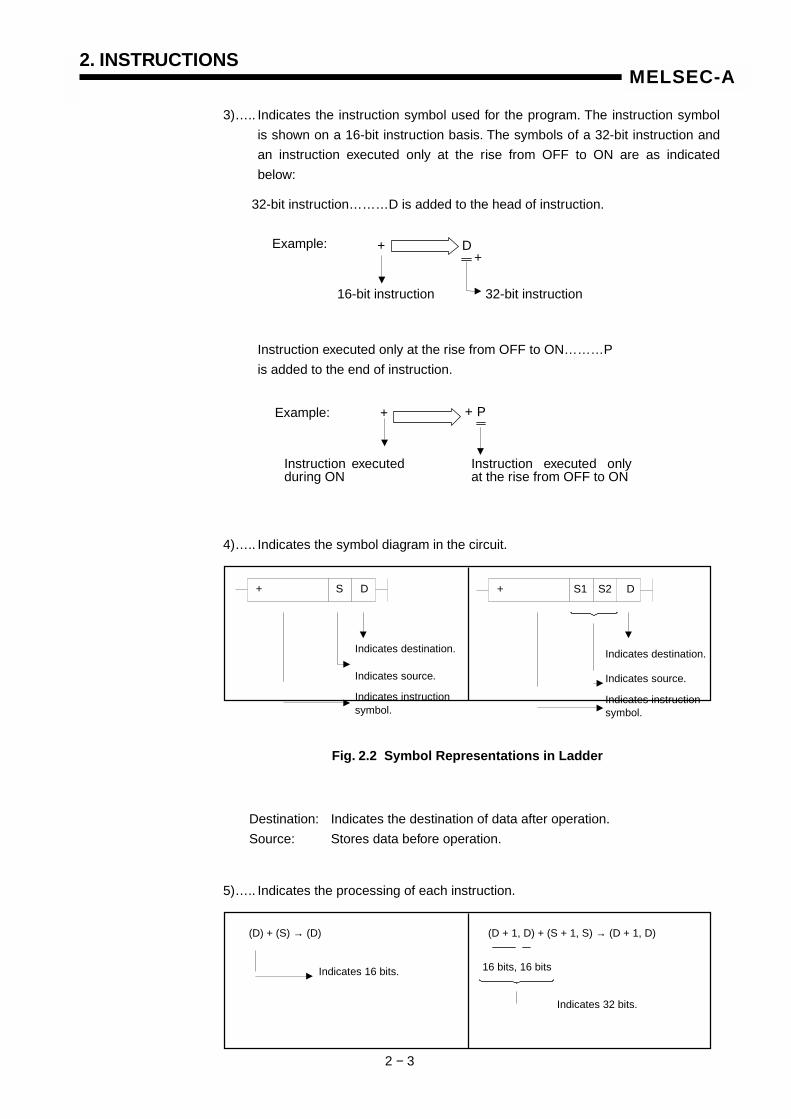
3)….. Indicates the instruction symbol used for the program. The instruction symbol
is shown on a 16-bit instruction basis. The symbols of a 32-bit instruction and
an instruction executed only at the rise from OFF to ON are as indicated
below:
Instruction executed only at the rise from OFF to ON………P
is added to the end of instruction.
4)….. Indicates the symbol diagram in the circuit.
Destination: Indicates the destination of data after operation.
Source: Stores data before operation.
5)….. Indicates the processing of each instruction.
32-bit instruction………D is added to the head of instruction.
+ D+
Example:
16-bit instruction 32-bit instruction
Example: + P+
Instruction executedduring ON
Instruction executed onlyat the rise from OFF to ON
+ DS
Indicates destination.
Indicates source.
Indicates instructionsymbol.
Indicates destination.
Indicates source.
Indicates instructionsymbol.
+ DS1 S2
Fig. 2.2 Symbol Representations in Ladder
(D) + (S) → (D)
Indicates 16 bits.
(D + 1, D) + (S + 1, S) → (D + 1, D)
16 bits, 16 bits
Indicates 32 bits.
2. INSTRUCTIONS
2 − 4
MELSEC-A
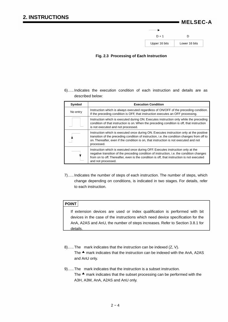
6)….. Indicates the execution condition of each instruction and details are as
described below:
Symbol Execution Condition
No entryInstruction which is always executed regardless of ON/OFF of the preceding condition.If the preceding condition is OFF, that instruction executes an OFF processing.
Instruction which is executed during ON. Executes instruction only while the precedingcondition of that instruction is on. When the preceding condition is off, that instructionis not executed and not processed.
Instruction which is executed once during ON. Executes instruction only at the positivetransition of the preceding condition of instruction, i.e. the condition changes from off toon. Thereafter, even if the condition is on, that instruction is not executed and notprocessed.
Instruction which is executed once during OFF. Executes instruction only at thenegative transition of the preceding condition of instruction, i.e. the condition changesfrom on to off. Thereafter, even is the condition is off, that instruction is not executedand not processed.
7)….. Indicates the number of steps of each instruction. The number of steps, which
change depending on conditions, is indicated in two stages. For details, refer
to each instruction.
POINT
If extension devices are used or index qualification is performed with bit
devices in the case of the instructions which need device specification for the
AnA, A2AS and AnU, the number of steps increases. Refer to Section 3.8.1 for
details.
8)….. The mark indicates that the instruction can be indexed (Z, V).
The mark indicates that the instruction can be indexed with the AnA, A2AS
and AnU only.
9)….. The mark indicates that the instruction is a subset instruction.
The mark indicates that the subset processing can be performed with the
A3H, A3M, AnA, A2AS and AnU only.
Upper 16 bits Lower 16 bits
D + 1 D
Fig. 2.3 Processing of Each Instruction

2. INSTRUCTIONS
2 − 5
MELSEC-A
10)… Indicates applicable CPU.
The ○ mark indicates that it is applicable to all types of CPUs.
The mark indicates that it is applicable to some types of CPUs.
The mark indicates that it is applicable to specific CPUs.
11)....Indicates a page which explains each instruction.
2. INSTRUCTIONS
2 − 13
MELSEC-A
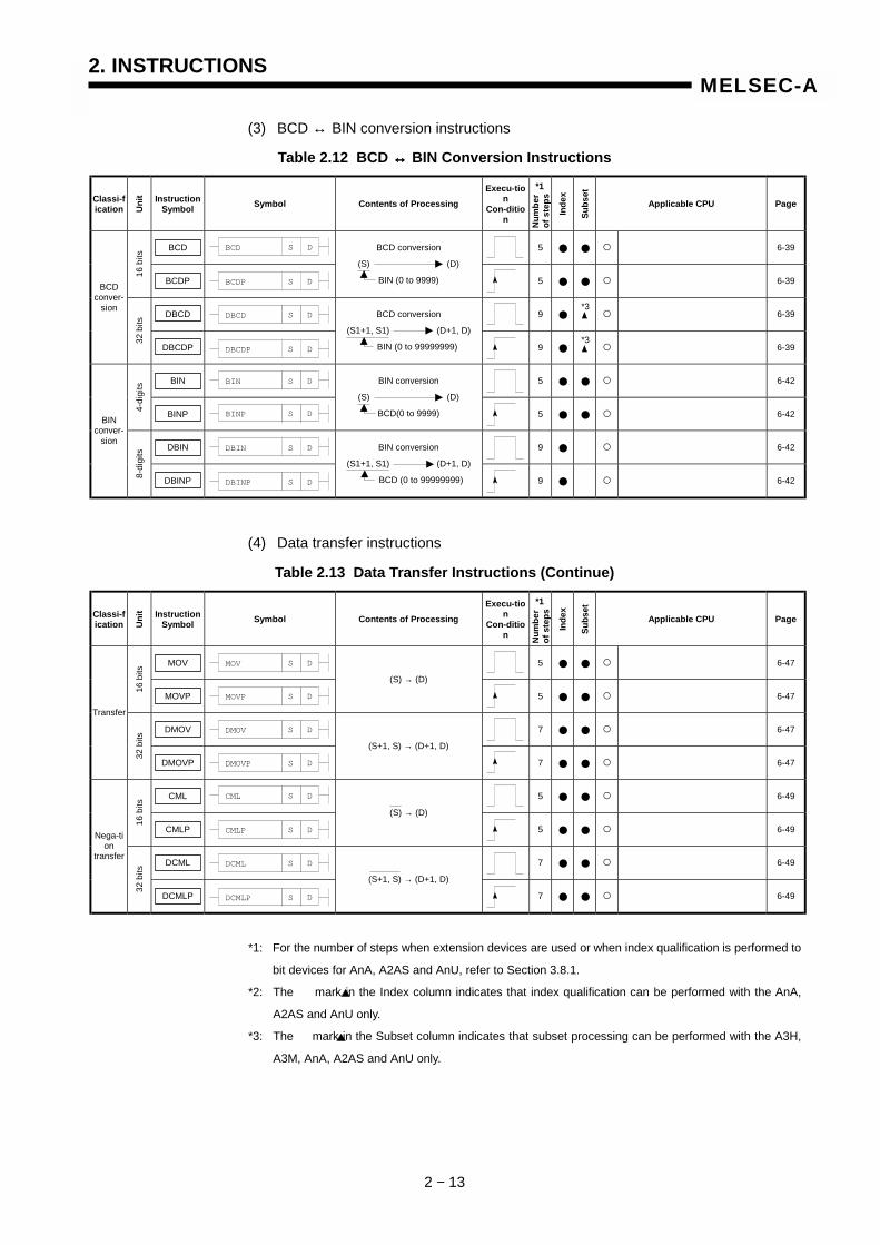
(3) BCD ↔ BIN conversion instructions
Table 2.12 BCD ↔↔↔↔ BIN Conversion Instructions
Classi-fication U
nit Instruction
Symbol Symbol Contents of Processing Execu-tio
n Con-ditio
n Num
ber
of s
teps
Inde
x
Subs
et
Applicable CPU Page
BCD
5 ● ● ○ 6-39
16 b
its
BCDP
BCD conversion
(S) (D)
BIN (0 to 9999)
5 ● ● ○ 6-39
DBCD
9 ● ○ 6-39
BCD conver-
sion
32 b
its
DBCDP
BCD conversion
(S1+1, S1) (D+1, D)
BIN (0 to 99999999)
9 ● ○ 6-39
BIN
5 ● ● ○ 6-42
4-di
gits
BINP
BIN conversion
(S) (D)
BCD(0 to 9999)
5 ● ● ○ 6-42
DBIN
9 ● ○ 6-42
BIN conver-
sion
8-di
gits
DBINP
BIN conversion
(S1+1, S1) (D+1, D)
BCD (0 to 99999999)
9 ● ○ 6-42
(4) Data transfer instructions
Table 2.13 Data Transfer Instructions (Continue)
Classi-fication U
nit Instruction
Symbol Symbol Contents of Processing Execu-tio
n Con-ditio
n Num
ber
of s
teps
Inde
x
Subs
et
Applicable CPU Page
MOV
5 ● ● ○ 6-47
16 b
its
MOVP
(S) → (D)
5 ● ● ○ 6-47
DMOV
7 ● ● ○ 6-47
Transfer
32 b
its
DMOVP
(S+1, S) → (D+1, D)
7 ● ● ○ 6-47
CML
5 ● ● ○ 6-49
16 b
its
CMLP
(S) → (D)
5 ● ● ○ 6-49
DCML
7 ● ● ○ 6-49
Nega-tion
transfer
32 b
its
DCMLP
(S+1, S) → (D+1, D)
7 ● ● ○ 6-49
*1: For the number of steps when extension devices are used or when index qualification is performed to
bit devices for AnA, A2AS and AnU, refer to Section 3.8.1.
*2: The mark in the Index column indicates that index qualification can be performed with the AnA,
A2AS and AnU only.
*3: The mark in the Subset column indicates that subset processing can be performed with the A3H,
A3M, AnA, A2AS and AnU only.
*1
*3
*3
BCD S D
BCDP S D
DBCD DS
DBCDP S D
BIN S D
BINP S D
DBIN S D
DBINP S D
*1
MOV S D
MOVP S D
DMOV S D
DMOVP S D
CML S D
CMLP S D
DCML S D
DCMLP S D

2. INSTRUCTIONS
2 − 14
MELSEC-A
Table 2.13 Data Transfer Instructions
Classi-fication U
nit Instruction
Symbol Symbol Contents of Processing Execu-tio
n Con-ditio
n Num
ber
of s
teps
Inde
x
Subs
et
Applicable CPU Page
BMOV
9 ● ○ 6-52
BMOVP
9 ● ○ 6-52
FMOV
9 ● ○ 6-52
Block transfer 16
bits
FMOVP
9 ● ○ 6-52
XCH
5 ● ● ○ 6-56
16 b
its
XCHP
(D1) ↔ (D2)
5 ● ● ○ 6-56
DXCH
7 ● ● ○ 6-56
Ex-change
32 b
its
DXCHP
(D1+1, D1) ↔ (D2+1, D2)
7 ● ● ○ 6-56
(5) Program branch instructions
Table 2.14 Program Branch Instructions
Classi-fication U
nit Instruction
Symbol Symbol Contents of Processing Execu-tio
n Con-ditio
n Num
ber
of s
teps
Inde
x
Subs
et
Applicable CPU Page
CJ Jumps to P** after the input condition is enabled.
3 ● ○ 6-58
SCJ Jumps to P ** beginning with the next scan after the input
condition is enabled.
3 ● ○ 6-58 Jump
JMP Unconditionally jumps to P**
3 ● ○ 6-58
CALL
3 ● ○ 6-62
CALLP
Executes the subroutine program at P** after the input
condition is enabled.
3 ● ○ Sub-rou
tine call
RET Returns execution from the
subroutine program to the sequence program.
1 ○ 6-62
EI Enables interrupt program run. Valid for AnN with M9053 off.
1 Not applicable to A3V, A2C and
A52G. 6-64
DI Disables interrupt program run. Valid for AnN with M9053 off.
1 Not applicable to A3V, A2C and
A52G. 6-64 Interrupt program
call
IRET Returns execution from the interrupt program to the sequence program.
1 Not applicable to A3V, A2C and
A52G. 6-64
SUB
3 ● Not applicable to AnA, A2AS and
AnU. 6-67 Micro-comput-e
r program
call
SUBP
Executes the microcomputer program specified by n.
3 ● Not applicable to AnA, A2AS and
AnU. 6-67
*1: For the number of step when extension devices are used or when index qualification is performed to
bit devices for AnA, A2AS and AnU, refer to Section 3.8.1.
*2: The mark in the Index column indicates that index qualification can be performed with the AnA,
A2AS and AnU only.
*3: The mark in the Subset column indicates that subset processing can be performed with the A3H, A3M, AnA, A2AS and AnU only
n
(S) (D)
n(S)
(D)
*1
*3
*3
*3
*3
BMOV nS D
BMOVP nS D
FMOV nS D
FMOVP nS D
XCH D1 D2
XCHP D1 D2
DXCH D1 D2
DXCHP D1 D2
*1
*3
*3
*3
*3
*3
CJ P**
SCJ P**
CALL P**
CALLP P**
EI
DI
IRET
SUB n
SUBP n
JMP P**
RET
2. INSTRUCTIONS
2 − 16
MELSEC-A
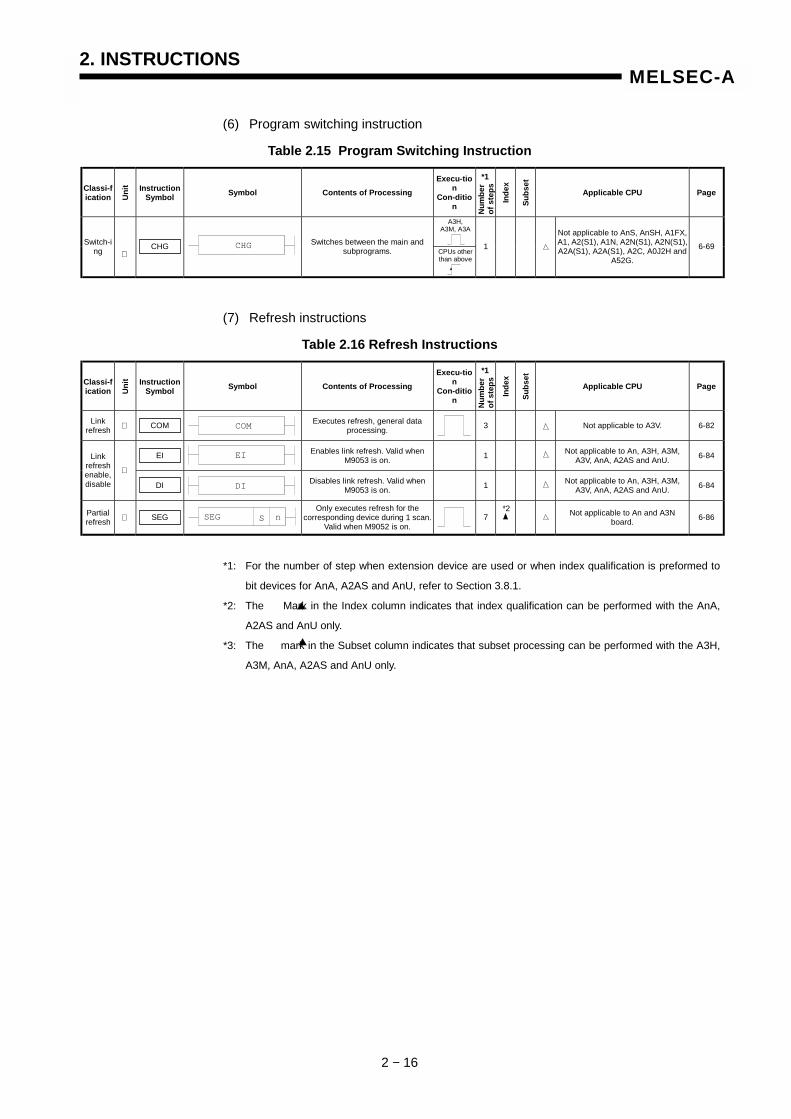
(6) Program switching instruction
Table 2.15 Program Switching Instruction
Classi-fication U
nit Instruction
Symbol Symbol Contents of Processing Execu-tio
n Con-ditio
n Num
ber
of s
teps
Inde
x
Subs
et
Applicable CPU Page
Switch-ing
CHG Switches between the main and subprograms.
1
Not applicable to AnS, AnSH, A1FX, A1, A2(S1), A1N, A2N(S1), A2N(S1), A2A(S1), A2A(S1), A2C, A0J2H and
A52G.
6-69
(7) Refresh instructions
Table 2.16 Refresh Instructions
Classi-fication U
nit Instruction
Symbol Symbol Contents of Processing Execu-tio
n Con-ditio
n Num
ber
of s
teps
Inde
x
Subs
et
Applicable CPU Page
Link refresh COM Executes refresh, general data
processing.
3 Not applicable to A3V. 6-82
EI Enables link refresh. Valid when M9053 is on.
1 Not applicable to An, A3H, A3M,
A3V, AnA, A2AS and AnU. 6-84 Link refresh enable, disable
DI Disables link refresh. Valid when M9053 is on.
1 Not applicable to An, A3H, A3M,
A3V, AnA, A2AS and AnU. 6-84
Partial refresh SEG
Only executes refresh for the corresponding device during 1 scan.
Valid when M9052 is on.
7 Not applicable to An and A3N
board. 6-86
*1: For the number of step when extension device are used or when index qualification is preformed to
bit devices for AnA, A2AS and AnU, refer to Section 3.8.1.
*2: The Mark in the Index column indicates that index qualification can be performed with the AnA,
A2AS and AnU only.
*3: The mark in the Subset column indicates that subset processing can be performed with the A3H,
A3M, AnA, A2AS and AnU only.
*1
A3H, A3M, A3A
CPUs other than above
CHG
*1
*2
COM
EI
DI
SEG nS

2. INSTRUCTIONS
2 − 19
MELSEC-A
(3) Shift instructions
Table 2.19 Shift Instructions
Classi-fication U
nit Instruction
Symbol Symbol Contents of Processing Execu-tio
n Con-ditio
n Num
ber
of s
teps
Inde
x
Subs
et
Applicable CPU Page
SFR
5 ● ● ○ 7-31
SFRP
5 ● ● ○ 7-31
SFL
5 ● ● ○ 7-31
n bit shift 16
bits
SFLP
5 ● ● ○ 7-31
BSFR
7 ● ○ 7-33
BSFRP
7 ● ○ 7-33
BSFL
7 ● ○ 7-33
1 bit shift n
bit
BSFLP
7 ● ○ 7-33
DSFR
7 ● Not applicable to A73 7-35
DSFRP
7 ● Not applicable to A73 7-35
DSFL
7 ● Not applicable to A73 7-35
1 ward shift n
war
d
DSFLP
7 ● Not applicable to A73 7-35
*1: For the number of steps when extension devices are used or when index qualification is performed to
bit devices for AnA, A2AS and AnU, refer to Section 3.8.1.
*2: The mark in the Index column indicates that qualification can be performed with the
AnA, A2AS and AnU only.
*3: The mark in the Subset column indicates that subset processing can be performed with the A3H,
A3M, AnA, A2AS and AnU only.
*1
*3
*3
*3
*3
0n15
0 to 0
0 Carry15to
BSFRP nD
BSFLP nD
DSFLP nD
DSFRP D n
SFR nD
SFL nD
BSFR nD
BSFL nD
DSFR nD
DSFL nD
Carry
15 n 0
0 to 0
15 0to
SFRP nD
SFLP nD
(D)
n
Carry
0
to
(D)
n
0
to
(D)
n
0
to
n
(D)
Carryto
0

2. INSTRUCTIONS
2 − 20
MELSEC-A
(1) Data processing instructions
Table 2.20 Date Processing Instructions
Classi-fication U
nit Instruction
Symbol Symbol Contents of Processing Execu-tio
n Con-ditio
n Num
ber
of s
teps
Inde
x
Subs
et
Applicable CPU Page
SER
9 ● ○ 7-38
Date search
SERP
9 ● ○ 7-38
SUM
3 ● ○ 7-40
16 b
its
SUMP
3 ● ○ 7-40
DSUM
3 ● ○ 7-40
Bit check
32 b
its
DSUMP
3 ● ○ 7-40
DECO
9 ● ○ 7-42
DECOP
9 ● ○ 7-42
ENCO
9 ● ○ 7-42
Decode Encode 2n
bits
ENCOP
9 ● ○ 7-42
7.seg-ment
decode SEG
7 ● Not applicable to A3V. 7-44
BSET
7 ● ○ 7-46
BSETP
7 ● ○ 7-46
BRST
7 ● ○ 7-46
Bit set reset
BRSTP
9 ● ○ 7-46
DIS
9 ● ○ 7-48
DISP
9 ● ○ 7-48
UNI
9 ● ○ 7-48
Accocia-tion
Dissoci-ation
16 b
its
UNIP
9 ● ○ 7-48
ASCII conver-
sion ASC
Converts alphanumeric characters into ASCII codes and stores into 4
points beginning with the devices, D.
13 ●
○ 7-51
*1: For the number of steps when extension devices are used or when index qualification is performed to
bit devices for AnA, A2AS and AnU, refer to Section 3.8.1.
*2: The mark in the Index column indicates that index qualification can be performed with the
AnA, A2AS and AnU only.
*3: The mark in the Subset column indicates that subset processing can be performed with the A3H,
A3M, AnA, A2AS and AnU only.
Decode from 256 to 8
2n bitsEncode(S)
(D)
n
Decode from 8 to 256(D)
(S)
n 2n bitsDecode
*3
*1
*3 A0 : Quantity of 1
015(S)
SUMP S
A0 : Quantity of 1
(S)(S+1)
DSUMP S
DECOP nDS
ENCOP nDS
SERP nS1 S2
SER nS1 S2
SUM S
DSUM S
DECO nDS
ENCO nDS
*3
15(D)
0n
1
15(D)
0n
0
4 bits
D4 bits
All 0
D+1D+2S
Whenn = 3
DISP nS D
4 bits
S
4 bits
S+1S+2
D
When n = 3UNIP nS D
ASC DAlphanumericcharacter
SEG nS
DIS nS D
UNI nS D
BSET D n
BSETP D n
BRST D n
BRSTP D n
A0 : Coinciding numberA1 : Coinciding quantity
(S2)
n(S1)
Valid for A N. DecodeA3H when M9052 is off.
7SEG(D)
n 0(S)
3 0
2. INSTRUCTIONS
2 − 21
MELSEC-A
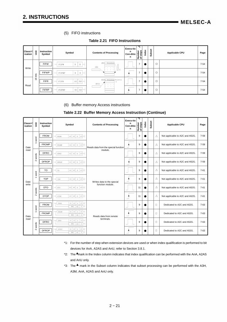
(5) FIFO instructions
Table 2.21 FIFO Instructions
Classi-fication U
nit Instruction
Symbol Symbol Contents of Processing Execu-tio
n Con-ditio
n Num
ber
of s
teps
Inde
x
Subs
et
Applicable CPU Page
FIFW
7 ● ○ 7-54
Write
FIFWP
7 ● ○ 7-54
FIFR
7 ● ○ 7-54
Read
16 b
its
FIFRP
7 ● ○ 7-54
(6) Buffer memory Access instructions
Table 2.22 Buffer Memory Access Instruction (Continue)
Classi-fication U
nit Instruction
Symbol Symbol Contents of Processing Execu-tio
n Con-ditio
n Num
ber
of s
teps
Inde
x
Subs
et
Applicable CPU Page
FROM
9 ● Not applicable to A2C and A52G. 7-59
1 w
ord
FROMP
9 ● Not applicable to A2C and A52G. 7-59
DFRO
9 ● Not applicable to A2C and A52G. 7-59
Date read
2 w
ords
DFROP
Reads data from the special function module.
9 ● Not applicable to A2C and A52G. 7-59
TO
9 ● Not applicable to A2C and A52G. 7-61
1 w
ord
TOP
9 ● Not applicable to A2C and A52G. 7-61
DTO
11 ● Not applicable to A2C and A52G. 7-61
Date write
2 w
ords
DTOP
Writes data to the special function module.
11 ● Not applicable to A2C and A52G. 7-61
FROM
9 ● Dedicated to A2C and A52G. 7-63
1 w
ord
FROMP
9 ● Dedicated to A2C and A52G. 7-63
DFRO
9 ● Dedicated to A2C and A52G. 7-63
Data read
2 w
ords
DFROP
Reads data from remote terminals.
9 ● Dedicated to A2C and A52G. 7-63
*1: For the number of step when extension devices are used or when index qualification is performed to bit
devices for AnA, A2AS and AnU, refer to Section 3.8.1.
*2: The mark in the Index column indicates that index qualification can be performed with the AnA, A2AS
and AnU only.
*3: The mark in the Subset column indicates that subset processing can be performed with the A3H,
A3M, AnA, A2AS and AnU only.
*1
*1
(S)
(D) Pointer
Pointer
+1
(D2) Pointer Pointer-1
(D1)
FIFW S D
FIFWP S D
FIFR D1 D2
FIFRP D1 D2
FROM n3n1 n2 D
FROMP n3n1 n2 D
DFRO n3n1 n2 D
DFROP n3n1 n2 D
TO n3n1 n2 S
TOP n3n1 n2 S
DTO n3n1 n2 S
DTOP n3n1 n2 D
FROM n3n1 n2 D
nPRC m1
FROMP n3n1 n2 D
nPRC m1
DFROP n3n1 n2 D
nPRC m1
DFRO n3n1 n2 D
nPRC m1
2. INSTRUCTIONS
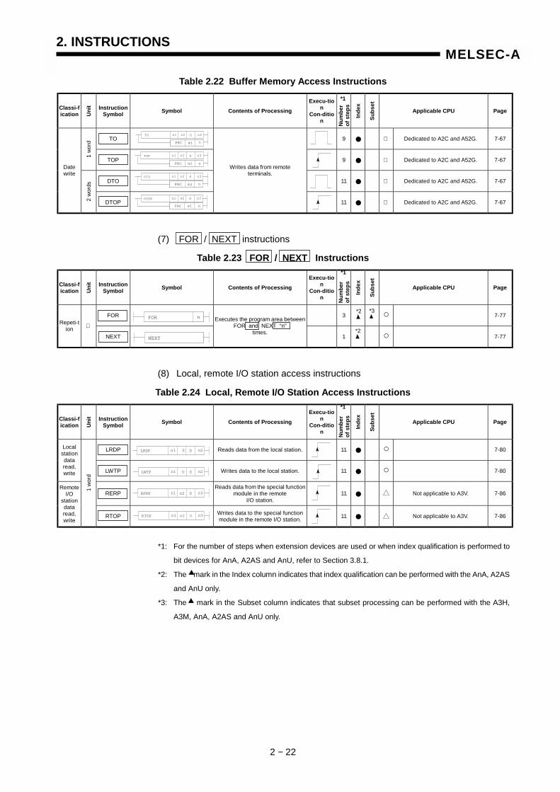
2 − 22
MELSEC-A
Table 2.22 Buffer Memory Access Instructions
Classi-fication U
nit Instruction
Symbol Symbol Contents of Processing Execu-tio
n Con-ditio
n Num
ber
of s
teps
Inde
x
Subs
et
Applicable CPU Page
TO
9 ● Dedicated to A2C and A52G. 7-67
1 w
ord
TOP
9 ● Dedicated to A2C and A52G. 7-67
DTO
11 ● Dedicated to A2C and A52G. 7-67
Date write
2 w
ords
DTOP
Writes data from remote terminals.
11 ● Dedicated to A2C and A52G. 7-67
(7) FOR / NEXT instructions
Table 2.23 FOR / NEXT Instructions
Classi-fication U
nit Instruction
Symbol Symbol Contents of Processing Execu-tio
n Con-ditio
n Num
ber
of s
teps
Inde
x
Subs
et
Applicable CPU Page
FOR
3 ○ 7-77
Repeti-tion
NEXT
Executes the program area between FOR and NEXT “n”
times. 1 ○ 7-77
(8) Local, remote I/O station access instructions
Table 2.24 Local, Remote I/O Station Access Instructions
Classi-fication U
nit Instruction
Symbol Symbol Contents of Processing Execu-tio
n Con-ditio
n Num
ber
of s
teps
Inde
x
Subs
et
Applicable CPU Page
LRDP
Reads data from the local station.
11 ● ○ 7-80 Local
station data read, write LWTP
Writes data to the local station.
11 ● ○ 7-80
RERP
Reads data from the special function module in the remote
I/O station.
11 ● Not applicable to A3V. 7-86
Remote I/O
station data read, write
1 w
ord
RTOP
Writes data to the special function module in the remote I/O station.
11 ● Not applicable to A3V. 7-86
*1: For the number of steps when extension devices are used or when index qualification is performed to
bit devices for AnA, A2AS and AnU, refer to Section 3.8.1.
*2: The mark in the Index column indicates that index qualification can be performed with the AnA, A2AS
and AnU only.
*3: The mark in the Subset column indicates that subset processing can be performed with the A3H,
A3M, AnA, A2AS and AnU only.
*2
*1
*2
*3
*1
FOR n
NEXT
LRDP n2n1 S D
LWTP n2n1 D S
RFRP n3n1 n2 D
RTOP n3n1 n2 D
TO n3n1 n2 S
nPRC m1
TOP n3n1 n2 S
nPRC m1
DTO n3n1 n2 S
nPRC m1
DTOP n3n1 n2 S
nPRC m1
*1
2. INSTRUCTIONS
2 − 23
MELSEC-A
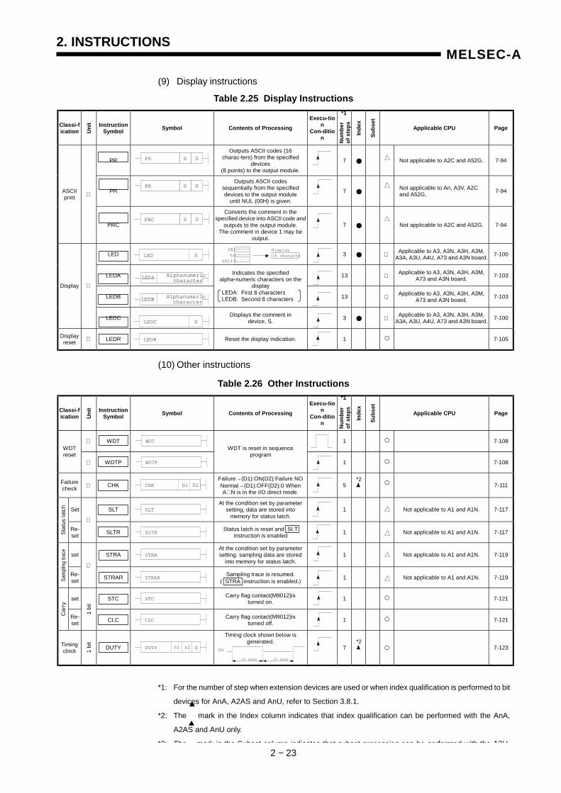
(9) Display instructions
Table 2.25 Display Instructions
Classi-fication U
nit Instruction
Symbol Symbol Contents of Processing Execu-tio
n Con-ditio
n Num
ber
of s
teps
Inde
x
Subs
et
Applicable CPU Page
PR
Outputs ASCII codes (16 charac-ters) from the specified
devices (8 points) to the output module.
7 ● Not applicable to A2C and A52G. 7-94
PR
Outputs ASCII codes sequentially from the specified devices to the output module
until NUL (00H) is given.
7 ● Not applicable to An, A3V, A2C
and A52G. 7-94 ASCII print
PRC
Converts the comment in the specified device into ASCII code and
outputs to the output module. The comment in device 1 may be
output.
7 ● Not applicable to A2C and A52G. 7-94
LED
3 ● Applicable to A3, A3N, A3H, A3M,
A3A, A3U, A4U, A73 and A3N board. 7-100
LEDA
13 Applicable to A3, A3N, A3H, A3M,
A73 and A3N board. 7-103
LEDB
Indicates the specified alpha-numeric characters on the
display LEDA: First 8 characters LEDB: Second 8 characters
13 Applicable to A3, A3N, A3H, A3M,
A73 and A3N board. 7-103
Display
LEDC
Displays the comment in
device, S.
3 ● Applicable to A3, A3N, A3H, A3M,
A3A, A3U, A4U, A73 and A3N board. 7-100
Display reset LEDR
Reset the display indication.
1 ○ 7-105
(10) Other instructions
Table 2.26 Other Instructions
Classi-fication U
nit Instruction
Symbol Symbol Contents of Processing Execu-tio
n Con-ditio
n Num
ber
of s
teps
Inde
x
Subs
et
Applicable CPU Page
WDT
1 ○ 7-108
WDT reset
WDTP
WDT is reset in sequence program
1 ○ 7-108
Failure check CHK
Failure→(D1):ON(D2):Failure NO Normal→(D1):OFF(D2):0 When A N is in the I/O direct mode.
5 ○ 7-111
Set SLT
At the condition set by parameter setting, data are stored into
memory for status latch.
1 Not applicable to A1 and A1N. 7-117
Stat
us la
tch
Re-set
SLTR
Status latch is reset and SI.T
instruction is enabled
1 Not applicable to A1 and A1N. 7-117
set STRA
At the condition set by parameter setting. sampling data are stored
into memory for status latch.
1 Not applicable to A1 and A1N. 7-119
Sam
pling
trac
e
Re-set
STRAR
Sampling trace is resumed.
( STRA instruction is enabled.)
1 Not applicable to A1 and A1N. 7-119
set STC
Carry flag contact(M9012)is
turned on.
1 ○ 7-121
Car
ry
Re-set
1 bi
t
CLC
Carry flag contact(M9012)is
turned off.
1 ○ 7-121
Timing clock 1
bit
DUTY
Timing clock shown below is generated.
7 ○ 7-123
*1
*2
PR S D
PRC S D
Display (S) to(S)+7
16 character
PR S D
LEDA Alphanumeric character
LEDB Alphanumeric character
CHK D1 D2
(D)
n1 scan n2 scan
*2
*1
*1: For the number of step when extension devices are used or when index qualification is performed to bit
devices for AnA, A2AS and AnU, refer to Section 3.8.1.
*2: The mark in the Index column indicates that index qualification can be performed with the AnA,
A2AS and AnU only.
*3: The mark in the Subset column indicates that subset processing can be performed with the A3H
LED S
LEDC S
LEDR
WDT
WDTP
SLT
SLTR
STRA
STRAR
STC
CLC
n1 n2 DDUTY
2. INSTRUCTIONS
2 − 24
MELSEC-A
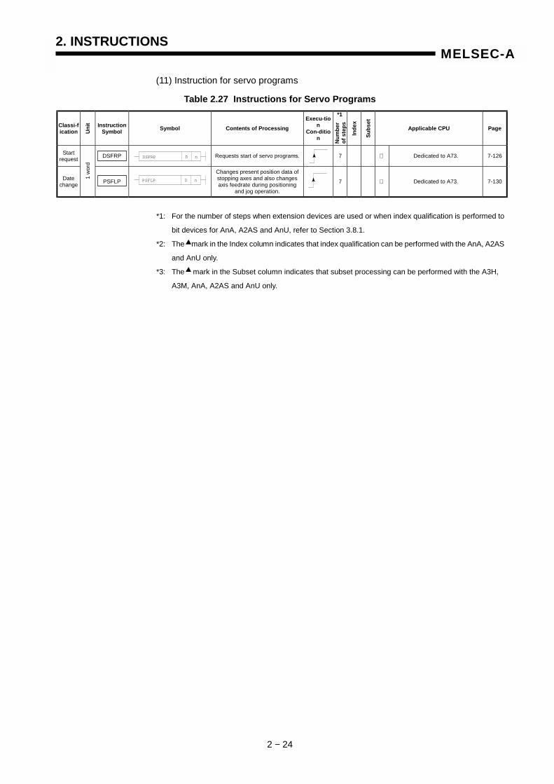
(11) Instruction for servo programs
Table 2.27 Instructions for Servo Programs
Classi-fication U
nit Instruction
Symbol Symbol Contents of Processing Execu-tio
n Con-ditio
n Num
ber
of s
teps
Inde
x
Subs
et
Applicable CPU Page
Start request DSFRP
Requests start of servo programs.
7 Dedicated to A73. 7-126
Date change
1 w
ord
PSFLP
Changes present position data of stopping axes and also changes axis feedrate during positioning
and jog operation.
7 Dedicated to A73. 7-130
*1: For the number of steps when extension devices are used or when index qualification is performed to
bit devices for AnA, A2AS and AnU, refer to Section 3.8.1.
*2: The mark in the Index column indicates that index qualification can be performed with the AnA, A2AS
and AnU only.
*3: The mark in the Subset column indicates that subset processing can be performed with the A3H,
A3M, AnA, A2AS and AnU only.
DSFRP D n
PSFLP D n
*1
2. INSTRUCTIONS
2 − 5
MELSEC-A
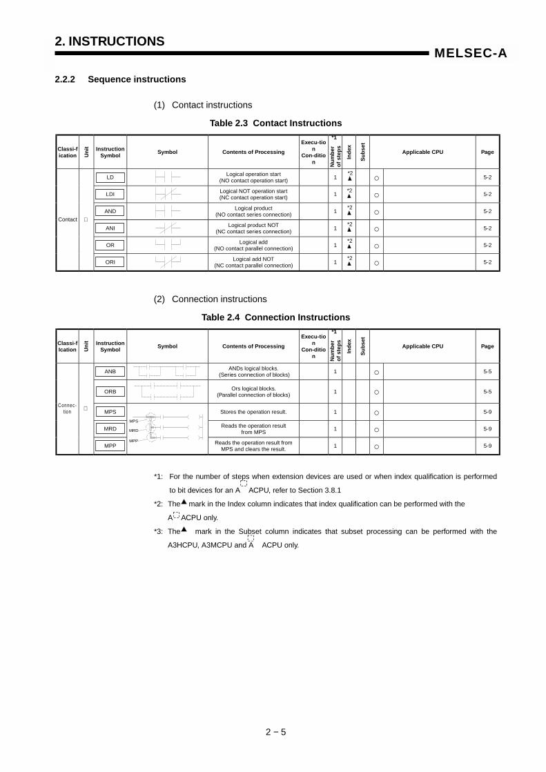
2.2.2 Sequence instructions
(1) Contact instructions
Table 2.3 Contact Instructions
Classi-fication U
nit Instruction
SymbolSymbol Contents of Processing
Execu-tion
Con-dition N
um
ber
of
step
s
Ind
ex
Su
bse
t
Applicable CPU Page
LD Logical operation start(NO contact operation start)
1 ○ 5-2
LDI Logical NOT operation start(NC contact operation start)
1 ○ 5-2
AND Logical product(NO contact series connection)
1 ○ 5-2
ANI Logical product NOT(NC contact series connection)
1 ○ 5-2
OR Logical add(NO contact parallel connection)
1 ○ 5-2
Contact
ORI Logical add NOT(NC contact parallel connection)
1 ○ 5-2
(2) Connection instructions
Table 2.4 Connection Instructions
Classi-fIcation U
nit Instruction
SymbolSymbol Contents of Processing
Execu-tion
Con-dition
Nu
mb
ero
fst
eps
Ind
ex
Su
bse
t
Applicable CPU Page
ANB ANDs logical blocks.(Series connection of blocks)
1 ○ 5-5
ORB Ors logical blocks.(Parallel connection of blocks)
1 ○ 5-5
MPS Stores the operation result. 1 ○ 5-9
MRD Reads the operation resultfrom MPS
1 ○ 5-9
C onnec-tion
MPP Reads the operation result fromMPS and clears the result.
1 ○ 5-9
*1: For the number of steps when extension devices are used or when index qualification is performed
to bit devices for an A ACPU, refer to Section 3.8.1
*2: The mark in the Index column indicates that index qualification can be performed with the
A ACPU only.
*3: The mark in the Subset column indicates that subset processing can be performed with the
A3HCPU, A3MCPU and A ACPU only.
MPS
MRD
MPP
*2
*2
*2
*2
*2
*2
*1
*1
2. INSTRUCTIONS
2 − 6
MELSEC-A
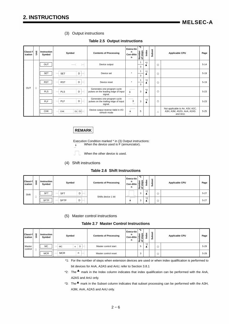
(3) Output instructions
Table 2.5 Output instructions
Classi-fication U
nit Instruction
SymbolSymbol Contents of Processing
Execu-tion
Con-dition N
um
ber
of
step
s
Ind
ex
Su
bse
t
Applicable CPU Page
1OUT Device output
3○ 5-14
1SET Device set *
3○ 5-19
1RST Device reset *
3○ 5-19
PLSGenerates one-program cycle
pulses on the leading edge of inputsignal.
3 ○ 5-23
PLFGenerates one-program cycle
pulses on the trailing edge of inputsignal.
3 ○ 5-23
OUT
CHK Device output reverse Valid in I/Orefresh mode
5 Not applicable to An, A3V, A2C,A3H, A3M, A52G, AnA, A2AS
and AnU.5-25
REMARK
Execution Condition marked * in (3) Output instructions:When the device used is F (annunciator).
When the other device is used.
(4) Shift instructions
Table 2.6 Shift Instructions
Classi-fication U
nit Instruction
SymbolSymbol Contents of Processing
Execu-tion
Con-dition N
um
ber
of
step
s
Ind
ex
Su
bse
t
Applicable CPU Page
SFT 3 ○ 5-27Shift
SFTP
Shifts device 1 bit
3 ○ 5-27
(5) Master control instructions
Table 2.7 Master Control Instructions
Classi-fication U
nit Instruction
SymbolSymbol Contents of Processing
Execu-tion
Con-dition
Nu
mb
ero
fst
eps
Ind
ex
Su
bse
t
Applicable CPU Page
MC Master control start 5 ○ 5-29Mastercontrol
MCR Master control reset 3 ○ 5-29
*1: For the number of steps when extension devices are used or when index qualification is performed to
bit devices for AnA, A2AS and AnU, refer to Section 3.8.1
*2: The mark in the Index column indicates that index qualification can be performed with the AnA,
A2AS and AnU only.
*3: The mark in the Subset column indicates that subset processing can be performed with the A3H,
A3M, AnA, A2AS and AnU only.
SET D
*2
*2
*2
*2
*2
*2
*2
RST D
PLS D
PLF D
CHK D1 D2
*1
*1
*2
SFT D
SFTP D
*1
MC n D
MCR n
2. INSTRUCTIONS
2 − 7
MELSEC-A
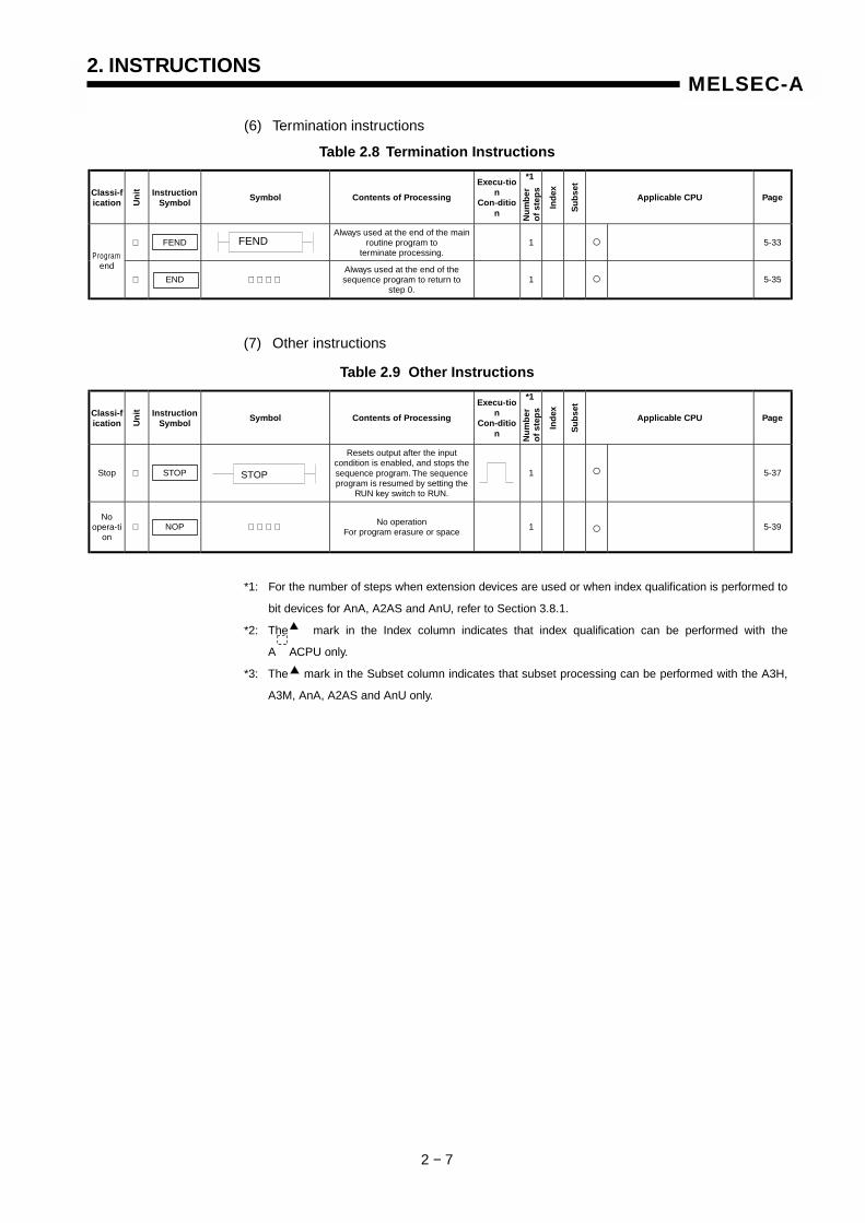
(6) Termination instructions
Table 2.8 Termination Instructions
Classi-fication U
nit Instruction
SymbolSymbol Contents of Processing
Execu-tion
Con-dition
Nu
mb
ero
fst
eps
Ind
ex
Su
bse
t
Applicable CPU Page
FENDAlways used at the end of the main
routine program toterminate processing.
1 ○ 5-33
Programend
END Always used at the end of thesequence program to return to
step 0.1 ○ 5-35
(7) Other instructions
Table 2.9 Other Instructions
Classi-fication U
nit Instruction
SymbolSymbol Contents of Processing
Execu-tion
Con-dition
Nu
mb
ero
fst
eps
Ind
ex
Su
bse
t
Applicable CPU Page
Stop STOP
Resets output after the inputcondition is enabled, and stops thesequence program. The sequenceprogram is resumed by setting the
RUN key switch to RUN.
1 ○ 5-37
Noopera-ti
on NOP No operation
For program erasure or space1 ○ 5-39
*1: For the number of steps when extension devices are used or when index qualification is performed to
bit devices for AnA, A2AS and AnU, refer to Section 3.8.1.
*2: The mark in the Index column indicates that index qualification can be performed with the
A ACPU only.
*3: The mark in the Subset column indicates that subset processing can be performed with the A3H,
A3M, AnA, A2AS and AnU only.
STOP
*1
*1
FEND
2. INSTRUCTIONS
2 − 8
MELSEC-A
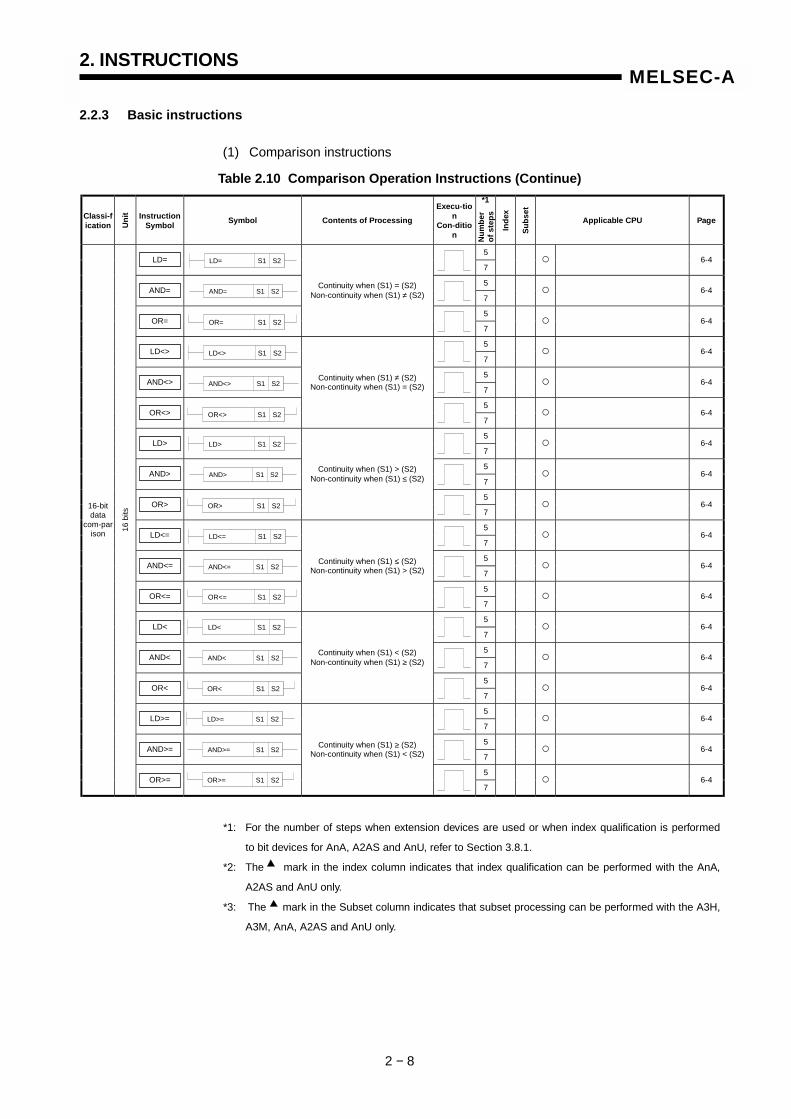
2.2.3 Basic instructions
(1) Comparison instructions
Table 2.10 Comparison Operation Instructions (Continue)
Classi-fication U
nit Instruction
SymbolSymbol Contents of Processing
Execu-tion
Con-dition N
um
ber
of
step
s
Ind
ex
Su
bse
t
Applicable CPU Page
5LD=
7○ 6-4
5AND=
7○ 6-4
5OR=
Continuity when (S1) = (S2)Non-continuity when (S1) ≠ (S2)
7○ 6-4
5LD<>
7○ 6-4
5AND<>
7○ 6-4
5OR<>
Continuity when (S1) ≠ (S2)Non-continuity when (S1) = (S2)
7○ 6-4
5LD>
7○ 6-4
5AND>
7○ 6-4
5OR>
Continuity when (S1) > (S2)Non-continuity when (S1) ≤ (S2)
7○ 6-4
5LD<=
7○ 6-4
5AND<=
7○ 6-4
5OR<=
Continuity when (S1) ≤ (S2)Non-continuity when (S1) > (S2)
7○ 6-4
5LD<
7○ 6-4
5AND<
7○ 6-4
5OR<
Continuity when (S1) < (S2)Non-continuity when (S1) ≥ (S2)
7○ 6-4
5LD>=
7○ 6-4
5AND>=
7○ 6-4
5
16-bitdata
com-parison
16bi
ts
OR>=
Continuity when (S1) ≥ (S2)Non-continuity when (S1) < (S2)
7○ 6-4
*1: For the number of steps when extension devices are used or when index qualification is performed
to bit devices for AnA, A2AS and AnU, refer to Section 3.8.1.
*2: The mark in the index column indicates that index qualification can be performed with the AnA,
A2AS and AnU only.
*3: The mark in the Subset column indicates that subset processing can be performed with the A3H,
A3M, AnA, A2AS and AnU only.
*1
LD= S1 S2
AND= S1 S2
OR= S1 S2
LD<> S1 S2
AND<> S1 S2
OR<> S1 S2
LD> S1 S2
AND> S1 S2
OR> S1 S2
LD<= S1 S2
AND<= S1 S2
OR<= S1 S2
LD< S1 S2
AND< S1 S2
OR< S1 S2
AND>= S1 S2
OR>= S1 S2
LD>= S1 S2

2. INSTRUCTIONS
2 − 9
MELSEC-A
Table 2.10 Comparison Operation Instructions
Classi-fication U
nit Instruction
SymbolSymbol Contents of Processing
Execu-tion
Con-dition
Nu
mb
ero
fst
eps
Ind
ex
Su
bse
t
Applicable CPU Page
LDD= 11 ○ 6-6
ANDD= 11 ○ 6-6
ORD=
Continuity when (S1+1, S1)= (S2+1, S2)
Non-continuity when (S1+1, S1)≠ (S2+1, S2)
11 ○ 6-6
LDD<> 11 ○ 6-6
ANDD<> 11 ○ 6-6
ORD<>
Continuity when (S1+1, S1)≠ (S2+1, S2)
Non-continuity when (S1+1, S1)= (S2+1, S2)
11 ○ 6-6
LDD> 11 ○ 6-6
ANDD> 11 ○ 6-6
ORD>
Continuity when (S1+1, S1)> (S2+1, S2)
Non-continuity when (S1+1, S1)≤ (S2+1, S2)
11 ○ 6-6
LDD<= 11 ○ 6-6
ANDD<= 11 ○ 6-6
ORD<=
Continuity when (S1+1, S1)≤ (S2+1, S2)
Non-continuity when (S1+1, S1)> (S2+1, S2)
11 ○ 6-6
LDD< 11 ○ 6-6
ANDD< 11 ○ 6-6
ORD<
Continuity when (S1+1, S1)< (S2+1, S2)
Non-continuity when (S1+1, S1)≥ (S2+1, S2)
11 ○ 6-6
LDD>= 11 ○ 6-6
ANDD>= 11 ○ 6-6
32 bitdata
com-parison
32bi
ts
ORD>=
Continuity when (S1+1, S1)≥ (S2+1, S2)
Non-continuity when (S1+1, S1)< (S2+1, S2)
11 ○ 6-6
*1: For the number of steps when extension devices are used or when index qualification is performed
to bit devices for AnA, A2AS and AnU, refer to Section 3.8.1.
*2: The mark in the Index column indicates that index qualification can be performed with the AnA,
A2AS and AnU only.
*3: The mark in the Subset column indicates that subset processing can be performed with the A3H,
A3M, AnA, A2AS and AnU only.
LDD= S1 S2
ANDD= S1 S2
ORD= S1 S2
LDD<> S1 S2
ANDD<> S1 S2
ORD<> S1 S2
LDD> S1 S2
ANDD> S1 S2
ORD> S1 S2
LDD<= S1 S2
ANDD<= S1 S2
ORD<= S1 S2
*1
LDD< S1 S2
ANDD< S1 S2
ORD< S1 S2
LDD>= S1 S2
ANDD>= S1 S2
ORD>= S1 S2
2. INSTRUCTIONS
2 − 16
MELSEC-A
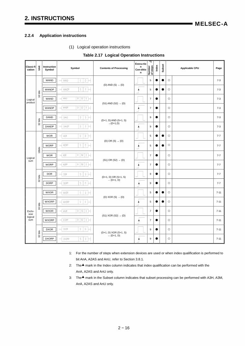
2.2.4 Application instructions
(1) Logical operation instructions
Table 2.17 Logical Operation Instructions
Classi-fication U
nit Instruction
Symbol Symbol Contents of Processing Execu-tio
n Con-ditio
n Num
ber
of s
teps
Inde
x
Subs
et
Applicable CPU Page
WAND
5 ● ● ○ 7-3
WANDP
(D) AND (S) → (D)
5 ● ● ○ 7-3
WAND
7 ● ○ 7-3
16 b
its
WANDP
(S1) AND (S2) → (D)
7 ● ○ 7-3
DAND
9 ● ○ 7-3
Logical product
32 b
its
DANDP
(D+1, D) AND (S+1, S) →(D+1,D)
9 ● ○ 7-3
WOR
5 ● ● ○ 7-7
WORP
(D) OR (S) → (D)
5 ● ● ○ 7-7
WOR
7 ● ○ 7-7
16bi
ts
WORP
(S1) OR (S2) → (D)
7 ● ○ 7-7
DOR
9 ● ○ 7-7
Logical sum
32 b
its
DORP
(D+1, D) OR (S+1, S) → (D+1, D)
9 ● ○ 7-7
WXOR
5 ● ● ○ 7-11
WXORP
(D) XOR (S) → (D)
5 ● ● ○ 7-11
WXOR
7 ● ○ 7-11
16 b
its
WXORP
(S1) XOR (S2) → (D)
7 ● ○ 7-11
DXOR
9 ● ○ 7-11
Exclu- sive
logical sum
32 b
its
DXORP
(D+1, D) XOR (S+1, S) → (D+1, D)
9 ● ○ 7-11
1: For the number of steps when extension devices are used or when index qualification is performed to
bit AnA, A2AS and AnU, refer to Section 3.8.1.
2: The mark in the Index column indicates that index qualification can be performed with the
AnA, A2AS and AnU only.
3: The mark in the Subset column indicates that subset processing can be performed with A3H, A3M,
AnA, A2AS and AnU only.
*1
2. INSTRUCTIONS
2 − 17
MELSEC-A
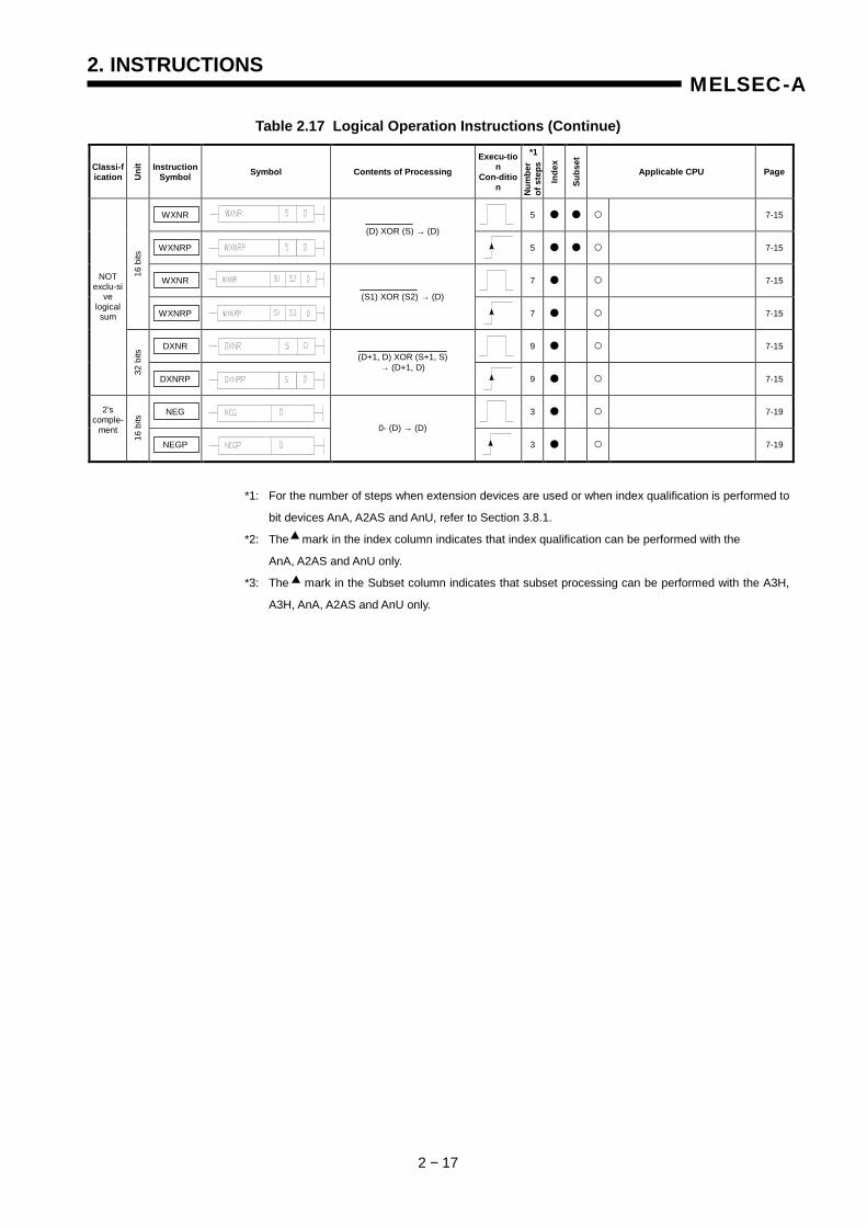
Table 2.17 Logical Operation Instructions (Continue)
Classi-fication U
nit Instruction
Symbol Symbol Contents of Processing Execu-tio
n Con-ditio
n Num
ber
of s
teps
Inde
x
Subs
et
Applicable CPU Page
WXNR
5 ● ● ○ 7-15
WXNRP
(D) XOR (S) → (D)
5 ● ● ○ 7-15
WXNR
7 ● ○ 7-15
16 b
its
WXNRP
(S1) XOR (S2) → (D)
7 ● ○ 7-15
DXNR
9 ● ○ 7-15
NOT exclu-si
ve logical sum
32 b
its
DXNRP
(D+1, D) XOR (S+1, S) → (D+1, D)
9 ● ○ 7-15
NEG
3 ● ○ 7-19 2’s
comple-ment
16 b
its
NEGP
0- (D) → (D)
3 ● ○ 7-19
*1: For the number of steps when extension devices are used or when index qualification is performed to
bit devices AnA, A2AS and AnU, refer to Section 3.8.1.
*2: The mark in the index column indicates that index qualification can be performed with the
AnA, A2AS and AnU only.
*3: The mark in the Subset column indicates that subset processing can be performed with the A3H,
A3H, AnA, A2AS and AnU only.
*1
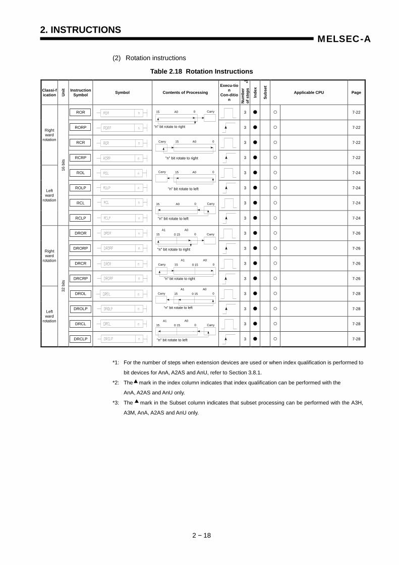
2. INSTRUCTIONS
2 − 18
MELSEC-A
015 Carry0 15A1 A0
"n" bit rotate to left
(2) Rotation instructions
Table 2.18 Rotation Instructions
Classi-fication U
nit Instruction
Symbol Symbol Contents of Processing Execu-tio
n Con-ditio
n Num
ber
of s
teps
Inde
x
Subs
et
Applicable CPU Page
ROR
3 ● ○ 7-22
RORP
3 ● ○ 7-22
RCR
3 ● ○ 7-22
Right ward
rotation
RCRP
3 ● ○ 7-22
ROL
3 ● ○ 7-24
ROLP
3 ● ○ 7-24
RCL
3 ● ○ 7-24
Left ward
rotation
16 b
its
RCLP
3 ● ○ 7-24
DROR
3 ● ○ 7-26
DRORP
3 ● ○ 7-26
DRCR
3 ● ○ 7-26
Right ward
rotation
DRCRP
3 ● ○ 7-26
DROL
3 ● ○ 7-28
DROLP
3 ● ○ 7-28
DRCL
3 ● ○ 7-28
Left ward
rotation
32 b
its
DRCLP
3 ● ○ 7-28
*1: For the number of steps when extension devices are used or when index qualification is performed to
bit devices for AnA, A2AS and AnU, refer to Section 3.8.1.
*2: The mark in the index column indicates that index qualification can be performed with the
AnA, A2AS and AnU only.
*3: The mark in the Subset column indicates that subset processing can be performed with the A3H,
A3M, AnA, A2AS and AnU only.
*1
"n" bit rotate to right
CarryA0 015
Carry A0 0 15
"n" bit rotate to right
Carry A0 0 15
"n" bit rotate to left
015 CarryA0
"n" bit rotate to left
015 Carry0 15A1 A0
"n" bit rotate to right
A1 A0 015Carry 0 15
"n" bit rotate to right
A1 A0 015Carry 0 15
"n" bit rotate to left
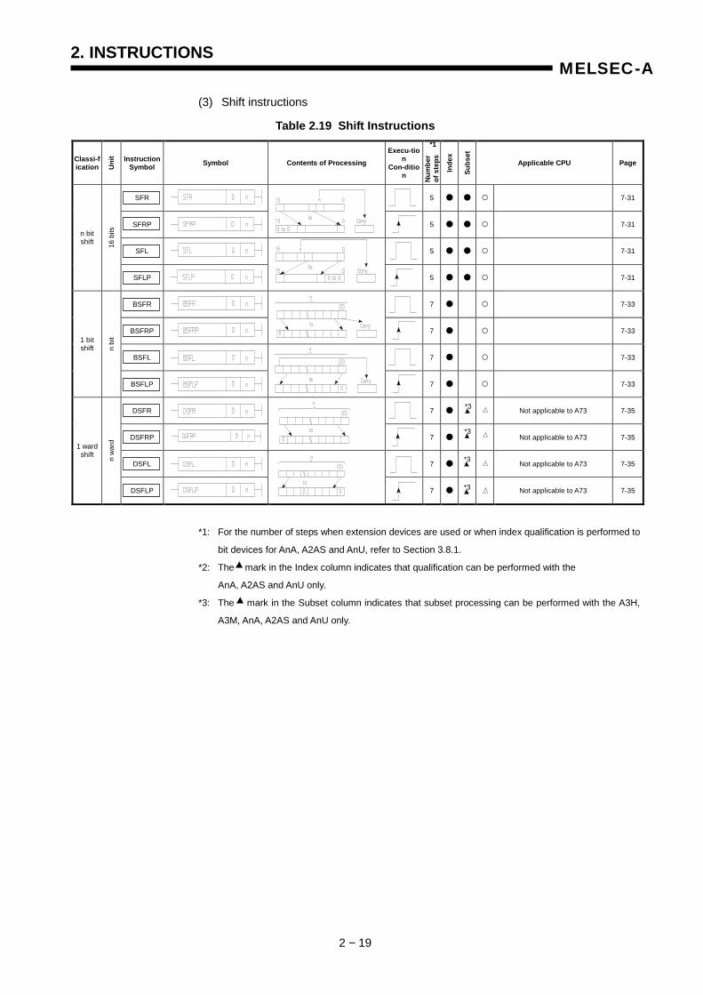
2. INSTRUCTIONS
2 − 19
MELSEC-A
(3) Shift instructions
Table 2.19 Shift Instructions
Classi-fication U
nit Instruction
Symbol Symbol Contents of Processing Execu-tio
n Con-ditio
n Num
ber
of s
teps
Inde
x
Subs
et
Applicable CPU Page
SFR
5 ● ● ○ 7-31
SFRP
5 ● ● ○ 7-31
SFL
5 ● ● ○ 7-31
n bit shift 16
bits
SFLP
5 ● ● ○ 7-31
BSFR
7 ● ○ 7-33
BSFRP
7 ● ○ 7-33
BSFL
7 ● ○ 7-33
1 bit shift n
bit
BSFLP
7 ● ○ 7-33
DSFR
7 ● Not applicable to A73 7-35
DSFRP
7 ● Not applicable to A73 7-35
DSFL
7 ● Not applicable to A73 7-35
1 ward shift n
war
d
DSFLP
7 ● Not applicable to A73 7-35
*1: For the number of steps when extension devices are used or when index qualification is performed to
bit devices for AnA, A2AS and AnU, refer to Section 3.8.1.
*2: The mark in the Index column indicates that qualification can be performed with the
AnA, A2AS and AnU only.
*3: The mark in the Subset column indicates that subset processing can be performed with the A3H,
A3M, AnA, A2AS and AnU only.
*1
*3
*3
*3
*3
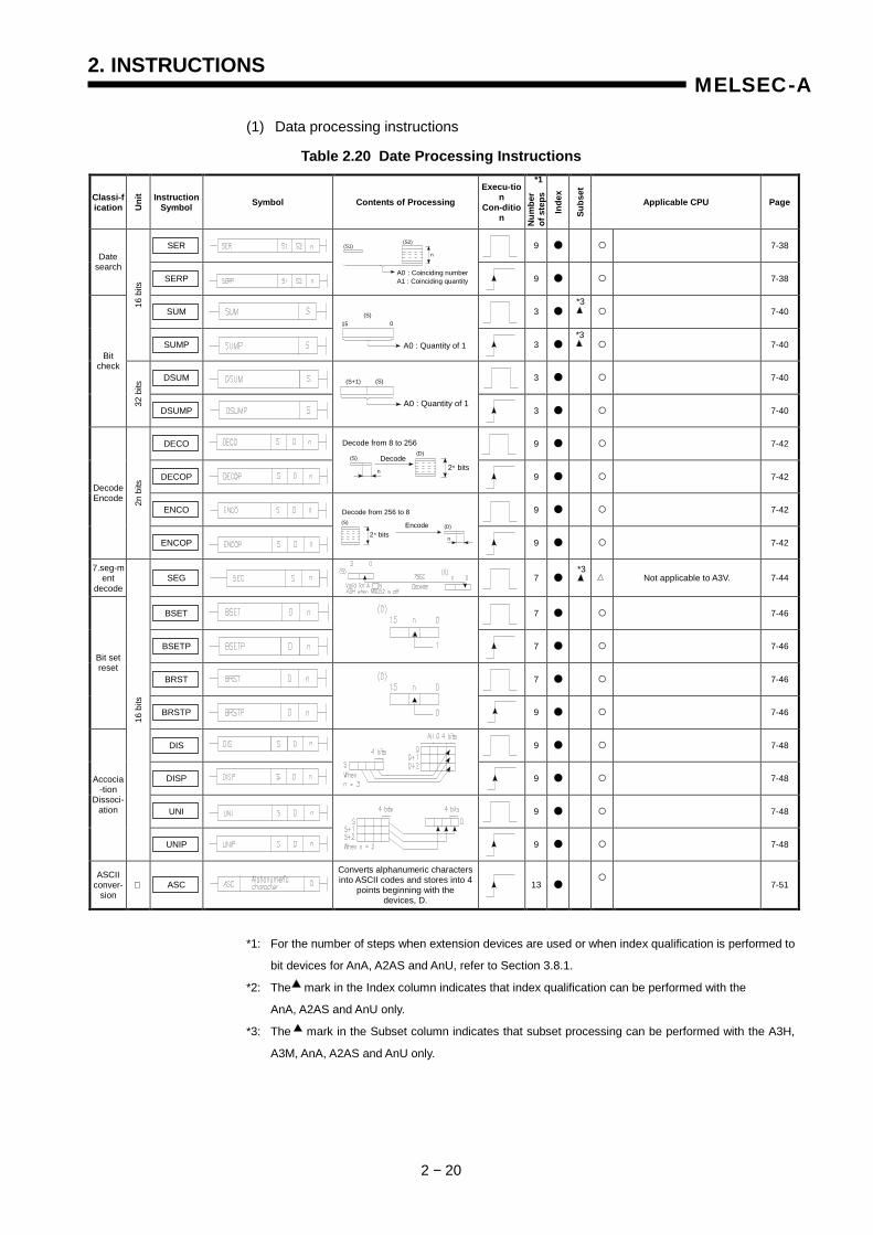
2. INSTRUCTIONS
2 − 20
MELSEC-A
(1) Data processing instructions
Table 2.20 Date Processing Instructions
Classi-fication U
nit Instruction
Symbol Symbol Contents of Processing Execu-tio
n Con-ditio
n Num
ber
of s
teps
Inde
x
Subs
et
Applicable CPU Page
SER
9 ● ○ 7-38
Date search
SERP
9 ● ○ 7-38
SUM
3 ● ○ 7-40
16 b
its
SUMP
3 ● ○ 7-40
DSUM
3 ● ○ 7-40
Bit check
32 b
its
DSUMP
3 ● ○ 7-40
DECO
9 ● ○ 7-42
DECOP
9 ● ○ 7-42
ENCO
9 ● ○ 7-42
Decode Encode 2n
bits
ENCOP
9 ● ○ 7-42
7.seg-ment
decode SEG
7 ● Not applicable to A3V. 7-44
BSET
7 ● ○ 7-46
BSETP
7 ● ○ 7-46
BRST
7 ● ○ 7-46
Bit set reset
BRSTP
9 ● ○ 7-46
DIS
9 ● ○ 7-48
DISP
9 ● ○ 7-48
UNI
9 ● ○ 7-48
Accocia-tion
Dissoci-ation
16 b
its
UNIP
9 ● ○ 7-48
ASCII conver-
sion ASC
Converts alphanumeric characters into ASCII codes and stores into 4
points beginning with the devices, D.
13 ●
○ 7-51
*1: For the number of steps when extension devices are used or when index qualification is performed to
bit devices for AnA, A2AS and AnU, refer to Section 3.8.1.
*2: The mark in the Index column indicates that index qualification can be performed with the
AnA, A2AS and AnU only.
*3: The mark in the Subset column indicates that subset processing can be performed with the A3H,
A3M, AnA, A2AS and AnU only.
Decode from 256 to 8
2n bitsEncode(S)
(D)
n
Decode from 8 to 256(D)
(S)
n 2n bitsDecode
*3
*1
*3A0 : Quantity of 1
015(S)
A0 : Quantity of 1
(S)(S+1)
*3
A0 : Coinciding numberA1 : Coinciding quantity
(S2)
n(S1)
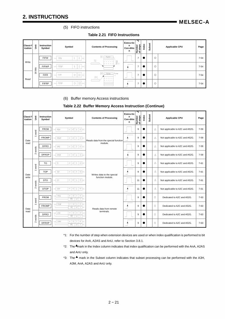
2. INSTRUCTIONS
2 − 21
MELSEC-A(5) FIFO instructions
Table 2.21 FIFO Instructions
Classi-fication U
nit Instruction
Symbol Symbol Contents of Processing Execu-tio
n Con-ditio
n Num
ber
of s
teps
Inde
x
Subs
et
Applicable CPU Page
FIFW
7 ● ○ 7-54
Write
FIFWP
7 ● ○ 7-54
FIFR
7 ● ○ 7-54
Read
16 b
its
FIFRP
7 ● ○ 7-54
(6) Buffer memory Access instructions
Table 2.22 Buffer Memory Access Instruction (Continue)
Classi-fication U
nit Instruction
Symbol Symbol Contents of Processing Execu-tio
n Con-ditio
n Num
ber
of s
teps
Inde
x
Subs
et
Applicable CPU Page
FROM
9 ● Not applicable to A2C and A52G. 7-59
1 w
ord
FROMP
9 ● Not applicable to A2C and A52G. 7-59
DFRO
9 ● Not applicable to A2C and A52G. 7-59
Date read
2 w
ords
DFROP
Reads data from the special function module.
9 ● Not applicable to A2C and A52G. 7-59
TO
9 ● Not applicable to A2C and A52G. 7-61
1 w
ord
TOP
9 ● Not applicable to A2C and A52G. 7-61
DTO
11 ● Not applicable to A2C and A52G. 7-61
Date write
2 w
ords
DTOP
Writes data to the special function module.
11 ● Not applicable to A2C and A52G. 7-61
FROM
9 ● Dedicated to A2C and A52G. 7-63
1 w
ord
FROMP
9 ● Dedicated to A2C and A52G. 7-63
DFRO
9 ● Dedicated to A2C and A52G. 7-63
Data read
2 w
ords
DFROP
Reads data from remote terminals.
9 ● Dedicated to A2C and A52G. 7-63
*1: For the number of step when extension devices are used or when index qualification is performed to bit
devices for AnA, A2AS and AnU, refer to Section 3.8.1.
*2: The mark in the Index column indicates that index qualification can be performed with the AnA, A2AS
and AnU only.
*3: The mark in the Subset column indicates that subset processing can be performed with the A3H,
A3M, AnA, A2AS and AnU only.
*1
*1

2. INSTRUCTIONS
2 − 22
MELSEC-ATable 2.22 Buffer Memory Access Instructions
Classi-fication U
nit Instruction
Symbol Symbol Contents of Processing Execu-tio
n Con-ditio
n Num
ber
of s
teps
Inde
x
Subs
et
Applicable CPU Page
TO
9 ● Dedicated to A2C and A52G. 7-67
1 w
ord
TOP
9 ● Dedicated to A2C and A52G. 7-67
DTO
11 ● Dedicated to A2C and A52G. 7-67
Date write
2 w
ords
DTOP
Writes data from remote terminals.
11 ● Dedicated to A2C and A52G. 7-67
(7) FOR / NEXT instructions
Table 2.23 FOR / NEXT Instructions
Classi-fication U
nit Instruction
Symbol Symbol Contents of Processing Execu-tio
n Con-ditio
n Num
ber
of s
teps
Inde
x
Subs
et
Applicable CPU Page
FOR
3 ○ 7-77
Repeti-tion
NEXT
Executes the program area between FOR and NEXT “n”
times. 1 ○ 7-77
(8) Local, remote I/O station access instructions
Table 2.24 Local, Remote I/O Station Access Instructions
Classi-fication U
nit Instruction
Symbol Symbol Contents of Processing Execu-tio
n Con-ditio
n Num
ber
of s
teps
Inde
x
Subs
et
Applicable CPU Page
LRDP
Reads data from the local station.
11 ● ○ 7-80 Local
station data read, write LWTP
Writes data to the local station.
11 ● ○ 7-80
RERP
Reads data from the special function module in the remote
I/O station.
11 ● Not applicable to A3V. 7-86
Remote I/O
station data read, write
1 w
ord
RTOP
Writes data to the special function module in the remote I/O station.
11 ● Not applicable to A3V. 7-86
*1: For the number of steps when extension devices are used or when index qualification is performed to
bit devices for AnA, A2AS and AnU, refer to Section 3.8.1.
*2: The mark in the Index column indicates that index qualification can be performed with the AnA, A2AS
and AnU only.
*3: The mark in the Subset column indicates that subset processing can be performed with the A3H,
A3M, AnA, A2AS and AnU only.
(9) Display instructions
*2
*1
*2
*3
*1
*1
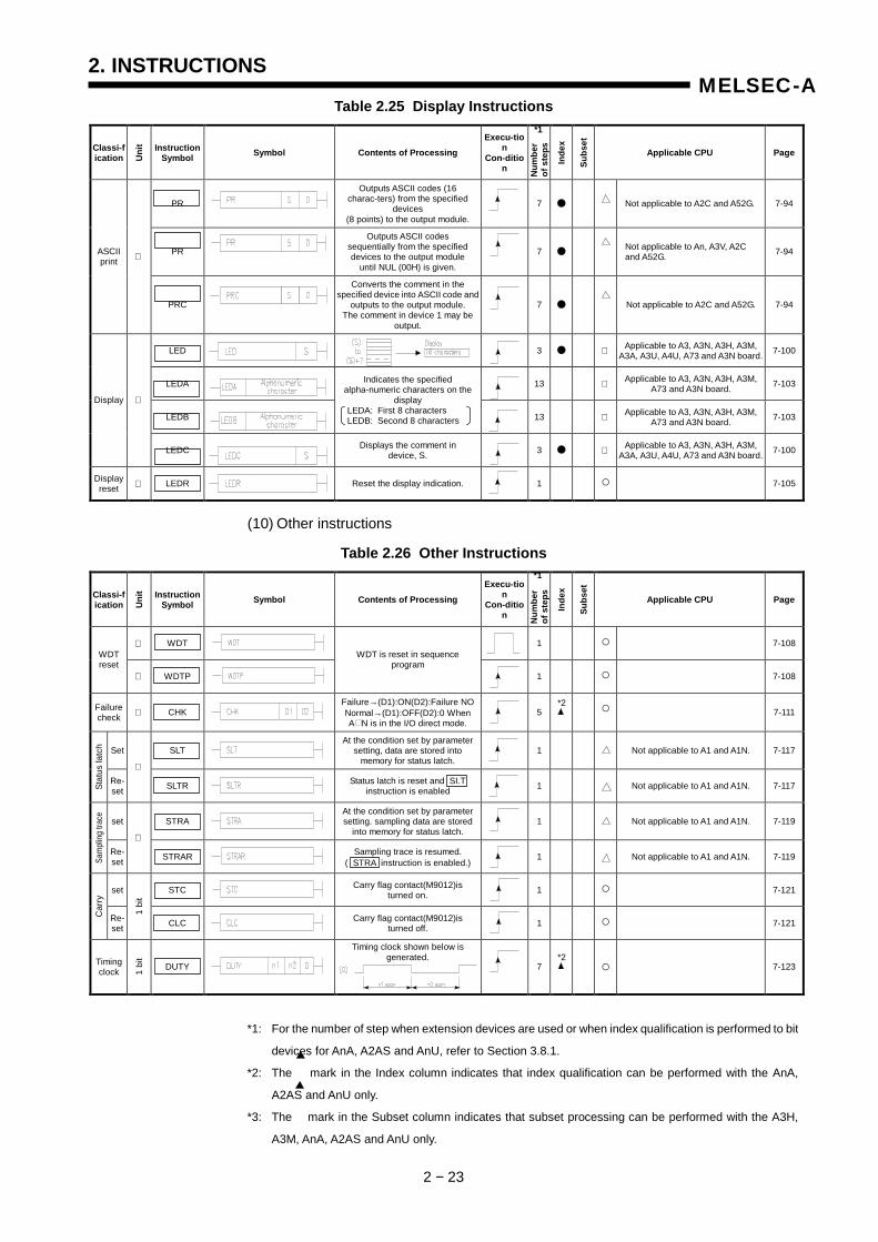
2. INSTRUCTIONS
2 − 23
MELSEC-ATable 2.25 Display Instructions
Classi-fication U
nit Instruction
Symbol Symbol Contents of Processing Execu-tio
n Con-ditio
n Num
ber
of s
teps
Inde
x
Subs
et
Applicable CPU Page
PR
Outputs ASCII codes (16 charac-ters) from the specified
devices (8 points) to the output module.
7 ● Not applicable to A2C and A52G. 7-94
PR
Outputs ASCII codes sequentially from the specified devices to the output module
until NUL (00H) is given.
7 ● Not applicable to An, A3V, A2C
and A52G. 7-94 ASCII print
PRC
Converts the comment in the specified device into ASCII code and
outputs to the output module. The comment in device 1 may be
output.
7 ● Not applicable to A2C and A52G. 7-94
LED
3 ● Applicable to A3, A3N, A3H, A3M,
A3A, A3U, A4U, A73 and A3N board. 7-100
LEDA
13 Applicable to A3, A3N, A3H, A3M,
A73 and A3N board. 7-103
LEDB
Indicates the specified alpha-numeric characters on the
display LEDA: First 8 characters LEDB: Second 8 characters
13 Applicable to A3, A3N, A3H, A3M,
A73 and A3N board. 7-103
Display
LEDC
Displays the comment in
device, S.
3 ● Applicable to A3, A3N, A3H, A3M,
A3A, A3U, A4U, A73 and A3N board. 7-100
Display reset LEDR
Reset the display indication.
1 ○ 7-105
(10) Other instructions
Table 2.26 Other Instructions
Classi-fication U
nit Instruction
Symbol Symbol Contents of Processing Execu-tio
n Con-ditio
n Num
ber
of s
teps
Inde
x
Subs
et
Applicable CPU Page
WDT
1 ○ 7-108
WDT reset
WDTP
WDT is reset in sequence program
1 ○ 7-108
Failure check CHK
Failure→(D1):ON(D2):Failure NO Normal→(D1):OFF(D2):0 When A N is in the I/O direct mode.
5 ○ 7-111
Set SLT
At the condition set by parameter setting, data are stored into
memory for status latch.
1 Not applicable to A1 and A1N. 7-117
Stat
us la
tch
Re-set
SLTR
Status latch is reset and SI.T
instruction is enabled
1 Not applicable to A1 and A1N. 7-117
set STRA
At the condition set by parameter setting. sampling data are stored
into memory for status latch.
1 Not applicable to A1 and A1N. 7-119
Sam
pling
trac
e
Re-set
STRAR
Sampling trace is resumed.
( STRA instruction is enabled.)
1 Not applicable to A1 and A1N. 7-119
set STC
Carry flag contact(M9012)is
turned on.
1 ○ 7-121
Car
ry
Re-set
1 bi
t
CLC
Carry flag contact(M9012)is
turned off.
1 ○ 7-121
Timing clock 1
bit
DUTY
Timing clock shown below is generated.
7 ○ 7-123
*1
*2
*2
*1
*1: For the number of step when extension devices are used or when index qualification is performed to bit
devices for AnA, A2AS and AnU, refer to Section 3.8.1.
*2: The mark in the Index column indicates that index qualification can be performed with the AnA,
A2AS and AnU only.
*3: The mark in the Subset column indicates that subset processing can be performed with the A3H,
A3M, AnA, A2AS and AnU only.
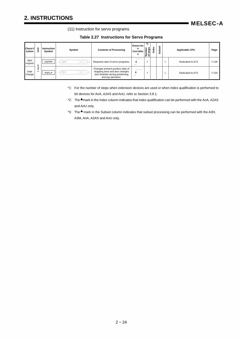
2. INSTRUCTIONS
2 − 24
MELSEC-A(11) Instruction for servo programs
Table 2.27 Instructions for Servo Programs
Classi-fication U
nit Instruction
Symbol Symbol Contents of Processing Execu-tio
n Con-ditio
n Num
ber
of s
teps
Inde
x
Subs
et
Applicable CPU Page
Start request DSFRP
Requests start of servo programs.
7 Dedicated to A73. 7-126
Date change
1 w
ord
PSFLP
Changes present position data of stopping axes and also changes axis feedrate during positioning
and jog operation.
7 Dedicated to A73. 7-130
*1: For the number of steps when extension devices are used or when index qualification is performed to
bit devices for AnA, A2AS and AnU, refer to Section 3.8.1.
*2: The mark in the Index column indicates that index qualification can be performed with the AnA, A2AS
and AnU only.
*3: The mark in the Subset column indicates that subset processing can be performed with the A3H,
A3M, AnA, A2AS and AnU only.
*1
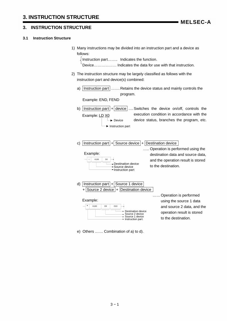
3. INSTRUCTION STRUCTURE
3 − 1
MELSEC-A3. INSTRUCTION STRUCTURE
3.1 Instruction Structure
1) Many instructions may be divided into an instruction part and a device as
follows:
Instruction part…….. Indicates the function.
Device……………… Indicates the data for use with that instruction.
2) The instruction structure may be largely classified as follows with the
instruction part and device(s) combined:
a) Instruction part ……. Retains the device status and mainly controls the
program.
Example: END, FEND
b) Instruction part + device …. Switches the device on/off, controls the
execution condition in accordance with the
device status, branches the program, etc.
c) Instruction part + Source device + Destination device
….. Operation is performed using the
destination data and source data,
and the operation result is stored
to the destination.
d) Instruction part + Source 1 device
+ Source 2 device + Destination device
…… Operation is performed
using the source 1 data
and source 2 data, and the
operation result is stored
to the destination.
e) Others ..….. Combination of a) to d).
Example: LD X0Device
Instruction part
Example:
Destination deviceSource deviceInstruction part
K100 D0
K100 D0 D10*
Destination deviceSource 2 deviceSource 1 deviceInstruction part.
Example:
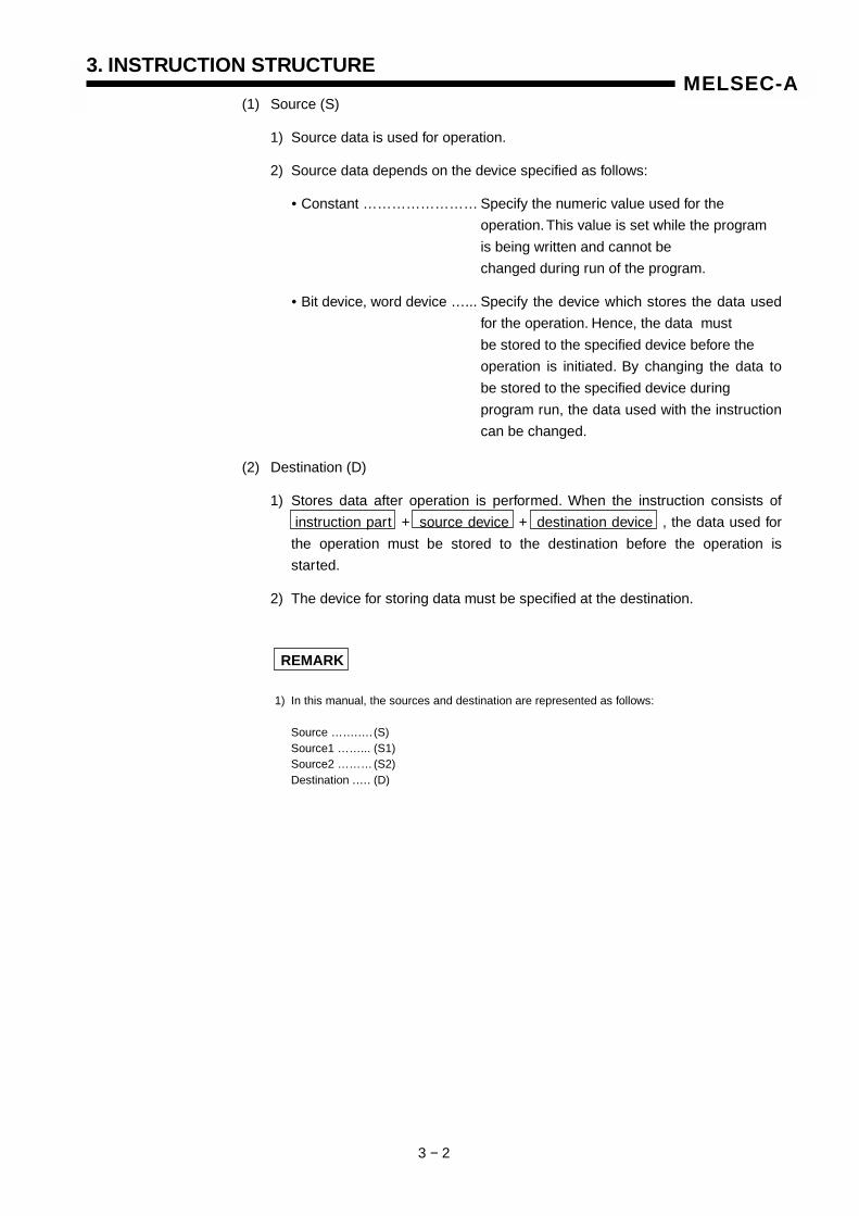
3. INSTRUCTION STRUCTURE
3 − 2
MELSEC-A(1) Source (S)
1) Source data is used for operation.
2) Source data depends on the device specified as follows:
• Constant …………………… Specify the numeric value used for the
operation. This value is set while the program
is being written and cannot be
changed during run of the program.
• Bit device, word device …... Specify the device which stores the data used
for the operation. Hence, the data must
be stored to the specified device before the
operation is initiated. By changing the data to
be stored to the specified device during
program run, the data used with the instruction
can be changed.
(2) Destination (D)
1) Stores data after operation is performed. When the instruction consists of
instruction part + source device + destination device , the data used for
the operation must be stored to the destination before the operation is
started.
2) The device for storing data must be specified at the destination.
REMARK
1) In this manual, the sources and destination are represented as follows:
Source …….….(S)Source1 ……... (S1)Source2 ………(S2)Destination .…. (D)
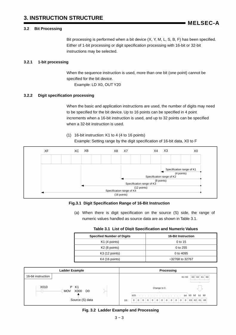
3. INSTRUCTION STRUCTURE
3 − 3
MELSEC-A3.2 Bit Processing
Bit processing is performed when a bit device (X, Y, M, L, S, B, F) has been specified.
Either of 1-bit processing or digit specification processing with 16-bit or 32-bit
instructions may be selected.
3.2.1 1-bit processing
When the sequence instruction is used, more than one bit (one point) cannot be
specified for the bit device.
Example: LD X0, OUT Y20
3.2.2 Digit specification processing
When the basic and application instructions are used, the number of digits may need
to be specified for the bit device. Up to 16 points can be specified in 4 point
increments when a 16-bit instruction is used, and up to 32 points can be specified
when a 32-bit instruction is used.
(1) 16-bit instruction: K1 to 4 (4 to 16 points)
Example: Setting range by the digit specification of 16-bit data, X0 to F
Fig.3.1 Digit Specification Range of 16-Bit Instruction
(a) When there is digit specification on the source (S) side, the range of
numeric values handled as source data are as shown in Table 3.1.
Specified Number of Digits 16-Bit Instruction
K1 (4 points) 0 to 15
K2 (8 points) 0 to 255
K3 (12 points) 0 to 4095
K4 (16 points) −32768 to 32767
Ladder Example Processing
16-bit instruction
XF XC XB X8 X7 X4 X3 X0
Specification range of K1(4 points)
Specification range of K2(8 points)
Specification range of K3(12 points)
Specification range of K4(16 points)
Table 3.1 List of Digit Specification and Numeric Values
D0
b3b4b15 b2 b1 b0
K1 X0
Change to 0.
0 0 0 0 0 0 0 0 0 0 0 0 X3 X2 X1 X0
X3 X2 X1 X0
Fig. 3.2 Ladder Example and Processing
Source (S) data
P K1MOV X000 D0
X010
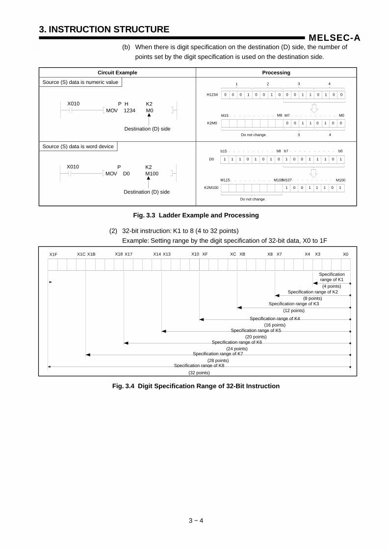
3. INSTRUCTION STRUCTURE
3 − 4
MELSEC-A(b) When there is digit specification on the destination (D) side, the number of
points set by the digit specification is used on the destination side.
Circuit Example Processing
Source (S) data is numeric value
Source (S) data is word device
Fig. 3.3 Ladder Example and Processing
(2) 32-bit instruction: K1 to 8 (4 to 32 points)
Example: Setting range by the digit specification of 32-bit data, X0 to 1F
Fig. 3.4 Digit Specification Range of 32-Bit Instruction
X1F X1C X1B X18 X17 X14 X13 X10 XC XBXF X8 X7 X4 X3 X0
Specificationrange of K1
(4 points)Specification range of K2
(8 points)Specification range of K3
(12 points)
Specification range of K4(16 points)
Specification range of K5(20 points)
Specification range of K6(24 points)
Specification range of K7
(28 points)Specification range of K8
(32 points)
K2M0
M15
Do not change .
1
H1234
M8 M7 M0
2 3 4
0 0 1 1
0 0 0 1 0 0 1 0 0 0 1 1
3 4
0 1 0 0
0 1 0 0
Destination (D) side
P HMOV 1234
X010 K2M0
K2M100
M115
Do not change .
D0
M108M107 M100
1 0 0 1
1 1 1 0 1 0 1 0 1 0 0 1 1 1 0 1
1 1 0 1
b15 b8 b7 b0
Destination (D) side
PMOV D0
X010 K2M100

3. INSTRUCTION STRUCTURE
3 − 5
MELSEC-A(3) When there is digit specification on the source (S) side, the range of numeric
values handled as source data are as shown in Table 3.2.
Table 3.2 List of Digit Specification and Handled Numeric Values
Specified Numberof Digits
32-Bit InstructionSpecified Number
of Digits32-Bit Instruction
K1 (4 points) 0 to 15 K5 (20 points) 0 to 1048575
K2 (8 points) 0 to 255 K6 (24 points) 0 to 167772165
K3 (12 points) 0 to 4095 K7 (28 points) 0 to 268435455
K4 (16 points) 0 to 65535 K8 (32 points) −2147483648 to 2147483647
Ladder Example Processing
32-bit instruction
Fig. 3.5 Ladder Example and Processing
(4) When there is digit specification on the destination (D) side, the number of
points set by the digit specification is used on the destination side.
Circuit Example Processing
Source (S) data is numeric value
Source (S) data is word device
Fig. 3.6 Ladder Example and Processing
POINT
For digit specification processing, any desired value can be used for the head
device number of bit devices.
D0
b3b4b15 b2 b1 b0
K1 X0
Change to 0.
0 0 0 0 0 0 0 0 0 0 0 0 X3 X2 X1 X0
X3 X2 X1 X0
D1 0 0 0 0 0 0 0 0 0 0 0 0 0 0 0 0
b31 b16
Change to 0.
Source (S) data
P K1DMOV X000 D0
X010
0 0 0 1
0 0 1 1 0 1 0 0 0 1 0 1 0 1 1 0
0 0 1 0
Do not change .
0 0 1 1 0 1 0 0 0 1 0 1 0 1 1 0
0 0 1 0
M15 M8 M7 M0
M31 M20 M19 M16
3 4 5 6
7 8 1 2
H78123456
0 1 1 1 1 0 0 0
K5M0
Destination (D) side
X010 P H K5DMOV 78123456 M0
Do not change .
1 1 1 0 0 1 0 0 0 1 0 1 1 1 0 1
0 1 1 1
M25 M18 M17 M10
M41 M30M29 M26
1 1 1 0 0 1 0 0 0 1 0 1 1 1 0 1
0 1 1 1
b15 b8 b7 b0
0 0 1 1 0 1 0 0 1 0 0 1
b15 b8 b7 b0
D1
D0
Destination (D) side
X010 P K5DMOV D0 M10
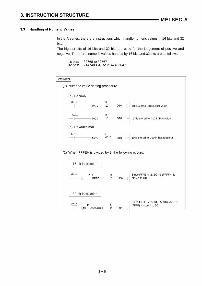
3. INSTRUCTION STRUCTURE
3 − 6
MELSEC-A
3.3 Handling of Numeric Values
In the A series, there are instructions which handle numeric values in 16 bits and 32 bits. The highest bits of 16 bits and 32 bits are used for the judgement of positive and negative. Therefore, numeric values handed by 16 bits and 32 bits are as follows:
POINTS
(1) Numeric value setting procedure
(a) Decimal
(b) Hexadecimal
(2) When FFFEH is divided by 2, the following occurs.
16 bits: -32768 to 32767 32 bits: -2147483648 to 2147483647
10 is stored D10 in BIN value.
-10 is stored to D10 in BIN value.
10 is stored to D10 in hexadecimal.
32-bit instruction
Since FFFE is 65534, 65534/2=32767 (7FFF) is stored to D0.
X010
X010
X010
MOV K 10 D10
MOV K- 10 D10
MOV H 0010 D10
16-bit instruction
Since FFFE is -2,-2/2=-1 (FFFFH) is stored to D0.
X010 D/
P H 0000FFFE D0
K 2
X010 P H K / FFFE 2 D0
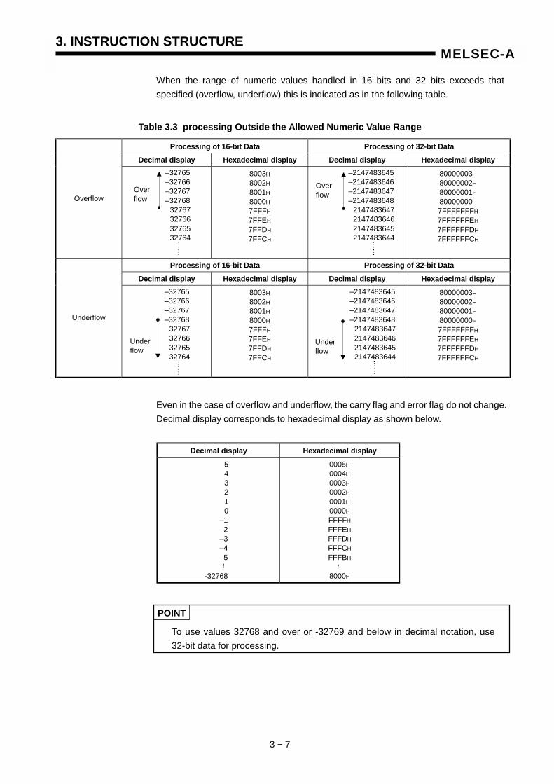
3. INSTRUCTION STRUCTURE
3 − 7
MELSEC-A
When the range of numeric values handled in 16 bits and 32 bits exceeds that specified (overflow, underflow) this is indicated as in the following table.
Table 3.3 processing Outside the Allowed Numeric Value Range
Processing of 16-bit Data Processing of 32-bit Data
Decimal display Hexadecimal display Decimal display Hexadecimal display
Overflow
8003H 8002H 8001H 8000H 7FFFH 7FFEH 7FFDH 7FFCH
80000003H 80000002H 80000001H 80000000H 7FFFFFFFH 7FFFFFFEH 7FFFFFFDH 7FFFFFFCH
Processing of 16-bit Data Processing of 32-bit Data
Decimal display Hexadecimal display Decimal display Hexadecimal display
Underflow
8003H 8002H 8001H 8000H 7FFFH 7FFEH 7FFDH 7FFCH
80000003H 80000002H 80000001H 80000000H 7FFFFFFFH 7FFFFFFEH 7FFFFFFDH 7FFFFFFCH
Even in the case of overflow and underflow, the carry flag and error flag do not change. Decimal display corresponds to hexadecimal display as shown below.
Decimal display Hexadecimal display
5 4 3 2 1 0 –1 –2 –3 –4 –5 -32768
0005H 0004H 0003H 0002H 0001H 0000H FFFFH FFFEH FFFDH FFFCH FFFBH
8000H
POINT
To use values 32768 and over or -32769 and below in decimal notation, use 32-bit data for processing.
Over flow
–32765 –32766 –32767 –32768 32767 32766 32765 32764
……
Over flow
–2147483645 –2147483646 –2147483647 –2147483648 2147483647 2147483646 2147483645 2147483644
Under flow
–32765 –32766 –32767 –32768 32767 32766 32765 32764
Under flow
–2147483645 –2147483646 –2147483647 –2147483648 2147483647 2147483646 2147483645 2147483644
……
……
……
~ ~
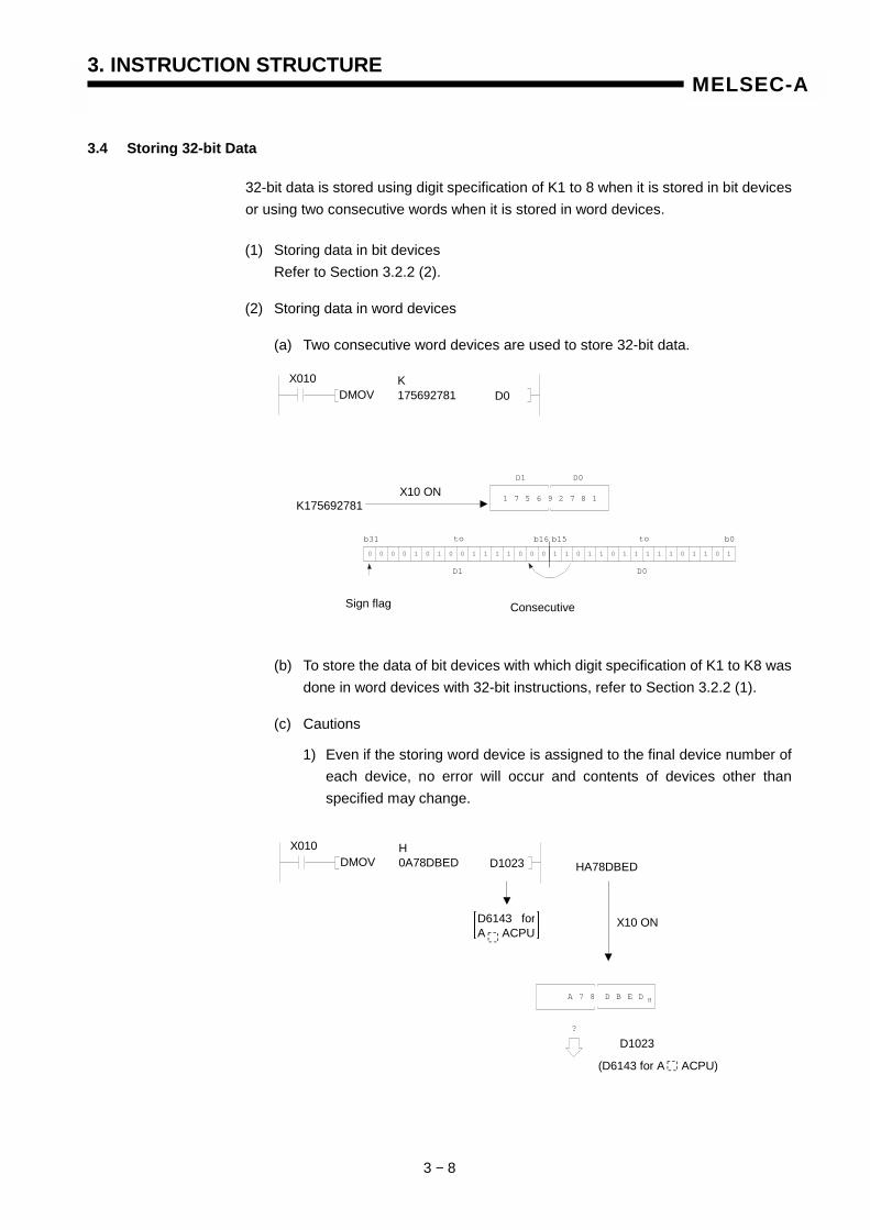
3. INSTRUCTION STRUCTURE
3 − 8
MELSEC-A
3.4 Storing 32-bit Data
32-bit data is stored using digit specification of K1 to 8 when it is stored in bit devices or using two consecutive words when it is stored in word devices.
(1) Storing data in bit devices Refer to Section 3.2.2 (2).
(2) Storing data in word devices
(a) Two consecutive word devices are used to store 32-bit data.
(b) To store the data of bit devices with which digit specification of K1 to K8 was done in word devices with 32-bit instructions, refer to Section 3.2.2 (1).
(c) Cautions
1) Even if the storing word device is assigned to the final device number of each device, no error will occur and contents of devices other than specified may change.
X010 DMOV
K 175692781 D0
K175692781 X10 ON
X010 DMOV
H 0A78DBED D1023 HA78DBED
D6143 for A ACPU
A 7 8 D B E D H
?
X10 ON
D1023
(D6143 for A ACPU)
b31 b16 b15 b0
D1 D0
0 0 0 0 1 0 1 0 0 1 1 1 1 0 0 0 1 1 0 1 1 0 1 1 1 1 1 0 1 1 0 1
to to
1 7 5 6 9 2 7 8 1
D1 D0
Sign flag Consecutive

3. INSTRUCTION STRUCTURE
3 − 9
MELSEC-A
2) Index registers can process 32-bit instructions when Z and V are used in pairs. In this case, Z is regarded as the lower 16-bit device, and therefore, V cannot be used in a 32-bit instruction. (Programs cannot be entered.)
If either of Z or V is specified for index qualification in the instruction, index qualification is performed regarding data in Z and V as 16-bit data even when 32-bit data is stored in Z and V.
REMARK
To handle 32-bit data with extension index registers Z1 to Z6 and V1 to V6 of AnA, A2AS and AnU, refer to Section 3.8.5.
3) If one of two consecutive word devices used to store 32-bit data is used in a 16-bit instruction, processing goes as follows.
X010 DMOV
H 0A78D8ED Z
V Z
A 7 8 D 8 E D H
HA78D8ED
X10 ON
X010 DMOV
H 12345678 Z
DMOV D2 D0 Z
⋅⋅⋅⋅⋅⋅ Data 12345678H is stored in Z and V.
⋅⋅⋅⋅⋅⋅ Data in D0 and D1 become equal to D(2+5678H) and D(3+5678H), respectively.
X010 DMOV
H 0A78D8ED D0
MOV
MOV
D0
D1
D10
D11
⋅⋅⋅⋅⋅⋅• When D0 is specified: Data b0 to b15 of D0 and D1 are handled as D0 data.
⋅⋅⋅⋅⋅⋅• When D1 is specified: Data b16 to b31 of D0 and D1 are handled as D1 data.
b31 b16 b15 b0
D1 D0
0 0 0 0 1 0 1 0 0 1 1 1 1 0 0 0 1 1 0 1 1 0 1 1 1 1 1 0 1 1 0 1
to to
b31 b16
D11
0 0 0 0 1 0 1 0 0 1 1 1 1 0 0 0
to b15 b0
D10
1 1 0 1 1 0 1 1 1 1 1 0 1 1 0 1
to
D 8 E D HH
A 7 8 D 8 E D H
A 7 8
HA78D8ED X10 ON
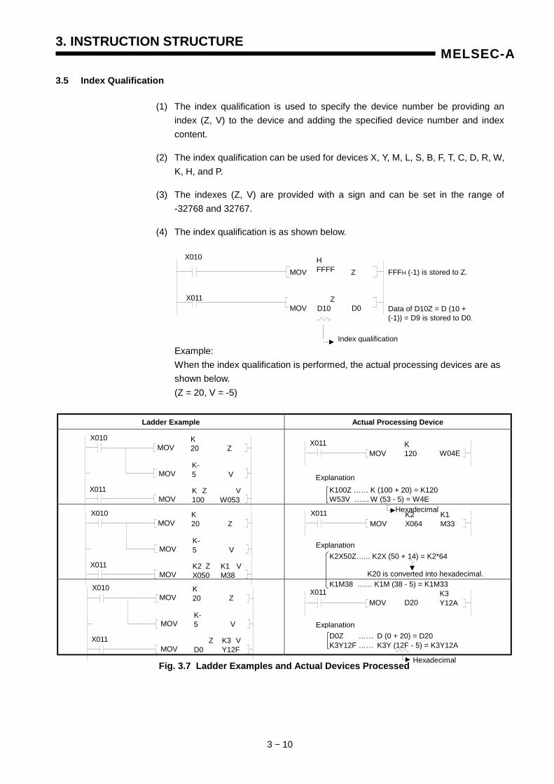
3. INSTRUCTION STRUCTURE
3 − 10
MELSEC-A
3.5 Index Qualification
(1) The index qualification is used to specify the device number be providing an index (Z, V) to the device and adding the specified device number and index content.
(2) The index qualification can be used for devices X, Y, M, L, S, B, F, T, C, D, R, W, K, H, and P.
(3) The indexes (Z, V) are provided with a sign and can be set in the range of -32768 and 32767.
(4) The index qualification is as shown below.
Example: When the index qualification is performed, the actual processing devices are as shown below. (Z = 20, V = -5)
Ladder Example Actual Processing Device
X010
MOV H FFFF Z
X011 MOV
Z D10 D0
FFFH (-1) is stored to Z.
Data of D10Z = D (10 + (-1)) = D9 is stored to D0.
Index qualification
X010
X011
MOV K 20 Z
MOV K- 5 V
MOV K Z 100
V W053
X010
X011
MOV K 20 Z
MOV K- 5 V
MOV K2 Z X050
K1 V M38
X010
X011
MOV K 20 Z
MOV K- 5 V
MOV Z D0
K3 V Y12F
X011 MOV
K 120 W04E
Explanation K100Z …… K (100 + 20) = K120 W53V …… W (53 - 5) = W4E
Hexadecimal X011 MOV
K2 X064
K1 M33
Explanation K2X50Z…... K2X (50 + 14) = K2*64 K1M38 …… K1M (38 - 5) = K1M33
K20 is converted into hexadecimal.
X011 MOV D20
K3 Y12A
Explanation D0Z …… D (0 + 20) = D20 K3Y12F …… K3Y (12F - 5) = K3Y12A
Hexadecimal Fig. 3.7 Ladder Examples and Actual Devices Processed
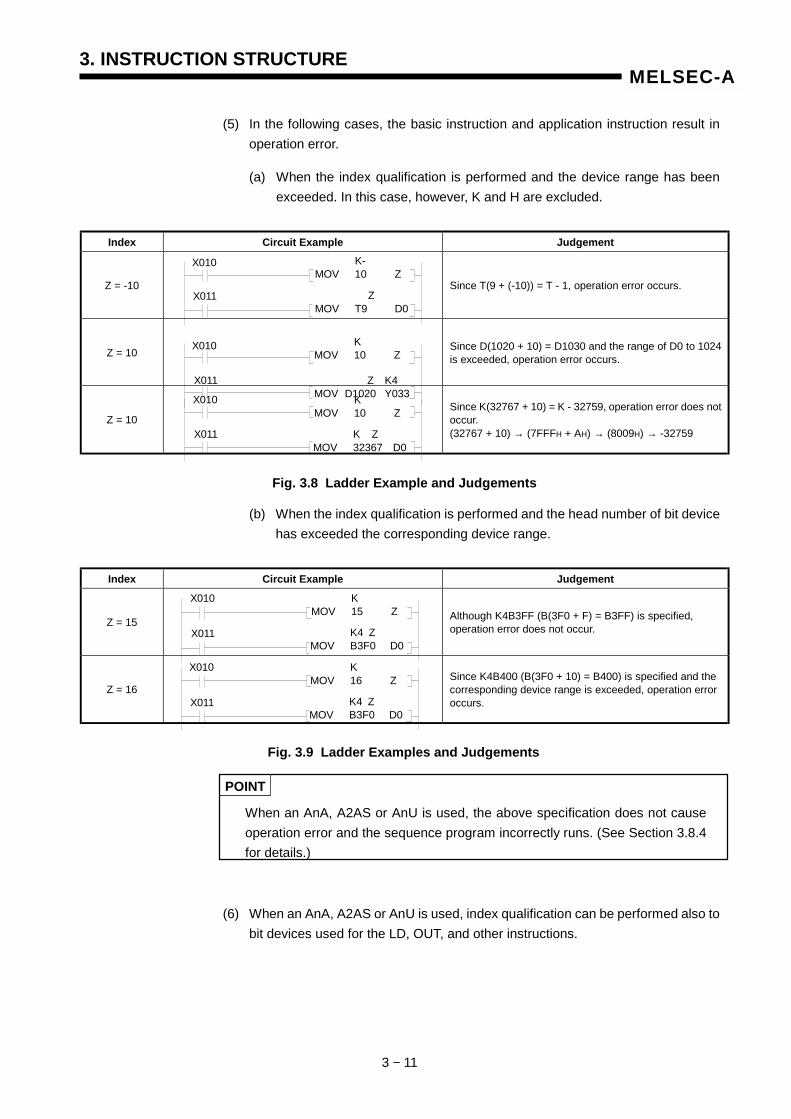
3. INSTRUCTION STRUCTURE
3 − 11
MELSEC-A
(5) In the following cases, the basic instruction and application instruction result in operation error.
(a) When the index qualification is performed and the device range has been exceeded. In this case, however, K and H are excluded.
Index Circuit Example Judgement
Z = -10
Since T(9 + (-10)) = T - 1, operation error occurs.
Z = 10
Since D(1020 + 10) = D1030 and the range of D0 to 1024 is exceeded, operation error occurs.
Z = 10
Since K(32767 + 10) = K - 32759, operation error does not occur. (32767 + 10) → (7FFFH + AH) → (8009H) → -32759
(b) When the index qualification is performed and the head number of bit device has exceeded the corresponding device range.
Index Circuit Example Judgement
Z = 15
Although K4B3FF (B(3F0 + F) = B3FF) is specified, operation error does not occur.
Z = 16
Since K4B400 (B(3F0 + 10) = B400) is specified and the corresponding device range is exceeded, operation error occurs.
POINT
When an AnA, A2AS or AnU is used, the above specification does not cause operation error and the sequence program incorrectly runs. (See Section 3.8.4 for details.)
(6) When an AnA, A2AS or AnU is used, index qualification can be performed also to bit devices used for the LD, OUT, and other instructions.
X010 K- MOV 10 Z
X011 Z MOV T9 D0
X010 K MOV 10 Z
X011 Z K4 MOV D1020 Y033 X010 K MOV 10 Z
X011 K Z MOV 32367 D0
X010 K MOV 15 Z
X011 K4 Z MOV B3F0 D0
X010 K MOV 16 Z
X011 K4 Z MOV B3F0 D0
Fig. 3.8 Ladder Example and Judgements
Fig. 3.9 Ladder Examples and Judgements
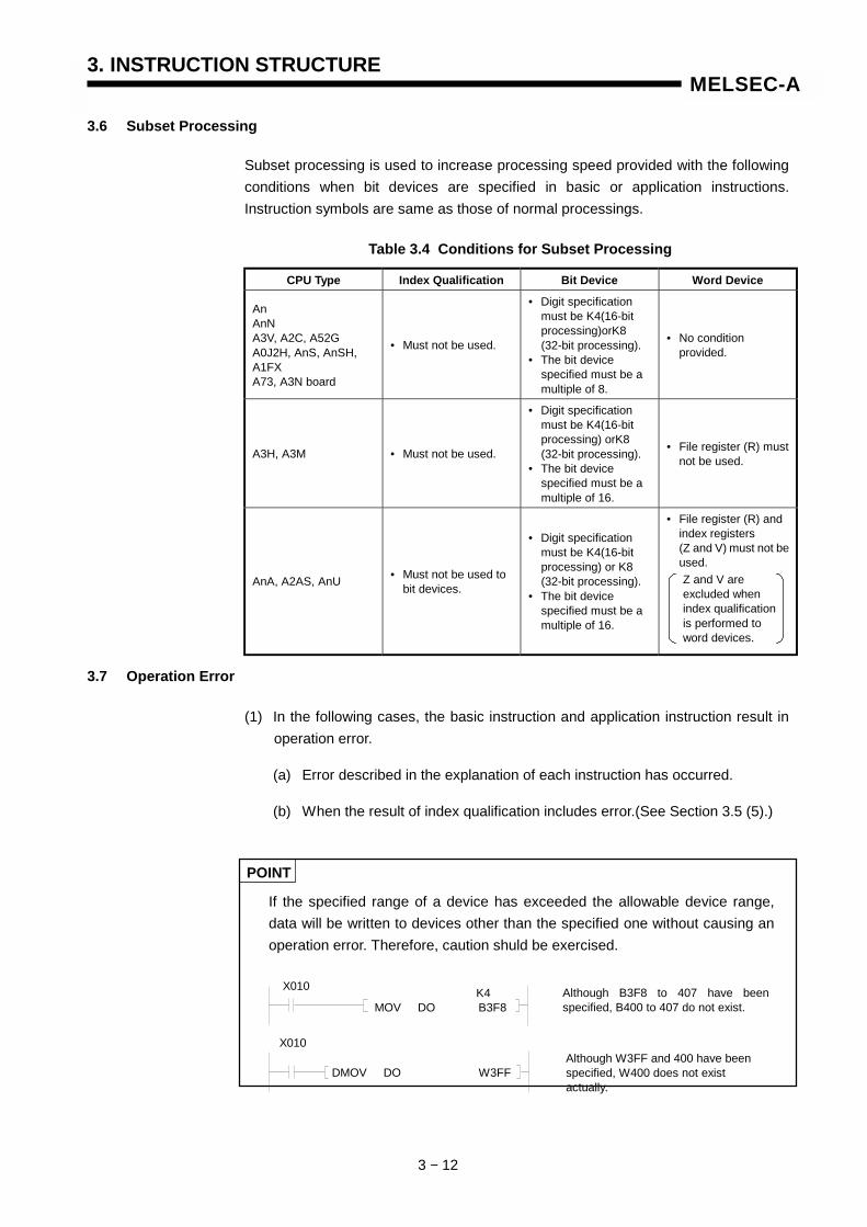
3. INSTRUCTION STRUCTURE
3 − 12
MELSEC-A
3.6 Subset Processing
Subset processing is used to increase processing speed provided with the following conditions when bit devices are specified in basic or application instructions. Instruction symbols are same as those of normal processings.
CPU Type Index Qualification Bit Device Word Device
An AnN A3V, A2C, A52G A0J2H, AnS, AnSH, A1FX A73, A3N board
• Must not be used.
• Digit specification must be K4(16-bit processing)orK8 (32-bit processing).
• The bit device specified must be a multiple of 8.
• No condition provided.
A3H, A3M • Must not be used.
• Digit specification must be K4(16-bit processing) orK8 (32-bit processing).
• The bit device specified must be a multiple of 16.
• File register (R) must not be used.
AnA, A2AS, AnU • Must not be used to bit devices.
• Digit specification must be K4(16-bit processing) or K8 (32-bit processing).
• The bit device specified must be a multiple of 16.
• File register (R) and index registers (Z and V) must not be used.
3.7 Operation Error
(1) In the following cases, the basic instruction and application instruction result in operation error.
(a) Error described in the explanation of each instruction has occurred.
(b) When the result of index qualification includes error.(See Section 3.5 (5).)
POINT
If the specified range of a device has exceeded the allowable device range, data will be written to devices other than the specified one without causing an operation error. Therefore, caution shuld be exercised.
Z and V are excluded when index qualification is performed to word devices.
Table 3.4 Conditions for Subset Processing
Although B3F8 to 407 have been specified, B400 to 407 do not exist.
Although W3FF and 400 have been specified, W400 does not exist actually.
X010
MOV DO B3F8 K4
X010
DMOV DO W3FF
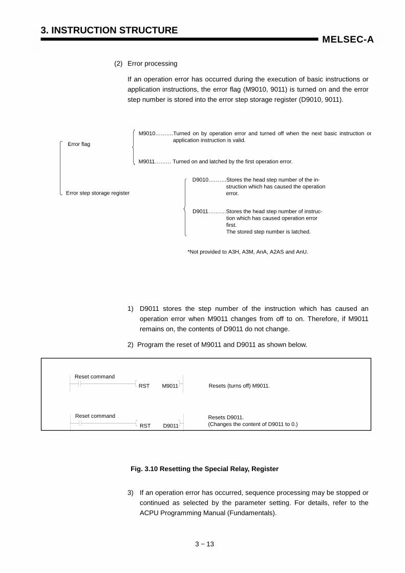
3. INSTRUCTION STRUCTURE
3 − 13
MELSEC-A
(2) Error processing
If an operation error has occurred during the execution of basic instructions or application instructions, the error flag (M9010, 9011) is turned on and the error step number is stored into the error step storage register (D9010, 9011).
1) D9011 stores the step number of the instruction which has caused an operation error when M9011 changes from off to on. Therefore, if M9011 remains on, the contents of D9011 do not change.
2) Program the reset of M9011 and D9011 as shown below.
Fig. 3.10 Resetting the Special Relay, Register
3) If an operation error has occurred, sequence processing may be stopped or continued as selected by the parameter setting. For details, refer to the ACPU Programming Manual (Fundamentals).
Error flag
*Not provided to A3H, A3M, AnA, A2AS and AnU.
M9010……….Turned on by operation error and turned off when the next basic instruction or application instruction is valid.
M9011……… Turned on and latched by the first operation error.
D9010……….Stores the head step number of the in- struction which has caused the operation error.
D9011……….Stores the head step number of instruc- tion which has caused operation error first. The stored step number is latched.
Error step storage register
Resets (turns off) M9011.
Resets D9011. (Changes the content of D9011 to 0.)
Reset command
Reset command
RST M9011
RST D9011
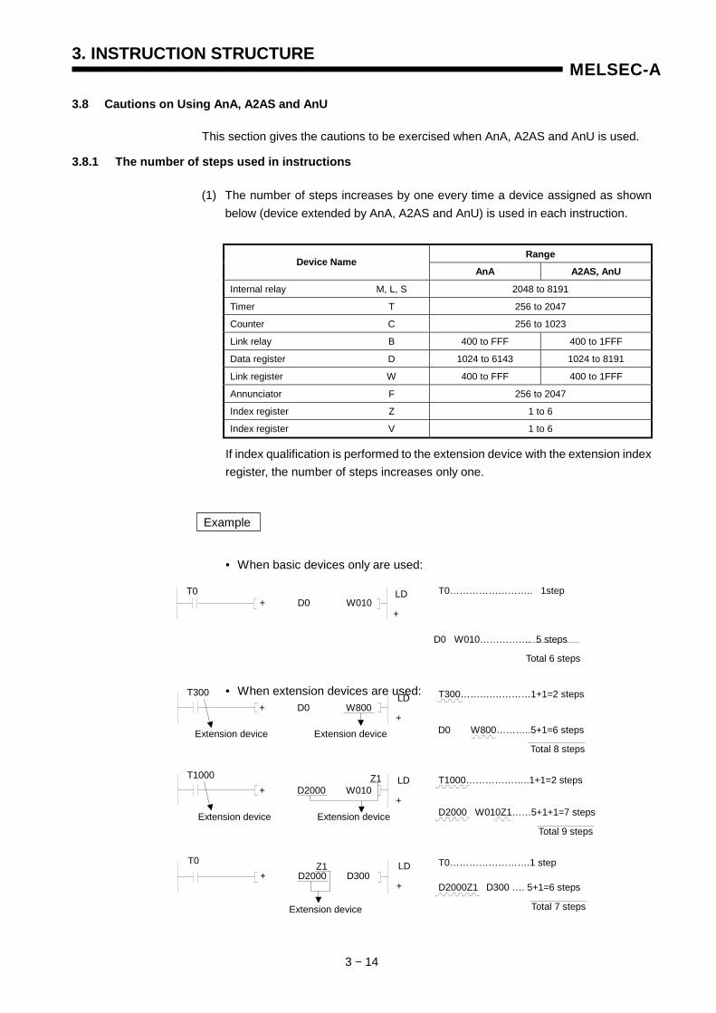
3. INSTRUCTION STRUCTURE
3 − 14
MELSEC-A
3.8 Cautions on Using AnA, A2AS and AnU
This section gives the cautions to be exercised when AnA, A2AS and AnU is used.
3.8.1 The number of steps used in instructions
(1) The number of steps increases by one every time a device assigned as shown below (device extended by AnA, A2AS and AnU) is used in each instruction.
Range Device Name
AnA A2AS, AnU
Internal relay M, L, S 2048 to 8191
Timer T 256 to 2047
Counter C 256 to 1023
Link relay B 400 to FFF 400 to 1FFF
Data register D 1024 to 6143 1024 to 8191
Link register W 400 to FFF 400 to 1FFF
Annunciator F 256 to 2047
Index register Z 1 to 6
Index register V 1 to 6
If index qualification is performed to the extension device with the extension index register, the number of steps increases only one.
Example
• When basic devices only are used:
• When extension devices are used:
D0 W010……………. 5 steps
Total 6 steps
T0…………………….. 1step T0 + D0 W010
LD
+
T300……….…………1+1=2 steps
D0 W800………..5+1=6 steps
Total 8 steps
D2000Z1 D300 …. 5+1=6 steps
Total 7 steps
Extension device Extension device
T300 + D0 W800
LD
+
T1000………………..1+1=2 steps
D2000 W010Z1……5+1+1=7 steps
Total 9 steps
Extension device
T0…………………….1 step
Extension device Extension device
T1000 + D2000 W010
LD
+
Z1
T0 + D2000 D300
LD
+
Z1

3. INSTRUCTION STRUCTURE
3 − 15
MELSEC-A
(2) If index qualification is used in a 1-step sequence instruction (such as LD, OUT), the number of steps increases one.
Example
• When index qualification is not used:
• When index qualification is used:
REMARK
Even when index qualification is used in a 1-step sequence instruction (such as LD, OUT) with index registers (Z1 to Z6, V1 to V6) extended by AnA, A2AS and AnU, the number of steps increases only one.
Example
LD X0 ……………....1 step
OUT Y40 ……….…..1 step
Total 2 steps
LD X0Z………………1+1=2 steps
OUT Y40…………….1 step
Total 3 steps Index qualification
( )X000
Y040
LD X0Z3……………..1+1=2 steps
OUT Y40V6…………1+1=2 steps
Total 4 steps
( )X000
Y040 V6
Z3
( )
X000 Y040 Z
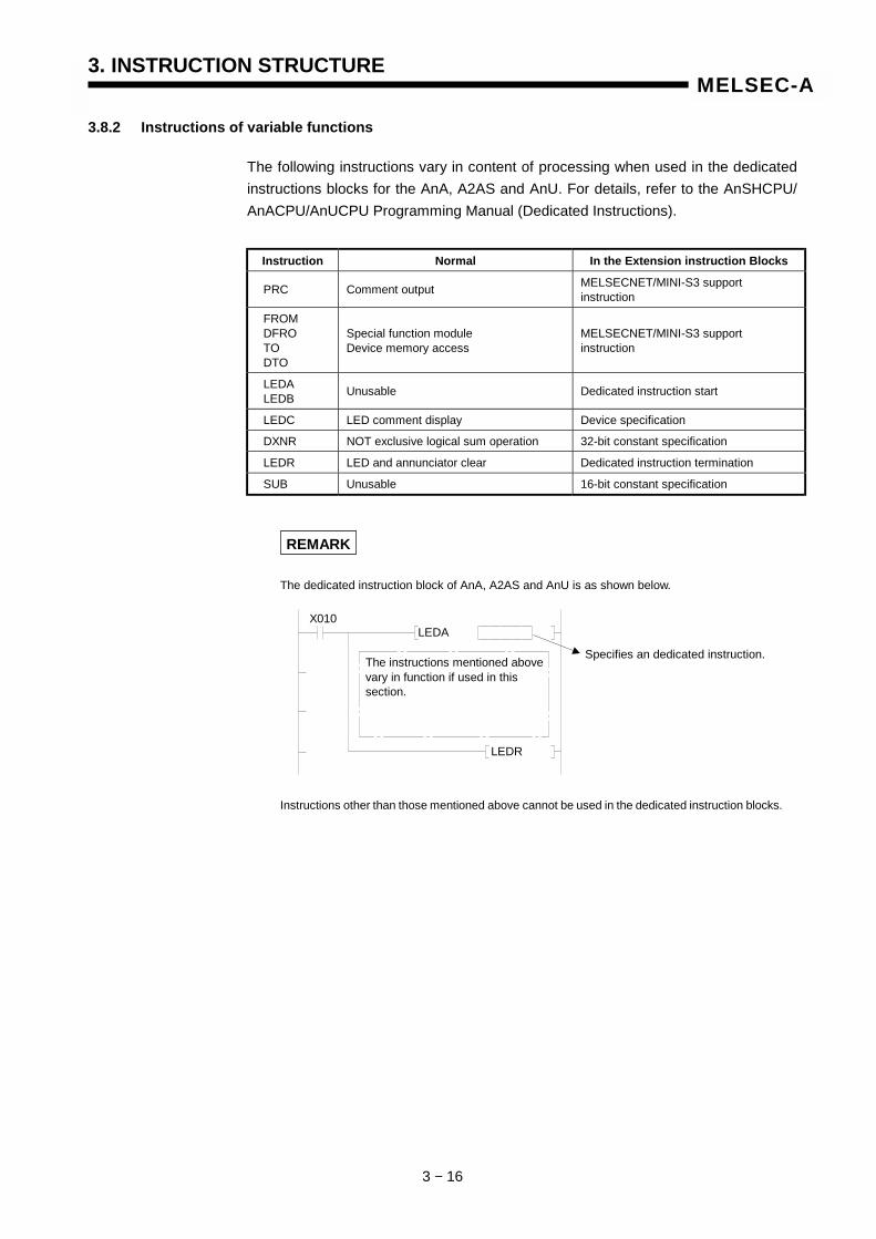
3. INSTRUCTION STRUCTURE
3 − 16
MELSEC-A
3.8.2 Instructions of variable functions
The following instructions vary in content of processing when used in the dedicated instructions blocks for the AnA, A2AS and AnU. For details, refer to the AnSHCPU/ AnACPU/AnUCPU Programming Manual (Dedicated Instructions).
Instruction Normal In the Extension instruction Blocks
PRC Comment output MELSECNET/MINI-S3 support instruction
FROM DFRO TO DTO
Special function module Device memory access
MELSECNET/MINI-S3 support instruction
LEDA LEDB Unusable Dedicated instruction start
LEDC LED comment display Device specification
DXNR NOT exclusive logical sum operation 32-bit constant specification
LEDR LED and annunciator clear Dedicated instruction termination
SUB Unusable 16-bit constant specification
REMARK
The dedicated instruction block of AnA, A2AS and AnU is as shown below.
Instructions other than those mentioned above cannot be used in the dedicated instruction blocks.
X010 LEDA
LEDR
The instructions mentioned above vary in function if used in this section.
Specifies an dedicated instruction.
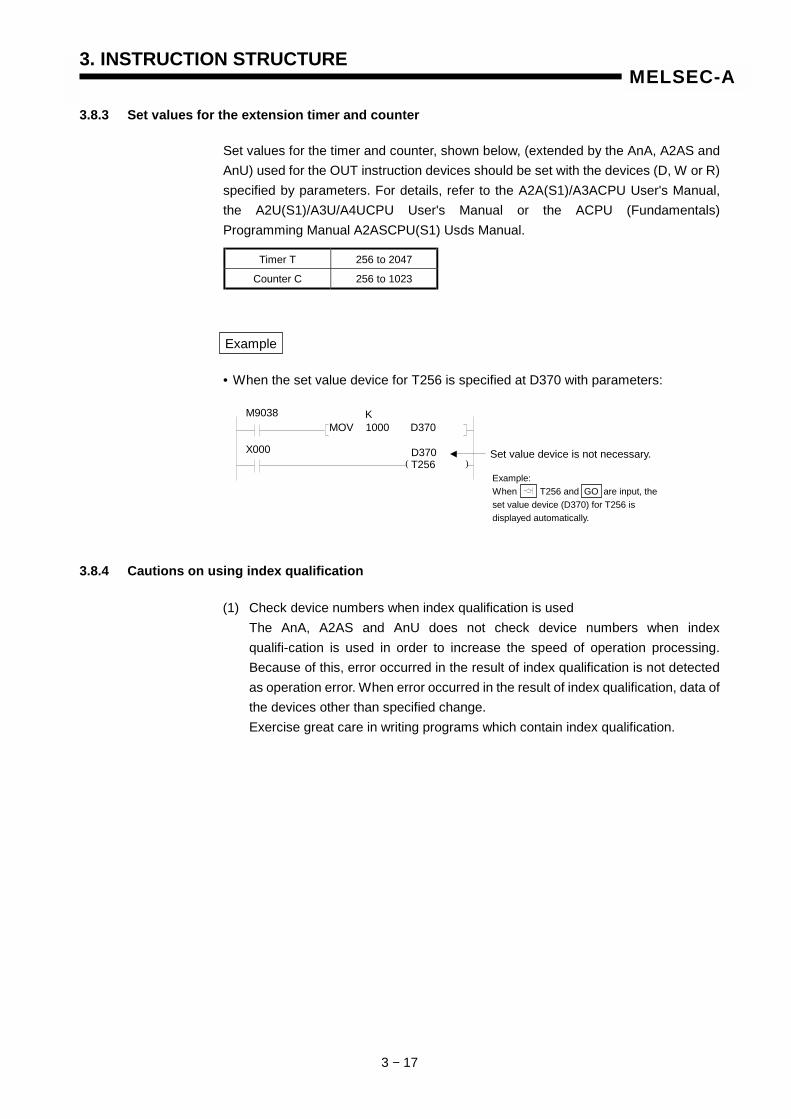
3. INSTRUCTION STRUCTURE
3 − 17
MELSEC-A
3.8.3 Set values for the extension timer and counter
Set values for the timer and counter, shown below, (extended by the AnA, A2AS and AnU) used for the OUT instruction devices should be set with the devices (D, W or R) specified by parameters. For details, refer to the A2A(S1)/A3ACPU User's Manual, the A2U(S1)/A3U/A4UCPU User's Manual or the ACPU (Fundamentals) Programming Manual A2ASCPU(S1) Usds Manual.
Timer T 256 to 2047
Counter C 256 to 1023
Example
• When the set value device for T256 is specified at D370 with parameters:
3.8.4 Cautions on using index qualification
(1) Check device numbers when index qualification is used The AnA, A2AS and AnU does not check device numbers when index qualifi-cation is used in order to increase the speed of operation processing. Because of this, error occurred in the result of index qualification is not detected as operation error. When error occurred in the result of index qualification, data of the devices other than specified change. Exercise great care in writing programs which contain index qualification.
( )
M9038 K MOV 1000 D370
D370 T256
Set value device is not necessary. X000
Example: When T256 and GO are input, the set value device (D370) for T256 is displayed automatically.
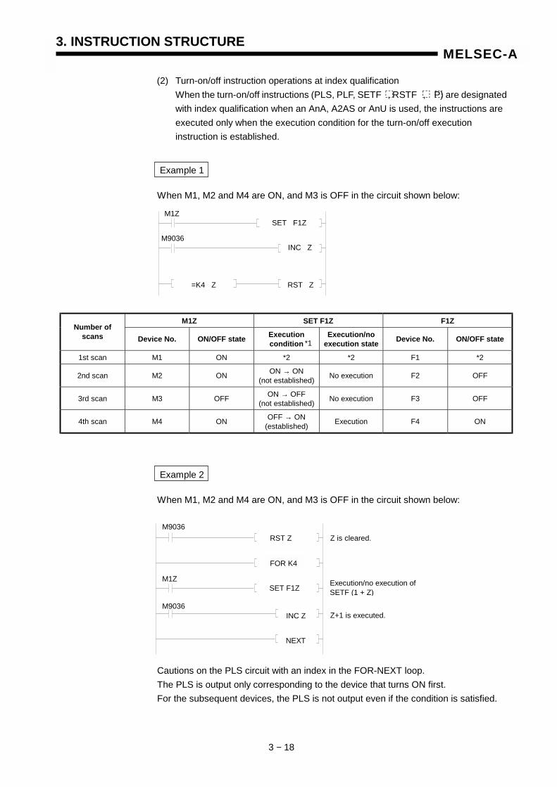
3. INSTRUCTION STRUCTURE
3 − 18
MELSEC-A
(2) Turn-on/off instruction operations at index qualification When the turn-on/off instructions (PLS, PLF, SETF , RSTF , P) are designated with index qualification when an AnA, A2AS or AnU is used, the instructions are executed only when the execution condition for the turn-on/off execution instruction is established.
Example 1
When M1, M2 and M4 are ON, and M3 is OFF in the circuit shown below:
M1Z SET F1Z F1Z Number of
scans Device No. ON/OFF state Execution condition
Execution/no execution state Device No. ON/OFF state
1st scan M1 ON *2 *2 F1 *2
2nd scan M2 ON ON → ON (not established) No execution F2 OFF
3rd scan M3 OFF ON → OFF (not established) No execution F3 OFF
4th scan M4 ON OFF → ON (established) Execution F4 ON
Example 2
When M1, M2 and M4 are ON, and M3 is OFF in the circuit shown below:
Cautions on the PLS circuit with an index in the FOR-NEXT loop. The PLS is output only corresponding to the device that turns ON first. For the subsequent devices, the PLS is not output even if the condition is satisfied.
M1Z SET F1Z
INC Z M9036
RST Z =K4 Z
M9036
M1Z
RST Z
FOR K4
Z is cleared.
SET F1Z Execution/no execution of SETF (1 + Z)
INC Z
NEXT
*1
M9036 Z+1 is executed.
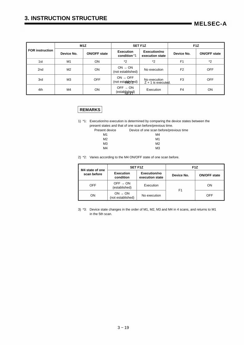
3. INSTRUCTION STRUCTURE
3 − 19
MELSEC-A
M1Z SET F1Z F1Z
FOR instruction Device No. ON/OFF state Execution
condition Execution/no
execution state Device No. ON/OFF state
1st M1 ON *2 *2 F1 *2
2nd M2 ON ON → ON (not established) No execution F2 OFF
3rd M3 OFF ON → OFF (not established) No execution F3 OFF
4th M4 ON OFF → ON (established) Execution F4 ON
REMARKS
1) *1: Execution/no execution is determined by comparing the device states between the present states and that of one scan before/previous time. Present device Device of one scan before/previous time M1 M4 M2 M1 M3 M2 M4 M3 2) *2: Varies according to the M4 ON/OFF state of one scan before.
SET F1Z F1Z M4 state of one
scan before Execution condition
Execution/no execution state Device No. ON/OFF state
OFF OFF → ON (established) Execution ON
ON ON → ON (not established) No execution
F1 OFF
3) *3: Device state changes in the order of M1, M2, M3 and M4 in 4 scans, and returns to M1 in the 5th scan.
INC Z Z + 1 is executed.
NEXT
*1
3. INSTRUCTION STRUCTURE
3 − 20
MELSEC-A
3.8.5 Storing 32-bit data in index registers
It is possible to store 32-bit data in the index registers (Z1 to Z6, V1 to V6) extended by the AnA, A2AS and AnU. The following index registers are used in pairs to store 32-bit data.
1) Z1 and V1 2) Z2 and V2 3) Z3 and V3 4) Z4 and V4 5) Z5 and V5 6) Z6 and V6
Any pairs other than those mentioned above cannot store 32-bit data. If one of paired devices is specified for index qualification in an instruction, data in such index register is regarded as 16-bit data for index qualification.
Since Zn is regarded as the device for lower 16 bits, Vn cannot be used in 32-bitinstructions.(Programs cannot be entered.)
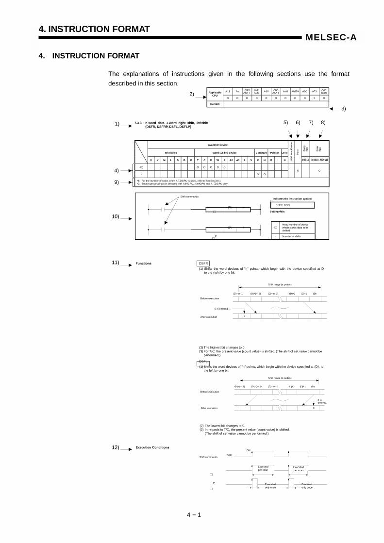
4. INSTRUCTION FORMAT
4 − 1
MELSEC-A
4. INSTRUCTION FORMAT
The explanations of instructions given in the following sections use the format
described in this section.
Available Device
Bit device Word (16-bit) device Constant Pointer Level
X Y M L S B F T C D W R A0 A1 Z V K H P I N M9012 (M9010, M9011)
(D) O O O O O
n O O
O O
*1: For the number of steps when A ACPU is used, refer to Section 3.8.1*2: Subset processing can be used with A3HCPU, A3MCPU and A ACPU only
A1S AnAnN
AnN-FA3HA3M A3V
AnAAnA-F AnU A0J2H A2C A73
A3NboardApplicable
CPUO O O O O O O O O X O
Remark
7.3.3 n-word data 1-word right shift, leftshift(DSFR, DSFRP, DSFL, DSFLP)
(D)Head number of devicewhich stores data to beshifted
n Number of shifts
Setting data
DSFR, DSFL
Indicates the instruction symbol.Shift commands
(D) n
(D) n
P
Dig
itsp
ecifi
catio
n
Functions DSFR
(1) Shifts the word devices of "n" points, which begin with the device specified at D,to the right by one bit.
(2) The highest bit changes to 0.(3) For T/C, the present value (count value) is shifted. (The shift of set value cannot be
performed.)
DSFL
(1) Shifts the word devices of "n" points, which begin with the device specified at (D), tothe left by one bit.
(2) The lowest bit changes to 0.(3) In regards to T/C, the present value (count value) is shifted.
(The shift of set value cannot be performed.)
Execution Conditions
OFF
ON
Executedper scan
Executedonly once
P
Shift commands
Executedper scan
Executedonly once
2)
3)
1)
4)
9)
10)
11)
12)
Car
ryfla
g
Err
orfla
g
8)7)6)5)
0
(D)+(n- 1) (D)+(n- 2) (D)+(n- 3) (D)+2 (D)+1 (D)
Shift range (n points)
0 is entered.
Before execution
After execution
Shift range (n points)
0 is entered.
(D)+(n- 1) (D)+(n- 2) (D)+(n- 3) (D)+2 (D)+1 (D)
Shift range (n points)
0
0 isentered.
Before execution
After execution
Shift range (n points)
0 isentered.
Inde
x

4. INSTRUCTION FORMAT
4 − 2
MELSEC-A
Operation Error In the following case, operation error occurs and the error flag turns on."n" is a negative value.
13)
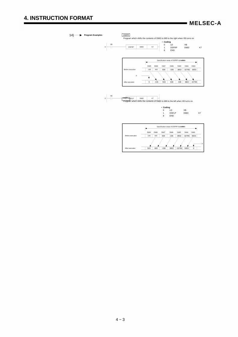
4. INSTRUCTION FORMAT
4 − 3
MELSEC-A
0
XB
DSFLP D683 K7
Program Examples DSFR
Program which shifts the contents of D683 to 689 to the right when XB turns on.
• Coding0 LD XB1 DSFRP D683 K78 END
Specification range of DSFRP instruction
0
D688D689 D687 D686 D685 D684 D683
-100 503 600 -336 3802 -32765 5003
0 -100 503 600 -336 3802 -32765
Before execution
After execution
Specification range of DSFRP instruction
DSFL
Program which shifts the contents of D683 to 689 to the left when XB turns on.
• Coding0 LD XB1 DSFLP D683 K78 END
Specification range of DSFRP instruction
0
D688D689 D687 D686 D685 D684 D683
-100 503 600 -336 3802 -32765 5003
503 600 -336 3802 -32765 5003 0
Before execution
After execution
Specification range of DSFRP instruction
14)
0
XB
DSFRP D683 K7
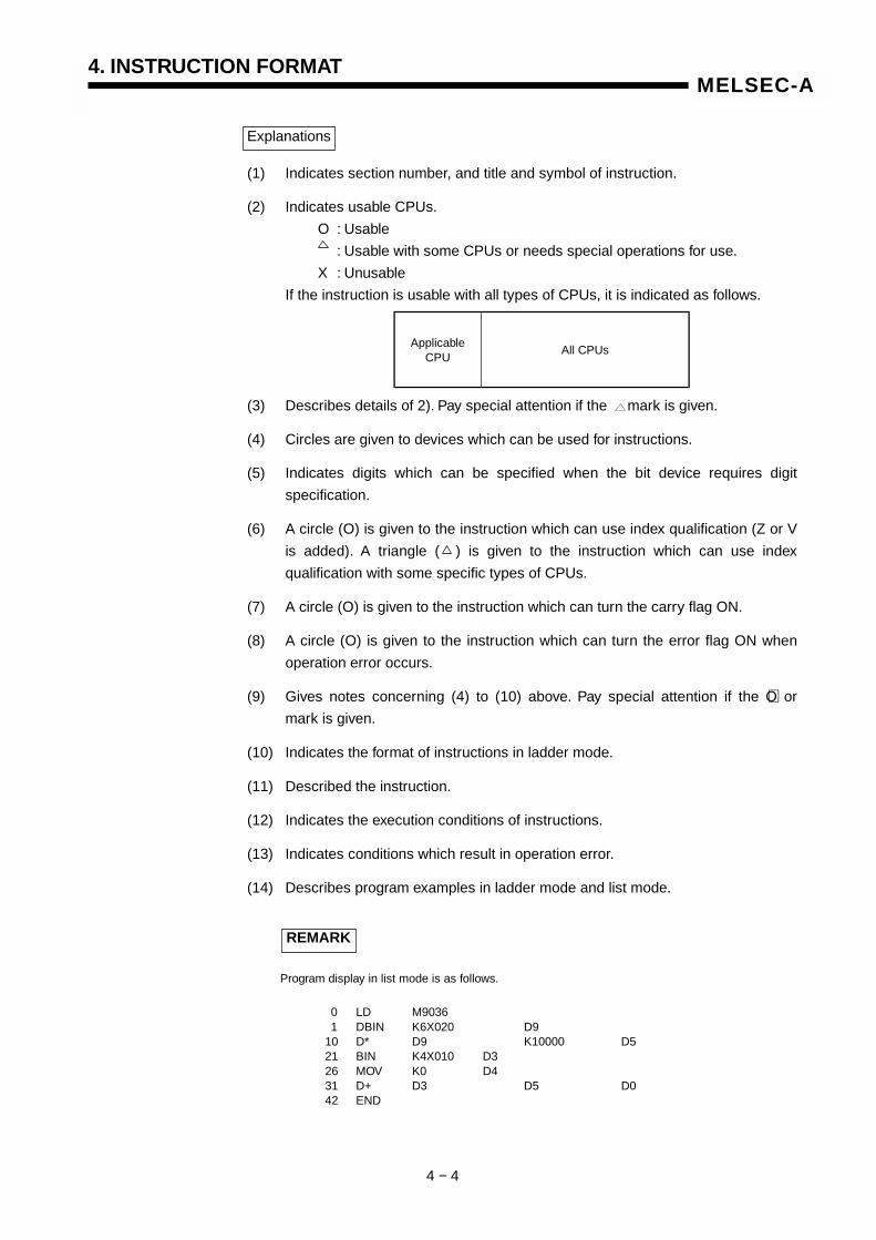
4. INSTRUCTION FORMAT
4 − 4
MELSEC-A
Explanations
(1) Indicates section number, and title and symbol of instruction.
(2) Indicates usable CPUs.
O : Usable
: Usable with some CPUs or needs special operations for use.
X : Unusable
If the instruction is usable with all types of CPUs, it is indicated as follows.
ApplicableCPU
All CPUs
(3) Describes details of 2). Pay special attention if the mark is given.
(4) Circles are given to devices which can be used for instructions.
(5) Indicates digits which can be specified when the bit device requires digit
specification.
(6) A circle (O) is given to the instruction which can use index qualification (Z or V
is added). A triangle ( ) is given to the instruction which can use index
qualification with some specific types of CPUs.
(7) A circle (O) is given to the instruction which can turn the carry flag ON.
(8) A circle (O) is given to the instruction which can turn the error flag ON when
operation error occurs.
(9) Gives notes concerning (4) to (10) above. Pay special attention if the O or
mark is given.
(10) Indicates the format of instructions in ladder mode.
(11) Described the instruction.
(12) Indicates the execution conditions of instructions.
(13) Indicates conditions which result in operation error.
(14) Describes program examples in ladder mode and list mode.
REMARK
Program display in list mode is as follows.
0 LD M90361 DBIN K6X020 D9
10 D* D9 K10000 D521 BIN K4X010 D326 MOV K0 D431 D+ D3 D5 D042 END
∗
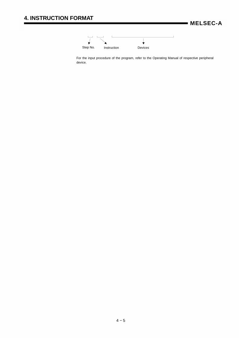
4. INSTRUCTION FORMAT
4 − 5
MELSEC-A
For the input procedure of the program, refer to the Operating Manual of respective peripheraldevice.
Step No. Instruction Devices
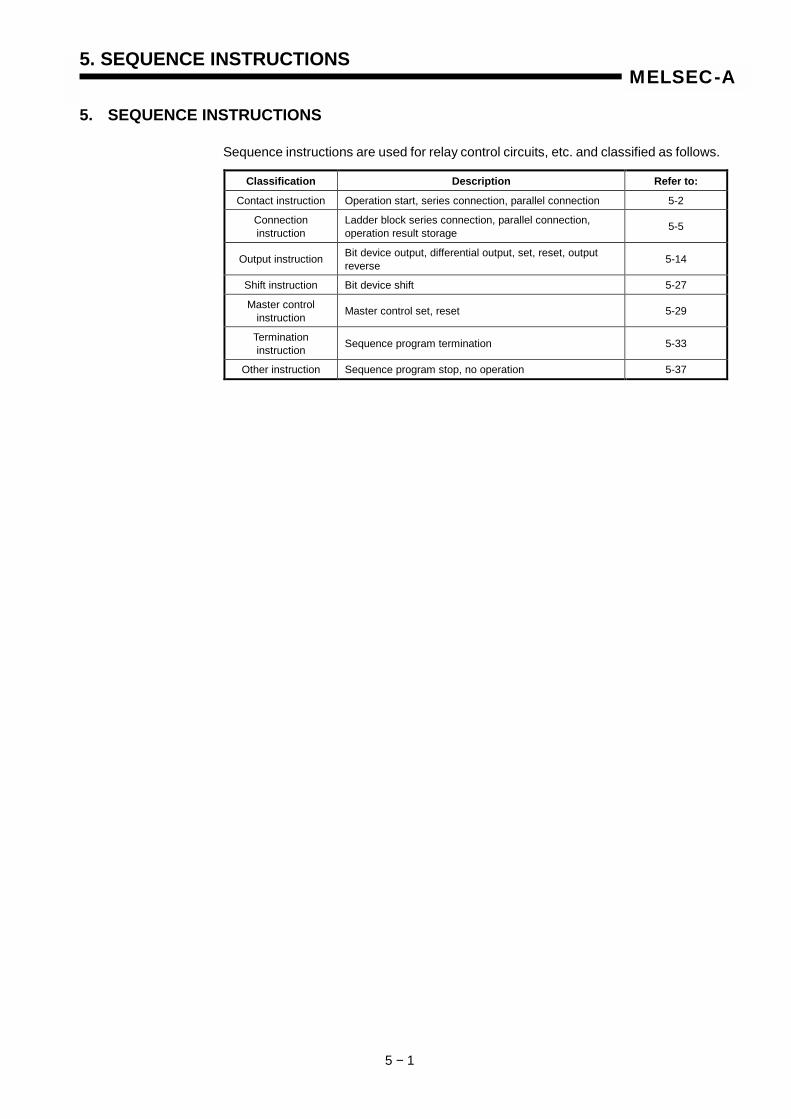
5. SEQUENCE INSTRUCTIONS
5 − 1
MELSEC-A
5. SEQUENCE INSTRUCTIONS
Sequence instructions are used for relay control circuits, etc. and classified as follows.
Classification Description Refer to:
Contact instruction Operation start, series connection, parallel connection 5-2
Connection instruction
Ladder block series connection, parallel connection, operation result storage 5-5
Output instruction Bit device output, differential output, set, reset, output reverse 5-14
Shift instruction Bit device shift 5-27
Master control instruction Master control set, reset 5-29
Termination instruction Sequence program termination 5-33
Other instruction Sequence program stop, no operation 5-37
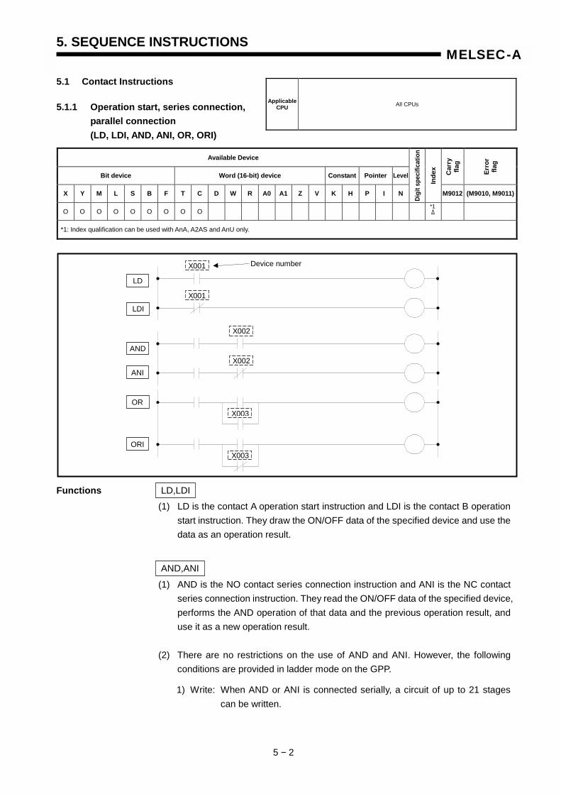
5. SEQUENCE INSTRUCTIONS
5 − 2
MELSEC-A
5.1 Contact Instructions
5.1.1 Operation start, series connection, parallel connection (LD, LDI, AND, ANI, OR, ORI)
Available Device
Bit device Word (16-bit) device Constant Pointer Level Car
ry
flag
Erro
r fla
g
X Y M L S B F T C D W R A0 A1 Z V K H P I N
Digi
t spe
cific
atio
n
Inde
x
M9012 (M9010, M9011)
O O O O O O O O O
*1: Index qualification can be used with AnA, A2AS and AnU only.
Functions LD,LDI (1) LD is the contact A operation start instruction and LDI is the contact B operation
start instruction. They draw the ON/OFF data of the specified device and use the data as an operation result.
AND,ANI
(1) AND is the NO contact series connection instruction and ANI is the NC contact series connection instruction. They read the ON/OFF data of the specified device, performs the AND operation of that data and the previous operation result, and use it as a new operation result.
(2) There are no restrictions on the use of AND and ANI. However, the following
conditions are provided in ladder mode on the GPP.
1) Write: When AND or ANI is connected serially, a circuit of up to 21 stages can be written.
Applicable CPU All CPUs
LD
LDI
AND
ANI
OR
ORI
X001
X003
X001
X002
X002
X003
Device number
*1
5. SEQUENCE INSTRUCTIONS
5 − 3
MELSEC-A
2) Read: When AND or ANI is connected serially, a circuit of up to 24 stages can be displayed at one time. if a circuit has 25 or more stages, stages 1to 24 are displayed at one time.
OR, ORI (1) OR is the parallel connection instruction of one contact A and ORI is the parallel
connection instruction of one contact B. They draw the ON/OFF data of the specified device, performs the OR operation of that data and the previous operation result, and use it as a new operation result.
(2) There are no restrictions on the use of OR and ORI. However, the following
conditions are provided in ladder mode on the GPP. 1) Write: A circuit, in which up to 23 ORs or ORIs are connected consecutively,
may be written. 2) Read: A circuit, in which up to 23 ORs or ORIs are connected consecutively,
may be displayed. A circuit containing more than 23 ORs or ORIs cannot be completely displayed.
Execution Executed every scan independently of the device status and operation result. Conditions
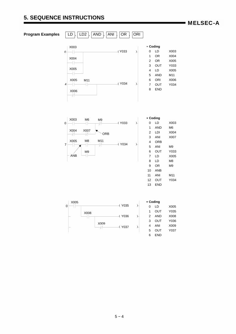
5. SEQUENCE INSTRUCTIONS
5 − 4
MELSEC-A
Program Examples LD , LD2 , AND , ANI , OR , ORI
• Coding 0 LD X003 1 OR X004 2 OR X005 3 OUT Y033 4 LD X005 5 AND M11 6 ORI X006 7 OUT Y034 8 END
( )
( )X003
X004
X005
X005
X006
M11
Y033
Y034
0
4
•••• Coding 0 LD X003 1 AND M6 2 LDI X004 3 ANI X007 4 ORB 5 ANI M9 6 OUT Y033 7 LD X005 8 LD M8 9 OR M9 10 ANB 11 ANI M11 12 OUT Y034 13 END
( )
( )
X003
X004
X005
M6
X007
M8
M9
M9
M11
Y033
Y034
0
7
ANB
ORB
•••• Coding 0 LD X005 1 OUT Y035 2 AND X008 3 OUT Y036 4 ANI X009 5 OUT Y037 6 END
( )
( )
( )
X005
X008
X009
Y035
Y036
Y037
0

5. SEQUENCE INSTRUCTIONS
5 − 5
MELSEC-A
5.2 Connection Instructions
5.2.1 Ladder block series connection, parallel connection (ANB, ORB)
Available Device
Bit device Word (16-bit) device Constant Pointer Level Car
ry
flag
Erro
r fla
g
X Y M L S B F T C D W R A0 A1 Z V K H P I N Digi
t spe
cific
atio
n
Inde
x
M9012 (M9010, M9011)
Functions ANB (1) This instruction performs the AND operation of block A and Block B, and uses it
as an operation result. (2) The symbol of ANB is not a contact symbol but a connection symbol. (3) ANB can be written consecutively up to the number of instructions mentioned
below. For AnA, A2AS and AnU : 15 instructions (16 blocks) For CPUs other than AnA, A2AS and AnU : 7 instructions (8 blocks) If more ANBs are written consecutively, the PC cannot perform proper opera-tion.
Applicable CPU All CPUs
ANB
Block A Block B
ORB
Block A
Block B For the parallel connection of one contact, use OR or ORI.
ANB
ORB
5. SEQUENCE INSTRUCTIONS
5 − 6
MELSEC-A
ORB (1) This instruction performs the OR operation of block A and block B, and uses it as
an operation result. (2) ORB performs parallel connection of circuit blocks with two or more contacts. For
parallel connection of circuit blocks which have only one contact, OR and ORI are used and ORB is not required. (See below.)
(3) The symbol of ORB is not a contact symbol but a connection symbol. (4) ORB can be written consecutively up to the number of instructions mentioned
below. For AnA, A2AS and AnU : 15 instructions (16 blocks) For CPUs other than AnA, A2AS and AnU : 7 instructions (8 blocks) If more ORBs are written consecutively, the PC cannot perform proper
opera-tion.
( )
•••• Coding 0 LD X000 1 AND X001 2 LD X002 3 AND X003 4 ORB 5 OR X004 6 OUT Y010 7 END
X001 X000
X003 X002
Y010
X004
0
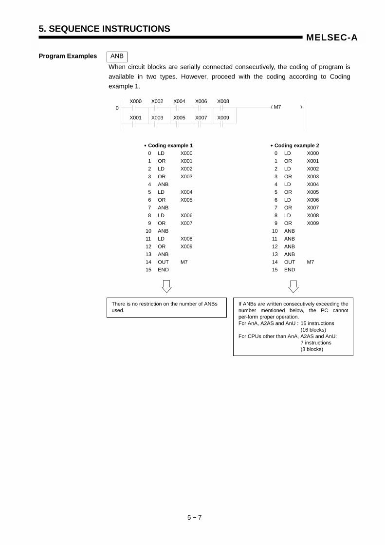
5. SEQUENCE INSTRUCTIONS
5 − 7
MELSEC-A
Program Examples ANB When circuit blocks are serially connected consecutively, the coding of program is available in two types. However, proceed with the coding according to Coding example 1.
( )X002 X000
X003 X001
0 X006 X004
X007 X005
X008
X009
M7
•••• Coding example 1 0 LD X000 1 OR X001 2 LD X002 3 OR X003 4 ANB 5 LD X004 6 OR X005 7 ANB 8 LD X006 9 OR X007 10 ANB 11 LD X008 12 OR X009 13 ANB 14 OUT M7 15 END
•••• Coding example 2 0 LD X000 1 OR X001 2 LD X002 3 OR X003 4 LD X004 5 OR X005 6 LD X006 7 OR X007 8 LD X008 9 OR X009 10 ANB 11 ANB 12 ANB 13 ANB 14 OUT M7 15 END
There is no restriction on the number of ANBs used.
If ANBs are written consecutively exceeding thenumber mentioned below, the PC cannotper-form proper operation. For AnA, A2AS and AnU : 15 instructions (16 blocks) For CPUs other than AnA, A2AS and AnU: 7 instructions (8 blocks)
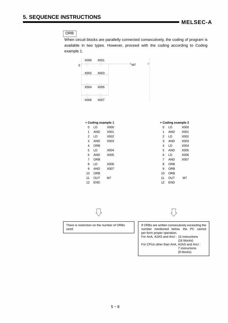
5. SEQUENCE INSTRUCTIONS
5 − 8
MELSEC-A
ORB When circuit blocks are parallelly connected consecutively, the coding of program is available in two types. However, proceed with the coding according to Coding example 1.
( )X001 X000
X003 X002
M7 0
X005 X004
X007 X006
•••• Coding example 1 0 LD X000 1 AND X001 2 LD X002 3 AND X003 4 ORB 5 LD X004 6 AND X005 7 ORB 8 LD X006 9 AND X007 10 ORB 11 OUT M7 12 END
•••• Coding example 2 0 LD X000 1 AND X001 2 LD X002 3 AND X003 4 LD X004 5 AND X005 6 LD X006 7 AND X007 8 ORB 9 ORB 10 ORB 11 OUT M7 12 END
There is restriction on the number of ORBs used.
If ORBs are written consecutively exceeding thenumber mentioned below, the PC cannotper-form proper operation. For AnA, A2AS and AnU : 15 instructions (16 blocks) For CPUs other than AnA, A2AS and AnU : 7 instructions (8 blocks)
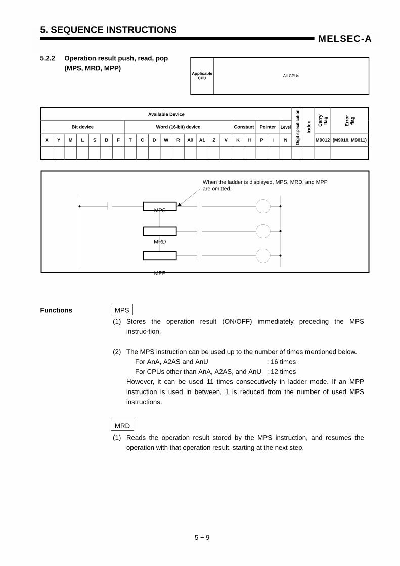
5. SEQUENCE INSTRUCTIONS
5 − 9
MELSEC-A
5.2.2 Operation result push, read, pop (MPS, MRD, MPP)
Available Device
Bit device Word (16-bit) device Constant Pointer Level Car
ry
flag
Erro
r fla
g
X Y M L S B F T C D W R A0 A1 Z V K H P I N Digi
t spe
cific
atio
n
Inde
x
M9012 (M9010, M9011)
Functions MPS (1) Stores the operation result (ON/OFF) immediately preceding the MPS
instruc-tion. (2) The MPS instruction can be used up to the number of times mentioned below. For AnA, A2AS and AnU : 16 times For CPUs other than AnA, A2AS, and AnU : 12 times However, it can be used 11 times consecutively in ladder mode. If an MPP
instruction is used in between, 1 is reduced from the number of used MPS instructions.
MRD
(1) Reads the operation result stored by the MPS instruction, and resumes the operation with that operation result, starting at the next step.
Applicable CPU All CPUs
MPS
MRD
MPP
When the ladder is dispiayed, MPS, MRD, and MPP are omitted.
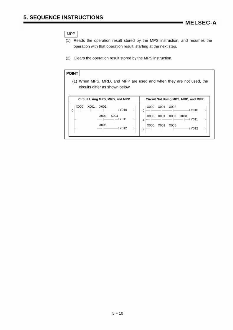
5. SEQUENCE INSTRUCTIONS
5 − 10
MELSEC-A
MPP (1) Reads the operation result stored by the MPS instruction, and resumes the
operation with that operation result, starting at the next step. (2) Clears the operation result stored by the MPS instruction.
POINT
(1) When MPS, MRD, and MPP are used and when they are not used, the circuits differ as shown below.
Circuit Using MPS, MRD, and MPP Circuit Not Using MPS, MRD, and MPP
( )
( )
( )
( )
( )
( )
0 X000 X001 X002
X005
X003 X004
Y010
Y012
Y011
0 X000 X001 X002
4 X000 X001 X003
9 X000 X001 X005
X004
Y010
Y012
Y011
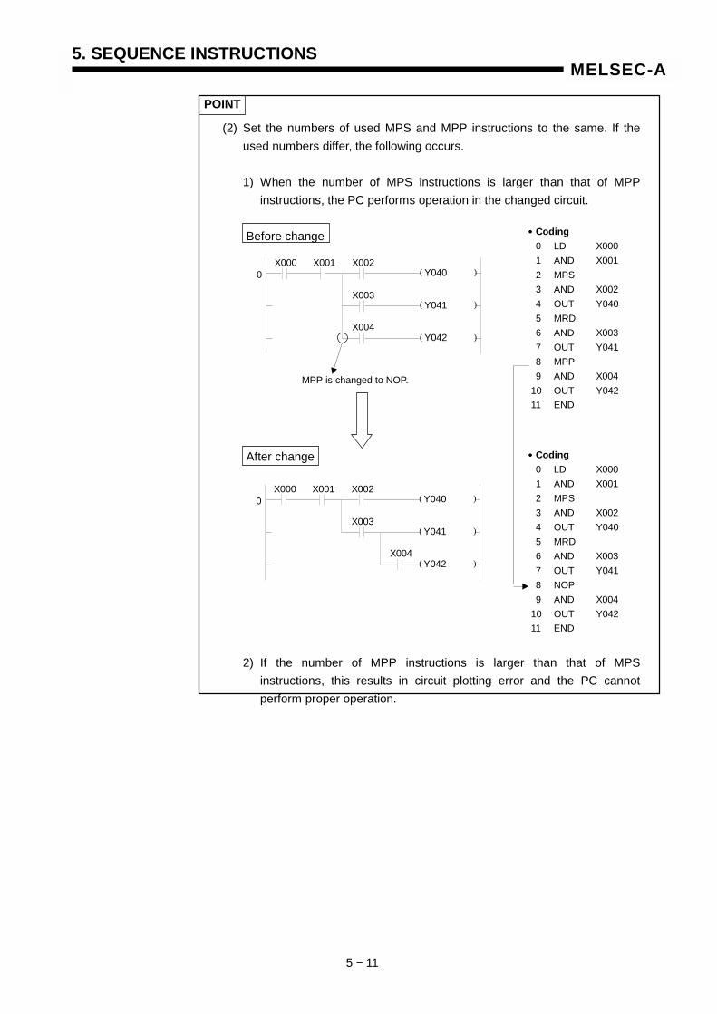
5. SEQUENCE INSTRUCTIONS
5 − 11
MELSEC-A
POINT
(2) Set the numbers of used MPS and MPP instructions to the same. If the used numbers differ, the following occurs.
1) When the number of MPS instructions is larger than that of MPP
instructions, the PC performs operation in the changed circuit. Before change
After change
2) If the number of MPP instructions is larger than that of MPS instructions, this results in circuit plotting error and the PC cannot perform proper operation.
•••• Coding 0 LD X000 1 AND X001 2 MPS 3 AND X002 4 OUT Y040 5 MRD 6 AND X003 7 OUT Y041 8 MPP 9 AND X004 10 OUT Y042 11 END
•••• Coding 0 LD X000 1 AND X001 2 MPS 3 AND X002 4 OUT Y040 5 MRD 6 AND X003 7 OUT Y041 8 NOP 9 AND X004 10 OUT Y042 11 END
( )
( )
( )
0 X000 X001 X002
X004
X003
Y040
Y042
Y041
MPP is changed to NOP.
( )
( )
( )
0 X000 X001 X002
X004
X003
Y040
Y042
Y041
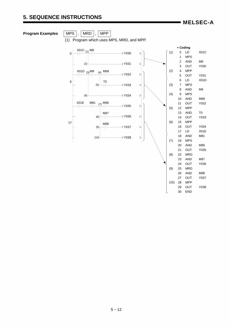
5. SEQUENCE INSTRUCTIONS
5 − 12
MELSEC-A
Program Examples MPS , MRD , MPP (1) Program which uses MPS, MRD, and MPP.
•••• Coding 0 LD X01C 1 MPS 2 AND M8 3 OUT Y030 4 MPP 5 OUT Y031 6 LD X01D 7 MPS 8 AND M9 9 MPS 10 AND M68 11 OUT Y032 12 MPP 13 AND T0 14 OUT Y033 15 MPP 16 OUT Y034 17 LD X01E 18 AND M81 19 MPS 20 AND M96 21 OUT Y035 22 MRD 23 AND M97 24 OUT Y036 25 MRD 26 AND M98 27 OUT Y037 28 MPP 29 OUT Y038 30 END
( )
( )
( )
( )
( )
( )
( )
( )
( )
0 X01C M8
X01D M68 M9
Y030
Y032
Y031
T0 Y033
Y035
Y034
Y036
Y038
Y037
X01E M96 M81
M97
M98
(1) (2) (3) (4) (5) (6) (7) (8) (9) (10)
(1)
(2)
(3) (4)
(6)
(5)
(7)
(8)
(9)
(10)
6
17
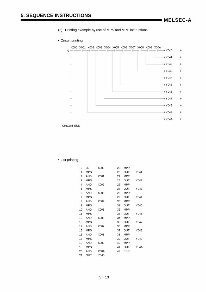
5. SEQUENCE INSTRUCTIONS
5 − 13
MELSEC-A
(2) Printing example by use of MPS and MPP instructions. • Circuit printing
• List printing
( )
( )
( )
( )
( )
( )
( )
( )
( )
( )
( )
0 X000 X001 X002 X004 X003
Y040
Y042
Y041
Y043
Y045
Y044
Y046
Y048
Y047
Y049
Y04A
X005 X006 X007 X009 X008 X00A
CIRCUIT END
0 LD X000 1 MPS 2 AND X001 3 MPS 4 AND X002 5 MPS 6 AND X003 7 MPS 8 AND X004 9 MPS 10 AND X005 11 MPS 12 AND X006 13 MPS 14 AND X007 15 MPS 16 AND X008 17 MPS 18 AND X009 19 MPS 20 AND X00A 21 OUT Y040
22 MPP 23 OUT Y041 24 MPP 25 OUT Y042 26 MPP 27 OUT Y043 28 MPP 29 OUT Y044 30 MPP 31 OUT Y045 32 MPP 33 OUT Y046 34 MPP 35 OUT Y047 36 MPP 37 OUT Y048 38 MPP 39 OUT Y049 40 MPP 41 OUT Y04A 42 END
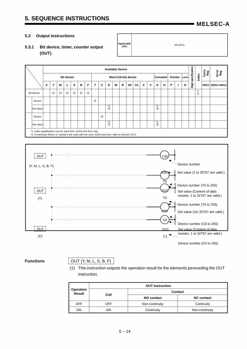
5. SEQUENCE INSTRUCTIONS
5 − 14
MELSEC-A
5.3 Output Instructions
5.3.1 Bit device, timer, counter output (OUT)
Available Device
Bit device Word (16-bit) device Constant Pointer Level Car
ry
flag
Erro
r fla
g
X Y M L S B F T C D W R A0 A1 Z V K H P I N Digi
t spe
cific
atio
n
Inde
x
M9012 (M9010, M9011)
Bit device O O O O O O
Device O
Set Value O O
Device O
Set value O O
*1: Index qualification can be used AnA, A2AS and AnU only. *2: If extension timers or counters are used with the AnA, A2AS and AnU, refer to Section 3.8.3.
Functions OUT (Y, M, L, S, B, F) (1) This instruction outputs the operation result for the elements pereceding the OUT
instruction.
OUT Instruction
Contact Operation Result Coil
NO contact NC contact
OFF OFF Non-continuity Continuity
ON ON Continuity Non-continuity
Applicable CPU All CPUs
*2
*2
*2
*2
*1
OUT
OUT
OUT
(Y, M, L, S, B, F)
(T)
(C)
Y35
Device number
T0
Set value (Content of data resister. 1 to 32767 are valid.)
K50 Set value (1 to 32767 are valid.)
Set value (1to 32767 are valid.)
Device number (T0 to 255) D10
Device number (T0 to 255)
T0
K50
Set value (Content of data resister. 1 to 32767 are valid.)
C0 Device number (C0 to 255)
D10
C1
Device number (C0 to 255)
5. SEQUENCE INSTRUCTIONS
5 − 15
MELSEC-A
POINTS
(1) When F (annunciator) is turned ON, LED indicators and ERROR LEDs on the CPU module illuminate, and the number of annunciator which is turned ON is stored in special registers. For details, refer to the ACPU Programming Manual (Fundamentals).
(2) If the OUT instruction is used to turn ON the annunciator, annunciator coil status does not correspond to the display of LED indicators. To avoid this, use the SET instruction to turn ON the annunciator. If the OUT instruction is used to turn ON the annunciator, the annunciator coil turns OFF when the operation result of instructions preceding the OUT instruction turns OFF. However, display contents of LED indicators and ERROR LEDs on the CPU module and contents of special registers do not change. For details, refer to the ACPU Programming Manual (Fundamentals).
REMARK
The number of steps is 3 when either of the following devices is used for OUT instruction: • Special relay (M) • Annunciator (F)
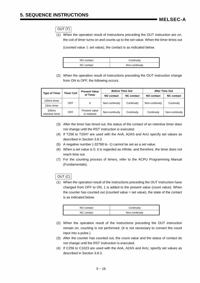
5. SEQUENCE INSTRUCTIONS
5 − 16
MELSEC-A
OUT (T) (1) When the operation result of instructions preceding the OUT instruction are on,
the coil of timer turns on and counts up to the set value. When the timer times out
(counted value ≧ set value), the contact is as indicated below.
NO contact Continuity
NC contact Non-continuity
(2) When the operation result of instructions preceding the OUT instruction change from ON to OFF, the following occurs.
Before TIme Out After Time Out
Type of Timer Timer Coil Present Value of Timer NO contact NC contact NO contact NC contact
100ms timer
10ms timer OFF 0 Non-continuity Continuity Non-continuity Coninuity
100ms retentive timer OFF Present value
is retained Non-continuity Continuity Continuity Non-continuity
(3) After the timer has timed out, the status of the contact of an retentive timer does not change until the RST instruction is executed.
(4) If T256 to T2047 are used with the AnA, A2AS and AnU specify set values as described in Section 3.8.3.
(5) A negative number (-32768 to -1) cannot be set as a set value. (6) When a set value is 0, it is regarded as infinite, and therefore, the timer does not
reach time out. (7) For the counting process of timers, refer to the ACPU Programming Manual
(Fundamentals).
OUT (C) (1) When the operation result of the instructions preceding the OUT instruction have
changed from OFF to ON, 1 is added to the present value (count value). When the counter has counted out (counted value = set value), the state of the contact is as indicated below.
NO contact Continuity
NC contact Non-continuity
(2) When the operation result of the instructions preceding the OUT instruction remain on, counting is not performed. (It is not necessary to convert the count input into a pulse.)
(3) After the counter has counted out, the count value and the status of contact do not change until the RST instruction is executed.
(4) If C256 to C1023 are used with the AnA, A2AS and AnU, specify set values as described in Section 3.8.3.
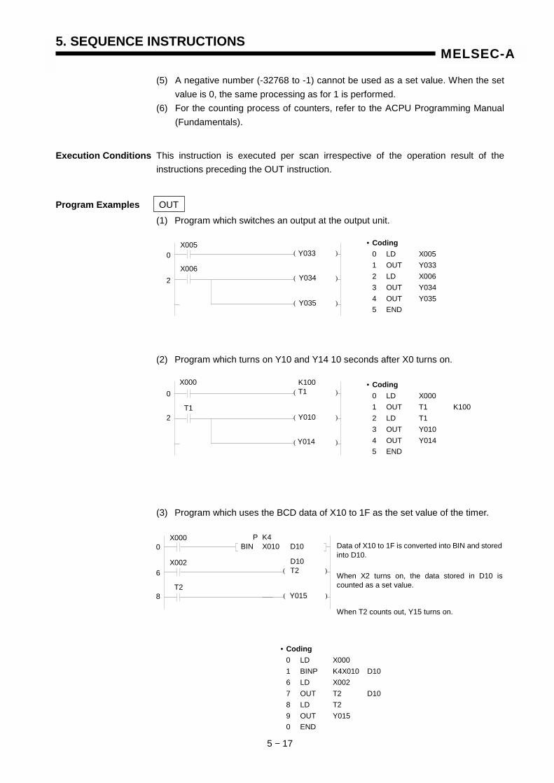
5. SEQUENCE INSTRUCTIONS
5 − 17
MELSEC-A
(5) A negative number (-32768 to -1) cannot be used as a set value. When the set value is 0, the same processing as for 1 is performed.
(6) For the counting process of counters, refer to the ACPU Programming Manual (Fundamentals).
Execution Conditions This instruction is executed per scan irrespective of the operation result of the instructions preceding the OUT instruction.
Program Examples OUT (1) Program which switches an output at the output unit.
(2) Program which turns on Y10 and Y14 10 seconds after X0 turns on.
(3) Program which uses the BCD data of X10 to 1F as the set value of the timer.
• Coding 0 LD X005 1 OUT Y033 2 LD X006 3 OUT Y034 4 OUT Y035 5 END
• Coding 0 LD X000 1 OUT T1 K100 2 LD T1 3 OUT Y010 4 OUT Y014 5 END
( )
( )
( )
X005
X006
Y033
Y034
Y035
0
2
X000 ( )
( )
( )
T1
K100 T1
Y010
Y014
0
2
Data of X10 to 1F is converted into BIN and stored into D10.
( )
( )
0
6
8 Y015
X000
X002
T2
P K4 BIN X010 D10
D10 T2
• Coding 0 LD X000 1 BINP K4X010 D10 6 LD X002 7 OUT T2 D10 8 LD T2 9 OUT Y015 0 END
When T2 counts out, Y15 turns on.
When X2 turns on, the data stored in D10 iscounted as a set value.
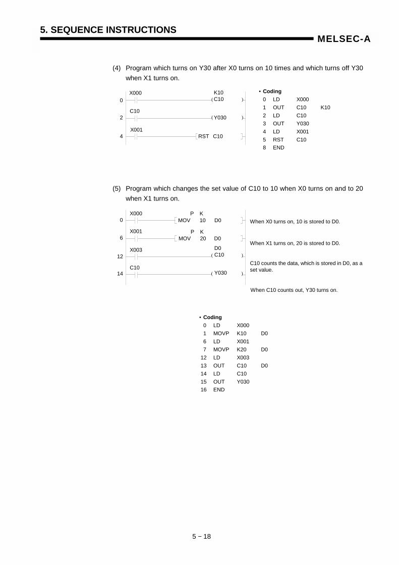
5. SEQUENCE INSTRUCTIONS
5 − 18
MELSEC-A
(4) Program which turns on Y30 after X0 turns on 10 times and which turns off Y30 when X1 turns on.
(5) Program which changes the set value of C10 to 10 when X0 turns on and to 20 when X1 turns on.
( )
( )
0
2
4 X001
X000
C10
K10 C10
Y030
RST C10
• Coding 0 LD X000 1 OUT C10 K10 2 LD C10 3 OUT Y030 4 LD X001 5 RST C10 8 END
When X1 turns on, 20 is stored to D0.
When X0 turns on, 10 is stored to D0.
( )
( )
0
6
12
14 C10
X000
X001
X003
P K MOV 10 D0
Y030
D0 C10
P K MOV 20 D0
C10 counts the data, which is stored in D0, as aset value.
When C10 counts out, Y30 turns on.
• Coding 0 LD X000 1 MOVP K10 D0 6 LD X001 7 MOVP K20 D0 12 LD X003 13 OUT C10 D0 14 LD C10 15 OUT Y030 16 END
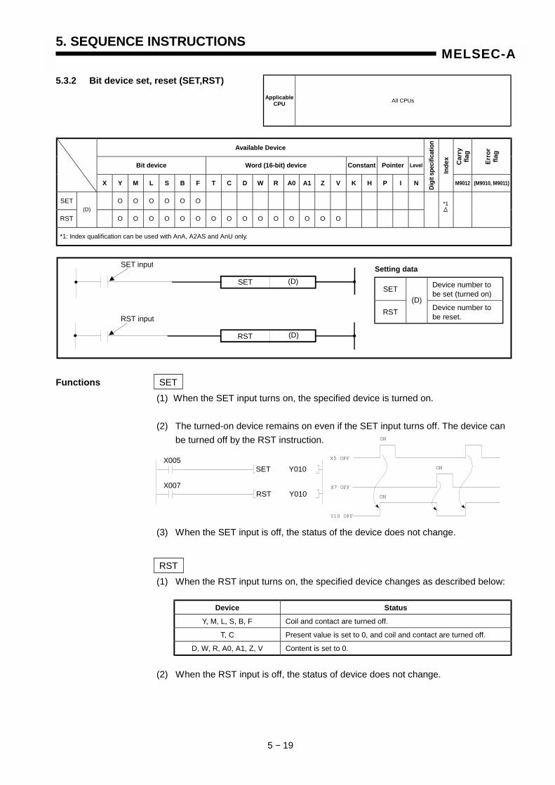
5. SEQUENCE INSTRUCTIONS
5 − 19
MELSEC-A
5.3.2 Bit device set, reset (SET,RST)
Available Device
Bit device Word (16-bit) device Constant Pointer Level Car
ry
flag
Erro
r fla
g
X Y M L S B F T C D W R A0 A1 Z V K H P I N Digi
t spe
cific
atio
n
Inde
x
M9012 (M9010, M9011)
SET O O O O O O
RST (D)
O O O O O O O O O O O O O O O
*1: Index qualification can be used with AnA, A2AS and AnU only.
Functions SET (1) When the SET input turns on, the specified device is turned on. (2) The turned-on device remains on even if the SET input turns off. The device can
be turned off by the RST instruction.
(3) When the SET input is off, the status of the device does not change.
RST (1) When the RST input turns on, the specified device changes as described below:
Device Status
Y, M, L, S, B, F Coil and contact are turned off.
T, C Present value is set to 0, and coil and contact are turned off.
D, W, R, A0, A1, Z, V Content is set to 0.
(2) When the RST input is off, the status of device does not change.
Applicable CPU All CPUs
*1
X5 OFF
X7 OFF
Y10 OFF
ON
ON
ON
X005
X007
SET Y010
RST Y010
SET Device number to be set (turned on)
RST (D)
Device number to be reset.
Setting data SET input
RST input
SET
RST
(D)
(D)

5. SEQUENCE INSTRUCTIONS
5 − 20
MELSEC-A
(3) The functions of RST (D, W, R, A0, A1, Z, V) are the same as those of the following circuit.
If the annunciator relay (F ) is turned ON/OFF, display contents of LED indicators and ERROR LEDs on the CPU module and contents of special registers change. For details, refer to the ACPU Programming Manual (Fundamentals).
Execution (1) The SET, RST instructions are executed on the following conditions: Conditions
(2) SET, RST instructions In refresh mode, the SET/RST instructions cannot be used in a program which
outputs a pulse signal during one scan. In this case, output (Y) must be changed to direct mode or the program must be corrected so that the device is switched on/off every scan as shown below.
REMARK
The number of steps is 3 when any of the following devices is used: SET instruction Special relay (M) Link relay (B) Annunciator (F) RST instruction Special relay (M) Word devices (All)
RST input RST input
Device number (D, W, R, A0, A1, Z, V)
Device number (D, W, R, A0, A1, Z, V)
X010 RST D50
X010 K MOV 0 D50
X000 SET Y010
RST Y010
( )
X000 M0
M0
M0
SET Y010
RST Y010
M0
Direct mode Refresh mode
SET, RST instruction
SET, RST (Y, M, L, S, B)
SET, RST (F)
OFF
ON
Executed every scan Executed ever scan
Executed only once
Executed only once
ON
OFF
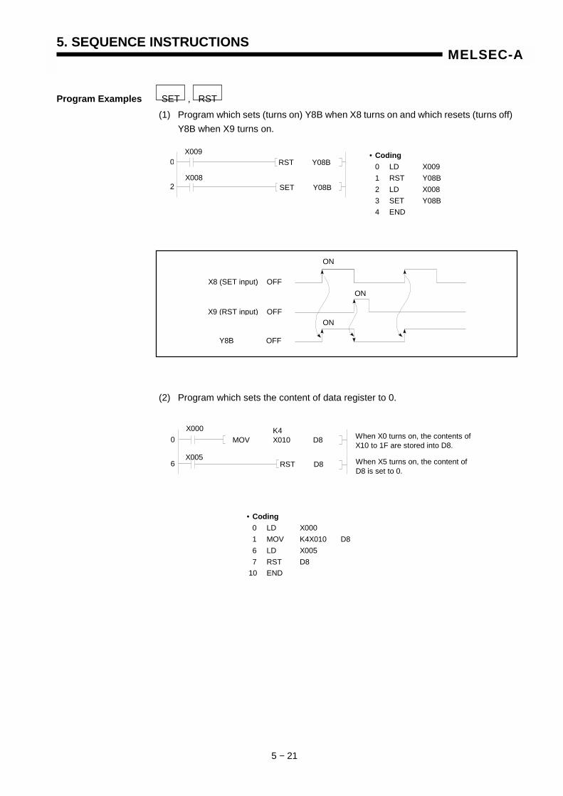
5. SEQUENCE INSTRUCTIONS
5 − 21
MELSEC-A
Program Examples SET , RST (1) Program which sets (turns on) Y8B when X8 turns on and which resets (turns off)
Y8B when X9 turns on. (2) Program which sets the content of data register to 0.
• Coding 0 LD X000 1 MOV K4X010 D8 6 LD X005 7 RST D8 10 END
When X0 turns on, the contents of X10 to 1F are stored into D8.
When X5 turns on, the content of D8 is set to 0.
K4 MOV X010 D8
RST D8
0
6
• Coding 0 LD X009 1 RST Y08B 2 LD X008 3 SET Y08B 4 END
X009
X008
RST Y08B
SET Y08B
0
2
X8 (SET input) OFF
X9 (RST input) OFF
Y8B OFF
ON
ON
ON
X000
X005
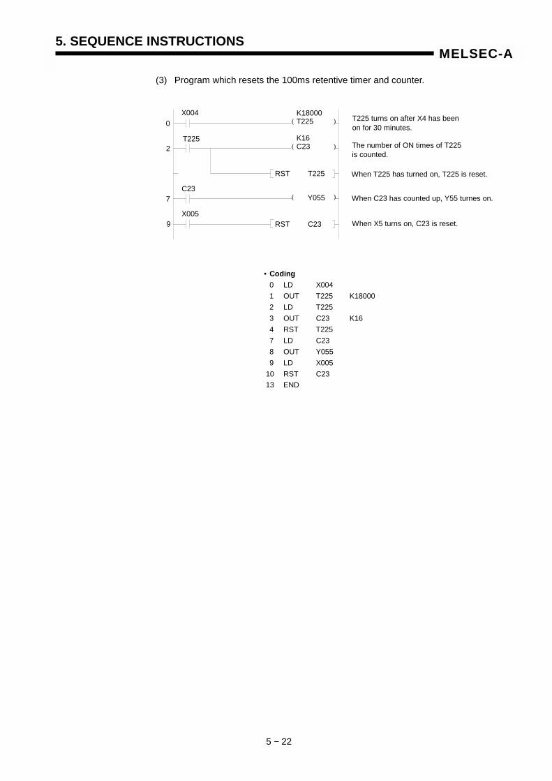
5. SEQUENCE INSTRUCTIONS
5 − 22
MELSEC-A
(3) Program which resets the 100ms retentive timer and counter.
• Coding 0 LD X004 1 OUT T225 K18000 2 LD T225 3 OUT C23 K16 4 RST T225 7 LD C23 8 OUT Y055 9 LD X005 10 RST C23 13 END
( )
( )
( ) T225 turns on after X4 has been on for 30 minutes.
The number of ON times of T225 is counted.
When T225 has turned on, T225 is reset.
When C23 has counted up, Y55 turnes on.
When X5 turns on, C23 is reset.
X004
T225
C23
X005
K18000 T225
K16 C23
RST T225
RST C23
Y055
0
2
7
9

5. SEQUENCE INSTRUCTIONS
5 − 23
MELSEC-A
5.3.3 Edge-triggered differential output (PLS, PLF)
Available Device
Bit device Word (16-bit) device Constant Pointer Level Car
ry
flag
Erro
r fla
g
X Y M L S B F T C D W R A0 A1 Z V K H P I N Digi
t spe
cific
atio
n
Inde
x
M9012 (M9010, M9011)
(D) O O O O O O
*1: Index qualification can be used with AnA, A2AS and AnU only.
Function PLS (1) The PLS instruction turns on the specified device for one scan when the PLS
instruction turns from off to on. Similarly, when a device is in the on state, the PLS instruction will turn it off for one scan time.
(2) If the instruction generating the pulse is switched on and the RUN key switch is moved from the RUN to STOP position and the RUN key switch is moved from the RUN to STOP position and then returned to the RUN position again, the PLS instruction is not executed.
PLS command
X005 PLS M0
X000 PLS M0
Move RUN key switch of CPU unit from RUN to STOP position
Move RUN key switch of CPU unit from STOP to RUN position
PLS
PLS
PLS command
M0 OFF
X5 OFF
ON
ON
1 scan
Applicable CPU All CPUs
PLF command
(D)
(D)
(D) Device number to be con- verted into pulse
Setting data
X0 OFF
M0 OFF
ON
PLS M0 LDX0
END 0 END PLS M0 LDX0
END PLS M0 LDX0
0
ON
1scan of PLS M0
Operation stop time of PC
Operation stop time of PC
1 scan
*1
5. SEQUENCE INSTRUCTIONS
5 − 24
MELSEC-A
(3) When the latch relay (L) is used with the PLS instruction, the previous data isre-output after the power is restored.
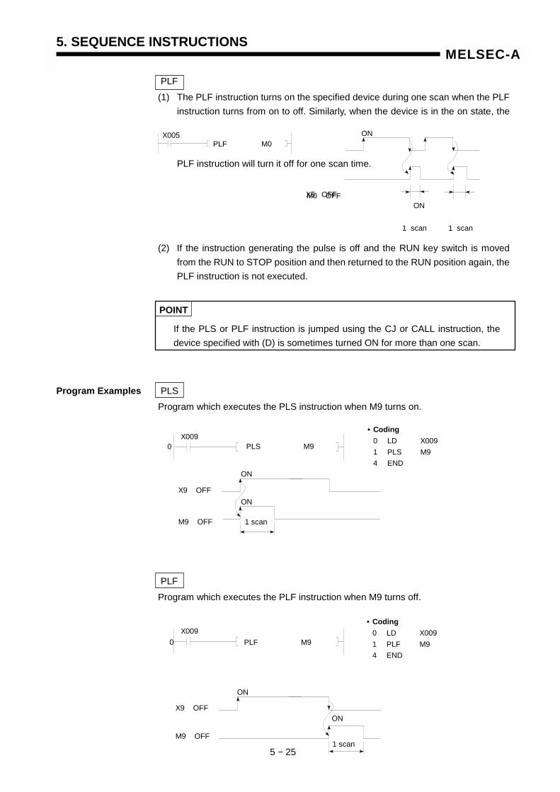
5. SEQUENCE INSTRUCTIONS
5 − 25
MELSEC-A
PLF (1) The PLF instruction turns on the specified device during one scan when the PLF
instruction turns from on to off. Similarly, when the device is in the on state, the
PLF instruction will turn it off for one scan time.
(2) If the instruction generating the pulse is off and the RUN key switch is moved from the RUN to STOP position and then returned to the RUN position again, the PLF instruction is not executed.
POINT
If the PLS or PLF instruction is jumped using the CJ or CALL instruction, the device specified with (D) is sometimes turned ON for more than one scan.
Program Examples PLS Program which executes the PLS instruction when M9 turns on.
PLF Program which executes the PLF instruction when M9 turns off.
X005 PLF M0
• Coding 0 LD X009 1 PLS M9 4 END
ON
X9 OFF
M9 OFF
ON
1 scan
• Coding 0 LD X009 1 PLF M9 4 END
X5 OFF M0 OFF
ON
ON
1 scan 1 scan
X009 PLS M9 0
X009 PLF M9 0
M9 OFF
ON
1 scan
ON
X9 OFF
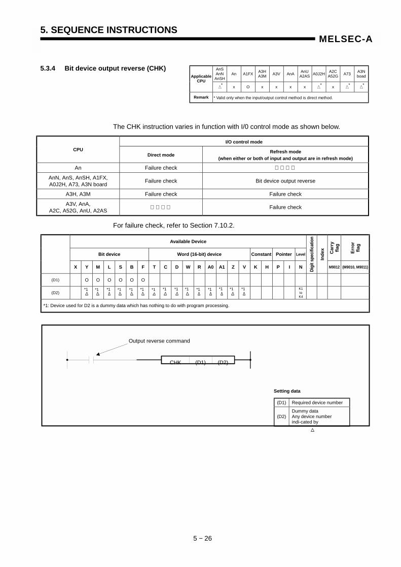
5. SEQUENCE INSTRUCTIONS
5 − 26
MELSEC-A
5.3.4 Bit device output reverse (CHK)
The CHK instruction varies in function with I/0 control mode as shown below.
I/O control mode CPU
Direct mode Refresh mode (when either or both of input and output are in refresh mode)
An Failure check
AnN, AnS, AnSH, A1FX, A0J2H, A73, A3N board Failure check Bit device output reverse
A3H, A3M Failure check Failure check
A3V, AnA, A2C, A52G, AnU, A2AS Failure check
For failure check, refer to Section 7.10.2.
Available Device
Bit device Word (16-bit) device Constant Pointer Level Car
ry
flag
Erro
r fla
g
X Y M L S B F T C D W R A0 A1 Z V K H P I N Digi
t spe
cific
atio
n
Inde
x
M9012 (M9010, M9011)
(D1) O O O O O O
(D2)
*1: Device used for D2 is a dummy data which has nothing to do with program processing.
AnS AnN
AnSH An A1FX A3H
A3M A3V AnA AnU A2AS A0J2H A2C
A52G A73 A3N boad Applicable
CPU x O x x x x x
Remark * Valid only when the input/output control method is direct method.
*1 *1 *1 *1 *1 *1 *1 *1 *1 *1 *1 *1 *1 *1 *1
Output reverse command
CHK (D1) (D2)
(D1) Required device number
(D2) Dummy data Any device number indi-cated by
K1 to K4
Setting data
* * * *
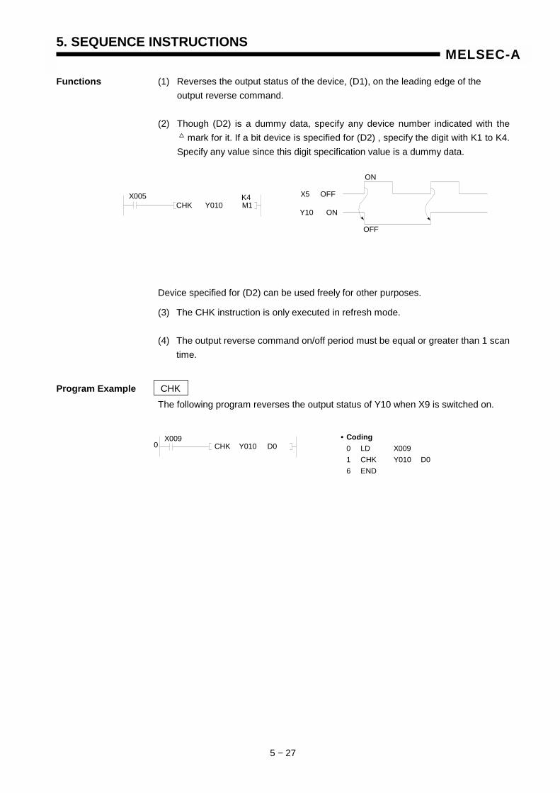
5. SEQUENCE INSTRUCTIONS
5 − 27
MELSEC-A
Functions (1) Reverses the output status of the device, (D1), on the leading edge of the output reverse command.
(2) Though (D2) is a dummy data, specify any device number indicated with the
mark for it. If a bit device is specified for (D2) , specify the digit with K1 to K4. Specify any value since this digit specification value is a dummy data.
Device specified for (D2) can be used freely for other purposes.
(3) The CHK instruction is only executed in refresh mode. (4) The output reverse command on/off period must be equal or greater than 1 scan
time.
Program Example CHK The following program reverses the output status of Y10 when X9 is switched on.
X005 K4 CHK Y010 M1
X5 OFF
Y10 ON
OFF
ON
0 X009
CHK Y010 D0 • Coding 0 LD X009 1 CHK Y010 D0 6 END
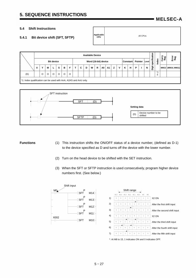
5. SEQUENCE INSTRUCTIONS
5 − 27
MELSEC-A
5.4 Shift Instructions
5.4.1 Bit device shift (SFT, SFTP)
Available Device
Bit device Word (16-bit) device Constant Pointer Level Car
ry
flag
Erro
r fla
g
X Y M L S B F T C D W R A0 A1 Z V K H P I N Digi
t spe
cific
atio
n
Inde
x
M9012 (M9010, M9011)
(D) O O O O O O
*1: Index qualification can be used with AnA, A2AS and AnU only.
Functions (1) This instruction shifts the ON/OFF status of a device number, (defined as D-1) to the device specified as D and turns off the device with the lower number.
(2) Turn on the head device to be shifted with the SET instruction. (3) When the SFT or SFTP instruction is used consecutively, program higher device
numbers first. (See below.)
Setting data
*1
Applicable CPU All CPUs
SFT
SFTP
(D)
(D)
SFT instruction
M15 M14 M13 M12 M11 M10 M9
00 0 0 0 1 1 0
M8
00 1 0 0 0 1 0
00 0 0 1 0 1 0
00 0 1 0 0 1 0
00 0 1 0 1 1 0
00 1 0 1 0 1 0
10 0 1 0 0 1 0
1)
2)
3)
4)
5)
6)
7)
After the second shift input
X2 ON
After the first shift input
X2 ON
After the third shift input
After the fourth shift input
After the fifth shift input
Shift range
*: At M8 to 15, 1 indicates ON and 0 indicates OFF.
Shift input
M0
X002
P SFT M14 P SFT M13 P SFT M12 P SFT M11
SFT M10
(D) Device number to be shifted
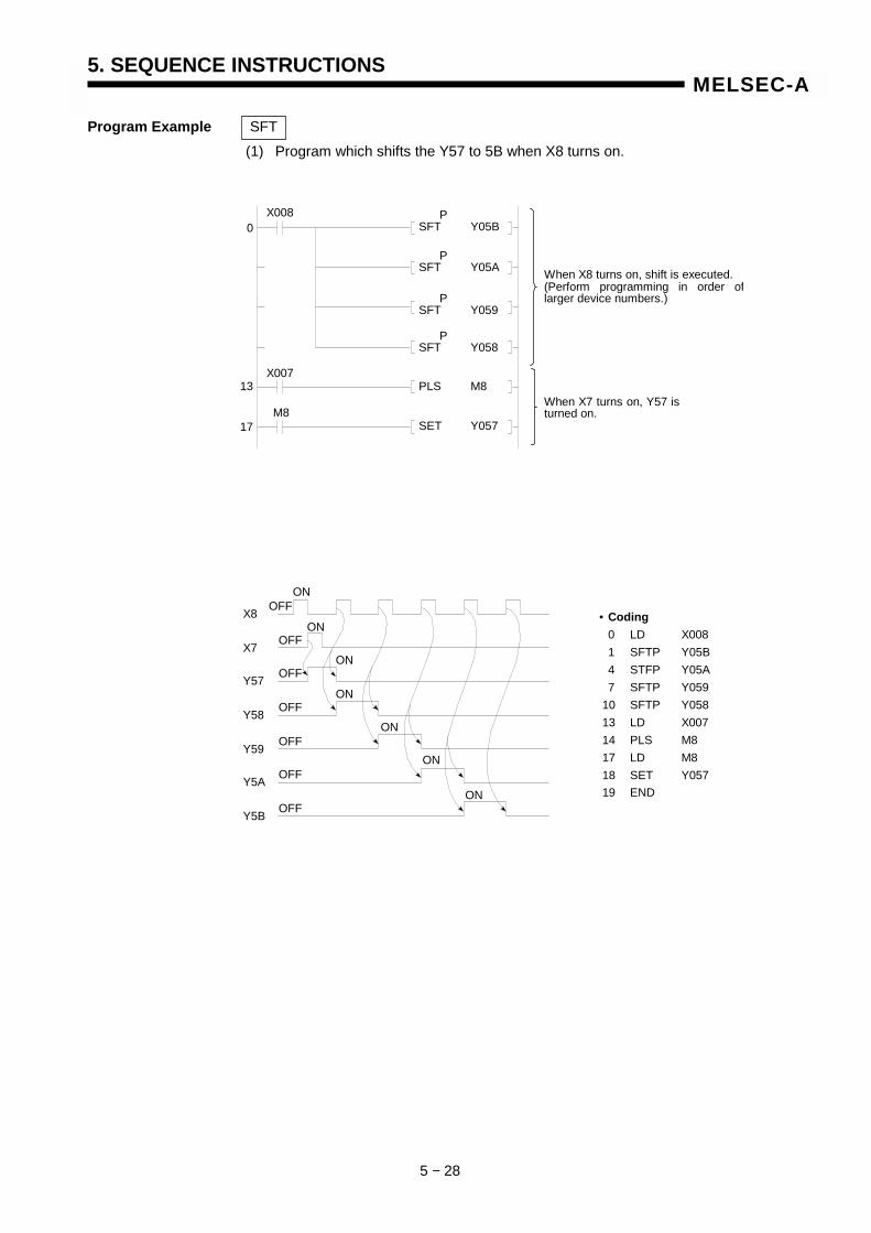
5. SEQUENCE INSTRUCTIONS
5 − 28
MELSEC-A
Program Example SFT (1) Program which shifts the Y57 to 5B when X8 turns on.
OFF X8
X7
Y57
Y58
Y59
Y5A
Y5B
ON
OFF
OFF
OFF
OFF
OFF
OFF
ON
ON
ON
ON
ON
ON
• Coding 0 LD X008 1 SFTP Y05B 4 STFP Y05A 7 SFTP Y059 10 SFTP Y058 13 LD X007 14 PLS M8 17 LD M8 18 SET Y057 19 END
X008 0
P SFT Y05B
P SFT Y05A
P SFT Y059
P SFT Y058
PLS M8
SET Y057
When X8 turns on, shift is executed. (Perform programming in order of larger device numbers.)
When X7 turns on, Y57 isturned on.
13
17
X007
M8
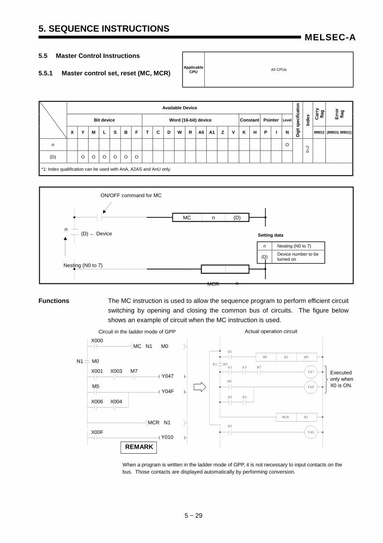
5. SEQUENCE INSTRUCTIONS
5 − 29
MELSEC-A
5.5 Master Control Instructions
5.5.1 Master control set, reset (MC, MCR)
Available Device
Bit device Word (16-bit) device Constant Pointer Level Car
ry
flag
Erro
r fla
g
X Y M L S B F T C D W R A0 A1 Z V K H P I N Digi
t spe
cific
atio
n
Inde
x
M9012 (M9010, M9011)
n O
(D) O O O O O O
*1: Index qualification can be used with AnA, A2AS and AnU only.
Functions The MC instruction is used to allow the sequence program to perform efficient circuit switching by opening and closing the common bus of circuits. The figure below shows an example of circuit when the MC instruction is used.
REMARK
When a program is written in the ladder mode of GPP, it is not necessary to input contacts on the bus. Those contacts are displayed automatically by performing conversion.
*1
Applicable CPU All CPUs
ON/OFF command for MC
MC
MCR
n
n
(D)
n Nesting (N0 to 7)
(D) Device number to be turned on
Setting data (D) ← Device
Nesting (N0 to 7)
n
MC N1 M0
Y47
Y4F
Y40
X0
X1
M5
X6
X3 M7
X4
XF
MCR N1
N1 M0
( )
( )
( )
Circuit in the ladder mode of GPP Actual operation circuit
Executed only when X0 is ON.
X000
N1 M0
MC N1 M0
Y047
Y04F
X001 X003 M7
M5
X006 X004
MCR N1
Y010 X00F
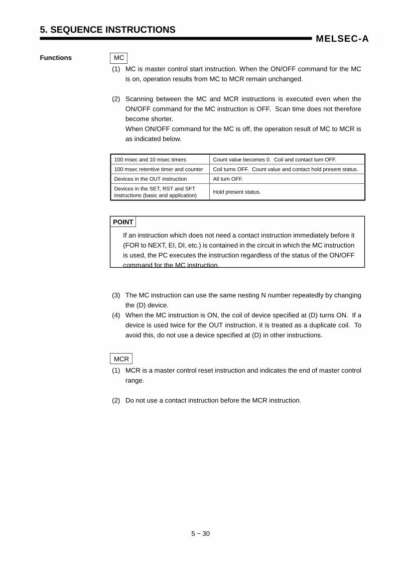
5. SEQUENCE INSTRUCTIONS
5 − 30
MELSEC-A
Functions MC (1) MC is master control start instruction. When the ON/OFF command for the MC is on, operation results from MC to MCR remain unchanged. (2) Scanning between the MC and MCR instructions is executed even when the
ON/OFF command for the MC instruction is OFF. Scan time does not therefore become shorter.
When ON/OFF command for the MC is off, the operation result of MC to MCR is as indicated below.
100 msec and 10 msec timers Count value becomes 0. Coil and contact turn OFF.
100 msec retentive timer and counter Coil turns OFF. Count value and contact hold present status.
Devices in the OUT instruction All turn OFF.
Devices in the SET, RST and SFT instructions (basic and application) Hold present status.
POINT
If an instruction which does not need a contact instruction immediately before it (FOR to NEXT, EI, DI, etc.) is contained in the circuit in which the MC instruction is used, the PC executes the instruction regardless of the status of the ON/OFF command for the MC instruction.
(3) The MC instruction can use the same nesting N number repeatedly by changing the (D) device.
(4) When the MC instruction is ON, the coil of device specified at (D) turns ON. If a device is used twice for the OUT instruction, it is treated as a duplicate coil. To avoid this, do not use a device specified at (D) in other instructions.
MCR (1) MCR is a master control reset instruction and indicates the end of master control
range. (2) Do not use a contact instruction before the MCR instruction.
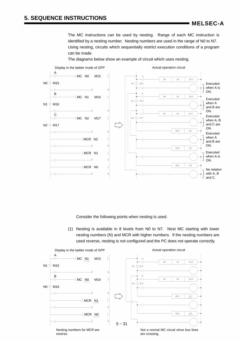
5. SEQUENCE INSTRUCTIONS
5 − 31
MELSEC-A
The MC instructions can be used by nesting. Range of each MC instruction is identified by a nesting number. Nesting numbers are used in the range of N0 to N7. Using nesting, circuits which sequentially restrict execution conditions of a program can be made. The diagrams below show an example of circuit which uses nesting.
Consider the following points when nesting is used. (1) Nesting is available in 8 levels from N0 to N7. Nest MC starting with lower
nesting numbers (N) and MCR with higher numbers. If the nesting numbers are used reverse, nesting is not configured and the PC does not operate correctly.
( )
( )
( )
( )
( )
( )
MC N0 M15
A
M15
B
C
M17
N0
MCR N2
MCR N1
MCR N0
MC N1 M16
MC N2 M17
N1
N2
M16
Display in the ladder mode of GPP Actual operation circuit
Executed when A is ON.
A
N0 M15
MC N0 M15
Executed when A and B are ON. Executed when A, B and C are ON. Executed when A and B are ON.
Executed when A is ON.
No relation with A, B and C.
B
N1 M16
MC N1 M16
C
N2 M17
MC N2 M17
MCR N2
MCR N1
MCR N0
( )
( )
( )
( )
MC N1 M15
A
M15
B
N1
MCR N1
MCR N0
MC N0 M16
N0 M16
Display in the ladder mode of GPP Actual operation circuit A
N1 M15
MC N1 M15
B
N0 M16
MC N0 M16
MCR N1
MCR N0
Nesting numbers for MCR are reverse.
Not a normal MC circuit since bus lines are crossing.
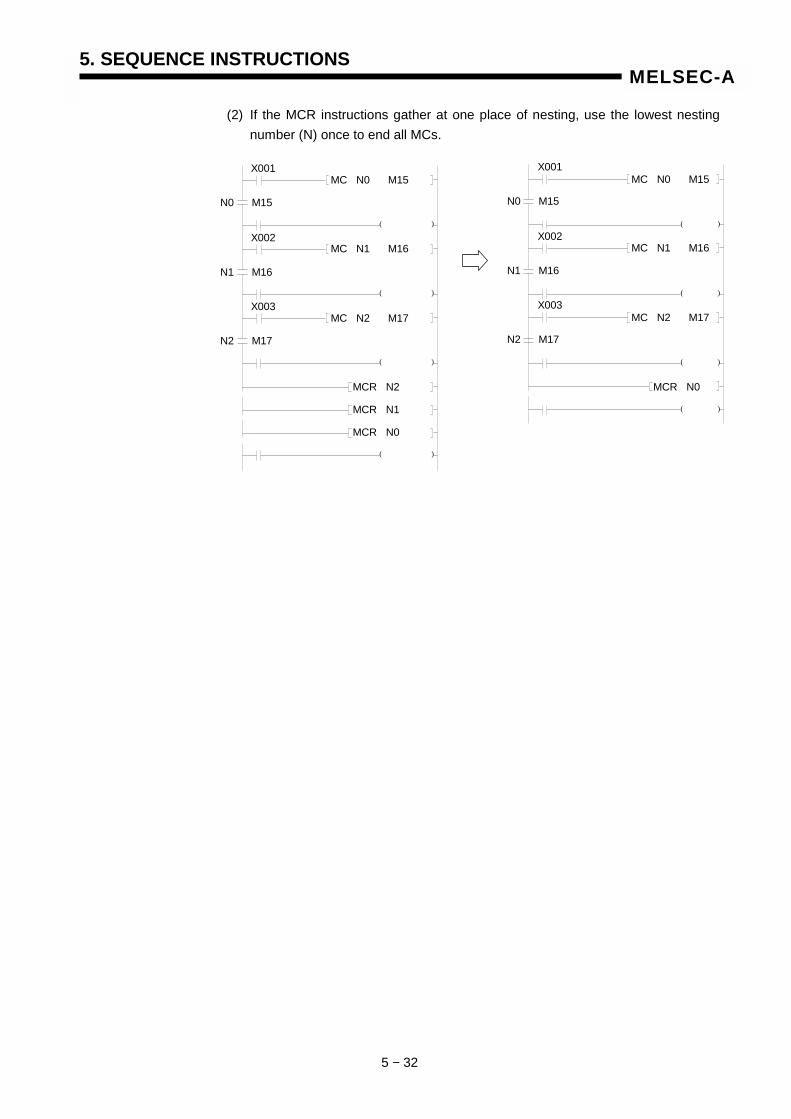
5. SEQUENCE INSTRUCTIONS
5 − 32
MELSEC-A
(2) If the MCR instructions gather at one place of nesting, use the lowest nesting number (N) once to end all MCs.
( )
( )
( )
( )
( )
( )
( )
( )
X001
N0 M15
MC N0 M15
X002
N1 M16
MC N1 M16
X003
N2 M17
MC N2 M17
MCR N2
MCR N1
MCR N0
X001
N0 M15
MC N0 M15
X002
N1 M16
MC N1 M16
X003
N2 M17
MC N2 M17
MCR N0
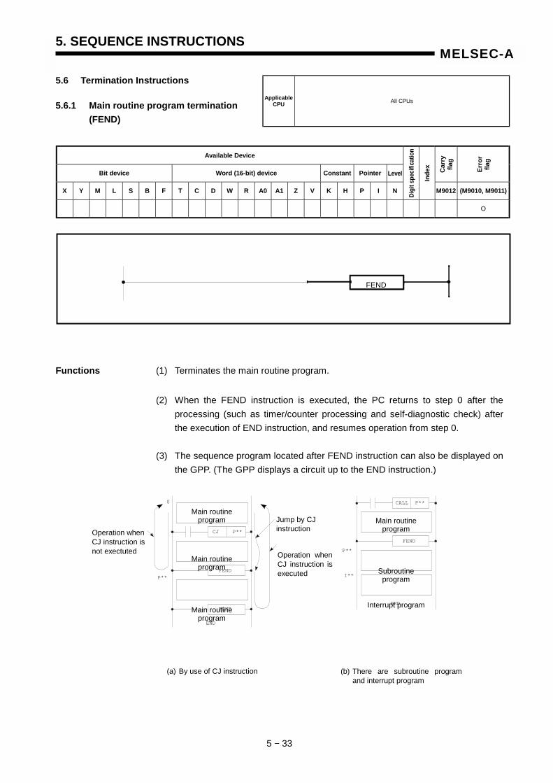
5. SEQUENCE INSTRUCTIONS
5 − 33
MELSEC-A
5.6 Termination Instructions
5.6.1 Main routine program termination (FEND)
Available Device
Bit device Word (16-bit) device Constant Pointer Level Car
ry
flag
Erro
r fla
g
X Y M L S B F T C D W R A0 A1 Z V K H P I N Digi
t spe
cific
atio
n
Inde
x
M9012 (M9010, M9011)
O
Functions (1) Terminates the main routine program. (2) When the FEND instruction is executed, the PC returns to step 0 after the
processing (such as timer/counter processing and self-diagnostic check) after the execution of END instruction, and resumes operation from step 0.
(3) The sequence program located after FEND instruction can also be displayed on
the GPP. (The GPP displays a circuit up to the END instruction.)
Applicable CPU All CPUs
FEND
CJ
FEND
FEND
END
0 CALL
FEND
END
P**
P**
P**
P**
I**
Operation when CJ instruction is not exectuted
Main routine program
Main routine program
Main routine program
Jump by CJ instruction
Operation whenCJ instruction isexecuted
(a) By use of CJ instruction
Main routine program
Subroutine program
Interrupt program
(b) There are subroutine programand interrupt program
5. SEQUENCE INSTRUCTIONS
5 − 34
MELSEC-A
Operation Errors In the following cases, operation error occurs and the PC stops its operation.
• After the CALL(P) instruction is executed, the FEND instruction has been executed before executing the RET instruction.
• After the FOR instruction is executed, the FEND instruction has been executed before executing the NEXT instruction.
5. SEQUENCE INSTRUCTIONS
5 − 35
MELSEC-A
Program Example FEND (1) Program which uses the CJ instruction.
( )
( )
( )
( )
X000 0 Y020
X00B 2 CJ P23
X013 6
When XB is on, jump is made to label P23 and execution is performed from the next step to P23.
Y030
X014 8 Y031
Executed when XB is off.
10 FEND
X001 P23 11
Indicates the end of sequence program when XB is off.
Y022
• Coding 0 LD X000 1 OUT Y020 2 LD X00B 3 CJ P23 6 LD X013 7 OUT Y030 8 LD X014 9 OUT Y031 10 FEND 11 P23 12 LD X001 13 OUT Y022 14 END
5. SEQUENCE INSTRUCTIONS
5 − 36
MELSEC-A
5.6.2 Sequence program termination (END)
Available Device
Bit device Word (16-bit) device Constant Pointer Level Car
ry
flag
Erro
r fla
g
X Y M L S B F T C D W R A0 A1 Z V K H P I N Digi
t spe
cific
atio
n
Inde
x
M9012 (M9010, M9011)
Functions (1) This instruction indicates the end of program. At this step, the scan returns to step 0.
(2) The END instruction cannot be used midway through the sequence program or subsequence program. If END processing is necessary halfway through the program, use the FEND instruction.
(3) When a program is written in the ladder mode of GPP, it is not necessary to input
the END instruction. It is input automatically by performing conversion.
0
Applicable CPU All CPUs
END
When the ladder is displayed,END is omitted.
Sequence program
END
5. SEQUENCE INSTRUCTIONS
5 − 37
MELSEC-A
(4) Use the END and FEND instructions in the main routine program, subroutine program, interrupt program, and subsequence program as shown below.
Fig. 5.1 Use of the END (FEND) Instructions
(5) If the END instruction is not given in the program, operation error occurs and the PC does not run. If parameters are used to set subprogram capacity, operation error occurs when the END instruction is not given in the subprogram.
Operation Errors In the following cases, operation error occurs and the PC stops its operation.
(1) Jump has been made to a step below the END instruction by the CJ, SCJ, or JMP
instruction. (2) The subroutine program or interrupt program located below the END instruction
has been executed.
Main routine program
Subroutine program
(FEND instruction is always required.)
Main sequence program area
Interrupt program
(END instruction is always required.)
Main routine program
(FEND instruction is always required.)
Subroutine program Subsequence program area
Interrupt program
(END instruction is always required.
FEND
END
FEND
END
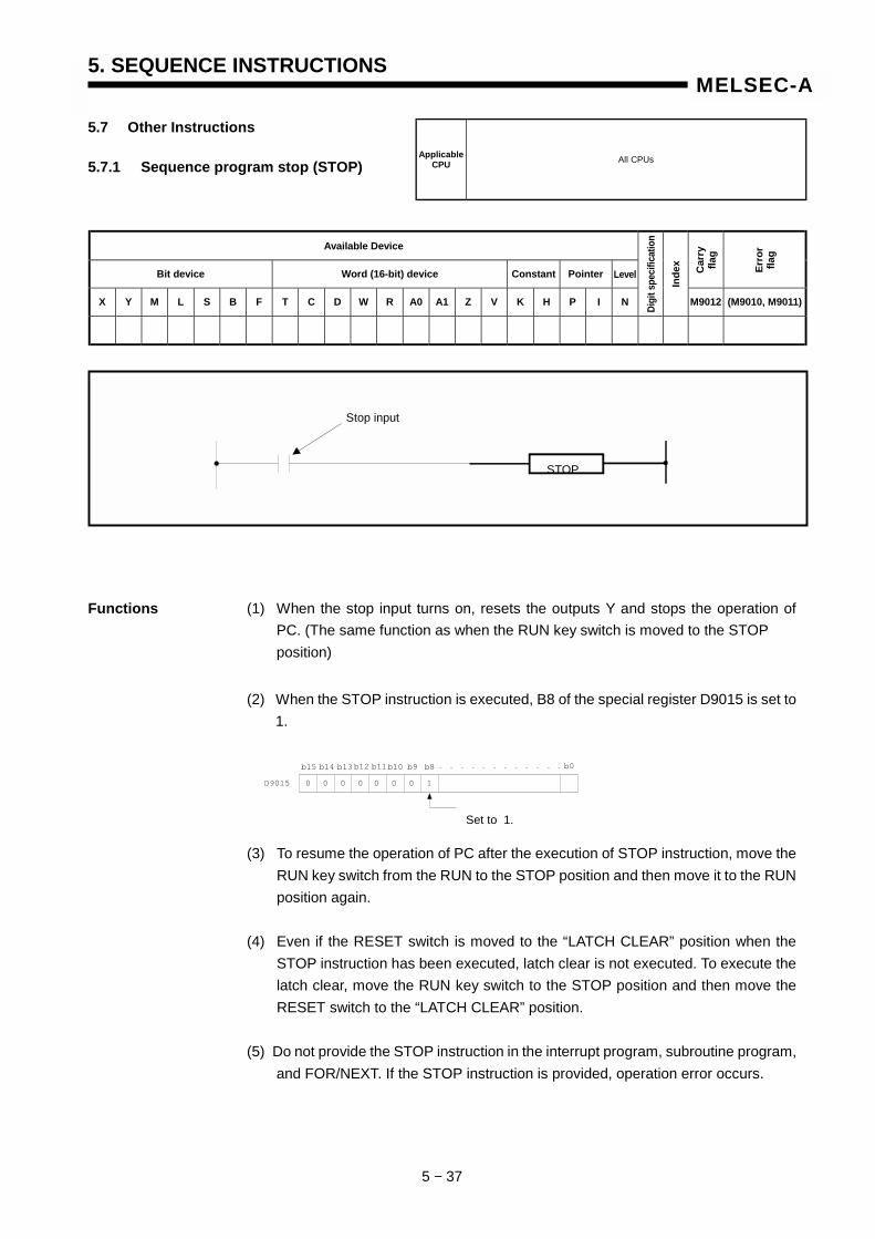
5. SEQUENCE INSTRUCTIONS
5 − 37
MELSEC-A
5.7 Other Instructions
5.7.1 Sequence program stop (STOP)
Available Device
Bit device Word (16-bit) device Constant Pointer Level Car
ry
flag
Erro
r fla
g
X Y M L S B F T C D W R A0 A1 Z V K H P I N Digi
t spe
cific
atio
n
Inde
x
M9012 (M9010, M9011)
Functions (1) When the stop input turns on, resets the outputs Y and stops the operation of PC. (The same function as when the RUN key switch is moved to the STOP position)
(2) When the STOP instruction is executed, B8 of the special register D9015 is set to
1.
(3) To resume the operation of PC after the execution of STOP instruction, move the RUN key switch from the RUN to the STOP position and then move it to the RUN position again.
(4) Even if the RESET switch is moved to the “LATCH CLEAR” position when the
STOP instruction has been executed, latch clear is not executed. To execute the latch clear, move the RUN key switch to the STOP position and then move the RESET switch to the “LATCH CLEAR” position.
(5) Do not provide the STOP instruction in the interrupt program, subroutine program,
and FOR/NEXT. If the STOP instruction is provided, operation error occurs.
Applicable CPU All CPUs
STOP
Stop input
Set to 1.
D9015
b0
0 0 0 0 0 0 0 1
b15 b14 b13b12 b11b10 b9 b8
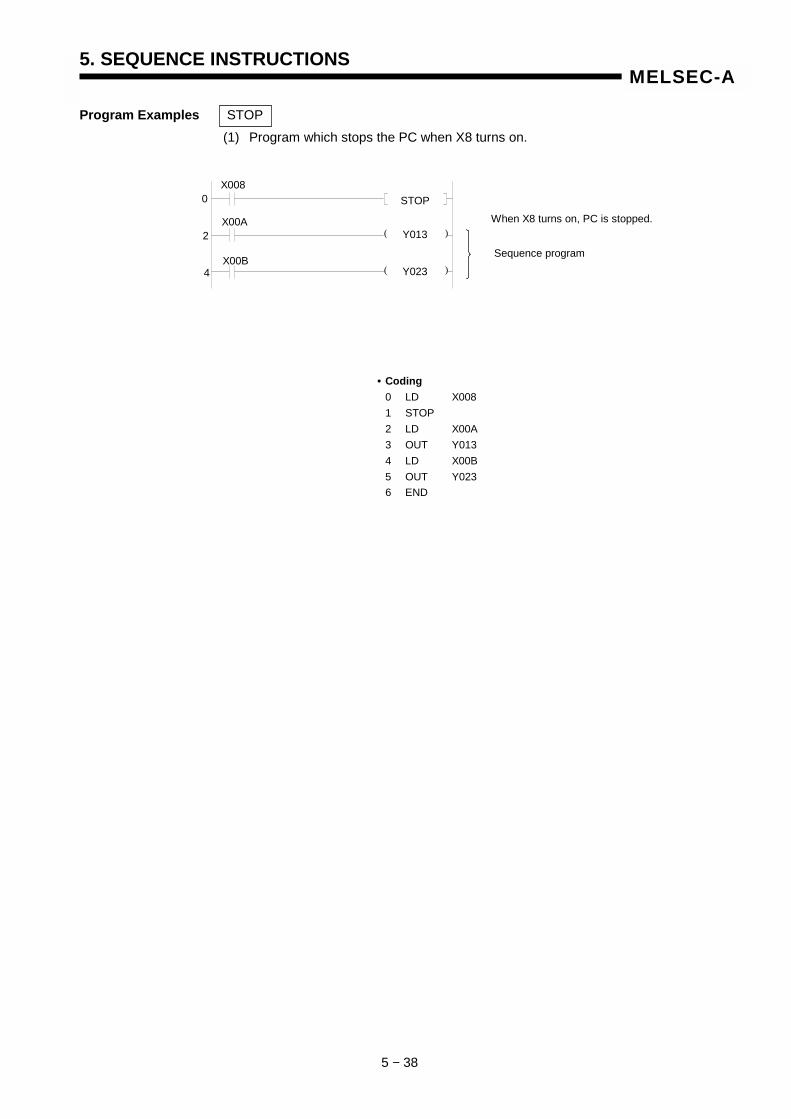
5. SEQUENCE INSTRUCTIONS
5 − 38
MELSEC-A
Program Examples STOP (1) Program which stops the PC when X8 turns on.
( )
( )
X008
X00A
X00B
STOP
Y013
Y023
0
2
4
When X8 turns on, PC is stopped.
Sequence program
• Coding 0 LD X008 1 STOP 2 LD X00A 3 OUT Y013 4 LD X00B 5 OUT Y023 6 END
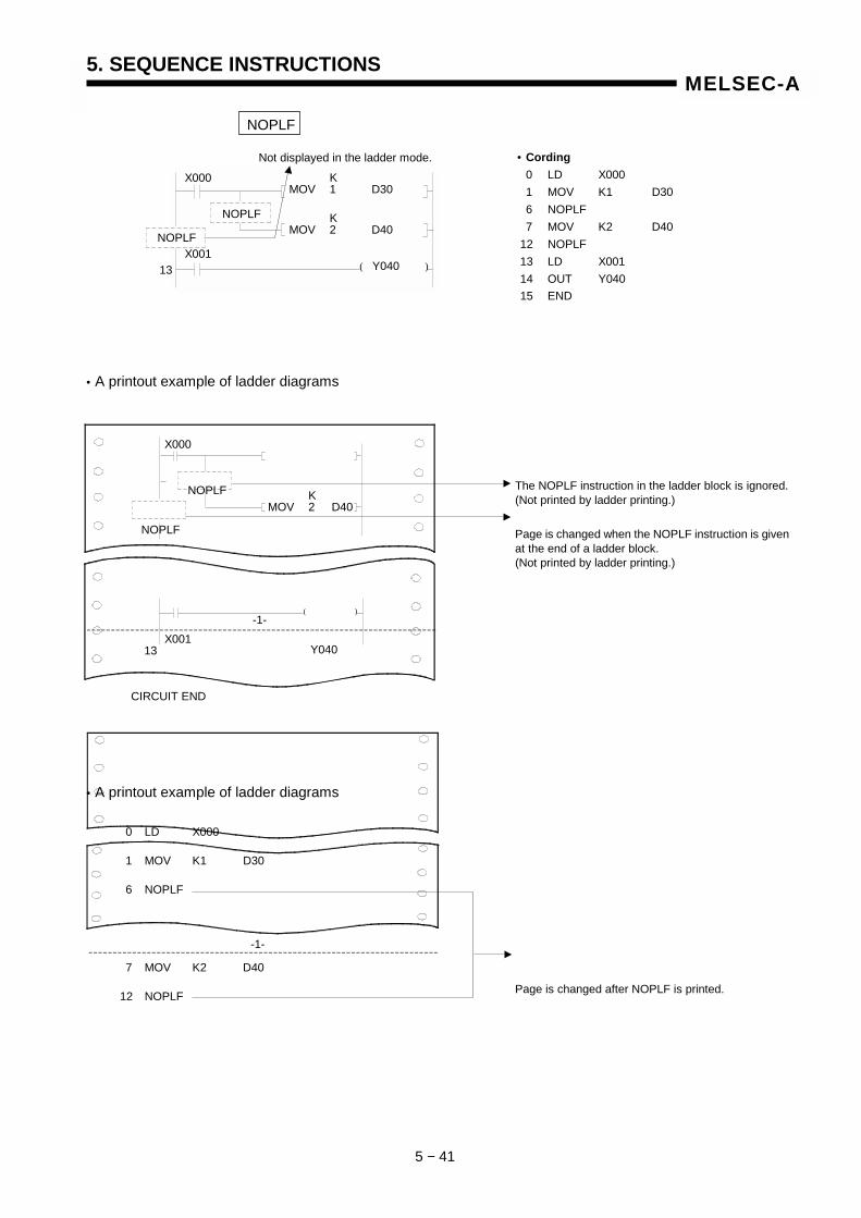
5. SEQUENCE INSTRUCTIONS
5 − 41
MELSEC-A
NOPLF
( )
• Cording 0 LD X000 1 MOV K1 D30 6 NOPLF 7 MOV K2 D40 12 NOPLF 13 LD X001 14 OUT Y040 15 END
• A printout example of ladder diagrams
The NOPLF instruction in the ladder block is ignored. (Not printed by ladder printing.)
Page is changed when the NOPLF instruction is givenat the end of a ladder block. (Not printed by ladder printing.)
( )
X000
X001 13
Not displayed in the ladder mode.
K MOV 1 D30
K MOV 2 D40
Y040
NOPLF
NOPLF
X000
NOPLF K MOV 2 D40
NOPLF
13 Y040
-1- X001
CIRCUIT END
• A printout example of ladder diagrams
Page is changed after NOPLF is printed.
0 LD X000 1 MOV K1 D30 6 NOPLF
-1-
7 MOV K2 D40 12 NOPLF

5. SEQUENCE INSTRUCTIONS
5 − 42
MELSEC-A
-2- 13 LD X001 14 OUT Y040 15 END
6. BASIC INSTRUCTIONS
6 − 1
MELSEC-A
6. BASIC INSTRUCTIONS
The basic instructions are instructions which are capable of handing numeric data expressed in 16 bits and 32 bits, and are classified into the following instructions.
Classification of Basic Instructions Description Ref. Page
Comparison operation instruction Comparison such as =, >, and < 6-2
Arithmetic operation instruction Addition subtraction, multiplication,
and division in BIN and BCD. INC, DEC
6-8
BCD ↔ BIN conversion instruction Conversion from BCD to BIN and from BIN to BCD 6-38
Data transfer instruction Transfer of specified data 6-46
Program branch instruction Jump, call, interrupt enable/disable 6-58
Program switching instruction Switching between main and subprogram 6-69
Refresh instruction Data link refresh and I/O partial refresh 6-82
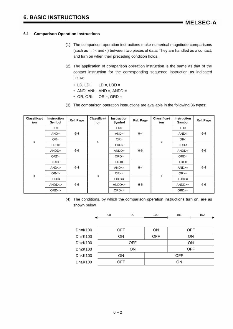
6. BASIC INSTRUCTIONS
6 − 2
MELSEC-A
6.1 Comparison Operation Instructions
(1) The comparison operation instructions make numerical magnitude comparisons (such as =, >, and <) between two pieces of data. They are handled as a contact, and turn on when their preceding condition holds.
(2) The application of comparison operation instruction is the same as that of the contact instruction for the corresponding sequence instruction as indicated below:
• LD, LDI: LD =, LDD = • AND, ANI: AND =, ANDD = • OR, ORI: OR =, ORD =
(3) The comparison operation instructions are available in the following 36 types:
Classifica-tion
Instruction Symbol Ref. Page Classifica-t
ion Instruction
Symbol Ref. Page Classifica-tion
Instruction Symbol Ref. Page
LD= LD> LD<
AND= AND> AND<
OR=
6-4
OR>
6-4
OR<
6-4
LDD= LDD> LDD<
ANDD= ANDD> ANDD<
=
ORD=
6-6
>
ORD>
6-6
<
ORD<
6-6
LD<> LD<= LD>=
AND<> AND<= AND>=
OR<>
6-4
OR<=
6-4
OR>=
6-4
LDD<> LDD<= LDD>=
ANDD<> ANDD<= ANDD>=
≠
ORD<>
6-6
≤
ORD<=
6-6
≥
ORD>=
6-6
(4) The conditions, by which the comparison operation instructions turn on, are as shown below.
Dn=K100 OFF ON OFF
Dn≠K100 ON OFF ON
Dn>K100 OFF ON
Dn≤K100 ON OFF
Dn<K100 ON OFF
Dn≥K100 OFF ON
98 99 100 101 102
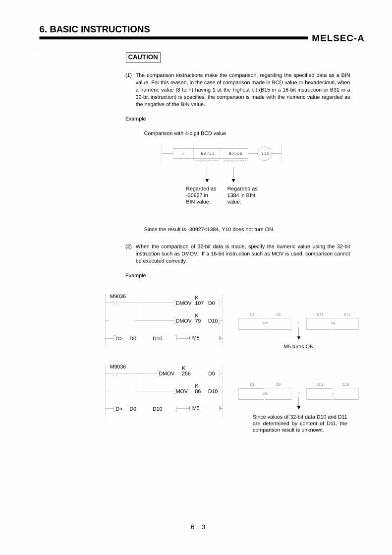
6. BASIC INSTRUCTIONS
6 − 3
MELSEC-A
CAUTION
(1) The comparison instructions make the comparison, regarding the specified data as a BIN value. For this reason, in the case of comparison made in BCD value or hexadecimal, when a numeric value (8 to F) having 1 at the highest bit (B15 in a 16-bit instruction or B31 in a 32-bit instruction) is specifies, the comparison is made with the numeric value regarded as the negative of the BIN value. Example Comparison with 4-digit BCD value
Since the result is -30927<1384, Y10 does not turn ON.
(2) When the comparison of 32-bit data is made, specify the numeric value using the 32-bit instruction such as DMOV. If a 16-bit instruction such as MOV is used, comparison cannot be executed correctly. Example
H8731 H0568 Y10>
Regarded as -30927 in BIN value.
Regarded as 1384 in BIN value.
( )
( )
107
D1 D0
79
D11 D10
>
256
D1 D0
?
D11 D10
?
M9036 K DMOV 107 D0
D> D0 D10 M5
K DMOV 79 D10
M9036 K DMOV 256 D0
D> D0 D10 M5
K MOV 86 D10
M5 turns ON.
Since values of 32-bit data D10 and D11 are determined by content of D11, the comparison result is unknown.

6. BASIC INSTRUCTIONS
6 − 4
MELSEC-A
6.1.1 16-bit data comparison (=, <>, >, <=, <, >=)
Available Device
Bit device Word (16-bit) device Constant Pointer Level Car
ry
flag
Erro
r fla
g
X Y M L S B F T C D W R A0 A1 Z V K H P I N Digi
t spe
cific
atio
n
Inde
x
M9012 (M9010, M9011)
(S1) O O O O O O O O O O O O O O O O O O
(S2) O O O O O O O O O O O O O O O O O O
K1 to K4
O O
Functions (1) Handled as a NO contact and used for the comparison of 16bits. (2) The comparison operation result is as shown below:
Instruction Symbol in Condition
Comparison Operation
Result
Instruction Symbol in Condition
Comparison Operation
Result
= (S1) = (S2) = (S1) ≠ (S2)
<> (S1) ≠ (S2) <> (S1) = (S2)
> (S1) > (S2) > (S1) ≤ (S2)
<= (S1) ≤ (S2) <= (S1) > (S2)
< (S1) < (S2) < (S1) ≥ (S2)
>= (S1) ≥ (S2)
Continuity status
>= (S1) < (S2)
Non-Continuity status
Execution The execution conditions of LD , AND , and OR are as indicated below. Conditions
Instruction Execution Condition
LD Executed per scan.
AND Executed only when the preceding contact instruction is on.
OR Executed per scan.
Applicable CPU All CPUs
(S1)
(S2)
Compared data or head number of device which stores compared data
Setting data
=, <>,> <=, <, >=
Indicates the instruction symbol. LD
AND
OR
(S1) (S2)
(S1) (S2)
(S1) (S2)
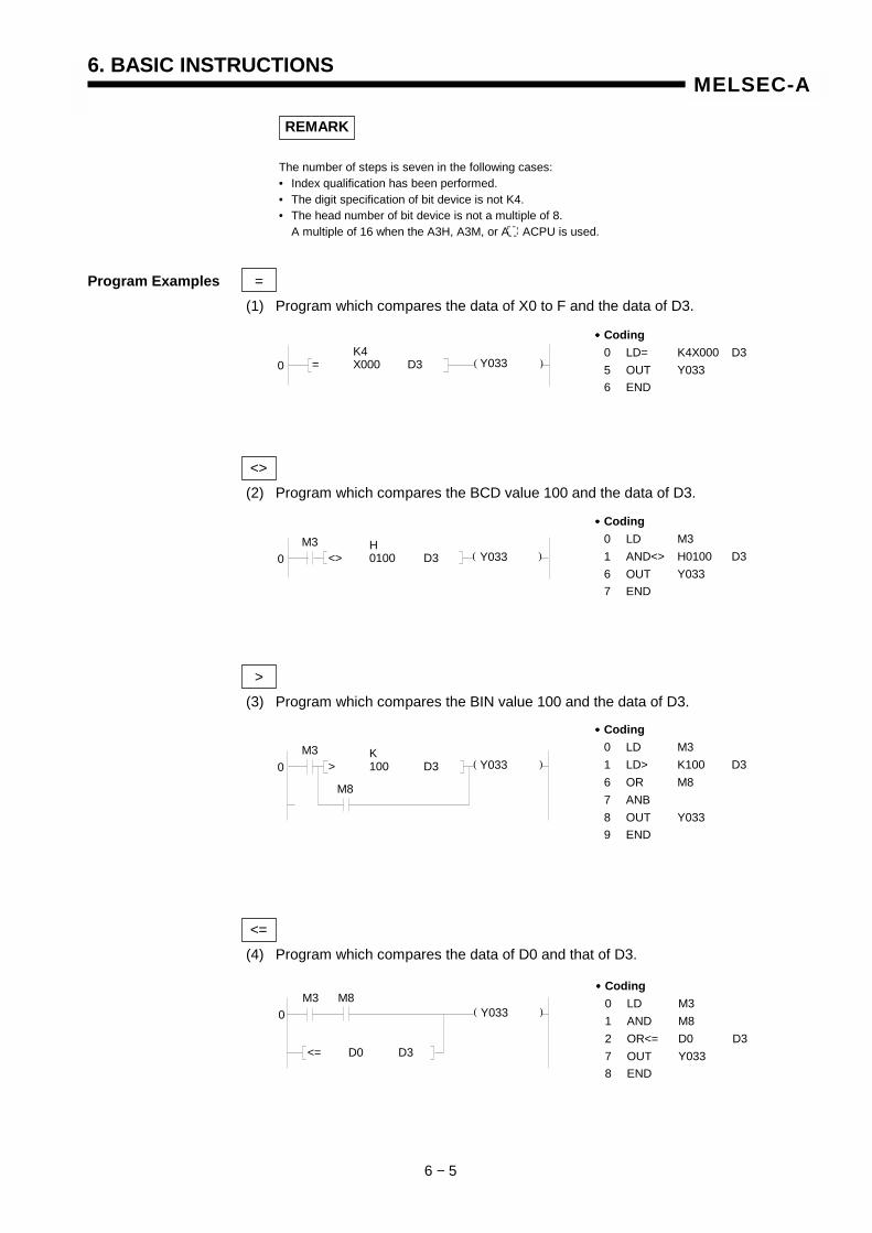
6. BASIC INSTRUCTIONS
6 − 5
MELSEC-A
REMARK
The number of steps is seven in the following cases: • Index qualification has been performed. • The digit specification of bit device is not K4. • The head number of bit device is not a multiple of 8. A multiple of 16 when the A3H, A3M, or A ACPU is used.
Program Examples = (1) Program which compares the data of X0 to F and the data of D3.
<> (2) Program which compares the BCD value 100 and the data of D3.
> (3) Program which compares the BIN value 100 and the data of D3.
<= (4) Program which compares the data of D0 and that of D3.
( )0 K4 = X000 D3 Y033
•••• Coding 0 LD= K4X000 D3 5 OUT Y033 6 END
( )0 H <> 0100 D3 Y033
•••• Coding 0 LD M3 1 AND<> H0100 D3 6 OUT Y033 7 END
M3
( )0 K > 100 D3 Y033
•••• Coding 0 LD M3 1 LD> K100 D3 6 OR M8 7 ANB 8 OUT Y033 9 END
M3
M8
( )0
<= D0 D3
Y033
•••• Coding 0 LD M3 1 AND M8 2 OR<= D0 D3 7 OUT Y033 8 END
M3 M8
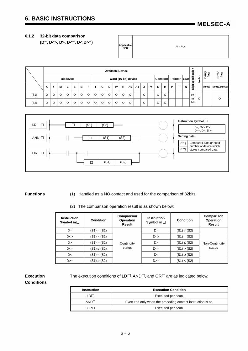
6. BASIC INSTRUCTIONS
6 − 6
MELSEC-A
6.1.2 32-bit data comparison (D=, D<>, D>, D<=, D<,D>=)
Available Device
Bit device Word (16-bit) device Constant Pointer Level Car
ry
flag
Erro
r fla
g
X Y M L S B F T C D W R A0 A1 Z V K H P I N Digi
t spe
cific
atio
n
Inde
x
M9012 (M9010, M9011)
(S1) O O O O O O O O O O O O O O O O
(S2) O O O O O O O O O O O O O O O O
K1 to K8
O O
Functions (1) Handled as a NO contact and used for the comparison of 32bits. (2) The comparison operation result is as shown below:
Instruction Symbol in Condition
Comparison Operation
Result
Instruction Symbol in Condition
Comparison Operation
Result
D= (S1) = (S2) D= (S1) ≠ (S2)
D<> (S1) ≠ (S2) D<> (S1) = (S2)
D> (S1) > (S2) D> (S1) ≤ (S2)
D<= (S1) ≤ (S2) D<= (S1) > (S2)
D< (S1) < (S2) D< (S1) ≥ (S2)
D>= (S1) ≥ (S2)
Continuity status
D>= (S1) < (S2)
Non-Continuity status
Execution The execution conditions of LD , AND , and OR are as indicated below. Conditions
Instruction Execution Condition
LD Executed per scan.
AND Executed only when the preceding contact instruction is on.
OR Executed per scan.
Applicable CPU All CPUs
(S1)
(S2)
Compared data or head number of device which stores compared data
Setting data
D=, D<>,D> D<=, D<, D>=
Instruction symbol . LD
AND
OR
(S1) (S2)
(S1) (S2)
(S1) (S2)
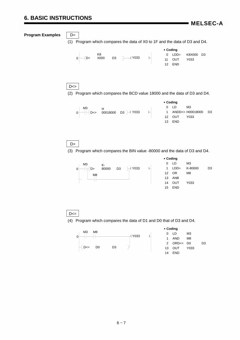
6. BASIC INSTRUCTIONS
6 − 7
MELSEC-A
Program Examples D= (1) Program which compares the data of X0 to 1F and the data of D3 and D4.
D<>
(2) Program which compares the BCD value 18000 and the data of D3 and D4.
D> (3) Program which compares the BIN value -80000 and the data of D3 and D4.
D<=
(4) Program which compares the data of D1 and D0 that of D3 and D4.
( )0 K8 D= X000 D3 Y033
•••• Coding 0 LDD= K8X000 D3 11 OUT Y033 12 END
( )0 H D<> 00018000 D3 Y033
•••• Coding 0 LD M3 1 ANDD<> H00018000 D3 12 OUT Y033 13 END
M3
( )0 K- D> 80000 D3 Y033
•••• Coding 0 LD M3 1 LDD> K-80000 D3 12 OR M8 13 ANB 14 OUT Y033 15 END
M3
M8
( )0
D<= D0 D3
Y033
•••• Coding 0 LD M3 1 AND M8 2 ORD<= D0 D3 13 OUT Y033 14 END
M3 M8
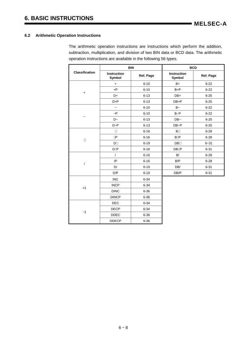
6. BASIC INSTRUCTIONS
6 − 8
MELSEC-A
6.2 Arithmetic Operation Instructions
The arithmetic operation instructions are instructions which perform the addition, subtraction, multiplication, and division of two BIN data or BCD data. The arithmetic operation instructions are available in the following 56 types.
BIN BCD Classification Instruction
Symbol Ref. Page Instruction Symbol Ref. Page
+ 6-10 B+ 6-22
+P 6-10 B+P 6-22
D+ 6-13 DB+ 6-25 +
D+P 6-13 DB+P 6-25
− 6-10 B− 6-22
−P 6-10 B−P 6-22
D− 6-13 DB− 6-25 −
D−P 6-13 DB−P 6-25
∗ 6-16 B∗ 6-28
∗ P 6-16 B∗ P 6-28
D∗ 6-19 DB∗ 6−31 ∗
D∗ P 6-19 DB∗ P 6-31
/ 6-16 B/ 6-28
/P 6-16 B/P 6-28
D/ 6-19 DB/ 6-31 /
D/P 6-19 DB/P 6-31
INC 6-34
INCP 6-34
DINC 6-36 +1
DINCP 6-36
DEC 6-34
DECP 6-34
DDEC 6-36 −1
DDECP 6-36
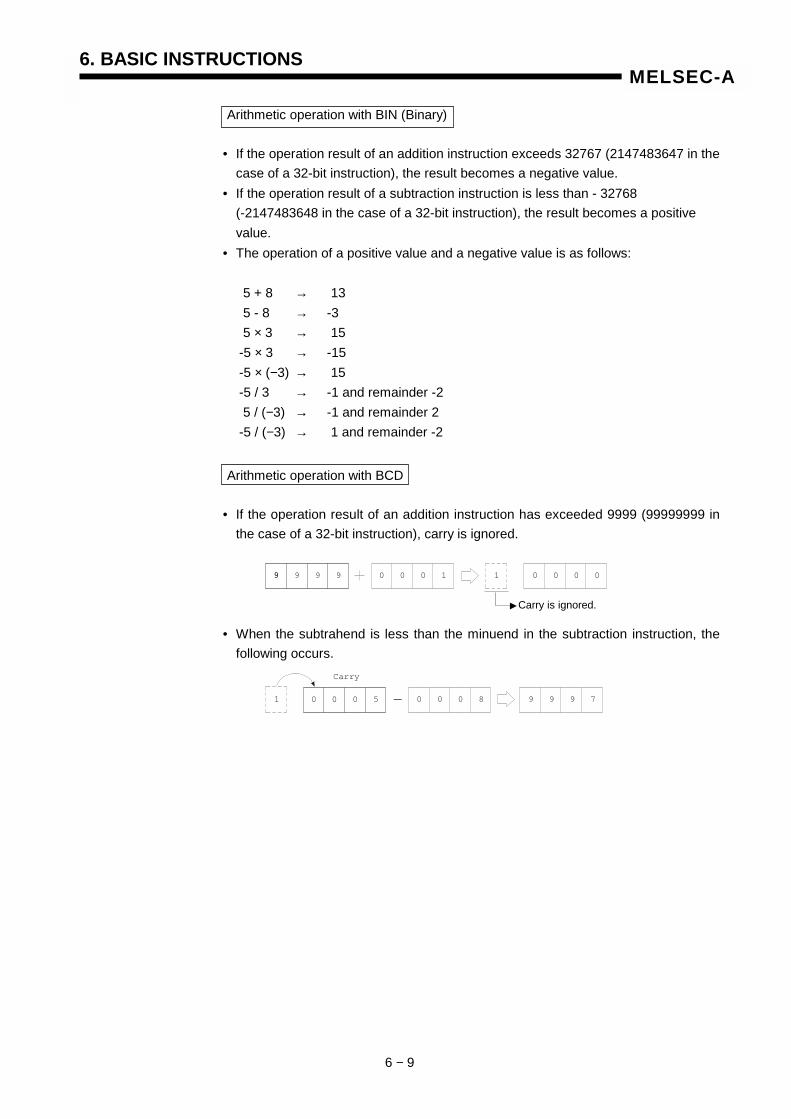
6. BASIC INSTRUCTIONS
6 − 9
MELSEC-A
Arithmetic operation with BIN (Binary)
• If the operation result of an addition instruction exceeds 32767 (2147483647 in the case of a 32-bit instruction), the result becomes a negative value.
• If the operation result of a subtraction instruction is less than - 32768 (-2147483648 in the case of a 32-bit instruction), the result becomes a positive value.
• The operation of a positive value and a negative value is as follows: 5 + 8 → 13 5 - 8 → -3 5 × 3 → 15 -5 × 3 → -15 -5 × (−3) → 15 -5 / 3 → -1 and remainder -2 5 / (−3) → -1 and remainder 2 -5 / (−3) → 1 and remainder -2
Arithmetic operation with BCD
• If the operation result of an addition instruction has exceeded 9999 (99999999 in the case of a 32-bit instruction), carry is ignored.
• When the subtrahend is less than the minuend in the subtraction instruction, the following occurs.
Carry is ignored.
99 9 9 9 0 0 0 1 1 0 0 0 0
0 0 0 5 0 0 0 81 9 9 9 7
Carry
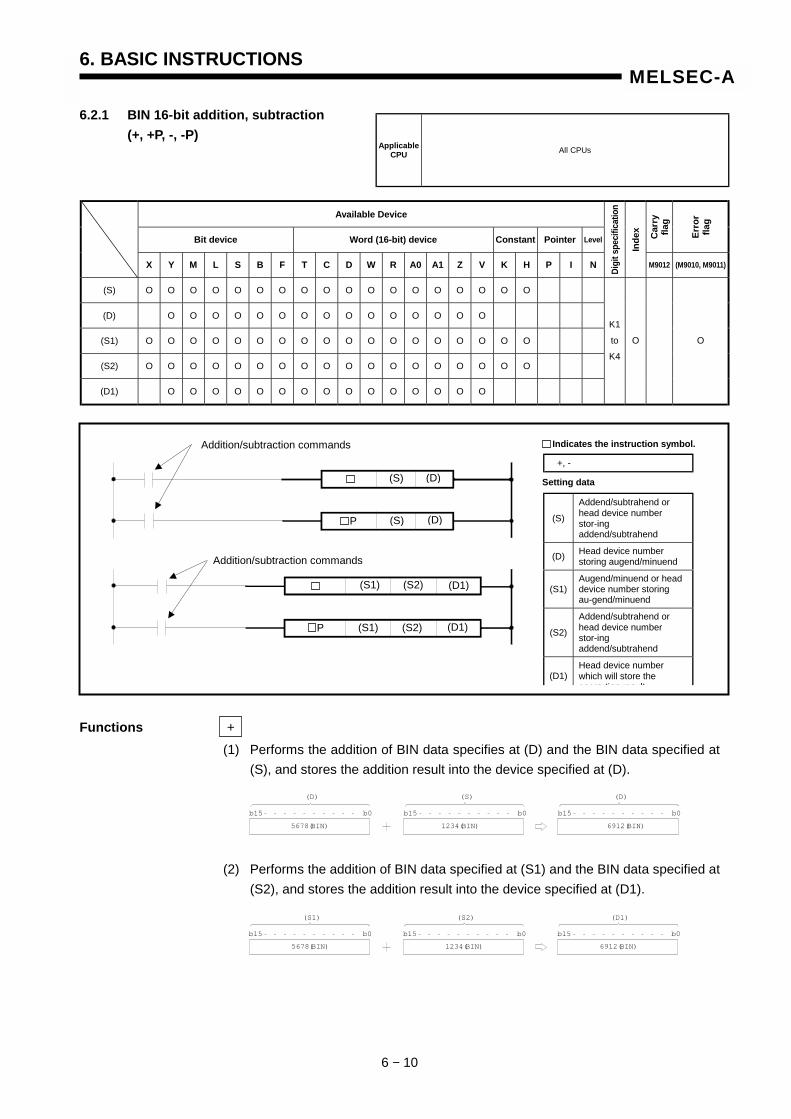
6. BASIC INSTRUCTIONS
6 − 10
MELSEC-A
6.2.1 BIN 16-bit addition, subtraction (+, +P, -, -P)
Available Device
Bit device Word (16-bit) device Constant Pointer Level Car
ry
flag
Erro
r fla
g
X Y M L S B F T C D W R A0 A1 Z V K H P I N Digi
t spe
cific
atio
n
Inde
x
M9012 (M9010, M9011)
(S) O O O O O O O O O O O O O O O O O O
(D) O O O O O O O O O O O O O O O
(S1) O O O O O O O O O O O O O O O O O O
(S2) O O O O O O O O O O O O O O O O O O
(D1) O O O O O O O O O O O O O O O
K1
to
K4
O O
Functions + (1) Performs the addition of BIN data specifies at (D) and the BIN data specified at
(S), and stores the addition result into the device specified at (D).
(2) Performs the addition of BIN data specified at (S1) and the BIN data specified at (S2), and stores the addition result into the device specified at (D1).
Applicable CPU All CPUs
(S)
Addend/subtrahend or head device number stor-ing addend/subtrahend
(D) Head device number storing augend/minuend
(S1) Augend/minuend or head device number storing au-gend/minuend
(S2)
Addend/subtrahend or head device number stor-ing addend/subtrahend
(D1) Head device number which will store the opera tion result
Setting data
+, -
Indicates the instruction symbol.
b15 b0
(D)
5678(BIN) 1234(BIN)
b15 b0 b15 b0
6912(BIN)
(S) (D)
b15 b0
(S1)
5678(BIN) 1234(BIN)
b15 b0 b15 b0
6912(BIN)
(S2) (D1)
Addition/subtraction commands
Addition/subtraction commands
(S) (D)
(S) (D)
(S1) (S2) (D1)
(S1) (S2) (D1)
P
P
6. BASIC INSTRUCTIONS
6 − 11
MELSEC-A
(3) At (S), (S1), (S2) and (D), -32768 to 32767 (BIN 16 bits) can be specified. (4) The judgment of whether the data of (S), (S1), (S2) and (D) are positive or
negative is made at the highest bit (b15). 0 ⋅⋅⋅⋅⋅⋅ Positive 1 ⋅⋅⋅⋅⋅⋅ Negative (5) When the 0th bit has underflown, the carry flag does not turn on. When the 15th bit has overflown, the carry flag does not turn on.
Functions - (1) Performs the subtraction of BIN data specified at (D) and the BIN data specified
at (S), and stores the subtraction result into the device specified at (D).
(2) Performs the subtraction of BIN data specified at (S1) and the BIN data specified at (S2), and stores the subtraction result into the device specified at (D1).
(3) At (S), (S1), (S2) and (D), -32768 to 32767 (BIN 16 bits) can be specified. (4) The judgement of whether the dates of (S), (S1), (S2) and (D) are positive or
negative is made at the highest bit (b15). 0 …….. Positive 1 …….. Negative (5) When the 0th bit has underflown, the carry flag does not turn on. When the 15th bit has overflown, the carry flag does not turn on.
b15 b0
(D)
5678(BIN) 1234(BIN)
b15 b0 b15 b0
4444(BIN)
(S) (D)
b15 b0
(S1)
5678(BIN) 1234(BIN)
b15 b0 b15 b0
4444(BIN)
(S2) (D1)
6. BASIC INSTRUCTIONS
6 − 12
MELSEC-A
Execution Conditions
Program Examples + Program which adds the content of A0 to the content of D3 and outputs the result to Y38 to 3F when X5 turns on.
- Program which outputs the difference between the set value and present value timer T3 to Y40 to 53 in BCD.
• Coding 0 LD X005 1 +P D3 A0 K2Y038 8 END
0X005 P K2
+ D3 A0 Y038
• Coding 0 LD X003 1 OUT T3 K18000 2 LD M9036 3 -P K18000 T3 D3 10 DBCD D3 K5Y040 19 END
( )0
2
X003
M9036
K18000 T3
P K - 18000 T3 D3
K5 DBCD D3 Y040
OFF
ON
Addition/subtraction command
Executed per scan
Executed per scan
Executed only once
Executed only once
P
OFF ON
6. BASIC INSTRUCTIONS
6 − 13
MELSEC-A
6.2.2 BIN 32-bit addition, subtraction (D+, D+P, D-, D-P)
Available Device
Bit device Word (16-bit) device Constant Pointer Level Car
ry
flag
Erro
r fla
g
X Y M L S B F T C D W R A0 A1 Z V K H P I N Digi
t spe
cific
atio
n
Inde
x
M9012 (M9010, M9011)
(S) O O O O O O O O O O O O O O O O
(D) O O O O O O O O O O O O O
(S1) O O O O O O O O O O O O O O O O
(S2) O O O O O O O O O O O O O O O O
(D1) O O O O O O O O O O O O O
K1
to
K8
O O
Functions D+ (1) Performs the addition of BIN data specified at (D) and the BIN data specified at
(S), and stores the addition result into the device specified at (D).
(2) Performs the addition of BIN data specified at (S1) and the BIN data specified at (S2), and stores the addition result into the device specified at (D1).
Applicable CPU All CPUs
(S)
Addend/subtrahend or head device number stor-ing addend/subtrahend
(D) Head device number storing augend/minuend
(S1) Augend/minuend or head device number storing au-gend/minuend
(S2)
Addend/subtrahend or head device number stor-ing addend/subtrahend
(D1) Head device number which will store the opera tion result
Setting data
D+, D-
Indicates the instruction symbol.
Addition/subtraction commands
Addition/subtraction commands
(S) (D)
(D)
(S1)
(S)
(S2) (D1)
(S1) (S2) (D1)
P
P
b31 b16
(D)+1
567890(BIN) 123456(BIN)
b0
691346(BIN)
(D)
b15 b31 b16
(S)+1
b0
(S)
b15 b31 b16
(D)+1
b0
(D)
b15
b31 b16
(S1)+1
567890(BIN) 123456(BIN)
b0
691346(BIN)
(S1)
b15 b31 b16
(S2)+1
b0
(S2)
b15 b31 b16
(D1)+1
b0
(D1)
b15
6. BASIC INSTRUCTIONS
6 − 14
MELSEC-A
(3) At (S), (S1), (S2) and (D), -2147483648 to 2147483647 (BIN 32 bits) can be specified.
(4) The judgement of whether the datas of (S), (S1), (S2) and (D) are positive or
negative is made at the highest bit (b31). 0……. Positive 1……. Negative
(5) When the 0th bit has underflown, the carry flag does not turn on.
When the 31st bit has overflown, the carry flag does not turn on.
D-
(1) Performs the subtraction of BIN data specified at (D) and the BIN data specified at (S), and stores the addition result into the device specified at (D).
(2) Performs the subtraction of device specified at (S1) and the device specified at (S2), and stores the result into the device specified at (D1).
(3) At (S), (S1), (S2) and (D), -2147483648 to 2147483647 (BIN 32 bits) can be specified.
(4) The judgement of whether the dates of (S), (S1), (S2) and (D) are positive or
negative is made at the highest bit (b31). 0……. Positive 1……. Negative
(5) When the 0th bit has underflown, the carry flag does not turn on.
When the 31st bit has overflown, the carry flag does not turn on.
b31 b16
(D)+1
567890(BIN) 123456(BIN)
b0
444434(BIN)
(D)
b15 b31 b16
(S)+1
b0
(S)
b15 b31 b16
(D)+1
b0
(D)
b15
b31 b16
(S1)+1
567890(BIN) 123456(BIN)
b0
444434(BIN)
(S1)
b15 b31 b16
(S2)+1
b0
(S2)
b15 b31 b16
(D1)+1
b0
(D1)
b15
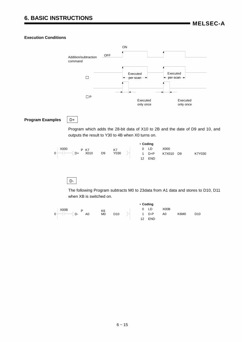
6. BASIC INSTRUCTIONS
6 − 15
MELSEC-A
Execution Conditions
Program Examples D+
Program which adds the 28-bit data of X10 to 2B and the date of D9 and 10, and outputs the result to Y30 to 4B when X0 turns on.
D-
The following Program subtracts M0 to 23data from A1 data and stores to D10, D11 when XB is switched on.
Addition/subtraction command
Executed per scan
Executed per scan
Executed only once
• Coding 0 LD X000 1 D+P K7X010 D9 K7Y030 12 END
0 X000 P K7 K7
D+ X010 D9 Y030
• Coding 0 LD X00B 1 D-P A0 K6M0 D10 12 END
0 X00B P K6
D- A0 M0 D10
P
ON
OFF
Executed only once

6. BASIC INSTRUCTIONS
6 − 16
MELSEC-A
6.2.3 BIN 16-bit multiplication, division (*, *P, /, /P)
Available Device
Bit device Word (16-bit) device Constant Pointer Level Car
ry
flag
Erro
r fla
g
X Y M L S B F T C D W R A0 A1 Z V K H P I N Digi
t spe
cific
atio
n
Inde
x
M9012 (M9010, M9011)
(S1) O O O O O O O O O O O O O O O O O O
(S2) O O O O O O O O O O O O O O O O O O
(D) O O O O O O O O O O O O O
K1
to
K4
O O
Functions * (1) Performs the multiplication of BIN data specified at (S1) and the BIN data
specified at (S2), and stores the multiplication result into the device specified at (D).
(2) When (D) is a bit device, specify the bits, beginning with the lower bits. Example K1: Lower 4 bits (b0 to 3) K4: Lower 16 bits (b0 to 15) K8: 32 bits (b0 to 31) (3) At (S1) and (S2), -32768 to 32767 (BIN 16 bits) can be specified. (4) The judgment of whether the data of (S1) and (S2) are positive or negative is
made at the highest bit (b15) and that of (D), at (b31).
Applicable CPU All CPUs
(S1) Multiplicand/dividend or head device number storing multiplier/dividend
(S2) Multiplicand/divider or head device number storing multiplier/divider
(D) Head device number which will store the result
Setting data
∗ , /
Indicates the instruction symbol. Multiplication/division commands
(D) (S1)
(S1) (S2)
(S2)
(D)
P
b15 b0
(S1)
5678(BIN) 1234(BIN)
b15 b0
7006652(BIN)
(S2)
b31 b16
(D)+1
b0
(D)
b15
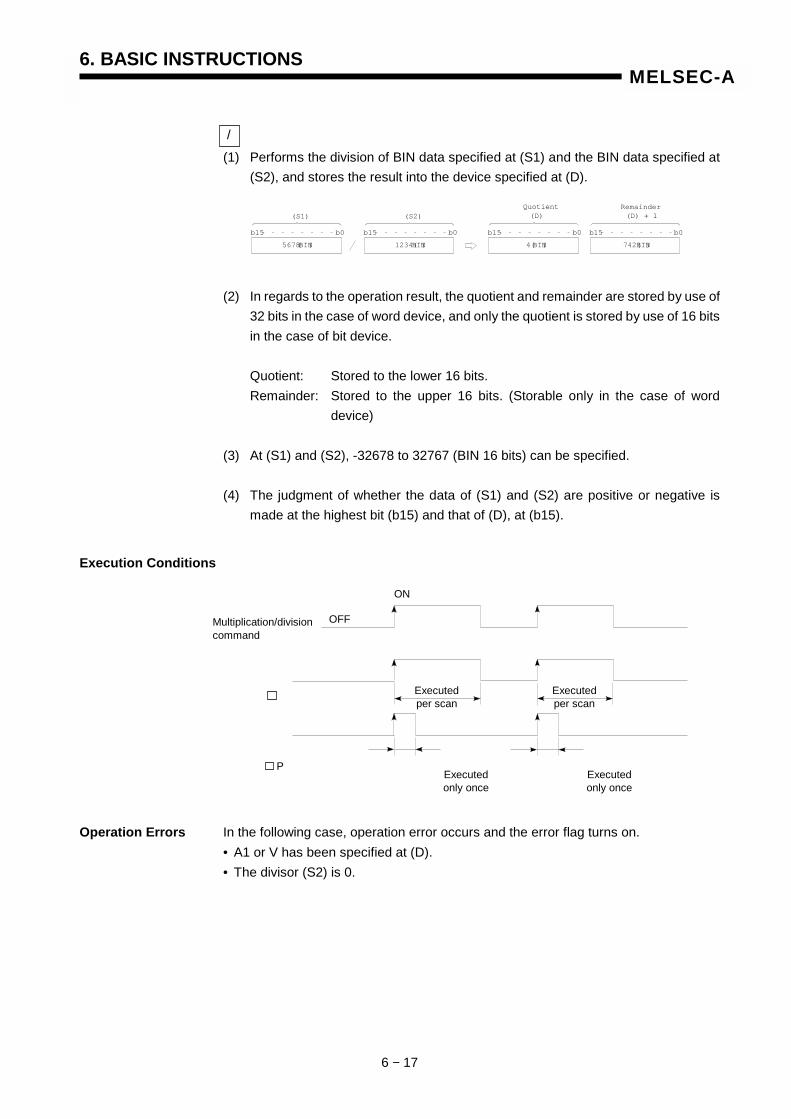
6. BASIC INSTRUCTIONS
6 − 17
MELSEC-A
/ (1) Performs the division of BIN data specified at (S1) and the BIN data specified at
(S2), and stores the result into the device specified at (D).
(2) In regards to the operation result, the quotient and remainder are stored by use of 32 bits in the case of word device, and only the quotient is stored by use of 16 bits in the case of bit device.
Quotient: Stored to the lower 16 bits. Remainder: Stored to the upper 16 bits. (Storable only in the case of word
device) (3) At (S1) and (S2), -32678 to 32767 (BIN 16 bits) can be specified. (4) The judgment of whether the data of (S1) and (S2) are positive or negative is
made at the highest bit (b15) and that of (D), at (b15).
Execution Conditions
Operation Errors In the following case, operation error occurs and the error flag turns on. • A1 or V has been specified at (D). • The divisor (S2) is 0.
b15 b0
(S2)
1234( BIN)
b15 b0
Quotient(D)
b15 b0
742( BIN)
b15 b0
(S1)
5678 (BIN)
Remainder(D) + 1
4( BIN)
Multiplication/divisioncommand
Executed per scan
Executed per scan
Executed only once
P
ON
OFF
Executed only once
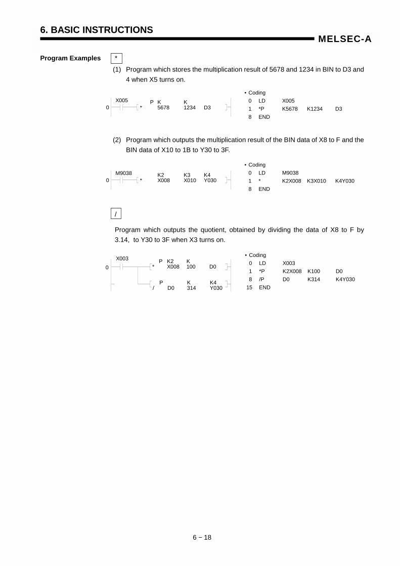
6. BASIC INSTRUCTIONS
6 − 18
MELSEC-A
Program Examples * (1) Program which stores the multiplication result of 5678 and 1234 in BIN to D3 and
4 when X5 turns on.
(2) Program which outputs the multiplication result of the BIN data of X8 to F and the BIN data of X10 to 1B to Y30 to 3F.
/
Program which outputs the quotient, obtained by dividing the data of X8 to F by 3.14, to Y30 to 3F when X3 turns on.
• Coding 0 LD X005 1 *P K5678 K1234 D3 8 END
0 X005 P K K
* 5678 1234 D3
• Coding 0 LD M9038 1 * K2X008 K3X010 K4Y030 8 END
0 M9038 K2 K3 K4
* X008 X010 Y030
• Coding 0 LD X003 1 *P K2X008 K100 D0 8 /P D0 K314 K4Y030 15 END
0 X003 P K2 K
* X008 100 D0
P K K4 / D0 314 Y030
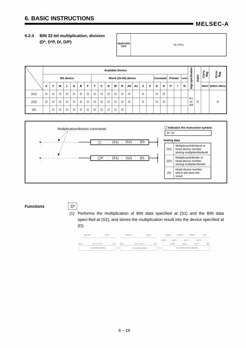
6. BASIC INSTRUCTIONS
6 − 19
MELSEC-A
6.2.4 BIN 32-bit multiplication, division (D*, D*P, D/, D/P)
Available Device
Bit device Word (16-bit) device Constant Pointer Level Car
ry
flag
Erro
r fla
g
X Y M L S B F T C D W R A0 A1 Z V K H P I N Digi
t spe
cific
atio
n
Inde
x
M9012 (M9010, M9011)
(S1) O O O O O O O O O O O O O O O O
(S2) O O O O O O O O O O O O O O O O
(D) O O O O O O O O O O O
K1 to K8
O O
Functions D* (1) Performs the multiplication of BIN data specified at (S1) and the BIN data
speci-fied at (S2), and stores the multiplication result into the device specified at (D).
Applicable CPU All CPUs
b31 b16
(S1)+1 (S1)
b15 b31 b16
(S2)+1 (S2)
b15b0 b0
(D)+3 (D)+2 (D)+1 (D)
b63 b47 b31 b15
b48 b32 b16 b0
567890(BIN) 123456(BIN) 70109427840(BIN)
(S1) Multiplicand/dividend or head device number storing multiplier/dividend
(S2) Multiplicand/divider or head device number storing multiplier/divider
(D) Head device number which will store the result
Setting data
D*, D/
Indicates the instruction symbol. Multiplication/division commands
(S1) (S2) (D)
(D) (S2) (S1) P
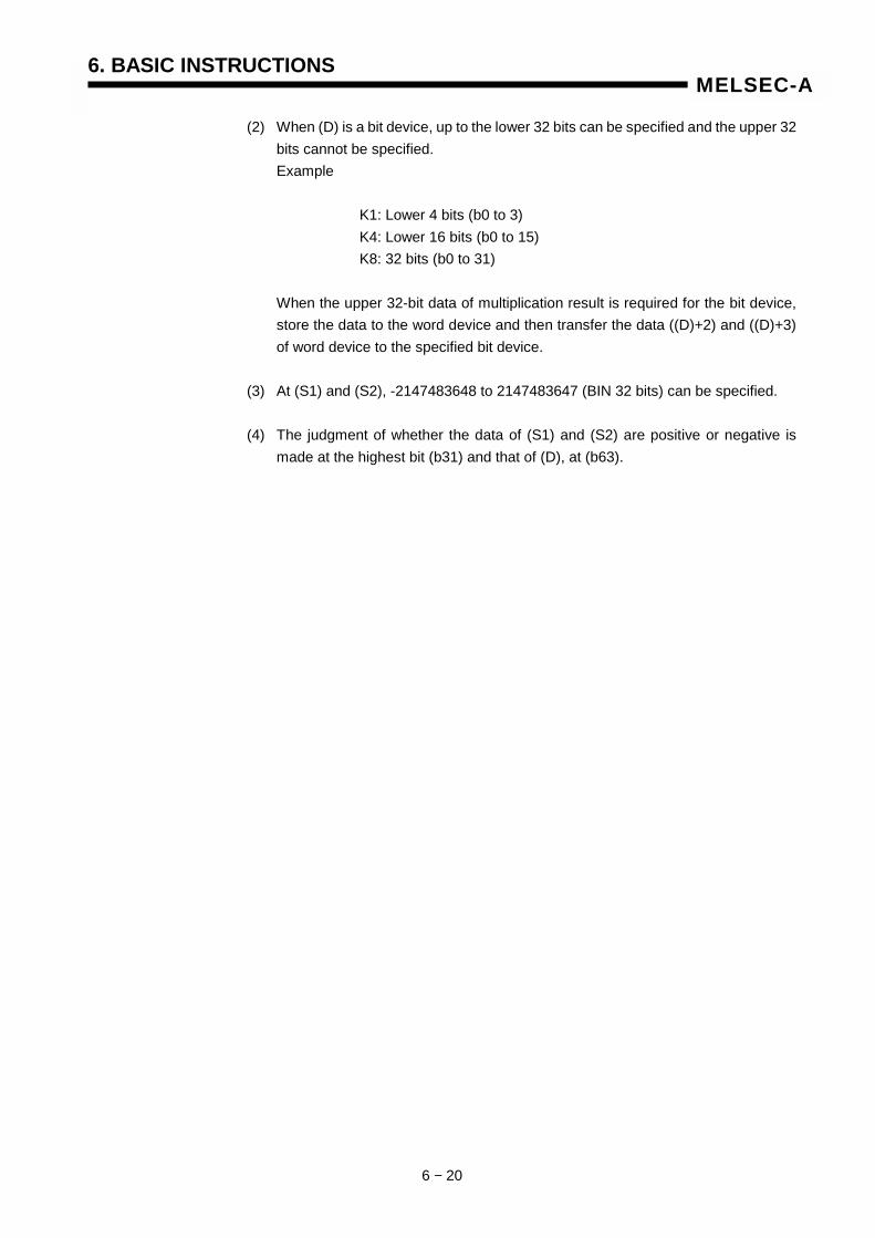
6. BASIC INSTRUCTIONS
6 − 20
MELSEC-A
(2) When (D) is a bit device, up to the lower 32 bits can be specified and the upper 32 bits cannot be specified.
Example
K1: Lower 4 bits (b0 to 3) K4: Lower 16 bits (b0 to 15) K8: 32 bits (b0 to 31)
When the upper 32-bit data of multiplication result is required for the bit device, store the data to the word device and then transfer the data ((D)+2) and ((D)+3) of word device to the specified bit device.
(3) At (S1) and (S2), -2147483648 to 2147483647 (BIN 32 bits) can be specified.
(4) The judgment of whether the data of (S1) and (S2) are positive or negative is made at the highest bit (b31) and that of (D), at (b63).
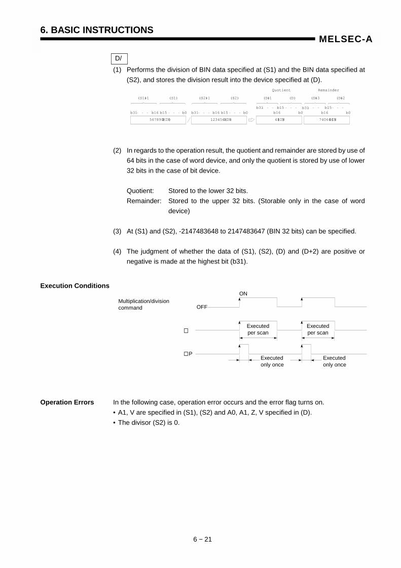
6. BASIC INSTRUCTIONS
6 − 21
MELSEC-A
D/ (1) Performs the division of BIN data specified at (S1) and the BIN data specified at
(S2), and stores the division result into the device specified at (D).
(2) In regards to the operation result, the quotient and remainder are stored by use of 64 bits in the case of word device, and only the quotient is stored by use of lower 32 bits in the case of bit device.
Quotient: Stored to the lower 32 bits. Remainder: Stored to the upper 32 bits. (Storable only in the case of word
device)
(3) At (S1) and (S2), -2147483648 to 2147483647 (BIN 32 bits) can be specified.
(4) The judgment of whether the data of (S1), (S2), (D) and (D+2) are positive or negative is made at the highest bit (b31).
Execution Conditions
Operation Errors In the following case, operation error occurs and the error flag turns on. • A1, V are specified in (S1), (S2) and A0, A1, Z, V specified in (D). • The divisor (S2) is 0.
74066( BIN)4(BIN)567890(BIN)
b31 b16
(S1)+1 (S1)
b15 b0
123456(BIN)
b31 b16
(S2)+1 (S2)
b15 b0b31
(D)+1 (D)
b15 b31
(D)+3
b15
Quotient Remainder
b16 b0 b16 b0
(D)+2
OFF
ON
Executed per scan
Executed per scan
Executed only once
Executed only once
P
Multiplication/division command
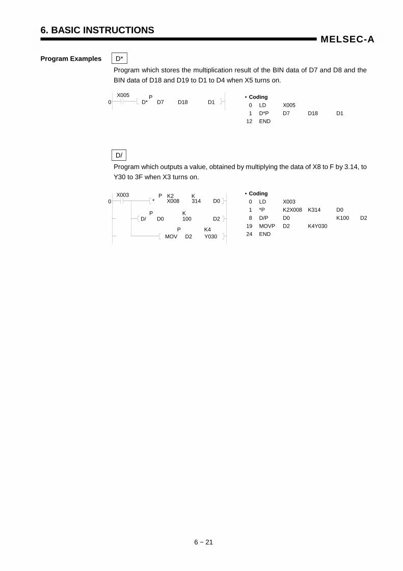
6. BASIC INSTRUCTIONS
6 − 21
MELSEC-A
Program Examples D* Program which stores the multiplication result of the BIN data of D7 and D8 and the BIN data of D18 and D19 to D1 to D4 when X5 turns on.
D/ Program which outputs a value, obtained by multiplying the data of X8 to F by 3.14, to Y30 to 3F when X3 turns on.
X005 D* D7 D18 D1 0
P • Coding 0 LD X005 1 D*P D7 D18 D1 12 END
• Coding 0 LD X003 1 *P K2X008 K314 D0 8 D/P D0 K100 D2 19 MOVP D2 K4Y030 24 END MOV D2 Y030
* X008 314 D0
D/ D0 100 D2
P K2 K
P
P K4
0 X003
K
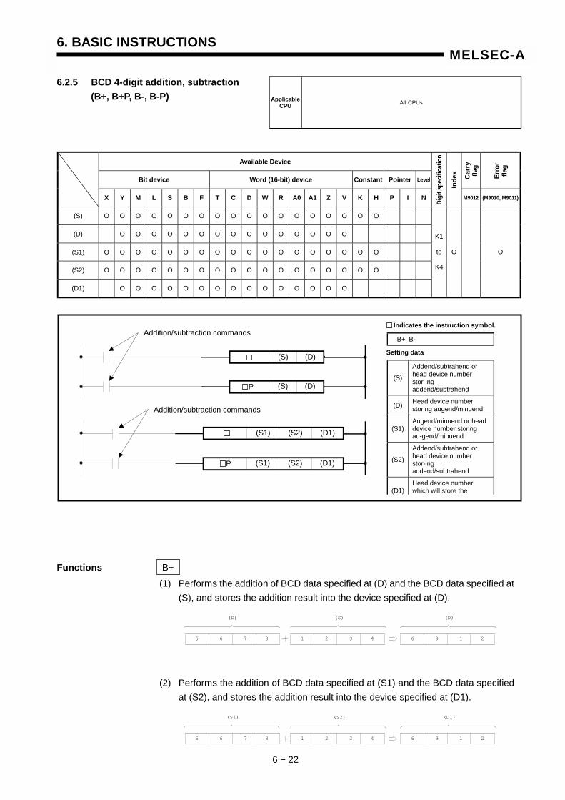
6. BASIC INSTRUCTIONS
6 − 22
MELSEC-A
6.2.5 BCD 4-digit addition, subtraction (B+, B+P, B-, B-P)
Available Device
Bit device Word (16-bit) device Constant Pointer Level Car
ry
flag
Erro
r fla
g
X Y M L S B F T C D W R A0 A1 Z V K H P I N Digi
t spe
cific
atio
n
Inde
x
M9012 (M9010, M9011)
(S) O O O O O O O O O O O O O O O O O O
(D) O O O O O O O O O O O O O O O
(S1) O O O O O O O O O O O O O O O O O O
(S2) O O O O O O O O O O O O O O O O O O
(D1) O O O O O O O O O O O O O O O
K1
to
K4
O O
Functions B+ (1) Performs the addition of BCD data specified at (D) and the BCD data specified at
(S), and stores the addition result into the device specified at (D).
(2) Performs the addition of BCD data specified at (S1) and the BCD data specified at (S2), and stores the addition result into the device specified at (D1).
Applicable CPU All CPUs
(S) (D)
(S) (D) P
Addition/subtraction commands
(S)
Addend/subtrahend or head device number stor-ing addend/subtrahend
(D) Head device number storing augend/minuend
(S1) Augend/minuend or head device number storing au-gend/minuend
(S2)
Addend/subtrahend or head device number stor-ing addend/subtrahend
(D1) Head device number which will store the
Setting data
B+, B-
Indicates the instruction symbol.
Addition/subtraction commands
(S1) (D1)
(S1) (D1) P
(S2)
(S2)
(D)
5 6 7 8
(S) (D)
1 2 3 4 6 9 1 2
(S1)
5 6 7 8
(S2) (D1)
1 2 3 4 6 9 1 2
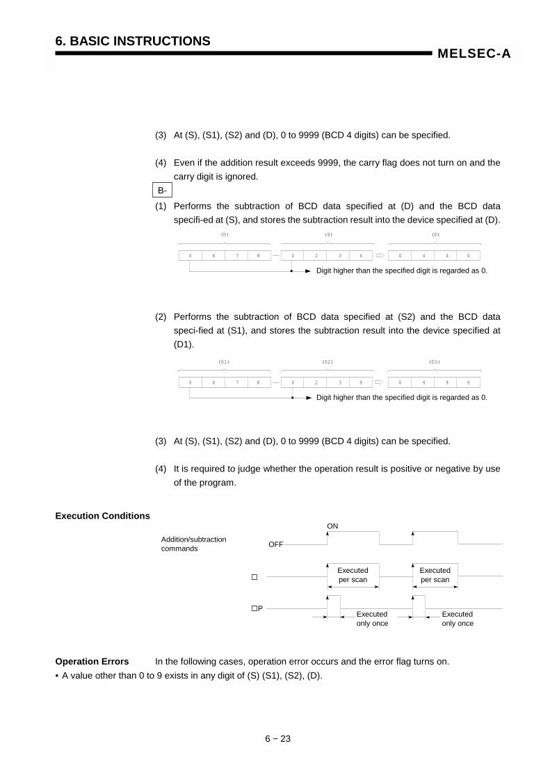
6. BASIC INSTRUCTIONS
6 − 23
MELSEC-A
(3) At (S), (S1), (S2) and (D), 0 to 9999 (BCD 4 digits) can be specified. (4) Even if the addition result exceeds 9999, the carry flag does not turn on and the
carry digit is ignored. B-
(1) Performs the subtraction of BCD data specified at (D) and the BCD data specifi-ed at (S), and stores the subtraction result into the device specified at (D).
(2) Performs the subtraction of BCD data specified at (S2) and the BCD data speci-fied at (S1), and stores the subtraction result into the device specified at (D1).
(3) At (S), (S1), (S2) and (D), 0 to 9999 (BCD 4 digits) can be specified. (4) It is required to judge whether the operation result is positive or negative by use
of the program.
Execution Conditions
Operation Errors In the following cases, operation error occurs and the error flag turns on. • A value other than 0 to 9 exists in any digit of (S) (S1), (S2), (D).
(D)
0 6 7 8
(S) (D)
0 2 3 4 0 4 4 4
Digit higher than the specified digit is regarded as 0.
(S1)
0 6 7 8
(S2) (D1)
0 2 3 4 0 4 4 4
Digit higher than the specified digit is regarded as 0.
OFF
ON
Executed per scan
Executed per scan
Executed only once
Executed only once
P
Addition/subtraction commands
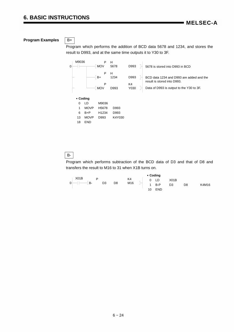
6. BASIC INSTRUCTIONS
6 − 24
MELSEC-A
Program Examples B+ Program which performs the addition of BCD data 5678 and 1234, and stores the result to D993, and at the same time outputs it to Y30 to 3F.
B-
Program which performs subtraction of the BCD data of D3 and that of D8 and transfers the result to M16 to 31 when X1B turns on.
•••• Coding 0 LD M9036 1 MOVP H5678 D993 6 B+P H1234 D993 13 MOVP D993 K4Y030 18 END
0 M9036
P H B+ 1234 D993
P H MOV 5678 D993
P K4 MOV D993 Y030
5678 is stored into D993 in BCD
BCD data 1234 and D993 are added and the result is stored into D993.
Data of D993 is output to the Y30 to 3F.
0 X01B P K4
B- D3 D8 M16
•••• Coding 0 LD X01B 1 B-P D3 D8 K4M16 10 END
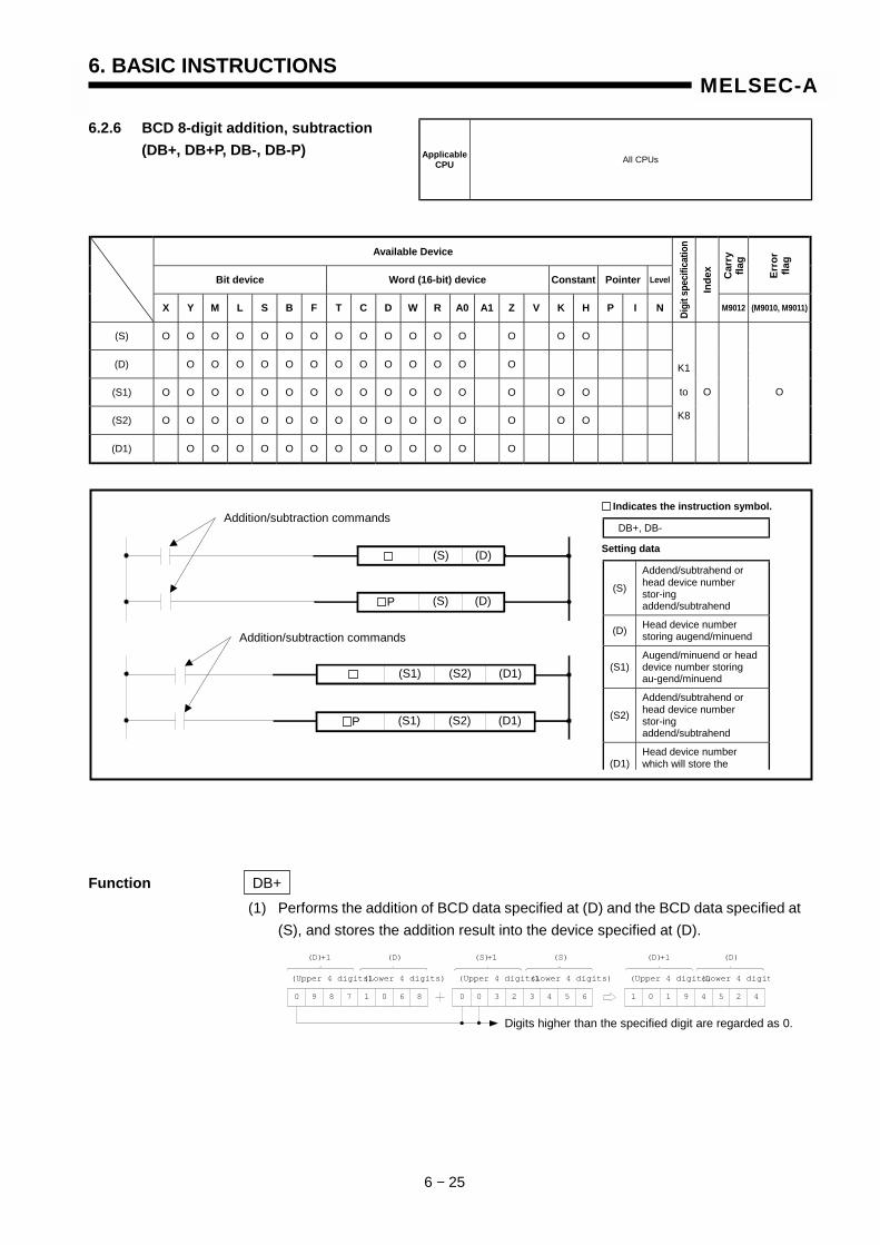
6. BASIC INSTRUCTIONS
6 − 25
MELSEC-A
6.2.6 BCD 8-digit addition, subtraction (DB+, DB+P, DB-, DB-P)
Available Device
Bit device Word (16-bit) device Constant Pointer Level Car
ry
flag
Erro
r fla
g
X Y M L S B F T C D W R A0 A1 Z V K H P I N Digi
t spe
cific
atio
n
Inde
x
M9012 (M9010, M9011)
(S) O O O O O O O O O O O O O O O O
(D) O O O O O O O O O O O O O
(S1) O O O O O O O O O O O O O O O O
(S2) O O O O O O O O O O O O O O O O
(D1) O O O O O O O O O O O O O
K1
to
K8
O O
Function DB+ (1) Performs the addition of BCD data specified at (D) and the BCD data specified at
(S), and stores the addition result into the device specified at (D).
Applicable CPU All CPUs
(S) (D)
(S) (D) P
Addition/subtraction commands
(S)
Addend/subtrahend or head device number stor-ing addend/subtrahend
(D) Head device number storing augend/minuend
(S1) Augend/minuend or head device number storing au-gend/minuend
(S2)
Addend/subtrahend or head device number stor-ing addend/subtrahend
(D1) Head device number which will store the
Setting data
DB+, DB-
Indicates the instruction symbol.
Addition/subtraction commands
(S1) (D1)
(S1) (D1) P
(S2)
(S2)
0 9 8 7 1 0 6 8 0 0 3 2 3 4 5 6 1 0 1 9 4 5 2 4
(D)+1 (D) (S)+1 (S) (D)+1 (D)
(Upper 4 digits) (Upper 4 digits) (Upper 4 digits)(Lower 4 digits) (Lower 4 digits) (Lower 4 digit
Digits higher than the specified digit are regarded as 0.
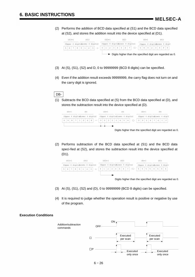
6. BASIC INSTRUCTIONS
6 − 26
MELSEC-A
(2) Performs the addition of BCD data specified at (S1) and the BCD data specified at (S2), and stores the addition result into the device specified at (D1).
(3) At (S), (S1), (S2) and D, 0 to 99999999 (BCD 8 digits) can be specified. (4) Even if the addition result exceeds 99999999, the carry flag does not turn on and
the carry digit is ignored.
DB- (1) Subtracts the BCD data specified at (S) from the BCD data specified at (D), and
stores the subtraction result into the device specified at (D).
(2) Performs subtraction of the BCD data specified at (S1) and the BCD data speci-fied at (S2), and stores the subtraction result into the device specified at (D1).
(3) At (S), (S1), (S2) and (D), 0 to 99999999 (BCD 8 digits) can be specified. (4) It is required to judge whether the operation result is positive or negative by use
of the program.
Execution Conditions
5 6 7 8 9 1 2 3 0 1 2 3 4 5 6 5 5 5 5 4 5 5 6
(S1)+1 (S1) (S2)+1 (S2) (D)+1 (D1)
(Upper 4 digits) (Upper 4 digits) (Upper 4 digits)(Lower 4 digits) (Lower 4 digits) (Lower 4 digit
7
5 6 7 8 9 1 2 3 0 1 2 3 4 5 6 5 8 0 2 3 6 9 0
(S1)+1 (S1) (S2)+1 (S2) (D)+1 (D1)
(Upper 4 digits) (Upper 4 digits) (Upper 4 digits)(Lower 4 digits) (Lower 4 digits) (Lower 4 digit
7
Digits higher than the specified digit are regarded as 0.
0 9 8 7 1 0 6 8 0 0 3 2 3 4 5 6 0 9 5 4 7 6 1 2
(D)+1 (D) (S)+1 (S) (D)+1 (D)
(Upper 4 digits) (Upper 4 digits) (Upper 4 digits)(Lower 4 digits) (Lower 4 digits) (Lower 4 digit
Digits higher than the specified digit are regarded as 0.
Digits higher than the specified digit are regarded as 0.
OFF
ON
Executed per scan
Executed per scan
Executed only once
Executed only once
P
Addition/subtraction commands
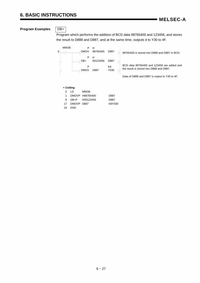
6. BASIC INSTRUCTIONS
6 − 27
MELSEC-A
Program Examples DB+ Program which performs the addition of BCD data 98765400 and 123456, and stores the result to D888 and D887, and at the same time, outputs it to Y30 to 4F.
•••• Coding 0 LD M9036 1 DMOVP H98765400 D887 8 DB+P H00123456 D887 17 DMOVP D887 K8Y030 24 END
0 M9036
P H DB+ 00123456 D887
P H DMOV 98765400 D887
P K8 DMOV D887 Y030
98765400 is stored into D888 and D887 in BCD.
BCD data 98765400 and 123456 are added and the result is stored into D888 and D887.
Data of D888 and D887 is output to Y30 to 4F.
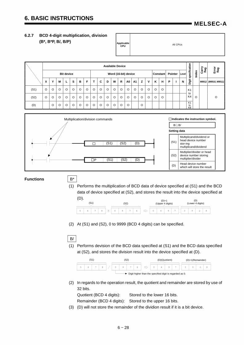
6. BASIC INSTRUCTIONS
6 − 28
MELSEC-A
6.2.7 BCD 4-digit multiplication, division (B*, B*P, B/, B/P)
Available Device
Bit device Word (16-bit) device Constant Pointer Level Car
ry
flag
Erro
r fla
g
X Y M L S B F T C D W R A0 A1 Z V K H P I N Digi
t spe
cific
atio
n
Inde
x
M9012 (M9010, M9011)
(S1) O O O O O O O O O O O O O O O O O O
(S2) O O O O O O O O O O O O O O O O O O
K1 to K4
(D) O O O O O O O O O O O O O
O O
Functions B* (1) Performs the multiplication of BCD data of device specified at (S1) and the BCD
data of device specified at (S2), and stores the result into the device specified at (D).
(2) At (S1) and (S2), 0 to 9999 (BCD 4 digits) can be specified.
B/ (1) Performs devision of the BCD data specified at (S1) and the BCD data specified
at (S2), and stores the division result into the device specified at (D).
(2) In regards to the operation result, the quotient and remainder are stored by use of 32 bits.
Quotient (BCD 4 digits): Stored to the lower 16 bits. Remainder (BCD 4 digits): Stored to the upper 16 bits. (3) (D) will not store the remainder of the dividion result if it is a bit device.
Applicable CPU All CPUs
K1 to K8
0 8 7 6 0 4 9 7 3 9 2 85 6 7 8
(S1) (S2) (D)+1
(Upper 4 digits) (D)
(Lower 4 digits)
0 8 7 6 0 4 9 7 3 9 2 85 6 7 8
(S1) (S2) (D)(Quotient) (D)+1(Remainder)
Digit higher than the specified digit is regarded as 0.
Multiplication/division commands
(S1) (S2) (D)
(S1) (S2) (D) P
(S1)
Multiplicand/dividend or head device number stor-ing multiplicand/dividend
(S2) Multiplier/divider or head device number storing multiplier/divider
(D) Head device number which will store the result
Setting data
B∗ , B/
Indicates the instruction symbol.
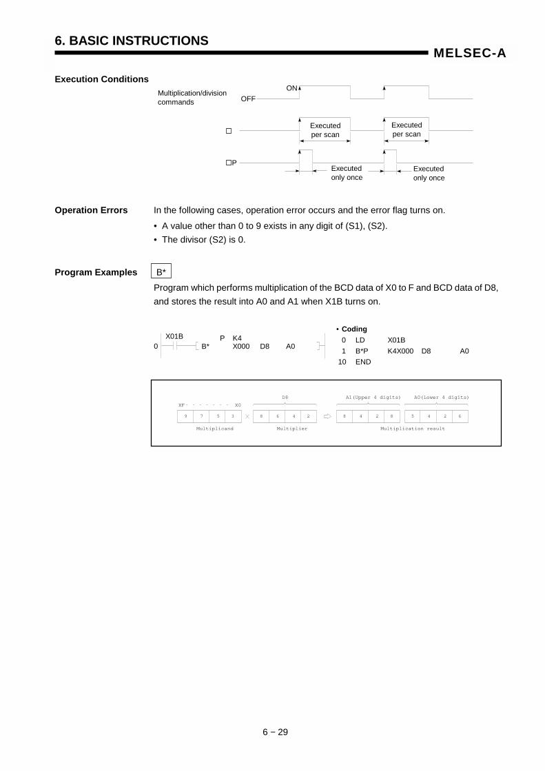
6. BASIC INSTRUCTIONS
6 − 29
MELSEC-A
Execution Conditions
Operation Errors In the following cases, operation error occurs and the error flag turns on.
• A value other than 0 to 9 exists in any digit of (S1), (S2). • The divisor (S2) is 0.
Program Examples B* Program which performs multiplication of the BCD data of X0 to F and BCD data of D8, and stores the result into A0 and A1 when X1B turns on.
• Coding 0 LD X01B 1 B*P K4X000 D8 A0 10 END
0X01B P K4
B* X000 D8 A0
D8 A1(Upper 4 digits)
8 6 4 2 8 4 2 8 5 4 2 69 5 3
A0(Lower 4 digits)
Multiplicand
XF X0
7
Multiplier Multiplication result
OFF
ON
Multiplication/division commands
Executed per scan
Executed per scan
Executed only once
Executed only once
P
OFF ON
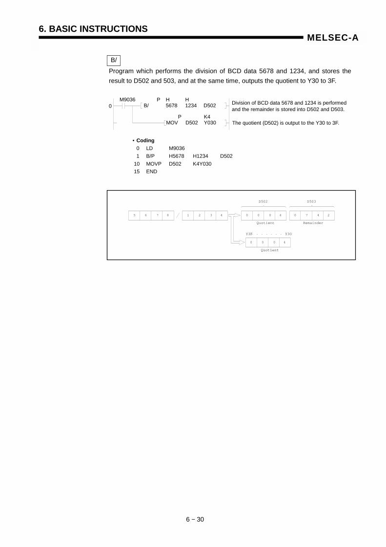
6. BASIC INSTRUCTIONS
6 − 30
MELSEC-A
B/ Program which performs the division of BCD data 5678 and 1234, and stores the result to D502 and 503, and at the same time, outputs the quotient to Y30 to 3F.
Division of BCD data 5678 and 1234 is performedand the remainder is stored into D502 and D503.
P H H B/ 5678 1234 D502
P K4 MOV D502 Y030
0 M9036
The quotient (D502) is output to the Y30 to 3F.
• Coding 0 LD M9036 1 B/P H5678 H1234 D502 10 MOVP D502 K4Y030 15 END
D502
1 2 3 4 0 0 0 4 0 7 4 25 7 8
D503
Y3F Y3O
6
Quotient
0 0 0 4
Remainder
Quotient
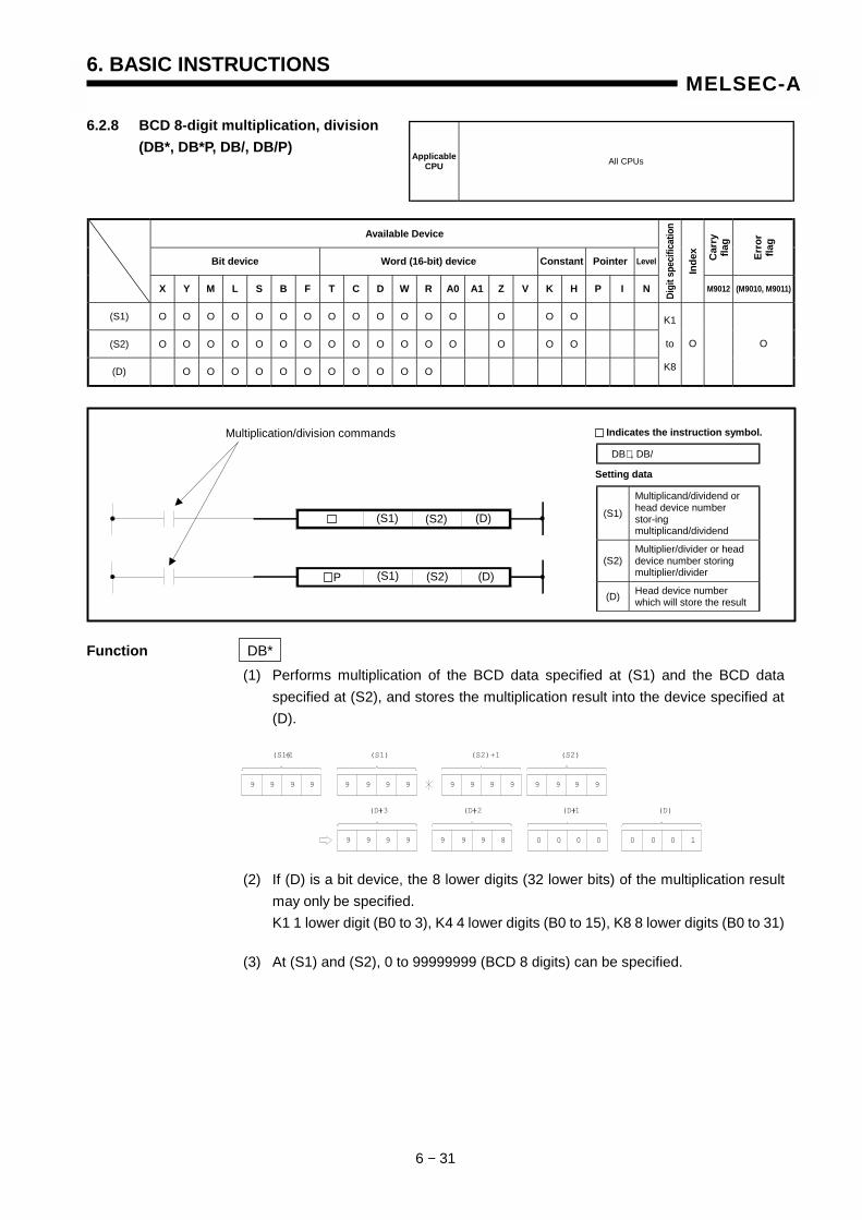
6. BASIC INSTRUCTIONS
6 − 31
MELSEC-A
6.2.8 BCD 8-digit multiplication, division (DB*, DB*P, DB/, DB/P)
Available Device
Bit device Word (16-bit) device Constant Pointer Level Car
ry
flag
Erro
r fla
g
X Y M L S B F T C D W R A0 A1 Z V K H P I N Digi
t spe
cific
atio
n
Inde
x
M9012 (M9010, M9011)
(S1) O O O O O O O O O O O O O O O O
(S2) O O O O O O O O O O O O O O O O
(D) O O O O O O O O O O O
K1
to
K8
O O
Function DB* (1) Performs multiplication of the BCD data specified at (S1) and the BCD data
specified at (S2), and stores the multiplication result into the device specified at (D).
(2) If (D) is a bit device, the 8 lower digits (32 lower bits) of the multiplication result may only be specified.
K1 1 lower digit (B0 to 3), K4 4 lower digits (B0 to 15), K8 8 lower digits (B0 to 31)
(3) At (S1) and (S2), 0 to 99999999 (BCD 8 digits) can be specified.
Applicable CPU All CPUs
(S1)+1 (S1)
99 9 999 9 9 99 9 9 99 9 9
(S2)+1 (S2)
(D)+3 (D)+2 (D)+1 (D)
89 9 999 9 9 00 0 0 10 0 0
Multiplication/division commands
(S1) (S2) (D)
(S1) (S2) (D) P
(S1)
Multiplicand/dividend or head device number stor-ing multiplicand/dividend
(S2) Multiplier/divider or head device number storing multiplier/divider
(D) Head device number which will store the result
Setting data
DB∗ , DB/
Indicates the instruction symbol.
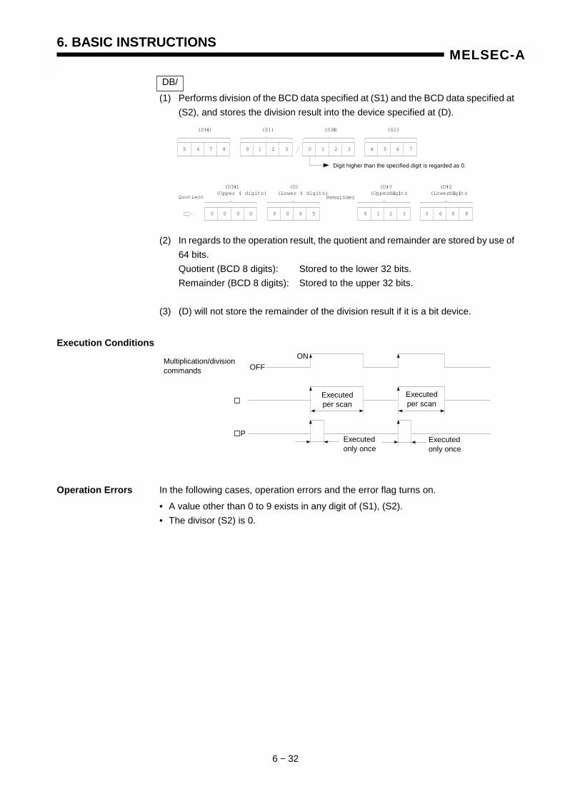
6. BASIC INSTRUCTIONS
6 − 32
MELSEC-A
DB/ (1) Performs division of the BCD data specified at (S1) and the BCD data specified at
(S2), and stores the division result into the device specified at (D).
(2) In regards to the operation result, the quotient and remainder are stored by use of 64 bits.
Quotient (BCD 8 digits): Stored to the lower 32 bits. Remainder (BCD 8 digits): Stored to the upper 32 bits. (3) (D) will not store the remainder of the division result if it is a bit device.
Execution Conditions
Operation Errors In the following cases, operation errors and the error flag turns on.
• A value other than 0 to 9 exists in any digit of (S1), (S2). • The divisor (S2) is 0.
(D1)+1(Upper 4 digits)
(D)(Lower 4 digits)
(D)+3(Upper 4 digits)
(D)+2(Lower 4 digits)
50 0 400 0 0 30 1 2 83 6 0
Quotient Remainder
(S1)+1 (S1) (S2)+1 (S2)
39 1 285 6 7 30 1 2 74 5 6
Digit higher than the specified digit is regarded as 0.
OFF
ON
Multiplication/division commands
Executed per scan
Executed per scan
Executed only once
Executed only once
P
OFF ON
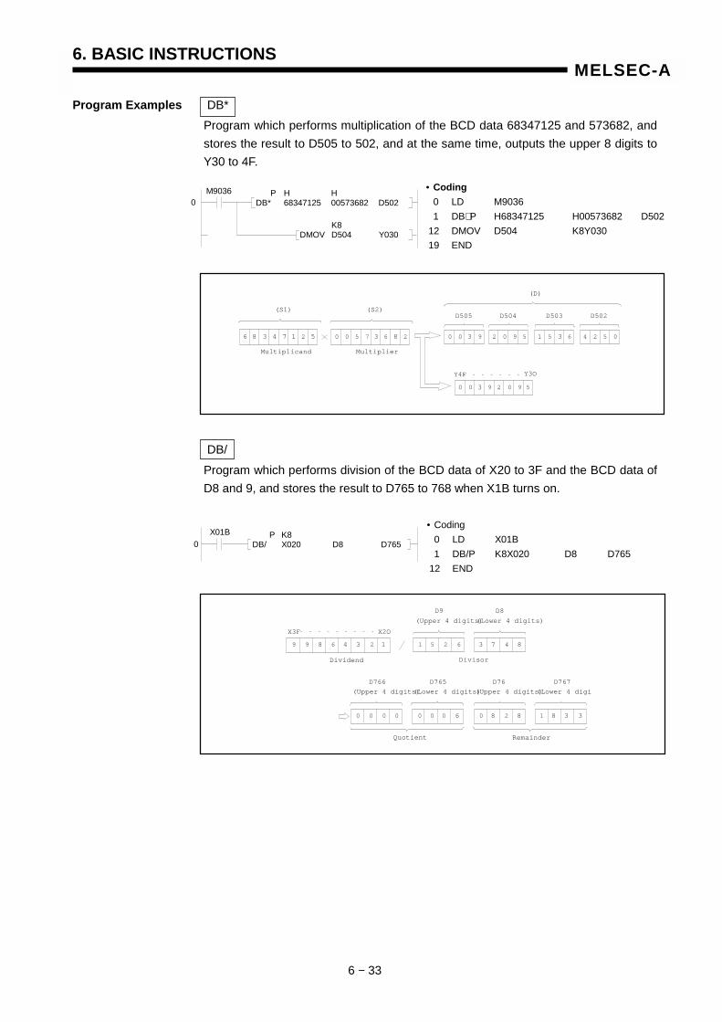
6. BASIC INSTRUCTIONS
6 − 33
MELSEC-A
Program Examples DB* Program which performs multiplication of the BCD data 68347125 and 573682, and stores the result to D505 to 502, and at the same time, outputs the upper 8 digits to Y30 to 4F.
DB/ Program which performs division of the BCD data of X20 to 3F and the BCD data of D8 and 9, and stores the result to D765 to 768 when X1B turns on.
0 0 5 6
9
7 22
D505
Y4F Y3O
6 8 4 7 13 5
D504 D503 D502
83
0 0 3 2 0 9 5
90 0 3 2 0 9 5 61 5 3 4 2 5 0
(S1) (S2)
(D)
Multiplicand Multiplier
M9036 0
P H H DB* 68347125 00573682 D502
K8 DMOV D504 Y030
• Coding 0 LD M9036 1 DB∗ P H68347125 H00573682 D502 12 DMOV D504 K8Y030 19 END
P K8 DB/ X020 D8 D765
X01B 0
• Coding 0 LD X01B 1 DB/P K8X020 D8 D765 12 END
0
6
2
2
X3F X2O
6 8
4 71
3
(Upper 4 digits)
8
3 61 5
D766
9
0 0
329
1
4
(Upper 4 digits)
(Upper 4 digits)(Lower 4 digits)
(Lower 4 digits)
(Lower 4 digi
D765 D76 D767
D9 D8
0 0 0 0 0 8 3
8 8
Dividend Divisor
Quotient Remainder
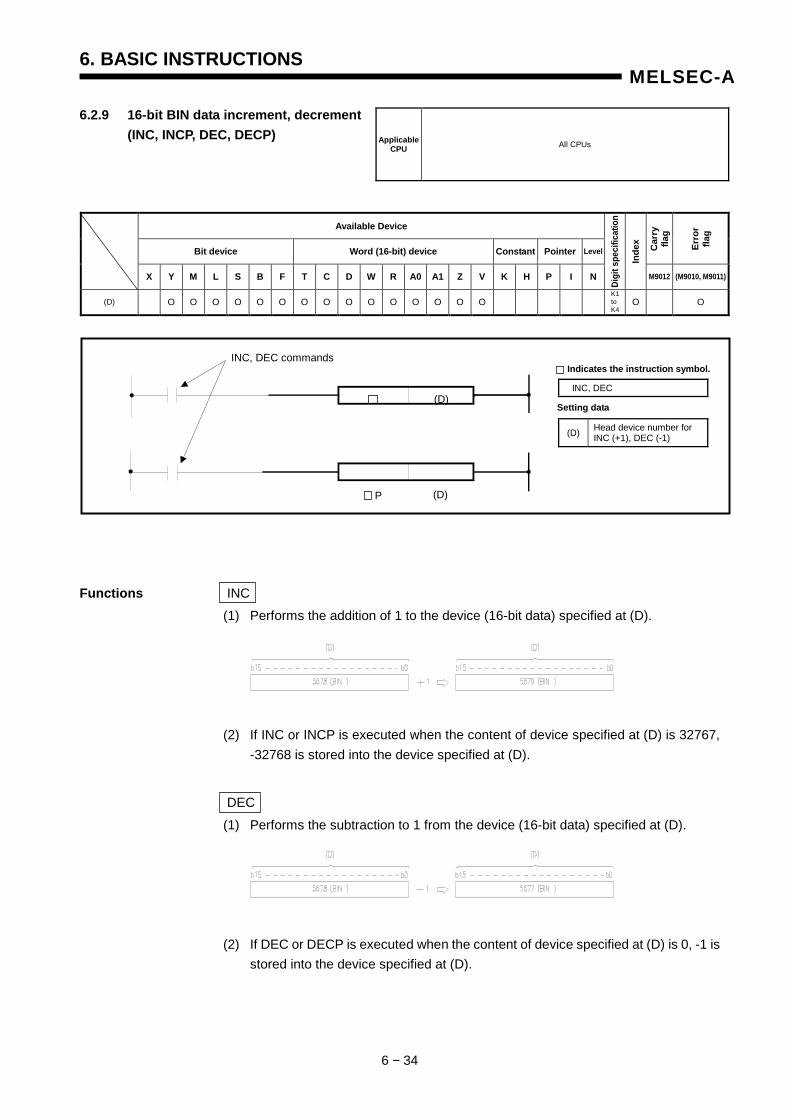
6. BASIC INSTRUCTIONS
6 − 34
MELSEC-A
6.2.9 16-bit BIN data increment, decrement (INC, INCP, DEC, DECP)
Available Device
Bit device Word (16-bit) device Constant Pointer Level Car
ry
flag
Erro
r fla
g
X Y M L S B F T C D W R A0 A1 Z V K H P I N
Digi
t spe
cific
atio
n
Inde
x
M9012 (M9010, M9011)
(D) O O O O O O O O O O O O O O O O O
Functions INC (1) Performs the addition of 1 to the device (16-bit data) specified at (D).
(2) If INC or INCP is executed when the content of device specified at (D) is 32767, -32768 is stored into the device specified at (D).
DEC (1) Performs the subtraction to 1 from the device (16-bit data) specified at (D).
(2) If DEC or DECP is executed when the content of device specified at (D) is 0, -1 is stored into the device specified at (D).
Applicable CPU All CPUs
INC, DEC commands
K1 to K4
(D)
(D)
(D) Head device number for INC (+1), DEC (-1)
Setting data
INC, DEC
Indicates the instruction symbol.
P
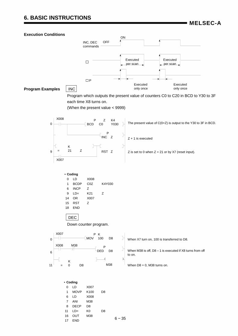
6. BASIC INSTRUCTIONS
6 − 35
MELSEC-A
Execution Conditions Program Examples INC
Program which outputs the present value of counters C0 to C20 in BCD to Y30 to 3F each time X8 turns on. (When the present value < 9999)
DEC Down counter program.
INC, DEC commands
Executed per scan
Executed per scan
Executed only once
The present value of C(0+Z) is output to the Y30 to 3F in BCD.X008 P Z K4
BCD C0 Y030 0
P INC Z Z + 1 is executed
K = 21 Z 9 Z is set to 0 when Z = 21 or by X7 (reset input).
X007
• Coding 0 LD X008 1 BCDP C0Z K4Y030 6 INCP Z 9 LD= K21 Z 14 OR X007 15 RST Z 18 END
RST Z
( )
X007
0
6
P K MOV 100 D8 When X7 turn on, 100 is transferred to D8.
X008
11
M38 P DED D8
K = 0 D8
When M38 is off, D8 – 1 is executed if X8 turns from offto on.
M38 When D8 = 0, M38 turns on.
• Coding 0 LD X007 1 MOVP K100 D8 6 LD X008 7 ANI M38 8 DECP D8 11 LD= K0 D8 16 OUT M38 17 END
P
ON OFF
Executed only once
6. BASIC INSTRUCTIONS
6 − 36
MELSEC-A
6.2.10 32-bit BIN data increment, decrement
(DINC, DINCP, DDEC, DDECP)
Available Device
Bit device Word (16-bit) device Constant Pointer Level Car
ry
flag
Erro
r fla
g
X Y M L S B F T C D W R A0 A1 Z V K H P I N
Digi
t spe
cific
atio
n
Inde
x
M9012 (M9010, M9011)
(D) O O O O O O O O O O O O O O O O O
Functions DINC (1) Performs the addition of 1 to the device (32-bit data) specified at (D).
(2) If DINC or DINCP is executed when the content of device specified at (D) is 2147483647, - 2147483648 is stored into the device specified at (D)
DDEC
(1) Performs the subtraction of 1 from the device (32-bit data) specified at (D).
(2) If DDEC or DDECP is executed when the content of device specified at (D) is 0, - 1is stored into the device specified at (D).
Applicable CPU All CPUs
K1 to K8
DINC, DDEC commands
(D)
(D)
(D) Head device number for DINC (+1), DDEC(-1)
Setting data
DINC, DDEC
Indicates the instruction symbol.
P
6. BASIC INSTRUCTIONS
6 − 37
MELSEC-A
Execution Conditions Program Examples DINC
(1) Program which adds 1 to the data of D0 and 1when X0 turns on.
(2) Program which adds 1 to the data of X10 to 27 and stores the result to D3 and 4 when X0 turns on.
DDEC (1) Program which subtracts 1 from the data of D0 and 1 when X0 turns on.
(2) Program which subtracts 1 from the data of X10 to 27 and stores the result to D3 and 4 when X0 turns on.
DINC, DDEC commands
Executed per scan
Executed per scan
Executed only once
X000 0
P DINC DO
• Coding 0 LD X000 1 DINCP D0 4 END
• Coding 0 LD X000 1 DMOVP K6X010 D3 8 DINCP D3 11 END
X000 0
P K6 DMOV X010 D3
P DINC D3
X000 0
P DDEC D0
• Coding 0 LD X000 1 DDECP D0 4 END
• Coding 0 LD X000 1 DMOVP K6X010 D3 8 DDECP D3 11 END
X000 0
P K6 DMOV X010 D3
P DDEC D3
P
Executed only once
ON OFF
6. BASIC INSTRUCTIONS
6 − 38
MELSEC-A
6.3 BCD ↔↔↔↔ BIN Conversion Instructions
The BCD ↔ BIN conversion instructions are instructions which convert BCD data to BIN data and BCD data.
Classification Instruction Symbol Ref. Page Classification Instruction
symbol Ref. Page
BCD 6-39 BIN 6-42
BCDP 6-39 BINP 6-42
DBCD 6-39 DBIN 6-42 BDC
DBCDP 6-39
BIN
DBINP 6-42
Numeric values usable for the BCD ↔ BIN conversion instructions are as follows:
BCD, BCDP, BIN, BINP: 0 to 9999 DBCD, DBCDP, DBIN, DBINP: 0 to 99999999
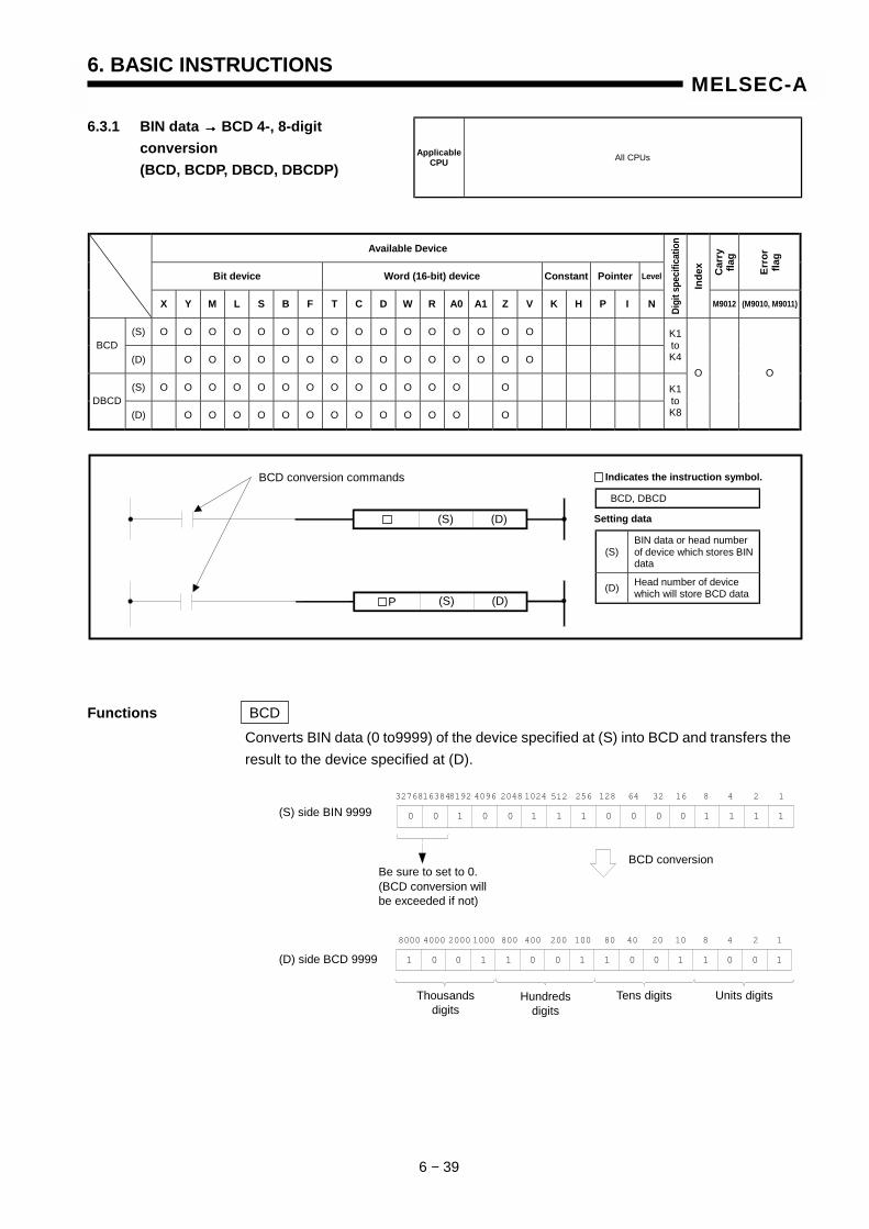
6. BASIC INSTRUCTIONS
6 − 39
MELSEC-A
6.3.1 BIN data →→→→ BCD 4-, 8-digit conversion (BCD, BCDP, DBCD, DBCDP)
Available Device
Bit device Word (16-bit) device Constant Pointer Level Car
ry
flag
Erro
r fla
g
X Y M L S B F T C D W R A0 A1 Z V K H P I N Digi
t spe
cific
atio
n
Inde
x
M9012 (M9010, M9011)
(S) O O O O O O O O O O O O O O O O BCD
(D) O O O O O O O O O O O O O O O
K1 to K4
(S) O O O O O O O O O O O O O O DBCD
(D) O O O O O O O O O O O O O
K1 to K8
O O
Functions BCD Converts BIN data (0 to9999) of the device specified at (S) into BCD and transfers the result to the device specified at (D).
Applicable CPU All CPUs
(S) (D)
(S) (D) P
BCD conversion commands
(S) BIN data or head number of device which stores BIN data
(D) Head number of device which will store BCD data
Setting data
BCD, DBCD
Indicates the instruction symbol.
32768163848192 4096
0 0 1 0 0 1 1 1 0 0 0 0 1 1 1 1
2048 1024 512 256 128 64 32 16 8 4 2 1
8000 4000 2000 1000 800 400 200 100 80 40 20 10 8 4 2 1
1 0 0 0 01 1 1 1 0 0 01 1 10
Be sure to set to 0. (BCD conversion will be exceeded if not)
(S) side BIN 9999
(D) side BCD 9999
BCD conversion
Units digits Tens digits Hundreds digits
Thousands digits
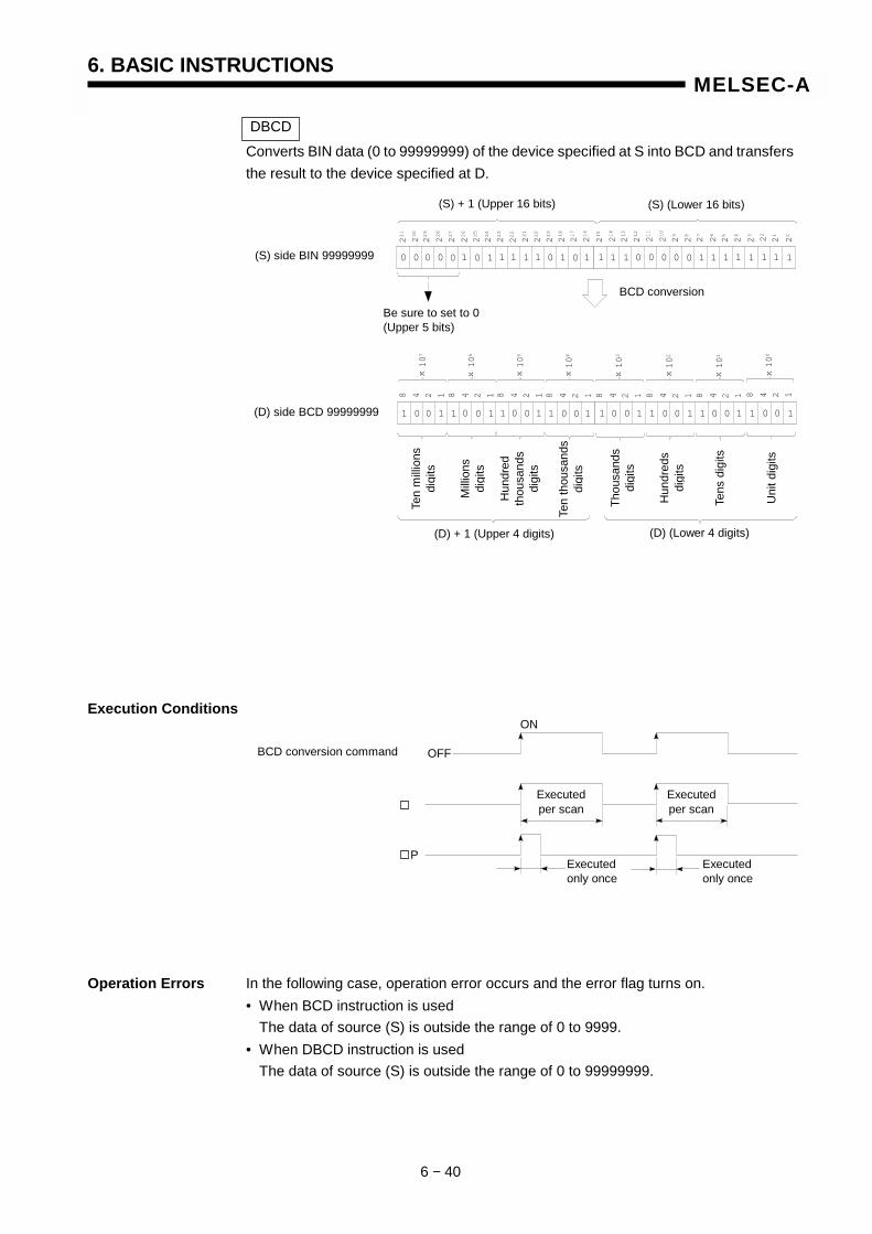
6. BASIC INSTRUCTIONS
6 − 40
MELSEC-A
DBCD Converts BIN data (0 to 99999999) of the device specified at S into BCD and transfers the result to the device specified at D.
Execution Conditions
Operation Errors In the following case, operation error occurs and the error flag turns on. • When BCD instruction is used The data of source (S) is outside the range of 0 to 9999. • When DBCD instruction is used The data of source (S) is outside the range of 0 to 99999999.
0 00 01 1 10 0 1 11 10 10 11 1 0 0 00 0 1 11 11 1 11
230
229
224
221
223
225
226
227
228
220
222
231
219
210
211
212
213
214
215
216
217
218
26
29
20
2122
23
24
25
27
28
1 00 00 1 01 1 1 10 01 10 01 0 1 1 00 1 1 00 11 0 104 2
107
x
18 4 2106
18 4 2105
18 4 2104
18 4 2103
18 4 2102
18 4 2101
18 4 2100
18
x x x x x x x
Be sure to set to 0 (Upper 5 bits)
(S) side BIN 99999999
(D) side BCD 99999999
BCD conversion
Ten
milli
ons
digi
ts
(S) (Lower 16 bits) (S) + 1 (Upper 16 bits)
Milli
ons
digi
ts
Hun
dred
th
ousa
nds
digi
ts
Ten
thou
sand
s di
gits
Thou
sand
s di
gits
Hun
dred
s di
gits
Tens
dig
its
Uni
t dig
its
(D) (Lower 4 digits) (D) + 1 (Upper 4 digits)
OFF
ON
Executed per scan
Executed per scan
Executed only once
Executed only once
P
BCD conversion command
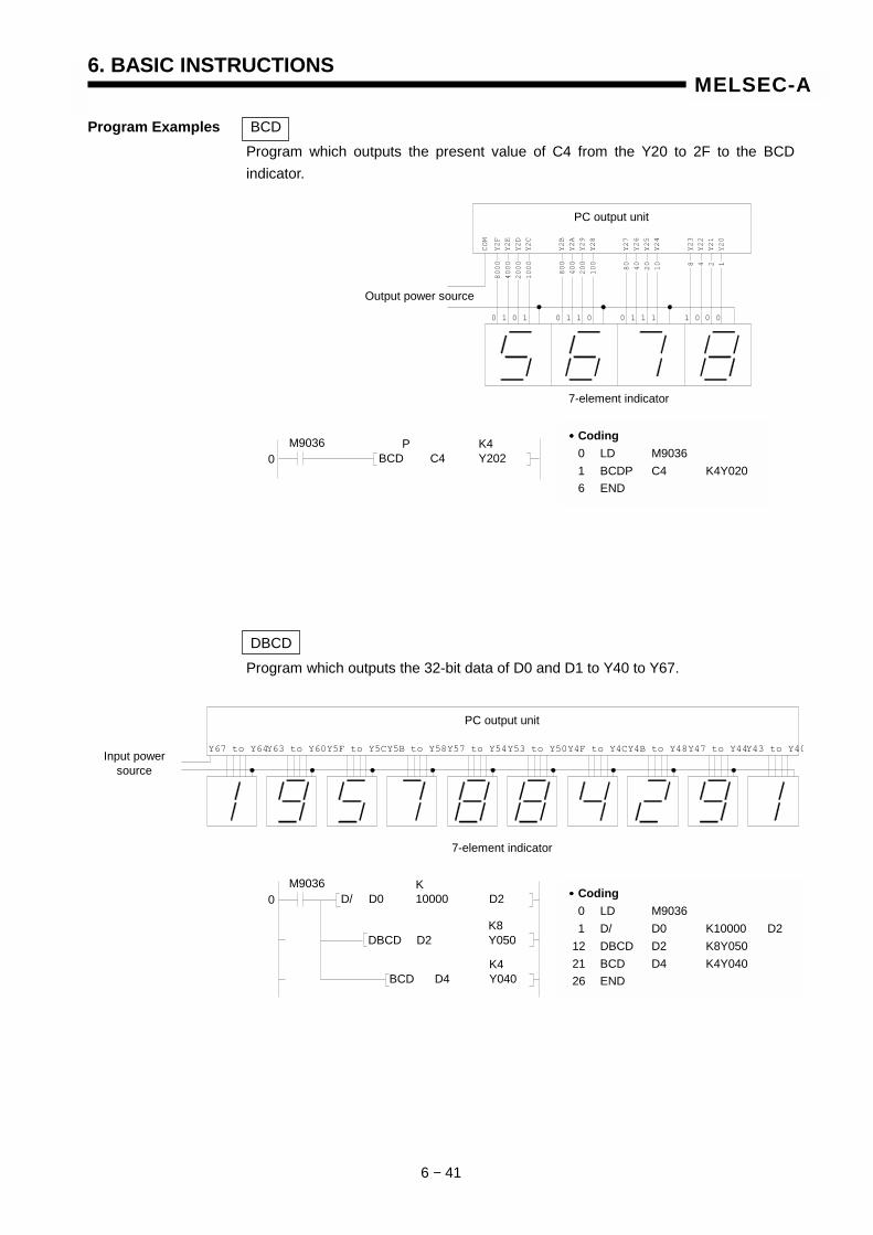
6. BASIC INSTRUCTIONS
6 − 41
MELSEC-A
Program Examples BCD Program which outputs the present value of C4 from the Y20 to 2F to the BCD indicator.
DBCD Program which outputs the 32-bit data of D0 and D1 to Y40 to Y67.
COM
Y2F
Y2E
Y2D
Y2C
Y2B
Y2A
Y29
Y28
Y27
Y26
Y25
Y24
Y23
Y22
Y21
Y20
8000
4000
2000
1000
800
400
200
100
80
40
20
10 8 4 2 1
0 1 0 1 0 1 1 0 0 1 1 1 1 0 0 0
PC output unit
Output power source
7-element indicator
•••• Coding 0 LD M9036 1 BCDP C4 K4Y020 6 END
0 P K4 BCD C4 Y202
M9036
Y67 to Y64Y63 to Y60Y5F to Y5CY5B to Y58Y57 to Y54Y53 to Y50Y4F to Y4CY4B to Y48Y47 to Y44Y43 to Y40
PC output unit
7-element indicator
Input power source
•••• Coding 0 LD M9036 1 D/ D0 K10000 D2 12 DBCD D2 K8Y050 21 BCD D4 K4Y040 26 END
0 K D/ D0 10000 D2
M9036
K8 DBCD D2 Y050
K4 BCD D4 Y040
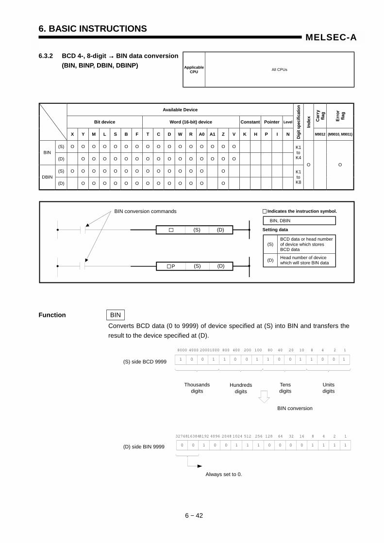
6. BASIC INSTRUCTIONS
6 − 42
MELSEC-A
6.3.2 BCD 4-, 8-digit →→→→ BIN data conversion (BIN, BINP, DBIN, DBINP)
Available Device
Bit device Word (16-bit) device Constant Pointer Level Car
ry
flag
Erro
r fla
g
X Y M L S B F T C D W R A0 A1 Z V K H P I N Digi
t spe
cific
atio
n
Inde
x
M9012 (M9010, M9011)
(S) O O O O O O O O O O O O O O O O BIN
(D) O O O O O O O O O O O O O O O
K1 to K4
(S) O O O O O O O O O O O O O O DBIN
(D) O O O O O O O O O O O O O
K1 to K8
O O
Function BIN Converts BCD data (0 to 9999) of device specified at (S) into BIN and transfers the result to the device specified at (D).
Applicable CPU All CPUs
(S) (D)
(S) (D) P
BIN conversion commands
(S) BCD data or head number of device which stores BCD data
(D) Head number of device which will store BIN data
Setting data
BIN, DBIN
Indicates the instruction symbol.
8000 4000 20001000 800 400 200 100 80 40 20 8 4 2 110
1 0 0 0 01 1 1 1 0 0 01 1 10
32768163848192 4096
0 0 1 0 0 1 1 1 0 0 0 0 1 1 1 1
2048 1024 512 256 128 64 32 16 8 4 2 1
Always set to 0.
(S) side BCD 9999
(D) side BIN 9999
BIN conversion
Units digits
Tens digits
Hundreds digits
Thousands digits
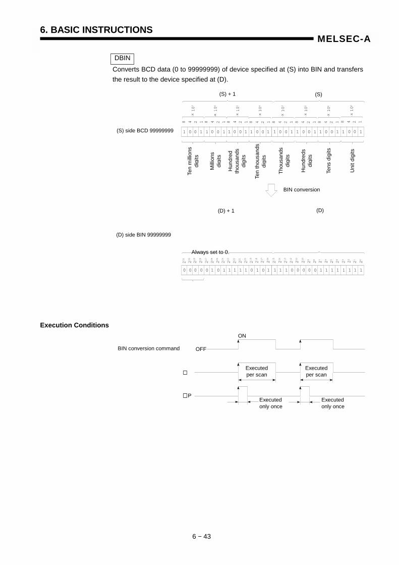
6. BASIC INSTRUCTIONS
6 − 43
MELSEC-A
DBIN Converts BCD data (0 to 99999999) of device specified at (S) into BIN and transfers the result to the device specified at (D).
Execution Conditions
0 00 01 1 10 0 1 11 10 10 11 1 0 0 00 0 1 11 11 1 11
230
229
224
221
223
225
226
227
228
220
222
231
219
210
211
212
213
214
215
216
217
218
26
29
20
2122
23
24
25
27
28
4 2107
x
18 4 2106
18 4 2105
18 4 2104
18 4 2103
18 4 2102
18 4 2101
18 4 2100
18
x x x x x x x
1 00 00 1 01 1 1 10 01 10 01 0 1 1 00 1 1 00 11 0 10
Always set to 0.
(S) side BCD 99999999
(D) side BIN 99999999
BIN conversion Te
n m
illion
s di
gits
(S) (S) + 1
Milli
ons
digi
ts
Hun
dred
th
ousa
nds
digi
ts
Ten
thou
sand
s di
gits
Thou
sand
s di
gits
Hun
dred
s di
gits
Tens
dig
its
Uni
t dig
its
(D) (D) + 1
OFF
ON
Executed per scan
Executed per scan
Executed only once
Executed only once
P
BIN conversion command
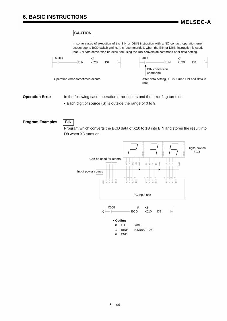
6. BASIC INSTRUCTIONS
6 − 44
MELSEC-A
CAUTION
In some cases of execution of the BIN or DBIN instruction with a NO contact, operation error occurs due to BCD switch timing. It is recommended, when the BIN or DBIN instruction is used, that BIN data conversion be executed using the BIN conversion command after data setting.
Operation Error In the following case, operation error occurs and the error flag turns on.
• Each digit of source (S) is outside the range of 0 to 9.
Program Examples BIN Program which converts the BCD data of X10 to 1B into BIN and stores the result into D8 when X8 turns on.
K4 BIN X020 D0
M9036 K4 BIN X020 D0
X000
BIN conversion command
After data setting, X0 is turned ON and data isread.
Operation error sometimes occurs.
800
400
200
100
80
40
20
10 8 4 2 1
COM
COM
COM
0 0 1 0 0 0 1 1 0 1 1 0
X1B
X1A
X19
X18
X1F
X1E
X1D
COM
X17
X16
X15
X14
X13
X12
X11
X10
X1C
PC input unit
Digital switch BCD
Can be used for others.
Input power source
•••• Coding 0 LD X008 1 BINP K3X010 D8 6 END
0 P K3 BCD X010 D8
X008
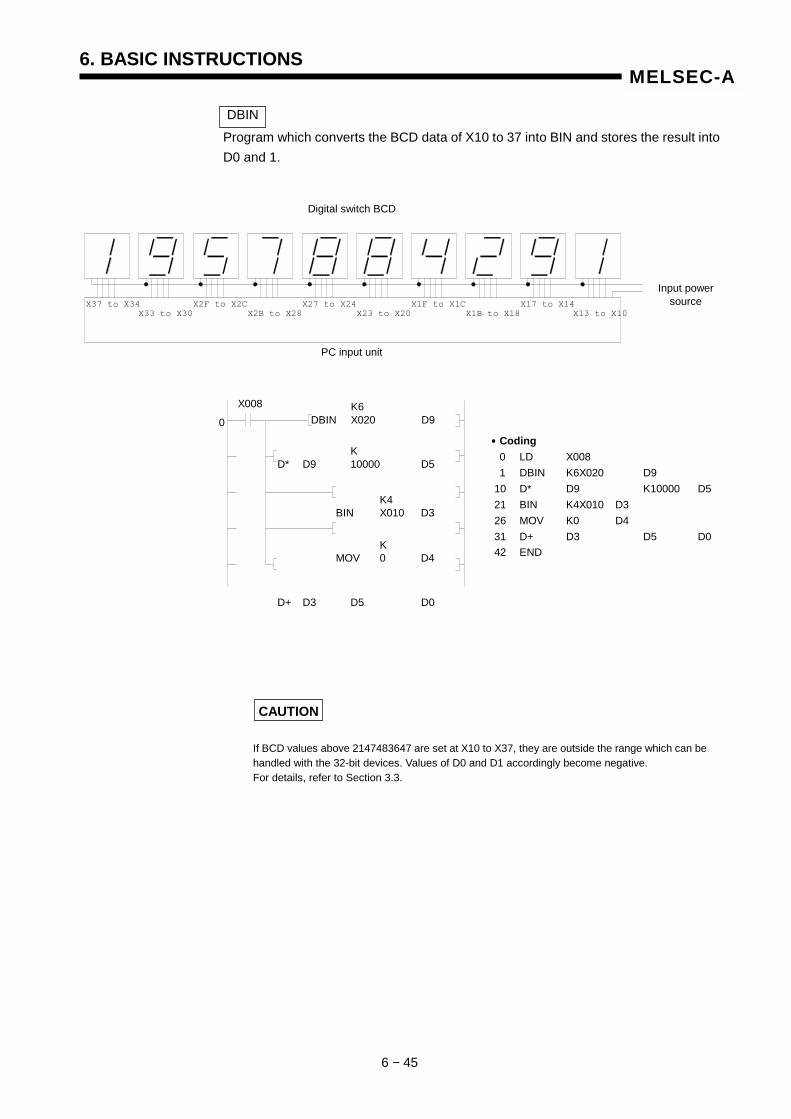
6. BASIC INSTRUCTIONS
6 − 45
MELSEC-A
DBIN Program which converts the BCD data of X10 to 37 into BIN and stores the result into D0 and 1.
CAUTION
If BCD values above 2147483647 are set at X10 to X37, they are outside the range which can be handled with the 32-bit devices. Values of D0 and D1 accordingly become negative. For details, refer to Section 3.3.
X37 to X34X33 to X30
X2F to X2CX2B to X28
X27 to X24X23 to X20
X1F to X1CX1B to X18
X17 to X14X13 to X10
PC input unit
Digital switch BCD
Input power source
•••• Coding 0 LD X008 1 DBIN K6X020 D9 10 D* D9 K10000 D5 21 BIN K4X010 D3 26 MOV K0 D4 31 D+ D3 D5 D0 42 END
0
K D* D9 10000 D5
X008 K6 DBIN X020 D9
K4 BIN X010 D3
K MOV 0 D4
D+ D3 D5 D0
6. BASIC INTRUCUTIONS
6 − 46
MELSEC-A
6.4 Data Transfer Instructions
The data transfer instructions are instructions which perform data transfer, interchanging data, the negative (reverse) data transfer, etc.
Classification Instruction Symbol Ref. Page
MOV 6-47
MOVP 6-47
DMOV 6-47 Transfer
DMOVP 6-47
CML 6-49
CMLP 6-49
DCML 6-49 Negative transfer
DCMLP 6-49
BMOV 6-52 Block transfer
BMOVP 6-52
FMOV 6-52 Same data
block transfer FMOVP 6-52
XCH 6-56
XCHP 6-56
DXCH 6-56 Interchange
DXCHP 6-56
POINT
The data moved by the data transfer instruction (transfer, interchanging, negative transfer, block transfer, block transfer of the same data) is retained until new data is transferred. Therefore, even if the execution command of each instruction turns off, the data does not change.
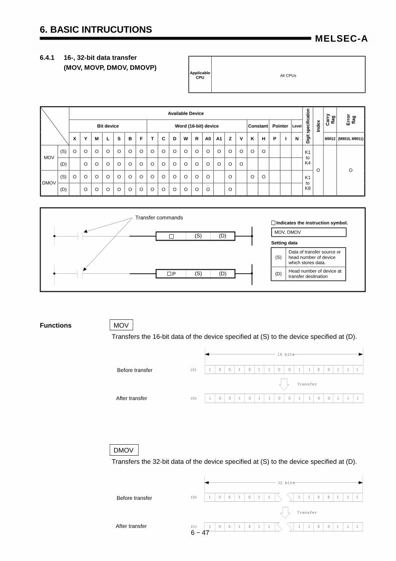
6. BASIC INTRUCUTIONS
6 − 47
MELSEC-A
6.4.1 16-, 32-bit data transfer (MOV, MOVP, DMOV, DMOVP)
Available Device
Bit device Word (16-bit) device Constant Pointer Level Car
ry
flag
Erro
r fla
g
X Y M L S B F T C D W R A0 A1 Z V K H P I N Digi
t spe
cific
atio
n
Inde
x
M9012 (M9010, M9011)
(S) O O O O O O O O O O O O O O O O O O MOV
(D) O O O O O O O O O O O O O O O
K1 to K4
(S) O O O O O O O O O O O O O O O O DMOV
(D) O O O O O O O O O O O O O
K1 to K8
O O
Functions MOV Transfers the 16-bit data of the device specified at (S) to the device specified at (D).
DMOV Transfers the 32-bit data of the device specified at (S) to the device specified at (D).
(S)
Transfer
1 0 0 1 11 0 0 0 1 1 10 0 11
(D) 1 0 0 1 11 0 0 0 1 1 10 0 11
16 bits
After transfer
Before transfer
(S) Data of transfer source or head number of device which stores data.
(D) Head number of device at transfer destination
MOV, DMOV
Indicates the instruction symbol.
Setting data
Transfer commands
(S) (D)
(S) (D) P
(S)
Transfer
(D)
32 bits
1 0 0 1 11 0 1 1 10 0 11
1 0 0 1 11 0 1 1 10 0 11
After transfer
Before transfer
Applicable CPU All CPUs
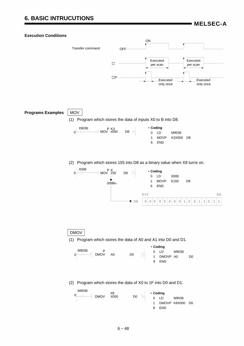
6. BASIC INTRUCUTIONS
6 − 48
MELSEC-A
Execution Conditions
Programs Examples MOV (1) Program which stores the data of inputs X0 to B into D8.
(2) Program which stores 155 into D8 as a binary value when X8 turns on.
DMOV
(1) Program which stores the data of A0 and A1 into D0 and D1.
(2) Program which stores the data of X0 to 1F into D0 and D1.
X9036 0 MOV x000 D8
P K3 • Coding 0 LD M9036 1 MOVP K3X000 D8 6 END
• Coding 0 LD M9036 1 DMOVP A0 D0 8 END
0 DMOV A0 D0 P M9036
0 DMOV X000 D0 X8
M9036 • Coding 0 LD M9036 1 DMOVP K8X000 D0 8 END
OFF
ON
Executed per scan
Executed per scan
Executed only once
Executed only once
P
Transfer command
X008 0 MOV 155 D8
P K • Coding 0 LD X008 1 MOVP K155 D8 6 END
009BH
b15
0000 11 00 00 00 11 10
b0
D8
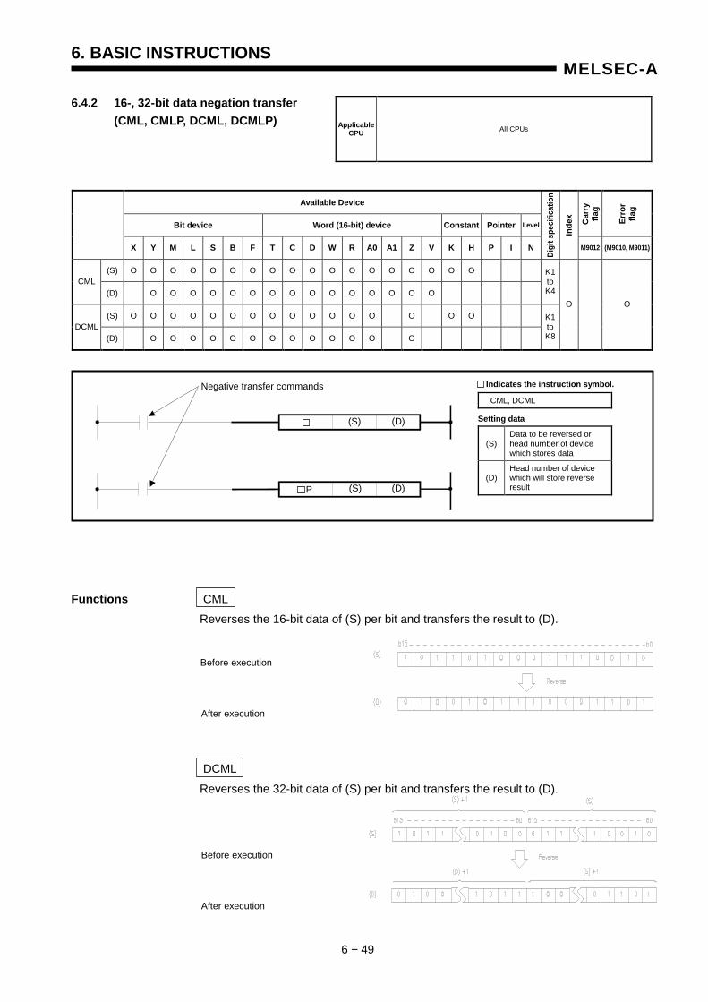
6. BASIC INSTRUCTIONS
6 − 49
MELSEC-A
6.4.2 16-, 32-bit data negation transfer (CML, CMLP, DCML, DCMLP)
Available Device
Bit device Word (16-bit) device Constant Pointer Level Car
ry
flag
Erro
r fla
g
X Y M L S B F T C D W R A0 A1 Z V K H P I N
Digi
t spe
cific
atio
n
Inde
x
M9012 (M9010, M9011)
(S) O O O O O O O O O O O O O O O O O O CML
(D) O O O O O O O O O O O O O O O
K1 to K4
(S) O O O O O O O O O O O O O O O O DCML
(D) O O O O O O O O O O O O O
K1 to K8
O O
Functions CML Reverses the 16-bit data of (S) per bit and transfers the result to (D).
DCML Reverses the 32-bit data of (S) per bit and transfers the result to (D).
Applicable CPU All CPUs
Before execution
After execution
Before execution
After execution
(S) Data to be reversed or head number of device which stores data
(D) Head number of device which will store reverse result
Setting data
CML, DCML
Indicates the instruction symbol.
(S) (D)
(S) (D)
Negative transfer commands
P
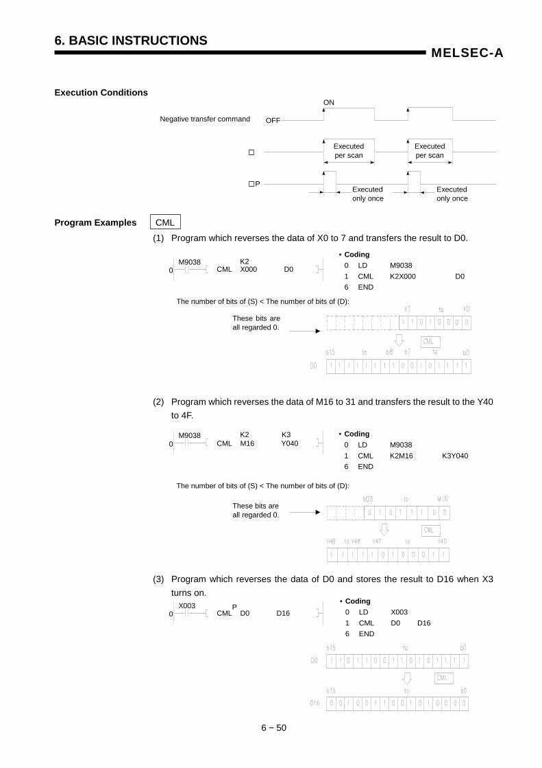
6. BASIC INSTRUCTIONS
6 − 50
MELSEC-A
Execution Conditions
Program Examples CML (1) Program which reverses the data of X0 to 7 and transfers the result to D0.
(2) Program which reverses the data of M16 to 31 and transfers the result to the Y40 to 4F.
(3) Program which reverses the data of D0 and stores the result to D16 when X3 turns on.
OFF
ON
Executed per scan
Executed per scan
Executed only once
Executed only once
P
Negative transfer command
0 X003
CML D0 D16 P
• Coding 0 LD X003 1 CML D0 D16 6 END
0
• Coding 0 LD M9038 1 CML K2X000 D0 6 END
M9038 CML X000 D0
K2
The number of bits of (S) < The number of bits of (D):
These bits areall regarded 0.
0 M9038
CML M16 Y040 K2 K3 • Coding
0 LD M9038 1 CML K2M16 K3Y040 6 END
The number of bits of (S) < The number of bits of (D):
These bits areall regarded 0.
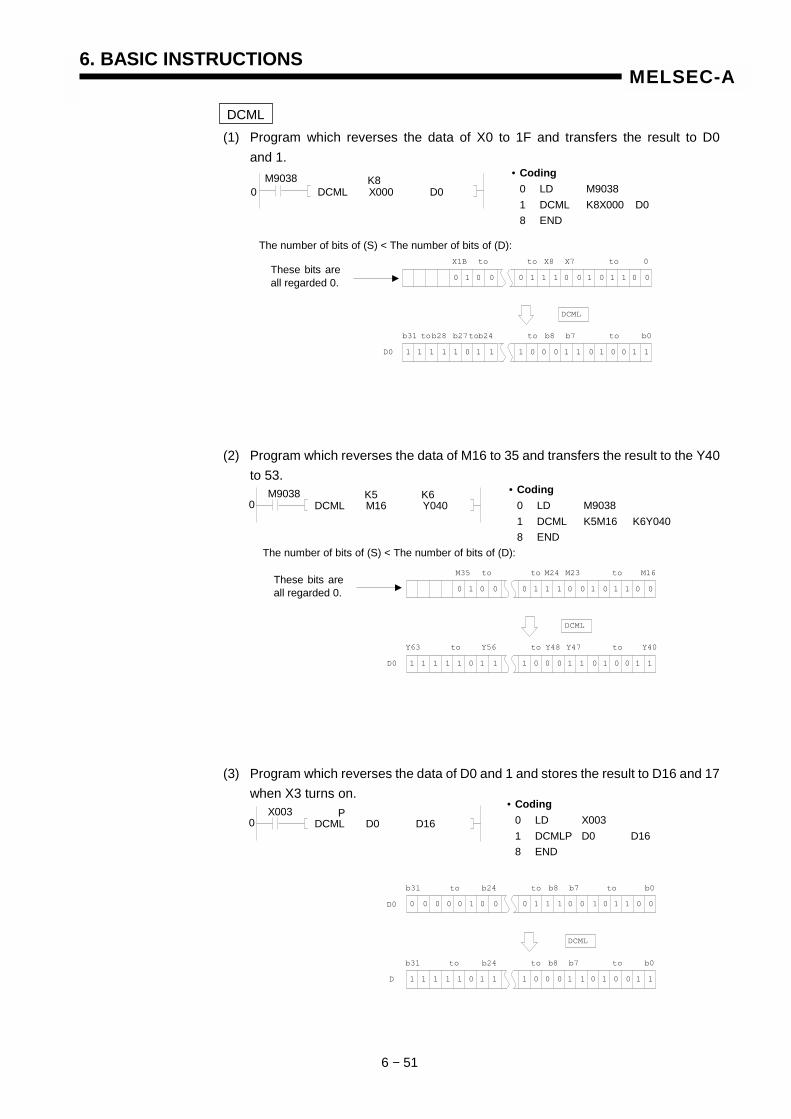
6. BASIC INSTRUCTIONS
6 − 51
MELSEC-A
DCML (1) Program which reverses the data of X0 to 1F and transfers the result to D0
and 1.
(2) Program which reverses the data of M16 to 35 and transfers the result to the Y40 to 53.
(3) Program which reverses the data of D0 and 1 and stores the result to D16 and 17 when X3 turns on.
0 0 11 10 1110 0 0 0 01 0
DCML
D0
X1B 0toX7X8toto
1 1 00 01 0001 1 1 1 10 1
b31 b0tob7b8toto
1 11 1
b28 b27 b24to
M9038 0 DCML X000 D0
K8 • Coding 0 LD M9038 1 DCML K8X000 D0 8 END
The number of bits of (S) < The number of bits of (D):
These bits are all regarded 0.
0 0 11 10 1110 0 0 0 01 0
DCML
D0
M35 M16toM23M24toto
1 1 00 01 0001 1 1 1 10 1
Y63 Y40toY47Y48toto
1 11 1
Y56
M9038 0 DCML M16 Y040
K5 K6 • Coding 0 LD M9038 1 DCML K5M16 K6Y040 8 END
The number of bits of (S) < The number of bits of (D):
These bits areall regarded 0.
X003 0 DCML D0 D16
P • Coding 0 LD X003 1 DCMLP D0 D16 8 END
0 0 11 10 1110 0 0 0 01 0
D
b31 b0tob7b8toto
1 1 00 01 0001 1 1 1 10 1
b31 b0tob7b8to
1 11 1
b24to
0 0 0 0
b24
DCML
D0

6. BASIC INSTRUCTIONS
6 − 51
MELSEC-A
DCML (1) Program which reverses the data of X0 to 1F and transfers the result to D0
and 1.
(2) Program which reverses the data of M16 to 35 and transfers the result to the Y40 to 53.
(3) Program which reverses the data of D0 and 1 and stores the result to D16 and 17 when X3 turns on.
M9038 0 DCML X000 D0
K8 • Coding 0 LD M9038 1 DCML K8X000 D0 8 END
The number of bits of (S) < The number of bits of (D):
These bits areall regarded 0.
M9038 0 DCML M16 Y040
K5 K6 • Coding 0 LD M9038 1 DCML K5M16 K6Y040 8 END
The number of bits of (S) < The number of bits of (D):
These bits areall regarded 0.
X003 0 DCML D0 D16
P • Coding 0 LD X003 1 DCMLP D0 D16 8 END
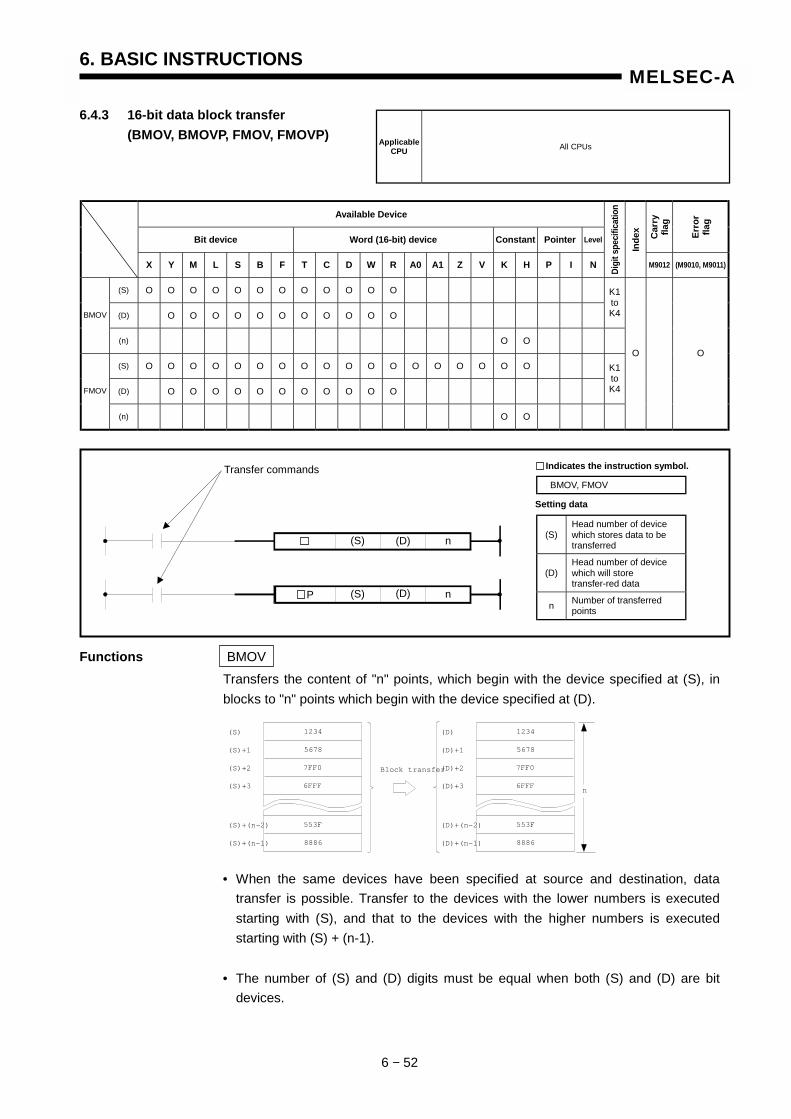
6. BASIC INSTRUCTIONS
6 − 52
MELSEC-A
6.4.3 16-bit data block transfer (BMOV, BMOVP, FMOV, FMOVP)
Available Device
Bit device Word (16-bit) device Constant Pointer Level Car
ry
flag
Erro
r fla
g
X Y M L S B F T C D W R A0 A1 Z V K H P I N Digi
t spe
cific
atio
n
Inde
x
M9012 (M9010, M9011)
(S) O O O O O O O O O O O O
(D) O O O O O O O O O O O
K1 to K4 BMOV
(n) O O
(S) O O O O O O O O O O O O O O O O O O
(D) O O O O O O O O O O O
K1 to K4 FMOV
(n) O O
O O
Functions BMOV Transfers the content of "n" points, which begin with the device specified at (S), in blocks to "n" points which begin with the device specified at (D).
• When the same devices have been specified at source and destination, data transfer is possible. Transfer to the devices with the lower numbers is executed starting with (S), and that to the devices with the higher numbers is executed starting with (S) + (n-1).
• The number of (S) and (D) digits must be equal when both (S) and (D) are bit
devices.
(S)+(n-1) 8886
(S)+(n-2) 553F
(S)+3 6FFF
(S)+2 7FF0
(S)+1 5678
(S) 1234
Block transfer
(D)+(n-1) 8886
(D)+(n-2) 553F
(D)+3 6FFF
(D)+2 7FF0
(D)+1 5678
(D) 1234
n
Applicable CPU All CPUs
Transfer commands
(S) (D) n
(S) (D) n P
(S) Head number of device which stores data to be transferred
(D) Head number of device which will store transfer-red data
n Number of transferred points
Setting data
BMOV, FMOV
Indicates the instruction symbol.
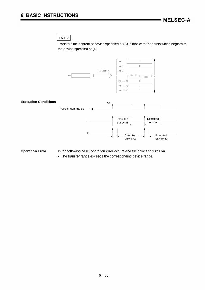
6. BASIC INSTRUCTIONS
6 − 53
MELSEC-A
FMOV Transfers the content of device specified at (S) in blocks to "n" points which begin with the device specified at (D).
Execution Conditions
Operation Error In the following case, operation error occurs and the error flag turns on. • The transfer range exceeds the corresponding device range.
(S)
Transfer
(D)+(n-1)
0(D)+(n-2)
0
(D)+2 0
(D)+1 0
(D) 0
n
0
(D)+(n-3)
OFF
ON
Transfer commands
Executed per scan
Executed per scan
Executed only once
Executed only once
P
OFF
ON
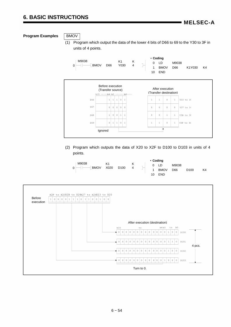
6. BASIC INSTRUCTIONS
6 − 54
MELSEC-A
Program Examples BMOV (1) Program which output the data of the lower 4 bits of D66 to 69 to the Y30 to 3F in
units of 4 points.
(2) Program which outputs the data of X20 to X2F to D100 to D103 in units of 4 points.
M9038 K1 K BMOV D66 Y030 4 0
• Coding 0 LD M9038 1 BMOV D66 K1Y030 K4 10 END
M9038 K1 K BMOV X020 D100 4 0
• Coding 0 LD M9038 1 BMOV D66 D100 K4 10 END
11 1 10
00 0 00
01 0 11
10 1 10
b15 .........b4 b3 b0............
D67
D66
D68
D69
1 1 0 1
0 0 0 0
0 0 1 1
1 1 0 1
Y33 to 30
Y37 to 34
Y3B to 38
Y3F to 3C
Before execution (Transfer source) After execution
(Transfer destination)
Ignored
1 0 0 1 10 0 1 0 1 1 10 0 00
X2F to X2CX2B to X28X27 to X24X23 to X20
b15 to b4b3 to b0
0 0 0 0 00 0 0 0 0 0 10 0 00
0 0 0 0 00 0 0 0 0 0 10 0 01
0 0 0 0 00 0 0 0 0 0 10 0 00
0 0 0 0 00 0 0 0 0 0 00 1 00
D101
D100
D102
D103
Turn to 0.
Before execution
After execution (destination)
4 pcs.

6. BASIC INSTRUCTIONS
6 − 55
MELSEC-A
FMOV (1) Program which outputs the data of the lower 4 bits of D0 to Y10 to 23 in units of 4
points when XA turn on.
(2) Program which outputs the data of X20 to X23 to D100 to D103 when XA is turned on.
• Coding 0 LD X00A 1 FMOVP D0 K1Y010 K5 10 END
0 P K1 K FMOV D0 Y010 5
X00A
• Coding 0 LD X00A 1 FMOVP K1X020 D100 K4 10 END
0 P K1 K FMOV X020 D100 4
X00A
1 0 1 1 11 0 1 0 0 1 10 1 01
X2F to X2CX2B to X28X27 to X24X23 to X20
b15 to b4b3 to b0
0 0 0 0 00 0 0 0 0 0 10 1 01
0 0 0 0 00 0 0 0 0 0 10 1 01
0 0 0 0 00 0 0 0 0 0 10 1 01
0 0 0 0 00 0 0 0 0 0 10 1 01
D101
D100
D102
D103
Before execution
Ignored.
After execution (destination)
Turn to 0.
4 pcs.
1 1 0 0 11 1 1 1 0 0 01 1 11
b4b15 b3 b2 b1 b0
1 0 1 1
1 0 1 1
1 0 1 1
1 0 1 1
1 0 1 1
Y13 to Y10
Y17 to Y14
Y1B to Y18
Y1F to Y1C
Y23 to Y20
................................................
D0
(S)
(D)
5 pc
s.
Ignored
Transfer
6. BASIC INSTRUCTIONS
6 − 56
MELSEC-A
6.4.4 16-, 32-bit data exchange (XCH, XCHP, DXCH, DXCHP)
Available Device
Bit device Word (16-bit) device Constant Pointer Level Car
ry
flag
Erro
r fla
g
X Y M L S B F T C D W R A0 A1 Z V K H P I N Digi
t spe
cific
atio
n
Inde
x
M9012 (M9010, M9011)
(D1) O O O O O O O O O O O O O O O XCH
(D2) O O O O O O O O O O O O O O O
K1 to K4
(D1) O O O O O O O O O O O O O DXCH
(D2) O O O O O O O O O O O O O
K1 to K8
O O
Functions XCH Interchanges the 16-bit data of (D1) and (D2).
DXCH Interchanges the 32-bit data of (D1) and (D2).
Applicable CPU All CPUs
1 0 0 1 010 11 00 0 10
16 bits 16 bits
(D1) (D2)
00 0 0 01 11 1 0 1 0 1 0
1 0 0 1 010 1 11 00 0 11 000 0 0 0 01 11 1 1 0 1 0 1 0
1 1 10Before execution
After execution
11 1 0 1 000 11 00 0 10 0 1 0 0 1 0 110 00 11 1 0 1 0
10 0 1 0 1100 11 1 0 1 0 1 1 0 1 0011 00 0 10 0 1
16 bits
(D1)
16 bits 16 bits 16 bits
(D1)+1 (D2)(D2)+2
0 0
Before execution
After execution
(D1)
(D2)
Head number of device which stores data to be interchanged
Setting data
XCH, DXCH
Indicates the instruction symbol. (D1) (D2)
(D1) (D2)
Interchange commands
P
6. BASIC INSTRUCTIONS
6 − 57
MELSEC-A
Execution Conditions
Program Examples XCH (1) Program which interchanges the present value of T0 and the content of D0 when
X8 turns on.
(2) Program which interchanges the content of D0 and the data of M16 to 31 when X10 turns on.
DXCH (1) Program which interchanges the content of D0 and 1 and the data of M16 to 47
when X10 turns on.
(2) Program which interchanges the content of D0 and 1 with that of D9 and 10 when M0 turns on.
0 X008 P
XCH T0 D0
• Coding 0 LD X008 1 XCHP T0 D0 6 END
0 X010 P K4
XCH D0 M16
• Coding 0 LD X010 1 XCHP D0 K4M16 6 END
• Coding 0 LD X010 1 DXCHP D0 K8M16 8 END
0 X010 P K8
DXCH D0 M16
• Coding 0 LD M0 1 DXCHP D0 D9 8 END
0 M0 P
DXCH D0 D9
OFF
ON
Interchange command
Executed per scan
Executed per scan
Executed only once
Executed only once
P
OFF
ON
6. BASIC INSTRUCTIONS
6 − 58
MELSEC-A
6.5 Program Branch Instructions
6.5.1 Conditional jump, unconditional jump (CJ, SCJ, JMP)
Available Device
Bit device Word (16-bit) device Constant Pointer Level Car
ry
flag
Erro
r fla
g
X Y M L S B F T C D W R A0 A1 Z V K H P I N Digi
t spe
cific
atio
n
Inde
x
M9012 (M9010, M9011)
P O O O
Functions CJ (1) Executes the program of specified pointer number when the jump command is
on. (2) Executes the program of the next step when the jump command is off.
Jump commands
Applicable CPU All CPUs
CJ P**
SCJ
JMP P**
P** Jump destination pointer number (Label)
P** * P255 indicates END and cannot be used as a label.
Jump command
CJ Executed per scan
P** Pointer number of jump destination (P0 to P255)
Setting data
ON
OFF
6. BASIC INSTRUCTIONS
6 − 59
MELSEC-A
SCJ (1) Executes the program of specified pointer number, starting at the next scan,
when the jump command changes from off to on. (2) Executes the program of the next step when the jump command is off or changes
from off to on.
JMP (1) Executes the program of specified pointer number unconditionally. Consider the following when the jump instructions are used. (2) Even if the timer, of which coil is on, is jumped by the CJ, SCJ, or JMP instruction
after the coil of timer is turned on, the timer continues counting. (3) If the OUT instruction is jumped by CJ, SCJ or JMP, coil status is held
unchanged. (4) When a jump is made to a memory location by CJ, SCJ, or JMP, the scan timer is
shortened. (5) The CJ, SCJ, and JMP instructions are also capable of jumping to a step with
lower number. However, it is necessary to exit this closed loop before the watch dog timer times out.
Jump command
SCJ 1 scan Executed per scan
( )
( )
Closed loopwhen X3 isON.
P8 X000
X007
X003
X006 P9
CJ P9
CJ P8
Y040
Y042
Exits the loop when X7 isturned ON.
ON
OFF

6. BASIC INSTRUCTIONS
6 − 60
MELSEC-A
(6) The device jumped by CJ, SCJ, or JMP does not change.
(7) The label (P**) occupies one step.
( )
( )
( )
When XB turn on, jump is made to the label P19.
Even if XB and C turn on/off during the execution ofCJ instruction, Y43 and 49 do not change.
10
14
16
18
X00B
X00C
X00B
X009 P19
CJ P19
Y043
Y049
Y04C
( )
( )
( )
( )
10
14
16
18
21
P9
X008
M33
M3
M36
X009
Occupies one step.
CJ P9
Y030
Y036
Y039
Y03B
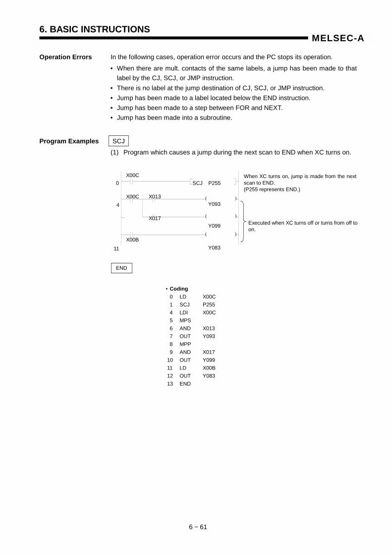
6. BASIC INSTRUCTIONS
6 − 61
MELSEC-A
Operation Errors In the following cases, operation error occurs and the PC stops its operation.
• When there are mult. contacts of the same labels, a jump has been made to that label by the CJ, SCJ, or JMP instruction.
• There is no label at the jump destination of CJ, SCJ, or JMP instruction. • Jump has been made to a label located below the END instruction. • Jump has been made to a step between FOR and NEXT. • Jump has been made into a subroutine.
Program Examples SCJ (1) Program which causes a jump during the next scan to END when XC turns on.
( )
( )
( )
0
4
11
X00C
X00C
X00B
X013
X017
SCJ P255
Y093
Y099
Y083
When XC turns on, jump is made from the nextscan to END. (P255 represents END.)
Executed when XC turns off or turns from off to on.
END
• Coding 0 LD X00C 1 SCJ P255 4 LDI X00C 5 MPS 6 AND X013 7 OUT Y093 8 MPP 9 AND X017 10 OUT Y099 11 LD X00B 12 OUT Y083 13 END
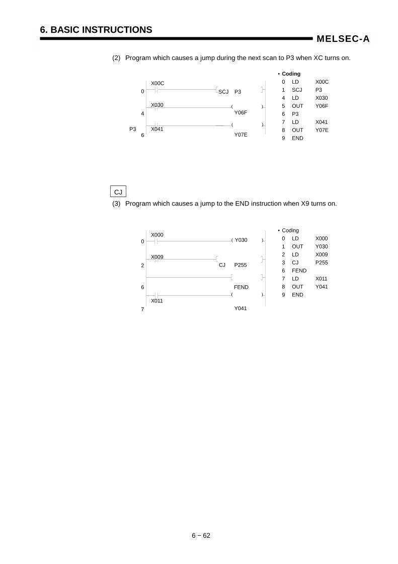
6. BASIC INSTRUCTIONS
6 − 62
MELSEC-A
(2) Program which causes a jump during the next scan to P3 when XC turns on.
CJ (3) Program which causes a jump to the END instruction when X9 turns on.
( )
( )
0
4
6 P3
X00C
X030
X041
SCJ P3
Y06F
Y07E
• Coding 0 LD X00C 1 SCJ P3 4 LD X030 5 OUT Y06F 6 P3 7 LD X041 8 OUT Y07E 9 END
( )
( )
0
2 X009
6
7
CJ P255
X000
X011
Y030
FEND
Y041
• Coding 0 LD X000 1 OUT Y030 2 LD X009 3 CJ P255 6 FEND 7 LD X011 8 OUT Y041 9 END
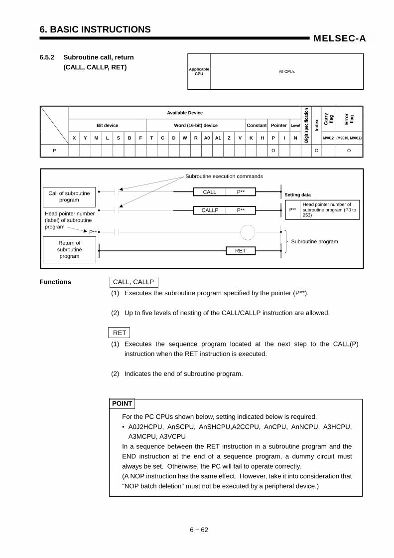
6. BASIC INSTRUCTIONS
6 − 62
MELSEC-A
6.5.2 Subroutine call, return (CALL, CALLP, RET)
Available Device
Bit device Word (16-bit) device Constant Pointer Level Car
ry
flag
Erro
r fla
g
X Y M L S B F T C D W R A0 A1 Z V K H P I N Digi
t spe
cific
atio
n
Inde
x
M9012 (M9010, M9011)
P O O O
Functions CALL, CALLP (1) Executes the subroutine program specified by the pointer (P**). (2) Up to five levels of nesting of the CALL/CALLP instruction are allowed.
RET (1) Executes the sequence program located at the next step to the CALL(P)
instruction when the RET instruction is executed. (2) Indicates the end of subroutine program.
POINT
For the PC CPUs shown below, setting indicated below is required. • A0J2HCPU, AnSCPU, AnSHCPU,A2CCPU, AnCPU, AnNCPU, A3HCPU, A3MCPU, A3VCPU In a sequence between the RET instruction in a subroutine program and the END instruction at the end of a sequence program, a dummy circuit must always be set. Otherwise, the PC will fail to operate correctly. (A NOP instruction has the same effect. However, take it into consideration that "NOP batch deletion" must not be executed by a peripheral device.)
Applicable CPU All CPUs
Subroutine execution commands
P**
RET
CALL
P** Head pointer number of subroutine program (P0 to 253)
Setting data
Subroutine program
P** CALLP
Call of subroutine program
Head pointer number (label) of subroutine program
Return of subroutine program
P**
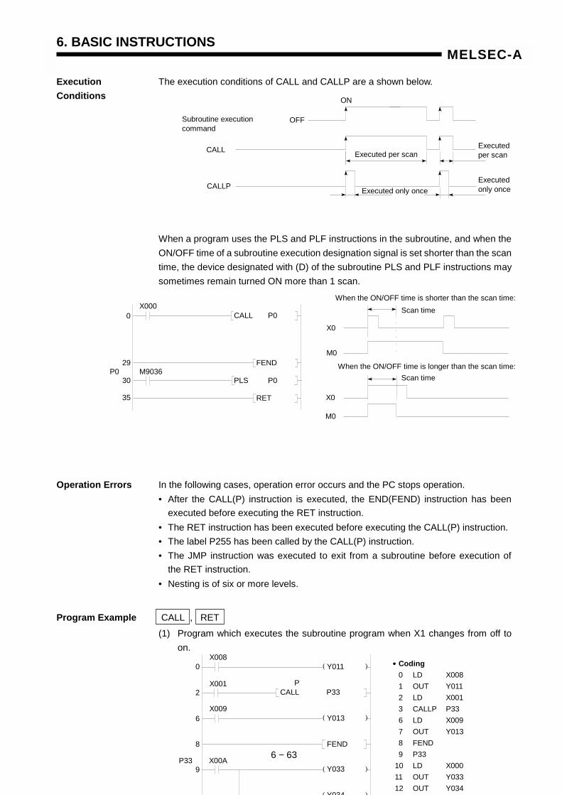
6. BASIC INSTRUCTIONS
6 − 63
MELSEC-A
Execution The execution conditions of CALL and CALLP are a shown below. Conditions
When a program uses the PLS and PLF instructions in the subroutine, and when the ON/OFF time of a subroutine execution designation signal is set shorter than the scan time, the device designated with (D) of the subroutine PLS and PLF instructions may sometimes remain turned ON more than 1 scan.
Operation Errors In the following cases, operation error occurs and the PC stops operation. • After the CALL(P) instruction is executed, the END(FEND) instruction has been executed before executing the RET instruction. • The RET instruction has been executed before executing the CALL(P) instruction. • The label P255 has been called by the CALL(P) instruction. • The JMP instruction was executed to exit from a subroutine before execution of the RET instruction. • Nesting is of six or more levels.
Program Example CALL , RET (1) Program which executes the subroutine program when X1 changes from off to
on.
OFF
ON
Executed per scan Executed per scan
Executed only once Executed only once
CALL
CALLP
Subroutine execution command
( )
( )
( )
( )
P CALL P33
Y011 X008
0
2
6
P33
8
9
X001
X009
X00A
Y013
FEND
Y033
Y034
•••• Coding 0 LD X008 1 OUT Y011 2 LD X001 3 CALLP P33 6 LD X009 7 OUT Y013 8 FEND 9 P33 10 LD X000 11 OUT Y033 12 OUT Y034
When the ON/OFF time is shorter than the scan time:
When the ON/OFF time is longer than the scan time:
X0
M0
X0
M0
Scan time
Scan time
CALL P0
FEND
X000
M9036 PLS P0
RET
29
30
35
P0
0

6. BASIC INSTRUCTIONS
6 − 64
MELSEC-A
6.5.3 Interrupt enable, disable, return (EI, DI, IRET)
The EI and DI instructions used with the AnN, AnS, AnSH, A1FX, A0J2H and A73 vary in function with status of special relay M9053, as mentioned below. When M9053 is ON: Link refresh enable/disable (See Section 6.7.2 for details.) When M9053 is OFF: Interrupt enable/disable
Available Device
Bit device Word (16-bit) device Constant Pointer Level Car
ry
flag
Erro
r fla
g
X Y M L S B F T C D W R A0 A1 Z V K H P I N Digi
t spe
cific
atio
n
Inde
x
M9012 (M9010, M9011)
Functions DI (1) Disables the interrupt program until the EI instruction is executed so that interrupt
signals are ignored. (2) When the PC CPU is RESET, interrupt program execution is disabled.
EI (1) Enables the interrupt program.
AnS AnN
AnSH An A1FX A3H
A3M A3V AnA AnU A2AS A0J2H A2C
A52G A73 A3N board Applicable
CPU O O X O O X
Remark * EI and DI instructions are valid only when special relay M9053 is OFF.
EI Program execution continues
IRET Interrupt program
Required to the AnN, AnS,AnSH, A1FX, A0J2H, A73and A3N board
Interrupt pointer (10 to 31) (Label)
M9036 RST M9053
RST M9053
DI
EI
IRET
M9036
I**
Sequence program
Sequence program
Interrupt program
DI
EI
FEND In
Any interrupt signal occuring between DI and EI instructions, is disabled untilthe processing between the DI and EI instructions is completed after which the interrupt program is run.
* * * * *
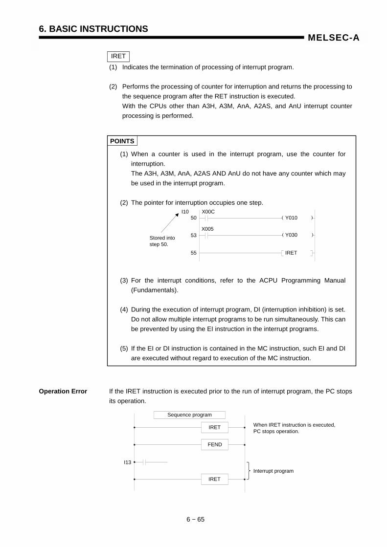
6. BASIC INSTRUCTIONS
6 − 65
MELSEC-A
IRET (1) Indicates the termination of processing of interrupt program. (2) Performs the processing of counter for interruption and returns the processing to
the sequence program after the RET instruction is executed. With the CPUs other than A3H, A3M, AnA, A2AS, and AnU interrupt counter
processing is performed.
POINTS
(1) When a counter is used in the interrupt program, use the counter for interruption.
The A3H, A3M, AnA, A2AS AND AnU do not have any counter which may be used in the interrupt program.
(2) The pointer for interruption occupies one step. (3) For the interrupt conditions, refer to the ACPU Programming Manual
(Fundamentals). (4) During the execution of interrupt program, DI (interruption inhibition) is set.
Do not allow multiple interrupt programs to be run simultaneously. This can be prevented by using the EI instruction in the interrupt programs.
(5) If the EI or DI instruction is contained in the MC instruction, such EI and DI
are executed without regard to execution of the MC instruction.
Operation Error If the IRET instruction is executed prior to the run of interrupt program, the PC stops its operation.
( )
( )I10
50 X00C
X005
Y010
Y030
IRET
53
55
Stored into step 50.
Sequence program
IRET
FEND
IRET
I13
When IRET instruction is executed, PC stops operation.
Interrupt program
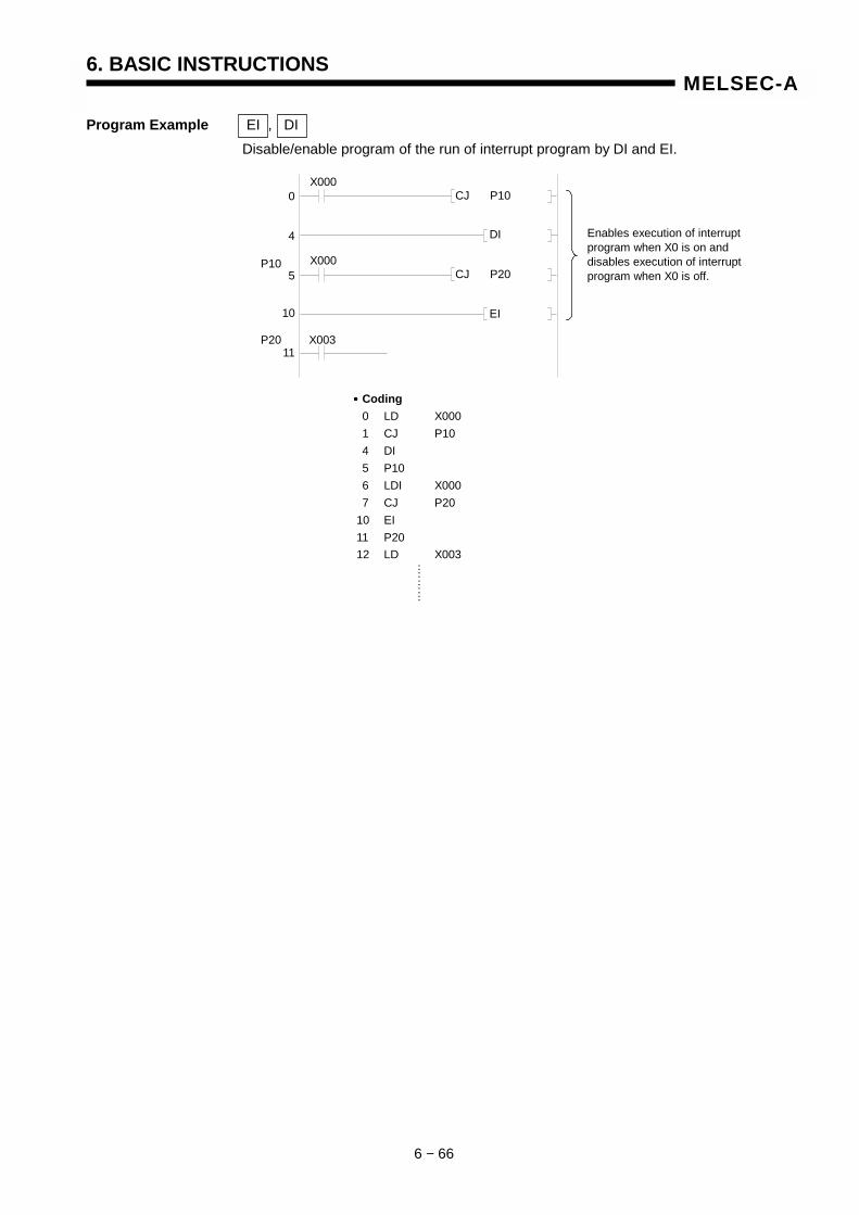
6. BASIC INSTRUCTIONS
6 − 66
MELSEC-A
Program Example EI , DI Disable/enable program of the run of interrupt program by DI and EI.
CJ P20
X000 0
4
5
10
X000
X003
DI
EI
11
CJ P10
Enables execution of interrupt program when X0 is on and disables execution of interrupt program when X0 is off.
P20
P10
•••• Coding 0 LD X000 1 CJ P10 4 DI 5 P10 6 LDI X000 7 CJ P20 10 EI 11 P20 12 LD X003
……
….

6. BASIC INSTRUCTIONS
6 − 67
MELSEC-A
6.5.4 Microcomputer program call (SUB, SUBP)
The SUB instruction of the AnA, A2AS and AnU becomes the 16-bit constant setting instruction in the extension application instructions. For details, refer to the AnSHCPU/AnACPU/AnUCPU Programming Manual (Dedicated Instructions).
Available Device
Bit device Word (16-bit) device Constant Pointer Level Car
ry
flag
Erro
r fla
g
X Y M L S B F T C D W R A0 A1 Z V K H P I N
Digi
t spe
cific
atio
n
Inde
x
M9012 (M9010, M9011)
n O O O O O O O O O O O O O
Functions (1) Calls the microcomputer program created by user and allows the run of microcomputer program.
(2) When the run of microcomputer program is completed, runs the sequence
program again, starting at the next step to the SUB or SUBP instruction. (3) The SUB and SUBP instructions can be used for the sequence program and
subsequence program.
AnSAnN
AnSHAn A1FX A3H
A3M A3V AnA AnU A2AS A0J2H A2C
A52G A73 A3NboardApplicable
CPU O O O O O X X O O O O
Remark
n Head address of micro-computer program
Setting data
Microcomputer program execution commands
n SUB
n SUBP
Parameter Set value of
timer/counter
SUB(P)
END Microcomputer
program RET
Sequence program area
Microcomputer program area
Main (sub) program area

6. BASIC INSTRUCTIONS
6 − 68
MELSEC-A
(4) In the microcomputer program area, multiple microcomputer programs can be
created.
(5) For the details of microcomputer program, see Section 8.
Execution The execution conditions of SUB and SUBP instructions are as shown below. Conditions
Operation Error In the following case, operation error occurs and the error flag turns on. • An area of more than the microcomputer program capacity has been specified at n.
POINTS
(1) The processing time of a microcomputer program called by one SUB instruction must be 5 msec or less. If it exceeds 5 msec, operation combination between the microcomputer program processing and the internal processing of the PC becomes out of control and the PC cannot run correctly.
(2) If a microcomputer program which needs more than 5 msec for processing is to be executed, divide it into several blocks which are called consecutively. This method can shorten the processing time of a microcomputer program called by one SUB instruction.
H SUB 0930
X010
X011
H SUB 0500
500H Microcomputer program
930H Microcomputer program
0
Head of microcomputerprogram
OFF ON
Executed per scan
Executed per scan
Executed only once
Executed only once
SUB
SUBP
Microcomputer program execution command
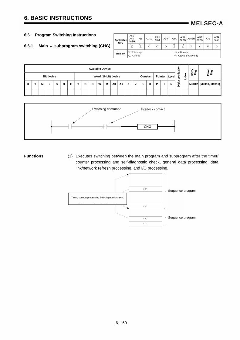
6. BASIC INSTRUCTIONS
6 − 69
MELSEC-A
6.6 Program Switching Instructions
6.6.1 Main ↔↔↔↔ subprogram switching (CHG)
Available Device
Bit device Word (16-bit) device Constant Pointer Level Car
ry
flag
Erro
r fla
g
X Y M L S B F T C D W R A0 A1 Z V K H P I N Digi
t spe
cific
atio
n
Inde
x
M9012 (M9010, M9011)
Functions (1) Executes switching between the main program and subprogram after the timer/ counter processing and self-diagnostic check, general data processing, data link/network refresh processing, and I/O processing.
AnS AnN
AnSH An A1FX A3H
A3M A3V AnA AnU A2AS A0J2H A2C
A52G A73 A3N boad Applicable
CPU X O O X X O O
Remark *1: A3N only *3: A3A only *2: A3 only *4: A3U and A4U only
Switching command Interlock contact
CHG
*1 *2 *3 *4
CHG
END
CHG
Sequence program
END
Sequence program
Timer, counter processing Self-diagnostic check,
l d t i d t li k/ t k
Sequence program
Sequence program
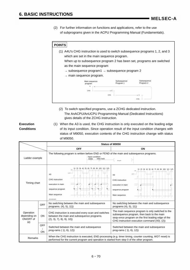
6. BASIC INSTRUCTIONS
6 − 70
MELSEC-A
(2) For further information on functions and applications, refer to the use of subprograms given in the ACPU Programming Manual (Fundamentals).
POINTS
(1) A4U's CHG instruction is used to switch subsequence programs 1, 2, and 3 which are set in the main sequence program.
When up to subsequence program 2 has been set, programs are switched as the main sequence program
→ subsequence program1 → subsequence program 2 → main sequence program.
(2) To switch specified programs, use a ZCHG dedicated instruction. The AnACPU/AnUCPU Programming Manual (Dedicated Instructions)
Execution (1) When the A3 is used, the CHG instruction is only executed on the leading edge Conditions of its input condition. Since operation result of the input condition changes with status of M9050, execution contents of the CHG instruction change with status of M9050.
Status of M9050
OFF ON
Ladder example
The following program is written before END or FEND of the main and subsequence programs.
Timing chart
OFF No switching between the main and subsequence programs. (4), 5), 11))
No switching between the main and subsequence programs (4), 5), 11))
ON CHG instruction is executed every scan and switches between the main and subsequence programs. (2), 3), 7), 8), 9), 10))
The main sequence program is only switched to the subsequence program, then back to the main sequ-ence program on the first leading edge of the CHG instruction execution command (X0). (2))
Operation depending on
ON/OFF of X0
OFF ↓
ON
Switched between the main and subsequence prog-rams ( 1), 6), 12))
Switched between the main and subsequence prog-rams ( 1), 6), 12))
Remarks When the CHG instruction is executed, END processing (e.g. timer timing, counter counting, WDT reset) is performed for the current program and operation is started from step 0 of the other program.
X0
CHG instruction
execution in main
sequence program
Main sequence
program
OFF
ON1) 2) 3) 4) 5) 6) 7) 8) 9) 10) 11) 12)
X0
CHG instruction
execution in main
sequence program
Main sequence
program
OFF
ON1) 2) 3) 4) 5) 6) 7) 8) 9) 10) 11) 12)
X000 Inter lock CHG
Input condition
Main sequence program
Subsequence Program 1
Subsequence Program 2
CHG
CHG
CHG
0
0
0
gives details of the ZCHG instruction.
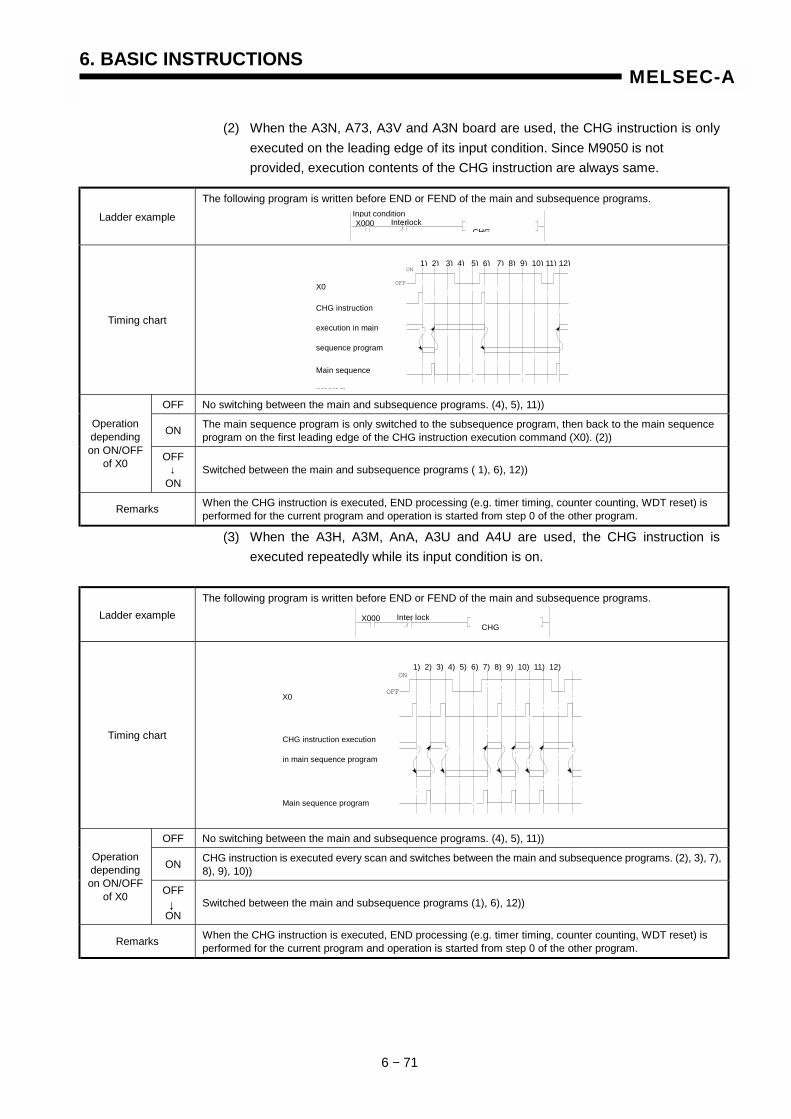
6. BASIC INSTRUCTIONS
6 − 71
MELSEC-A
(2) When the A3N, A73, A3V and A3N board are used, the CHG instruction is only executed on the leading edge of its input condition. Since M9050 is not
provided, execution contents of the CHG instruction are always same.
Ladder example
The following program is written before END or FEND of the main and subsequence programs.
Timing chart
OFF No switching between the main and subsequence programs. (4), 5), 11))
ON The main sequence program is only switched to the subsequence program, then back to the main sequence program on the first leading edge of the CHG instruction execution command (X0). (2))
Operation depending on ON/OFF
of X0 OFF ↓
ON Switched between the main and subsequence programs ( 1), 6), 12))
Remarks When the CHG instruction is executed, END processing (e.g. timer timing, counter counting, WDT reset) is performed for the current program and operation is started from step 0 of the other program.
(3) When the A3H, A3M, AnA, A3U and A4U are used, the CHG instruction is executed repeatedly while its input condition is on.
Ladder example The following program is written before END or FEND of the main and subsequence programs.
Timing chart
OFF No switching between the main and subsequence programs. (4), 5), 11))
ON CHG instruction is executed every scan and switches between the main and subsequence programs. (2), 3), 7), 8), 9), 10))
Operation depending on ON/OFF
of X0 OFF
ON Switched between the main and subsequence programs (1), 6), 12))
Remarks When the CHG instruction is executed, END processing (e.g. timer timing, counter counting, WDT reset) is performed for the current program and operation is started from step 0 of the other program.
X000 Interlock CHG
Input condition
X0
CHG instruction execution
in main sequence program
Main sequence program
OFF
ON1) 2) 3) 4) 5) 6) 7) 8) 9) 10) 11) 12)
X000 Inter lock CHG
↓
X0
CHG instruction
execution in main
sequence program
Main sequence
program
OFF
ON1) 2) 3) 4) 5) 6) 7) 8) 9) 10) 11) 12)

6. BASIC INSTRUCTIONS
6 − 72
MELSEC-A
Execution of PLS Instruction Used with CHG Instruction
(1) When the A3 is used, execution contents of the PLS instruction change with status of M9050 when other input conditions are same.
Status of M9050
OFF ON
Ladder example
The following program is written at step 0 of the main and subsequence programs.
Timing chart
OFF M0 is not switched on. M0 is not switched on.
ON M0 is only switched on during the first scan after switched by the CHG instruction.
M0 is only switched on during the first scan of the subsequence program selected by the CHG instruction executed after X0 is switched on.
Ope
ratio
n
X0 status
OFF ↓
ON M0 is only switched on during 1 scan. M0 is only switched on during 1 scan.
(2) When the A3N, A73 and A3V are used, execution contents are always same.
Ladder example
The following program is written at step 0 of the main and subsequence programs.
Timing chart
OFF M0 is not switched on.
ON M0 is only switched on during the first scan of the subsequence program selected by the CHG instruction executed after X0 is switched on.
Ope
ratio
n
X0 status OFF
↓ ON
M0 is only switched on during 1 scan.
X000 PLS M0
Input condition
Main sequence
program run
Subsequence
program run
OFF
ON
OFF
ON
CHG instruction execution
CHG instruction execution1 scan
Main sequence
program run
Subsequence
program run
OFF
ON
OFF
ON
CHG instruction execution
CHG instruction execution
1scan
CHG instruction execution
OFF
ON
OFF
ON
Main sequence
program run
Subsequence
program run
1 scan
CHG instruction execution
X000 PLS M0
Input condition
0
0

6. BASIC INSTRUCTIONS
6 − 73
MELSEC-A
(3) When the A3H, A3M, A3A, A3U and A4U are used, the CHG instruction is executed repeatedly while its input condition is on.
Ladder example
The following program is written before END or FEND of the main and subsequence programs.
Timing chart
OFF M0 is not switched on.
ON M0 is only switched on during the first scan of the subsequence program selected by the CHG instruction executed after X0 is switched on.
Ope
ratio
n
X0 status OFF
↓ ON
M0 is only switched on during 1 scan.
X000 PLS M0
Input condition
Main sequence
program run
Subsequence
program run
OFF
ON
OFF
ON
CHG instruction execution
CHG instruction execution
1 scan
0
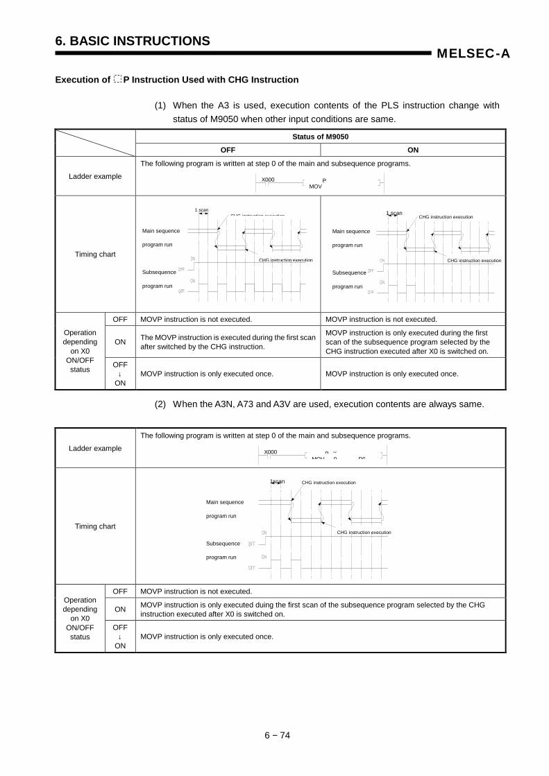
6. BASIC INSTRUCTIONS
6 − 74
MELSEC-A
Execution of P Instruction Used with CHG Instruction
(1) When the A3 is used, execution contents of the PLS instruction change with status of M9050 when other input conditions are same.
Status of M9050
OFF ON
Ladder example
The following program is written at step 0 of the main and subsequence programs.
Timing chart
OFF MOVP instruction is not executed. MOVP instruction is not executed.
ON The MOVP instruction is executed during the first scan after switched by the CHG instruction.
MOVP instruction is only executed during the first scan of the subsequence program selected by the CHG instruction executed after X0 is switched on.
Operation depending
on X0 ON/OFF status OFF
↓ ON
MOVP instruction is only executed once. MOVP instruction is only executed once.
(2) When the A3N, A73 and A3V are used, execution contents are always same.
Ladder example
The following program is written at step 0 of the main and subsequence programs.
Timing chart
OFF MOVP instruction is not executed.
ON MOVP instruction is only executed duing the first scan of the subsequence program selected by the CHG instruction executed after X0 is switched on.
Operation depending
on X0 ON/OFF status
OFF ↓
ON MOVP instruction is only executed once.
CHG instruction execution1 scan
Main sequence
program run
Subsequence
program run
CHG instruction execution
CHG instruction execution1 scan
Main sequence
program run
Subsequence
program run
CHG instruction execution
CHG instruction execution 1scan
Main sequence
program run
Subsequence
program run
CHG instruction execution
MOV PX000
X000 MOV 0 D0
P K
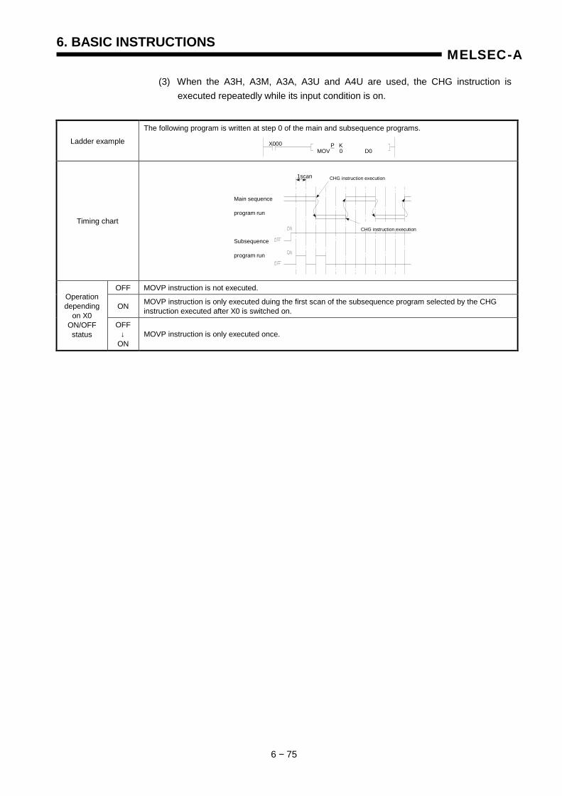
6. BASIC INSTRUCTIONS
6 − 75
MELSEC-A
(3) When the A3H, A3M, A3A, A3U and A4U are used, the CHG instruction is executed repeatedly while its input condition is on.
Ladder example
The following program is written at step 0 of the main and subsequence programs.
Timing chart
OFF MOVP instruction is not executed.
ON MOVP instruction is only executed duing the first scan of the subsequence program selected by the CHG instruction executed after X0 is switched on.
Operation depending
on X0 ON/OFF status
OFF ↓
ON MOVP instruction is only executed once.
CHG instruction execution 1scan
Main sequence
program run
Subsequence
program run
CHG instruction execution
X000 MOV 0 D0
P K
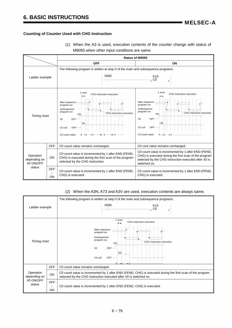
6. BASIC INSTRUCTIONS
6 − 76
MELSEC-A
Counting of Counter Used with CHG Instruction
(1) When the A3 is used, execution contents of the counter change with status of M9050 when other input conditions are same.
Status of M9050
OFF ON
Ladder example
The following program is written at step 0 of the main and subsequence programs.
Timing chart
OFF C0 count value remains unchanged. C0 cont value remains unchanged.
ON C0 count value is incremented by 1 after END (FEND, CHG) is executed during the first scan of the program selected by the CHG instruction.
C0 count value is incremented by 1 after END (FEND, CHG) is executed during the first scan of the program selected by the CHG instruction executed after X0 is switched on.
Operation depending on X0 ON/OFF
status OFF ↓
ON
C0 count value is incremented by 1 after END (FEND, CHG) is executed.
C0 count value is incremented by 1 after END (FEND, CHG) is executed.
(2) When the A3N, A73 and A3V are used, execution contents are always same.
Ladder example
The following program is written at step 0 of the main and subsequence programs.
Timing chart
OFF C0 count value remains unchanged.
ON C0 count value is incremented by 1 after END (FEND, CHG) is executed during the first scan of the program selected by the CHG instruction executed after X0 is switched on.
Operation depending on X0 ON/OFF
status OFF ↓
ON C0 count value is incremented by 1 after END (FEND, CHG) is executed.
( )
X000 K10C0
1 scan
Main sequence program run
CHG instruction execution
Subsequence program run
X0 OFF
ON
C0 coil OFF
ON
C0 count value 1 2 0 3 4
CHG instruction execution
1 scan
Main sequence program run
CHG instruction execution
Subsequence program run
X0 OFF
ON
C0 coil OFF
ON
C0 count value 1 2 0
CHG instruction execution
( )
X000 K10C0
1 scanCHG instruction execution
Main sequenceprogram run
Subsequence program run
CHG instruction execution
X0 OFF
ON
C0 coil OFF
0 1
ON
2
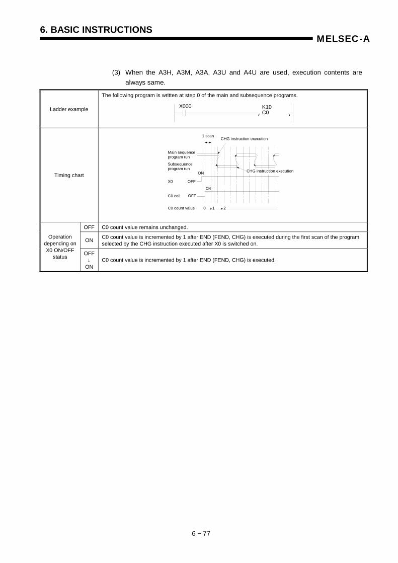
6. BASIC INSTRUCTIONS
6 − 77
MELSEC-A
(3) When the A3H, A3M, A3A, A3U and A4U are used, execution contents are always same.
Ladder example
The following program is written at step 0 of the main and subsequence programs.
Timing chart
OFF C0 count value remains unchanged.
ON C0 count value is incremented by 1 after END (FEND, CHG) is executed during the first scan of the program selected by the CHG instruction executed after X0 is switched on.
Operation depending on X0 ON/OFF
status OFF ↓
ON C0 count value is incremented by 1 after END (FEND, CHG) is executed.
( )
X000 K10C0
1 scan
Main sequenceprogram run
CHG instruction execution
Subsequence program run
X0 OFF
ON
C0 coil OFF
ON
C0 count value 1 20
CHG instruction execution
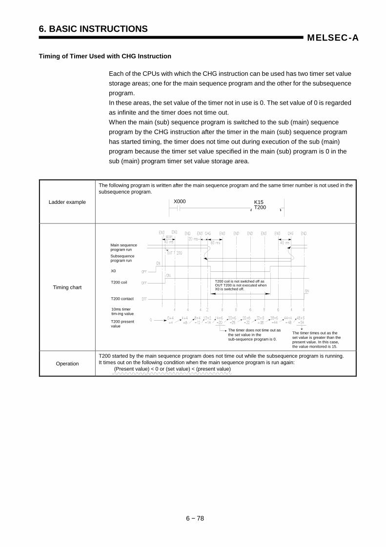
6. BASIC INSTRUCTIONS
6 − 78
MELSEC-A
Timing of Timer Used with CHG Instruction
Each of the CPUs with which the CHG instruction can be used has two timer set value storage areas; one for the main sequence program and the other for the subsequence program. In these areas, the set value of the timer not in use is 0. The set value of 0 is regarded as infinite and the timer does not time out. When the main (sub) sequence program is switched to the sub (main) sequence program by the CHG instruction after the timer in the main (sub) sequence program has started timing, the timer does not time out during execution of the sub (main) program because the timer set value specified in the main (sub) program is 0 in the sub (main) program timer set value storage area.
Ladder example
The following program is written after the main sequence program and the same timer number is not used in the subsequence program.
Timing chart
Operation T200 started by the main sequence program does not time out while the subsequence program is running. It times out on the following condition when the main sequence program is run again: (Present value) < 0 or (set value) < (present value)
( )
X000 K15T200
Main sequence program run Subsequence program run
X0
T200 coil
The timer does not time out as the set value in the sub-sequence program is 0.
The timer times out as the set value is greater than the present value. In this case, the value monitored is 15.
T200 contact
T200 coil is not switched off as OUT T200 is not executed whenX0 is switched off.
10ms timer tim-ing value
T200 present value
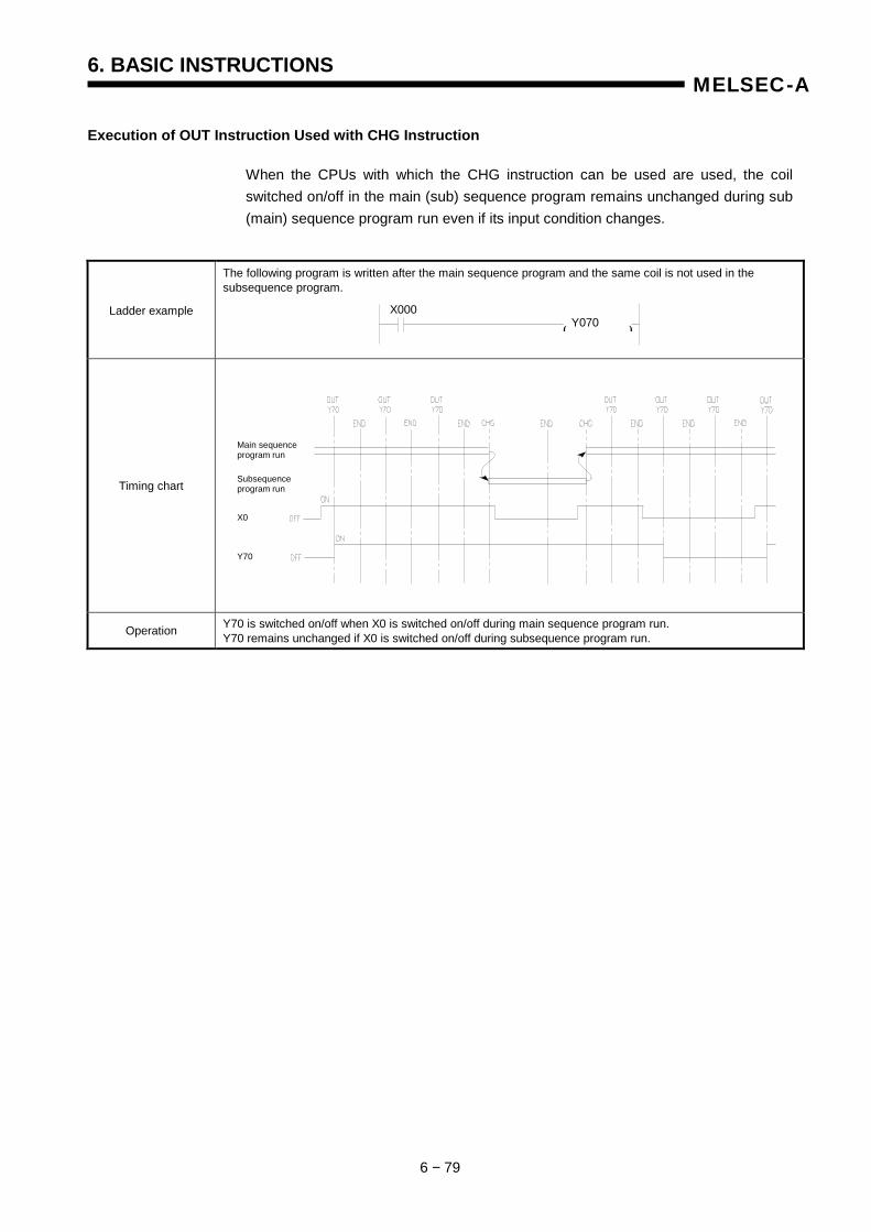
6. BASIC INSTRUCTIONS
6 − 79
MELSEC-A
Execution of OUT Instruction Used with CHG Instruction
When the CPUs with which the CHG instruction can be used are used, the coil switched on/off in the main (sub) sequence program remains unchanged during sub (main) sequence program run even if its input condition changes.
Ladder example
The following program is written after the main sequence program and the same coil is not used in the subsequence program.
Timing chart
Operation Y70 is switched on/off when X0 is switched on/off during main sequence program run. Y70 remains unchanged if X0 is switched on/off during subsequence program run.
( )
X000
Main sequence program run
Subsequence program run
X0
Y70
Y070
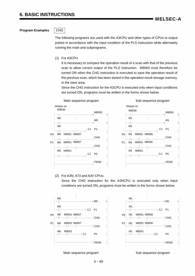
6. BASIC INSTRUCTIONS
6 − 80
MELSEC-A
Program Examples CHG
The following programs are used with the A3CPU and other types of CPUs to output pulses in accordance with the input condition of the PLS instruction while alternately running the main and subprograms.
(1) For A3CPU It is necessary to compare the operation result of a scan with that of the previous scan to allow correct output of the PLS instruction. M9050 must therefore be turned ON when the CHG instruction is executed to save the operation result of the previous scan, which has been stored in the operation result storage memory, in the save area. Since the CHG instruction for the A3CPU is executed only when input conditions are turned ON, programs must be written in the forms shown below.
(2) For A3N, A73 and A3V CPUs Since the CHG instruction for the A3NCPU is executed only when input conditions are turned ON, programs must be written in the forms shown below.
( )
( )
Main sequence program Sub sequence program
( )( )
( )
( )
M9036
M0
M0
M0
M0
M0
P0
P1
M9051
M9051
M9051
M9057
M9057
M9050
M0
CJ P1
CHG
CHG
CJ P0
FEND
Always on M9036
M1
M1
M1
M1
M1
P0
P1
M9051
M9051
M9051
M9056
M9056
M9050
M1
CJ P1
CHG
CHG
CJ P0
FEND
Always on
M0
M0
M0
M0
M0
P0
P1
M9051
M9051
M9051
M9057
M9057
M0
CJ P1
CHG
CHG
CJ P0
FEND
M1
M1
M1
M1
M1
P0
P1
M9051
M9051
M9051
M9056
M9056
M1
CJ P1
CHG
CHG
CJ P0
FEND
Main sequence program Sub sequence program
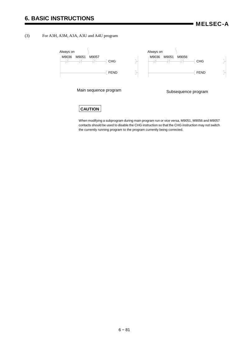
6. BASIC INSTRUCTIONS
6 − 81
MELSEC-A
(3) For A3H, A3M, A3A, A3U and A4U program
CAUTION
When modifying a subprogram during main program run or vice versa, M9051, M9056 and M9057 contacts should be used to disable the CHG instruction so that the CHG instruction may not switch the currently running program to the program currently being corrected.
Always on M9036 M9056 M9051
CHG
FEND
Always on M9036 M9057 M9051
CHG
FEND
Main sequence program Subsequence program
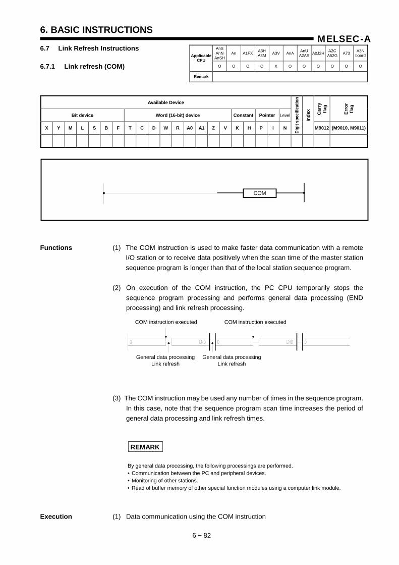
6. BASIC INSTRUCTIONS
6 − 82
MELSEC-A6.7 Link Refresh Instructions
6.7.1 Link refresh (COM)
Available Device
Bit device Word (16-bit) device Constant Pointer Level Car
ry
flag
Erro
r fla
g
X Y M L S B F T C D W R A0 A1 Z V K H P I N
Digi
t spe
cific
atio
n
Inde
x
M9012 (M9010, M9011)
Functions (1) The COM instruction is used to make faster data communication with a remote I/O station or to receive data positively when the scan time of the master station sequence program is longer than that of the local station sequence program.
(2) On execution of the COM instruction, the PC CPU temporarily stops the
sequence program processing and performs general data processing (END processing) and link refresh processing.
(3) The COM instruction may be used any number of times in the sequence program. In this case, note that the sequence program scan time increases the period of general data processing and link refresh times.
REMARK
By general data processing, the following processings are performed. • Communication between the PC and peripheral devices. • Monitoring of other stations. • Read of buffer memory of other special function modules using a computer link module.
Execution (1) Data communication using the COM instruction
AnSAnN
AnSHAn A1FX A3H
A3M A3V AnA AnU A2AS A0J2H A2C
A52G A73 A3NboardApplicable
CPU O O O O X O O O O O O
Remark
COM
COM instruction executed COM instruction executed
General data processingLink refresh
General data processingLink refresh
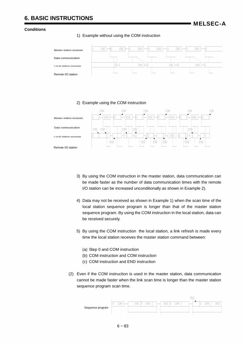
6. BASIC INSTRUCTIONS
6 − 83
MELSEC-AConditions
1) Example without using the COM instruction
2) Example using the COM instruction
3) By using the COM instruction in the master station, data communication can be made faster as the number of data communication times with the remote I/O station can be increased unconditionally as shown in Example 2).
4) Data may not be received as shown in Example 1) when the scan time of the
local station sequence program is longer than that of the master station sequence program. By using the COM instruction in the local station, data can be received securely.
5) By using the COM instruction the local station, a link refresh is made every
time the local station receives the master station command between: (a) Step 0 and COM instruction (b) COM instruction and COM instruction (c) COM instruction and END instruction
(2) Even if the COM instruction is used in the master station, data communication
cannot be made faster when the link scan time is longer than the master station sequence program scan time.
Master station program
Data communication
Local station program
Remote I/O station
Master station program
Data communication
Local station program
Remote I/O station
Sequence program
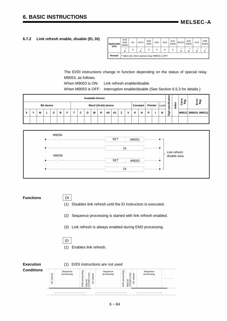
6. BASIC INSTRUCTIONS
6 − 84
MELSEC-A 6.7.2 Link refresh enable, disable (EI, DI)
The EI/DI instructions change in function depending on the status of special relay M9053, as follows. When M9053 is ON: Link refresh enable/disable When M9053 is OFF: Interruption enable/disable (See Section 6.5.3 for details.)
Available Device
Bit device Word (16-bit) device Constant Pointer Level Car
ry
flag
Erro
r fla
g
X Y M L S B F T C D W R A0 A1 Z V K H P I N
Digi
t spe
cific
atio
n
Inde
x
M9012 (M9010, M9011)
Functions DI (1) Disables link refresh until the EI instruction is executed. (2) Sequence processing is started with link refresh enabled. (3) Link refresh is always enabled during END processing.
EI
(1) Enables link refresh. Execution (1) EI/DI instructions are not used Conditions
AnSAnN
AnSHAn A1FX A3H
A3M A3V AnA AnU A2AS A0J2H A2C
A52G A73 A3NboardApplicable
CPU X X X X X
Remark * Valid only when special relay M9053 is OFF.
Link refresh disable area
SET
DI
M9036
M9036
M9053
SET
DI
M9053
Sequence processing
Sequence processing
Sequence processing
I/O re
fresh
END
pro
cess
ing
Wai
t for
co
nsta
nt s
can
I/O re
fresh
END
pro
cess
ing
Wai
t for
co
nsta
nt s
can
I/O re
fresh
* * * ** *
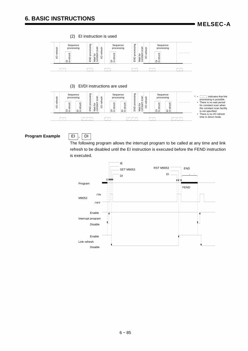
6. BASIC INSTRUCTIONS
6 − 85
MELSEC-A
(2) EI instruction is used
(3) EI/DI instructions are used Program Example EI , DI
The following program allows the interrupt program to be called at any time and link refresh to be disabled until the EI instruction is executed before the FEND instruction is executed.
Sequence processing
Sequence processing
Sequence processing
I/O re
fresh
END
pro
cess
ing
Wai
t for
co
nsta
nt s
can
I/O re
fresh
END
pro
cess
ing
Wai
t for
co
nsta
nt s
can
I/O re
fresh
DI
in-s
truct
i
DI
in-s
truct
i
DI
in-s
truct
i
Sequence processing
Sequence processing
Sequence processing
I/O re
fresh
END
pro
cess
ing
Wai
t for
co
nsta
nt s
can
I/O re
fresh
END
pro
cess
ing
Wai
t for
co
nsta
nt s
can
I/O re
fresh
DI
in-s
truct
i
DI
in-s
truct
i
DI
in-s
truct
i
EI
in-s
truct
i
EI
in-s
truct
i
EI
in-s
truct
i
*: • indicates that link processing is possible. • There is no wait period for constant scan when the constant scan facility is not specified. • There is no I/O refresh time in direct mode.
IE
SET M9053
DI
RST M9053
EI
END
i
FEND
0
Link refresh
Program
Interrupt program
M9053 OFF
ON
Disable
Enable
Disable
Enable
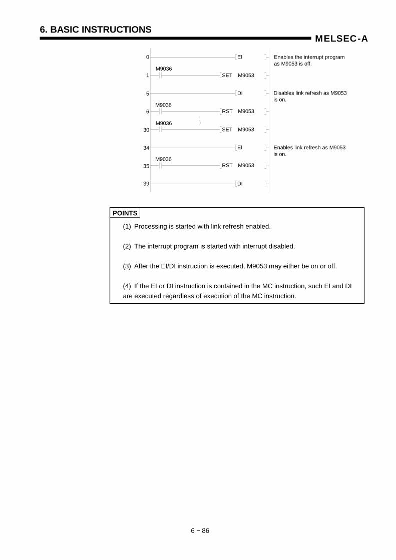
6. BASIC INSTRUCTIONS
6 − 86
MELSEC-A
POINTS
(1) Processing is started with link refresh enabled. (2) The interrupt program is started with interrupt disabled. (3) After the EI/DI instruction is executed, M9053 may either be on or off. (4) If the EI or DI instruction is contained in the MC instruction, such EI and DI are executed regardless of execution of the MC instruction.
SET M9053
EI
M9036
0
1
5
35
30
34
M9036
M9036
M9036
DI
RST M9053
EI
39 DI
SET M9053
RST M9053
Enables the interrupt program as M9053 is off.
Disables link refresh as M9053 is on.
Enables link refresh as M9053 is on.
6
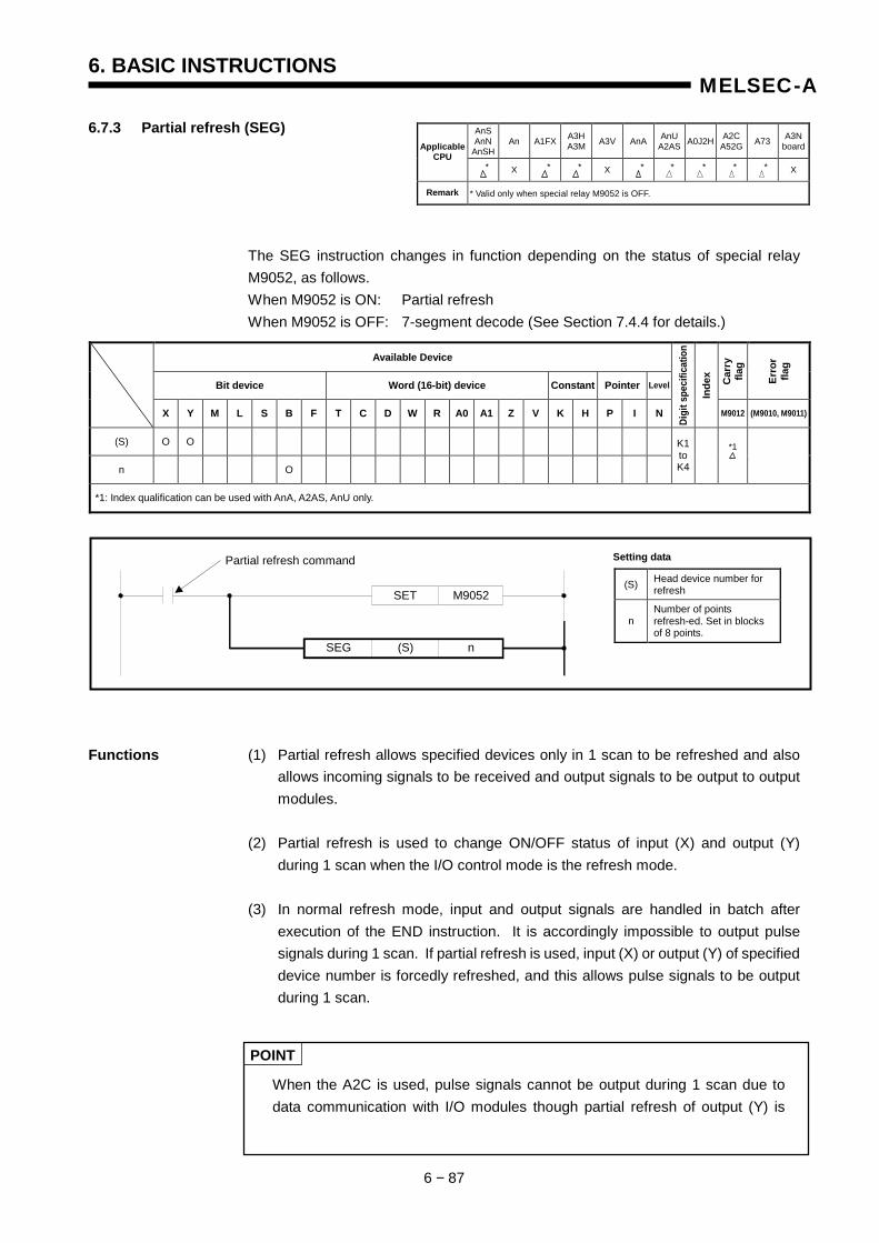
6. BASIC INSTRUCTIONS
6 − 87
MELSEC-A
6.7.3 Partial refresh (SEG)
The SEG instruction changes in function depending on the status of special relay M9052, as follows. When M9052 is ON: Partial refresh When M9052 is OFF: 7-segment decode (See Section 7.4.4 for details.)
Available Device
Bit device Word (16-bit) device Constant Pointer Level Car
ry
flag
Erro
r fla
g
X Y M L S B F T C D W R A0 A1 Z V K H P I N
Digi
t spe
cific
atio
n
Inde
x
M9012 (M9010, M9011)
(S) O O
n O
K1 to K4
*1: Index qualification can be used with AnA, A2AS, AnU only.
Functions (1) Partial refresh allows specified devices only in 1 scan to be refreshed and also allows incoming signals to be received and output signals to be output to output modules.
(2) Partial refresh is used to change ON/OFF status of input (X) and output (Y)
during 1 scan when the I/O control mode is the refresh mode. (3) In normal refresh mode, input and output signals are handled in batch after
execution of the END instruction. It is accordingly impossible to output pulse signals during 1 scan. If partial refresh is used, input (X) or output (Y) of specified device number is forcedly refreshed, and this allows pulse signals to be output during 1 scan.
POINT
When the A2C is used, pulse signals cannot be output during 1 scan due to data communication with I/O modules though partial refresh of output (Y) is
AnSAnN
AnSHAn A1FX A3H
A3M A3V AnA AnU A2AS A0J2H A2C
A52G A73 A3NboardApplicable
CPU X X X
Remark * Valid only when special relay M9052 is OFF.
* * * ** ** *
*1
SET M9052
SEG (S) n
Partial refresh command
(S) Head device number for refresh
n Number of points refresh-ed. Set in blocks of 8 points.
Setting data
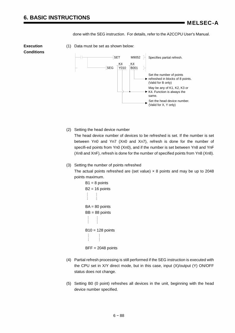
6. BASIC INSTRUCTIONS
6 − 88
MELSEC-A
done with the SEG instruction. For details, refer to the A2CCPU User's Manual. Execution (1) Data must be set as shown below: Conditions
(2) Setting the head device number The head device number of devices to be refreshed is set. If the number is set
between Yn0 and Yn7 (Xn0 and Xn7), refresh is done for the number of specifi-ed points from Yn0 (Xn0), and if the number is set between Yn8 and YnF (Xn8 and XnF), refresh is done for the number of specified points from Yn8 (Xn8).
(3) Setting the number of points refreshed The actual points refreshed are (set value) × 8 points and may be up to 2048
points maximum. B1 = 8 points B2 = 16 points BA = 80 points BB = 88 points B10 = 128 points BFF = 2048 points (4) Partial refresh processing is still performed if the SEG instruction is executed with
the CPU set in X/Y direct mode, but in this case, input (X)/output (Y) ON/OFF status does not change.
(5) Setting B0 (0 point) refreshes all devices in the unit, beginning with the head
device number specified.
K4 K4 SEG Y010 B001
SET M9052 Specifies partial refresh.
Set the number of points refreshed in blocks of 8 points. (Valid for B only) May be any of K1, K2, K3 or K4. Function is always the same. Set the head device number. (Valid for X, Y only)
……
……
……
……
……
……

6. BASIC INSTRUCTIONS
6 − 89
MELSEC-A
Program Examples SEG (1) The following example refreshes Y10 to Y27.
(2) Pulse output using the SET and RST instructions in direct mode should be changed as shown below when the I/O control is changed to refresh mode.
CAUTION
Pulse signals cannot be output using the programs above when the A2CPU is used.
K4 K4 SEG Y010 B003
SET M9052 X001
0 •••• Coding 0 LD X001 1 SET M9052 4 SEG K4Y010 K4B003 11 END
SET Y022 X001
0
RST Y022
K4 K4 SEG Y020 B001
SET M9052X001
0
SET Y022
K4 K4 SEG Y020 B001
RST Y022
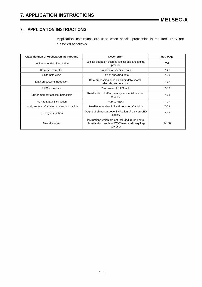
7. APPLICATION INSTRUCTIONS
7 − 1
MELSEC-A
7. APPLICATION INSTRUCTIONS
Application instructions are used when special processing is required. They are classified as follows:
Classification of Application Instructions Description Ref. Page
Logical operation instruction Logical operation such as logical add and logical product 7-2
Rotation instruction Rotation of specified data 7-21
Shift instruction Shift of specified data 7-30
Data processing instruction Data processing such as 16-bit data search, decode, and encode 7-37
FIFO instruction Read/write of FIFO table 7-53
Buffer memory access instruction Read/write of buffer memory in special function module 7-58
FOR to NEXT instruction FOR to NEXT 7-77
Local, remote I/O station access instruction Read/write of data in local, remote I/O station 7-79
Display instruction Output of character code, indication of data on LED display 7-92
Miscellaneous Instructions which are not included in the above classification, such as WDT reset and carry flag
set/reset 7-108
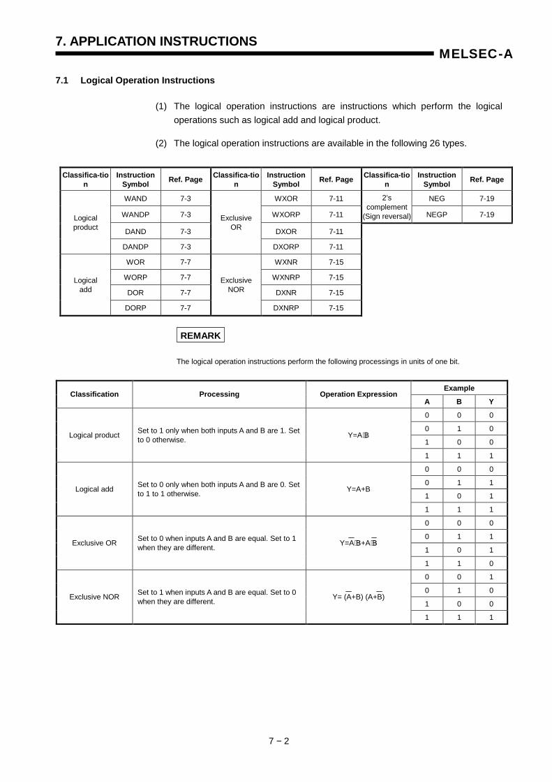
7. APPLICATION INSTRUCTIONS
7 − 2
MELSEC-A
7.1 Logical Operation Instructions
(1) The logical operation instructions are instructions which perform the logical operations such as logical add and logical product.
(2) The logical operation instructions are available in the following 26 types.
Classifica-tio
n Instruction
Symbol Ref. Page Classifica-tion
Instruction Symbol Ref. Page Classifica-tio
n Instruction
Symbol Ref. Page
WAND 7-3 WXOR 7-11 NEG 7-19
WANDP 7-3 WXORP 7-11
2’s complement
(Sign reversal) NEGP 7-19
DAND 7-3 DXOR 7-11
Logical product
DANDP 7-3
Exclusive OR
DXORP 7-11
WOR 7-7 WXNR 7-15
WORP 7-7 WXNRP 7-15
DOR 7-7 DXNR 7-15 Logical
add
DORP 7-7
Exclusive NOR
DXNRP 7-15
REMARK
The logical operation instructions perform the following processings in units of one bit.
Example Classification Processing Operation Expression
A B Y
0 0 0
0 1 0
1 0 0 Logical product Set to 1 only when both inputs A and B are 1. Set
to 0 otherwise. Y=A⋅B
1 1 1
0 0 0
0 1 1
1 0 1 Logical add Set to 0 only when both inputs A and B are 0. Set
to 1 to 1 otherwise. Y=A+B
1 1 1
0 0 0
0 1 1
1 0 1 Exclusive OR Set to 0 when inputs A and B are equal. Set to 1
when they are different. Y=A⋅B+A⋅B
1 1 0
0 0 1
0 1 0
1 0 0 Exclusive NOR Set to 1 when inputs A and B are equal. Set to 0
when they are different. Y= (A+B) (A+B)
1 1 1

7. APPLICATION INSTRUCTIONS
7 − 3
MELSEC-A
7.1.1 16-, 32-bit data logical product (WAND, WANDP, DAND, DANDP)
Available Device
Bit device Word (16-bit) device Constant Pointer Level Car
ry
flag
Erro
r fla
g
X Y M L S B F T C D W R A0 A1 Z V K H P I N
Digi
t spe
cific
atio
n
Inde
x
M9012 (M9010, M9011)
(S) O O O O O O O O O O O O O O O O O O
(D) O O O O O O O O O O O O O O O
(S1) O O O O O O O O O O O O O O O O O O
(S2) O O O O O O O O O O O O O O O O O O
WAND
(D1) O O O O O O O O O O O O O O O
K1
to
K4
(S) O O O O O O O O O O O O O O O O DAND
(D) O O O O O O O O O O O O O
K1 to K8
O O
Functions WAND (1) Performs the logical product of the 16-bit data of device specified at (D) and the
16-bit data of device specified at (S) per bit, and stores the result into the device specified at (D).
Applicable CPU All CPUs
16 bits
WAND Before execution
After execution
(S) (D)
(S) (D)P (S)
(S1)
(S2)
(D)
Data for which logical product will be performed or head number of device which stores data
(D1) Head number of device which will store the result of logical product
Setting data
WAND, DAND
Indicates the instruction symbol.
Operation commands
(S1) (D1)
(S1) (D1)P
(S2)
(S2) WAND may only be used in the areas marked *.
Operation commands
*
*
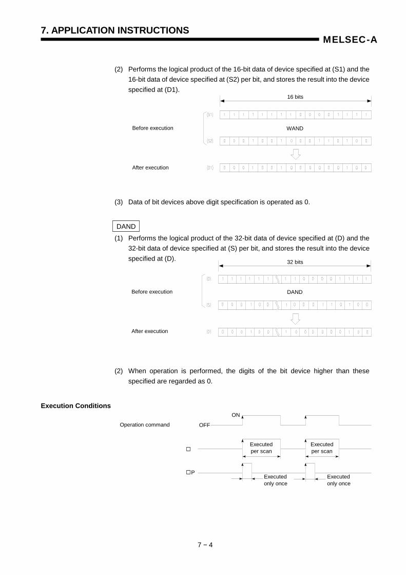
7. APPLICATION INSTRUCTIONS
7 − 4
MELSEC-A
(2) Performs the logical product of the 16-bit data of device specified at (S1) and the
16-bit data of device specified at (S2) per bit, and stores the result into the device specified at (D1).
(3) Data of bit devices above digit specification is operated as 0.
DAND
(1) Performs the logical product of the 32-bit data of device specified at (D) and the 32-bit data of device specified at (S) per bit, and stores the result into the device specified at (D).
(2) When operation is performed, the digits of the bit device higher than these specified are regarded as 0.
Execution Conditions
16 bits
WAND Before execution
After execution
32 bits
DAND Before execution
After execution
OFF
ON
Executed per scan
Executed per scan
Executed only once
Executed only once
P
Operation command
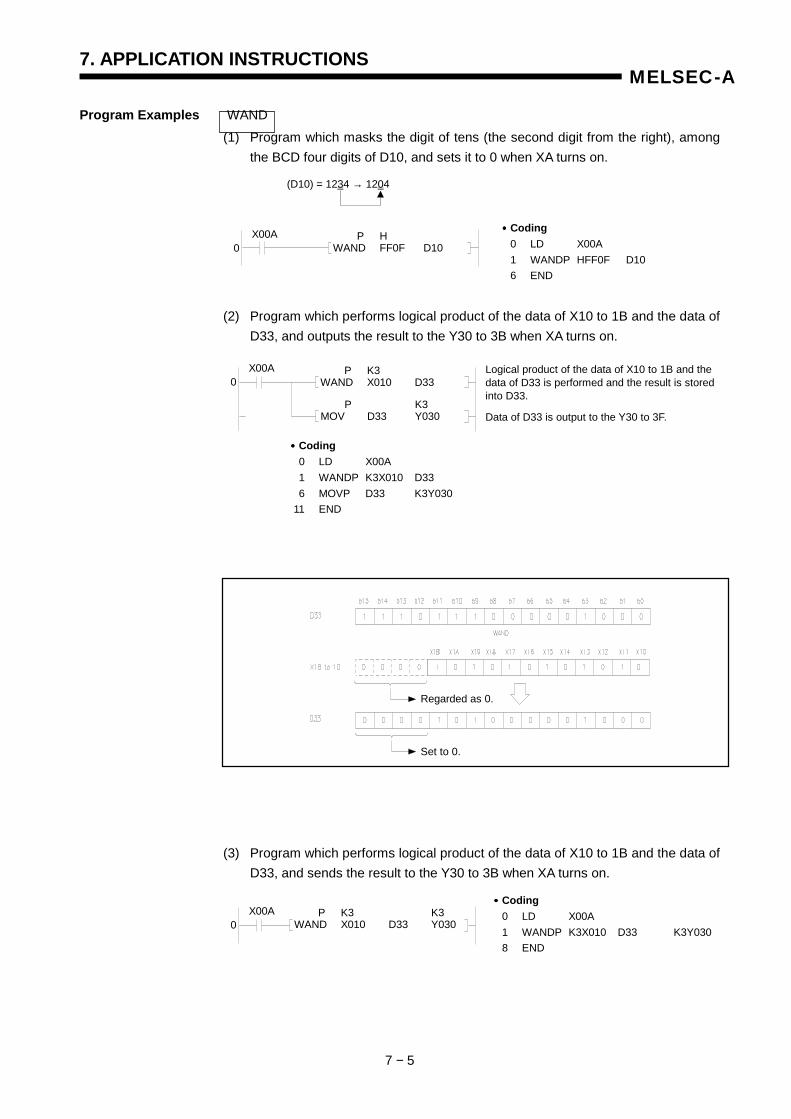
7. APPLICATION INSTRUCTIONS
7 − 5
MELSEC-A
Program Examples WAND (1) Program which masks the digit of tens (the second digit from the right), among
the BCD four digits of D10, and sets it to 0 when XA turns on.
(2) Program which performs logical product of the data of X10 to 1B and the data of
D33, and outputs the result to the Y30 to 3B when XA turns on.
(3) Program which performs logical product of the data of X10 to 1B and the data of D33, and sends the result to the Y30 to 3B when XA turns on.
(D10) = 1234 → 1204
X00A 0
P H WAND FF0F D10
•••• Coding 0 LD X00A 1 WANDP HFF0F D10 6 END
X00A 0
P K3 WAND X010 D33
P K3 MOV D33 Y030
Logical product of the data of X10 to 1B and the data of D33 is performed and the result is stored into D33.
Data of D33 is output to the Y30 to 3F.
•••• Coding 0 LD X00A 1 WANDP K3X010 D33 6 MOVP D33 K3Y030 11 END
Regarded as 0.
Set to 0.
X00A 0
P K3 K3 WAND X010 D33 Y030
•••• Coding 0 LD X00A 1 WANDP K3X010 D33 K3Y030 8 END

7. APPLICATION INSTRUCTIONS
7 − 6
MELSEC-A
DAND
(1) Program which performs logical product of the 24-bit data of X30 to 47 and the data of D99 and 100, then transfers the result to the M80 to 103 when X8 turns on.
(2) Program which performs logical product of the 32-bit data of D0 and 1 and the 32-bit data of D108 and 109, and sends the result to the Y100 to 11F when M16 turns on.
Regarded as 0.
Do not change.
X008 0
P K6 DAND X030 D99
P K6 DMOV D99 M80
Logical product of the data of X30 to47 and the data of D99 and 100 is performed and the result is stored into D99 and 100.
Data of D99 and 100 is transferred to the M80 to 103.
•••• Coding 0 LD X008 1 DANDP K6X030 D99 10 DMOVP D99 K6M80 17 END
Regarded as 0.
Set to 0.
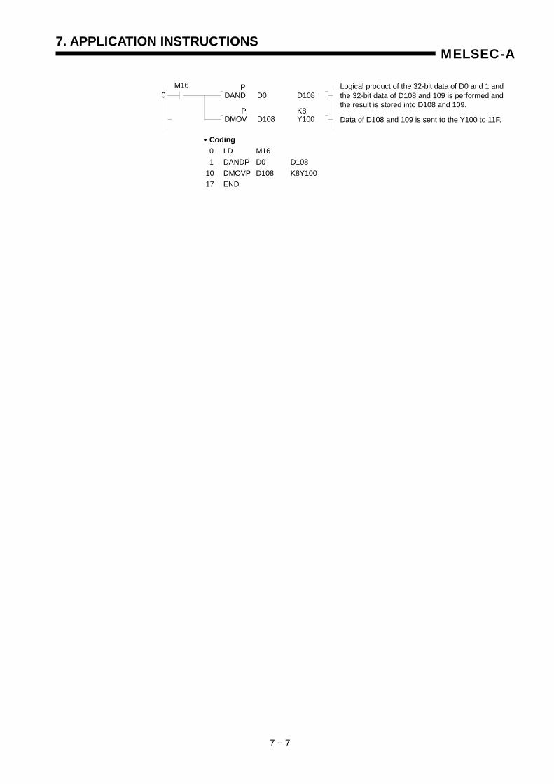
7. APPLICATION INSTRUCTIONS
7 − 7
MELSEC-A
M16 0
P DAND D0 D108
P K8 DMOV D108 Y100
Logical product of the 32-bit data of D0 and 1 and the 32-bit data of D108 and 109 is performed and the result is stored into D108 and 109.
Data of D108 and 109 is sent to the Y100 to 11F.
•••• Coding 0 LD M16 1 DANDP D0 D108 10 DMOVP D108 K8Y100 17 END
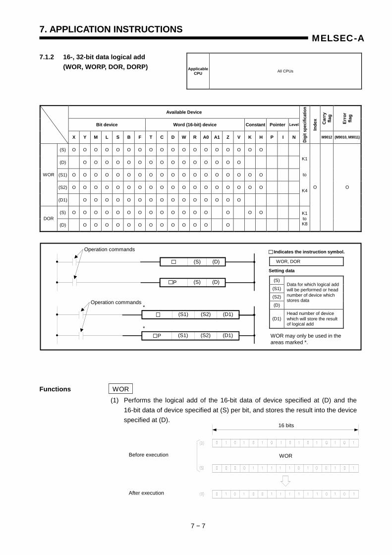
7. APPLICATION INSTRUCTIONS
7 − 7
MELSEC-A
7.1.2 16-, 32-bit data logical add (WOR, WORP, DOR, DORP)
Available Device
Bit device Word (16-bit) device Constant Pointer Level Car
ry
flag
Erro
r fla
g
X Y M L S B F T C D W R A0 A1 Z V K H P I N
Digi
t spe
cific
atio
n
Inde
x
M9012 (M9010, M9011)
(S) O O O O O O O O O O O O O O O O O O
(D) O O O O O O O O O O O O O O O
(S1) O O O O O O O O O O O O O O O O O O
(S2) O O O O O O O O O O O O O O O O O O
WOR
(D1) O O O O O O O O O O O O O O O
K1
to
K4
(S) O O O O O O O O O O O O O O O O DOR
(D) O O O O O O O O O O O O O
K1 to K8
O O
Functions WOR (1) Performs the logical add of the 16-bit data of device specified at (D) and the
16-bit data of device specified at (S) per bit, and stores the result into the device specified at (D).
Applicable CPU All CPUs
(S) (D)
(S) (D)P (S)
(S1)
(S2)
(D)
Data for which logical add will be performed or head number of device which stores data
(D1) Head number of device which will store the result of logical add
Setting data
WOR, DOR
Indicates the instruction symbol.
Operation commands
(S1) (D1)
(S1) (D1)P
(S2)
(S2) WOR may only be used in the areas marked *.
Operation commands
*
*
16 bits
WOR Before execution
After execution
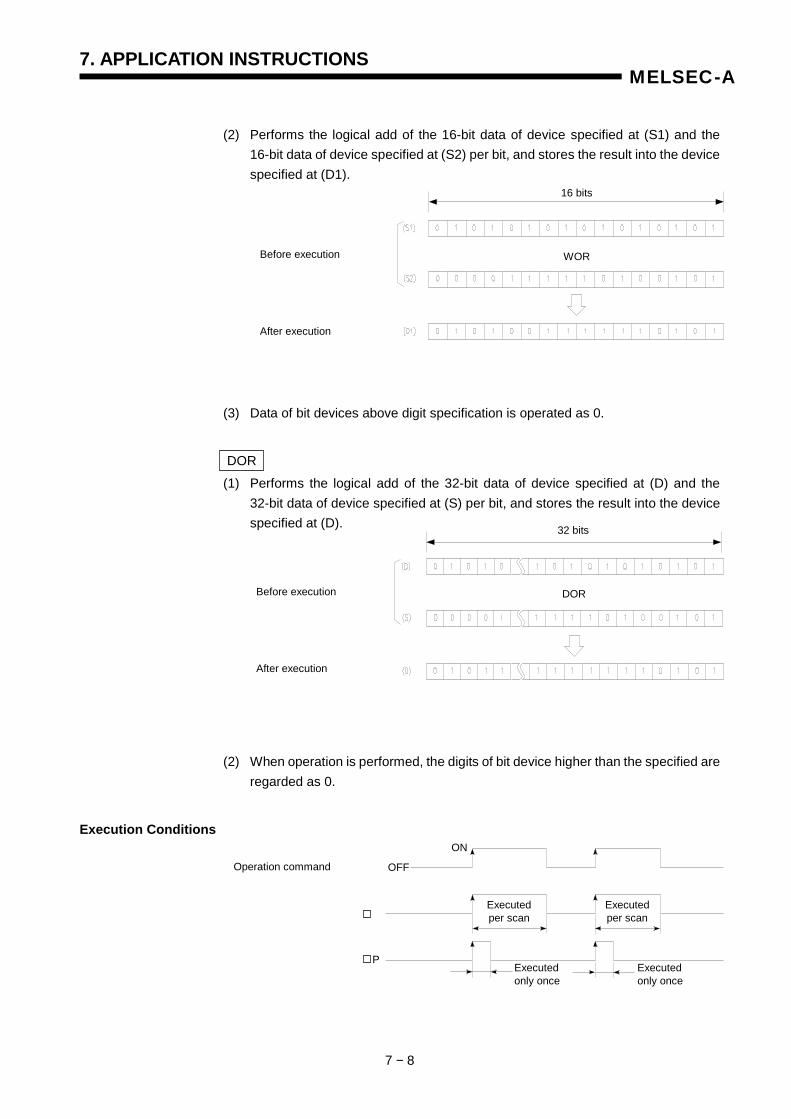
7. APPLICATION INSTRUCTIONS
7 − 8
MELSEC-A
(2) Performs the logical add of the 16-bit data of device specified at (S1) and the
16-bit data of device specified at (S2) per bit, and stores the result into the device specified at (D1).
(3) Data of bit devices above digit specification is operated as 0.
DOR (1) Performs the logical add of the 32-bit data of device specified at (D) and the
32-bit data of device specified at (S) per bit, and stores the result into the device specified at (D).
(2) When operation is performed, the digits of bit device higher than the specified are regarded as 0.
Execution Conditions
16 bits
WOR Before execution
After execution
32 bits
DOR Before execution
After execution
OFF
ON
Executed per scan
Executed per scan
Executed only once
Executed only once
P
Operation command
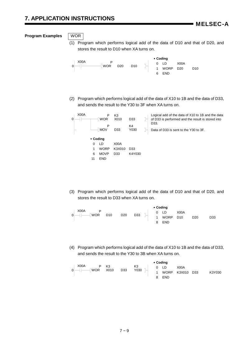
7. APPLICATION INSTRUCTIONS
7 − 9
MELSEC-A
Program Examples WOR (1) Program which performs logical add of the data of D10 and that of D20, and
stores the result to D10 when XA turns on.
(2) Program which performs logical add of the data of X10 to 1B and the data of D33, and sends the result to the Y30 to 3F when XA turns on.
(3) Program which performs logical add of the data of D10 and that of D20, and stores the result to D33 when XA turns on.
(4) Program which performs logical add of the data of X10 to 1B and the data of D33, and sends the result to the Y30 to 3B when XA turns on.
X00A 0
P WOR D20 D10
•••• Coding 0 LD X00A 1 WORP D20 D10 6 END
X00A 0
P K3 WOR X010 D33
P K4 MOV D33 Y030
Logical add of the data of X10 to 1B and the data of D33 is performed and the result is stored into D33.
Data of D33 is sent to the Y30 to 3F.
•••• Coding 0 LD X00A 1 WORP K3X010 D33 6 MOVP D33 K4Y030 11 END
X00A 0
P WOR D10 D20 D33
•••• Coding 0 LD X00A 1 WORP D10 D20 D33 8 END
X00A 0
P K3 K3 WOR X010 D33 Y030
•••• Coding 0 LD X00A 1 WORP K3X010 D33 K3Y030 8 END
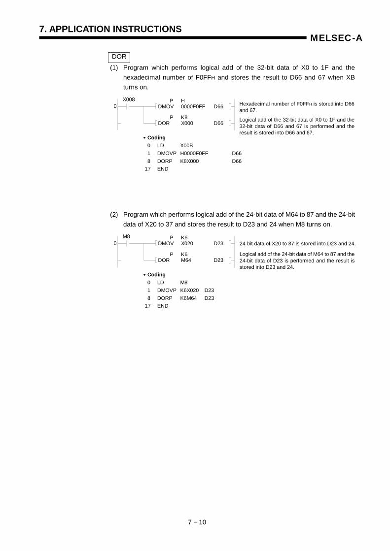
7. APPLICATION INSTRUCTIONS
7 − 10
MELSEC-A
DOR (1) Program which performs logical add of the 32-bit data of X0 to 1F and the
hexadecimal number of F0FFH and stores the result to D66 and 67 when XB turns on.
(2) Program which performs logical add of the 24-bit data of M64 to 87 and the 24-bit data of X20 to 37 and stores the result to D23 and 24 when M8 turns on.
X008 0
P H DMOV 0000F0FF D66
P K8 DOR X000 D66
Hexadecimal number of F0FFH is stored into D66 and 67.
Logical add of the 32-bit data of X0 to 1F and the 32-bit data of D66 and 67 is performed and the result is stored into D66 and 67.
•••• Coding 0 LD X00B 1 DMOVP H0000F0FF D66 8 DORP K8X000 D66 17 END
M8 0
P K6 DMOV X020 D23
P K6 DOR M64 D23
24-bit data of X20 to 37 is stored into D23 and 24.
Logical add of the 24-bit data of M64 to 87 and the24-bit data of D23 is performed and the result is stored into D23 and 24.
•••• Coding 0 LD M8 1 DMOVP K6X020 D23 8 DORP K6M64 D23 17 END

7. APPLICATION INSTRUCTIONS
7 − 11
MELSEC-A
7.1.3 16-, 32-bit data exclusive logical add (WXOR, WXORP, DXOR, DXORP)
Available Device
Bit device Word (16-bit) device Constant Pointer Level Car
ry
flag
Erro
r fla
g
X Y M L S B F T C D W R A0 A1 Z V K H P I N
Digi
t spe
cific
atio
n
Inde
x
M9012 (M9010, M9011)
(S) O O O O O O O O O O O O O O O O O O
(D) O O O O O O O O O O O O O O O
(S1) O O O O O O O O O O O O O O O O O O
(S2) O O O O O O O O O O O O O O O O O O
WXOR
(D1) O O O O O O O O O O O O O O O
K1
to
K4
(S) O O O O O O O O O O O O O O O O DXOR
(D) O O O O O O O O O O O O O
K1 to K8
O O
Functions WXOR (1) Performs the exclusive OR of the 16-bit data of device specified at (D) and the
16-bit data of device specified at (S) per bit, and stores the result into the device specified at (D).
Applicable CPU All CPUs
(S) (D)
(S) (D)P (S)
(S1)
(S2)
(D)
Data for which exclusive OR will be performed or head number of device which stores data
(D1) Head number of device which will store the result of exclusive OR
Setting data
WXOR, DXOR
Indicates the instruction symbol.
Operation commands
(S1) (D1)
(S1) (D1)P
(S2)
(S2) WXOR may only be used in the areas marked *.
Operation commands
*
*
16 bits
WXOR Before execution
After execution
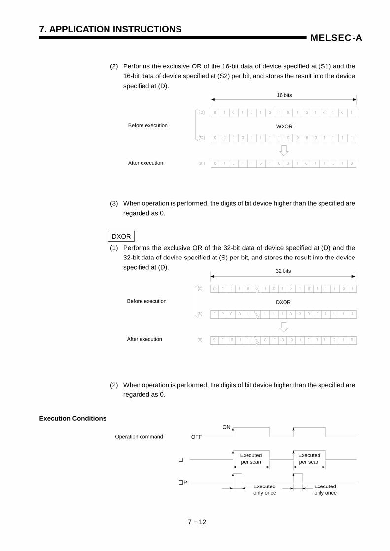
7. APPLICATION INSTRUCTIONS
7 − 12
MELSEC-A
(2) Performs the exclusive OR of the 16-bit data of device specified at (S1) and the
16-bit data of device specified at (S2) per bit, and stores the result into the device specified at (D).
(3) When operation is performed, the digits of bit device higher than the specified are regarded as 0.
DXOR
(1) Performs the exclusive OR of the 32-bit data of device specified at (D) and the 32-bit data of device specified at (S) per bit, and stores the result into the device specified at (D).
(2) When operation is performed, the digits of bit device higher than the specified are regarded as 0.
Execution Conditions
16 bits
WXOR Before execution
After execution
32 bits
DXOR Before execution
After execution
OFF
ON
Executed per scan
Executed per scan
Executed only once
Executed only once
P
Operation command
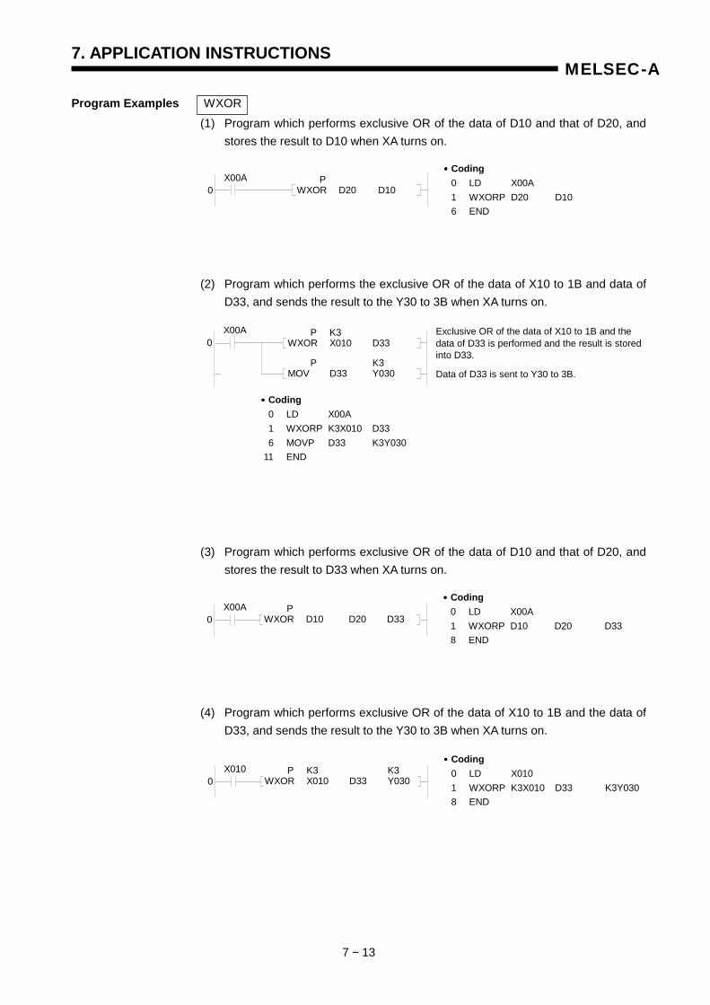
7. APPLICATION INSTRUCTIONS
7 − 13
MELSEC-A
Program Examples WXOR (1) Program which performs exclusive OR of the data of D10 and that of D20, and
stores the result to D10 when XA turns on.
(2) Program which performs the exclusive OR of the data of X10 to 1B and data of D33, and sends the result to the Y30 to 3B when XA turns on.
(3) Program which performs exclusive OR of the data of D10 and that of D20, and stores the result to D33 when XA turns on.
(4) Program which performs exclusive OR of the data of X10 to 1B and the data of D33, and sends the result to the Y30 to 3B when XA turns on.
X00A 0
P WXOR D20 D10
•••• Coding 0 LD X00A 1 WXORP D20 D10 6 END
X00A 0
P K3 WXOR X010 D33
P K3 MOV D33 Y030
Exclusive OR of the data of X10 to 1B and the data of D33 is performed and the result is stored into D33.
Data of D33 is sent to Y30 to 3B.
•••• Coding 0 LD X00A 1 WXORP K3X010 D33 6 MOVP D33 K3Y030 11 END
X00A 0
P WXOR D10 D20 D33
•••• Coding 0 LD X00A 1 WXORP D10 D20 D33 8 END
X010 0
P K3 K3 WXOR X010 D33 Y030
•••• Coding 0 LD X010 1 WXORP K3X010 D33 K3Y030 8 END
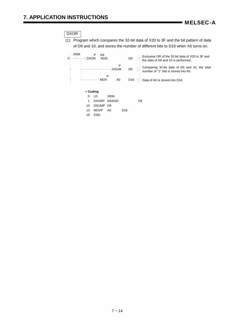
7. APPLICATION INSTRUCTIONS
7 − 14
MELSEC-A
DXOR (1) Program which compares the 32-bit data of X20 to 3F and the bit pattern of data
of D9 and 10, and stores the number of different bits to D16 when X6 turns on.
X006 0
P K8 DXOR X020 D9
P DSUM D9
Exclusive OR of the 32-bit data of X20 to 3F and the data of D9 and 10 is performed.
Comparing 32-bit data of D9 and 10, the total number of "1" bits is stored into A0.
•••• Coding 0 LD X006 1 DXORP K8X020 D9 10 DSUMP D9 13 MOVP A0 D16 18 END
P MOV A0 D16 Data of A0 is stored into D16.
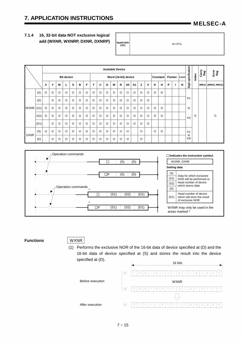
7. APPLICATION INSTRUCTIONS
7 − 15
MELSEC-A
7.1.4 16, 32-bit data NOT exclusive logical add (WXNR, WXNRP, DXNR, DXNRP)
Available Device
Bit device Word (16-bit) device Constant Pointer Level Car
ry
flag
Erro
r fla
g
X Y M L S B F T C D W R A0 A1 Z V K H P I N
Digi
t spe
cific
atio
n
Inde
x
M9012 (M9010, M9011)
(S) O O O O O O O O O O O O O O O O O O
(D) O O O O O O O O O O O O O O O
(S1) O O O O O O O O O O O O O O O O O O
(S2) O O O O O O O O O O O O O O O O O O
WXNR
(D1) O O O O O O O O O O O O O O O
K1
to
K4
(S) O O O O O O O O O O O O O O O O DXNR
(D) O O O O O O O O O O O O O
K1 to K8
O O
Functions WXNR (1) Performs the exclusive NOR of the 16-bit data of device specified at (D) and the
16-bit data of device specified at (S) and stores the result into the device specified at (D).
Applicable CPU All CPUs
(S) (D)
(S) (D)P (S)
(S1)
(S2)
(D)
Data for which exclusive NOR will be performed or head number of device which stores data
(D1) Head number of device which will store the result of exclusive NOR
Setting data
WXNR, DXNR
Indicates the instruction symbol.
Operation commands
(S1) (D1)
(S1) (D1)P
(S2)
(S2) WXNR may only be used in theareas marked *
Operation commands
*
*
16 bits
WXNR Before execution
After execution
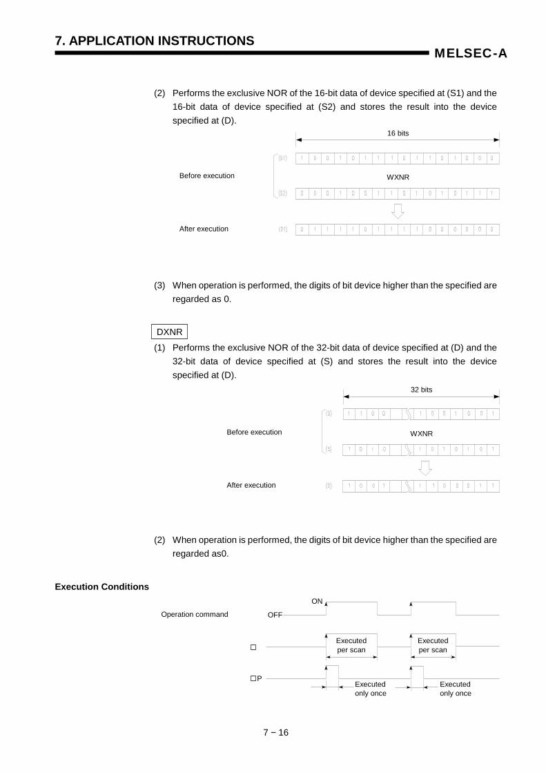
7. APPLICATION INSTRUCTIONS
7 − 16
MELSEC-A
(2) Performs the exclusive NOR of the 16-bit data of device specified at (S1) and the
16-bit data of device specified at (S2) and stores the result into the device specified at (D).
(3) When operation is performed, the digits of bit device higher than the specified are regarded as 0.
DXNR
(1) Performs the exclusive NOR of the 32-bit data of device specified at (D) and the 32-bit data of device specified at (S) and stores the result into the device specified at (D).
(2) When operation is performed, the digits of bit device higher than the specified are regarded as0.
Execution Conditions
16 bits
WXNR Before execution
After execution
32 bits
WXNR Before execution
After execution
OFF
ON
Executed per scan
Executed per scan
Executed only once
Executed only once
P
Operation command
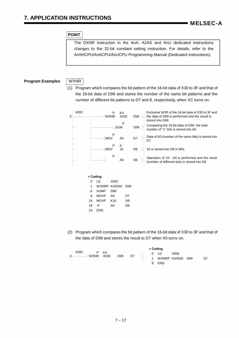
7. APPLICATION INSTRUCTIONS
7 − 17
MELSEC-A
POINT
The DXNR instruction in the AnA, A2AS and AnU dedicated instructions changes to the 32-bit constant setting instruction. For details, refer to the AnSHCPU/AnACPU/AnUCPU Programming Manual (Dedicated Instructions).
Program Examples WXNR (1) Program which compares the bit pattern of the 16-bit data of X30 to 3F and that of
the 16-bit data of D99 and stores the number of the same bit patterns and the number of different bit patterns to D7 and 8, respectively, when XC turns on.
(2) Program which compares the bit pattern of the 16-bit data of X30 to 3F and that of the data of D99 and stores the result to D7 when X0 turns on.
X00C 0
P SUM D99
Exclusive NOR of the 16-bit data of X30 to 3F and the data of D99 is performed and the result is stored into D99. Comparing the 16-bit data of D99, the total number of "1" bits is stored into A0.
•••• Coding 0 LD X00C 1 WXNRP K4X030 D99 6 SUMP D99 9 MOVP A0 D7 14 MOVP K16 D8 19 -P A0 D8 24 END
Data of A0 (number of the same bits) is stored into D7.
P K4 WXNR X030 D99
P MOV A0 D7
P K MOV 16 D8
P - A0 D8 Operation of 16 - A0 is performed and the result
(number of different bits) is stored into D8.
16 is stored into D8 in BIN.
X000 0
P K4 WXNR X030 D99 D7
•••• Coding 0 LD X000 1 WXNRP K4X030 D99 D7 8 END
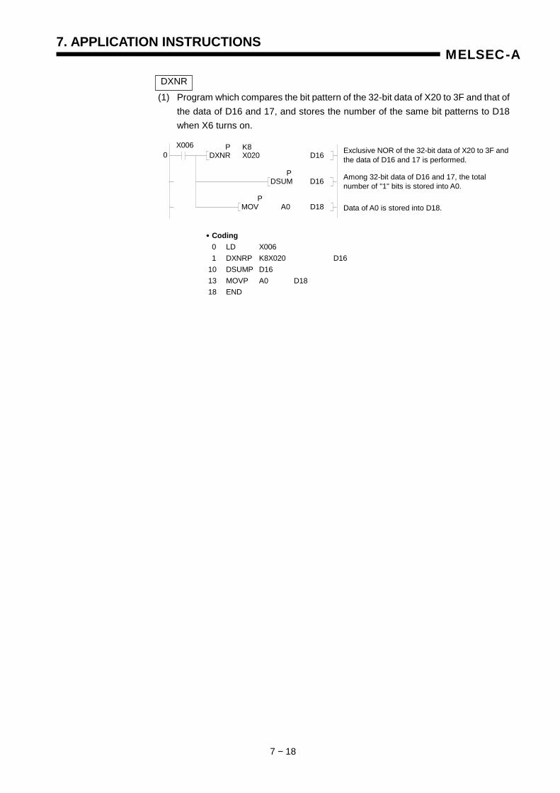
7. APPLICATION INSTRUCTIONS
7 − 18
MELSEC-A
DXNR (1) Program which compares the bit pattern of the 32-bit data of X20 to 3F and that of
the data of D16 and 17, and stores the number of the same bit patterns to D18 when X6 turns on.
X006 0
P K8 DXNR X020 D16
P DSUM D16
Exclusive NOR of the 32-bit data of X20 to 3F and the data of D16 and 17 is performed.
Among 32-bit data of D16 and 17, the total number of "1" bits is stored into A0.
•••• Coding 0 LD X006 1 DXNRP K8X020 D16 10 DSUMP D16 13 MOVP A0 D18 18 END
P MOV A0 D18 Data of A0 is stored into D18.
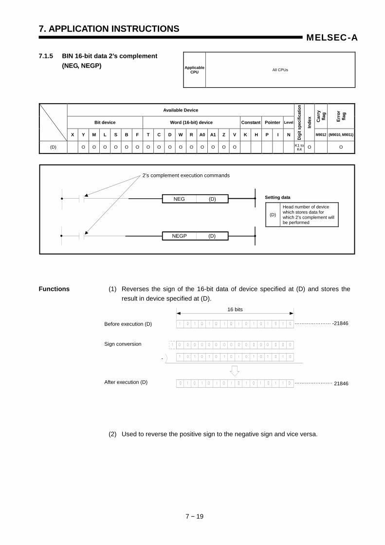
7. APPLICATION INSTRUCTIONS
7 − 19
MELSEC-A
7.1.5 BIN 16-bit data 2’s complement (NEG, NEGP)
Available Device
Bit device Word (16-bit) device Constant Pointer Level Car
ry
flag
Erro
r fla
g
X Y M L S B F T C D W R A0 A1 Z V K H P I N
Digi
t spe
cific
atio
n
Inde
x
M9012 (M9010, M9011)
(D) O O O O O O O O O O O O O O O O O
Functions (1) Reverses the sign of the 16-bit data of device specified at (D) and stores the result in device specified at (D).
(2) Used to reverse the positive sign to the negative sign and vice versa.
Applicable CPU All CPUs
K1 to K4
(D)
Head number of device which stores data for which 2’s complement will be performed
Setting data
2’s complement execution commands
(D) NEG
(D) NEGP
16 bits
-21846
21846
…………………
………………….
Before execution (D)
After execution (D)
Sign conversion
-
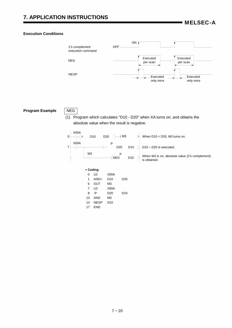
7. APPLICATION INSTRUCTIONS
7 − 20
MELSEC-A
Execution Conditions Program Example NEG
(1) Program which calculates "D10 - D20" when XA turns on, and obtains the absolute value when the result is negative.
OFF ON
Executed per scan
Executed per scan
Executed only once
Executed only once
NEG
NEGP
2’s complement execution command
( )X00A
0 < D10 D20
P - D20 D10
When D10 < D20, M3 turns on.
D10 – D20 is executed.
•••• Coding 0 LD X00A 1 AND< D10 D20 6 OUT M3 7 LD X00A 8 -P D20 D10 13 AND M3 14 NEGP D10 17 END
P NEG D10 When M3 is on, absolute value (2’s complement)
is obtained.
M3
X00A 7
M3
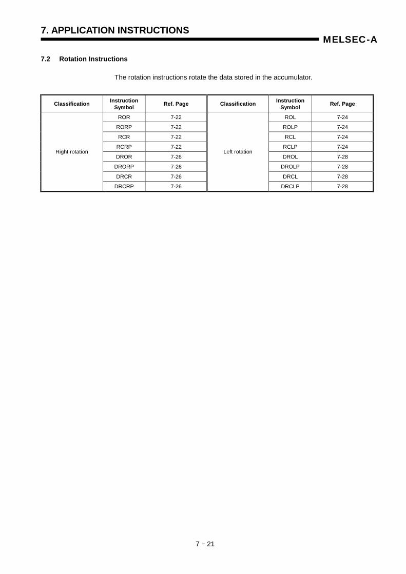
7. APPLICATION INSTRUCTIONS
7 − 21
MELSEC-A
7.2 Rotation Instructions
The rotation instructions rotate the data stored in the accumulator.
Classification Instruction Symbol Ref. Page Classification Instruction
Symbol Ref. Page
ROR 7-22 ROL 7-24
RORP 7-22 ROLP 7-24
RCR 7-22 RCL 7-24
RCRP 7-22 RCLP 7-24
DROR 7-26 DROL 7-28
DRORP 7-26 DROLP 7-28
DRCR 7-26 DRCL 7-28
Right rotation
DRCRP 7-26
Left rotation
DRCLP 7-28
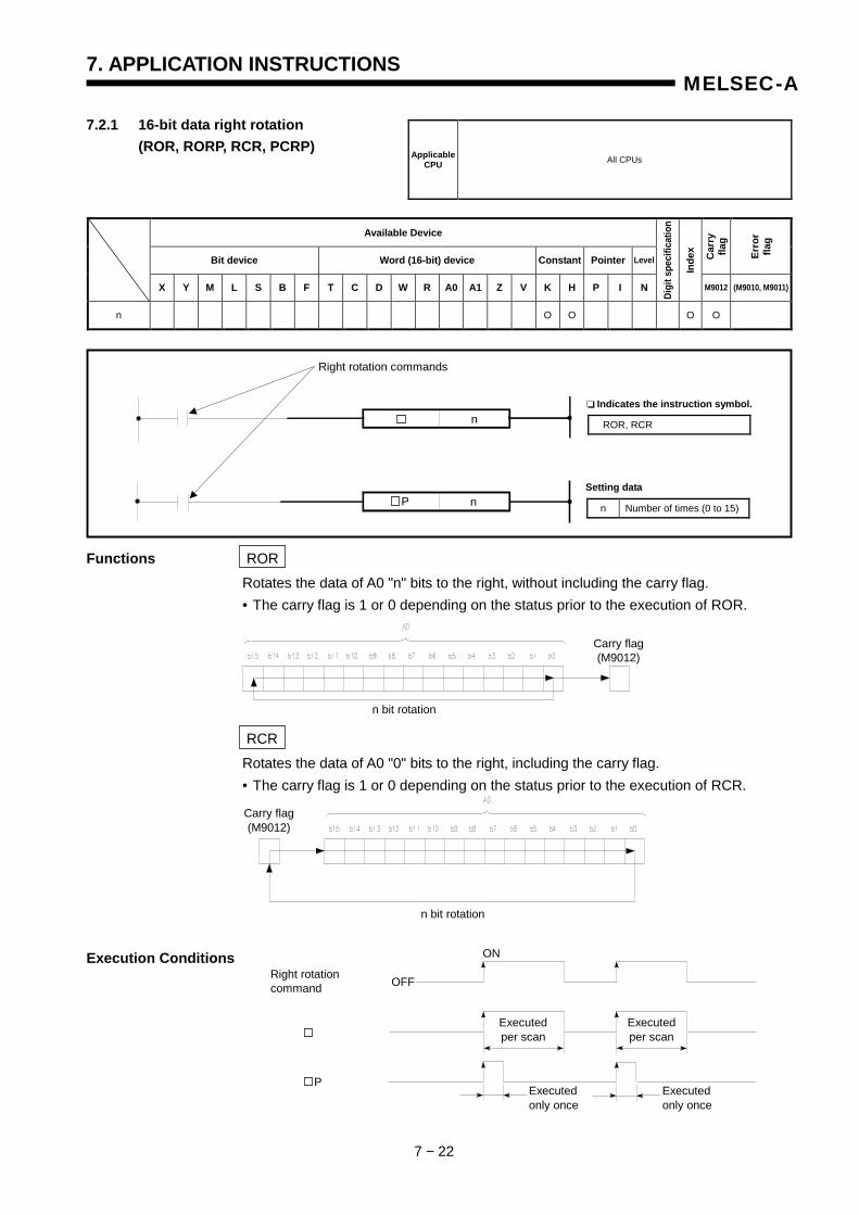
7. APPLICATION INSTRUCTIONS
7 − 22
MELSEC-A
7.2.1 16-bit data right rotation (ROR, RORP, RCR, PCRP)
Available Device
Bit device Word (16-bit) device Constant Pointer Level Car
ry
flag
Erro
r fla
g
X Y M L S B F T C D W R A0 A1 Z V K H P I N
Digi
t spe
cific
atio
n
Inde
x
M9012 (M9010, M9011)
n O O O O
Functions ROR Rotates the data of A0 "n" bits to the right, without including the carry flag. • The carry flag is 1 or 0 depending on the status prior to the execution of ROR.
RCR Rotates the data of A0 "0" bits to the right, including the carry flag. • The carry flag is 1 or 0 depending on the status prior to the execution of RCR.
Execution Conditions
Applicable CPU All CPUs
Carry flag (M9012)
n bit rotation
Carry flag (M9012)
n bit rotation
ON
OFF
Executed per scan
Executed per scan
Executed only once
Executed only once
Right rotation command
P
Right rotation commands
n
n
ROR, RCR
❏ Indicates the instruction symbol.
n Number of times (0 to 15)
Setting data P
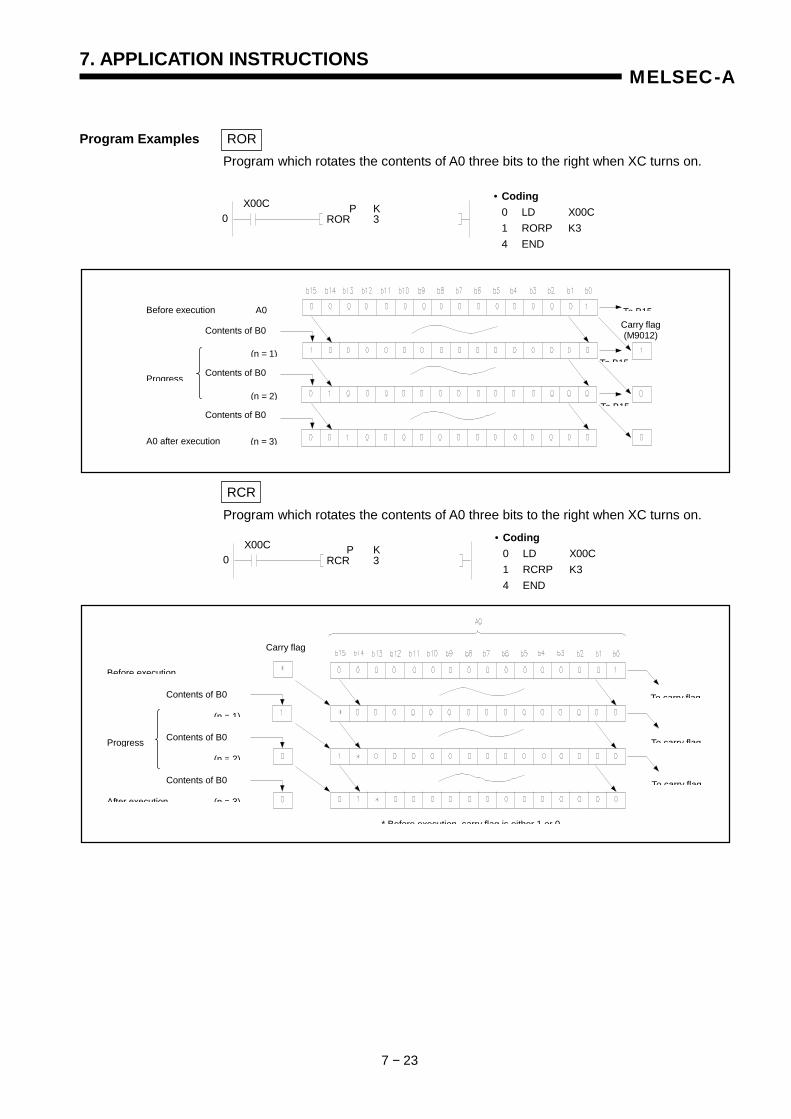
7. APPLICATION INSTRUCTIONS
7 − 23
MELSEC-A
Program Examples ROR Program which rotates the contents of A0 three bits to the right when XC turns on.
RCR Program which rotates the contents of A0 three bits to the right when XC turns on.
X00C P KROR 3 0
• Coding 0 LD X00C 1 RORP K3 4 END
X00C P KRCR 3 0
• Coding 0 LD X00C 1 RCRP K3 4 END
To carry flag
To carry flag
To carry flag
* Before execution carry flag is either 1 or 0
Carry flag
Contents of B0
(n = 1)
Contents of B0
(n = 2)
Contents of B0
(n = 3)After execution
Before execution
Progress
To B15
To B15
Carry flag(M9012)
To B15
Contents of B0
A0
(n = 1)
Contents of B0
(n = 2)
Contents of B0
(n = 3)
Before execution
A0 after execution
Progress
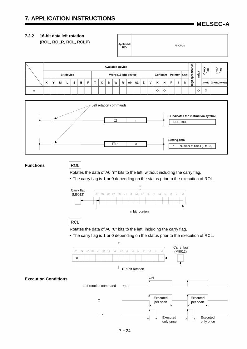
7. APPLICATION INSTRUCTIONS
7 − 24
MELSEC-A
7.2.2 16-bit data left rotation (ROL, ROLR, RCL, RCLP)
Available Device
Bit device Word (16-bit) device Constant Pointer Level Car
ry
flag
Erro
r fla
g
X Y M L S B F T C D W R A0 A1 Z V K H P I N
Digi
t spe
cific
atio
n
Inde
x
M9012 (M9010, M9011)
n O O O O
Functions ROL Rotates the data of A0 "n" bits to the left, without including the carry flag. • The carry flag is 1 or 0 depending on the status prior to the execution of ROL.
RCL Rotates the data of A0 "0" bits to the left, including the carry flag. • The carry flag is 1 or 0 depending on the status prior to the execution of RCL.
Execution Conditions
Applicable CPU All CPUs
Left rotation commands
n
n
ROL, RCL
❏ Indicates the instruction symbol.
n Number of times (0 to 15)
Setting data P
Carry flag (M9012)
n bit rotation
Carry flag (M9012)
n bit rotation
OFF
Executed per scan
Executed per scan
Executed only once
Executed only once
Left rotation command
P
ON

7. APPLICATION INSTRUCTIONS
7 − 25
MELSEC-A
Program Examples ROL Program which rotates the contents of A0 three bits to the left when XC turns on.
RCL Program which rotates the contents of A0 three bits to the left when XC turns on.
Contents of B15 before execution
Contents of B15 when n = 1
Contents of B15 when n = 2
Carry flag (M9012)
To B0
To B0
To B0
(n = 1)
(n = 2)
(n = 3)
Before execution
Progress
After execution
* Before execution, carry flag is either 1 or 0.
X00C P KROL 3 0
• Coding 0 LD X0 1 ROLP K3 4 END
X00C P KRCL 3 0
• Coding 0 LD X00C 1 RCLP K3 4 END
Carry flag (M9012)
* Before execution, carry flag is either 1 or 0.
To carry flag
To carry flag
To carry flag
(n = 1)
(n = 2)
(n = 3) After execution
Progress
Before execution
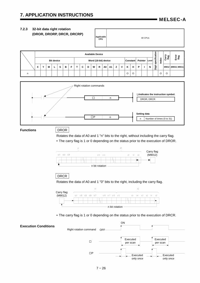
7. APPLICATION INSTRUCTIONS
7 − 26
MELSEC-A
7.2.3 32-bit data right rotation (DROR, DRORP, DRCR, DRCRP)
Available Device
Bit device Word (16-bit) device Constant Pointer Level Car
ry
flag
Erro
r fla
g
X Y M L S B F T C D W R A0 A1 Z V K H P I N
Digi
t spe
cific
atio
n
Inde
x
M9012 (M9010, M9011)
n O O O O
Functions DROR Rotates the data of A0 and 1 "n" bits to the right, without including the carry flag. • The carry flag is 1 or 0 depending on the status prior to the execution of DROR.
DRCR Rotates the data of A0 and 1 "0" bits to the right, including the carry flag.
• The carry flag is 1 or 0 depending on the status prior to the execution of DRCR.
Execution Conditions
Applicable CPU All CPUs
Right rotation commands
n
n
DROR, DRCR
❏ Indicates the instruction symbol.
n Number of times (0 to 31)
Setting data P
OFF
Executed per scan
Executed per scan
Executed only once
Executed only once
Right rotation command
P
ON
Carry flag (M9012)
n bit rotation
Carry flag (M9012)
n bit rotation
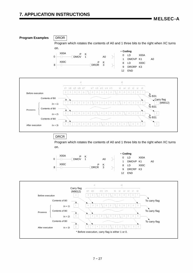
7. APPLICATION INSTRUCTIONS
7 − 27
MELSEC-A
Program Examples DROR Program which rotates the contents of A0 and 1 three bits to the right when XC turns on.
DRCR
Program which rotates the contents of A0 and 1 three bits to the right when XC turns on.
P KDMOV 1 A0
X00A
X00C P KDROR 3
0
8
• Coding 0 LD X00A 1 DMOVP K1 A0 8 LD X00C 9 DRORP K3 12 END
P KDMOV 1 A0
X00A
X00C P KDRCR 3
0
8
• Coding 0 LD X00A 1 DMOVP K1 A0 8 LD X00C 9 DRCRP K3 12 END
Contents of B0
(n = 1)
Contents of B0
(n = 2)
Contents of B0
(n = 3)
Before execution
After execution
Progress
To carry flag
To carry flag
To carry flag
* Before execution, carry flag is either 1 or 0.
Carry flag(M9012)
Contents of B0
(n = 1)
Contents of B0
(n = 2)
Contents of B0
(n = 3)
Before execution
After execution
Progress
To B31
To B31
To B31
Carry flag (M9012)
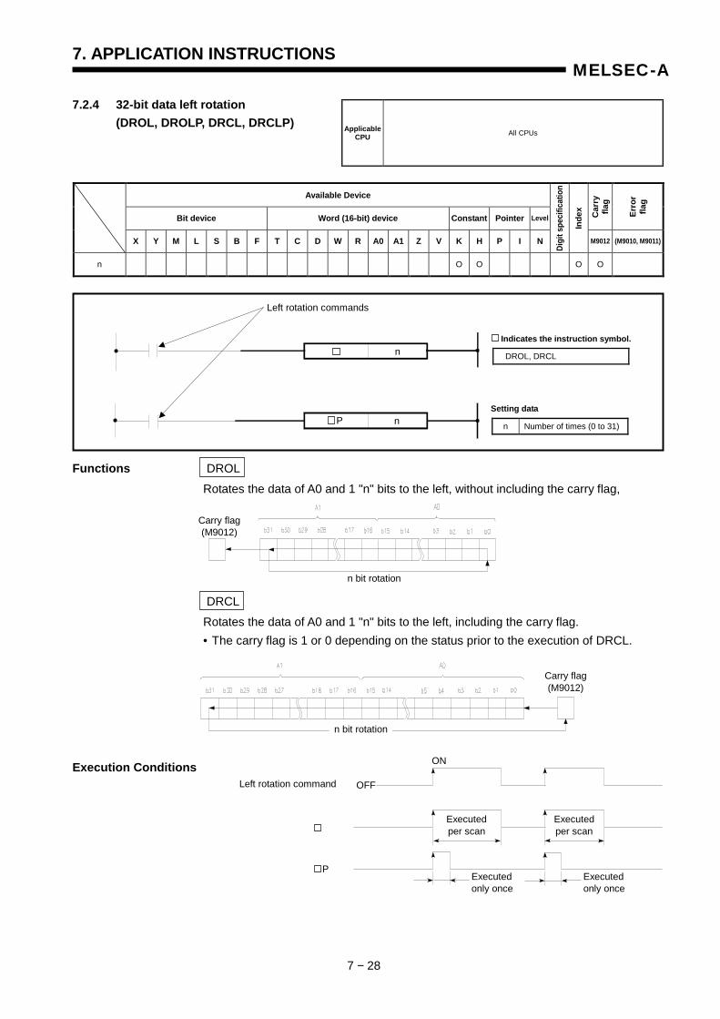
7. APPLICATION INSTRUCTIONS
7 − 28
MELSEC-A
7.2.4 32-bit data left rotation (DROL, DROLP, DRCL, DRCLP)
Available Device
Bit device Word (16-bit) device Constant Pointer Level Car
ry
flag
Erro
r fla
g
X Y M L S B F T C D W R A0 A1 Z V K H P I N
Digi
t spe
cific
atio
n
Inde
x
M9012 (M9010, M9011)
n O O O O
Functions DROL Rotates the data of A0 and 1 "n" bits to the left, without including the carry flag,
DRCL Rotates the data of A0 and 1 "n" bits to the left, including the carry flag. • The carry flag is 1 or 0 depending on the status prior to the execution of DRCL.
Execution Conditions
Applicable CPU All CPUs
Left rotation commands
n
n
DROL, DRCL
Indicates the instruction symbol.
n Number of times (0 to 31)
Setting data P
OFF
Executed per scan
Executed per scan
Executed only once
Executed only once
Left rotation command
P
ON
Carry flag (M9012)
n bit rotation
Carry flag (M9012)
n bit rotation
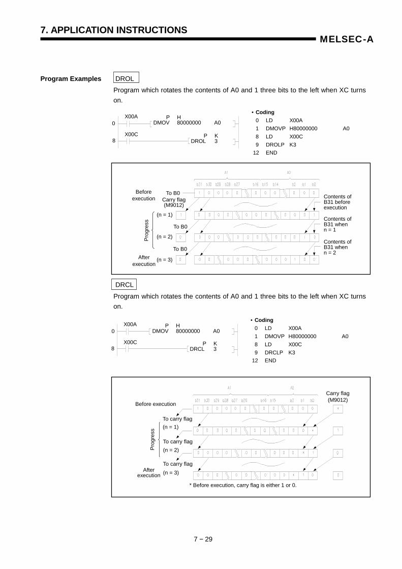
7. APPLICATION INSTRUCTIONS
7 − 29
MELSEC-A
Program Examples DROL Program which rotates the contents of A0 and 1 three bits to the left when XC turns on.
DRCL
Program which rotates the contents of A0 and 1 three bits to the left when XC turns on.
P HDMOV 80000000 A0
X00A
X00C P KDROL 3
0
8
• Coding 0 LD X00A 1 DMOVP H80000000 A0 8 LD X00C 9 DROLP K3 12 END
Carry flag(M9012)
Contents ofB31 beforeexecution
Contents ofB31 when n = 1
Contents ofB31 when n = 2
To B0
(n = 1)
(n = 2)
(n = 3)
To B0
To B0
Prog
ress
Before execution
After execution
P HDMOV 80000000 A0
X00A
X00C P KDRCL 3
0
8
• Coding 0 LD X00A 1 DMOVP H80000000 A0 8 LD X00C 9 DRCLP K3 12 END
* Before execution, carry flag is either 1 or 0.
To carry flag
To carry flag
To carry flag
(n = 1)
(n = 2)
(n = 3)After execution
Before execution
Prog
ress
Carry flag(M9012)
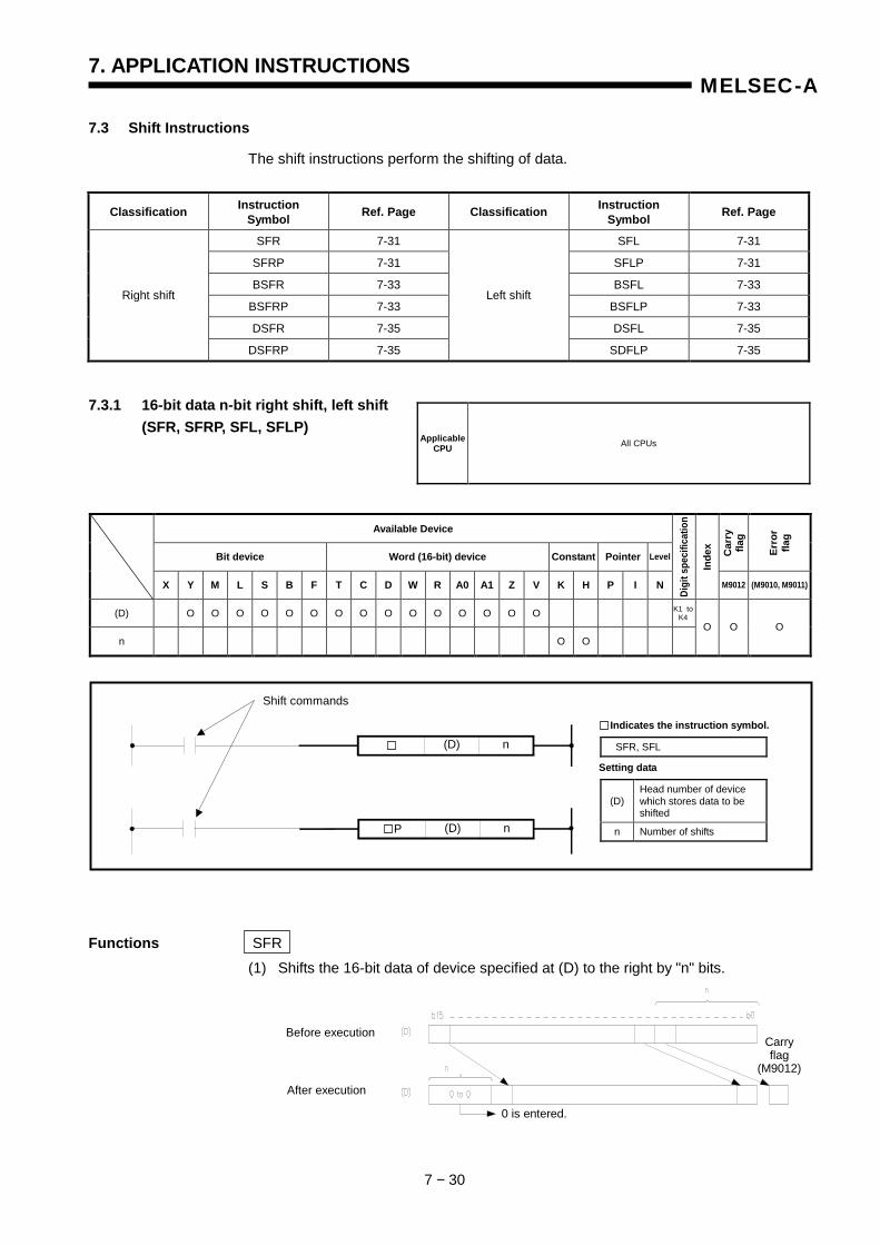
7. APPLICATION INSTRUCTIONS
7 − 30
MELSEC-A
7.3 Shift Instructions
The shift instructions perform the shifting of data.
Classification Instruction Symbol Ref. Page Classification Instruction
Symbol Ref. Page
SFR 7-31 SFL 7-31
SFRP 7-31 SFLP 7-31
BSFR 7-33 BSFL 7-33
BSFRP 7-33 BSFLP 7-33
DSFR 7-35 DSFL 7-35
Right shift
DSFRP 7-35
Left shift
SDFLP 7-35
7.3.1 16-bit data n-bit right shift, left shift (SFR, SFRP, SFL, SFLP)
Available Device
Bit device Word (16-bit) device Constant Pointer Level Car
ry
flag
Erro
r fla
g
X Y M L S B F T C D W R A0 A1 Z V K H P I N
Digi
t spe
cific
atio
n
Inde
x
M9012 (M9010, M9011)
(D) O O O O O O O O O O O O O O O
n O O O O O
Functions SFR (1) Shifts the 16-bit data of device specified at (D) to the right by "n" bits.
Applicable CPU All CPUs
K1 to K4
(D) n
(D) n P
Shift commands
(D) Head number of device which stores data to be shifted
n Number of shifts
Setting data
SFR, SFL
Indicates the instruction symbol.
Carryflag
(M9012)
Before execution
After execution
0 is entered.
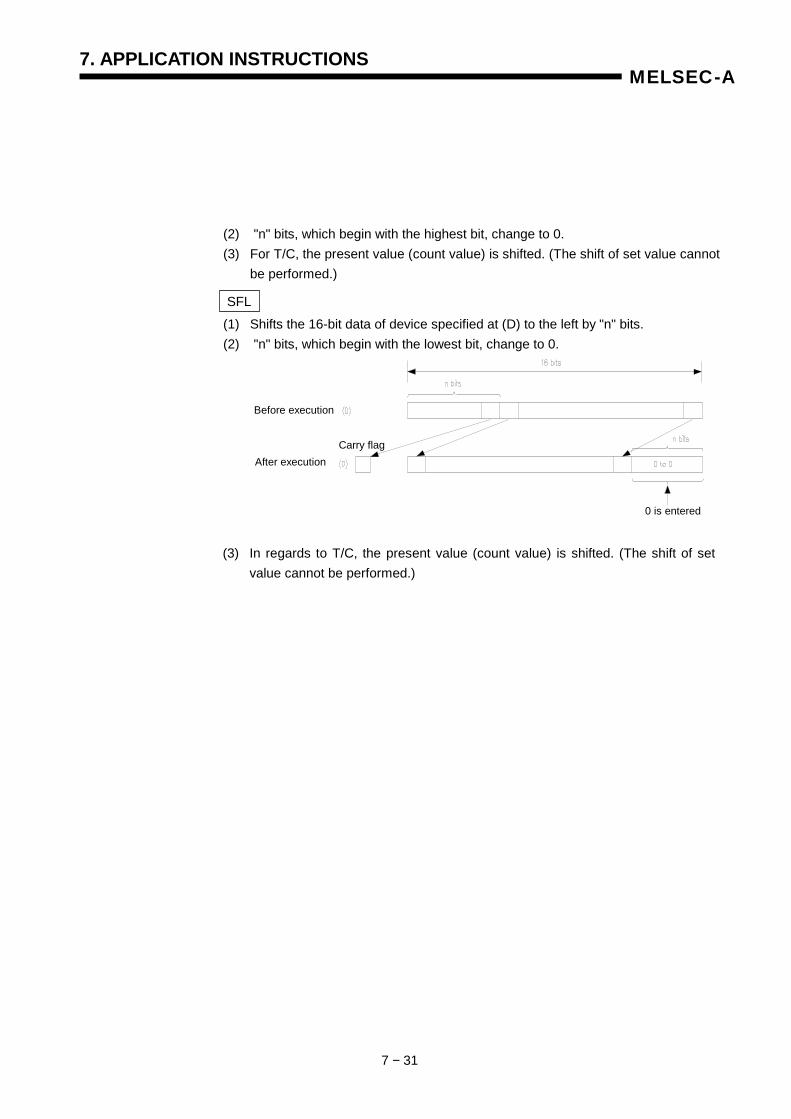
7. APPLICATION INSTRUCTIONS
7 − 31
MELSEC-A
(2) "n" bits, which begin with the highest bit, change to 0. (3) For T/C, the present value (count value) is shifted. (The shift of set value cannot
be performed.)
SFL (1) Shifts the 16-bit data of device specified at (D) to the left by "n" bits. (2) "n" bits, which begin with the lowest bit, change to 0.
Before execution
After execution Carry flag
0 is entered
(3) In regards to T/C, the present value (count value) is shifted. (The shift of set value cannot be performed.)
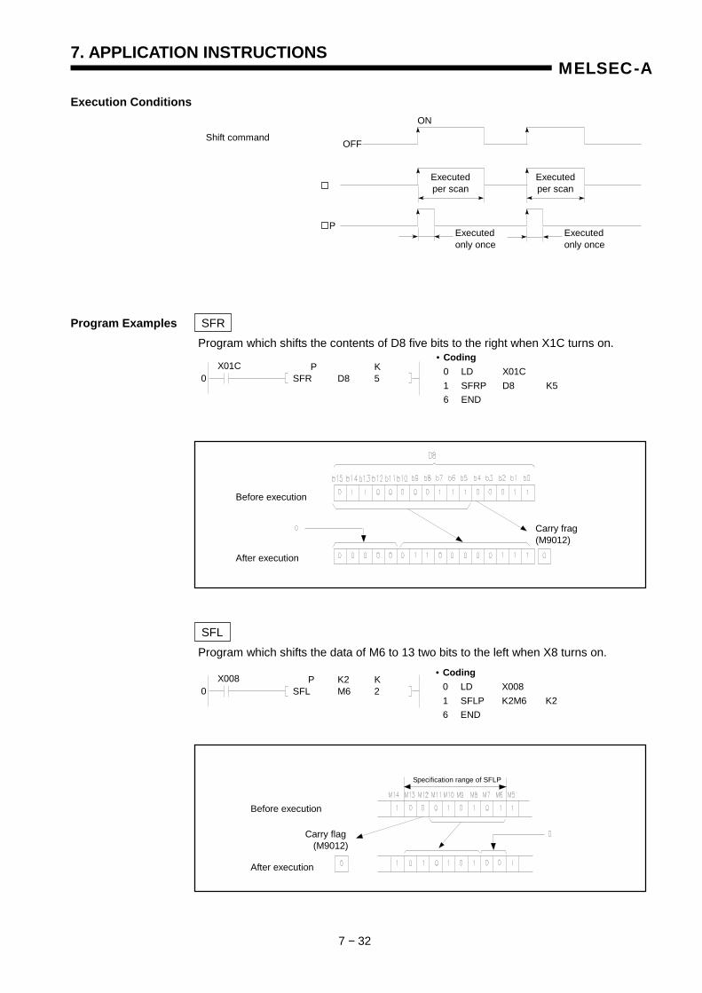
7. APPLICATION INSTRUCTIONS
7 − 32
MELSEC-A
Execution Conditions
Program Examples SFR Program which shifts the contents of D8 five bits to the right when X1C turns on.
SFL Program which shifts the data of M6 to 13 two bits to the left when X8 turns on.
OFF
ON
Executed per scan
Executed per scan
Executed only once
Executed only once
P
Shift command
• Coding 0 LD X01C 1 SFRP D8 K5 6 END
0X01C P K
SFR D8 5
• Coding 0 LD X008 1 SFLP K2M6 K2 6 END
0X008 P K2 K
SFL M6 2
Before execution
After execution
Carry frag (M9012)
Before execution
After execution
Carry flag (M9012)
Specification range of SFLP
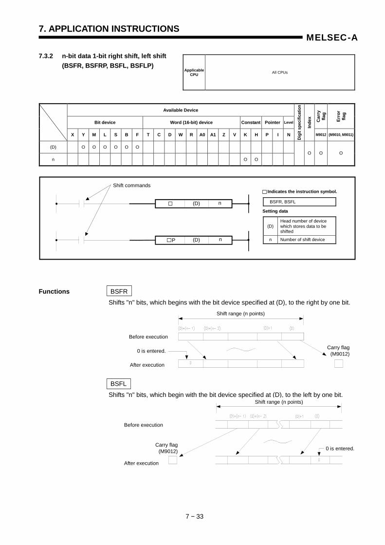
7. APPLICATION INSTRUCTIONS
7 − 33
MELSEC-A
7.3.2 n-bit data 1-bit right shift, left shift (BSFR, BSFRP, BSFL, BSFLP)
Available Device
Bit device Word (16-bit) device Constant Pointer Level Car
ry
flag
Erro
r fla
g
X Y M L S B F T C D W R A0 A1 Z V K H P I N
Digi
t spe
cific
atio
n
Inde
x
M9012 (M9010, M9011)
(D) O O O O O O
n O O O O O
Functions BSFR Shifts "n" bits, which begins with the bit device specified at (D), to the right by one bit.
BSFL
Shifts "n" bits, which begin with the bit device specified at (D), to the left by one bit.
Applicable CPU All CPUs
(D) n
(D) n P
Shift commands
(D) Head number of device which stores data to be shifted
n Number of shift device
Setting data
BSFR, BSFL
Indicates the instruction symbol.
Before execution
After execution
Shift range (n points)
0 is entered. Carry flag (M9012)
Before execution
After execution
Carry flag(M9012) 0 is entered.
Shift range (n points)
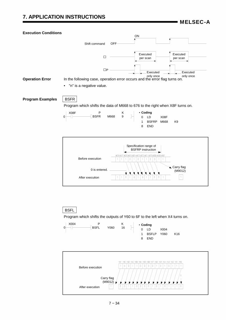
7. APPLICATION INSTRUCTIONS
7 − 34
MELSEC-A
Execution Conditions Operation Error In the following case, operation error occurs and the error flag turns on.
• "n" is a negative value.
Program Examples BSFR Program which shifts the data of M668 to 676 to the right when X8F turns on.
BSFL
Program which shifts the outputs of Y60 to 6F to the left when X4 turns on.
OFF
ON
Executed per scan
Executed per scan
Executed only once
Executed only once
P
Shift command
Specification range ofBSFRP instruction
Before execution
After execution
0 is entered. Carry flag
(M9012)
Before execution
After execution
Carry flag(M9012)
X08F • Coding 0 LD X08F 1 BSFRP M668 K9 8 END
P K BSFR M668 9 0
X004 • Coding 0 LD X004 1 BSFLP Y060 K16 8 END
0 P K BSFL Y060 16
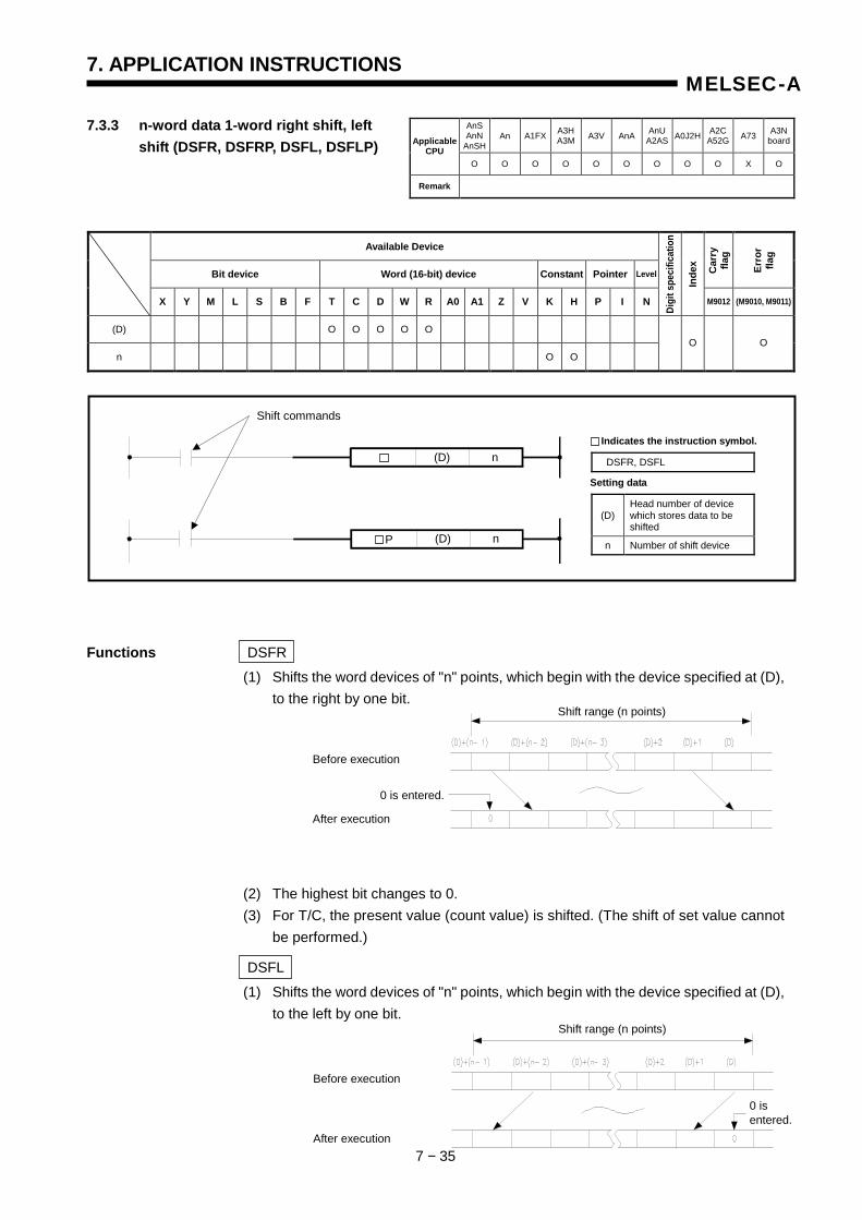
7. APPLICATION INSTRUCTIONS
7 − 35
MELSEC-A
7.3.3 n-word data 1-word right shift, left shift (DSFR, DSFRP, DSFL, DSFLP)
Available Device
Bit device Word (16-bit) device Constant Pointer Level Car
ry
flag
Erro
r fla
g
X Y M L S B F T C D W R A0 A1 Z V K H P I N
Digi
t spe
cific
atio
n
Inde
x
M9012 (M9010, M9011)
(D) O O O O O
n O O O O
Functions DSFR (1) Shifts the word devices of "n" points, which begin with the device specified at (D),
to the right by one bit.
(2) The highest bit changes to 0. (3) For T/C, the present value (count value) is shifted. (The shift of set value cannot
be performed.)
DSFL (1) Shifts the word devices of "n" points, which begin with the device specified at (D),
to the left by one bit.
AnSAnN
AnSHAn A1FX A3H
A3M A3V AnA AnU A2AS A0J2H A2C
A52G A73 A3NboardApplicable
CPU O O O O O O O O O X O
Remark
(D) n
(D) n P
Shift commands
(D) Head number of device which stores data to be shifted
n Number of shift device
Setting data
DSFR, DSFL
Indicates the instruction symbol.
Before execution
After execution
Shift range (n points)
0 is entered.
Before execution
After execution
Shift range (n points)
0 is entered.
7. APPLICATION INSTRUCTIONS
7 − 36
MELSEC-A
(2) The lowest bit changes to 0. (3) In regards to T/C, the present value (count value) is shifted.
(The shift of set value cannot be performed.) Execution Conditions
Operation Error In the following case, operation error occurs and the error flag turns on. • "n" is a negative value.
Program Examples DSFR Program which shifts the contents of D683 to 689 to the right when XB turns on.
DSFL Program which shifts the contents of D683 to 689 to the left when XB turns on.
OFF
ON
Executed per scan
Executed per scan
Executed only once
Executed only once
P
Shift command
• Coding 0 LD X00B 1 DSFRP D683 K7 8 END
0 X00B P K
DSFR D683 7
0 X00B • Coding
0 LD X00B 1 DSFLP D683 K7 8 END
P K DSFL D683 7
Before execution
After execution
Specification range of DSFRP instruction
Before execution
After execution
Specification range of DSFRP instruction
7. APPLICATION INSTRUCTIONS
7 − 37
MELSEC-A
7.4 Data Processing Instructions
The data processing instructions perform operations such as the search, decode, and encode of data.
Classification Instruction Symbol Ref. Page
SER 7-38 Search
SERP 7-38
SUM 7-40
SUMP 7-40
DSUM 7-40 Bit check
DSUMP 7-40
DECO 7-42
DECOP 7-42
ENCO 7-42 Decode Encode
ENCOP 7-42
7 segment decode SEG 7-44
BSET 7-46
BSETP 7-46
BRST 7-46
Bit set
reset BRSTP 7-46
DIS 7-48
DISP 7-48
UNI 7-48 16-bit data
association/dissociation
UNIP 7-48
ASCII conversion ASC 7-51
7. APPLICATION INSTRUCTIONS
7 − 38
MELSEC-A
7.4.1 16-bit data search (SER, SERP)
Available Device
Bit device Word (16-bit) device Constant Pointer Level Car
ry
flag
Erro
r fla
g
X Y M L S B F T C D W R A0 A1 Z V K H P I N
Digi
t spe
cific
atio
n
Inde
x
M9012 (M9010, M9011)
(S1) O O O O O O O O O O O
(S2) O O O O O
n O O
O O
Functions (1) Searches the data of "n" points, beginning with the 16-bit data of device specified at (S2), by use of the 16-bit data of device specified at (S1) as a keyword.
(2) Stores to A1 the number of data which have coincided with the keyword, and
stores to A0 at which point from (S2) the first coinciding device number (relative value) is located.
(3) When "n" is negative, it is equal to 0. (4) When "n" is 0, no processing is performed.
Execution Conditions
Applicable CPU All CPUs
(S1) Device number which stores data to be searched
(S2) Head number of device to be searched
n Number of devices to be searched
Setting data Search commands
SER (S1) (S2) n
SERP (S1) (S2) n
OFF
ON
Executed per scan
Executed per scan
Executed only once
Executed only once
Search command
SER
SERP
7. APPLICATION INSTRUCTIONS
7 − 39
MELSEC-A
Operation Error In the following case, operation error occurs and the error flag turns on.
• When "n" points are searched beginning with (S2), the specified device range is exceeded.
Program Example SER Program which compares the data of D883 to 887 with 123 when XB turns on.
X00B 0
P K KSER 123 D883 5
• Coding 0 LD X00B 1 SERP K123 D883 K5 10 END
Searched data
1 2 3
3
Head number to be searched
D882
D883
D884
D885
D886
D887
D888
1 2 3
1 0
5 0 0
1 2 3
2 0
1 2 3
1 2 3
Coinciding data
Search range (5 pcs.)
2
A0
A1
Search result
A0: Coinciding position A1: Number of coincidences
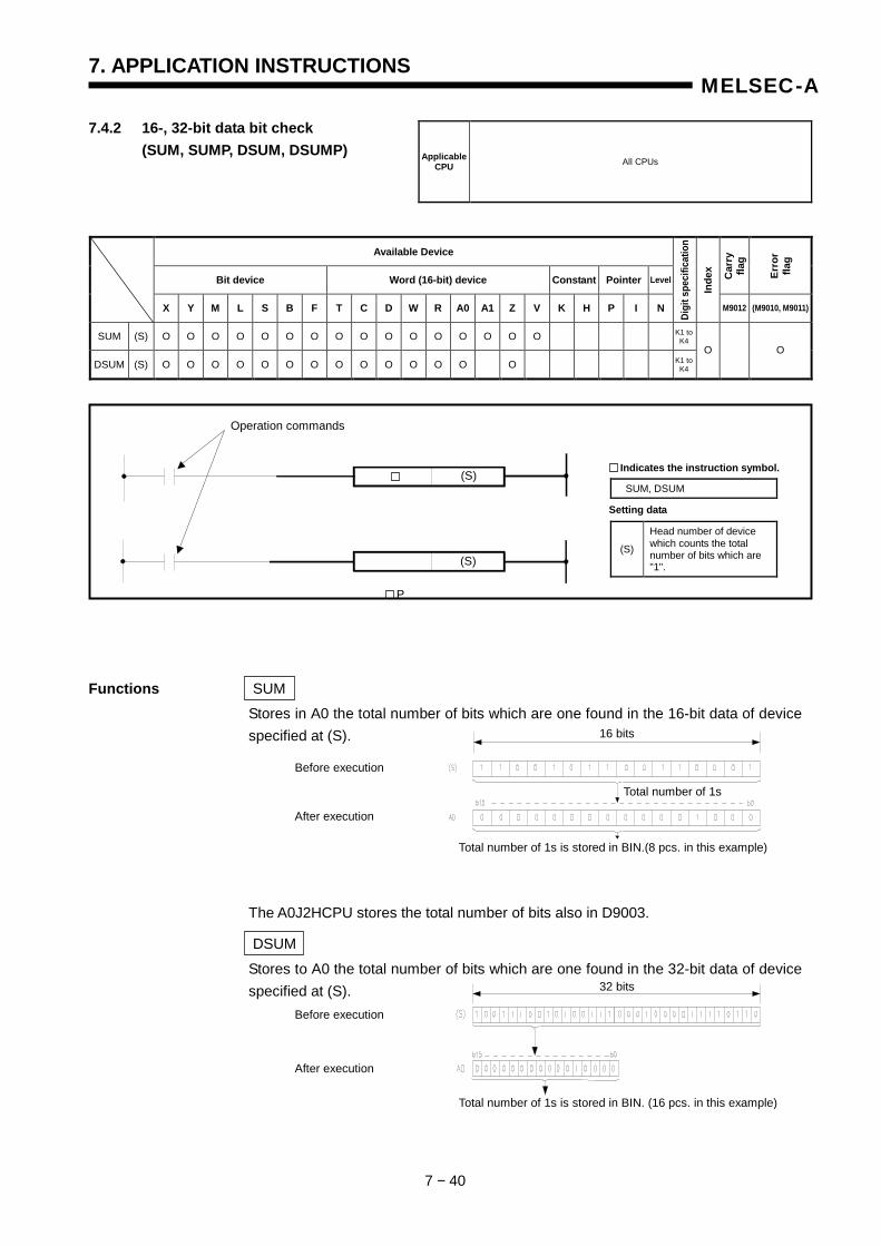
7. APPLICATION INSTRUCTIONS
7 − 40
MELSEC-A
7.4.2 16-, 32-bit data bit check (SUM, SUMP, DSUM, DSUMP)
Available Device
Bit device Word (16-bit) device Constant Pointer Level Car
ry
flag
Erro
r fla
g
X Y M L S B F T C D W R A0 A1 Z V K H P I N
Digi
t spe
cific
atio
n
Inde
x
M9012 (M9010, M9011)
SUM (S) O O O O O O O O O O O O O O O O
DSUM (S) O O O O O O O O O O O O O O O O
Functions SUM Stores in A0 the total number of bits which are one found in the 16-bit data of device specified at (S).
The A0J2HCPU stores the total number of bits also in D9003.
DSUM Stores to A0 the total number of bits which are one found in the 32-bit data of device specified at (S).
Applicable CPU All CPUs
K1 to K4
K1 to K4
Operation commands
(S)
Head number of device which counts the total number of bits which are "1".
Setting data
SUM, DSUM
Indicates the instruction symbol. (S)
(S)
P
Before execution
After execution
Total number of 1s
Total number of 1s is stored in BIN.(8 pcs. in this example)
16 bits
Before execution
After execution
Total number of 1s is stored in BIN. (16 pcs. in this example)
32 bits
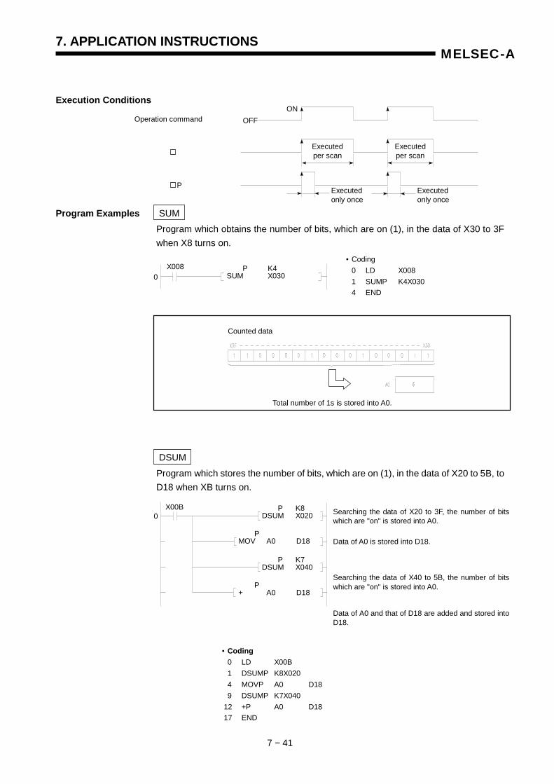
7. APPLICATION INSTRUCTIONS
7 − 41
MELSEC-A
Execution Conditions Program Examples SUM
Program which obtains the number of bits, which are on (1), in the data of X30 to 3F when X8 turns on.
DSUM
Program which stores the number of bits, which are on (1), in the data of X20 to 5B, to D18 when XB turns on.
OFF ON
Executed per scan
Executed per scan
Executed only once
Executed only once
Operation command
P
• Coding 0 LD X008 1 SUMP K4X030 4 END
X008 0
P K4SUM X030
Counted data
Total number of 1s is stored into A0.
Searching the data of X20 to 3F, the number of bits which are "on" is stored into A0.
X00B 0
P K8DSUM X020
P K7DSUM X040
PMOV A0 D18
P+ A0 D18
Data of A0 is stored into D18.
Searching the data of X40 to 5B, the number of bits which are "on" is stored into A0.
Data of A0 and that of D18 are added and stored into D18.
• Coding 0 LD X00B 1 DSUMP K8X020 4 MOVP A0 D18 9 DSUMP K7X040 12 +P A0 D18 17 END
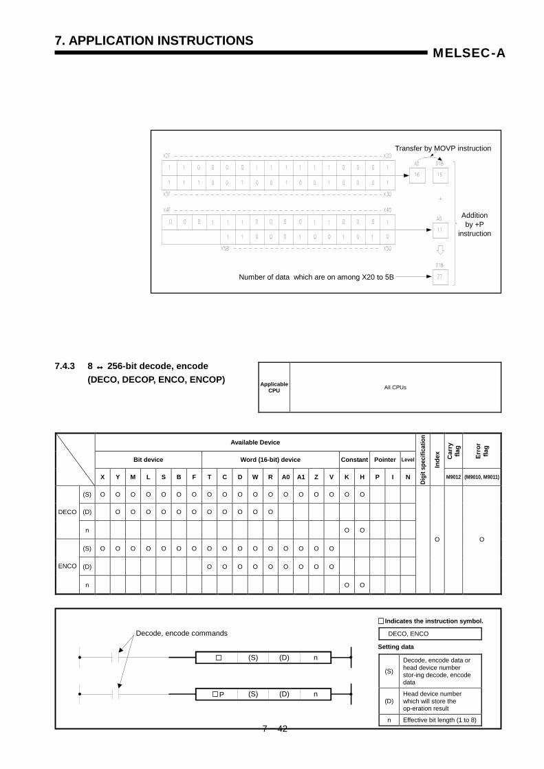
7. APPLICATION INSTRUCTIONS
7 − 42
MELSEC-A
7.4.3 8 ↔↔↔↔ 256-bit decode, encode
(DECO, DECOP, ENCO, ENCOP)
Available Device
Bit device Word (16-bit) device Constant Pointer Level Car
ry
flag
Erro
r fla
g
X Y M L S B F T C D W R A0 A1 Z V K H P I N
Digi
t spe
cific
atio
n
Inde
x
M9012 (M9010, M9011)
(S) O O O O O O O O O O O O O O O O O O
(D) O O O O O O O O O O O DECO
n O O
(S) O O O O O O O O O O O O O O O O
(D) O O O O O O O O O ENCO
n O O
O O
Transfer by MOVP instruction
Addition by +P
instruction
Number of data which are on among X20 to 5B
Applicable CPU All CPUs
(S)
Decode, encode data or head device number stor-ing decode, encode data
(D) Head device number which will store the op-eration result
n Effective bit length (1 to 8)
Setting data
DECO, ENCO
Indicates the instruction symbol.
P
(S) (D) n
(S) (D) n
Decode, encode commands
7. APPLICATION INSTRUCTIONS
7 − 43
MELSEC-A
Functions DECO
8 → 256 bit decode (1) Decodes the lower "n" bits of device specified at (S) and stores the result of
decode data to 2n bits which begin with the device specified at (D). (2) For "n", 1 to 8 can be specified. (3) When "n" is 0, no processing is performed and the contents of 2n bits, which
begin with the device specified at (D), do not change. (4) A bit device is treated as one bit and a word device as 16 bits.
ENCO
256 → 8 bit decode (1) Encodes the data of 2n bits, which begin with (S), and stores the result to (D). (2) For "n", 0 to 8 can be specified. (3) When "n" is 0, no processing is performed and the contents of (D) do not change. (4) The bit device is treated as one bit and the word device as 16 bits. (5) When multiple bits are 1, processing is performed for the last bit position.

7. APPLICATION INSTRUCTIONS
7 − 44
MELSEC-A
Execution Conditions
Operation Errors In the following case, operation error occurs and the error flag turns on.
• "n" in other than 0 to 8. • 0 exists in all devices from S to 2n when the encode instruction is used.
Program Examples DECO
ENCO
OFF ON
Executed per scan
Executed per scan
Executed only once
Executed only once
Decode Encode command
P
M0 0
P KDECO X000 M10 3
• Coding 0 LD M0 1 DECOP X000 M10 K3 10 END
When 3 is specified atX0 to 2
When 8 is specified at effective bits, 256 points are occupied.
Decode result
When 3 is specified as effective bits, 8 points are occupied.
Data
M13 at the third position from M10 turns on.
X00C 0
P KENCO M10 D8 3
CIRCUIT END
• Coding 0 LD X00C 1 ENCOP M10 D8 K3 10 END
When 8 is specified as effective bits, 256 points are occupied.
When 3 is specified as effective bits, 8 points are occupied.
Device D8 Encode result
Which point, counting from M10, is on is stored in BIN.
7. APPLICATION INSTRUCTIONS
7 − 44
MELSEC-A
7.4.4 7 segment decode (SEG)
The SEG instruction for the CPUs except An changes in function depending on the status of special relay M9052, as follows. When M9052 is ON: Partial refresh (See Section 6.7.3 for details.) When M9052 is OFF: 7-segment decode
Available Device
Bit device Word (16-bit) device Constant Pointer Level Car
ry
flag
Erro
r fla
g
X Y M L S B F T C D W R A0 A1 Z V K H P I N
Digi
t spe
cific
atio
n
Inde
x
M9012 (M9010, M9011)
(S) O O O O O O O O O O O O O O O O O O K1
(D) O O O O O O O O O O O O O O O O
*1: If the CPUs other than A3H, A3M, AnA, A2AS, and AnU are used, digit specification is ignored and 8-bit (2 digits) data is always output.
Functions (1) Decodes the data of 0 to F specified at the lower four bits of (S) to seven- segment display data and stores the result to (D).
(2) When the device is a bit device (Y, M, L, S, B, F), indicates the head number of
device which will store the seven-segment display data. When the device is a word device (T, C, D, R, A0, A1, Z, V), indicates the device number which will store the seven-segment display data.
(3) The data is stored into the bit device and word device as shown below.
AnSAnN
AnSHAn A1FX A3H
A3M A3V AnA AnU A2AS A0J2H A2C
A52G A73 A3Nboad Applicable
CPU O X
Remark * Valid only when special relay M9052 is OFF.
* * * * * * * * *
K1 to*1 K4
Decode command Not necessary for the An.
(S) (D)
M9052RST
SEG
(S)
Data to be decoded or head number of device which stores data to be decoded
(D) Head number of device which will store decode result.
Setting data
Before execution
Bit device
After execution
Word device
8 points
Upper 8 bits are set to 0. 7-segment display data is stored into lower 8 bits.
D8

7. APPLICATION INSTRUCTIONS
7 − 45
MELSEC-A
(4) For the seven-segment display data, refer to the next page.
Execution Conditions
(S) (D)
Hexadecimal number Bit pattern
Configuration of 7-segment B7 B6 B5 B4 B3 B2 B1 B0
Displayed Data
0 0000 0 0 1 1 1 1 1 1
1 0001 0 0 0 0 0 1 1 0
2 0010 0 1 0 1 1 0 1 1
3 0011 0 1 0 0 1 1 1 1
4 0100 0 1 1 0 0 1 1 0
5 0101 0 1 1 0 1 1 0 1
6 0110 0 1 1 1 1 1 0 1
7 0111 0 0 1 0 0 1 1 1
8 1000 0 1 1 1 1 1 1 1
9 1001 0 1 1 0 1 1 1 1
A 1010 0 1 1 1 0 1 1 1
B 1011 0 1 1 1 1 1 0 0
C 1100 0 0 1 1 1 0 0 1
D 1101 0 1 0 1 1 1 1 0
E 1110 0 1 1 1 1 0 0 1
F 1111
0 1 1 1 0 0 0 1
OFF
ON
Executed per scan
Executed per scan
Decode command
SEG
B0
B6
B3
B5 B1
B4 B2
Head of bit device The lowest bit of word device
7. APPLICATION INSTRUCTIONS
7 − 46
MELSEC-A
Program Example SEG Program which converts the data of XC to F to seven-segment display data and sends the display data to Y38 to 3F when X0 turns on.
X0
Y38 to 3F
*Y38 to 3F do not change until the next data is output.
• Coding 0 LD X000 1 SEG K1X00C K2Y038 8 END
X000 0
K1 K2SEG X00C Y038
7. APPLICATION INSTRUCTIONS
7 − 46
MELSEC-A
7.4.5 Word device bit set, reset (BSET, BSETP, BRST, BRSTP)
Available Device
Bit device Word (16-bit) device Constant Pointer Level Car
ry
flag
Erro
r fla
g
X Y M L S B F T C D W R A0 A1 Z V K H P I N
Digi
t spe
cific
atio
n
Inde
x
M9012 (M9010, M9011)
(D) O O O O O O O O O
n O O O O
Functions BSET (1) Sets (1) the "n"th bit of word device specified at (D). (2) For "n", 0 to 15 are effective. When 15 is exceeded, the instruction is executed at
the lower four bits.
BRST
(1) Resets (0) the "n"th bit of word device specified at (D). (2) For "n", 0 to 15 are effective. When 15 is exceeded, the instruction is executed at
Applicable CPU All CPUs
(D) Device number for bit set, reset
n Bit number for bit set, reset
Setting data
BSET, BRST
Indicates the instruction symbol.
Set/reset commands
P
(D) n
(D) n
Before execution
After execution
Set to 1.
P KBSET D10 6
P KBRST D10 11
7. APPLICATION INSTRUCTIONS
7 − 47
MELSEC-A
the lower four bits. Execution Conditions
Program Example BEST , BRST Program which sets the 3rd bit and 8th bit of D19 when X18 turns on.
OFF ON
Executed per scan
Executed per scan
Executed only once
Executed only once
Set Reset command
P
• Coding 0 LDI X00B 1 BRSTP D8 K8 8 LD X00B 9 BSETP D8 K3 16 END
Before execution
After execution
When XB turns off When XB turns on
Before execution
After execution
Set to 0.
The 8th bit of D8 is reset.
The 3rd bit of D8 is set.
X00B
X00B
0
8
P KBRST D8 8
P KBSET D8 3
7. APPLICATION INSTRUCTIONS
7 − 48
MELSEC-A
7.4.6 16-bit data dissociation, association (DIS, DISP, UNI, UNIP)
Available Device
Bit device Word (16-bit) device Constant Pointer Level Car
ry
flag
Erro
r fla
g
X Y M L S B F T C D W R A0 A1 Z V K H P I N
Digi
t spe
cific
atio
n
Inde
x
M9012 (M9010, M9011)
(S) O O O O O O O O O O O
(D) O O O O O DIS
n O O
(S) O O O O O
(D) O O O O O O O O O UNI
n O O
O O
Functions DIS (1) Stores the data of lower "n" digits (one digit consists of four bits) of 16-bit data
specified at (S) into the lower four bits of devices of "n" points which begin with the device specified at (D).
(S) Head device number stor-ing data to be dissociated, associated
(D) Device number which will store data dissociated, associated
n
• Number of devices for dissociation(1 to 4) • Number of data associ- ated (1 to 4)
Setting data
DIS, UNI
Indicates the instruction symbol.
Applicable CPU All CPUs
K1 to K4
Dissociation/association commands
P
(D) n
(D) n
(S)
(S)
Before execution
Set to 0. Storage area
After execution
7. APPLICATION INSTRUCTIONS
7 − 49
MELSEC-A
(2) The upper 12 bits of devices of "n" points, which begin with the device specified at
(D), are set to 0.
(3) For "n", 1 to 4 can be specified.
(4) When "n" is 0, no processing is performed and the contents of "n" points beginning with the device of (D) do not change.
UNI (1) Associates the data of lower four bits of 16-bit data in devices of "n" points, which
begin with the device specified at (S), to the 16-bit device specified at (D).
(2) The bits of upper (4 - n)-digits of device specified at (D), are set to 0. (3) For "n", 1 to 4 can be specified. (4) When "n" is 0, no processing is performed and the contents of device of (D) do
not change.
Execution Conditions
Operation Error In the following case, operation error occurs and the error flag turns on. • "n" is other than 0 to 4.
OFF
ON
Executed per scan
Executed per scan
Executed only once
Executed only once
Dissociation/association commands
P
Before execution After execution
Ignored Data to be associated
7. APPLICATION INSTRUCTIONS
7 − 50
MELSEC-A
Program Examples DIS Program which stores the 16-bit data of D0 to the D10 to 13 per four bits when X0 turns on.
UNI
Program which stores the lower four-bit data of D0 to 2 to the D10 when X0 turns on.
X000 0
P KDIS D0 D10 4
• Coding 0 LD X000 1 DISP D0 D10 K4 10 END
Before execution After execution
Set to 0. Storage area
X000 0
P KUNI D0 D10 3
• Coding 0 LD X000 1 UNIP D0 D10 K3 10 END
Before execution After execution
Data to be associated
7. APPLICATION INSTRUCTIONS
7 − 51
MELSEC-A
7.4.7 ASCII code conversion (ASC)
Available Device
Bit device Word (16-bit) device Constant Pointer Level Car
ry
flag
Erro
r fla
g
X Y M L S B F T C D W R A0 A1 Z V K H P I N
Digi
t spe
cific
atio
n
Inde
x
M9012 (M9010, M9011)
(D) O O O O O O O
Function Converts the specified alphanumeric characters into the ASCII code and stores the result into devices of four points which begin with the device specified at (D).
Executed Conditions
Applicable CPU All CPUs
(D) Head number of device which will store ASCII code
Setting data
Conversion command
(D)ASC ASCII characters(8 characters)
Before execution
Conversion into ASCII code
After execution
Lower 8 bits
Upper 8 bits
ASCII code to be stored (hexadecimal)
OFF
ON
Conversion command
ASC Executed only once
Executed only once
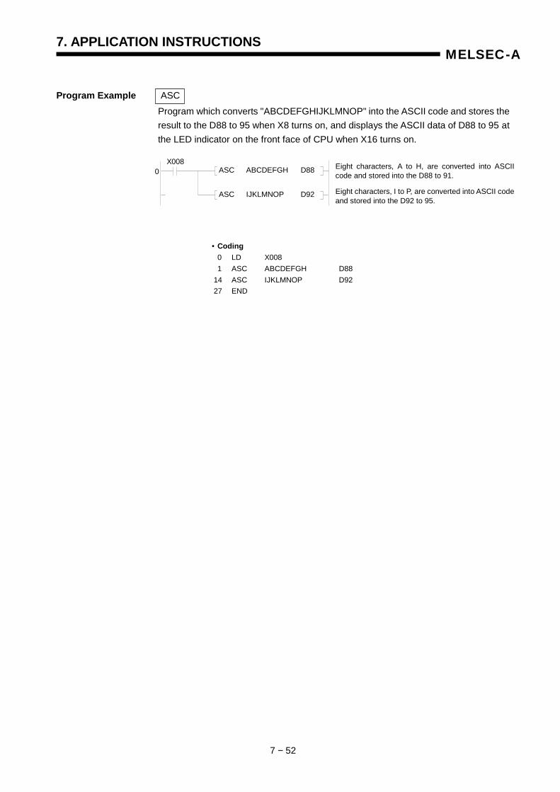
7. APPLICATION INSTRUCTIONS
7 − 52
MELSEC-A
Program Example ASC
Program which converts "ABCDEFGHIJKLMNOP" into the ASCII code and stores the result to the D88 to 95 when X8 turns on, and displays the ASCII data of D88 to 95 at the LED indicator on the front face of CPU when X16 turns on.
X008 0 ASC ABCDEFGH D88
ASC IJKLMNOP D92
Eight characters, A to H, are converted into ASCII code and stored into the D88 to 91.
Eight characters, I to P, are converted into ASCII code and stored into the D92 to 95.
• Coding 0 LD X008 1 ASC ABCDEFGH D88 14 ASC IJKLMNOP D92 27 END

7. APPLICATION INSTRUCTIONS
7 − 53
MELSEC-A
7.5 FIFO Instructions
The FIFO instructions perform the write and read of data to and from the FIFO table.
Classification Instruction Symbol Ref. Page
FIFW 7-54 Write
FIFWP 7-54
FIFR 7-54 Read
FIFRP 7-54

7. APPLICATION INSTRUCTIONS
7 − 54
MELSEC-A
7.5.1 FIFO table write, read (FIFW, FIFWP, FIFR, FIFRP)
Available Device
Bit device Word (16-bit) device Constant Pointer Level Car
ry
flag
Erro
r fla
g
X Y M L S B F T C D W R A0 A1 Z V K H P I N
Digi
t spe
cific
atio
n
Inde
x
M9012 (M9010, M9011)
(S) O O O O O O O O O O O O O O O O O O FIFW
(D) O O O O O
(S) O O O O O O O O O O O O O O O FIFR
(D) O O O O O
O O
Functions FIFW (1) Performs the following actions:
1) Stores the data specified at (S) into the data table of FIFO table. The storage position of data is as indicated below.
Data storage position = head address of data table + content of pointer
2) Adds 1 to the content of pointer. (For the pointer, use the device specified at (D).)
(2) To use the FIFW instruction for the first time, clear the pointer specified at (D) before executing the instruction.
Applicable CPU All CPUs
K1 to K4
K1 to K4
(3) To perform the management of the number of data which may be written to multiple FIFO tables, use the user program.
Read commands Indicates the instruction symbol.
(S)
• Data to be written to FIFO table or head number of device which stores data • Device number which will store data read
(D) Head device number of FIFO table
Setting data
FIFW, FIFR
(S) (D)
(D) (S) P
Pointer The number of data stored in data table is stored.
Head of FIFO table
Device number of destination
(D)+0 (D)+1 (D)+2
Data table Data written by FIFW or FIFWP in-struction is stored.
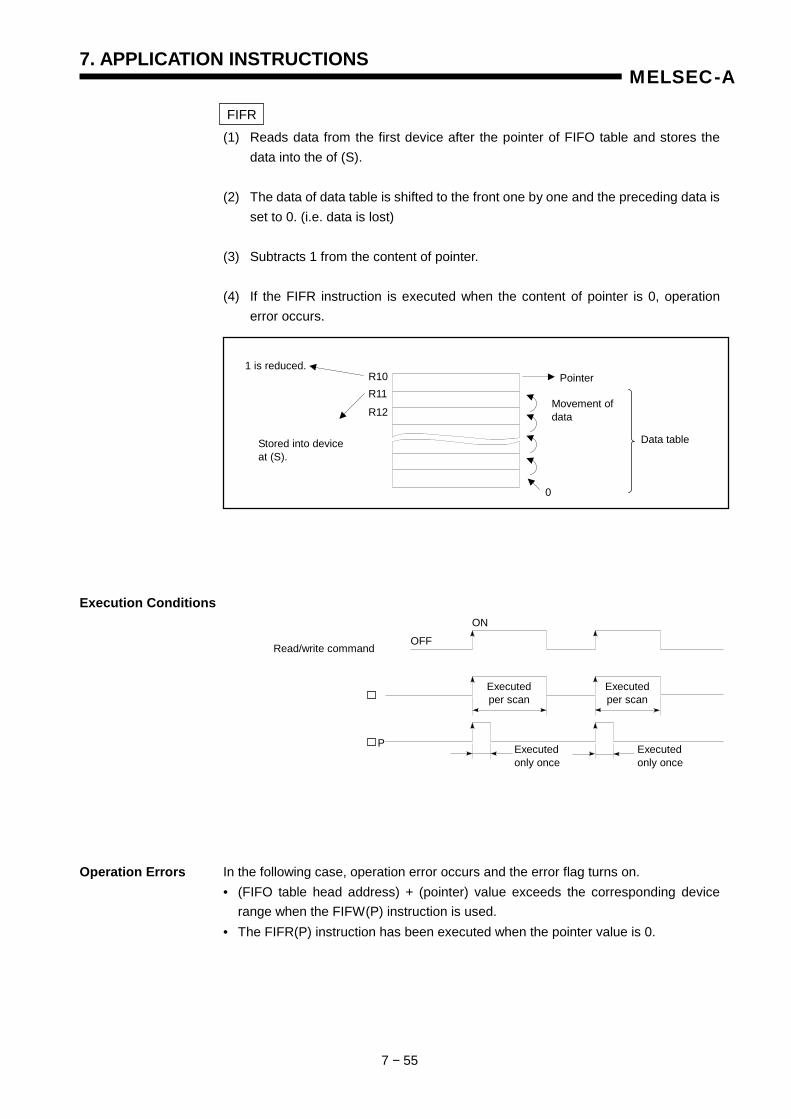
7. APPLICATION INSTRUCTIONS
7 − 55
MELSEC-A
FIFR (1) Reads data from the first device after the pointer of FIFO table and stores the
data into the of (S). (2) The data of data table is shifted to the front one by one and the preceding data is
set to 0. (i.e. data is lost) (3) Subtracts 1 from the content of pointer. (4) If the FIFR instruction is executed when the content of pointer is 0, operation
error occurs.
Execution Conditions
Operation Errors In the following case, operation error occurs and the error flag turns on. • (FIFO table head address) + (pointer) value exceeds the corresponding device range when the FIFW(P) instruction is used. • The FIFR(P) instruction has been executed when the pointer value is 0.
OFF
ON
Executed per scan
Executed per scan
Executed only once
Executed only once
Read/write command
P
Stored into device at (S).
1 is reduced. R10 R11
R12
0
Data table
Pointer
Movement of data
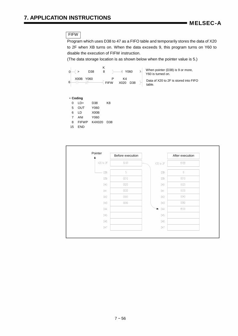
7. APPLICATION INSTRUCTIONS
7 − 56
MELSEC-A
FIFW Program which uses D38 to 47 as a FIFO table and temporarily stores the data of X20 to 2F when XB turns on. When the data exceeds 9, this program turns on Y60 to disable the execution of FIFW instruction. (The data storage location is as shown below when the pointer value is 5.)
• Coding 0 LD> D38 K8 5 OUT Y060 6 LD X00B 7 ANI Y060 8 FIFWP K4X020 D38 15 END
PointerBefore execution After execution
Data of X20 to 2F is stored into FIFO table.
When pointer (D38) is 9 or more, Y60 is turned on.
( )0
6
K > D38 8 Y060
X00B Y060 P K4 FIFW X020 D38

7. APPLICATION INSTRUCTIONS
7 − 57
MELSEC-A
FIFR Program which reads data from D38 to 45 of the FIFO table when XB turns on, and outputs the data to the Y30 to 3F. (Data is read as shown below when the pointer value is 7.)
• Coding 0 LD= K0 D38 5 OUT Y060 6 LD X00B 7 ANI Y060 8 FIFRP K4Y030 D38 15 END
Pointer
Before execution After execution
K = 0 D38 Y060 When pointer (D38) is 0, Y60 is turns
on.
Data is read from FIFO table and output to Y30 to 3F.
( )0
6 P K4 FIFR Y030 D38
X00B Y060

7. APPLICATION INSTRUCTIONS
7 − 58
MELSEC-A
7.6 Buffer Memory Access Instructions
Buffer memory access instructions are used to read and write data of buffer memory of special function modules and remote terminal modules (when the A2C, A52G is used). There are 16 types of buffer memory access instructions as shown below.
Classification Instruction Symbol Ref. Page
FROM 7-59
FROMP 7-59
DFRO 7-59 Special function
module data read
DFROP 7-59
TO 7-61
TOP 7-61
DTO 7-61 Special function
module data write
DTOP 7-61
FROM, PRC 7-63
FROMP, PRC 7-63
DFRO, PRC 7-63 Remote terminal
data read
DFROP, PRC 7-63
TO, PRC 7-67
TOP, PRC 7-67
DTO, PRC 7-67 Remote terminal
data write
DTOP, PRC 7-67
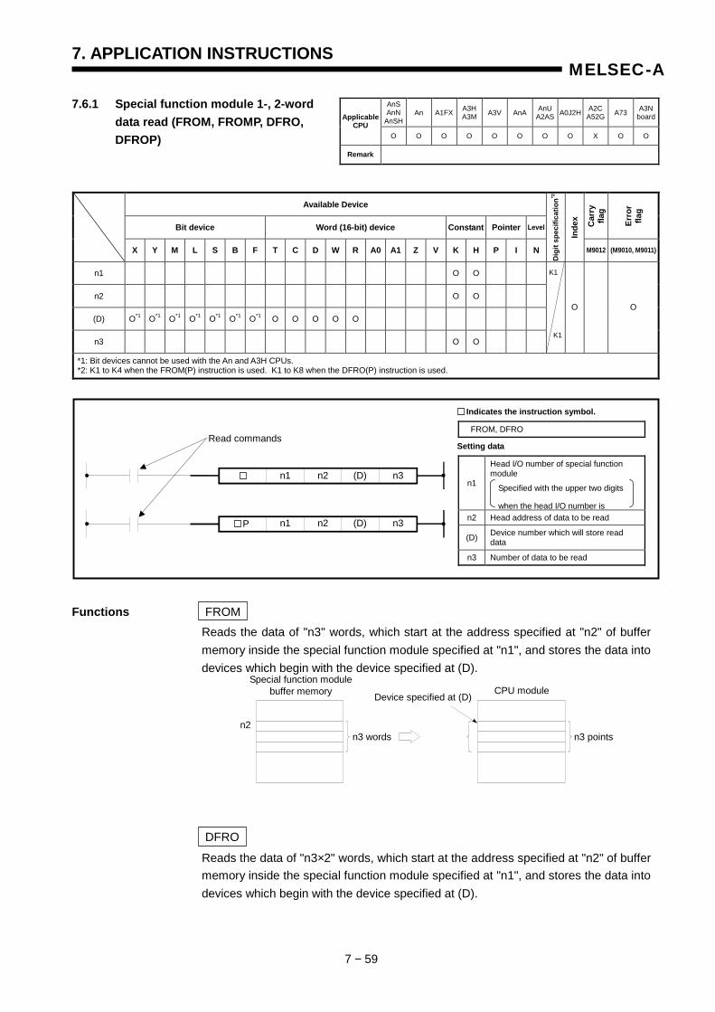
7. APPLICATION INSTRUCTIONS
7 − 59
MELSEC-A
7.6.1 Special function module 1-, 2-word data read (FROM, FROMP, DFRO, DFROP)
Available Device
Bit device Word (16-bit) device Constant Pointer Level Car
ry
flag
Erro
r fla
g
X Y M L S B F T C D W R A0 A1 Z V K H P I N
Dig
it sp
ecifi
catio
n*2
Inde
x
M9012 (M9010, M9011)
n1 O O
n2 O O
(D) O*1 O*1 O*1 O*1 O*1 O*1 O*1 O O O O O
n3 O O
O O
*1: Bit devices cannot be used with the An and A3H CPUs. *2: K1 to K4 when the FROM(P) instruction is used. K1 to K8 when the DFRO(P) instruction is used.
Functions FROM Reads the data of "n3" words, which start at the address specified at "n2" of buffer memory inside the special function module specified at "n1", and stores the data into devices which begin with the device specified at (D).
DFRO
Reads the data of "n3×2" words, which start at the address specified at "n2" of buffer memory inside the special function module specified at "n1", and stores the data into devices which begin with the device specified at (D).
AnSAnN
AnSHAn A1FX A3H
A3M A3V AnA AnU A2AS A0J2H A2C
A52G A73 A3NboardApplicable
CPU O O O O O O O O X O O
Remark
Special function module buffer memory CPU module
n2
Device specified at (D)
n3 pointsn3 words
K1
t
K1
t
n3
n3
n1
Head I/O number of special function module
n2 Head address of data to be read
(D) Device number which will store read data
n3 Number of data to be read
Setting data
FROM, DFRO
Indicates the instruction symbol.
n1 (D)
n1 (D)P
n2
n2
Read commands
Specified with the upper two digits
when the head I/O number is

7. APPLICATION INSTRUCTIONS
7 − 60
MELSEC-A
Special function module buffer memory CPU module
n2
Device specified at (D)
(n3×2) points
(n3×2) words
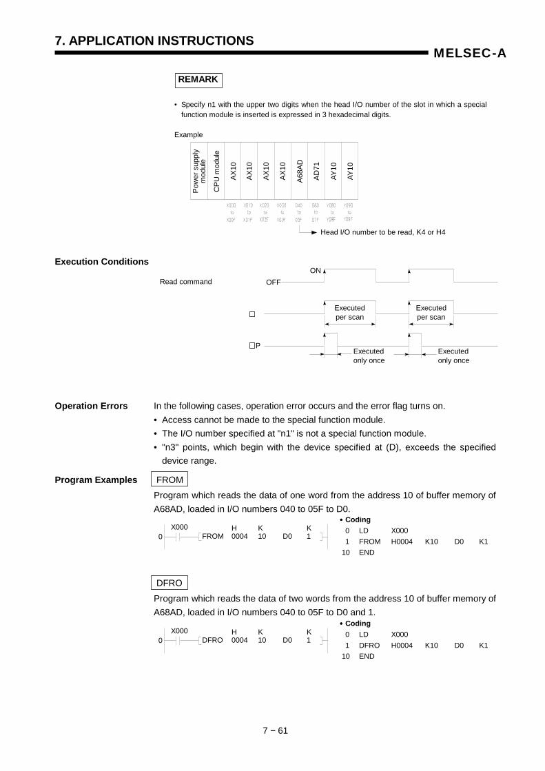
7. APPLICATION INSTRUCTIONS
7 − 61
MELSEC-A
REMARK
• Specify n1 with the upper two digits when the head I/O number of the slot in which a special function module is inserted is expressed in 3 hexadecimal digits. Example
Execution Conditions
Operation Errors In the following cases, operation error occurs and the error flag turns on. • Access cannot be made to the special function module. • The I/O number specified at "n1" is not a special function module. • "n3" points, which begin with the device specified at (D), exceeds the specified device range.
Program Examples FROM Program which reads the data of one word from the address 10 of buffer memory of A68AD, loaded in I/O numbers 040 to 05F to D0.
DFRO Program which reads the data of two words from the address 10 of buffer memory of A68AD, loaded in I/O numbers 040 to 05F to D0 and 1.
Head I/O number to be read, K4 or H4
Pow
er s
uppl
y m
odul
e
CPU
mod
ule
AX10
AX10
AX10
AX10
A68A
D
AD71
AY10
AY10
OFF ON
Executed per scan
Executed per scan
Executed only once
Executed only once
P
Read command
X000 0
H K K FROM 0004 10 D0 1
•••• Coding 0 LD X000 1 FROM H0004 K10 D0 K1 10 END
X000 0
H K K DFRO 0004 10 D0 1
•••• Coding 0 LD X000 1 DFRO H0004 K10 D0 K1 10 END
7. APPLICATION INSTRUCTIONS
7 − 62
MELSEC-A
POINT
If a FROM instruction is executed for a special function module frequently in a short scan time, the objective special function module may fail to process correctly. To execute a FROM instruction for a special function module, set the execu-tion intervals meeting the processing and conversion time of that module using the timer and the constant scan function of it.
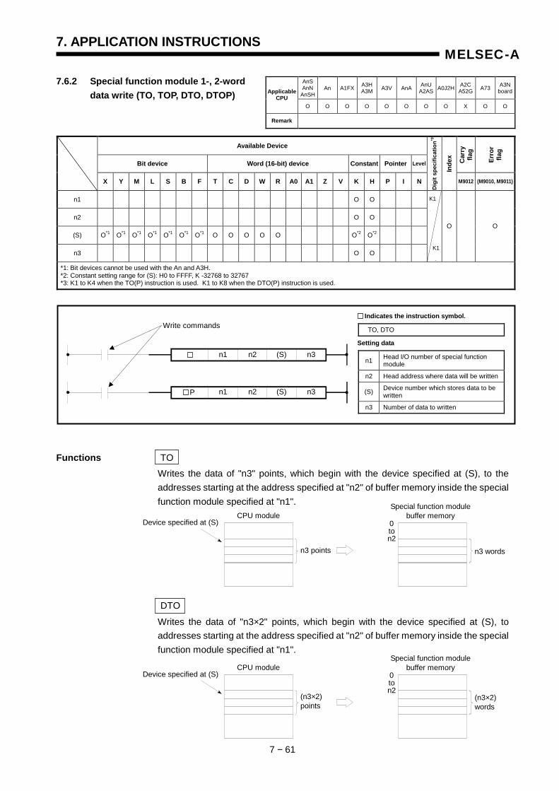
7. APPLICATION INSTRUCTIONS
7 − 61
MELSEC-A
7.6.2 Special function module 1-, 2-word data write (TO, TOP, DTO, DTOP)
Available Device
Bit device Word (16-bit) device Constant Pointer Level Car
ry
flag
Erro
r fla
g
X Y M L S B F T C D W R A0 A1 Z V K H P I N
Dig
it sp
ecifi
catio
n*3
Inde
x
M9012 (M9010, M9011)
n1 O O
n2 O O
(S) O*1 O*1 O*1 O*1 O*1 O*1 O*1 O O O O O O*2 O*2
n3 O O
O O
*1: Bit devices cannot be used with the An and A3H. *2: Constant setting range for (S): H0 to FFFF, K -32768 to 32767 *3: K1 to K4 when the TO(P) instruction is used. K1 to K8 when the DTO(P) instruction is used.
Functions TO Writes the data of "n3" points, which begin with the device specified at (S), to the addresses starting at the address specified at "n2" of buffer memory inside the special function module specified at "n1".
DTO
Writes the data of "n3×2" points, which begin with the device specified at (S), to addresses starting at the address specified at "n2" of buffer memory inside the special function module specified at "n1".
AnSAnN
AnSHAn A1FX A3H
A3M A3V AnA AnU A2AS A0J2H A2C
A52G A73 A3NboardApplicable
CPU O O O O O O O O X O O
Remark
K1
t
K1
t
Special function module buffer memory CPU module
0ton2
Device specified at (S)
n3 points n3 words
Special function module buffer memory CPU module
0ton2
Device specified at (S)
(n3×2) points
(n3×2) words
n3
n3
n1 Head I/O number of special function module
n2 Head address where data will be written
(S) Device number which stores data to be written
n3 Number of data to written
Setting data
TO, DTO
Indicates the instruction symbol.
n1 (S)
n1 (S)P
n2
n2
Write commands
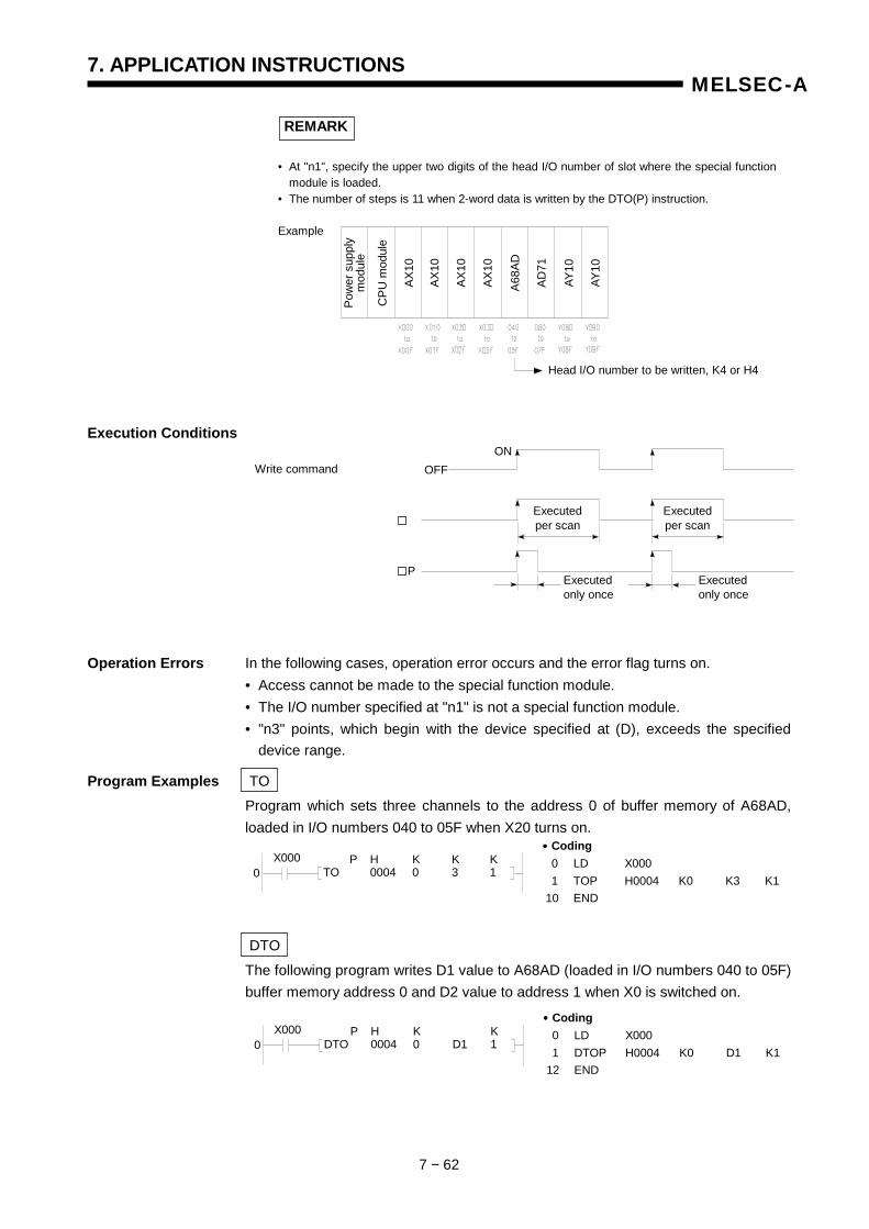
7. APPLICATION INSTRUCTIONS
7 − 62
MELSEC-A
REMARK
• At "n1", specify the upper two digits of the head I/O number of slot where the special function module is loaded. • The number of steps is 11 when 2-word data is written by the DTO(P) instruction. Example
Execution Conditions
Operation Errors In the following cases, operation error occurs and the error flag turns on. • Access cannot be made to the special function module. • The I/O number specified at "n1" is not a special function module. • "n3" points, which begin with the device specified at (D), exceeds the specified device range.
Program Examples TO Program which sets three channels to the address 0 of buffer memory of A68AD, loaded in I/O numbers 040 to 05F when X20 turns on.
DTO The following program writes D1 value to A68AD (loaded in I/O numbers 040 to 05F) buffer memory address 0 and D2 value to address 1 when X0 is switched on.
Head I/O number to be written, K4 or H4
Pow
er s
uppl
y m
odul
e
CPU
mod
ule
AX10
AX10
AX10
AX10
A68A
D
AD71
AY10
AY10
OFF ON
Executed per scan
Executed per scan
Executed only once
Executed only once
P
Write command
X000 0
P H K K K TO 0004 0 3 1
•••• Coding 0 LD X000 1 TOP H0004 K0 K3 K1 10 END
X000 0
P H K K DTO 0004 0 D1 1
•••• Coding 0 LD X000 1 DTOP H0004 K0 D1 K1 12 END

7. APPLICATION INSTRUCTIONS
7 − 63
MELSEC-A
POINT
If a TO instruction is executed for a special function module frequently in a short scan time, the objective special function module may fail to process correctly. To execute a TO instruction for a special function module, set the execution intervals meeting the processing and conversion time of that module using the timer and the constant scan function of it.
7. APPLICATION INSTRUCTIONS
7 − 63
MELSEC-A
7.6.3 Remote terminal module 1- and 2-word data read (FROM, PRC, FROMP, PRC, DFRO, PRC, DFROP, PRC)
Available Device
Bit device Word (16-bit) device Constant Pointer Level Car
ry
flag
Erro
r fla
g
X Y M L S B F T C D W R A0 A1 Z V K H P I N
Dig
it sp
ecifi
catio
n*1
Inde
x
M9012 (M9010, M9011)
n1 O O FROM
n2 O O
(D1) O O O O O DFRO
n3 O O
O O
(D2) O O O O PRC
(D3) O
*1: K1 to K4 when the FROM(P) instruction is used. K1 to K8 when the DFRO(P) instruction is used.
Functions FROM , PRC (1) Reads data of "n3" words which begin with the address specified at "n2" of buffer
memory in the remote terminal module specified at "n1", and stores the data in the devices starting with the one specified at (D1).
AnSAnN
AnSHAn A1FX A3H
A3M A3V AnA AnU A2AS A0J2H A2C
A52G A73 A3NboardApplicable
CPU X X X X X X X X O X X
Remark
K1
t
K1
t
n3
n3
n1
A2C: Head station number of remote terminal module A52G: (Head station number of remote terminal module) + (100)
n2 Head address of data to be read
(D1) Head number of the device which store read data
n3 Number of data to be read
(D2) Number of the device to be turned on at read completion
(D3) Dummy data which has no meaning in program processing
Setting data
FROM, DFRO
Indicates the instruction symbol.
n1 (D1)
n1 (D1)P
n2
n2
Read commands
(D3)(D2)PRC
(D3)(D2)PRC
Not required when the AJ35PTF-R2 RS232C interface unit is used. For details,refer to AJ35PTF-R2 RS-232C interface unit user’s manual.
Remote terminalbuffer memory CPU module
n2
Device specified at (D1)
n3 pointsn3 words
7. APPLICATION INSTRUCTIONS
7 − 64
MELSEC-A
DERO , PRC
(2) Reads data of "n3×2" words which begin with the address specified at "n2" of buffer memory in the remote terminal module specified at "n1", and stores the data in the devices starting with the one specified at (D1).
REMARK
The method for specifying "n1" for an A2C is different from that for an A52G as mentioned below. 1) A2C: Head station number of remote terminal modules is specified at "n1".
2) A52G: specify "n1" with (head number of remote terminal module) + (100). (Example) When the head number of remote terminal module is 9, specify K109 (9+100).
(3) The bit device specified at (D2) is used as a communication complete flag. This device turns ON after execution of the END instruction of the scan during
which communication processing with a specified remote terminal module is completed, and turns OFF after execution of the END instruction of the next scan.
Remote terminal buffer memory CPU module
n2
Device specified at (D1)
(n3×2) points
(n3×2) words
Station No. 1
Station No. 5
AX11C
4 stations
AX11C
4 stations
X000to
X01F
X020to
X03F
Station No. 17
Station No. 13
A2C CPU
Head station number of
remote terminal modules
AY51C
4 stations
A68ADC
4 stations
Y080to
Y09F
060to
07F
Station No. 9
AD61C
4 stations
040 to
05F
Communication endCommunication start
Sequence program flow
Device No. specified at (D2)
7. APPLICATION INSTRUCTIONS
7 − 65
MELSEC-A
(4) Though the data specified at (D3) is dummy data which calls for no processing in the program, specify any output (Y) number at this. Devices specified at (D3) can be freely used in the program.
(5) Data communication is performed according to the data in the communication
request registration areas which are registered by executing the FROM(P) and DFRO(P) instructions, as shown below. Execution of these instructions is completed when data are registered in the communication request registration areas. And then, following instructions are executed.
Once registration is completed by execution of an instruction, communication processing is executed to the end even though the condition signal before the FROM(P)/DFRO(P) instructions is turned OFF.
(6) The device number specified at (D2) is checked. If the same device number was
already specified to execute a processing, registration is not processed after execution of the FROM(P)/DFRO(P) instructions.
(7) After completion of a processing which is executed according to registered data,
the bit device specified at (D2) is turned ON and deleted from the communication request registration areas.
(8) The communication request registration areas can hold data for up to 32
requests. If the number of registration data exceeds 32, operation error occurs and registration processing is not executed.
A2C/A52G
Remote terminal module I/O module
Remote terminal module I/O module
Registration of communication request
Communication request registration areas
K K K FROM 1 18 D10 1
PRC M0 Y000
7. APPLICATION INSTRUCTIONS
7 − 66
MELSEC-A
(9) Status of registration in the communication request registration areas can be confirmed by M9081 and D9081.
M9081: Turns ON when the communication request registration areas are full. Turns OFF when there is a vacant area.
D9081: Stores the number of vacant areas in the communication request registration areas.
M9081 and D9081 can therefore be used as handshake signals for execution of instructions.
(10) If the FROM(P)/DFRO(P) instructions are executed to a remote terminal module
which is communicating with other module, execution of the instructions is again performed to the same remote terminal module immediately after the processing being executed.
Execution Conditions
Operation Errors In the following cases, operation error occurs and the error flag turns ON. • When the station number specified at (n1) is not of a remote terminal. • When "n3" points which start with the device specified at (D1) exceed the specified device range. • When the device specified at (D1) is not a usable device.
Program Examples FROM , PRC A program which reads data of 1 word from address 18 of buffer memory of the AD61C (head station number 1) to D10 when X0 is turned ON.
Device specified at (D2) (Communication complete flag)
OFF
ON
Executed every completion of
communication
Executed every completion of
communication
Executed only once Executed only once P
Read command
Device specified at (D2) (Communication complete flag)
K K K FROM 1 18 D10 1
PRC M0 Y000
0X000
……... M0 turns ON when communication processing is completed.
•••• Coding 0 LD X000 1 FROM K1 K18 D10 K1 10 PRC M0 Y000 17 END

7. APPLICATION INSTRUCTIONS
7 − 67
MELSEC-A
DFRO , PRC A program which reads data of 2 words from address 14 of buffer memory of the AD61C (head station number 1) to D10 and D11 when X0 is turned ON.
K K K DFRO 1 14 D10 1
PRC M0 Y000
0X000
……... M0 turns ON when communication processing is completed.
•••• Coding 0 LD X000 1 DFRO K1 K14 D10 K1 10 PRC M0 Y000 17 END
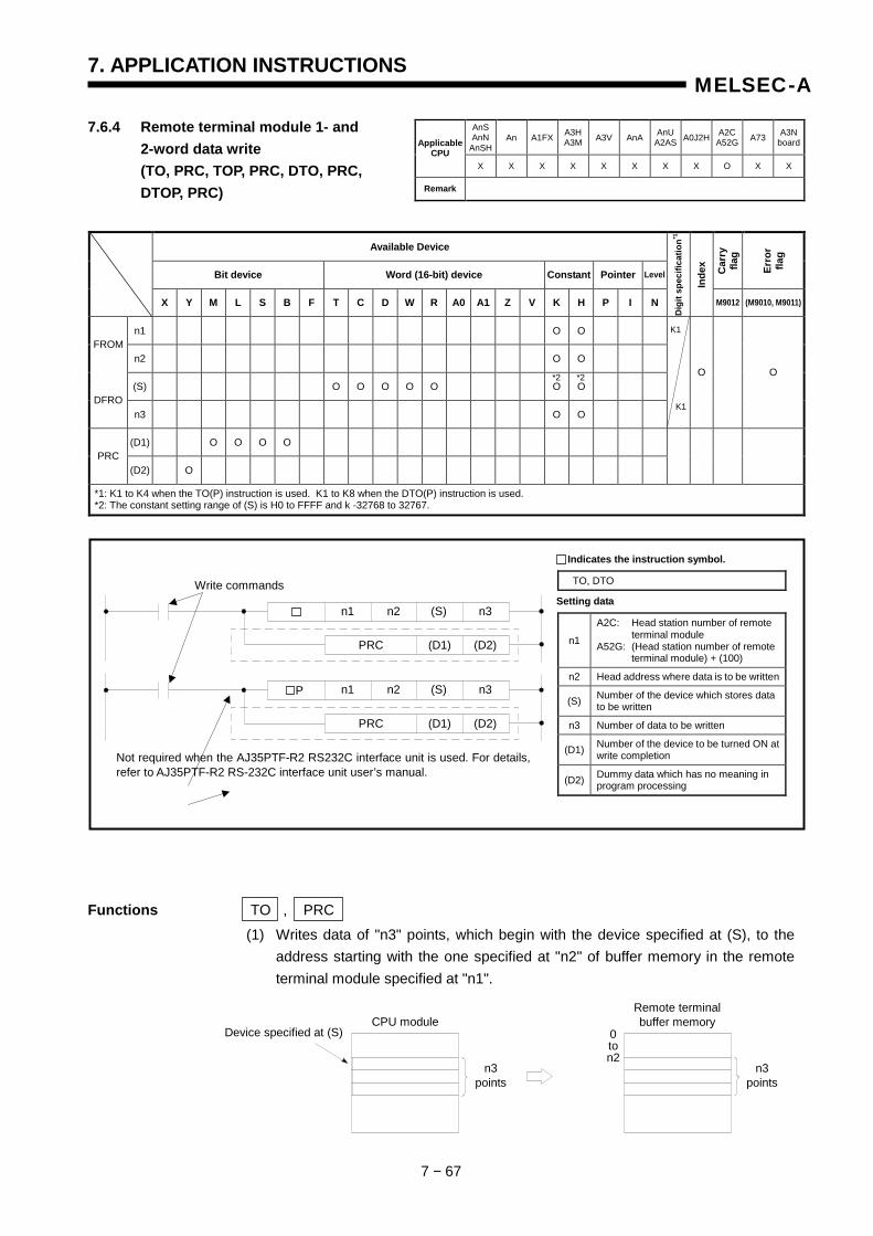
7. APPLICATION INSTRUCTIONS
7 − 67
MELSEC-A
7.6.4 Remote terminal module 1- and 2-word data write (TO, PRC, TOP, PRC, DTO, PRC, DTOP, PRC)
Available Device
Bit device Word (16-bit) device Constant Pointer Level Car
ry
flag
Erro
r fla
g
X Y M L S B F T C D W R A0 A1 Z V K H P I N
Dig
it sp
ecifi
catio
n*1
Inde
x
M9012 (M9010, M9011)
n1 O O FROM
n2 O O
(S) O O O O O O O DFRO
n3 O O
O O
(D1) O O O O PRC
(D2) O
*1: K1 to K4 when the TO(P) instruction is used. K1 to K8 when the DTO(P) instruction is used. *2: The constant setting range of (S) is H0 to FFFF and k -32768 to 32767.
Functions TO , PRC (1) Writes data of "n3" points, which begin with the device specified at (S), to the
address starting with the one specified at "n2" of buffer memory in the remote terminal module specified at "n1".
AnSAnN
AnSHAn A1FX A3H
A3M A3V AnA AnU A2AS A0J2H A2C
A52G A73 A3NboardApplicable
CPU X X X X X X X X O X X
Remark
K1
t
K1
t
*2 *2
n3
n3
n1
A2C: Head station number of remote terminal module A52G: (Head station number of remote terminal module) + (100)
n2 Head address where data is to be written
(S) Number of the device which stores data to be written
n3 Number of data to be written
(D1) Number of the device to be turned ON at write completion
(D2) Dummy data which has no meaning in program processing
Setting data
TO, DTO
Indicates the instruction symbol.
n1 (S)
n1 (S)P
n2
n2
Write commands
(D2)(D1)PRC
(D2)(D1)PRC
Not required when the AJ35PTF-R2 RS232C interface unit is used. For details, refer to AJ35PTF-R2 RS-232C interface unit user’s manual.
Remote terminal buffer memory CPU module
0to n2
Device specified at (S)
n3 points
n3points
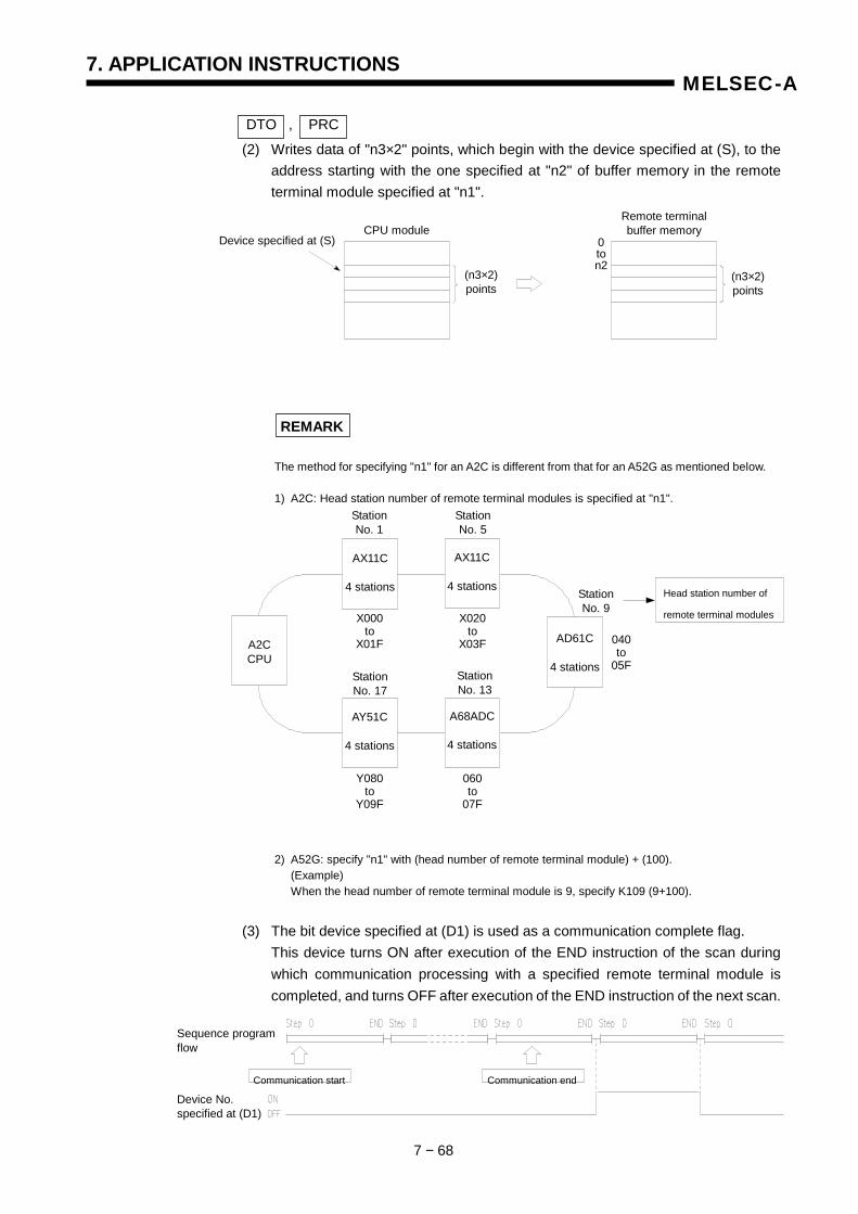
7. APPLICATION INSTRUCTIONS
7 − 68
MELSEC-A
DTO , PRC
(2) Writes data of "n3×2" points, which begin with the device specified at (S), to the address starting with the one specified at "n2" of buffer memory in the remote terminal module specified at "n1".
REMARK
The method for specifying "n1" for an A2C is different from that for an A52G as mentioned below. 1) A2C: Head station number of remote terminal modules is specified at "n1".
2) A52G: specify "n1" with (head number of remote terminal module) + (100). (Example) When the head number of remote terminal module is 9, specify K109 (9+100).
(3) The bit device specified at (D1) is used as a communication complete flag. This device turns ON after execution of the END instruction of the scan during
which communication processing with a specified remote terminal module is completed, and turns OFF after execution of the END instruction of the next scan.
Remote terminal buffer memory CPU module
0ton2
Device specified at (S)
(n3×2) points
(n3×2) points
Station No. 1
Station No. 5
AX11C
4 stations
AX11C
4 stations
X000to
X01F
X020to
X03F
Station No. 17
Station No. 13
A2C CPU
Head station number of
remote terminal modules
AY51C
4 stations
A68ADC
4 stations
Y080to
Y09F
060to
07F
Station No. 9
AD61C
4 stations
040 to
05F
Communication endCommunication start
Sequence program flow
Device No. specified at (D1)
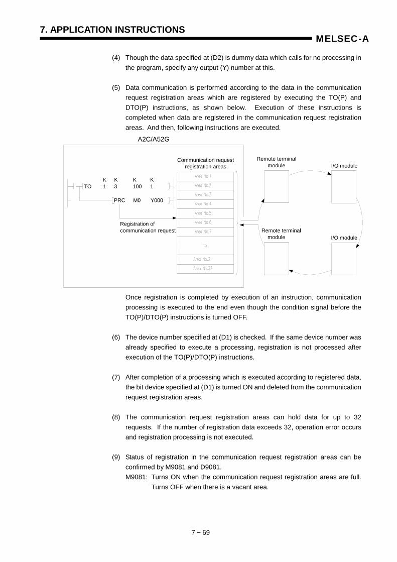
7. APPLICATION INSTRUCTIONS
7 − 69
MELSEC-A
(4) Though the data specified at (D2) is dummy data which calls for no processing in the program, specify any output (Y) number at this.
(5) Data communication is performed according to the data in the communication
request registration areas which are registered by executing the TO(P) and DTO(P) instructions, as shown below. Execution of these instructions is completed when data are registered in the communication request registration areas. And then, following instructions are executed.
Once registration is completed by execution of an instruction, communication processing is executed to the end even though the condition signal before the TO(P)/DTO(P) instructions is turned OFF.
(6) The device number specified at (D1) is checked. If the same device number was
already specified to execute a processing, registration is not processed after execution of the TO(P)/DTO(P) instructions.
(7) After completion of a processing which is executed according to registered data,
the bit device specified at (D1) is turned ON and deleted from the communication request registration areas.
(8) The communication request registration areas can hold data for up to 32
requests. If the number of registration data exceeds 32, operation error occurs and registration processing is not executed.
(9) Status of registration in the communication request registration areas can be
confirmed by M9081 and D9081. M9081: Turns ON when the communication request registration areas are full.
Turns OFF when there is a vacant area.
A2C/A52G
Remote terminal module I/O module
Remote terminal module I/O module
Registration of communication request
Communication request registration areas
K K K K TO 1 3 100 1
PRC M0 Y000
7. APPLICATION INSTRUCTIONS
7 − 70
MELSEC-A
D9081: Stores the number of vacant areas in the communication request registration areas.
M9081 and D9081 can therefore be used as handshake signals at execution of instructions.
(10) If the TO(P)/DTO(P) instructions are executed to a remote terminal module which is communicating with other module, execution of the instructions is again performed to the same remote terminal module immediately after the processing being executed.
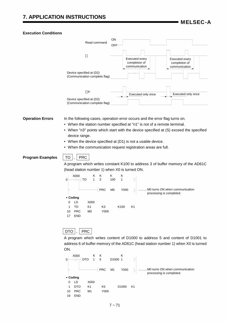
7. APPLICATION INSTRUCTIONS
7 − 71
MELSEC-A
Execution Conditions
Operation Errors In the following cases, operation error occurs and the error flag turns on. • When the station number specified at "n1" is not of a remote terminal. • When "n3" points which start with the device specified at (S) exceed the specified device range. • When the device specified at (D1) is not a usable device. • When the communication request registration areas are full.
Program Examples TO , PRC A program which writes constant K100 to address 3 of buffer memory of the AD61C (head station number 1) when X0 is turned ON.
DTO , PRC A program which writes content of D1000 to address 5 and content of D1001 to address 6 of buffer memory of the AD61C (head station number 1) when X0 is turned ON.
Device specified at (D2) (Communication complete flag)
OFF
ON
Executed every completion of
communication
Executed every completion of
communication
Executed only once Executed only once P
Read command
Device specified at (D2) (Communication complete flag)
K K K K TO 1 3 100 1
PRC M0 Y000
0X000
……... M0 turns ON when communication processing is completed.
•••• Coding 0 LD X000 1 TO K1 K3 K100 K1 10 PRC M0 Y000 17 END
K K K DTO 1 5 D1000 1
PRC M1 Y000
0X000
……... M0 turns ON when communication processing is completed.
•••• Coding 0 LD X000 1 DTO K1 K5 D1000 K1 10 PRC M1 Y000 19 END
7. APPLICATION INSTRUCTIONS
7 − 71
MELSEC-A
7.6.5 Special module/special block 1-, 2-word data read (FROM, FROMP, DFRO, DFROP)
Available Device
Bit device Word (16-bit) device Constant Pointer Level Car
ry
flag
Erro
r fla
g
X Y M L S B F T C D W R A0 A1 Z V K H P I N
Digi
t spe
cific
atio
n
Inde
x
M9012 (M9010, M9011)
n1 O O
n2 O O
(D) O O O O O O O O O O
n3 O O
* O O
*: K1 to K4 when the FROM(P) instruction is used. K1 to K8 when the DFRO(P) instruction is used.
Function FROM Reads the n3 words of data from the buffer memory address specified by n2 in the special module/special block specified by n1 and writes the data to the A1FXCPU beginning with the device number specified by (D).
AnSAnN
AnSHAn A1FX A3H
A3M A3V AnA AnU A2AS A0J2H A2C
A52G A73 A3NboardApplicable
CPU X X O X X X X X X X X
Remark
n3
n3
n1 Sets the position of the special module or the special block counted from the A1FXCPU (0 to 7).
n2 The head address of the special module or the special block where the data is read.
(D) The device number of the A1FXCPU where the read data is stored.
n3 Number of data to be read
Setting data
FROM, DFRO
Indicates the instruction symbol.
n1 (D)
n1 (D)P
n2
n2
Read commands
Buffer memory in the special module/
special block A1FXCPU
n2
Device number specified by (D)
n3 pointsn3 words

7. APPLICATION INSTRUCTIONS
7 − 72
MELSEC-A
DFRO
Reads the (2×n3) words of data from the buffer memory address specified by n2 in the special module/special block specified by n1 and writes the data to the A1FXCPU beginning with the device number specified by (D).
Execution FROM and DFRO instructions are executed every scan while the read instruction is Conditions ON.
FROMP and DFROP instructions are executed only once at the rising edge (OFF → ON) of the read instruction.
Operation Errors In the following cases, operation error occurs and the error flag turns on. • Access to a special module/special block is not possible. • n1 designation is other than 0 to 7 • When "n3" points which start with the device specified at (S) exceed the specified device range.
REMARK
Set the order number of the special module/special block in question to "n1", counted from the A1FXCPU.
Buffer memory in the special module/
special block A1FXCPU
n2
Device number specified by (D)
2×n3 points
2×n3 words
OFF ON
Executed per scan
Executed per scan
Executed only once
Executed only once
P
Read command
A1FXCPU Expansion unit/ Expansion block
Special module/Special block
Special module/Special block
Set 0 at n1 Set 1 at n1
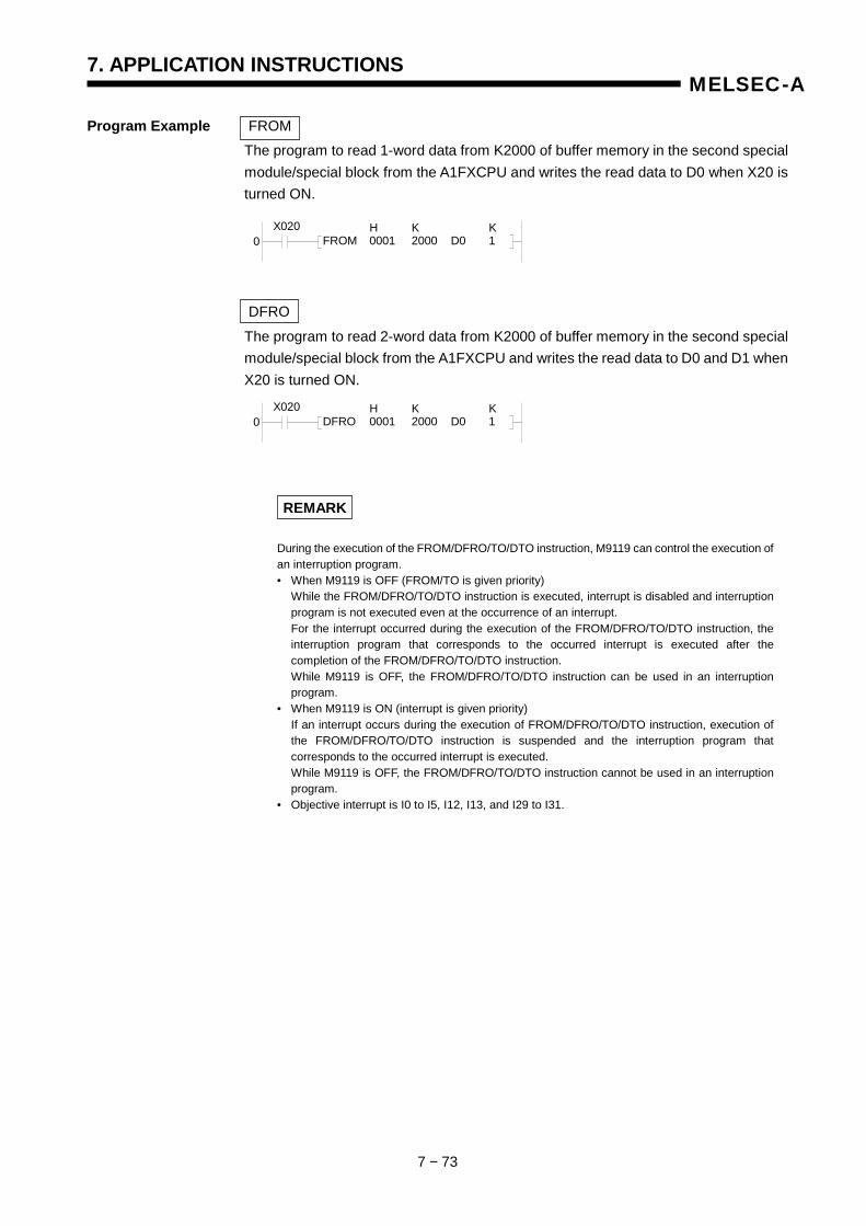
7. APPLICATION INSTRUCTIONS
7 − 73
MELSEC-A
Program Example FROM The program to read 1-word data from K2000 of buffer memory in the second special module/special block from the A1FXCPU and writes the read data to D0 when X20 is turned ON.
DFRO
The program to read 2-word data from K2000 of buffer memory in the second special module/special block from the A1FXCPU and writes the read data to D0 and D1 when X20 is turned ON.
REMARK
During the execution of the FROM/DFRO/TO/DTO instruction, M9119 can control the execution of an interruption program. • When M9119 is OFF (FROM/TO is given priority) While the FROM/DFRO/TO/DTO instruction is executed, interrupt is disabled and interruption program is not executed even at the occurrence of an interrupt. For the interrupt occurred during the execution of the FROM/DFRO/TO/DTO instruction, the interruption program that corresponds to the occurred interrupt is executed after the completion of the FROM/DFRO/TO/DTO instruction. While M9119 is OFF, the FROM/DFRO/TO/DTO instruction can be used in an interruption program. • When M9119 is ON (interrupt is given priority) If an interrupt occurs during the execution of FROM/DFRO/TO/DTO instruction, execution of the FROM/DFRO/TO/DTO instruction is suspended and the interruption program that corresponds to the occurred interrupt is executed. While M9119 is OFF, the FROM/DFRO/TO/DTO instruction cannot be used in an interruption program. • Objective interrupt is I0 to I5, I12, I13, and I29 to I31.
X020 0
H K K FROM 0001 2000 D0 1
X020 0
H K K DFRO 0001 2000 D0 1
7. APPLICATION INSTRUCTIONS
7 − 74
MELSEC-A
7.6.6 Special module/special block 1-, 2-word data write (TO, TOP, DTO, DTOP)
Available Device
Bit device Word (16-bit) device Constant Pointer Level Car
ry
flag
Erro
r fla
g
X Y M L S B F T C D W R A0 A1 Z V K H P I N
Digi
t spe
cific
atio
n
Inde
x
M9012 (M9010, M9011)
n1 O O
n2 O O
(S) O O O O O O O O O O O O
n3 O O
* O O
*: K1 to K4 when the TO(P) instruction is used. K1 to K8 when the DTO(P) instruction is used. The constant setting range of (S) is H0 to FFFF and k -32765 to 32767.
Function TO Writes the n3-point data from the device number specified by (S) to the buffer memory addresses beginning with the address specified by n2 in the special module/special block specified by n1.
AnSAnN
AnSHAn A1FX A3H
A3M A3V AnA AnU A2AS A0J2H A2C
A52G A73 A3NboardApplicable
CPU X X O X X X X X X X X
Remark
n3
n3
n1 Sets the position of the special module or the special block counted from the A1FXCPU (0 to 7).
n2 The head address of the special module or the special block where the data is read.
(S) The device number of the A1FXCPU where the read data is stored.
n3 Number of data to be read
Setting data
TO, DTO
Indicates the instruction symbol.
n1 (S)
n1 (S)P
n2
n2
Write commands
Buffer memory in the special module/
special block A1FXCPU
n2
Device specified at (S)
n3 points n3 words
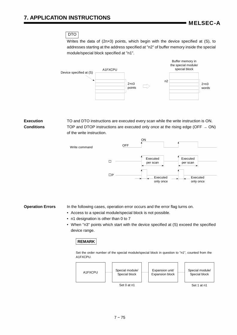
7. APPLICATION INSTRUCTIONS
7 − 75
MELSEC-A
DTO
Writes the data of (2n×3) points, which begin with the device specified at (S), to addresses starting at the address specified at "n2" of buffer memory inside the special module/special block specified at "n1".
Execution TO and DTO instructions are executed every scan while the write instruction is ON. Conditions TOP and DTOP instructions are executed only once at the rising edge (OFF → ON) of the write instruction.
Operation Errors In the following cases, operation error occurs and the error flag turns on. • Access to a special module/special block is not possible. • n1 designation is other than 0 to 7 • When "n3" points which start with the device specified at (S) exceed the specified device range.
REMARK
Set the order number of the special module/special block in question to "n1", counted from the A1FXCPU.
Buffer memory in the special module/
special block A1FXCPU
n2
Device specified at (S)
2×n3 points
2×n3 words
OFF
ON
Executed per scan
Executed per scan
Executed only once
Executed only once
P
Write command
A1FXCPU Expansion unit/ Expansion block
Special module/Special block
Special module/Special block
Set 0 at n1 Set 1 at n1
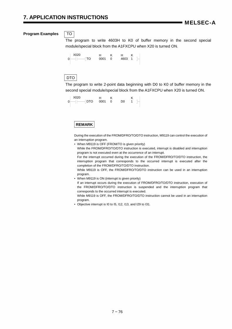
7. APPLICATION INSTRUCTIONS
7 − 76
MELSEC-A
Program Examples TO The program to write 4603H to K0 of buffer memory in the second special module/special block from the A1FXCPU when X20 is turned ON.
DTO The program to write 2-point data beginning with D0 to K0 of buffer memory in the second special module/special block from the A1FXCPU when X20 is turned ON.
REMARK
During the execution of the FROM/DFRO/TO/DTO instruction, M9119 can control the execution of an interruption program. • When M9119 is OFF (FROM/TO is given priority) While the FROM/DFRO/TO/DTO instruction is executed, interrupt is disabled and interruption program is not executed even at the occurrence of an interrupt. For the interrupt occurred during the execution of the FROM/DFRO/TO/DTO instruction, the interruption program that corresponds to the occurred interrupt is executed after the completion of the FROM/DFRO/TO/DTO instruction. While M9119 is OFF, the FROM/DFRO/TO/DTO instruction can be used in an interruption program. • When M9119 is ON (interrupt is given priority) If an interrupt occurs during the execution of FROM/DFRO/TO/DTO instruction, execution of the FROM/DFRO/TO/DTO instruction is suspended and the interruption program that corresponds to the occurred interrupt is executed. While M9119 is OFF, the FROM/DFRO/TO/DTO instruction cannot be used in an interruption program. • Objective interrupt is I0 to I5, I12, I13, and I29 to I31.
X020 0
H K H K TO 0001 0 4603 1
X020 0
H K K DTO 0001 0 D0 1

7. APPLICATION INSTRUCTIONS
7 − 77
MELSEC-A
7.7 FOR to NEXT Instructions
7.7.1 FOR to NEXT (FOR, NEXT)
Available Device
Bit device Word (16-bit) device Constant Pointer Level Car
ry
flag
Erro
r fla
g
X Y M L S B F T C D W R A0 A1 Z V K H P I N
Digi
t spe
cific
atio
n
Inde
x
M9012 (M9010, M9011)
n O O O O O O O O O O O O
Functions (1) When the processing of FOR to NEXT instructions is executed "n" times unconditionally, performs the processing of the next step to the NEXT Instruction.
(2) At "n" , 1 to 32767 can be specified. When - 32767 to 0 has been specified, the
same processing an n = 1 is performed. (positive integers) (3) When it is not desired to execute the processing of FOR to NEXT instructions,
cause a jump by use of the CJ or SCJ instruction
Applicable CPU All CPUs
FOR n
NEXT
Repeat program
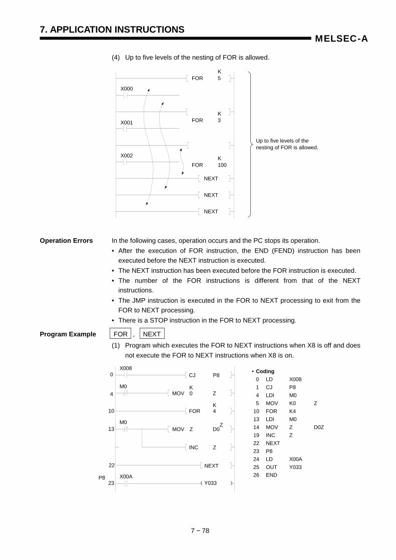
7. APPLICATION INSTRUCTIONS
7 − 78
MELSEC-A
(4) Up to five levels of the nesting of FOR is allowed.
Operation Errors In the following cases, operation occurs and the PC stops its operation. • After the execution of FOR instruction, the END (FEND) instruction has been executed before the NEXT instruction is executed. • The NEXT instruction has been executed before the FOR instruction is executed. • The number of the FOR instructions is different from that of the NEXT instructions. • The JMP instruction is executed in the FOR to NEXT processing to exit from the FOR to NEXT processing. • There is a STOP instruction in the FOR to NEXT processing.
Program Example FOR , NEXT (1) Program which executes the FOR to NEXT instructions when X8 is off and does
not execute the FOR to NEXT instructions when X8 is on.
NEXT
NEXT
NEXT
X000
X001
X002
Up to five levels of the nesting of FOR is allowed.
K FOR 5
K FOR 3
K FOR 100
( )
X008
M0
M0
0
4
10
13
22
23 P8
CJ P8
K
FOR 4
INC Z
MOV Z D0
MOV 0 Z
Z
NEXT
Y033
• Coding 0 LD X008 1 CJ P8 4 LDI M0 5 MOV K0 Z 10 FOR K4 13 LDI M0 14 MOV Z D0Z 19 INC Z 22 NEXT 23 P8 24 LD X00A 25 OUT Y033 26 END X00A
K

7. APPLICATION INSTRUCTIONS
7 − 79
MELSEC-A
7.8 Local, Remote I/O Station Access Instructions
Local, remote I/O station access instructions are used to transfer data in a data link system. Four instructions are provided as shown below. The local and remote I/O station access instructions can be used in the sequence program of the master station only.
Classification Instruction Symbol Ref. Page
Read LRDP 7-80 Local station Write LWTP 7-80
Read RFRP 7-86 Remote I/O station Write RTOP 7-86
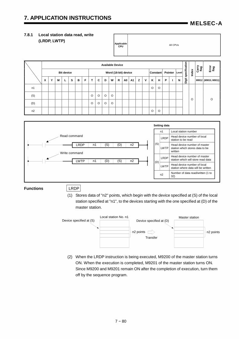
7. APPLICATION INSTRUCTIONS
7 − 80
MELSEC-A
7.8.1 Local station data read, write (LRDP, LWTP)
Available Device
Bit device Word (16-bit) device Constant Pointer Level Car
ry
flag
Erro
r fla
g
X Y M L S B F T C D W R A0 A1 Z V K H P I N
Digi
t spe
cific
atio
n
Inde
x
M9012 (M9010, M9011)
n1 O O
(S) O O O O
(D) O O O O
n2 O O
O O
Functions LRDP (1) Stores data of "n2" points, which begin with the device specified at (S) of the local
station specified at "n1", to the devices starting with the one specified at (D) of the master station.
(2) When the LRDP instruction is being executed, M9200 of the master station turns ON. When the execution is completed, M9201 of the master station turns ON.
Since M9200 and M9201 remain ON after the completion of execution, turn them off by the sequence program.
Applicable CPU All CPUs
LRDP n1 (S) (D) n2
LWTP n1 (D) (S) n2
Write command
Read command n1 Local station number
LRDP Head device number of local station to be read
(S)LWTP
Head device number of master station which stores data to be written
LRDP Head device number of master station which will store read data
(D)LWTP Head device number of local
station where data will be written
n2 Number of data read/written (1 to 32)
Setting data
Master stationDevice specified at (S)
Local station No. n1Device specified at (D)
n2 points
Transfer
n2 points
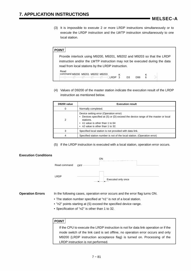
7. APPLICATION INSTRUCTIONS
7 − 81
MELSEC-A
(3) It is impossible to execute 2 or more LRDP instructions simultaneously or to execute the LRDP instruction and the LWTP instruction simultaneously to one local station.
POINT
Provide interlock using M9200, M9201, M9202 and M9203 so that the LRDP instruction and/or the LWTP instruction may not be executed during the data read from local stations by the LRDP instruction.
(4) Values of D9200 of the master station indicate the execution result of the LRDP instruction as mentioned below.
D9200 value Execution result
0 Normally completed.
2
Device setting error (Operation error) • Devices specified at (S) or (D) exceed the device range of the master or local stations. • n1 value is other than 1 to 64 • n2 value is other than 1 to 32.
3 Specified local station is not provided with data link.
4 Specified station number is not of the local station. (Operation error)
(5) If the LRDP instruction is executed with a local station, operation error occurs.
Execution Conditions
Operation Errors In the following cases, operation error occurs and the error flag turns ON.
• The station number specified at "n1" is not of a local station. • "n2" points starting at (S) exceed the specified device range. • Specification of "n2" is other than 1 to 32.
POINT
If the CPU to execute the LRDP instruction is not for data link operation or if the mode switch of the link card is set offline, no operation error occurs and only M9200 (LRDP instruction acceptance flag) is turned on. Processing of the LRDP instruction is not performed.
Read command M9200 M9201 M9202 M9203 K K
LRDP 3 D3 D99 6
Read command
Executed only once LRDP
OFF
ON
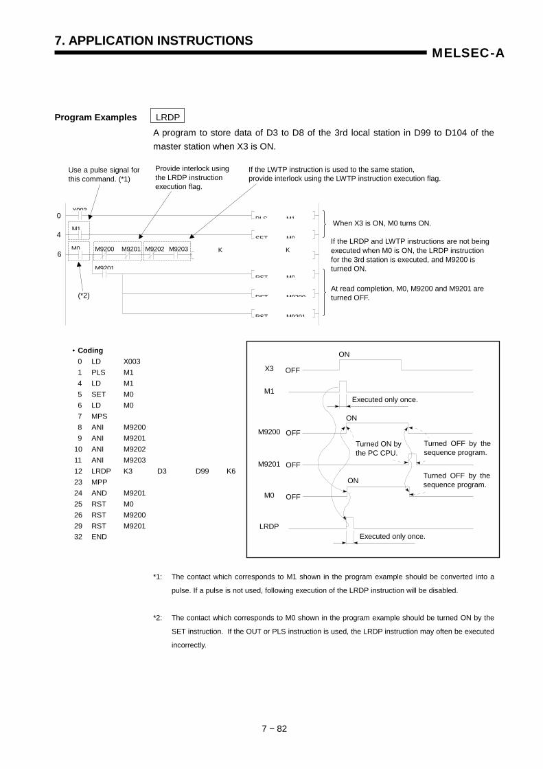
7. APPLICATION INSTRUCTIONS
7 − 82
MELSEC-A
Program Examples LRDP A program to store data of D3 to D8 of the 3rd local station in D99 to D104 of the master station when X3 is ON.
*1: The contact which corresponds to M1 shown in the program example should be converted into a
pulse. If a pulse is not used, following execution of the LRDP instruction will be disabled.
*2: The contact which corresponds to M0 shown in the program example should be turned ON by the
SET instruction. If the OUT or PLS instruction is used, the LRDP instruction may often be executed
incorrectly.
• Coding 0 LD X003 1 PLS M1 4 LD M1 5 SET M0 6 LD M0 7 MPS 8 ANI M9200 9 ANI M9201 10 ANI M9202 11 ANI M9203 12 LRDP K3 D3 D99 K6 23 MPP 24 AND M9201 25 RST M0 26 RST M9200 29 RST M9201 32 END
Use a pulse signal forthis command. (*1)
Provide interlock using the LRDP instruction execution flag.
If the LWTP instruction is used to the same station, provide interlock using the LWTP instruction execution flag.
X003
M1
M0 M9200 M9201 M9202 M9203
PLS M1
K K
M9201
SET M0
RST M0
RST M9200
RST M9201
(*2)
When X3 is ON, M0 turns ON.
If the LRDP and LWTP instructions are not beingexecuted when M0 is ON, the LRDP instruction for the 3rd station is executed, and M9200 is turned ON.
At read completion, M0, M9200 and M9201 are turned OFF.
0
4
6
Turned OFF by thesequence program.
Turned OFF by the sequence program.
Turned ON by the PC CPU.
Executed only once.
Executed only once.
M9200
M9201
M0
M1
X3
LRDP
OFF
OFF
OFF
OFF
ON
ON
ON
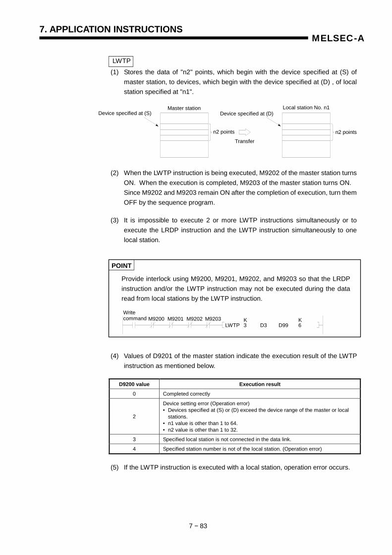
7. APPLICATION INSTRUCTIONS
7 − 83
MELSEC-A
LWTP (1) Stores the data of "n2" points, which begin with the device specified at (S) of
master station, to devices, which begin with the device specified at (D) , of local station specified at "n1".
(2) When the LWTP instruction is being executed, M9202 of the master station turns ON. When the execution is completed, M9203 of the master station turns ON.
Since M9202 and M9203 remain ON after the completion of execution, turn them OFF by the sequence program.
(3) It is impossible to execute 2 or more LWTP instructions simultaneously or to execute the LRDP instruction and the LWTP instruction simultaneously to one local station.
POINT
Provide interlock using M9200, M9201, M9202, and M9203 so that the LRDP instruction and/or the LWTP instruction may not be executed during the data read from local stations by the LWTP instruction.
(4) Values of D9201 of the master station indicate the execution result of the LWTP instruction as mentioned below.
D9200 value Execution result
0 Completed correctly
2
Device setting error (Operation error) • Devices specified at (S) or (D) exceed the device range of the master or local stations. • n1 value is other than 1 to 64. • n2 value is other than 1 to 32.
3 Specified local station is not connected in the data link.
4 Specified station number is not of the local station. (Operation error)
(5) If the LWTP instruction is executed with a local station, operation error occurs.
Master stationDevice specified at (S)
Local station No. n1Device specified at (D)
n2 points
Transfer
n2 points
Write command M9200 M9201 M9202 M9203 K K
LWTP 3 D3 D99 6
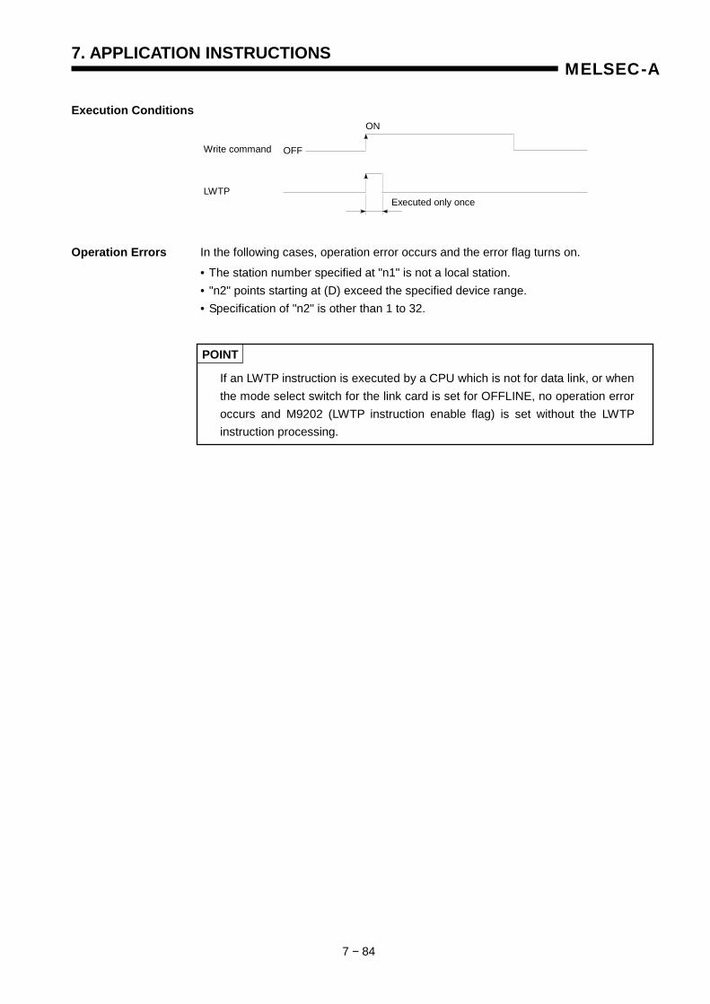
7. APPLICATION INSTRUCTIONS
7 − 84
MELSEC-A
Execution Conditions
Operation Errors In the following cases, operation error occurs and the error flag turns on.
• The station number specified at "n1" is not a local station. • "n2" points starting at (D) exceed the specified device range. • Specification of "n2" is other than 1 to 32.
POINT
If an LWTP instruction is executed by a CPU which is not for data link, or when the mode select switch for the link card is set for OFFLINE, no operation error occurs and M9202 (LWTP instruction enable flag) is set without the LWTP instruction processing.
Write command
Executed only once LWTP
ON
OFF
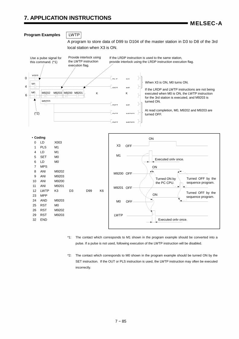
7. APPLICATION INSTRUCTIONS
7 − 85
MELSEC-A
Program Examples LWTP A program to store data of D99 to D104 of the master station in D3 to D8 of the 3rd local station when X3 is ON.
*1: The contact which corresponds to M1 shown in the program example should be converted into a
pulse. If a pulse is not used, following execution of the LWTP instruction will be disabled.
*2: The contact which corresponds to M0 shown in the program example should be turned ON by the
SET instruction. If the OUT or PLS instruction is used, the LWTP instruction may often be executed
incorrectly.
Use a pulse signal forthis command. (*1)
Provide interlock using the LWTP instruction execution flag.
If the LRDP instruction is used to the same station, provide interlock using the LRDP instruction execution flag.
X003
M1
M0 M9202 M9203 M9200 M9201
PLS M1
K K
M9203
SET M0
RST M0
RST M9202
RST M9203
(*2)
When X3 is ON, M0 turns ON.
If the LRDP and LWTP instructions are not being executed when M0 is ON, the LWTP instruction for the 3rd station is executed, and M9203 is turned ON.
At read completion, M0, M9202 and M9203 areturned OFF.
0
4
6
• Coding 0 LD X003 1 PLS M1 4 LD M1 5 SET M0 6 LD M0 7 MPS 8 ANI M9202 9 ANI M9203 10 ANI M9200 11 ANI M9201 12 LWTP K3 D3 D99 K6 23 MPP 24 AND M9203 25 RST M0 26 RST M9202 29 RST M9203 32 END
Turned OFF by thesequence program.
Turned OFF by the sequence program.
Turned ON by the PC CPU.
Executed only once.
Executed only once.
M9200
M9201
M0
M1
X3
LWTP
OFF
OFF
OFF
OFF
ON
ON
ON
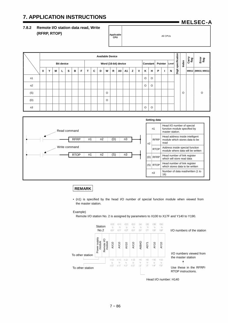
7. APPLICATION INSTRUCTIONS
7 − 86
MELSEC-A7.8.2 Remote I/O station data read, Write
(RFRP, RTOP)
Available Device
Bit device Word (16-bit) device Constant Pointer Level Car
ry
flag
Erro
r fla
g
X Y M L S B F T C D W R A0 A1 Z V K H P I N
Digi
t spe
cific
atio
n
Inde
x
M9012 (M9010, M9011)
n1 O O
n2 O O
(S) O
(D) O
n3 O O
O O
REMARK
• (n1) is specified by the head I/O number of special function module when viewed from the master station. Example) Remote I/O station No. 2 is assigned by parameters to X100 to X17F and Y140 to Y190.
Applicable CPU All CPUs
RFRP n1 n2 (D) n3
RTOP n1 n2 (S) n3
Write command
Read command n1
Head I/O number of special function module specified by master station.
RFRPHead address inside intelligent module which stores data to be read n2
RTOP Address inside special function module where data will be written
(D) RFRP Head number of link register which will store read data
(S) RTOP Head number of link register which stores data to be written
n3 Number of data read/written (1 to 16)
Setting data
StationNo.2
To other station
To other station
Head I/O number: H140
Use these in the RFRP/ RTOP instructions.
I/O numbers viewed from the master station
I/O numbers of the station
Pow
er s
uppi
y m
odul
e R
emot
e I/O
m
odul
e
AX10
AX10
AX10
A68A
D
AD71
AY10
AY10
AX10
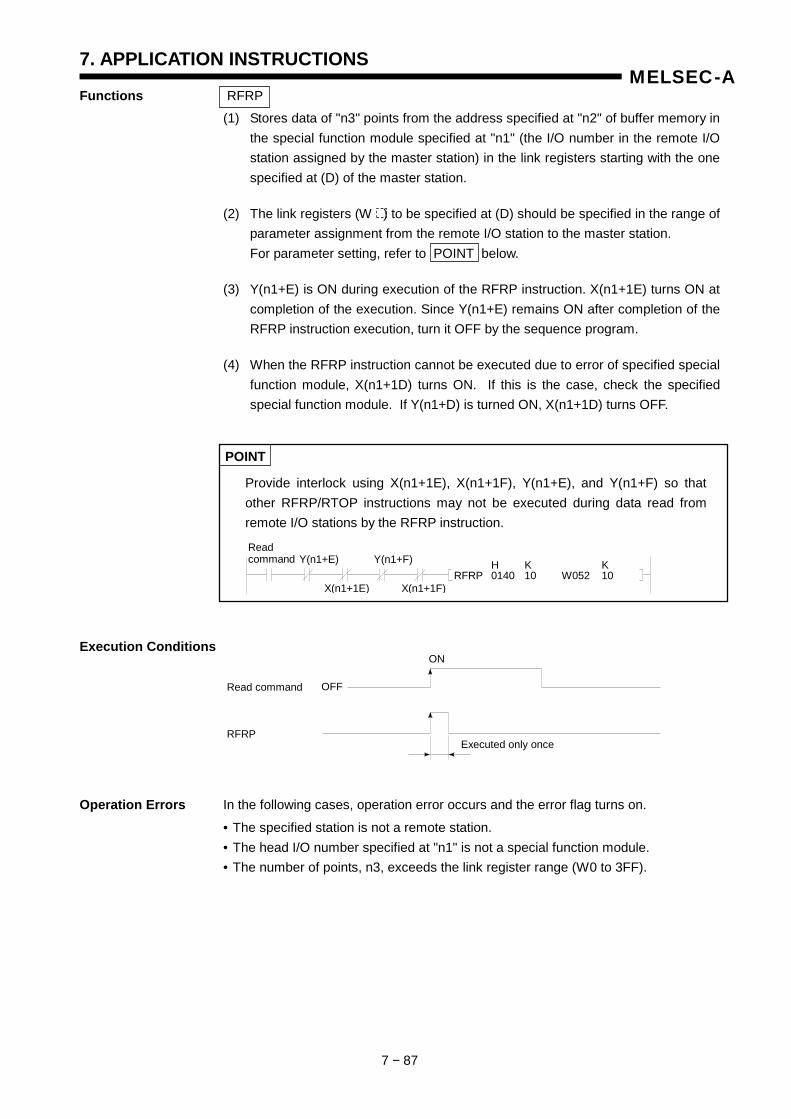
7. APPLICATION INSTRUCTIONS
7 − 87
MELSEC-AFunctions RFRP
(1) Stores data of "n3" points from the address specified at "n2" of buffer memory in the special function module specified at "n1" (the I/O number in the remote I/O station assigned by the master station) in the link registers starting with the one specified at (D) of the master station.
(2) The link registers (W ) to be specified at (D) should be specified in the range of parameter assignment from the remote I/O station to the master station.
For parameter setting, refer to POINT below.
(3) Y(n1+E) is ON during execution of the RFRP instruction. X(n1+1E) turns ON at completion of the execution. Since Y(n1+E) remains ON after completion of the RFRP instruction execution, turn it OFF by the sequence program.
(4) When the RFRP instruction cannot be executed due to error of specified special function module, X(n1+1D) turns ON. If this is the case, check the specified special function module. If Y(n1+D) is turned ON, X(n1+1D) turns OFF.
POINT
Provide interlock using X(n1+1E), X(n1+1F), Y(n1+E), and Y(n1+F) so that other RFRP/RTOP instructions may not be executed during data read from remote I/O stations by the RFRP instruction.
Execution Conditions
Operation Errors In the following cases, operation error occurs and the error flag turns on.
• The specified station is not a remote station. • The head I/O number specified at "n1" is not a special function module. • The number of points, n3, exceeds the link register range (W0 to 3FF).
Read command Y(n1+E) Y(n1+F) H K K
RFRP 0140 10 W052 10 X(n1+1E) X(n1+1F)
Read command
Executed only once RFRP
OFF
ON
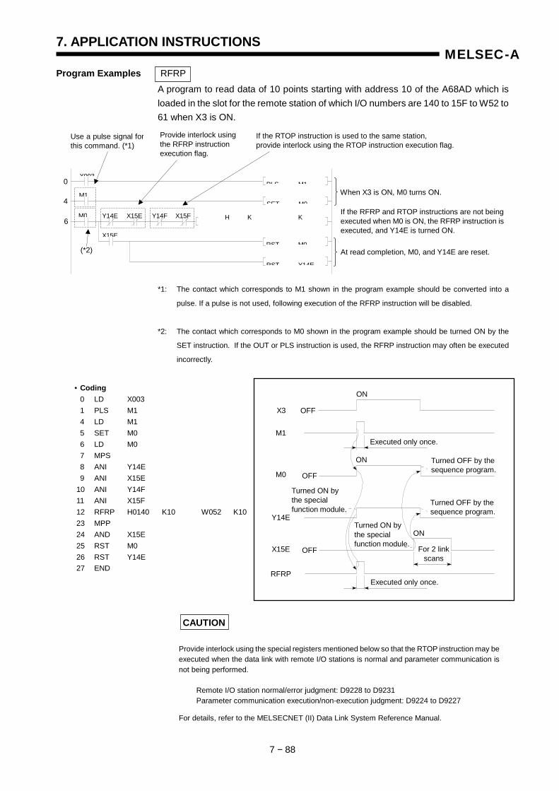
7. APPLICATION INSTRUCTIONS
7 − 88
MELSEC-AProgram Examples RFRP
A program to read data of 10 points starting with address 10 of the A68AD which is loaded in the slot for the remote station of which I/O numbers are 140 to 15F to W52 to 61 when X3 is ON.
*1: The contact which corresponds to M1 shown in the program example should be converted into a
pulse. If a pulse is not used, following execution of the RFRP instruction will be disabled.
*2: The contact which corresponds to M0 shown in the program example should be turned ON by the
SET instruction. If the OUT or PLS instruction is used, the RFRP instruction may often be executed
incorrectly.
CAUTION
Provide interlock using the special registers mentioned below so that the RTOP instruction may be executed when the data link with remote I/O stations is normal and parameter communication is not being performed. Remote I/O station normal/error judgment: D9228 to D9231 Parameter communication execution/non-execution judgment: D9224 to D9227
For details, refer to the MELSECNET (II) Data Link System Reference Manual.
• Coding 0 LD X003 1 PLS M1 4 LD M1 5 SET M0 6 LD M0 7 MPS 8 ANI Y14E 9 ANI X15E 10 ANI Y14F 11 ANI X15F 12 RFRP H0140 K10 W052 K10 23 MPP 24 AND X15E 25 RST M0 26 RST Y14E 27 END
0
4
6
Use a pulse signal forthis command. (*1)
Provide interlock using the RFRP instruction execution flag.
If the RTOP instruction is used to the same station, provide interlock using the RTOP instruction execution flag.
X003
M1
M0 Y14E X15E Y14F X15F
X15E
PLS M1
H K K
SET M0
RST M0
RST Y14E
When X3 is ON, M0 turns ON.
If the RFRP and RTOP instructions are not being executed when M0 is ON, the RFRP instruction is executed, and Y14E is turned ON.
At read completion, M0, and Y14E are reset. (*2)
Executed only once.
Turned OFF by the sequence program.
Turned ON by the special function module.
For 2 link scans
Executed only once.
Turned OFF by the sequence program.
Turned ON by the special function module.
RFRP
X15E
Y14E
M0
M1
X3
ON
ON
ON
OFF
OFF
OFF

7. APPLICATION INSTRUCTIONS
7 − 89
MELSEC-AFunctions RTOP
(1) Writes data of "n3" points of the link registers (W ) starting with the one specified at (S) to addresses starting with the one specified at "n2" of buffer memory in the special function module of which I/O number is specified at "n1" (the I/O number in the remote I/O station assigned by the master station).
(2) The link registers (W ) to be specified at (S) should be specified in the range of parameter assignment from the master station to the remote I/O station.
For parameter setting, refer to POINT below.
(3) It is not allowed to use two or more RTOP instructions or to use the RTOP and RFRP instructions simultaneously with a special function module which has the same I/O number.
POINT
Provide interlock using X(n1+1E), X(n1+1F), Y(n1+E), and Y(n1+F) so that other RTOP instructions may not be executed during data write to remote I/O stations by the RTOP instruction.
(4) Y(n1+F) is ON during execution of the RTOP instruction. X(n1+1F) turns ON at completion of the execution. Since Y(n1+F) remains ON after completion of the RTOP instruction execution, turn it OFF by the sequence program.
(5) When the RTOP instruction cannot be executed due to error of specified special function module, X(n1+1D) turns ON. If this is the case, check the specified special function module. If Y(n1+D) is turned ON, X(n1+1D) turns OFF.
Execution Conditions
Operation Errors In the following cases, operation error occurs and the error flag turns on.
• The specified station is not a remote station. • The head I/O number specified at "n1" is not a special function module. • The number of points, n3, exceeds the link register range (W0 to 3FF).
Write instruction Y(n1+F) Y(n1+E) H K K
RTOP 0140 10 W052 10 X(n1+1F) X(n1+1E)
Read command
Executed only once RFRP
OFF
ON
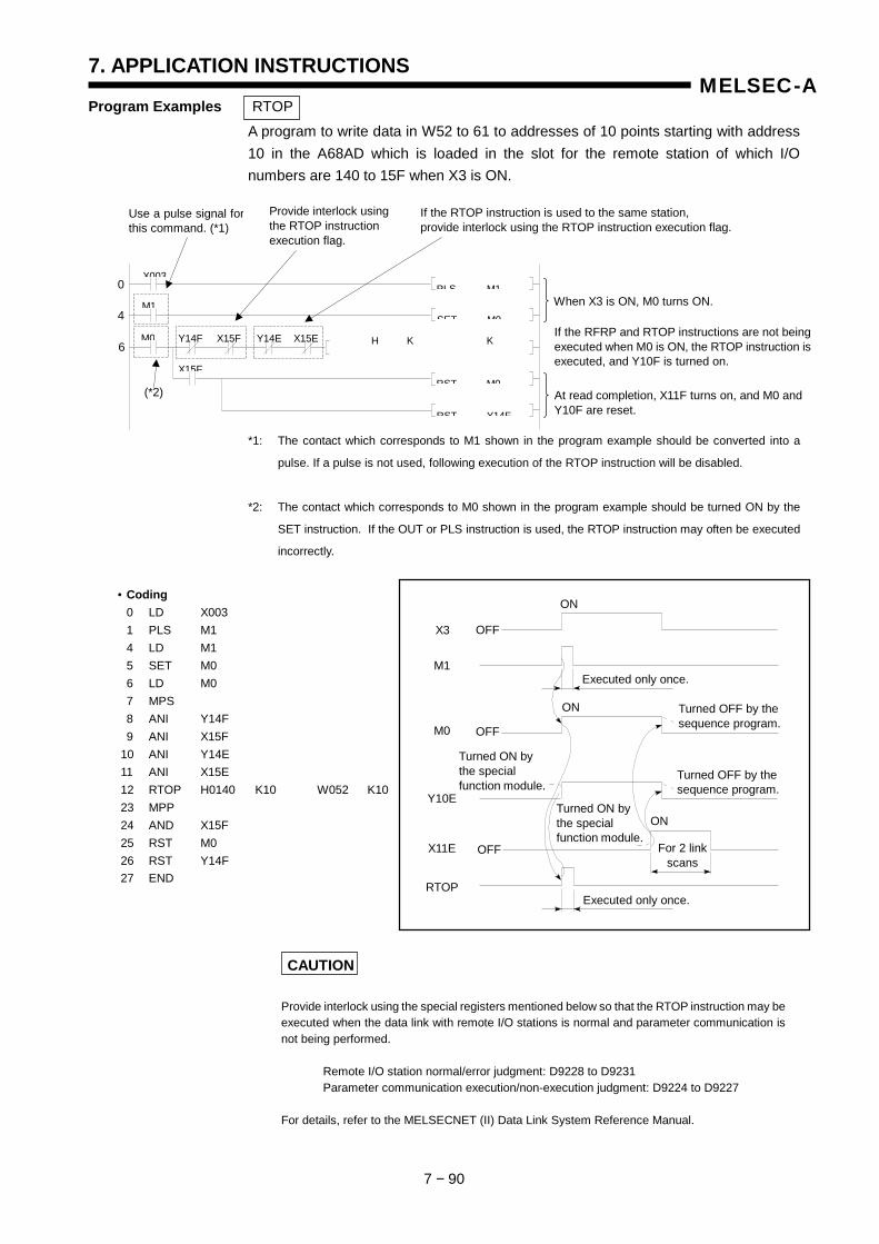
7. APPLICATION INSTRUCTIONS
7 − 90
MELSEC-AProgram Examples RTOP
A program to write data in W52 to 61 to addresses of 10 points starting with address 10 in the A68AD which is loaded in the slot for the remote station of which I/O numbers are 140 to 15F when X3 is ON. *1: The contact which corresponds to M1 shown in the program example should be converted into a
pulse. If a pulse is not used, following execution of the RTOP instruction will be disabled.
*2: The contact which corresponds to M0 shown in the program example should be turned ON by the
SET instruction. If the OUT or PLS instruction is used, the RTOP instruction may often be executed
incorrectly.
CAUTION
Provide interlock using the special registers mentioned below so that the RTOP instruction may be executed when the data link with remote I/O stations is normal and parameter communication is not being performed. Remote I/O station normal/error judgment: D9228 to D9231 Parameter communication execution/non-execution judgment: D9224 to D9227 For details, refer to the MELSECNET (II) Data Link System Reference Manual.
• Coding 0 LD X003 1 PLS M1 4 LD M1 5 SET M0 6 LD M0 7 MPS 8 ANI Y14F 9 ANI X15F 10 ANI Y14E 11 ANI X15E 12 RTOP H0140 K10 W052 K10 23 MPP 24 AND X15F 25 RST M0 26 RST Y14F 27 END
Turned OFF by the sequence program.
Turned OFF by the sequence program.
Use a pulse signal forthis command. (*1)
Provide interlock using the RTOP instruction execution flag.
If the RTOP instruction is used to the same station, provide interlock using the RTOP instruction execution flag.
X003
M1
M0
0
4
6 Y14F X15F Y14E X15E
X15F
PLS M1
H K K
SET M0
RST M0
RST Y14F
When X3 is ON, M0 turns ON.
If the RFRP and RTOP instructions are not being executed when M0 is ON, the RTOP instruction is executed, and Y10F is turned on.
At read completion, X11F turns on, and M0 and Y10F are reset.
(*2)
Executed only once.
Turned ON by the special function module.
For 2 link scans
Executed only once.
Turned ON by the special function module.
RTOP
X11E
Y10E
M0
M1
X3
ON
ON
ON
OFF
OFF
OFF
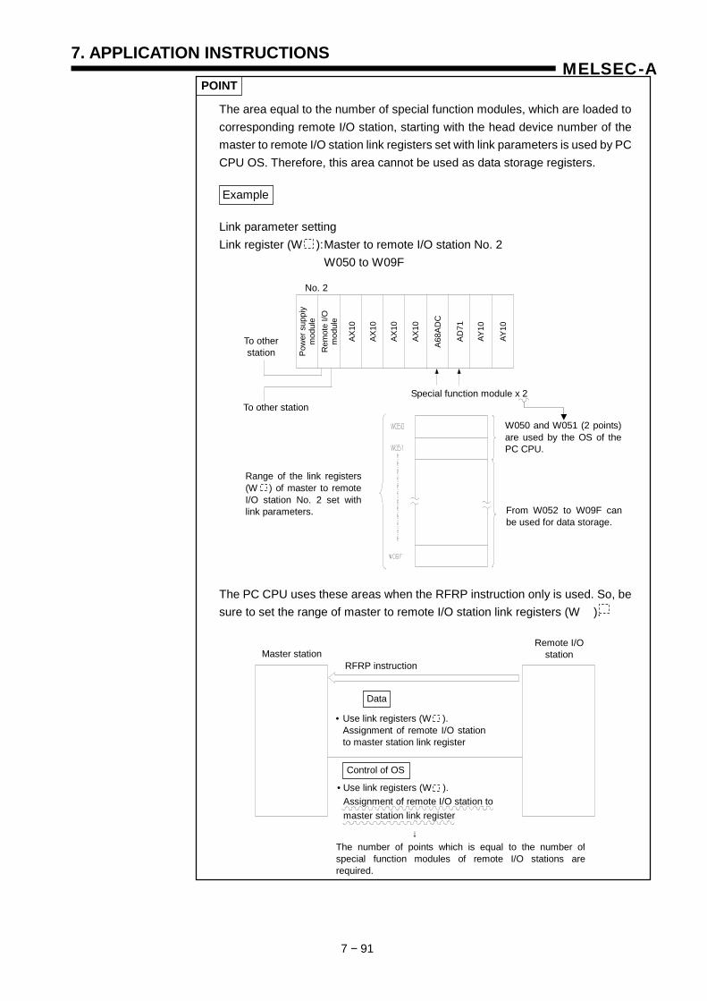
7. APPLICATION INSTRUCTIONS
7 − 91
MELSEC-APOINT
The area equal to the number of special function modules, which are loaded to corresponding remote I/O station, starting with the head device number of the master to remote I/O station link registers set with link parameters is used by PC CPU OS. Therefore, this area cannot be used as data storage registers.
Example
Link parameter setting Link register (W ): Master to remote I/O station No. 2 W050 to W09F
The PC CPU uses these areas when the RFRP instruction only is used. So, be sure to set the range of master to remote I/O station link registers (W ).
Master stationRFRP instruction
Remote I/O station
Data
Control of OS
The number of points which is equal to the number of special function modules of remote I/O stations are required.
↓
• Use link registers (W ). Assignment of remote I/O station
to master station link register
• Use link registers (W ). Assignment of remote I/O station to
master station link register
No. 2
To other stationSpecial function module x 2
To other station
W050 and W051 (2 points) are used by the OS of the PC CPU.
From W052 to W09F can be used for data storage.
Range of the link registers(W ) of master to remoteI/O station No. 2 set withlink parameters.
Pow
er s
uppi
y m
odul
e R
emot
e I/O
m
odul
e
AX10
AX10
AX10
AX10
A68A
DC
AD71
AY10
AY10
7. APPLICATION INSTRUCTIONS
7 − 92
MELSEC-A
7.9 Display Instructions
(1) Display instructions are used to output ASCII codes to the output modules, to display data on the LED display on the front panel of the CPU module and to reset the annunciator.
(2) The display instructions are available in the following seven types.
Classification Instruction Symbol Ref. Page
PR 7-94 ASCII code output
PRC 7-94
LED 7-100
LEDC 7-100
LEDA 7-103 Display
LEDB 7-103
Display reset LEDR 7-105
POINT
The LEDA and LEDB instructions cannot be used with the A3A, A3U and A4U. (Their use is changed to the start command for dedicated instructions.) To perform processings equivalent to the LEDA and LEDB instructions with the A3A, A3U and A4U, edit character string data using dedicated instructions provided for the AnA, AnU before using the LED instruction.
(3) The priority of display at the LED indicator is as indicated below.
Priority: High 1) Display due to self-diagnostic error 2) Display due to CHK. 3) Display of annunciator (F) number 4) Display due to LED, LEDC, LEDA, or LEDB Low 5) BATTERY ERROR
The above priority can be changed on the A3A, A3U and A4U. For details, refer to the A2A(S1)/A3ACPU User's Manual or the A2U (S1)/A3U/ A4UCPU User’s Manual.
(4) When there is a display at the LED indicator due to 1 to 3, the execution of display instruction does not change the display. When there is a display at the LED indicator due to 5, the execution of display instruction provides the display of that display instruction.
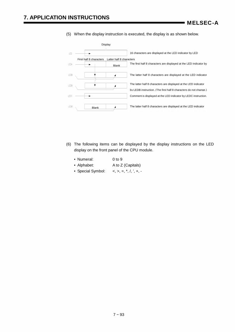
7. APPLICATION INSTRUCTIONS
7 − 93
MELSEC-A
(5) When the display instruction is executed, the display is as shown below.
(6) The following items can be displayed by the display instructions on the LED display on the front panel of the CPU module.
• Numeral: 0 to 9 • Alphabet: A to Z (Capitals) • Special Symbol: <, >, =, *, /, ’, +, -
16 characters are displayed at the LED indicator by LED
The first half 8 characters are displayed at the LED indicator by
The latter half 8 characters are displayed at the LED indicator
The latter half 8 characters are displayed at the LED indicator
by LEDB instruction. (The first half 8 characters do not change.)
Comment is displayed at the LED indicator by LEDC instruction.
The latter half 8 characters are displayed at the LED indicator
b LEDB i t ti (Th l tt h lf 8 h t bl k d )
Display
First half 8 characters Latter half 8 characters
Blank
Blank
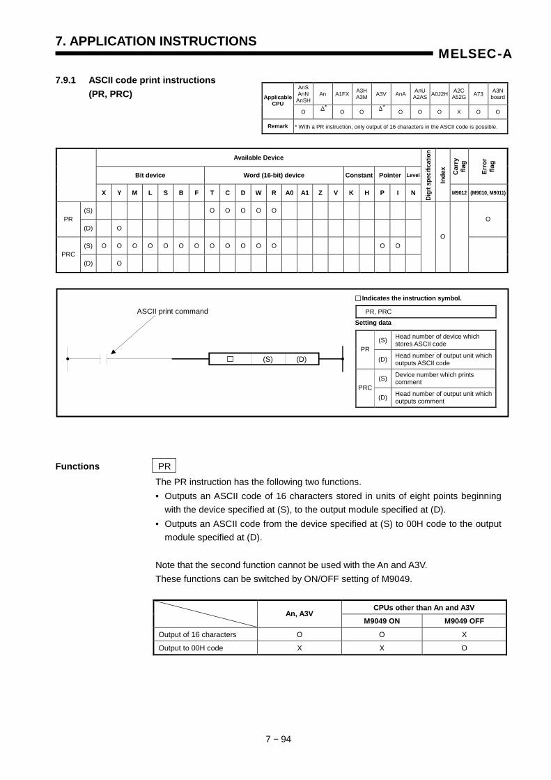
7. APPLICATION INSTRUCTIONS
7 − 94
MELSEC-A
7.9.1 ASCII code print instructions (PR, PRC)
Available Device
Bit device Word (16-bit) device Constant Pointer Level Car
ry
flag
Erro
r fla
g
X Y M L S B F T C D W R A0 A1 Z V K H P I N
Digi
t spe
cific
atio
n
Inde
x
M9012 (M9010, M9011)
(S) O O O O O PR
(D) O O
(S) O O O O O O O O O O O O O O PRC
(D) O
O
Functions PR The PR instruction has the following two functions. • Outputs an ASCII code of 16 characters stored in units of eight points beginning with the device specified at (S), to the output module specified at (D). • Outputs an ASCII code from the device specified at (S) to 00H code to the output module specified at (D). Note that the second function cannot be used with the An and A3V. These functions can be switched by ON/OFF setting of M9049.
CPUs other than An and A3V An, A3V
M9049 ON M9049 OFF
Output of 16 characters O O X
Output to 00H code X X O
AnSAnN
AnSHAn A1FX A3H
A3M A3V AnA AnU A2AS A0J2H A2C
A52G A73 A3NboardApplicable
CPU O O O O O O X O O
Remark * With a PR instruction, only output of 16 characters in the ASCII code is possible.
* *
(S) Head number of device which stores ASCII code
PR (D) Head number of output unit which
outputs ASCII code
(S) Device number which prints comment
PRC(D) Head number of output unit which
outputs comment
Setting data PR, PRC
Indicates the instruction symbol.
ASCII print command
(S) (D)
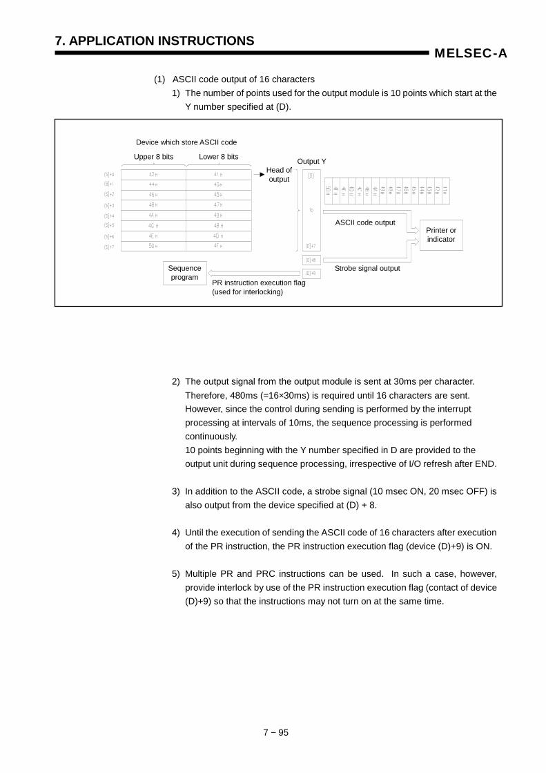
7. APPLICATION INSTRUCTIONS
7 − 95
MELSEC-A
(1) ASCII code output of 16 characters 1) The number of points used for the output module is 10 points which start at the
Y number specified at (D).
2) The output signal from the output module is sent at 30ms per character. Therefore, 480ms (=16×30ms) is required until 16 characters are sent. However, since the control during sending is performed by the interrupt processing at intervals of 10ms, the sequence processing is performed continuously. 10 points beginning with the Y number specified in D are provided to the output unit during sequence processing, irrespective of I/O refresh after END.
3) In addition to the ASCII code, a strobe signal (10 msec ON, 20 msec OFF) is
also output from the device specified at (D) + 8. 4) Until the execution of sending the ASCII code of 16 characters after execution
of the PR instruction, the PR instruction execution flag (device (D)+9) is ON. 5) Multiple PR and PRC instructions can be used. In such a case, however,
provide interlock by use of the PR instruction execution flag (contact of device (D)+9) so that the instructions may not turn on at the same time.
Device which store ASCII code
PR instruction execution flag(used for interlocking)
Sequence program
Output Y
Strobe signal output
ASCII code output Printer orindicator
Head of output
Upper 8 bits Lower 8 bits
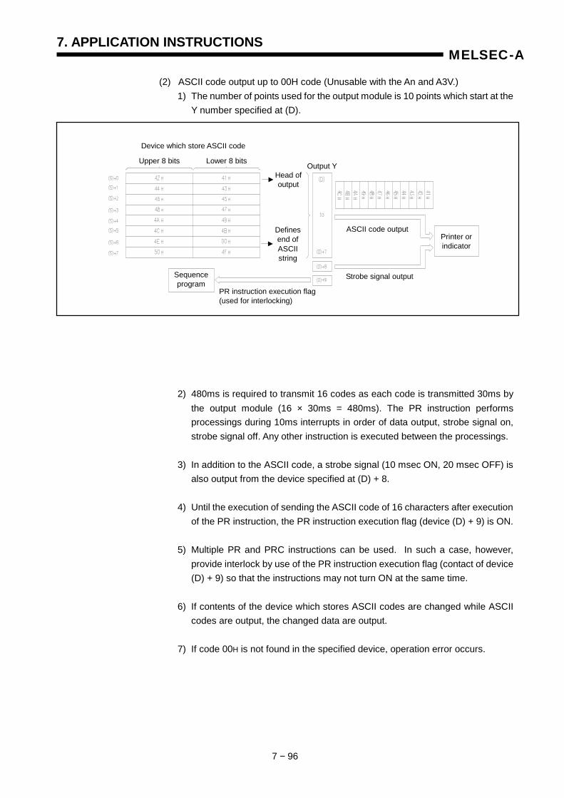
7. APPLICATION INSTRUCTIONS
7 − 96
MELSEC-A
(2) ASCII code output up to 00H code (Unusable with the An and A3V.) 1) The number of points used for the output module is 10 points which start at the
Y number specified at (D).
2) 480ms is required to transmit 16 codes as each code is transmitted 30ms by the output module (16 × 30ms = 480ms). The PR instruction performs processings during 10ms interrupts in order of data output, strobe signal on, strobe signal off. Any other instruction is executed between the processings.
3) In addition to the ASCII code, a strobe signal (10 msec ON, 20 msec OFF) is
also output from the device specified at (D) + 8. 4) Until the execution of sending the ASCII code of 16 characters after execution
of the PR instruction, the PR instruction execution flag (device (D) + 9) is ON. 5) Multiple PR and PRC instructions can be used. In such a case, however,
provide interlock by use of the PR instruction execution flag (contact of device (D) + 9) so that the instructions may not turn ON at the same time.
6) If contents of the device which stores ASCII codes are changed while ASCII
codes are output, the changed data are output. 7) If code 00H is not found in the specified device, operation error occurs.
PR instruction execution flag(used for interlocking)
Sequence program
Output Y
Strobe signal output
ASCII code output Printer orindicator
Head of output
Defines end of ASCII string
Device which store ASCII code
Upper 8 bits Lower 8 bits
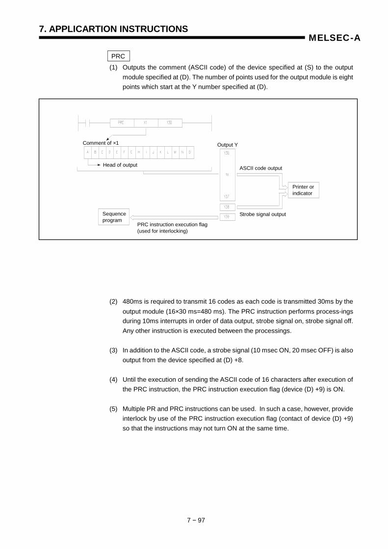
7. APPLICARTION INSTRUCTIONS
7 − 97
MELSEC-A
PRC (1) Outputs the comment (ASCII code) of the device specified at (S) to the output
module specified at (D). The number of points used for the output module is eight points which start at the Y number specified at (D).
(2) 480ms is required to transmit 16 codes as each code is transmitted 30ms by the output module (16×30 ms=480 ms). The PRC instruction performs process-ings during 10ms interrupts in order of data output, strobe signal on, strobe signal off. Any other instruction is executed between the processings.
(3) In addition to the ASCII code, a strobe signal (10 msec ON, 20 msec OFF) is also
output from the device specified at (D) +8. (4) Until the execution of sending the ASCII code of 16 characters after execution of
the PRC instruction, the PRC instruction execution flag (device (D) +9) is ON. (5) Multiple PR and PRC instructions can be used. In such a case, however, provide
interlock by use of the PRC instruction execution flag (contact of device (D) +9) so that the instructions may not turn ON at the same time.
PRC instruction execution flag (used for interlocking)
ASCII code output
Strobe signal output
Output Y
Printer or indicator
Comment of ×1
Head of output
Sequence program
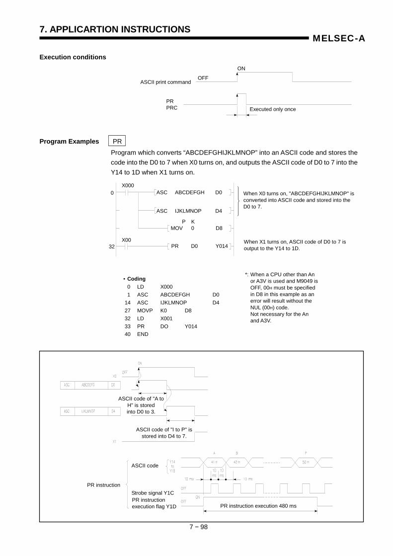
7. APPLICARTION INSTRUCTIONS
7 − 98
MELSEC-A
Execution conditions
Program Examples PR Program which converts “ABCDEFGHIJKLMNOP” into an ASCII code and stores the code into the D0 to 7 when X0 turns on, and outputs the ASCII code of D0 to 7 into the Y14 to 1D when X1 turns on.
• Coding 0 LD X000 1 ASC ABCDEFGH D0 14 ASC IJKLMNOP D4 27 MOVP K0 D8 32 LD X001 33 PR DO Y014 40 END
*: When a CPU other than An or A3V is used and M9049 is OFF, 00H must be specified in D8 in this example as an error will result without the NUL (00H) code. Not necessary for the An and A3V.
ASCII code of "A to H" is stored into D0 to 3.
ASCII code of "I to P" is stored into D4 to 7.
ASCII code
PR instruction Strobe signal Y1C PR instruction execution flag Y1D PR instruction execution 480 ms
Executed only once PR PRC
ON
OFFASCII print command
32 X00
X000 When X0 turns on, "ABCDEFGHIJKLMNOP" is converted into ASCII code and stored into the D0 to 7.
When X1 turns on, ASCII code of D0 to 7 is output to the Y14 to 1D.
ASC ABCDEFGH D0
ASC IJKLMNOP D4
P K MOV 0 D8
PR D0 Y014
0

7. APPLICARTION INSTRUCTIONS
7 − 99
MELSEC-A
PRC Program which turns on Y35, and at the same time, outputs the comment of Y35 to the Y60 to 69 when X0 turns on.
When comment of Y35 is
• Coding 0 LD X000 1 SET Y035 2 PRC Y035 Y060 9 LD X003 10 RST Y035 11 END
ASCII code
Strobe signal
PRC instruction execution flag PRC instruction execution
When X0 turns on, Y35 is turned on and comment of Y35 is output to the Y60 to 69.
X000
X003
SET Y035
PRC Y035 Y060
RST Y035
0
9
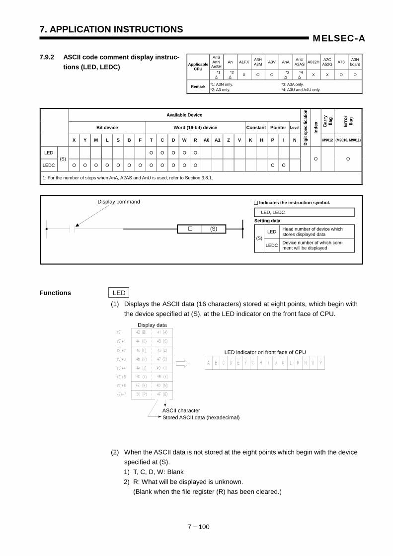
7. APPLICATION INSTRUCTIONS
7 − 100
MELSEC-A
7.9.2 ASCII code comment display instruc- tions (LED, LEDC)
Available Device
Bit device Word (16-bit) device Constant Pointer Level Car
ry
flag
Erro
r fla
g
X Y M L S B F T C D W R A0 A1 Z V K H P I N
Digi
t spe
cific
atio
n
Inde
x
M9012 (M9010, M9011)
LED O O O O O
LEDC (S)
O O O O O O O O O O O O O O O O
1: For the number of steps when AnA, A2AS and AnU is used, refer to Section 3.8.1.
Functions LED (1) Displays the ASCII data (16 characters) stored at eight points, which begin with
the device specified at (S), at the LED indicator on the front face of CPU.
(2) When the ASCII data is not stored at the eight points which begin with the device specified at (S). 1) T, C, D, W: Blank 2) R: What will be displayed is unknown. (Blank when the file register (R) has been cleared.)
AnSAnN
AnSHAn A1FX A3H
A3M A3V AnA AnU A2AS A0J2H A2C
A52G A73 A3NboardApplicable
CPU X O O X X O O
Remark *1: A3N only. *3: A3A only. *2: A3 only. *4: A3U and A4U only.
*1 *2 *3 *4
LED, LEDC
Indicates the instruction symbol. Display command
(S) LED Head number of device which stores displayed data
(S)LEDC Device number of which com-
ment will be displayed
Setting data
Display data
LED indicator on front face of CPU
ASCII character Stored ASCII data (hexadecimal)
7. APPLICATION INSTRUCTIONS
7 − 101
MELSEC-A
(3) For ASCII characters which can be displayed, refer to (3) in the section of the
LEDC instruction. (4) For the conversion of alphanumeric characters into ASCII data in a sequence
program, use the ASC instruction.

7. APPLICATION INSTRUCTIONS
7 − 102
MELSEC-A
LEDC (1) Displays the comment (15 characters) of device specified at (S) at the LED
indicator on the front of CPU. (2) When the device specified at (S) is not annotated with a comment or when it is
specified outside the comment range, the LEDC instruction results as follows.
Specification of (S) Operation of LED
with comment Comment of device is displayed at LED indicator Inside comment
range specification Without comment Display of LED indicator is cleared.
Outside comment range specification No Processing (Display of LED indicator does not change.)
(3) If the comment contains characters which cannot be displayed on the LED
indicator, display cannot be done correctly. Characters which can be displayed are as follows.
• Numerals :0to9 • Alphabets :A to Z (capitals) • Special symbols :<, >, =, *, /, ’, +, -
Execution Conditions
Display command OFF
LED LEDC Executed
only once
ON
Executed only once
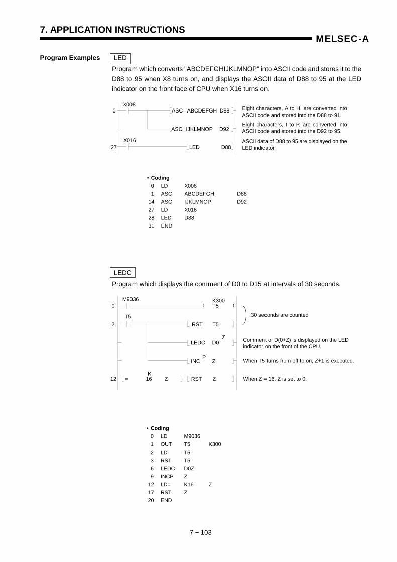
7. APPLICATION INSTRUCTIONS
7 − 103
MELSEC-A
Program Examples LED Program which converts "ABCDEFGHIJKLMNOP" into ASCII code and stores it to the D88 to 95 when X8 turns on, and displays the ASCII data of D88 to 95 at the LED indicator on the front face of CPU when X16 turns on.
LEDC Program which displays the comment of D0 to D15 at intervals of 30 seconds.
• Coding 0 LD X008 1 ASC ABCDEFGH D88 14 ASC IJKLMNOP D92 27 LD X016 28 LED D88 31 END
• Coding 0 LD M9036 1 OUT T5 K300 2 LD T5 3 RST T5 6 LEDC D0Z 9 INCP Z 12 LD= K16 Z 17 RST Z 20 END
( )
30 seconds are counted
Comment of D(0+Z) is displayed on the LED indicator on the front of the CPU.
When T5 turns from off to on, Z+1 is executed.
When Z = 16, Z is set to 0.
0 T5
2 RST T5
12 = 16 Z RST Z
M9036 K300
K
LEDC D0
INC Z P
Z
T5
Eight characters, A to H, are converted into ASCII code and stored into the D88 to 91.
Eight characters, I to P, are converted into ASCII code and stored into the D92 to 95.
ASCII data of D88 to 95 are displayed on the LED indicator.
ASC IJKLMNOP D92
X008
X016
ASC ABCDEFGH D88
LED D88
0
27
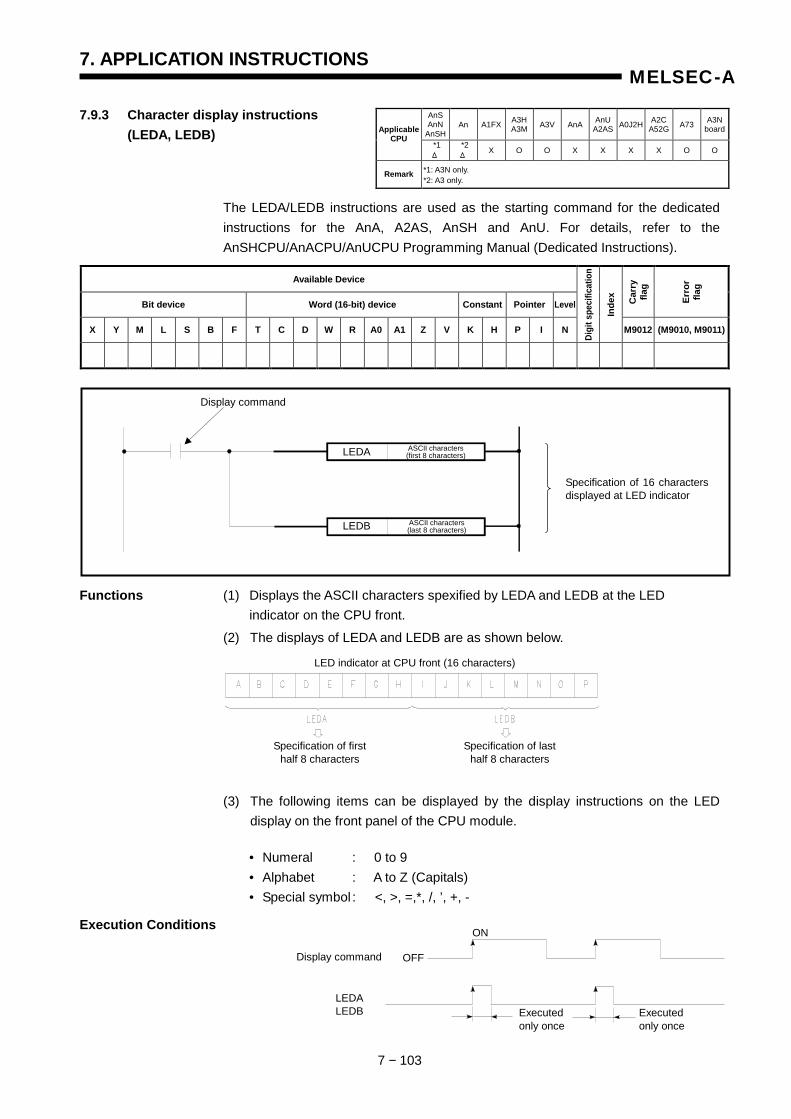
7. APPLICATION INSTRUCTIONS
7 − 103
MELSEC-A
7.9.3 Character display instructions (LEDA, LEDB)
The LEDA/LEDB instructions are used as the starting command for the dedicated instructions for the AnA, A2AS, AnSH and AnU. For details, refer to the AnSHCPU/AnACPU/AnUCPU Programming Manual (Dedicated Instructions).
Available Device
Bit device Word (16-bit) device Constant Pointer Level Car
ry
flag
Erro
r fla
g
X Y M L S B F T C D W R A0 A1 Z V K H P I N
Digi
t spe
cific
atio
n
Inde
x
M9012 (M9010, M9011)
Functions (1) Displays the ASCII characters spexified by LEDA and LEDB at the LED indicator on the CPU front.
(2) The displays of LEDA and LEDB are as shown below.
(3) The following items can be displayed by the display instructions on the LED display on the front panel of the CPU module.
• Numeral : 0 to 9 • Alphabet : A to Z (Capitals) • Special symbol : <, >, =,*, /, ’, +, -
Execution Conditions
AnSAnN
AnSHAn A1FX A3H
A3M A3V AnA AnU A2AS A0J2H A2C
A52G A73 A3NboardApplicable
CPU X O O X X X X O O
Remark *1: A3N only. *2: A3 only.
Display command
LEDA
LEDB
ASCII characters(first 8 characters)
ASCII characters(last 8 characters)
Specification of 16 charactersdisplayed at LED indicator
LED indicator at CPU front (16 characters)
Specification of first half 8 characters
Specification of last half 8 characters
*2 *1
Display command OFF
ON
Executed only once
LEDA LEDB Executed
only once
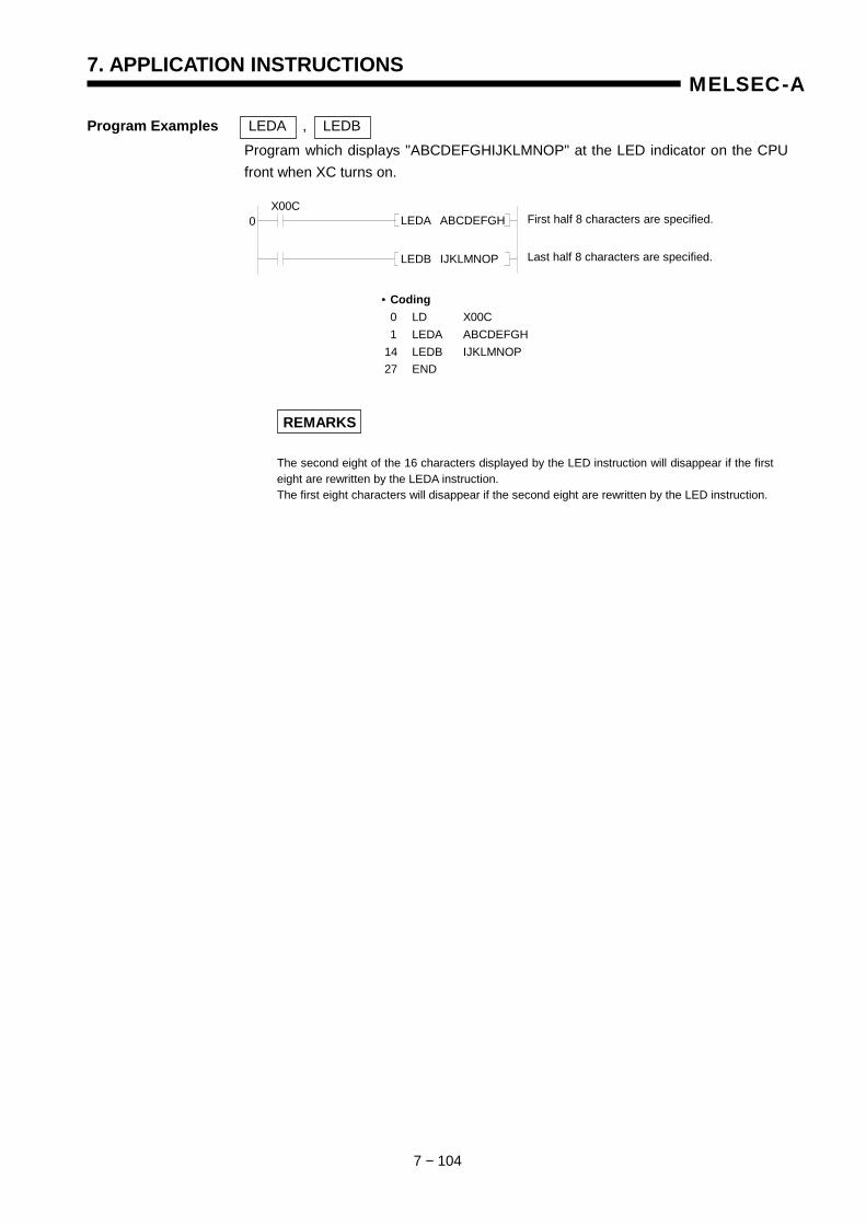
7. APPLICATION INSTRUCTIONS
7 − 104
MELSEC-A
Program Examples LEDA , LEDB Program which displays "ABCDEFGHIJKLMNOP" at the LED indicator on the CPU front when XC turns on.
REMARKS
The second eight of the 16 characters displayed by the LED instruction will disappear if the first eight are rewritten by the LEDA instruction. The first eight characters will disappear if the second eight are rewritten by the LED instruction.
• Coding 0 LD X00C 1 LEDA ABCDEFGH 14 LEDB IJKLMNOP 27 END
First half 8 characters are specified.
Last half 8 characters are specified.
0 X00C LEDA ABCDEFGH
LEDB IJKLMNOP
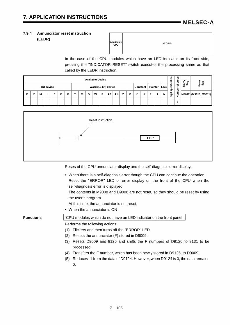
7. APPLICATION INSTRUCTIONS
7 − 105
MELSEC-A
7.9.4 Annunciator reset instruction (LEDR)
In the case of the CPU modules which have an LED indicator on its front side, pressing the "INDICATOR RESET" switch executes the processing same as that called by the LEDR instruction.
Available Device
Bit device Word (16-bit) device Constant Pointer Level Car
ry
flag
Erro
r fla
g
X Y M L S B F T C D W R A0 A1 Z V K H P I N
Digi
t spe
cific
atio
n
Num
ber o
f ste
ps
M9012 (M9010, M9011)
1
Reses of the CPU annunciator display and the self-diagnosis error display.
• When there is a self-diagnosis error though the CPU can continue the operation. Reset the "ERROR" LED or error display on the front of the CPU when the self-diagnosis error is displayed. The contents in M9008 and D9008 are not reset, so they should be reset by using the user’s program.
At this time, the annunciator is not reset. • When the annunciator is ON
Functions CPU modules which do not have an LED indicator on the front panel Performs the following actions: (1) Flickers and then turns off the "ERROR" LED. (2) Resets the annunciator (F) stored in D9009. (3) Resets D9009 and 9125 and shifts the F numbers of D9126 to 9131 to be
processed. (4) Transfers the F number, which has been newly stored in D9125, to D9009. (5) Reduces -1 from the data of D9124. However, when D9124 is 0, the data remains
0.
Applicable CPU All CPUs
Reset instruction
LEDR
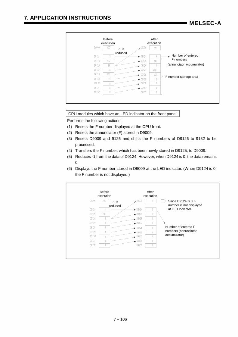
7. APPLICATION INSTRUCTIONS
7 − 106
MELSEC-A
CPU modules which have an LED indicator on the front panel Performs the following actions: (1) Resets the F number displayed at the CPU front. (2) Resets the annunciator (F) stored in D9009. (3) Resets D9009 and 9125 and shifts the F numbers of D9126 to 9132 to be
processed. (4) Transfers the F number, which has been newly stored in D9125, to D9009. (5) Reduces -1 from the data of D9124. However, when D9124 is 0, the data remains
0. (6) Displays the F number stored in D9009 at the LED indicator. (When D9124 is 0,
the F number is not displayed.)
Number of entered F numbers
F number storage area
(annunciaor accumulator)
Before execution
After execution
-1 isreduced
Since D9124 is 0, F number is not displayed at LED indicator.
Number of entered F numbers (annunciator accumulator)
Before execution
After execution
-1 is reduced
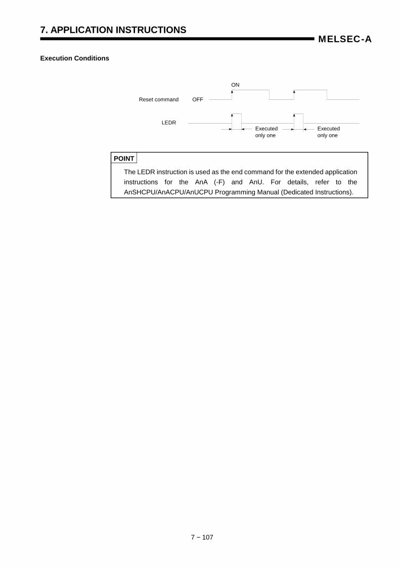
7. APPLICATION INSTRUCTIONS
7 − 107
MELSEC-A
Execution Conditions
POINT
The LEDR instruction is used as the end command for the extended application instructions for the AnA (-F) and AnU. For details, refer to the AnSHCPU/AnACPU/AnUCPU Programming Manual (Dedicated Instructions).
Reset command OFF
ON
LEDR Executed only one
Executed only one
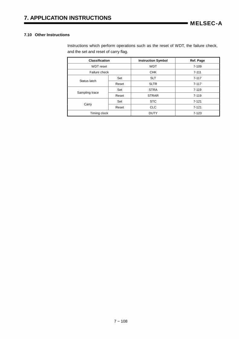
7. APPLICATION INSTRUCTIONS
7 − 108
MELSEC-A
7.10 Other Instructions
Instructions which perform operations such as the reset of WDT, the failure check, and the set and reset of carry flag.
Classification Instruction Symbol Ref. Page
WDT reset WDT 7-109
Failure check CHK 7-111
Set SLT 7-117 Status latch
Reset SLTR 7-117
Set STRA 7-119 Sampling trace
Reset STRAR 7-119
Set STC 7-121 Carry
Reset CLC 7-121
Timing clock DUTY 7-123
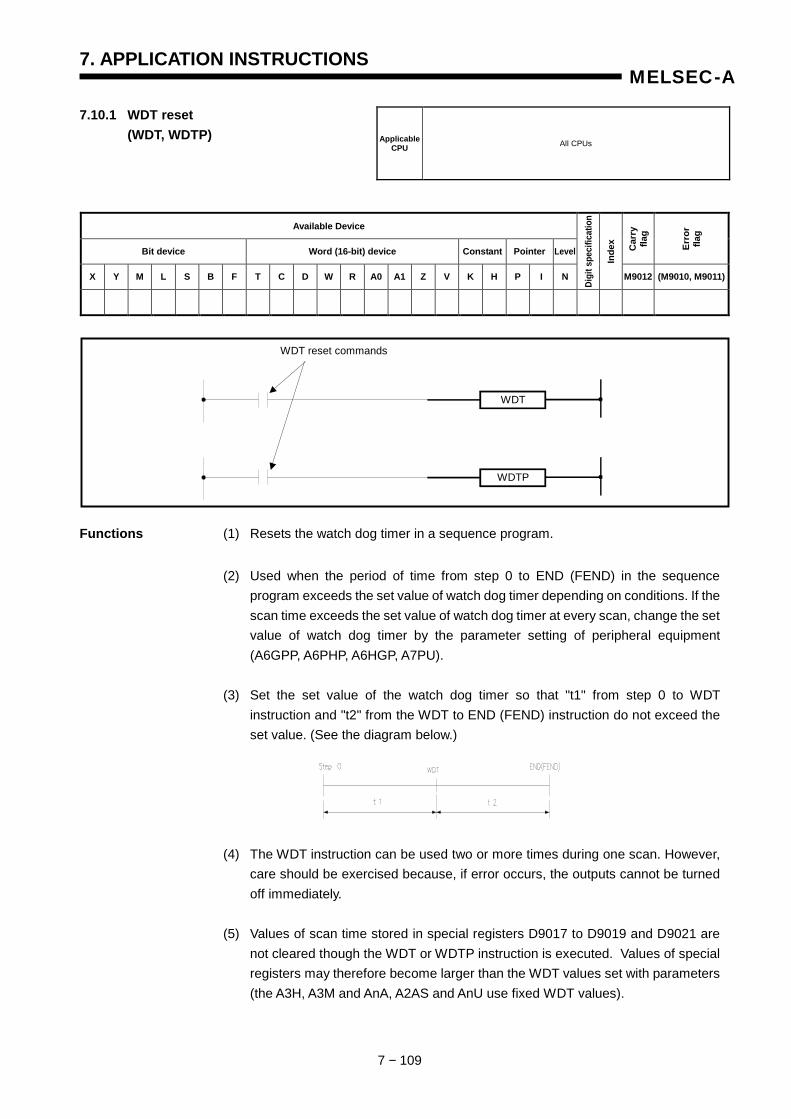
7. APPLICATION INSTRUCTIONS
7 − 109
MELSEC-A
7.10.1 WDT reset (WDT, WDTP)
Available Device
Bit device Word (16-bit) device Constant Pointer Level Car
ry
flag
Erro
r fla
g
X Y M L S B F T C D W R A0 A1 Z V K H P I N
Digi
t spe
cific
atio
n
Inde
x
M9012 (M9010, M9011)
Functions (1) Resets the watch dog timer in a sequence program. (2) Used when the period of time from step 0 to END (FEND) in the sequence
program exceeds the set value of watch dog timer depending on conditions. If the scan time exceeds the set value of watch dog timer at every scan, change the set value of watch dog timer by the parameter setting of peripheral equipment (A6GPP, A6PHP, A6HGP, A7PU).
(3) Set the set value of the watch dog timer so that "t1" from step 0 to WDT
instruction and "t2" from the WDT to END (FEND) instruction do not exceed the set value. (See the diagram below.)
(4) The WDT instruction can be used two or more times during one scan. However, care should be exercised because, if error occurs, the outputs cannot be turned off immediately.
(5) Values of scan time stored in special registers D9017 to D9019 and D9021 are
not cleared though the WDT or WDTP instruction is executed. Values of special registers may therefore become larger than the WDT values set with parameters (the A3H, A3M and AnA, A2AS and AnU use fixed WDT values).
Applicable CPU All CPUs
WDT
WDTP
WDT reset commands
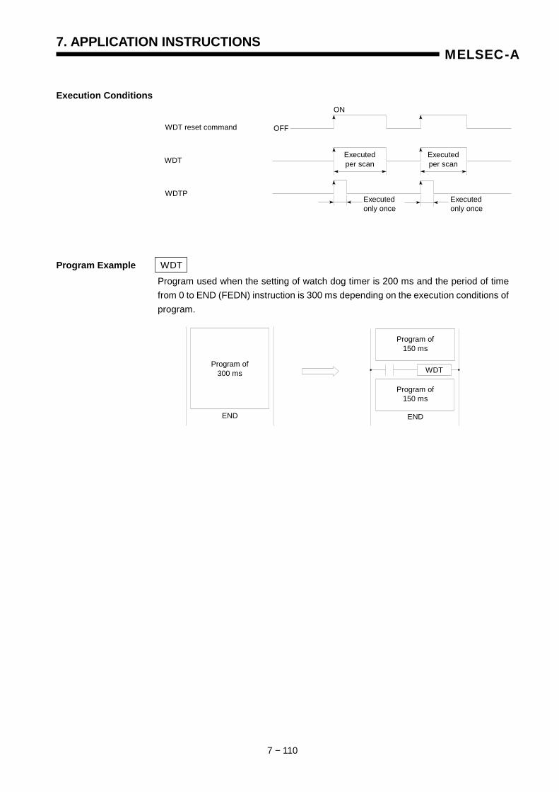
7. APPLICATION INSTRUCTIONS
7 − 110
MELSEC-A
Execution Conditions
Program Example WDT Program used when the setting of watch dog timer is 200 ms and the period of time from 0 to END (FEDN) instruction is 300 ms depending on the execution conditions of program.
OFF
ON
Executed per scan
Executed per scan
Executed only once
Executed only once
WDT
WDTP
WDT reset command
Program of 300 ms
Program of 150 ms
Program of 150 ms
WDT
END END
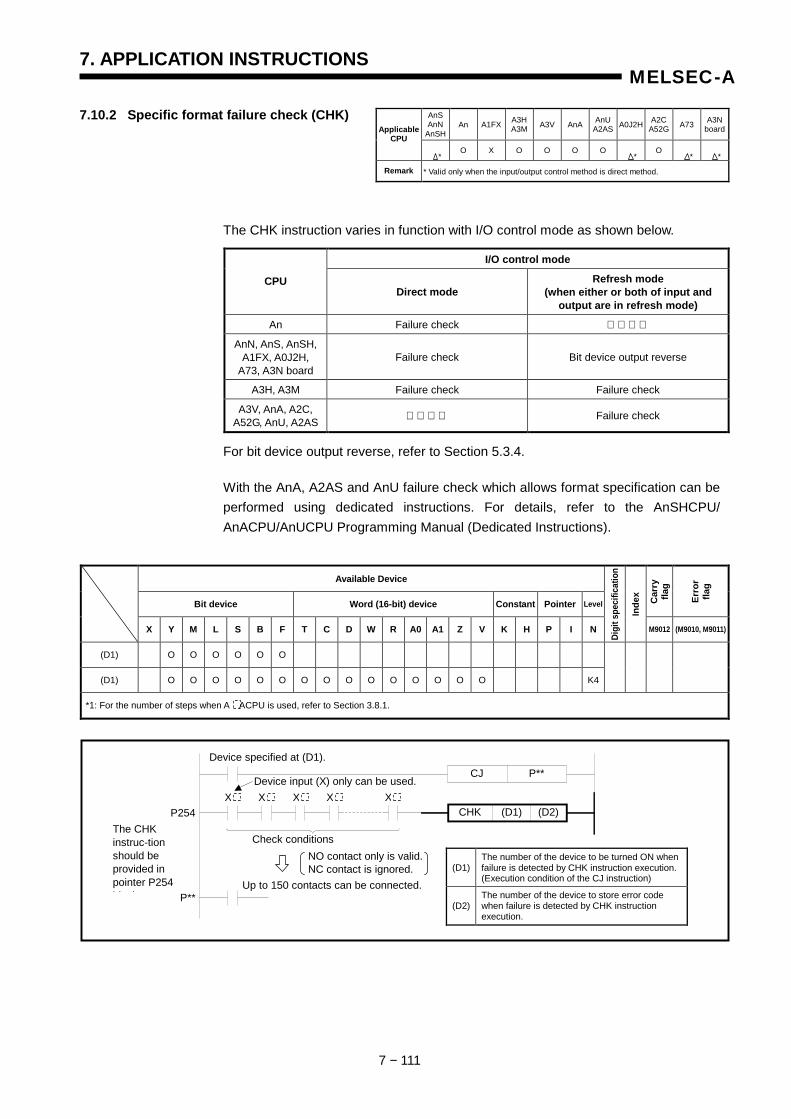
7. APPLICATION INSTRUCTIONS
7 − 111
MELSEC-A
7.10.2 Specific format failure check (CHK)
The CHK instruction varies in function with I/O control mode as shown below.
I/O control mode
CPU Direct mode
Refresh mode (when either or both of input and
output are in refresh mode)
An Failure check
AnN, AnS, AnSH, A1FX, A0J2H,
A73, A3N board Failure check Bit device output reverse
A3H, A3M Failure check Failure check
A3V, AnA, A2C, A52G, AnU, A2AS Failure check
For bit device output reverse, refer to Section 5.3.4.
With the AnA, A2AS and AnU failure check which allows format specification can be performed using dedicated instructions. For details, refer to the AnSHCPU/ AnACPU/AnUCPU Programming Manual (Dedicated Instructions).
Available Device
Bit device Word (16-bit) device Constant Pointer Level Car
ry
flag
Erro
r fla
g
X Y M L S B F T C D W R A0 A1 Z V K H P I N Di
git s
peci
ficat
ion
Inde
x M9012 (M9010, M9011)
(D1) O O O O O O
(D1) O O O O O O O O O O O O O O O K4
*1: For the number of steps when A ACPU is used, refer to Section 3.8.1.
AnSAnN
AnSHAn A1FX A3H
A3M A3V AnA AnU A2AS A0J2H A2C
A52G A73 A3NboardApplicable
CPU O X O O O O O
Remark * Valid only when the input/output control method is direct method.
Device specified at (D1).
Device input (X) only can be used.
Up to 150 contacts can be connected.
NO contact only is valid. NC contact is ignored.
Check conditions The CHK instruc-tion should be provided in pointer P254 bl k
CJ P**
CHK (D1) (D2)X X X X X
P254
P**
(D1) The number of the device to be turned ON when failure is detected by CHK instruction execution. (Execution condition of the CJ instruction)
(D2) The number of the device to store error code when failure is detected by CHK instruction execution.
* * * *
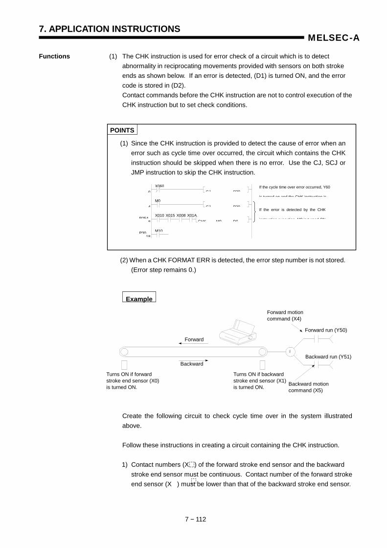
7. APPLICATION INSTRUCTIONS
7 − 112
MELSEC-A
Functions (1) The CHK instruction is used for error check of a circuit which is to detect abnormality in reciprocating movements provided with sensors on both stroke ends as shown below. If an error is detected, (D1) is turned ON, and the error code is stored in (D2).
Contact commands before the CHK instruction are not to control execution of the CHK instruction but to set check conditions.
POINTS
(1) Since the CHK instruction is provided to detect the cause of error when an error such as cycle time over occurred, the circuit which contains the CHK instruction should be skipped when there is no error. Use the CJ, SCJ or JMP instruction to skip the CHK instruction.
(2) When a CHK FORMAT ERR is detected, the error step number is not stored.
(Error step remains 0.)
Example
Create the following circuit to check cycle time over in the system illustrated above.
Follow these instructions in creating a circuit containing the CHK instruction.
1) Contact numbers (X ) of the forward stroke end sensor and the backward
stroke end sensor must be continuous. Contact number of the forward stroke end sensor (X ) must be lower than that of the backward stroke end sensor.
X060
M0
X010
M10
X015 X008 X01A
0
4
8
18
P254
P30
CJ P30
CJ P30
CHK M0 D0
If the cycle time over error occurred, Y60
is turned on and the CHK instruction is
If the error is detected by the CHK
instruction execution M0 is turned ON
Forward motion command (X4)
Forward run (Y50)
Backward run (Y51)
Backward motion command (X5)
Turns ON if backward stroke end sensor (X1) is turned ON.
Turns ON if forward stroke end sensor (X0) is turned ON.
Forward
Backward
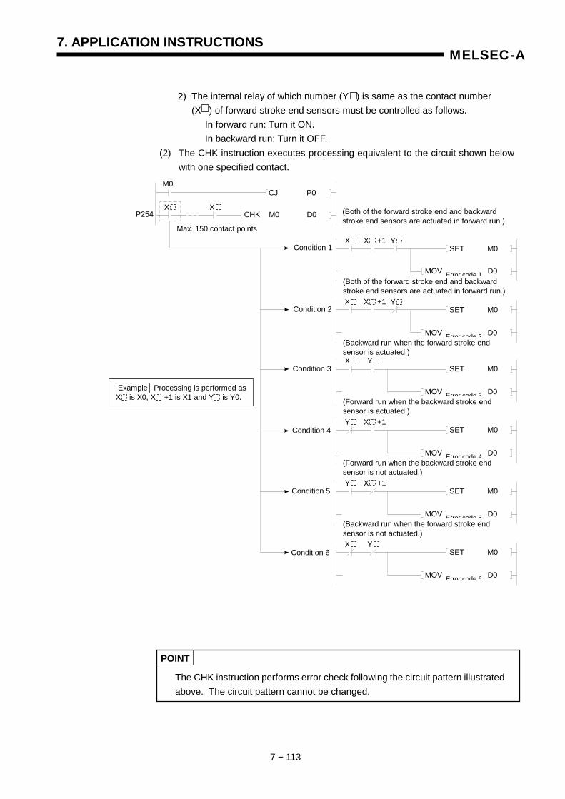
7. APPLICATION INSTRUCTIONS
7 − 113
MELSEC-A
2) The internal relay of which number (Y ) is same as the contact number
(X ) of forward stroke end sensors must be controlled as follows. In forward run: Turn it ON. In backward run: Turn it OFF.
(2) The CHK instruction executes processing equivalent to the circuit shown below with one specified contact.
POINT
The CHK instruction performs error check following the circuit pattern illustrated above. The circuit pattern cannot be changed.
M0
X Y
X X
CJ P0
CHK M0 D0
Max. 150 contact points
(Both of the forward stroke end and backward stroke end sensors are actuated in forward run.)
Condition 1
Condition 2
Condition 3
Condition 4
Condition 5
Condition 6
X +1SET M0
MOV D0 Error code 1(Both of the forward stroke end and backward stroke end sensors are actuated in forward run.)X YX +1
SET M0
MOV D0 Error code 2(Backward run when the forward stroke end sensor is actuated.) X Y
SET M0
MOV D0 Error code 3(Forward run when the backward stroke end sensor is actuated.) Y X +1
SET M0
MOV D0 Error code 4(Forward run when the backward stroke end sensor is not actuated.) Y X +1
SET M0
MOV D0 Error code 5(Backward run when the forward stroke end sensor is not actuated.) X Y
SET M0
MOV D0 Error code 6
Example Processing is performed asX is X0, X +1 is X1 and Y is Y0.
P254

7. APPLICATION INSTRUCTIONS
7 − 117
MELSEC-A
7.10.3 Status latch set, reset (SLT, SLTR)
Available Device
Bit device Word (16-bit) device Constant Pointer Level Car
ry
flag
Erro
r fla
g
X Y M L S B F T C D W R A0 A1 Z V K H P I N
Digi
t spe
cific
atio
n
Inde
x
M9012 (M9010, M9011)
Functions SLT (1) When executed, the SLT instruction stores the contents of data memories and file
registers set by the parameter setting of peripheral unit A6GPP, A6PHP, A6HGP into the memory for status latch in the user memory area.
(2) Status latch is allowed for the following devices. Data memory: ON/OFF displays of X, Y, M, B, and F Present values of T and C Contents of D, W, A0, A1, Z and V Contents of file registers (3) When the SLT instruction is executed only once. (4) The result of status latch can be monitored by the A6GPP, A6PHP, A6HGP.
SLTR (1) A reset instruction of SLT instruction. (2) By executing the SLTR instruction, the SLT instruction is enabled again.
SLT
SLTR
Execution of status latch
Reset of status latch
Status latch command
Reset command
AnSAnN
AnSHAn A1FX A3H
A3M A3V AnA AnU A2AS A0J2H A2C
A52G A73 A3NboardApplicable
CPU O O O O O O O O O
Remark *1: Unusable with A1N. *2: Unusable with A1.
*1 *2
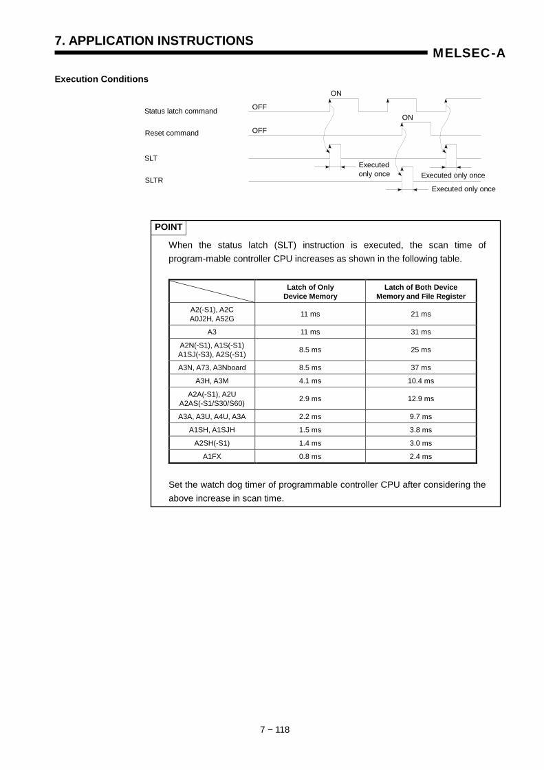
7. APPLICATION INSTRUCTIONS
7 − 118
MELSEC-A
Execution Conditions
POINT
When the status latch (SLT) instruction is executed, the scan time of program-mable controller CPU increases as shown in the following table.
Latch of Only Device Memory
Latch of Both Device Memory and File Register
A2(-S1), A2C A0J2H, A52G 11 ms 21 ms
A3 11 ms 31 ms
A2N(-S1), A1S(-S1) A1SJ(-S3), A2S(-S1) 8.5 ms 25 ms
A3N, A73, A3Nboard 8.5 ms 37 ms
A3H, A3M 4.1 ms 10.4 ms
A2A(-S1), A2U A2AS(-S1/S30/S60) 2.9 ms 12.9 ms
A3A, A3U, A4U, A3A 2.2 ms 9.7 ms
A1SH, A1SJH 1.5 ms 3.8 ms
A2SH(-S1) 1.4 ms 3.0 ms
A1FX 0.8 ms 2.4 ms
Set the watch dog timer of programmable controller CPU after considering the above increase in scan time.
OFF
ON
Executed only once Executed only once
Status latch command
OFF
ON
Executed only once
Reset command
SLT
SLTR
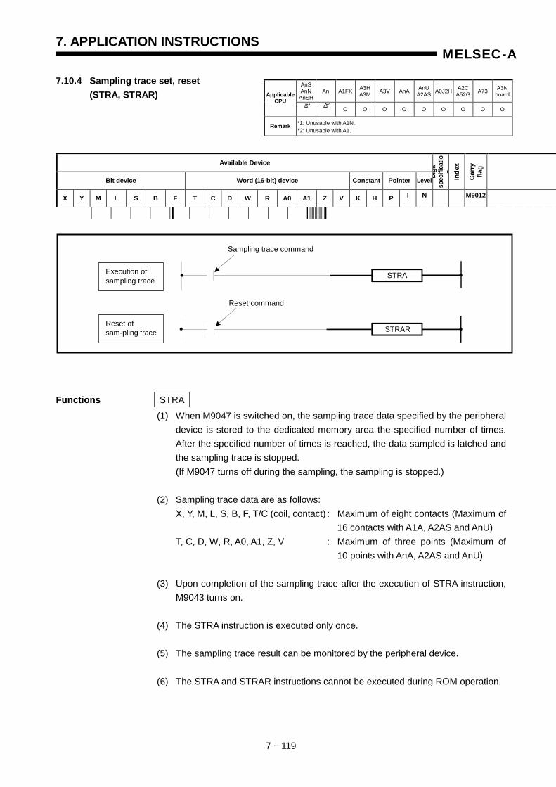
7. APPLICATION INSTRUCTIONS
7 − 119
MELSEC-A
7.10.4 Sampling trace set, reset (STRA, STRAR)
Available Device
Bit device Word (16-bit) device Constant Pointer Level Digi
t sp
ecifi
catio
nIn
dex
Car
ry
flag
X Y M L S B F T C D W R A0 A1 Z V K H P I N M9012
Functions STRA (1) When M9047 is switched on, the sampling trace data specified by the peripheral
device is stored to the dedicated memory area the specified number of times. After the specified number of times is reached, the data sampled is latched and the sampling trace is stopped.
(If M9047 turns off during the sampling, the sampling is stopped.) (2) Sampling trace data are as follows: X, Y, M, L, S, B, F, T/C (coil, contact) : Maximum of eight contacts (Maximum of
16 contacts with A1A, A2AS and AnU) T, C, D, W, R, A0, A1, Z, V : Maximum of three points (Maximum of
10 points with AnA, A2AS and AnU) (3) Upon completion of the sampling trace after the execution of STRA instruction,
M9043 turns on. (4) The STRA instruction is executed only once. (5) The sampling trace result can be monitored by the peripheral device. (6) The STRA and STRAR instructions cannot be executed during ROM operation.
AnSAnN
AnSHAn A1FX A3H
A3M A3V AnA AnU A2AS A0J2H A2C
A52G A73 A3NboardApplicable
CPU O O O O O O O O O
Remark *1: Unusable with A1N. *2: Unusable with A1.
*1 *2
STRA
STRAR
Execution of sampling trace
Reset of sam-pling trace
Sampling trace command
Reset command

7. APPLICATION INSTRUCTIONS
7 − 120
MELSEC-A
STRAR (1) Reset instruction for the STRA instruction. (2) By executing the STRAR instruction, the STRA instruction is enabled again. (3) Turns off M9043.
Execution Conditions
OFF
ON
Executed only once Executed only once
Sampling trace command
OFF
ON
Executed only once
Reset command
STRA
STRAR
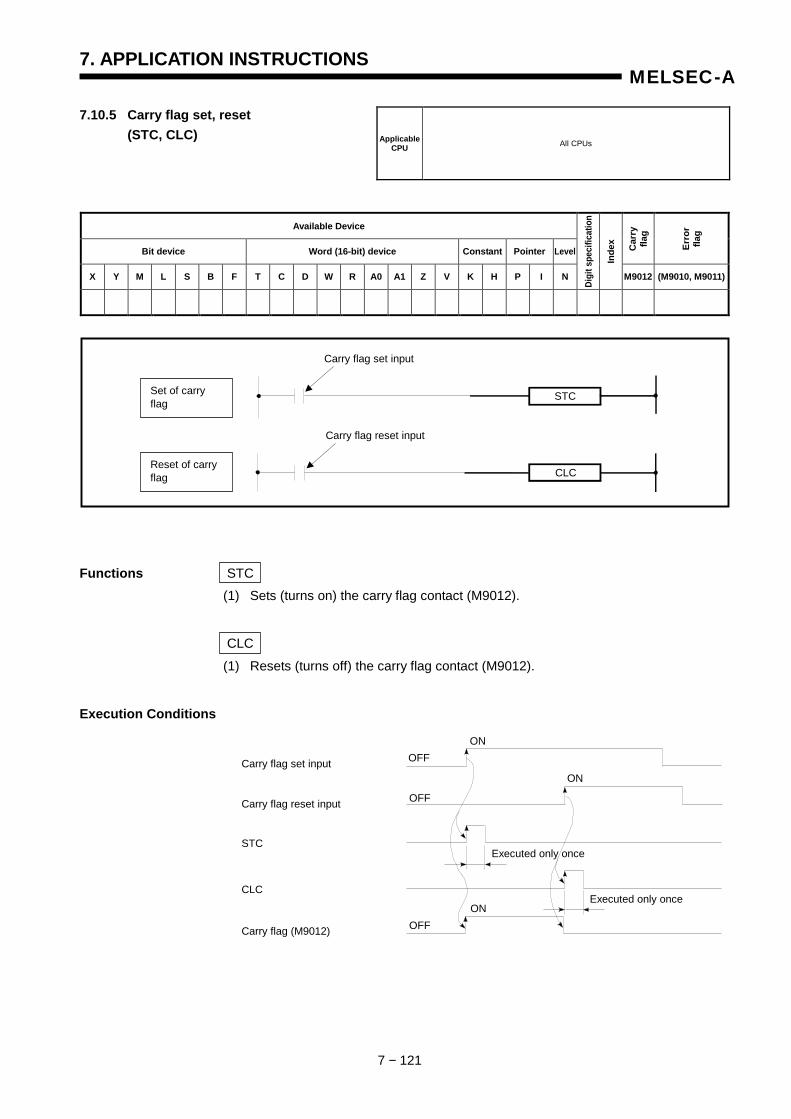
7. APPLICATION INSTRUCTIONS
7 − 121
MELSEC-A
7.10.5 Carry flag set, reset (STC, CLC)
Available Device
Bit device Word (16-bit) device Constant Pointer Level Car
ry
flag
Erro
r fla
g
X Y M L S B F T C D W R A0 A1 Z V K H P I N
Digi
t spe
cific
atio
n
Inde
x
M9012 (M9010, M9011)
Functions STC (1) Sets (turns on) the carry flag contact (M9012).
CLC
(1) Resets (turns off) the carry flag contact (M9012).
Execution Conditions
Applicable CPU All CPUs
STC
CLC
Set of carry flag
Reset of carry flag
Carry flag set input
Carry flag reset input
OFF ON
Executed only once
Carry flag set input
OFF
ON
Executed only once
Carry flag reset input
STC
CLC
OFF ON
Carry flag (M9012)
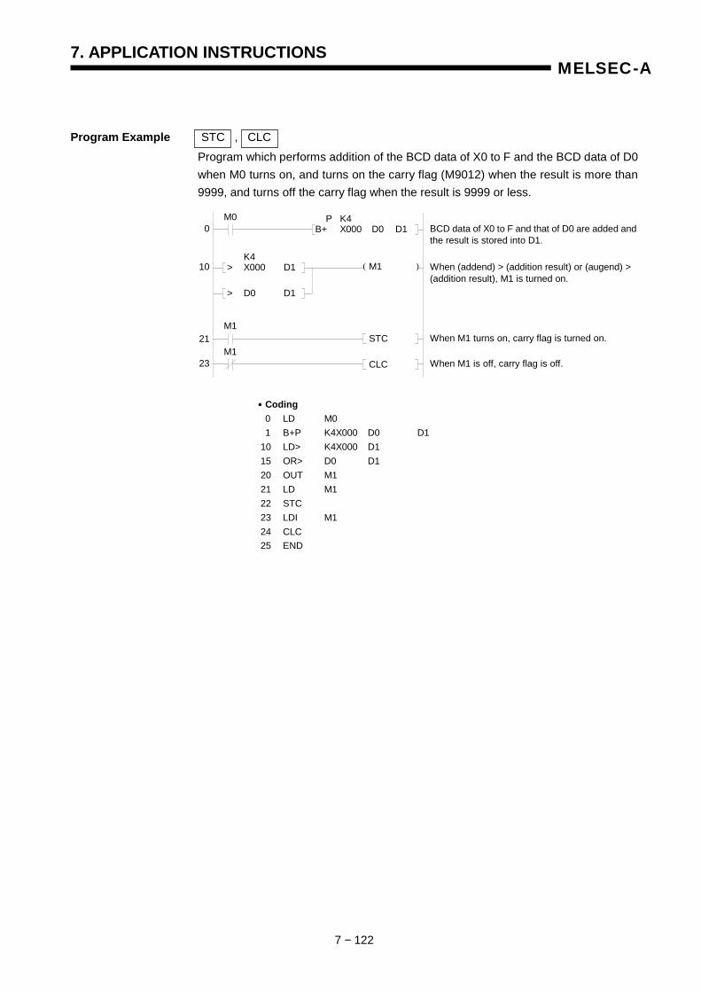
7. APPLICATION INSTRUCTIONS
7 − 122
MELSEC-A
Program Example STC , CLC
Program which performs addition of the BCD data of X0 to F and the BCD data of D0 when M0 turns on, and turns on the carry flag (M9012) when the result is more than 9999, and turns off the carry flag when the result is 9999 or less.
( )
M0 0
P K4 B+ X000 D0 D1
K4 > X000 D1
BCD data of X0 to F and that of D0 are added and the result is stored into D1.
When (addend) > (addition result) or (augend) > (addition result), M1 is turned on.
•••• Coding 0 LD M0 1 B+P K4X000 D0 D1 10 LD> K4X000 D1 15 OR> D0 D1 20 OUT M1 21 LD M1 22 STC 23 LDI M1 24 CLC 25 END
When M1 turns on, carry flag is turned on.
M1
> D0 D1
STC
CLC
10
21
23
M1
M1 When M1 is off, carry flag is off.
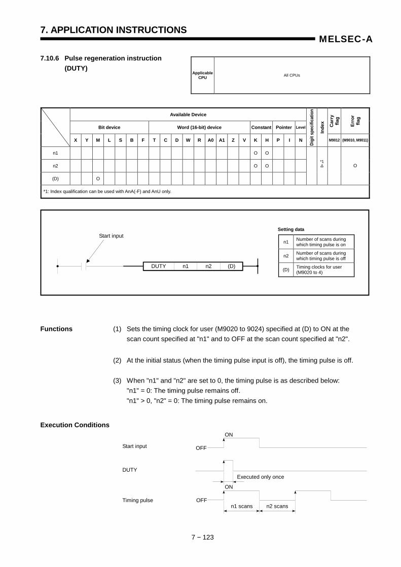
7. APPLICATION INSTRUCTIONS
7 − 123
MELSEC-A
7.10.6 Pulse regeneration instruction (DUTY)
Available Device
Bit device Word (16-bit) device Constant Pointer Level Car
ry
flag
Erro
r fla
g
X Y M L S B F T C D W R A0 A1 Z V K H P I N
Digi
t spe
cific
atio
n
Inde
x
M9012 (M9010, M9011)
n1 O O
n2 O O
(D) O
O
*1: Index qualification can be used with AnA(-F) and AnU only.
Functions (1) Sets the timing clock for user (M9020 to 9024) specified at (D) to ON at the scan count specified at "n1" and to OFF at the scan count specified at "n2".
(2) At the initial status (when the timing pulse input is off), the timing pulse is off. (3) When "n1" and "n2" are set to 0, the timing pulse is as described below: "n1" = 0: The timing pulse remains off. "n1" > 0, "n2" = 0: The timing pulse remains on.
Execution Conditions
Applicable CPU All CPUs
*1
DUTY
Start input
n1 n2 (D)
n1 Number of scans during which timing pulse is on
n2 Number of scans during which timing pulse is off
(D) Timing clocks for user (M9020 to 4)
Setting data
OFF
ON
Executed only once
Start input
OFF
ON
DUTY
Timing pulse n1 scans n2 scans
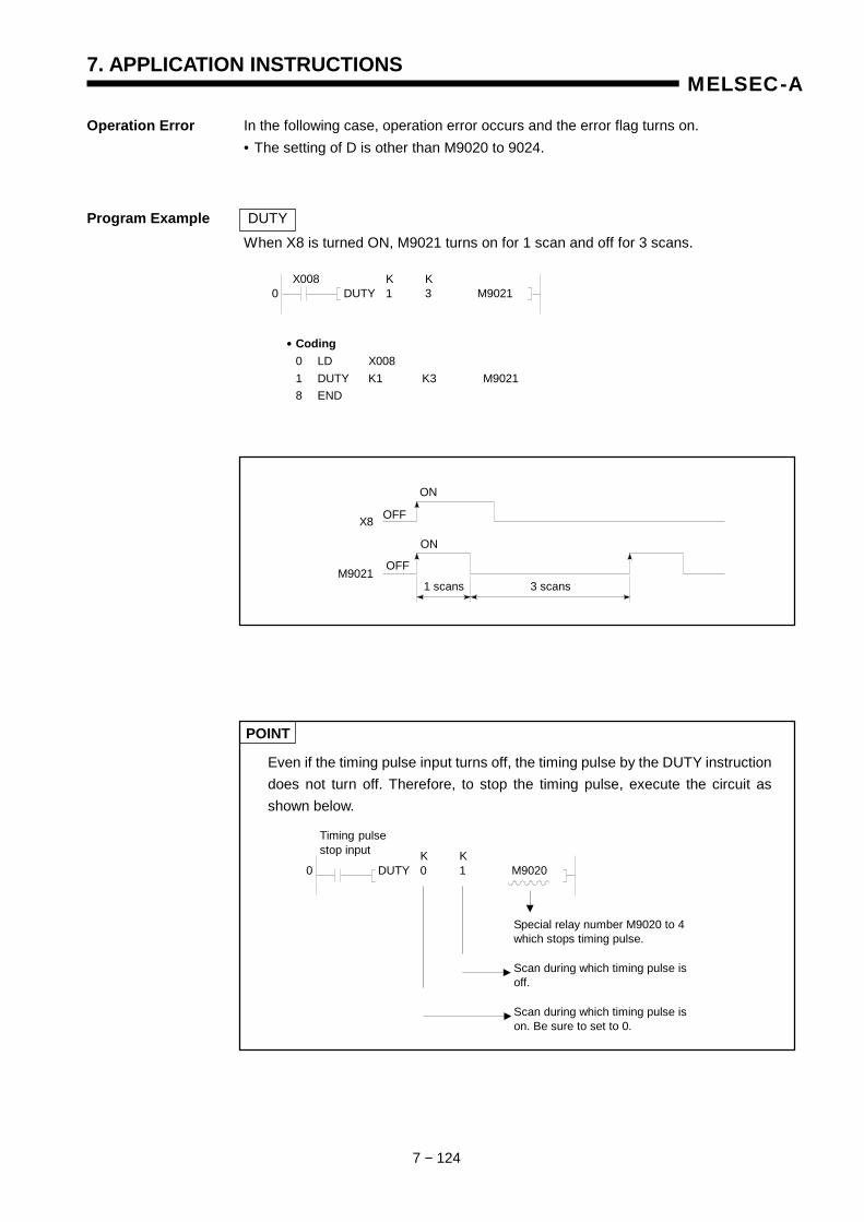
7. APPLICATION INSTRUCTIONS
7 − 124
MELSEC-A
Operation Error In the following case, operation error occurs and the error flag turns on. • The setting of D is other than M9020 to 9024.
Program Example DUTY When X8 is turned ON, M9021 turns on for 1 scan and off for 3 scans.
POINT
Even if the timing pulse input turns off, the timing pulse by the DUTY instruction does not turn off. Therefore, to stop the timing pulse, execute the circuit as shown below.
0 X008 K K
DUTY 1 3 M9021
•••• Coding 0 LD X008 1 DUTY K1 K3 M9021 8 END
OFF
ON
X8
OFF
ON
M90211 scans 3 scans
0
Timing pulsestop input K K
DUTY 0 1 M9020
Special relay number M9020 to 4 which stops timing pulse.
Scan during which timing pulse is off.
Scan during which timing pulse is on. Be sure to set to 0.
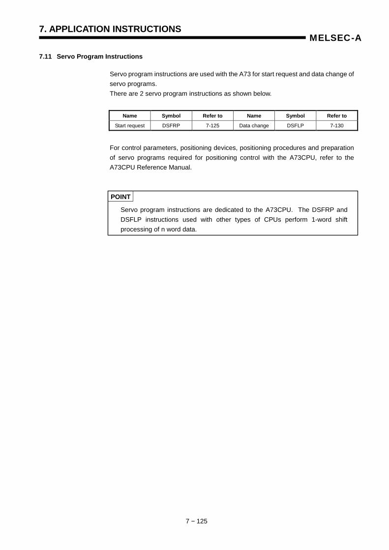
7. APPLICATION INSTRUCTIONS
7 − 125
MELSEC-A
7.11 Servo Program Instructions
Servo program instructions are used with the A73 for start request and data change of servo programs. There are 2 servo program instructions as shown below.
Name Symbol Refer to Name Symbol Refer to
Start request DSFRP 7-125 Data change DSFLP 7-130
For control parameters, positioning devices, positioning procedures and preparation of servo programs required for positioning control with the A73CPU, refer to the A73CPU Reference Manual.
POINT
Servo program instructions are dedicated to the A73CPU. The DSFRP and DSFLP instructions used with other types of CPUs perform 1-word shift processing of n word data.
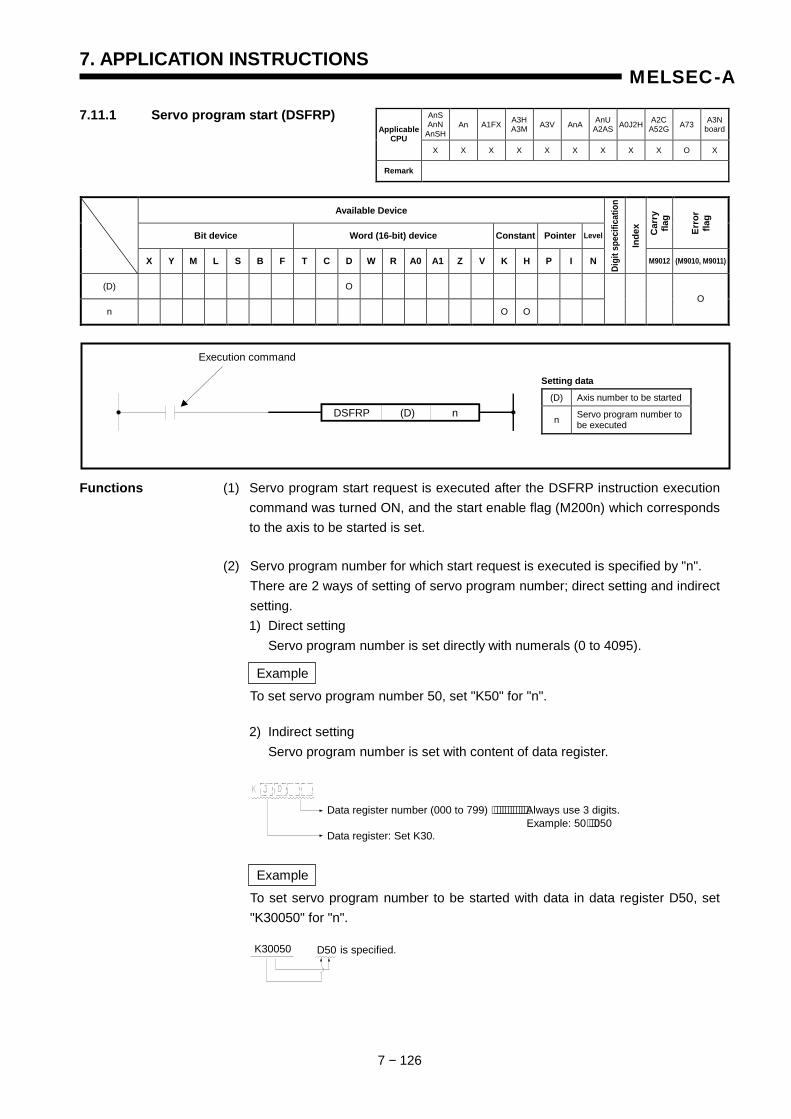
7. APPLICATION INSTRUCTIONS
7 − 126
MELSEC-A
7.11.1 Servo program start (DSFRP)
Available Device
Bit device Word (16-bit) device Constant Pointer Level Car
ry
flag
Erro
r fla
g
X Y M L S B F T C D W R A0 A1 Z V K H P I N
Digi
t spe
cific
atio
n
Inde
x
M9012 (M9010, M9011)
(D) O
n O O O
Functions (1) Servo program start request is executed after the DSFRP instruction execution command was turned ON, and the start enable flag (M200n) which corresponds to the axis to be started is set.
(2) Servo program number for which start request is executed is specified by "n". There are 2 ways of setting of servo program number; direct setting and indirect
setting. 1) Direct setting Servo program number is set directly with numerals (0 to 4095).
Example
To set servo program number 50, set "K50" for "n".
2) Indirect setting Servo program number is set with content of data register.
Example
To set servo program number to be started with data in data register D50, set "K30050" for "n".
AnSAnN
AnSHAn A1FX A3H
A3M A3V AnA AnU A2AS A0J2H A2C
A52G A73 A3NboardApplicable
CPU X X X X X X X X X O X
Remark
Execution command
DSFRP (D) n (D) Axis number to be started
n Servo program number to be executed
Setting data
Data register number (000 to 799) ⋅⋅⋅⋅⋅⋅⋅⋅⋅⋅⋅⋅⋅Always use 3 digits. Example: 50⋅⋅⋅050 Data register: Set K30.
is specified. K30050 D50
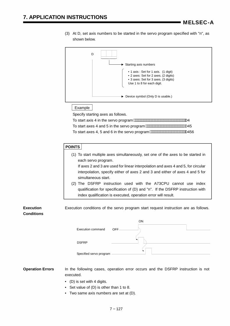
7. APPLICATION INSTRUCTIONS
7 − 127
MELSEC-A
(3) At D, set axis numbers to be started in the servo program specified with "n", as shown below.
Example Specify starting axes as follows. To start axis 4 in the servo program⋅⋅⋅⋅⋅⋅⋅⋅⋅⋅⋅⋅⋅⋅⋅⋅⋅⋅⋅⋅⋅⋅⋅⋅⋅⋅⋅⋅⋅⋅⋅⋅⋅⋅⋅⋅⋅⋅⋅⋅⋅⋅⋅⋅⋅⋅⋅⋅⋅⋅⋅⋅⋅ D4 To start axes 4 and 5 in the servo program⋅⋅⋅⋅⋅⋅⋅⋅⋅⋅⋅⋅⋅⋅⋅⋅⋅⋅⋅⋅⋅⋅⋅⋅⋅⋅⋅⋅⋅⋅⋅⋅⋅⋅⋅⋅⋅⋅⋅⋅ D45 To start axes 4, 5 and 6 in the servo program⋅⋅⋅⋅⋅⋅⋅⋅⋅⋅⋅⋅⋅⋅⋅⋅⋅⋅⋅⋅⋅⋅⋅⋅⋅⋅⋅⋅⋅⋅⋅⋅⋅⋅⋅⋅ D456
POINTS
(1) To start multiple axes simultaneously, set one of the axes to be started in each servo program.
If axes 2 and 3 are used for linear interpolation and axes 4 and 5, for circular interpolation, specify either of axes 2 and 3 and either of axes 4 and 5 for simultaneous start.
(2) The DSFRP instruction used with the A73CPU cannot use index qualification for specification of (D) and "n". If the DSFRP instruction with index qualification is executed, operation error will result.
Execution Execution conditions of the servo program start request instruction are as follows. Conditions
Operation Errors In the following cases, operation error occurs and the DSFRP instruction is not executed.
• (D) is set with 4 digits. • Set value of (D) is other than 1 to 8. • Two same axis numbers are set at (D).
Device symbol (Only D is usable.)
Starting axis numbers
• 1 axis : Set for 1 axis. (1 digit) • 2 axes: Set for 2 axes. (2 digits) • 3 axes: Set for 3 axes. (3 digits) Use 1 to 8 for each digit.
D
Execution command
DSFRP
Specified servo program
ON
OFF
7. APPLICATION INSTRUCTIONS
7 − 128
MELSEC-A
• Set value of "n" is outside of 0 to 4095 or 30000 to 30799. • Axes not specified at (D) are used in the servo program specified with "n". • Index qualification is used for specification of (D) and "n".
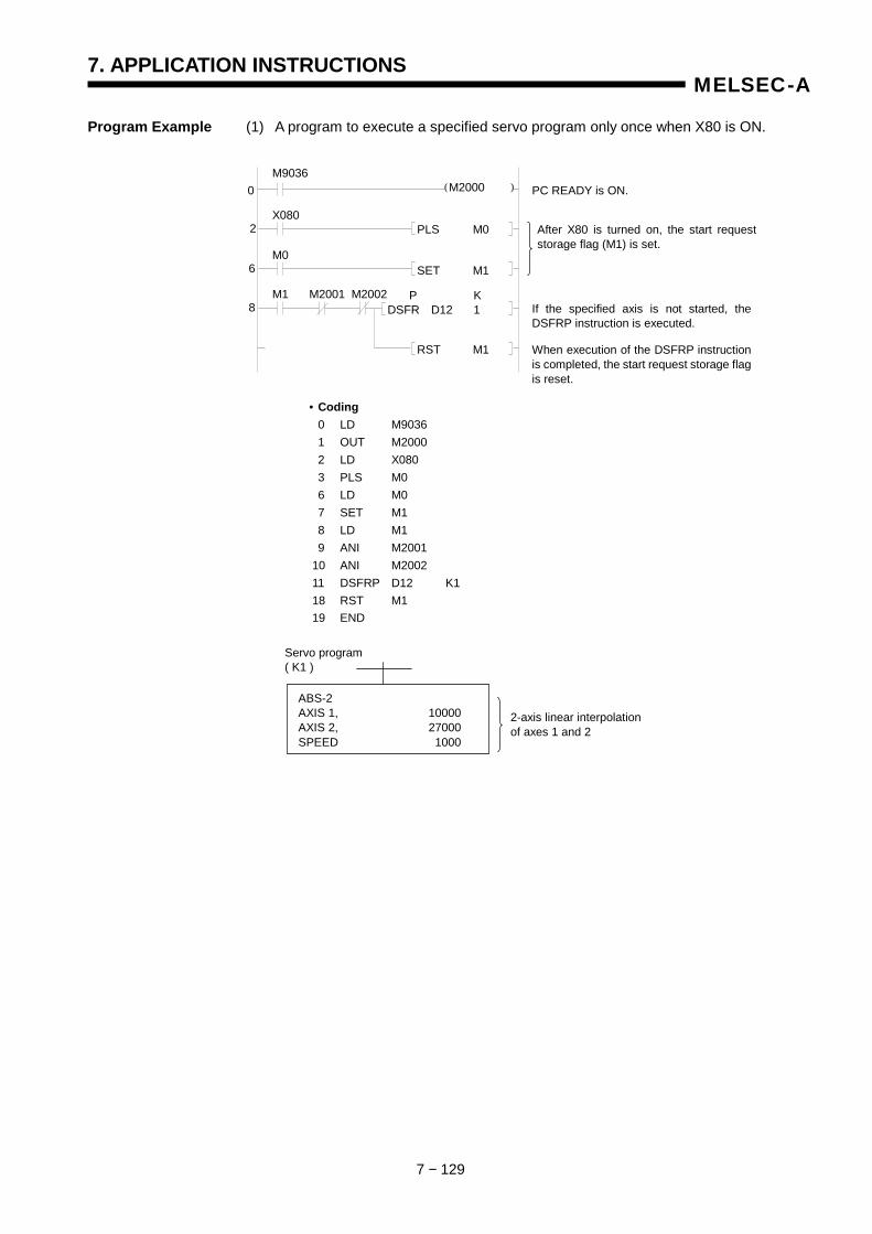
7. APPLICATION INSTRUCTIONS
7 − 129
MELSEC-A
Program Example (1) A program to execute a specified servo program only once when X80 is ON.
• Coding 0 LD M9036 1 OUT M2000 2 LD X080 3 PLS M0 6 LD M0 7 SET M1 8 LD M1 9 ANI M2001 10 ANI M2002 11 DSFRP D12 K1 18 RST M1 19 END
ABS-2 AXIS 1, 10000 AXIS 2, 27000 SPEED 1000
Servo program ( K1 )
2-axis linear interpolation of axes 1 and 2
When execution of the DSFRP instruction is completed, the start request storage flag is reset.
( ) PC READY is ON.
After X80 is turned on, the start requeststorage flag (M1) is set.
If the specified axis is not started, the DSFRP instruction is executed.
0
2
6
8
M9036
X080
M0
M1 M2001 M2002
M2000
PLS M0
SET M1
RST M1
P K DSFR D12 1
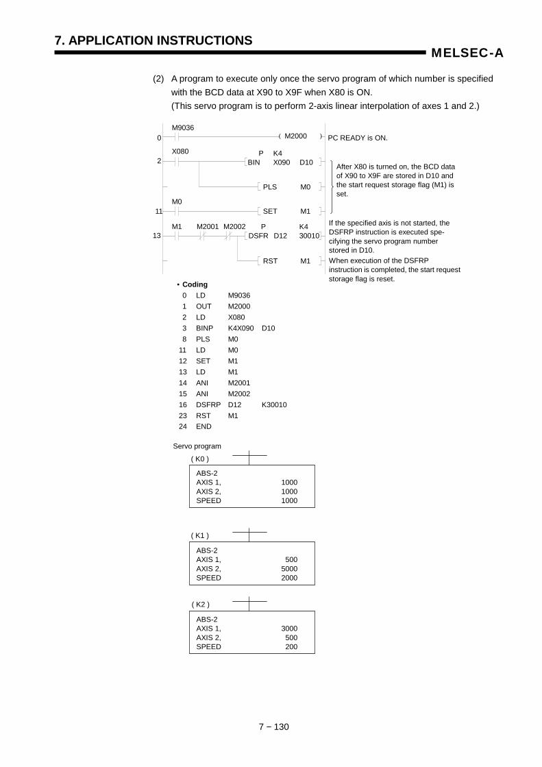
7. APPLICATION INSTRUCTIONS
7 − 130
MELSEC-A
(2) A program to execute only once the servo program of which number is specified with the BCD data at X90 to X9F when X80 is ON.
(This servo program is to perform 2-axis linear interpolation of axes 1 and 2.)
• Coding 0 LD M9036 1 OUT M2000 2 LD X080 3 BINP K4X090 D10 8 PLS M0 11 LD M0 12 SET M1 13 LD M1 14 ANI M2001 15 ANI M2002 16 DSFRP D12 K30010 23 RST M1 24 END
ABS-2 AXIS 1, 1000 AXIS 2, 1000 SPEED 1000
ABS-2 AXIS 1, 500 AXIS 2, 5000 SPEED 2000
ABS-2 AXIS 1, 3000 AXIS 2, 500 SPEED 200
( K0 )
Servo program
( K1 )
( K2 )
When execution of the DSFRP instruction is completed, the start request storage flag is reset.
After X80 is turned on, the BCD data of X90 to X9F are stored in D10 and the start request storage flag (M1) is set.
( ) PC READY is ON.
If the specified axis is not started, the DSFRP instruction is executed spe- cifying the servo program number stored in D10.
0
2
11
13
M9036
X080
M0
M1 M2001 M2002
M2000
P K4 BIN X090 D10
P K4 DSFR D12 30010
PLS M0
SET M1
RST M1
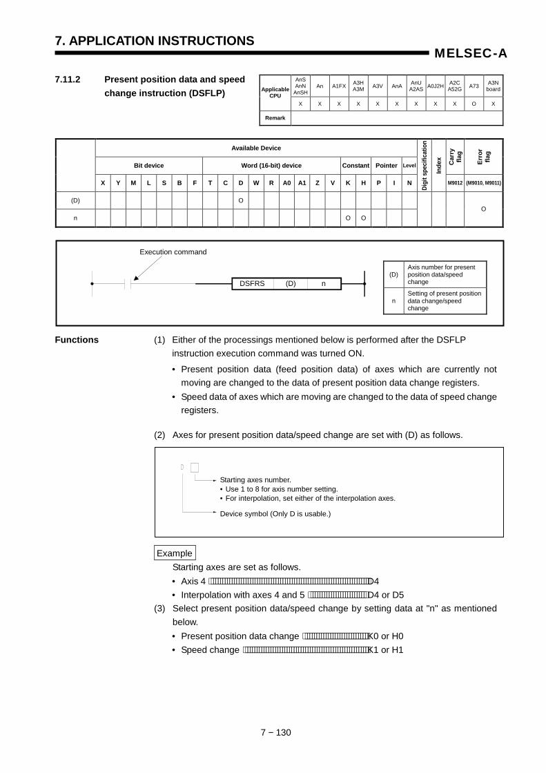
7. APPLICATION INSTRUCTIONS
7 − 130
MELSEC-A
7.11.2 Present position data and speed change instruction (DSFLP)
Available Device
Bit device Word (16-bit) device Constant Pointer Level Car
ry
flag
Erro
r fla
g
X Y M L S B F T C D W R A0 A1 Z V K H P I N
Digi
t spe
cific
atio
n
Inde
x
M9012 (M9010, M9011)
(D) O
n O O O
Functions (1) Either of the processings mentioned below is performed after the DSFLP instruction execution command was turned ON.
• Present position data (feed position data) of axes which are currently not moving are changed to the data of present position data change registers.
• Speed data of axes which are moving are changed to the data of speed change registers.
(2) Axes for present position data/speed change are set with (D) as follows.
Example Starting axes are set as follows.
• Axis 4 ⋅⋅⋅⋅⋅⋅⋅⋅⋅⋅⋅⋅⋅⋅⋅⋅⋅⋅⋅⋅⋅⋅⋅⋅⋅⋅⋅⋅⋅⋅⋅⋅⋅⋅⋅⋅⋅⋅⋅⋅⋅⋅⋅⋅⋅⋅⋅⋅⋅⋅⋅⋅⋅⋅⋅⋅⋅⋅⋅⋅⋅⋅⋅⋅⋅⋅⋅⋅⋅D4 • Interpolation with axes 4 and 5 ⋅⋅⋅⋅⋅⋅⋅⋅⋅⋅⋅⋅⋅⋅⋅⋅⋅⋅⋅⋅⋅⋅⋅⋅⋅ D4 or D5
(3) Select present position data/speed change by setting data at "n" as mentioned below. • Present position data change ⋅⋅⋅⋅⋅⋅⋅⋅⋅⋅⋅⋅⋅⋅⋅⋅⋅⋅⋅⋅⋅⋅⋅⋅⋅⋅⋅⋅ K0 or H0 • Speed change ⋅⋅⋅⋅⋅⋅⋅⋅⋅⋅⋅⋅⋅⋅⋅⋅⋅⋅⋅⋅⋅⋅⋅⋅⋅⋅⋅⋅⋅⋅⋅⋅⋅⋅⋅⋅⋅⋅⋅⋅⋅⋅⋅⋅⋅⋅⋅⋅⋅⋅⋅⋅⋅⋅ K1 or H1
AnSAnN
AnSHAn A1FX A3H
A3M A3V AnA AnU A2AS A0J2H A2C
A52G A73 A3NboardApplicable
CPU X X X X X X X X X O X
Remark
Execution command
DSFRS (D) n (D)
Axis number for present position data/speed change
n Setting of present position data change/speed change
Starting axes number. • Use 1 to 8 for axis number setting. • For interpolation, set either of the interpolation axes.
Device symbol (Only D is usable.)

7. APPLICATION INSTRUCTIONS
7 − 131
MELSEC-A
POINT
The DSFLP instruction used with the A73CPU cannot use index qualification for specification of (D) and "n". If the DSFLP instruction with index qualification is executed, operation error will result.
(4) Present position data change by the DSFLP instruction is performed as follows. 1) The start enable flag (M200n)* which corresponds to the axis specified with
(D) is set. 2) Present position data is changed to the data of present position data change
registers which correspond to the axes specified with (D). 3) When present position data change is completed, the start enable flag
(M200n) is reset.
Present position data change register numbers are provided as follows. Axis No. Axis 1 Axis 2 Axis 3 Axis 4 Axis 5 Axis 6 Axis 7 Axis 8
Upper date D961 D967 D973 D979 D985 D991 D997 D1003
Lower date D960 D966 D972 D978 D984 D990 D996 D1002
(5) Speed change by the DSFLP instruction is performed as follows.
1) The speed changing flag (M200n) which corresponds to the axis specified with (D) is set.
2) Positioning speed currently executed is changed to the data of speed change registers which correspond to the axes specified with (D).
3) The speed changing flag (M202n) is reset.
Speed change register numbers are provided as follows. Axis No. Axis 1 Axis 2 Axis 3 Axis 4 Axis 5 Axis 6 Axis 7 Axis 8
Upper date D963 D969 D975 D981 D987 D993 D999 D1005
Lower date D962 D968 D974 D980 D986 D992 D998 D1004
Execution Execution conditions of present position data/speed change are as follows. Conditions
Operation Errors In the following cases, an operation error occurs and the DSFLP instruction is not executed.
(1) Set value of (D) is other than 1 to 8.
Execution command
DSFLP instruction
ON
OFF
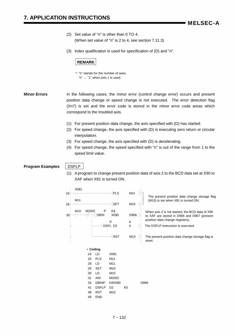
7. APPLICATION INSTRUCTIONS
7 − 132
MELSEC-A
(2) Set value of "n" is other than 0 TO 4. (When set value of "n" is 2 to 4, see section 7.11.3)
(3) Index qualification is used for specification of (D) and "n".
REMARK
*: "n" stands for the number of axes. "n" → "1" when axis 1 is used.
Minor Errors In the following cases, the minor error (control change error) occurs and present position data change or speed change is not executed. The error detection flag (Xn7) is set and the error code is stored in the minor error code areas which correspond to the troubled axis.
(1) For present position data change, the axis specified with (D) has started. (2) For speed change, the axis specified with (D) is executing zero return or circular
interpolation. (3) For speed change, the axis specified with (D) is decelerating. (4) For speed change, the speed specified with "n" is out of the range from 1 to the
speed limit value.
Program Examples DSFLP (1) A program to change present position data of axis 2 to the BCD data set at X90 to
XAF when X81 is turned ON.
• Coding 24 LD X081 25 PLS M11 28 LD M11 29 SET M10 30 LD M10 31 ANI M2002 32 DBINP K8X090 D966 41 DSFLP D2 K0 48 RST M10 49 END
The present position data change storage flag(M10) is set when X81 is turned ON.
When axis 2 is not started, the BCD data of X90to XAF are stored in D966 and D967 (presentposition data change registers).
The DSFLP instruction is executed.
The present position data change storage flag isreset.
24
28
30
X081 PLS M11
M11 SET M10
M10 M2002 P K8 DBIN X090 D966
P K DSFL D2 0
RST M10
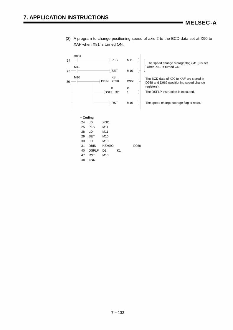
7. APPLICATION INSTRUCTIONS
7 − 133
MELSEC-A
(2) A program to change positioning speed of axis 2 to the BCD data set at X90 to
XAF when X81 is turned ON.
• Coding 24 LD X081 25 PLS M11 28 LD M11 29 SET M10 30 LD M10 31 DBIN K8X090 D968 40 DSFLP D2 K1 47 RST M10 48 END
The speed change storage flag (M10) is setwhen X81 is turned ON.
The BCD data of X90 to XAF are stored in D968 and D969 (positioning speed change registers). The DSFLP instruction is executed.
The speed change storage flag is reset.
24
28
30
X081 PLS M11
M11 SET M10
M10 K8 DBIN X090 D968
P K DSFL D2 1
RST M10

8. MICROCOMPUTER MODE
8 − 1
MELSEC-A
8. MICROCOMPUTER MODE
This section gives the microcomputer mode specifications, memory map and data memory configuration of the ACPU modules. Note that the AnA, A2AS and AnU cannot use the microcomputer mode.
8.1 Specifications of Microcomputer Mode
Module CPU (Clock)
Microcomputer Program Area Work Area Stack Area Instructions which
cannot be used *2
A1 0 to 10K bytes
A2 (S1) 0 to 26K bytes
A3
8086 (8 MHz) 0 to 58K bytes (Main)
0 to 58K bytes (Sub)
A1N 0 to 10K bytes
A2N (S1) 0 to 26K bytes
A3N 0 to 58K bytes (Main) 0 to 58K bytes (Sub)
A3V 0 to 58K bytes (Main) 0 to 58K bytes (Sub)
A73 0 to 58K bytes (Main) 0 to 58K bytes (Sub)
A52G
8086 (10 MHz)
0 to 14K bytes
A1SH, A1SJH
8086 (30 MHz) 0 to 14K bytes
A2SH (S1) 0 to 26K bytes
A1FX 8086
(40 MHz) 0 to 26K bytes
A0J2H 0 to 14K bytes
A2C 8086
(8 MHz) 0 to 14K bytes
INT, INTO, IRET, IN, OUT, HLT, WAIT, LOCK, ESC
A3H 0 to 58K bytes (Main) 0 to 58K bytes (Sub)
A3M
80286 (8 MHz) 0 to 58K bytes (Main)
0 to 58K bytes (Sub)
A100H to A1FFH (256 bytes)
User area: 128 bytes (No setting required by the user)
INT, INTO, IRET, IN, OUT, HLT, WAIT, LOCK, ESC, CLI, STI
Table 8.1 Specifications of Microcomputer Mode
*1: Specify the microcomputer program area in multiples of 2K bytes. The relation between the main (sub) program, sequence program, and microcomputer program capacities is as indicated below:
*2: Never use the instructions specified as those which cannot be used in preparing microcomputer programs. If they are used, the PC CPU will malfunction when a microcomputer program is run.
Main (sub) program memory
capacity
sequence program memory
capacity
microcomputer program memory
capacity = +
*1
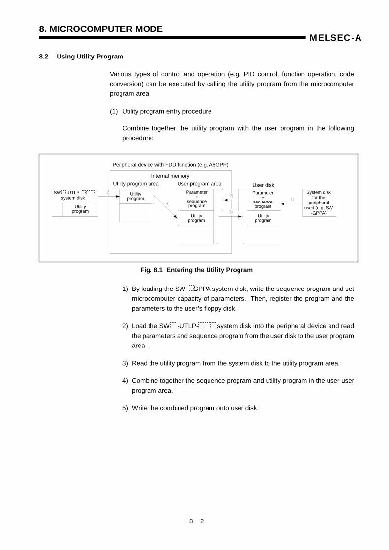
8. MICROCOMPUTER MODE
8 − 2
MELSEC-A
8.2 Using Utility Program
Various types of control and operation (e.g. PID control, function operation, code conversion) can be executed by calling the utility program from the microcomputer program area.
(1) Utility program entry procedure
Combine together the utility program with the user program in the following procedure:
Fig. 8.1 Entering the Utility Program
1) By loading the SW -GPPA system disk, write the sequence program and set microcomputer capacity of parameters. Then, register the program and the parameters to the user’s floppy disk.
2) Load the SW -UTLP- system disk into the peripheral device and read
the parameters and sequence program from the user disk to the user program area.
3) Read the utility program from the system disk to the utility program area.
4) Combine together the sequence program and utility program in the user user program area.
5) Write the combined program onto user disk.
Utility program
SW -UTLP- system disk
Utility program
Utilityprogram
Utilityprogram
Parameter+
sequenceprogram
Parameter+
sequenceprogram
System disk for the
peripheral used (e.g. SW
-GPPA)
Utility program area User program areaInternal memory
Peripheral device with FDD function (e.g. A6GPP)
User disk
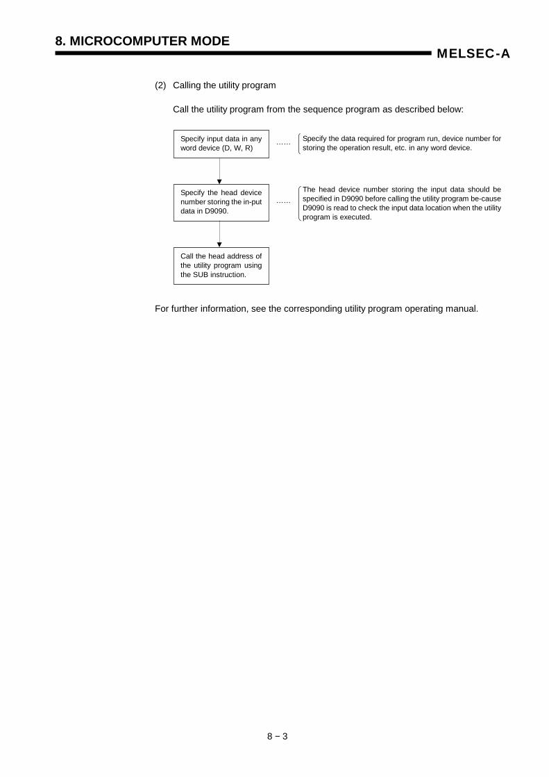
8. MICROCOMPUTER MODE
8 − 3
MELSEC-A
(2) Calling the utility program
Call the utility program from the sequence program as described below:
For further information, see the corresponding utility program operating manual.
Call the head address ofthe utility program usingthe SUB instruction.
Specify input data in anyword device (D, W, R)
Specify the data required for program run, device number for storing the operation result, etc. in any word device.
……
Specify the head devicenumber storing the in-putdata in D9090.
The head device number storing the input data should be specified in D9090 before calling the utility program be-cause D9090 is read to check the input data location when the utility program is executed.
……
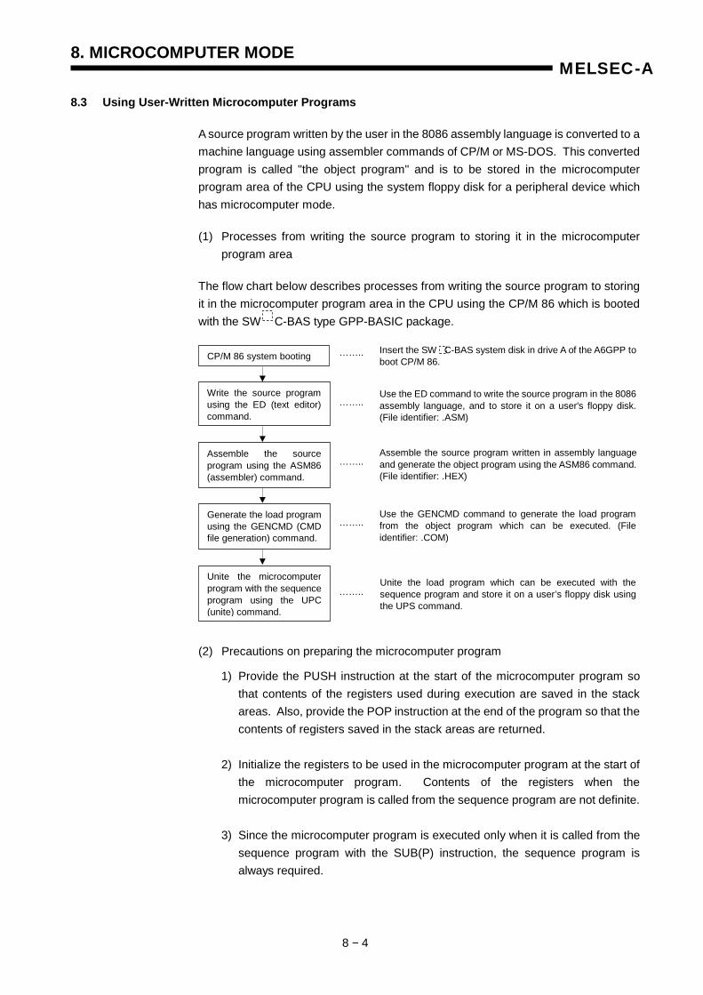
8. MICROCOMPUTER MODE
8 − 4
MELSEC-A
8.3 Using User-Written Microcomputer Programs
A source program written by the user in the 8086 assembly language is converted to a machine language using assembler commands of CP/M or MS-DOS. This converted program is called "the object program" and is to be stored in the microcomputer program area of the CPU using the system floppy disk for a peripheral device which has microcomputer mode.
(1) Processes from writing the source program to storing it in the microcomputer program area
The flow chart below describes processes from writing the source program to storing it in the microcomputer program area in the CPU using the CP/M 86 which is booted with the SW C-BAS type GPP-BASIC package.
(2) Precautions on preparing the microcomputer program
1) Provide the PUSH instruction at the start of the microcomputer program so that contents of the registers used during execution are saved in the stack areas. Also, provide the POP instruction at the end of the program so that the contents of registers saved in the stack areas are returned.
2) Initialize the registers to be used in the microcomputer program at the start of
the microcomputer program. Contents of the registers when the microcomputer program is called from the sequence program are not definite.
3) Since the microcomputer program is executed only when it is called from the
sequence program with the SUB(P) instruction, the sequence program is always required.
CP/M 86 system booting Insert the SW C-BAS system disk in drive A of the A6GPP toboot CP/M 86.
……..
Write the source program using the ED (text editor) command.
Use the ED command to write the source program in the 8086assembly language, and to store it on a user's floppy disk.(File identifier: .ASM)
……..
Assemble the source program using the ASM86 (assembler) command.
Assemble the source program written in assembly language and generate the object program using the ASM86 command. (File identifier: .HEX)
……..
Generate the load programusing the GENCMD (CMDfile generation) command.
Use the GENCMD command to generate the load program from the object program which can be executed. (File identifier: .COM)
……..
Unite the microcomputerprogram with the sequenceprogram using the UPC(unite) command.
Unite the load program which can be executed with thesequence program and store it on a user’s floppy disk usingthe UPS command.
……..
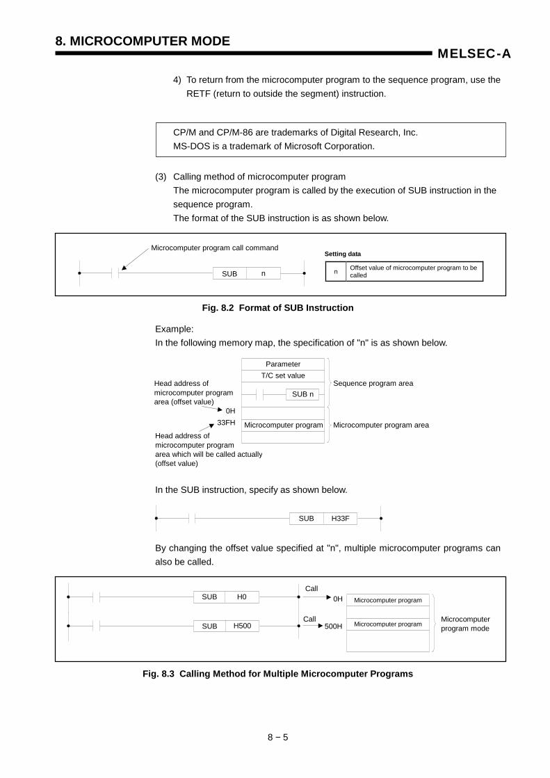
8. MICROCOMPUTER MODE
8 − 5
MELSEC-A
4) To return from the microcomputer program to the sequence program, use the RETF (return to outside the segment) instruction.
CP/M and CP/M-86 are trademarks of Digital Research, Inc. MS-DOS is a trademark of Microsoft Corporation.
(3) Calling method of microcomputer program The microcomputer program is called by the execution of SUB instruction in the sequence program. The format of the SUB instruction is as shown below.
Fig. 8.2 Format of SUB Instruction
Example: In the following memory map, the specification of "n" is as shown below.
In the SUB instruction, specify as shown below.
By changing the offset value specified at "n", multiple microcomputer programs can also be called.
Fig. 8.3 Calling Method for Multiple Microcomputer Programs
n Offset value of microcomputer program to be called
Setting data
SUB n
Microcomputer program call command
Head address of microcomputer program area which will be called actually(offset value)
SUB H33F
0H
500H
Microcomputer program
Microcomputer program Microcomputer program mode
Call
Call
SUB H0
SUB H500
Head address of microcomputer program area (offset value)
Sequence program area
Microcomputer program area
0H33FH
ParameterT/C set value
SUB n
Microcomputer program
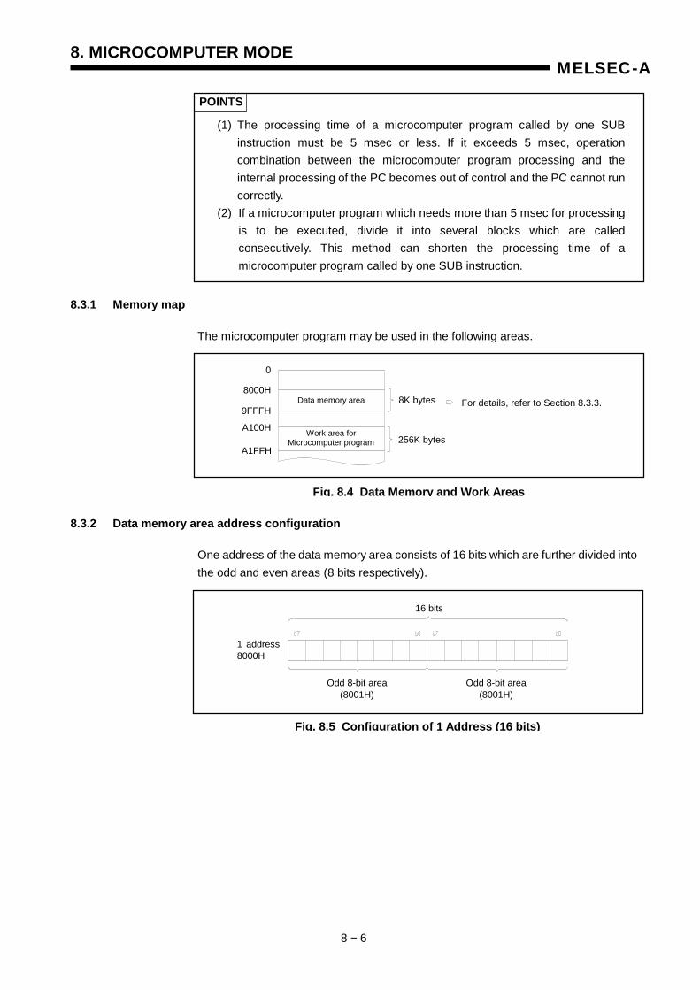
8. MICROCOMPUTER MODE
8 − 6
MELSEC-A
POINTS
(1) The processing time of a microcomputer program called by one SUB instruction must be 5 msec or less. If it exceeds 5 msec, operation combination between the microcomputer program processing and the internal processing of the PC becomes out of control and the PC cannot run correctly.
(2) If a microcomputer program which needs more than 5 msec for processing is to be executed, divide it into several blocks which are called consecutively. This method can shorten the processing time of a microcomputer program called by one SUB instruction.
8.3.1 Memory map
The microcomputer program may be used in the following areas.
8.3.2 Data memory area address configuration
One address of the data memory area consists of 16 bits which are further divided into the odd and even areas (8 bits respectively).
Data memory area
Work area for Microcomputer program
A1FFH
A100H
9FFFH
8000H
0
8K bytes
256K bytes
For details, refer to Section 8.3.3.
Fig. 8.4 Data Memory and Work Areas
16 bits
1 address8000H
Odd 8-bit area (8001H)
Odd 8-bit area (8001H)
Fig. 8.5 Configuration of 1 Address (16 bits)
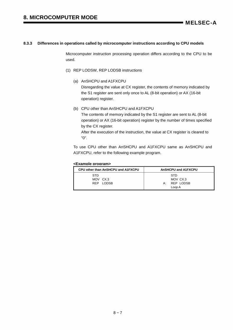
8. MICROCOMPUTER MODE
8 − 7
MELSEC-A
8.3.3 Differences in operations called by microcomputer instructions according to CPU models
Microcomputer instruction processing operation differs according to the CPU to be used.
(1) REP LODSW, REP LODSB instructions
(a) AnSHCPU and A1FXCPU Disregarding the value at CX register, the contents of memory indicated by the S1 register are sent only once to AL (8-bit operation) or AX (16-bit operation) register.
(b) CPU other than AnSHCPU and A1FXCPU The contents of memory indicated by the S1 register are sent to AL (8-bit operation) or AX (16-bit operation) register by the number of times specified by the CX register. After the execution of the instruction, the value at CX register is cleared to "0".
To use CPU other than AnSHCPU and A1FXCPU same as AnSHCPU and A1FXCPU, refer to the following example program.
CPU other than AnSHCPU and A1FXCPU AnSHCPU and A1FXCPU
STD MOV CX.3 REP LODSB
STD MOV CX.3 A: REP LODSB Loop A
<Example program>
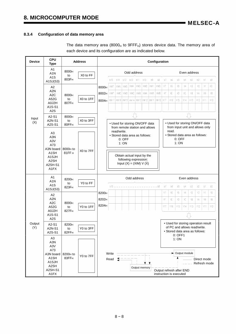
8. MICROCOMPUTER MODE
8 − 8
MELSEC-A
8.3.4 Configuration of data memory area
The data memory area (8000H to 9FFFH) stores device data. The memory area of each device and its configuration are as indicated below.
Device CPU Type Address Configuration
A1 A1N A1S
A1SJ(S3)
8000Hto
803FH X0 to FF
A2 A2N A2C
A52G A0J2H A1S-S1
A2S
8000Hto
807FH X0 to 1FF
A2-S1 A2N-S1 A2S-S1
8000Hto
80FFH X0 to 3FF
Input (X)
A3 A3N A3V A73
A3N board A1SH A1SJH A2SH
A2SH-S1 A1FX
8000H to 81FF H X0 to 7FF
A1 A1N A1S
A1SJ(S3)
8200Hto
823FH Y0 to FF
A2 A2N A2C
A52G A0J2H A1S-S1
A2S
8000Hto
827FH Y0 to 1FF
A2-S1 A2N-S1 A2S-S1
8200Hto
82FFH Y0 to 3FF
Output (Y)
A3 A3N A3V A73
A3N board A1SH A1SJH A2SH
A2SH-S1 A1FX
8200H to 83FFH Y0 to 7FF
8200H
8202H
8204H
Odd address Even address
• Used for storing operation result of PC and allows read/write.
• Stored data area as follows: 0: OFF1
1: ON
Write
Read Direct modeRefresh mode
Output module
Output refresh after END instruction is executed
Output memory
8000H
8002H
8004H
Obtain actual input by the following expression:
Input (X) = (XIM) V (X)
Odd address Even address
• Used for storing ON/OFF data from input unit and allows only read.
• Stored data area as follows: 0: OFF
1: ON
• Used for storing ON/OFF data from remote station and allows read/write.
• Stored data area as follows: 0: OFF
1: ON
8. MICROCOMPUTER MODE
8 − 9
MELSEC-A
REMARK
Communication of input/output information with an input/output module is executed only in the address range indicated below. A1FX: X/Y20 to FF A1SH, A1SJH: X/Y0 to FF A2SH: X/Y0 to 1FF A2SH-S1: X/Y0 to 3FF
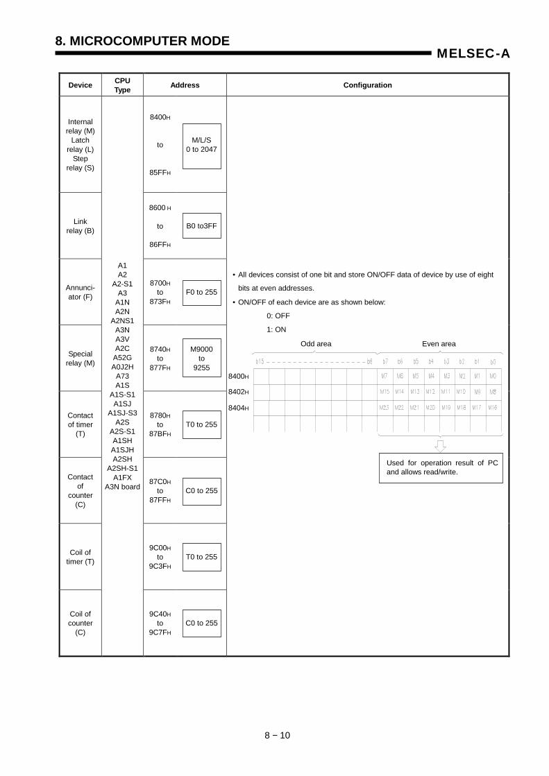
8. MICROCOMPUTER MODE
8 − 10
MELSEC-A
Device CPU Type Address Configuration
Internal relay (M)
Latch relay (L)
Step relay (S)
8400H
to
85FFH
M/L/S 0 to 2047
Link relay (B)
8600 H
to
86FFH
B0 to3FF
Annunci- ator (F)
8700Hto
873FH F0 to 255
Special relay (M)
8740Hto
877FH
M9000 to
9255
Contact of timer
(T)
8780Hto
87BFH T0 to 255
Contact of
counter (C)
87C0Hto
87FFH C0 to 255
Coil of timer (T)
9C00Hto
9C3FH T0 to 255
Coil of counter
(C)
A1 A2
A2-S1 A3
A1N A2N
A2NS1 A3N A3V A2C
A52G A0J2H
A73 A1S
A1S-S1 A1SJ
A1SJ-S3 A2S
A2S-S1 A1SH A1SJH A2SH
A2SH-S1 A1FX
A3N board
9C40Hto
9C7FH C0 to 255
8400H
8402H
8404H
• All devices consist of one bit and store ON/OFF data of device by use of eight
bits at even addresses.
• ON/OFF of each device are as shown below:
0: OFF
1: ON
Odd area Even area
Used for operation result of PCand allows read/write.
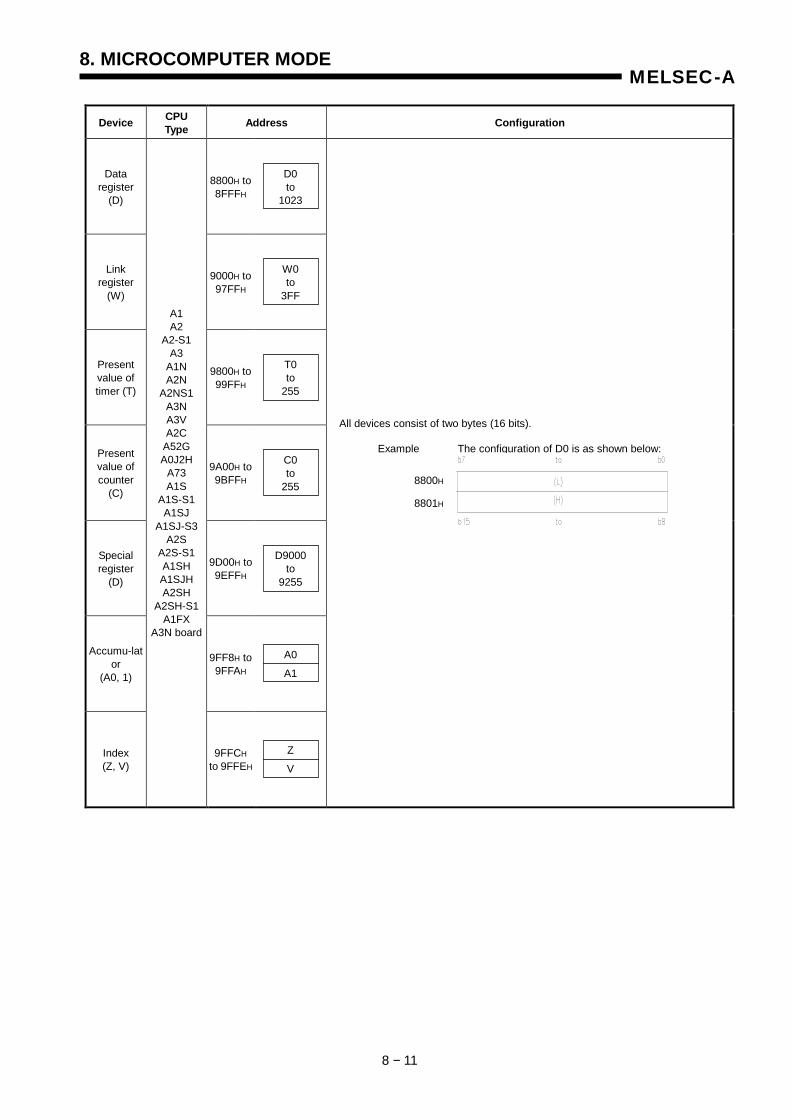
8. MICROCOMPUTER MODE
8 − 11
MELSEC-A
Device CPU Type Address Configuration
Data register
(D)
8800H to 8FFFH
D0 to
1023
Link register
(W)
9000H to 97FFH
W0 to
3FF
Present value of timer (T)
9800H to 99FFH
T0 to
255
Present value of counter
(C)
9A00H to 9BFFH
C0 to
255
Special register
(D)
9D00H to 9EFFH
D9000 to
9255
Accumu-lator
(A0, 1)
9FF8H to 9FFAH
A0
A1
Index (Z, V)
A1 A2
A2-S1 A3
A1N A2N
A2NS1 A3N A3V A2C
A52G A0J2H
A73 A1S
A1S-S1 A1SJ
A1SJ-S3 A2S
A2S-S1 A1SH A1SJH A2SH
A2SH-S1 A1FX
A3N board
9FFCH to 9FFEH
Z
V
All devices consist of two bytes (16 bits).
Example The configuration of D0 is as shown below:
8800H
8801H
8. MICROCOMPUTER MODE
8 − 12
MELSEC-A
Device CPU Type Address Configuration
Input (X)
8000H
to
80FFH
X0 to 7FF
Output (Y)
8200H
to
82FFH
Y0 to 7FF
Internal relay (M)
Latch relay (L)
Step relay (S)
8400H to
84FFH
M/L/S 0 to 2047
Link relay (B)
8600H to
867FH B0 to 3FF
Annuci-ator (F)
A3H A3M
8700H to
871FH F0 to 255
• Stores PC operation results and allows read/write.
• Stores device ON/OFF data in one bit locations. • 0 indicates OFF and 1 ON. Example: M0 to 47 are as follows:
8200H
8202H
8204H
Odd area Even area
8000H
8002H
8004H
• Stores ON/OFF data from an input unit, read only. • 0 indicates OFF and 1 ON.
Odd address Even address
8200H
8202H
8204H
Odd address Even address
• Stores PC operation results and allows read/write. • 0 indicates OFF and 1 ON.
The output memory is accessed as below?
Write
ReadDirect modeRefresh mode
Output module
Output memory
Output refresh after END instruction is executed
9. ERROR CODE LIST
9 − 1
MELSEC-A
9. ERROR CODE LIST
If an error occurred when the PC is in RUN mode, error indication is given by self-checking function and corresponding error code and error step are stored in special registers. This section gives description of cause and corrective action for each case of error.
9.1 Reading Error Codes
If an error occurred, corresponding error code can be read from the peripheral. For details, refer to the operation manual of the peripheral.
9.2 Error Code List for the CPUs of Other Than AnACPU, A2ASCPU and AnUCPU
Table 9.1 shows the error messages, description and cause of error and corrective actions. Error codes and error steps are stored in the following special registers. Error code: D9008 Error step: D9010 and D9011
Table 9.1 Error Code List for the CPUs of Other Than AnA, A2AS and AnU (Continue)
Error Message Error Code (D9008)
CPU States Error and Cause Corrective Action
"INSTRCT. CODE ERR" (Checked at
the execution of instruction)
10 Stop Instruction code, which cannot be decoded by CPU, is included in the program. (1) ROM including instruction code, which cannot be decoded, has been loaded. (2) Since the memory contents have changed for some reason, instruction code, which cannot be decoded, has been included.
(1) Read the error step by use of a peripheral equipment and correct the program at that step. (2) In the case of ROM, rewrite the contents of change the ROM with a ROM which stores correct contents.
"PARAMETER ERROR"
(Checked at power-on,
STOP → RUN, and
PAUSE → RUN)
11 Stop (1) Capacity larger than the memory capacity of CPU has been set and then write to CPU has been performed. (2) The contents of parameters of CPU memory have changed due to noise or the improper loading of memory. (3) RAM is not loaded to the A1 or A1N.
(1) Check the memory capacity of CPU with the memory capacity set by peripheral equipment and re-set incorrect area. (2) Check the loading of CPU memory and load it correctly. Read the parameter contents of CPU memory, check and correct the contents, and write them to CPU again. (3) Install the RAM and write parameter contents from a peripheral device.
"MISSING END INS."
(Checked at STOP → RUN)
12 Stop (1) There is no END (FEND) instruction in the program. (2) When subprogram has been set by the parameter, there is no END instruction in the subprogram.
Write END instruction at the end of program.
9. ERROR CODE LIST
9 − 2
MELSEC-A
Table 9.1 Error Code List for the CPUs of Other Than AnA, A2AS and AnU(Continue)
Error Message Error Code (D9008)
CPU States Error and Cause Corrective Action
"CAN’T EXECUTE(P)" (Checked at
the execution of instruction)
13 Stop (1) There is no jump destination or multiple destinations specified by the CJ , SCJ , CALL , CALLP , or JMP instruction. (2) There is a CHG instruction and no setting of subprogram. (3) Although there is no CALL instruction, the RET instruction exists in the program and has been executed. (4) The CJ , SCJ , CALL , CALLP , or JMP instruction has been executed with its jump destination located below the END instruction. (5) The number of the FOR instructions is different from that of the NEXT instructions. (6) A JMP instruction is given within a FOR to NEXT loop causing the processing to exit the loop. (7) Processing exited subroutine by the JMP instruction before execution of the RET instruction.(8) Processing jumped into a step in a FOR to NEXT loop or into a subroutine by the JMP instruction. (9) The STOP instruction is given in an interrupt program, a subroutine program or in a FOR to NEXT loop.
Read the error step by use of peripheral equipment and correct the program at that step.
"CHK FORMAT ERR"
(Checked at STOP/PAUSE→
RUN)
14 Stop (1) Instructions (including NOP ) except LD X , LDI X , AND X and ANI X are included in the CHK instruction circuit block. (2) Multiple CHK instructions are given. (3) The number of contact points in the CHK instruction circuit block exceeds 150. (4) There is no circuit block before the CHK instruction circuit block. (5) The device number of D1 of the CHK D1 D2 instruction is different from that of the contact point before the CPJ instruction.(6) Pointer P254 is not given to the head of the CHK instruction circuit block.
Check the program in the CHK instruction circuit block according to items (1) to (6) in the left column. Correct problem using the peripheral and perform operation again.
CJ P
P254 CHK D1 D2
9. ERROR CODE LIST
9 − 3
MELSEC-A
Table 9.1 Error Code List for the CPUs of Other Than AnA, A2AS and AnU (Continue)
Error Message Error Code (D9008)
CPU States Error and Cause Corrective Action
"CAN’T EXECUTE (I)"
(Checked at the occurrence of interruption)
15 Stop (1) Although the interrupt module is used, there is no number of interrupt pointer I, which corresponds to that module, in the program or there are multiple numbers. (2) No IRET instruction has been entered in the interrupt program. (3) There is IRET instruction in other than the interrupt program.
(1) Check for the presence of interrupt program which corresponds to the interrupt unit and reduce the same numbers of I. (2) Check if there is IRET instruction in the interrupt program and enter the IRET instruction. (3) Check if there is IRET instruction in other than the interrupt program and delete the IRET instruction.
"CASSETTE ERROR"
(Checked at power-on)
16 Stop The memory cassette is not loaded. Turn off the power, insert the memory cassette and turn on the power again.
ROM ERR 17 Stop (1) Parameters and/or sequence programs are not correctly written to the installed memory cassette. A1S(S1), A1SJ(S3), A2S(S1), A1SH, A1SJH, A2SH(S1), A1FX
(1) Write parameters and/or sequence programs correctly to the memory cassette. (2) Remove a memory cassette which does not have any parameter and/or sequence program.
"RAM ERROR" (Checked at power-on)
20 Stop The CPU has checked if write and read operations can be performed properly to the data memory area of CPU, and as a result, either or both has not been performed.
"OPE. CIRCUIT ERR"
(Checked at power-on)
21 Stop The operation circuit, which performs the sequence processing in the CPU, does not operate properly.
Since this CPU hardware error, consult Mitsubishi representative.
"WDT ERROR" (Checked at the
execution of END processing)
22 Stop Scan time exceeds watch dog error monitor time. (1) Scan timer of user program has been exceeded. (2) Scan time has lengthened due to instantaneous power failure which occurred during scan.
(1) Calculate and check the scan time of user program and reduce the scan time. (2) Monitor the content of special register D9005 by use of peripheral equipment. When the content is other than 0, line voltage is insufficient. Therefore, check the power and reduce the fluctuation of voltage.
"SUB-CPU ERROR" (Checked
continuously)
23 (During run)
26 (At power-on)
Stop Sub-CPU is locked-up or defective. Since this CPU hardware error, consult Mitsubishi representative.
"END NOT EXECUTE"
(Checked at the execution of
END instruction)
24 Stop The END instruction has changed to another instruction code for some reason.
Perform reset and run. If the same error is displayed again, it is the CPU hardware error. Therefore, consult nearby service center, representative, or branch.
"WDT ERROR" (Checked
continuously)
25 Stop (1) The CPU is executing an endless loop. (2) Main-CPU is malfunctioning.
(1) Since the program is in an endless loop due to the JMP and CJ instructions, check the program. (2) Since this CPU hardware error, consult Mitsubishi representative.
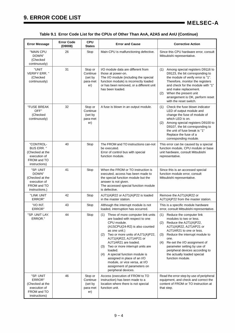
9. ERROR CODE LIST
9 − 4
MELSEC-A
Table 9.1 Error Code List for the CPUs of Other Than AnA, A2AS and AnU (Continue)
Error Message Error Code (D9008)
CPU States Error and Cause Corrective Action
"MAIN CPU DOWN"
(Checked continuously)
26 Stop Main-CPU is malfunctioning defective. Since this CPU hardware error, consult Mitsubishi representative.
"UNIT VERIFY ERR. "
(Checked continuously)
31 Stop or Continue (set by
para-meter)
I/O module data are different from those at power-on. The I/O module (including the special function module) is incorrectly loaded or has been removed, or a different unit has been loaded.
(1) Among special registers D9116 to D9123, the bit corresponding to the module of verify error is "1". Therefore, monitor the registers and check for the module with "1" and make replacement. (2) When the present unit arrangement is OK, perform reset with the reset switch.
"FUSE BREAK OFF"
(Checked continuously)
32 Stop or Continue (set by
para-meter)
A fuse is blown in an output module. (1) Check the fuse blown indicator LED of output module and change the fuse of module of which LED is on. (2) Among special registers D9100 to D9107, the bit corresponding to the unit of fuse break is "1" Replace the fuse of a corresponding module.
"CONTROL- BUS ERR. "
(Checked at the execution of
FROM and TO instructions)
40 Stop The FROM and TO instructions can-not be executed. Error of control bus with special function module.
This error can be caused by a special function module, CPU module or base unit hardware, consult Mitsubishi representative.
"SP. UNIT DOWN"
(Checked at the execution of
FROM and TO instructions.)
41 Stop When the FROM or TO instruction is executed, access has been made to the special function module but the answer is not given. The accessed special function module is defective.
Since this is an accessed special function module error, consult Mitsubishi representative.
"LINK UNIT ERROR"
42 Stop AJ71(A)R22 or AJ71(A)P22 is loaded in the master station.
Remove the AJ71(A)R22 or AJ71(A)P22 from the master station.
"I/O INT. ERROR"
43 Stop Although the interrupt module is not loaded, interruption has occurred.
This is a specific module hardware error, consult Mitsubishi representative.
"SP. UNIT LAY. ERROR."
44 Stop (1) Three of more computer link units are loaded with respect to one CPU module. (A1SCPU(24-R2) is also counted as one unit.) (2) Two or more units of AJ71(A)P22, AJ71(A)R22, AJ71AP21 or AJ71AR21 are loaded. (3) Two or more interrupt units are loaded. (4) A special function module is assigned in place of an I/O module, or vice versa, at I/O assignment of parameters on peripheral devices.
(1) Reduce the computer link modules to two or less. (2) Reduce the AJ71(A)P22, AJ71(A)R22, AJ71AP21 or AJ71AR21 to one or less. (3) Reduce the interrupt module to one. (4) Re-set the I/O assignment of parameter setting by use of peripheral devices according to the actually loaded special function module.
"SP. UNIT ERROR"
(Checked at the execution of
FROM and TO instructions)
46 Stop or Continue (set by
para-meter)
Access (execution of FROM to TO instruction) has been made to a location where there is not special function unit.
Read the error step by use of peripheral equipment, and check and correct the content of FROM or TO instruction at that step.
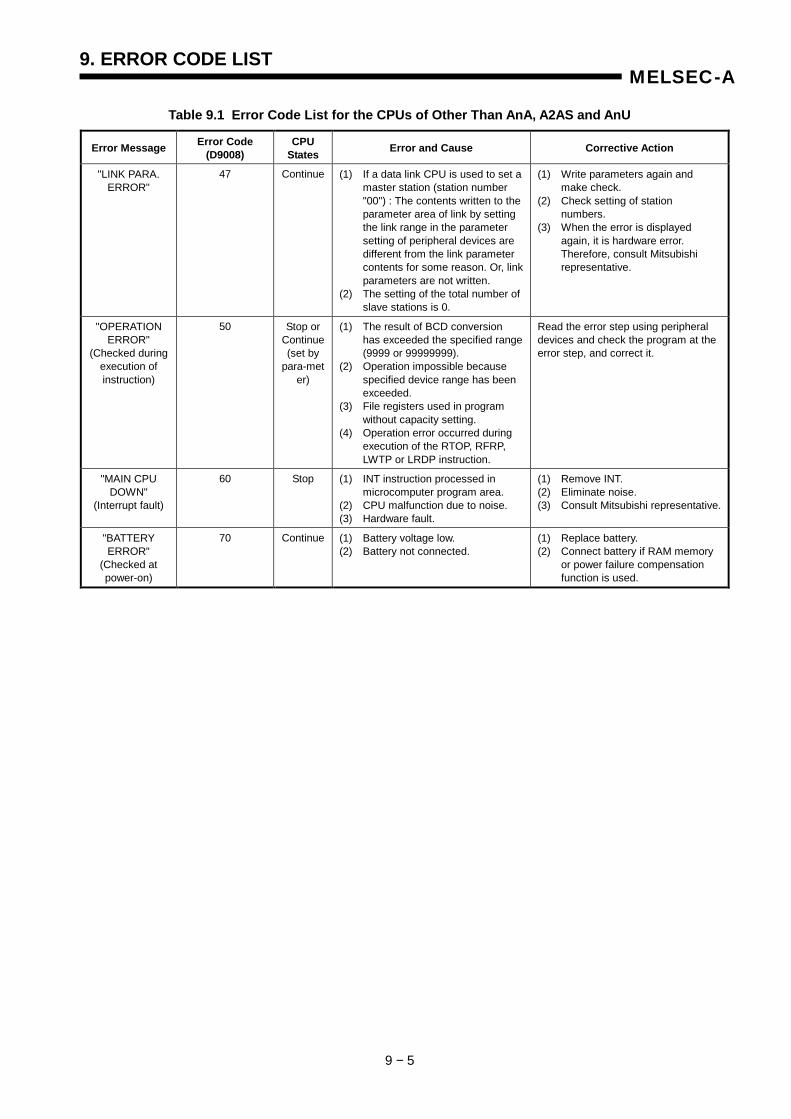
9. ERROR CODE LIST
9 − 5
MELSEC-A
Table 9.1 Error Code List for the CPUs of Other Than AnA, A2AS and AnU
Error Message Error Code (D9008)
CPU States Error and Cause Corrective Action
"LINK PARA. ERROR"
47 Continue (1) If a data link CPU is used to set a master station (station number "00") : The contents written to the parameter area of link by setting the link range in the parameter setting of peripheral devices are different from the link parameter contents for some reason. Or, link parameters are not written. (2) The setting of the total number of slave stations is 0.
(1) Write parameters again and make check. (2) Check setting of station numbers. (3) When the error is displayed again, it is hardware error. Therefore, consult Mitsubishi representative.
"OPERATION ERROR"
(Checked during execution of instruction)
50 Stop or Continue (set by
para-meter)
(1) The result of BCD conversion has exceeded the specified range (9999 or 99999999). (2) Operation impossible because specified device range has been exceeded. (3) File registers used in program without capacity setting. (4) Operation error occurred during execution of the RTOP, RFRP, LWTP or LRDP instruction.
Read the error step using peripheral devices and check the program at the error step, and correct it.
"MAIN CPU DOWN"
(Interrupt fault)
60 Stop (1) INT instruction processed in microcomputer program area. (2) CPU malfunction due to noise. (3) Hardware fault.
(1) Remove INT. (2) Eliminate noise. (3) Consult Mitsubishi representative.
"BATTERY ERROR"
(Checked at power-on)
70 Continue (1) Battery voltage low. (2) Battery not connected.
(1) Replace battery. (2) Connect battery if RAM memory or power failure compensation function is used.
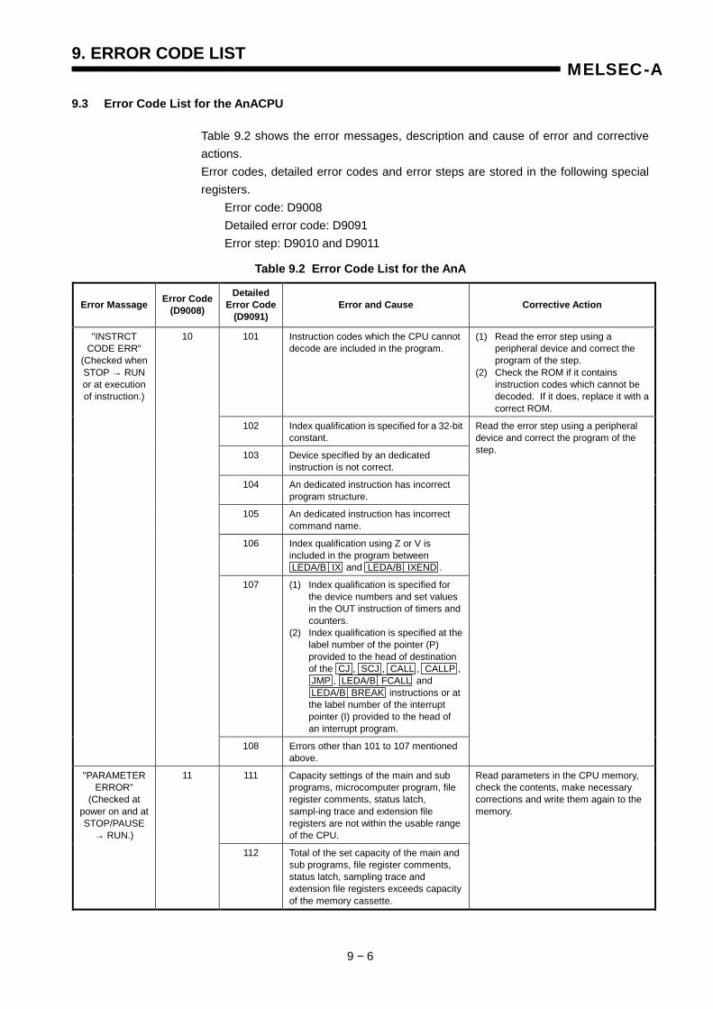
9. ERROR CODE LIST
9 − 6
MELSEC-A
9.3 Error Code List for the AnACPU
Table 9.2 shows the error messages, description and cause of error and corrective actions. Error codes, detailed error codes and error steps are stored in the following special registers. Error code: D9008 Detailed error code: D9091 Error step: D9010 and D9011
Table 9.2 Error Code List for the AnA
Error Massage Error Code(D9008)
Detailed Error Code
(D9091) Error and Cause Corrective Action
101 Instruction codes which the CPU cannot decode are included in the program.
(1) Read the error step using a peripheral device and correct the program of the step. (2) Check the ROM if it contains instruction codes which cannot be decoded. If it does, replace it with a correct ROM.
102 Index qualification is specified for a 32-bit constant.
103 Device specified by an dedicated instruction is not correct.
104 An dedicated instruction has incorrect program structure.
105 An dedicated instruction has incorrect command name.
106 Index qualification using Z or V is included in the program between LEDA/B IX and LEDA/B IXEND .
107 (1) Index qualification is specified for the device numbers and set values in the OUT instruction of timers and counters. (2) Index qualification is specified at the label number of the pointer (P) provided to the head of destination of the CJ , SCJ , CALL , CALLP , JMP , LEDA/B FCALL and LEDA/B BREAK instructions or at the label number of the interrupt pointer (I) provided to the head of an interrupt program.
"INSTRCT CODE ERR"
(Checked when STOP → RUN or at execution of instruction.)
10
108 Errors other than 101 to 107 mentioned above.
Read the error step using a peripheral device and correct the program of the step.
111 Capacity settings of the main and sub programs, microcomputer program, file register comments, status latch, sampl-ing trace and extension file registers are not within the usable range of the CPU.
"PARAMETER ERROR"
(Checked at power on and at STOP/PAUSE
→ RUN.)
11
112 Total of the set capacity of the main and sub programs, file register comments, status latch, sampling trace and extension file registers exceeds capacity of the memory cassette.
Read parameters in the CPU memory, check the contents, make necessary corrections and write them again to the memory.

9. ERROR CODE LIST
9 − 7
MELSEC-A
Table 9.2 Error Code List for the AnA (Continue)
Error Massage Error Code(D9008)
Detailed Error Code
(D9091) Error and Cause Corrective Action
113 Latch range set by parameters or setting of M, L or S is incorrect.
114 Sum check error
115 Either of settings of the remote RUN/ PAUSE contact point by parameters, operation mode at occurrence of error, annunciator indication mode, or STOP → RUN indication mode is incorrect.
116 The MNET-MINI automatic refresh setting by parameters is incorrect.
117 Timer setting by parameters is incorrect.
"PARAMETER ERROR"
(Checked at power on and at STOP/PAUSE
→ RUN.)
11
118 Counter setting by parameters is incorrect.
Read parameters in the CPU memory, check the contents, make necessary corrections and write them again to the memory
121 The END (FEND) instruction is not given in the main program.
Write the END instruction at the end of the main program.
"MISSING END INS"
(Checked at STOP → RUN.)
12
122 The END (FEND) instruction is not given in the sub program if the sub program is set by parameters.
Write the END instruction at the end of the sub program.
131 The same device number is used at two or more steps for the pointers (P) and interrupt pointers (I) used as labels to be specified at the head of jump destination.
Eliminate the same pointer numbers provided at the head of jump destination.
132 Label of the pointer (P) specified in the CJ , SCJ , CALL , CALLP , JMP , LEDA/B FCALL or LEDA/B BREAK instruction is not provided before the END instruction.
Read the error step using a peripheral device, check contents and insert a jump destination pointer (P).
133 (1) The RET instruction was included in the program and executed though the CALL instruction was not given. (2) The NEXT and LEDA/B BREAK instructions were included in the program and executed though the FOR instruction was not given. (3) Nesting level of the CALL , CALLP and FOR instructions is 6 levels or deeper, and the 6th level was executed. (4) There is no RET or NEXT instruction at execution of the CALL or FOR instruction.
(1) Read the error step using a peripheral device, check contents and correct program of the step. (2) Reduce the number of nesting levels of the CALL , CALLP and FOR instructions to 5 or less.
134 The CHG instruction was included in the program and executed though no sub program was provided.
Read the error step using a peripheral device and delete the CHG instruction circuit block.
"CAN'T EXECUTE (P)"
(Checked at execution of instruction.)
13
135 (1) LEDA/B IX and LEDA IXEND instructions are not paired. (2) There are 33 or more sets of LEDA/B IX and LEDA IXEND instructions.
(1) Read the error step using a peripheral device, check contents and correct program of the step. (2) Reduce the number of sets of LEDA/B IX and LEDA IXEND instructions to 32 or less.
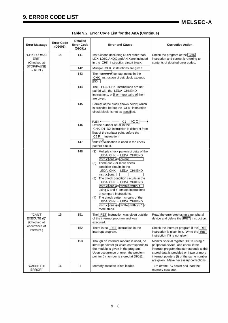
9. ERROR CODE LIST
9 − 8
MELSEC-A
Table 9.2 Error Code List for the AnA (Continue)
Error Massage Error Code(D9008)
Detailed Error Code
(D9091) Error and Cause Corrective Action
141 Instructions (including NOP) other than LDX, LDIX, ANDX and ANIX are included in the CHK instruction circuit block.
142 Multiple CHK instructions are given.
143 The number of contact points in the CHK instruction circuit block exceeds 150.
144 The LEDA CHK instructions are not paired with the LEDA CHKEND instructions, or 2 or more pairs of them are given.
145 Format of the block shown below, which is provided before the CHK instruction circuit block, is not as specified.
146 Device number of D1 in the CHK D1 D2 instruction is different from that of the contact point before the CJ P instruction.
147 Index qualification is used in the check pattern circuit.
"CHK FORMAT ERR"
(Checked at STOP/PAUSE
→ RUN.)
14
148 (1) Multiple check pattern circuits of the LEDA CHK - LEDA CHKEND instructions are given. (2) There are 7 or more check condition circuits in the LEDA CHK - LEDA CHKEND instructions. (3) The check condition circuits in the LEDA CHK - LEDA CHKEND instructions are written without using X and Y contact instructions or compare instructions. (4) The check pattern circuits of the LEDA CHK - LEDA CHKEND instructions are written with 257 or more steps.
Check the program of the CHK instruction and correct it referring to contents of detailed error codes.
151 The IRET instruction was given outside of the interrupt program and was executed.
Read the error step using a peripheral device and delete the IRET instruction.
152 There is no IRET instruction in the interrupt program.
Check the interrupt program if the IRET instruction is given in it. Write the IRET instruction if it is not given.
"CAN'T EXECUTE (I)" (Checked at
occurrence of interrupt.)
15
153 Though an interrupt module is used, no interrupt pointer (I) which corresponds to the module is given in the program. Upon occurrence of error, the problem pointer (I) number is stored at D9011.
Monitor special register D9011 using a peripheral device, and check if the interrupt program that corresponds to the stored data is provided or if two or more interrupt pointers (I) of the same number are given. Make necessary corrections.
"CASSETTE ERROR"
16 Memory cassette is not loaded. Turn off the PC power and load the memory cassette.
P254 CJ P
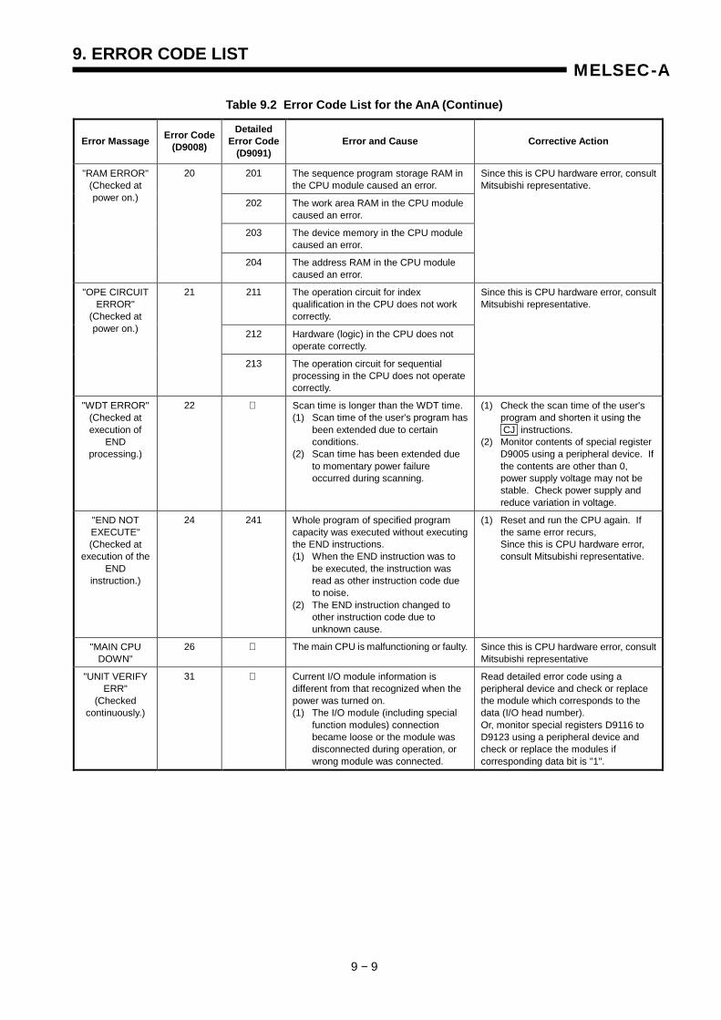
9. ERROR CODE LIST
9 − 9
MELSEC-A
Table 9.2 Error Code List for the AnA (Continue)
Error Massage Error Code(D9008)
Detailed Error Code
(D9091) Error and Cause Corrective Action
201 The sequence program storage RAM in the CPU module caused an error.
202 The work area RAM in the CPU module caused an error.
203 The device memory in the CPU module caused an error.
"RAM ERROR" (Checked at power on.)
20
204 The address RAM in the CPU module caused an error.
Since this is CPU hardware error, consult Mitsubishi representative.
211 The operation circuit for index qualification in the CPU does not work correctly.
212 Hardware (logic) in the CPU does not operate correctly.
"OPE CIRCUIT ERROR"
(Checked at power on.)
21
213 The operation circuit for sequential processing in the CPU does not operate correctly.
Since this is CPU hardware error, consult Mitsubishi representative.
"WDT ERROR" (Checked at execution of
END processing.)
22 Scan time is longer than the WDT time. (1) Scan time of the user's program has been extended due to certain conditions. (2) Scan time has been extended due to momentary power failure occurred during scanning.
(1) Check the scan time of the user's program and shorten it using the CJ instructions. (2) Monitor contents of special register D9005 using a peripheral device. If the contents are other than 0, power supply voltage may not be stable. Check power supply and reduce variation in voltage.
"END NOT EXECUTE" (Checked at
execution of the END
instruction.)
24 241 Whole program of specified program capacity was executed without executing the END instructions. (1) When the END instruction was to be executed, the instruction was read as other instruction code due to noise. (2) The END instruction changed to other instruction code due to unknown cause.
(1) Reset and run the CPU again. If the same error recurs, Since this is CPU hardware error, consult Mitsubishi representative.
"MAIN CPU DOWN"
26 The main CPU is malfunctioning or faulty. Since this is CPU hardware error, consult Mitsubishi representative
"UNIT VERIFY ERR"
(Checked continuously.)
31 Current I/O module information is different from that recognized when the power was turned on. (1) The I/O module (including special function modules) connection became loose or the module was disconnected during operation, or wrong module was connected.
Read detailed error code using a peripheral device and check or replace the module which corresponds to the data (I/O head number). Or, monitor special registers D9116 to D9123 using a peripheral device and check or replace the modules if corresponding data bit is "1".
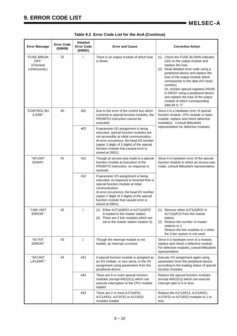
9. ERROR CODE LIST
9 − 10
MELSEC-A
Table 9.2 Error Code List for the AnA (Continue)
Error Massage Error Code(D9008)
Detailed Error Code
(D9091) Error and Cause Corrective Action
"FUSE BREAK OFF"
(Checked continuously.)
32 There is an output module of which fuse is blown.
(1) Check the FUSE BLOWN indicator LED on the output module and replace the fuse. (2) Read detailed error code using a peripheral device and replace the fuse of the output module which corresponds to the data (I/O head number). Or, monitor special registers D9100 to D9107 using a peripheral device and replace the fuse of the output module of which corresponding data bit is "1".
401 Due to the error of the control bus which connects to special function modules, the FROM/TO instruction cannot be executed.
"CONTROL-BUS ERR"
40
402 If parameter I/O assignment is being executed, special function modules are not accessible at initial communication. At error occurrence, the head I/O number (upper 2 digits of 3 digits) of the special function module that caused error is stored at D9011.
Since it is a hardware error of special function module, CPU module or base module, replace and check defective module(s). Consult Mitsubishi representative for defective modules.
411 Though an access was made to a special function module at execution of the FROM/TO instruction, no response is received.
"SP.UNIT DOWN"
41
412 If parameter I/O assignment is being executed, no response is received from a special function module at initial communication. At error occurrence, the head I/O number (upper 2 digits of 3 digits) of the special function module that caused error is stored at D9011.
Since it is hardware error of the special function module to which an access was made, consult Mitsubishi representative.
"LINK UNIT ERROR"
42 (1) Either AJ71(A)R22 or AJ71(A)P22 is loaded to the master station. (2) There are 2 link modules which are set to the master station (station 0).
(1) Remove either AJ71(A)R22 or AJ71(A)P22 from the master station. (2) Reduce the number of master stations to 1. Reduce the link modules to 1 when the 3-tier system is not used.
"I/O INT. ERROR"
43 Though the interrupt module is not loaded, an interrupt occurred.
Since it is hardware error of a module, replace and check a defective module. For defective modules, consult Mitsubishi representative.
441 A special function module is assigned as an I/O module, or vice versa, in the I/O assignment using parameters from the peripheral device.
Execute I/O assignment again using parameters from the peripheral device according to the loading status of special function modules.
442 There are 9 or more special function modules (except AI61(S1)) which can execute interruption to the CPU module loaded.
Reduce the special function modules (except AI61(S1)) which can execute interrupt start to 8 or less.
"SP.UNIT LAY.ERR."
44
443 There are 2 or more AJ71AP21, AJ71AR21, AJ71P22 or AJ71R22 modules loaded.
Reduce the AJ71AP21, AJ71AR21, AJ71P22 or AJ71R22 modules to 1 or less.
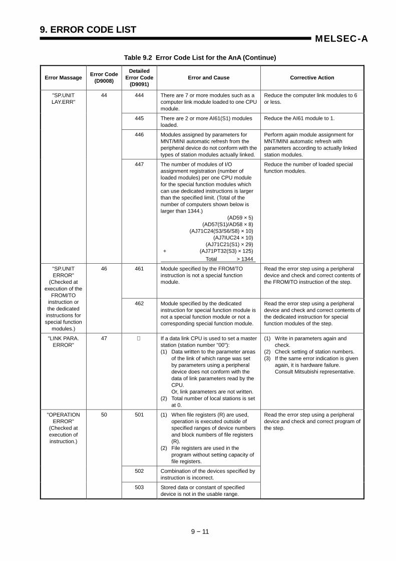
9. ERROR CODE LIST
9 − 11
MELSEC-A
Table 9.2 Error Code List for the AnA (Continue)
Error Massage Error Code(D9008)
Detailed Error Code
(D9091) Error and Cause Corrective Action
444 There are 7 or more modules such as a computer link module loaded to one CPU module.
Reduce the computer link modules to 6 or less.
445 There are 2 or more AI61(S1) modules loaded.
Reduce the AI61 module to 1.
446 Modules assigned by parameters for MNT/MINI automatic refresh from the peripheral device do not conform with the types of station modules actually linked.
Perform again module assignment for MNT/MINI automatic refresh with parameters according to actually linked station modules.
"SP.UNIT LAY.ERR"
44
447 The number of modules of I/O assignment registration (number of loaded modules) per one CPU module for the special function modules which can use dedicated instructions is larger than the specified limit. (Total of the number of computers shown below is larger than 1344.)
(AD59 × 5) (AD57(S1)/AD58 × 8)
(AJ71C24(S3/S6/S8) × 10) (AJ7IUC24 × 10)
(AJ71C21(S1) × 29) + (AJ71PT32(S3) × 125)
Total > 1344
Reduce the number of loaded special function modules.
461 Module specified by the FROM/TO instruction is not a special function module.
Read the error step using a peripheral device and check and correct contents of the FROM/TO instruction of the step.
"SP.UNIT ERROR"
(Checked at execution of the
FROM/TO instruction or the dedicated instructions for special function
modules.)
46
462 Module specified by the dedicated instruction for special function module is not a special function module or not a corresponding special function module.
Read the error step using a peripheral device and check and correct contents of the dedicated instruction for special function modules of the step.
"LINK PARA. ERROR"
47 If a data link CPU is used to set a master station (station number "00"): (1) Data written to the parameter areas of the link of which range was set by parameters using a peripheral device does not conform with the data of link parameters read by the CPU. Or, link parameters are not written. (2) Total number of local stations is set at 0.
(1) Write in parameters again and check. (2) Check setting of station numbers. (3) If the same error indication is given again, it is hardware failure. Consult Mitsubishi representative.
501 (1) When file registers (R) are used, operation is executed outside of specified ranges of device numbers and block numbers of file registers (R). (2) File registers are used in the program without setting capacity of file registers.
502 Combination of the devices specified by instruction is incorrect.
"OPERATION ERROR"
(Checked at execution of instruction.)
50
503 Stored data or constant of specified device is not in the usable range.
Read the error step using a peripheral device and check and correct program of the step.
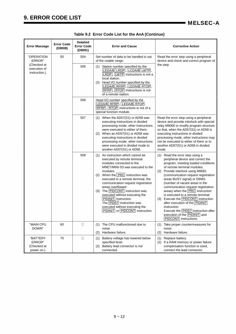
9. ERROR CODE LIST
9 − 12
MELSEC-A
Table 9.2 Error Code List for the AnA (Continue)
Error Massage Error Code(D9008)
Detailed Error Code
(D9091) Error and Cause Corrective Action
504 Set number of data to be handled is out of the usable range.
505 (1) Station number specified by the LEDA/B LRDP , LCDA/B LWTP , LRDP , LWTP instructions is not a local station. (2) Head I/O number specified by the LEDA/B RFRP , LEDA/B RTOP , RFRP , RTOP instructions is not of a remote station.
506 Head I/O number specified by the LEDA/B RFRP , LEDA/B RTOP , RFRP , RTOP instructions is not of a special function module.
Read the error step using a peripheral device and check and correct program of the step.
507 (1) When the AD57(S1) or AD58 was executing instructions in divided processing mode, other instructions were executed to either of them. (2) When an AD57(S1) or AD58 was executing instructions in divided processing mode, other instructions were executed in divided mode to another AD57(S1) or AD58.
Read the error step using a peripheral device and provide interlock with special relay M9066 or modify program structure so that, when the AD57(S1) or AD58 is executing instructions in divided processing mode, other instructions may not be executed to either of them or to another AD57(S1) or AD58 in divided mode.
"OPERATION ERROR"
(Checked at execution of instruction.)
50
509 (1) An instruction which cannot be executed by remote terminal modules connected to the MNET/MINI-S3 was executed to the modules. (2) When the PRC instruction was executed to a remote terminal, the communication request registration areas overflowed. (3) The PIDCONT instruction was executed without executing the PIDINIT instruction. The PID57 instruction was executed without executing the PIDINIT or PIDCONT instruction.
(1) Read the error step using a peripheral device and correct the program, meeting loaded conditions of remote terminal modules. (2) Provide interlock using M9081 (communication request registration areas BUSY signal) or D9081 (number of vacant areas in the communication request registration areas) when the PRC instruction is executed to a remote terminal. (3) Execute the PIDCONT instruction after execution of the PIDINIT instruction. Execute the PID57 instruction after execution of the PIDINIT and PIDCONT instructions.
"MAIN CPU DOWN"
60 (1) The CPU malfunctioned due to noise. (2) Hardware failure.
(1) Take proper countermeasures for noise. (2) Hardware failure.
"BATTERY ERROR"
(Checked at power on.)
70 (1) Battery voltage has lowered below specified level. (2) Battery lead connector is not connected.
(1) Replace battery. (2) If a RAM memory or power failure compensation function is used, connect the lead connector.
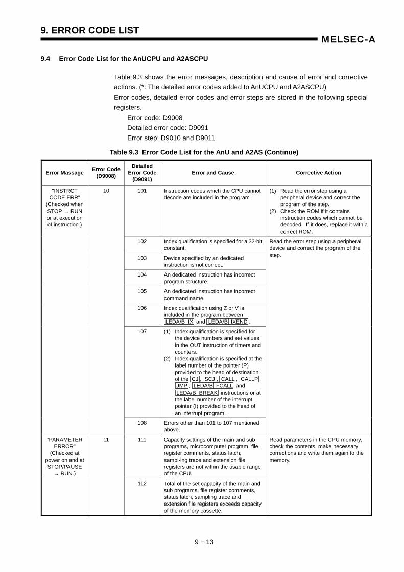
9. ERROR CODE LIST
9 − 13
MELSEC-A
9.4 Error Code List for the AnUCPU and A2ASCPU
Table 9.3 shows the error messages, description and cause of error and corrective actions. (*: The detailed error codes added to AnUCPU and A2ASCPU) Error codes, detailed error codes and error steps are stored in the following special registers. Error code: D9008 Detailed error code: D9091 Error step: D9010 and D9011
Table 9.3 Error Code List for the AnU and A2AS (Continue)
Error Massage Error Code(D9008)
Detailed Error Code
(D9091) Error and Cause Corrective Action
101 Instruction codes which the CPU cannot decode are included in the program.
(1) Read the error step using a peripheral device and correct the program of the step. (2) Check the ROM if it contains instruction codes which cannot be decoded. If it does, replace it with a correct ROM.
102 Index qualification is specified for a 32-bit constant.
103 Device specified by an dedicated instruction is not correct.
104 An dedicated instruction has incorrect program structure.
105 An dedicated instruction has incorrect command name.
106 Index qualification using Z or V is included in the program between LEDA/B IX and LEDA/B IXEND .
107 (1) Index qualification is specified for the device numbers and set values in the OUT instruction of timers and counters. (2) Index qualification is specified at the label number of the pointer (P) provided to the head of destination of the CJ , SCJ , CALL , CALLP , JMP , LEDA/B FCALL and LEDA/B BREAK instructions or at the label number of the interrupt pointer (I) provided to the head of an interrupt program.
"INSTRCT CODE ERR"
(Checked when STOP → RUN or at execution of instruction.)
10
108 Errors other than 101 to 107 mentioned above.
Read the error step using a peripheral device and correct the program of the step.
111 Capacity settings of the main and sub programs, microcomputer program, file register comments, status latch, sampl-ing trace and extension file registers are not within the usable range of the CPU.
"PARAMETER ERROR"
(Checked at power on and at STOP/PAUSE
→ RUN.)
11
112 Total of the set capacity of the main and sub programs, file register comments, status latch, sampling trace and extension file registers exceeds capacity of the memory cassette.
Read parameters in the CPU memory, check the contents, make necessary corrections and write them again to the memory.
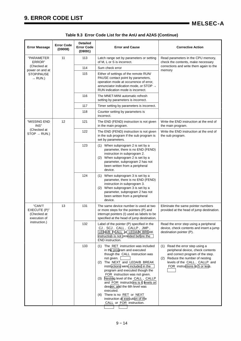
9. ERROR CODE LIST
9 − 14
MELSEC-A
Table 9.3 Error Code List for the AnU and A2AS (Continue)
Error Massage Error Code(D9008)
Detailed Error Code
(D9091) Error and Cause Corrective Action
113 Latch range set by parameters or setting of M, L or S is incorrect.
114 Sum check error
115 Either of settings of the remote RUN/ PAUSE contact point by parameters, operation mode at occurrence of error, annunciator indication mode, or STOP → RUN indication mode is incorrect.
116 The MNET-MINI automatic refresh setting by parameters is incorrect.
117 Timer setting by parameters is incorrect.
"PARAMETER ERROR"
(Checked at power on and at STOP/PAUSE
→ RUN.)
11
118 Counter setting by parameters is incorrect.
Read parameters in the CPU memory, check the contents, make necessary corrections and write them again to the memory
121 The END (FEND) instruction is not given in the main program.
Write the END instruction at the end of the main program.
122 The END (FEND) instruction is not given in the sub program if the sub program is set by parameters.
123 (1) When subprogram 2 is set by a parameter, there is no END (FEND) instruction in subprogram 2. (2) When subprogram 2 is set by a parameter, subprogram 2 has not been written from a peripheral device.
"MISSING END INS"
(Checked at STOP → RUN.)
12
124 (1) When subprogram 3 is set by a parameter, there is no END (FEND) instruction in subprogram 3. (2) When subprogram 3 is set by a parameter, subprogram 2 has not been written from a peripheral device.
Write the END instruction at the end of the sub program.
131 The same device number is used at two or more steps for the pointers (P) and interrupt pointers (I) used as labels to be specified at the head of jump destination.
Eliminate the same pointer numbers provided at the head of jump destination.
132 Label of the pointer (P) specified in the CJ , SCJ , CALL , CALLP , JMP , LEDA/B FCALL or LEDA/B BREAK instruction is not provided before the END instruction.
Read the error step using a peripheral device, check contents and insert a jump destination pointer (P).
"CAN'T EXECUTE (P)"
(Checked at execution of instruction.)
13
133 (1) The RET instruction was included in the program and executed though the CALL instruction was not given. (2) The NEXT and LEDA/B BREAK instructions were included in the program and executed though the FOR instruction was not given. (3) Nesting level of the CALL , CALLP and FOR instructions is 6 levels or deeper, and the 6th level was executed. (4) There is no RET or NEXT instruction at execution of the CALL or FOR instruction.
(1) Read the error step using a peripheral device, check contents and correct program of the step. (2) Reduce the number of nesting levels of the CALL , CALLP and FOR instructions to 5 or less.

9. ERROR CODE LIST
9 − 15
MELSEC-A
Table 9.3 Error Code List for the AnU and A2AS (Continue)
Error Massage Error Code(D9008)
Detailed Error Code
(D9091) Error and Cause Corrective Action
134 The CHG instruction was included in the program and executed though no sub program was provided.
Read the error step using a peripheral device and delete the CHG instruction circuit block.
"CAN'T EXECUTE (P)"
(Checked at execution of instruction.)
13
135 (1) LEDA/B IX and LEDA IXEND instructions are not paired. (2) There are 33 or more sets of LEDA/B IX and LEDA IXEND instructions.
(1) Read the error step using a peripheral device, check contents and correct program of the step. (2) Reduce the number of sets of LEDA/B IX and LEDA IXEND instructions to 32 or less.
141 Instructions (including NOP) other than LDX, LDIX, ANDX and ANIX are included in the CHK instruction circuit block.
142 Multiple CHK instructions are given.
143 The number of contact points in the CHK instruction circuit block exceeds 150.
144 The LEDA CHK instructions are not paired with the LEDA CHKEND instructions, or 2 or more pairs of them are given.
145 Format of the block shown below, which is provided before the CHK instruction circuit block, is not as specified.
146 Device number of D1 in the CHK D1 D2 instruction is different from that of the contact point before the CJ P instruction.
147 Index qualification is used in the check pattern circuit.
"CHK FORMAT ERR"
(Checked at STOP/PAUSE
→ RUN.)
14
148 (1) Multiple check pattern circuits of the LEDA CHK - LEDA CHKEND instructions are given. (2) There are 7 or more check condition circuits in the LEDA CHK - LEDA CHKEND instructions. (3) The check condition circuits in the LEDA CHK - LEDA CHKEND instructions are written without using X and Y contact instructions or compare instructions. (4) The check pattern circuits of the LEDA CHK - LEDA CHKEND instructions are written with 257 or more steps.
Check the program of the CHK instruction and correct it referring to contents of detailed error codes.
151 The IRET instruction was given outside of the interrupt program and was executed.
Read the error step using a peripheral device and delete the IRET instruction.
"CAN'T EXECUTE (I)" (Checked at
occurrence of interrupt.)
15
152 There is no IRET instruction in the interrupt program.
Check the interrupt program if the IRET instruction is given in it. Write the IRET instruction if it is not given.
P254 CJ P
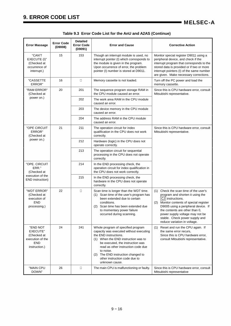
9. ERROR CODE LIST
9 − 16
MELSEC-A
Table 9.3 Error Code List for the AnU and A2AS (Continue)
Error Massage Error Code(D9008)
Detailed Error Code
(D9091) Error and Cause Corrective Action
"CAN'T EXECUTE (I)" (Checked at
occurrence of interrupt.)
15 153 Though an interrupt module is used, no interrupt pointer (I) which corresponds to the module is given in the program. Upon occurrence of error, the problem pointer (I) number is stored at D9011.
Monitor special register D9011 using a peripheral device, and check if the interrupt program that corresponds to the stored data is provided or if two or more interrupt pointers (I) of the same number are given. Make necessary corrections.
"CASSETTE ERROR"
16 Memory cassette is not loaded. Turn off the PC power and load the memory cassette.
201 The sequence program storage RAM in the CPU module caused an error.
202 The work area RAM in the CPU module caused an error.
203 The device memory in the CPU module caused an error.
"RAM ERROR" (Checked at power on.)
20
204 The address RAM in the CPU module caused an error.
Since this is CPU hardware error, consult Mitsubishi representative.
211 The operation circuit for index qualification in the CPU does not work correctly.
212 Hardware (logic) in the CPU does not operate correctly.
"OPE CIRCUIT ERROR"
(Checked at power on.)
213 The operation circuit for sequential processing in the CPU does not operate correctly.
Since this is CPU hardware error, consult Mitsubishi representative.
214 In the END processing check, the operation circuit for index qualification in the CPU does not work correctly.
"OPE. CIRCUIT ERR."
(Checked at execution of the END instruction)
21
215 In the END processing check, the hardware in the CPU does not operate correctly.
"WDT ERROR" (Checked at execution of
END processing.)
22 Scan time is longer than the WDT time. (1) Scan time of the user's program has been extended due to certain conditions. (2) Scan time has been extended due to momentary power failure occurred during scanning.
(1) Check the scan time of the user's program and shorten it using the CJ instructions. (2) Monitor contents of special register D9005 using a peripheral device. If the contents are other than 0, power supply voltage may not be stable. Check power supply and reduce variation in voltage.
"END NOT EXECUTE" (Checked at
execution of the END
instruction.)
24 241 Whole program of specified program capacity was executed without executing the END instructions. (1) When the END instruction was to be executed, the instruction was read as other instruction code due to noise. (2) The END instruction changed to other instruction code due to unknown cause.
(1) Reset and run the CPU again. If the same error recurs, Since this is CPU hardware error, consult Mitsubishi representative.
"MAIN CPU DOWN"
26 The main CPU is malfunctioning or faulty. Since this is CPU hardware error, consult Mitsubishi representative
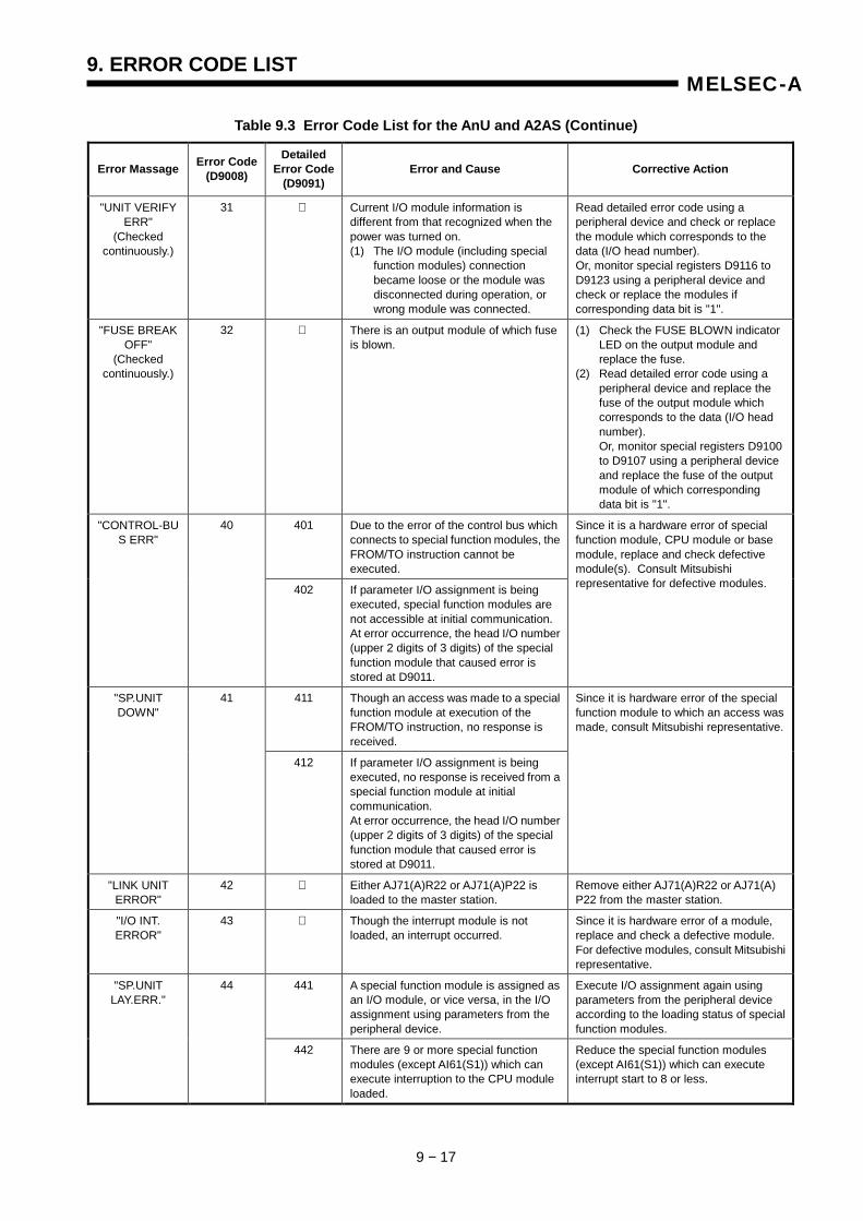
9. ERROR CODE LIST
9 − 17
MELSEC-A
Table 9.3 Error Code List for the AnU and A2AS (Continue)
Error Massage Error Code(D9008)
Detailed Error Code
(D9091) Error and Cause Corrective Action
"UNIT VERIFY ERR"
(Checked continuously.)
31 Current I/O module information is different from that recognized when the power was turned on. (1) The I/O module (including special function modules) connection became loose or the module was disconnected during operation, or wrong module was connected.
Read detailed error code using a peripheral device and check or replace the module which corresponds to the data (I/O head number). Or, monitor special registers D9116 to D9123 using a peripheral device and check or replace the modules if corresponding data bit is "1".
"FUSE BREAK OFF"
(Checked continuously.)
32 There is an output module of which fuse is blown.
(1) Check the FUSE BLOWN indicator LED on the output module and replace the fuse. (2) Read detailed error code using a peripheral device and replace the fuse of the output module which corresponds to the data (I/O head number). Or, monitor special registers D9100 to D9107 using a peripheral device and replace the fuse of the output module of which corresponding data bit is "1".
401 Due to the error of the control bus which connects to special function modules, the FROM/TO instruction cannot be executed.
"CONTROL-BUS ERR"
40
402 If parameter I/O assignment is being executed, special function modules are not accessible at initial communication. At error occurrence, the head I/O number (upper 2 digits of 3 digits) of the special function module that caused error is stored at D9011.
Since it is a hardware error of special function module, CPU module or base module, replace and check defective module(s). Consult Mitsubishi representative for defective modules.
411 Though an access was made to a special function module at execution of the FROM/TO instruction, no response is received.
"SP.UNIT DOWN"
41
412 If parameter I/O assignment is being executed, no response is received from a special function module at initial communication. At error occurrence, the head I/O number (upper 2 digits of 3 digits) of the special function module that caused error is stored at D9011.
Since it is hardware error of the special function module to which an access was made, consult Mitsubishi representative.
"LINK UNIT ERROR"
42 Either AJ71(A)R22 or AJ71(A)P22 is loaded to the master station.
Remove either AJ71(A)R22 or AJ71(A) P22 from the master station.
"I/O INT. ERROR"
43 Though the interrupt module is not loaded, an interrupt occurred.
Since it is hardware error of a module, replace and check a defective module. For defective modules, consult Mitsubishi representative.
441 A special function module is assigned as an I/O module, or vice versa, in the I/O assignment using parameters from the peripheral device.
Execute I/O assignment again using parameters from the peripheral device according to the loading status of special function modules.
"SP.UNIT LAY.ERR."
44
442 There are 9 or more special function modules (except AI61(S1)) which can execute interruption to the CPU module loaded.
Reduce the special function modules (except AI61(S1)) which can execute interrupt start to 8 or less.
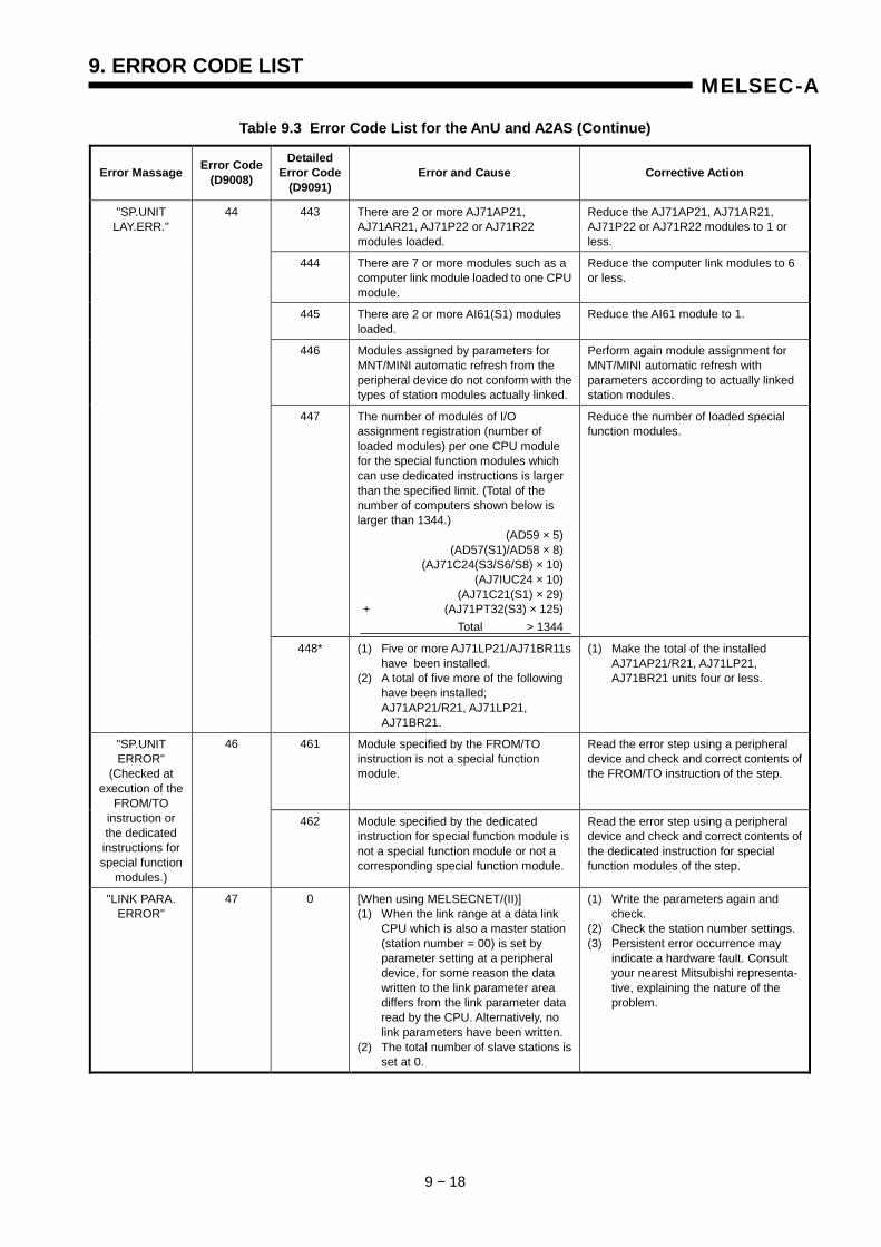
9. ERROR CODE LIST
9 − 18
MELSEC-A
Table 9.3 Error Code List for the AnU and A2AS (Continue)
Error Massage Error Code(D9008)
Detailed Error Code
(D9091) Error and Cause Corrective Action
443 There are 2 or more AJ71AP21, AJ71AR21, AJ71P22 or AJ71R22 modules loaded.
Reduce the AJ71AP21, AJ71AR21, AJ71P22 or AJ71R22 modules to 1 or less.
444 There are 7 or more modules such as a computer link module loaded to one CPU module.
Reduce the computer link modules to 6 or less.
445 There are 2 or more AI61(S1) modules loaded.
Reduce the AI61 module to 1.
446 Modules assigned by parameters for MNT/MINI automatic refresh from the peripheral device do not conform with the types of station modules actually linked.
Perform again module assignment for MNT/MINI automatic refresh with parameters according to actually linked station modules.
447 The number of modules of I/O assignment registration (number of loaded modules) per one CPU module for the special function modules which can use dedicated instructions is larger than the specified limit. (Total of the number of computers shown below is larger than 1344.)
(AD59 × 5) (AD57(S1)/AD58 × 8)
(AJ71C24(S3/S6/S8) × 10) (AJ7IUC24 × 10)
(AJ71C21(S1) × 29) + (AJ71PT32(S3) × 125)
Total > 1344
Reduce the number of loaded special function modules.
"SP.UNIT LAY.ERR."
44
448* (1) Five or more AJ71LP21/AJ71BR11s have been installed. (2) A total of five more of the following have been installed; AJ71AP21/R21, AJ71LP21, AJ71BR21.
(1) Make the total of the installed AJ71AP21/R21, AJ71LP21, AJ71BR21 units four or less.
461 Module specified by the FROM/TO instruction is not a special function module.
Read the error step using a peripheral device and check and correct contents of the FROM/TO instruction of the step.
"SP.UNIT ERROR"
(Checked at execution of the
FROM/TO instruction or the dedicated instructions for special function
modules.)
46
462 Module specified by the dedicated instruction for special function module is not a special function module or not a corresponding special function module.
Read the error step using a peripheral device and check and correct contents of the dedicated instruction for special function modules of the step.
"LINK PARA. ERROR"
47 0 [When using MELSECNET/(II)] (1) When the link range at a data link CPU which is also a master station (station number = 00) is set by parameter setting at a peripheral device, for some reason the data written to the link parameter area differs from the link parameter data read by the CPU. Alternatively, no link parameters have been written. (2) The total number of slave stations is set at 0.
(1) Write the parameters again and check. (2) Check the station number settings. (3) Persistent error occurrence may indicate a hardware fault. Consult your nearest Mitsubishi representa- tive, explaining the nature of the problem.
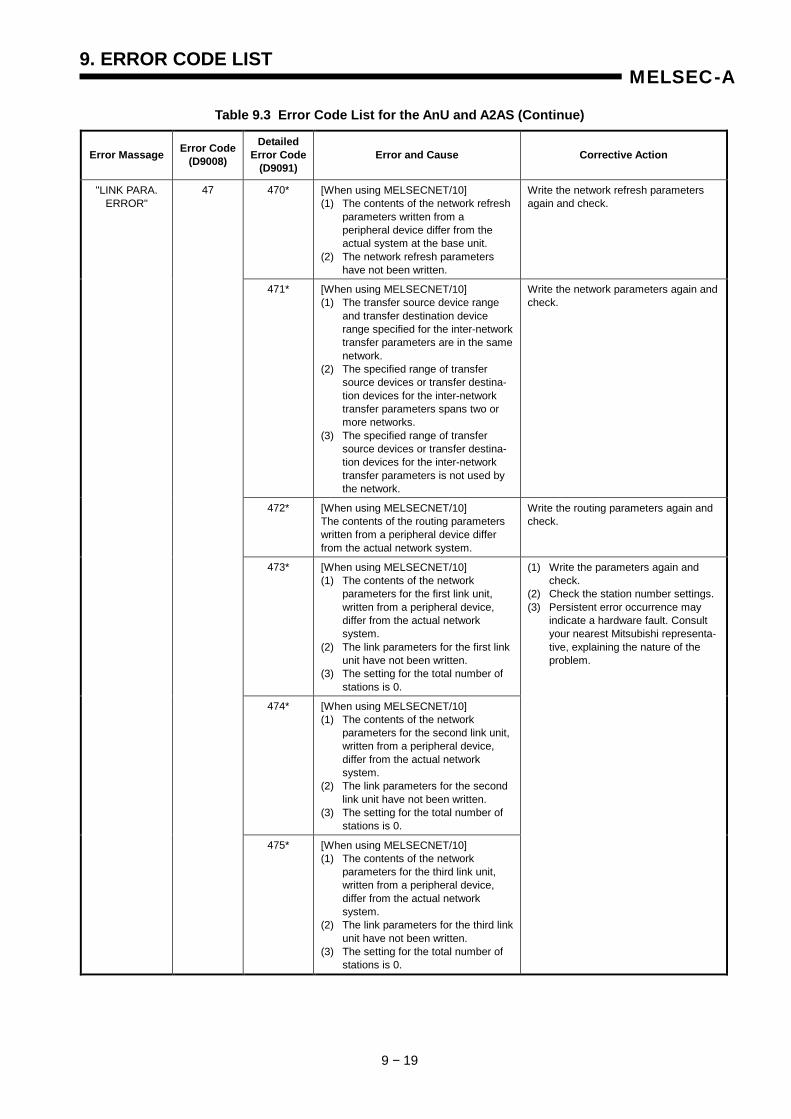
9. ERROR CODE LIST
9 − 19
MELSEC-A
Table 9.3 Error Code List for the AnU and A2AS (Continue)
Error Massage Error Code(D9008)
Detailed Error Code
(D9091) Error and Cause Corrective Action
470* [When using MELSECNET/10] (1) The contents of the network refresh parameters written from a peripheral device differ from the actual system at the base unit. (2) The network refresh parameters have not been written.
Write the network refresh parameters again and check.
471* [When using MELSECNET/10] (1) The transfer source device range and transfer destination device range specified for the inter-network transfer parameters are in the same network. (2) The specified range of transfer source devices or transfer destina- tion devices for the inter-network transfer parameters spans two or more networks. (3) The specified range of transfer source devices or transfer destina- tion devices for the inter-network transfer parameters is not used by the network.
Write the network parameters again and check.
472* [When using MELSECNET/10] The contents of the routing parameters written from a peripheral device differ from the actual network system.
Write the routing parameters again and check.
473* [When using MELSECNET/10] (1) The contents of the network parameters for the first link unit, written from a peripheral device, differ from the actual network system. (2) The link parameters for the first link unit have not been written. (3) The setting for the total number of stations is 0.
474* [When using MELSECNET/10] (1) The contents of the network parameters for the second link unit, written from a peripheral device, differ from the actual network system. (2) The link parameters for the second link unit have not been written. (3) The setting for the total number of stations is 0.
"LINK PARA. ERROR"
47
475* [When using MELSECNET/10] (1) The contents of the network parameters for the third link unit, written from a peripheral device, differ from the actual network system. (2) The link parameters for the third link unit have not been written. (3) The setting for the total number of stations is 0.
(1) Write the parameters again and check. (2) Check the station number settings. (3) Persistent error occurrence may indicate a hardware fault. Consult your nearest Mitsubishi representa- tive, explaining the nature of the problem.
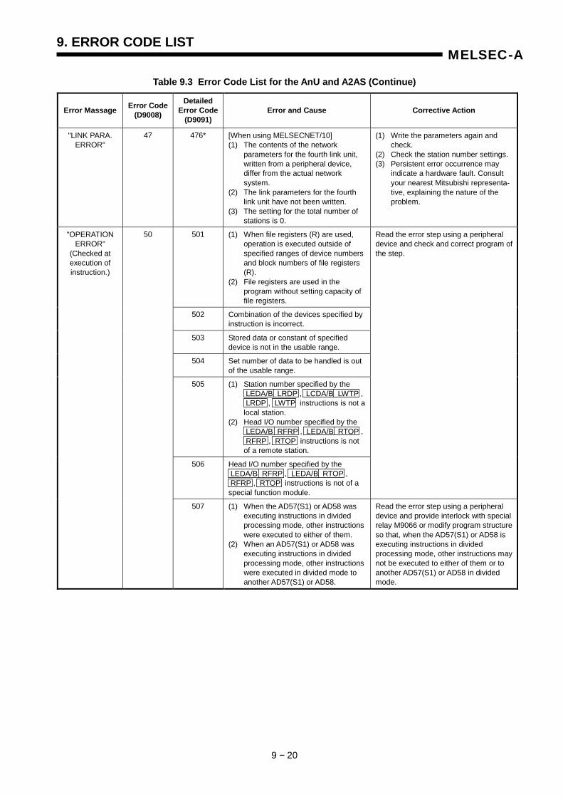
9. ERROR CODE LIST
9 − 20
MELSEC-A
Table 9.3 Error Code List for the AnU and A2AS (Continue)
Error Massage Error Code(D9008)
Detailed Error Code
(D9091) Error and Cause Corrective Action
"LINK PARA. ERROR"
47 476* [When using MELSECNET/10] (1) The contents of the network parameters for the fourth link unit, written from a peripheral device, differ from the actual network system. (2) The link parameters for the fourth link unit have not been written. (3) The setting for the total number of stations is 0.
(1) Write the parameters again and check. (2) Check the station number settings. (3) Persistent error occurrence may indicate a hardware fault. Consult your nearest Mitsubishi representa- tive, explaining the nature of the problem.
501 (1) When file registers (R) are used, operation is executed outside of specified ranges of device numbers and block numbers of file registers (R). (2) File registers are used in the program without setting capacity of file registers.
502 Combination of the devices specified by instruction is incorrect.
503 Stored data or constant of specified device is not in the usable range.
504 Set number of data to be handled is out of the usable range.
505 (1) Station number specified by the LEDA/B LRDP , LCDA/B LWTP , LRDP , LWTP instructions is not a local station. (2) Head I/O number specified by the LEDA/B RFRP , LEDA/B RTOP , RFRP , RTOP instructions is not of a remote station.
506 Head I/O number specified by the LEDA/B RFRP , LEDA/B RTOP , RFRP , RTOP instructions is not of a special function module.
Read the error step using a peripheral device and check and correct program of the step.
"OPERATION ERROR"
(Checked at execution of instruction.)
50
507 (1) When the AD57(S1) or AD58 was executing instructions in divided processing mode, other instructions were executed to either of them. (2) When an AD57(S1) or AD58 was executing instructions in divided processing mode, other instructions were executed in divided mode to another AD57(S1) or AD58.
Read the error step using a peripheral device and provide interlock with special relay M9066 or modify program structure so that, when the AD57(S1) or AD58 is executing instructions in divided processing mode, other instructions may not be executed to either of them or to another AD57(S1) or AD58 in divided mode.
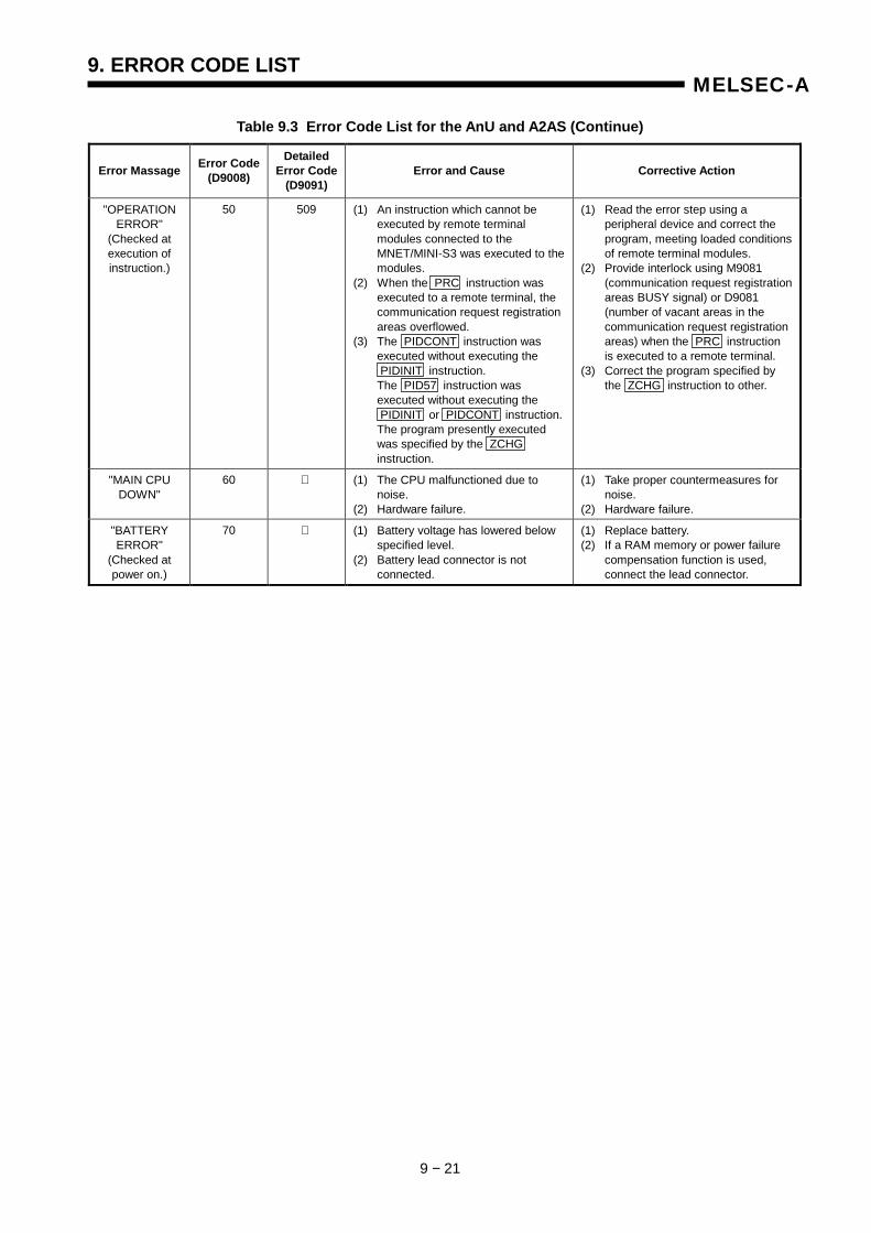
9. ERROR CODE LIST
9 − 21
MELSEC-A
Table 9.3 Error Code List for the AnU and A2AS (Continue)
Error Massage Error Code(D9008)
Detailed Error Code
(D9091) Error and Cause Corrective Action
"OPERATION ERROR"
(Checked at execution of instruction.)
50 509 (1) An instruction which cannot be executed by remote terminal modules connected to the MNET/MINI-S3 was executed to the modules. (2) When the PRC instruction was executed to a remote terminal, the communication request registration areas overflowed. (3) The PIDCONT instruction was executed without executing the PIDINIT instruction. The PID57 instruction was executed without executing the PIDINIT or PIDCONT instruction. The program presently executed was specified by the ZCHG instruction.
(1) Read the error step using a peripheral device and correct the program, meeting loaded conditions of remote terminal modules. (2) Provide interlock using M9081 (communication request registration areas BUSY signal) or D9081 (number of vacant areas in the communication request registration areas) when the PRC instruction is executed to a remote terminal. (3) Correct the program specified by the ZCHG instruction to other.
"MAIN CPU DOWN"
60 (1) The CPU malfunctioned due to noise. (2) Hardware failure.
(1) Take proper countermeasures for noise. (2) Hardware failure.
"BATTERY ERROR"
(Checked at power on.)
70 (1) Battery voltage has lowered below specified level. (2) Battery lead connector is not connected.
(1) Replace battery. (2) If a RAM memory or power failure compensation function is used, connect the lead connector.
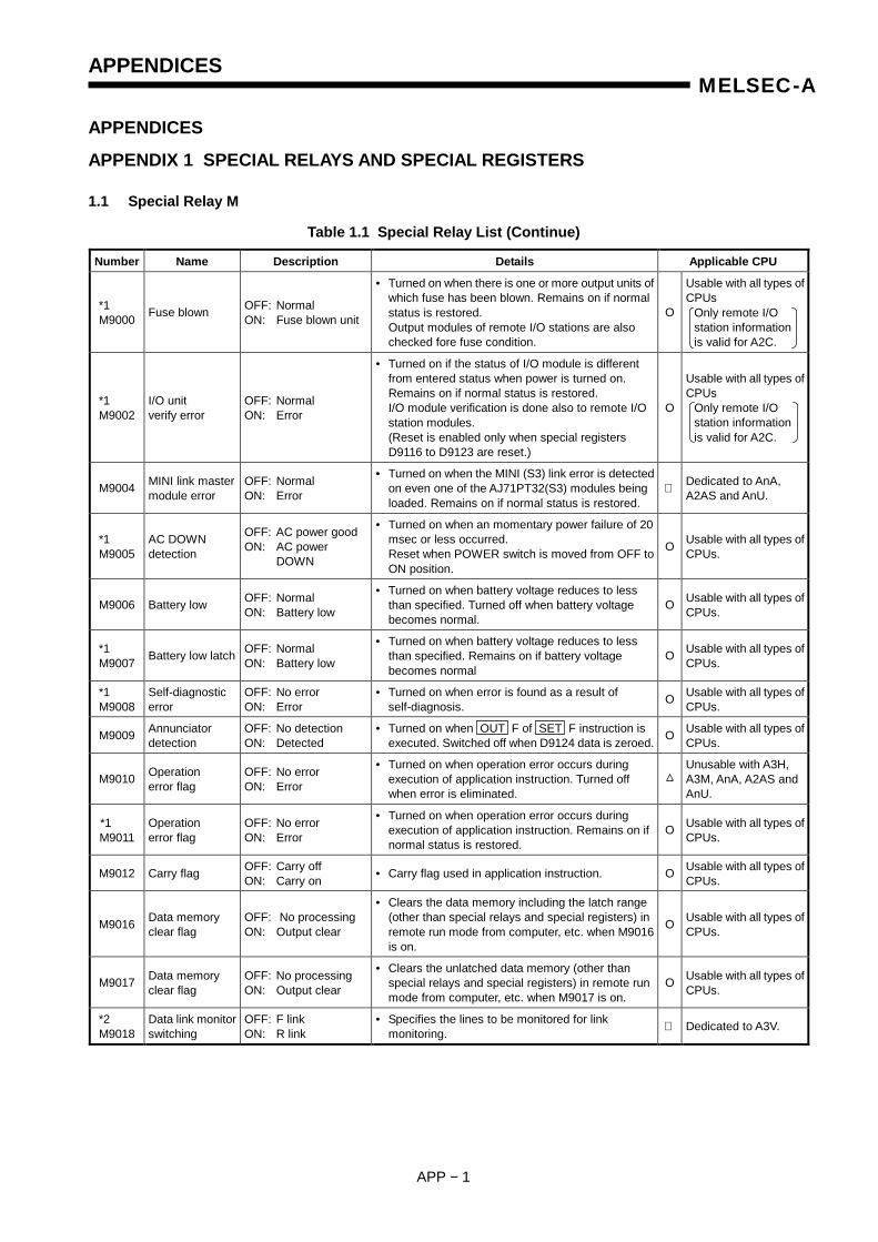
APPENDICES
APP − 1
MELSEC-A
APPENDICES
APPENDIX 1 SPECIAL RELAYS AND SPECIAL REGISTERS
1.1 Special Relay M
Table 1.1 Special Relay List (Continue)
Number Name Description Details Applicable CPU
*1 M9000 Fuse blown OFF: Normal
ON: Fuse blown unit
• Turned on when there is one or more output units of which fuse has been blown. Remains on if normal status is restored. Output modules of remote I/O stations are also checked fore fuse condition.
O
Usable with all types of CPUs Only remote I/O station information is valid for A2C.
*1 M9002
I/O unit verify error
OFF: Normal ON: Error
• Turned on if the status of I/O module is different from entered status when power is turned on. Remains on if normal status is restored. I/O module verification is done also to remote I/O station modules. (Reset is enabled only when special registers D9116 to D9123 are reset.)
O
Usable with all types of CPUs Only remote I/O station information is valid for A2C.
M9004 MINI link master module error
OFF: Normal ON: Error
• Turned on when the MINI (S3) link error is detected on even one of the AJ71PT32(S3) modules being loaded. Remains on if normal status is restored.
Dedicated to AnA, A2AS and AnU.
*1 M9005
AC DOWN detection
OFF: AC power good ON: AC power DOWN
• Turned on when an momentary power failure of 20 msec or less occurred. Reset when POWER switch is moved from OFF to ON position.
O Usable with all types of CPUs.
M9006 Battery low OFF: Normal ON: Battery low
• Turned on when battery voltage reduces to less than specified. Turned off when battery voltage becomes normal.
O Usable with all types of CPUs.
*1 M9007 Battery low latch OFF: Normal
ON: Battery low
• Turned on when battery voltage reduces to less than specified. Remains on if battery voltage becomes normal
O Usable with all types of CPUs.
*1 M9008
Self-diagnostic error
OFF: No error ON: Error
• Turned on when error is found as a result of self-diagnosis. O Usable with all types of
CPUs.
M9009 Annunciator detection
OFF: No detection ON: Detected
• Turned on when OUT F of SET F instruction is executed. Switched off when D9124 data is zeroed. O Usable with all types of
CPUs.
M9010 Operation error flag
OFF: No error ON: Error
• Turned on when operation error occurs during execution of application instruction. Turned off when error is eliminated.
Unusable with A3H, A3M, AnA, A2AS and AnU.
*1 M9011
Operation error flag
OFF: No error ON: Error
• Turned on when operation error occurs during execution of application instruction. Remains on if normal status is restored.
O Usable with all types of CPUs.
M9012 Carry flag OFF: Carry off ON: Carry on • Carry flag used in application instruction. O Usable with all types of
CPUs.
M9016 Data memory clear flag
OFF: No processing ON: Output clear
• Clears the data memory including the latch range (other than special relays and special registers) in remote run mode from computer, etc. when M9016 is on.
O Usable with all types of CPUs.
M9017 Data memory clear flag
OFF: No processing ON: Output clear
• Clears the unlatched data memory (other than special relays and special registers) in remote run mode from computer, etc. when M9017 is on.
O Usable with all types of CPUs.
*2 M9018
Data link monitor switching
OFF: F link ON: R link
• Specifies the lines to be monitored for link monitoring. Dedicated to A3V.
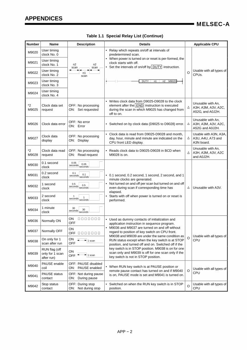
APPENDICES
APP − 2
MELSEC-A
Table 1.1 Special Relay List (Continue)
Number Name Description Details Applicable CPU
M9020 User timing clock No. 0
M9021 User timing clock No. 1
M9022 User timing clock No. 2
M9023 User timing clock No. 3
M9024 User timing clock No. 4
• Relay which repeats on/off at intervals of predetermined scan.
• When power is turned on or reset is per-formed, the clock starts with off.
• Set the intervals of on/off by DUTY instruction. O Usable with all types of
CPUs.
*2 M9025
Clock data set request
OFF: No processing ON: Set requested
• Writes clock data from D9025-D9028 to the clock element after the END instruction is executed during the scan in which M9025 has changed from off to on.
Unusable with An, A3H, A3M, A3V, A2C, A52G, and A0J2H.
M9026 Clock data error OFF: No error ON: Error • Switched on by clock data (D9025 to D9028) error.
Unusable with An, A3H, A3M, A3V, A2C, A52G and A0J2H.
M9027 Clock data display
OFF: No processing ON: Display
• Clock data is read from D9025-D9028 and month, day, hour, minute and minute are indicated on the CPU front LED display.
Usable with A3N, A3A, A3U, A4U, A73 and A3N board.
*2 M9028
Clock data read request
OFF: No processing ON: Read request
• Reads clock data to D9025-D9028 in BCD when M9028 is on.
Unusable with An, A3H, A3M, A3V, A2C and A0J2H.
M9030 0.1 second clock
M9031 0.2 second clock
M9032 1 second clock
M9033 2 second clock
M9034 1 minute clock
• 0.1 second, 0.2 second, 1 second, 2 second, and 1 minute clocks are generated.
• Not turned on and off per scan but turned on and off even during scan if corresponding time has elapsed.
• Starts with off when power is turned on or reset is performed.
Unusable with A3V.
M9036 Normally ON ON OFF
M9037 Normally OFF ON OFF
M9038 On only for 1 scan after run
ON OFF
M9039 RUN flag (off only for 1 scan after run)
ON OFF
• Used as dummy contacts of initialization and application instruction in sequence program.
• M9036 and M9037 are turned on and off without regard to position of key switch on CPU front. M9038 and M9039 are under the same condition as RUN status except when the key switch is at STOP position, and turned off and on. Switched off if the key switch is in STOP position. M9038 is on for one scan only and M9039 is off for one scan only if the key switch is not in STOP position.
O Usable with all types of CPU
M9040 PAUSE enable coil
OFF: PAUSE disabled ON: PAUSE enabled
M9041 PAUSE status contact
OFF: Not during pauseON: During pause
• When RUN key switch is at PAUSE position or remote pause contact has turned on and if M9040 is on, PAUSE mode is set and M9041 is turned on.
O Usable with all types of CPU
M9042 Stop status contact
OFF: During stop ON: Not during stop
• Switched on when the RUN key switch is in STOP position. O Usable with all types of
CPU
0.05 seconds 0.05
seconds
0.1 seconds 0.1
seconds
1 seconds 1
seconds
30 seconds 30
seconds
0.5 seconds 0.5
seconds
1 scan
n2scan
n2 scan
n1 scan
DUTY n1 n2 M9020
1 scan
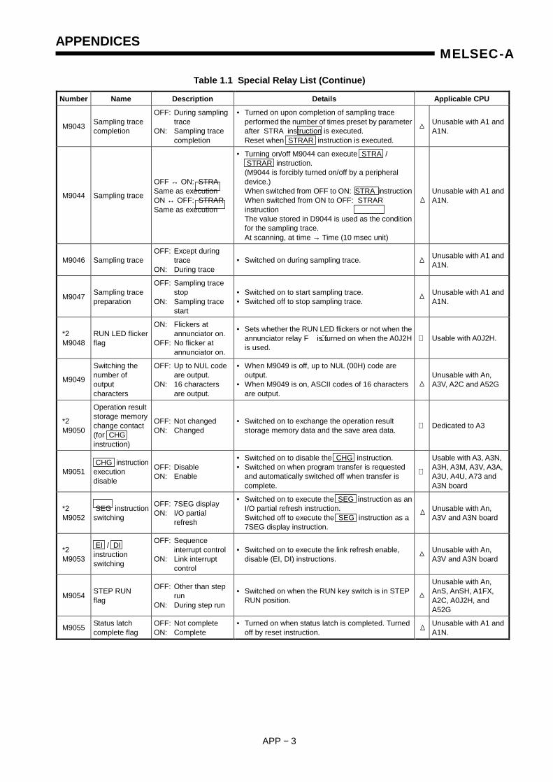
APPENDICES
APP − 3
MELSEC-A
Table 1.1 Special Relay List (Continue)
Number Name Description Details Applicable CPU
M9043 Sampling trace completion
OFF: During sampling trace ON: Sampling trace completion
• Turned on upon completion of sampling trace performed the number of times preset by parameter after STRA instruction is executed. Reset when STRAR instruction is executed.
Unusable with A1 and A1N.
M9044 Sampling trace
OFF ↔ ON: STRA Same as execution ON ↔ OFF: STRAR Same as execution
• Turning on/off M9044 can execute STRA / STRAR instruction. (M9044 is forcibly turned on/off by a peripheral device.) When switched from OFF to ON: STRA instruction When switched from ON to OFF: STRAR instruction The value stored in D9044 is used as the condition for the sampling trace. At scanning, at time → Time (10 msec unit)
Unusable with A1 and A1N.
M9046 Sampling trace OFF: Except during trace ON: During trace
• Switched on during sampling trace. Unusable with A1 and A1N.
M9047 Sampling trace preparation
OFF: Sampling trace stop ON: Sampling trace start
• Switched on to start sampling trace. • Switched off to stop sampling trace. Unusable with A1 and
A1N.
*2 M9048
RUN LED flicker flag
ON: Flickers at annunciator on. OFF: No flicker at annunciator on.
• Sets whether the RUN LED flickers or not when the annunciator relay F is turned on when the A0J2H is used.
Usable with A0J2H.
M9049
Switching the number of output characters
OFF: Up to NUL code are output. ON: 16 characters are output.
• When M9049 is off, up to NUL (00H) code are output.
• When M9049 is on, ASCII codes of 16 characters are output.
Unusable with An, A3V, A2C and A52G
*2 M9050
Operation result storage memory change contact (for CHG instruction)
OFF: Not changed ON: Changed
• Switched on to exchange the operation result storage memory data and the save area data. Dedicated to A3
M9051 CHG instruction execution disable
OFF: Disable ON: Enable
• Switched on to disable the CHG instruction. • Switched on when program transfer is requested
and automatically switched off when transfer is complete.
Usable with A3, A3N, A3H, A3M, A3V, A3A, A3U, A4U, A73 and A3N board
*2 M9052
SEG instruction switching
OFF: 7SEG display ON: I/O partial refresh
• Switched on to execute the SEG instruction as an I/O partial refresh instruction. Switched off to execute the SEG instruction as a 7SEG display instruction.
Unusable with An, A3V and A3N board
*2 M9053
EI / DI instruction switching
OFF: Sequence interrupt control ON: Link interrupt control
• Switched on to execute the link refresh enable, disable (EI, DI) instructions. Unusable with An,
A3V and A3N board
M9054 STEP RUN flag
OFF: Other than step run ON: During step run
• Switched on when the RUN key switch is in STEP RUN position.
Unusable with An, AnS, AnSH, A1FX, A2C, A0J2H, and A52G
M9055 Status latch complete flag
OFF: Not complete ON: Complete
• Turned on when status latch is completed. Turned off by reset instruction. Unusable with A1 and
A1N.
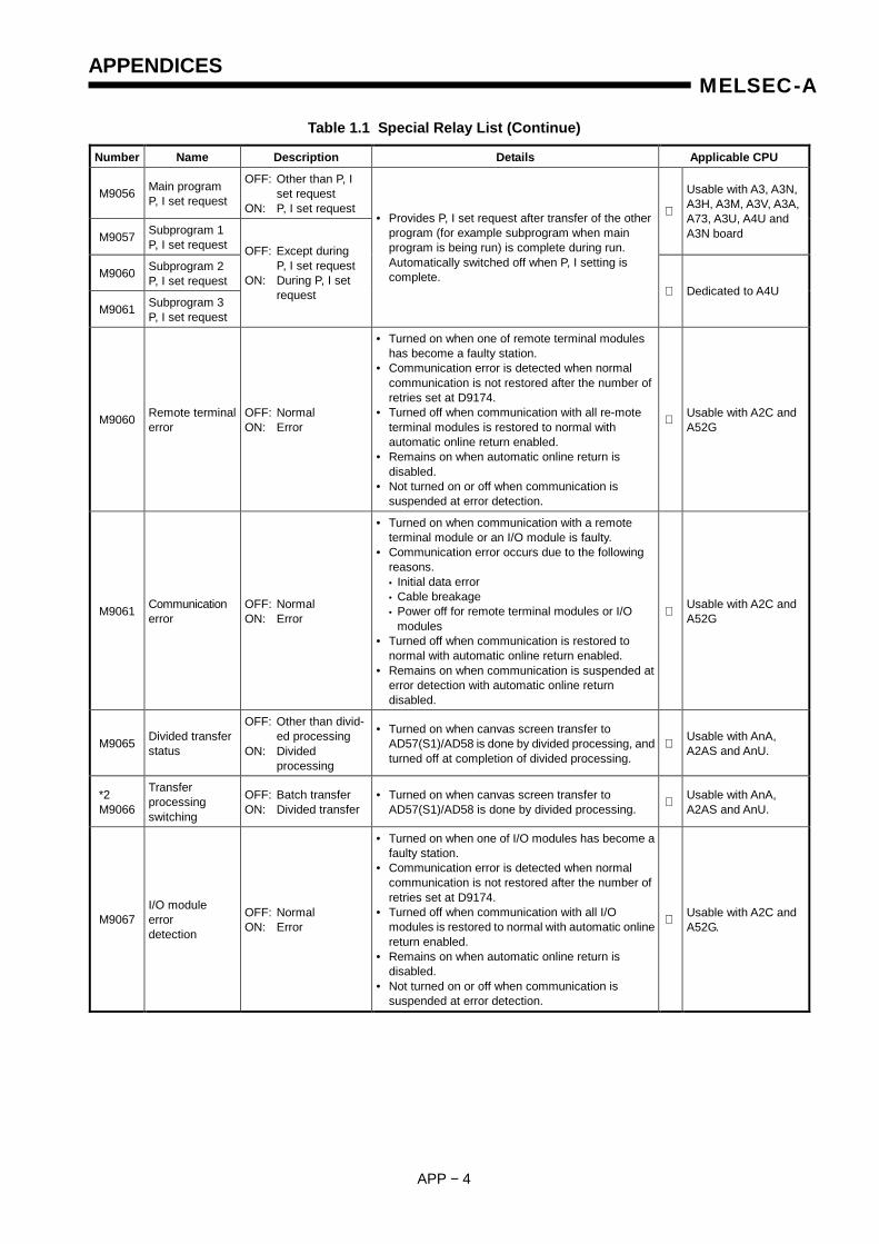
APPENDICES
APP − 4
MELSEC-A
Table 1.1 Special Relay List (Continue)
Number Name Description Details Applicable CPU
M9056 Main program P, I set request
OFF: Other than P, I set request ON: P, I set request
M9057 Subprogram 1 P, I set request
Usable with A3, A3N, A3H, A3M, A3V, A3A, A73, A3U, A4U and A3N board
M9060 Subprogram 2 P, I set request
M9061 Subprogram 3 P, I set request
OFF: Except during P, I set request ON: During P, I set request
• Provides P, I set request after transfer of the other program (for example subprogram when main program is being run) is complete during run. Automatically switched off when P, I setting is complete.
Dedicated to A4U
M9060 Remote terminal error
OFF: Normal ON: Error
• Turned on when one of remote terminal modules has become a faulty station.
• Communication error is detected when normal communication is not restored after the number of retries set at D9174.
• Turned off when communication with all re-mote terminal modules is restored to normal with automatic online return enabled.
• Remains on when automatic online return is disabled.
• Not turned on or off when communication is suspended at error detection.
Usable with A2C and A52G
M9061 Communication error
OFF: Normal ON: Error
• Turned on when communication with a remote terminal module or an I/O module is faulty.
• Communication error occurs due to the following reasons.
• Initial data error • Cable breakage • Power off for remote terminal modules or I/O
modules • Turned off when communication is restored to
normal with automatic online return enabled. • Remains on when communication is suspended at
error detection with automatic online return disabled.
Usable with A2C and A52G
M9065 Divided transfer status
OFF: Other than divid- ed processing ON: Divided processing
• Turned on when canvas screen transfer to AD57(S1)/AD58 is done by divided processing, and turned off at completion of divided processing.
Usable with AnA, A2AS and AnU.
*2 M9066
Transfer processing switching
OFF: Batch transfer ON: Divided transfer
• Turned on when canvas screen transfer to AD57(S1)/AD58 is done by divided processing. Usable with AnA,
A2AS and AnU.
M9067 I/O module error detection
OFF: Normal ON: Error
• Turned on when one of I/O modules has become a faulty station.
• Communication error is detected when normal communication is not restored after the number of retries set at D9174.
• Turned off when communication with all I/O modules is restored to normal with automatic online return enabled.
• Remains on when automatic online return is disabled.
• Not turned on or off when communication is suspended at error detection.
Usable with A2C and A52G.
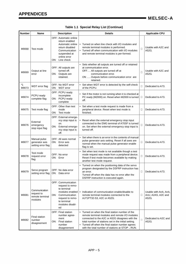
APPENDICES
APP − 5
MELSEC-A
Table 1.1 Special Relay List (Continue)
Number Name Description Details Applicable CPU
M9068 Test mode
OFF: Automatic online return enabled Automatic online return disabled Communication suspended at online error ON: Line check
• Turned on when line check with I/O modules and remote terminal modules is performed.
• Turned off when communication with I/O modules and remote terminal modules is per-formed.
Usable with A2C and A52G.
M9069 Output at line error
OFF: All outputs are turned off. ON: Outputs are retained.
• Sets whether all outputs are turned off or retained at communication error. OFF…. All outputs are turned off at communication error. ON ….. Outputs before communication error are retained.
Usable with A2C and A52G.
*1 M9073 WDT error flag OFF: No WDT error
ON: WDT error • Set when WDT error is detected by the self-check
of the PCPU. Dedicated to A73.
M9074 PCPU ready complete flag
OFF: PCPU ready incomplete ON: PCPU ready complete
• Set if the motor is not running when it is checked at PC ready (M2000) on. Reset when M2000 is turned off.
Dedicated to A73.
M9075 Test mode flag OFF: Other than test mode ON: Test mode
• Set when a test mode request is made from a peripheral device. Reset when test mode is finished.
Dedicated to A73.
M9076 External emergency stop input flag
OFF: External emerge- ncy stop input is on. ON: External emerge- ncy stop input is off.
• Reset when the external emergency stop input connected to the EMG terminal of A70SF is turned on. Set when the external emergency stop input is turned off.
Dedicated to A73.
M9077 Manual pulse generator axis setting error flag
OFF: All axes normal ON: Error axis detected
• Set when there is an error in the contents of manual pulse generator axis setting. Reset if all axes are normal when the manual pulse generator enable flag is set.
Dedicated to A73.
M9078 Test mode request error flag
OFF: No error ON: Error
• Set when test mode is not available though a test mode request was made from a peripheral device. Reset if test mode becomes available by making another test mode request.
Dedicated to A73.
M9079 Servo program setting error flag
OFF: No data error ON: Data error
• Turned on when the positioning data of the servo program designated by the DSFRP instruction has an error. Turned off when the data has no error after the DSFRP instruction is executed again.
Dedicated to A73.
M9081
Communication request to remote terminal modules
OFF: Communication request to remo- te terminal modules enabledON: Communication request to remo- te terminal modules disabl- ed
• Indication of communication enable/disable to remote terminal modules connected to the AJ71PT32-S3, A2C or A52G.
Usable with AnA, AnA, AnU, A2AS, A2C and A52G.
M9082 Final station number disagreement
OFF: Final station number agree- ment ON: Final station number disagreement
• Turned on when the final station number of the remote terminal modules and remote I/O modules connected to the A2C or A52G disagrees with the total number of stations set in the initial setting.
• Turned off when the final station number agrees with the total number of stations at STOP→RUN.
Dedicated to A2C and A52G.
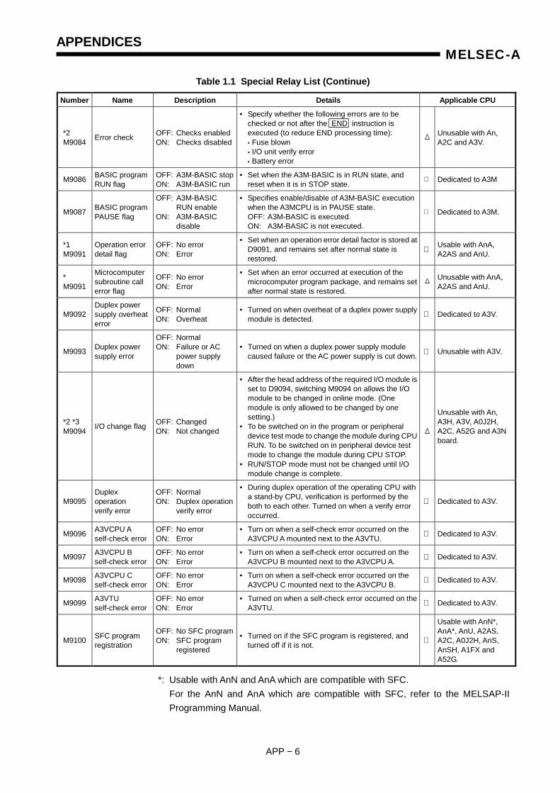
APPENDICES
APP − 6
MELSEC-A
Table 1.1 Special Relay List (Continue)
Number Name Description Details Applicable CPU
*2 M9084 Error check OFF: Checks enabled
ON: Checks disabled
• Specify whether the following errors are to be checked or not after the END instruction is executed (to reduce END processing time): • Fuse blown • I/O unit verify error • Battery error
Unusable with An, A2C and A3V.
M9086 BASIC program RUN flag
OFF: A3M-BASIC stopON: A3M-BASIC run
• Set when the A3M-BASIC is in RUN state, and reset when it is in STOP state.
Dedicated to A3M
M9087 BASIC program PAUSE flag
OFF: A3M-BASIC RUN enable ON: A3M-BASIC disable
• Specifies enable/disable of A3M-BASIC execution when the A3MCPU is in PAUSE state. OFF: A3M-BASIC is executed. ON: A3M-BASIC is not executed.
Dedicated to A3M.
*1 M9091
Operation error detail flag
OFF: No error ON: Error
• Set when an operation error detail factor is stored at D9091, and remains set after normal state is restored.
Usable with AnA, A2AS and AnU.
* M9091
Microcomputer subroutine call error flag
OFF: No error ON: Error
• Set when an error occurred at execution of the microcomputer program package, and remains set after normal state is restored.
Unusable with AnA, A2AS and AnU.
M9092 Duplex power supply overheat error
OFF: Normal ON: Overheat
• Turned on when overheat of a duplex power supply module is detected. Dedicated to A3V.
M9093 Duplex power supply error
OFF: Normal ON: Failure or AC power supply down
• Turned on when a duplex power supply module caused failure or the AC power supply is cut down. Unusable with A3V.
*2 *3 M9094 I/O change flag OFF: Changed
ON: Not changed
• After the head address of the required I/O module is set to D9094, switching M9094 on allows the I/O module to be changed in online mode. (One module is only allowed to be changed by one setting.)
• To be switched on in the program or peripheral device test mode to change the module during CPU RUN. To be switched on in peripheral device test mode to change the module during CPU STOP.
• RUN/STOP mode must not be changed until I/O module change is complete.
Unusable with An, A3H, A3V, A0J2H, A2C, A52G and A3N board.
M9095 Duplex operation verify error
OFF: Normal ON: Duplex operation verify error
• During duplex operation of the operating CPU with a stand-by CPU, verification is performed by the both to each other. Turned on when a verify error occurred.
Dedicated to A3V.
M9096 A3VCPU A self-check error
OFF: No error ON: Error
• Turn on when a self-check error occurred on the A3VCPU A mounted next to the A3VTU. Dedicated to A3V.
M9097 A3VCPU B self-check error
OFF: No error ON: Error
• Turn on when a self-check error occurred on the A3VCPU B mounted next to the A3VCPU A. Dedicated to A3V.
M9098 A3VCPU C self-check error
OFF: No error ON: Error
• Turn on when a self-check error occurred on the A3VCPU C mounted next to the A3VCPU B. Dedicated to A3V.
M9099 A3VTU self-check error
OFF: No error ON: Error
• Turned on when a self-check error occurred on the A3VTU. Dedicated to A3V.
M9100 SFC program registration
OFF: No SFC programON: SFC program registered
• Turned on if the SFC program is registered, and turned off if it is not.
Usable with AnN*, AnA*, AnU, A2AS, A2C, A0J2H, AnS, AnSH, A1FX and A52G.
*: Usable with AnN and AnA which are compatible with SFC. For the AnN and AnA which are compatible with SFC, refer to the MELSAP-II Programming Manual.

APPENDICES
APP − 7
MELSEC-A
Table 1.1 Special Relay List (Continue)
Number Name Description Details Applicable CPU
*2 M9101
SFC program start/stop
OFF: SFC program stop ON: SFC program start
• Should be turned on by the program if the SFC program is to be started. If turned off, operation output of the execution step is turned off and the SFC program is stopped.
Usable with AnN*, AnA*, AnU, A2AS, A2C, A0J2H, AnS, AnSH, A1FX and A52G.
*2 M9102
SFC program starting status
OFF: Initial start ON: Continuous start
• Selects the starting step when the SFC program is restarted using M9101.
ON: All execution conditions when the SFC program stopped are cleared, and the program is started with the initial step of block 0. OFF: Started with the step of the block being executed when the program stopped. • Once turned on, the program is latched in the
system and remains on even if the power is turned off. Should be turned off by the sequence program when turning on the power, or when starting with the initial step of block 0.
Usable with AnN*, AnA*, AnU, A2AS, A2C, A0J2H, AnS, AnSH, A1FX and A52G.
*2 M9103
Consecutive step transfer enable/disable
OFF: Consecutive step transfer disable ON: Consecutive step transfer enable
• Selects consecutive or step-by-step transfer of steps of which transfer conditions are established when all of the transfer conditions of consecutive steps are established.
ON: Consecutive transfer is executed. OFF: One step per one scan is transferred.
Usable with AnN*, AnA*, AnU, A2AS, A2C, A0J2H, AnS, AnSH, A1FX and A52G.
M9104 Consecutive transfer prevention flag
OFF: Transfer complete ON: Transfer incomplete
• Set when consecutive transfer is not executed with consecutive transfer enabled. Reset when transfer of one step is completed. Consecutive transfer of a step can be prevented by writing an AND condition to corresponding M9104.
Usable with AnN*, AnA*, AnU, A2AS, A2C, A0J2H, AnS, AnSH, A1FX and A52G.
*2 M9108
Step transfer monitoring timer start (corresponds to D9108)
*2 M9109
Step transfer monitoring timer start (corresponds to D9109)
*2 M9110
Step transfer monitoring timer start (corresponds to D9110)
*2 M9111
Step transfer monitoring timer start (corresponds to D9111)
*2 M9112
Step transfer monitoring timer start (corresponds to D9112)
OFF: Monitoring timer eset ON: Monitoring timer eset start
• Turned on when the step transfer monitoring timer is started. Turned off when the monitoring timer is reset.
Usable with AnN*, AnA*, AnU, A2AS, A2C, A0J2H, AnS, AnSH, A1FX and A52G.
*: Usable with AnN and AnA which are compatible with SFC. For the AnN and AnA which are compatible with SFC, refer to the MELSAP-II Programming Manual.
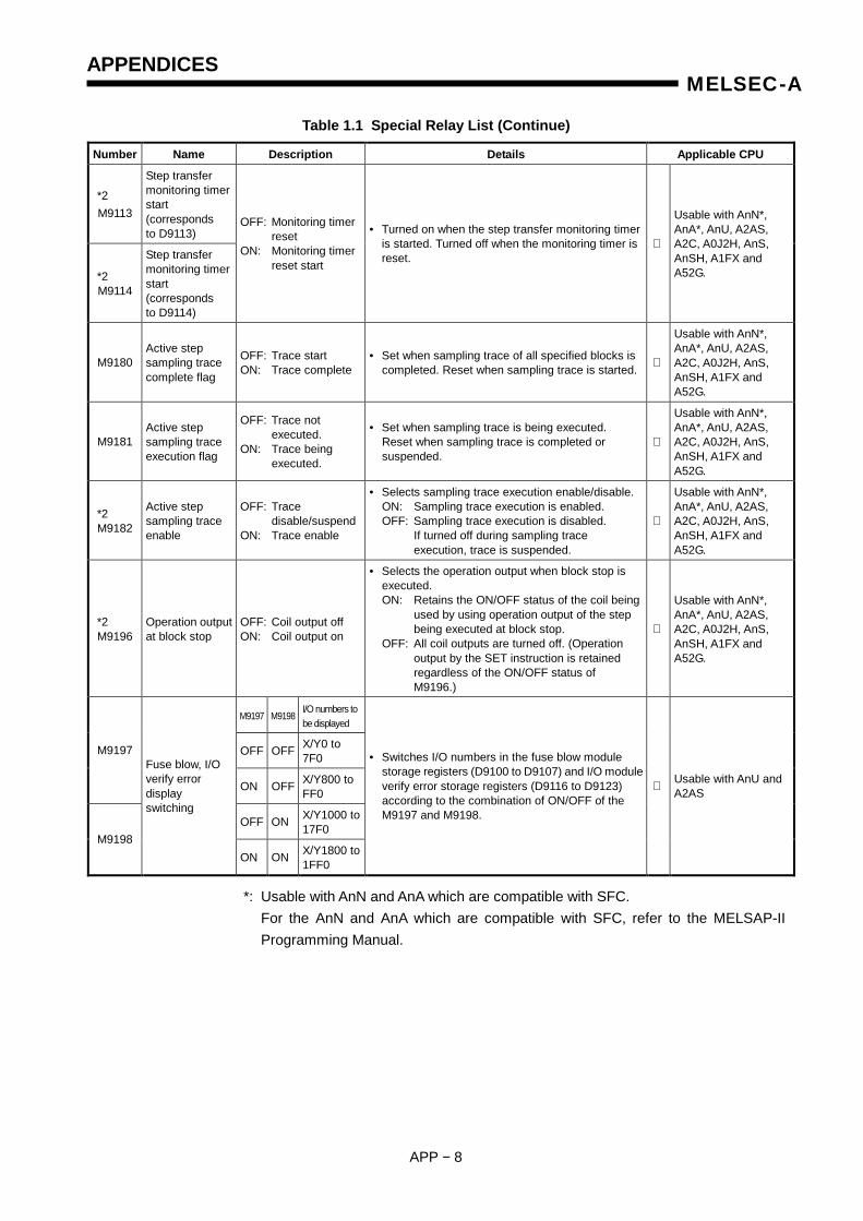
APPENDICES
APP − 8
MELSEC-A
Table 1.1 Special Relay List (Continue)
Number Name Description Details Applicable CPU
*2 M9113
Step transfer monitoring timer start (corresponds to D9113)
*2 M9114
Step transfer monitoring timer start (corresponds to D9114)
OFF: Monitoring timer reset ON: Monitoring timer reset start
• Turned on when the step transfer monitoring timer is started. Turned off when the monitoring timer is reset.
Usable with AnN*, AnA*, AnU, A2AS, A2C, A0J2H, AnS, AnSH, A1FX and A52G.
M9180 Active step sampling trace complete flag
OFF: Trace start ON: Trace complete
• Set when sampling trace of all specified blocks is completed. Reset when sampling trace is started.
Usable with AnN*, AnA*, AnU, A2AS, A2C, A0J2H, AnS, AnSH, A1FX and A52G.
M9181 Active step sampling trace execution flag
OFF: Trace not executed. ON: Trace being executed.
• Set when sampling trace is being executed. Reset when sampling trace is completed or suspended.
Usable with AnN*, AnA*, AnU, A2AS, A2C, A0J2H, AnS, AnSH, A1FX and A52G.
*2 M9182
Active step sampling trace enable
OFF: Trace disable/suspend ON: Trace enable
• Selects sampling trace execution enable/disable. ON: Sampling trace execution is enabled. OFF: Sampling trace execution is disabled. If turned off during sampling trace execution, trace is suspended.
Usable with AnN*, AnA*, AnU, A2AS, A2C, A0J2H, AnS, AnSH, A1FX and A52G.
*2 M9196
Operation output at block stop
OFF: Coil output off ON: Coil output on
• Selects the operation output when block stop is executed. ON: Retains the ON/OFF status of the coil being used by using operation output of the step being executed at block stop. OFF: All coil outputs are turned off. (Operation output by the SET instruction is retained regardless of the ON/OFF status of M9196.)
Usable with AnN*, AnA*, AnU, A2AS, A2C, A0J2H, AnS, AnSH, A1FX and A52G.
M9197 M9198 I/O numbers to be displayed
OFF OFF X/Y0 to 7F0
M9197
ON OFF X/Y800 to FF0
OFF ON X/Y1000 to 17F0
M9198
Fuse blow, I/O verify error display switching
ON ON X/Y1800 to 1FF0
• Switches I/O numbers in the fuse blow module storage registers (D9100 to D9107) and I/O module verify error storage registers (D9116 to D9123) according to the combination of ON/OFF of the M9197 and M9198.
Usable with AnU and A2AS
*: Usable with AnN and AnA which are compatible with SFC. For the AnN and AnA which are compatible with SFC, refer to the MELSAP-II Programming Manual.
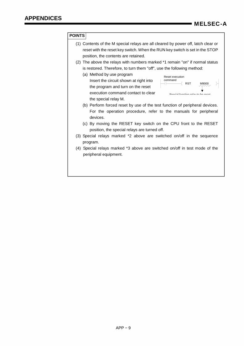
APPENDICES
APP − 9
MELSEC-A
POINTS
(1) Contents of the M special relays are all cleared by power off, latch clear or reset with the reset key switch. When the RUN key switch is set in the STOP position, the contents are retained.
(2) The above the relays with numbers marked *1 remain "on" if normal status is restored. Therefore, to turn them "off", use the following method: (a) Method by use program Insert the circuit shown at right into the program and turn on the reset execution command contact to clear the special relay M. (b) Perform forced reset by use of the test function of peripheral devices. For the operation procedure, refer to the manuals for peripheral devices. (c) By moving the RESET key switch on the CPU front to the RESET position, the special relays are turned off.
(3) Special relays marked *2 above are switched on/off in the sequence program.
(4) Special relays marked *3 above are switched on/off in test mode of the peripheral equipment.
RST M9000
Reset execution command
Special function relay to be reset
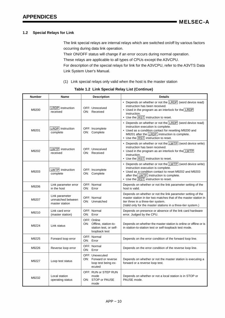
APPENDICES
APP − 10
MELSEC-A
1.2 Special Relays for Link
The link special relays are internal relays which are switched on/off by various factors occurring during data link operation. Their ON/OFF status will change if an error occurs during normal operation. These relays are applicable to all types of CPUs except the A3VCPU. For description of the special relays for link for the A3VCPU, refer to the A3VTS Data Link System User's Manual.
(1) Link special relays only valid when the host is the master station
Table 1.2 Link Special Relay List (Continue)
Number Name Description Details
M9200 LRDP instruction received
OFF: Unreceived ON: Received
• Depends on whether or not the LRDP (word device read) instruction has been received. • Used in the program as an interlock for the LRDP instruction. • Use the RST instruction to reset.
M9201 LRDP instruction complete
OFF: Incomplete ON: Complete
• Depends on whether or not the LRDP (word device read) instruction execution is complete. • Used as a condition contact for resetting M9200 and M9201 after the LRDP instruction is complete. • Use the RST instruction to reset.
M9202 LWTP instruction received
OFF: Unreceived ON: Received
• Depends on whether or not the LWTP (word device write) instruction has been received. • Used in the program as an interlock for the LWTP instruction. • Use the RST instruction to reset.
M9203 LWTP instruction complete
OFF: Incomplete ON: Complete
• Depends on whether or not the LWTP (word device write) instruction execution is complete. • Used as a condition contact to reset M9202 and M9203 after the LWTP instruction is complete. • Use the RST instruction to reset.
M9206 Link parameter error in the host
OFF: Normal ON: Error
Depends on whether or not the link parameter setting of the host is valid.
M9207 Link parameter unmatched between master station
OFF: Normal ON: Unmatched
Depends on whether or not the link parameter setting of the master station in tier two matches that of the master station in tier three in a three-tier system. (Valid only for the master stations in a three-tier system.)
M9210 Link card error (master station)
OFF: Normal ON: Error
Depends on presence or absence of the link card hardware error. Judged by the CPU.
M9224 Link status
OFF: Online ON: Offline, station-to- station test, or self- loopback test
Depends on whether the master station is online or offline or is in station-to-station test or self-loopback test mode.
M9225 Forward loop error OFF: Normal ON: Error Depends on the error condition of the forward loop line.
M9226 Reverse loop error OFF: Normal ON: Error Depends on the error condition of the reverse loop line.
M9227 Loop test status
OFF: Unexecuted ON: Forward or reverse loop test being ex- ecuted
Depends on whether or not the master station is executing a forward or a reverse loop test.
M9232 Local station operating status
OFF: RUN or STEP RUN mode ON: STOP or PAUSE mode
Depends on whether or not a local station is in STOP or PAUSE mode.
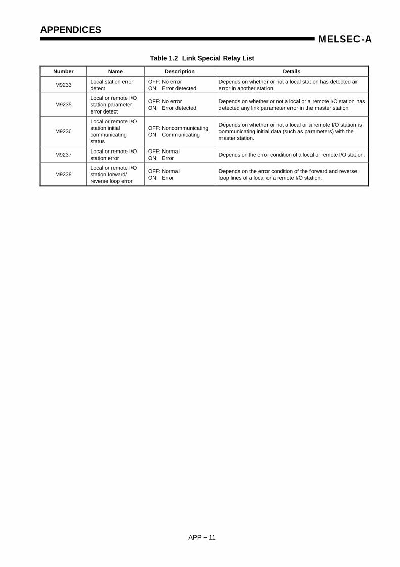
APPENDICES
APP − 11
MELSEC-A
Table 1.2 Link Special Relay List
Number Name Description Details
M9233 Local station error detect
OFF: No error ON: Error detected
Depends on whether or not a local station has detected an error in another station.
M9235 Local or remote I/O station parameter error detect
OFF: No error ON: Error detected
Depends on whether or not a local or a remote I/O station has detected any link parameter error in the master station
M9236
Local or remote I/O station initial communicating status
OFF: Noncommunicating ON: Communicating
Depends on whether or not a local or a remote I/O station is communicating initial data (such as parameters) with the master station.
M9237 Local or remote I/O station error
OFF: Normal ON: Error Depends on the error condition of a local or remote I/O station.
M9238 Local or remote I/O station forward/ reverse loop error
OFF: Normal ON: Error
Depends on the error condition of the forward and reverse loop lines of a local or a remote I/O station.
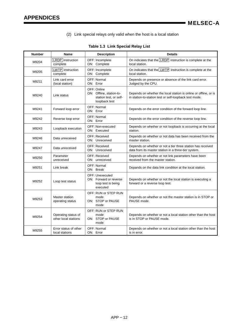
APPENDICES
APP − 12
MELSEC-A
(2) Link special relays only valid when the host is a local station
Table 1.3 Link Special Relay List
Number Name Description Details
M9204 LRDP instruction complete
OFF: Incomplete ON: Complete
On indicates that the LRDP instruction is complete at the local station.
M9205 LWTP instruction complete
OFF: Incomplete ON: Complete
On indicates that the LWTP instruction is complete at the local station.
M9211 Link card error (local station)
OFF: Normal ON: Error
Depends on presence or absence of the link card error. Judged by the CPU.
M9240 Link status
OFF: Online ON: Offline, station-to- station test, or self- loopback test
Depends on whether the local station is online or offline, or is in station-to-station test or self-loopback test mode.
M9241 Forward loop error OFF: Normal ON: Error Depends on the error condition of the forward loop line.
M9242 Reverse loop error OFF: Normal ON: Error Depends on the error condition of the reverse loop line.
M9243 Loopback execution OFF: Non-executed ON: Executed
Depends on whether or not loopback is occurring at the local station.
M9246 Data unreceived OFF: Received ON: Unreceived
Depends on whether or not data has been received from the master station.
M9247 Data unreceived OFF: Received ON: Unreceived
Depends on whether or not a tier three station has received data from its master station in a three-tier system.
M9250 Parameter unreceived
OFF: Received ON: unreceived
Depends on whether or not link parameters have been received from the master station.
M9251 Link break OFF: Normal ON: Break Depands on the data link condition at the local station.
M9252 Loop test status
OFF: Unexecuted ON: Forward or reverse loop test is being executed
Depends on whether or not the local station is executing a forward or a reverse loop test.
M9253 Master station operating status
OFF: RUN or STEP RUN mode ON: STOP or PAUSE mode
Depends on whether or not the master station is in STOP or PAUSE mode.
M9254 Operating status of other local stations
OFF: RUN or STEP RUN mode ON: STOP or PAUSE mode
Depends on whether or not a local station other than the host is in STOP or PAUSE mode.
M9255 Error status of other local stations
OFF: Normal ON: Error
Depends on whether or not a local station other than the host is in error.
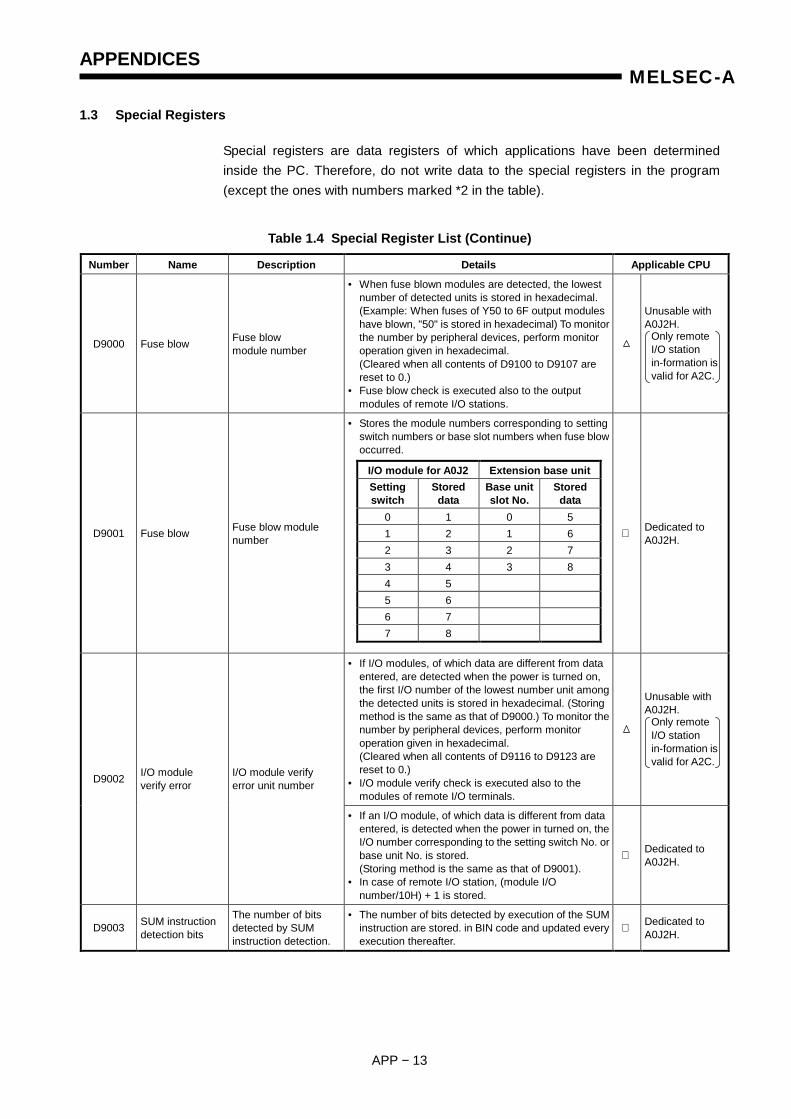
APPENDICES
APP − 13
MELSEC-A
1.3 Special Registers
Special registers are data registers of which applications have been determined inside the PC. Therefore, do not write data to the special registers in the program (except the ones with numbers marked *2 in the table).
Table 1.4 Special Register List (Continue)
Number Name Description Details Applicable CPU
D9000 Fuse blow Fuse blow module number
• When fuse blown modules are detected, the lowest number of detected units is stored in hexadecimal. (Example: When fuses of Y50 to 6F output modules have blown, "50" is stored in hexadecimal) To monitor the number by peripheral devices, perform monitor operation given in hexadecimal. (Cleared when all contents of D9100 to D9107 are reset to 0.)
• Fuse blow check is executed also to the output modules of remote I/O stations.
Unusable with A0J2H.
D9001 Fuse blow Fuse blow module number
• Stores the module numbers corresponding to setting switch numbers or base slot numbers when fuse blow occurred.
Dedicated to A0J2H.
• If I/O modules, of which data are different from data entered, are detected when the power is turned on, the first I/O number of the lowest number unit among the detected units is stored in hexadecimal. (Storing method is the same as that of D9000.) To monitor the number by peripheral devices, perform monitor operation given in hexadecimal. (Cleared when all contents of D9116 to D9123 are reset to 0.)
• I/O module verify check is executed also to the modules of remote I/O terminals.
Unusable with A0J2H.
D9002 I/O module verify error
I/O module verify error unit number
• If an I/O module, of which data is different from data entered, is detected when the power in turned on, the I/O number corresponding to the setting switch No. or base unit No. is stored. (Storing method is the same as that of D9001).
• In case of remote I/O station, (module I/O number/10H) + 1 is stored.
Dedicated to A0J2H.
D9003 SUM instruction detection bits
The number of bits detected by SUM instruction detection.
• The number of bits detected by execution of the SUM instruction are stored. in BIN code and updated every execution thereafter.
Dedicated to A0J2H.
I/O module for A0J2 Extension base unit Setting switch
Stored data
Base unit slot No.
Stored data
0 1 0 5 1 2 1 6 2 3 2 7 3 4 3 8 4 5 5 6 6 7 7 8
Only remote I/O station in-formation isvalid for A2C.
Only remote I/O station in-formation isvalid for A2C.
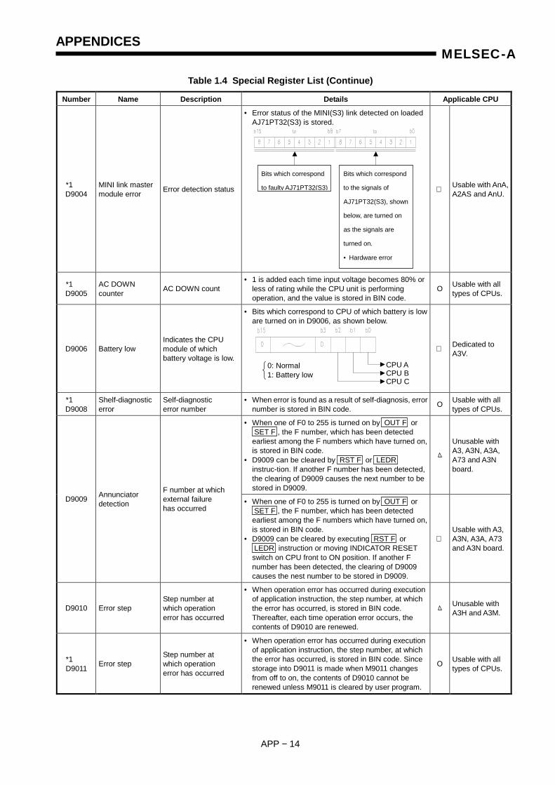
APPENDICES
APP − 14
MELSEC-A
Table 1.4 Special Register List (Continue)
Number Name Description Details Applicable CPU
*1 D9004
MINI link master module error Error detection status
• Error status of the MINI(S3) link detected on loaded AJ71PT32(S3) is stored.
Usable with AnA, A2AS and AnU.
*1 D9005
AC DOWN counter AC DOWN count
• 1 is added each time input voltage becomes 80% or less of rating while the CPU unit is performing operation, and the value is stored in BIN code.
O Usable with all types of CPUs.
D9006 Battery low Indicates the CPU module of which battery voltage is low.
• Bits which correspond to CPU of which battery is low are turned on in D9006, as shown below.
Dedicated to A3V.
*1 D9008
Shelf-diagnostic error
Self-diagnostic error number
• When error is found as a result of self-diagnosis, error number is stored in BIN code. O Usable with all
types of CPUs.
• When one of F0 to 255 is turned on by OUT F or SET F , the F number, which has been detected earliest among the F numbers which have turned on, is stored in BIN code.
• D9009 can be cleared by RST F or LEDR instruc-tion. If another F number has been detected, the clearing of D9009 causes the next number to be stored in D9009.
Unusable with A3, A3N, A3A, A73 and A3N board.
D9009 Annunciator detection
F number at which external failure has occurred
• When one of F0 to 255 is turned on by OUT F or SET F , the F number, which has been detected earliest among the F numbers which have turned on, is stored in BIN code.
• D9009 can be cleared by executing RST F or LEDR instruction or moving INDICATOR RESET switch on CPU front to ON position. If another F number has been detected, the clearing of D9009 causes the nest number to be stored in D9009.
Usable with A3, A3N, A3A, A73 and A3N board.
D9010 Error step Step number at which operation error has occurred
• When operation error has occurred during execution of application instruction, the step number, at which the error has occurred, is stored in BIN code. Thereafter, each time operation error occurs, the contents of D9010 are renewed.
Unusable with A3H and A3M.
*1 D9011 Error step
Step number at which operation error has occurred
• When operation error has occurred during execution of application instruction, the step number, at which the error has occurred, is stored in BIN code. Since storage into D9011 is made when M9011 changes from off to on, the contents of D9010 cannot be renewed unless M9011 is cleared by user program.
O Usable with all types of CPUs.
Bits which correspond
to the signals of
AJ71PT32(S3), shown
below, are turned on
as the signals are
turned on.
• Hardware error
Bits which correspond
to faulty AJ71PT32(S3)
CPU A CPU B CPU C
0: Normal 1: Battery low
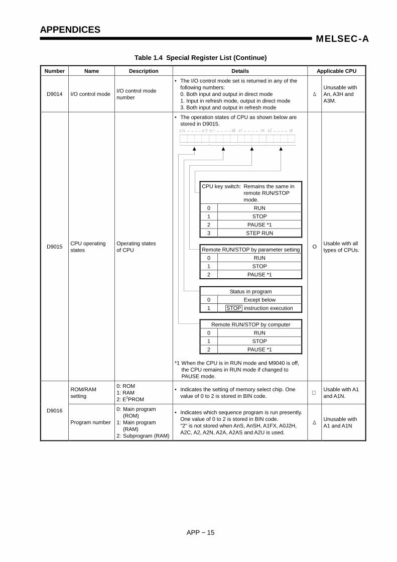
APPENDICES
APP − 15
MELSEC-A
Table 1.4 Special Register List (Continue)
Number Name Description Details Applicable CPU
D9014 I/O control mode I/O control mode number
• The I/O control mode set is returned in any of the following numbers: 0. Both input and output in direct mode 1. Input in refresh mode, output in direct mode 3. Both input and output in refresh mode
Unusable with An, A3H and A3M.
D9015 CPU operating states
Operating states of CPU
• The operation states of CPU as shown below are stored in D9015.
*1 When the CPU is in RUN mode and M9040 is off, the CPU remains in RUN mode if changed to PAUSE mode.
O Usable with all types of CPUs.
ROM/RAM setting
0: ROM 1: RAM 2: E2PROM
• Indicates the setting of memory select chip. One value of 0 to 2 is stored in BIN code. Usable with A1
and A1N.
D9016
Program number
0: Main program (ROM) 1: Main program (RAM) 2: Subprogram (RAM)
• Indicates which sequence program is run presently. One value of 0 to 2 is stored in BIN code. "2" is not stored when AnS, AnSH, A1FX, A0J2H, A2C, A2, A2N, A2A, A2AS and A2U is used.
Unusable with A1 and A1N
CPU key switch: Remains the same in remote RUN/STOP mode.
0 RUN 1 STOP 2 PAUSE *1 3 STEP RUN
Remote RUN/STOP by parameter setting 0 RUN 1 STOP 2 PAUSE *1
Status in program 0 Except below 1 STOP instruction execution
Remote RUN/STOP by computer 0 RUN 1 STOP 2 PAUSE *1
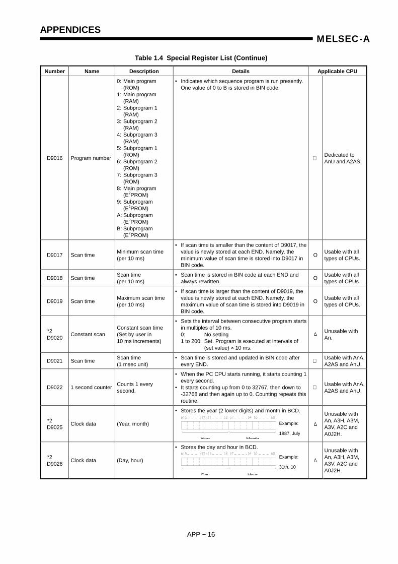
APPENDICES
APP − 16
MELSEC-A
Table 1.4 Special Register List (Continue)
Number Name Description Details Applicable CPU
D9016 Program number
0: Main program (ROM) 1: Main program (RAM) 2: Subprogram 1 (RAM) 3: Subprogram 2 (RAM) 4: Subprogram 3 (RAM) 5: Subprogram 1 (ROM) 6: Subprogram 2 (ROM) 7: Subprogram 3 (ROM) 8: Main program (E2PROM) 9: Subprogram (E2PROM) A: Subprogram (E2PROM) B: Subprogram (E2PROM)
• Indicates which sequence program is run presently. One value of 0 to B is stored in BIN code.
Dedicated to AnU and A2AS.
D9017 Scan time Minimum scan time (per 10 ms)
• If scan time is smaller than the content of D9017, the value is newly stored at each END. Namely, the minimum value of scan time is stored into D9017 in BIN code.
O Usable with all types of CPUs.
D9018 Scan time Scan time (per 10 ms)
• Scan time is stored in BIN code at each END and always rewritten. O Usable with all
types of CPUs.
D9019 Scan time Maximum scan time (per 10 ms)
• If scan time is larger than the content of D9019, the value is newly stored at each END. Namely, the maximum value of scan time is stored into D9019 in BIN code.
O Usable with all types of CPUs.
*2 D9020 Constant scan
Constant scan time (Set by user in 10 ms increments)
• Sets the interval between consecutive program starts in multiples of 10 ms. 0: No setting 1 to 200: Set. Program is executed at intervals of (set value) × 10 ms.
Unusable with An.
D9021 Scan time Scan time (1 msec unit)
• Scan time is stored and updated in BIN code after every END. Usable with AnA,
A2AS and AnU.
D9022 1 second counter Counts 1 every second.
• When the PC CPU starts running, it starts counting 1 every second.
• It starts counting up from 0 to 32767, then down to -32768 and then again up to 0. Counting repeats this routine.
Usable with AnA, A2AS and AnU.
*2 D9025 Clock data (Year, month)
• Stores the year (2 lower digits) and month in BCD.
Unusable with An, A3H, A3M, A3V, A2C and A0J2H.
*2 D9026 Clock data (Day, hour)
• Stores the day and hour in BCD.
Unusable with An, A3H, A3M, A3V, A2C and A0J2H.
Example:
1987, July Year Month
Example:
31th, 10
’ l kDay Hour
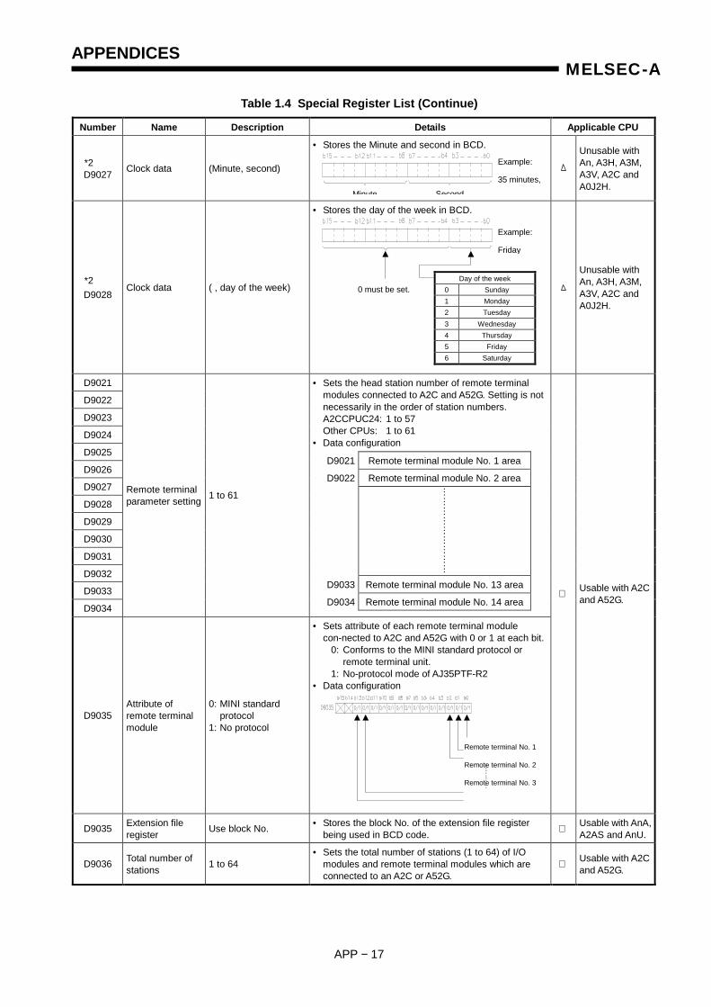
APPENDICES
APP − 17
MELSEC-A
Table 1.4 Special Register List (Continue)
Number Name Description Details Applicable CPU
*2 D9027 Clock data (Minute, second)
• Stores the Minute and second in BCD.
Unusable with An, A3H, A3M, A3V, A2C and A0J2H.
*2 D9028
Clock data ( , day of the week)
• Stores the day of the week in BCD.
Unusable with An, A3H, A3M, A3V, A2C and A0J2H.
D9021
D9022
D9023
D9024
D9025
D9026
D9027
D9028
D9029
D9030
D9031
D9032
D9033
D9034
Remote terminal parameter setting 1 to 61
• Sets the head station number of remote terminal modules connected to A2C and A52G. Setting is not necessarily in the order of station numbers. A2CCPUC24: 1 to 57 Other CPUs: 1 to 61
• Data configuration
D9035 Attribute of remote terminal module
0: MINI standard protocol 1: No protocol
• Sets attribute of each remote terminal module con-nected to A2C and A52G with 0 or 1 at each bit. 0: Conforms to the MINI standard protocol or remote terminal unit. 1: No-protocol mode of AJ35PTF-R2
• Data configuration
Usable with A2C and A52G.
D9035 Extension file register Use block No. • Stores the block No. of the extension file register
being used in BCD code. Usable with AnA, A2AS and AnU.
D9036 Total number of stations 1 to 64
• Sets the total number of stations (1 to 64) of I/O modules and remote terminal modules which are connected to an A2C or A52G.
Usable with A2C and A52G.
Example:
35 minutes,
Minute Second
Example:
Friday
Day of the week 0 Sunday 1 Monday 2 Tuesday 3 Wednesday 4 Thursday 5 Friday 6 Saturday
0 must be set.
D9021 Remote terminal module No. 1 area
D9022 Remote terminal module No. 2 area
D9033 Remote terminal module No. 13 area
D9034 Remote terminal module No. 14 area
……
……
……
……
…
Remote terminal No. 1
Remote terminal No. 2
Remote terminal No. 3
……
…..
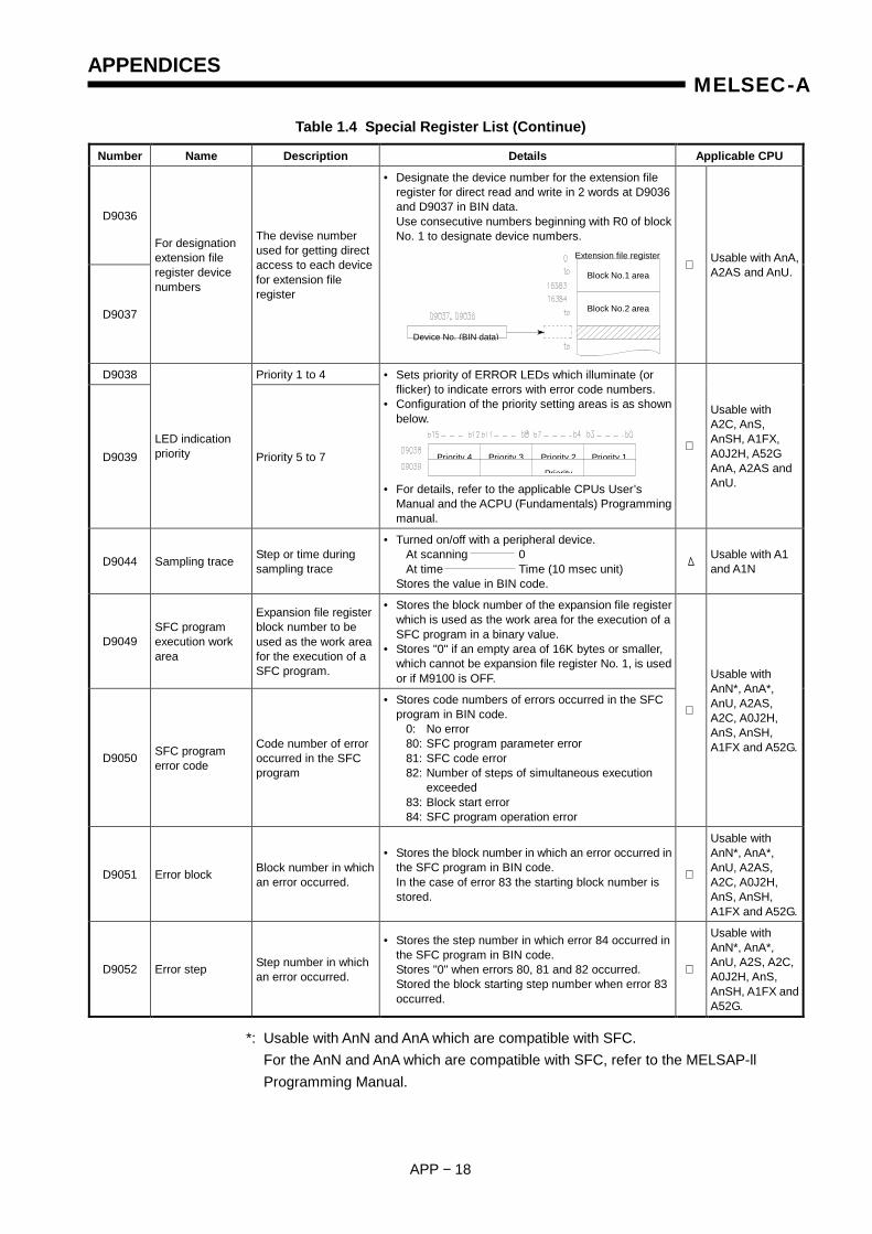
APPENDICES
APP − 18
MELSEC-A
Table 1.4 Special Register List (Continue)
Number Name Description Details Applicable CPU
D9036
D9037
For designation extension file register device numbers
The devise number used for getting direct access to each device for extension file register
• Designate the device number for the extension file register for direct read and write in 2 words at D9036 and D9037 in BIN data. Use consecutive numbers beginning with R0 of block No. 1 to designate device numbers.
Usable with AnA, A2AS and AnU.
D9038 Priority 1 to 4
D9039 LED indication priority Priority 5 to 7
• Sets priority of ERROR LEDs which illuminate (or flicker) to indicate errors with error code numbers.
• Configuration of the priority setting areas is as shown below.
• For details, refer to the applicable CPUs User’s
Manual and the ACPU (Fundamentals) Programming manual.
Usable with A2C, AnS, AnSH, A1FX, A0J2H, A52G AnA, A2AS and AnU.
D9044 Sampling trace Step or time during sampling trace
• Turned on/off with a peripheral device. At scanning 0 At time Time (10 msec unit) Stores the value in BIN code.
Usable with A1 and A1N
D9049 SFC program execution work area
Expansion file register block number to be used as the work area for the execution of a SFC program.
• Stores the block number of the expansion file register which is used as the work area for the execution of a SFC program in a binary value.
• Stores "0" if an empty area of 16K bytes or smaller, which cannot be expansion file register No. 1, is used or if M9100 is OFF.
D9050 SFC program error code
Code number of error occurred in the SFC program
• Stores code numbers of errors occurred in the SFC program in BIN code. 0: No error 80: SFC program parameter error 81: SFC code error 82: Number of steps of simultaneous execution exceeded 83: Block start error 84: SFC program operation error
Usable with AnN*, AnA*, AnU, A2AS, A2C, A0J2H, AnS, AnSH, A1FX and A52G.
D9051 Error block Block number in which an error occurred.
• Stores the block number in which an error occurred in the SFC program in BIN code. In the case of error 83 the starting block number is stored.
Usable with AnN*, AnA*, AnU, A2AS, A2C, A0J2H, AnS, AnSH, A1FX and A52G.
D9052 Error step Step number in which an error occurred.
• Stores the step number in which error 84 occurred in the SFC program in BIN code. Stores "0" when errors 80, 81 and 82 occurred. Stored the block starting step number when error 83 occurred.
Usable with AnN*, AnA*, AnU, A2S, A2C, A0J2H, AnS, AnSH, A1FX and A52G.
*: Usable with AnN and AnA which are compatible with SFC. For the AnN and AnA which are compatible with SFC, refer to the MELSAP-ll Programming Manual.
Extension file register
Device No. (BIN data)
Block No.1 area
Block No.2 area
Priority 4 Priority 3 Priority 2 Priority 1
Priority
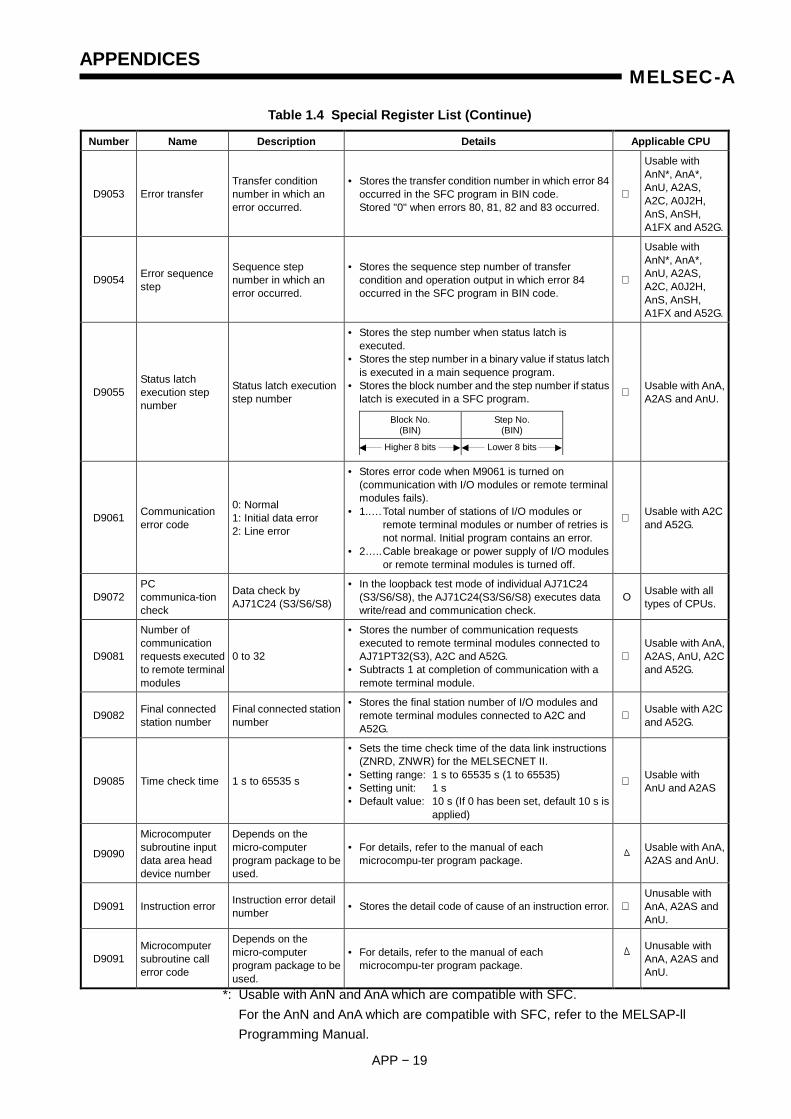
APPENDICES
APP − 19
MELSEC-A
Table 1.4 Special Register List (Continue)
Number Name Description Details Applicable CPU
D9053 Error transfer Transfer condition number in which an error occurred.
• Stores the transfer condition number in which error 84 occurred in the SFC program in BIN code. Stored "0" when errors 80, 81, 82 and 83 occurred.
Usable with AnN*, AnA*, AnU, A2AS, A2C, A0J2H, AnS, AnSH, A1FX and A52G.
D9054 Error sequence step
Sequence step number in which an error occurred.
• Stores the sequence step number of transfer condition and operation output in which error 84 occurred in the SFC program in BIN code.
Usable with AnN*, AnA*, AnU, A2AS, A2C, A0J2H, AnS, AnSH, A1FX and A52G.
D9055 Status latch execution step number
Status latch execution step number
• Stores the step number when status latch is executed.
• Stores the step number in a binary value if status latch is executed in a main sequence program.
• Stores the block number and the step number if status latch is executed in a SFC program.
Usable with AnA, A2AS and AnU.
D9061 Communication error code
0: Normal 1: Initial data error 2: Line error
• Stores error code when M9061 is turned on (communication with I/O modules or remote terminal modules fails).
• 1..… Total number of stations of I/O modules or remote terminal modules or number of retries is not normal. Initial program contains an error.
• 2….. Cable breakage or power supply of I/O modules or remote terminal modules is turned off.
Usable with A2C and A52G.
D9072 PC communica-tion check
Data check by AJ71C24 (S3/S6/S8)
• In the loopback test mode of individual AJ71C24 (S3/S6/S8), the AJ71C24(S3/S6/S8) executes data write/read and communication check.
O Usable with all types of CPUs.
D9081
Number of communication requests executed to remote terminal modules
0 to 32
• Stores the number of communication requests executed to remote terminal modules connected to AJ71PT32(S3), A2C and A52G.
• Subtracts 1 at completion of communication with a remote terminal module.
Usable with AnA, A2AS, AnU, A2C and A52G.
D9082 Final connected station number
Final connected station number
• Stores the final station number of I/O modules and remote terminal modules connected to A2C and A52G.
Usable with A2C and A52G.
D9085 Time check time 1 s to 65535 s
• Sets the time check time of the data link instructions (ZNRD, ZNWR) for the MELSECNET II.
• Setting range: 1 s to 65535 s (1 to 65535) • Setting unit: 1 s • Default value: 10 s (If 0 has been set, default 10 s is
applied)
Usable with AnU and A2AS
D9090
Microcomputer subroutine input data area head device number
Depends on the micro-computer program package to be used.
• For details, refer to the manual of each microcompu-ter program package. Usable with AnA,
A2AS and AnU.
D9091 Instruction error Instruction error detail number • Stores the detail code of cause of an instruction error.
Unusable with AnA, A2AS and AnU.
D9091 Microcomputer subroutine call error code
Depends on the micro-computer program package to be used.
• For details, refer to the manual of each microcompu-ter program package.
Unusable with AnA, A2AS and AnU.
Block No. (BIN)
Step No. (BIN)
Higher 8 bits Lower 8 bits
*: Usable with AnN and AnA which are compatible with SFC. For the AnN and AnA which are compatible with SFC, refer to the MELSAP-ll Programming Manual.
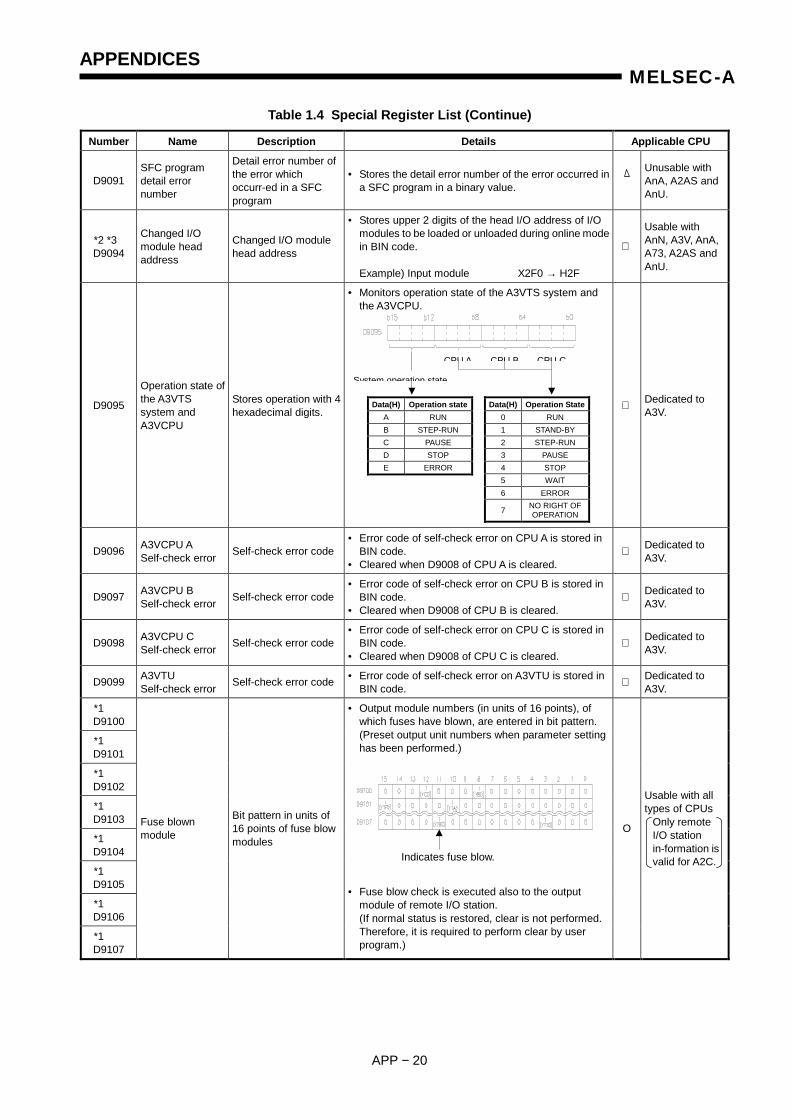
APPENDICES
APP − 20
MELSEC-A
Table 1.4 Special Register List (Continue)
Number Name Description Details Applicable CPU
D9091 SFC program detail error number
Detail error number of the error which occurr-ed in a SFC program
• Stores the detail error number of the error occurred in a SFC program in a binary value.
Unusable with AnA, A2AS and AnU.
*2 *3 D9094
Changed I/O module head address
Changed I/O module head address
• Stores upper 2 digits of the head I/O address of I/O modules to be loaded or unloaded during online mode in BIN code. Example) Input module X2F0 → H2F
Usable with AnN, A3V, AnA, A73, A2AS and AnU.
D9095
Operation state of the A3VTS system and A3VCPU
Stores operation with 4 hexadecimal digits.
• Monitors operation state of the A3VTS system and the A3VCPU.
Dedicated to A3V.
D9096 A3VCPU A Self-check error Self-check error code
• Error code of self-check error on CPU A is stored in BIN code.
• Cleared when D9008 of CPU A is cleared. Dedicated to
A3V.
D9097 A3VCPU B Self-check error Self-check error code
• Error code of self-check error on CPU B is stored in BIN code.
• Cleared when D9008 of CPU B is cleared. Dedicated to
A3V.
D9098 A3VCPU C Self-check error Self-check error code
• Error code of self-check error on CPU C is stored in BIN code.
• Cleared when D9008 of CPU C is cleared. Dedicated to
A3V.
D9099 A3VTU Self-check error Self-check error code • Error code of self-check error on A3VTU is stored in
BIN code. Dedicated to A3V.
*1 D9100
*1 D9101
*1 D9102
*1 D9103
*1 D9104
*1 D9105
*1 D9106
*1 D9107
Fuse blown module
Bit pattern in units of 16 points of fuse blow modules
• Output module numbers (in units of 16 points), of which fuses have blown, are entered in bit pattern. (Preset output unit numbers when parameter setting has been performed.)
• Fuse blow check is executed also to the output module of remote I/O station. (If normal status is restored, clear is not performed. Therefore, it is required to perform clear by user program.)
O
Usable with all types of CPUs
CPU A CPU B CPU C
System operation state
Data(H) Operation stateA RUN B STEP-RUN C PAUSE D STOP E ERROR
Data(H) Operation State 0 RUN 1 STAND-BY 2 STEP-RUN 3 PAUSE 4 STOP 5 WAIT 6 ERROR
7 NO RIGHT OF OPERATION
Only remote I/O station in-formation is valid for A2C.Indicates fuse blow.
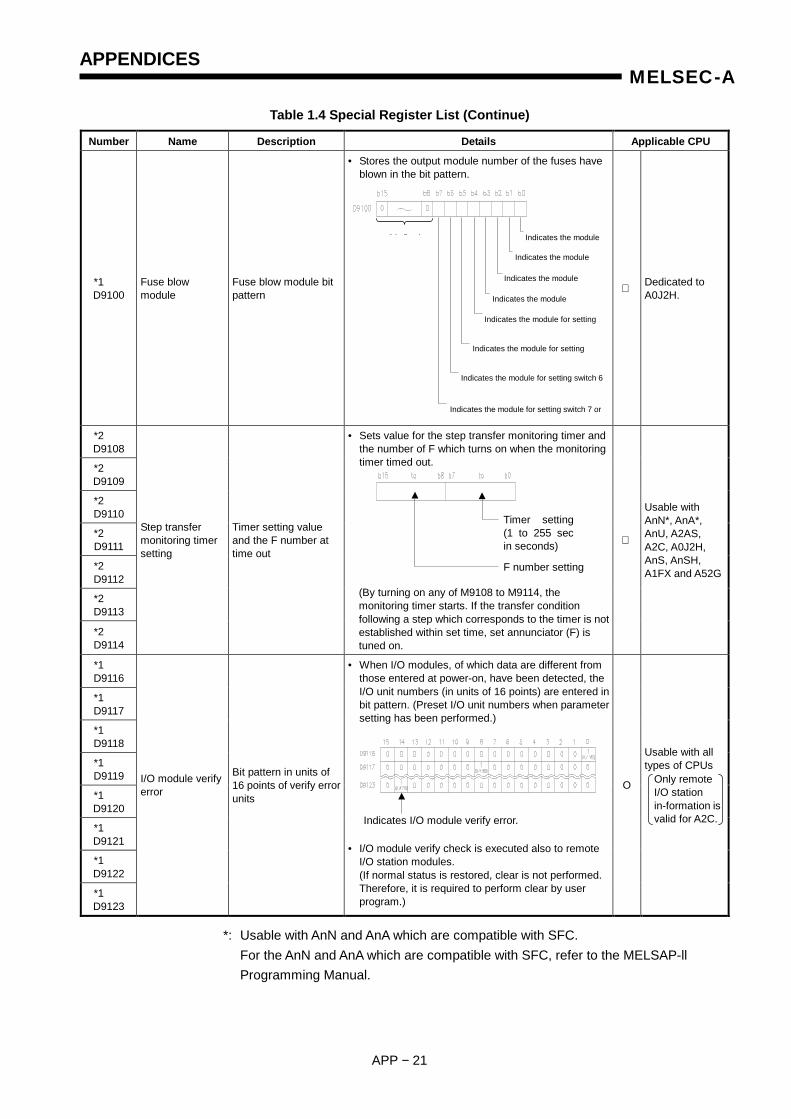
APPENDICES
APP − 21
MELSEC-A
Table 1.4 Special Register List (Continue)
Number Name Description Details Applicable CPU
*1 D9100
Fuse blow module
Fuse blow module bit pattern
• Stores the output module number of the fuses have blown in the bit pattern.
Dedicated to A0J2H.
*2 D9108
*2 D9109
*2 D9110
*2 D9111
*2 D9112
*2 D9113
*2 D9114
Step transfer monitoring timer setting
Timer setting value and the F number at time out
• Sets value for the step transfer monitoring timer and the number of F which turns on when the monitoring timer timed out.
(By turning on any of M9108 to M9114, the monitoring timer starts. If the transfer condition following a step which corresponds to the timer is not established within set time, set annunciator (F) is tuned on.
Usable with AnN*, AnA*, AnU, A2AS, A2C, A0J2H, AnS, AnSH, A1FX and A52G
*1 D9116
*1 D9117
*1 D9118
*1 D9119
*1 D9120
*1 D9121
*1 D9122
*1 D9123
I/O module verify error
Bit pattern in units of 16 points of verify error units
• When I/O modules, of which data are different from those entered at power-on, have been detected, the I/O unit numbers (in units of 16 points) are entered in bit pattern. (Preset I/O unit numbers when parameter setting has been performed.)
• I/O module verify check is executed also to remote I/O station modules. (If normal status is restored, clear is not performed. Therefore, it is required to perform clear by user program.)
O
Usable with all types of CPUs
*: Usable with AnN and AnA which are compatible with SFC. For the AnN and AnA which are compatible with SFC, refer to the MELSAP-ll Programming Manual.
Timer setting (1 to 255 sec in seconds)
F number setting
Only remote I/O station in-formation is valid for A2C.
0 i fi d Indicates the module
Indicates the module
Indicates the module
Indicates the module
Indicates the module for setting
Indicates the module for setting
Indicates the module for setting switch 6
fIndicates the module for setting switch 7 or
f
Indicates I/O module verify error.
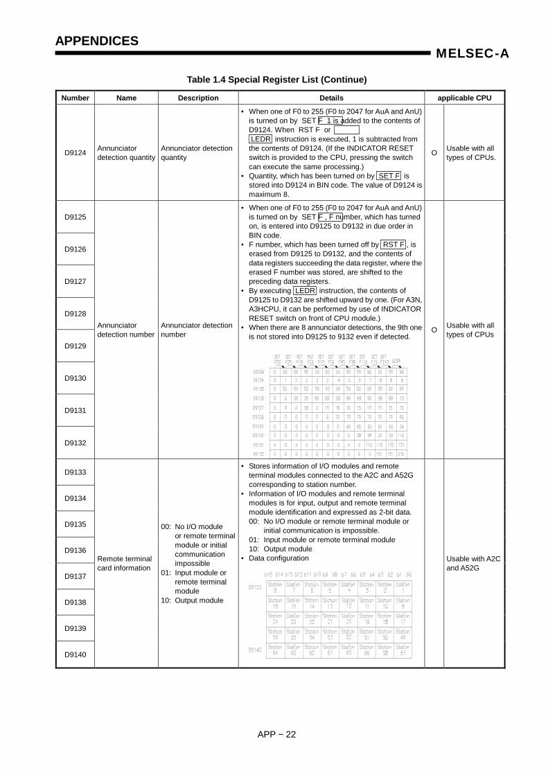
APPENDICES
APP − 22
MELSEC-A
Table 1.4 Special Register List (Continue)
Number Name Description Details applicable CPU
D9124 Annunciator detection quantity
Annunciator detection quantity
• When one of F0 to 255 (F0 to 2047 for AuA and AnU) is turned on by SET F 1 is added to the contents of D9124. When RST F or LEDR instruction is executed, 1 is subtracted from the contents of D9124. (If the INDICATOR RESET switch is provided to the CPU, pressing the switch can execute the same processing.)
• Quantity, which has been turned on by SET F is stored into D9124 in BIN code. The value of D9124 is maximum 8.
O Usable with all types of CPUs.
D9125
D9126
D9127
D9128
D9129
D9130
D9131
D9132
Annunciator detection number
Annunciator detection number
• When one of F0 to 255 (F0 to 2047 for AuA and AnU) is turned on by SET F , F number, which has turned on, is entered into D9125 to D9132 in due order in BIN code.
• F number, which has been turned off by RST F , is erased from D9125 to D9132, and the contents of data registers succeeding the data register, where the erased F number was stored, are shifted to the preceding data registers.
• By executing LEDR instruction, the contents of D9125 to D9132 are shifted upward by one. (For A3N, A3HCPU, it can be performed by use of INDICATOR RESET switch on front of CPU module.)
• When there are 8 annunciator detections, the 9th one is not stored into D9125 to 9132 even if detected.
O Usable with all types of CPUs
D9133
D9134
D9135
D9136
D9137
D9138
D9139
D9140
Remote terminal card information
00: No I/O module or remote terminal module or initial communication impossible 01: Input module or remote terminal module 10: Output module
• Stores information of I/O modules and remote terminal modules connected to the A2C and A52G corresponding to station number.
• Information of I/O modules and remote terminal modules is for input, output and remote terminal module identification and expressed as 2-bit data. 00: No I/O module or remote terminal module or initial communication is impossible. 01: Input module or remote terminal module 10: Output module
• Data configuration
Usable with A2C and A52G

APPENDICES
APP − 23
MELSEC-A
Table 1.4 Special Register List (Continue)
Number Name Description Details Applicable CPU
D9141
D9142
D9143
D9144
D9145
D9146
D9147
D9148
D9149
D9150
D9151
D9152
D9153
D9154
D9155
D9156
D9157
D9158
D9159
D9160
D9161
D9162
D9163
D9164
D9165
D9166
D9167
D9168
D9169
D9170
D9171
D9172
Number of times of retry execution Number of retries
• Stores the number of retries executed to I/O modules or remote terminal modules which caused communication error. (Retry processing is executed the number of times set at D9174.)
• Data becomes 0 when communication is restored to normal.
• Station number setting of I/O modules and remote terminal modules is as shown below.
• Retry counter uses 8 bits for one station.
* "n" is determined by station number of I/O module or remote terminal module. Odd number stations: b0 to b7 (n = 0) Even number stations: b8 to b15 (n = 8)
Usable with A2C and A52G.
Number of retries
0: Normal 1: Station error
APPENDICES
APP − 24
MELSEC-A
Table 1.4 Special Register List (Continue)
Number Name Description Details Applicable CPU
• Mode setting
0 Auto-matic online return enabled
• When an I/O module or a remote terminal module caused communica-tion error, the station is placed offline.
Communication with normal stations is continued. • When a faulty station returned to
normal, it is placed online.
1 Auto-matic online return disabled
• When an I/O module or a remote terminal module caused communica-tion error, the station is placed offline.
Communication with normal stations is continued. • Though a faulty station returned to
normal, communication is not restored unless the station module is restarted.
2 Trans-mission stop at online error
• When an I/O module or a remote terminal module caused communica-tion error, communication with all stations is stopped.
• Though a faulty station returned to normal, communication is not restored unless the station module is restarted.
D9173 Mode setting
0: Automatic online return enabled 1: Automatic online return disabled 2: Transmission stop at online error 3: Line check
3 Line check
• Checks hardware and connecting cables of I/O modules and remote terminal modules.
Usable with A2C and A52G.
D9174 Setting of the number of retries Number of retries
• Sets the number of retries executed to I/O modules and remote terminal modules which caused communication error.
• Set for 5 times at power on. • Set range: 0 to 32 • If communication with an I/O module or a remote
terminal module is not restored to normal after set number of retries, such module is regarded as a faulty station.
Usable with A2C and A52G.
D9175 Line error retry counter Number of retries
• Stores the number of retries executed at line error (time out).
• Data becomes 0 when line is restored to normal and communication with I/O modules and remote terminal modules is resumed.
Usable with A2C and A52G.
D9180 D9181 D9182 D9183 D9184 D9185 D9186 D9187 D9188 D9189 D9190 D9191 D9192 D9193
Remote terminal module error number
• Stores error code of a faulty remote terminal module when M9060 is turned on.
• The error code storage areas for each remote terminal module are as shown below.
• Error code is cleared in the following cases. When the RUN key switch is moved from STOP to RUN. (D9180 to D9183 are all cleared.) When Yn4 of each remote terminal is set from OFF to ON.
Usable with A2C and A52G.
Remote terminal module numbers from 1 to 14 are set with D9020 to D9034.
D9180 Remote terminal module No. 1D9180 Remote terminal module No. 2D9182 Remote terminal module No. 3
D9192 Remote terminal module No. 13D9193 Remote terminal module No. 14
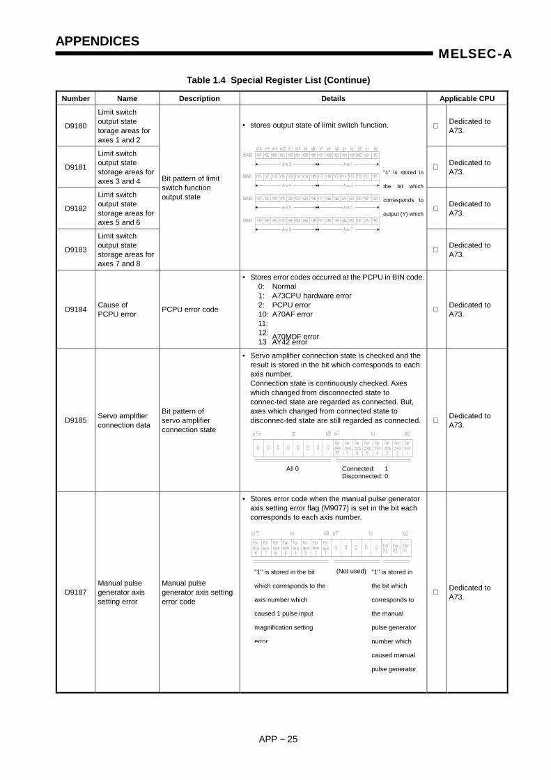
APPENDICES
APP − 25
MELSEC-A
Table 1.4 Special Register List (Continue)
Number Name Description Details Applicable CPU
D9180
Limit switch output state torage areas for axes 1 and 2
Dedicated to A73.
D9181
Limit switch output state storage areas for axes 3 and 4
Dedicated to A73.
D9182
Limit switch output state storage areas for axes 5 and 6
Dedicated to A73.
D9183
Limit switch output state storage areas for axes 7 and 8
Bit pattern of limit switch function output state
• stores output state of limit switch function.
Dedicated to A73.
D9184 Cause of PCPU error PCPU error code
• Stores error codes occurred at the PCPU in BIN code. 0: Normal 1: A73CPU hardware error 2: PCPU error 10: A70AF error 11: 12: 13 AY42 error
Dedicated to A73.
D9185 Servo amplifier connection data
Bit pattern of servo amplifier connection state
• Servo amplifier connection state is checked and the result is stored in the bit which corresponds to each axis number. Connection state is continuously checked. Axes which changed from disconnected state to connec-ted state are regarded as connected. But, axes which changed from connected state to disconnec-ted state are still regarded as connected.
Dedicated to A73.
D9187 Manual pulse generator axis setting error
Manual pulse generator axis setting error code
• Stores error code when the manual pulse generator axis setting error flag (M9077) is set in the bit each corresponds to each axis number.
Dedicated to A73.
A70MDF error
"1" is stored in
the bit which
corresponds to
output (Y) which
(Not used) "1" is stored in the bit
which corresponds to the
axis number which
caused 1 pulse input
magnification setting
error
"1" is stored in
the bit which
corresponds to
the manual
pulse generator
number which
caused manual
pulse generator
i tti
All 0 Connected: 1 Disconnected: 0
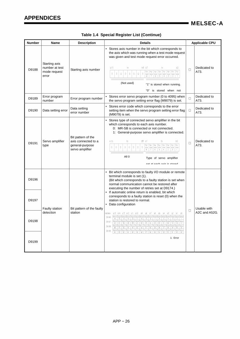
APPENDICES
APP − 26
MELSEC-A
Table 1.4 Special Register List (Continue)
Number Name Description Details Applicable CPU
D9188
Starting axis number at test mode request error
Starting axis number
• Stores axis number in the bit which corresponds to the axis which was running when a test mode request was given and test mode request error occurred.
Dedicated to A73.
D9189 Error program number Error program number • Stores error servo program number (0 to 4095) when
the servo program setting error flag (M9079) is set. Dedicated to A73.
D9190 Data setting error Data setting error number
• Stores error code which corresponds to the error setting item when the servo program setting error flag (M9079) is set.
Dedicated to A73.
D9191 Servo amplifier type
Bit pattern of the axis connected to a general-purpose servo amplifier
• Stores type of connected servo amplifier in the bit which corresponds to each axis number. 0: MR-SB is connected or not connected. 1: General-purpose servo amplifier is connected.
Dedicated to A73.
D9196
D9197
D9198
D9199
Faulty station detection
Bit pattern of the faulty station
• Bit which corresponds to faulty I/O module or remote terminal module is set (1). (Bit which corresponds to a faulty station is set when normal communication cannot be restored after executing the number of retries set at D9174.)
• If automatic online return is enabled, bit which corresponds to a faulty station is reset (0) when the station is restored to normal.
• Data configuration
Usable with A2C and A52G.
1: Error
0 N l
(Not used) "1" is stored when running.
"0" is stored when not
All 0 Type of servo amplifier
set at each axis is stored
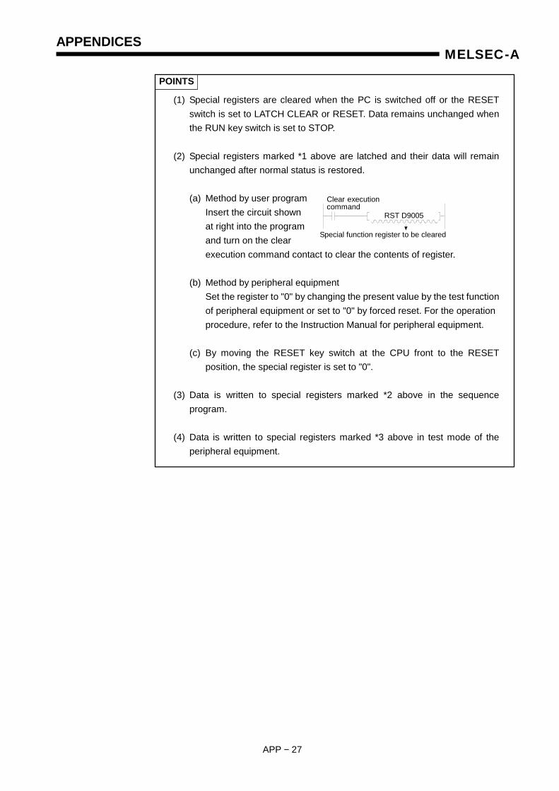
APPENDICES
APP − 27
MELSEC-A
POINTS
(1) Special registers are cleared when the PC is switched off or the RESET switch is set to LATCH CLEAR or RESET. Data remains unchanged when the RUN key switch is set to STOP.
(2) Special registers marked *1 above are latched and their data will remain
unchanged after normal status is restored.
(a) Method by user program Insert the circuit shown at right into the program and turn on the clear execution command contact to clear the contents of register.
(b) Method by peripheral equipment
Set the register to "0" by changing the present value by the test function of peripheral equipment or set to "0" by forced reset. For the operation procedure, refer to the Instruction Manual for peripheral equipment.
(c) By moving the RESET key switch at the CPU front to the RESET
position, the special register is set to "0". (3) Data is written to special registers marked *2 above in the sequence
program. (4) Data is written to special registers marked *3 above in test mode of the
peripheral equipment.
RST D9005
Special function register to be cleared
Clear executioncommand
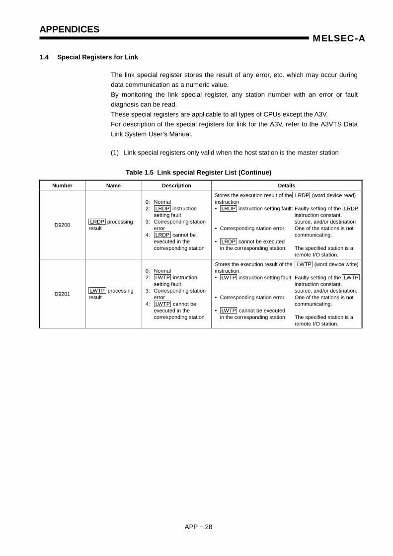
APPENDICES
APP − 28
MELSEC-A
1.4 Special Registers for Link
The link special register stores the result of any error, etc. which may occur during data communication as a numeric value. By monitoring the link special register, any station number with an error or fault diagnosis can be read. These special registers are applicable to all types of CPUs except the A3V. For description of the special registers for link for the A3V, refer to the A3VTS Data Link System User’s Manual.
(1) Link special registers only valid when the host station is the master station Table 1.5 Link special Register List (Continue)
Number Name Description Details
D9200 LRDP processing result
0: Normal 2: LRDP instruction setting fault 3: Corresponding station error 4: LRDP cannot be executed in the corresponding station
Stores the execution result of the LRDP (word device read) instruction • LRDP instruction setting fault: Faulty setting of the LRDP instruction constant, source, and/or destination• Corresponding station error: One of the stations is not communicating. • LRDP cannot be executed in the corresponding station: The specified station is a remote I/O station.
D9201 LWTP processing result
0: Normal 2: LWTP instruction setting fault 3: Corresponding station error 4: LWTP cannot be executed in the corresponding station
Stores the execution result of the LWTP (word device write) instruction. • LWTP instruction setting fault: Faulty setting of the LWTP instruction constant, source, and/or destination.• Corresponding station error: One of the stations is not communicating. • LWTP cannot be executed in the corresponding station: The specified station is a remote I/O station.
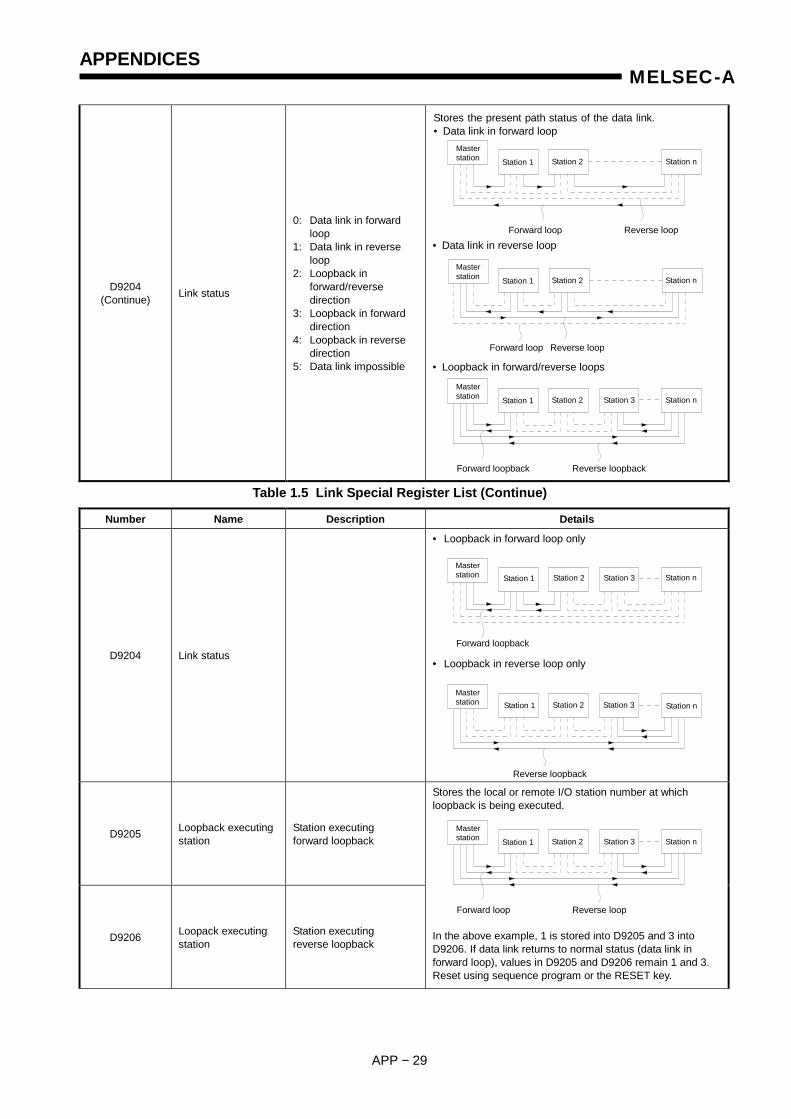
APPENDICES
APP − 29
MELSEC-A
D9204 (Continue) Link status
0: Data link in forward loop 1: Data link in reverse loop 2: Loopback in forward/reverse direction 3: Loopback in forward direction 4: Loopback in reverse direction 5: Data link impossible
Table 1.5 Link Special Register List (Continue)
Number Name Description Details
D9204 Link status
• Loopback in forward loop only
• Loopback in reverse loop only
D9205 Loopback executing station
Station executing forward loopback
D9206 Loopack executing station
Station executing reverse loopback
Stores the local or remote I/O station number at which loopback is being executed.
In the above example, 1 is stored into D9205 and 3 into D9206. If data link returns to normal status (data link in forward loop), values in D9205 and D9206 remain 1 and 3. Reset using sequence program or the RESET key.
Stores the present path status of the data link.• Data link in forward loop
Forward loop Reverse loop
• Data link in reverse loop
• Loopback in forward/reverse loops
Forward loop Reverse loop
Masterstation Station 1 Station 2 Station n
Masterstation Station 1 Station 2 Station n
Forward loopback Reverse loopback
Masterstation Station 1 Station 2 Station nStation 3
Reverse loopback
Forward loopback
Masterstation Station 1 Station 2 Station nStation 3
Masterstation Station 1 Station 2 Station nStation 3
Forward loop Reverse loop
Masterstation Station 1 Station 2 Station nStation 3
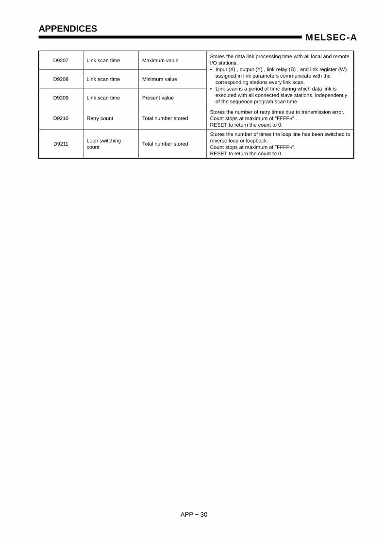
APPENDICES
APP − 30
MELSEC-A
D9207 Link scan time Maximum value
D9208 Link scan time Minimum value
D9209 Link scan time Present value
Stores the data link processing time with all local and remote I/O stations. • Input (X) , output (Y) , link relay (B) , and link register (W) assigned in link parameters communicate with the corresponding stations every link scan. • Link scan is a period of time during which data link is executed with all connected slave stations, independently of the sequence program scan time
D9210 Retry count Total number stored Stores the number of retry times due to transmission error. Count stops at maximum of "FFFFH" . RESET to return the count to 0.
D9211 Loop switching count Total number stored
Stores the number of times the loop line has been switched to reverse loop or loopback. Count stops at maximum of "FFFFH". RESET to return the count to 0.
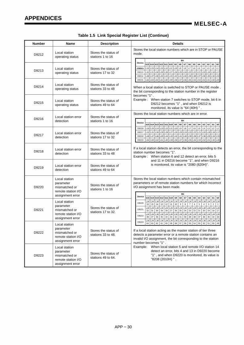
APPENDICES
APP − 30
MELSEC-A
Table 1.5 Link Special Register List (Continue)
Number Name Description Details
D9212 Local station operating status
Stores the status of stations 1 to 16
D9213 Local station operating status
Stores the status of stations 17 to 32
D9214 Local station operating status
Stores the status of stations 33 to 48
D9215 Local station operating status
Stores the status of stations 49 to 64
Stores the local station numbers which are in STOP or PAUSE mode.
When a local station is switched to STOP or PAUSE mode , the bit corresponding to the station number in the register becomes "1" . Example : When station 7 switches to STOP mode, bit 6 in D9212 becomes "1" , and when D9212 is monitored, its value is "64 (40H) " .
D9216 Local station error detection
Stores the status of stations 1 to 16
D9217 Local station error detection
Stores the status of stations 17 to 32
D9218 Local station error detection
Stores the status of stations 33 to 48
D9219 Local station error detection
Stores the status of stations 49 to 64
Stores the local station numbers which are in error.
If a local station detects an error, the bit corresponding to the station number becomes "1". Example : When station 6 and 12 detect an error, bits 5 and 11 in D9216 become "1", and when D9216 is monitored, its value is "2080 (820H)".
D9220
Local station parameter mismatched or remote station I/O assignment error
Stores the status of stations 1 to 16
D9221
Local station parameter mismatched or remote station I/O assignment error
Stores the status of stations 17 to 32.
D9222
Local station parameter mismatched or remote station I/O assignment error
Stores the status of stations 33 to 48.
D9223
Local station parameter mismatched or remote station I/O assignment error
Stores the status of stations 49 to 64.
Stores the local station numbers which contain mismatched parameters or of remote station numbers for which incorrect I/O assignment has been made.
If a local station acting as the master station of tier three detects a parameter error or a remote station contains an invalid I/O assignment, the bit corresponding to the station number becomes "1" . Example: When local station 5 and remote I/O station 14 detect an error, bits 4 and 13 in D9220 become "1" , and when D9220 is monitored, its value is "8208 (2010H) " .
Bit
b15 b14 b13 b12 b11 b10 b9 b8 b7 b6 b5 b4 b3 b2 b1 b0
D9220 L/R16
L/R15
L/R14
L/R13
L/R12
L/R 11
L/R 10
L/R 9
L/R 8
L/R 7
L/R 6
L/R 5
L/R4
L/R3
L/R2
L/R1
D9221 L/R32
L/R31
L/R30
L/R29
L/R28
L/R 27
L/R 26
L/R 25
L/R 24
L/R 23
L/R 22
L/R 21
L/R20
L/R19
L/R18
L/R17
D9222 L/R48
L/R47
L/R46
L/R45
L/R44
L/R 43
L/R 42
L/R 41
L/R 40
L/R 39
L/R 38
L/R 37
L/R36
L/R35
L/R34
L/R33
D9223 L/R64
L/R63
L/R62
L/R61
L/R60
L/R 59
L/R 58
L/R 57
L/R 56
L/R 55
L/R 54
L/R 53
L/R52
L/R51
L/R50
L/R49
Device
b
Bit
b15 b14 b13 b12 b11 b10 b9 b8 b7 b6 b5 b4 b3 b2 b1 b0
D9216 L16 L15 L14 L13 L12 L11 L10 L9 L8 L7 L6 L5 L4 L3 L2 L1
D9217 L32 L31 L30 L29 L28 L27 L26 L25 L24 L23 L22 L21 L20 L19 L18 L17
D9218 L48 L47 L46 L45 L44 L43 L42 L41 L40 L39 L38 L37 L36 L35 L34 L33
D9219 L64 L63 L62 L61 L60 L59 L58 L57 L56 L55 L54 L53 L52 L51 L50 L49
Device
Bit
b15 b14 b13 b12 b11 b10 b9 b8 b7 b6 b5 b4 b3 b2 b1 b0
D9212 L16 L15 L14 L13 L12 L11 L10 L9 L8 L7 L6 L5 L4 L3 L2 L1
D9213 L32 L31 L30 L29 L28 L27 L26 L25 L24 L23 L22 L21 L20 L19 L18 L17
D9214 L48 L47 L46 L45 L44 L43 L42 L41 L40 L39 L38 L37 L36 L35 L34 L33
D9215 L64 L63 L62 L61 L60 L59 L58 L57 L56 L55 L54 L53 L52 L51 L50 L49
Device
number
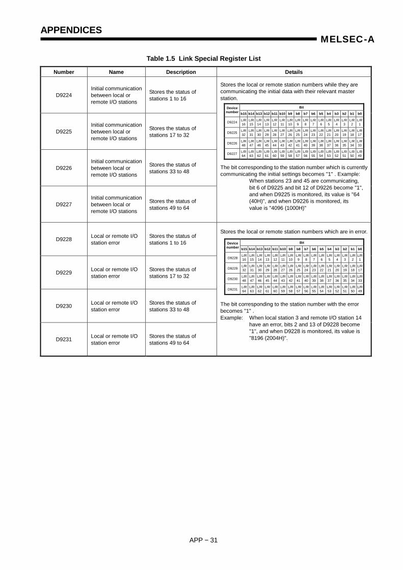
APPENDICES
APP − 31
MELSEC-A
Table 1.5 Link Special Register List
Number Name Description Details
D9224 Initial communication between local or remote I/O stations
Stores the status of stations 1 to 16
D9225 Initial communication between local or remote I/O stations
Stores the status of stations 17 to 32
D9226 Initial communication between local or remote I/O stations
Stores the status of stations 33 to 48
D9227 Initial communication between local or remote I/O stations
Stores the status of stations 49 to 64
Stores the local or remote station numbers while they are communicating the initial data with their relevant master station.
The bit corresponding to the station number which is currently communicating the initial settings becomes "1" . Example: When stations 23 and 45 are communicating, bit 6 of D9225 and bit 12 of D9226 become "1", and when D9225 is monitored, its value is "64 (40H)", and when D9226 is monitored, its value is "4096 (1000H)"
D9228 Local or remote I/O station error
Stores the status of stations 1 to 16
D9229 Local or remote I/O station error
Stores the status of stations 17 to 32
D9230 Local or remote I/O station error
Stores the status of stations 33 to 48
D9231 Local or remote I/O station error
Stores the status of stations 49 to 64
Stores the local or remote station numbers which are in error.
The bit corresponding to the station number with the error becomes "1" . Example: When local station 3 and remote I/O station 14 have an error, bits 2 and 13 of D9228 become "1", and when D9228 is monitored, its value is "8196 (2004H)".
Bit Devicenumber b15 b14 b13 b12 b11 b10 b9 b8 b7 b6 b5 b4 b3 b2 b1 b0
D9224 L/R16
L/R15
L/R14
L/R13
L/R12
L/R 11
L/R 10
L/R 9
L/R 8
L/R 7
L/R 6
L/R 5
L/R4
L/R3
L/R2
L/R1
D9225 L/R32
L/R31
L/R30
L/R29
L/R28
L/R 27
L/R 26
L/R 25
L/R 24
L/R 23
L/R 22
L/R 21
L/R20
L/R19
L/R18
L/R17
D9226 L/R48
L/R47
L/R46
L/R45
L/R44
L/R 43
L/R 42
L/R 41
L/R 40
L/R 39
L/R 38
L/R 37
L/R36
L/R35
L/R34
L/R33
D9227 L/R64
L/R63
L/R62
L/R61
L/R60
L/R 59
L/R 58
L/R 57
L/R 56
L/R 55
L/R 54
L/R 53
L/R52
L/R51
L/R50
L/R49
Bit Devicenumber b15 b14 b13 b12 b11 b10 b9 b8 b7 b6 b5 b4 b3 b2 b1 b0
D9228 L/R16
L/R15
L/R14
L/R13
L/R12
L/R 11
L/R 10
L/R 9
L/R 8
L/R 7
L/R 6
L/R 5
L/R4
L/R3
L/R2
L/R1
D9229 L/R32
L/R31
L/R30
L/R29
L/R28
L/R 27
L/R 26
L/R 25
L/R 24
L/R 23
L/R 22
L/R 21
L/R20
L/R19
L/R18
L/R17
D9230 L/R48
L/R47
L/R46
L/R45
L/R44
L/R 43
L/R 42
L/R 41
L/R 40
L/R 39
L/R 38
L/R 37
L/R36
L/R35
L/R34
L/R33
D9231 L/R64
L/R63
L/R62
L/R61
L/R60
L/R 59
L/R 58
L/R 57
L/R 56
L/R 55
L/R 54
L/R 53
L/R52
L/R51
L/R50
L/R49
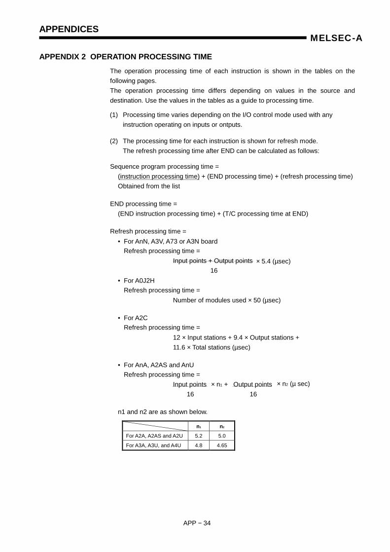
APPENDICES
APP − 34
MELSEC-A
APPENDIX 2 OPERATION PROCESSING TIME The operation processing time of each instruction is shown in the tables on the following pages. The operation processing time differs depending on values in the source and destination. Use the values in the tables as a guide to processing time.
(1) Processing time varies depending on the I/O control mode used with any instruction operating on inputs or ontputs.
(2) The processing time for each instruction is shown for refresh mode. The refresh processing time after END can be calculated as follows:
Sequence program processing time = (instruction processing time) + (END processing time) + (refresh processing time) Obtained from the list
END processing time = (END instruction processing time) + (T/C processing time at END)
Refresh processing time = • For AnN, A3V, A73 or A3N board Refresh processing time = Input points + Output points 16 • For A0J2H Refresh processing time = Number of modules used × 50 (µsec)
• For A2C Refresh processing time = 12 × Input stations + 9.4 × Output stations + 11.6 × Total stations (µsec)
• For AnA, A2AS and AnU Refresh processing time = Input points Output points 16 16
n1 and n2 are as shown below.
n1 n2
For A2A, A2AS and A2U 5.2 5.0
For A3A, A3U, and A4U 4.8 4.65
× 5.4 (µsec)
× n1 + × n2 (µ sec)
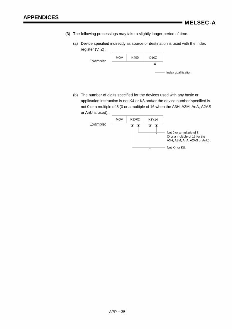
APPENDICES
APP − 35
MELSEC-A
(3) The following processings may take a slightly longer period of time.
(a) Device specified indirectly as source or destination is used with the index register (V, Z) . Example:
(b) The number of digits specified for the devices used with any basic or application instruction is not K4 or K8 and/or the device number specified is not 0 or a multiple of 8 (0 or a multiple of 16 when the A3H, A3M, AnA, A2AS or AnU is used) . Example:
MOV K400 D10Z
Index qualification
MOV K3X02 K3Y14
Not 0 or a multiple of 8 (0 or a multiple of 16 for the A3H, A3M, AnA, A2AS or AnU) .
Not K4 or K8. •
•
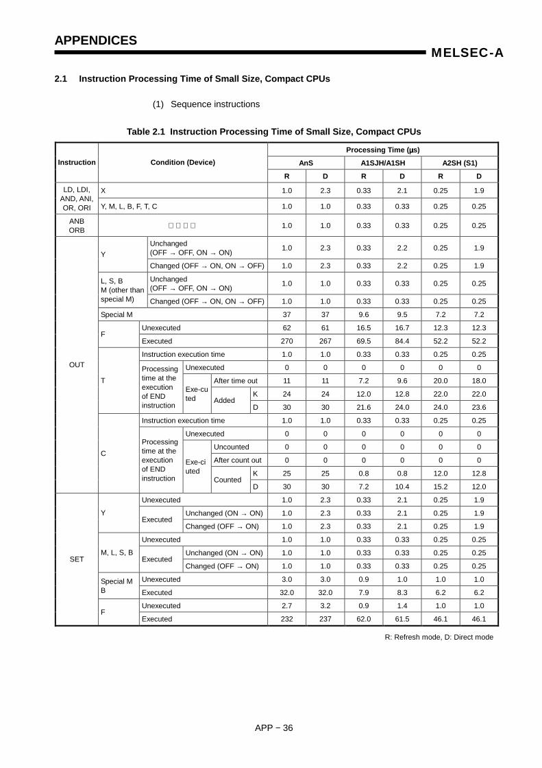
APPENDICES
APP − 36
MELSEC-A
2.1 Instruction Processing Time of Small Size, Compact CPUs
(1) Sequence instructions
Table 2.1 Instruction Processing Time of Small Size, Compact CPUs
Processing Time (µµµµs)
AnS A1SJH/A1SH A2SH (S1) Instruction Condition (Device)
R D R D R D
X 1.0 2.3 0.33 2.1 0.25 1.9 LD, LDI, AND, ANI, OR, ORI Y, M, L, B, F, T, C 1.0 1.0 0.33 0.33 0.25 0.25
ANB ORB 1.0 1.0 0.33 0.33 0.25 0.25
Unchanged (OFF → OFF, ON → ON) 1.0 2.3 0.33 2.2 0.25 1.9
Y Changed (OFF → ON, ON → OFF) 1.0 2.3 0.33 2.2 0.25 1.9
Unchanged (OFF → OFF, ON → ON) 1.0 1.0 0.33 0.33 0.25 0.25 L, S, B
M (other than special M) Changed (OFF → ON, ON → OFF) 1.0 1.0 0.33 0.33 0.25 0.25
Special M 37 37 9.6 9.5 7.2 7.2
Unexecuted 62 61 16.5 16.7 12.3 12.3 F
Executed 270 267 69.5 84.4 52.2 52.2
Instruction execution time 1.0 1.0 0.33 0.33 0.25 0.25
Unexecuted 0 0 0 0 0 0
After time out 11 11 7.2 9.6 20.0 18.0
K 24 24 12.0 12.8 22.0 22.0
T Processing time at the execution of END instruction
Exe-cuted Added
D 30 30 21.6 24.0 24.0 23.6
Instruction execution time 1.0 1.0 0.33 0.33 0.25 0.25
Unexecuted 0 0 0 0 0 0
Uncounted 0 0 0 0 0 0
After count out 0 0 0 0 0 0
K 25 25 0.8 0.8 12.0 12.8
OUT
C Processing time at the execution of END instruction
Exe-ciuted
Counted D 30 30 7.2 10.4 15.2 12.0
Unexecuted 1.0 2.3 0.33 2.1 0.25 1.9
Unchanged (ON → ON) 1.0 2.3 0.33 2.1 0.25 1.9 Y Executed
Changed (OFF → ON) 1.0 2.3 0.33 2.1 0.25 1.9
Unexecuted 1.0 1.0 0.33 0.33 0.25 0.25
Unchanged (ON → ON) 1.0 1.0 0.33 0.33 0.25 0.25 M, L, S, B Executed
Changed (OFF → ON) 1.0 1.0 0.33 0.33 0.25 0.25
Unexecuted 3.0 3.0 0.9 1.0 1.0 1.0 Special M B Executed 32.0 32.0 7.9 8.3 6.2 6.2
Unexecuted 2.7 3.2 0.9 1.4 1.0 1.0
SET
F Executed 232 237 62.0 61.5 46.1 46.1
R: Refresh mode, D: Direct mode
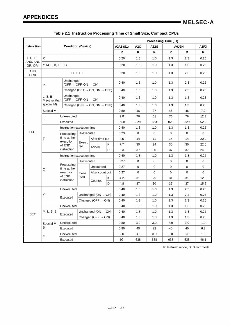
APPENDICES
APP − 37
MELSEC-A
Table 2.1 Instruction Processing Time of Small Size, Compact CPUs
Processing Time (µµµµs)
A2AS (S1) A2C A52G A0J2H A1FX Instruction Condition (Device)
R R R R D R
X 0.20 1.3 1.0 1.3 2.3 0.25 LD, LDI, AND, ANI, OR, ORI Y, M, L, B, F, T, C 0.20 1.3 1.0 1.3 1.0 0.25
ANB ORB 0.20 1.3 1.0 1.3 2.3 0.25
Unchanged (OFF → OFF, ON → ON) 0.40 1.3 1.0 1.3 2.3 0.25
Y Changed (OF F→ ON, ON → OFF) 0.40 1.3 1.0 1.3 2.3 0.25
Unchanged (OFF → OFF, ON → ON) 0.40 1.3 1.0 1.3 1.3 0.25 L, S, B
M (other than special M) Changed (OFF → ON, ON → OFF) 0.40 1.3 1.0 1.3 1.3 0.25
Special M 0.80 46 37 46 46 7.2
Unexecuted 2.8 76 61 76 76 12.3 F
Executed 99.0 829 663 829 829 52.2
Instruction execution time 0.40 1.3 1.0 1.3 1.3 0.25
Unexecuted 0.23 0 0 0 0 0
After time out 4.5 14 11 14 14 20.0
K 7.7 30 24 30 30 22.0
T Processing time at the execution of END instruction
Exe-cuted Added
D 8.3 37 30 37 37 24.0
Instruction execution time 0.40 1.3 1.0 1.3 1.3 0.25
Unexecuted 0.27 0 0 0 0 0
Uncounted 0.27 0 0 0 0 0
After count out 0.27 0 0 0 0 0
K 4.2 31 25 31 31 12.0
OUT
C Processing time at the execution of END instruction
Exe-ciuted
Counted D 4.8 37 30 37 37 15.2
Unexecuted 0.40 1.3 1.0 1.3 2.3 0.25
Unchanged (ON → ON) 0.40 1.3 1.0 1.3 2.3 0.25 Y Executed
Changed (OFF → ON) 0.40 1.3 1.0 1.3 2.3 0.25
Unexecuted 0.40 1.3 1.0 1.3 1.3 0.25
Unchanged (ON → ON) 0.40 1.3 1.0 1.3 1.3 0.25 M, L, S, B Executed
Changed (OFF → ON) 0.40 1.3 1.0 1.3 1.3 0.25
Unexecuted 0.80 3.0 3.0 3.0 3.0 1.0 Special M B Executed 0.80 40 32 40 40 6.2
Unexecuted 2.0 3.8 3.0 3.8 3.8 1.0
SET
F Executed 99 638 638 638 638 46.1
R: Refresh mode, D: Direct mode
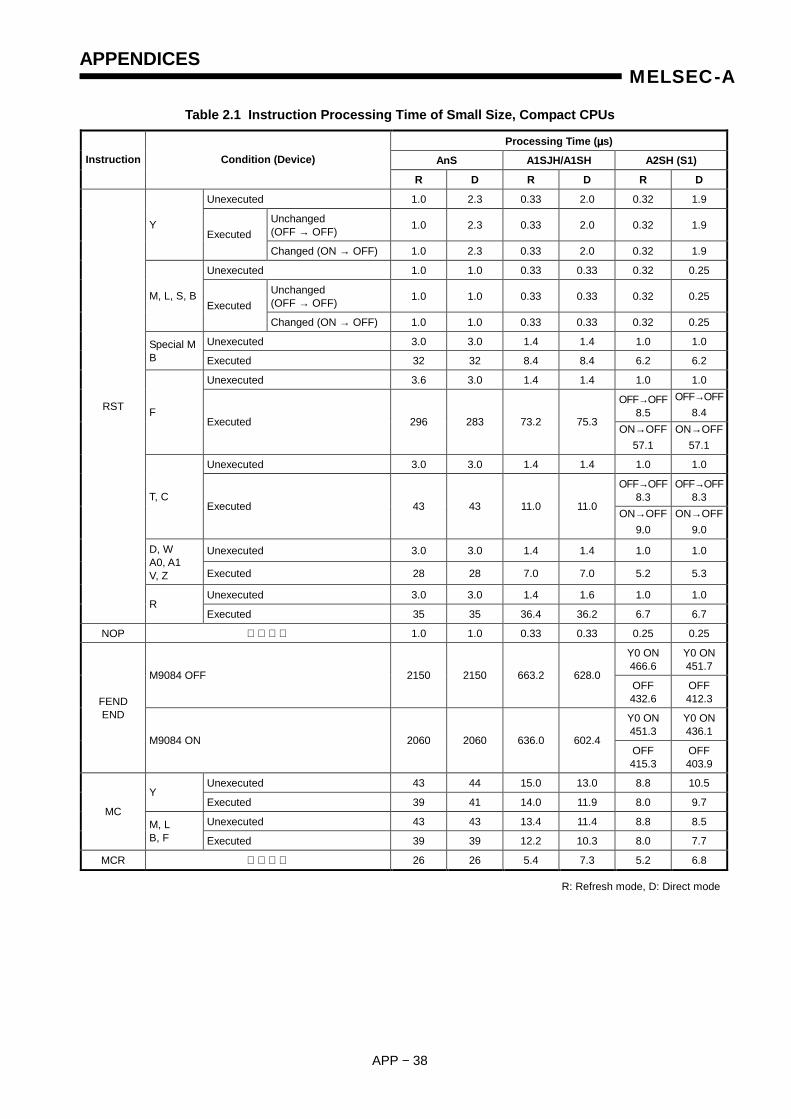
APPENDICES
APP − 38
MELSEC-A
Table 2.1 Instruction Processing Time of Small Size, Compact CPUs
Processing Time (µµµµs)
AnS A1SJH/A1SH A2SH (S1) Instruction Condition (Device)
R D R D R D
Unexecuted 1.0 2.3 0.33 2.0 0.32 1.9
Unchanged (OFF → OFF) 1.0 2.3 0.33 2.0 0.32 1.9 Y
Executed Changed (ON → OFF) 1.0 2.3 0.33 2.0 0.32 1.9
Unexecuted 1.0 1.0 0.33 0.33 0.32 0.25
Unchanged (OFF → OFF) 1.0 1.0 0.33 0.33 0.32 0.25 M, L, S, B
Executed Changed (ON → OFF) 1.0 1.0 0.33 0.33 0.32 0.25
Unexecuted 3.0 3.0 1.4 1.4 1.0 1.0 Special M B Executed 32 32 8.4 8.4 6.2 6.2
Unexecuted 3.6 3.0 1.4 1.4 1.0 1.0
OFF→OFF8.5
OFF→OFF8.4 F
Executed 296 283 73.2 75.3 ON→OFF
57.1 ON→OFF
57.1
Unexecuted 3.0 3.0 1.4 1.4 1.0 1.0
OFF→OFF8.3
OFF→OFF8.3 T, C
Executed 43 43 11.0 11.0 ON→OFF
9.0 ON→OFF
9.0
Unexecuted 3.0 3.0 1.4 1.4 1.0 1.0 D, W A0, A1 V, Z Executed 28 28 7.0 7.0 5.2 5.3
Unexecuted 3.0 3.0 1.4 1.6 1.0 1.0
RST
R Executed 35 35 36.4 36.2 6.7 6.7
NOP 1.0 1.0 0.33 0.33 0.25 0.25
Y0 ON466.6
Y0 ON451.7
M9084 OFF 2150 2150 663.2 628.0 OFF 432.6
OFF 412.3
Y0 ON451.3
Y0 ON436.1
FEND END
M9084 ON 2060 2060 636.0 602.4 OFF 415.3
OFF 403.9
Unexecuted 43 44 15.0 13.0 8.8 10.5 Y
Executed 39 41 14.0 11.9 8.0 9.7
Unexecuted 43 43 13.4 11.4 8.8 8.5 MC
M, L B, F Executed 39 39 12.2 10.3 8.0 7.7
MCR 26 26 5.4 7.3 5.2 6.8
R: Refresh mode, D: Direct mode
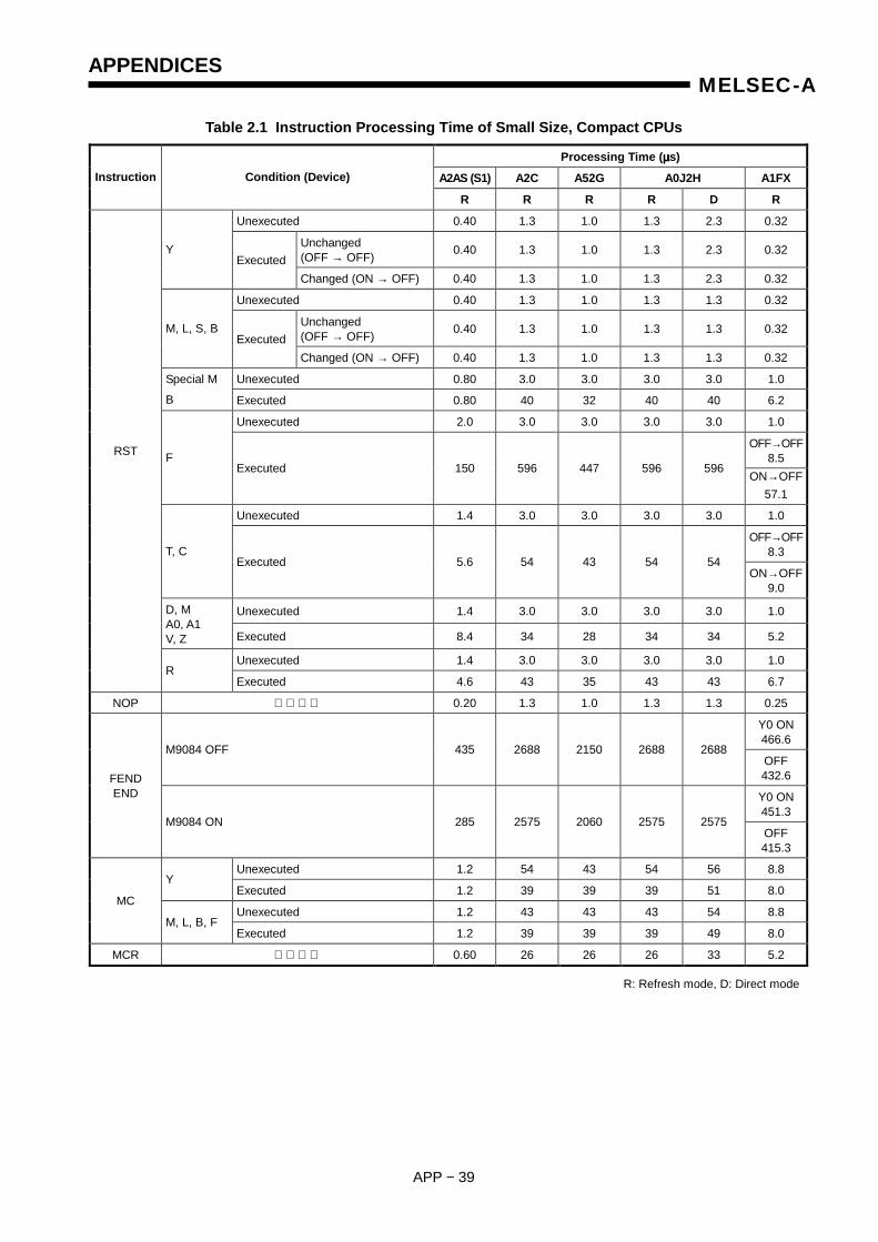
APPENDICES
APP − 39
MELSEC-A
Table 2.1 Instruction Processing Time of Small Size, Compact CPUs
Processing Time (µµµµs)
A2AS (S1) A2C A52G A0J2H A1FX Instruction Condition (Device)
R R R R D R
Unexecuted 0.40 1.3 1.0 1.3 2.3 0.32
Unchanged (OFF → OFF) 0.40 1.3 1.0 1.3 2.3 0.32 Y
Executed Changed (ON → OFF) 0.40 1.3 1.0 1.3 2.3 0.32
Unexecuted 0.40 1.3 1.0 1.3 1.3 0.32
Unchanged (OFF → OFF) 0.40 1.3 1.0 1.3 1.3 0.32 M, L, S, B
Executed Changed (ON → OFF) 0.40 1.3 1.0 1.3 1.3 0.32
Unexecuted 0.80 3.0 3.0 3.0 3.0 1.0 Special M
B Executed 0.80 40 32 40 40 6.2
Unexecuted 2.0 3.0 3.0 3.0 3.0 1.0
OFF→OFF8.5 F
Executed 150 596 447 596 596 ON→OFF
57.1
Unexecuted 1.4 3.0 3.0 3.0 3.0 1.0
OFF→OFF8.3 T, C
Executed 5.6 54 43 54 54 ON→OFF
9.0
Unexecuted 1.4 3.0 3.0 3.0 3.0 1.0 D, M A0, A1 V, Z Executed 8.4 34 28 34 34 5.2
Unexecuted 1.4 3.0 3.0 3.0 3.0 1.0
RST
R Executed 4.6 43 35 43 43 6.7
NOP 0.20 1.3 1.0 1.3 1.3 0.25
Y0 ON466.6
M9084 OFF 435 2688 2150 2688 2688 OFF 432.6
Y0 ON451.3
FEND END
M9084 ON 285 2575 2060 2575 2575 OFF 415.3
Unexecuted 1.2 54 43 54 56 8.8 Y
Executed 1.2 39 39 39 51 8.0
Unexecuted 1.2 43 43 43 54 8.8 MC
M, L, B, F Executed 1.2 39 39 39 49 8.0
MCR 0.60 26 26 26 33 5.2
R: Refresh mode, D: Direct mode
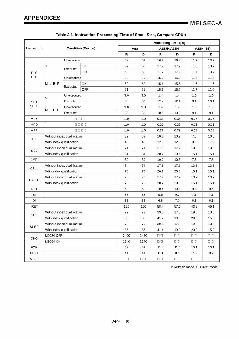
APPENDICES
APP − 40
MELSEC-A
Table 2.1 Instruction Processing Time of Small Size, Compact CPUs
Processing Time (µµµµs)
AnS A1SJH/A1SH A2SH (S1) Instruction Condition (Device)
R D R D R D
Unexecuted 59 61 16.8 16.8 11.7 13.7
ON 62 63 17.2 17.2 11.6 13.7 Y Executed
OFF 60 62 17.2 17.2 11.7 13.7
Unexecuted 59 59 15.2 15.2 11.7 11.7
ON 62 62 15.6 15.6 11.6 11.6
PLS PLF
M, L, B, F Executed
OFF 61 61 15.6 15.6 11.7 11.6
Unexecuted 3.0 3.0 1.4 1.4 1.0 1.0 Y
Executed 38 39 12.4 12.4 8.1 10.1
Unexecuted 3.0 3.0 1.4 1.4 1.0 1.0 SET
SFTP M, L, B, F
Executed 38 38 10.8 10.8 8.1 8.1
MPS 1.0 1.0 0.33 0.33 0.25 0.25
MRD 1.0 1.0 0.33 0.33 0.25 0.25
MPP 1.0 1.0 0.33 0.33 0.25 0.25
Without index qualification 39 39 10.2 10.2 7.6 10.0 CJ
With index qualification 48 48 12.6 12.6 9.5 11.9
Without index qualification 71 71 17.8 17.7 13.3 13.3 SCJ
With index qualification 81 81 20.2 20.5 15.1 15.1
JMP 39 39 10.2 10.3 7.6 7.6
Without index qualification 74 74 17.8 17.9 13.3 13.3 CALL
With index qualification 78 78 20.2 20.3 15.1 15.1
Without index qualification 70 70 17.8 17.9 13.2 13.2 CALLP
With index qualification 78 78 20.2 20.3 15.1 15.1
RET 50 50 10.4 10.3 9.3 9.6
EI 38 38 9.6 9.2 7.1 7.1
DI 66 66 6.8 7.0 6.5 6.5
IRET 120 120 58.4 57.6 43.2 45.1
Without index qualification 79 79 39.8 17.6 19.0 13.0 SUB
With index qualification 85 85 41.4 19.2 20.0 15.0
Without index qualification 79 79 39.8 17.6 19.0 13.0 SUBP
With index qualification 85 85 41.4 19.2 20.0 15.0
M9084 OFF 2420 2420 CHG
M9084 ON 2340 2340
FOR 53 53 11.4 11.6 10.1 10.1
NEXT 41 41 8.0 8.1 7.5 8.2
STOP
R: Refresh mode, D: Direct mode
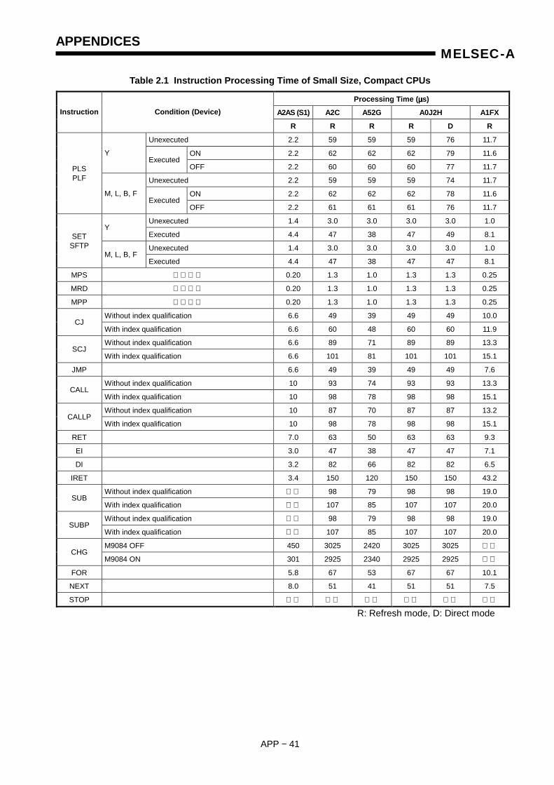
APPENDICES
APP − 41
MELSEC-A
Table 2.1 Instruction Processing Time of Small Size, Compact CPUs
Processing Time (µµµµs)
A2AS (S1) A2C A52G A0J2H A1FX Instruction Condition (Device)
R R R R D R
Unexecuted 2.2 59 59 59 76 11.7
ON 2.2 62 62 62 79 11.6 Y Executed
OFF 2.2 60 60 60 77 11.7
Unexecuted 2.2 59 59 59 74 11.7
ON 2.2 62 62 62 78 11.6
PLS PLF
M, L, B, F Executed
OFF 2.2 61 61 61 76 11.7
Unexecuted 1.4 3.0 3.0 3.0 3.0 1.0 Y
Executed 4.4 47 38 47 49 8.1
Unexecuted 1.4 3.0 3.0 3.0 3.0 1.0 SET
SFTP M, L, B, F
Executed 4.4 47 38 47 47 8.1
MPS 0.20 1.3 1.0 1.3 1.3 0.25
MRD 0.20 1.3 1.0 1.3 1.3 0.25
MPP 0.20 1.3 1.0 1.3 1.3 0.25
Without index qualification 6.6 49 39 49 49 10.0 CJ
With index qualification 6.6 60 48 60 60 11.9
Without index qualification 6.6 89 71 89 89 13.3 SCJ
With index qualification 6.6 101 81 101 101 15.1
JMP 6.6 49 39 49 49 7.6
Without index qualification 10 93 74 93 93 13.3 CALL
With index qualification 10 98 78 98 98 15.1
Without index qualification 10 87 70 87 87 13.2 CALLP
With index qualification 10 98 78 98 98 15.1
RET 7.0 63 50 63 63 9.3
EI 3.0 47 38 47 47 7.1
DI 3.2 82 66 82 82 6.5
IRET 3.4 150 120 150 150 43.2
Without index qualification 98 79 98 98 19.0 SUB
With index qualification 107 85 107 107 20.0
Without index qualification 98 79 98 98 19.0 SUBP
With index qualification 107 85 107 107 20.0
M9084 OFF 450 3025 2420 3025 3025 CHG
M9084 ON 301 2925 2340 2925 2925
FOR 5.8 67 53 67 67 10.1
NEXT 8.0 51 41 51 51 7.5
STOP
R: Refresh mode, D: Direct mode
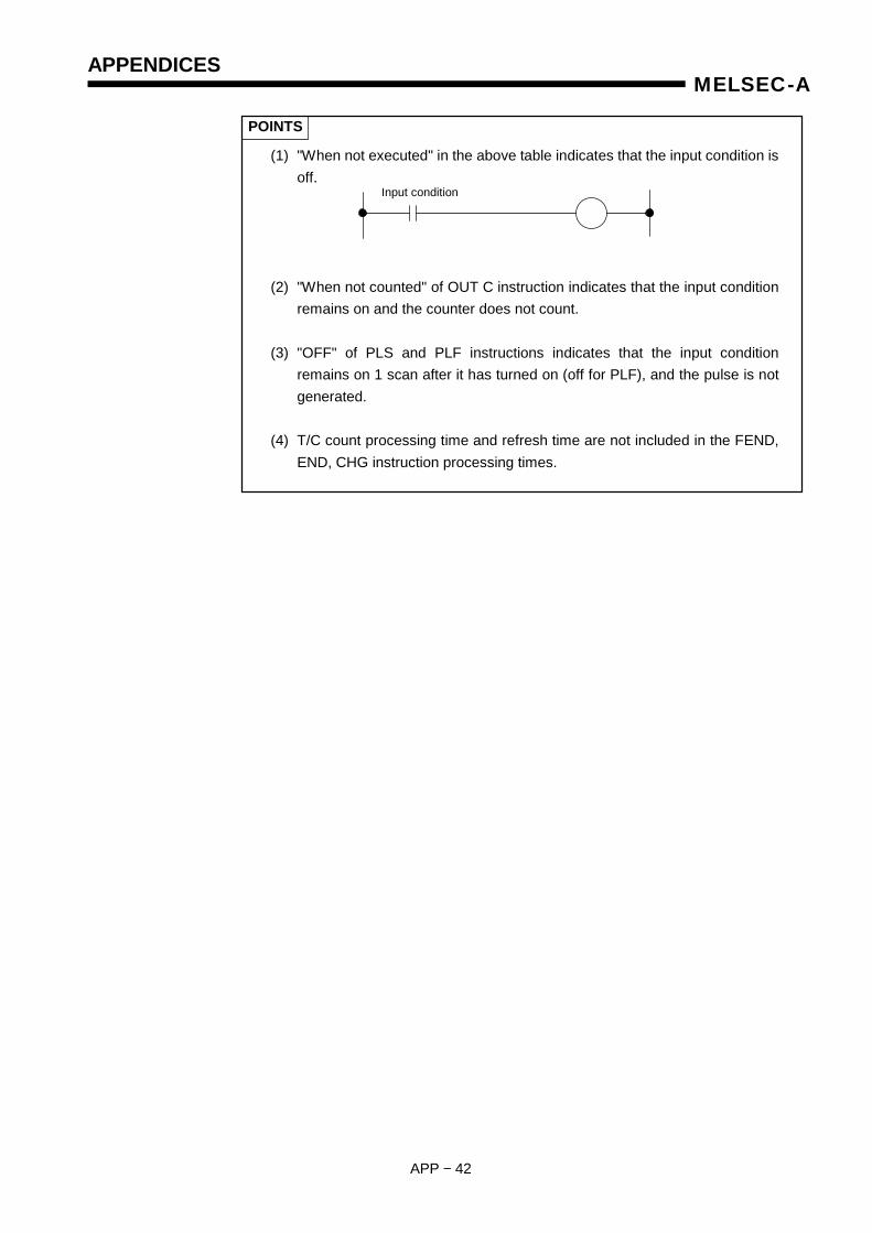
APPENDICES
APP − 42
MELSEC-A
POINTS
(1) "When not executed" in the above table indicates that the input condition is off.
(2) "When not counted" of OUT C instruction indicates that the input condition
remains on and the counter does not count. (3) "OFF" of PLS and PLF instructions indicates that the input condition
remains on 1 scan after it has turned on (off for PLF), and the pulse is not generated.
(4) T/C count processing time and refresh time are not included in the FEND,
END, CHG instruction processing times.
Input condition
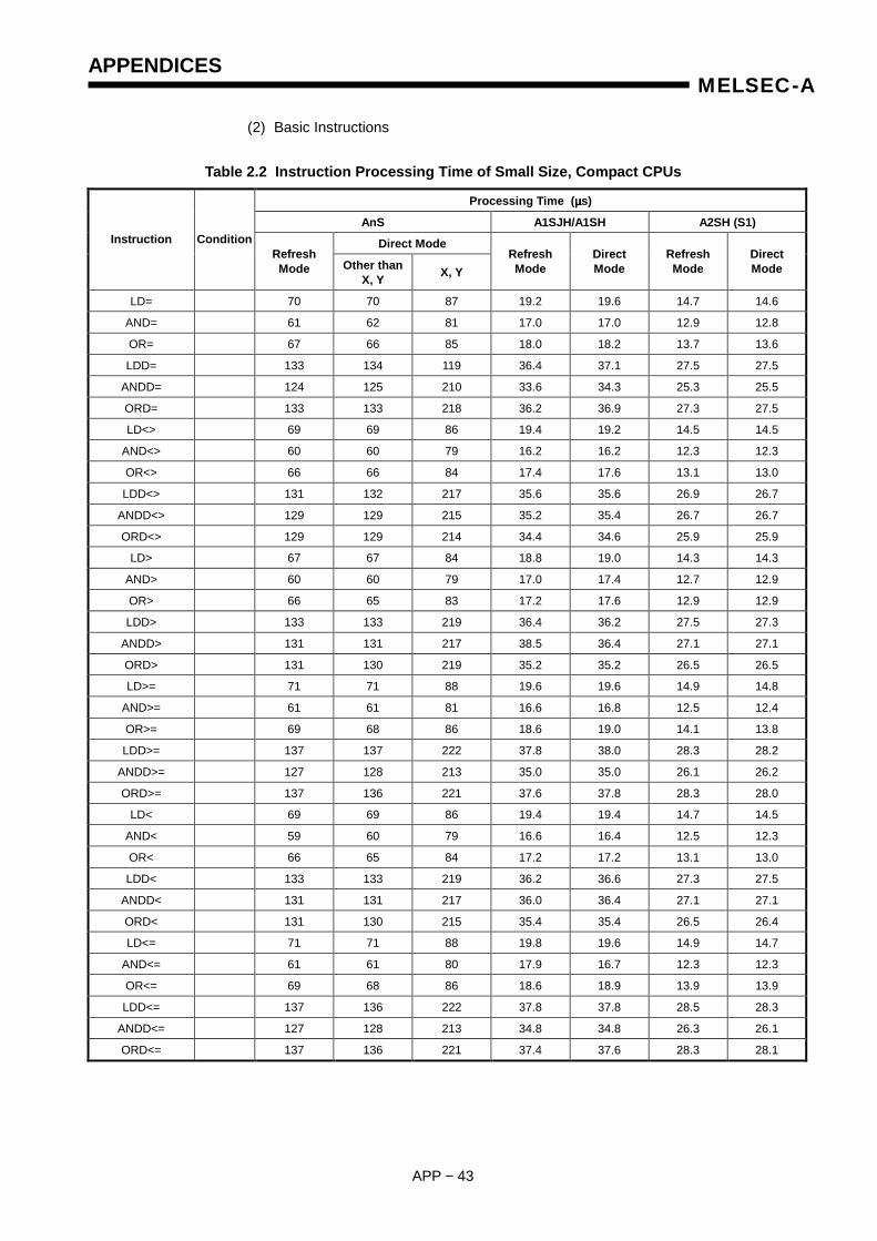
APPENDICES
APP − 43
MELSEC-A
(2) Basic Instructions
Table 2.2 Instruction Processing Time of Small Size, Compact CPUs
Processing Time (µµµµs)
AnS A1SJH/A1SH A2SH (S1)
Direct Mode Instruction Condition Refresh Mode Other than
X, Y X, Y Refresh Mode
Direct Mode
Refresh Mode
Direct Mode
LD= 70 70 87 19.2 19.6 14.7 14.6
AND= 61 62 81 17.0 17.0 12.9 12.8
OR= 67 66 85 18.0 18.2 13.7 13.6
LDD= 133 134 119 36.4 37.1 27.5 27.5
ANDD= 124 125 210 33.6 34.3 25.3 25.5
ORD= 133 133 218 36.2 36.9 27.3 27.5
LD<> 69 69 86 19.4 19.2 14.5 14.5
AND<> 60 60 79 16.2 16.2 12.3 12.3
OR<> 66 66 84 17.4 17.6 13.1 13.0
LDD<> 131 132 217 35.6 35.6 26.9 26.7
ANDD<> 129 129 215 35.2 35.4 26.7 26.7
ORD<> 129 129 214 34.4 34.6 25.9 25.9
LD> 67 67 84 18.8 19.0 14.3 14.3
AND> 60 60 79 17.0 17.4 12.7 12.9
OR> 66 65 83 17.2 17.6 12.9 12.9
LDD> 133 133 219 36.4 36.2 27.5 27.3
ANDD> 131 131 217 38.5 36.4 27.1 27.1
ORD> 131 130 219 35.2 35.2 26.5 26.5
LD>= 71 71 88 19.6 19.6 14.9 14.8
AND>= 61 61 81 16.6 16.8 12.5 12.4
OR>= 69 68 86 18.6 19.0 14.1 13.8
LDD>= 137 137 222 37.8 38.0 28.3 28.2
ANDD>= 127 128 213 35.0 35.0 26.1 26.2
ORD>= 137 136 221 37.6 37.8 28.3 28.0
LD< 69 69 86 19.4 19.4 14.7 14.5
AND< 59 60 79 16.6 16.4 12.5 12.3
OR< 66 65 84 17.2 17.2 13.1 13.0
LDD< 133 133 219 36.2 36.6 27.3 27.5
ANDD< 131 131 217 36.0 36.4 27.1 27.1
ORD< 131 130 215 35.4 35.4 26.5 26.4
LD<= 71 71 88 19.8 19.6 14.9 14.7
AND<= 61 61 80 17.9 16.7 12.3 12.3
OR<= 69 68 86 18.6 18.9 13.9 13.9
LDD<= 137 136 222 37.8 37.8 28.5 28.3
ANDD<= 127 128 213 34.8 34.8 26.3 26.1
ORD<= 137 136 221 37.4 37.6 28.3 28.1
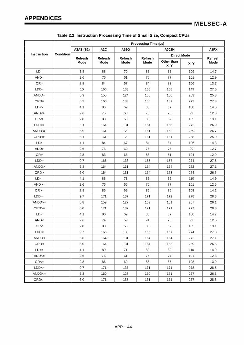
APPENDICES
APP − 44
MELSEC-A
Table 2.2 Instruction Processing Time of Small Size, Compact CPUs
Processing Time (µµµµs)
A2AS (S1) A2C A52G A0J2H A1FX
Direct Mode Instruction Condition Refresh Mode
Refresh Mode
Refresh Mode
Refresh Mode Other than
X, Y X, Y Refresh Mode
LD= 3.8 88 70 88 88 109 14.7
AND= 2.6 76 61 76 77 101 12.9
OR= 2.8 84 67 84 83 106 13.7
LDD= 10 166 133 166 168 149 27.5
ANDD= 5.9 155 124 155 156 263 25.3
ORD= 6.3 166 133 166 167 273 27.3
LD<> 4.1 86 69 86 87 108 14.5
AND<> 2.6 75 60 75 75 99 12.3
OR<> 2.8 83 66 83 82 105 13.1
LDD<> 10 164 131 164 166 272 26.9
ANDD<> 5.9 161 129 161 162 269 26.7
ORD<> 6.1 161 129 161 161 268 25.9
LD> 4.1 84 67 84 84 106 14.3
AND> 2.6 75 60 75 75 99 12.7
OR> 2.8 83 66 83 81 104 12.9
LDD> 9.7 166 133 166 167 274 27.5
ANDD> 5.8 164 131 164 164 272 27.1
ORD> 6.0 164 131 164 163 274 26.5
LD>= 4.1 88 71 88 89 110 14.9
AND>= 2.6 76 66 76 77 101 12.5
OR>= 2.8 86 69 86 86 108 14.1
LDD>= 9.7 171 137 171 172 278 28.3
ANDD>= 5.8 159 127 159 161 267 26.1
ORD>= 6.0 171 137 171 171 277 28.3
LD< 4.1 86 69 86 87 108 14.7
AND< 2.6 74 59 74 75 99 12.5
OR< 2.8 83 66 83 82 105 13.1
LDD< 9.7 166 133 166 167 274 27.3
ANDD< 5.8 164 131 164 164 272 27.1
ORD< 6.0 164 131 164 163 269 26.5
LD<= 4.1 89 71 89 89 110 14.9
AND<= 2.6 76 61 76 77 101 12.3
OR<= 2.8 86 69 86 85 108 13.9
LDD<= 9.7 171 137 171 171 278 28.5
ANDD<= 5.8 160 127 160 161 267 26.3
ORD<= 6.0 171 137 171 171 277 28.3
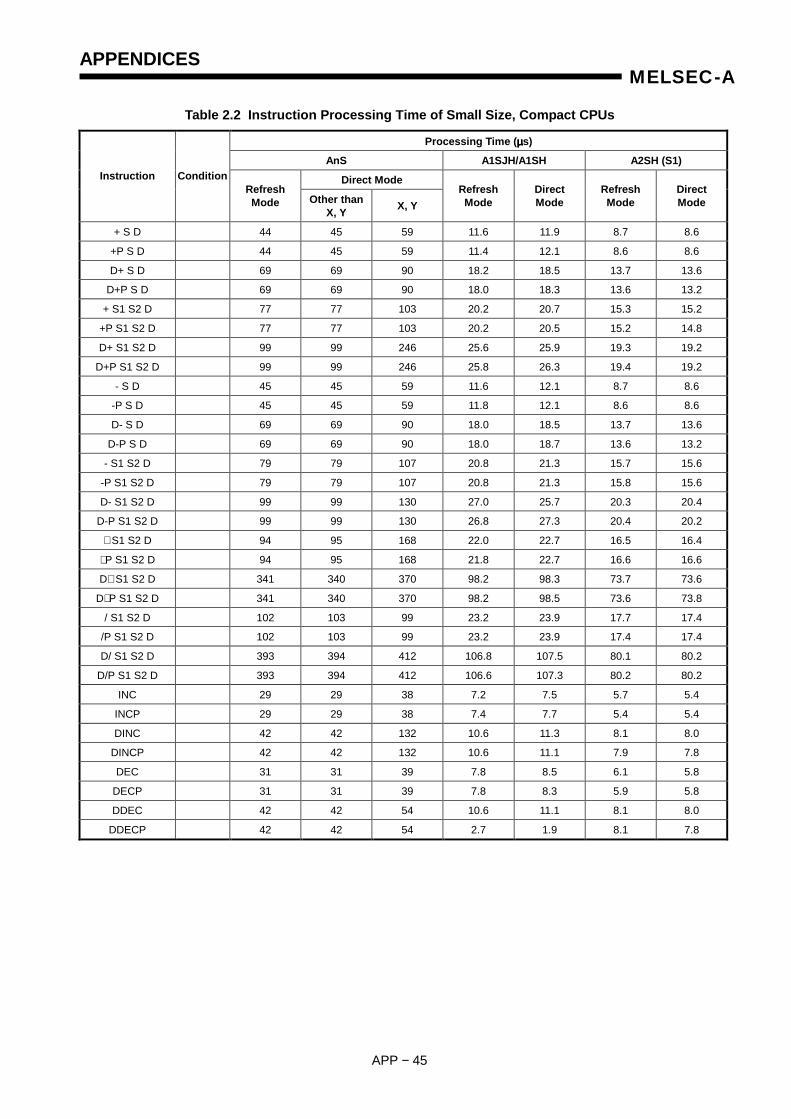
APPENDICES
APP − 45
MELSEC-A
Table 2.2 Instruction Processing Time of Small Size, Compact CPUs
Processing Time (µµµµs)
AnS A1SJH/A1SH A2SH (S1)
Direct Mode Instruction Condition Refresh Mode Other than
X, Y X, Y Refresh Mode
Direct Mode
Refresh Mode
Direct Mode
+ S D 44 45 59 11.6 11.9 8.7 8.6
+P S D 44 45 59 11.4 12.1 8.6 8.6
D+ S D 69 69 90 18.2 18.5 13.7 13.6
D+P S D 69 69 90 18.0 18.3 13.6 13.2
+ S1 S2 D 77 77 103 20.2 20.7 15.3 15.2
+P S1 S2 D 77 77 103 20.2 20.5 15.2 14.8
D+ S1 S2 D 99 99 246 25.6 25.9 19.3 19.2
D+P S1 S2 D 99 99 246 25.8 26.3 19.4 19.2
- S D 45 45 59 11.6 12.1 8.7 8.6
-P S D 45 45 59 11.8 12.1 8.6 8.6
D- S D 69 69 90 18.0 18.5 13.7 13.6
D-P S D 69 69 90 18.0 18.7 13.6 13.2
- S1 S2 D 79 79 107 20.8 21.3 15.7 15.6
-P S1 S2 D 79 79 107 20.8 21.3 15.8 15.6
D- S1 S2 D 99 99 130 27.0 25.7 20.3 20.4
D-P S1 S2 D 99 99 130 26.8 27.3 20.4 20.2
∗ S1 S2 D 94 95 168 22.0 22.7 16.5 16.4
∗ P S1 S2 D 94 95 168 21.8 22.7 16.6 16.6
D∗ S1 S2 D 341 340 370 98.2 98.3 73.7 73.6
D∗ P S1 S2 D 341 340 370 98.2 98.5 73.6 73.8
/ S1 S2 D 102 103 99 23.2 23.9 17.7 17.4
/P S1 S2 D 102 103 99 23.2 23.9 17.4 17.4
D/ S1 S2 D 393 394 412 106.8 107.5 80.1 80.2
D/P S1 S2 D 393 394 412 106.6 107.3 80.2 80.2
INC 29 29 38 7.2 7.5 5.7 5.4
INCP 29 29 38 7.4 7.7 5.4 5.4
DINC 42 42 132 10.6 11.3 8.1 8.0
DINCP 42 42 132 10.6 11.1 7.9 7.8
DEC 31 31 39 7.8 8.5 6.1 5.8
DECP 31 31 39 7.8 8.3 5.9 5.8
DDEC 42 42 54 10.6 11.1 8.1 8.0
DDECP 42 42 54 2.7 1.9 8.1 7.8
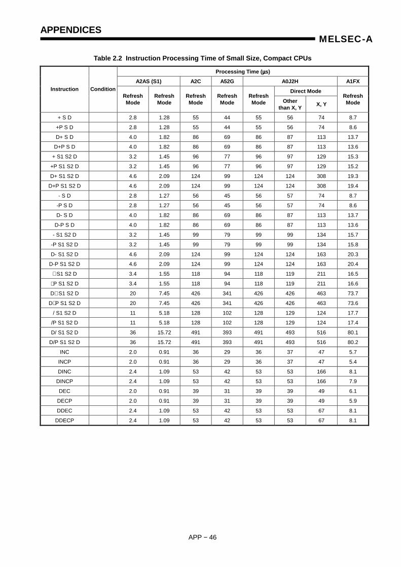
APPENDICES
APP − 46
MELSEC-A
Table 2.2 Instruction Processing Time of Small Size, Compact CPUs
Processing Time (µµµµs)
A2AS (S1) A2C A52G A0J2H A1FX
Direct Mode Instruction Condition Refresh Mode
Refresh Mode
Refresh Mode
Refresh Mode
Refresh Mode Other
than X, Y X, Y Refresh Mode
+ S D 2.8 1.28 55 44 55 56 74 8.7
+P S D 2.8 1.28 55 44 55 56 74 8.6
D+ S D 4.0 1.82 86 69 86 87 113 13.7
D+P S D 4.0 1.82 86 69 86 87 113 13.6
+ S1 S2 D 3.2 1.45 96 77 96 97 129 15.3
+P S1 S2 D 3.2 1.45 96 77 96 97 129 15.2
D+ S1 S2 D 4.6 2.09 124 99 124 124 308 19.3
D+P S1 S2 D 4.6 2.09 124 99 124 124 308 19.4
- S D 2.8 1.27 56 45 56 57 74 8.7
-P S D 2.8 1.27 56 45 56 57 74 8.6
D- S D 4.0 1.82 86 69 86 87 113 13.7
D-P S D 4.0 1.82 86 69 86 87 113 13.6
- S1 S2 D 3.2 1.45 99 79 99 99 134 15.7
-P S1 S2 D 3.2 1.45 99 79 99 99 134 15.8
D- S1 S2 D 4.6 2.09 124 99 124 124 163 20.3
D-P S1 S2 D 4.6 2.09 124 99 124 124 163 20.4
∗ S1 S2 D 3.4 1.55 118 94 118 119 211 16.5
∗ P S1 S2 D 3.4 1.55 118 94 118 119 211 16.6
D∗ S1 S2 D 20 7.45 426 341 426 426 463 73.7
D∗ P S1 S2 D 20 7.45 426 341 426 426 463 73.6
/ S1 S2 D 11 5.18 128 102 128 129 124 17.7
/P S1 S2 D 11 5.18 128 102 128 129 124 17.4
D/ S1 S2 D 36 15.72 491 393 491 493 516 80.1
D/P S1 S2 D 36 15.72 491 393 491 493 516 80.2
INC 2.0 0.91 36 29 36 37 47 5.7
INCP 2.0 0.91 36 29 36 37 47 5.4
DINC 2.4 1.09 53 42 53 53 166 8.1
DINCP 2.4 1.09 53 42 53 53 166 7.9
DEC 2.0 0.91 39 31 39 39 49 6.1
DECP 2.0 0.91 39 31 39 39 49 5.9
DDEC 2.4 1.09 53 42 53 53 67 8.1
DDECP 2.4 1.09 53 42 53 53 67 8.1
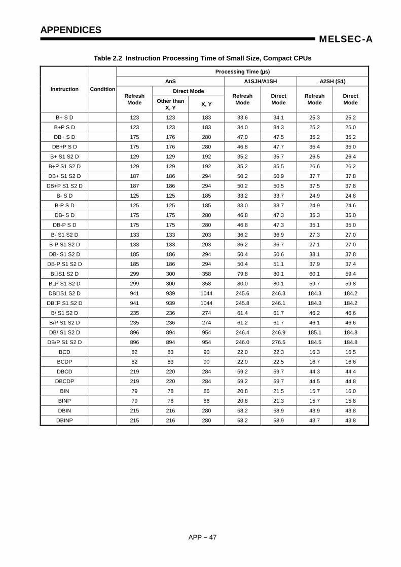
APPENDICES
APP − 47
MELSEC-A
Table 2.2 Instruction Processing Time of Small Size, Compact CPUs
Processing Time (µµµµs)
AnS A1SJH/A1SH A2SH (S1)
Direct Mode Instruction Condition Refresh Mode Other than
X, Y X, Y Refresh Mode
Direct Mode
Refresh Mode
Direct Mode
B+ S D 123 123 183 33.6 34.1 25.3 25.2
B+P S D 123 123 183 34.0 34.3 25.2 25.0
DB+ S D 175 176 280 47.0 47.5 35.2 35.2
DB+P S D 175 176 280 46.8 47.7 35.4 35.0
B+ S1 S2 D 129 129 192 35.2 35.7 26.5 26.4
B+P S1 S2 D 129 129 192 35.2 35.5 26.6 26.2
DB+ S1 S2 D 187 186 294 50.2 50.9 37.7 37.8
DB+P S1 S2 D 187 186 294 50.2 50.5 37.5 37.8
B- S D 125 125 185 33.2 33.7 24.9 24.8
B-P S D 125 125 185 33.0 33.7 24.9 24.6
DB- S D 175 175 280 46.8 47.3 35.3 35.0
DB-P S D 175 175 280 46.8 47.3 35.1 35.0
B- S1 S2 D 133 133 203 36.2 36.9 27.3 27.0
B-P S1 S2 D 133 133 203 36.2 36.7 27.1 27.0
DB- S1 S2 D 185 186 294 50.4 50.6 38.1 37.8
DB-P S1 S2 D 185 186 294 50.4 51.1 37.9 37.4
B∗ S1 S2 D 299 300 358 79.8 80.1 60.1 59.4
B∗ P S1 S2 D 299 300 358 80.0 80.1 59.7 59.8
DB∗ S1 S2 D 941 939 1044 245.6 246.3 184.3 184.2
DB∗ P S1 S2 D 941 939 1044 245.8 246.1 184.3 184.2
B/ S1 S2 D 235 236 274 61.4 61.7 46.2 46.6
B/P S1 S2 D 235 236 274 61.2 61.7 46.1 46.6
DB/ S1 S2 D 896 894 954 246.4 246.9 185.1 184.8
DB/P S1 S2 D 896 894 954 246.0 276.5 184.5 184.8
BCD 82 83 90 22.0 22.3 16.3 16.5
BCDP 82 83 90 22.0 22.5 16.7 16.6
DBCD 219 220 284 59.2 59.7 44.3 44.4
DBCDP 219 220 284 59.2 59.7 44.5 44.8
BIN 79 78 86 20.8 21.5 15.7 16.0
BINP 79 78 86 20.8 21.3 15.7 15.8
DBIN 215 216 280 58.2 58.9 43.9 43.8
DBINP 215 216 280 58.2 58.9 43.7 43.8
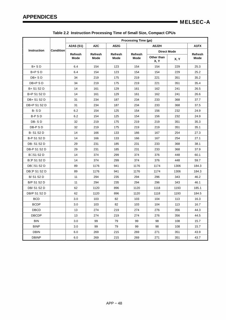
APPENDICES
APP − 48
MELSEC-A
Table 2.2 Instruction Processing Time of Small Size, Compact CPUs
Processing Time (µµµµs)
A2AS (S1) A2C A52G A0J2H A1FX
Direct Mode Instruction Condition Refresh Mode
Refresh Mode
Refresh Mode
Refresh Mode Other than
X, Y X, Y Refresh Mode
B+ S D 6.4 154 123 154 154 229 25.3
B+P S D 6.4 154 123 154 154 229 25.2
DB+ S D 34 219 175 219 221 351 35.2
DB+P S D 34 219 175 219 221 351 35.4
B+ S1 S2 D 14 161 129 161 162 241 26.5
B+P S1 S2 D 14 161 129 161 162 241 26.6
DB+ S1 S2 D 31 234 187 234 233 368 37.7
DB+P S1 S2 D 31 234 187 234 233 368 37.5
B- S D 6.2 154 125 154 156 232 24.9
B-P S D 6.2 154 125 154 156 232 24.9
DB- S D 32 219 175 219 219 351 35.3
DB-P S D 32 219 175 219 219 351 35.1
B- S1 S2 D 14 166 133 166 167 254 27.3
B-P S1 S2 D 14 166 133 166 167 254 27.1
DB- S1 S2 D 29 231 185 231 233 368 38.1
DB-P S1 S2 D 29 231 185 231 233 368 37.9
B∗ S1 S2 D 14 374 299 374 376 448 60.1
B∗ P S1 S2 D 14 374 299 374 376 448 59.7
DB∗ S1 S2 D 89 1176 941 1176 1174 1306 184.3
DB∗ P S1 S2 D 89 1176 941 1176 1174 1306 184.3
B/ S1 S2 D 11 294 235 294 296 343 46.2
B/P S1 S2 D 11 294 235 294 296 343 46.1
DB/ S1 S2 D 62 1120 896 1120 1118 1193 185.1
DB/P S1 S2 D 62 1120 896 1120 1118 1193 184.5
BCD 3.0 103 82 103 104 113 16.3
BCDP 3.0 103 82 103 104 113 16.7
DBCD 13 274 219 274 276 356 44.3
DBCDP 13 274 219 274 276 356 44.5
BIN 3.0 99 79 99 98 108 15.7
BINP 3.0 99 79 99 98 108 15.7
DBIN 6.0 269 215 269 271 351 43.9
DBINP 6.0 269 215 269 271 351 43.7
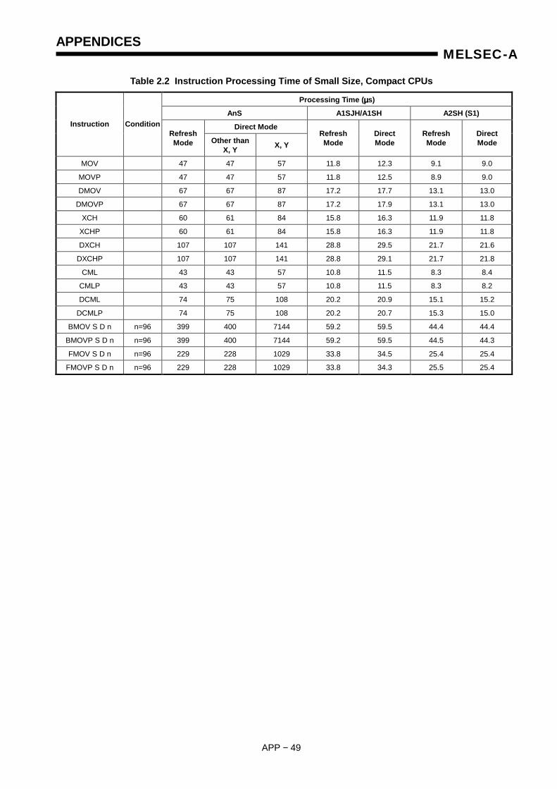
APPENDICES
APP − 49
MELSEC-A
Table 2.2 Instruction Processing Time of Small Size, Compact CPUs
Processing Time (µµµµs)
AnS A1SJH/A1SH A2SH (S1)
Direct Mode Instruction Condition Refresh Mode Other than
X, Y X, Y Refresh Mode
Direct Mode
Refresh Mode
Direct Mode
MOV 47 47 57 11.8 12.3 9.1 9.0
MOVP 47 47 57 11.8 12.5 8.9 9.0
DMOV 67 67 87 17.2 17.7 13.1 13.0
DMOVP 67 67 87 17.2 17.9 13.1 13.0
XCH 60 61 84 15.8 16.3 11.9 11.8
XCHP 60 61 84 15.8 16.3 11.9 11.8
DXCH 107 107 141 28.8 29.5 21.7 21.6
DXCHP 107 107 141 28.8 29.1 21.7 21.8
CML 43 43 57 10.8 11.5 8.3 8.4
CMLP 43 43 57 10.8 11.5 8.3 8.2
DCML 74 75 108 20.2 20.9 15.1 15.2
DCMLP 74 75 108 20.2 20.7 15.3 15.0
BMOV S D n n=96 399 400 7144 59.2 59.5 44.4 44.4
BMOVP S D n n=96 399 400 7144 59.2 59.5 44.5 44.3
FMOV S D n n=96 229 228 1029 33.8 34.5 25.4 25.4
FMOVP S D n n=96 229 228 1029 33.8 34.3 25.5 25.4
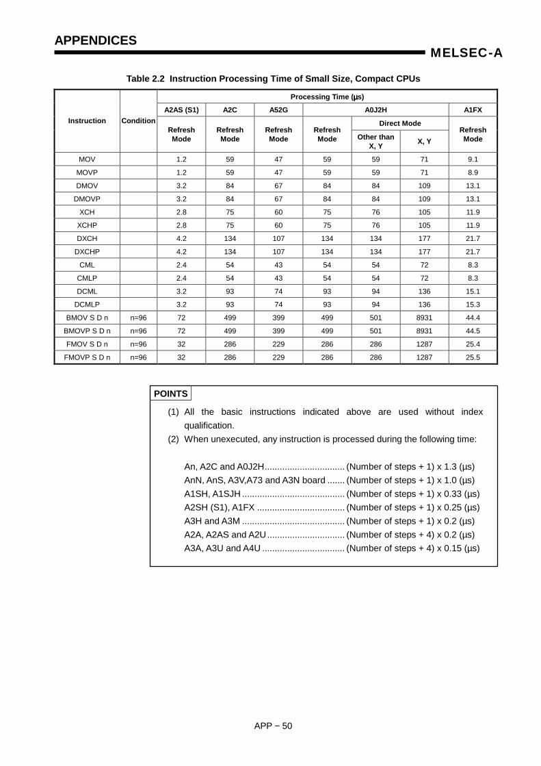
APPENDICES
APP − 50
MELSEC-A
Table 2.2 Instruction Processing Time of Small Size, Compact CPUs
Processing Time (µµµµs)
A2AS (S1) A2C A52G A0J2H A1FX
Direct Mode Instruction Condition Refresh Mode
Refresh Mode
Refresh Mode
Refresh Mode Other than
X, Y X, Y Refresh Mode
MOV 1.2 59 47 59 59 71 9.1
MOVP 1.2 59 47 59 59 71 8.9
DMOV 3.2 84 67 84 84 109 13.1
DMOVP 3.2 84 67 84 84 109 13.1
XCH 2.8 75 60 75 76 105 11.9
XCHP 2.8 75 60 75 76 105 11.9
DXCH 4.2 134 107 134 134 177 21.7
DXCHP 4.2 134 107 134 134 177 21.7
CML 2.4 54 43 54 54 72 8.3
CMLP 2.4 54 43 54 54 72 8.3
DCML 3.2 93 74 93 94 136 15.1
DCMLP 3.2 93 74 93 94 136 15.3
BMOV S D n n=96 72 499 399 499 501 8931 44.4
BMOVP S D n n=96 72 499 399 499 501 8931 44.5
FMOV S D n n=96 32 286 229 286 286 1287 25.4
FMOVP S D n n=96 32 286 229 286 286 1287 25.5
POINTS
(1) All the basic instructions indicated above are used without index qualification.
(2) When unexecuted, any instruction is processed during the following time: An, A2C and A0J2H................................ (Number of steps + 1) x 1.3 (µs) AnN, AnS, A3V,A73 and A3N board ....... (Number of steps + 1) x 1.0 (µs) A1SH, A1SJH ......................................... (Number of steps + 1) x 0.33 (µs) A2SH (S1), A1FX ................................... (Number of steps + 1) x 0.25 (µs) A3H and A3M ......................................... (Number of steps + 1) x 0.2 (µs) A2A, A2AS and A2U............................... (Number of steps + 4) x 0.2 (µs) A3A, A3U and A4U ................................. (Number of steps + 4) x 0.15 (µs)
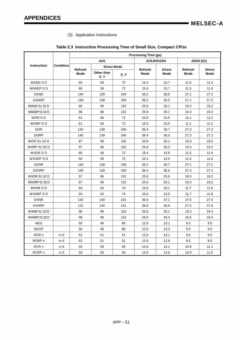
APPENDICES
APP − 51
MELSEC-A
(3) Application Instructions
Table 2.3 Instruction Processing Time of Small Size, Compact CPUs
Processing Time (µµµµs)
AnS A1SJH/A1SH A2SH (S1)
Direct Mode Instruction Condition Refresh Mode Other than
X, Y X, Y Refresh Mode
Direct Mode
Refresh Mode
Direct Mode
WAND S D 60 59 72 15.4 15.7 11.5 11.4
WANDP S D 60 59 72 15.4 15.7 11.5 11.6
DAND 140 139 240 36.2 36.5 27.1 27.2
DANDP 140 139 240 36.2 36.5 27.1 27.2
WAND S1 S2 D 96 96 152 25.8 26.1 19.3 19.2
WANDP S1 S2 D 96 96 152 25.8 26.1 19.3 19.2
WOR S D 61 60 72 15.0 15.5 11.1 11.2
WORP S D 61 60 72 15.0 15.5 11.1 11.2
DOR 140 139 240 36.4 36.7 27.3 27.2
DORP 140 139 240 36.4 36.9 27.3 27.2
WOR S1 S2 D 97 96 152 25.8 26.1 19.3 19.2
WORP S1 S2 D 97 96 152 25.8 26.3 19.3 19.2
WXOR S D 60 59 72 15.4 15.5 11.5 11.4
WXORP S D 60 59 72 15.4 15.5 11.5 11.6
DXOR 140 139 240 36.2 36.7 27.1 27.2
DXORP 140 139 240 36.4 36.5 27.3 27.2
WXOR S1 S2 D 97 96 152 25.6 25.9 19.3 19.2
WXORP S1 S2 D 97 96 152 25.6 26.1 19.3 19.2
WXNR S D 64 62 74 15.6 16.1 11.7 11.6
WXNRP S D 64 62 74 15.6 15.9 11.7 11.8
DXNR 142 140 241 36.6 37.1 27.5 27.4
DXNRP 142 140 241 36.6 36.9 27.5 27.6
WXNR S1 S2 D 98 96 152 25.6 26.1 19.3 19.4
WXNRP S1 S2 D 98 96 152 26.0 26.3 19.5 19.4
NEG 50 49 86 12.6 13.1 9.5 9.5
NEGP 50 49 86 12.6 13.3 9.5 9.5
ROR n n=3 52 51 51 12.6 13.1 9.5 9.5
RORP n n=3 52 51 51 12.6 12.9 9.5 9.5
RCR n n=3 59 59 59 14.6 15.1 10.9 11.1
RCRP n n=3 59 59 59 14.6 14.9 10.9 11.0
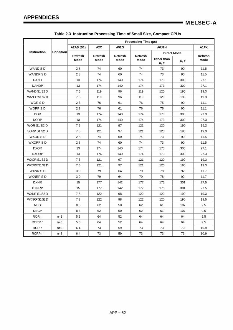
APPENDICES
APP − 52
MELSEC-A
Table 2.3 Instruction Processing Time of Small Size, Compact CPUs
Processing Time (µµµµs)
A2AS (S1) A2C A52G A0J2H A1FX
Direct Mode Instruction Condition Refresh Mode
Refresh Mode
Refresh Mode
Refresh Mode Other than
X, Y X, Y Refresh Mode
WAND S D 2.8 74 60 74 73 90 11.5
WANDP S D 2.8 74 60 74 73 90 11.5
DAND 13 174 140 174 173 300 27.1
DANDP 13 174 140 174 173 300 27.1
WAND S1 S2 D 7.6 119 96 119 120 190 19.3
WANDP S1 S2 D 7.6 119 96 119 120 190 19.3
WOR S D 2.8 76 61 76 75 90 11.1
WORP S D 2.8 76 61 76 75 90 11.1
DOR 13 174 140 174 173 300 27.3
DORP 13 174 140 174 173 300 27.3
WOR S1 S2 D 7.6 121 97 121 120 190 19.3
SORP S1 S2 D 7.6 121 97 121 120 190 19.3
WXOR S D 2.8 74 60 74 73 90 11.5
WXORP S D 2.8 74 60 74 73 90 11.5
DXOR 13 174 140 174 173 300 27.1
DXORP 13 174 140 174 173 300 27.3
WXOR S1 S2 D 7.6 121 97 121 120 190 19.3
WXORP S1 S2 D 7.6 121 97 121 120 190 19.3
WXNR S D 3.0 79 64 79 78 92 11.7
WXNRP S D 3.0 79 64 79 78 92 11.7
DXNR 15 177 142 177 175 301 27.5
DXNRP 15 177 142 177 175 301 27.5
WXNR S1 S2 D 7.8 122 98 122 120 190 19.3
WXNRP S1 S2 D 7.8 122 98 122 120 190 19.5
NEG 8.6 62 50 62 61 107 9.5
NEGP 8.6 62 50 62 61 107 9.5
ROR n n=3 5.8 64 52 64 64 64 9.5
RORP n n=3 5.8 64 52 64 64 64 9.5
RCR n n=3 6.4 73 59 73 73 73 10.9
RCRP n n=3 6.4 73 59 73 73 73 10.9
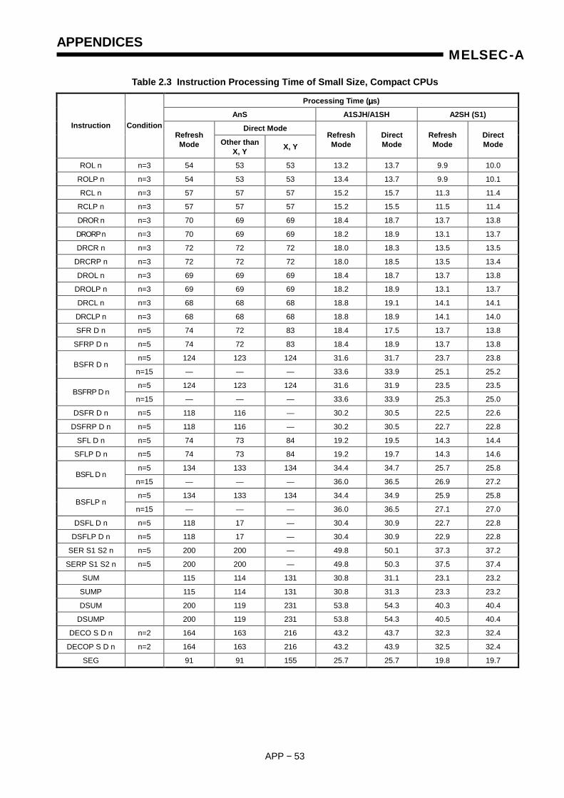
APPENDICES
APP − 53
MELSEC-A
Table 2.3 Instruction Processing Time of Small Size, Compact CPUs
Processing Time (µµµµs)
AnS A1SJH/A1SH A2SH (S1)
Direct Mode Instruction Condition Refresh Mode Other than
X, Y X, Y Refresh Mode
Direct Mode
Refresh Mode
Direct Mode
ROL n n=3 54 53 53 13.2 13.7 9.9 10.0
ROLP n n=3 54 53 53 13.4 13.7 9.9 10.1
RCL n n=3 57 57 57 15.2 15.7 11.3 11.4
RCLP n n=3 57 57 57 15.2 15.5 11.5 11.4
DROR n n=3 70 69 69 18.4 18.7 13.7 13.8
DRORP n n=3 70 69 69 18.2 18.9 13.1 13.7
DRCR n n=3 72 72 72 18.0 18.3 13.5 13.5
DRCRP n n=3 72 72 72 18.0 18.5 13.5 13.4
DROL n n=3 69 69 69 18.4 18.7 13.7 13.8
DROLP n n=3 69 69 69 18.2 18.9 13.1 13.7
DRCL n n=3 68 68 68 18.8 19.1 14.1 14.1
DRCLP n n=3 68 68 68 18.8 18.9 14.1 14.0
SFR D n n=5 74 72 83 18.4 17.5 13.7 13.8
SFRP D n n=5 74 72 83 18.4 18.9 13.7 13.8
n=5 124 123 124 31.6 31.7 23.7 23.8 BSFR D n
n=15 — — — 33.6 33.9 25.1 25.2
n=5 124 123 124 31.6 31.9 23.5 23.5 BSFRP D n
n=15 — — — 33.6 33.9 25.3 25.0
DSFR D n n=5 118 116 — 30.2 30.5 22.5 22.6
DSFRP D n n=5 118 116 — 30.2 30.5 22.7 22.8
SFL D n n=5 74 73 84 19.2 19.5 14.3 14.4
SFLP D n n=5 74 73 84 19.2 19.7 14.3 14.6
n=5 134 133 134 34.4 34.7 25.7 25.8 BSFL D n
n=15 — — — 36.0 36.5 26.9 27.2
n=5 134 133 134 34.4 34.9 25.9 25.8 BSFLP n
n=15 — — — 36.0 36.5 27.1 27.0
DSFL D n n=5 118 17 — 30.4 30.9 22.7 22.8
DSFLP D n n=5 118 17 — 30.4 30.9 22.9 22.8
SER S1 S2 n n=5 200 200 — 49.8 50.1 37.3 37.2
SERP S1 S2 n n=5 200 200 — 49.8 50.3 37.5 37.4
SUM 115 114 131 30.8 31.1 23.1 23.2
SUMP 115 114 131 30.8 31.3 23.3 23.2
DSUM 200 119 231 53.8 54.3 40.3 40.4
DSUMP 200 119 231 53.8 54.3 40.5 40.4
DECO S D n n=2 164 163 216 43.2 43.7 32.3 32.4
DECOP S D n n=2 164 163 216 43.2 43.9 32.5 32.4
SEG 91 91 155 25.7 25.7 19.8 19.7

APPENDICES
APP − 54
MELSEC-A
Table 2.3 Instruction Processing Time of Small Size, Compact CPUs
Processing Time (µµµµs)
A2AS (S1) A2C A52G A0J2H A1FX
Direct Mode Instruction Condition Refresh Mode
Refresh Mode
Refresh Mode
Refresh Mode Other than
X, Y X, Y Refresh Mode
ROL n n=3 11 67 54 67 67 67 9.9
ROLP n n=3 11 67 54 67 67 67 9.9
RCL n n=3 12 71 57 71 71 71 11.3
RCLP n n=3 12 71 57 71 71 71 11.5
DROR n n=3 5.8 87 70 87 87 87 13.7
DRORP n n=3 5.8 87 70 87 87 87 13.7
DRCR n n=3 6.4 89 72 89 90 90 13.5
DRCRP n n=3 6.4 89 72 89 90 90 13.5
DROL n n=3 10 87 70 87 87 87 13.7
DROLP n n=3 10 87 70 87 87 87 13.1
DRCL n n=3 12 84 68 84 85 85 14.1
DRCLP n n=3 12 84 68 84 85 85 14.1
SFR D n n=5 5.0 92 74 92 90 103 13.7
SFRP D n n=5 5.0 92 74 92 90 103 13.7
n=5 29 154 124 154 153 155 23.7 BSFR D n
n=15 — — — — — — 25.1
n=5 29 154 124 154 153 155 23.5 BSFRP D n
n=15 — — — — — — 25.3
DSFR D n n=5 18.8 147 118 147 145 — 22.5
DSFRP D n n=5 18.8 147 118 147 145 — 22.7
SFL D n n=5 4.8 92 74 92 91 105 14.3
SFLP D n n=5 4.8 92 74 92 91 105 14.3
n=5 28 167 134 167 166 167 25.7 BSFL D n
n=15 — — — — — — 26.9
n=5 28 167 134 167 166 167 25.9 BSFLP n
n=15 — — — — — — 27.1
DSFL D n n=5 22 147 118 147 146 — 22.7
DSFLP D n n=5 22 147 118 147 146 — 22.9
SER S1 S2 n n=5 33 249 200 249 250 — 37.3
SERP S1 S2 n n=5 33 249 200 249 250 — 37.5
SUM 15 143 115 143 143 163 23.1
SUMP 15 143 115 143 143 163 23.3
DSUM 34 249 200 249 248 288 40.3
DSUMP 34 249 200 248 249 288 40.5
DECO S D n n=2 28 204 164 204 203 270 32.3
DECOP S D n n=2 28 204 164 204 203 270 32.5
SEG 6.4 800 91 113 113 193 19.8
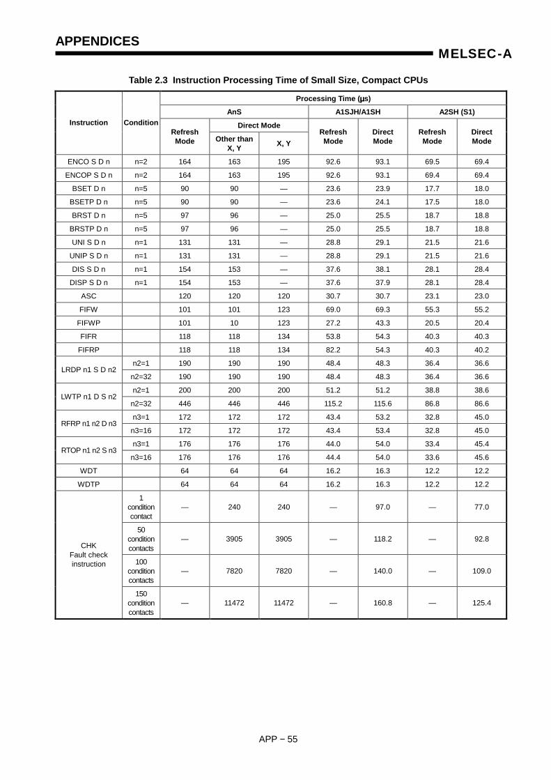
APPENDICES
APP − 55
MELSEC-A
Table 2.3 Instruction Processing Time of Small Size, Compact CPUs
Processing Time (µµµµs)
AnS A1SJH/A1SH A2SH (S1)
Direct Mode Instruction Condition Refresh Mode Other than
X, Y X, Y Refresh Mode
Direct Mode
Refresh Mode
Direct Mode
ENCO S D n n=2 164 163 195 92.6 93.1 69.5 69.4
ENCOP S D n n=2 164 163 195 92.6 93.1 69.4 69.4
BSET D n n=5 90 90 — 23.6 23.9 17.7 18.0
BSETP D n n=5 90 90 — 23.6 24.1 17.5 18.0
BRST D n n=5 97 96 — 25.0 25.5 18.7 18.8
BRSTP D n n=5 97 96 — 25.0 25.5 18.7 18.8
UNI S D n n=1 131 131 — 28.8 29.1 21.5 21.6
UNIP S D n n=1 131 131 — 28.8 29.1 21.5 21.6
DIS S D n n=1 154 153 — 37.6 38.1 28.1 28.4
DISP S D n n=1 154 153 — 37.6 37.9 28.1 28.4
ASC 120 120 120 30.7 30.7 23.1 23.0
FIFW 101 101 123 69.0 69.3 55.3 55.2
FIFWP 101 10 123 27.2 43.3 20.5 20.4
FIFR 118 118 134 53.8 54.3 40.3 40.3
FIFRP 118 118 134 82.2 54.3 40.3 40.2
n2=1 190 190 190 48.4 48.3 36.4 36.6 LRDP n1 S D n2
n2=32 190 190 190 48.4 48.3 36.4 36.6
n2=1 200 200 200 51.2 51.2 38.8 38.6 LWTP n1 D S n2
n2=32 446 446 446 115.2 115.6 86.8 86.6
n3=1 172 172 172 43.4 53.2 32.8 45.0 RFRP n1 n2 D n3
n3=16 172 172 172 43.4 53.4 32.8 45.0
n3=1 176 176 176 44.0 54.0 33.4 45.4 RTOP n1 n2 S n3
n3=16 176 176 176 44.4 54.0 33.6 45.6
WDT 64 64 64 16.2 16.3 12.2 12.2
WDTP 64 64 64 16.2 16.3 12.2 12.2
1 condition contact
— 240 240 — 97.0 — 77.0
50 condition contacts
— 3905 3905 — 118.2 — 92.8
100 condition contacts
— 7820 7820 — 140.0 — 109.0
CHK Fault check instruction
150 condition contacts
— 11472 11472 — 160.8 — 125.4
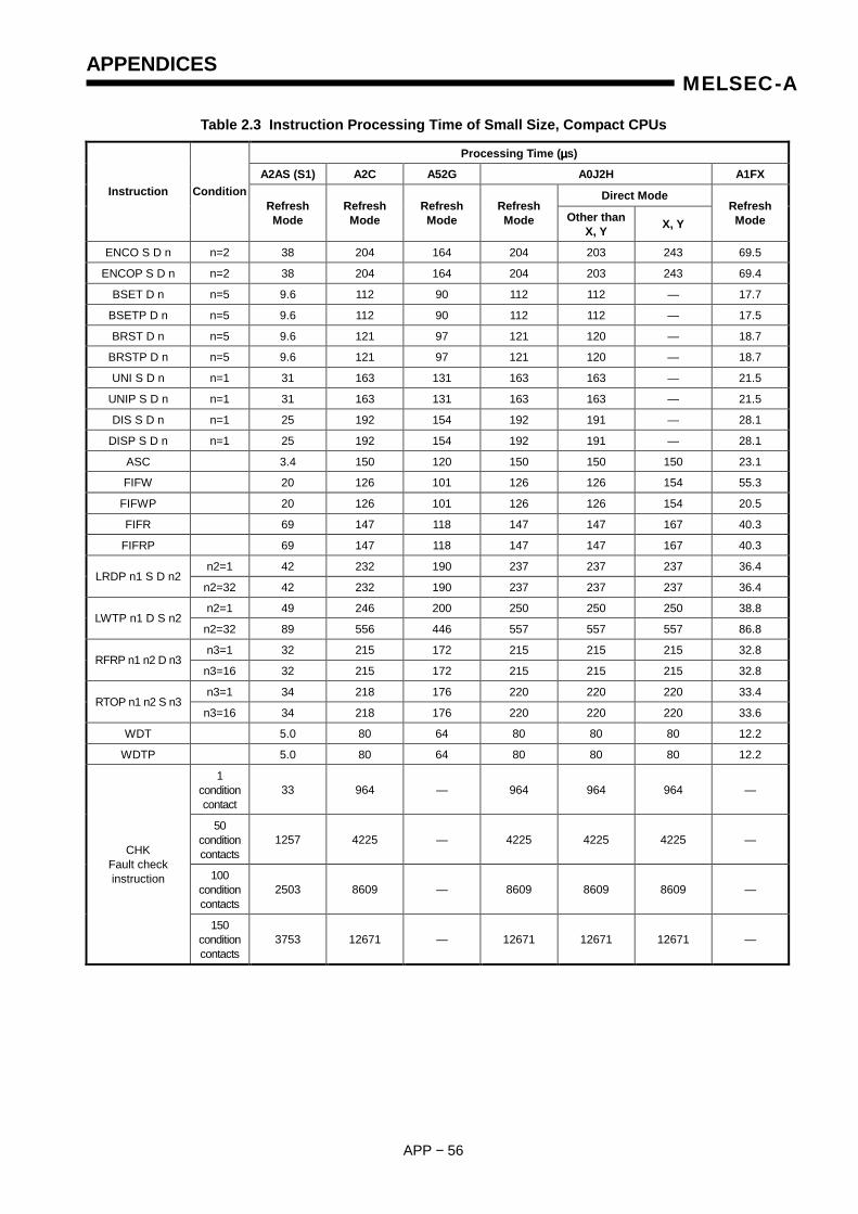
APPENDICES
APP − 56
MELSEC-A
Table 2.3 Instruction Processing Time of Small Size, Compact CPUs
Processing Time (µµµµs)
A2AS (S1) A2C A52G A0J2H A1FX
Direct Mode Instruction Condition Refresh Mode
Refresh Mode
Refresh Mode
Refresh Mode Other than
X, Y X, Y Refresh Mode
ENCO S D n n=2 38 204 164 204 203 243 69.5
ENCOP S D n n=2 38 204 164 204 203 243 69.4
BSET D n n=5 9.6 112 90 112 112 — 17.7
BSETP D n n=5 9.6 112 90 112 112 — 17.5
BRST D n n=5 9.6 121 97 121 120 — 18.7
BRSTP D n n=5 9.6 121 97 121 120 — 18.7
UNI S D n n=1 31 163 131 163 163 — 21.5
UNIP S D n n=1 31 163 131 163 163 — 21.5
DIS S D n n=1 25 192 154 192 191 — 28.1
DISP S D n n=1 25 192 154 192 191 — 28.1
ASC 3.4 150 120 150 150 150 23.1
FIFW 20 126 101 126 126 154 55.3
FIFWP 20 126 101 126 126 154 20.5
FIFR 69 147 118 147 147 167 40.3
FIFRP 69 147 118 147 147 167 40.3
n2=1 42 232 190 237 237 237 36.4 LRDP n1 S D n2
n2=32 42 232 190 237 237 237 36.4
n2=1 49 246 200 250 250 250 38.8 LWTP n1 D S n2
n2=32 89 556 446 557 557 557 86.8
n3=1 32 215 172 215 215 215 32.8 RFRP n1 n2 D n3
n3=16 32 215 172 215 215 215 32.8
n3=1 34 218 176 220 220 220 33.4 RTOP n1 n2 S n3
n3=16 34 218 176 220 220 220 33.6
WDT 5.0 80 64 80 80 80 12.2
WDTP 5.0 80 64 80 80 80 12.2
1 condition contact
33 964 — 964 964 964 —
50 condition contacts
1257 4225 — 4225 4225 4225 —
100 condition contacts
2503 8609 — 8609 8609 8609 —
CHK Fault check instruction
150 condition contacts
3753 12671 — 12671 12671 12671 —
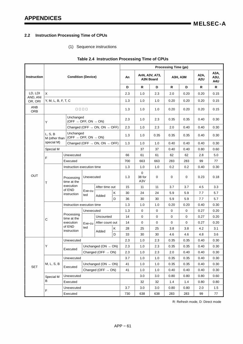
APPENDICES
APP − 61
MELSEC-A
2.2 Instruction Processing Time of CPUs
(1) Sequence instructions Table 2.4 Instruction Processing Time of CPUs
Processing Time (µµµµs)
An AnN, A3V, A73, A3N Board A3H, A3M A2A,
A2U
A3A, A3U, A4U
Instruction Condition (Device)
D R D R D R R
X 2.3 1.0 2.3 2.0 0.20 0.20 0.15 LD, LDI AND, ANI OR, ORI Y, M, L, B, F, T, C 1.3 1.0 1.0 0.20 0.20 0.20 0.15
ANB ORB 1.3 1.0 1.0 0.20 0.20 0.20 0.15
Unchanged (OFF → OFF, ON → ON) 2.3 1.0 2.3 0.35 0.35 0.40 0.30
Y Changed (OFF → ON, ON → OFF) 2.3 1.0 2.3 2.0 0.40 0.40 0.30
Unchanged (OFF → OFF, ON → ON) 1.3 1.0 0.35 0.35 0.35 0.40 0.30 L, S, B
M (other than special M) Changed (OFF → ON, ON → OFF) 1.3 1.0 1.0 0.40 0.40 0.40 0.30
Special M 37 37 0.40 0.40 0.80 0.60
Unexecuted 66 61 61 62 62 2.8 5.0 F
Executed 700 663 663 283 283 99 77
Instruction execution time 1.3 1.0 1.0 0.2 0.2 0.40 0.30
Unexecuted 1.3 0
38 for A3V
0 0 0 0.23 0.18
After time out 15 11 11 3.7 3.7 4.5 3.3
K 30 24 24 5.9 5.9 7.7 5.7
T Processing time at the execution of END instruction
Exe-cuted Added
D 36 30 30 5.9 5.9 7.7 5.7
Instruction execution time 1.3 1.0 1.0 0.20 0.20 0.40 0.30
Unexecuted 1.3 0 0 0 0 0.27 0.20
Uncounted 14 0 0 0 0 0.27 0.20
After count out 14 0 0 0 0 0.27 0.20
K 28 25 25 3.8 3.8 4.2 3.1
OUT
C Processing time at the execution of END instruction
Exe-cuted
Added D 33 30 30 4.6 4.6 4.8 3.6
Unexecuted 2.3 1.0 2.3 0.35 0.35 0.40 0.30
Unchanged (ON → ON) 2.3 1.0 2.3 0.35 0.35 0.40 0.30 Y Executed
Changed (OFF → ON) 2.3 1.0 2.3 2.0 0.40 0.40 0.30
Unexecuted 3.7 1.0 1.0 0.35 0.35 0.40 0.30
Unchanged (ON → ON) 41 1.0 1.0 0.35 0.35 0.40 0.30 M, L, S, B Executed
Changed (OFF → ON) 41 1.0 1.0 0.40 0.40 0.40 0.30
Unexecuted 3.0 3.0 0.80 0.80 0.80 0.60 Special M B Executed 32 32 1.4 1.4 0.80 0.80
Unexecuted 3.7 3.0 3.0 0.80 0.80 2.0 1.5
SET
F Executed 730 638 638 283 283 99 77
R: Refresh mode, D: Direct mode
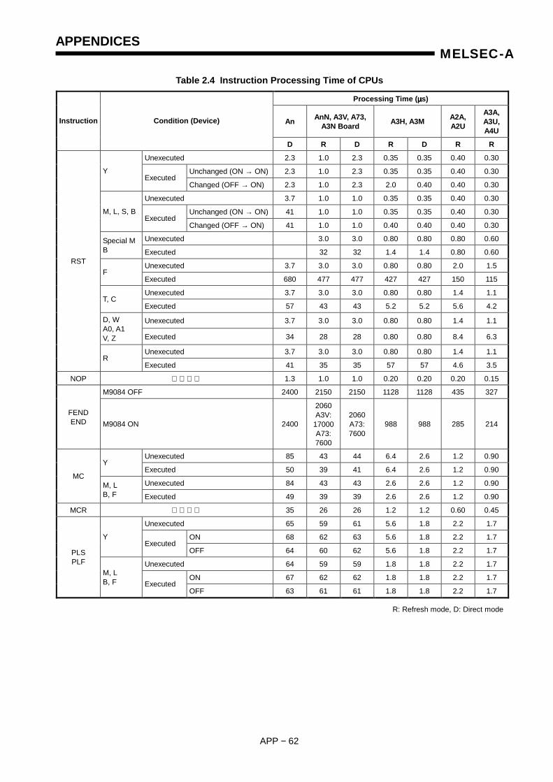
APPENDICES
APP − 62
MELSEC-A
Table 2.4 Instruction Processing Time of CPUs
Processing Time (µµµµs)
An AnN, A3V, A73, A3N Board A3H, A3M A2A,
A2U
A3A, A3U, A4U
Instruction Condition (Device)
D R D R D R R
Unexecuted 2.3 1.0 2.3 0.35 0.35 0.40 0.30
Unchanged (ON → ON) 2.3 1.0 2.3 0.35 0.35 0.40 0.30 Y Executed
Changed (OFF → ON) 2.3 1.0 2.3 2.0 0.40 0.40 0.30
Unexecuted 3.7 1.0 1.0 0.35 0.35 0.40 0.30
Unchanged (ON → ON) 41 1.0 1.0 0.35 0.35 0.40 0.30 M, L, S, B Executed
Changed (OFF → ON) 41 1.0 1.0 0.40 0.40 0.40 0.30
Unexecuted 3.0 3.0 0.80 0.80 0.80 0.60 Special M B Executed 32 32 1.4 1.4 0.80 0.60
Unexecuted 3.7 3.0 3.0 0.80 0.80 2.0 1.5 F
Executed 680 477 477 427 427 150 115
Unexecuted 3.7 3.0 3.0 0.80 0.80 1.4 1.1 T, C
Executed 57 43 43 5.2 5.2 5.6 4.2
Unexecuted 3.7 3.0 3.0 0.80 0.80 1.4 1.1 D, W A0, A1 V, Z Executed 34 28 28 0.80 0.80 8.4 6.3
Unexecuted 3.7 3.0 3.0 0.80 0.80 1.4 1.1
RST
R Executed 41 35 35 57 57 4.6 3.5
NOP 1.3 1.0 1.0 0.20 0.20 0.20 0.15
M9084 OFF 2400 2150 2150 1128 1128 435 327
FEND END M9084 ON 2400
2060 A3V:
17000A73: 7600
2060 A73: 7600
988 988 285 214
Unexecuted 85 43 44 6.4 2.6 1.2 0.90 Y
Executed 50 39 41 6.4 2.6 1.2 0.90
Unexecuted 84 43 43 2.6 2.6 1.2 0.90 MC
M, L B, F Executed 49 39 39 2.6 2.6 1.2 0.90
MCR 35 26 26 1.2 1.2 0.60 0.45
Unexecuted 65 59 61 5.6 1.8 2.2 1.7
ON 68 62 63 5.6 1.8 2.2 1.7 Y Executed
OFF 64 60 62 5.6 1.8 2.2 1.7
Unexecuted 64 59 59 1.8 1.8 2.2 1.7
ON 67 62 62 1.8 1.8 2.2 1.7
PLS PLF
M, L B, F Executed
OFF 63 61 61 1.8 1.8 2.2 1.7
R: Refresh mode, D: Direct mode
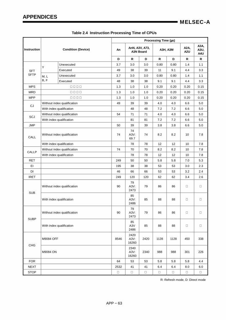
APPENDICES
APP − 63
MELSEC-A
Table 2.4 Instruction Processing Time of CPUs
Processing Time (µµµµs)
An AnN, A3V, A73, A3N Board A3H, A3M A2A,
A2U
A3A, A3U, A4U
Instruction Condition (Device)
D R D R D R R
Unexecuted 3.7 3.0 3.0 0.80 0.80 1.4 1.1 Y
Executed 49 38 39 11 9.1 4.4 3.3
Unexecuted 3.7 3.0 3.0 0.80 0.80 1.4 1.1 SFT
SFTP M, L B, F Executed 48 38 38 9.1 9.1 4.4 3.3
MPS 1.3 1.0 1.0 0.20 0.20 0.20 0.15
MRD 1.3 1.0 1.0 0.20 0.20 0.20 0.15
MPP 1.3 1.0 1.0 0.20 0.20 0.20 0.15
Without index qualification 49 39 39 4.0 4.0 6.6 5.0 CJ
With index qualification 48 48 7.2 7.2 6.6 5.0
Without index qualification 54 71 71 4.0 4.0 6.6 5.0 SCJ
With index qualification 81 81 7.2 7.2 6.6 5.0
JMP 50 39 39 3.8 3.8 6.6 5.0
Without index qualification 74 74
A3V: 69.7
74 8.2 8.2 10 7.8 CALL
With index qualification 78 78 12 12 10 7.8
Without index qualification 74 70 70 8.2 8.2 10 7.8 CALLP
With index qualification 78 78 12 12 10 7.8
RET 249 50 50 5.8 5.8 7.0 5.3
EI 195 38 38 53 53 3.0 2.3
DI 46 66 66 53 53 3.2 2.4
IRET 249 120 120 62 62 3.4 2.6
Without index qualification 90 79
A3V: 2473
79 86 86
SUB
With index qualification 85
A3V: 2486
85 88 88
Without index qualification 90 79
A3V: 2473
79 86 86
SUBP
With index qualification 85
A3V 2486
85 88 88
M9084 OFF 8546 2420 A3V:
16260 2420 1128 1128 450 338
CHG
M9084 ON 2340 A3V:
16260 2340 988 988 301 226
FOR 64 53 53 5.8 5.8 5.8 4.4
NEXT 2532 41 41 6.4 6.4 8.0 6.0
STOP
R: Refresh mode, D: Direct mode
APPENDICES
APP − 64
MELSEC-A
POINTS
(1) "When not executed" in the above table indicates that the input condition is off.
(2) "When not counted" of OUT C instruction indicates that the input condition
remains on and the counter does not count.
(3) "OFF" of PLS and PLF instructions indicates that the input condition remains on 1 scan after it has turned on (off for PLF), and the pulse is not generated.
(4) T/C count processing time and refresh time are not included in the FEND, END, CHG instruction processing times.
Input condition
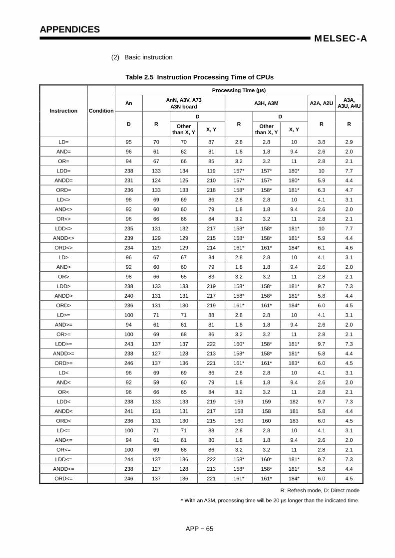
APPENDICES
APP − 65
MELSEC-A
(2) Basic instruction Table 2.5 Instruction Processing Time of CPUs
Processing Time (µµµµs)
An AnN, A3V, A73 A3N board A3H, A3M A2A, A2U A3A,
A3U, A4U
D D Instruction Condition
D R Other than X, Y X, Y
R Other than X, Y X, Y
R R
LD= 95 70 70 87 2.8 2.8 10 3.8 2.9
AND= 96 61 62 81 1.8 1.8 9.4 2.6 2.0
OR= 94 67 66 85 3.2 3.2 11 2.8 2.1
LDD= 238 133 134 119 157* 157* 180* 10 7.7
ANDD= 231 124 125 210 157* 157* 180* 5.9 4.4
ORD= 236 133 133 218 158* 158* 181* 6.3 4.7
LD<> 98 69 69 86 2.8 2.8 10 4.1 3.1
AND<> 92 60 60 79 1.8 1.8 9.4 2.6 2.0
OR<> 96 66 66 84 3.2 3.2 11 2.8 2.1
LDD<> 235 131 132 217 158* 158* 181* 10 7.7
ANDD<> 239 129 129 215 158* 158* 181* 5.9 4.4
ORD<> 234 129 129 214 161* 161* 184* 6.1 4.6
LD> 96 67 67 84 2.8 2.8 10 4.1 3.1
AND> 92 60 60 79 1.8 1.8 9.4 2.6 2.0
OR> 98 66 65 83 3.2 3.2 11 2.8 2.1
LDD> 238 133 133 219 158* 158* 181* 9.7 7.3
ANDD> 240 131 131 217 158* 158* 181* 5.8 4.4
ORD> 236 131 130 219 161* 161* 184* 6.0 4.5
LD>= 100 71 71 88 2.8 2.8 10 4.1 3.1
AND>= 94 61 61 81 1.8 1.8 9.4 2.6 2.0
OR>= 100 69 68 86 3.2 3.2 11 2.8 2.1
LDD>= 243 137 137 222 160* 158* 181* 9.7 7.3
ANDD>= 238 127 128 213 158* 158* 181* 5.8 4.4
ORD>= 246 137 136 221 161* 161* 183* 6.0 4.5
LD< 96 69 69 86 2.8 2.8 10 4.1 3.1
AND< 92 59 60 79 1.8 1.8 9.4 2.6 2.0
OR< 96 66 65 84 3.2 3.2 11 2.8 2.1
LDD< 238 133 133 219 159 159 182 9.7 7.3
ANDD< 241 131 131 217 158 158 181 5.8 4.4
ORD< 236 131 130 215 160 160 183 6.0 4.5
LD<= 100 71 71 88 2.8 2.8 10 4.1 3.1
AND<= 94 61 61 80 1.8 1.8 9.4 2.6 2.0
OR<= 100 69 68 86 3.2 3.2 11 2.8 2.1
LDD<= 244 137 136 222 158* 160* 181* 9.7 7.3
ANDD<= 238 127 128 213 158* 158* 181* 5.8 4.4
ORD<= 246 137 136 221 161* 161* 184* 6.0 4.5
R: Refresh mode, D: Direct mode
* With an A3M, processing time will be 20 µs longer than the indicated time.
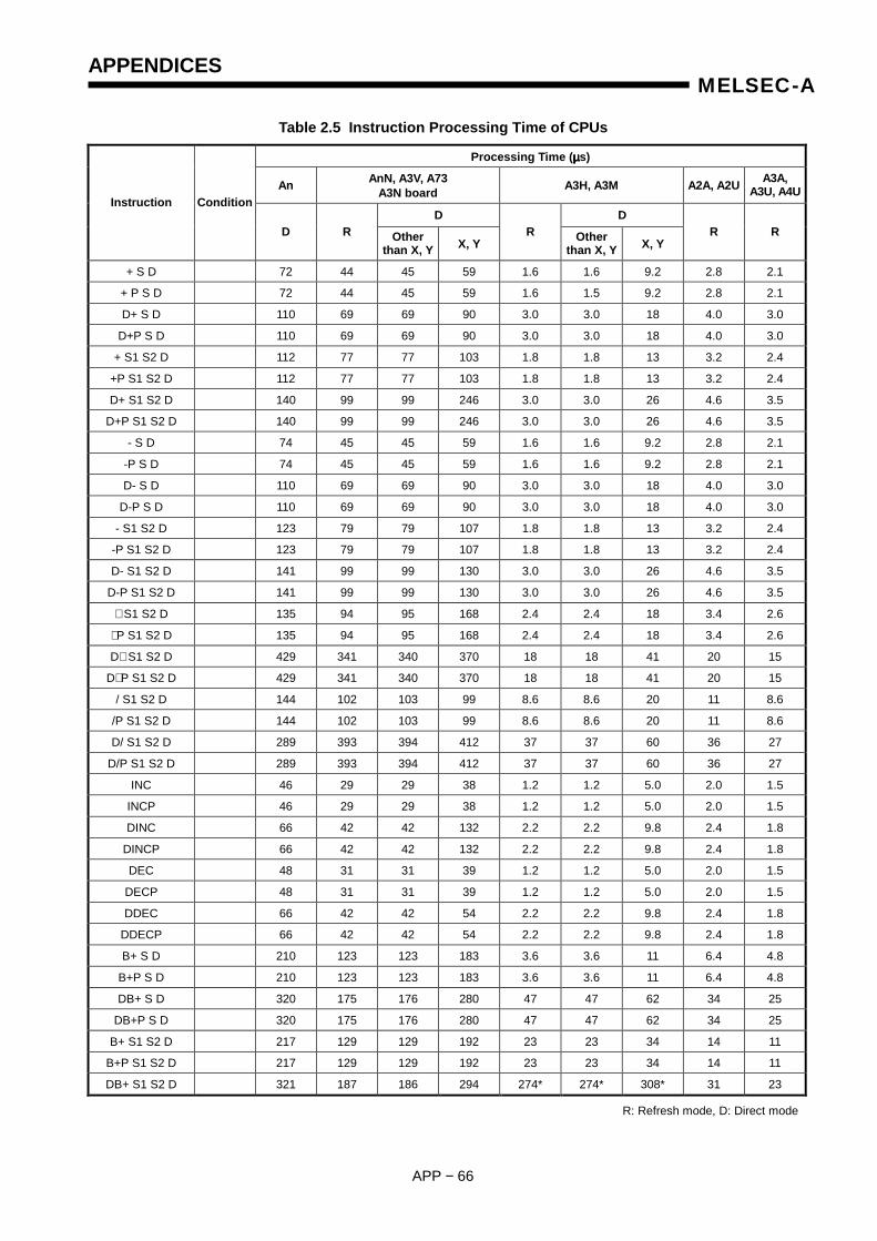
APPENDICES
APP − 66
MELSEC-A
Table 2.5 Instruction Processing Time of CPUs
Processing Time (µµµµs)
An AnN, A3V, A73 A3N board A3H, A3M A2A, A2U A3A,
A3U, A4U
D D Instruction Condition
D R Other than X, Y X, Y
R Other than X, Y X, Y
R R
+ S D 72 44 45 59 1.6 1.6 9.2 2.8 2.1
+ P S D 72 44 45 59 1.6 1.5 9.2 2.8 2.1
D+ S D 110 69 69 90 3.0 3.0 18 4.0 3.0
D+P S D 110 69 69 90 3.0 3.0 18 4.0 3.0
+ S1 S2 D 112 77 77 103 1.8 1.8 13 3.2 2.4
+P S1 S2 D 112 77 77 103 1.8 1.8 13 3.2 2.4
D+ S1 S2 D 140 99 99 246 3.0 3.0 26 4.6 3.5
D+P S1 S2 D 140 99 99 246 3.0 3.0 26 4.6 3.5
- S D 74 45 45 59 1.6 1.6 9.2 2.8 2.1
-P S D 74 45 45 59 1.6 1.6 9.2 2.8 2.1
D- S D 110 69 69 90 3.0 3.0 18 4.0 3.0
D-P S D 110 69 69 90 3.0 3.0 18 4.0 3.0
- S1 S2 D 123 79 79 107 1.8 1.8 13 3.2 2.4
-P S1 S2 D 123 79 79 107 1.8 1.8 13 3.2 2.4
D- S1 S2 D 141 99 99 130 3.0 3.0 26 4.6 3.5
D-P S1 S2 D 141 99 99 130 3.0 3.0 26 4.6 3.5
∗ S1 S2 D 135 94 95 168 2.4 2.4 18 3.4 2.6
∗ P S1 S2 D 135 94 95 168 2.4 2.4 18 3.4 2.6
D∗ S1 S2 D 429 341 340 370 18 18 41 20 15
D∗ P S1 S2 D 429 341 340 370 18 18 41 20 15
/ S1 S2 D 144 102 103 99 8.6 8.6 20 11 8.6
/P S1 S2 D 144 102 103 99 8.6 8.6 20 11 8.6
D/ S1 S2 D 289 393 394 412 37 37 60 36 27
D/P S1 S2 D 289 393 394 412 37 37 60 36 27
INC 46 29 29 38 1.2 1.2 5.0 2.0 1.5
INCP 46 29 29 38 1.2 1.2 5.0 2.0 1.5
DINC 66 42 42 132 2.2 2.2 9.8 2.4 1.8
DINCP 66 42 42 132 2.2 2.2 9.8 2.4 1.8
DEC 48 31 31 39 1.2 1.2 5.0 2.0 1.5
DECP 48 31 31 39 1.2 1.2 5.0 2.0 1.5
DDEC 66 42 42 54 2.2 2.2 9.8 2.4 1.8
DDECP 66 42 42 54 2.2 2.2 9.8 2.4 1.8
B+ S D 210 123 123 183 3.6 3.6 11 6.4 4.8
B+P S D 210 123 123 183 3.6 3.6 11 6.4 4.8
DB+ S D 320 175 176 280 47 47 62 34 25
DB+P S D 320 175 176 280 47 47 62 34 25
B+ S1 S2 D 217 129 129 192 23 23 34 14 11
B+P S1 S2 D 217 129 129 192 23 23 34 14 11
DB+ S1 S2 D 321 187 186 294 274* 274* 308* 31 23
R: Refresh mode, D: Direct mode
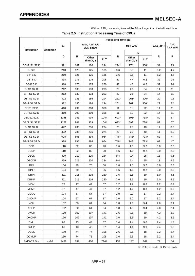
APPENDICES
APP − 67
MELSEC-A
* With an A3M, processing time will be 20 µs longer than the indicated time.
Table 2.5 Instruction Processing Time of CPUs
Processing Time (µµµµs)
An AnN, A3V, A73 A3N board A3H, A3M A2A, A2U A3A,
A3U, A4U
D D Instruction Condition
D R Other than X, Y X, Y
R Other than X, Y X, Y
R R
DB+P S1 S2 D 321 187 186 294 274* 274* 308* 31 23
B- S D 210 125 125 185 3.6 3.6 11 6.2 4.7
B-P S D 210 125 125 185 3.6 3.6 11 6.2 4.7
DB- S D 318 175 175 208 47 47 6.2 32 24
DB-P S D 318 175 175 280 47 47 6.2 32 24
B- S1 S2 D 212 133 133 203 23 23 34 14 11
B-P S1 S2 D 212 133 133 203 23 23 34 14 11
DB- S1 S2 D 322 185 186 294 261* 261* 306* 29 22
DB-P S1 S2 D 322 185 186 294 261* 261* 306* 29 22
B∗ S1 S2 D 410 299 300 358 11 11 22 14 11
B∗ P S1 S2 D 410 299 300 358 11 11 22 14 11
DB∗ S1 S2 D 1158 941 939 1044 693* 693* 738* 89 67
DB∗ P S1 S2 D 1158 941 939 1044 693* 693* 738* 89 67
B/ S1 S2 D 422 235 236 274 25 25 40 11 8.0
B/P S1 S2 D 422 235 236 274 25 25 40 11 8.0
DB/ S1 S2 D 998 896 894 954 748* 748* 793* 62 47
DB/P S1 S2 D 998 896 894 954 748* 748* 793* 62 47
BCD 110 82 83 90 1.6 1.6 9.2 3.0 2.3
BCDP 110 82 83 90 1.6 1.6 9.2 3.0 2.3
DBCD 329 219 220 284 9.4 9.4 25 13 9.5
DBCDP 329 219 220 284 9.4 9.4 25 13 9.5
BIN 104 79 78 86 1.6 1.6 9.2 3.0 2.3
BINP 104 79 78 86 1.6 1.6 9.2 3.0 2.3
DBIN 311 215 216 280 3.6 3.6 19 6.0 4.5
DBINP 311 215 216 280 3.6 3.6 19 6.0 4.5
MOV 72 47 47 57 1.2 1.2 8.8 1.2 0.9
MOVP 72 47 47 57 1.2 1.2 8.8 1.2 0.9
DMOV 104 67 67 87 2.0 2.0 17 3.2 2.4
DMOVP 104 67 67 87 2.0 2.0 17 3.2 2.4
XCH 102 60 61 84 1.8 1.8 9.4 2.8 2.1
XCHP 102 60 61 84 1.8 1.8 9.4 2.8 2.1
DXCH 170 107 107 141 3.6 3.6 19 4.2 3.2
DXCHP 170 107 107 141 3.6 3.6 19 4.2 3.2
CML 68 43 43 57 1.4 1.4 9.0 2.4 1.8
CMLP 68 43 43 57 1.4 1.4 9.0 2.4 1.8
DCML 130 74 74 108 2.6 2.6 18 3.2 2.4
DCMLP 130 74 75 108 2.6 2.6 18 3.2 2.4
BMOV S D n n=96 7498 699 400 7144 132 132 862 72 54
R: Refresh mode, D: Direct mode
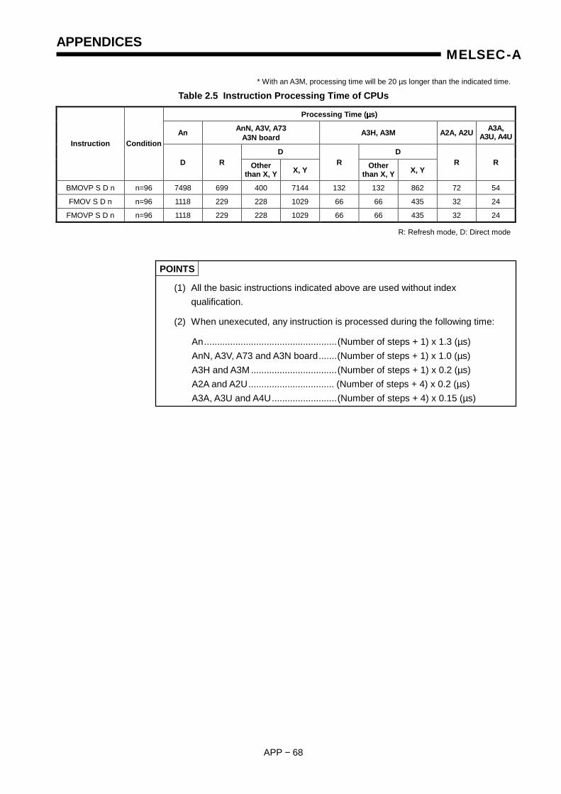
APPENDICES
APP − 68
MELSEC-A
* With an A3M, processing time will be 20 µs longer than the indicated time. Table 2.5 Instruction Processing Time of CPUs
Processing Time (µµµµs)
An AnN, A3V, A73 A3N board A3H, A3M A2A, A2U A3A,
A3U, A4U
D D Instruction Condition
D R Other than X, Y X, Y
R Other than X, Y X, Y
R R
BMOVP S D n n=96 7498 699 400 7144 132 132 862 72 54
FMOV S D n n=96 1118 229 228 1029 66 66 435 32 24
FMOVP S D n n=96 1118 229 228 1029 66 66 435 32 24
R: Refresh mode, D: Direct mode
POINTS
(1) All the basic instructions indicated above are used without index qualification.
(2) When unexecuted, any instruction is processed during the following time:
An...................................................(Number of steps + 1) x 1.3 (µs) AnN, A3V, A73 and A3N board.......(Number of steps + 1) x 1.0 (µs) A3H and A3M .................................(Number of steps + 1) x 0.2 (µs) A2A and A2U................................. (Number of steps + 4) x 0.2 (µs) A3A, A3U and A4U.........................(Number of steps + 4) x 0.15 (µs)

APPENDICES
APP − 69
MELSEC-A
(3) Application instructions Table 2.6 Instruction Processing Time of CPUs
Processing Time (µµµµs)
An AnN, A3V, A73 A3N Board A3H, A3M A2A, A2U A3A
A3U, A4U
D D Instruction Condition
D R Other than X, Y
X, Y R Other
than X, Y
X, Y R R
WAND S D 90 60 59 72 1.6 1.6 9.2 2.8 2.1
WANDP S D 90 60 59 72 1.6 1.6 9.2 2.8 2.1
DAND 276 140 139 240 27 27 43 13 9.5
DANDP 276 140 139 240 27 27 43 13 9.5
WAND S1 S2 D 179 96 96 152 21 21 32 7.6 5.7
WANDP S1 S2 D 179 96 96 152 21 21 32 7.6 5.7
WOR S D 90 61 60 72 1.6 1.6 9.2 2.8 2.1
WORP S D 90 61 60 72 1.6 1.6 9.2 2.8 2.1
DOR 276 140 139 240 27 27 43 13 9.5
DORP 276 140 139 240 27 27 43 13 9.5
WOR S1 S2 D 176 97 96 152 21 21 32 7.6 5.7
WORP S1 S2 D 176 97 96 152 21 21 32 7.6 5.7
WXOR S D 91 60 59 72 1.6 1.6 9.2 2.8 2.1
WXORP S D 91 60 59 72 1.6 1.6 9.2 2.8 2.1
DXOR 274 140 139 240 27 27 43 13 9.5
DXORP 274 140 139 240 27 27 43 13 9.5
WXOR S1 S2 D 178 97 96 152 21 21 32 7.6 5.7
WXORP S1 S2 D 178 97 96 152 21 21 32 7.6 5.7
WXNR S D 89 64 62 74 1.6 1.6 9.2 3.0 2.3
WXNRP S D 89 64 62 74 1.6 1.6 9.2 3.0 2.3
DXNR 277 142 140 241 27 27 43 15 11
DXNRP 277 142 140 241 27 27 43 15 11
WXNR S1 S2 D 177 98 96 152 21 21 32 7.8 5.9
WXNRP S1 S2 D 177 98 96 152 21 21 32 7.8 5.9
NEG 105 50 49 86 14 14 18 8.6 6.5
NEGP 105 50 49 86 14 14 18 8.6 6.5
ROR n n=5 66 52 51 51 4.8 4.8 4.8 5.8 4.4
RORP n n=5 66 52 51 51 4.8 4.8 4.8 5.8 4.4
RCR n n=5 74 59 59 59 6.8 6.8 6.8 6.4 4.8
RCRP n n=5 74 59 59 59 6.8 6.8 6.8 6.4 4.8
R: Refresh mode, D: Direct mode
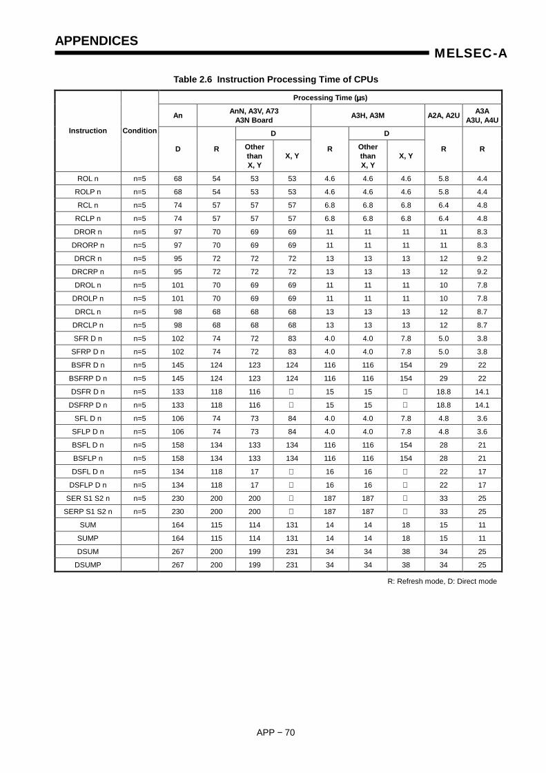
APPENDICES
APP − 70
MELSEC-A
Table 2.6 Instruction Processing Time of CPUs
Processing Time (µµµµs)
An AnN, A3V, A73 A3N Board A3H, A3M A2A, A2U A3A
A3U, A4U
D D Instruction Condition
D R Other than X, Y
X, Y R Other
than X, Y
X, Y R R
ROL n n=5 68 54 53 53 4.6 4.6 4.6 5.8 4.4
ROLP n n=5 68 54 53 53 4.6 4.6 4.6 5.8 4.4
RCL n n=5 74 57 57 57 6.8 6.8 6.8 6.4 4.8
RCLP n n=5 74 57 57 57 6.8 6.8 6.8 6.4 4.8
DROR n n=5 97 70 69 69 11 11 11 11 8.3
DRORP n n=5 97 70 69 69 11 11 11 11 8.3
DRCR n n=5 95 72 72 72 13 13 13 12 9.2
DRCRP n n=5 95 72 72 72 13 13 13 12 9.2
DROL n n=5 101 70 69 69 11 11 11 10 7.8
DROLP n n=5 101 70 69 69 11 11 11 10 7.8
DRCL n n=5 98 68 68 68 13 13 13 12 8.7
DRCLP n n=5 98 68 68 68 13 13 13 12 8.7
SFR D n n=5 102 74 72 83 4.0 4.0 7.8 5.0 3.8
SFRP D n n=5 102 74 72 83 4.0 4.0 7.8 5.0 3.8
BSFR D n n=5 145 124 123 124 116 116 154 29 22
BSFRP D n n=5 145 124 123 124 116 116 154 29 22
DSFR D n n=5 133 118 116 15 15 18.8 14.1
DSFRP D n n=5 133 118 116 15 15 18.8 14.1
SFL D n n=5 106 74 73 84 4.0 4.0 7.8 4.8 3.6
SFLP D n n=5 106 74 73 84 4.0 4.0 7.8 4.8 3.6
BSFL D n n=5 158 134 133 134 116 116 154 28 21
BSFLP n n=5 158 134 133 134 116 116 154 28 21
DSFL D n n=5 134 118 17 16 16 22 17
DSFLP D n n=5 134 118 17 16 16 22 17
SER S1 S2 n n=5 230 200 200 187 187 33 25
SERP S1 S2 n n=5 230 200 200 187 187 33 25
SUM 164 115 114 131 14 14 18 15 11
SUMP 164 115 114 131 14 14 18 15 11
DSUM 267 200 199 231 34 34 38 34 25
DSUMP 267 200 199 231 34 34 38 34 25
R: Refresh mode, D: Direct mode
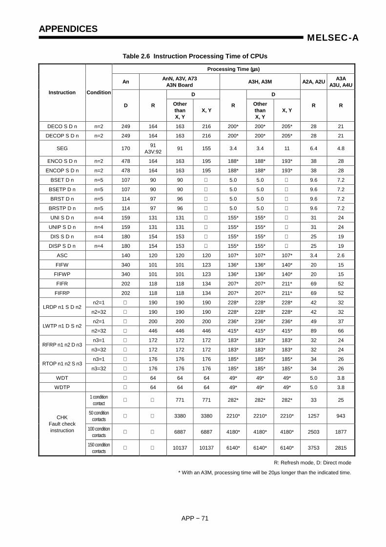
APPENDICES
APP − 71
MELSEC-A
Table 2.6 Instruction Processing Time of CPUs
Processing Time (µµµµs)
An AnN, A3V, A73 A3N Board A3H, A3M A2A, A2U A3A
A3U, A4U
D D Instruction Condition
D R Other than X, Y
X, Y R Other
than X, Y
X, Y R R
DECO S D n n=2 249 164 163 216 200* 200* 205* 28 21
DECOP S D n n=2 249 164 163 216 200* 200* 205* 28 21
SEG 170 91 A3V:92 91 155 3.4 3.4 11 6.4 4.8
ENCO S D n n=2 478 164 163 195 188* 188* 193* 38 28
ENCOP S D n n=2 478 164 163 195 188* 188* 193* 38 28
BSET D n n=5 107 90 90 5.0 5.0 9.6 7.2
BSETP D n n=5 107 90 90 5.0 5.0 9.6 7.2
BRST D n n=5 114 97 96 5.0 5.0 9.6 7.2
BRSTP D n n=5 114 97 96 5.0 5.0 9.6 7.2
UNI S D n n=4 159 131 131 155* 155* 31 24
UNIP S D n n=4 159 131 131 155* 155* 31 24
DIS S D n n=4 180 154 153 155* 155* 25 19
DISP S D n n=4 180 154 153 155* 155* 25 19
ASC 140 120 120 120 107* 107* 107* 3.4 2.6
FIFW 340 101 101 123 136* 136* 140* 20 15
FIFWP 340 101 101 123 136* 136* 140* 20 15
FIFR 202 118 118 134 207* 207* 211* 69 52
FIFRP 202 118 118 134 207* 207* 211* 69 52
n2=1 190 190 190 228* 228* 228* 42 32 LRDP n1 S D n2
n2=32 190 190 190 228* 228* 228* 42 32
n2=1 200 200 200 236* 236* 236* 49 37 LWTP n1 D S n2
n2=32 446 446 446 415* 415* 415* 89 66
n3=1 172 172 172 183* 183* 183* 32 24 RFRP n1 n2 D n3
n3=32 172 172 172 183* 183* 183* 32 24
n3=1 176 176 176 185* 185* 185* 34 26 RTOP n1 n2 S n3
n3=32 176 176 176 185* 185* 185* 34 26
WDT 64 64 64 49* 49* 49* 5.0 3.8
WDTP 64 64 64 49* 49* 49* 5.0 3.8
1 condition contact 771 771 282* 282* 282* 33 25
50 condition contacts 3380 3380 2210* 2210* 2210* 1257 943
100 condition contacts 6887 6887 4180* 4180* 4180* 2503 1877
CHK Fault check instruction
150 condition contacts 10137 10137 6140* 6140* 6140* 3753 2815
R: Refresh mode, D: Direct mode
* With an A3M, processing time will be 20µs longer than the indicated time.
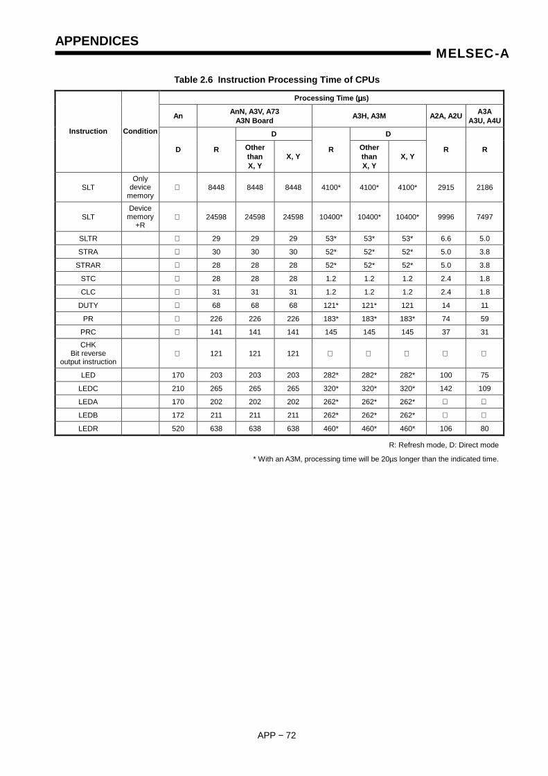
APPENDICES
APP − 72
MELSEC-A
Table 2.6 Instruction Processing Time of CPUs
Processing Time (µµµµs)
An AnN, A3V, A73 A3N Board A3H, A3M A2A, A2U A3A
A3U, A4U
D D Instruction Condition
D R Other than X, Y
X, Y R Other
than X, Y
X, Y R R
SLT Only
device memory
8448 8448 8448 4100* 4100* 4100* 2915 2186
SLT Device
memory+R
24598 24598 24598 10400* 10400* 10400* 9996 7497
SLTR 29 29 29 53* 53* 53* 6.6 5.0
STRA 30 30 30 52* 52* 52* 5.0 3.8
STRAR 28 28 28 52* 52* 52* 5.0 3.8
STC 28 28 28 1.2 1.2 1.2 2.4 1.8
CLC 31 31 31 1.2 1.2 1.2 2.4 1.8
DUTY 68 68 68 121* 121* 121 14 11
PR 226 226 226 183* 183* 183* 74 59
PRC 141 141 141 145 145 145 37 31
CHK Bit reverse
output instruction 121 121 121
LED 170 203 203 203 282* 282* 282* 100 75
LEDC 210 265 265 265 320* 320* 320* 142 109
LEDA 170 202 202 202 262* 262* 262*
LEDB 172 211 211 211 262* 262* 262*
LEDR 520 638 638 638 460* 460* 460* 106 80
R: Refresh mode, D: Direct mode
* With an A3M, processing time will be 20µs longer than the indicated time.
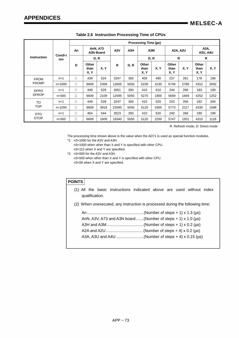
APPENDICES
APP − 73
MELSEC-A
Table 2.6 Instruction Processing Time of CPUs
Processing Time (µµµµs)
An AnN, A73 A3N Board A3V A3H A3M A2A, A2U A3A,
A3U, A4U
D, R D, R R R Instruction Condi-tion
D Other than X, Y
X, Y R D, R Other
than X, Y
X, Y Other than X, Y
X, Y Other than X, Y
X, Y
n=1 439 524 3347 300 400 490 237 261 178 196 FROM FROMP n=1000 6609 2358 12605 5050 5230 3130 5749 2789 4312 2092
n=1 449 529 3051 300 410 610 244 266 183 199 DFRO DFROP n=500 6609 2109 12595 5050 5270 1900 5669 1669 4252 1252
n=1 449 539 3247 300 410 520 243 266 182 200 TO TOP n=1000 6609 3918 22590 5050 5120 3300 5773 2117 4330 1588
n=1 454 544 3523 300 410 520 240 266 180 199 DTO DTOP n=500 6609 1609 19340 5050 5120 2200 5747 1501 4310 1126
R: Refresh mode, D: Direct mode
The processing time shown above is the value when the AD71 is used as special function modules. *1: n3=1000 for the A3V and A3H. n3=1000 when other than X and Y is specified with other CPU. n3=112 when X and Y are specified. *2: n3=500 for the A3V and A3H. n3=500 when other than X and Y is specified with other CPU. n3=56 when X and Y are specified.
POINTS
(1) All the basic instructions indicated above are used without index qualification.
(2) When unexecuted, any instruction is processed during the following time:
An...................................................(Number of steps + 1) x 1.3 (µs) AnN, A3V, A73 and A3N board.......(Number of steps + 1) x 1.0 (µs) A3H and A3M .................................(Number of steps + 1) x 0.2 (µs) A2A and A2U................................. (Number of steps + 4) x 0.2 (µs) A3A, A3U and A4U.........................(Number of steps + 4) x 0.15 (µs)
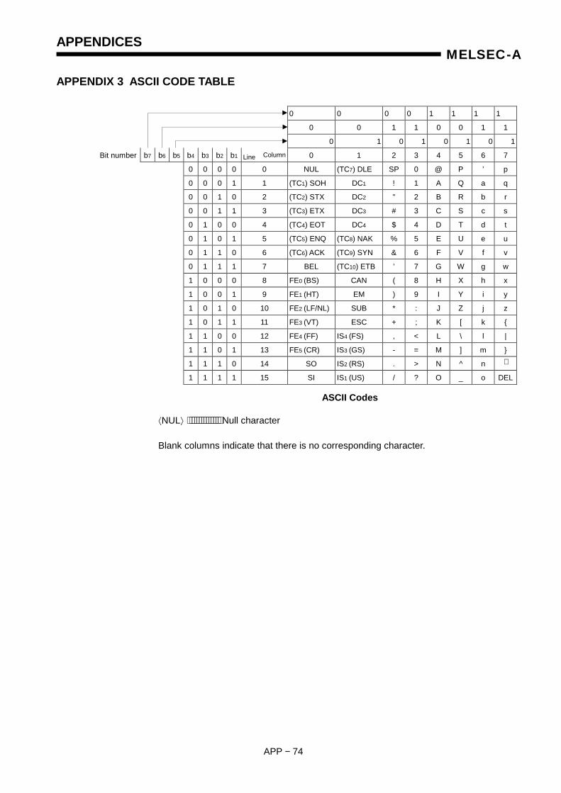
APPENDICES
APP − 74
MELSEC-A
APPENDIX 3 ASCII CODE TABLE
0 0 0 0 1 1 1 1
0 0 1 1 0 0 1 1
0 1 0 1 0 1 0 1
Bit number b7 b6 b5 b4 b3 b2 b1 Line Column 0 1 2 3 4 5 6 7
0 0 0 0 0 NUL (TC7) DLE SP 0 @ P ’ p
0 0 0 1 1 (TC1) SOH DC1 ! 1 A Q a q
0 0 1 0 2 (TC2) STX DC2 " 2 B R b r
0 0 1 1 3 (TC3) ETX DC3 # 3 C S c s
0 1 0 0 4 (TC4) EOT DC4 $ 4 D T d t
0 1 0 1 5 (TC5) ENQ (TC8) NAK % 5 E U e u
0 1 1 0 6 (TC6) ACK (TC9) SYN & 6 F V f v
0 1 1 1 7 BEL (TC10) ETB ’ 7 G W g w
1 0 0 0 8 FE0 (BS) CAN ( 8 H X h x
1 0 0 1 9 FE1 (HT) EM ) 9 I Y i y
1 0 1 0 10 FE2 (LF/NL) SUB * : J Z j z
1 0 1 1 11 FE3 (VT) ESC + ; K [ k {
1 1 0 0 12 FE4 (FF) IS4 (FS) , < L \ l |
1 1 0 1 13 FE5 (CR) IS3 (GS) - = M ] m }
1 1 1 0 14 SO IS2 (RS) . > N ^ n ∼
1 1 1 1 15 SI IS1 (US) / ? O _ o DEL
�NUL� ⋅⋅⋅⋅⋅⋅⋅⋅⋅⋅⋅⋅⋅⋅ Null character
Blank columns indicate that there is no corresponding character.
ASCII Codes
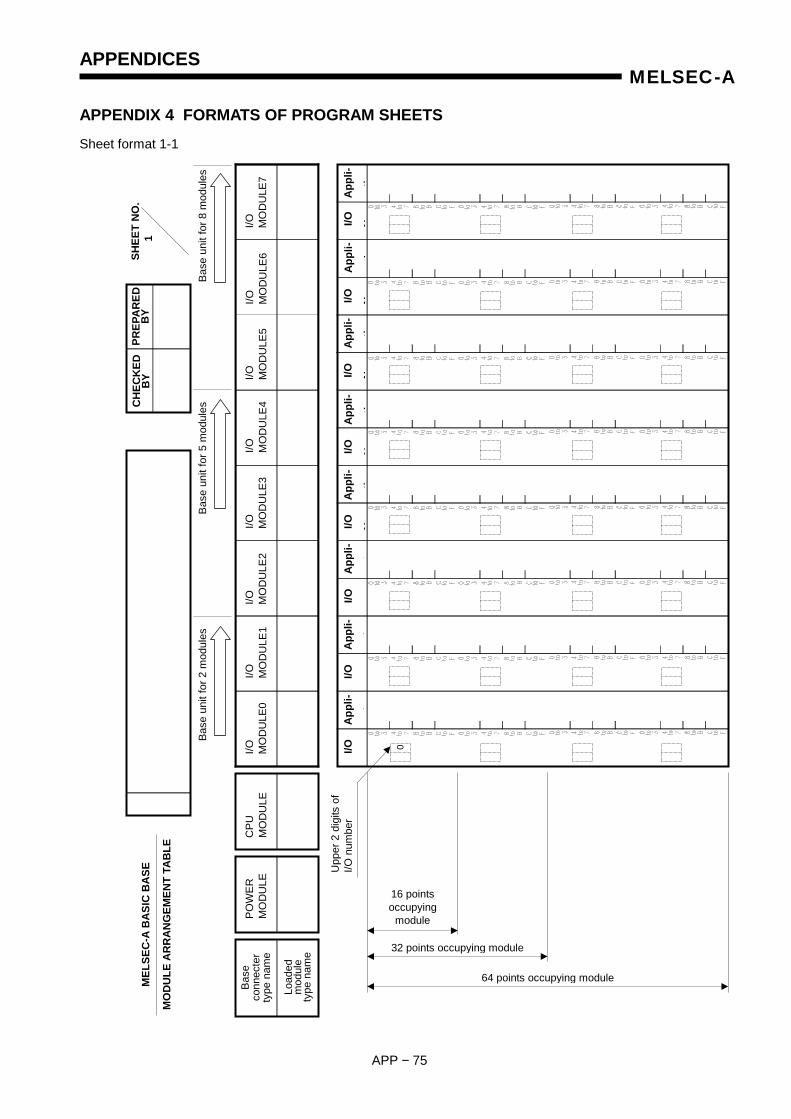
APPENDICES
APP − 75
MELSEC-A
APPENDIX 4 FORMATS OF PROGRAM SHEETS Sheet format 1-1
Base
uni
t for
8 m
odul
es
0
MEL
SEC
-A B
ASI
C B
ASE
MO
DU
LE A
RR
AN
GEM
ENT
TAB
LE
64 points occupying module
32 points occupying module
16 points occupying
module
App
li-
ti
I/O
N
App
li-
ti
I/O
N
App
li-
ti
I/O
N
App
li-
ti
I/O
N
App
li-
ti
I/O
N
App
li-
ti
I/O
N
App
li-
ti
I/O
N
App
li-
ti
I/O
N
CH
ECK
ED
BY
PREP
AR
ED
BY
SHEE
T N
O.
1
I/O
MO
DU
LE7
Base
co
nnec
ter
type
nam
e I/O
M
OD
ULE
0 I/O
M
OD
ULE
1 I/O
M
OD
ULE
2 I/O
M
OD
ULE
3 I/O
M
OD
ULE
4 I/O
M
OD
ULE
5 I/O
M
OD
ULE
6 C
PU
MO
DU
LE
POW
ER
MO
DU
LE
Load
ed
mod
ule
type
nam
e
Base
uni
t for
5 m
odul
es
Base
uni
t for
2 m
odul
es
Upp
er 2
dig
its o
f I/O
num
ber
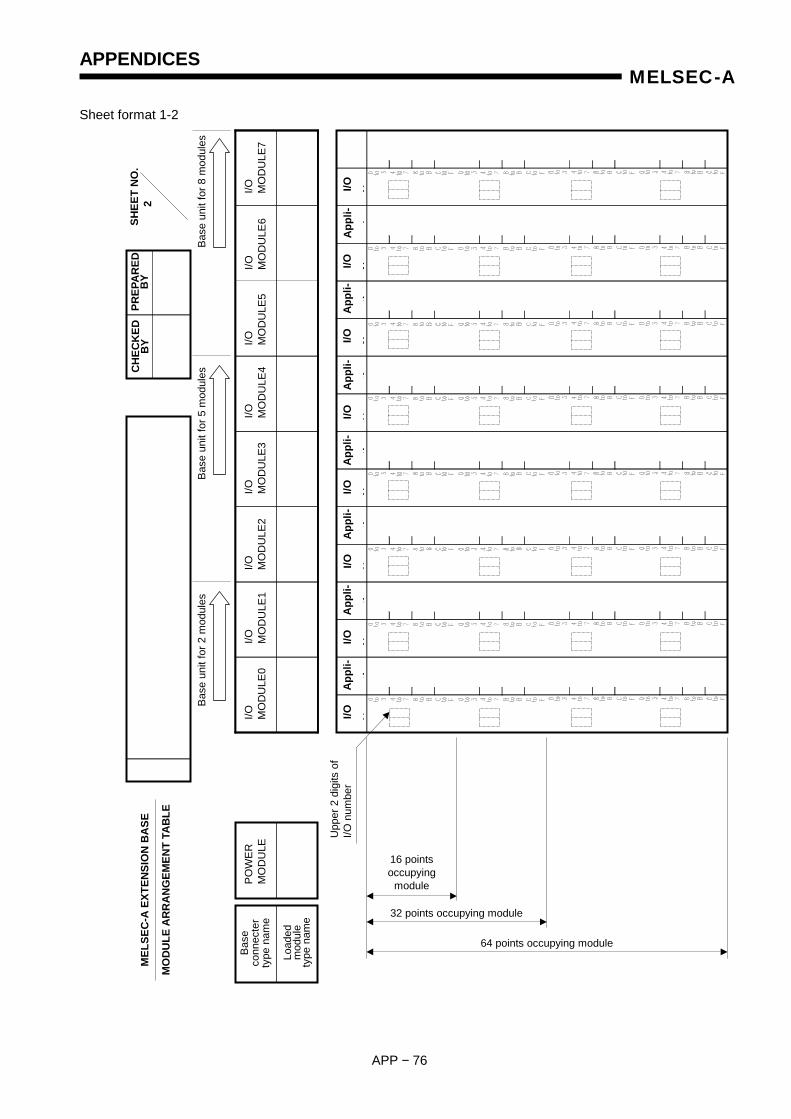
APPENDICES
APP − 76
MELSEC-A
Sheet format 1-2 I/O
M
OD
ULE
7
MEL
SEC
-A E
XTEN
SIO
N B
ASE
MO
DU
LE A
RR
AN
GEM
ENT
TAB
LE
64 points occupying module
32 points occupying module
16 points occupying
module
I/O
N
App
li-
ti
I/O
N
App
li-
ti
I/O
N
App
li-
ti
I/O
N
App
li-
ti
I/O
N
App
li-
ti
I/O
N
App
li-
ti
I/O
N
App
li-
ti
I/O
N
CH
ECK
ED
BY
PREP
AR
ED
BY
SHEE
T N
O.
2
Base
co
nnec
ter
type
nam
e I/O
M
OD
ULE
0 I/O
M
OD
ULE
1 I/O
M
OD
ULE
2 I/O
M
OD
ULE
3 I/O
M
OD
ULE
4 I/O
M
OD
ULE
5 I/O
M
OD
ULE
6 PO
WER
M
OD
ULE
Load
ed
mod
ule
type
nam
e
Base
uni
t for
5 m
odul
es
Base
uni
t for
2 m
odul
es
Upp
er 2
dig
its o
f I/O
num
ber
Base
uni
t for
8 m
odul
es
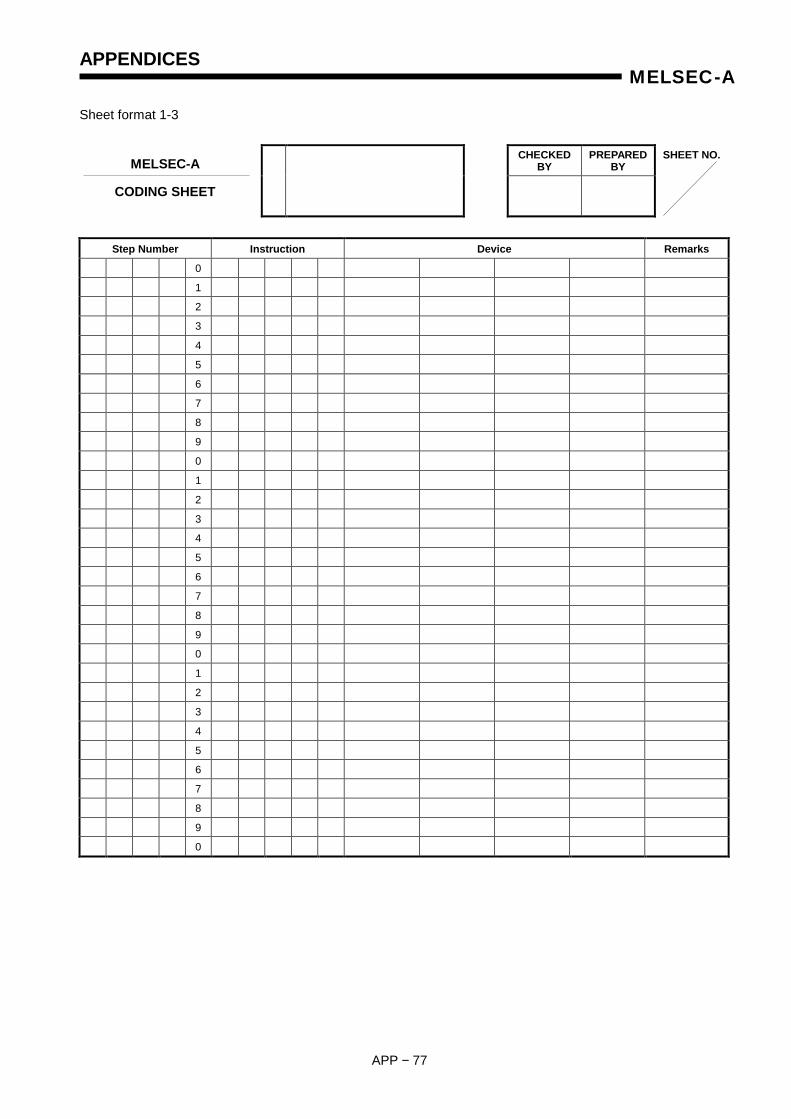
APPENDICES
APP − 77
MELSEC-A
Sheet format 1-3
CHECKED BY
PREPARED BY
SHEET NO.
Step Number Instruction Device Remarks
0
1
2
3
4
5
6
7
8
9
0
1
2
3
4
5
6
7
8
9
0
1
2
3
4
5
6
7
8
9
0
MELSEC-A
CODING SHEET
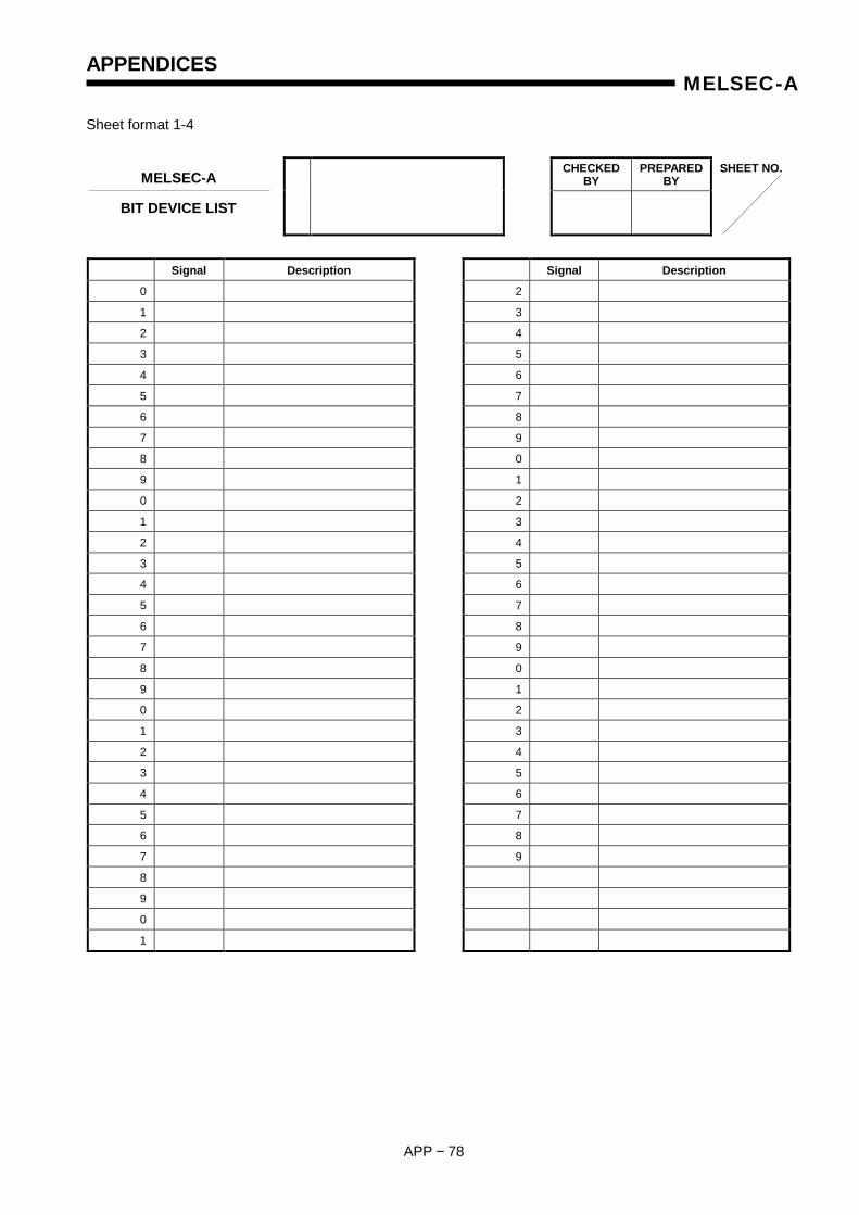
APPENDICES
APP − 78
MELSEC-A
Sheet format 1-4
CHECKED BY
PREPARED BY
SHEET NO.
Signal Description Signal Description
0 2
1 3
2 4
3 5
4 6
5 7
6 8
7 9
8 0
9 1
0 2
1 3
2 4
3 5
4 6
5 7
6 8
7 9
8 0
9 1
0 2
1 3
2 4
3 5
4 6
5 7
6 8
7 9
8
9
0
1
MELSEC-A
BIT DEVICE LIST

APPENDICES
APP − 79
MELSEC-A
Sheet format 1-5
CHECKED BY
PREPARED BY
SHEET NO.
Data (16 bits/data) Description Data
(16 bits/data) Description
0 0
1 1
2 2
3 3
4 4
5 5
6 6
7 7
8 8
9 9
0 0
1 1
2 2
3 3
4 4
5 5
6 6
7 7
8 8
9
9
MELSEC-A
WORD DEVICE LIST
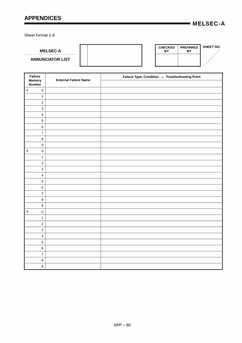
APPENDICES
APP − 80
MELSEC-A
Sheet format 1-6
CHECKED BY
PREPARED BY
SHEET NO.
Failure Type, Condition →→→→ Troubleshooting Point Failure Memory Number
External Failure Name
F 0
1
2
3
4
5
6
7
8
9
F 0
1
2
3
4
5
6
7
8
9
F 0
1
2
3
4
5
6
7
8
9
MELSEC-A
ANNUNCIATOR LIST

APPENDICES
APP − 81
MELSEC-A
Sheet format 1-7
CHECKED BY
PREPARED BY
SHEET NO.
Number Set Value K Description Application, Operation (Count Input), etc.
0
1
2
3
4
5
6
7
8
9
0
1
2
3
4
5
6
7
8
9
0
1
2
3
4
5
6
7
8
9
MELSEC-A
TIMER, COUNTER LIST