Embed Size (px)
Citation preview

MASSACHUSETTS INSTITUTE OF TECHNOLOGY
RADIATION LABORATORY SERIES
LOUIS N. RIDENOUR, Editor-in-Chief
CRYSTAL RECTIFIERS

,-0
MASSACHUSETTS
R DIATION LABORATORY SERIES
Board of Editors
LouIs N. RIDENOUR,ditor-in-Chiej
GEOEQEB.
CoLLIIis, Deputy Editor-in-Chtij
BRITTONHANCE, S. A. GOUDS~, R. G. HERH, HUHERT M. J AMES, J ULIAN K. KNIPP,
JAMES L. LAWSON, IIEON
B. LINFORD,AROLG. MONTGOMERY,
.
NEWTON,ALBERT
M. STONE,LOUISA. TURNER,GEORGEE. VALLEY,R., HERHERT H. WHEATON
1.
2.
3.
4.
5.
6.
7.
8.
9.
10.
11 .
12.
13.
14 .
15 .
16 .
17 .
18 .
19 .
20.
21.
22.
23.
24.
25.
26.
27.
28.
RADAR SYSTEM ENGINEERING—R~d8rwu l
RADAR AIDS TO Navigat ion—Hall
RADAR BEAcoNs—EofIerk
LoriAN-pierce,
McKenzie,
an d
Woodward
PULSE GENERAToRs ~k z.s oe a n d
Lebacqz
MICROWAVE MAGNETRONS—COWLS
KLYSTRONS AND MICROWAVE
T ru oDm -H am itton , Kn ipp, an d Ku per
PRINCIPLES OF MICROWAVE CIRcuITs—Montgomery,
Dicke,
an d Purcell
MICROWAVE TRANSMISSION CIRcuIm-k?agan
WAVEGUIDE HANDBooK—Ma%wu itz
TECHNIQUE OF MICROWAVE MEASUREMENTS—M0n lQotN47~
MICROWAVE ANTENNA THEORY AND DESIGN—SdLJ e7
PROPAGATION OF SHORT RADIO WAvEs—KeTT
MICROWAVE DUFLEXERS-i%u~~~n and Montgomer~
CRYSTAL Rectifiers—ToT?ey and Whitma
MICROWAVE Mrxms—pound
COMPONENTS HAr.mBooIf-Bkxkburn
VACUUM TUBE AMPLIF IERS—Va&?Y and wa l~man
WAVEFOR?dS-Chan@ Hughe8, MacN i chol, Sa yre, and Wd tiamu
ELECTRONIC TIME MEASUREhfENTS-chanCe, Huleizer , MacNiciwl ,
and
William8
ELECTRONIC INSTRUBfENTS-(%.%SWOOd,
Holdam , and MacRae
CATHODE RAY TUBE Dm pLAys—Soiler , Sta r,, a nd
Valley
MICROWAVE REcEIvERs-Van
Voorhia
THRESHOLD SIGNALs—Lawson and
Uhlenb@
THEOBY OF Servomechan isms—J arne8 ,
Nickole, and Phil lipe
RADAB SCANNERS AND RADObiES-CUdY, Karelit z, and Turner
COMPUTING MECHANISMS AND Lm=cms-svobada
lNDKK-HSN~
CRYST L RECTIFIERS
By HENRY C. TORREY
ASSOCIATE PROFESSOR OF PHYSICS
RUTGERS UNIVERSITY
And CHARLES A. WHITMER
ASSOC1&TE PROFIZSSOR
OF
PHYSICS
RUTGERS UNIVERSITY
EDITED BY
S . A. GOUDSMIT
LEON B. LINFORD
J AMES
L.
LAWSON
ALBERT M. STONE
OFFICE OF SCIENTIFIC RESEARCH ANTD DEVELOPh IENT
NATIONAL DEFENSE REsE.4RCH COIIMITTEE
F IRST EDIT ION
SECOND IMPRESSION
NEW YORK AND LONDON
McGRAW-HILL BOOK CO MPA,VY , INC.
1948
CI5
CRYSTAL RE CTIF IE RS
COPYRIGHT, 1948, BY THE
LIcG&w-HILL B OK COMPAXY,
PRIXTED IN THE UNITED ST.iTES OF
INC.
AMERIcA
-411 rights reserved. This book, OT
park thereof, may not be reproduced
in any form without permission oj ,
the publishers.
THE MAPLE PRESS COMPANY, YORK, PA.
o
c1
T
Foreword
T
HE tremendous research and development effor t that wen t into the
development of radar and rela ted techniques dur ing World War II
resulted not only in hundreds of radar sets for milita ry (and some for
possible peacet ime) use but also in a grea t body of informat ion and new
techniques in the elect ronics and high-frequency fields. Because th is
basic m at er ial may be of gr ea t va lue t o scien ce and en gin eer in g, it seemed
most impor tant to publish it as soon as secur ity permit ted.
The Radiat ion Labora tory of MIT, which opera ted under the super -
vision of t he Nat ional Defen se esea rch Commit tee, u nder took t he gr ea t
t a sk of pr epar ing these volumes.
Th e wor k descr ibed h er ein , h owever , is
the collect ive result of work done at many labora tor ies, Army, Navy,
university, and industr ial, both in this count xy and in England, Canada,
and other Domin ions .
The Radiat ion Laboratory, o ce it s proposals were approved and
fin an ces pr ovided by t he Office of Scien tific Resea rch a nd Developmen t,
chose Louis N. Ridenour as Editor -in-Chief to lead and direct the ent ire
project . An editor ia l staff was then selected of those best qualified for
this type of ta sk . Fin a lly th e au th ors for th e va r iou s volu mes or ch ap ters
or sect ions were chosen from among those exper ts who were int imately
familiar with the var ious fields, and who were able and willing to writ e
the summaries of th em . Th is en tire s ta ff agreed to rema in a t work a t
MIT for six months or more after the work of the Radiat ion Labora tory
was complete. These volumes stand as a monument to this group.
These volum s serve as a memorial to the unnamed hundreds and
t housan ds of ot her scient ist s, en gineer s, an d ot her s wh o act ually ca rr ied
on t he r esea rch , developm n t, and en gin eer in g wor k t he r esu lt s of wh ich
are h erein descr ibed . Th ere were so many in volved in th is work an d th ey
worked so clos ely togeth er even th ou gh often in widely s epa ra ted labora -
tories th a t it is impos s ib le to n ame or even to kn ow th os e who con t ribu ted
to a pa rt icu la r idea or developmen t.
On ly certa n on es who wrote repor ts
or a r t icles h ave even been men tion ed.
Bu t to a ll th os e wh o con tr ibu ted
&
in an y way to th is grea t coopera t ive developm en t en terpris e, both in th is
cou n try an d in Englan d, th es e volum es a re dedica ted .
L. A. DUBRIDGE.
m
v

I
v(/
‘-,.

Preface
W
ITH th e developmen t of m icrowave rada r, th e cr s ta l rect ifier ,
wh ich h ad been lit t le u s ed s in ce th e in ven t ion of th e va cu um tu be
s evera l deca des ago, a ga in became impor ta n t -a s importa n t a s th e magn e-
tron , k lys tron , or oth er m icrowave compon en ts .
In th e pa s t five yea rs crys ta l rect ifiers h ave been manu fa ctu red ,
litera lly by th e m illion s , for u s e pr ima rily a s m icrowave detectors . A
corres pon d in gly la rge amou n t of fu n damen ta l res ea rch an d en gin eer in g
developm en t h a s ta ken p la ce in th e commercia l an d governmen ta l la bora -
tor ies in th e Un ited Sta tes an d in En glan d . As a res u lt th e crys ta l-
rect ifier u n it th a t h a s emerged is a compact , s ta b le d evice wh ich is su per ior
in many app lica t ion s to th e va cu u m -tu be d iode. It s mos t exten s ive u s e
u p to n ow h a s been a s a frequ en cy con ver ter in m icrowave recep t ion ,
wh ere it s per forman ce h a s n ot been equ a led . It h a s a ls o b een u s ed to a
les s er exten t a s a low-level m icrowave detector .
Th e recen t developmen t of german ium rectifiers capable of with s ta n d -
in g rela t ively h igh in vers e volta ges h old s grea t p rom ise for app lica t ion s
a s s econ d detectors in wideban d receivers an d in a va r iety of oth er cir-
cu it s wh ere va cu um -tu be d iodes a re ord in a rily u s ed .
Th e pu rpos e of th is book is to p resen t th e fu n d of kn owledge on crys ta l
rect ifiers th a t h a s a ccu mu la ted du r in g th e cou rs e of World War 11 .
Beca u s e of th e n eed in rada r s ys tem s for h igh -qu a lity m icrowave con -
ver ters , a la rge fra ct ion of th e work wa s expen ded for th e develop -
men t of crys ta l rect ifiers for th is a pp l ca t ion .
A corres pon d in gly la rge
fra ct ion of th e book has, t her efor e, been devot ed t o t he t heor y an d pr oper -
t ies of t he cr yst al conver ter . Ot her applicat ions ar e discussed in Par t III
a s Specia l Types .
As in every other branch of microwave work, the development of
measur ing equipment and techniques has t aken place simultaneously
with that of the crysta l r ect ifier it self. We have, therefore, included
deta iled discussions of methods of measurement of cryst a l proper t ies
and a descr ipt ion of standar d t est equipment for pr odu ct ion and r out ine
testing.
Th e t echn iqu es for m an ufact ur in g con ver ter cr yst als a re discus ed in
Chap. 10. Special t echniques required for the manufacture of other
types are descr ibed in the appropr ia t e chapter s. The procedures pre-
sented in deta il a re drawn largely from the work done at the MIT
vii

...
Vm
PREFACE
Radiat ion Labora tory and by NDRC contractees, but no at tempt has
been made toinclude the deta ils of all of the procedures that have been
successful ly employed.
Because of the unique nature of war research and de elopment , it
is impossible to acknowledge adequately individual cont r ibut ions to
th is subject . Much of the work is a result of the joint effor t s of many
individuals. At the present writ ing most of the available litera ture
is in the form of repor t s that , for reasons of secur ity, have not yet been
pu blish ed in scien tific jour nals.
Much of the litera ture refer red to
will undoubtedly appear la ter , however , in journal ar t icles, or will be
declassified and made available by the United Sta tes government .
We have therefore given references to some of the more impor tant of
these documents .
In England the chief contr ibutors to crysta l research and develop-
m en t wer e t he Gen er al E lect r ic Compan y, Br it ish Thompson -Hou st on ,
Ltd., Telecommunicat ions Research Establishment, and Oxford Uni-
versity; in th is count ry they were the Bell Telephone Laborator ies,
West in ghou se Res ea rch Labor at or y, Gener al E lect r ic Company, Sylvania
Elect r ic Products, Inc., and E. I. duPont de Nemours and Company.
The crystal groups at the Univer sity of Pennsylvania and Purdue Uni-
1
ver sit y, wh o oper at ed u nder NDRC con tr act s, wer e r espon sible for much
of t he fundamental resear ch and development wor k r epor ted her ein .
DuPont and the Eagle-Picher Company developed manufactur ing
pr ocesses a nd pr odu ced in qu an tit y h igh l y pu rified silicon a nd germanium
oxide, r espect ively, without ]vhich much of th e improvement in cr ystal
r ect ifier s wou ld have been impos sible.
We are par t icular ly indebted to our colleagues at the Radia t ion
Labor atory whose contr ibut ions and st imulat ing discussions have been
in valuable in wr it in g t his book.
The prepara t ion of th is manuscr ipt would have been impossible,
finally, without the splendid aid of the editor ia l staff. In addit ion to
those names listed as editors, we wish par t icular ly to emphasize our
gra t itude to Barbara E. Myers, Mar jor ie S. Tar iot , and Natalie C.
“Tucker , editor ia l assis tants .
~
HENRY C. TORREY.
CHARLESA. WHITMER.
CAMBIUD~E.ASS.
Contents
FOREWORDBYL. A. DUBRIDGE .
PREFACE. . . . . . . . . . . . . . . . . . . . . . . . . . . .
CHAP.. INTRODUCTION . . . . . . . . . . . .
THEPHENOMENONFRECTIFICATION
11, The Non lin ea rElemen t .
1.2. Detect ion ..,.,,. . . . . . . . . . . . . . .
13. F requencyConvers ion
THENATUREOFTHECBYSTALECTIF IEB
1.4.
The Discovery and Ear ly Use of Crystal Rectifiers.
1 .5. Recent Developments
PART I. GENERAL PROPERTIES
.
v
vii
,.
CHAP. 2. FUNDAMENTAL PROPERTIES OF THE CRYSTAL RECTI-
FIER . . . . . . . . . . . . . . . . . . . . . . .
THE PRESENT CRYSTAL CARTRIDGES. ., . .
2.1. Descript io of the Cart r idge .
2.2, Stability and Handling Precaut ions. . . . . .
ELECTFUCALPROPERTIES . . . . . . . . . . . . . . . . . . . . . .
2 ,3 . Th e Volta ge-cu rren t Ch ara cteris tic
2 .4. Th e Equ iva len t Circu it .
MIXER CRYSTALS . . . . . . . . . . . . . . . . . . . . . .
2 .5 . Con vers ion Loa s, Noise, and Noise Figure.
2.6. Optimum Local-oscillator Level
2.7. The R-f Impedance of Crystal Rectifim-s
2.8. The I-f Impedance of Crysta l Rect ifiers .
CHAP. 3 . PROPERTIES OF SEMICONDUCTORS. .
3 .1. Ban d Th eory.....,.. . . . . . . . . . . .
3 .2. Electron Dis tr ibu tion in Sem icon du ctors
3 .3. Work Fu nction s rind Con ta ct Poten tia ls
3 .4. Electr ica l Con du ctivity an d. Ha ll Cocfficicn t for Sem icon du ctors
3 .5. Ch aracter is t ic Con stan ts of Silicon a nd Germa nium
3.6. Effect of Impurity Addit ions in Silicon and Germanium,
1
1
1
2
4
5
5
6
15
15
15
18
20
20
23
25
25
33
35
40
45
45
48
51
53
61
64
ix

i
i
x
CONTENTS
CHAP. 4. THE S13MICO~DUCTOR-METAL CONTACT . 68
41 .
4.2.
43 .
4,4.
4.5.
4.6.
Barrier -layer Rectificat ion . . 68
Formation and Structure of the Barr ier Layer. 70
Diffusion and Diode Theories of Rectificat ion . . 77
The D-c Characterist ic. . 82
Deplet ion Layers ...,..,. . . . . . . . . . . ...90
Rectifica t ion at High Frequencies . . 97
PART II. THE CRYSTAL CONVERTER
CHAP. 5. FREQUENCY CONVERSION. 111
5.1. Discussion of the General Problcm. 111
5.2. The Admittance Matr ix. 114
THE PHENOMENOLOGICALTHEORY ON CONVERSION 119
53. The Admit tance Matr ix
in
Terms of Measurabk 1%-amet rs 119
5.4. Transformation of the Matrix to New Variables 121
5.5. Reciprocity . . . . . . . . . . 124
CONVERSION Loss AND MIXER ADMITTANCES 1 8
56. General Defin it ion of Loss; Specia l Cases 128
57. Con ersion Loss in t he Broadba d Case. 130
58. Ge era l Expr ssion for Conversion Loss. 136
5.9. Effect of the Image Termination on Conversion Loss. 140
5,10. Effect of Image Termination on I-f Impedance. 148
THE PHYSICAL THEORY OF CONVERSION . 152
511. Matr ix of a Nonliiear Resistance 153
5.12. Effect of Parasit ic Impedances on Conversion Loss. 157
5.13. Effect of a Variable Barrier Capacitance . . . 163
5.14. H armonic Reinforcement 167
5.15. Conversion with a Subh rmonic Local Oscillator . 170
5.16. Harmonic Generat ion . . . . . . . . . . 173
5.17. Modulat ion . . . . . . . . . . . . . . . . . . . . . . 174
CHAP.6. NOISE GENERATION. . . . . . .17’9
THEOR . . . . . . . . . . . . . . . . . . . . . . . . . . . .. 179
6.1. Shot and Thermal Noise iD Crystal Rectifiers 179
6.2. Other Sources of Noise. . . .186
lNTER?JEDMTE-FREQUENCY AND VIDEO NOISE, . . 187
6.3. Dependence of Noise Tempera ture on Frequency, . . 188
6.4. Dependence on Temperature . . . . 194
MICROWAVE NOE.E . . . . . . . . . . . . . . . . . . . . . . . .. 195
65. Th e Crys ta l a s a Microwave Noise Gen era tor . . . . . . 195
CHAP. 7. LOSS AND NOISE MEASUREMENTS. . . . . . . . . 198
LOSS MEASUREMENTS . . . . . . . . . . . . . . . . . . . . . . .. 198
7.1 . en era l Con s idera t ion s . . , , . , , . . . , . . . 198

CONTENTS xi
7.2. The Heterodyne Method . . . . . . . 200
73. Impedance ~fethOds . . . . . . . . . . . . . . . . . . . ..2o2
74. The Incrementa l and Amplitude-modula t icm J lcthods 213
LVOISl+TEl~PllRATURE hfMA5UREM~NT5 . 218
7,5. Genera l Con ider t ions. . 218
76. The Rober t s Coupling Circu it . 223
7.7. Nar row-band Coupling Circuit . 225
78. Use of the Noise Diode in Noise-tempera tu re Measu rement s. 226
MEASUREMENT OF Loss, NOISE, AND RECEIVER NOISE FIGURE 227
7.9. The Measurement of Receiver Noise Figure. 227
710. The Measurement of Mixer -crysta l P roper t ies. . 230
7.11. Loss and Noise Tempera tu re as a Funct ion of R-f Tuning. 232
CHAP. 8. BURNOUT . . . . . . . . 236
8,1. Genera l Considera t ions. 236
82. BurnoutT henry . . . . . . . . . . . . . . . . . . . ...239
8.3. Burnout Theory . . . . . . 248
84. Exper iment s on Burnou t 256
8.5. Burnou t Limita t ions of Standard Crysta l Unit s . 260
CHAP. 9. TEST EQUIPMENT . . . . . . . . . . . . . . . . . . ...264
STANDARD LOSS TEST SETS. . . . . . .264
9.1. The Conver sion-loss Set for the 3-cm Band . 265
92. The Conversion-loss Set for the lo-cm Band. 272
9.3. The Conversion -loss Set for the l-cm Band 276
9.4. The Mechanica l Modula tor 280
STANDARD NOISE TEST SETS. . . . . . . . . . . .283
95. The Noise Measur ing Set for the 3-cm Band. . 283
96. The Noise Measur ing Set for the 10-cm Band . . 289
9.7. Noise-tempera ture Measurement of l-cm Rect ifier . 292
BuRNouT. . . . . . . . . . . . . . . . . . . . . . . .293
98. S pikeT est . . . . . . . . . . . . . . . . . . . . . ...293
99. Microsecond Pulse Test . . . . . . . 296
FIELD TESTING . . . . . . . . . . . . . . . . . . . . . . . . . .. 297
910. D-cTests . . . . . . . . . . . . . . . . . . . . . . . . . 297
CHAP. 10. MANUFACTURING TECHNIQUES . . . . . . . . . . . . . 301
PREPARATION OF SEMICONDUCTOR. . . . . . . . . . . . . 301
10.1. Pur ifica t ion of the Semiconductor . . . . . . . . . . . . 301
10.2. Addit ion Agent s . . . . . . . . . . . . . . . . . . . . . .306
10.3. Prepara t ion of the Ingot . . . .308
10.4. Polish ing, Heat -t r ea tment , and E tching. . . . 314

xii
CONTENTS
THE CAT WHISKER . . . . . . . . . . . . . . . . . . . . . .. 316
10.5 . Wh isker Ma ter ia ls . . . . . . . . . . . . . . . . . . ...316
10.6 . Fab rica t ion of th e Wh isker . . . . . . . 318
ASSEMBLY AND ADJ USTMENT OF THE CARTRIDGE. . . . . . . . 323
10.7 . Th e Ceram ic Ca rtr idge. . . . . . . 323
10.8 . Th e Coaxia l Ca rtr idge . . . . . . . . . . . . . . . . ...326
SOME DESIGN CONWDERATIONSAFFECTING ELECTF tlCAL PERFORMANCE . 328
10.9. R-f Impedance . . . . . . . . . . . . . . . . . . . . . . .328
10.10. Conversion Loss and Burnout . . . 329
PART III. SPECIAL TYPES
CHAF. 11. LOW-LEVEL DETECTION. . . . . 333
PROPERTIES OF CRYSTAL RECTIFIERS AT Low LEVELS . . . . . . 333
111. Rectifica t ion at Low Levels . . 333
11.2. Equivalent -circu it Theory. . 335
11.3. E ffect of Bias on Low-level Proper t ies . . 340
11.4. Var iat ion of Low-level Proper t ies with Tempera ture . 342
THEORY OF LOW-LEVEL DETECTION 344
11,5. The Figure of Mer it of a Video Crysta l.
344
11.6. E ffect of D-c Bias on Figure of Mer it , 347
11.7. The Effect of Tempera ture Variat ion on Crysta l-video Receiver
Performance . .,..,..., . . . . . . . . . . ...348
M~AsuREMENTs .,..... . . . ...349
118. R-f Equipment a d Measurements, 3 0
119. Equipment and Methods f r Measur i g Current Sensit ivity, Video
Resi tance, and F igure of Mer it . 35
SP~.IXAL MAN UFACTURKN~TECHNIQUES. 3,57
11.10. Stability Considera t ions. 358
11.11. Processing the Silicon . 358.
11.12. Fabr icat ion of the Whisker
359
11.13. Adjustment of t he Rect ifying Contact 359
CHAP . 12. HIGH-INVERSE-VOLTAGE RECTIFIERS 361
THE HIGH-INVERSE-VOLTAGE RECTIFIER AND ITS APPLICATIONS 361
12,1.
12.2.
12.3.
12.4.
12.5.
12.6.
12.7.
12,8.
Preparat ion of the Ingot.
364
Etching and Surface Trea tment
369
Asse bly and Adjustment of the Car t r idge
369
Low-frequency Proper t ies. 372
High-frequency Proper t ies 378
Silicon High-inverse-voltage Rectifiers 389
Theory of the Negative-resistance Character ist ics 391
Phot elect r ic J ;ffccts in Silicon and Germanium 392
CONTENTS
. . .
XII 1
CHAP.
13. WELDED-CONTACT GERM.4NIUM CRYSTALS. 39s
13.1.
13.2.
13.3.
13.4.
135.
13,6.
Const ruct ion of Welded-contact Rectifiers. 398
Genera l Proper t ies .,....,. . . . . . . . . . . ...400
Negative I-f Conductance. 401
Loss and Noise h’measurements, 403
Theory of Negative I-f Conductance and Conversion Amplifica t ion 406
Applicat ions . . . . . . . . . . . . . . . . . . . . . ...415
APPENDIX A The Reciprocity Theorem of Dickc 417
APPENDIX B Skin Effect a t a Meta l-semiconductorCon tact . 421
1
APPENDIX C Spread ingResis t anceof an Ellip tica l
Contact . 427
APPENDIX D Crystal-rect ifier Types and Specifica t ions. . 429
)
‘,
I


CHAPTER 1
INTRODUCTION
THE PHENOMENON OF RECTIF ICATION
The process of rect ifica t ion and its applica t ions a re well known and
extensively t r ea ted in the litera ture.
However , with in the last five
yea rs a wea lt h of n ew in forma tion on t he cr yst al r ect ifier h as a ccumu la ted
as a resu lt o its super ior performance in microwave receive s. In fact ,
t he u se of cr yst al r ect ifier s for fr equ en cy con ver sion occu rr ed for t he fir st
t ime dur ing World War II. The purpose of th is book is to give an
accoun t of the presen t sta te of ou r kn owledge of the crysta l r ect ifier and
its applica t ions. The appli a t ions with which we are chiefly concerned
have to do with the use of the rect ifier as a nonlinear device in the detec-
t ion and frequency conversion of r -f signals. As a background for the
analysis of the crysta l r ect ifier we shall begin with a br ief review of the
pr ocess of det ect ion a nd fr equ en cy con ver sion .
1.1. The Nonlinea r Elemen t .—Rect ifica t ion may be defined as an
oper at ion on a n a -c volt age t o pr odu ce a u nidir ect ion al compon en t.
Th e
vacuum-tube diode s a familiar example of a device tha t per forms this
funct ion . The un idirect iona l componen t ar ises from the fact tha t the
aver age resistan ce t o cu rr en t f ow is less in on e direct ion th an in t he ot her .
In addit ion to the d-c componen t in the rect ifier ou tpu t there a re a lso
pr esen t h armon ics of t he in pu t sign al wh ich a rise beca use of t he n on lin ea r
character of the rect ifying elemen t . The rela t ive amplitudes of the
harmonics depend on the shape of the curren t -voltage character ist ic
cu rve in the opera t ing region . The magn itude of the d-c componen t
a lso depen ds on th e sha pe of t he ch ara cter ist i .
For example, it is clear
tha t a nonlinear element having the character ist ic cu rve of Fig. 1. la ,
wh ich is an odd funct ion of the volt age abou t the or igin , will have no
outpu t d-c componen t a t a ll when opera ted at zero bias.
However , if a
d-c bias volt age is applied so tha t the opera t ing point is a t A, the applica-
t ion of a small a -c signal will r esu lt in a net increase in the direct cu rren t
o er tha t pr duced by the bias a lone.
This occu rs beca use th e a vera ge
cur ren t will be grea ter for the posit ive swings of the a-c signal than for
t he n ega ti;e on es.
Rect ifier s t ha t a re u sefu l for det ect ion pu rposes h ave ch ar act er ist ics
similar to tha t shown in Fig. 1. lb. The shape of the character ist ic will
of cou rse depend on the physica l na tu re of the rect ifier .
In genera l, the
2
IN TIK)DUCTION
[SEC. 12
impor tan t fea tu res a re a high back resist ance and a rela t ively low for -
wa rd r esist an ce. At h igh fr equ en cies ot her ph ysica l ch ar act er ist ics, su ch
as ca pacitan ce of t he r ect ifyin g elem en t, t ra nsit t ime, et c., a re impor tan t
factors. In the vacuum-tube diode, for example, the resistance in the
back direct ion is very h igh. In the forward direct ion the cur ren t is
+
i
A
e
(a)
I m
FIG. 1.l.—Non lin ea r ele-
m e n ts. (a ) Nonrect ifying
elemen t a t zero bias; (b)
rect i fying element ,
propor t ional to the three-ha lves power of the
applied volt age when the volt ages a re small.
For la rger voltages there is a region tha t is ap-
p roxima t ely lin ea r .
As we shall sce la ter , the
sh ape of t h e cr yst a l-r ect ifier ch a ra ct er ist ic may
vary widely depending on the natu re of the
crysta l and thewavinw hich it is const ructed.
We sh all post pon e t he discu ssion of t he cr yst al-
r ect ifier ch ar act er ist ic a nd t he con sider at ion of
theother proper t ies tha t a re of impor tance in
t he m icr owave r egion .
i
/
e
~IG.
1.2.—Ided
mrtifier
characteristic,
1.2. Detect ion .—In the use of the rect ifier for detect ion th ere a re two
classifica t ions tha t a re of par t icu lar in terest to us: (1) linear and (2)
square-law detect ion .
L inea r Det ect ion .—In linea r detect ion , t h r ect ifier fu nct ion s essen-
t ia lly as a switch . Let us assume th at th e rect ifier cha ra cter ist ic is idea l—
that is, tha t t e resistance in the back direct ion is infin ite, and in the for-
ward direct ion is small and constant (see Fig. 1.2). It is well known
that wh en a sinusoidal wa ve is impr essed on th e idea l r ect ifier th e a ver age
cur ren t th rough th is rect ifier will be propor t iona l to the amplitude of
the inpu t wave. The voltage across the rect ifier load resistance will
then be compose of a d-c componen t propor t iona l to the amplitude of
the input signal plus component s of the inpu t frequency and its even
harmonics.
Most rect ifier s will approximate th is idea l per formance if the input
signal is la rge enough to make the region of curva tu re nea r the or igin
small com par ed with t he substant ia lly st ra ight par t of th e ch ara cter ist ic
over which t e voltage var ies. Fur thermore, the load resistance is usu-
SEC.1-2]
DETECTION
3
ally chosen large compared with th e rect ifier resistan ce so tha t t he effect
on t he ou tpu t volt age of va ria tion of t he forwa rd r esista nce of t he r ect ifier
is small.
Th e efficien cy of r ect ifica tion is defin ed as t he r at io of t he d-c volt age
across t e outpu t load resistance to the peak amplitude of the input
signal. It depends on the ra t io of load resistance to the in terna l resis-
ance of the rect ifier and the amplitude of the input signal as noted above.
In the detect ion of amplitude-modula ted waves in radio recept ion a
load consist ing of a para llel RC combinat ion is commonly used. With
proper choice of the values of R and C the output voltage will, t o a very
close a ppr oximat ion , va ry like t he en velope of t he amplit ude-modu la ted
I
wave. Under these condit ions, the rect ifica t ion efficiency of vacuum-
tube diode rect ifiers is normally about 70 to 90 per cen t . A deta iled
analysis of linear detect or s used in radio receiver s may be found in stand-
ard textbooks on radio engineer ing and will not be given here.
r etu rn to a discussion of the use of one of the crysta l rect ifier types as a
linear detector in Chap. 12.
“S quare-law Detect ion .—The
t erm square-law is applied to a det ctor
in which the d-c, or rect ified, output is propor t iona l to the square of the
amplitude of the input signal. It can readily be seen tha t such a response
depends on the nonlinearity of the character ist ic a t the opera t ing poin t .
~
Over a limited r ange th e cu rren t-voltage character ist ic of a rect ifier can
be r epr esen ted by a Ta ylor expa nsion t erm in at in g in t h squ ar ed t erm
(1)
wh er e eOis t he bias volt age det ermin in g t he oper at in g poin t, an d c$eis t he
small input signal voltage. The der iva t ives a re evalua ted at the opera t -
ing poin t eo. Any rect ifier will, t herefore, funct ion as a square-law
rect ifier when the applied signal is sufficien t ly small, provided tha t the
second der iva t ive of the character ist ic does not vanish a t the opera t ing
poin t . The linear term is, of course, of no impor tance as far as rect ifica-
t ion is con cer ned, sin ce it is symmet rica l a bou t t he oper at in g poin t.
By means of Eq. (1) we can determine analyt ica lly the output of the
r ect ifier for a given in pu t sign al.
Th e a na lysis ca n bc summar ized br iefly
as follows. Let us con sider a sign al con sist in g of a sin gle sin usoida l wa ve,
E sin d. In addit ion to the frequency of the signal, the ou tput will
conta in d-c and second-harmonic components with amplitu es pr opor -
t ion al t o E2. In genera l, if the ignal is composed of a number of sinu-
soida l components the ou tput will conta in , in addit ion to the frequency
components of the signal, t he d-c componen t , second harmonics of each
1‘F IX ~xamp[e s ee F , 1?. Term an , Radio Engineer’s Handbook , McGraw-Hill, New
York , 1943,

4
INTRODUCTION
[SEC.
1.3
frequ en cy com pon en t, and sum and difference frequencies formed by
ever y possible combinat ion of frequencies con ta ined in the inpu t signal.
The amplitude of the d-c componen t will be propor t iona l to the sum of the
squares of the amplitudes of the signal componen t s.
The amplitude of
each second-harmonic componen t will be propor t iona l to the square of
the amplitude of the cor responding signal componen t ; the amplitude
of th e sum and difference frequencies will be propor t iona l to th e produ ct
of th e amplitude of the inpu t componen t s involved in the combina t ion .
As an example, let us consider the square-law detect ion of an ampli-
tu de-m odu la t ed wa ve given by t he expr ession
e = ~o(l + m sin @t ) sin t it .
For pu rposes of an alysis th is wa ve may be repr esen ted by t hr ee fr equ en cy
componen ts, the ca r r ier and two sidebands, with angu lar fr equencies
!L_L
33
~N
Frequency
(b)
FIG. 1.3 .—Frequencies involved in
d et ect ion . (a ) F requ en cies in det ect or
in pu t (m odu la tion per cen ta ge = 50);
(b) addit iona l frequen cies in t he de
tector ou tpu t .
u , (~ — B), and (u + B), respect ively.
These a re represen ted graphica lly in
Fig. 1.3a . The rela t ive amplitudes of
the addit ional compon en t s in the ou t-
pu t of the detector a re shown in Fig.
1.3b for the case where m = 0.5.
Th e squ are-law det ect or is a u seful
device for the measurement of the
power of an a-c signal because the rec-
ified ou tpu t is propor t iona l to the
square of the input amplitude. As we
shall see la ter , th e crysta l r ect ifier is
oft en employed as a square-law de
t ect or in mon it or in g m icr owave power .
In fact , such a device is serviceable
ou t side t h e squ a re-law r egion p rovided
it is ca libr at ed.
It is clea r tha t the magn itude of
the va r ious componen ts ar ising from
the square term of Eq. (1) will be pro-
por t iona l to the magn itude of the sec-
on d der iva tive of t he ch ara ct er ist ic a t
the opera t ing poin t . Maximum sensit ivity will then be obta ined by
adjust ing the d-c bias so that the opera t ing poin t is a lso the poin t of max-
imum cu rva tu re on t he ch ar act er ist ic.
Ot her fa ct or s of im por ta nce in t he
m icr owa ve r egion , su ch a s ca pa cit an ce, n oise gen er at ion , et c., will be dis-
cussed in Chap. 11.
1.3. F requ en cy Con ver sion .—Het er odyn e r ecept ion pr ovides a m ea ns
of conver t ing the ca r r ier frequency of a signal to a new va lue.
This is

SEC. 1.4] EARLY USE OF CRYSTAL RECTIFIERS
5
accomplished by means of a local oscilla tor and a non linear elemen t .
The local oscilla tor outpu t and t e signal a re coupled in to the nonlinear
device, where they genera t~among other frequencies—a frequency
equal t o t h e d iffer en ce between t h e sign al a ndloca l-oscilla tor fr equ en cies.
Usually, a lthough not a lways, the loca l-oscilla tor power level is la rge
compared with the signal level. The local oscilla t ion may have either a
lower or h igher frequency than the signal since it is the difference fre-
qu en cy h ich is u su ally of in ter est . Un der t hese on dit ion s t he n on lin ea r
elem en t in so fa r as it fu nct ion s in t he lin ea r r egion , gen er at es a differ en ce
frequency called the in termedia te frequency, the amplitude of which is
propor t iona l to the signal amplitude and independ n t of the amplitude
of the loca l oscilla tor volt age.
The device tha t conta ins the non linear elemen t and the means for
coupling it to the terminals of the local oscilla tor and to the inpu t and
ou tpu t terminals is ca lled a mixer . The input terminals are used for
applica t ion of signal power and t he output terminals a re u sed for deliver y
of power at the in termedia te frequency. The unit consist ing of mixer
and local oscilla tor is ca lled a ‘ frequency conver t er , ” and the whole
pr ocess is r efer red t o as “ mixing” or ‘‘ fr equ en cy con ver sion . ”
If the signal is an amplitude-modula ted wave, the mixer ou tpu t will
con sist of a ca rr ier a t in termedia te fr equ en cy plu s sideba nds wh ich r epr o-
duce the or igina l modula t ion of the signal. In addit ion , the nonlinea r
elemen t in the mixer will genera te harmonics of the loca l oscilla tor and
th e signal frequencies, sum and differen ce fr equ en cies of all t he applied
signals, an these in tu rn will beat with each other to crea te st ill more
frequencies and so on , ad infin itum. For tuna tely most of these fre-
quencies a re so weak that they can be ignored. However , some of them
are of impor tance since their existence result s in the diversion of power
tha t otherwise would appear in the i-f signal. An evalua t ion of the
impor tance of these component s in microwave receiver s will be given in
Chap. 5.
The nonlinea r device used in frequency conversion may be any type
of detector or demodula tor . In radio recept ion , mixer or frequency-
conver t er tubes have been especia lly designed for the purpose. In the
h et er odyn e r ecept ion of m icr o a ve sign als t he cr yst al con ver ter is a lmost
universa lly used at th e presen t t ime.
THE NATURE OF THE CRYSTAL RECTIF IER
104. The Discovery and Ear ly Use of Crysta l Rect ifiers.-In the ea r ly
days of the development of radio communica t ion the crysta l r ect ifier
was almost un iversa lly used as the detector in radio receivers. A typica l
detector was made by solder ing or clamping a small piece of the crysta l
in a small cup or receptacle. The rect ifying con tact was made with a

6 INTRODUCTION
[SEC. 1.5
flexible wire cat whkker which was held in light con tact with the
crysta l. Good rect ifica t ion was obta ined on ly from “sensit ive” spots on
the crysta l and frequent adjustments of the con tact point wer e necessary
for good per formance.
The development of thermionic tubes made the crysta l rect ifier
obsolete in radio receiver s. F rom about 1925 t o 1940 the crysta l rect ifier
was used ch iefly as a labora tory device for detect ing and monitor ing uhf
power . A combinat ion of a silicon crysta l and a whisker of tungsten or
molybdenum was found to be among the most sensit ive and was com-
monly used for th is work.
A typica l applica t ion of t he crysta l r ect ifier in ea rly micr owa ve or k
is descr ibed by Southwor th and King. 1 A calibra ted crysta l r ect ifier
was used by them to measure rela t ive gains in an invest iga ion of meta l
horns for direct ive receiver s of microwaves in the egion of 10 to 15 cm.
The rect ifier was made with a silicon crysta l and a whisker of 8-roil
tungsten 2 mm long. The crysta l wa ground into a cylinder 1 mm in
d ameter and 1 mm long and pressed into a hole bored into the end of a
screw. The sur face of the crysta l was carefully polished so tha the
con tact could slide freely over the sur face in seeking a sensit ive point .
The rect ifying con tact was adjusted by advancing the mount ing screw
and tapping the mount unt il the ra t io of back-to-front resist ance was in
the range of 2 to 5. It was found that with modera te care an adjustment
could be mainta ined fa ir ly constant for severa l weeks. The d-c ou tpu t
cu rr en t of t he cr yst al was used as a measure of th e absor bed r -f power .
1.5. Recen t Developments.—Recept ion of microwave radar echoes
requi es a high-gain receiver in which the limit of sensit ivity is deter -
mined by the masking of the signal by the noise genera ted in the r eceiver
circuit s. The r eceiver must therefor e be designed to in t roduce a mini-
mum of noise in to the input circu it .
det ect ion of t he r -f signa l pu lse, followed by amplificat ion of t he r esu lt an t
v deo pulse. Because of it s rela t ive insensit ivity as compared to super -
h et er odyn e r ecept ion , t hk m et hod h as been u sed on ly for bea con r eceiver s
wher e sensit ivity is not of pr ime impor t ante.
An ot her possible appr oa ch is t he amplifica ion of t he r eceived signal
a t microwave frequencies. For thk purpose amplifier tubesz have been
desi n ed and const ruct ed at t he Radia t ion La bor at or y for amplificat ion
at a frequency of 3000 Me/see. The best of these are comparable in
per formance to superheterodyne receiver s using crysta l mixers. How-
ever these tubes a re difficult t o make and have not been manufactu red on
1G. C.
Scmthwor th and A. P. King, “ hleta l Horns as Direct ive Receiver s of
Ultra-ShortWaves,” Pro.. I .R.E. , 27, 95 (1939),
2H . V. NTeher ,RL Repor t No. 61-24, J u ly 10, 1943.
SEC. 1-5]
RECENT DEVELOPMENTS
7
a mass-product ion scale. It is unlikely that an r -f amplifier can compete
wit h cr yst als a t h igh er fr equ en cies.
T he Developm en t of the Mixer Crystal.—T he ea r ly microwave receive rs ’
u sed. mixer tu bes especia l y design ed for h igh -fr equ en cy a pplica tions,
such as the West inghouse 708A and the Br it ish CV58 diode. However ,
the best of these were noisy, and the noise outpu t increased with fre-
quency.
Consequently at tent ion w s tu rned to the crysta l rect ifier as a
possible subst itute .
The su per ior per forma nceof the crystal mixer led t o fu rther research
and developmen t work, which has continued to th is t ime.
The broad
genera l object ives of this wor k may be put in to th ree gen era l ca tegor ies,
wh ich obviou sly a re mut ua lly depen den t:
1.
2.
3.
The developmen t of manufact r ing techniques for quantity pro-
duct ion of high-quality rect ifiers for use in the region from 3,000
to 30,0 0 Me/see.
Fundamen ta l r esea rch on sem icondu ct or s, poin t-con ta ct ’ r ect ifica -
t ion, and the t heory of frequ ency conversion and noise genera t ion
a t microwave frequencies .
The development of methods and equipment for measuring per-
forma nce an d for la bor at ory an d pr odu ct ion t est in g.
The extent to which these object ives have been achieved will be
indica ted in th e appropr ia te following chapters.
Discu ssion h er e will
be limited to outlin ing the sa lient fea tures of cur rent manufacturing
techn i u es which h ave pr odu ced t he cr yst al r ect ifier in pr esen t u se.
The research wor k has been concern ed exclusively with silicon , ger -
manium, or boron , but all of the car tr idges manufactured commercia lly
for m ixer s h ave u sed silicon cr yst als.
Ext en sive r esea rch on germanium
has resulted, h owever , in th e development of the high-inver e-voltage
r ect ifier a nd t he welded-con ta ct r ect ifier men tion ed la ter .
Invest iga t ion in to the possibility of prepar ing sin tered or melted
pellet s of bor on f or u se a s cr yst al r ect ifier s begu n in 1943, wa s su ccessfu l;
pellets of pure boron wer e prepared as well as pellets to which wer e added
select ed impurit ies in var yin g amoun ts.
Some of the “ doped” pellet
showed sufficien t conduct ivity to be of in terest u t exhibited no t rue
r ect ifica tion . A t ypica l ch ar act er ist ic cu rve is S-sh aped a nd symmet rica l
1Cryst a l m ixer s wer e u sed in some ea r ly exper imen t al s et s. The crys ta l and
cat whiskerwereindependentlymounted in the mixer and the conta ct was adjustable.
2It shouldbe pointedout herethat the copperoxiderectifierand seleniumrectifier,
conta ctrectifierssincet he rectifying propertyis obtainedby the conta ct of a thin film
of semiconductorwith the meta lon which it is depos ited. We shallbe concernedin
thisbook only with the point-conta ct rectifier.
8
INTRODUCTION
abou t the or igin . All of the pellets wer e poor
was d ropped .
[SEC. 1.5
r ect ifier s a nd t he p roject
The first mixer crysta ls made by Brit ish Thompson-Houston , Ltd.
used commercia l silicon of abou t 98 per cen t pur ity. These crysta ls
exh ibit ed t he u su al sen sit ive spot s, a nd exh ibit ed con sider able va ria tion
in sensit ivity f om lot to lot .
Crysta ls of commercia l silicon wer e used in the ea r ly rect ifiers made
a t the Radia t ion Labora tory, and th e per formance of these un its in mixers
was comparable to tha t of the BTH unit .
Much of the resea rch was aimed a t perfect in a design of ca r t r idge
par t s and procedu res for assembly and adjustmen t tha t wou ld ach ieve
elect rica l a nd m ech an ica l st ability, u niformit y of r -f a nd i-f im peda nces,
improved sensit ivity, and decreased noise ou tpu t . In genera l it may be
sa id, h owever , tha t t he crysta ls pr odu ced at th is sta ge of developm en t left
much to be desir ed; it was common pract ice then , as a fir st st ep in improv-
ing performance of rada r systems, to replace the crysta l r ect ifier with a
n ew on e.
Another impor tan t advance in the development wa h igh-burnout
cr yst als of wh ich t he Br it ish “r ed-dot ” (so-ca lled beca use of t he ca rt ridge
iden t ifica t ion marking) crysta l developed by the Genera l Elect r ic Ccm-
pany, Ltd. w s an example. This ea r ly h igh-burnou t crysta l dissipa ted
rela t ively la rge amounts of power withou t appreciably impa ir ing it s per -
formance as a mixer . The most sign ificant fea tu re of its manufactu re
was the prepa ra t ion of the silicon crysta ls. These were obta ined from
m lts made of h ighly pur ified silicon powder to which was added a frac-
t ion of a per cen t of a luminum and beryllium. The crysta l su r face was
t hen pr epa red by a ca refu lly con tr olled process of polish ing, et ch in g, an d
h ea t t rea tmen t.
Now it was already well known from the theory of semiconduct ion
that the conduct ivity and hence the rect ifying proper t ies of sili on a re
a ffected by the presence of small amounts of impur it ies in the rysta ls.
Th is fact , together with th e success of the red-dot procedu re st imula ted
the in it ia t ion of resea rch a long similar lines a t va r ious labora tor ies. At
th ese labora tor ies adequa te manufactur ing procedures wer e then devel-
op ed for la r ge-sca le p roduct ion of h igh -bu r nou t , h igh -sen sit ivit y r ect ifier s.
These units have a mechanica l stability comparable to vacuum tu es,
and, u nder pr oper oper at in g con dit ion s, a com pa ra ble life.
Two mpo tan t advances i the a r t will be men t ioned here. The first
of these was suggested by Seitzl, who init ia ted a program in con ect ion
with the Exper imen ta l Sta t ion of E . I. du Pen t de Nemours and Com-
pany for the development of a method for the product ion of high-pur ity
1F . Seit z,
“ Compounds of Silicon and Germanium,” NDRC 14-112,U. of Penn.,
June 1942.
SEC. 1.5]
RECENT DEVELOPMENTS
9
silicon . Th ey su cceeded in pr odu ting siLconwith a spect r oscopic pmity
of bet ter th an 99.9 per cen t. Ot her impur it ies n otdetecta ble byspect ro-
scopic a na lysis, h owever , u ch as ca rbon , wer e pr esen t in la rger amou nt s.
Ingots made with th is silicon t o which is added an appropr ia t e impur ity
a re remarkably uniform in conduct ivity and rect ifying proper ty. Rect i-
fiers using th is silicon wer e high -burnout low-noise unit s markedly
super ior l in per formance to unit s made using the same techn iques, but
m ade wit h commer cia l silicon fr om ot her sou rces.
The second impor tan t advance was the discovery tha t boron was an
u nu su ally effect ive im pu rit y a gen t in in cr ea sin g t he con du ct ivit y of h igh -
pur ity silicon . In 1943 it was repor t edz tha t the addit ion of boron in
qu an tit ies of t he or der of 0.001 per cen t r esu lt ed in a con ver ter of im pr oved
sensit ivity compared with those ut ilizing other impur ity agents.
This
crysta l was a lso h ighly resist an t t o burnou t . As a resu lt , “boron-
dopin g” is n ow idely u sed in silicon -cr yst al m an ufa ct ur e.
A considera ble amoun t of explor at or y wor k has been don e on t he effect
of var ious impur ity agen ts, bu t t here has as yet been no exhaust ive
sys tema t ic dop ing p rogr am for s ilicon .
Mor eover it is n ot yet u nder st ood
why cer a in impur ity agen ts a re bet t er than other s in improving burnout
and sensit ivity, nor is the process of noise genera t ion in crysta l fu lly
understood. Fina lly the etch ing, polish ing, and hea t t r ea tmen t of the
rect ifying su r face ha e been la rgely empir ica l de elopmen t s. The net
effect is tha t t he ma nu factu re of h igh-quality crysta ls is st ill someth in g
of an a r t , a t ta ined through long exper ience and carefu l con t rol of the
techniques.
The Developmen t of Special Types.—Th e t erm ‘(specia l t ypes” r efer s
to crysta l rect ifiers developed for applica t ions other than frequency
conversion . T ey a re “specia l”
on ly in the sense tha t the pr incipa l
in terest and effor t t o da t e have been on the conver t er applica t ion .
Among these specia l types there a re t h ree on which considerable work
has been done: the v id eo cryst al for low-level det ect ion , t he high-inverse-
voltage rectijier, and the welded-contact rectzj ier .
The ter vid eo cryst al commonly means a crysta l rect ifier tha t is
u sed a s a low-level squ ar e-law det ect or of m icr owa ve pu lses.
Th e video
ou tput volta ge of t he det ect or is amplified b vide amplifier .
Such a
r eceiver is common ly ca lled a crys ta l-v ideo receiver .
The crysta l-video receiver was developed somewha t la t er than the
su per het er odyn e r eceiver t o m eet t he n eed for a wideba nd bea con r eceiver
tha t wou ld respond to pulses over the range of frequencies en coun tered
I Th is s t a temen t does not apply to un it s made us ing the t echn ique deve loped a t
th e Bell TelephoneLaborat ories.
ZH. C. Theuerer , “The Prepara t ion and Rect ifica t ion Character is t icsof Boro-
siliconAlloys,” BTL Report MM-43-120-74,Nov. 2, 1943.
10
INTRODUCTION
[SEC. 15
in in ter rogat ing t ransmit ter s. The sensit ivi y of the crysta l-video
receiver is low compared with that of a superheterodyne receiver , but
th is is not prohibit ive in the beacon applica t ion since the signal level for
one-way transmission is high compared with the evel of echoes at a com-
par able r an ge. Wideband su per het er odyn e r eceiver s have been design ed
for beacon recept ion and have been used in some beacon sets. However ,
such receiver s a re difficult t o adjust and are not so light and compact as
cr yst al-video r eceiver s—con sider at ion s wh ich a re of im por ta nce in por t-
able beacons. The crysta l-video r eceiver has th er efor e found extensive
use.
The requ irements of the video receiver place limits in par t icular on
the video resistance o the etect or .
(See Vol. 3.) Video crysta ls for
t he fir st bea con r eceiver s wer e select ed fr om t he m ixer cr yst al pr odu ct ion ,
for not all good mixer crysta ls ar e good video crysta ls. It was soon found
t ha t specia l pr ocedu res wer e essen tia l t o pr odu ce good video det ect or s for
u se in t he 3-cm r egion . Th ese specia l pr ocedu res in volved special su rfa ce
t rea tment and adjustment for a very small contact area . Since the la t ter
requ ired a small con tact force mechanical stability has been dif icult t o
at tain.
A car t r idge of the coaxial ty e descr ibed in the next chapter , is
som ewh at mor e st able m ech an ica lly t ha n a ca rt ridge of t he cer am ic t ype.
In addit ion to it s use as a low-level det ect or in the crysta l-video
r eceiver , t he cr ysta l r ect ifier has a lso been used ext ensively in pr obes and
monitor s of microwave power . Specia l types, however , have not been
developed for th is purpose. Within the range of square-law response the
rect ified ou tpu t cur ren t of the crysta l r ect ifier may be us d direct ly as a
rela t ive power indica t ion . Since, however , the range of square-law
response is limited to a few microwat t of r -f power and since the range
var ies from crysta l to crysta l, it is esir able to calibra te the detector
except for ver y low-level wor k.
To date no special effor t has been made
to develop a type having a square-law response over a wide range of
in pu t power .
Th e h igh -in ver se-volt age r ect ifier wa s discover ed du rin g t he cou rse of
the resea rch on germanium by the NDRC group at Purdue Univer sity.
They con du ct ed a systemat ic invest iga t ion of t he effect of a lar ge number
of impur ity agent s on the rect ifying proper ty of germanium.
They
found that rect ifier s made with t in -doped germanium mainta ined a ver y
high back resist ance for inver se voltages of the order of 100 volt s and at
the same t ime exhibit ed high forward conductance. Other addit ion
agent s that produce these proper t ies a re N, Ni, Sr , Cu, and Bi. However ,
the most consistent product ion of high-inver se-volt age germanium has
been obt ain ed wit h t in ; su ch r ect ifier s a rc in gen er al in fer i r a s m ixer s.
Th e discover y of t he h@l-in ver se-volt age pr oper t y led t o con sider able
in ter est in h eir usc in many t ypes of cir cuit applicat ions at in t ermedia te
SEC. 1.5]
R ECENT DEVELOPMENT S
11
frequencies of 30 Me/see or less, such as second detector s in wideba d
r eceiver s, d-c r est or er s, diode modu la tor s, a nd swit ch in g cir cu it s.
As a
consequence developmen t has con t inued.
Th e gen er al pr oper ties of t he h igh -in ver se-volta ge germa nium units
are:
1. High back resistance, from 10,000 ohms to more than 1 megohm,
for voltages s high as 50 volt s.
2. High forward conductance, compared with a diode, in the region of
1 volt , with a sharp break in the character ist ic a t a few tenths of
a volt .
3. Low capacitance (about 0.5 ~pf).
4. Small size (about that of a half-watt resist r ).
An explora tory invest iga t ion by the NDR group at the University
of Pennsylvania has shown that the high-inverse-voltage proper ty can
be obta ined with silicon by the use of t in , n ickel, bismuth , or germanium
as alloying agent . At the present stage of development , h owever , silicon
is in fer ior t o german ium for s econd-det ect or and d -c-r es tor er applica t ion s.
The welded-contact rect ifier was repor t ed by H. Q. Nor th’ of the
Genera l Elect r ic Company dur ing the cour se of resea rch aimed at the
developmen t of germa nium cr yst al r ect ifier s for m icr owa ve-m ixer u se. It
wa s fou nd th at rect ifier s h aving ver y low con ver sion loss cou ld be ma de by
using germanium with ant imony as a doping agent . However , these
cr ysta ls a re noisier tha n th ose t ha t u se silicon.
Never th eless some unit s
have a low noise output , but a t present the low-noise units const itu te
but a small percentage of the l bora tory product ion , and no one has as
yet discover ed h ow t o con tr ol th is effect pr oper ly.
In the course of this research , Nor th found tha t ext remely small
and very table contacts could be obta ined by welding the contact poin t
to the crysta l sur face by pas ing a current of high density (of the order of
107 amp/in2) for a shor t t ime through the contact poin t . These units
have th e unique proper ty of showing a conversion gain
greater
t han u nit y
when the r -f tuning and d-c bias a re suitably adjusted. However , under
these condit ions the noise increases to such an exten t tha t the rect ifiers
a re n o bet ter in over-a ll mixer per forma nce t han t he sta ndar d t ype.
Under the condit ions of r -f tuning and d-c bias mentioned above, a
resonant circu it connected t o the i-f terminals of th e ixer can be made to
oscilla te when a source of r -f power a t frequencies above 3000 Me/see is
connected to the r -f terminals of the mixer .
Under these condit ions a
negat ive resis ance has been observed in th e curren t-voltage characters -
t ic. The exten t of our presen t knowledge of these effects will be given in
deta i in Chap. 13.
1H. Q. Nor th , “F ina l Repor t on K-band GermaniumCrys ta ls ,” NDRC 14-427,
GE (2a , Mar . 26, 1945.
6

PART I
GENERAL PROPERTIES
I


CHAPTER 2
FuNDAMENTAL PROPERTIES OF THE CRYSTAL
THE PRESENT CRYSTAL CARTRIDGES
RECTIFIER
During the course of the war the Army and Navy set up join t Army-
Navy’ specifica t ions for a number of crysta l-r ect ifier types. These
specifica t ions standar ize the externa l geomet ry of th ca r t r idge and
specify test equ ipment , t est condit ions, and er formance limits for pro-
duct ion test ing. Deta iled in format ion on the specifica t ions is given ‘in
Appen dix D.
For mixer use, s ecifica t ions have been set up for the microwave
bands in the regions of 1, 3, 10, and 30-cm wavelengths. The cor res-
ponding rect ifier types a re designated by the type numbers 1N26, 1N23,
1N21, and 1N25 respect ive y. As manufactu ring techniques were
improved, t igh ter specifica t ions were writ ten , each with a new type
number . For example, in the 10-cm region the types specified a re lN21,
1N21A, 1N28, 1N21B, and 1N21C. Similar ly, the video crysta l type
numbers are 1N27, 1N30, 1N31, and 1N32.
W th the except ion of the 1N26 and the N31, all of these types
employ the same externa l geometry in the ca r t r idge, which shall for
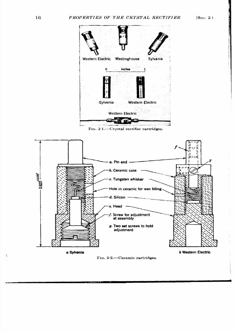
conven ience be called the “ceramic, ” or lN21-type, ca r t r idge.
Th e
ceramic ca t r idges of th ree manufactu rers a re shown at the top of Fig.
2.1.
The “coaxia l,”
or lN26-t ype, ca r t r idge was developed at the Bell
Telephone Labora tor ies for use in the l-cm region. It is more compact
than the ceramic ca r t r idge and is designed to match a coaxia l line having
a 65-ohm cha ra ct er ist ic impedan ce.
Th e coa xia l ca rt r idge has a lso been
used for the 1N31 type, which is a video crysta l for use in the 3-cm band.
The Western Elect r ic and Sylvania coaxia l a r t r idges re sho n in the
cen ter of Fig. 2. ~.
Th e pigta il ca rt ridge shown a t th e bot tom of Fig. 2“1 has been design ed
b Bell Teleph on e La bora tor ies for t he high in ver se-volta ge r ect ifier for
s econd-det ect or a nd ot h er d iode applica tion s.
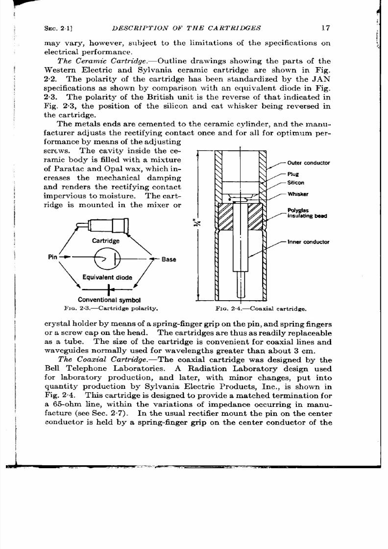
2.1. Descr ipt ion of the Car t r idges.-The externa l geomet ry o the
ca r t r idges has, except for the pigta il ca r t r idge, been standardized by the
J AN specifica t ions. Deta iled drawings showing the dimensions and
tolerances a re given in Appendix D. The deta ils of the ca r t r idge par ts
1Her einafterabbreviated “J AN.”
15
—
16
PROPERTIES OF THE CRYS TAL RECTIFIER
[sm. 21
—,
( ‘--v@
Western Electric Westinghouse
Sylvania ,
0
Inches
1
H!!ll
?
Sylvania
Western Electric
Western Electric
FIG. 2 1.—Crys ta l rect i fier car t r idges.
a Sylvania bWesternElectric
F IG. 22.-Cer amic ca r tr id ge
I
SEC.21]
may vary,
DESCR IPT ION 011’T HE CAR TR IDGES
17
owever , subject to the limita t ions of the specificat ions on
electrical performan ce.
The Ceramic Car tr idge. —Outlinedrawings showing the par ts of the
~
Western Elect r ic and Sylvania ceramic car t r idge are shown in Fig.
2.2. The polar ity of the car t r idge has been standardized by the JAN
specifica t ions as shown by compar ison with an equivalent diode in Fig.
2.3. The polarit of the Brit ish unit is the reverse of tha t indicated in
Fig. 2.3, the posit ion of the silicon and cat whisker being reversed in
the car t r idge .
The meta ls en s are cemen ted to the ceramic cylinder , and the manu-
facturer adjusts the rect ifying contact once and for all for opt imum per-
forma nce by mea ns of t he a dju st in g
scrc.ws. The cavity inside the ce-
ramic body is filled with a mixture
of Para tac and Opal wax, which in-
creases the mechanical damping
and renders th e rect ifying contact
,
I
imperviou s t o moist u re.
Th e ca rt -
r idge is mounted in the mixer or
[
I
Pin
~
Caftridge
— + Base
/
\
Equivalent diode
1=
/
Conventional symbol
FIG. 2.3.—Cartridge polarity.
Outerconductor
Plug
silicon
Whisker
Polyglas
insulatingbead
Inner conductor
FIG. 2.4.—Coaxial cart ridge.
cr yst al h older by mea ns of spr in g-fin ger gr ip on t he pin , a nd spr in g fin ger s
or a screw capon the head. The car t r idges are thus as readily replaceable
as a tube. The siz of the car t r idge is convenient for coaxial lines and
waveguides normally used for wavelengths grea ter than about 3 cm.
T he Coaxial Cartrid ge.—Th e
coaxia l car t r idge was designed by the
Bell Telephone La ora tor ies. A Radiat ion abora tory design used
for laboratory product ion , and la ter , with minor changes, put in to
quantity produ t ion by Sylvania Elect r ic Products, Inc., is shown in
Fig. 24. This car tr idge is designed to provide a matched terminat ion for
~
a 65-ohm line, within the var ia t ions of impedance occurr ing in manu-
facture (see Sec. 2.7). In the usual rect ifier mount the pin on the cen ter
k
conductor is held by a spring-finger gr ip on the cen ter conductor of the
i

18
PROPERTIES OF THE CRYSTAL RECTIFIER
[SEC. 22
ca rt ridge r ecept acle, a nd t he ou ter con du ct or is pr essed a ga inst a sh ou lder
on the ou ter conductor of the receptacle. 1
The ca t -wh isker and center -conductor assembly is moun ted on a
molded insula t ing bea d of polyglas tha t is pressed in to th e ou ter cylinder
and secu red by a cr imp in the ou ter conductor .
Th e cocficicn t of expa n-
sion of the polyglas bead matches tha t of the brass ou ter conductor and
thus pr ovides good stability un der condit ion s of changing t empera tu re.
The necessity of r igid const ruct ion is clear from the fact tha t the cylin-
dr ica l ca vit y con ta in in g wh isk er a nd cr yst al is a bou t 0.050 in . on g.
The silicon crysta l is soldered to a br ss plug pressed in to the end of
the cylinder . Adjustment of the rect ifying con tact is made by slowly
advancing the plug by means of a jig ca r rying a micrometer screw. The
cavity conta in ing the whisker and crysta l is, as in the ceramic car t r idge,
filled wit h wa x.
The Pigt ail Ca rt ridge.—Th e pigt ail ca rt ridge is design ed t o be solder ed
in place as a circu it elemen t. In t he pr esen t Bell Telephone Labora tor ies
design the head of the car t r idge is replaced by a st ructure similar to the
pin end. The rysta l is mounted, like the whisker , on a sliding rod held
by set screws af ter adjustment . The pigta il wires are mounted on fit t ings
pressed on to the pins after assembly and adjustment of the car t r idge.
The present form of th is ca r t r idge is not necessar ily the best one, but it
was adopted because of lack of t ime to develop a bet t er one.
It i likely
tha t an improved design will soon super sede it .
2.2. Stability and Handling Precaut ions.—These crysta l car tr idges
have a stability comparable to tha t of other circu it component s. Ca r t -
r idges stored under t ropica l as well as normal condit ions show no deter i-
ora tion with t ime. The J AN specifica t ions pr ovide for a ser ies of r igorous
mechanica l-design test s to insure long life under condit ions tha t exist in
actua l applica t ions and dur ing handling. These design test s provide
tha t the elect r ica l per formance sha ll not be impaired more than a small
specified amou nt a ft er bein g su bject ed t o t he followin g t rea tm en t:
1.
2.
3.
4.
5.
Immersion in a wa ter ba th a t 40”C for 15 min followed by immer-
sion for 15 t in in wa te a t 25”C.
A ser ies of t empera tu re cycles between the limits of –40”C and
+70”C. (Specifica t ions for some of t he video crysta l t ypes impose
limits of – 55°C and +85”C. The number of cycles specified
va r ies from type to type.)
A 30-in . drop on to a ha rdwood sur face. (Some of the video crysta l
t ypes specify a lWln. drop.)
Applica tion of a t or qu e of 1.5 in -lb a bou t t he ca rt ridge axis.
An axia l-st ra in test , consist ing of the applica t ion of a force of 1 lb
1See Chap. 9 for a more comple ted iscussion .
f
iiEC.
2.2] S TABILITY AND HANDLING PRECAUTIONS
19
applied a t the t ip of the pin a t r igh t angles to the car t r idge axis,
t he head of he ca r t r idge being held in a clamp.
The last two test s a re obviously not applicable to a ca r t r idge of the
coaxia l type.
The cr yst al r ect ifier may be impaired in per for ma nce in applica t ions
where it is requir ed to dissipa te excessive amounts of power .
This
p henomenon is ca lled “bu r nou t .”
In a rada r system using the same antenna for t ransmission and recep-
t ion , a TR switch’ is used to protect the rect ifier from the high -level
power of t he t ra nsm it ted pu lse.
The TR swit ch is a resonant cavity with
loops o ir ises for coupling r -f power in and ou t and conta ins a gas-filled
TR tube tha t is normally nonconduct ing. Cryst a l prot ect ion is ach ieved
by a gaseous discha rge in the TR tube in it ia ted by the t ransmit ted pu lse.
The ignit ion takes place in a t ime tha t is shor t compared with the pulse
length and provides an effect ive shor t circu it a t t he input termina ls of
the cryst a l mixer . The r -f power t r ansmit ted through the TR switch
dur ing the passage of a t r ansmit t ed pu lse will consist of a “ spike, ” ~vhich
is t ra nsmit t ed dur ing t he preignit ion t ime, followed by “ lea kage power , ”
which last s for t he rema inder of t he pulse.
The TR swit ch is designed t o
m in im ize bot h t hese effect s.
Dur ing the cour se of the war improvemen t s in TR tubes and associ-
a ted circu it s and in the resist ance to burnou t f cryst a l r ect ifier s made
possible a sa tisfa ct or y cr yst al life in du plexin g syst em s; t he life is limit ed
lar gely by event ua l TR-tu be fa ilure or th e fa ilu re of a ssoc a ted circu it s.
To insure adequa te resistance t o burnou t , t he J AN specifica t ions on th
mixer types call for bu rnout proof t est sz on each rect ifier .
Some of the
types, in addit ion , ca ll for a somewha t more r igorous burnout design test
on a small fr act ion of t he pr odu ct ion .
Th e t est s a r e su fficien tly r igor ou s
to insure a long life, comparable to tha t of conven t iona l vacuum tubes,
when the rect ifier is proper ly protect ed by a TR swit ch .
Exper ience has shown tha t crysta l r ect ifier s may be burned ou t by
improper handling or storage.
The discha rge of sta t ic elect r icit y
th rough the rect ifier , st a t ic elect r icity tha t may have accumula ted on
ungrounded appara tus or on the opera tor ’s body, is su fficien t to impair
ser iou s y t he m icr owa ve per forma nce of t he r ect ifier .
Damage may also
be incur red by a discharg to ground through the rect ifier when it is
in ser t ed in equipmen t ha t is opera t ing a t other than ground potent ia l.
Damage of th is sor t may easily be avoided by grounding the appara tus
and by holding the ca r t r idge by the base and making bodily con tact with
t he equ ipm en t ju st befor e in ser tin g t he ca rt ridge.
1See J i’tcrounveDup lezers ,1’o1.4, RadiationLabora torySeries,for a full discussion.
i A “proof t es t ” s l]ou ldnot be confusedwith a “des ign tes t ,” The formermerely
culls the unit s with poor burnout character is t ics .
20
to
PROPERTIES OF THE CRYSTAL RECTIFIER
[SEC. 23
The cryst al r ect ifier ma y also be dam aged by exposur e of t he ca rt ridge
intense r-f fields in the neighborhood of high-power t r nsmit t ing
systems. The manufacturers provide meta l conta iners for stor ing the
car t r idges when not in use. One convenient type of conta iner is a lead
capsule which can be slipped over the car t r idge. This precaut ion is
obviously ot necessa ry for t he coaxia l ca r t r idge, which is effect ively
shield d by the ou t er conductor ; th is design also minimizes the danger of
damage by elect rost at ic disch ar ge.
ELECTRICALPROPERTIES
2.3. Th e Volt age-cu rr en t Ch ar act er ist ic.—Th e st at ic r ect ifier ch ar ac-
ter ist ic is of in terest on severa l counts. It is obviously of importance in
the t heory of point -contact rect ifica t ion in tha t an adequa te t heory must
pr edict qu an tit at ively t he fea tu res of t he cu rr en t-volt age ch ar act er ist ic.
In t he second pla ce it has a lrea dy been point ed out t hat for low-fr equency
+20
+15
F
c
“: +10
:
3
~ +5
G_
%?
‘O
-5
-2.0 -1.5 -1.0 - .5 0 +0.5 +1.0
Appkdvoltage
F IG. 25.-A t j-pica l ch :lr act er ist ic cu r~-c
of a sdicon Icr t ilicr .
det ect ion a h igh ba ck r esist an ce a nd
h igh forwa rd conduct a nce, t oget h er
with a sha rp cur va ture a t t he or igin,
a re desirable. Finally in the man-
u fa ct u re of r ect ifier s for m icr owave
use, it is common pra t ice t o use t he
st at ic ch ar act er ist ic a s a cr it er ion or
guide for the adjustment of the rec-
t ifying contact . It should be em-
phasized, hotvcver , that a good
sta t ic character ist ic is not a suffi-
cien t condit ion for a good micro-
wave performaucc.
At sufficiently
hl~h frcqucmcics the shunt ing ef-
fect of the capacit ance of the barr ier a ; t he r&ifying con tact bcc~mes
important . For this reason t he size of t he contact a rea must be cont rolled.
J lor eover , in m icrowa ve a pplica t ions ot her fa ct ors, such as noise and im-
pedance, a re of importance. The measllrcmcnt of such high-frequency
proper t ies is t herefore also specified in a product ion test of t he standard
t ypes t o en su re sa tisfa ct or y a nd u niform per forma nce.
A typica l character ist ic curve of a silicon rect ifier unit is shown in
Fig. 2.5. The cur ren t increases exponent ia lly in the for lva rd direct ion
for a few tenths of a volt . As the current increases fu r ther , t he curve
approaches a st ra ight line whose slope is determined by the spreading
r esist an ce (see Sec. 2.4 a nd Ch ap. 4) in t he sem icon du ct or .
The for lva rd
cur ren t a t 1 volt is 10 to 20 ma for a good mixer crysta l.
In the back direct ion a high-resistance rc~ion for voltages of a felv
volt s is followed by a region where the clu-rent increases rapidl~r ~vith

THE VOLTAGE-CURREN T CHARACT ERIS TIC
21
EC. 2.3]
further
increase in nega t ive volt age, so rapidly in some cases tha t it
a ppr oa ch es a n expon en tia l beh avior .
Thestandardrnixer crysta l types
have at 1 volt a back resistance of approximately 5000 to 10,000 ohms.
The character ist ic curvesin the forward direct ion of severa l typica l
r ect ifie s a re shown in la rger sca le for compar ison purposes in Fig. 2.6.
It is to be noted tha t the’’ break”
in the character ist ic of the crysta l
r ect ifier s is much mor e p ronounced
than that of thevacuu tube and
the forward conductance at abou
0.5 volt or more is much la rger .
Th e sma ller cu rr en ts obt ain ed wit h
germ an ium, a scon tr ast ed w t h sili-
con , a t a few ten ths of a volt is
typical.
Ch ar act er ist ic cu r ve B (F ig. 26)
is t ypica l of t he welded-con ta ct r ec-
t ifier developed r ecen tly by N ’or th ’
a t the Genera l Elect r ic Company.
Th ese u nit s u se germanium cr yst als
con ta in in g 0.2 a tom ic per cen t a nti-
mony. The whisker is welded to
the crysta l by the passage of 250 ma
of direct cu r en t fora shor t t ime in
the forward direct ion . The diam-
8
A Silicon
7 -
B Germaniumwelded
contact
C . Germaniumhigh.
inversevoltage
6
D .6AL5vacuum.tube
d!ode
?5 -
~
F
:
24
“
;
=3
:
2 -
1 -
0
0
0.1 02 03
0.4 0,5 0.6
Voltage
n the forwarddirection in volts
F IG. 26.-A compa r ison of t he ch ar a ct er is-
t ic curves of severa l rect ifie rs.
et er of the weld on a typica l whisker is approximately 0.0002 in . The
expon en tia l r egion of t he ch ar act er ist ic is u nu su ally la rge compa red wit h
ot h er r ect ifier s, a ndin th e for \ ~a r d dir ect ion it t her efor e appr oa ch es closely
t he idea lz d -c cha r act er is tic,
~ = ~(e.E
– 1),
(1)
where i is the direct cur ren t , A and a are constan ts, and E is t he volt age
across the barr ier . Thevolt age Eis given by
E= E’–ir,
(2)
where E’ is t he voltage applied to the rect ifier and r is the spreading
resistance in the semiconduc or a t the con tact poin t .
F igu re 2.7 sh ows
the logar ithmic character ist ic of a typica l unit , as observed by Tor rey. ?
It sh ould be n ot ed tha t t he coordin ates a re .sem ilogar ithmic; h en ce a plot
1H. Q. Nor th , F iu al Repor t ,
“VJ elded GermaniumCrystals,” Cont ract OEMsr-
262, Order No DIC-178554, Sep t. 20, 1945. (Th is workwm done a t t h e Resea r ch
Laboratoryof the GeneralElectr icCo.)
2SeeChap. 4 for a discussionof the theory of the ideal d-c char acteristic.
*H. C. Torrey, unpublisheddata a t RL.

22
PROPERTIES OF THE CRYSTAL RECTIFIER
[SEC. 2.3
of Eq. (1) would follow a st ra ight line for appreciab e values of E’.
From Torrey’s curve the following values for the constant s of Eq. (1)
were obta ined :
A = 0.0035 pa
o. = 29.8
per volt
r = .2
ohms.
These rect ifiers a re unique in having an abnormally low va lue of the
100,OOC
10,OOC
m
= 1,000
.5
z
g
~
u
*9
.=
g 100
m
10
1
1-
0(
I
0.4
0.6
-iR8
/
/
l’IG. 27.-Loear ithn1ic character is t ic of
a germanium
welded-contact
rect]fier.
P oin ts on t he br oken cu rve a re ca lcu la ted
for a spr eading r es is ta nce o 3.2 ohms.
spreading resist ance and a chara c-
ter ist ic which is accurately expo-
n ent ia l for forwa rd cu rr en ts as high
as 10 ma.
Th e cu rr en t-volt age ch ar act er -
ist ic of a typical germanium high-
inverse-voltage rect ifier made at
Purdue University is shown in Fig.
2.8. The forward current a t 1 volt
or this par t icular unit is 8 ma
The crysta l in this unit ~vas made
fr om an a lloy con ta in in g 0.25 a tom -
ic per cent of t in.
Outstanding fea tures of the
character ist c curve are the high
value of the peak back voltage and
the nega t ive resist ance re ion ex-
hibit ed in t he ba ck dir ect ion for cur -
rent s exceeding the curren t a t t he
peak back voltage. This curve is
cliscussed in much more cleta il in
hap. 12. Recen t ly Thcwerer and
Scaffl ha ve developed a pr ocedu re
for the heat t rea tment of ingot s of
germani urn
a lloyed with 0.1 pm
cent t in;
ingots a rc obta ined in
vhich all but thcllppcr third of the
in got pr odu ces r ect ifier s ~~it h pea k
inverse voltages \ vith in a range
gr ea ter tha 50~olts a ndeven approaching 200volts. In thcbackdirec-
t ion a t a bout 30 volt s t hese r ect ifier s ha ve resist ances r an ging r om 10,000
ohms to more than 1 megohrn.
The forward cur rent s a t 1 volt lie in the range from 5 to 10 ma, an~l
lH. C. Theuerer and J . H. Staff,
“Hea t Trea tment of Germanium Rect if er
Nfaterials,
NTDRC14-506, Contra ct OEhfsr-1408, Bell Telephone I,aboratories,
Aug 3, 1945.
— ——..
i3Ec.2.4]
THE EQUIVALENT CIRCUIT 23
cu rren ts grea ter than 100 ma may be passed in the forward direct ion
wit hou t impa ir in g t he r ect ifyin g con ta ct .
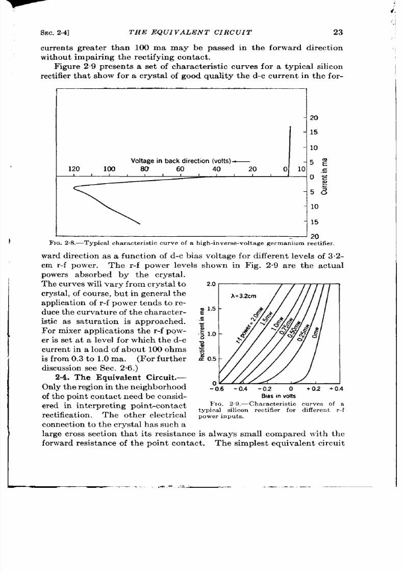
F igure 2.9 present sa set of cha rac er ist ic cu rves fora typica l silicon
rect ifier tha t sh w for a crysta l of good quality the d-c cu rren t in the for -
1
!
Volta~e in back direction (volts)—
I
120 100 S6
60 40 20 (
t
I ,
1
I
0
15
j ,0
FIQ.2+3.—Typical character is t ic curve of a high-inverse-voltage germanium rect ifier ,
wa rd dir ect ion as a fun ct ion of d-c bias volt age f r differ en t levels of 3.2-
cm r-f power . The r-f power levels shown-in Fig. 2.9 a re the actua l
powers absorbed by the crysta l.
Th e cu rves will va ry from crysta l t o
2.0
cr yst al, of cou rse, bu t in gen er al t he
a pplica t ion of r -f power ten ds t o r e-
m 1.5
du ce t he cu rva tu re of t he ch ar act er - E
ist ic as sa tura t ion is approached. ~
Formixer applica t ions ther -f pow- .~l,o
er is set a t a level forwhich the d-c ~
cur ren t in a oad of about 100 ohms E
is from 0.3 to 1.0 ma. (For fu r ther I 0.5
d iscu ss ion see Sec. 2.6.)
2.4. Th e Equ ivalen t Circu it .—
Only the r egion in t he neighborhood
-00.6 -0.4
-0.2 0
+0.2 +(
of t he poin t con ta ct n eed be con sid-
Bias in volts
er ed in in ter pr et in g poin t-con ta ct
FIG. 29.-Character ist ic cu rves of a
t ypical silico r ect ifier for differ en t r -f
rectification. The other elect r ica l
powerinputs.
i.
‘ i
con nect ion t o th e crysta l has such a
la rge cross sect ion tha t it s resistance i a lways sma l compared with the
forwa rd r esist an ce of t he poin t con ta ct .
Th e simplest equ iva len t cir cu it
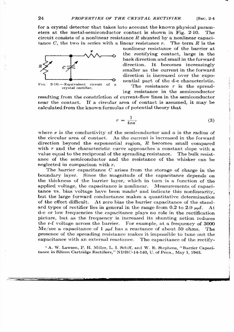
.-
24
PROPERTIES OF THE CRYSTAL RECTIFIER
[SEC.
2.4
for a crysta l detector tha t t akes in to accoun t the known physica l pa ram-
eter s a t the meta l-semiconductor con tact is shown in Fig 2.10. he
cir cu it con sist s of a n on lin ea r r esist an ce R sh un ted by a nonlin ea r ca paci-
t ance C, the two in ser ies with a linear resistance r . The term
R
is the
non linear resist ance of t e ba r r ier a t
the rect ifying con tact , la rge in the
‘c’rec’iOn”l’becOmesincreasingly
ba ck dir ect ion a nd sm all in t he forwa rd
smaller as the cur ren t m the forw rd
direct ion is increased over the expo-
n en tia l pa rt of t he d-c ch ar acter ist ic.
FIG.
2.10.—Equivalent circu it of a
crystal rectifier.
The resistance r is the spread-
ing resistance in the semiconductor
r esu lt in g fr om t he con st rict ion of cu rr en t-flow lin es in t he sem icon du ct or
nea r the con tact . If a circular a rea of con tact is assumed, it may be
calcula ted fr om t he kn own form ula s cf potent ia l t heor y th at
(3)
where u is th e conduct ivi y of the semiconductor and a is the radius f
the circu la r a rea of con tact . As the cu rren t is increased in the forward
direct ion beyond the exponen t ia l r egion , R becom es small com pa red
with r and the character ist ic cu rve approaches a constan t slope with a
va lu e equ al t o t he r ecipr oca l of t he spr ea d n g r esist an ce.
Th e bu lk r esist -
ance of the semiconductor and the resist ance of the whisker can be
neglected in compar ison with r .
The bar r ier capacitance C ar ises from the storage of cha rge in the
boundary layer . Since the mag itude of the capacitance depends on
the th ickness of the ba rr ier layer , wh ich in tu rn is a funct ion of the
a pplied volt age, t he ca pa cit an ce is n on lin ea r.
Mea su remen ts of ca pa ci-
tance vs. bias voltage have been madel and indica te th is non linear ity,
but the la rge forwa rd conductance makes a quan t ita t ive determina t ion
of the effect difficu lt . At zero bias the ba r r ier capacitance of the stand-
ard types of rect ifier lies in genera l in the range from 0.2 to 2.0 ypf. At
d-c or low frequencies the capacitance plays no role in the rect ifica t ion
pictu re, but as the frequency is increase it s shun t ing act ion reduces
the r-f voltage across the ba rr ier . For example, a t a frequency of 3000
Me/see a capacitance of 1 y&f has a reactance of abou t 50 ohms. The
presence of the spreading resist ance makes it impossible t o tune ou t th e
capacitance with an externa l reactance. The capacitance of the rect ify-
I A. W. Lawson, P. H. Miller , L. 1, S hiff, an d W. E. Stephens, “Bar rier Capaci-
t a nce in S ilicon Ca r tr idge Rect ifier s, ”
NDRC-14-140, U . of P en n., Ma y 1, 1943.
!
I
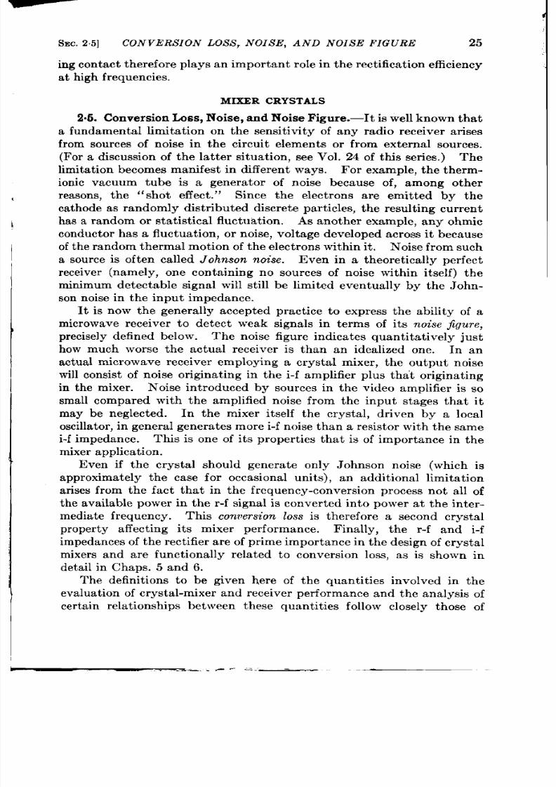
SEC.25]
CONVERS ION LOSS , NOIS E, AND NOISE FIGURE
25
in g con ta ct t h er efor e pla ys a n impor ta nt r ole in t he r ect ifica tion efficien cy
a t h igh frequencies .
MIXER CRYSTALS
2.6. Con version Loss, Noise, a nd Noise Figur e.—It is well known t hat
a fundamenta l limita t ion on the sensit ivity of any radio receiver a rises
from sources of noise in the circuit elements or from externa l sources.
(For a discussion of the la t t er situa t ion, see Vol. 24 of this ser ies.) The
limita t ion becomes manifest in different ways. For example, the therm-
ion c vacuum tube is a genera tor of noise because of, among other
reasons, t he “shot effect . ”
Since the elect rons a re emit t ed by the
ca thode as randomly dist r ibuted discret e pa rt icles, t he result ing cu rren t
h as a r an dom or st at ist ica l flu ct ua tion .
As another example, any ohmic
con du ct or a s a fluct ua tion , or n oise, volt age developed a cr oss it beca use
of t he ra ndom t herma l m ot ion of t he elect ron s within it .
Noise fr om su ch
a source is often ca lled J o nson nm”se. Even in a theoret ica lly per fect
receiver (namely, one conta in ing no sources of noise within itself) the
minimum detect able signal will st ill be limited eventua lly by the J ohn-
son noise in t he input impeda nce.
It is now the genera lly accepted pract ice to express the ability of a
microwave receiver t o detect weak signals in terms of its noise jigure,
precisely defined below. The noise figure indica tes quant it a t ively just
how much worse the actual receiver is than a idea lized one. In an
actual microwave receiver employing a crysta l mixer , the outpu noise
will con sist of n oise or igina ting in t he i-f amplifier plus t ha ’t or igin at in g
i the mixer . Noise in t roduced by sources in the video amplifier is so
small compared with the amplified noise from the input stages that it
may be neglected. In the mixer it self the crysta l, dr iven by a local
oscilla tor , in gen er al gen er at es mor e i-f n oise t ha n a r esist or wit h t he same
i-f impedance. This is one of it s proper t ies tha t is of importance in the
mixer applicat ion.
Even if the crysta l should genera te only J ohnson noise (which is
approximately the case for occasional units), an addit ional limita t ion
ar ises from the fact that in the frequency-conversion process not a ll of
t he available power in the r -f signa l is conver ted into power a t the in ter -
media te frequency. This conversion loss is therefore a second crysta l
proper t y affect ing its mixer performance. Finally, t he r-f and i-f
im peda nces of t he r ect ifier a re of pr im e impor ta nce in t he design of cr y t al
mixers and are funct ionally rela ted to conversion loss, as is shown in
deta il in Chaps. 5 and 6.
The definit ions to be given here of the quant it ies involved in the
evalua tion of cryst al-mixer and r eceiver per form ance and t he analysis of
cer ta in rela t ionships between these quant it ies follow closely those of

26
PROPERTIES OF THE CRYSTAL RECTIFIER
[SEC.2.5
Friis, 1 a nd Rober t s, 2 th e la t ter in t roduc n g t he con cept of effect ive noise
figure.
First will be considered any four-termina l network connected to J
signal genera tor and an ou tpu t circu it as shown in the block diagram of
Fig. 2.11. The input and ou tpu t impedances of the network may have
Signal
Four4erminal
output
r eact ive componen ts and may or may
generator
network
circuit
not be matched to the genera tor and
ou tpu t cir cu it s.
o
Gain of the Network .—The sign al
-cl c- —
4
genera tor may be rega rded as a volt -
FIG.2.1 l.—Block diagram for the ana ly-
age source E in ser ies with an imped-
s is of the network noise figu re.
an te R + jX. To get the maximum
power in to a load, the load should have an impedance R – jX. This
maximum power is by defin it ion the available power from the signal
gen era tor , and is given by th e expression
(4)
Similar ly, the ou tpu t terminals of the network can be t rea ted as a
new source of signal, having an available power output , wh ich will be
ca lled S’,. The power gain G of the network is defined by the rela t ionship
(5)
The gain is by de init ion independen t of the impedance presen ted to the
network by the ou tpu t circu it but is a funct ion of the genera tor imped-
ance. It is apparen t tha t for some part icu lar genera tor impedance the
power gain will be a maximum, which will be called G~. Another usefu l
defin it ion of gain especia lly a pt for a crysta l mixer is obta in ed by match-
in g a signal gen er at or to t he cr yst al m ixer a t loca l-oscilla tor fr equ en cy.
This gain wil be denoted by Go.
.
Tie “loss” of a network is, of course, the reciproca l of the power gain .
The term is often used instead of “ ga n” wh n the network is a crysta l
mixer , a situa t ion in which one is a lmost invar iably concerned with con-
ver sion ga ins less t ha n u nit y.
Noise F igu re.—For m akin g m ea su rem en ts of n oise power , a pra ct ica l
standard of compa rison is t he J ohnson noise gener ated in a r esistor .
available n oise power from a r esist or in to a “ cold, ” or noiseless, load in an
in cr emen ta l ba nd of fr equ en cy d f is given by t he well-kn own expr ession
dN = kYdf,
(6)
1H. T. Fr iis , “ Rcceivcr Noise Figures,” IITL Memorandum hfM-42-16@39,
Ma y 13, 1942; P roc. I. R. E ., S2, 419 (1944).
z S , Rober t s,
“Th eor y ‘of Noise Nlca su rcm en ts on (;r ysta ls as F requ en cy Con -
ver ter s,” RL Repor t No. 61-11, J an . 30, 1943,
SEC.2.5]
where k is
CONVERS ION LOSS , NOISE, AND NOISE FIGURE
27
Boltznumn’s constan t , N is the available noise power , and T
is t he a bsolu te t emper at ur e.
It is conven ien t to choose as a standard
temperature To = 290°K, in ~vhich cfise kT = 4 X 10–~’ jou le, and
kT / ej a not her qu an tit y fr equ en tly cn count er edj is 0.025 volt .
In so fa r as noise considera t ions are concerned, a per fect net \ vork is
on e wh er e t her e a re n o n oise sou rces ]r it hin t he n et ivor k it self.
Actually,
such networks exist ; in such a case the ra t io dN[)/So of available ou t -
pu t n oise po!ver t o a~’ailable ou tpu t signal polver is gr ea ter than t he r at io
dN / S of available inpu t noise pofver o available input signal power .
The noise figure F of the net \ vork is then defined for this book by the
equation
dN,
= ~,,k l’, df,
so s
(7)
in wh ich kTO df is t he available inpu t n oise power fr om a r esistor .
From
Eqs. (5) and (7) \ ve obta in
dNo = FGkTO df.
(8)
The no se output , noise figure, and the gain are alike in tha t all a re func-
t ions of the impedance of the genera tor . The noise figure is a minimum
for som e pa rt icu lar valu e of gen er at or impeda nce, wh ich in gen er al is n ot
the same as that giving maximum gain .
E flectiv e Noise Figure.—In actual pract ice networks that have fin ite
bandwid hs are of concern . The tota l available noise ou tpu t of such a
network is given by the in tegral of Eq. (8),
No = kTo
/
“ FG df. (9)
o
Now Eq. (7) can be rewr it ten in the form
dNo
dN
— = FG,
(lo)
fr om wh ich it is seen t hat FG is a t least as gr ea t as u nity at all fr equ en cies,
and the integral in 13q. (9) ther efore does not converge.
Actu ally in
making measurements of ou tpu t noise some form of wat tmeter which
measures the amoun of power delivered in to some load is used. This
quant ity will dr op t o zer o outside the pass band of the amplifier , wh ereas
t he available J oh nson -noise power at t he ou tpu t terminals of t he n et wor k
is independen t of frequency. In t rea t ing effect ive noise figure the ou t -
pu t-m et er gain is in tr odu ced an d defin ed as t he r at io of t he pow r actua lly
delivered in to the meter to the power available from the network. In
Eq. (9), G then is define as the gain of the network-ou tpu t -meter c m-
binat ion, and is the product of the power gai of the amplifier and tha t of
the ou tpu t meter . The in tegra l in Eq. (9) then converges.

28
PROPERTIES OF THE CRYSTAL RECTIFIER
[s1;(.3
‘l’h e effect ive n oise figu re F ’ is n ow defin ed b t he r ela ti m
(11)
where N; is the available ou tpu t noise po\ ver if F \ vcrc un ity a t a ll fr e-
qu en cies, t ha t is,
r .
(12)
In other words Nj is the noise tha t w-ou ld be delivmcd to the ou tpu t load
if t her e wer e n o n oise sou rces \ vith in th e n etwor k.
The effect ive nois e figu r e F’ is t hen given by t he expr ession
/
- FG df
~r=m= o
N ; - “
J
G df
o
(13)
The effect ive, or nois e, bandwid th B of th e n et wor k can n ow be defin ed
as
/
cc
G df
B= ‘G ,
(14)
ma.
wh er e G-. is t he m aximum of t he pot ver ga in vs. fr equ en cy ch ar act er ist ic.
In t roducing Eq. (14) in to Eq. (13), we obta in for the effect ive noise
figu r e t he exp res sion
F, =
No
kTOBG_’
(15)
wh ich gives F’ in t erms of measurable quan tit ies.
The applica t ion of
Eq. (15) in the measurement of receiver noise figure is discussed in
Chap. 7.
Signal * —
‘Networl?
aNetworkO 0 output
generator ~
o
1
0- - -J
2
0- -.— -0
circuit
4
FIG. 2 .12.—Two networks in cascade.
Noise F gure of Two Networks in Cascade.—The noise figure for
two networks in cascade, shown schemat ica lly in Fig. 2.12, can now be
obta ined in terms of the proper t ies of the two networks.
Applying Eq, (8) to the two networks as a whole, we obta in for the
noise out u t in the incrementa l frequency band d f t he expression
dN o(l+zj = Fl+zGwzk7’o Ly,
(16)
where the subscr ipt (1 + 2) indica tes tha t the quant ity applies to the
I
I
I

—— . . .
SEC.25]
CONVERS ION LOS S , NOISE, AND NOIS E FIGURE
29
over -a ll n et wor k. Th e rela t ion ,
follows direct ly from the defin it ion of ga in . From Eqs. (16) and (17)
we obta in
dN oc,~,) = F,~2G,G2kTo dj.
(18)
Simila r ly, Eq. (8), applied t o n et wor k 1, gives
dN,, = F,GJ cTO dj. (19)
The pa r t of the outpu t noise from network 2 or igina t ing in t he signa l
genera tor and network 1 is
dN ;(,~,> = dNo,G, = F,G,GzkTo dj.
(20)
The pa r t of the ou tpu t noise from network 2 or igina t ing with in network
2 is
dN:[,~,) = F,G,kTo dj – G2kT0 dj.
(21)
The se ond term of the r igh t -hand member of Eq. (21) is subt racted in
order not to include for a second t ime the J ohnson noise from the ou tput
r esist an ce of n et w r k 1.
The addit ion of Eqs. (20) and (21) gives for the tota l outpu t noise
powe r t h e exp res sion
dN,(l+,) = dN ;(l+z) + dW(l+z)
= F,G,G,kTo dj + F,G,kTo dj – G,kT , d f.
(22)
Equat ing the r igh t -hand members of Eqs. (18) and (22), we obta in
(23)
Put t ing Eqs. (23) nd (17) in to Eq. (13), we have for the effect ive
noise figure
/
.
G,G,F, + G,(F, – 1) df
F:l+z) = 0 ~
\
(24)
G,G, dj
o
If network 2 has a small bandwidth compared with network 1, G, and
FI may be considered constan t over the range of in tegra t ion ; in th is case
Eq. (24) reduces to
Fi~2
F;–1
‘F’+
G, “
(25)
In per forming the in t egra t ion indica ted in Eq. (24), t he factor Gz
in the t erm G,(FZ — 1) is to be rega rded as the gain f the network-meter
.-—
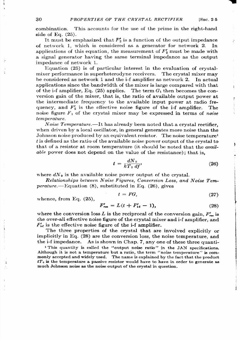
.-—
30
PROPERTIES OF THE CRYSTAL RECTI IER
combinat ion . This a coun t s for the use of the pr ime in the
side of Eq. (25).
It must be emphasized tha t F; is a funct ion of the ou tpu t
[SEC. 25
right-hand
impedance
of network 1, which is considered as a genera tor for network 2. In
applica t ions of th is equa t ion , the measurem nt of F; must be made with
a signal genera tor having the same terminal impedance as the ou tpu t
impedance of network 1.
Equa t ion (25) is of par t icu lar in terest in the eva lua t ion of crysta l-
mixer perform ance in su perheterodyn e receiver s. The crysta l mixer may
be considered as network 1 and the i-f amplifier as network 2. In actua l
applica t ions since the bandwidth of the mixer is la rge compared with that
of t he i-f amplifier , E q. (25) a pplies.
The term I then becomes the con-
ver sion gain of th e mixer , tha t is, th e ra t io of available o tpu t power a t
the in termedia te frequency to the ava ilable input power a t radio fre-
q ency, and F; is the effect ive noise figu re of the i-f amplifier . The
noise figure F1 of the crysta l mixer may be expressed in terms of noise
temperature.
Noise Tempera tu re.—It has a lrea dy been n oted tha t a crysta l r ect ifier ,
when dr iven by a loca l oscilla tor , in genera l gen era tes m ore noise than the
J oh nson n oise pr odu ced by an equ iva len t resist or . Th e n oise tem per at ur e
t is defined as the ra t io of the available noise power ou tpu t of th e crysta l to
tha t of a resistor a t room tempera tu re (it shou ld be noted tha t the avazl-
able
power does not depend on the va lue of the resistance); tha t is,
dNo
t = kT , d j’
(26)
where dNO is the available noise power ou tpu t of the crysta l.
Relationsh ips between Noise Figures, Conversion Loss, and Noise T em -
per atu re.—Equ at ion (8), su bst itu ted in Eq. (26), gives
t = FG,
(27)
wh en ce, from Eq. (25),
F;en = L(t + l’{, – 1),
(28)
wh er e t he con ver sion loss L is t he r eciproca l of th e con ver sion gain , F~= is
t he over -a ll effect ive n oise figu re of t he cr yst al m ixer a nd i-f amplifier , a nd
F{, is t he effect ive n oise figu re of th e i-f amplifier .
The th ree proper t ies of the crysta l tha t a re involved explicit ly or
implicit ly in Eq. (28) a re the conversion loss, the noise tem pera tu re, and
the i-f impedance. As is shown in Chap. 7, any one of these th ree quan ti-
1Th is qu an tit y is ca lled t he “ou tpu t n oise r at io” in t he JAN specifica tion s.
Alt h ough it is n ot a t emper a tu r ebu t a r a tio, t h e t erm “noise t emper a tu r e” is com-
monly acceptedand widelyused.
Th e n am e is expla in ed by t he fact th at t he pr odu ct
t TOis the t empera ture a passive resistor wou ld have to have in order to genera te as
m uch J oh nson n oise as t he n oice ou tpu t of t he cr yst al in qu est ion .
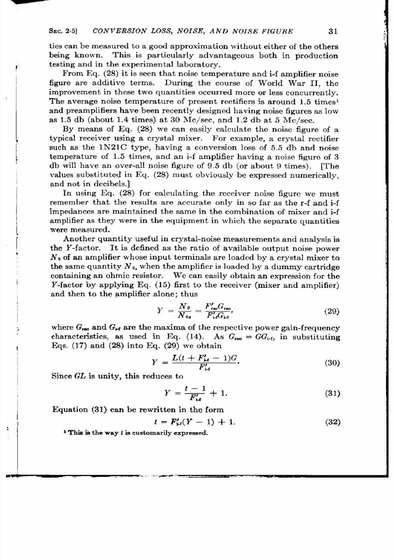
SEC.2.5]
CONVERS ION LOS S , NOISE, AND NOISE FIGURE
31
t ies can be measured to a good a proximat ion without either of the others
being known. This is par t icu lar ly advan tageous both in product ion
t est in g a nd in t he exper im en ta l la bor at or y.
From Eq. (28) it is seen tha t noise t empera tu re and i-f amplifier noise
figu re a re addit ive terms. Dur ing the cour se of Wor ld War II, t he
im pr ovem en t in t hese t wo qu an tit ies occu rr ed mor e or less con cu rr en tly
The average noise tempera tu re of presen t rect ifiers is a round 1.5 t imesl
a nd pr eamplifier s h ave been r ecen tly design ed h avin g n oise figu res a s low
as 1.5 db (about 1.4 t imes) a t 30 Me/see, and 1.2 db at 5 Me/see.
By means of Eq. (28) we can easily ca lcu la t e the noise figu re of a
t ypica l r eceiver using a crysta l mixer .
For example, a crysta l rect ifier
such as the 1N21C type, having a conversion loss of 5.5 db and noise
t empera tu re of 1.5 t imes, and an i-f amplifier having a noise figure of 3
db will have an over -a l noise figu re of 9.5 db (or about 9 t imes). [The
values subst itu ted in Eq. (28) must obviously be expr essed n umer ica lly,
a nd n ot in decibels.]
In using Eq. 28) for ca lcu la t ing the receiver noise figu re we must
r emember tha t the resu lt s a re accura te only in so far as the r -f and i-f
impedances a re main ta ined the same in the combina t ion of mi er and i-f
amplifier as they were in the equipment in which the sepa a te quant it ies
were measu red .
An ot her qu an tit y u sefu l in cr yst al-n oise mea su rem en ts a nd a nalysis is
the Y-factor . It is defined as the r t io of ava ilable outpu t noise power
NO of an amplifier whose inpu t termina ls a re loaded by a crysta l mixer to
t he same quant ity NO. wh en t he amplifier is loa ed by a dummy ca rt ridge
conta in ing an ohmic resistor . We can easily obta in an expression for the
Y-factor by applying Eq. (15) fir st t o the receiver (mixer and amplifier )
and then t o the amplifier a lone; thus
(29)
wh er e Gw a nd Gt i a re t he ma xima of t he r espect ive power ga in -fr equ en cy
cha racter ist ics, as used in Eq. (14). As Gm = GGi.f, in subst itu t ing
Eqs. (17) and (28) in to Eq. (29) we obta in
y = L(t +
1’:, –
l)G
~:< “
(30)
Since
GL is
unity, th is r educes to
Equat ion (31) can be rewr it t en in th form
t = F:,(Y – 1) +
1This ia
t h e way t is cu st oma rily exp res eed .
(31)
1. (32)

:
32
PROPERTIES OF THE CRYSTAL RECTIFIER
[SEC,2>
Equat ion (32) provides a convenient means of measuring noise t em per a-
ture in terms of the Y-factor and the noise figure of the i-f amplifier . In
actual pract ice ca re must be taken in the design of the amplifier input
ci cuit to insure that the Y-factor is independent of the i-f impedance
of the mixer over t he range o normally encountered crysta l i-f imped-
ances. Circuit s fulfilling this requirement a re discussed in Chap. 7.
Anot her useful rela t ionship can be der ived by t he combinat ion of Eqs.
(28) a nd (32):
F:ec = LF;., Y. (33)
Equat ion (33) is convenient t o use in the sta t ist ica l study of burnout in
tha t a measurement of conversion loss and Y-factor before and after
-1.0 1.5 2.0 2.5
3.0 3.5
Noisetem pera tu re
FIQ. 213.-Typica l dist r ibut ion of
noise t empera ture of 1N21B rect i iers.
Ra ndom sample select ed pr ior t o a ccept -
ance tes t s.
150-
.g l@J
s
50 -
0
4.5 5.5 6.5 7.5 8.5 >9.0
Conversionossmdb
FIG.2.14.—Typica l d is t r ibut ion of con-
ve r sion 10ss of 1N21B rect ifie rs .
Random
sample s elect ed p rior t o a ccep tance t es ts .
a pplica tion of specified amount s of power en ables on e t o ca lcu la te dir ect ly
the consequent impairment in receiver noise figure. The deter iora t ion
of r eceiver n oise figu re expr essed n decibels is ju st t he sum of t he det er io-
r at ion in Y-fa ct or a nd conver sion loss expr essed in decibels.
Range of Conversion Loss and N oise Tem perature in Production Unih.-
In the manufacture of crysta l rect ifier s, even by the most ca refully con-
t rolled met hods, a consider able spr ea d in t he va lu es of con ver sion loss a nd
noise tempera ture is found. ~igures 2.13 and 2.14 show typical dkt r ibu-
t ions of ra ndom samples t aken from t he manufact urers’ product ion lines
before reject ion of units failing to pass t e performance test s. These
units were t ype 1N21B rect ifier s for 10-cm use. Similar dist r ibut ions of
t he Radia t ion Labora tory rect ifier for l-cm applica t ions, typica l of the
1N26 type, a re shown in Figs. 2.15 and 2.16. These data were taken with
the standard test equipment descr ibed in deta il in Chap. 9, as prescr ibed
I
I
SEC.2.6]
OPTIMUM LOCAL-OS CILLATOR LEVEL
33
by t he JAN specificat ion s, wit h t he except ion of t he n oise t em per at ur es of
Fig. 2.15 wh ich wer e mea su red u sin g a r adio fr equ en cy of 24,000 Me/see
a nd a n in termedia te fr equ en cy of 60 Me/see.
(As indica t ed in ppendix
D, th e J AN specifica t ions provide for th e measurement of th e noise tem-
pera ture of type 1N26 rect ifie s at a radio frequency of 9375 Me/see.)
Summa rized briefly, t he t est condit ion s for t hese mea su remen ts con sist
of a mixer having a fixed r-f tuning, a specified i-f and d-c load, and a
specified r-f power level and r adio fr equ en cy. Th e d-c bias volt age is th at
due to the rect ified curren t in to the d-c load and is about – 0.1 volt .
Noisetemperatu~
F IG. 2.15.—T yp ica l d is tr ibu t ion of
n oise t emper at ur e of 1N26 r ect ifier s.
Random sample of unit s made at tbe
Radiation Laboratory.
2.6. Op timum Leca l-oscilla tor
15
n
“~10
5
Specification
*)
limit
Conversionossin db
F IG. 216.-Typ ica l d is tr ibu t ion of con -
ver sion loss of 1N26 r ect ifiers. Ra ndom
sample of unit s made at t he Radia t ion
Laboratory.
Level.—The conversion loss, noise
t emper a tu r e, and r eceiver nois e figu r e a r e a ll funct ion s of t h e loca l-’oscilla -
tor power level. F igure 2.17 shows the conversion loss and noise tem-
per at ur e of a t ypica l 1N23B r ect ifier (X = 3.2 cm) as a fu nct ion of r ect ified
cu rr en t; th ese cu rves a re obt ain ed by va ryin g t he loca l-oscilla tor power .
The curves a re a lso character ist ic of the other frequency bands. The
noise-t emper at ur e cu rve is a ppr oximat ely lin ea r over t h e r ange of in ter est .
The conversion loss approaches a constant va lue as the rect ified cur rent
is increased; above a rect ified curren t of approximately 1 ma there is
lit tle ch ange in conver sion loss.
Th e effect of loca l-oscilla tor p ower level on r eceiver noise figu re ca n be
calcula ted from the data of Fig. 2.17 by means of Eq. (28). The calcu-
lat ed cu rves for t hr ee va lu es of i-f amplifier n oise figu re a re sh own in F ig.
2.18. The curves are character ized in genera l by a broad minimum in
the region of 0.3 to 0.8 ma and it is in this range tha t crysta l mixers are
or din ar ily oper at ed. Sin ce t he minimum is br oa d, t he ch oice f oper at in g
level is not cr it ica l. It is obvious from the curves tha t the rn i~mum ii

34
PROPERTIES OF THE CRYS TAL lWCTIFIERA
[SEC.26
broader for “ quiet” crysta ls and would in fact disappear for a crysta l
having a noise tempera ture of unity for all va lues of rect ified current .
The shape of the conversion-loss curve makes it clear that even in this
11
E
2.2
n
: 10
2.0-
?
9
t
1.8:
:
~
L
8
16 ~
E
-
:
7 1.4:
m
26
12:
‘5
1.0
0 02 0.4 06 0.8 1.0 121.4 1.6
Crystalcurrentm ma
FIG. 217.-Con ver siou loss a nd n oise
t emper a tu r e a s a fu n ct ion of r ect ified cu r -
r en t for a typ ica l 1N23B crys t al r ect ifier .
~~
O 0.2 0.4 0.6” 0.S 1.0 1.2 1.4 1.6
Cryst alur ren tnma
1,’ro.2 .1S.—Receiver noise figure as a
fuuct ion of rect i fied curren t for the 1N23B
r ect ifier plot ted in F ig, 2.17, Th e t hr ee
cu r ves a r e for d iffer en t i-f amplifier s, a s
indicated.
case ther e w uld be no point in oper t ing at large values of rect ified cur -
rent . Indeed, for receiver s where ther e is appreciable noise at the in ter -
I
—-l--lg
#
8
7
R,.,
L6
5
4
3
t
2
1
0
+0.1 +0.2 +0.3 +0.4
biasvoltage
F IG. 2.19.—The effect of d -c bh s on con -
version 10SS,noise t empera tu re, and i-f r es is t-
ance for a german ium rect ifier at a r adio
fr equency of 9375 Me/s ee and power level of
0.1 mw.
m edia te fr equency fr om t he local
oscilla tor , it wou ld be disadvan-
tageous. The lower limit of ap-
erable range is obviously set by
the rapid i crease of conversion
loss a t low loca l-oscilla tor power
level.
The effect of d-c bias on sili-
con cr yst a l-m ixer p er formance has
been invest iga ted by R. V. Pound
and H. B. Hunt ington 1 at the
Radia t ion Labora tory and by
Sh ar pless2 a t Bell Teleph on e Lab-
oratories.
The effect of a nega-
t ive bias (bias in a direct ion that
reduces the rect ified cur ren t ) is
a l ays undesirable in that the
n oise t emper at ur e a nd conver sion
loss are increased. A small pos-
it ive bias of about two- or th ree-t en ths of a volt , however , is found to be
beneficia l in reducing the noise ou tpu t of noisy crysta ls. For such units
I Unpublisheddata.
zW. M. Sharpless ,“The Influenceof Direct -currentBias on the 10-cm Perform-
an ceof Silicon Rectifiersas First Convert ers,” BTL MM-42-16@78, J u ly 24, 1942.

SEC.2.7]
THE R-F IMPEDANCE OF CRYSTAL RECTIFIERS
35
a decrease in receiver noise figure of about 1 db can be obta ined with an
opt imum posit ive bias. For the present silicon rect ifier s the effect is, in
i
general, negligible.
In t he ca se of germa nium r ect ifier s t he effect of bia s on n oise t emper a-
tu re has been found by Nor th l to be much more pronounced than for
silicon.
Typica l cur ves for a germanium rect ifier a r e shown in Fig. 2.19.
With zero d-c bias th is rect ifier has a conversion loss of 6.2 db at a loca l-
oscilla tor power level of 1 mw (abou t -ma rect ified cur ren t ) and a noise
t empera tu re of 4.4 a t a rect ified cur ren t of 0.6 ma. On the other hand
[
the data shown in Fig. 2.19 wer e t aken a t a loca l-oscilla tor power level of
~
0.1 mw.
It should be noted tha t the conver sion loss a t the opt imum bias
in th is la t ter case is approximately the same as tha t a t the highe,- loca l-
oscilla tor level with zero bias, while the noise tempera ture on the other
L
hand has dropped from 4.4 to about 1.8 a t opt imum. bias.
2.7. The R-f Impedance of Crysta l RectMers.—The r-f impedance
of cr yst al r ect ifier s is a pr oper ty of pr im e impor ta nce in t he design of cws-
ta l mixer s. Impedance mismatches a t radio fr equency not on ly resu lt in
signa l loss due to refle t ion , but a lso a ffect the i-f impedance seen at the
i-f termina ls of t he mixer , an effect tha t becomes mor e ser ious with r ect i-
fiers of low conver sion loss. To avoid t he complexit y of tuning th e mixer
each t ime a crysta l r ect ifier is changed, a considerable effor t has been
>
L
ma de t o con tr ol t he sprea d in va lues of r -f impeda nces of pr oduct ion unit s
t o a reasonable amount and to design test - and radar -system mixers tha t
will ma tch cr yst als of a ver age impeda nce.
The procedure has been an
empir ica l one of select ing represen ta t ive samples, measur ing their r -f
impedances, and then designing mixers tha t will match the cen ter of the
dist r ibu t ion . Impedance standards have been devised by Rober t s2 and
Whltmer3 which may be inser t ed in the mixer in place of the crysta l and
whose r -f impedances may be adjusted to a chosen value a t the cen ter of
the crysta l-impedance dist r ibu t ion . These standards are then used to
“ pre-tune” test mixer s so tha t their per formance is ident ica l. (See
Chap. 9.)
With the except ion of the 1N25 and 1N26 types, no a t tempt has been
h
made t o specify r -f impedance limit s explicit ly. A cer ta in amount of
implicit limit at ion is obt ain ed, h owever , by ma kin g per forma nce t est s on
conver sion 10SSwit h t h e st an cla r d fixed-t u ned m ixer .
Thus unit s with a
border line va lue of conversion loss under ma tched condit ions will be
rejected.
1H. Q. Nor th , F ina l Repor t ,
“K-band Germanium Crystals,” NTDRC14-427,
GE Co., a r. 26, 1945.
z S. Robert s, ‘( Con version Loss Mea sur in g .kpparat us for Cryst als in t he 3-cm
,
Ba nd,” RL Repor t N o. 53-28, Au g. 3, 1943.
8 C. A. Wh it mer , u npu blished wor k at RI,,
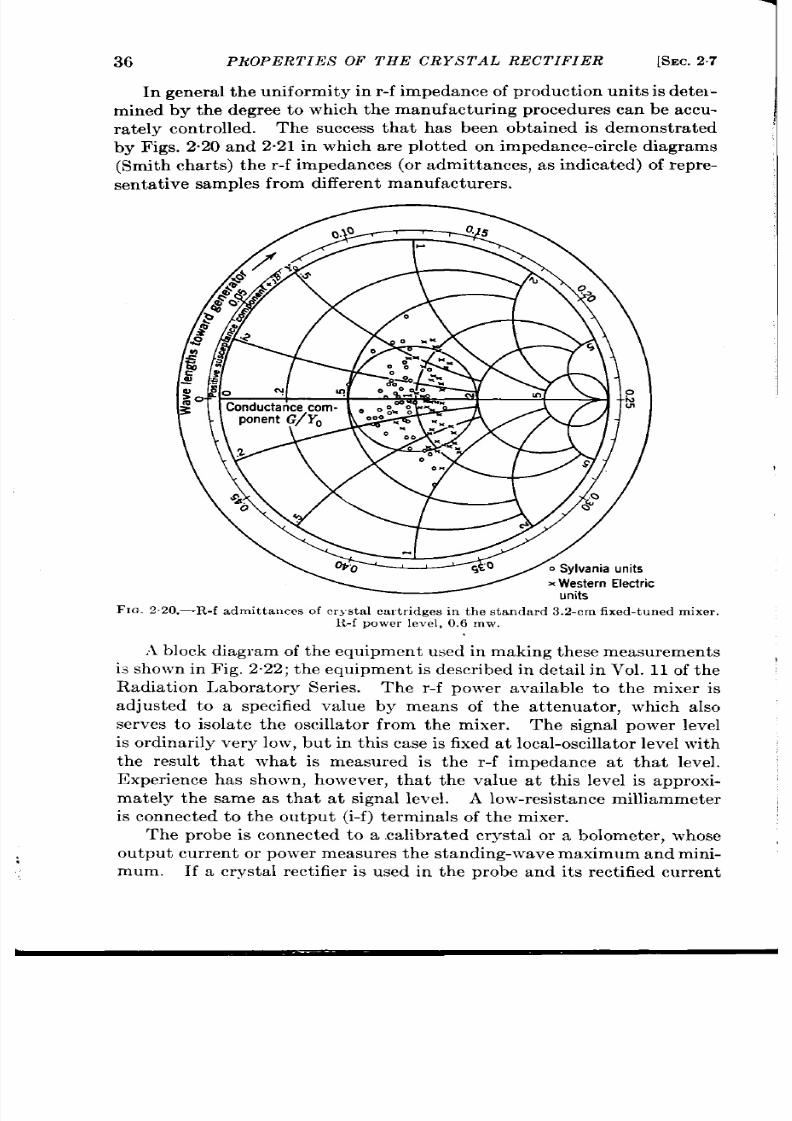
36
PEOPERTZES OF THE CRYS TAL RECTIFIER [SEC.2.7
In gener al t he un iformit y in r -f im peda nce of pr odu ct ion u nit s is det e~-
mined by the degree to which the manufactur ing proce ures can be accu-
ra tely cont rolled. The success tha t has been obta ined is demonst ra ted
by F igs. 2“20 and 2“21 in which ar e plot ted on im peda nce circle diagrams
(Smith cha rt s t he r -f im pedances (or admit t ances, as in dica t ed) of r epr e-
sen t at ive samples fr om differ en t manu fa ct u rer s.
FIG. 2 .20 .—R.f admit tances of crys ta l car t r idges in the s tandard 3.2-cm fixed-tuned mixer .
R-f powe r level, 0.6 mw.
.1 block diagr am of t he equipment used in m akin g t hese m easur em ent s
is shown in Fig. 2.22; the equipment is descr ibed in deta il in Vol. 11 of the
Ra dia tion La bor at or y Ser ies.
The r -f power available to the mixer is
adjusted to a specified value by means of the a t t enuator , which also
serves t o isola te the oscilla tor from the mixer .
The signal power level
is or din ar ily ver y low, bu t in t his ca se is fixed a t loca l-oscilla tor level wit h
the result tha t what is measured is the r -f impedance at tha t level.
Exper ience has shown, however , tha t t he value at th is level is approxi-
mate y the same as that a t signal level.
A low-r es is tance milliammeter
is co nected to the ou tpu t (i-f) terminals of the mixer .
The probe is connected to a ca libra ted crysta l or a bolometer , whose
outpu t cur ren t or power measures the standing-wave maximum and mini-
mum. If a crysta l rect ifier is used in the pro~e and its rect ified cur ren t
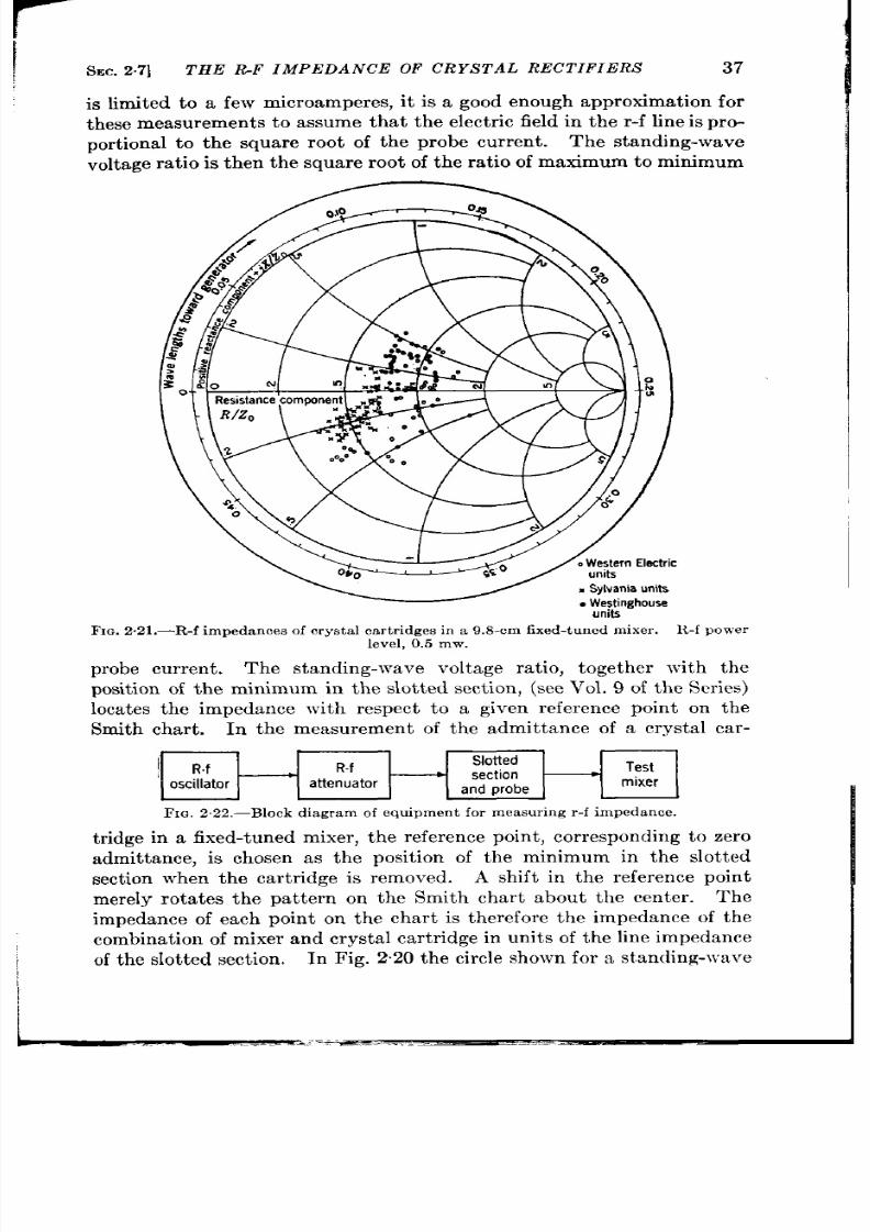
is limited
THE R-F IMPEDANCE OF CRYS TAL RECTIFIERS
37
t o a few microampere, it isagood enough approximat ion for
th ese measur em ent s t o assume that t heelect ric field in t he r -f lineispr o-
por t ional to the square root of the probe cur rent . The standing-wave
volt age ra t io is then the square r oot of the ra t io of maximum to minimum
~ Z ; ;
units
F1&2.21.-R-f impedances of cr ys ta l ca r t ridges in a9.8-cm fixed -t u ,md mixer . I t-f power
level, 0.5mw.
probe current . The standing-wave volt age ra t io, together with the
posit ion of theminimum inthe slot ted s t ion , (see Vol. 9ofthe Ser i s)
loca tes the impedance with respect to a given reference point on the
Smith char t . In the measurement of the admit tance of a crysta l ca r-
1
R.f
—
R.f
Slotted
—
section
—
Test
oscillator
attenuator
and probe
mixer
FIG. 2 .22.—Block d iagram of equ ipmen t for measu r ing r -f impedance.
t r idgein a fixed-tuned mixer , the eference point , cor responding t o zero
admit tance, is chosen as the posit ion of the minimum in the slot ted
sect ion when the car t r idge is removed.
A shift in the refer ence poin t
merely rota tes the pat t ern on the Smith char t about the cen er .
Th e
impedance of each point on the char t is therefore the impedance of the
combinat ion of mixer and crysta l ca rt ridge in units of t he line impedan ce
of the slot t ed ~ect ion . In Fig. 220 the circle shown for a st anding-wa~’e

3& PROPEiiT IES OF THE CRYSTAL RECTIFIER
[SEC. 27
volt age r at io of 2.0 includes all units for which t he r eflect ion loss is equal
to or less than 0.5 db. A waveguide mixer is t he st an da rd typeu sed in
the 3-cm region; the crysta l is shunted across the guide, and in this case
it is consequent ly conven ient o plot admit tances.
In the 3-cm band
it can seen from the char t tha t the spread in susceptance is larger than
the spread in conductance. In system-mixer design in the 3-cm band the
crysta l has been so placed in rela t ion to the TR switch that the TR
Resistance
omponent
I ?I u . 2.23.—Change of r -f impedance wit h r cct n led crys ta l cu r r en t . Tho number s indica t e
rect ified cu r ren t in millmmperes , X,.f = 9 ,8 cm.
s\ vitch can tune out the susceptance of the crysta l; in th is case, t he mis-
match found is caused by conductance a lone.
Figure 2.21 shows the impedance dist r ibu t ion in the standard coaxia l
fixed- uned test mixer at a wavelen@h of 9.% cm. The standard tun ing
of th is mixer has since been changed to the cen ter of th is dist r ibut ion .
There is no cor rela t ion between the impedance dist r ibu t ions at 10 and
3 cm. This ar ises in par t fr om the physica l differ ences in the coaxia l and
wavegu ide m xer s and in par t from the difference in fr equencies; at the
higher fr equency the physica l dimensions of the element s of the car t r idge,
wh ich determine the impedance, are a sizable fr act ion of a wavelength ,
and the car t r idge is a shunt element in a m-avegu ide ra ther than a ser ies
elemen t in a coaxia l line.
t

SEC.2.7]
THE RF IMPEDANCE OF CRYSTAL RECTIFIERS
39
The effect on r -f impedance of varying the r -f power level is shown in
Fig. 2.23. The numbers a t each point on the char t give the rect ified
crysta l cur ren t in milliamperes for which that par t icula r impedance was
obta ined. The var ia t ion of crysta l cu r r en t over the range from 0.25
to 1.0 ma, t he r egion where mixers a re ordinar ily opera ted, does not
r esu lt in a sign ifica nt ch an ge in r -f im peda nce.
F IG.2.24.—R-[ admit t ance a s a funct ion of fr equency. The poin t s a r e number ed
of increasing wavelength.
in order
The var ia t ion of impedance with frequency for the coaxia l-type car -
t r idge (1N26 type), designed for use at 1.25 cm, is shown in Fig. 2.24.
It must be remembered that the frequency sensit ivity is a funct ion of t he
cr yst al ca rt ridge a nd m ixer combin ed.
Th ese m easur em ent s wer e m ade
using a crysta l holder shown in cross se t ion in Fig. 2.25. The wave-
gu ide-to-coax al t r ansformer shown is designed to provide a matched
terminat ion to standard +- by +in . wavegu ide when the coaxia l crysta l
r ecept acle is termina ted in a 65-ohm line.
A t ransformer of th is t ype is
employed in many of the mixers used in the l-cm radar systems.
The r -f impedances shown in Fig. 2.24 were measured over a wave-
length range from 1.213 to 1.287 cm, cen tered at 1.250 cm. The small
var ia t ion observed over th is range for the standard coaxia l t ermin at ion
indica tes tha t most of the var ia t ion in impedance is in the crysta l car t r idge
itself.

.—
40
PROPERTIES OF THE CRYSTAL RECTIFIER
[SEC.28
The r -f impedance is a complica ted funct ion of car t r idge g omet ry,
size and shape of car t r idge par ts, composit ion of the semiconductor , and
whisker pressure. It is very difficult therefore, in the case of the ceramic
car tr idge, t o adjust t he r -f impedan ce wit hou t affect ing ot her pr oper ties
of the r t if er . In th is respect a car t r idge of the coaxia l type has the
advan tage of sufficien t space in the pin end for the inser t ion of a coaxia l
kf and d+ terminals
/
I rsu’a’’ngkd
II
R.fchoke
/
t r an sformer wh ich , wit hin lim it s, will
match a given crysta l impedance to
a 65-ohm line.
2.8. The I-f Impedance of Crys-
tal Rect ifier s.-A mat ter of pr ime
im por tance in t he design of coupling
II /
circuit s bet ween t he m ixer and t he i-f
LI
Insulating bead
FXG.2 .25.—Cross sect ion of crysta l holder
for t h e 1N26 ca r tr idge.
amplifier is the i-f impedance that is
seen on lookin g n to t he i-f t ermin als
of a cr yst al m ixer . Th e i-f im peda nce
per t inen t her e is tha t a t the outpu t
t erminals of the mixer when the r ec-
t ifier is dr iven by a local oscilla tor .
The value of the i-f impedance is
found to depend n the condit ions
under which it is measured. It is a
funct ion of t h e loca l-oscilla t or power
level and depends on the r -f proper -
t ies of the mixer and the circuit con-
nected to the r -f input terminals of
the mixer . Finally, for a given mix-
er and measur ing equipment , he i-f
im peda nce of commer cia l r ect ifier s,
like ot her cryst al quant it ies, shows a
spr ead of valu es occu rr in g even wit h
ca refu lly con tr olled manufa ct ur in g
techniques. In th is chapter nly
typica l data on s me of these effect s will be presen ted. The theoret ica l
t r ea tment will be found in Chap. 5.
Measurem en t of I-j Im pedance and D-c Res is t ance.—The i-f impedance
an be measured with an impedance br idge designed to opera te a t the
des ired in termedia te frequency.
At t he Radia t ion Labor at or y a Sch er in g
br idge designed by eers* to opera te a t 30 Me see has been found
satisfactory.
The dynamic low-frequency (d-c) resist ance is of in terest since the
theory of frequency conversion predict s tha t for crysta l mixers used
I Y. Beers,
“A 30-Mc Sch er in g Br idge,” RL Repor t No. 61-19, ~I ay 12, 1943.
r
SEC.2.8]
THE I-F IMPEDANCE OF CRYSTALS
b
41
with 1ow-Q r-f systems, as is the case in crysta l t est equipment , the i-f
and d-c conductance are the same.
The d-c resist ance can be easily determined on the assumpt ion that a
crysta l excit ed by a local oscilla tor is equivalent to a d-c gener ator with
an internal resist ance. This d-c resistance is determined by measur ing
(1) the shor t -circuit cu r ren t , and (2) the cur ren t in to a given external
load. The d-c resist ance R is obviou sly given by t he expr ession
R= r&,
(34)
where r is the external load and k is the ra t io of shor t -circu it cu r rent to
the ur ren t when the load r is used.
The assumpt ion of equ ivalence to a
genera tor llows this method to be used with good result s when k is n ot
grea ter than 2.
The d-c resist ance may also be measured by means of a br idge oper -
a ted at low frequency, for instance, 60 cycles.
Another method is to
apply a low-frequency source of a few volt s in ser ies with a resistance of,
for example, 100,000 ohms to the i-f terminals. Since the d-c resistance
. .
of th e mixer is a few h un dr ed ohms, this ar ran gem ent pr ovides essent ia lly
a constan t -cur ren t sour ce. The d-c resistance can then be determined
by reading the volt age across the i-f terminals with a suitable voltmeter .
A com ar ison of t he i-f and d-c r esista nces m easur ed at t he Radia t ion
La bor at or y by Hun tin gt on u sin g t he for egoin g met hods sh ows good a gr ee-
ment for the standard 10-cm test mixer .
A similar result has been
r epor t ed by Smith2 in which the i-f resistance is measured with the aid of
a d ode noise source. Other in est iga tor s, however have found a dis-
crepancy between the i- and d-c re~lstances, the former running 10 to
35 per cen t lower than the la t ter .
A discrepancy of about 25 per cent is
found, for example, in the mixer used in the 3-cm standard test equip-
ment . Smith3 has offered the suggest ion that the discrepancy is mainly
a funct ion of the r -f appara tus us d in the measurement .
According
t o hk t heor y, t he i-f volt age applied t o t he i-f t er minals for t he impedan ce
measurement modula tes the r -f wave reflected by the crysta l. Par t of
the modula ted wave is then reflected back ag in to the crysta l by tuning
mechanisms or other discont inuit ies in the r -f line. Par t of th is is
absorbed by the crysta l, the remainder being again re lected, and so on.
As a result of th is process, componen ts from the r eflected modula ted
wave ar r ive at the crysta l in var ious phases with respect t o the applied
I H. B. Hunt in gt on , u n publish ed da ta .
z R. N. Smith ,
“ Crysta l Noise as a Funct ion of D-c Bias and 30-Mc Impedance
Mea su r ed wit h a Diod e Noise %u r cc,
“ OSRD Con tr act , OIt Msr -362, Sec. D-1, NDRC
Repor t, P ur du e U niv., J u ne 25, 1943.
s R. N. Smith ,
Mixer
Con st an ts,” OSRD Con tr act , OEMsr -362, Sec. D-1, NRDC Office, Ma r. 24, 1944.
1
(
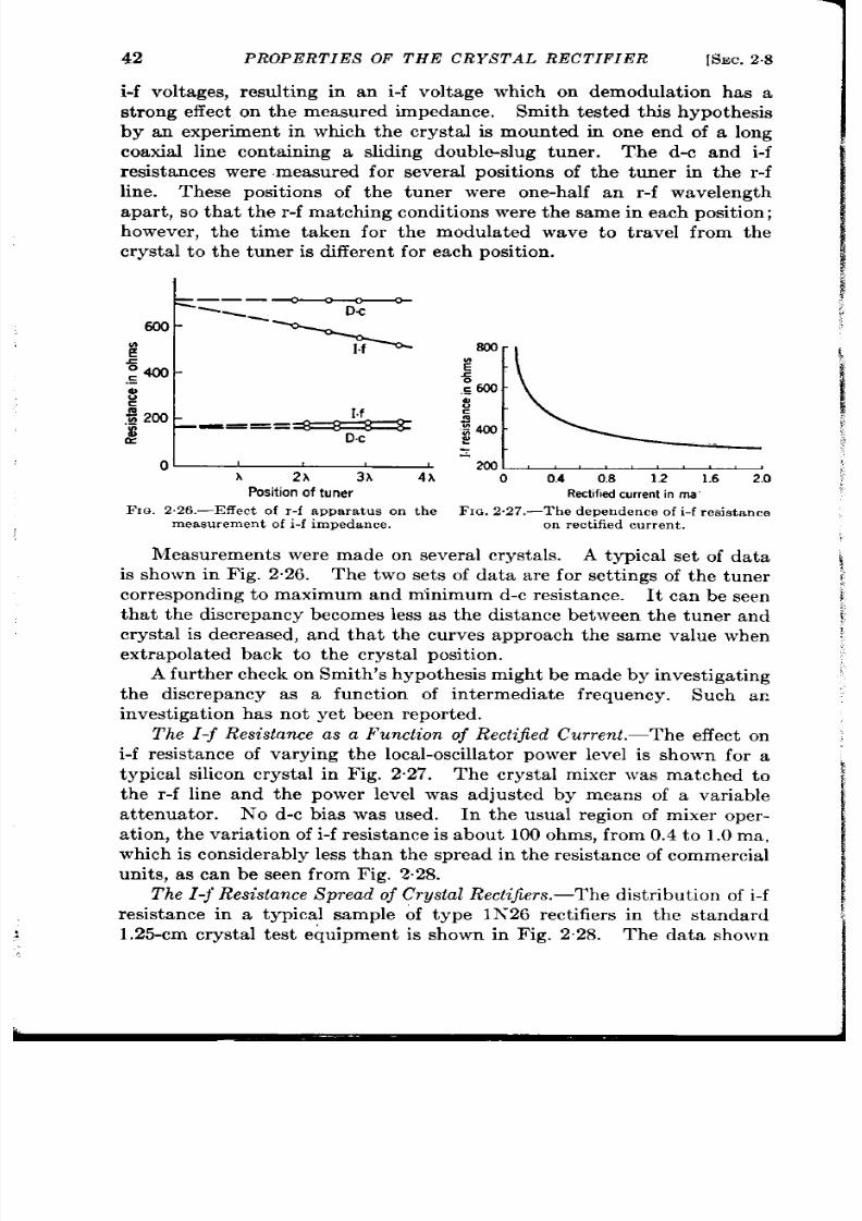
42
i-f volt ages ,
s t rong effect
PROPERTIES OF THE CRYSTAL RECTIFZ17R
[SEC. 28
result ing in an i-f voltage which on demodula t ion has a
on the measured impedance. Smith test ed this hypot esis
by m- exper iment in which the c~ysta l is oun ted in one end o; a long
oaxia l line conta in ing a sliding double-slug tuner .
The d-c and i-f
resistances were measured for severa l posit ions of the tuner in the r -f
line. These posit ions of the tuner were one-half an r -f wavelength
par t , so t hat t he r -f matching condit ions wer e th e same in each posit ion;
however , the t ime taken for - the
crystal to the tuner is different for
modula ted wave
each posit ion .
to t ravel ~rom the
p“-===:==+:==
j+, ,,,
A
2A
3A 4A
o 0,4 0.s
1.2 1,6 2.0
Positionof tuner ect!ledcurrentin ma’
F IG. 226.-E ffect of r -f a ppa ra tu s on t he F IG. 2.27.—Th e depen den ce of i-f r esist an ce
measurement of i-f impedance .
on rect ified current .
Measurements were made on severa l crysta ls. A typical set of data
is shown in Fig. 2.26. The two set s of data are for set ings of the tuner
cor respon din g t o ma ximum an d minimum d-c r esist an ce.
It can be seen
that the discrepancy becomes less as the distance between the tuner and
crystal is decreased, and that the curves approach the same value when
ext rapola ted back to the cryst l posit ion .
A fu rt her ch eck on Smit h’s h ypot hesis m igh t be m ade by in vest iga tin g
the discrepancy as a funct ion of in termedia te frequency. Such ac
invest igat ion has n ot yet been r epor ted.
The I-f Resistance as a Function of Recti~ed Cu rr en t.—The effect on
i-f resistance of varying the local-oscillator power level is shown for a
typica l silicon cr ysta l in Fig. 2.27.
The cr sta l mixer was matched to
the r -f line and the power level was adjusted by means of a var iable
a t tenuator . No d-c bias was used.
In the usual region of mixer oper -
a t ion, t he var iat ion of i-f r esistance is abou 100 ohms, from 0.4 t o 1.0 ma,
wh ich is con sider ably less t han t he spr ea d in t he r esist an ce of commer cia l
unit s, as can be seen from Fig. 2.28.
T he I-f Resistan ce S pread of Crystal R ectifiers.-T he dist r ibu tion of i-f
r esistance in a typica l sample of type 1N26 rect ifier s in the standard
1.25-cm crysta l t est equipment is shown in Fig. 2.28. The data shown
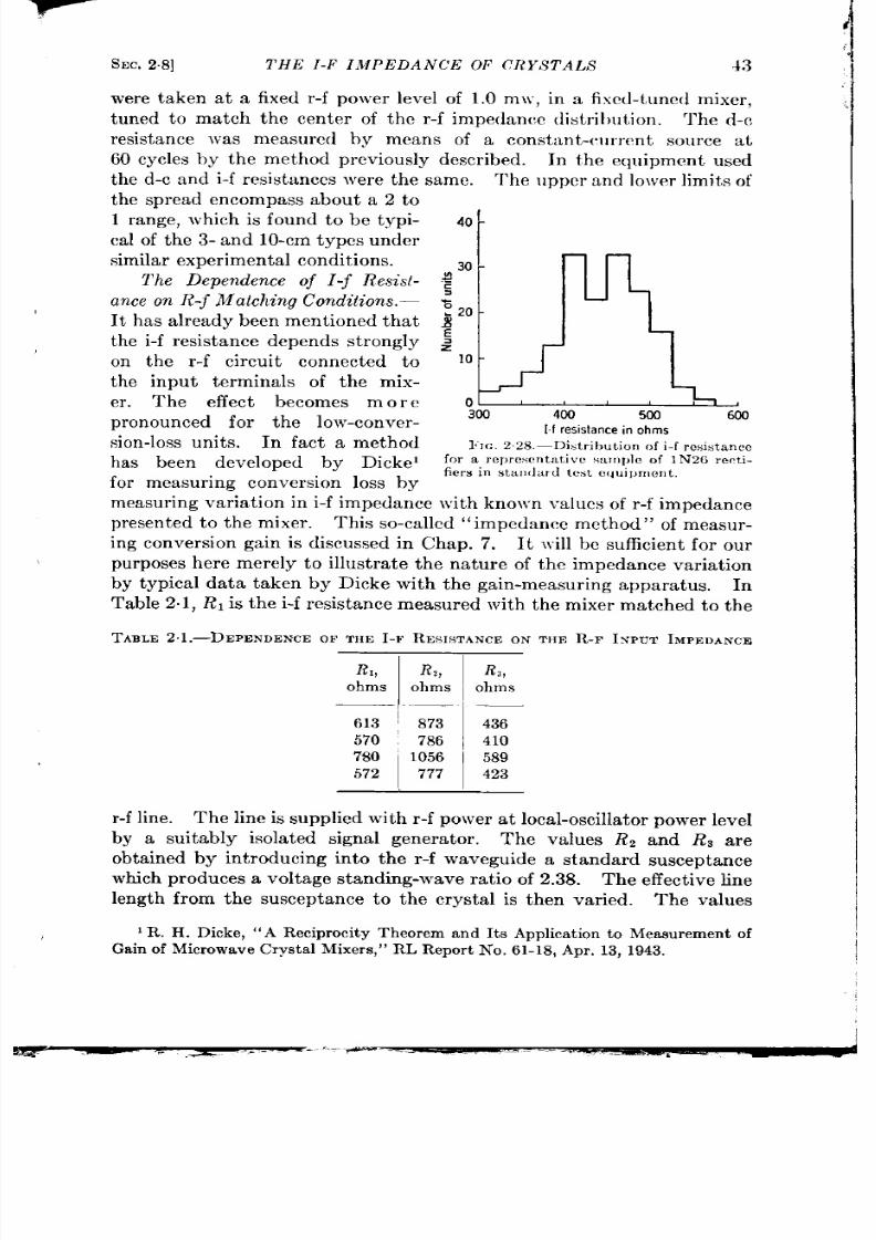
-
SEC,2.8] THE I-F IMPEDAN CE
were taken at a fixed r -f po~ver level of
OF CRYSTAL S
43
1.0 m}v, in a fixed-tu ned mixer ,
t uned to match the cen ter of the r -f impedance dist r ibu t ion . The d-c
resistance was measured h .y means of a constan t -c llr rcn t sou rce a t
60 cycles y the method previously descr ibed. In the equipment used
the d-c and i-f resistances were the same.
‘f’h e u pper a nd lower limit s of
the spread encompass about a 2 to
1 range, wh ich is found to be typi-
ca l of the 3- and 10-cm types under
s imila r exper imen ta l cond it ions.
The Dependence of Z -f Res st-
ance o R -f Match in g Conditions.—
It has a lready been ment ioned tha t
t he i-f r esist an ce depen ds st ron gly
on the r -f circu it connected to
the input termina ls of the mix-
er . The effect becomes m o r e
pronounced for the low-conver -
sion-loss units. In fact a method
has been developed by Dicke’
for measur ing conver sion loss by
40
t
30
-
r
-
S
%
. 2 0
+
2
10
-
0
300
400
500 600
If resstance in ohms
l:l(;. 2 2S.—Distrit>uti0n of i-f resistan ce
for a r cpr cs cn t at ivc w!r )l)le of 1N26 r ect i-
fie rs in s ta t ,dard t cbt equ ipmen t .
mea su rin g va~la tion in i-f impedance ~vit h knowm \ -a lu cs of r -f impedan ce
presen ted to the mixer . This so-ca lled “ impedance method” of measur-
ing conversion gain is discussed in Chap. 7. It will be sufficien t for ou r
purposes h er e mer ely t o illustra te t he na ture of t he imp dance var ia t ion
by typica l da ta taken by Dicke with the gain-measuring appara tus. In
Table 2.1,
RI is
t he i-f resistance measured with the mixer matched to the
TAELE 2.1.—DEPENDENCEOF THEI -F RESISTANCEON THE R-F INPUT IMPEDANCE
R,, R ,,
R ,,
ohms
ohms ohms
613 873 436
570
786
410
780
~
1056
589
572
777
423
r -f line. The line is supplied with r -f power a t loca l-oscilla tor power level
by a suitably isola ted signa l genera tor . The values Rz and R8 are
obta ined by in t roducing in to the r - waveguide a standard susceptance
which pr odu ces a volt age standing-wave ra t io of 2.38. The effect ive line
length from the susceptance to the crysta l is then var ied. The value
1R. H. Dicke, “A Reciprocity Theorem and Its Applica t ion to Measurement of
Ga in of Micr owave Cr yst al Mixer s, ”
RL Repor t N o. 61-18, Apr . 13, 1943.
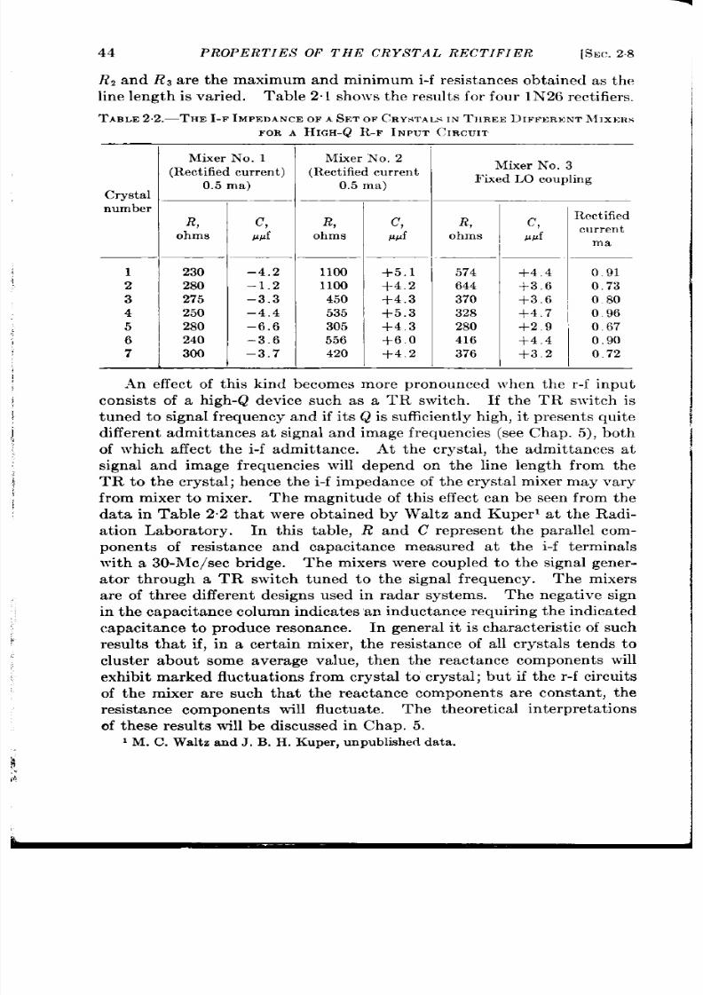
44
PROPERTIES OF THE CRYSTAL RECTIFIER
[SEC
28
R, and R S a re the aximum and minimum i-f resistances obta ined as the
lin e len gt h is va ried.
Ta ble 2.1 sh o]vs t he r esu lt s for fou r 1N 6 r ect ifier s.
TABLE2,2.—THE I-F IMPEDANCEOFASETOF
CRYSTALS INT]iREE DIEWWRENTYfIXENS
FOR A H IGH -Q R-F INPUT CIRCUIT
crystal
number
1
2
3
4
5
6
7
Mixer No. 1 Mixer No, 2
(Rect ified cu rr en t) (Rect ified cu rr en t
0.5 ma) 0.5 ma)
R,
ohms
230
280
275
250
280
240
3(KI
c,
R,
p,u f ohms
–4.2 1100
–1.2 1100
–3.3
450
–4.4
535
–6.6 305
–3.6 556
–3.7
420
c,
ppf
+5.1
+4.2
+4.3
+5.3
+43
+6.0
+4.2
Mixer No. 3
F ixed LO couplin g
R,
ohms
574
644
370
328
280
416
376
+4.4
+3.6
+3.6
+4.7
+2.9
+4.4
+3.2
Rectified
current
ma
0.91
0.73
0 80
0 96
0.67
0.90
0.72
.An effect of th is kind becomes more monounced when the r -f invut
consi t s of a high-Q device such as a TR switch . If the TR switch i
t un ed t o signal fr equ en cy and if it s Q is sufficien tly high, it pr esen ts quite
differ en t admit t ances a t signal and image fr equ encies (see Chap. 5 , bot h
of which affect the i-f admit t ance.
At the crysta l, the admit tances at
signal a d image frequencies will depen on the line length from the
TR to the crysta l; hence the i-f impedance of the crysta l mixer may vary
from mixer to mixer . The magnitude of th is effect can be seen from the
data in Table 2.2 that were obta ined by Waltz and Kuper ’ a t the Radi-
a t ion Labora tory. In this table, R and C represen t ~he para llel com-
ponen t s of resist an e and capacit ance measured at the i-f terminals
with a 30-Mc/sec br idge. The mixers were coupled to the signal gener -
a re of th ree different designs used in radar systems.
Th e n ega tive sign
in t he ca pa cit an ce column in dica tes an in du ct an ce r equ ir in g t he in dica ted
ca pa cit an ce t o pr odu ce r eson an ce.
In gener al it is char act er ist ic of su ch
result s tha t if, in a cer ta in mixer , the resistance of all crysta ls tends to
cluster about some average value, then the reactance component s will
exhibit marked fluctuat ions from crysta l to crysta l; but if the r -f circuit s
of the mixer a re such that the reactance component s a re constant , the
r esist an ce compon en ts will flu ct ua te.
Th e t heor et ica l in ter pr et at ion s
of these r sults ll be discussed in Chap. 5.
I M C. Waltz and J . B. H. Kuper ,unpublished .data .

CHAPTER 3
PROPERTIES OF SEMICONDUCTORS
In this chapter some of the under lying ideas of modern solid sta te
theory are qualita t ively reviewed with part icu lar emphasis on the elec-
t ron t heor y of sem icon du ct or s.
A few quant ita t ive result s are sta ted
but not der ived. The discussion is rest r icted to those aspects of the
subject that bear on the problem of contact rect ifiers and that will be of
use in the succeeding chapters, especia lly Chap. 4. The reader who
desires a broader and more detailed account is refer red to the many
excellen t t ext s on solid-st at e t h eor y. I
3.1. Ba nd Th eor y .-Th e cla ssifica tion of cr yst allin e mat er ia ls a ccor d-
ing to their electr ica l and opt ical proper t ies and the detailed s udy of
each of the severa l classes is enormously facilita ted by the ban d th eory,
which plays a role in the physics of solids that is ana logous and of com-
parable impor tance to the concept of energy levels in the theory of
in dividu al a toms and molecu les.
Indeed there is not only an analogy but a direct connect ion between
the elect ronic en ergy levels of an individual fr ee a tom and the elect ronic
ener gy bands of a solid material consist ing of a collect ion of a toms form-
ing a crysta l la t t ice. The elect ronic energy bands of the la t t ice may be
considered to be der ived from the atomic en ergy levels of the free a toms.
In some cases there is a one-to-one correspondence between the lat t ice
bands and the atomic levels from which they are der ived; in other cases
t he connect ion is less dist in ct .
This connect ion may usually be t r ced by imagin ing the lat t ice to
be formed by bringing together a collect ion of atoms from a state of
remote separa t ion to the final sta te, namely, the equilibr ium separa t ion
found in the actual crysta l lat t ice. The reader is r efer red to the standard
works cited for a descr ipt ion of the manner in which this connect ion
between the a tomic levels and the lat t ice bands can b established. It
will suffice h ere t o sta te that , in the lat t ce, th ere are a number of a llowed
values of energy accessible to an electron .
hese energy sta tes are
1See F. Seitz, T he Mod ern T heory of Solids, McGr aw-Hill, New York, 1940; R. H.
Fowler , Stat ist ical Mechanics, 2d cd., Cambr idge, Lon don, 1936, Chap 11; A. H.
Wilson, T he T heory of Metals, Cambr idge, Imn don , 1936; N“. F. Mot t and H J ones,
T he T heory of the Propert ies of Metals and A Uoys , Oxford, New York, 1936; A. H.
Wilson, Metals and Sem i conduct or s, Cambr idge, London , 1939; and N. F. Mott and
R. W. Gu rn ey, E lect ron ic Proc.eses in I on ic Cryst als, Oxfor d, N ew Yor k, 1940.
45
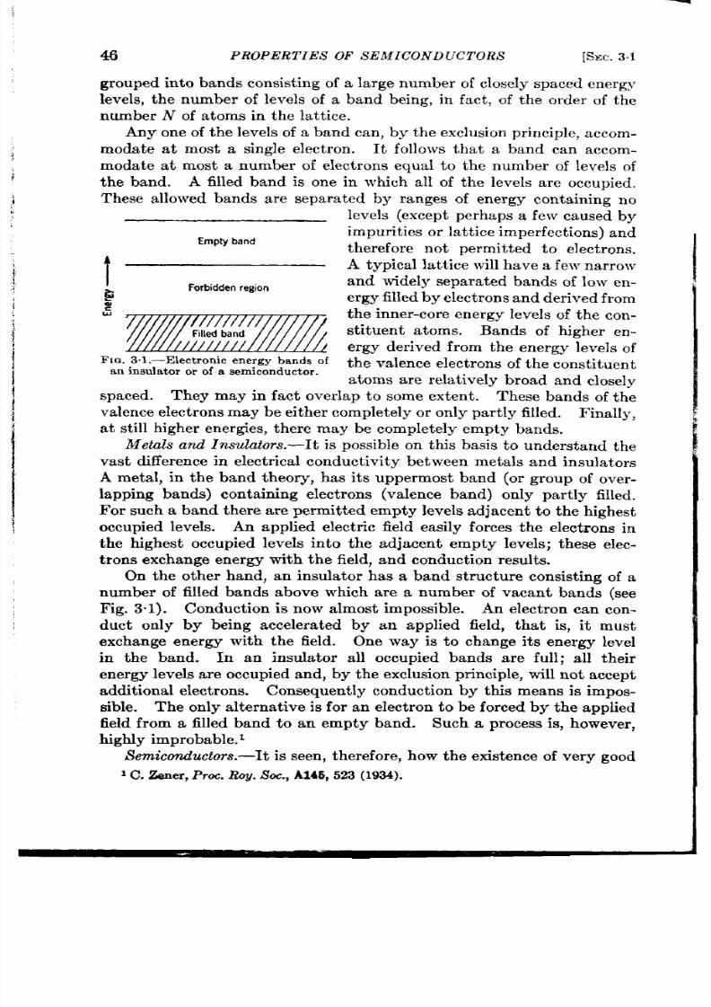
46
PROPER TIES OF S EMICONDUCTOR S
grouped in to bands consist ing of a la rge number of closely
[SEC.31
spa ced en er gv
ievels, th e number of levels of a band being, in fact , of the-order of t ie
number N of atoms in the la t t ice.
Any one of the levels of a band can , by the exclusion pr inciple,
accom-
moda te a t most a single elect ron .
It follows that a band can accom-
moda te a t most a number of elect rons equal to the number of levels of
the band. A filled band is one in which all of the levels a re occupied.
These a llowed bands a re sepa ra ted by ranges of energy con ta in ing no
Emptyband
I
~
Forbiddenegion
&
y
/////////
Filledband
/////////
L
FIG. 3.1 .—Elect ron ic ene rgy bands of
an insula tor or of a semiconductor .
levels (except perhaps a few caused by
impu rit ies or la tt ice im per fect ion s) a nd
therefore not permit ted to elect rons.
A typica l la t t ice will have a few n arrow
and widely sepa ra ted bands of low en-
er gy filled by elect ron s a nd der ived fr om
the inner -core en ergy levels of the con-
st ituent a toms. Bands of h igher en-
ergy der ived from the energy levels of
t he va len ce elect ron s of t he con st it uen t
a toms are rela t ively broad and closely
spaced. They may in fact over lap to some exten t . These bands of t ie
va len ce elect r on s may be ith er com pletely or on ly pa rt ly filled. Fina lly,
a t st ill h igher energies, th ere may be completely mpty bands.
Metals and Insulators.—1t is possible on th is basis to understand the
va st iffer en ce in elect r i a l con du ct ivit y bet ween m eta ls and insula tors
A meta l, in the band heory, has it s upper ost band (or group of over -
lapping bands) con ta in ing elect rons (va lence band) onIy par t ly filled.
For such a band there a re permit ted empty levels adjacen t to the highest
occupied levels. An applied elect r ic field easily forces the elect rons in
the h ighest occupied levels in to the adjacent empty levels; these elec-
t rons exchange en ergy with the field, and conduct ion resu lt s.
On the other hand, an insu la tor has a band st ructu re consist ing of a
number of filled bands above which a re a number of vacant bands (see
Fig. 3.1). Conduct ion is now almost impossible. An elect ron can con-
duct only by being accelera ted by an applied field, tha t is, it must
exchange energy with the field. One way is to change its energy level
in the band. In an insu la tor a ll occupied bands a re fu ll; a ll their
en er gy levels a re occu pied an d, by th e exclu sion pr inciple, will n ot a ccept
addit iona l elect rons. Consequen t ly conduct ion by this means is impos-
sible. The on ly alterna t ive is for an elect ron to be forced by the applied
field from a filled band to an empty band. Such a process is, however ,
h ighly improbable .1
Sem icon du ct or s. -It is seen , t her efor e, h ow t he exist en ce of ver y good
1C. Zener ,Pm t. R ov. S ot., A145,523 (1934).

SEC.
3.1]
BAND THEORY
47
con du ct or s (meta ls) an d ver y poor con du ct or s (in su la tor s) is a ccou nt ed
for by the band theory.
It remains to show how semiconductors, tha t
is, ma terials wit h in termedia te con du ct ivit ies, ca n be fit ted n to t he band
theory.
There are two dist inct types of semiconduction , int r insic and
ext r insic; they may both , however , occur in the same semiconductor .
In tr insic semiconduct ion occurs in materials that have a band st ruc-
ture similar to that of insulators (see Fig. 3“1) but with the difference
that the gap in energ between the highest filled band and the lowest
empt y ba nd is r ela tively sma ll.
At absolu te zero th e mater ia l s an insul-
a tor , but at fin ite tempera tures enough elect rons are thermally excited
from the filled to the empty band to produce a limited amount of conduc-
t ion . This conductkm is produced not only by the excited elect rons but
L
also by the elect rons of the nearly filled band. Silicon and germanium
bot h exh ibit in tr insic con du ct ion a t su fficien tly eleva ted temper at ur es.
In tr in sic con du ct i n is, h owever , of lit tle impor ta nce in cr yst al r ect ifier s.
Ext r insic semiconductors also have the band st ructure of Fig. 3.1.
E xt rin sic semicon du ction occu rs beca use of th e pr esen ce of ext ra en er gy
levels as a resu lt of lat tice im per fect ion s or of t he pr esen ce of impu rit ies.
These ext ra energy levels lie in the normally forbidden region between a
filled and an empty band and may act either as donators or as acceptors.
An extra level acts as a donator if it is filled at absolu te zero. At fin ite
f
tempera tures a donator level may donate its elect ron to the empty band.
Once i the empty band an elect ron is, of course, in a condit ion to con-
duct . An ext ra level acts as an acceptor if it is empty at absolu te zero.
At finite tempera tures an acceptor level may accept an elect ron from the
filled band and thus leave an empty level in the band. Conduct ion in
the previously filled band is now possible because an elect ron may be
t ransfer red by field excita t ion into the vacant level. In silicon and
germanium as used in rect ifiers, conduct ivity is extr insic because of the
presence of impurit ies. In silicon as used in rect ifiers the impurity
levels usually act as acceptors; in germanium, they usuall act as dona-
,
tors. In copper oxide (an ext r insic semiconductor ) the ext ra levels act
as acceptors and ar ise from lat t ice imperfect ions caused by a stoichio-
metr ic deficiency of copp r in the lat t ice.
A filled donator level is
elect r ica lly neutral and an empty dona tor level has a single posit ive
charge. On the other hand, a filled acceptor level (tha t is, one tha t has
accepted an elect ron) has a single negat ive charge, whereas an empty
a ccept or level is elect rica lly n eu tr al.
The reasons for these sta tements
are given in Sec. 3.6.
The width of the forbidden region (see Fig. 3.1) is severa l elect ron
germanium. It has been found that , a t least in the case of silicon and
germanium, the ext ra energy levels produced by imp r it ies lie very clese

48
PROPER TIES OF S EMICONDUCTOR S
[SEC.32
(tha t iswithin O.l ev) totheband towhich they donate or from which
they accept elect rons. Thus donator levels lie below and very close to
the’’ empty” band, andacceptor levels lie above and very close to the
“filled” band. A possible reason for th is fact has been suggested by
Betheand isgivenin Sec. 3.6.
3.2. Elect ron Dist r ibut ion in Semiconductor s.-It will be shown in
Chap. 4 that a knowledgeof t heelect ron dist r ibut ion in semiconductor s
is vita l to the underst anding of the rect ifica t ion process.
It was shown
in the previous sect ion that conduct ion is the resu lt either of a few elec-
t rons in a normally “empty”
band, or of a few vacancies in a normally
‘‘ filled” band, or in som e cases of a combinat ion of t he t wo.
It can be shown that in the first case, tha t is, tbe case of a few elec-
t rons in the normally empty band, these elect rons act as a fr ee classical
assembly. Their velocity is zero at the bot tom of the band and increases
propor t ionally t o the square root of their energy measured from the bot -
tom of the band. Their effect ive mass, however , may be la rger than the
normal mass of a fr ee elect ro . Since they are few in number , they do
not form a degenera te gas as do the ‘(free” elect rons in meta ls but obey
t h e cla ssica l Maxwell-Bolt zmann st at ist ics.
The elect rons of a near ly filled band, however , behave in a very dif-
feren t manner . Since almost all of the available energy levels are filled,
t he elect ron gas is h igh ly degen er at e.
The velocity of n elect ron is zer o
at the top of the band and increases with decreasing energy in the band.
This anomaly is rela ted to the fact tha t the effect ive mass of an elect ron
near the top of the “filled” band is negat ive. In fact , the applica t ion of
an elect r ic field tha t would normally accelera te a free elect ron actually
reta rds an elect ron near the top of the “filled” band. These elect rons
thus respond to the field as though they have a posit ive r a ther than a
negat ive charge. It has been found conven ient to focus at ten t ion not
on the la rge number of elect rons of the near ly full band but ra ther on the
vacan t levels or “holes” as they are called. These holes, few in number ,
move about in the la t t ice as the elect rons fill them and leave new holes
behind. It is shown in works on solid-st a te theory that these holes act
pr ecisely as t hough t hey wer e posit ively cha rged elect rons with posit ive
mass. It is possible, in fact , to ignore the elect rons ent ir ely, tha t is, t o
suppose the band to be completely full and to t rea t the holes as a fr ee
cla ssica l n on degen er at e a ssembly of posit ive elect r on s obeyin g Maxwell-
Boltzmann sta t ist ics. The case of a near ly full band then becomes very
similar t o that of a near ly empty band with the difference that , in a near ly
full band, the cur ren t ca r r ier s (holes) a re posit ively charged with en er gy
(and velocit y) increasing fr om t he t op t o t he b t tom of t he band.’
1For a more complete t rea tmentof the concept of holes s ee, for example, F . S&tz,
T he Mod em T heory of S old , McGraw-Hill,New York , 1940, Sec. 68.
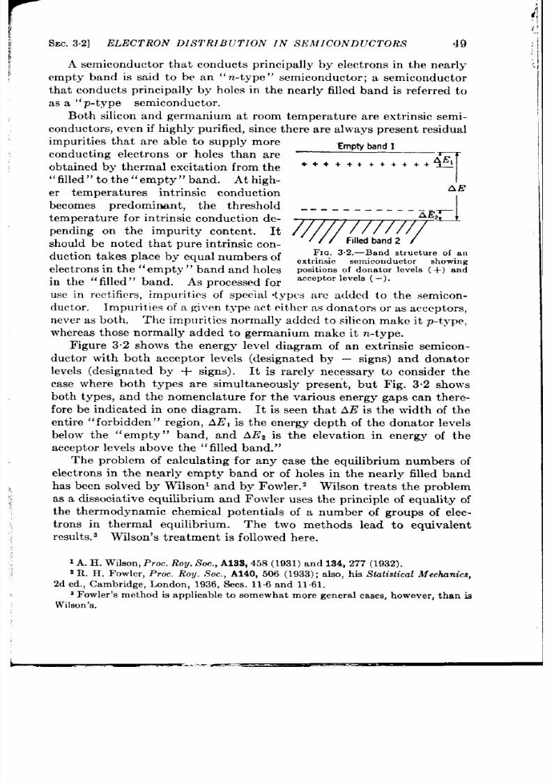
1
SEC.3.2]
ELECTRON DIS TRIBUTION IN S EMICONDUCTORS
49
A semiconductor that conduct s pr incipally by elect rons in the near ly
empty band is sa id to be an “ n-type”
semiconductor ; a s emiconductor
that conduct s pr incipally by holes in the near ly filled band is refer r ed to
as a “p-type semiconductor .
Both silicon and germanium at room temperatu re are ext r insic sem -
con du ct or s, even if h igh ly pu rified, sin ce t her e a re a lwa ys pr esen t r esidu al
impur it ies that a re able to supply more
conduct ing elect rons or holes than are
obta ined by therma excit a t ion from the
filled” to the” empty” band. At high-
er t empera tu res in t r insic conduct ion
becomes predominant , the threshold
t emper at ur e for in tr in sic con du ct ion de-
pending on the impur ity conten t . It
should be noted that tmre int r insic con-
duct ion takes place b; equal numbers of
lect rons in the “empty” band and holes
in the “filled” band. As processed for
Empty band1
++++++++++++
7
Lyg
AE
----- ----- ___
///////
J
E2-
Filled band 2
F IG. 3.2.—Band st ru ct ur e of a n
ext rin sic sem icon du ct or sh owin g
posit ion s of don at or levels (+) a nd
acceptor leve ls ( -).
use in rcct ificrs, impur it ies of specia l types arc added to the semicon-
ductor . Impur it ies of a given t ype act eit her as don at ors or as a ccept or s,
never as both . The impllr it es normally added to silicon make it p-type,
whereas those normally added to germanium make it n -type.
F igure 3.2 shows the energy level diagram of an ext r insic semicon-
ductor with both acceptor levels (designated by – signs) and donator
levels (designated by + signs).
It is rarely necessary to consider the
case where both types a re simultaneous y presen t , but Fig. 3.2 shows
both types, and the nomencla ture for the var ious energy gaps can there-
for e be indica te in one diagram. It is seen that AE is the width of the
en t ir e “forbidden” region, AE 1 is the energy depth of the dona tor levels
below the “empty” band, and AE2 is the elevat ion in energy of the
a ccept or levels above t he “filled band. ”
elect rons in the near ly empty band or of holes in the near ly filled band
has been solved by Wilson’ and by Fowler . Z Wilson t rea ts the problem
as a dissocia t ive equilibr ium and Fowler uses the pr inciple of equality of
the thermodynamic chemical potent ials of a umber of groups of elec-
t rons in thermal equilibr ium. The two methods lead to equivalent
r esults. 3 Wilson’s t rea t men t is followed h er e.
I A. H. Wilson, Proc. ROV.S ot ., A19S,458 (1931)an d 134, 277 (1932).
2R. H . Fowler ,
Proc. Roy. S ot., A140, 506 (1933); a ls o, h is Sfa t is tica t Mechanics,
2d cd., Cambr idge, Lon don , 1936, Sees. 11.6 a nd 11.61.
s F owler ’s m et hod is a pplica ble t o somewh at mor e gen er al ca ses, h owever , t ha n is
Wilson’s.

50
PROPERTIES OF S EMICONDUCTOR S
Let us oonsider fir st t he case of an n-type ext r insic
[SEC.32
semiconductor
I
with NI dona tor levels per unit volume locatecl at an energy depth AE1
below the nea r ly em~ty band. Let the number of elect rons excit ed to
. .
t he nea r ly empty band be nl per unit volume. The number of bound
elect rons in the donator leyels is then N1 — nl.
Let us consider the
equ ilibr ium of t he r ea ct ion
Free elect ron + bound hole ~ bound elect ron .
The mass act ion law gives
(1)
where
KI
is t he equilibr ium constan t of the react ion .
F rom st a tis tica l
mechanical
(2)
where ml is the effect ive2 elect ron mass, k is olt zmann ’s con st an t ,
T t he absolu te t emper atu re, and h is Planck’s consta nt .
The solu t ion of Eq. (1) is
where
(3)
(4)
Two limit in g ca ses a re of specia l in ter est :
1. Weak ioniza t ion of the dona tors (n l << NJ as a resu lt of either low
tempera tu re (1” << Al?l/k) or h igh concen t ra t ion
(N ~>> v,). We obta in fr m Eq. (3) in th is case
2. St rong ioniza t ion of dona to s (nl = N,) as a resu lt
temperature
(T>> AEJ k)
or low concent r a t ion
(Nl << v,). We find in his case from Eq (3),
-N(’ -?e%)”
of don ators
(5)
of eit her h igh
of donator s
(6)
1Fowler.Statistical
Mechanics . MI . ci t.
.
1It was noted in SeC.3.2 tha t th e effectiveelectr onmaesof a latt ice electr oncliffera
in gene ra l from the maceof a fr ee norma l elect ron .
See F . Seit z, of
Solids, McGraw-Hill , New York, 1940,Sec. 68.
I

SEC.3.3] WORK FUNCTIONS AND CONTACT
Let us consider next the case of a p-type
The react ion of in terest here is
POTENTIALS
51
extr insic semiconductor .
Free hole + bound elect ron ~ bound hole.
Denot ing by nz the number of free holes per unit volume, by NZ the
number of acceptor levels per unit volume each a t the energy AEZ above
t he near ly filled band, and put t ing
(7)
wh er e mz is t he effect ive mass of a fr ee h ole, we obt ain equ at ion s pr ecisely
similar to Eqs. (3), (5), and (6), with subscr ipt s 2 instead of 1.
Fina lly, there is the case of an int r insic semiconductor . By similar
methods we find for the number nl of fr ee elect rons per unit volume (in
the near ly empty band) which in this case is equa l to the number na of
fr ee holes per unit volume (in t he near ly filled band),
nl=n2=fi2e
‘$T,
(8)
where AE is the energy separa t ion of the two bands.
3.3. Work Funct ions and Contact Poten t isls.-As will be shown in
Chap. 4, the contact poten t ia l differ ence between a metal and a semi-
conductor is of the grea test impor tan e in the theory of rect ifica t ion . If
t wo substances are placed in conta ct it is found tha t the elect ri a l pot en-
t ia l of on e substance in genera l differs from tha t of th e oth er b an amount
ch ar act er ist ic of t h e two mat er ia ls.
Th is differ en ce in pot en tia l is ca lled
t he ‘i cont act poten t ia l difference. ”
The con tact poten t ia l differen ce
between two meta ls is a lmost equa l to the difference between their work
functions.
The work funct ion of a mater ia l is t he work required to
ext ract an elect ron from it and remove it t o infinity.
Th e con ta ct
pot en tia l differ en ce bet ween a m et al a nd a sem icon du ct or is a lso a ppr oxi-
mately equa l to the differ ence of their work funct ions, a lthough th is
approximat ion is poorer than for the case of a meta l-metal conta ct .
For
a meta l-semiconductor contact , t he discrepancy between the contact
1
,
I
1
I
:,
poten tia l differ en ce a nd t he wor k fu nct ion differ en ce is of t he or der of
lcTJ
which is about 0.025 ev at room tempera ture.
The conta ct poten t ia l
differ en ce, on t he ot her h and, is gen er ally bet ween 0.2 a nd 0.5 ev.
The work funct ion x of a semiconductor depends on the amount and
type of impurit ies present . The var ious cases can be worked out , using
F owler ’s m et hods, 1wit h t he r esu lt s:
1R. H . Fowler ,
Proc. R oy. S ot.,
A140,506 (1933) or S@&icaL
Mechanics,
2d ed .,
Cambridge,London, 1936, sec. 11$“,
/
%?/, +,
E G. & G. LIBRARY
;>.. ~-.,:
“ z/ >,”
~$ VEGAS f31UlNCH
W<>>
.,
.——
—.
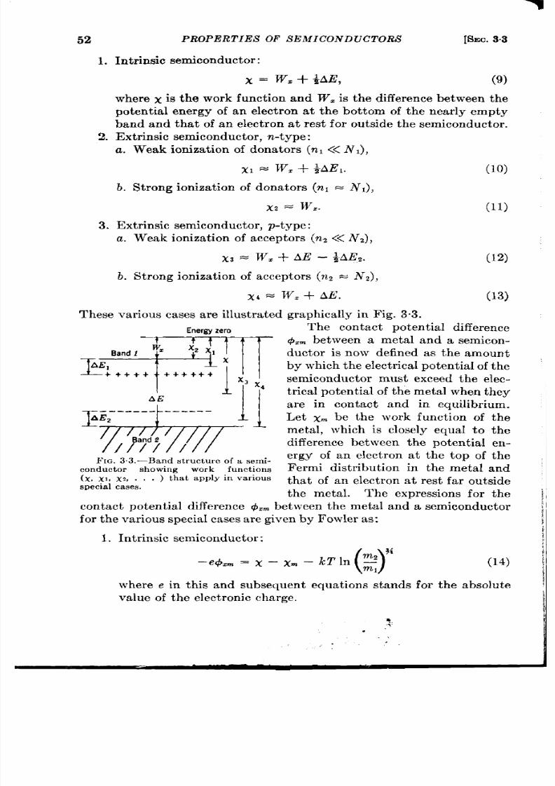
52
PROPER TIES OF S EMICONDUCTOR S [b’EC.3.3
1. Int r in sic semiconductor :
x = W. + iAE,
(9)
where x is the work funct ion and W= is the dh lerence between the
poten t ia l energy of an elect ron at the bot tom of the near ly empty
band and that of an elect ron at rest for outside the semiconductor .
2. Ext r in sic semiconductor , n-type:
a.
b.
Weak ion iza tion of don at o& (n , << NJ ,
x1
= W. + %AE,.
(lo)
St rong ion izat ion of donators (nl = N,),
x2
= w=.
(11)
3. Ext rin sic sem icondu ct or , p-t ype:
a. Weak ionizat ion of acceptors (nz << Nz),
x3
= w, + AE – 4AE,.
(12)
b. St rong ion izat ion of acceptors (n , = N,),
X4
= W. + All.
(13)
These var iou s cases ar e illust ra ted graphically in Fig. 3.3.
Energyzero
Th e contact potential difference
&m between a metal and a semicon-
.e~
ductor is now defined as the amount
by wh ich t he elect rica l pot en tia l of t he
semiconductor must exceed the elec-
t r ica l pot en tia l of t he metal wh en t hey
‘*’1
are in contact and in equilibr ium.
Let x~ be the work funct ion of the
metal, which is closely equal to the
difference between the poten ia l en-
~lG.3.3.—Bandstr uctur eof a semi-
ergy of an elect ron at the top of the
conductor
showing
~o,k fu~,ct iou~ Fermi dist r ibut ion in the metal and
(x, xl, x,, . ) that apply in var ious
that of an elect ron at rest far outside
specialcases.
the metal. The expressions for the
con tact potent ia l difference &~ between the metal and a semiconductor
for t he var iou s specia l cases ar e given by F owler as:
1. In t rin sic semiconductor :
( )
m, “
—@m=x-xm-k Tln —
m
(14)
where e in this and subsequent equat ions stands for the absolu te
va lu e of t he elect ron ic ch ar ge,
?
..
.’
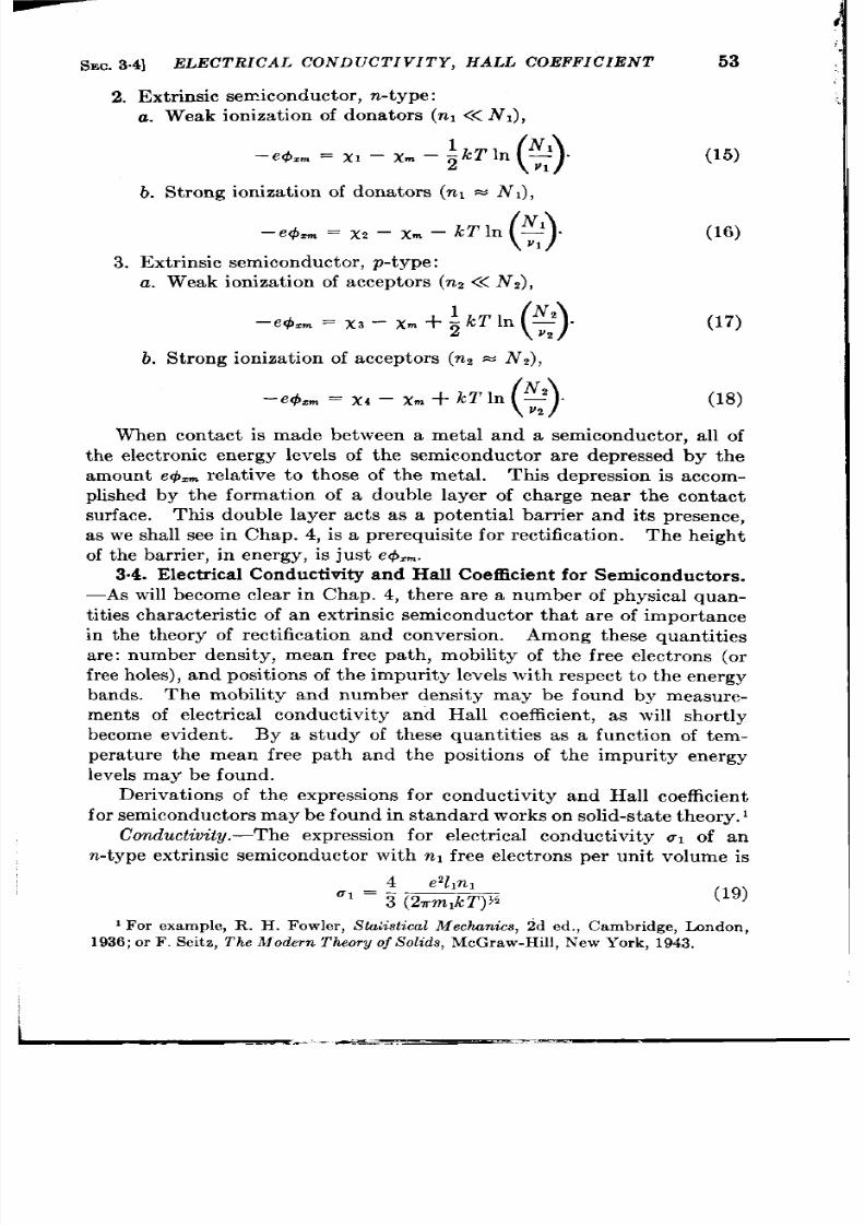
.’
.,
,,.
SEC. 3 .4]
ELECTRICAL CONDUCTIVITY , HALL COEFFICIENT
53
2. Ext rin sic sem icon du ct or , n -t ype:
a. Weak ioniza t ion of dona tor s (nl << NJ ,
( )
1
—e&. = X1 — X. —~kT ln —
VI
b. St rong ion iza t ion of donator s (nl = NJ ,
( )
,
—e4-=Xz —X. —kT ln — .
VI
3. Ext r in sic sem iconduct or , p-t ype:
a . Wea k ion iza tion of a ccept or s (7zZ<< Nz),
( )
e4=~=x3—X.+~kTln ~ .
b. St rong ioniza t ion of acceptor s (nz = N,),
( )
e4=~=xd–x. +kTln ~ .
(15)
(16)
(17)
(18)
When con tact is made between a meta l and a semiconductor , a ll of
the elect ron ic energy levels of the semiconductor a re depressed by the
amount edm rela t ive to hose of the meta l. This depression is accom-
plished by the format ion of a double layer of charg near the con tact
surface.
This double layer acts as a poten t ia l bar r ier and its pr esence,
as we shall see in C ap. 4, is a pr er equisite for r ect ifica tion .
Th e h eigh t
of the bar r ier , in energy, is just ed~.
3.4. E lect rica l Con du ct ive@ a nd Hall Coe5cien t for Sem icon du ct or s.
—As will become clear in Chap. 4, th er e a re a number of physica l quan-
t it ies ch ar act er ist ic of an ext rin sic sem icon du ctor th at a re of im por tan ce
in the theory of rect ifica t ion and conversion .
Amon g t hese qu an tit ies
a re: number density, mean free path , mobility of the fr ee elect rons (or
fr ee holes), and posit ions of t he impur it y levels with r espect t o t he en er gy
bands. The mobility and n mber density may be found by easure-
ments of elect r ica l conduct ivity and Hall coefficie t , as will shor t ly
become evident . By a study of these quan t it ies as a funct ion of tem-
pera tu re the mean fr ee path and the posit ions of the impur ity energy
levels m ay be fou nd.
Der ivat ions of the expressions for conduct ivity and Hall coefficien t
for semicon du ct or s may be oun d in standar d wor ks on solid-st ate t h or y. 1
Conduct ivity .—The expression for elect r ica l conduct ivity ul of an
n-t ype ext r insic semiconductor with n 1 fr ee elect rons per unit volume is
4
ezllnl
“ = ~ (2rm 1kT )~~
(19)
1
For example, R. H . F owler , ASt i:ist ica ZMechanics, 2d ed.,
Cambridge,London,
1936;or F. Seitz, T he Modern T heory of S olid s, McGr aw-H ill, N ew Yor k, 1943.

54
PROPERTIES OF SEM ICONDUCTORS
[SEC.
34
where 11is the mean free path of the elect rons, ml is their effect ive mass,
and the other symbols have their usual meanings.
The cor respond ing
expression for t he elect r ica l condu ct ivity of a p-t ype ext r insic semicon-
du ctor is t he same as Eq. (19) with subscr ipts 2 instead of 1 (thus refer r in g
t o th e corr espon din g quant it ies for t he fr ee holes).
The mobility of a cu rren t ca r r ier (elect ron or hole) is defined as the
mean drift velocity in unit elect r ic field. It is given by
(20)
for the case of elect ron conduct ion .
A similar expression with sub-
scr ipt s 2 in st ea d of 1 a pplies in t he ca se of h ole con du ct ion .
Compar ing Eqs. (19) a d (20) we see tha t
al =
enlbl,
(21)
and
r rz = en 2b2.
(22)
In the case of a composite semiconductor , where cu rren t is car r ied
both by elect rons and by holes, we have
u = e(nlbl +
n~bz). (23)
Hall
Efiect .-It will be seen from Eqs. (21) and (22) tha t the con-
duct ivity gives the product of the number density of cu rren t ca r r iers and
their mobility. Measurements of the Hall ffect , however , give the
number density direct ly. By combining the two measurements, there-
fore, the mobility can be determined. The Hall effect occurs when
a magnet ic field, t ransverse to the lines of cu rren t flow, is applied to a
cu r ren t -ca r ryin g conduct or or sem icondu ct or .
An emf is established in
the conductor in a direct ion or thogona l to both magnet ic field and cur-
ren t . Let us suppose tha t the cur ren t flows in the x-direct ion and tha t
the magnetic field is applied in the z-direct ion . The emf is then estab-
lished in the y-direct ion . When equilibr ium is established (with the
result tha t there is no t ransverse flow of current ), the emf is coun tered
by a n elect ric field in t he y-dir ect ion
E.,
a rising fr om ch ar ges on t he walls
of the conductor . This field E. is found to be propor t ional to the mag-
net ic induct ion
B.
and to the curren t density
J =.
The propor t ional ity
constant,
R=%.
(24)
Zz
is kn own as t he ‘f Hall coefficien t . ”
It is shown in works on solid-sta te theoryl tha t
R is
given , in the case
1For example,R . H. Fowle r, S ta~is ticaZ
Mechanics,
2d ed ., Cambr idge, I ,ond on ,
1936, 10C.cit .; or F. Seitz,TheMod ern T heory of S olidS ,
NIcGraw-Fiill,IYewYork , 1940,
10C. cit.

I
SEC. 3.4]
ELECTRICAL CON DUCTIVITY , HALL COEF ICIEN T
55
of a simple n -t ype ext rin sic semicon du ct or , by
and, in th e case of a simple p-type extr insic semiconductor , by
(25)
(26)
Since e by defin it ion is the absolu te value of th e elect ronic ch arge, we
see fr om Eqs. (25) and (26) th at t he sign of t he Hall coefficien t is n ega tive
for elect ron ic condu ct ion and posit ive for h ole c ndu ct ion .
;
The impor ance of the Hall co fficien t is due to the fact , evident from
Eqs. (25) and (26), that it gives direct ly the number densit ies of the cur-
i
r en t ca rr ier s, provided, h owe er , t ha t t he ca rr ier s a re all eit her elect ron s
or holes. For a composite semiconductor , the Hall coefficien t depends
a lso on t he n obilit ies of t he ca rr ier s.
Th e Hall coefficien t of a composit e
sem icon du ct or is given l by
(27)
wh er e b sta ds for mobility as before and subscripts 1 and 2 refer , respec-
1
t ively, t o elect ron s a nd t o h oles.
In the specia l case where nl = nz = n,
which holds for in tr insic semiconductors, Eq. (28) reduces t o
r
(28)
By combining Eqs. (25) and (21) or Eqs. (26) and (22) we see that the
elect ron ic mobilit y is given dir ect ly by t he pr odu ct of H all coefficien t a nd
conduct ivit y for a simple semiconductor ,
(29)
Variation w ith T emperatu re.—Let us now consider the tempera ture
varia t ions to be expected for u and R. The simpler case is that of R.
At high tempera tures the semiconductor is in th int r ins c range and
R
is given by Eq. (28). The sign of R eviden tly depends in th is case on th e
r ela tive magn it udes of
b I and bz . For silicon and germanium it is found
tha t
bl > b,;
tha t is, the elect ron mobility exceeds the hole mobility.
1V. A. John son , p riva t e commun ica t ion , Pu r due Un iv.
Accor din g t o Dr . J oh n son
t he ambigu it y in t he va lu e of R for a compositesemiconductor (R. H. Fowler,op. ti t .,
p . 428) has been resolvedin favor of Eq. (27).
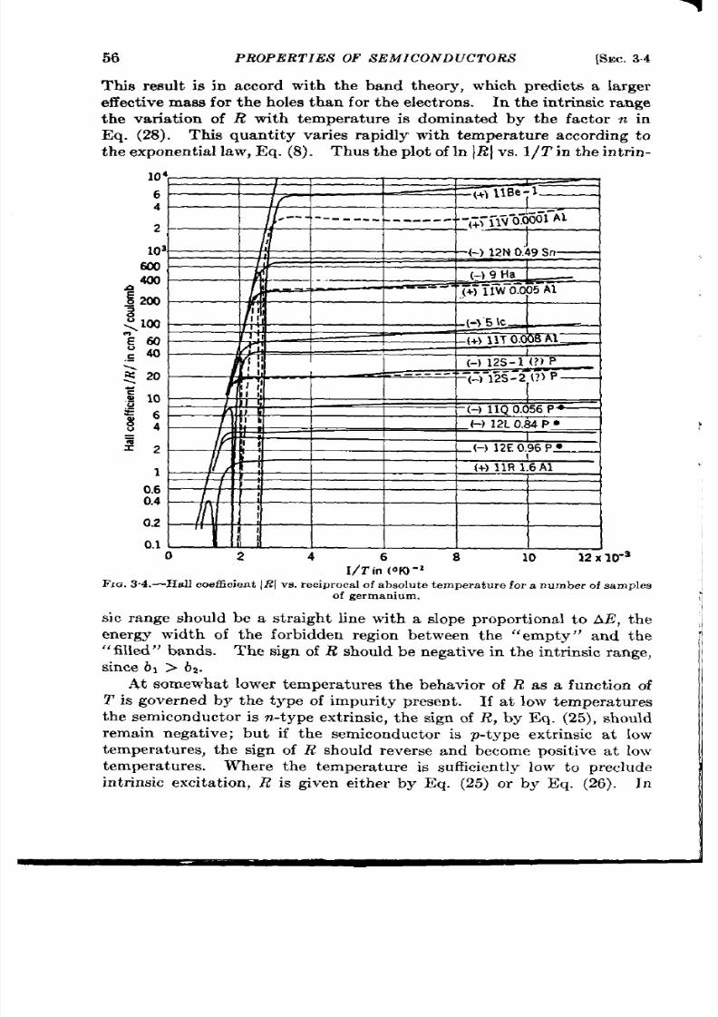
56
PROPER TI 8 OF S EM ICONDUCTOR S
[SEC.34
This result is in accord with the band theory, which predict s a la rger
effect ive mass for t he h oles t ha n for t he elect ron s.
In t he int r insic r ange
the var ia t ion of R with temperature is domina ted by the factor n in
Eq. (28). This quant ity var ies rapidly with tempera ture according to
the expo ent ia l law, Eq. (8). Thus the plot of in IR I vs. l/Tin the int r in-
II
I I
1{
,,,,,
(+)l lR 1.6A1
I
(It
1
)
/
/1) d
I
I,,!J!
I
.6
-
0.4
-
0.2
i
I
0.1
L
I
I
J
12x2
4 6
8 10
I/Tin (OK)-’
FIG.3.4.—Hall coeff ici en t IE l v s. reciprocal of absolute temperature fors number of samples
of germanium.
sic range should be a st ra ight line with a slope propor t iona l t o AE, the
energy width of the forbidden region bet een the “empty” and the
“ filled” bands.
The sign of It should be nega t i e in the int r insic range,
since bl > bz.
At somewhat lower temperatures the behavior of R as a funct ion of
T is governed by the type of impurity present . If a t low temperatures
the semiconductor is n-type extr insic, th sign of f?, by Eq. (25), should
remain negat ive but if the semiconductor is p-type ext r insic a t low
tempera tures, the sign of R should reverse and become posit ive at low
temperatures. Where the tempera ture is sufficient ly low to preclude
int r ins ic excita t ion, R is given either by Eq. (25) or by Eq. (26). In
I
SEC.3.4] ELECT RICAL COND UCT IVZT Y,
t hese cases n , (or m) is given by Eq. (3)
HALL COEFFICIENT
57
m its ana logu e with subscr ipts
2 instead of 1. At very low tempera tu res the limit ing form of Eq. (3)
is Eq. (5) or its analogue with subscr ipts 2 instead of 1. In th is la t ter
case the slope of a curve of in Ilt l vs. 1/2’ is propor t iona l to + AE1 (or
iAEz). Figure 3.4 shows a plot of loglo ~Rl vs. 1/7’ for a number of sam-
ples of german ium differ ing in type and in rela t ive concen t ra t ion of
impur it ies. Each curve is iden t ified by symbols giving the sign f the
ca rr ier a t low t emper at ur es, t he in got fr om wh ich t he sample wa s obt ain ed,
and the rela t ive concen t ra t ion and the type of impur ity Thus the
symbol (– 12N 0.49Sn means tha t the sample is n -type ext r insic ( – )
a t low tempera tu res, the ingot number is 12N and the sample con ta ins
0.49 per cent (a tomic) of t in (Sr i) addit ion .
The notewor thy fea tu res of these curves are:
1.
2.
3.
Large slope (the same for a ll) a t h igh tempera tu res. This slope,
as sta ted above, is propor t iona l to AE.
The reversa l in sign of
R between the in t r insic range and the
ext r insic ra nge for all p-t ype samples a t low t empera tu res.
Since
log,, IR I is lot ted, the rever sa l of sign is indica ted by the sudden
decrease and subsequent increase of loglo IR I at a cr it ica l tem-
pera tu re. The value of IR I actua lly passes th rough ze o at h is
tempera tu re a lthough it is impossible, of course, to show this on
t he loga rit hm ic plot .
The very small slope of the curve of log,O R vs. 1/7’ a t low tem-
pera tures. In many cases th is slope is too small to measure.
According to the above discussion it is propor t iona l to AE, (or to
Afiz) and its small va lue indica tes tha t AE, (or AE.z) is very small
for a ll the samples of germanium. In other words, th impur ity
levels lie very close to the “ empty” band (n -type) or to the
“ filled” band (p-t ype).
Corresponding curves for two samples of p-type silicon are shown as
curves, I (R) and II (R) in Fig. 3.5. Both of these curves, as expected,
show a change in sign of
R
in goin g fr om t he in tr in sic t o t he ext rin sic r an ge.
germanium, indica t ing that the impur ity levels do not l e as close to the
ba nds in silicon a s t hey do in germa nium.
The analysis of the dependence of conduct ivity on tempera tu re
is more difficu lt than in the case of the Hall effect . At h igh tempera -
tu res, where in t r insic conduct ion is dominant , we see from Eq. 23, since
nl = nz = n, tha t
a = en(bl + bz).
(30)
The dominant factor in Eq. (3o) is n , as in the case f the Hall effect .
‘Thus, in the in tr insic range, the slope of in a vs. l/T’ shou ld be the same

58
PROPERTIES OF S EMICON DUCTORS
[SEC.
3,4
as the slope of in II?I vs. 1/T, in agreement with exper iment . At lower
t emper at ur es, wh er e ext rin sic con du ct ion is dom in an t, u is given by eit her
Eq. (21) or Eq. (22). In germanium n changes lit t le with temperatu re
in the extr insi range, as we saw f om the analysis of the Hall effect .
The dominant factor is thus the mobility, which is given by Eq. (20) for
n-type ext r ins ic semiconductors .
If the mean fr ee path 1 is determined
by collisions with t he la t t ice as in a pu re con duct or , 1 shou ld be inver sely
pr opor tion al t o T and b should vary as T-%. Thk var ia t ion is st rong
enough to overcome the decrease in n as the temperatu re decreases, and
thus u increases slowly as the temperatu re decreases, for the h igher
-++ 0.1
1
(
0.001
75
x 0.6
00006
0.4
T
0.0004
,
0.2 +
0.0002
0.1
0 0.005
0.0001
0.01
I /Tin (“10-1
FIG.3.5.—Resistivity p and Hall coefficient IR I for two samples (I a nd II) a s a function of
t emper a t ur e. P -t ype silicon ; a luminum impu r it y.
t empera tu res of the ext r insic range. It is found in some samples, howl
ever , that u at very low temperatu res begins to d ecrease as t he t emper -
a tu re decreases. This is expla ined by the fact that a t low tempera tu res
the mean free path is limited by collisions of the car r ier s with impur ity
atoms. Conwell and Weisskouf have shownl that the mean fr ee path
due to scat t er ing by impurit ie~ decreases as the tempera tu res decr~ase.
La rk -Hor ovit z a nd J ohnson z h ave a pplied t he t heor ies of la tt ice sca tt er in g
and impurity sca t ter i g and, in the case of german um, have been able to
I E. Conwelland V. F. Weisskopf,
“Theory of Impurity Scatt eringin Semiconduc-
tors,” Ph ys. R .u ., 69, 258 (1946).
2K. La rk-Horovit z and V. A. J ohn son ,
“‘Theory of Resis t ivity in Germanium
A]loYs, ” Ph ys. R eu ., 69, 258 (1946).
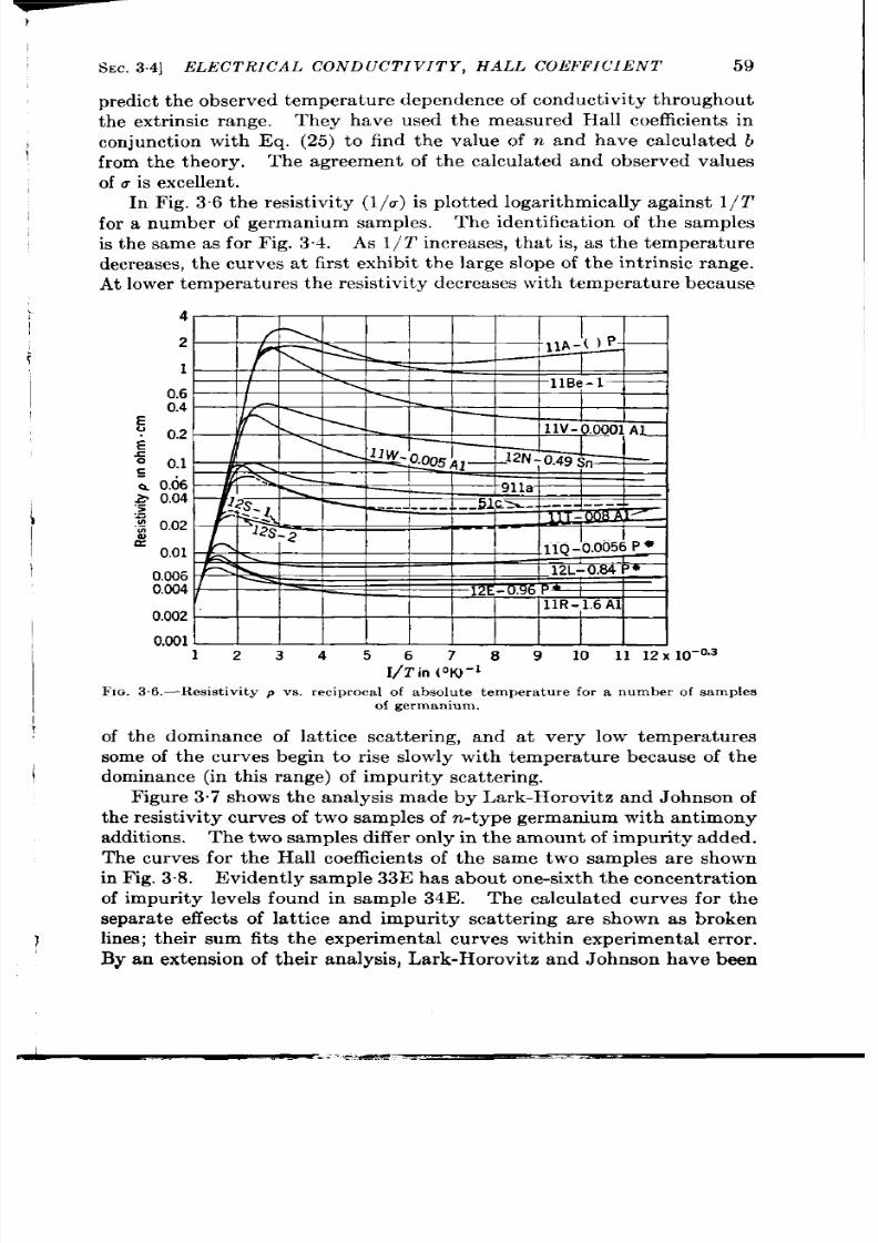
SEC. 3.4] ELECTRICAL CONDUCTIVITY , HALL COEFFICIENT
59
pr edict t he obser ved t emper at ur e dep n den ce of con du ct ivit y t hr ou gh ou t
the ext r insic range. They have used the measured Hall coefficien ts in
conjunct ion with Eq. (25) to find the va lue of n and have calcu la ted b
from the theory. The agreement of the ca lcula ted and observed va lues
of u is excellen t .
In Fig. 36 the resist ivity (l/u) is plot t ed loga r ithmically against 1/2’
for a number of germanium samples.
Th e iden tifica tion of t he samples
is the same as for Fig. 3.4. As l/T increases, tha t is, as the tempera ture
decrea ses, th e cu rves a t fir st exh ibit t he la rge slope o th e in t r insic ra nge.
At lower t emper at ur es t he r esist ivit y decr ea ses wit h t emper at ur e beca use
4
2
1
I k
0.6
I
llBe-1
0.4
l—
\ _
I I
: 0.2
z
c 0.1
[
~ 0.06
~ 0.04
.=
al
a 0.01
0.006
0.W4
~ —
,
0.002
llR-1.6A1
0.001-
12345678 910
11 12x 10-0”3
I/Tin (’IQ-l
FrQ. 3.6.—Resistivity p vs. r ecipr oca l of a bsolu te t emper a tu re for a n umber of samples
of germanium.
of the dominance of la t t ice sca t ter ing, and at very low tempera tu res
some of the curves begin to r ise slowly with tempera tu re because of the
dom in an ce (in t his r an ge) of im pu rit y sca tt er in g.
Figure 3.7 shows the analysis made by Lark-Horovit z and J ohnson of
t he r esist ivit y cu rves of t wo samples of n -t ype germa nium wit h a nt im on y
addit ions. The two samples differ only in the amount of impur ity added.
The curves for the Hall coefficien ts of the same two samples a re shown
in Fig. 3.8. Eviden tly sample 33E has abou t one-sixth t he concen tra tion
of impur ity levels found in sample 34E. The calcu la ted curves for the
sepa ra te effect s of la t t ice and impur ity sca t t er ing are shown as broken
lines; their sum fits the exper imen ta l cu rves with in exper imenta l er ror
By an extension of their analysis, La rk-Horovitz and J ohnson have been

60
PROPERTIES OF S EMICONDUCTORS
[SEC.
34
0.10
Owl
.
/
‘.
u
,.
,/ -
Mtice-
-
/
o 1 2 3
4.
5 6 7X1O-3
I\Tin (°K)-]
F IZ. 3.7.—An alysis of r esist ivit y a t low t emper at ur es for n -t ype germa nium. Th e
sum f la tt ice a nd impu rit y cu rves fit t he cor respon din g exper im en ta l cu rves wit hin
experimental error .
— exper imenta l curves
calculatedpr, p~ for 33E
——— calculatedp~, pL for 34E
FIG,
3%-
21XI
100— — — — —
@Xl
33E (4Sb)
~’w
;
20
—
u
E 10
ME(11Sb)
56
:4
-
E
82
.
+1
x
+
27 (4L
)
:0.6
$ 0,4
s
0.2
0.1
1
2
3 6 7X10”3
l/2’
in @()~
-Mewuwd Hall coe5cient IN in germaniumsamplesvs. reciprowd
temperature.
of abdu te
\
I
i

SEC.3.5]
CONSTANTS OF S ILICON AND GERMANIUM
61
able to fit t he resist ivity curves over the whole t emperature range,
inclu@g the in t r in sic par t .
In ig. 3.5 the cu rves marked I(p) and II(P) show the dependence of
resist ivit y on tempera ture for two samples of p-type silicon .
Again
t hr ee ch ar act er ist ic r egion s a re sh own .
Th e ch ief qu alit at ive differ en ce
between these curves and the corresponding curves for ger an ium
samples is the more rapid increase of resist ivity with cooling a t low
tempera tu res. As is eviden t from the curves of the Hall coefficien t for
the same two samples (Fig. 3“5) th is increase is pr incipa lly a resu lt of the
decrease in n , with cooling and is lit t le a ffect ed (con t ra ry to the case of
germa nium) by t he dom in an ce of im pu rit y sca tt er in g a t low t emper at ur es.
Measurement s of u and R as a funct ion of t empera tu re for silicon
and germanium have been made a t Purdue Univer sity and a t the Uni-
ver sit y of P en nsylva nia . 1
Th e cu rves r epr odu ced h er e wer e pr ovided by
the Purdue group. 2
3.5. Cha ra cter ist ic Consta nts of Silicon and Germa nium.
Impurity
Activa~ion Energies. —Am ong t e physical quant it ies ch ar acter ist ic of
silicon and germa t ium and of their impur ity con ten t a re AEI and AEZ,
represen t ing, r espect ively, the depth of dona tor levels below the nea r ly
empty band in the case of an n-@pe ext r in sic semicon du ct or , and t he
heigh t of the acceptor levels above the nea r ly fu ll band in the case of a
p-t ype ext rin sic sem icondu ct or .
These quant it ies may be ca l ed the
impu rit y a ct iva tion en er gies.
As will be shown in Sec. 4“3, these quant it ies a re of impor t ance in the
diffusion (th ick-ba rr ier ) t heor y of rect ifica t ion a t a ll frequ en c es. Th ey
en ter a lso in to the diode (th in-bar r ier ) theory of rect ifica t ion in the case
of h igh (micr owa ve) frequen cies, as sh own in Sec. 4“6.
The impur ity act iva ion energy may be found, as shown in the
pr eviou s sect ion , fr om t he depen den ce of Hall coefficien t on t em per at ur e
a t low tempera tu res. In the case of germanium the magnitudes of AE,
and AEZ are so small tha t they a re not easily measured by the slopes of
t he cu rves of log,O
IR I vs. I/ T , as is seen
from Fig. 3“4. It will su ffice
for ou r presen t pu rposes, however , t o know tha t All, and AE, a re small
compared with k T in t he case of germani m.
In the case of silicon the impur ity ac iva t ion energy is defin it e and
measu rable, as can be seen from the plot of the Hall coefficien t s in
Fig. 3.5. For the two samples (both p-type) plot t ed there we obta in
AEZ = 0.081 ev for sample I and AEz = 0.074 ev for sample II. Both
1K. Lark-Horovitz ,A. E. Middleton, E. P. Miller , and I . Walerstein,“Electr ical
Propert iesof GermaniumAlloys, I . Electr ical Conduct ivi ty and Hall Effect ,” Phys.
Rsu .,69, 258 (1946); and F. Seitz , “The Elect r ica lConduct ivity of Silicon and Ger-
manium,”NDRC 14-110,U. of Penn., Nov. 3 , 1942.
ZPrivatecommunication.

62
PROPERTIES OF S EMICONDU TORS
[SEC35.
samples I and II have unknown amounts of aluminum addit ions, the
amounts, however , being sufficien t t o give conduct ivit ies of th e magni-
tu des desir ed for silicon as u sed in r ect ifier s.
Carrier Mobi/it ie.s.-The mobility of the curren t car r iers en ters in to
the theory of rect ifica t ion at high frequencies (see Sec. 4.6). Other
factors being the same, the higher the mobility, the higher the rect ifi-
cation efficiency.
The mobility can be determined, as expla ined in Sec. 3.4, by com-
bining data on Hall coefficient and on conduct ivity. Mobility is influ-
enced both by the la t t ice and by the impur it ies.
At h igh t emper at ur es
2800
\ ,
—-—- Theoretical case
without impurity
2400
— 33 E-4 Sb
––– 34 E–ll Sb
: E
: ~ 2000
. >
.5
~- 16J30
\\
1200 “ .
\
\
N
\
\ \
800 -
.
400
i
d--L-
700
Absolute temperature in ‘K
FIG. 3.9.—Electronic mobil ity b, in germa nium a s a fu nct ion of a bsolu te t emper at ur e.
la tt ice sca tt er in g is pr edom ina nt a nd t he mobility is pr oport ion al t o
T–Jfi.
At low tempera tures the influence of impur ity sca t ter ing decreases the
value of mobility from that given by the th ree-ha lves-power law. In
Fig. 3.9 the tempera ture variat ions of mobility in two samples of ger -
manium (the same samples plot ted in Fig. 3.7) are shown and compared
wit h t he th eor et ica l t hr ee-h alves-power law for la tt ice sca tt er in g a lone.
It will be reca lled that these two samples differ only in the amount of
impurity. F igure 3.9 shows clearly the effect of impurity concent ra t ion
on mobility. At high tempera tu res the three-ha lves-power law is obeyed
for both samples; a t low tempera tures th e depar ture from the theoret ica l
cu rves is mos t p ronounced for t h e sample of gr ea t er impu rit y concen t ra t ion .

.
I
SEC.35] CONSTANTS OF S ILICON AND GERMAN IUM
63
The cont r ibu t ion to mobility from la t t ice sca t t er ing a lone may be
wr it ten a s
B,
b’ = jwi”
(31)
for n -type, with a simila r expression with subscr ipt s 2 for p-type. La rk-
Horovit z and J ohnson’ have obta ined for germanium BI = 6 X 10’ and
cm/sec
Bz = 2 X 10⁶,
where
b
is measured in — and
T
is in d egr ees Kelvin .
volt/cm
Making u se of Eq. (2o) t oget her with t he t heoret ica l expression for mea n
free path due to la t t ice sca t ter ing, it can be shown tha t
m2
( )
, %
—.— ,
ml Bt
(32)
wh ich yields mz~m 1 = 1.6 for germa nium.
Only n-type germanium and p-type silicon a re used in pract ica l
rect ifiers. Probably owing in la rge par t t o the effect ively la rger masses
of silicon holes over germanium elect ron s, t he ca rr ier mobility in p-t ype
silicon is one-th ird or less than tha t in n -type germanium. As has
a lready been men t ioned, excellence of a rect ifier depends st rongly on
magn itude of mobility. Fo th is r eason alone germanium migh t be
expect ed t o be pr efer able t o silicon .
H owever , ot her fa ct or s en ter wh ich
mit iga t e t h i cir cumst ance.
Mean Free Pa ths.—The mean fr ee pa th of the cur ren t car r iers is an
impo tan t pa rameter in the theory of rect ifica t ion .
Besides en t er in g
in to the mobility, Eq. (20), the magn itude of the mean free pa th (as com-
pa red with the th ickness of the rect ifying ba r r ier ), det ermines which of
t he sever al t heor ies of r ect ifica tion h old.
Since individual resist ivit ies, t he one ar ising from la t t ice and the
other from impur ity sca t t er ing, add to give the tota l resist ivity, t he
cor responding mean free pa ths add by the reciproca l law
(33)
where 1Xand lL a re the mean fr ee paths due respect ive y to impur ity and
t o la t t ice s ca t t er ing.
In llg. 3.10, 1, and lL a re plot ted as a funct ion of t empera tu re for
th ree samples of germanium. The plot for z. k t he same for all samples,
whereas the values of 11, of cour se, depend on the amount of impu ity.
The tot a l 1, exper imenta lly determined, is a lso plot ted in each case. For
most samples of germanium usefu l in rect ifiers 1 will lie in t he neighbor -
hood of from 10–s cm to 5 )( 10-G cm.
1Privatecommunication.

~
64
PROPERTIES OF S EMICONDUCTORS [SEC.36
I
Nosuch extensive analysis of data is~vailable for silicon at present , ~
but the values of the tota l mean free path may be found from Hall and
resi t ivity data . For the two samples shown in Fig. 35, we find
)
1 = 1.0 X 10–Gcmand 2.9 X 10-G cm forsamples Iand Irrespect ively. \
These values maybe regarded astypical for samples of silicon useful in
rectifiers.
Wid th oj th e “Forbid den ” Region.—The separa t ion of the near ly full
I
band from the near ly empty band, that is, the width AE of the “for -
bidden” region in Fig. 3.3, is determined by the slopes of the logl~ a or
log,O IR[ curves vs. l/Z’ inthe int r insic regions, asexpla inedin Sec. 3.4.
I thk way we find AE = 0.76 ev in the case of germanium and AE = 1.1
f
ev in the case of silicon.
6
4
‘.
-.
‘“ ‘??<Q ~,
2
:
. . . . .
s!
- ----
:1
;06 ‘ . .
~04
-..
~E.P::43 ~b)
g
+ ,$
>---- ‘?
---
-----
:02
‘+?;!l
~
...%
..:6) /
scm~n~-
--
26L
01
-.
33E—
------
. . . . . .
006
0.C4
34E
1
2 3
4
5 6
7X1O’
VTmTK)-’
FIG.
3,10.—Elect r on mean fr ee pat h s of a t ypica l group f s amples of german ium .
mean fr ee pa th due t o impu rit y sca t ter in g.
——— mean fr ee pa th du e t o la tt ice sca tt er in g (same for a ll samples).
effect ive mean fr ee pa t h due t o combina tion of two types of s ca t t er ing.
Although AE does not en ter in to the theor ies of rect ifica t ion, it is
probably of importance in the case of high-inverse-voltage rect ifiers. It
is pos ible that the existence of voltage peaks and negat ive resist ance in
the d-c characterist ics of high-voltage rect ifiers a re ascribable in par t t o ‘
the onset of int r insic conduct ion at the high power levels a t which these
effect s occu r (see Sec. 12.7).
3.6. Effect of Impurity Addit ions in Silicon and Germanium.-If it
were possible t o obta in per fect ly pure silicon and germanium, so that
even a t normal tempera tures (= 300”K) conduct ion w uld be purely
int rinsic, t he con du ct ivit y y would be ver y low.
By ext rapola t ion of the
int rin sic pa rt s of t he r esist ivit y cu rves we find t ha t t he int rin sic con tr ibu-
t ion to conduct ivity at 300”K is about 10–6 mho/cm for silicon and
10-’ mho/cm for germanium. In either case the smallest observed con-
duct ivity for pure materia l is of the order of 10–’ mho/cm.
In studying the proper t ies of these semiconductors much work has

SEC.3.6]
EFFECT OF IMPURITY ADDITIONS
65
been done on the effect s of va r ious addit ion agent s. It is a st r iking f ct ‘,
t ha t m ost im pu rit ies h ave t he effect of m akin g silicon ext rin sica lly p-t ype
a nd german ium ext rin sica lly n -t ype.
Th er e a re some n ot able except ion s
to th is ru le, however . Thus boron , a luminum, gallium, and oxyge
pr odu c st ron g p-t ype con du ct ion in s licon and wea k p-t ype con du ct io
in germa nium, wh er ea s n it rogen , ph osph or us, a rsen ic, a nd a nt imon y give
st ron g n -t ype condu ct ion in germanium an d at least ph osph or us pr odu ces
n -type conduct ion in silicon . It is a genera l ru le tha t elemen t s in the
th ird column of the per iodic t able t end t o p oduce p-type conduct ion ,
and element s in the fift h column tend to produce n-type co duct ion in
both ma ter ia ls .
It is not difficu lt t o under stand the reasons for th is ru le. Silicon and
germanium are in the fou r th col mn of he per iodic table. They have
fou r va lence elect rons and form tet r ahedra l bonds (diamond la t t ice).
An elemen t with t h ree va lence elect rons and of about the same a tomic
dimensions would be expected to be able to subst itu t e for a silicon or
germa nium atom in t he la tt ice, a ccept in g an elect ron from t he filled band
in order to complet e the tet r ahedra l bond. A hole wou ld thus be left
in the filled band and would then either become bound to the impur ity
ion or wou ld, as a resu lt of therma l excita t ion , fr ee it self and wander
th rough the la t t ice, act ing as a fr ee ca r r ier .
On the other hand an atom with five va lence elect rons (fifth column)
would give up an elect ron as a resu lt of the t et r ahedra l binding.
This
elect ron would either be bound t o the ion or fr ee it self t o the conduct ion
band.
Other element may have ana logous effects. For example, oxygen ,
being very elect ronega t ive, wou ld be expected to act as an acceptor and
produce hole conduct ion , as in fact it probably does. It probably, how-
ever , en ter s t he la tt ice in ter st it ia lly r at her t ha n su bst it ut ion ally.
It is a remarkable fact tha t a lmost all impur it ies in t roduced in to pure
silicon or germanium give r ise to ext r insic conductors of about the same
a ct iva tion en er gy (differ en t, h owever , for t he t wo sem icon du ct or s). Th is
and the fu r ther remarkable fact tha t th is energy in every case is very
small (compared with the band sepa ra t ion) was expla ined by Bethe. 1
He po n ted ou t tha t the impur ity ion will a t t r act the fr eed elect ron or
hole and bi d it in a cou lomb field, independ n t o the ion and dependen t
on ly on t he dielect ric con st an t of t he sem icon du ct or .
Let us, for example, consider the case of a t r iva len t impur ity such as
a luminum. If the hole it produces just succeeds in freeing it self, it
wou ld have an energy at the top of the normally filled band. If, on
the other hand, the hole is bound to the impur ity ion , it s energy will be
1H. A. Bethe , “Theory of the BoundaryLayer of Crys ta l Rect i fie rs,”RL Repor t
No. 43-12,NOV.23, 1942.
!
66
PROPER TIES OF S EMICONDUCTOR S
[SEC.3.6
less and the corresponding acceptor level will lie above the top of the
filled band by an amount determined by the binding energy of the hole.
Classica lly the hole will descr ibe an orbit about the negat ively charged
ion and its energy can be determined by the Bohr formula for the energy
of the elect ron in a hydrogen atom.
The in teract ion potent ia l ener y
in the present case will be e2/cr , where c
is the permit t ivity of the semi-
conductor . The Bohr formula must the efore be modified by replacing
e (the elect ronic charge) by e/~. This modificat ion leads to the
energy
AEt = – ‘)
(34)
where
Ru
is the Rydberg energy (13.5 volt s) and
n
the quantum number
(n=l,2,3, ””
.). The acceptor level therefore lies an amount AEz
According to Eq. (34) there hould be an infin ite ser ies of levels,
n=l tom. This, however , is not actua lly the ase because of the large
dimensions of the orbits obta ined for n >1.
Already for n = 1 the
rachus of the orbit is c/co t imes the Bohr radius, or 7 X 10–s cm for
c/q = 13. The radius increases as n’ and is therefore 3 X 10⁻⁷ cm for
n = 2. With 5 X 10~la impurit ies per cubic cent imeter , their mean
distance apart is about 7 X 10⁻⁷ cm. A hole tha t is 3 )( 10–7 cm from
a ce ta in negat ive ion is therefore just as near to a neighboring ion and
is not subject to the coulomb force of one ion , but ra ther to the forces
of many. This means tha t the discrete sta te n = 2 does not actua lly
exist bu t is a bsorbed in t he con tinu um.
An ion , t her efor e, pr odu ces on ly
one level and th is is separa ted from the band by the energy AE7 of
Eq. (34) with n = 1. The energy AEZ on this basis turns out to be
0.08 ev which s about the value observed in the case of sili on . From
thk discussion it is eviden t tha t the posit ive ions, instead of producing
addit ional levels (n = 2, 3, . c
o), actually ra ise the upper limit of the
filled band. This effect should lower AE, to perhaps 0.04 to O.O6 ev.
This discussion ha been illustrated by an example of a negat ive ion
and posit ive hole (p-type ex rinsic semiconductor ). The same argu-
ments apply to the case of a posit ive ion and an elect ron except tha t now
the elect ron level lies just below the conduct ion band. The est imated
value of AE1 is, however , the same as AEZ.
Exper imenta lly, AEI (or AEz) is 0.02 ev or less in the case of ger -
Bethe’s theory thus gives the
right order of magnitude although the difference between germanium
and silicon is n ot expla in ed.
This sect ion concludes with rem rks concern ing the efficiency of
va riou s a da lt ion a gen ts.
It has been found that a lthough many addit ion agents will produce
SEC. 3.6]
EFFECT OF IMPURITY ADDIT IONS
67
conduct ivit ies of t he desir ed or der (10 t o 100 mho/cm) only a few pr odu ce
good stable rect ifier s. Thus, aluminum and boron have been found to
be best for silicon, and phosphorus and ant imony are super ior for ger -
man ium. 1
Boron has the remarkable proper ty (unique among all addi-
t ion agents) tha t , in the case of silicon, an ext remely small amount
(= 0.001 per cent ) is sufficient t o pr oduce th e desir ed conduct ivit y.
Aluminum and beryllium added to silicon in small quant it ies have the
desirable fea tu re of increasing the hardness and toughness of the ingot .
Fur thermore, they serve to improve the resist ance to burnout . Accord-
ingly, the combinat ion boron-beryllium in approximate per cen t by
weight , 0.002 and O.O2 respect ive y, added to pure duPont silicon, was
k
found at Radiat ion Laboratory to produce super ior ingot s. In this case
almost all the conduct ivity is supplied by the boron.
:
It is notewor thy that the impur ity addit ions best for silicon are as a
genera l ru le worst for germanium; the rever se is a lso t rue. 1 Thus
ilicon, as us d for r ect ifier s, is a lways p-t y e (h ole con duct or ), wh er eas
germanium is a lwa ys n -t ype (elect ron con du ct or ).
I Th es e r emar ks d o not a pply t o h igh -in ver se-volt age r ect ifier s (s ee Ch ap. 12).

CHAPTER4
THE SEMICONDUCTOR—METAL CONTACT
This chapter t rea ts of the process of rect ifica t ion at the contact
bet ween a meta l an d a sem icon du ct or .
The ba r r ier -r ect ifica t ion process
will be descr ibed qualita t ively and it will then be shown how he condi-
t ion s n ecessa ry for r ect ifica tio a re obta in ed at a met al-sem icon du ct or
contact.
Th e
t ine
qua non for rect ifica t ion is the existence of a barr ier
layer at the contact . The st ructu re of th is layer and its modifica t ions
are examined in some detail.
F inally the special circumstances of
r ect ifica tion a t h igh fr equ en cies a re con sider ed.
4.1. Ba rr ier -la yer Rect ifica tion .-Th e r ect ifica tion pr ocess in cr yst als
takes pla ce in t he immedia te vicin it y of t he met al-sem icon du ct or con ta ct ,
Metal 1 Insulator
Metal 2
Metal 1 Insulator Metal 2
(a) before contact
(b)
just after contact
Metal 1 Insulator Metal 2
(c) equilibrium established
FIG.4 .1 .—Format ion of a rect ifying bar r ie r between two meta ls of d iffe ren t work funct ion .
in fact , with in a few hundred or thousand atomic diameters of the
con tact sur face. In this region th ere exist s a potent ia l bar r ier or “hump”
of potent ial energy. Rect ifica t ion is believed to be a result of the asym-
metr ica l distor t ion of th is hump by th e applied potent ia l.
Semiconduct ion is not at all essent ial for rect ifica t ion and the on ly
excuse for the use of semiconductors is tha t the required barr ier is easily
and naturally formed at a meta l-semiconductor c ntact Under cer ta in
condit ions, h owever , a similar potent ia l barr ier may be formed between
two m tals that differ in surface work funct ion; the barr ier will then
rect ify. Sin ce this process is some~vhat easier t o understand than meta l-
sem icon du ct or r ect ifica tion , a br ief sket ch of it is given first .
1 The term
rect ifica t ion ‘‘ implies a cu rmnt-volt age cha ract er is tic a symmet r ica l
with respect to the volta ge, tha t is, 1( +v)l >> II( —u) This condit ion applies also in
t h e ca se of fr equency conver sion .
6s

SEC. 4.1]
BAE IER-LA YER RECTIFIC.4 TION
Figu re 4. la sh ows t he cu stom ar y pot en tia l-en er gy
69
diagraml of two
meta ls of differen t work funct ions not in con tact . Let us suppose tha t
between them there is a th in wall of a crysta lline insula tor with filled and
empty elect ron ic bands. Immedia tely a ft er con ta t has been made the
situa t ion is as shown in Fig. 4. lb. There will resu lt a net elect ron f!ow
from meta l 2 to meta l 1 because there a re more elect rons nea r the top
of the ba rr ier in meta l 2 than in meta l 1. This flow will persist until a
sur face double layer of ch ar ge is esta blished; th is double la yer depresses
the elect ron levels of meta l 2 rela t ive to those of meta l 1, bringing the
tops of the Fermi distr ibu t ions of the two meta ls to the same level. At
th is poin t no fu r ther net flow occurs and we have a sta te of equilibr ium
(Fig. 41C).
The result of applying an ext ,ernal volt age (smaller in magnitude
than the work-funct ion dif erence) in the direct ion which ra ises the
(a) Voltageapphedin
(b) Voltageapphed in
forward direction
back dtrection
FIG. 4.2.—Rectification at a metal-metal contact.
elect ron levels in meta l 2 rela t ive to those of meta l 1 is shown in ig. 4.%;
the result of applying a voltage in the opposit e direct ion is shovn in
Fig. 42b. In either case there s no change in the heigh t of the ba rr ier
as viewed from meta l 1 (meta l of h igher work funct ion) bu t the height
of the ba rr ier , viewed from meta l 2 (meta l of lower work funct ion ),
increases linear ly with applied volt age V. Thus in neither case will
there be a change in the number of elect rons flowing from meta l 1 across
the bar r ier to meta l 2, bu the flow from meta l 2 to meta l 1 (and hence
the net cu r ren t ) does va ry with voltage. If the energy dist r ibut ion of
elect rons (tha t is, the number of elect rons per unit energy range) in
meta l 2 wer e constan t fo energies above the Fermi sur ace, th ere would
be n o r ect ifica tion , a nd t he con ta ct wou ld be ohmic (cu rr en t pr opor tion al
to voltage). This elect ron dist r ibut ion , h wever , is not , in fact , on -
stant , but nea r ly exponent ia l (Be! izmann law); hence the curren t is
nonlinear with voltage, the barr ier is nonohmic, and rect ifica t ion is
possible.
From the above example it can be seen tha t la rge net cur re~,t s flow
1F. Seitz ,The
Mod ern T heory oj S olid s, McGr aw-H ill, N ew Yor kl 1940, Sec. 26.
L– —— .
70
THE S EMICONDUCTOR—METAL CONTACT
[SEC.4.2
when the elect ron energy levels of meta l 2 (low work funct ion) a re ra ised
rela tive to th ose of meta l 1 (h igh wor k fun ct ion ) by th e applied poten tia l,
tha t is, by making meta l 1 anodic and meta l 2 ca thodic. A voltage so
applied is said to be in the “forward”
direct ion; an opposite volta ge is
said to be in the “reverse” or
“block ing” d ir ect ion .
Th e simple example given r edu ces t he gen er al pr oblem of r ect ifica tion
to its ba re essent ia ls. The more in terest ing case, however , in which
one of the meta ls is replaced by a semiconductor and the insula t ing layer
is absent , differs on ly in degree and not in kind from this simple case.
The simple case, however , is not en t irely academic in in terest . It
should be possible to make meta l-insula tor-meta l r ect ifiers with much
sma ller spr ea din g r esista nces t ha n m et al-sem icon du ct or r ect ifier s h ave,
con sequ en tly givin g gr ea ter r ect ifica tion efficien cy a t h igh fr equ en cies
(see Sec. 4“6).
At tempt s t hu s fa r t o con st ru ct wor ka ble met al-in su la tor -
meta l rect ifiers have not been successfu l, but in view of their possible
a dva nt ages fu rt her r esea rch is desir able.
4.2. Format ion and St ructu re of the Bar r ier Layer .—It was shown in
the preceding sect ion how rect ifica t ion is accomplished with the aid of a
bar r ier layer between mater ials of differen t work funct ions. The nature
of the barr ier layer formed in the vicin ity of a meta l-semiconductor
cen t a ct , will n ow be examin ed.
The equilibr ium between the elect rons of a meta l and those of a
semiconductor is governed by the equality of the elect ron chemica l
potent ia l in the two mater ials. This condit ion , it has been noted,
require tha t a l elect ron levels in the semiconductor be depressed by the
amount e~~ rela t ive to thos of the meta l.
Expressions for e~~ are
given by Eqs. (3.14) to (3.18) for the va rious cases of in terest .
In th is chapter we shall not be concerned with in t r insic semiconduc-
t ion since, in the case of silicon and germanium, th is occur s only a t
eleva ted tem pera tu res and would in any ca se result in poor rect ifica tion
because of the equal numbers of elect rons and holes. For ext r insic semi-
conduct ion an approximat ion useful for the presen t purpose s found by
ignor ing term of order k T in e~m, since these terms are small compared
with the con tact potent ia l difference in all cases of in terest . Thus, from
Eqs. (3.15 to 3.18) we get
(1) n -type ext r in sic (all va lues of n ,),
—ebzm = —e@O= x2 — x. = Wz— x.;
(1)
(2) p-type ext r insic (all va lues of n ,),
‘e@m ~
—dm = X4 — x. = w= + All — xm.
(2)
(See F ig. 3.3 for an explanat ion of the symbols used.) ~erms in AEI
!,
,f
[
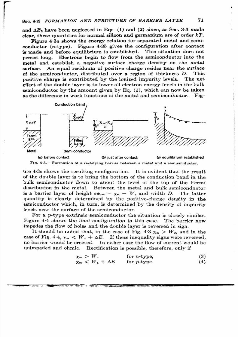
6
%C. 4.2] FORMATION AND S TRUCTURE OF BARRIER LAYER
71
and AE2 have been neglecx ed in Eqs. (1) and (2) since, as Sec. 3,3 made
clea r, t hese quant it ies for normal silicon and germanium a re of or der kT .
Figure 4.3a shows the energy rela t ion for separa t d metal and semi-
conductor (n-type). Figure 4.3b gives t he con figu ra tion a ft er con ta ct
is made and before equilibrium is established. This situat ion does not
pemist long. E lect rons begin to flow from the semiconductor in o the
metal and establish a nega t ive surface charge density on the metal
surfa e. An equal residuum of posit ive charge resides near t he surface
of the semiconductor , dist r ibu ed over a region of thickness D. This
posit ive charge is cont r ibuted by the ionized impurity levels. The net
effect of the double layer is t o lower all elect ron energy levels in the bulk
semiconductor by the amount given by Eq. (1), which can now be taken
as t he differ en ce in wor k fun ct ions of t he met al a nd sem icon du ct or .
Flg-
brduction band
/
z
Metal
Semiconductor
(a) before contact (b) just after contact (c) equilibrium established
FIG.4.3.—Format ion of a r ect ifying ba r rier between a met a l and a s emiconduct or ,
u r e 4.3c shows t h e r esu lt in g con figu ra t ion .
It is evident tha t the result
of the double layer is t o bring the bot tom of the conduct ion band in the
bulk semiconductor down to about the level of the top of the Fermi
dist r ibut ion in the meta l. Between the meta l and bulk semiconductor
is a barr ier layer of height e~~ = x~ — JVz and width D. The la t t er
quant ity is clea r ly determined by the posit ive-charge density in the
semiconductor which, in turn, is determined by the density of impurity
levels n ea r t he su rfa ce of t he sem icondu ct or .
For a p-t ype ext rinsic semiconduct or t he situa tion is closely similar .
Figure 4.4 shows the final configura t ion in this case. The barr ier now
imp des the flow of holes and the double layer is reversed in sign.
It should be noted that , in t he case of Fig. 43 X* > Wc, and in the
case of Fig. 4.4, x~ < W. + AE. If these inequality signs were reversed,
no barr ier would be erect ed. In either case the flow of current would be
unimpeded and ohmic. Rect ifica tion is possible, t her efor e, only if
x. >
w=
for n-type,
(3)
x.< W*+AE for p-type. (4)

72
THE SEMICONDUCTOR—METAL CONTACT
[SEC.4.2
It is clear that the same metal and the same semiconductor with
different types of impur it ies a re capable of sa t isfying both Eqs. (3) and
(4). This deduct ion is in accord with the observed fact tha t both silicon
and germanium, proper ly “doped,”
a re capable of giving n-type or
p-t ype r ect ifica t ion in con jun ct ion wit h t he same metal.
Rect ifica t ion is accomp ished in much the same manner as by the
bar r ier between the two metals of differen t
work unct ions discussed i the preceding
sect ion . F@r e 4.5a sh ows t he con figur at ion
of the meta l-semicon uctor bar r ier when a
volt age is applied in the forward direct ion
(direct ion of easy flow). The heigh t of the
bar r ier , viewed from the meta l, is st ill given
Metal
Semiconductor
by o,, the contact potential difference. Thus
(P.type)
t he n umber of elect ron s t ra ver sin g t he ba rr ier
FIG.4.4.—Barrier between a
from metal to semiconductor is a constan t
metal
and a
p-type semi-
independen t of the applied volt ages. On the
conductor.
other hand, the elect ron levels in the semi-
conductor have been ra ised by the amount eV, where —V is t h e app lied
volt age; h en ce t he h eigh t of t he bar rier , viewed fr om t he sem icon du ct or ,
has decreased by eV. The “slack” has been taken up by a decrease
in bar r ier space charg because of a flow of elect r ons in to the bar r ier .
Sin ce t he elect ron en er gy dist ribu tion in the s emiconductor is exponen t ia l
above the bot tom of the conduct ion band, the elect r on cur ren t from semi-
conductor to met al in cr ea ses expon en tia lly wit h V.
+&
c
o—— +
—~oe m
4V
t
FIG. 4.5.—Rectificat ion by a
metal-semiconductor barrier.
F igure 4.5b sh ws the configura t ion of the bar r ier with a voltage
applie i the blocking direct ion . Again the bar r ier height , viewed from
the meta l side, and also t he elect ron flow fr om met al t o sem icon du ct or
have not been changed by the applied volt age. The bar r ier height,
viewed fr om t he sem icon du ct or , has in cr eased and t he elect ron flow fr om
sem icon du ct o t o m et al h as decr ea sed.
Let us now examine in more deta in t he st ructu re of the bar r ier layer .
1
For the following theory of a natura l “dielect r ic” barrier , see fur ther , H. A.
SEC.4.2] FORMATION AND S TRUCTURE OF BARRIER LAYER
73
The shape of the barr ier is rela ted to the space charge by Poisson’s
equation,
dE
— = : (n+ – ?L),
dz
(5)
where E is the elect r ic field intensity, c is the permit t ivit y of the semi-
conduct or , e is the elect ronic charge, and n+ and n- a re, respect ively, the
number densit ies of posit ive and negat ive charges. The discussion will
be confined to an n-type extr insic semiconductor . Then n_ is taken
to be the number density of free elect rons and n+, the number density
of ionized donat ors. The not at ion of Fig. 4.5 is used: e~o is t he differen ce
of work funct ions, and the height of the barr ier as viewed from the
metal. If e@is the potent ia l nergy of an elect ron and – V is t h e applied
volt age, t hen
(6)
A potent ia l of order kT / e or la rger above the potent ia l of the bulk
semicon uctor is sufficient t o remove near ly all the elect rons from the
dona tors and to reduce the elect ron density to a value small compared
Now kZ’ e is only 0.026 volt a t room
tempera ture, very small compared with the potent ia l difference 00
(= 0.5 volt ). Therefore, over most of the potent ia l curve of the barr ier
it may be assumed tha t + = N and n– = O, where N is the dona tor
density. Thus the charge density in the barr ier is constant and equal
t o Ne. Poisson’s equat ion then simplifies to
d’4 = _,
N
@e
(7)
Now, Eq. (7) is in tegra ted with t he boundary condit ions,
@=v, ~=o
atx=D;
(8)
4=00
atz=O;
where D is the thickness of the barr ier , tha t is, the layer in which the
cha rg of t he donat ors is not neutra lized by elect rons.
Thus,
@= V+~(D–z)2
(9)
with
[ 1
D = 2,(4, – v) ‘i
eN “
(lo)
Bet he, “Th eor y of t he Bou nda ry La yer of Cr yst al Rect ifier s,” RL Repor t No. 3-12,
NOV.23, 1942.

I
74
THE SEMICONDUCTOR—METAL CONTACT
[SEC.42
Asanexample, if V = O, @O= 0.5 volt , e = 13c0, and N = 5 X 18”
cm–3, we fin d that
D = 1.2 X 10⁻⁶ cm,
(11)
which is comfor tably large in compar ison with the intera tomic distance.
The value assumed her e for N, 5 X 10’s cm–3, is fa ir ly typica l of repre-
sen ta tive samples of silicon an d germa nium.
The value 13 assumed for
~/eOis in accord with the spect roscopic dataz for silicon and cannot be
much differen t in the case of germanium.
The value of the potent ia l
cliffer en ce (I#Io= 0.5 volt ) is in a ppr oxim at e a ccor d wit h m ea su rem en ts of
Meyerhof’ for silicon against tungsten . Var ia t ions in these assumed
value will not in any case change the resu lt much because of the square-
root dependence of D.
It is evident , therefore, tha t a “natura l” barr ier layer will be of the
order of magnitude of 10–6 cm thick in the case of silicon and germanium.
As will be seen la ter , a bar r ier of a lmost th is th ickness is needed in order
t o a ccou nt for obser ved ba rr ier ca pa cit an ce.
Image Force.—The quant ity o gives only the potent ia l of an elect ron
in the elect rosta t ic field of the sur face.
It oes not t ake into accoun t
the image for ce act ing on the elect r on . Including the image force, the
potent ia13 is
(12)
With the constan ts as chosen, the maximum of the potent ia l W occurs
close to the meta l su r face, tha t is, a t a distance z << D. I f X2is neglected
in Eq. (9), the maximum of W is folmd to lie a t
and has a value,
‘m= ‘Q-r%)= ‘0-(2-)’
(13)
(14)
for the case of zero bias (V = O). For the values of the constan ts
a s above,
m = 0.05D = 6 X 10–s cm,
;. = 0.40 volt .
It is seen that xJ D is small; h en ce t he image for ce does n ot ser iously
affect the poten t ia l ba rr ier . This resu lt , however , is in t imately con-
1 J . F . Mullaney, Phys. Rev., 66, 326 (1944).
2W. E . St eph en s, B. Ser in , a nd W. E . Meyer h of, P hys. Ret i., 6 9, 42 (1946).
3See, for example, F . Seit z, T he M od erm T heory of S olid s, McGraw-H ill, New York,
1940, pp. 162, 163.

SEC.
4.2] FORMA TION
net t ed with he high
AND STR.5’CT URE OF BARRIER LAYER
75
dielect r ic constant chosen, which has the effect
of increasing the th ickness of the bar r ier layer [Eq. (10)] and reducing
the image-force lower ing [Eq. (14)]. Indeed, were it not for such a high
dielect ri const ant , r ect ifica t ion by a natura l bar rier layer would be ver y
poor , if n ot impossible.
Na tu ra l VS.
A rti$cial Ba rr ier s .—Th s con clusio does not , of cou rse,
ru le out the possibility of an ar t ificia l bar r ier layer .
In fact there is
reason to believe that the density of dona tors is somewhat reduced
below the bulk value near the sur face of the semiconductor in the case of
modern silicon rect ifier s. The following sect ion t rea t s the possibility
of t his d epletion layer. Such a layer would have the desirable proper ty
of increasing the thickness of the ba r ier (as 1/@) and reducing the
effect -a lways undesirabl~of image for ce.
Fur thermore, it is not a t
all cer ta in that t her e is not a sur face layer o some foreign mater ia l, such
as oxygen or quar tz, between the meta l and semiconductor .
Such a
layer would at least change the work funct ion of the semiconductor and
might even be thick enough to provide a substant ial bar r ier .
How-
ever , as Seit z 1 has pointed out , quar tz does not possess any elect r on ic
energy ban s near the conduct ion band of silicon, and thus elect rons
cou d penet ra te on]y by the “tunnel” effect . A quar tz layer as th in s
10–7 cm would be pr ct ica lly impe et rable to elect rons. On the other
hand, a layer I&’ cm thick is negligible compared with the natura l
la yer a lr ea dy pr esen t (10–6 cm ).
It seems rea onable, therefore, t o conclude that the barr ier layer in
silicon and germanium is natura l in the sense that it consists of the
mater ia l of the semiconductor , but possibly artificial in the sense that
the concen tra t ion of donator levels may be somewhat less than in the
bulk semiconductor .
Ca pa .da nce oj t he Barr ier Layer .—When a n a lt er na tin g field is a pplied
to the contact , the bar r ier is a lt ernately charged and discharged by the
flow of elect rons fro the semiconductor in and ou t of the bar r ier . Let
us assume that t ime effect s r esult ing fr om recombinat ion and ion iza t ion
of the donator s can be neglected.
They cer t a in ly can be neglected if
it is assumed that the dona tor s ar e completely ion ized in the bulk semi-
conductor . Their neglect is approximately valid in any case at low
frequencies. (The h igh-frequency case will be discussed in Sec. 4.6.)
For small amplitudes of the applied voltag the bar r ier act s as a con-
denser wit h capacit ance
C = –A:;,
(15)
1
where A is the a rea of the con tact , q is the tota l sur face charge, and – V
1F .
“The Pr inciples of Cr ys al Rect ifier s,” N-DRC
14-102, U . of P en n., J u ne 10, 1942.
76
THE SEMICONDUCTOR-METAL CONTACT
[SEC.42
is the applied voltage, ‘I’hesur fa cechargeqisgiv enby
q = NeD(V),
(16)
wh er e t he t hickn ess D depends on the applied poten ia l —V in accord-
ance with Eq. (10). Then,
(17)
which incidenta lly is the same as the capacitance of a para llel-pla te
con den ser of a rea A and th ickness D.
This capacitance effect ively shunts the nonlinear resist ance of the
bar r ier . It~value is not constant with applied potent ia l. In fact , from
Ilqs. (10) a nd(17)j
(7.
d- v“
(18)
Com parison oj Theoretical and Experim en tal Barrier C’apacitance.—
easurements of C provide the best exper imenta l data for the bar r ier
thickness D. There ar e two genera l methods for measur ing C. One
is a direct measurement of the impedance of the rect ifier . The bar r ier
c pacitance is then in fer red from the impedance, suitable account being
t aken of such ext ran eous effect s as t he wh isker inductan ce, st r ay capaci-
t ances, et c. These measurements a re usually made at frequencies of
the order of magnitude of 10 Me/see, since it is easier to take accoun t
of ext ran eou s im pedances at fr equencies of th is or der than at fr equencies
in the microwave range. A common techniqu is to measure the imped-
ance of a crysta l car t r idge just befor e and then aft er contact is made
between t he wh isk er a nd sem icon du ct or .
The second method assumes the equivalent cir cuit of Fig. 2.10 for
t he r ect ifier and com par es low-level r ect ifica t ion efficien cy at audio and
at microwave frequencies. F rom the difference one can compute C.
This method is descr ibed more fully in Sec. 11.5.
The two methods agree only in order of magnitude, the second method
genera lly giving lower values of con tact capacit ance than the fir st
The difference is probably due to relaxat ion effect s in th barr ier (see
Sec. 4 .5).
In one case’ a ft er the capacitance of a silicon-tungsten con ta t had
been determined by the br idge method at zero bias and at 14 Me/see, the
diameter of the con tact was found to be 1.2 X 10⁻³ cm. Subst itu t ion in
Eq. (17,), assuming c = 13c,, g ve D = 2 X 10–G cm. This value is to
be regarded as an upper limit , since the computa t ion assumes that the
whole a rea of the whisker point was in in t imate ccntact with the silicon.
A. W.
Capacityin SiliconCart ridgeRectifiers,”NDRC 14-140,U. of Penn.,May 1, 1943.
SEC.4.3]
DIFFUS ION AND DIODE THEORIES
77
The va lue obta ined is therefore in sat isfactory agreement with the
t heor et ica l va lu e of D, viz., 1.2 X 10⁻⁶ cm.
Measurements of var ia t ion of barr ier capacit a ce with bias do not
agree well with the square-root law,
Eq. (18). Br idge measurements
tend to show a very rapid increase of capacit ance in the forward direc-
t ion . ncreases by a factor of 100 have been observedl for silicon unit s
when t he applied v lt age was cha nged from O t o 0.5 volt (across t he whole
unit ). It sh uld be noted, however that it is xceedingly difficult t o
separa te resist ance and reactance effect s in such measurements. These
result s must be regarded as tenta t ive. The measured values at zero
bias, however , sho~ld be fa ir ly reliable, since the barr ier resist ance in
this case is large ( = 5000 ohms) compared with the barr ier -capacit ive
reactance ( = 50 ohms). At modera tely small ( = 0.5 volt ) inverse
voltages, the br idge results show a small decrease in the capacit ante,
as is to be expect ed from 13q. (18). At higher inverse voltages ( = 1.0–2.5
volt s) the capacit ance increases, but this may be a spur ious effect .
The rect ifica t ion-efficiency method does not agree with the br idge
method with regard to var ia t ion of capacit ance with bias.
In gen er al,
the former method results in a fa ir ly constant value in the inverse direc-
t ion and a small r ise for silic n crysta ls in the forward direct ion. Quan-
t it a tive compa rison wit h Eq. (18) is difficu lt , bu t, for silicon , disa gr eemen t
is not indica ted. In the case of germanium, however , observat ions
u sin g t he r ect ifica tion -efficien cy met hod h ave sh own con sider ably la rger
increases of capacit ance with forward bias than can be accounted for by
q. (18). This circumstance is helpful, however , in understanding the
nega tive i-f conduct ance of welded-cont act germanium r ect ifier s (Sees.
13.5 and 13.6).
4.3. Diffusion and Diode Theor ies of Rect ifica t ion .-A Qualita t ive
picture of barr ier -layer rect ifica t ion was presented in Sec.
“4.i.
Th e
quant ita t ive theoret ica l t rea tment is considerably affected by the va lue
assumed for the barr ier thickness.
The e are th ree dist inct cases of
in ter est , cor respondin g t o ver y t hin , in termedia te, a nd ver y t hick ba rr ier s.
A very thin barr ier ( =
10-7 cm ) offer s t he possibilit y of elect ron t ra nsit by
means of t he well-known quantum-mechanical “ t unnel” effect . 3
The fir st t h eor y of ba rr ier -la yer r ect ifica t ion , developed independen tly
in 1932 by Wilson, by Nordheim, and by others, was based on the tunnel
effect . 4 This t heory was accepted for a number of years un il it was
1 Ibid.
2R. N. Smith, “Determination of CrystalPa rameter at MicrowaveFrequencies”
(Crysta lRectifierConferen ce),Columbia U., Sept . 11,1943.
m%netic energy th roughwaveguidesbelow cut off.
4SeeA. H. Wilson, Proc. R.w. Sot., 196, 487 1932); andL . W. Nordhsin , Zm”ta ,.
F’hys., 76(7 -8 ), 434 (1932).
I

78
THE S ’EMICOND UGTOR—METAL CON TACT
[SEC.43
r ea lized t hat it pr edict ed rect ifica t ion in t he wr on g dir ect ion .
Fur ther-
more, ther e was good evidence that the bar r ier is considerably th icker
than 10–7 cm for th is and other rect ifier s.
The defect s of the tunnel theory led Mot t l in 1939 to propose a
thick-bar r ier t heory. He supposed (as we did in Sec. 4“1) that elect rons
were able t o surmount the bar r ier pr imar ily by thermal excit a t ion .
His theory was oversimplified by the assumpt ion that the elect r ic-field
intensity E was constan t in the bar r ier layer (absence of space charge).
Schot t ky’ was able t o fr ee the theory from this a rbit ra ry assumpt ion .
He considered two ext reme cases, “exhaust ion layers” and “ eserve
layer s. ” In an exhaust ion layer the impur it ies a re considered to be
completely ionized in the layer it self, a lthough not necessa r ilyy in the
bulk semiconductor . The case of an exhaust ion laver was d scussed in
S ec. 4.2. A reserve layer is complica ted by the incomplete ioniza t ion
of impur it ies and does not concern us her e, since, as was poin ted ou t in
Sec. 3.7, impur it ies a re 20 t o 40 per cen t ion ized in bulk silicon and near ly
completely ionized in bulk germanium.
Thus on ly a small r ise in
poten t ia l energy above the bulk va ue will in either case shift the equi-
libr ium to complet e ion iza t ion .
Both Mot t and Schot tky assume bar r ier s th ick compared with the
mean free path of the ca r r iers, an assu pt ion in accord with measured
va ues of 10–5 to 10–4 cm for the bar r ier th ickness in copper -cuprous
oxid e and in selen ium r ect ifier s.
Sin ce collision s occu r in t he ba rr ier , on e
is for ced t o t r ea t the flow of cur ren t in the bar r ier as a sta t ist ica l problem
involving det a iled ba lance.
A bar r ier of in termedia te th ickness (= 10-s cm), tha t is, th ick
enough
to r educe the number of elect rons penet ra t ing the bar r ier by the tunnel
effect t o a va lue small compared with the number surmount ing the bar r ier
by thermal excit a t ion yet st ill th in enough so that collisions with in the
bar r ier can be ignored, is a much simpler problem. In this case ther e
is an analogy to the mot ion of elect rons in a vacuum-tube diode. The
car r ier s must have sufficien t energy to surmount the potent ia l bar r ier
(ana logous to the work funct ion of the cathode of a diode). TheY will
then fly over the bar r ier unimpeded and make their next collision in
the meta l (ana logous to the anode of a diode). Because of these imilar i-
t ies t he t heor y of a bar rier of in termedia t e t hickn ess is commonly r efer red
to as the “diode theory.”
T he D@m ion Theory .-The th ick-ba rr ier , or iffusion , theory do s
not appear to apply to ordinary silicon and germanium mixer rect ifier s,
since, as we have seen in Sec. 4“2, their bar r ier th ickness is of the or d r of
l(FC cm, which is less than the mean fr ee path of the car r ier s. The
I N. F. Mot t ,
Proc. E@. S ot.,
A171, 27 (1939).
2W. Sehot tkyand E. Spenke ,Wiss. Veroff. S iernenewerke, 18,225 (1939).
I
I
i.
SEC. 4.3]
DIFFUS ION AND DIODE THEORIES
79
ba rr ier th ickness of h igh -inverse-v l age rect ifiers has ot yet been
determined by capacit ance measurement s, but it is difficult t o un er -
stand how a high inverse resistance can be main ta ined at applied poten-
t ia ls of 100 volt s or more (as is observed for these rect ifiers) by a bar r ier
t h~n ner th an 10–5 cm.
Th e fu ndamen ta l equ at ion gover nin g diffu sion t heor y’ is
j = elmE ~ bkT ~n.
dx
(19)
The symbo s have the following meaning: j is the cur ren t density; e, t he
absolu te va lue of the elect ronic cha rge; n , the density of fr ee elect rons
or holes ; E, the elect ric field in ten sit y; b, t he ca rr ier mobilit y; k, Bolt z-
mann’s constan t ; 2’, t he absolu te tempera ture; and z, the one-dimen-
sional space coordina t e. The plus sign holds for elect ron conduct ion
(n -t ype ext rin sic), an d t he min us sign for h ole con du ct ion (p-t ype ext rin -
sic). This law is va lid if the mean free pa th is small compared with the
distance over which the poten t ia l energy changes by n amount lcT.
The cur ren t density j is seen to be composed of two part s: one
ebnE
gives the ohmic dependence of cu r ren t on field in tensity, and the other
~ M
Z’(dn/ dz) gives
t he con t r ibut ion of cliffusion resu lt ing from the
gr adien t in ca rr ier den sit y d n/ d z.
If j = O, Eq. ( 9) in t egra tes a t once to give the usual Boltzmann law,
‘./
‘E dz
n =
const X e*m u .
(20)
For j # O, the equat ion can st ill be formally in t egra t ed, but , t o get
a usefu l resu lt , th e depen dence of
E
on n must , in genera l, be t ak n in to
account . For the case of an exhaust ion layer , E will be independent of
n , but i the case of a reserve layer it has a complica t ed dependence on n.
The la t t er dependence is given by the Poisson equa t ion [Eq. (5)], in
which we can pu n– = n. The quant ity n+ depends on n since t hey a re
r ela t ed by t he equilibr ium of t he r eact ion ,
Bound elect ron @ bound hole + free elect ron .
The rela t ion between the number of fr ee elect rons n , bound holes n+,
and bound elect rons N —
n+ (N is the donator density) is given by
nn+
—=K,
N–n+
(21)
where is t he equilibr ium co stan t of t he rea ct ion .
In the bulk semi-
conductor , n+ = n, and compar ing Eq. (21) with Eqs. (1) and (2)
1See
N .
F. Mott and R. W. Gurney, E lect ron ic Proce-wes in I on ic Cryst als, Oxford,
New
York , 1940,Chap, 5 , Eq. 30.
80
THE S EMICOND UCTOR—METAL CONTACT
[SEC.43
For tuna tely the complica t ions of a reserve layer do not appear to
apply t o germanium and silicon.
Since diffusion theory has limited, if any, applicat ion to silicon and
germa nium r ect ifier s, it will su ffice t o illu st ra te it by in tegr at in g Eq. (19)
for the specia l case (assumed by M tt ) of zero space charge in the barr ier .
This should apply, then, to an ar t ificia l insula t ing barr ier . F rom Eq. (5)
\ re see that zero space charge implies constant E. Then Eq. (19) is
in tegra ted at once to
“ [ “1
eEz
n ~) = ~& + n(0) – & e=.
(23)
At z = D we assume that we pass abrupt ly to the proper t ies of
the bulk semiconductor , so that n (D) = n(m ). Mott and Schot tky
as umedl that n(0) is given by the number density of elect rons in the
meta l a t the poten t ia l q$oabove the sur face of the Fermi dist r ibut ion
and is in depen dent of j.
Put t ing j = O and x = D in Eq. (23), we obt ain
eED
.+0
n(0) =
n(D)e
‘~ = ~(m )e kT .
(24)
Not ing that eED = I#J ,– V, subst itu t ing Eq. (24) in Eq. (23), and solv-
ing for j, we obta in
eV
——
j = [en( cc )ELE] 1– ,~+o~v).
l–e kT
Sin ce, in gen er a l,
c(~o—V)
e kr >>1,
we obt ain fin ally
C+o
~v
j’ = ebn(m )l? . e–~(ek~ – 1).
(25)
(26)
Th e expon en tia l fa ct or dominates t he wea k depen den ce of E on V, hence
Eq. (26) may be wr it t en approximately as
j = A(e”v – 1), (27)
where A and a are constants. Equat ion (2 ) is a genera l result (in the
1It hazbeen shownby R. G. Sachs,“The Difluaion Theory of CrystalRectifiers ,”
NDRC 14-129, Pu rdue U ., Sep t. 10, 1942, t hat r J (0)is not r ea lly independen tof j
and that in certaincircumstancesa term j/ev shouldbe added to the right-handsideof
% (24) whereu i s the mean thermalvelocity of the bu lk elect rons .
Thie refinement
j
will not be in t roducedhere .
SEC. 4 .3]
DIFFUS ION AND DIODE THEORIES
fir st a ppr oxim at ion) of all t heor ies of con ta ct r ect ifica t ion
com pa red with exper im en t in Sec. 4.4.
81
and will be
!f’h e Diode Theory.—If t her e is assumed a bar r ier thin compared
with the mean free path , collisions in the barr ier layer can proper ly be
neglected. The elect ron dist r ibut ion is then given by the Maxwell-
Boltzmann law based on the bulk proper t ies of the semiconductor . Thus,
if we now wr it e n for the number of ca r r ier s per unit volume in the bulk
sem icondu ctor , we h ave for
dn ,
t he number of ca r r ier s per unit volume
crossing unit area per second in the —x direct ion with vel city between
v and v + dv,
( ) ‘--
i
~“
2
dn = n ~=~T e 2kT v dv.
(28)
The number of ciar r iers with sufficient kinet ic energy q to surmount
the bar r ier is
L ’ & ) d ’
infie-’’t;-v)v)’
29)
where
( )
1cT ‘$
fi= _
urn
is t h e aver a ge velocit y.
The cur ren t density j, from semiconductor to meta l is then
_gto<)
jI = inefie ‘T . (30)
The cur ren t density jz from metal to semiconductor is constant in
thk approximat ion and, since it must equal j, when V = O,
(31)
The net cur ren t density from emiconductor t o meta l is then jl – j2,
or
e*O eV
——
j = ~ne~e kT(ek—~— 1).
This expression is seen to have the genera l
resembles Eq. (26) in that the cur ren t density
(32)
form of Eq. (27). It
is propor t ional t o the
e+o
factor e-~ but differ s from Eq. (20) in the propor t iona lity factor . In
gen er a l, ~n efi is con sider a bly smaller t han ebnE.
We have seen that the natura l ba r r ier is of the order of I&c cm thick.
On the other hand it was poin ted ou t in Sec. 3.5 that the mean ree path
in germanium is in the range from 5 X 10⁻⁸ to 1 X 10_6 cm, and in
silicon from 1 X 10–0 to 3 X 10⁻⁶ cm. Diode theory appears applicable
t o germanium, ther efore, but in the case of silicon it would appear that
–- —.—
82
THE SEMICONDUCTOR—METAL CONTACT [SEC.44
neither di de nor diffusion theory cou ld be applied, sin e the bar r ier
thickness isofthe same order asthemean fr ee path . Bethel has poin ted
ou , however , that the mean free path should not be compared with the
tota l th ickness of the bar r ier , bu t ra ther with the distance over which
the poten t ia l energy changes by kl’.
‘rhereason istha t the number of
those elect rons which a re stopped by the barr ier shou ld be compared
with the number of th ose stopped by collisions.
Now, if Wn is the poten t ia l maximum, the poten t ia l energy is
eWm – kT
a t a distance of abou t 6 X 0–s cm on the semiconductor side of the
maximum, and at half tha t distance on the meta l side. These distances
a re small compared with the mean free path . Therefore, pract ica l y all
elect rons moving toward the poten t ia l maximum are stopped by the
potent ia l r a th er than by collisions.
Diode th ory is eviden t ly st ill
applicable. Th is poin t has been examined in fu r ther deta il by Herzfeldz
who concu rs with Bethe on th e applicability of diode theory resu lt s even
to the case where some collisions occu r with in the tota l th ickness of the
barrier.
The der iva t ion of the d-c cha racter ist ic on the basis of the diode
the ry given above assumes specia l and ideal condit ions. The resu lt is
considerably modified if pr oper accoun t is taken of image forces, tunnel
effect , and fluctua t ons in numbe density of dona tor s and in work
funct ion over the su r face of the con tact . Such effects a re considered in
t he following sect ion .
4.4. The D-c Character ist ic.-As we have seen in the preceding sec-
t ion both diffusion and diode theor ies3 predict a cu rren -volt age char-
a ct er ist ic of t he form
1 = fl(eQv – 1), (33)
where 1 is the cur ren t , V the volt age applied across the ba rr ier , and A
and a a re the constan ts. Both theor ies agree in (a ) assign ing to a t th e
value e/ k T or abou t 40 (volt )-l a t room tem pera tu re, an (b) making A pro-
e+o
por t ional to ~-=, where e@O is the con tact poten t ia l difference.
Th e
resu lt (a ) will n ow be compared with exper imen t .
In making th is compar ison it must be borne in mind that V is not the
voltage
V.
applied across the rect ifier , bu t is less than
V.
by t he volta ge
1H. A. Bet he, “Th eor y of t he Bou nda ry La yer of Cr ysta l Rect i ier s,” RL Repor t
No. 4>12, NOV. 23, 1942.
z K. F. Herzf ld,
“Theory of Small Devia t ions from Pure Diode Behavior ,”
NDRC 14-286, Purdue U., May 5, 1944.
reversed.

SEC.
4.4]
THE D-C CHARACTERIS TIC
83
drop Ir in the ohmic resistance r of the semiconductor . The value of r
is deter mined by th e size and shape of t he con ta ct and by t he con duct ivity
u of the semiconductor . In Appendix C is der ived an expression for r
for the case of a con tact sur face in the form of an ellipse. In the specia l
case of a circu la r contact of radius a th is expression reduces to
1
r = Ta”
(34)
The quant ity r is com only refer r ed to as the “ bulk resistance” or
“spr ea din g r esist a nt e, ”
since it is produced by the bulk semiconductor
as dist inct from the bar r ier layer and is associa ted with t e spreading
of t he lines of cur ren t flow fr om th e cont act in to t he semicondu ctor .
Equat ion (34) is not su ited for e tablish ing r since measurements
of th e con ta ct dimensions a re difficu lt and t he conduct ivity is subject
to
loca l var ia t ions. The volt age drop across r is usua lly found by assuming
a forwa rd ch ar act er ist ic of t he form,
Z = A[ea(v”–”) – 1],
(35)
and plot t ing in (1 + A) vs. V. — Ir in t h e forwa r d dir ect ion , det ermin in g
A and r by t r ia l t o produce a st ra ight line of in tercept A. For tuna tely,
the two correct ions are in most cases inde~endent : the addit ion of A
to th e cur ren t has its l rgest effect a t small cu rren ts, wh er eas t he cor rec-
t ion due t o sprea ding resista nce is most impor tan t a t la rge cur ren t s wh er e
the effect ive resistance of the ba r r ier decreases and Ir increases more
r apidly t ha n
V..
When the data a re analyzed’ in this way, it is found tha t invar iably
in 1 follows a st ra igh t line (of slope a) up to 0.2 or 0.3 volt , but then
makes a rapid t ransit ion to a second st ra igh t line of differen t slope (a’)
and in tercept (A’). A typica l ana lysis of th is kind is shown in Fig. 4.6.
To maintain the slope a t the in it ia l va lue a it must be assumed tha t r
decreases ith volt age, which is difficu lt t o expla in . On the other hand,
if one assumes a larger va lue of r than tha t giving the st ra ight line at
high values of V, the curve may be made to con t inue with the slope a
to somewh at h igh er voltages, but it a lways tends eventua lly to bend
over to a cu rve with negat ive slope,
as
shown by the dashed line in
Fig. 4.6. Although it is t rue tha t one should expect the line to increase
it s slope as the con tact pote t ia l is increased, it is difficult to explain
thk
bending back of the curve.
It cannot be expla ined, for example, by
the concept of hea t irqg of the contact , since it may be shown tha t the
power absorbed is insufficien t to ra ise appreciably the t empera tu re of
the con tact .
1H . J . Yea ria n,
“ In vest iga tion of Cr yst al Rect ifier DC Char act er ist ics,” NDRC
14-115, P u rd ue Univ., Dec. 3, 1942.

84
THE SEMICONDUCTOR—METAL CONTACT
[SEC. 44
At all even ts, it appears that a or a’ is much smaller than the theo-
ret ica l 40 (volt )–l and one is confron ted with t e necessity of expla in ing
observed values of the order of 10 (volt )–l. Analysis of a la rge number
of character ist ics both of silicon and germanium gives va lues of a (lower
IV[in volts
‘~
t I / /-0”
6} ,
ldLf -
Calculatedpointso
Observedpointso
‘.”’tJ/
//
,
0.01
A=
0.W74
Calculated
——-——— ———.
0.006 ,~
--–––––(–-l~b[ =,4
/
0.004 / :”
I I I
1 I I I I 1 I
. .
0
0,2 0.4
0.6 0.8 1.0
FIG. 4 .6 .—Analys is of a typica l d-c character is t ic n-type germanium-tungsten
slope) ranging from 5 to 35 (volt s)– 1 and values of a ’ a lways less than the
With the simple character st ic, Eq. (33), the cur ren t in the reverse
direct ion would be expected to i crease asymptot ica lly to the value A
a ccor din g t o
[Ii = A(I – e-a[v’).
(36)

SEC.44]
THE D-C CHARACTERIS TIC
85
I
I
I
It does not so increase. The reverse cur rent s a lways con t inue to increase
and at ta in values at 1 volt of as much as ten t imes A. The r ever se
character ist ic can often be fit t ed by an equat ion of the form of Eq. (36),
but the value of constants requ ired for the fit shows no obvious rela t ion
t o values appr opr ia te t o t he for wa rd dir ect ion .
It must be understood that the above rema ks apply only to silicon
and germanium rect ifier s as ordinar ily manufactured for mixer use.
High-inver se-voltage and welded-con tact types show very differen t
behavior s. Their character ist ics are discussed in Chaps. 12 and 13,
respectively.
It can be shown on the basis of the Schot tky theory of a reserve
layer tha t one can obta in an equat ion of the form
(37) g,. ‘~
The values of a, however , a re oft en found to be less than ~(e/k ?’). ~~ ~
Fur thermore, Eq. (37) does not r eproduce observed r ever se character -
( ?
ist ics. Finally (see Sec. 4.3) one does not xpect a r eserve layer for ~ ~
silicon and german ium.
:“ )
As we have seen in Sec. 4.3, the diode theory shoul be applicable t o , ~
silicon an d germa nium r ect ifier s.
Our task, then, is to see how the
(.:)
diode theory can be modified to give the small value of a observed and ( .1
to account a t the same t ime for the fact tha t Eq. (36) with constants .4
,.j
and a fit ted to the forward character ist ic does not a t all r eproduce the
~-
reverse char acteristic.
Bethe’s Theory of the D-c Ch ar act er ist ic .—Bet he’ ha s pr oposed t h
~ ,7-1
theory and exper iment can be reconciled by a combinat ion of the fo lo~va ,a , ~:a
ing circumstances:
d:-! ‘ ‘.!
1.
2.
I H.
-—.—
-,.
/
The image-force lower ing of the barr ier was calcula ted above
[Eq. (14)] for the case of zero bias.
~ ;;
In genera l, however , it wi !% ~ . q
L
be a funct ion of the applied volt age and will then modify the “~~ a
cur rent -volt age character ist ic. It is easy to see that the effec~~g) ;“”3
is in the r ight direct ion to improve agreement with theor y.
~g :g
As ment ioned above, elect rons can leak th rough the bar r ier by th G-
tunnel ef ect . The amount of leakage is st rongly dependent on
the bar r ier th ickness, and, since the bar r ier is much th inner near
the top, the result is to lower the effect ive height of the barr ier .
The amount by which the barr ier is l&rered depends on the applied
poten t ia l. The decrease in barr ier height becomes smaller as the
voltage increases in the posit ive direct ion . Thk effect is also in
the r ight direct ion to improve agreement with theory.
A. Bet he, “ Th eor y of t he Bou nda ry La yer of Cr yst al Rect ifier s,” RL Repor t
No. 43-12, NOV.23, 1942.
86
THE SEMICONDUCTOR—METAL CONTACT
[SEC.44
3. The barr ier space charge has been t rea ted as a cont inuous charge
dktr ibut ion . Actually it is discrete and subject t o fluctuat ions
that may be very large. Thus, in a sect ion of bar r ier consist ing
of a cube 10–6 cm on a side, t here will be only 5 charges on the
average for a donator density of 5 X 10¹⁸per cm3 and la rge fluct a-
t ions must be expected in a volume of th is size. There will
consequent ly be major fluctuat ions in bar r ier th ickness which , in
combinat ion with image for ce and tunnel effect , will produce
fluctuat ions in bar r ier height . The genera l effect is as tho gh the
wor k fun ct ion of t he sur face fluct uated over t he cont act .
pot s of
rela t ively low work funct ion will provide ohmic leaks th rough the
barrier.
As we shall see, such an effect will go far toward recon-
cilin g t heor y a nd exper imen t.
4. Finally, t he unavoidable pr esen ce of dir t on t he sur faces separa t ing
metal and semiconductor serve to produce local fluctuat ions in
work funct ion .
Th ese effect s a re now consider ed in tur n.
Effect oj Im age F or ce.—Th e effect of image for ce on t he bar rier height
was found for the specia l case of zero applied voltage in Sec. 4.3. For
the genera l case, we have only to replace I#Wy +0 – V in Eq. (14). The
integra l in E . (29) now goes from e(W_ — V) to co, and Eq. (x!) is
r epla ced by
e(+O—0)e~
j = +nefie
kT ( k !r – 1),
(38)
~vhere
0=
[ 1
2e3N(@o – V) ‘i
,’
(38a)
measures the decrease in barr ier height due to the image for ce.
It is
eviden t from Eqs. (38) and (38a) that the increase of j with V is lolrer
than that given by the factor eeV/~”– 1 alone. The image force is
thus in the r ight direct ion to improve agreement with exper imen t .
For V << @Owe may expand in a Taylor ’s ser ies in V/ 00 an d r et ain
only linear t erms. Thus,
‘=(2’%)’(1
a
In t roducing this in Eq. (38) we obta in for the tota l cur rent ,
or
I=Ae
–(l+-;(e’: _ ~),
I = A[ed: – e-(l-B);;],
(39)
(40)
(41)

SEC. 4 .4]
THE D-C CHARACTERIS TIC
where
87
(42)
The quan tity &is the shift in posit ion of the ba rr ier maximum brough t
about by image force [see Eq. (13)]. In Sec. 4“2 it was found tha t
xJ D = 0.05 for typica l va lues of t he con stants.
We see from Eq. (41) tha t the exponen t ia l cu rren t increase in the
forward direct ion has the slope a = j3&. To obta in agreement with
exper imen t , we need a value of P of about &; hence, the theoret ica l va lue
of ~, viz., 0.95, is much too la rge.
In the rever se direc ion the agreement with exper imen t is somewha t
bet ter but st ill leaves much to be desired.
E$ect of Penetration of the
Bar r ier .—The tunnel effect with a ba rr ier
poten t ia l of the form of Eq. (9) which includes the effect of the image
force has been t rea ted by Couran t . 1 The genera l resu lt is tha t the
tunnel effect produces abou t the same barr ier -lower ing as the image
force. Fur thermore, the dependence of ba rr ier -lower ing on voltage is
a lso about the same for the two effects.
F or small volt a ges V, we again
obta in an equat ion of t he form of Eq. (40), wh er e th e valu e of@ (in clu din g
both effects), a lthough somewhat smaller than for image force a lone, is
st ill much too la rge to give the cor rect slope in the forward direct ion .
If the constants a re adjusted so as to give a va lue f P in agreement with
exper iment in the forward direct ion , it will cer ta in ly lead to er roneous
resu lt s in the rever se direct ion , even to predict ing the wron g direct ion of
rectification.
It is clea r then tha t image force and tunnel effect will not by them-
selves secu r e a gr eemen t wit h exper imen t .
Fluct ua tion E ffect s. ‘—It is conven ien t to lump together the effect s of
fluctua t ion s in bar rier spa ce ch ar ge and of sur face contamina tion s since,
as we have seen, these effect s have the common resu lt tha t effect ive
ba rr ier heigh t var ies over the con tact su rface. Beeides small var ia t ions
from the mean, there should be local a reas, perhaps as small as 10–lZ cmz,
wh er e t he bar rier n o lon ger exist s.
Befor e the effect of a random dist r ibut ion of con tact poten tia ls is
I E. Courant , “The Effect of Image Force and the Quantum Mechanica l Tunnel
Effect on the D-c Character ist ics of Crysta l Rect ifiers, ” Cornell Univ. Repor t ,
Con tr act OEMsr -429, Ma y 17, 1943.
2 For a m or e ext en sive t rea tm ent of flu ct ua tion effect s, see V. F . Weisskopf, “On
t he Th eor y of N oise in Con du ct or s, Sem icon du ct or s, a nd Cr yst al Rect ifier s, ” NDRC
14-133, P ur due Univ., May 12, 1943; R. G. Sachs, “Theor y of Con act Rect ifier s, ”
NDRC 14-168, P ur du e Un iv., J u ne 15, 1943; a nd H . J . Yea ria n, “Th e In vest iga tion of
Crys ta l Rect ifie r D-c Characte r is t ics ,”
NDRC 14-115, P ur du e Univ., Dec. 3, 1942.

88
THE S EMICONDUCTOR—METAL CONTACT
t rea ted, ou r result for th e cu rrent -voltage character ist ic, Eq.
be somewhat amended.
Equat ion (32) applies only if the
[SEC.44
(32), must
voltage ~
across the barr ier is less than the con tact potent ia l &
For valu& of
v > ~,, the cu rren t no longer increases with V but is constant and
equal to its va lue ~ for V = 00. (It must be remembered here tha t V is
the voltage across the barr ier and not the applied voltage Va =
V – Ir.)
In other words, a lthough the current a lways increases with applied
voltage
V.,
it is eventua lly ent irely limited by the spreading resistance r ,
and the voltage drop across the con tact becomes and remains equal
to OO. For a contact of uniform 00, th is effect is of no impor tance
because V does not exceed b, at values of cu rren t tha t can be safely
passed. If, however , there are spots of small @Opresen t a t the contact ,
the curren t th rough these spots may reach the cr it ical va lue a t small
applied voltages.
If there a re spots of low & presen t , most of the current will tend to
compared with the mean free path, have a loca l spreading resistan e T .
associa ted wi h each of them which limits the cu rren t through them.
This loca l spreading resistance may become very large for a small spot ,
On the other hand, if the spots of low 00 are so ext r mely small tha t
their dim nsions are small compared with the mean free path , we can no
longer speak of a loca l spreading resistance and the current through the
spots will sa tu ra te a t th e tempera ture-limited value ~,
Th us, in a ccor d-
a nce wit h Eq. (41) \ ve can write for the curren t th rough ny given spot
if
–$e~”
$~~
ev
I=ie [
tek t_e – ‘1 –%]
v < 60,
(43)
where & is the effect ive contact potent ia l of the spot . On the other
hand,
1=:
for V > & and d>> 1,
(44)
I=i for
V > &
and d <<1, (45)
where d is the radius of the spot ,
1
is the mean free path , and
V
is the
volt age a pplied a cross t he wh ole ba rr ier .
We nolv conceive of the contact as being made up of (a fa ir ly la rge
regions of dimensions comparable with the tota l a rea of the con tact
regions where the contact potent ia l is close to some constant va lue 1$0
of the order of 0.5 volt ; and (b) local small adj scent regions with very
different va lues of o,. On ly those small r egions (b) of very small 00 will
be effect ive in modifyin g t he cu rr en t-volt age ch ar act er ist ic. Th e spr ea d-
‘ng resistance of a spot is no longer always iven by l/4ct i since the
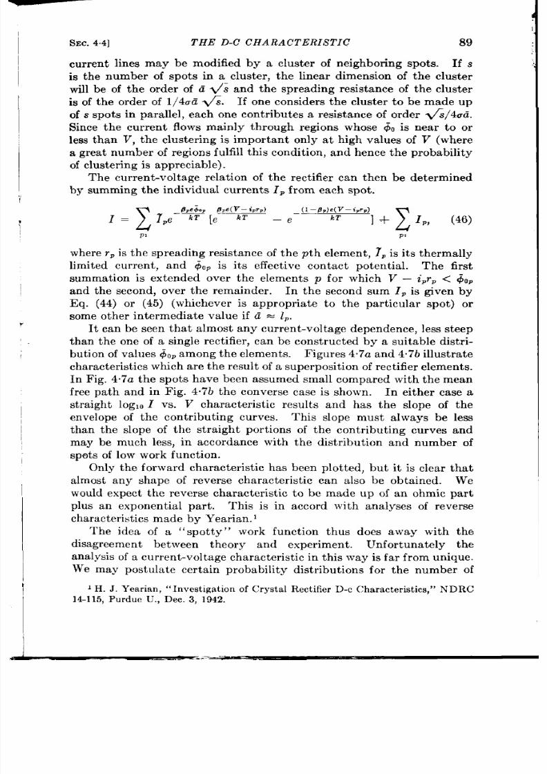
SEC.
4.4]
current
THE D-C
lines may be modified
CHARACTERISTIC
89
by a cluster of neighbor ing spots. If s
I
is the number of spots in a cluster , the linear dimension of the cluster
will be of the orde~ of t i ~; and the spreading resistance of the cluster
is of the order of l/4ud W.
If one considers the cluster to be made up
of s spots in parallel, each on e contr ibutes a resistance of or der {s/4ud.
Since t e cu rrent flows mainly through regions whose & is near to or
less t ha n V, the cluster ing is important only at high values of V (where
a gr ea t n umber of r egion s fu lfill t his con dit ion , a nd h en ce t he pr oba bilit y
of clust er ing is appreciable).
The current -voltage rela t ion of the rect ifier can then be determin ed
by summing the individual cu r rents 1, from each spot .
x
_O*p
PPe(V– i.,.)
(1–8P)e(V–iprr)
I=
~p e kT [e kT – ~- kT
z
1 =1- 1,, (M)
VI
P,
wh er e r = is t he sprea di~g r esist an ce of t he pt h elemen t, 1P is its t herma lly
limited current , and &P is its effect ive contact potent ia l. The fir st
sum ation is extended over the elements p for which V — iprp < &p
and the second, over the remainder . In the second sum 1, is given by
Eq. (44) or (45) (whichever is appropr a te to the part icu lar spot ) or
some other in termedia te va lue if d = l=.
,
It can be seen that a lmost any curren t-voltage depen dence, less steep
than the one of a single r ct ifier , can be const ructed by a suitable dist r i-
(
but ion of va lu es &p amon g t he elemen ts.
Figures 47a and 4.7b illustrate
ch ar act er ist ics wh ich a re t he r esu lt of a super posit ion of r ect ifier elemen ts.
In F ig.
4.7a
the spots have been assumed small compared with the mean
free path and in Fig. 4“7b the converse case is shown. In either case a
straight log,. 1 vs.
V
character ist ic result s and has the slope of the
envelope of the contr ibut ing curves.
This slope must a lways be less
than the slope of the straight por t ions of the contr ibut ing curves and
may be much less, in accordance with the distr ibut ion and number of
spot s of low wor k fu nct ion .
Only the forward character ist ic has been plot ted, but it is clear tha t
a lmost any shape of reverse character ist ic can also be obta ined. We
would expect the reverse character ist ic to be made up of an ohmic par t
plus an exponent ia l par t . This is in accord with analyses of rever se
ch ar act er ist ics made by Yea ria n. 1
The idea of a “ spot ty”
work funct ion thus does away with the
disagreement between theory and exper iment . Unfor tunately the
a na lysis of a cu rr en t-volt age ch ar act er ist ic in t his wa y is fa r fr om uniqu e.
We may postu late cer ta in probability distr ibut ions for the number of
1H. J . Year ian ,
“ Investigationof Crystal Rectifier D-c Characteristics, NDRC
14-115,Pur dueU., Dec. 3, 1942.
90
THE S EM CONDUCTOR—METAL CONTACT IsEC. 45
spot s with given contact potent ia ls @iJ k a nd for @OPit self, a nd pr oceed
to apply them to exper imenta l character ist ics. Although such analyses
have been made, they are somewhat academic because of lack of unique-
ness. The idea of dist r ibuted contact potent ials has been of value, how-
ever , in r econ cilin g t he t heor y of t he d-c ch ar act er ist ic wit h obser va tion s.
It will be fou nd in Ch ap, 6 t o be u sefu l in t he discu ssion of n oise gen er at ion
by cryst a l r ect ifier s.
(#
otalcurrent,——
slope. &
Voltage_
(a) d<< 2
/
/
- Totalcurrent,
slope<*
Ilil
— slope = *
Voltege_
(b) d >>1
F1~. 4.7.—Cur r en t -volt a ge cu rves of two typ ica l r ect ifier s wit h dkt r ibu t ed con t act
pot en tia ls, sh owin g h ow t he t ot al cu rr en t is t he sum of t he cu rr en t con tr ibu tion s (ligh t
lines) from individual epots of d iffe ren t contact potent ia ls .
4.5. Deplet ion Layers.—Up to this po nt we have confined our a t t en-
t ion to the case of a natural bar r ier which by defin it ion consists of the
same mater ial as the bulk semiconductor , with the same density of
impur it ies. Ther e is, however , some reason for believing that t he impur-
ity concent ra t ion in the bar r ier may be lower than in the bulk semi-
con du ct or for silicon as pr ocessed by moder n m et hods for u se in r ect ifier s.
Direct exper imenta l evidence for such a “ deplet ion layer” is scanty.
Its pr esen ce has been in fer red, h owever , fr om t he followin g a rgumen ts.
The theory of high-frequency rect ifica t ion (Sec. 4.6) shows that
r ect ifica t ion (a nd hence conver sion ) efficien cy is a funct ion of t h e quan tit y
w-C, wher e r is the spreading resist ance of the semiconductor and C is the
bar r ier capacitance. The smaller WC is, the grea ter is rect ifica t ion
efficiency. For a natura l barr ier , this quant ity decreases as the number

SEC.
4.5]
DEPLETION LAYERS
91
fVof impur ity levels per unit volume increases. We cannot increase N
indefin itely, however , because the barr ier th ickness is propor t ional to
N-~~ and a poin t is reached at ~vhich rect ifica t ion is limited by leakage
in the blocking direct ion as a result of image forces and tunnel effects.
The obvious escape from this dilem a is to have an ar t ificia l blocking
layer , the th ickness of which depends only weakly (or not a t a ll) on N;
N can then be made large, and r consequent ly small, without the ba rr ier
th ickness being affected and, hence, without C being increased and the
inver se res is tance decreased .
It is well known that rect ifica ion by a silicon-metal contact can be
grea t ly improved (for the same con tact areas), especia lly a t h igh fre-
que cies, by a process of hea t t rea tmen t of the silicon wafer before
assembly. A process of this type was fir st used by the Genera l E lect r ic
Company, Ltd. of England in the manufacture of the Brit ish “red
dot” t ryst al. It is now universa lly used in mo ified form by manu-
factu rers in th e United Sta tes.
This process is fu lly descr ibed in Chap.
10, so it will suffice here to remar tha t it consists essent ia lly of hea t ing
polished silicon wafers in an atmosphere of a ir at a tempera tu re in
the neighborhood of 1000”C for about 1 hr . These wafers are previously
cu t from an ingot of “doped” silicon (tha t is, pu re silicon plus added
impu rit ies or “doping agen ts”).
There is good evidence (reviewed below) tha t the beneficia l effects
of hea t t rea tment a re ascribable to the format ion of a thin surface layer
on t he silicon wa fer , wh ich differ s in it s elect rica l pr oper ties fr om t he bu lk
materia l. In par t icu lar , it is found that much larger inverse resistances
result from contact with the heat -t rea ted su rface than with the or igina l
surface.
It might be con jectu red tha t a layer of differen t materia l (such
as quar z) is formed as a result of the heat t rea tmen t .
As a mat ter of
fact , an oxide surface is cer ta in ly formed by heat ing in a ir . However ,
this is alwa ys dissolved in dilu te h ydr oflu or ic a cid befor e u se of t he wa fer .
Fur thermore, Fox and Pearsa lll have shown that the same beneficia l
effects resu lt from heating in helium or in n it rogen , which are iner t with
respect to the silicon . Fina lly, elect r n-diffract ion studies by Lark-
Horovitzz have revea led no observable difference in crysta l st ructu re
between the prehea t -t rea ted and posthea t -t rea ted (and d oxidized)
sur fa ce. The chara cter ist ic diffra ct ion spots of silicon are fou nd in both
cases.
The conclusion appears inescapable tha t a thin layer is formed on the
he&trea ted surfa e and tha t th is layer differs on ly in impurity con ten t
1M.
Fox and C. S. Pearsal l,“Results of Heat-t reat ingSilicon in Various Atmos-
pheres” (Colloquium on Crystal Rectifiers,Vacuum Tube Developmen t Committee),
NewYork, Mar . 27 , 1944.
3Privatecommunication.
92
THE SEMICONDUCTOR-METAL CONTACT
from the in ter ior . The theoret ica l arguments above then
th is is a deplet ion layer .
[SEC. 45
indicate that
For the- sake of ‘clar ity the case for a deplet ion layer has perhaps
been somewha t over simplified .
Besides (and previous to) hea t t rea t -
ment the surface of the silicon afers are a lways highly polished to a
mir rorlike finish . It has been on jectured tha t this polish lng produces a
flow layer which independen tly modifies th e elect r ica l proper t ies of th e
surface. High in verse resistance is n ot obta ined by th e polish ing act io ,
however , and is produced only by the sub equent hea t t rea tment .
According to the exper ience of the Bell Telephone Labora toriesjl the
results of the hea t t rea tment do not depend on the texture of the surface.
The funct ion of the smooth surface, these invest iga tors believe, is to
facilita te tapping and r educe the noise outpu t of the rect ifier .
It has already be n men tioned tha t hea t t rea tmen t result s in an
in crease of resistance in t he blocking direct ion .
That this effect is a
proper ty of a sur face layer may be demonst ra ted by etchings the surface
elect rolyt ica lly in 24 per cent HF.
As t he et ch in g pr oceeds, t he in verse
resist an ce of t he silicon decr ea ses u ntil it even tu ally r ea ch es a nd r ema in s
at its va lu before the heat t rea tment .
Th e effect of h ea t t rea tm en t is a som ewh at cr it ica l fu nct ion of t emper -
ature.
Fur thermore, increasing the t ime of heat rea tment apparent ly
produces a result similar to that obta ined by raising the temp ra ture.
Some data bear ing on these effects are given in Sec. (10.4). Fur ther
evidence of the format ion of a thin surface layer of specia l proper t ies is
found by heat -t rea t ing, gr inding or etching off the surface, a d heat -
t rea t ing again a t a different tempera tu re. The proper t ies of the wafer
then correspond to the final, and not to the init ia l, tempera ture.
It has been ment ioned tha t the heat t rea tment improves high-
fr equ en cy per forma nce (r ect ifica tion a nd con ver sion efficien cy) for t he
same con tact area . Now con tact areas of rect ifiers using natura l silicon
(no heat t rea tment ) must be mad very small for good microwave per-
f ormance. Such rect ifiers tend to be mechanically and elect r ica lly
unstable and are especia lly uscept ible to burnout by leakage power
through the TR switch , as well as by accidenta l exposures to elect r ica l
power.
The grea t benefit of the heat -t rea tment process has accrue
from the large contact areas it has made possible and the consequen t
mechanical and elect r ica l stability with no impairment , in fact , with
consider ab e improvemen t , in conver sion efficiency.
It is probably safe
1see W. G. Pfann, “Oxidat ion f Silicon for Point -cont actRectifiers,))BTL RePOrt
MM-4> 1201OO,Sept. 22, 1943,for a good account of the experimentaleffectsof heat
treatment .
2This processactually removesa layer of silicon from the surfaceand is not to be
confused with the p revious ly men t ioned remova l ~ f the oxide layer by d ilu t e HF
(nonelectrolytic).
1
I

.
SEC. 4.5]
DEPLETION LAYERS
93
to say that no innolra t ion in crysta l manufactur ing techn ique has con-
t r ibuted so much to impro~ed crysta l per formance as has the heat -
t r ea tmen t p roces s.
Difusion and Evaporatio of Im purities as lleans jor the Productio~l
of a Depletion Layer.—It was suggested by Bethe] tha t a deplet ion layer
might be formed by passing a la rge cur ren t th rough a crysta l rect ifier in
the forward direct ion , the supposit ion being tha t the la rge cur ren t
wou ld ra ise th e t em per atu re of t he con ta ct h igh en ough t o ca u e diffusion
of im pu rit ies in t he ba rr ier la yer .
At the sa e t ime, th direct ion of the
a pplied volt age is su ch t ha t it will a cceler at e pos t ively ch ar ged don at or s
(n -type semiconductor ) or nega t ively charged acceptor s (p-type semi-
conductor ) in to the in ter or of the semiconductor and will therefore
)
deplet e the su rface layer of cha rged impur it ies. This suggest ion was
made to expla in the observa t ion of Lawson and co orker s tha large
forward curren t s have the effect3 of increasing the rever se resistance at
1 volt .
The suggest ion tha t hea t t rea tmen t of a silicon wafer produces a
deplet ion layer by a process of diffusion and evapora t ion of impur it ies
was made by Ser in and Stephens,4 who gave a mathemat ica l t rea tmen t
of t he dif usion and eva pora tion pr ocess which is r epr odu ced h er e in pa rt .
F
Consider a semi-in fin ite homogeneous block of semiconductor with a
plane face at z = O and extending in the posit ive z-direct ion . Suppose
tha t a t t ime t = O t he block has a un iform concen t ra t ion NO of impur ity
atoms.
The concen t ra t ion N(z,t ) a t a distance z from the surface a t
som e la ter t im e
t
is given by the solu t ion of the diffusion equat ion ,
(47)
tha t sa t isfies appropr ia te boundary condit ions. Here D is the diffusion
coefficien t , a ssumed indep enden t of t h e con cen t ra t ion .
The ra te of loss of impur ty atoms per unit a rea from the sur face is
assumed to be propor t iona l to the sur face concen t ra t ion . This ra te of
loss must equal the ra te of ar r iva l a t the su rface by diffusion , if there is
to be no piling up of impur ity a toms on the surface. Thus, one boundary
condit ion is
—
#+hN=O
atx=o,
(48)
1H . A. Bet he, ‘( Th eor y of H igh -fr equ en cy Rect ifica tion by Silicon Crysta ls,”
RL Repor t No. 4%11, Oct . 29, 1942.
z A. W. La wson et a .,
“D-c Bu rn -ou t Temper at ur e in Silicon Rect ifier s, ” h ’DRC
14-113, Univ. of P en n., h ’ov. 1, 1942,
t Th ese exper imen ts wer e per formed on silicon t ha t h a d not been h ea t -t rea t ed.
?
4 B. Ser in and W. E. Stephens, “ P roduct ion and Effects of a Deplet ion Layer in
Doped Siiicon ,” NDRC 14282, Univ. of Penn., May 29, 1944. See a lso, B. Ser in ,
Phys . Rev., 69, 357 (1946).
94
THE S EMICONDUCTOR—METAL CONTACT
[SEC.45
where
h=:!
(49)
and K is the ra t io of the ra te of loss per unit a rea by evapora t ion to the
surface concent ra t ion . The other boundary condit ions a re
N(z,o) = No forx >0,
N(u J ,t ) =N,.
I
(50)
The problem is formally equivalent to an analogous solved problemL in
heat flow, namely that of a semi-infin ite body in it ia lly a t a uniform
tempera tu re losing heat by radia t ion in to a region at zero tempera tu re.
Thus the solu t ion may be writ ten down at once as
: = e r f ( a + e h + h ’ ” t [ ’erf(i$%+h=w51)
where
Of especia l in terest is the solu t ion after sufficien t t ime has passed
with the result N(O,t)/NiI = CM<< 1.
Under t h is condit ion ,
(53)
and the solu t ion ~q. (51)] reduces approximately to
F igure 4.8 shows a plot of N/No as a funct ion of x in units of
d G
I/haO.
r
In plot t ing this curve it has been assumed that a, = 0.1.
The diffusion coefficien t may be expressed in terms of a tomic param-
(
eter s by
D = abze ~T,
(55)
where a is the “jumping” frequency of a subst itu ted impurity a tom in
the bulk crysta l la t t ice, 6 is the distance between adjacent bulk atoms,
cD k th e diffusion act iva t ion energy, k is Boltzmann’s constant , and T is
t h e a bsolu te t emper at u re.
1See H. S. Carelaw,I t ircducLionto theMathem atical The~ of tlw Conduction of
~
Heal in S old , 2d
cd.,
Macm illa n, Lon don , 1921, &c. 25.
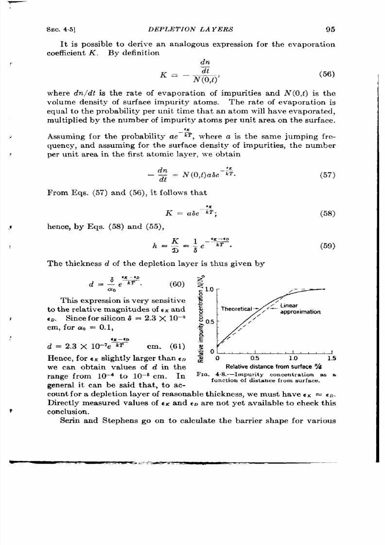
SEC. 4.5]
DEPLET ION LAYERS
95
It is possible to der ive an analogous expression for the evapora t ion
coefficien t K. By defin it ion
(
dn
z
K = – N(o,t )’
(56)
where dn/ d t is t he ra te of evapora t ion of impur it ies and N (O,t ) is the
volume density of su face impur ity a toms.
The ra te o evapora t on is
equal to the probability per unit t ime tha t an a tom will have evapora ted,
mult iplied by the number of impurity a toms per unit a rea on the surface.
Assumin g for t he pr oba bility ae
‘~T , ~},here a is the same jumping fr e-
quency, and assuming for the sur face density of impur it ies, the number
,
per unit a r ea in the fir st a tomic layer , we obta in
dn
——.
dt
N (O,t)abe V.
(57)
From Eqs. (57) and (56), it follows tha t
K = a~e ~T;
(58)
,r
hence, by Eqs. (58) and (55),
h=~=~e–~
~
Da ”
(59)
The th icknes s d of the deplet ion layer is thus given by
d = ~ e’=ki’”. (60) ~l,o
~o
E
/- -
This expression is very sensit ive ~
/
Z’ Linear
t o the reia t ive magnitudes of c. and ~
Theoretical- , /— ~pproXimation
r
cD. Since for silicon = 2.3 X 10 8 5 ~5 ,z’
cm, for aO = 0.1,
,=
/
~
/’
/
t=—.ll
d = 2.3 X 10_7e ‘T
cm. (61) ~ ~ “
H en ce, for cx sligh tly la rger t ha n CD ~ O
0.5
1.0
1.5
we can obtain
va lues of d in the
Relativedistance from surface ~d
range fr m 10–8 to 10–6 cm. In
F IG. 4.&-Impu rit y con cen t ra t ion a s a
fun ctionof dista ncefrom su rface.
genera l it can be sa id tha t , to ac-
coun t for a deplet ion layer of reasonable th ickness, we must have c~ =
eD.
Direct ly measured va lues of cii and m are not yet available to heck th is
*
conclusion.
Ser in and Stephens go on to calcu la te the ba rr ier shape for var ious
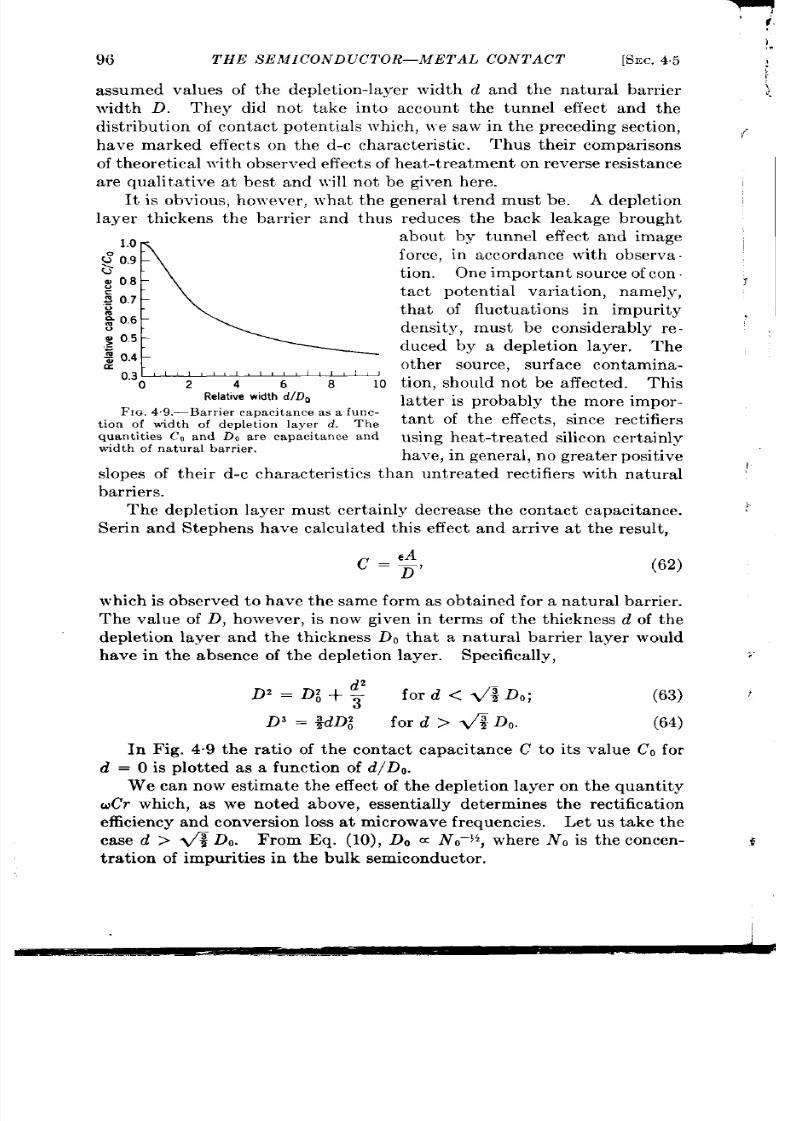
,“
r.
96
THE SEMICONDUCTOR—METAL CONTACT
[SEC.45
assumed va lues of the deplet ion -layer width d and the nat ra l bar r ier
width D. They did not t ake in to account the tunnel effect and the
dist ribu tion of con ta ct pot en tia ls ~vh ich , \ vesa \ v in th e pr ecedin g sect ion ,
h ave ma rked effect s on t he d-c cha ra ct er ist ic.
Th us t heir compa rison s
of t heor et ica l wit h obser ved effect s of h ea t-t rea tm en t on r ever se r esist an ce
a re qualita t ive a t best and will not be given here.
It is obvious, however , wha t the genera l t r end must be. A deplet ion
layer th ickens the ba r r ier and thus educes the back leakage brough t
1.0
L
about by tun el effect and image
G 0,9
for ce, in a ccorda nce with obser va .
b
t ion . Oneimpor tan t sou rce of con .
~ 08
tact poten t ia l var ia t ion , namely,
5 0.7
:
that of fluctua t ions in impur ity
: 0.6
“
density, must be considerab y re -
$J0.5
duced by a deplet ion layer . The
g
g
0.4
other source,
su rface con tamin a-
0.3
0
2
4 6
8
10 t ion , should not be affect ed. This
Relative
widthd/D.
la t ter is probably the more impor-
FIG,4.9,—Bar r iercapacita nceas a func-
t ion of width of deplet ion layer d. Th e
tan t of the effect s, since rect ifier s
qu an tit ies (’n a nd Do a re ca pa cit an ce a nd
u sin g h ea t-t rea ted silicon cer ta in ly
wid th of n a tu r al ba r rier .
h ave, in gen er al, n o gr ea ter posit ive
slopes of their d-c cha ract er ist ics than un t rea t ed rect ifier s with na tu ra l
barriers.
Th e deplet ion layer must cer ta in ly decr ea se t he con tact ca pacit an ce.
Ser in and Stephens have ca lcu la ted th is effect and a r r ive a t the resu lt ,
(62)
which is observed to have the same form as obta ined for a na tura l ba r r ier .
The value of D, however , is now given in terms of the th ickness d of the
deplet ion layer and t he th ickness Do tha t a na tu ra l ba r r ier layer wou ld
have in the absence of the deplet ion layer . Specifica lly,
D,=+
ford < 4%Do;
(63)
D3 = ~dD
for d > m Do.
(64)
In Fig. 4.9 the ra t io of th con tact capacit ance C to its va lue C, for
d = O is plot t ed as a funct ion of d / Do.
We can now est ima te the effect of the deplet ion layer on the quant ity
d7r which , as we noted above, essen t ia lly det ermines the rect ifica t ion
efficien cy and conver sion loss a t m icr owave fr equ en cies.
Let us t ake the
case d > ~ Do.
From Eq. (10), DO cc N O–J ’J , where No is the concen- $
t ra tion of im pu rit ies in t he bu lk sem icon du ct or .

SEC. 46]
RECTIFICATION A T HIGH FREQUENCIES
97
The spreading resistance r is by 13q. (34) inversely proport ional to
O, the conduct iv ty y, and consequent ly is by Eq. (19) inversely pro-
port ional to n, the bulk elect ron density, which in turn depends on No,
the impurity concent ra t ion . If the ioniza t ion of impurit ies is near ly
complete in the bulk semiconductor , as in germanium (Sec. 3.5), n = No.
For the other ext reme of weak ionizat ion n c NW, see Eq. (5). The
ca se of silicon n orma lly fa lls somewh er e between t hese ext remes.
Thus
we h ave t he followin g depen den ce of D and uCr on No:
1. With n o deplet ion layer (na tura l ba rr ier ),
D = DO m NO–~~,
&’r cc NO–~~ (complete ionization), wCr does n ot depen d on
}
(65)
NO (weak ioniza t ion).
2. Wit h a deplet ion la yer of t hickn ess D > 4$ Do, D E NO–~i,
UC’T a N O–~~
(complete ioniza t ion), t iCr a NO–)6 (\ veak
)
(66)
ionization).
Thus the effect of the deplet ion layer , as expected, is to increase t e
dependenc of uCr on NO and to decrease the dependence of the barr ier
thickness
Don
N,. The deplet ion layer thus makes it possible t o improve
r ect ifica tion b a decr ea se in aCr con sequ en t t o an in cr ease in NOwith ou t
a ser iou s r edu ct ion in ba rr ier t hickn ess.
4.6. Rect ifica t ion at High Frequencies. Genera l Considerations.—we
have seen (Sec. 2.4) tha t a crysta l rect ifier can be represented approxi-
mately by” the equivalent circu it of
Fig. 4.10. The barr ier resistance R,
which depends on the voltage across
it , is shunted by the barr ier capaci-
tance C, and this combinat ion is in
ser ies wit h t he ohmic spr ea din g r esist -
ance r of the bulk semiconductor . At
low frequencies, wCR <<1 even wh er e
R is t he maximum ba rr ier r esista nce;
-lCd
FIG, 4.10.—Equ iva len t cir cu it of a
crys t al r ect ifier ; R is the non linear
ba r rier , C’ t be ba r rier capa cit a nce, a nd
r tbe ohmic spread ing res is t ance.
the capacitance can then be completely ignored and the rect ifica t ion is
det ermin ed en tir ely by t he d-c ch ar act er ist ic.
At m icr owa ve fr equ en cies, h owever ,
the capacit ive susceptance UC
of the barr ier is actually large compared with 1/R in t he ba ck dir ect ion
and consid rable modificat ion of the rect ifying proper t ies should be
expected. Measured barr ier capacitances range from 0.02 to 1.0 ppf,
the smaller values being found in crysta ls prepared for use in the l-cm
band and the larger va lues in high-burnout , 10-cm band rect ifiers. A
capacitance of 1 ppf has a reactance of only 50 ohms at a wavelength of
10 cm; whereas back resistances normally encountered are 5000 ohms
~
or more. Thus the back resistance is effect ively shunted by the barr ier
ca pa cit an ce at micr owa ve frequ en cies and may t her efor e be ign or ed.

98
THE S EMICONDUCTOR—METAL CONTACT
[SEC.4.6
The rect ifica t ion efficiency and ther efore a lso the conver sion loss
sh ou ld depen d on t he r at io of ba ck -t o-forwa rd impeda nce.
At reasonably
R
t he ba r r ier r eact ance l/uC and with the spreading resist ance r . The
forward resistance is then just r .
For any back volt age and for reason-
a bly small forwa rd volt ages, R is very la rge; ther efore the impedance of
the con tact proper is ju st –j/wC and the tot a l back impedance is
Z=r –-.$.
(67)
The “ back-to-fron t” ra t io is
z
=1–J.
7
UC?-
(68)
Dimensiona l considera t ions a lone make it clea r tha t r ect ifica t ion
efficien cy a nd con ver sion loss, bot h dim en sion less qu an tit ies, ca n depen d
on the crysta l pa rameters on ly through the factor &r .
Clea rly, t he
ba r r ier r esistance is a lways negligible; it is eit her shunted by the bar r ier
capacitance or is small compared with the spreading resistance.
Only
over a small r an ge of for wa rd volta ge does it cont ribu te t o th e impeda nce.
Th e con ver sion loss L is thus a funct ion of d7r , obviously an increas-
ing funct ion , and low conver sion lo s requir es a small va lue of d%,
cer t a in ly less than unity. We can express uCr in terms of the proper t ies
of the semiconductor by use of Eqs. (34) and (17). We obta in
(69)
where the radius of the con tact a , t he ba r r ier th ickness D, and the wave-
length X are in cen t imeters; and the conduct ivity u is in mho-cm-’. If
for example, i = 3 cm, D = 2 X 10-g cm, c = 13c0, and u = 50 mho/cm,
then uCr will be less than unity, provided
(70)
Contacts actua lly used fu lfill th is condit ion by a wide margin . A
represen ta t ive va lue of a for 3-cm-band crysta l con tact s is 3 X 10⁻⁴ cm.
Wit h t he a bove va lu es of c/cO an d D, su ch a con ta ct wi l h ave a ca pa cit an ce
of 0.1 ppf and the spreading resistance will be 17 ohms.
To improve rect ifica t ion we need to make the quant ity ea /.Di as
small as possible. An obvious solu t ion is to decrease a . the con tact
radius. Unfor tuna tely very small va lues of a lead to mechanica l and
elect r ica l instability. Bethel has suggest ed a way ou t of th is dilemma
‘ H. A. Bet he, “Th eor y of H igh Fr equ en cy Rect ificat ion by Silicon Cr yst als,”
RL Repor t No. 43-11, Oct . 29, 1942.
.

SEC. 4.6]
RECTIFIC TION AT HIGH FREQUENCIES 99
by using an elonga ted, or kn ife-edge, con tact . It can be shown tha t the
pa rameter a in Eq. (69) is then replaced (approximately) by the shor t
dimension of the con tact . Thus a con tact of fa ir ly large area , and hence
..
good tability, can be obta ned with no sacr ifice in conversion loss. This
poin t is discussed more fully in Chap. 8. It was a t one t ime believed
that the excellen t performance of t e Br it ish “ red dot” crysta ls was
essent ia lly a ch ieved by making th ese crysta ls with an elon gat ed con tact .
This view is no longer hel , however .
It may be shown theoret ica lly
tha t very la rge ra t ios of long-to-shor t dimensions of the contact must
obta in before the beneficia l effects become impor tan t and the actual
dimensions of the “red dot” con tact s do not appear to meet th is ext reme
,
condit ion . Fur thermore, exper imen ts by Fox and Pearsa ll and by
St eph en s’ h ave sh own n o sign ifica nt differ en ce between kn ife-edge con -
tacts of the ‘(red dot” type and circu lar contacts, either with respect to
conversion loss or stability. At tempts have been made to increase the
ra t io of long-to-shor t con tact dime sions to a va lue tha t wou ld be
expected to improve per formance, but the techniques for making such a
con tact a re ext remely difficu lt and no success has as yet been at ta ined.
A se ond escape from the dilemma is to increase the parameter
D
the
t hick ness of t he ba rr ier la yer .
As we have seen in the preceding sect ion ,
th ere is good reason to believe that th is is actua lly acc mplished by hea t -
.;
t r ea tmen t of the silicon wafer s, follo~ving the ‘[ r ed dot” techn iques or a
modifica t ion of them. The rea l va lue of th is format ion of a deplet ion
layer is a consequence of the fact tha t it makes possible an increase in
t he va lue of a by an in cr ea se in t he impur ity con ten t of t he sem icon du ctor
withou t a simultaneous decrease in D. This poin t will not be fu r ther
t r ea ted h ere, since it wa s discu ssed in deta il in th e pr ecedin g sect ion .
An increase in u without an effect on the other pa rameters migh t be
at ta ined by an increase in ca r r ier mobility Eq. (3”21). Thus germanium
is known (Sec. 3.7) to have about th ree t imes the mobility of silicon .
Other th ings equal, german ium should h erefore be puper ior to silicon .
It is found, however , tha t germanium does not yield to heat -t rea tment
in the same manner as ilicon , and ermanium rect ifiers tend to be some-
wh at “ n oisier ” t ha n silicon r ect ifier s.
Weldin g of a small met al-sem icon du ct or con ta ct impr oves mech an ica l
st abilit y enormou sly and ma + a lso improve elect rica l st abilit y (r esist a nce
to burnou t ). No one has yet succeeded in welding meta l wires to silicon .
Welded meta l-germanium contacts a re discussed in Chap. 13. They
ha ve such specia l and peculia r pr oper t ies tha t th ey can not be adequa tely
1SeeM. Fox,
“Com par ison of Con e and Wedge Tips on Radia tion Labor atory
Silicon ;“ a nd W. E . Steph en s,
‘‘ Com pa rison of Con e a nd Wedge Tips on Ra dia tion
<
Labor atory Silicon” (Crysta l Rect ifier Conference, Va cuum Tube Developm ent
Commit tee), Nov. 19, 1943.
i
100
THE S EMICONDUCTOR—METAL CONTACT
[SEC.d 6
t rea ted by the simple considera t ions above. It is r emarked here on ly
tha t they have not a yet bee brough t to the poin t where they can replace
s ilicon r ect ifier s t o advan t age.
Theon ly oth er pa rameter isc/cO, the dielect r ic constan t . As poin ted
ou t in Sec. 4.2, a h igh dielect r ic const an t is necessa ry for the format ion
of a na tura l ba r r ier . The use of an ar t ificia l ba r r ier layer lessens the
impor t ance o a high dielect ric const an t.
Perhaps someth ing migh t be
ga ine by using a semiconducto tha t has a lower dielect r ic const an t and
a n a rt ificia l ba rr ier la yer .
Relaxation Effect s. -Lawson and ot her sl h ave n ot ed tha t th e r ect ifica-
t ion efficiency of cryst a l r ect ifier s does not decrease with fr equency as .
rapi ly as migh t be expected from the observed va lues of ba r r ier capaci-
tance and d-c cha ract er ist ic. It is obvi usly impor t an t to understand
the na tu re of th is effect . Once it s cause is made clea r , some means may
be fou nd t o en ha nce it and t hereby increa se t he u tility of cr ysta l r ect ifier s
a t h igh frequencies. Lawson ascr ibes the effect t o relaxa t ion processes
in the bar r ier layer . It is reasonable, bu t not cer t a in , tha t Lawson’s
explana t ion is cor rect . This sect ion is devoted to an exposit ion , in
modified for m, of h is t heor y. 2
We have seen tha t the capacitance of the bar r ier is caused by the
flow of elect rons in to and ou t of the ba r r ier layer . The cha rging cur ren t ,
is in quadra tu re with the applied volt age and the ba r r ier layer thus act s
as a c ndenser . In the ana lysis of the capacitance given here, it has so
far been assumed tha t the elect rons r main permanen t ly “fr ee,” and can
therefor e respond withou t t ime lag to a sudden change in voltage. The
possibility should now be considered tha t some of the elect rons may
become t rapped by combina t ion with cha rged impur ity a toms. The
elect rons in the ba r r ier will eit her be fr ee or bound to impur ity a toms.
Let us fir st consider the ca e for wh ich the frequency j is small compared
with the probability B per unit t ime for ioniza t ion of an impur ity a tom.
The fr ee elect rons will emerge from the ba r r ier as soon as their poten t ia l
energy exceeds the potent ia l energy of an elect ron in the bulk semicon-
ductor . The bound elect rons will emerge somewha t la t er , bu t , if B >> j
as assumed, their t ime lag will be small compared with the ha lf per iod of
the wave and they con t r ibu te equally to the quadra ture componen t of
t he cu rr en t.
If, however , ~
= 1?, the t ime lag of the bound elect rons will be an
a ppr ecia ble pa rt of a h alf cycle.
Th e cu rr en t pr odu ced by t he emer gen ce
of the bound elect rons will then consist of two componen ts, one in phase
1See A. W, Lawson , et al.,
‘(H igh -fr equency Rect ifica t ion Efficiency of Crys ta ls , ”
NDRC 14-153, Un iv. of P en n,, J u ly 1, 1943; a nd l’;. It . Ber in ger , “Cr yst al Det ect or s
a n d t h e Cr yst al Vid eo Receiver , ”
RL Repor t No. 638, Nov. 16, 1944.
z A. W. Lawson, et al.,
“ Ion iza t ion of Donat or Levels in Crystal Rect ifier s by
I
Th erma l Agit at ion ,” NDRC 14-173, Un iv. of P en n., J ,]ly 7, 1943.
.,
}
?-
SEC. 46]
RECTIFICATION AT HIGH FREQUENCIES 101
b
an d on e in qu adra tur e with th e volt age.
Sin ce t he t ot al ch ar gin g cu rr en t
(quadra tu re componen t ) is now reduced, it is clear ‘tha t the effect ive
ba rr ier capacitance is less than at low frequencies (f<< 1?). Fur ther -
more, there will now be a conductance G shunt ing he barr ier , because
of the in-phase componen t of the curren t .
At st ill h igh er fr equ en cies, j >> B, an elect ron that had become bound
dur ing the discharging par t of a cycle may wait for severa l cycles before
again con tr ibut ing to the cur ren t . The charging cu rren t (and therefore
the bar r ier capacitance) is thus st ill fu r ther reduced. The in-phnse
cur ren t , and thus the conductance G, shou ld increase with frequency in
th is region , approach ing a constant va lue in the limit , since the ra te of
ioniza t ion of donators would be nea r ly constan t dur ing a half cycle a t
ver y high fr equen cies (j>> B).
The magnitude of these effe t s clear ly depends on the ra t io of free-
t o-bou nd elect r n s a t equ ilibr ium.
If th is ra t io is la rge, the relaxat ion
effect s will be r ela t ively un impor ta nt .
If the ra t io is small, the impor-
tance of the effect s a t microwave frequencies depends on the magn itude
of B. We have seen in Chap. 3 tha t ioniza t ion of impur it ies is 20 to
40 per cen t complete in the case of silicon and near ly 100 per cen t com-
plete for german ium at thermal equilibr ium (room tempera tu re) in the
bulk semiconductor . Thus if the su rface levels a re of the same character
in the bulk impur ity levels, we should expect no relaxat io effects in
germanium rect ifier s bu t possible relaxat ion (depending on the value of
B) in silicon rect ifiers. It is possible, h owever , tha t sur face levels exist
which a re of an ent irely differen t na ture from the bulk impur ity levels.
Any in ter rupt ion in the per iodic st ructu re of the la t t ice, such as tha t
occurr ing a t the su rface, is capable of producing elect ron evels in the
normally forbidden region of the band st ructu ra (Sec. 3.1). These
surface levels mig t lie a t much grea ter depths below the conduct ion
band than the impur ity levels. 2
If th is is the case, we should expect
st ron g r ela xa tion effect s in bot h silicon a nd germa nium.
The magnitude of the relaxat ion t ime l/B is of grea t impor tance in
th e t heor y of th e relaxat ion effect s.
The value of B may be est im ated’
a s follows: Th e equ ilibr ium of t he r ea ct ion ,
F ree elect ron + bound hole & bound elect ron ,
1F . Seit z, The Modern Theory of Solids, McGr aw-H ill, N ew Yor k, 1940, pp. 320 ff.
I S om e eviden ce t ha t t his is t he ca se for silicon is obt ain ed fr om stu dies of ph ot o-
conduct ivity h y Miller (P . H. Miller and hi. H. Greenbla t t , “ Photoeff ects in Pure
Silicon ,” NDRC 14-412, U niv. of P en n., Ma r. 20, 1945), wh o fou nd t ha t t he t hr csh o,d
for photoconduct ivity in silicon is shout 0.5 cv; whereas the band separa t ion in
silicon is known to be 1.1 volts (Sec. 35). His resu lt s might be expla ined by the
h ypot hesis of su rfa ce levels lyin g 0 5 volt below t he condu ct ion ba n d.
3N. F. Mott and R. W. Gurney, Electronic Process in Ionic Crystals, Oxford,
New York 1940, p. 108.
..
-
E.G. & G. LIBRARY .: -“’‘~ ‘,. .,,. ,.
LAS VEGAS- BRANCH
‘..,
I
102
THE S EMZ ONDUCTOR—METAL CON TACT [SEC.4.6
is governed by the mass act ion law,
~2
()
2wnlcT ‘e-~
IV-n=2 h’
s
(71)
where
n = number density of fr ee elect rons,
N = number density of impur ity levels,
AE = depth of an impur ity level below the conduct ion band.
The r ight -hand member of Eq. (71) is the equilibr ium constant of the
r ea ct ion [see Eqs. (3.1) an d (3.2)].
This resu lt determines the number of free elect rons at equilibr ium.
For a nonequilibr ium (and elect r ica lly neut ra l) sta t e, applica t ion of
det ailed ba la ncing gives
dn
z
= B(N – n ) – An’, (72)
where B is t he probability per unit t ime for an elect ron t ransit ion from
the bound to the free sta te and An2 is the number of t ransit ions per unit
t im e in t he opposit e dir ect ion .
Now A may be formally writ t en as
A = uU,
(73)
where u is the captu re cross sect ion of an empty dona tor level and u
is the mean thermal velocity of an elect ron in the free sta t e.
From
Eq. (72) equilibr ium occu rs when
~2
B
N–n=~”
Compar ing this with Eq. (71) and inser t ing Eq. (73), we get
where we have in t roduced for u the expression ,
H “
u = 3kT ‘5
m
(74)
(76)
The quan tit y B may be est imated from Eq. (75) by taking u = 10_16cmz,
whence
B = 1.5 X 101le ‘;
see–l.
(’77)
Th er e is some exper imen ta l evidence that BO, t h e coefficien t of CAElkT
in this expression , ay be as low as 1010see–l. Thk la t t er value is based
on the ra te a t whic elect rons must be freed thermally from t rapping
i

SEC.
4.6]
RECTIFICATION AT HIGH FREQ ENCIES 103
cen ter s in r ock salt in order to expla in the observed tempera tu re depend-
ence of photoconductivity.’
A bet ter est ima te of B may be had by trea t ing the problem wit the
a id of quantum mechanics. In th is way Seitz2 has obta ined 1010 see-l
as an upper limit for BO, and Lawsons concludes tha t BOis abou t 2 X 10g
see–1, if AE < k8D, where 6D k the Deb ye tempera tu re of silicon . If
AE > k@D, he finds that BO may be as small as 106 see–l. Since these
est imates a re of the order of, or smaller than , microwave frequencies, it
is clea r th at a con s der able r ela xa tion effect m ust be a nt icipa ted.
In Lawson’s t r ea tment of relaxa t ion theory the assumpt ion is made
that the t ime for the inverse process, tha t is, elect ron capture by an
ion ized donator , is shor t compared with the microwave per iod.
Th e
t ru th of th is assumpt ion may be invest iga ted by calcula t ing the t ime
for the a t ta inment of equilibr ium, star t ing from an elect r ica lly neu tra l
sem icon du ct or wit h complet ely ion ized don at or s.
The relaxat ion t ime
for th is process is found by in tegra t ing Eq. (72). It is
‘ = (2N : no)ll’
(78)
wh er e n o is th e equilibrium valu e of n .
If B = 10’0 see-’ and n,/N = 0.2
(a typica l va lue for silicon), w’e obta in 7 = 1.1 X 10-” sec which , a lthou gh
less than microwave per iods in use, cannot be rega rded as negligibly
small. 4 Lawson’s resu lt s must th erefore be in terpreted with cau tion ,
a lthough there is no doubt tha t h is theory is qualita t ively correct .
These considera t ions will now be applied to the following problem.
We assume a barr ier layer co ta in ing N impur ity levels per un it volume
loca ted at an energy depth AE below the conduct ion band. In the bulk
sem icon du ct or , t her e a re nOfr ee elect ron s per u nit volume.
Th e ba rr ier
layer is assumed to have, before an a lternat ing voltage is applied, a
u niform spa ce-ch ar ge den sit y eN .
It is assu ed tha t there is an abrupt
t ransit ion from the charged barr ier layer to the neu t ra l bu lk semicon-
ductor . An alterna t ing sinusoida l voltage’ VO cos u t is applied to the
ba rr ier ; t his causes t he potent ia l of the bulk semiconductor to va ry
sinusoidally with the t ime. When the po en t ia l r ises, elect rons flow
1N. F. Mot t and R. W. Gurney, op. ck , p. 136.
9 F. Seitz, “ Tr ansit ion P roba bilit y for E xcita tion fr om Bou nd Levels” (Cr yst al
Rect ifier Con fer en ce), Columbia Univ. Sept . 11, 1943.
j A. W. Lawson et a l., N IYRC Repor t 14-173, Un iv. of P en n., J u ly 7, 1943.
~In the case of sur face levels n~/N might be much small r than 0.2 and hence r
muchsh orter tha n 10–11sec.
s In th is sect ion uoltuge(and the synonymous term poten~ia l)s definedfor con-
venienceas the potential en er gy of an elect r on divided by the a bsolu te va lue of the
elect ronic cha rge, It thus has the opposit e sign of the conven t iona l voltage. This
fact must be bor ne in m in d in in ter pret n g the results.

104 THE S EMICONDUCTOR—METAL CONTACT [SEC.4.6
in to the bar r ier and neutra lize a par t of it s volume.
In a ccor da nce wit h
t he above discussion, t he equilibr ium fr ee-elect ron density is assumed t o
be established immedia tely. When the volt age wave recedes, elect rons
pour out of barr ier . It is assumed, and easily just ified, tha t the free
elect rons will slide down the potent ia l hill in a t ime shor t compared with
the per iod of the wave.
The bound elect rons will leak ou t of the barr ier
at the ra te B(N – n). Once having escaped from the impur ity ions,
these elect rons will a lso be assumed to depar t instantaneously. A small
decr ea se V in potent ia l exposes a fract ion (d j/ dV) AV of the volume j
of the bar r ier t o the elect on-st r ipping process and charges thk par t
of the bar r ier by the amount enO(dj/dV) AV at once and by the amount
I
I
I
%
I
3
I
I
I
1,
0
b It ’
T .t “
T~
t
,,
Time —
I
I
I
I
FIG.4.11.—Ba rr ier volt a ge vs. t ime. Th e t imes t ’ a n d t “ a r e fidu cia l t imes for d own swin g
a nd upswin g r esp ect ively, a n d r is t ime in gen er a l.
eN(df/d V) AV even tu ally, if su fficien t t im e ela pses befor e t he pot en tia l
r ises again for t he don at or s t o become ion ized complet ely.
Figure 411 shows t e form of the volt age wave VO cos & At t = O,
the potent ia l begins to recede. The cur ren t a t t ime O
T is the per iod of the vo tage wave) is in two par ts.
1.
2.
That due to the fr ee elect rons tha t depar t in
t ’ + fit ’.
This cur rent is given by
dj dV
il =
‘en” Tv 77’
d f
—
enovo m u ‘in ‘t’”
< t’ < ~T (where
the in terva l t ’ t o
(79)
The sign has been chosen so that a posit ive cur r en t increases the
posit ive cha rge on t he barr ier .
That due to the evapora t ing bound elect rons. These elect rons
come cont inuously from the par t of the bar r ier exposed dur ing the
interval O t o t ’. If , is some gener ic t ime in this in terval, the
—
SEC. 4.6]
RECTIFICATION AT HIUH FREQ UENG’IES
,,
105
{
!,
cont r ibu t ion from a small in t erva l d7 at 7 is
,’
(80)
In t egra t ing th is from O to t ’, we obta in
df B .
iz=e(N–nJm Vo~
(se-’” + B sin d – o cos d’). (81)
Let us now consider the cu r ren t s flowing in the t ime in terva l
~T < t“ < T .
This cu r ren t is a lso composed of two par t s.
1. The cur ren t flowing in to the volume (d f/ dV) dV flooded by the
advancing wave dur ing the small in t ervaI W’ at t“. The amoun t
of charge in th is pa r t of the ba r r ier is tha t remain ing a ft er remova l
of the fr ee elect rons a t t = T — t“ a nd t he su bsequ en t eva por at ion
from the dona tors du r ing the in t erva l 2t ” –
T .
The cur ren t is
th is charge divi ed by dt”, and is
i3 =
–e {nO + (N – nO)[l – e–-’t )])’–’)]) # ~
d
—
e(nO + (N — no)[l — e–~(zt’’–~)]] 4 VOU s in cd”.
dV
(82)
2. The ur ren t st ill emerging from the par t of the bar r ier not yet
submerged by the advancing volt age wave.
This par t of the
ba r r ier was exposed dur ing the t ime O <7<
T – t“.
The con-
t r ibu t ion to the cu r ren t is found by in te ra t ing Eq. (80) from
~ = 0 to ~ = T — t“. We obta in
df
B (J
i4 = e(N – no) ~ VO ~ [ue–B’”
_ B e–B (Z t,,–~) s.n ~t~~
_@~-B(21,,–~) cos
~t”]. (83)
Collect in g terms, we find, a fter some simplifica t ions, for O < t <
*T ,
d f
w’
—
e(N — no) ~ ‘O@2 + B2
sin d; (84)
a nd for ~T < t < T ,
d f
d f
i = eN ~ VOU
sin d + e(N — no) TV
VO
&z (e-” – e-Bt 2’-~l ~os ~[)
df
u’ + 2B%
—
e(N — no) d-v VO ~+~
(e-B(2’-~J sin u t ). (85)
The cur ren t is easily seen to be cont inuous a t t = O and t= +2’.
The cu rr en t of each cycle is a r epr odu ct ion of t he cu rr en t of t he precedin g

-’7
k.
106
THE SEMICONDUCTOR—METAL CONTACT
[SEC.4.6
[
cycle. Thus i may be developed in a Four ier ser ies. The constan t
>.
t erm of this ser ies vanishes, as is r equ ired by the condit ion tha t i be a
charging and not a conduct ion cur ren t . The physica lly interest ing term
of the Four ier ser ies is the fir st ha rmonic.
Put t ing
+-
~=
z
~I%ej*w*,
(86)
—.
we fin d
1, = –(G + juC)V,, (86a)
where
( . )
fN –n , F1 ~
‘=” N~ N
B
df
[
=eNwl–
()1
‘+F2 ; .
The funct ions F,(z) and
F,(z) ar e given by
Remember ing th e sign conven tions a dopt ed (1 has th e convent iona l
and VO, the unconvent iona l sign) it is clea r from Eq. (86a) that the
bar r i r act s at the (angular ) fr equency u as a capacitance C and a con-
ductance G in shunt (with each other and with the nonlinear resistance
of t he ba rr ier ).
Both C and G are funct ions of the frequency. Since
F,(O) = O, at u = O
df
c=cO=eNd~”
This COis the bar r ier capacita ce as ca lcu la ted in Sec. 4“2, assuming no
r ela xa tion . As t he fr equ en cy in cr ea ses, Fz(u / B) increases monotonically
(see Fig. 412), becoming unity a t u = m. Thus C decreases with
frequency, approaching the value ~ CO at u = ~. For weak equi-
libr ium ion iza tion of impur it ies, t he ca pa cit an ce ma y become ver y small
a t h igh fr equencies.
Since F,(O) = O,we have G = Oat u = O. As the frequency increases,
G in cr ea ses mon ot on ica lly, a ppr oa ch in g t he va lu e
3 N – no ~co.
G(m ) . ~—N—
:
The curves l’,(x),
F,(z),
and G z)/G( c ) a re shown in Fig. 4.12.
The conver sion loss of a crysta l rect ifier may be ca lcu la ted as a

SEC.46]
function
RECTIFICATION AT HIGH FREQUENCIES 107
of fr equency by using Eqs. (86a), (87), (88), and the methods
developed in Chap. -5. - This-ca l&la t ion “}vill” not be ca r r ied th rough
explicit ly here. The genera l qua lita t ive resu lt is tha t the conver sion
loss increases less rapidly with fr equency for f > B and more r pidly for
j < B than it does for the case of B = LX, t ha t is, no relaxa t ion . For
va lu es of B of t he or der of 10* or 109 see, t he con ver sion loss a t m icr owa ve
frequencies is considerably less (1 t o 10 db) than should be expected for
t he ca se of n o r ela xa tion .
These resu lt s must be accepted with some reserva t ion . We have
seen tha t Lawson’s assumpt ion of instan taneous a t ta inment of equ i-
libr ium from a sta t e of excess ion iza t ion (more precisely, a t ta inment of
equilibr ium in a t ime shor t compared with the per iod of the wave) is
1.0
0.9 -
G (z)
0.s -
0.7 -
F, M
0.6
0.5 -
0,4 -
0.3 -
0.2 -
0.1 r
-0.1
1
10 100
z . YB
FIG.4.12.—Frequency va r ia t ion of shun t capacit ance C and shun t conduct ance G.
N–N,
c(z) = C’o[l – al’,(z)], G(z) = a@COF,(z), G(M) = ~ aBC’0,a = ~.
not rea lly va lid. An improved theory, discarding th is assumpt ion ,
shou ld not , however , a lter the genera l qua lita t iv pictu re.
A secon d
defect of the Lawson theory is the assumpt ion of an abrupt t ransit ion
from the bulk semiconductor with it s equilibr ium dist r ibu t ion of fr ee
elect ons to the ba r ier r egion wher e no free elect rons a re presen t .
Actua lly, t he t ransit ion must t ake place smooth ly over a region of th ick-
ness
= D(k Z’/e@o) ~fi,where D is t he ba rr ier t hickn ess, a nd @O,t he ba rr ier
heigh t . The poten t ia l energy will change by about k T in th is r egion .
The assumpt ion of an abrupt t ransit ion should be va lid, t herefore, if t he
amplitude VO of the volt age wave is la rge compared with k T / e. In the
ca se of low-level r ect ifica t ion (vid eo det ect ion ), h owever , VO << kT / e and
t he t heor y mu t be considera bly modified.
At a ll event s, it is clea r tha t ba r r ier r elaxa t ion plays an impor tan t
role in h igh -frequency rect ifica t ion and conversion . It undoubtedly
deserves more a t ten t ion than has been paid to it so far . The crucia l
pa rameter is the depth of the impur ity levels E1, since the va lue of
t he rela xa t ion con st an t B depends st rongly on the value of AEI by
Eq. (77). The value of AE, cou ld perhaps be con t rolled t o some exten t
by the type of impur ity used, or possibly by sur face t r ea tment , if t he
su rfa ce lev ls pla y a r ole in r ela xa tion pr ocesses.

!
,4
.
,.
PART II
THE CRYSTAL CONVERTER
I
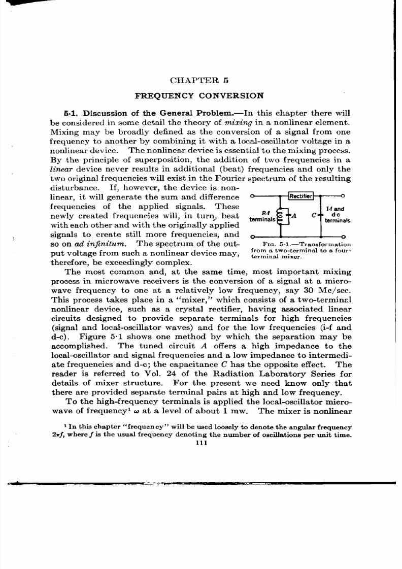
CHAPTER 5
FREQUENCY CONVERSION
5.1. Discussion of the Genera l Problem.—In th is chapter there will
be considered in some deta il the theory of mixing n a nordinea r elemen t .
Mixing may be broadly efined as the conversion of a signal from one
frequency to another by combining it with a loca l-oscilla tor volt age in a
n on lin ea r device. Th e n on lin ea r device is essen tia l t o t he m ixin g pr ocess.
By the pr inciple of superposit ion , the addit ion of two frequencies in a
linear device never result s in addit ional (bea t) frequencies and only the
t wo origin al fr equ en cies will exist in t he F ou rier spect rum of t he r esu lt in g
disturbance. If, however , the device is non-
linear , it will gen era te th e sum and differen ce
n
Rectifier
frequencies of the applied signals. These
I f and
newly crea ted frequencies will, in turn ., bea t ~rm~n~l~ A C ~r~nal~
wit h ea ch ot her a nd with t he or igin ally a pplied
signals to crea e st ill more frequencies, and
so on ad infin itum. The spect rum of the out - Fm. 5,1.—Transformation
fr om a two-t erm in al t o a fOu r -
put volt age from such a nonlinear device may, te,t ina l ~xer ,
t h er efor e, be exceed ingly compl x.
The most common and, a t the same t ime, most impor tant mixing
process in microwave receiver s is the conver sion of a signal a t a micro-
wave frequency to one at a ela t ively low frequency, say 30 Me/see.
This process t akes place in a “mixer ,”
wh ich con sist s of a two-t ermin r.l
non linear device, suc as a crysta l r ect ifier , having associa ted linear
circu it s designed to provide separa te terminals for h igh frequencies
(signal and loca l-oscilla tor waves) and for the low frequencies (i-f and
d-c). F igure 5 1 shows one method by which the sepa ra t ion may be
accomplished. The tuned circuit A offers a high impedance to the
lo a l- scilla tor a nd signa l fr equ en cies a nd a low impeda nce t o in termedi-
a t e frequencies and d-c; the capacitance C has the opposite effect . The
reader is r efer red to Vol. 24 of the Radia t ion Labora tory Ser ies for
details of mixer st ructure. For the presen t we need know only tha t
there a re provided separa te terminal pa irs a t high and low frequency.
To t he h igh -fr equ en cy termin als is a pplied t he loca l-osciUa tor m icr o-
wave of frequency u at a level of about 1 mw.
Th e m ixer is n or din ea r
1In thischapter “ frequenCY”will be usedloosely to denote the angularfrequency
2.f, where~ ie the ueunlfrequency denoting the number of oscilla t ionspsr unit t ime.
111

112
I~REQIJ h’NCYCONVERS1ON
a t th is level and genera tes harmonics no (n = 2,
oscilla tor frequency.
In addit ion th e microwave
[SEC.51
3, .) of the loca l-
signal of fr equency a
is a lso xpplied to the h igh-frequency terminal bu t a t such a rela t ively
low level (usually less than 1 Pw) tha t th ere is negligible genera t ion of
it s ha rmonics .
To be specific, it will be assumed encefor th tha t a > u.
No 1MS of genera lity resu lt s from this assumpt ion . The funct ion of the
mixe is to conver t the si~nal fr equency a to the in termedia te frequency
@ -.. a – o as a resu lt of bea t ing a with u . h ’fany other beat fr equencies
a re genera ted, howev r . The “sum frequency a + o is genera ted with
almost equal efficiency. The frequencies a – o and a + u beat with
a and no to rea te addit ional fr equencies.
These in turn are par t ia lly
conver t ed to fu r ther beat products; t he resu lt ing spect rum is thus
complica ted. Beats between two low-level fr equencies, such as a and
~, can be ignored, however , since the conver sion loss for such a process
is very large. Thus the spect rum consist s of the following frequencies.
(.=(0+/3 (signal)
I
(in t ermed ia te frequency)
At lowlevel . . . . . . . . ~=u_P
(image)
nti+p
(ha rmonic s idebands)
{
At high level . . . . . . . u
nu
(local oscillator)
(h armon ics of t he loca l oscilla tor )
The image frequency u – P is of specia l impor tance in the theory of
mixers; it is denoted here by a specia l symbol -y.
F rom the following discussion , which t rea ts the rela t ive impor tance
of these frequencies, it is apparen t tha t many of them can be ex luded
from fur ther considera t ion . The image and the harmonic sidebands
ca n be ca lled “pa ra sit ic,”
since power consumed t these frequencies is
t aken from the available signal power and the resu lt is to lower con-
ver sion efficiency of the signal to the in termedia te frequency. By
termina t ing th e parasit ic react ively we can insure their minimum power
dissipa t ion . There is another effect of the pa rasit ic which shou ld be
considered in mixer design , namely, th e phase rela t ionship they bea r
to the signal, depending on their t ermina t ion . By roper choice of
r ea ct ive ter mina tion of t he par asit ic we ca n in sur e th at t he in ter media te-
fr equency voltages produced by b at ing of the pa ras t ic with u or nu
add in phase to the direct product of the bea t between w + j3 and u.
These two considera t ions shou ld be kept in mind in the following dis-
cussi m of the rela t ive impor tance of the va r ious parasit ic.
Let
P,
be the power available from the signal sou rce and let G be
the conversion gain from signal t o in termedia te frequency (G is the
r ecipr oca l of t he con version loss L and is usually between 0.1 and 0 3).
SEC.5.1]
DIS C US S ION OF THE GENERAL PROBLEM 113
Then the power available a t in termedia te frequency is GP.. Th is power
must be compared with the power available a t in termedia te frequency
as a result of bea t ing of parasit ic with the local-oscilla tor frequency
or its ha rmonics. The first st ep is to est imate the efficiency of produc-
t io of t he va riou s pa ra sit ic.
As a convenient rule of thumb, adequate
for an order -of-magnitude calcula t ion, it may be assumed that the con-
version gain as a result of bea t ing any frequency with the nth harmonic
nu of the local oscilla tor to form the sum or difference frequency is
about G“. Fa lkoff’ has shown tha t this is roughly t rue for the case
n=2.
First there must be considered the effect of the image sideband
-y = u – ~. This frequency is genera t ed as a result of the direct beat
between signal u + j3 and the second harmonic 2a, and also as a resu t
of the beat between P and a. The first process gives G2P, as
t he power
available at ~, according to our ru le, and the second method also gives
G’P., since the power available at P is GP. and the second beat ing with u
adds another factor of about G. The power at 7 is then of the order of
G’P, and, by beat ing y with u to produce P, anoth r factor of G is added,
with the result that the power available at Q by the indirect path through
~ is of order
GSP..
Next , let us consider the upper harmonic sideband 2W + ~. This
sideband is produced by the direct bea t between the signal co+ 6 and w
Its available power is thus about GP,. The intermedia te frequency P
can be produced by beat ing 2U + P with 2W with a conversion gain of
about Gz. Thus the available power at in termedia te frequency by the
indirect path through 2W + b is about GSP..
It might be concluded from these arguments that the parasit ic
2CJ+ P and ~ – j3 are of comparable importance. This is not t rue,
however . One must consider not only the power but a lso the phase at
in termedia te frequency. If the i-f volt age produced by one of the
indirect paths is in phase with tha t of the direct beat of u + f?with u, the
effect of the parasit ic is grea t ly enhanced. Now the phase at in termedi-
a te frequency is determined by the phase of the parasit ic, which can be
cont rolled t o a cer ta in ext ent by adjust ing t he impedance terminat ing t he
para sit ic a t t he mixer termina ls.
Thk, cont rol is more effect ive at t he
image frequency o – ~ than at the harmonic si eband 2U + @because
of the shunt ing effect of the barr ier capacitance of the crysta l. This
capa cit ance ca nnot be complet ely t uned out beca use of t he ser ies spread-
ing resistance (see Fig. 5.12). Let us consider a typical case. Assuming
the capacit ive reactance of the barr ier equal to 50 ohms a t t i + B and
100 ohms at u – f?, and taking 30 ohms for the spreading resist ance, we
find tha t the impedance tha t can be presented to the barr ier is rest r icted
I D. L. Fa lkoff, RL Repor t No. 95S ,Mar . 11, 1946.

1
114 FR EQUENCY CONVER SION
[SEC.52 !
t o a range of 13.4 in absolu te va lue in the case of – d and to a range
of on ly 4.6 for 2c0 + p. A second reason for the grea t er impor t ance of
u — @ is tha t the i-f impedance of the mixer depends st rongly on the
terminat ion to a – D but only weakly on tha t to 2U + O. The conver se
is t rue for the r -f impedance, but the i-f impedance is, in genera l, t he mor e
cr it ica l fa ct or in r eceiver design .
So far on ly the parasit ic a – P and 2W+ ~ have been considered.
A simila r ana lysis applied to the ot her seco d harmonic sideband 2U – @
and to h igher harmonic sidebands shows tha t they a re rela t ively ineffec-
t ive. The available -f power as a resu lt of the in t erven t ion of these
parasit ic is of order G5P, or less.
It must be concluded tha t the image u – @ is the most impor t an t
parasit ic and tha t specia l a t ten t ion shou ld be paid to it s t ermina t ion in
mixer design . Care should be taken to insu re a nondissipa t ive termina-
t ion a t the ha rmon ic sideband 2U + P, but it does not seem likely tha t
the pa r t icu lar choice of th is termina t ion is of much consequence. The
remain ing parasit ic may be ignored, to a good a ppr oxim at ion , except
tha t in the case of very low loss mixer s it shou ld be insu red tha t their
t ermin a tion s a r e r ea ct ive.
These considera t ions a llow us to ignore a ll parasit ic in the t heory
except u — P, provided tha t it is consisten t ly assumed tha t 20 + ~ is
react ive ly t ermina ted .
The mixing process considered above is not the most genera l tha t
cou ld have been imagined. There migh t , for example, be the case of a
signa l a t o + P and beat ing oscilla tor a t t i/n , i.e., a subha rmonic of u .
The resu lt would be lower conver sion efficiency to @for the same local-
oscilla tor power (and hence the same noise outpu t ), but in the case of
ext remely high frequencies, where it s impract ical or inconvenien t to
provide an oscilla tor at a , this circumvent ion may be used to advantage.
The case of a subharmonic oscilla tor will be considered a ga in in Sec. 5.15,
bu t for the presen t the discussion is confined to an oscilla tor a t ~.
Another possibility not h ither to men t ioned is “ha rmon ic rein force-
mer it , ” which amoun ts to enhancing the effect of the second harmon ic
of the loca l oscilla tor by cor r ect adjustment of it s t ermina t ion or by
deliber at ely n ject in g secon d-h armon ic power fr om some ext er na l sou rce.
Only the fir st method has been resor t ed to in pract ice. The resu lt is to
increase the effect iveness of the pa rasit ic 2U + P and u — ~. Harmonic
r ein for cem en t will be con sider ed br iefly in Sec. 5.14.
5.2. The Admit ta nce Mat rix.-The pr in cipa l object ives in th is ch apt er
a re t o der ive expr ession s for con ver sion loss and for t ermina l impedan ce
of a mixer ; t o show how conversi n loss is rela ted to proper t ies of the
mixer tha t a re simple to measu re; to xamine the effect of the image-
frequency terminat ion on conver sion ; and to show how conversion

I
SEC. 5.2]
THE ADMITTANCE MATRIX
efficiency is rela t ed to the physica l st ructu re of the
t it ula r, t he ph ysica l pr oper ties of cr yst al r ect ifier s.
115
mixer and, in par -
These tasks a re enormously facilita ted by the circumstances tha t
sign al, ima ge, a ndin termeclia te fr equ en cies a re a t su ch lowlevels t ha t t he
rela t ions among their volt ages and cur ren ts a re linear .
It is t rue tha t
con ver sion r esu lt s fr om t he n on lin ea rit y of t he mixer , bu t th is n on lin ea r-
ity affects on ly the loca l-osc lla tor wave and it s in teract ions with the
low-level componen t s; in ter act ions among the low-level componen ts
themselves a re linear to a high degree of accuracy. The mixer , in fact ,
can be rega rded as a linear network with sepa ra te termina ls a t the signa l
fr equency, a t the image frequency, and at the in t ermedia te frequency.
P hysica lly, t he sign al a nd im age t ermin als a re iden tica l, bu t con cedu allv
they may be rega~ded as dist i~ct , since they can be separa t ely lo~ded b;
th e use of sharply r esona nt tu ned circu it s.
Using subscr ipt s a , P, and y to refer , respect ively, t o signa l, in ter -
media te frequency, and image, we can denote by ia , ifl, and iy the com-
plex cu rr en t amplit udes a nd by em ,eR, e,
t he complex volt a ge amplit udes
a t t he t hr ee frequ en cies. We may wr it e t he linea r rela tions bet ween th ese
qu an tit ies a s
‘i. =
Ya ae. + vu ~eii+ ya ~e~,
io = y~=e. + yflpep+ y~Ye?,
J
(1)
~* =
7
Ywea + y~~e~+ yy~e~,
or, in mat r ix form, as
[1 II
ia
e.
i#
=Yefl,
7
e;
(2)
where
(Y7. Y7B Y77J
is the so-ca lled “admit tance matr ix” of the mixer . The aster isk (*)
denotes complex con juga te; it will la t er (Sec. 53) be shown tha the
image curren t and volt age must appear as complex conjuga tes in these
relations.
The admit t ance mat r ix defines all t he conver sion proper t ies of the
mixer . In the genera l form, Eq. (3), it consist s of n ine complex quant i-
t ies (y=., etc.), eigh teen quant it ies in a ll, bu t it will be shown present ly
tha t the number of independen t quant it ies is much smaller-in the
simplest possible case there a re only fou r independent quant it ies in the
admit tance ma tr ix. An immedia te reduct ion in the number of inde-
pendent quant it ies is achieved on the basis of symmetry by in t roducing
the assump ion tha t the mixer is a “low Q‘’ device. By th is is meant

116
FREQUENCY
that there ar e no sharply resonant
CONVERSION
[SEC , 52
circuit s in the mixer l that can dis-
cr imina te between signal (u + P) and image (u — Q), which are close
together infrequency since a>> ~. This assumption isvalidin the case
of most pract ica l mixers and will be adopted throughout this chapter .
On the basis of symmetry between signal a and image ~ we may then
write
Y7R= y%
?/7. = Y:?
Y@?= Y&,
YYy= y:=.
(4)
Conjuga te signs on the r ight a r e necessa ry because the image cur r ent
and volt age ent er into Eq. (2) as complex conjuga tes.
If it is fur ther assumed that ther e is no resonant circuit in the mixer
capable of discr iminat ing between intermediate frequency and direct
cur r en t , it is implied a lso that y8~, the i-f self-admit tance, is real.
This
is expr essed by wr it ing
Yflfl= 9&%
(5)
in conformity with a genera l ru le adopted here that g and b with appropr i-
a te subscr ipts stand, respect ively, for the rea l and imaginary par t s of an
admit tance element . The genera l form for a “low Q” mix r is then
[1
Y.. Y.fi Y.-I
‘f = yflm gpfl y;. .
(6)
Y% Y% Y:.
The number of independent quant it ies has thus been reduced to nine.
Condit ions (4) and (5) for a “low Q” mixer a re int roduced he e as a
resu lt of a plausibility argument .
The y are just ified r igorously in
Sec. 5“3.
A fur ther reduct ion is possible from the fact that we ave at our dis-
posal the or igin of t ime. This fact would be of no help if only a single
frequency wer e involved. In the present case ther e are th r ee frequencies
and the rela t ive phases depend on the t ime t . Let us suppose tha t the
t ime or igin is shift ed, making
t=t’+ to, (7)
where t ’ is the new t ime var iable and h is a constant .
It is clea r tha t
rela t ions bet ween the complex voltage amplitudes cor responding to the
old and the new time zeros are
e~ = ee~”c~+~jfo,
ej = e~ei~fo,
1
(8)
e$ = e#(&~)~O,
1Th is does not imply of cou r se that such circuits a re not a t tached to the mixer
terminals.
I
SEC.52]
where a
THE ADMITTANCE MATRIX
117
pr imed quant ity is measured in the new t ime scale. S milar
rela t ions hold for the cur rent amplitudes. Subst itut ing these rela t ions
in Eqs. (2) and (6), we obta in for the admit tance mat r ix Y’ in the new
t ime sca le
I
y..
y=pf+%
Yayeziuto
Y ! = y~ae–’”’,
!70B
yjap~o
1
(9)
y&e-2j~t0 y~cJ .10 y~a .
Since to is arbit ra ry, it can be chosen to make either yj~, y~a , or Y4Y
real, in any case reducing by one the number of independen t quant it ies,
leaving eight in ll.
A fur ther reduct ion in the number of independent quant it ies is pos-
sible by at t aching to the mixer’s r -f terminals an ideal (dissipa t ionless)
r ansformer . Such a t ransformer is character ized by two parameters
which , for example, might be th posit ion of the r -f t erminals a long a
t ransmission line and a susceptance across these terminals. These two
parameters can be chosen to reduce the number of independent quant it ies
t o six.
This is as far as we can go on purely theoret ica l grounds. A st ill
fur ther reduct ion is possible, however , on empir ica l grounds. The admit -
tance matr ix of a linear passive circuit is well knomm to be symmetr ica l
about its ma in diagona l. If this situa t ion exists in the present case we
have
Y.8 = Y8.,
(lOa)
and
y.r = Y:y,
(lOb)
and it is sa id that
reciprocity h old s.
Exper imen ta lly r ecipr ocit y is found
t o h old for a ll silicon con ver ter s t est ed but not , in gen er al, for germa nium
converters.
Reciprocit y ca nnot be complet ely divor ced fr om hoice of t ime zer o.
Thus if LO# O in Eq. (9), r eciprocit y could hold, for example, in the form
of Eq. (6) for Y but not for Y’.
If it is supposed that the t ime zero has
been chosen to make ya, rea l, Eq. (lOa) alone expresses the condit ion of
reciprocit y; t he second equat ion ( 10b) is redundant .
Since Eq. (lOa)
is a r ela tion between omplex qua nt it ies, r ecipr ocit y imposes two con di-
t ions and reduces the number of independent quant it ies to four . The
t wo condit ions may be writ ten
IYc4 = lYdal,
(11)
and
arg (ya~) = arg (ysa).
(12)
It is a exper imenta l fact that when reciprocity fa ils, as it does for
many germanium crysta ls, t he fa ilure is in Eq. (11) and not in Eq. (12).

118
FREQUENCY CONVER SION
[SEC,
:2
Although ther e isnotheoret ica l explanat ion for th is, Eq. (12) will in tho
grea ter par t of th is chapter be assumed genera lly t rue on empir ica l
gr ou nds. Th isequ at ion expr esses wh at isca lled wea k r ecipr ocit y, wh er ea s
Eqs. (11) and (12) together may be called jull reciprocity. Weak r eci-
procity (a lone) reduces the number of in ependen t quant it ies in ou
b
FIG.5.2.—Equ iva len t lin ea r network of a crys ta l m ixer for which
reciprocity holds.
matr ix to five. It is shown in Sec. 5“5 that these five quan tit ies can be
chosen so as to make the mat r ix rea l, tha t is,
[1
.. 9d 9.7
~=L%I98%
98. ,
(13)
9.7 9.R 9..
and it is a lso shown that , if weak reciprocity does not hold, Y cannot be
wr it t en in real form, whether Eq. (11) holds or not .
It is shown in
Sec. 5.7 that the assumption of weak reciprocity great ly simplifies the
analysis of the effect of image terminat ion on conversion loss.
If full recipr ocity holds, conversion loss can be determined by means
of impedance measurements (see Sec. 7“3). Also, if fu ll reciprocity
holds, the mixer can b represen ted as a linear passive network.
This network is shown in Fig. 5.2. That it in eed epresen t s Eqs. (2)
and (6) with reciprocity can be ver ified in the usual way by supposing
the network to be dr iven from one of the termina l pairs with opposite
pa ir s sh or t-cir cu it ed, a nd t hen con sider in g t he dr ivin g-poin t a dm it ta nce
and the cur ren ts flowing through the shor t -circu ited terminals. This
process must be repea ted for each termina l pair .

119
EC.5.3]
MEASURABLE PARA METERS
THE PHENOMENOLOGICAL THEORY OF CONVERSION
The element s of the admit tance mat r ix define all t he conversion
proper t ies of t he mixer . Dicke and Robert s’ have devised a phenomeno-
logica l t heory of mixers that makes it possible to det ermine all of these
element s from simple measuremen ts at the mixer termina ls without any
knowledge or assumpt ions abou t the in terna l st ructure of the mixer .
The necessary measuremen ts are at loca l-oscilla tor level and do not
requ ire the presence of a signa l.
/
This theory will now be developed.
A physica l t heory of mixers giving ,1
the element s of the admit tance
t
mat r ix in terms of the physica l con -
Rf te rminals
st it ut ion of the mixer is presen t ed
IG. 53.-A mixer con ceived as a “ black-
in Sees. 5“11 to 5“14.
box” wit h r -f a n d d -c t ermin als.
5.3. The Admit tance Matr ix in Terms of Measurable Parameters.—
The mixer is conceived as a “black-box” with r-f and d-c terminals as
shown in Fig. 5.3. Two approximations are made which hold well for
pract ica l mixers .
It is assumed tha t the mixer is “low Q” in the sense
indicated in Sec. 52 and tha t no harmonic voltages appear a t the r -f
terminals. The la t ter assumption does not exclude the presence of
h armon ics in side t he m ixer .
The essent ia l idea of this “black-box” theory is tha t under the above
condit ions r -f (at loca l-oscilla tor level) and d-c voltages can be applied
to the appropr ia te ixer terminals and the effects of the small cur rents
a nd olt ages a t sign al a nd image fr equ en cies r ega rded a s sma ll va ria tion s
of the loca l-oscilla tor cu rren t and voltage; similar ly the i-f cu rrent and
volt age ca n be r ega rded as small var ia tion s of t he d-c cu rr en t and volt age.
Let us, a ccor din gly, su ppose t ha t t he black box of F ig. 5.3 has volt age
and currents at it s two terminal pairs given by the following scheme.
R-f t ermina ls
D-c t erm ina ls
Voltage
Re (e le~w’)
e.
Current
Re (i,e~”’)
io
Th e followin g n ot at ion will be u sed.
Y ~ Uei = r -f admit ta nce of t he mixer a t loca l-oscilla t or level.
lell = absolu te value of el.
ef = complex conjugate of e1.
1R. H. Dic e and S. Robert s, “Theory of Radar Mixers,” RL Repor t No. 61-5,
J uly 15, 1942; an d R. H. Dicke, “ A Recipr ocity Th eor em an d It s Applicat ion t o t he
Meseu rem en t of Ga in of Micr owa ve Cr yst al Mixers,” RL Repor t No. 61-18, Apr . 13,
1943. See a lso R. N. Smith , “The Theory of h lixers in Terms of Measurable Mixer
Con st an ts,” NDRC 14-259, P ur du e U., Ma r. 24, 1944.
120 FREQUENCY CONVER S ION
[SEC.5.3
The curr ent s flowing at t he t erminals will be funct ions of t he volt ages
of the forml
~0 = Meolled))
(14a)
il = ely(eO,lell).
(14b)
Different ia t ing Eq. (14) with respect t o a , % and ef, we obt~n
If there is added to Eqs. (15) the complex conjuga te of the second
of these equa t ions they will have the fo m of a three-t srmina l-pa ir
network.
If t he t ime zero is chose so that de, is rea l, Eqs. (15) have
the form of a two-terminal-pa ir net work. It is usually more convenient ,
however , to choose the t ime zero so that el is rea l.
There is now i t roduced the signal volt age e. and the image voltage e~
a s differ en t ia ls of t h e loca l-oscilla t or volt a ge el.
Th e physica l r -f volt age
will be
Re [(cl + de, )ei”’] = Re (ele’m’) + Re (dele~w’). (16)
If we then put
d el = e=e’fl’ + eye–’b’,
(17)
the r-f volt age is seen to be composed of th ree par t s:
Re (e ,e id’)
(local oscillator)
+Re (e .e ic”+~)’)
(signal)
I
(18)
+Re (e ,e~f”–~)’)
(image).
It has been assumed tha t these a re the only voltages appear ng at the
r-f terminals. Tha t is, ha rmonic voltages at these terminals, a lthough
n ot n ecessa rily in side t he m ixer , a re n eglect ed.
In a simil~r way the i-f volt age ed c~n be int roduced s a different ia l
of the d-c bias voltage eo a t the d-c termina ls.
The volt age at these
termina ls wi l then be
eo + deo,
(19)
where
det i = Re (e~e@’)
(i-f volt age). (20)
In the same manner the cur rent s a t signal, image, and intermedia te
fr equ en cies a re in tr odu ced a s differ en tia ls of t he loca l-oscilla tor cu rr en t
il and the d-c cur rent iO:
1 It is clea r t ha t t he d ir ect cu r r en t io and the r -f admit t ancey a re independen tof
the t ime or igin and therefore depend on the absolute value of e, but not on its phase.

SEC. 5.4]
TRANSFORMATION TO NEW VARIABLES
121
dil = i~e@’ + i7e–@’;
(21)
d io =
Re
(i@e’@’).
(22)
Using Eqs. (17), (20), (21), and (22) and separa t ing th e differ en t t ime
factors, we obta in f om Eq. (15)
These equat ions a re observed to have the same form as Eq. (1). As
expected, the symmet ry rela t ions [Eqs. (4) and (5)] for a “ low Q” mixer
hold. Compar ing coefficien t s of Eqs. (1) and (23) we find
?4.. = y + ~ Ie,l *,J
(24a)
1 ay
ymD= ~ e, a~OJ
(24b)
1 e; ay
‘“7 = 2~81e,l’
(24c)
““ = &
a~,l’
(24d)
aio.
9B0 = ~.
(24,)
Let us choose the ime zero so tha t el is rea l; Eqs. (24) then become
We note tha t the loca l-oscilla tor admit tance is now given by
y = y.. – y.,.
(26)
5s4. Tr an sforma tion of t he Ma tr ix t o New Va riables.—All t he pa ram-
eter s on the r ight -hand side of Eq. (16) a re direct ly measurable except
for the r -f voltage e,. In pr inciple el could be found by measur ing the
r -f power P and the mixer conductance g.
It is more convenien t , how-
ever , t o t r an sform Eqs. ‘(25) t o n ew independen t va ria bles P and V, w ere
P = +ge~
(27a)
122
FR EQUENCY CONVERS ION
[SEC.
5.4
isthe r -f power delivered to the mixer and
V = e,. (27b)
Although is ident ica l with e,, it is dist inguished ith a new symbol
to avoid explicit st a tement of wha t is held constant in par t ia l differen-
tiation.
Thus ~/i e, implies tha t e, is held const ant ; d/ dV implies t h at P
is held constant . The t ransformat ion from el to P is useful sin ce P is
direct ly mea surable, wh er ea s el is not .
In fact , the value of e, is some-
wha t a rbit ra ry, since it depends on the defin it ion of the line impedance. 1
If X is some dependent var iable, then we have the genera l par t ia l
d ifferent ia l re la t ions
ax
axav
av=+gg)
.—
deo
(28)
ax
:;g+a;g.
—
ael
(29)
Subst itut ing Eqs. (27a) and (27b) in Eq. (28), we have
ax ax
—
deO –
~+?-%G.
g de. ap
If X = gin Eq. (30),
where
Subst itut ing Eq. (31) in Eq. (3o), we obta in
ax ax Plagax
—+ B; WFP”Z=av
Subst itu t ing Eqs. (27a) and (27b) in Eq. (29) yields
ax
—.
ael
( )
iP+; g 8$.
If X = gin q. (34),
(30)
(31)
(32)
(33)
(34)
(35)
1 It sh ould be not ed h er e tha t y a nd its der iva t ives a re a lways mea su red in t erms of
the cha racter ist ic admit t ance go of the r -f t ransmission line. Since, in the case of a
wavegu ide, t h er e is n o un iqu e defin it ion of g~,t h e a ct ua l va lu e of y in ohms is s omewha t
ambigu ou s. This, h owever , occa sion s n o r ea l difficu lt y. Th e pr oper ties of t he m ixer
wit h wh ich we sh all be con cer ned a re its t ermin al im peda nces a nd it s con ver sion loss.
The la t ter is a pure number and so is independen t of the unit s used; the former will
a lways be given in terms of g, a t the r -f end, and will be independent of O, a t the
i-f en d.
SEC. 5.4]
TRANSFORMATION TO NEW VARIABLES
123
Subst itu t ing Eq. (35) in Eq. (34) yields, fina lly,
Equat ions (33) and (36) make it possible to t ransform Eqs. (25) a t once
t o t he n ew in depen den t va ria bles
P
and
V.
The following abbrevia t ions
will be u sed:
The t ran sformed Eqs. (25) becom e (y@. is n ow real becau se of th e choice
of t im e zer o)
where
and
where
and
b
mm;
yb = go. =
D
(38)
(39)
WI = g.p +
jb.p,
(40)
(41)
9.==9+~9P=&
(44)
baa=b+~bp;
(45)
Ycq = gay + h,
(46)
where
()
a7=~9P=g&–1’
(47)
In the preceding set of equat ions the quant ity
D is given by Eq. (32).
Equat ions (38) through (48) give all the elements of the mixer matr ix

124 FR EQUENCY CONVER S ION
[SEC.55
in t erms of dir ect ly m easur able qu ant it ies.
In Sec. 5.7 these equat ions
a re u sed t o der ive expr ession s for con ver sion loss a nd m ixer a dmit t an ces.
6.5. Reciproci@.—In Sec. 5“2 recipr ocity was defined and it s impor-
tance in mixer theory poin ted out .
Recipr ocit y ha s been t e t ed exper i-
menta lly with th e aid of th e expressions der ived in the pr ecedin g sect ion .
Before descr ibing these test s the g nera l subject of reciprocity will be
discu ssed in mor e det ail.
In Sec. 5.2 it was shown that the equat ions expressing reciprocityy
depend on the choice of t ime zero.
Equ at ion s (10) expr ess r ecip rocit y
provided the t ime zero is chosen to make ya , rea l. A more genera l
expr ession , va lid for a ny t ime zer o, is obta in ed by a pplyin g t he con dit ion
of symmetry about the main diagonal of the mixer matr ix to the genera l
expression , Eq. (9), for th e matr ix.
We obt ain
where tos an arbit ra ry constant .
Eliminat ing t , between Eqs. (49) and
(5o), we obta i th e t wo condit ions
lYa dl = IYA
(51)
and
arg ya~ = arg yfl. + arg y.~.
(52)
We observe tha Eq. (51) is ident ica l with Eq. (11). Equat ion (52)
expr esses t he gen er al con dit ion of
weak reciproci ty
and reduces to Eq. (12)
wh n arg yay
= O. A sta tement of weak reciprocity a lterna t ive to
Eq. (52) is Im (y.Py&y&) = O.
Dicke 1 has shown that ju ll reciprocity holds if t h e following condit ion s
are sa t is fied :
. Th e ph ase of t he elect ric field is con st an t over t he r ect ifyin g ba rr ier ,
th at is, t he m et al-sem icon du ct or ju nct ion of t he cr yst al r ect ifier .
2. There exist s a t ime zero with respe t to wh ch the elect r ic field a t
the ba rr ier is an even funct ion of t ime.
To these condit ions must be added a th ird not explicit ly sta ted by
Dicke, a lthough it is implied in his proof:
3. The elect r ic charge on the barr ier is a linear funct ion of the barr ier
voltage.
Con dit ion 3 exclu des t he possibility of a va ria ble ba rr ier ca pa cit an ce.
Condit ions 1, 2, and 3 together a re sufficien t for re iprocity and 3 at
least is necessary. It appears, however , (see Appendix A) tha t Condi-
t ion 2 may be weakened by replacing the word “even” by “ even or odd.”
I R. H. Dicke,
“ A Recipr ocit y Th eor em a nd It s Applica tion t o t he Mea su rem en t
of Ga in of Micr owa ve Cr yMa l Mixer s, ” RL Repor t N o, 61-1$, Apr . 13, 1943.
SEC.53]
kECII’ROCI TY
125
Th e “r ecipr ocit y t heor em ”
of Dicke is given in Appendix A.
It is
proved there tha t , under the above condit ions, Eqs. (49) and (50) a re
f
sa t isfied when h is the t ime zero of Condit ion 2.
f the th ree condit ions for reciprocity only the fir st can be expected
to hold to a good approximat ion .
Th e secon d con dit ion implies eith er
a bsen ce of h armon ic volt ages a t t he ba rr ier or t he exist en ce of cer ta in ph ase
rela t ionships between ha rmonics and the fundamenta l. The th ird condi-
t ion may be approxima tely t rue for silicon rect ifier s but it is known tha t
t he ba rr ier ca pa cit an ce of germa nium r ect ifier s is decidedly va ria ble wit h
bar r ie r voltage.
t
However th is may be, it is a fact tha t fu ll r eciprocity is closely fu l-
filled for silicon cryst a ls and, a lthough it fa ils for many german ium
cryst a ls, weak reciprocity holds for all crysta ls t est ed, silicon and ger -
manium. Exper imenta l t est s of r eciprocity have been made by Smith ,’
who measured the element s of the admit tance ma tr ix by means of
Eqs. (38) to (48) which give the mat r ix elemen t s in terms of measurable
pa rameter s. To find the form of the reciprocity rela t ions in these
var iables, we fir st con sider Eqs. (24). Th e wea k-r ecipr ocit y con dit ion ,
q. (52), a plied t o these equa t ions gives, if 4 is the phase of el,
or
a~
ay
arg Xi = arg ml “
Now any genera l var ia t ion in y is given by
ay
ay
dy = ~, de, + ~1 dlell
or , in the new var iables, by
ay dP.
y=$dV+z
(53)
(54)
(55)
According to Eq. (53) ay/ae, and t )y/a Ie,l have the same phase. It
follows then from Eq. (54) tha t a ll va r ia t ions in y withou t r ega rd to
cause must have the same phase.
Hence, from Eq. (55),
a rg #v = arg #
(56)
~
This is the form tha t the weak reciprocity condit ion takes in the new
var iables. If we put y = g + jb and use the abbrevia t ions of Eq. (37),
/
1R. N. Smit h, “Th e Th eor y of Mixers in Terms of Measu ra ble Mixer Const an ts, ”
NDRC 14-259, Purdu e U,, Mar. 24, 1944.
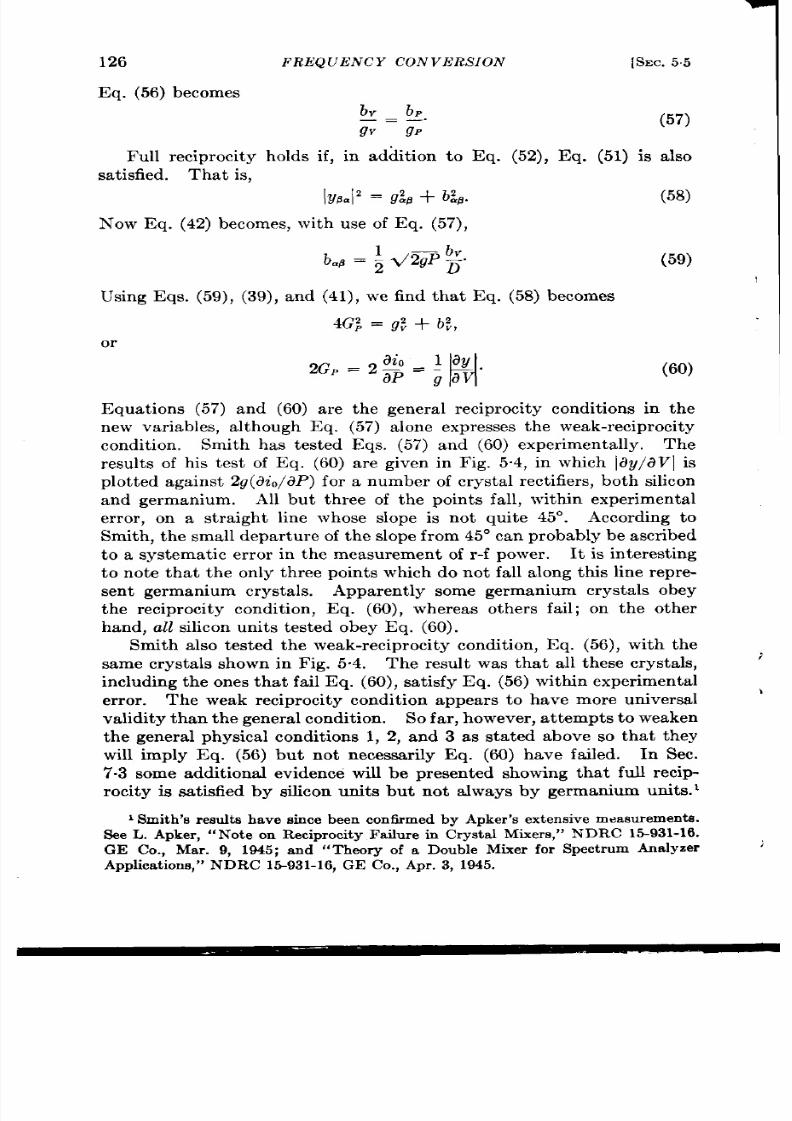
.
126
Eq. (56) becomes
Fu ll r ecip rocity
sa t isfied. That is,
FR .EQ(J IiN CY CONVER SION [SEC.55
b. =fh’.
$ g,
(57)
holds if, in addit ion to Eq. (52), Eq. (51) is a lso
I?4P.I=
9i9
+ %.
(58)
Now Eq. (42) becomes, with useof Eq. (57),
(59)
Using Eqs. (59), (39), and (41), we find that Eq. (58) becomes
4Gj = ; + b~ ,
or
2Gp=2~; =-
bl
lay.
(60)
ga
Equat ions (57) and (60) a re the genera l r eciprocity condit ions in th
new variables, a lthough Eq. (57) a lone expresses the weak-reciprocity
condit ion , Smith has tested Eqs. (57) and (6 ) exper imen ta lly. The
resu lt s of his t est of Eq. (60) a re given in Fig. 5.4, in which 18y/8V] is
p lot t ed aga in st 2g(8i0/ 8P) for a n umber of crysta l rect ifiers, both silicon
and germanium. Ml but th ree of the points fall, with in exper imen ta l
er ror , on a st ra igh t line whose slope is not quite 45° Accordin to
Smith , the small depa r tu re of the slope from 45° can probably be ascr ibed
to a systemat ic er ror in the measurement of r -f power . It is in terest ing
to note tha t the on ly th ree poin ts which do not fall a long th is line repre-
sen t german ium crysta ls. Apparen t ly some germanium crysta ls obey
the reciprocity condit ion , Eq. (60), whereas others fail; on th other
hand, ll silicon un its t ested obey Eq. (60).
Smith also test ed the weak-reciprocity condit ion , Eq. (56), with the
same crysta ls shown in Fig. 5.4. The resu lt was tha t all these crysta ls, ;
in clu ding th e on es th at fa il Eq. (60), sa t isfy Eq. (56) with in exper im en ta l
er ror . The weak reciprocity condit ion appea rs to have more un iversa l ‘
va lidit y t han t h e gen er a l condit ion .
So fa r, h owever , a ttem ts t o wea ken
the genera l physica l ondit ions 1, 2, and 3 as sta ted above so tha t they
will imply Eq. (56) but not necessar ily Eq. (60) have fa iled. In Sec.
7.3 some addit ional evidence will be presen ted showing that full r ecip-
rocity is sa t isfied by silicon units but not a lways by germanium nits.’
1 Sm it h’s r esu lt s h ave sin ce been con tirmed by Apker ’s ext en sive m ea su rem en ts.
Se L. Apker , “Note on Reciprocity Fa ilure in Crysta l Mixer s,” NDRC 15-931-16.
GE Co., Mar . 9, 1945; and “Theory of a Double Mixer for Spect rum Analyzer )
Applica tion s,” NDRC 15-931-16, GE Co., Apr . 3, 1945.
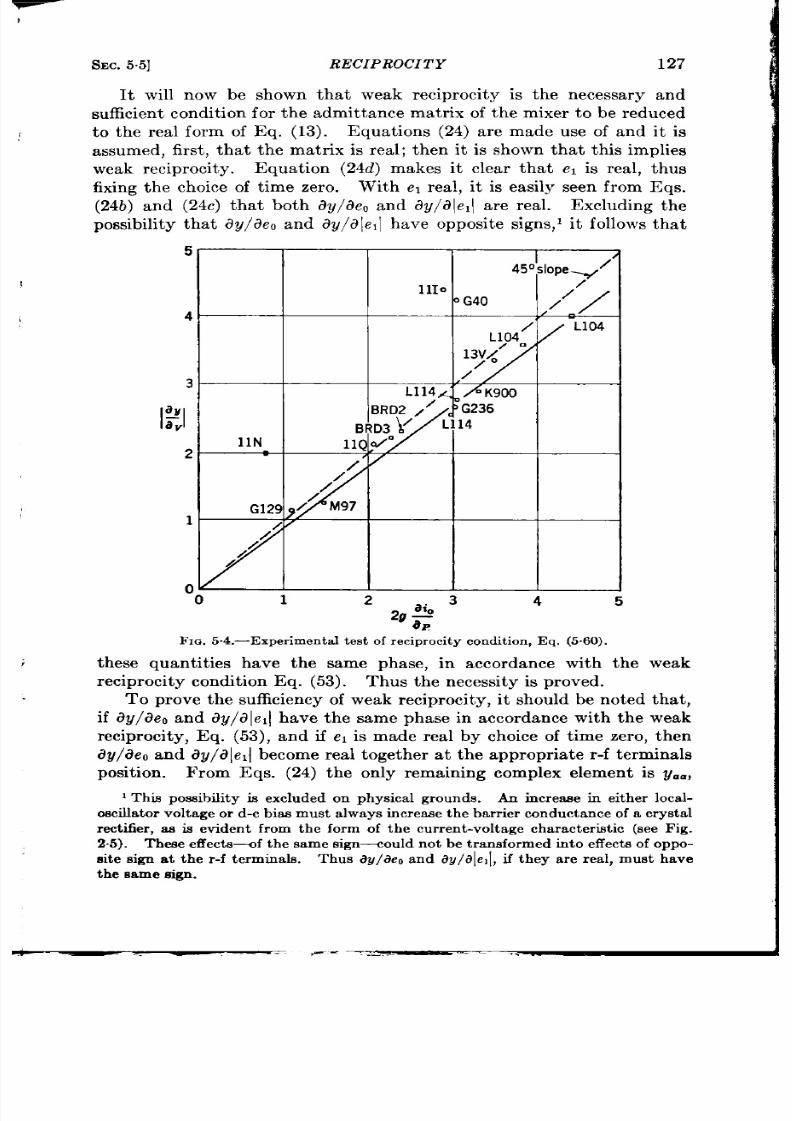
I
SEC.5.5]
It will now be shown
RECIPROCITY
127
that weak reciprocity is t e necessary and
sufficien t condit ion for the admit tance matr ix of the mixer to be reduced
to the rea l form of Eq. (13).
Equat ions (24) a re made use of and it is
assumed, first , tha t the matr ix is rea l; then it is shown tha t this implies
weak reciprocity. Equat ion (24d) makes it clear tha t el is rea l, thus
fixing the choice of t ime zero. With el rea !, it is easily seen from qs.
(24b) and (24c) tha t bo h @/de~ and dy/~le,{ a re rea l. Excluding the
possibility tha t dy/~eO and &y/dle,l h ave opposite signs,l it follows that
5 “
)
45”
slopey
/
llIcI
o G40
4
//<’/ -
L104
13)V
/
Ll14~
~ K900
l%;
BRD2 /’
llN
2 -
/
n
-o 1 2 3
4 5
29:
FIG. 5 .4 .—Exper imentcJ test of reciprocity condit ion , Eq. (5 .60).
these quantit ies have the same phase, in accordance with the weak
reciprocity condit ion Eq. (53). Thus the necessity is proved.
To prove the sufficiency of weak reciprocity, it shou d be noted tha t ,
if ~y/deo and 13y/d Iell have the same phase in accordance with the weak
reciprocity, Eq. (53), and if el is made rea l by choice of t ime zero, then
dy/c3e0 a nd dy/d Iell becom e r ea l t oget her a t t he a ppr opr ia te r -f termin als
posit ion . From Eqs. (24) the on ly remaining complex elemen t is y..,
1 This possibility is excluded on physica l gr ounds. An increa ze in either loca l-
oscilla tor volt a ge or d -c ia z must a lways in cr ea se t he ba rr ier con du ct a nce of a cr yst al
r cet ifier , as is eviden t fr om t he form of t he cu rr en t-volt age cha ra ct er ist ic (see F ig.
2.5). These effects-f the same signaould not be t ransformed in to effects of oppo-
site sign a t t he r -f t er mina ls.
Th us a y/a eO a nd aY/ a lg, l, i f they a re rea l, must ha e
t he same sign .
—-
128
FREQUENCY CONVER SION
[SEC.5.6
which can be made real by adding a suscepta ce a t the r -f termina ls to
cancel the imaginary par t of y [see Eq. (24a)]. The addit ion of sus-
ceptance does not a ffect any parameter of the matr ix other than W.=.
The whole matrix thus becomes re l.
It is notewor thy tha t , if the t ime zero is chosen to make e, rea l and
posit ive, and if the r -f terminals a re located where ~y/de~ and dy/dle,l
a re rea l and posit ive, and if y~a is ma e rea l by addit ion of a susceptance,
every element of the matr ix is not on ly rea l, but rea l and posit ive. In
th is case the r-f terminals a re sa id to be at the “ s tandard posit ion . ”
The standard posit ion has a per iodicity of one-half wavelength along the
r -f t ra nsm ission lin e.
CONVERSION LOSS AND MIXER ADMITTANCES
5.6. Genera l Defin it ion of Loss; Specia l Cases.—Following Fr iis, I
con ver sion loss is defin ed as t he r at io of t he a va ila ble in pu t (sign al) power
to the available ou tpu t (i-f) power .
Th is defin it ion mak es con ver sion
loss depend on the r-f load admit tance (i.e., the in terna l admit tan e of
the signal source) as well as on the proper t ies of the mixer (i.e., th mixer
a dm it ta nce mat rix).
In some respect s th is is unfor tuna te, since it is
desirable, for specifica t ion purposes, to be able to assign to a crysta l
con ver ter a n umber ch ar act er izin g its con ver sion efficien cy.
It is pos-
sible, however , to define specia l r -f load admit tances in erms of the
elements of the admit tance matr ix.
The cor responding values of con-
ver sion loss a re th en cha racter i t ic of t he mixer .
For example, let us suppose t a t t e r -f circuit a t tached to the r f
mixer terminals is broadly tuned in the sense that it presen ts the same
load admittance to the image frequency as to the signal fr equency.
This is ca lled the” broadband case. ” Under th is condit ion , there may be
defined at least two specia l va lues of the conversion loss tha t depend
only on the mixer matr ix. The first , denoted here by Lo, is the con-
version loss when the load admittance, common to signal and image, is
adjusted to match (i. e., t o be the complex conjuga te of) the admit tance y
r
of the mixer to the loca l-oscilla tor wave.
Now LO is not the minimum
loss in the broadband case. It will presen t ly be shown, however , tha t a ‘
denoted by Lz. In the next sect ion it will be seen tha t
LO
and Le are
near ly equal. In
acceptan ce testin g of mixer crysta ls, it is LO tha t is
mea su r ed and specified .
1H. T. Fr iis, “Receiver Noise F igures,” BTL Repor t MM*160-39, May 13,
1942; and P roc. I. R . E., 32, 419 (1944).
2 This minimum will a lways exist provided there is exclu ded the possibility of
nega t ive i-f conductance. Crysta ls exhibit ing nega t ive i-f conductance under cer ta in ‘,
r -f tun ing condit ions have recent ly been made by H. Q. Nor th , however . Such caaes ‘
a re exclu ded fr om t he pr esen t discu ssion a nd a re t rea ted sepa ra tely in Ch ap. 13.
,
,
SEC.5.6]
Other
GENERAL DEFIN ITION
values of loss would not
fa ct th at few micr owa ve receiver s
OF LOSS ; S PECIAL CASES
129
requir e defin it ion were it not for the
actua lly opera te under condit ions of
broadband r-f tuning. In microwave receiver s, the signal is fed to the
mixer th rough a TR (t ransmit -receive) switch .
This resonan t cavity
pr sent s (approximately) a match to the mixer a t signal frequency. In
the case of a na rrow-band TR switch (the usual case), however , the
impedance at the exit window of the TR switch at the image frequency
is a good approximat ion to a shor t circu it .
If the mixer is ma tched at
signal frequency to the conductance go of the line connect ing it with the
TR switch t en , under usual condit ions, the TR switch will presen t an
admit tance go to the signal (f equency m) and an admit tance
“ = ’ J ’ + ’ Q( %- 9 1
t o neighbor ing frequencies u .
Here Q is the “loaded Q” of the TR
switch , a typica l va lue of which is 250. If the signal fr equency is, let us
say, 3000 Me/see and the in termedia te frequency 30 Me/see, the image
frequency will be 2940 Me/see and Y(Q = 250) for the image will be
go(l – jlo)—which is a fa ir approximat ion to a shor t circu it . The
approximat ion will not be as good a t h igher signal frequencies for the
same in t ermedia te fr equ en cy.
If we t ravel down the line from the TR
switch to the posit ion where the admit t nce matr ix of the mixer becomes
r ea l (th e standa rd mixer terminals), th e sh or t circu it will be t r an sformed
at th is poin t to some genera l susceptance which can be made near ly a
sh or t circu it or n ea rly an open circu it by pr oper ‘(lin e-st retch ing. ”
Thus it is necessa ry to examine the sepa ra te dependence of con -
version loss on signal load and on image load admit tance.
There a re
two reasons for th is. We wish to see, fir st , how the specified loss LO
compares with the loss under opera t ing condit ions and, second, wha t
benefit , if any, can be der ived from the fact tha t we have at ou r di posa l
two load admit tances nstead of on ly one.
In t rea ting th is pr oblem (see Sees. 5.8 an d 5.9) h e image term n at ion
will be assumed fixed at some arbit ra ry value, and the dependence of
loss on signal load admit tance alone will be studied. It will be shown
tha t the loss has a unique minimum value in genera l (see the preceding
footnote) as a funct ion of signal load admit tance. This value of loss is
design at ed by Lm .
The depen dence of on image terminat ion is then
studied (see Se . 5.9). At the standard r-f termina l posit ion , tha t is, the
posit ion for a rea l admit tan ce matr ix, th e loss Lm has specia l va lu es L1 for
sh or t-cir cu it ed im age termin als, a nd j for open -cir cu it ed im age t ermi-
nals. The lesser of LI and L ~ k shown to be the sm allest possible valu e
of loss u nder a ny con dit ion s of r -f t un in g.
It is a lso shown that , for some
crysta ls, a value of image load admit tance, rea l a t the standard r-f
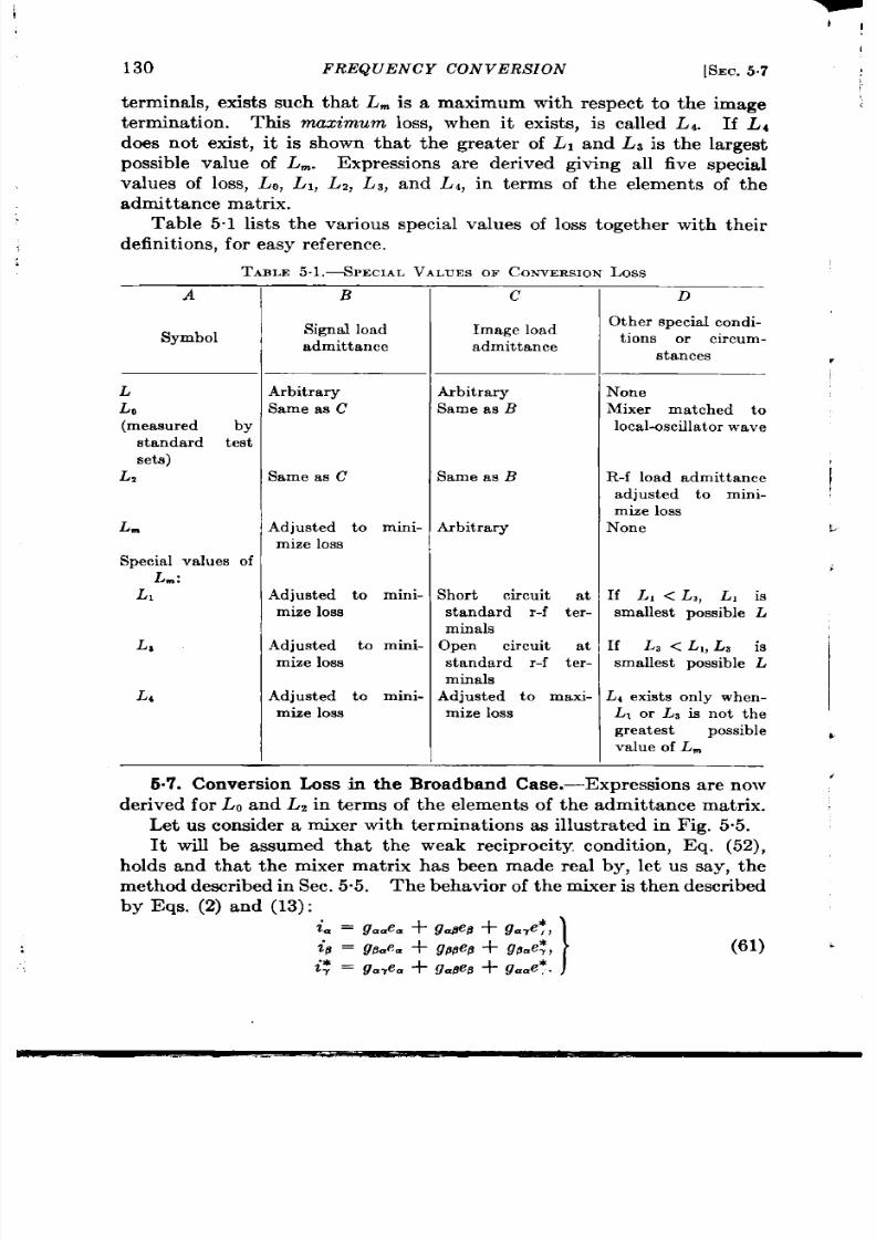
130
FREQUENCY CONVERS ION
[SEC.5.7
t ermina ls, exist s such tha t L~ k a maximum with respect to the image
ter rn in at ion . This nwzimum loss, when it exist s, is ca lled L1. If L,
does not xist , it is shown tha t the grea t er of L, and L, is t he la rgest
possible va lue of L~. Expressions a re der ived giving a ll five specia l
va lu es of loss, LO, Ll, Lz, Ls, and L i, in t erms of the elemen t s of the
a dm it ta nce mat rix.
Table 5.1 list s the va r ious specia l va lues of loss together with their
defin it ion s, for ea sy r efer en ce.
TABLE5.1.+ PECIALVALUESOF CONVERSIONoss
A
Symbol
L
L,
(measured by
standard test
sets)
L,
L.
Specia l va lu es of
L
III:
L,
L,
L,
B
Signa l load
admittance
Arbitrary
Same as C
Same as C
Adjust ed to mini-
mize loss
Adjust ed to min i-
mize 10s s
Adjust ed to mini-
mize loss
Adjust ed to mini-
mize 10s s
c
Image load
admittance
Arbitrary
Sam e as B
Same as B
Arbitrary
Short circ it at
standard r -f ter -
minals
Open circu it at
standard r -f ter -
minals
Adjust ed to maxi-
mize loss
D
Other specia l cond i-
t ions or circum-
stances
v
None
Mixer matched to
local-oscillator wave
R-f loa d a dm it ta nce
adjusted to mini-
mize l ss
None
If L, < L,, L, is
sma lles t pos sible L
If L, < L,, L, is
sma lles t pos sib le L
L, exist s on ly wh en -
L, or L, is not he
greatest
possible
va lu e of L~
507. Conversion Loss in the Broadband Case.—Expressions a re now
der i ed for LO and Lz in ter s of the elemen ts of the admit tance matrix.
Let us consider a mixer with terminat ions as illust rated in Fig. 5.5.
It will be assumed that t he weak reciprocity, condit ion , Eq. (52),
holds and that the mixer mat r ix has been made real by, let us say, t he
method descr ibed in Sec. 5.5. The behavior of the mixer is then descr ibed
by Eqs. (2) and (13):
i= = g.ae= + 9Z8 + 9.,e?,
i~ = gd.e= + gp~efl + gpme~,
)
(61)
& = g.~ea + g=,9e~+ g=Oe*.
v
,
.

SEC.5.71
CONVERS ION LOS S IN THE BROADBAND CASE
131
In Fig. 5.5wehave acurren t source of peak st rength A a nd in ter na l
:,1
con du ct an ce ga a tt ach ed t o t he sign al t ermin als.
The-same conductance
ga will be considered to load the image terminals. The available input
signal power is, then,
~,=g
*
8g.”
(62)
To find th e a a ilable ou tput power we fir st find t he i-f con ducta nce g5
of t he mixer
We have, from Fig. 5.5 (suppressing A),
i. =
– g.ea,
i* = –gae~,
7
1
(63)
i~ = g~e.g.
Subst itu t ing Eq. (63) in to Eq. (55), we get th ree homogeneous equa-
t ions in ea , ep, and e;, the determinant of which must vanish for con-
L7
i
m
5
ea
T
9=+
D
Mixer — gp e~ gb
i~
e?
u
9.
FIG.5 .5 .—Mixer -te rmina l condit ions in the broadband case.
sistency. Solving for gp, we find
2gm8g8=
90 = 986 –
g.. + g., + %“
(64)
The i- cu rr en t ip flowing in to a sh or t circu it (gb = cc) is n ext fou nd.
In Eq. (61) we put
e~ = O,
A ia + goes,
“* = –g.e~,
lY
a nd solve for
ip .
We get
AgE.
ifl =
9.. +
g., + g.”
The available outpu t power will then be
Pm = 3.
‘“
$-%9
(65)
(66)
.-—
‘- ——
- —.....
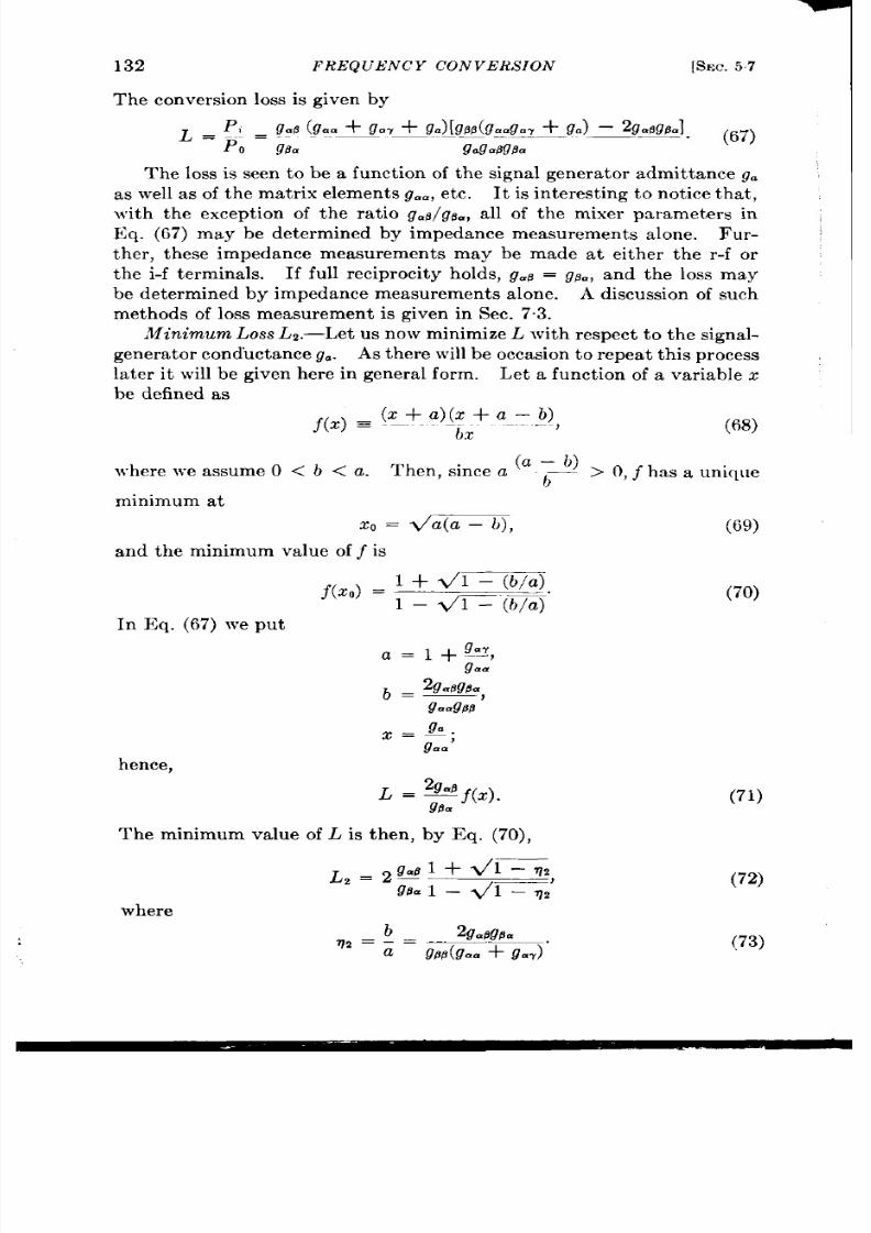
132
FR EQUENCY CONVER S ION
[SEC.57
The conversion loss is given by
The loss is seen to be a funct ion of the signal genera tor admit tance g=
as ell a s of t he mat rix elemen ts gt it i,et c.
It is in terest in g t o n ot ice th at ,
~vith the except ion of the ra t io g.d/g6a, all of the mixer parameters in
Eq. (67) may be determined by impedance measurements a lone. Fur-
ther , these impedance measurements may be made at eit er the r -f or
the i-f terminals. If fu ll reciprocity holds, gap = gpa, and the loss may
be determined by impedance measurements alone. A discussion of such
methods of loss measurement is given in Sec. 7.3.
Minimum Loss L,.—Let u s n ow m in im ize L with respect t o the signal-
genera tor conduct ance g.. s there will be occasion to repea t th is process
la ter it will be given here in genera l orm. Let a funct ion of a var iable z
be defined as
~(z) ~ (<+_ :)f: .+ a – ~),
bz
~vhere we assume O < b < a.
Then, since a
(a –-) >0 ~ has a ,ln iq,,e
b’
(68)
minimum at
Z, = /a(a – b),
(69)
and the minimum value off is
j(xo) =
l+vl– (l@.
1 – <1 – (f)/a)
In Eq. (67) we ‘--’
uu
~=l+g”fl,
f?..
~ _ 29.89R.
9-9!M ‘
~=9J.
9.- ‘
hence,
Th e m in imum
where
va lu e of L is then , by Eq. (7o),
(70)
(71)
(72)
(73)
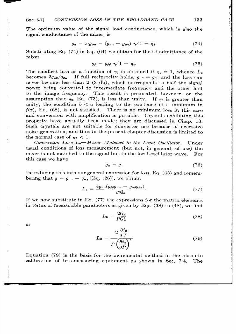
SEC.57]
CONVERS ION LOSS ’ IN THE BROADBAND CASE
133
The optimum value of the signal load conductance, which is a lso the
signal con du cta nce of th e m ixer , is
g. = Xog.a =
(9.. + ga-r)dl – ?2.
(74)
Subst itu t ing Eq. (74) in Eq. (64) we obta in for the i-f admit tance of the
1
mixer
I
9!5 = 988 V’1 – 72.
(75)
The smallest loss as a funct ion of Tlzis obta ined if qz = 1, whence L2
becomes 2g.@/g@.. If fu ll reciprocity holds, gt i~ = gp. and the loss can
never become less than 2 (3 db), which corresponds to half the signal
power being conver t ed to in termedia te fr equency and the other ha lf
to the image fr equency. This result is predica ted, however , on the
assumpt ion that qt , Eq. (73), is less than unity.
If qz is grea ter than
unity, the condit ion b < a leading to the existence of a minimum in
f(z), Eq. (68), is not sa t isfied.
There is no mi imum loss in th is case
a nd con ver sion wit h amplifica tion is possible.
Cr ysta ls exh ibit in g th is
proper ty have actually been made; th ey a re discussed in Chap. 13.
Such crysta ls a re not suitable for conver ter use because of excessive
noise genera t ion , and thus in the presen t chapter discussion is limited to
the normal case of T2 < 1.
Conversion Loss LO—iWixer hfatched to the Local Oscillator.—Under
usual condit ions of loss measurement (bu t not , in genera l, of use) the
mixer is not ma tched to the signal but to the loca l-oscilla tor wave.
For
th is case we have
g. = g.
(76)
In tr odu cin g t his in to ou r gen er al expr ession for 10SS,E q. (63) a nd r em em -
ber ing tha t g = g.. –
g=~ [~~q. (26)], ~ve obtain
(77)
If }ve now subst itu te in Eq. (77) the expressions for the matr ix elemen ts
in terms of meas rable parameters s given by Eqs. (38) to (48), we find
2Gv
Lo = ~Gj
or
(78)
(79)
Equat ion (79) is the basis for the incrementa l method in the absolu te
ca libra t ion of loss-measur ing equ ipment as showm in Sec. 7.4. The

—
134
FREQUENCY CONVER SION
[SEC.5.7
validity of Eq. (79) does not depend on full r eciprocity, nor even on weak
reciprocity, although the la t ter was assumed in its der iva t ion . This
st a tement may be ver ified by assuming a matr ix of the genera l form of
Eq. (6), in which no assumpt ions about reciprocity are made; Eqs. (77),
(78), and (79) remain valid even if both reciprocity condit ions fail.
However , LO is not the minimum loss obta inable under broadband r-f
tuning condit ions. In fact , Lo z L,, where L, is given by Eq. (70).
Since
Lo
is the par t icular value of loss specified to be measured in
accept an ce test ing of crysta ls, it is well t o h ave an est imate of t he amount
by which it exceeds the minimum loss Lz. The opt imum value of ga is
z~.., as given by Eq. (72). If we pu t g. = Cz,g=a into Eq. (63), the
la t ter r educes t o
where
(80)
Now C is the ra t io of the actual signal-genera tor conductance to the
(C+ l)’. h
opt imum value and
-lC
1s t e usual mismatching factor .
In addi-
(---)
l–c’
t ion to th is, however , there is the factor 1 – -
L;’ l+C
~wh ich is less
(1 + c)’.
than unity, a lthough much closer to unity in genera l than AC
The ext ra factor ar ises from the circumstance that a mismatch is a lways
somewhat mit iga ted b ause t he image fr equ ency is also mismatche —
a smaller per cen ta ge of power bein g lost , t her efor e, by im age con ver sion .
Equat ion (80) may be wr it t en in the form
[
L = L, 1 + ‘1 ~cc)’
(1 -+)1
(81)
If we now assume that the mixer is ma ched to the local oscilla tor and,
hence, ga = g, then
(82)
Subst itu t ing Eq. (82) in Eq. (81) and using the nota t ion of Eqs. (38)
t o (48), we obta in
(83)
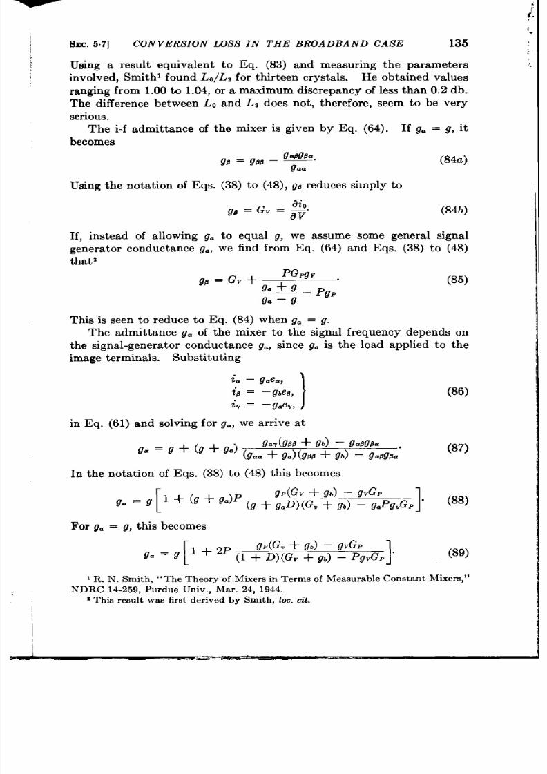
SEC. 5 .7]
CON VERS ION LOSS IN
sing a resu lt equiva len t to Eq.
THE BROADBAND CASE
135
(83)
and measuring the pa ameters
involved, Smithl found Lo/Lz for th ir teen crysta ls. He obta ined values
ranging from 1.00 to 1.04, or a maximum discrepancy of less than 0.2 db.
The cliffer ence between LO and Lz does not , therefore, seem to be very
serious.
The i-f admit tance of the mixer is given by Eq. (64). If g. = g, it
becomes
sing the nota t ion of Eqs. (38) to (48), g8 reduces simply t
(84a)
(84b)
If, instead of a llowing g. to equal g, we assume some genera l signa l
genera tor conductance go, we find from Eq. (64) and Eqs. (38) to (48)
tha t ’
PG@v .
g~=Gv+
9.+9
— – PgP
ga–g
(85)
This is seen to reduce to Eq. (84) when go = g.
The admit tance ga of the mixer to the signal frequency depends on
the signa l- enera tor conductance go, since ga is the load applied to the
ima ge t ermin als. Su bst it ut in g
L = gee=,
i. =
– gbefl,
i~ =
– g.e~,
1
in Eq. (61) and solving for g., we a r r ive a t
9. =9+(9+9.)
fbbd + d – 9.89B.
(9.. + 9.) (9LM+ gb) – gaBgh”
In the nota t ion of Eqs. (38) to (48) th is becomes
[
g,(Gv + gJ – gvG, -
g.=g
1 + (!J+ 9“)P(g + gaD) (Go + gb) – 9.PWGP.
For g. = g, thk becomes
[
gdG. + gb) – gvGp
ga=g
1
‘2P (1 + D)(G. +$%) –pg@, “
(86)
(87)
(88)
(89)
1 R. N. Smit h, “Th e Th eor y of Mixer s in Terms of Mea sur able Const ant Mixer s, ”
NDRC 14-259,P u rdu e Univ., ‘Ma r. 24, 1944.
: Th is r esu lt wa s fir st der ived by Sm it h, 10C.m “t .

136
FREQUENCY CONVERS ION
[SEC.58
5s8. Genera l Expression for Conversion Loss. Min im ization w“th
Respect to the S ignal Load Adm ittance.—In t he pr ecedin g sect ion expr es-
sions were der ived for loss under the rest r ict ing condit ion that the load
admit tances at signal and image frequencies were the same.
These
result s a re now genera lized to find the loss with arbit r ary load admit -
tances.
To make the resu lt s as genera l as possible, no assumpt ions will,
for t he pr esen t, be m ade wit h r ega rd t o r ecipr ocit yy, bu t t he in vest iga tion
will be based on the genera l form of the admit tance mat r ix of a 1ow-Q
m ixer [E q. (6)].
If an admit tance y. loads the image terminals, we have
i; = – y~e~.
(90)
With the aid of Eq. (90) we eliminate i: and et from Eqs. (2) and (6).
This has the effect of reducing the admit tance mat r ix t o a 2-by-2 form,
in which on ly signal and i-f quant it ies appear .
We obt ain
where
Y=. = y.. – YA*,
Y:a + ‘!/.
(91)
(92)
(95)
Equat ion (91) represen t s the two-terminal-pa ir device of Fig. 5.6. The
mixer is dr iven at the signal t er -
+~:m~
r nin als by t he cu rr en t sou rce of pea k
st rength A of in ternal admit tance
y= = g. + jb=. The available power
from the signal genera tor is then
FIG.5.6.—Mixer-terminal conditions for
a rbit ra ry im age loa d con sider ed a s pa rt of
t h e m ixer .
P, = g.
(96)
The i-f admit tance y~ of the mixer is found by suppressing A, with the
result
i. = —ye=. (97)
Subst itu t ing this in Eq. (91) and solving for y8 = iR/eB, we find
(98)

SEC. 58]
GENERAL EXPRESS ION FOR CONVERS ION LOSS
Next , we find the i-f cu r ren t in to a shor t circuit . With
A = em ya + i.,
e~ = 0,
we find for i~
Ypa
iP=A
Y.= + y.”
The available ou tput power is
p, = Iid l’ - & IYA’
8gfl 8gp IY== + y.lz”
The loss is then given by
where y. = g. + jb.. If one pu ts
Y.. = G.. + jB=.,
Ypfl = Gb8 + jB8b,
and
Y.flYp.
u+jv=—
G.=G08‘
137
(99)
(loo)
(101)
(102)
(103)
(104)
Eq. (101) becomes
Y.p (G.. + g.) ‘ – uG..( .. + g.) + (B.. + b.) 2 – VG==(Bam+ E)a)
L=~=
Gmag. ~U2 + V2
(105)
Equat ion (105) gives th e most gen era l expression for con ver sion loss.
All other loss expressions may be der ived from it by specia liza t ion . For
example, taking y. and yC to be equal and rea l, and assuming weak
reciprocity, with the consequence of a rea l 3-by-3 admit tance matr ix, we
obta in from Eq. (105) the expression [Eq. (67)] for loss in the “ broad-
ba nd” ca se.
Equat ion (105) is a conven ien t sta r t ing poin t for an invest iga t ion
of the separa te effects of signal and image load admit tances. Leaving
the image load admit tance fixed a the arbit ra ry va lue y., it is fir st
sh own t ha t L of Eq. (105) has a unique minimum as a funct ion of signal
load admit t ance .
To min im ize L wit h r espect t o t he sign al-loa d a dm it ta nce
IA = g. + A,
we first pu t
aL
K
= o,

138
FREQUENCY CONVER SION
[SEC.5%
which, applied to Eq. (105), gives
If Eq. (106) is
defin ed by
b. =~Ga. –B...
(106)
subst itu ted in Eq. (105), and the symbols x, a, and b
z=k,
G
. .
a=l—~+~~uz+vz,
I
(107)
,6A
b = ~U’ + Vz,
)
Eq. (lo5) t akes the form
L=~(~+a)(z+a–b)
bz “
(108)
The expression involving z her e is see to have the genera l form of
Eq. (68). ccordingly from Eq. (70) we find, for the minimum loss,
(109)
where
The signal load admit t ance giving this minimum loss is found from
Eqs. (69), (107), (104), and (106). It is
With the signal load admit tance [Eq. (11 l)], the i-f admit tance of the
mixer , found by subst itu t ing Eq. (111) in to Eq. (98), is
If an i-f load admit tance yb, equal to the con jugate of yp [Eq. (112)],
is placed across the i-f t erminals, it may be shown from Eq. (91) in the
usual way that the signal admit t ance ~{a of the mi er is the conjugate
of y., as given by Eq. (111). The mixer will then be matched to the
sign al a nd i-f ext er na l cir cu it s.
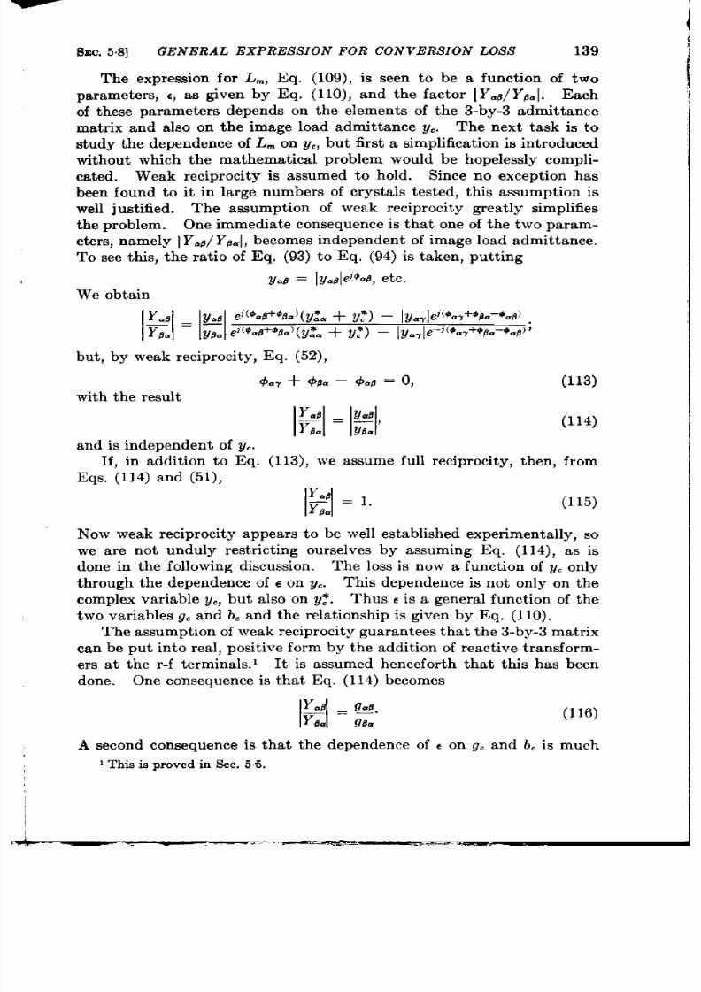
.
SEC. 5 .8]
GENERAL EXPRESS ION FOR CONVERS ION LOSS
139
Th e expression for L~, Eq. (109), is seen to be a funct ion of two
parameters, q as given by Eq. (110), and the factor IY.P/ Y8=I. Each
of these parameters depends on the elemen ts of the 3-by-3 admit tance
matr ix and also on the image load admit tance y..
The next ta sk is to
study the dependence of
L~
on Y., bu t fir st a simplifica tion is in tr odu ced
withou t which the mathemat ica l problem would be hopelessly compli-
ca ted. Weak reciprocity is assumed to hold. Since no except ion has
been found to it in la rge numbers of crysta ls t ested, th is assumpt ion is
well just ified. The assumption of weak reciprocityy grea t ly simplifies
the problem. One immedia te consequence is tha t one of the two param-
et er s, n amely ]Y_8/ YP_1, becomes in dependen t of image loa d adm it ta nce.
To see this, the ra t io of Eq. (93) to Eq. (94) is taken , pu t t ing
but , by weak reciprocity, Eq. (52),
% +
49. – % = 0,
(113)
with t he result
(114)
and is independent of y..
If, in addit ion to Eq. (113), e assume full r eciprocity, then , from
Eqs. (114) and (51),
Y.
l-l
@m
= 1,
(115)
Now weak reciprocity appears to be well established exper imenta lly, so
we are not unduly rest r ict ing ourselves by assuming Eq. (114), as is
don e in t he followin g discu ssion .
The loss is now a funct ion of y. only
throug the dependence of E on y..
Thk dependence is not on ly on the
complex variable y., but a lso on y:.
Thus e is a genera l funct ion of the
two variables g. and b. and the rela t ionship is given by Eq. (110).
T’h e assumption of wea k r ecipr ocit y gu ar an tees t ha t t he 3-by-3 ma tr ix
can be put in to rea l, posit ive for by the addit ion of react ive t ransform-
ers at the r -f terminals. 1 It is assumed hencefor th tha t th is has been
done. One consequence is tha t Eq. (114) becomes
(116)
A second consequence is tha t the dependence of t on g. and b. is m uch
1This ie proved in Sec. 5,5.
140
FREQUENCY CONVER S ION [SEC.
59
less complica ted than in the genera l case. This dependence of t and
the consequent dependence of L~ on image load admit t ance is studied
in t h e following sect ion .
5.9. Effect of the Image Terminat ion on Conversion Loss.—The
convers ion loss L~, minim ized wit h r espect t o t he signa l loa d a dmit ta nce,
is given in consequence of Eqs. (109) and (116) by
where c is given by Eq. (110).
The assumpt ion of a rea l 3-by-3 mat rix (a consequence of weak
reciprocity) simplifies the expression for c to
[(x + 1 – e)’ + #’l[(x + 1)’ + +’]
‘ = “ [(x + 1)(X + 1 – 82) + +21[(X + 1)(X + 1 – Cl) + +’] + w%”
(118)
IJ h er e t her e h ave been in tr odu ced t he a bbr evia tions
(119)
Th e loss L~ depends on image termina t ion y, = g. + jbC t hrough t he
dependence of c on y. and #. This dependence is ra ther complica ted, and
to see how L~ depends on image termina t ion we must first study the
funct iona l dependence
6 =
C(X,*).
We find at once as specia l cases of Eq. (1 18) the values of t for shorfi
cir cu it ed a nd for open -cir cu it ed image t ermin als.
1. Shor t -c r cu it ed image t ermin als.
gc=m
(i.e., either x = m or ~ = m, or both),
, =,1 = -’!.
9..96’B
2. Open-circuited image terminals.
y.=o (i.e., both
(120)
X= Oand~= O),
t l
l–e
~=e3= ————.
1–,,1+0
(121)
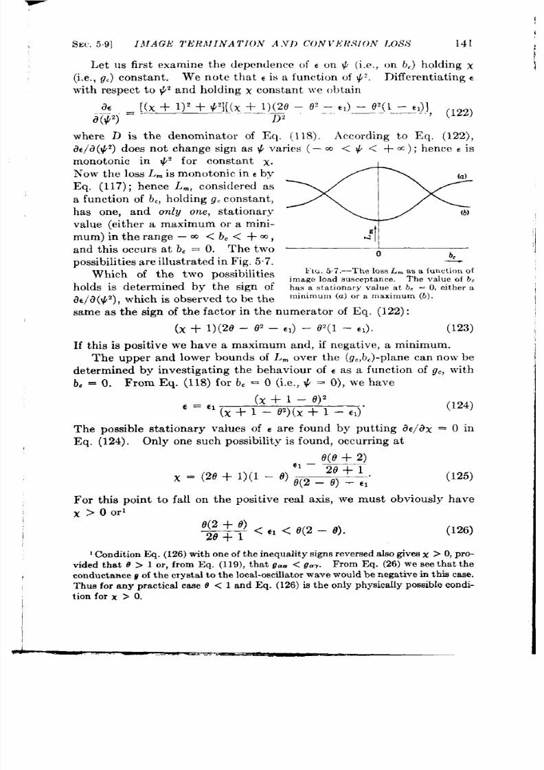
SEC. 59]
Let us
IJ fAG.E l’EItMINA TION A .Vl~ CON VliR .~1 ON 1.OSS
1’41
first examine the dependence of t on & (i.e., on b.) h olding x
(i.e ., g<) constan t . We note that c is a funct ion if ~’. Diffeien t ia t i{g e
with respect t o +2 and holding x constan t we obtain
= [@ + 1)2 + +:I[(X +_})@ – ‘9’ _- ‘1) – 82(1..–-1)I, (122)
a(#2)
~,
wher e D is the denominator of Eq. (118). According to Eq. (122),
a t la (~’) does not change sign as + va r ies ( – ~ < ~ < + ~); hence q is
monotonic in +2 for constan t x.
h ’ow the loss L~ is mon ot on ic in Eby
Eq. (117); hence Z&, considered as
a funct ion of b., hold ing g. con st an t,
has one, and on ly one, stationary
va lue (either a maximum or a mini-
mum) in the range — co < b. < + ~,
and th is occu r s a t b. O. The two
poss ibilit ies a r e illu st r a ted in F ig. 5“7.
Which of the two possibilit ies
holds is det ermined by the sign of
a t /a (t i2), wh ich is observed to be the
4
0
b.
-
l’1~, 57.-Th e loss Lm as a funct ion of
image loa d su scept an ce. Th e va lu e of b.
h as a st at ion ar y va lu e a t b, = O,eit her a
m in imum (a ) or a maximum (b).
sa ’me ‘as ‘the sign of the factor in the numera tor of Eq. (122):
(x + 1)(20 – e’ – c,) – 0’(1 – 6,).
(123)
If th is is posit ive we have a maximum and, if negat ive, a minimum.
The upper and lower bounds of L~ o er the (g., b,)-plane can now be
determined by invest iga t ing the behaviour of c as a funct ion of g., with
b, = O. From Eq. (118) for b. = O (i.e., # = O), we have
(X+l– e)’
‘= ’’(X+ 1–02)(X+1– CJ ’
(124)
The possible st a t ionary va lues of E a re found by put t ing &/dx = O in
Eq. (124). Only one such possibility is found, occu r r ing a t
0(0 + 2)
“- 2/3+1
~ = (20 + 1)(1 – O) 0(2 _ @ _ ,,”
(125)
For th is poin t t o fa ll on the posit ive rea l axis, we must obviously have
X> Oor l
e(2 + e)
~o+l <,, <0(2– 0).
(126)
! Con dit ion E q. (126) wit h on e of t he in equ alit y sign s r ever sed a lso gives x > 0, pr o-
vided that 8 > 1 or , from Eq. (119), that gu= < guw
From Eq. (26) we see that the
con du ct an ce # of t h e cr yst al t o t h e loca l-oscilla tor wa ve wou ld be n ega tive in t his ca se.
Th us for a ny pr act ical case o <1 a nd Eq. (126) is t he on ly physically possible con di-
tion for x >0.

1
,
142
FREQUENCY CONVERS ION [S EC.5.9
The poin t given by Eq. (125) must a lways correspond o a minimum in
c (i.e., a maximum in L~), as can be ver ified by examining he secon
der iva t ive of Eq. (124). Fur ther , if th e su rface L.,(g.,b.) is con sidered,
themaximum along therea laxis(h = O) must a lso beamaximum in the
or th ogon al dir ect ion (g. = con st an t).1
The proof follows from the fa t
tha t , when Xis given by Eq. (125), Expression (123) is a lways posit ive;
hence we have Condit ion b of Fig. 5“7. Since th is maximum in L~, when
it exist s [i.e., when Eq. (126) is sa t isf ed], is the only sta t iona ry va lue of
L~ over the (g., b.)-plane, it is an upper bound on L~. When the maxi-
mum does not exist , L~ is bounded by its va lues a t YC= O and y. = m.
In an case, the lower bound for L~ is th e les er of it s va lues a t y. = O
‘w”
FIG. 5.S .—The (CI - q)-p lane.
andy, = ~.
The va lue of c a t th e maximum
for L~ will be ca lled c,, and the
cor respondin g maximum loss, L~.
Subst itu t ing Eq. (125) in to Eq.
(124), we fin d
It is easy to ver ify from Eq. (127)
tha t e~ < c, and c, < c~. We can
t r an sla te t he con dit ion in Eq. (126)
for existence of the maximum loss
in to rela t ions between ~1and Cj by
use of Eq. (121). Thus we find
that the maximum loss Li exist s when the following two condit ions a re
satisfied:
t3 < f(fl), (128)
61 < j(63),
(129)
where
(
j(z)=* 1+<*
)
—— .
(130)
By Eqs. ( 20) and (121) these condit ions on c1 and ESare condit ions
When the matr ix for any crysta l is known, the value of c, and t t can
be found from Eqs. (120) and (121). The crysta l can then be represen ted
as a poin t on th e (cl,~3)-plane. Th is plane can be par t it ioned in to region s
by the curves c1 = f(cs), CS= j(c,), and c1 = c,, as is shown in Fig. 5“8
(wher e the line o = O or c, = c,/1 – c, has a lso been drawn). It is not
possible for a crysta l poin t to fa ll in Region 5, since such a crysta l wou ld
have a nega t ive value of o which is excluded by defin it ion (see Sec. 5“5)
1Tha t is , the re is never a sadd le poin t .
I
SEC.59]
IMAGE
of the standard r-f
TERMZNA TION AND CONVERS ION LOSS
143
terminal posit ion. If a point fa lls in Regions 2 o 3,
t he maximum L, exist s; if in”1 or 4, Ld does-not exist and L: is bounded
by L, and La (cor responding t o c1 and e,, tha t is, to shor t -circuit ed and
open -cir cu it ed im age t ermina ls, r espect ively). If a point falls in Region s
1 or 2, La < Ll and, if in 3 or 4, L1 < La. If a point fa lls on el = C3
then of course L1 = La and it may also easily be shown that Le = Lb;
tha t is, if
L1 = L~, the
maximum loss
L4
occurs when the image termina -
t ion is the same as the signal t ermina t ion . A point fa lling on CS = f(cl)
has
LI = L4 and a point fa lling on c, = j(t~) has L, = L,. The forms
of t he surfaces L~(gC,bC)cor responding t o t he four regions, as well as t he
specia l case c1 = cS, are shown in Figs. 5.9 a, b, c, d, and e.
The expr ession for L, obta ined by subst itu t ing Eq. (127) in Eq. (1 17)
can be simplified t o
(131)
If Eq. (121) is solved for 0 in terms of c1 a nd c~, t he above result becomes
L,=2
If LO [E q. (77)] is wr it ten simila rly in t erms of c1 and c3,we obt ain
‘ 0 = 2 %( : + : - ’ )
From qs. (132) and (133),
1
L4=L, -——
()
2<
1– ~–~
61 63
N w l/c1 — l/CS cannot become la rger than ~
of Fig. 5.8 (wher e L, exists). Consequent ly,
(132)
(133)
(134)
in the Regions 2 and 3
(135)
or , L, never exceeds Lo by more than 0.5 db.
From Eq. (73) we find for q! in terms of c1 and cS,
72 = 61 + C3— 6163. (136)
Thus, from Eq. (72),
L2=290@1+d
(1 – 6,)(1 – 63),
98.1 – /(1 – C,)(l – 63)
(137)
#
1,
.,
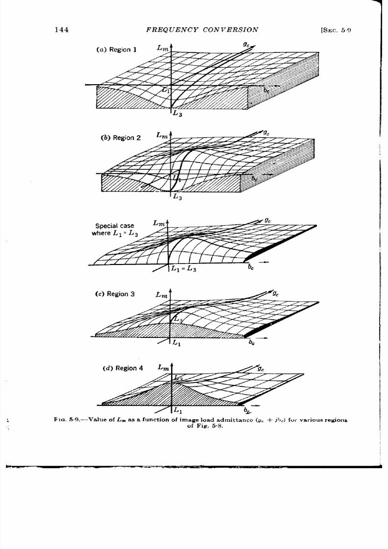
144
FREQUENCY CONVERS ION
[SEC,59
//
9C
whereLI =L3
F1~.5.9.-Va lue of L~mafunct ion ofimage load admit t ance (g. +~$.) forva r iou sr eu ion fi
of F ig. 5.S.
—
1
I
SEC,5.9]
IMAGE TERMINATION AND CONVERS ION LOSS
145
and it may be shown that
(138)
It can easily be shown that LO may be writ t en in either of the two
forms, Eq. (72) or Eq. (117), provided we replace m and c by ~0 a nd co,
where
4ele3
‘“ = (,, + ,,)’~”
(139a)
8e,e392
‘0 = (,1 + ,, + q,)’”
(139b)
Furthermore, L, may also be writ ten in these forms by put t ing
Th e la tter equ at ion is, of cou rse, just Eq. (127) expr essed symmetr ica lly
in terms of c1 and o
To recapitu la te, th ere have been defined the following los es (see
Table 5.1).
Lo (mixer ma tched to loca l oscilla tor , same termina t ion a t signa l and
image fr equencies )
L, (m ixer m at ch ed t o sign al, im age sh or t-cir cu it ed a t r -f t ermin als)
Lz (minimum loss with same termina tion at signal nd ima ge frequ en-
cies)
Ls (m ixer mat ched t o signal, ima ge open -circuited at r -f terminals)
L4 (mixer matched to signal, image impedance adjusted to give max-
imum loss ~vhen this ccurs a t other than open-cir cu it ed or shor t -
cir cu it ed image)
The r-f terminals have been so chosen tha t the mixer matr ix element s
a re all rea l and posit ive. The five defined quan tit ies a re then given by
()
,=@ l+t il-t i
1
..!78. 1 – <1 – q’
~=o, l,3,4,
where co is given by Eq. (139 b), c1 by Eq. (120), CSby Eq. (121) and
C4by either Eq. (127) or Eq. (140 b); and/or by
(9)
,=2gal+v’1-lli ,:
1
= o, 2, 4,
Pa l—~l—~j’ “
(142)
i
;
146
where vo is given by
FREQUENCY CONVER SION
[SEC.5.9
Eq. (139a), q2by Eq. (73) orEq. (136), and7, by
Eq. (140cz). - The quant it ie Loand L, may reexpressed more direct ly
in terms of measurable quant it ies by Eqs. (77), (78), (79), and (133) in
the case of LO, and byEq. (131) in the case of Li. All of the character -
ist ic loss va lues LO-L4 are then completely determined, except for the
constant reciprocity factor g.O/go., by two character ist ic funct ions t l and
t~of themixer ma tr ix elements. Rela t ions among th se losses are given
by Eqs. (77), (141), and (145).
o see how the values of the character ist ic losses run for actua l
crysta l rect ifiers, computa t ions have been made for six silicon and seven
germanium unit s. The resu lt s a r e given in Table 5.2. The fir st column
gives the ident ifica t ion ; in Columns 2 to 6 are the da ta obta ined for these
units a t the 10-cm band by Smith. 1 The quant it ies in Columns 2 to 6
are defined by Eqs. (26) and (37). The complete mixer ma tr ix may be
obta ined from these quantit ies through Eqs. (38) to (48). (Through
proper choice of r -f termina ls b = bv = b, = O.) The values of @, cl,
and CSwere then computed from these data and are given in the next
th ree columns. The five losses were next computed; they a re given in
Columns 10 to 14. The quant ity Li is given herever it exists. In
Column 15 is given the ra t io of the image conductance for maximum
1ass Li to the local-oscilla tor conductance of the mixer . Finally, in
Column 16 the quant ity ga8 gB., w ich is a factor in all expressions for
loss [E qs. (141), (142)], is given in decibels.
Any loss equa t ion can be writ ten
(143)
As wi l be shown la ter (see Sec. 7.3), the quant ity
L;,
the so-ca lled
(‘impedan ce loss, ”
may be determined by impedance measuremen ts a t
either the r -f or i-f terminals of the mixer , whereas it is impossible to
det ermin e g.~/gB. in th is m an ner .
We can find L; from the table by sub-
t ract ing Column 16 from Columns 10 to 14. The depar tu re of g~~/g@~
from unity measures the exten t of fa ilure of fu ll reciproc ty. In fact ,
the crysta ls of Table’ 5.2 a re the same as those represen ted in Fig. 5.4,
used to test reciprocity. It will be recalled tha t , on plot t ing IV.BIUS.ypal
m Fig. 5.4, it was found that the best st ra igh t line fit t ing all crysta ls
except G40, 111, and llN did not have a slope of exact ly 45”, and it was
ment ioned that th is cou ld perhaps be a t tr ibuted to a s stemat ic er ror
in the measurement of r -f power . Such an er ror will accoun t for the
predominance of negat ive signs in Column 16. Thk possibility was not
taken in to acc un in comput ing the losses of Ta le 5.2; had it been
?
I The a uthors a re indebted to Dr . R. N. Smith for h is indness in furn ish ing t heee
data .

-
TABLE5.2.—DATAONTHECONVEIWIONROPE 14TIESF A NUMSEEtOF SILICONANDGEIMANIUMECTIFIEIW
s
1
Crystal
L114 Si
L104 Si
K900 Si
BRD3 Si
BRD2 Si
M97 Si
G129 Ge
G236 Ge
G40 Ge
13V Ge
111 Ge
lIQ Ge
llN Ge
2
P,
mw
0.41
0.27
0,47
0.58
0.66
0.68
0.64
0.38
0.39
0.30
0.49
0.59
0.87
3
GP ,
volt-]
1.43
1.89
1.39
1.10
1,13
0.55
1.45
1.44
1.72
1.31
1.00
0.38
4
Gv,
rOlt–
2.46
3,6
2.5
2.17
2.2
1.23
1.16
2.55
4.0
3.3
4.0
2.0s
1.9
5
Gp ,
row-i
0.69
1.39
0.72
0.43
0.425
0.46
0.54
1.70
1.85
1.74
1,30
0.40
0.31
6
Gv,
m ho
4.00 x 10-’
1.73
1.90
2.40
3.05
0,65
1.37
1.40
1.49
1,90
0.2
0,71
7
e
0.2%?
0.376
0.338
0.249
0.281
0.346
0.646
0.722
0.522
0.637
0.236
0.270
89
*1
e3
0.334 0.280
0.630 0.771
0.565 0.64Li
0.435
0.463
0.433 0.428
0.169
0.490 0.466
0.744 0.625
0.852 0.931
0.70s 0.755
0.789 0.805
0.136 0.0974
0.548 0.69
10
L, ,
db
9.8
5,55
6.2
8.35
8.6
11.9
8,3
5.4
5.4
5.3
6.6
15.4
10.6
11
L, ,
db
9.3
5.9
6.4
8.4
8.4
11.0
8.0
4.3
4.9
5.1
6.1
14.6
11.1
12 13
L, ,
db
9.7:
5.4
6.1
8.3:
8.6
11.8
8.3
5.2
5.3
5.2
6.6
15.3
10.4
L,,
db
10.2
4.3
5.5
8.0
8.5
12.8
8.3
5.6
3.8
4.5
5.9
16.1
9,4
14 ~ 15 16
—l—,—
L, ,
I
~ lg \ 9dga-,
db L
db
. ..1.-I –065
. ..l . . ..~-o.2
. . . . .
–0.5
8,41 . . .. ’–0.1
8.6
0.71
8.3
0.21
. .
5.4 1.7
5.3 2.1
6.6 1.5
. . .
. . .
–0.1
–0.6
+0.2
–0.6
+1.4
–0.2
+1.8
+0.2
+4.0
2
b

148
FriWQuENcl’ CONVERSION
[SEC.510
done, the va lues for the losses would have been slight ly increased ( = 0.2
db) but their rela tive va lues wo ld not have been significant ly a ltered.
A cr yst al m ixer is som et im es u sed as a modula tor , in }vh ich a lo~v-level
signal at a frequency low compared with microwave frequencies is
impressed on the i-f termina ls of ‘the mixer .
By bea t ing with a micro-
wave local oscilla tor a t high level ( =
I mw) this low-frequency signa l is
conver t ed to sidebands of the loca l oscilla tor . The conversion loss to
either sideband can be shown to be given by
( )
: @i,
j=l) 2)3,4. (144)
Now all significant depar tures of gaB/gP=from unity observed so far are
such tha t geP > gfl.. Thus, for cer ta in (germanium) units it is possible
[from Eq. (144)] to obta in a very 10IVloss from i-f to signal. For exa ,m-
ple, units G40, 111, and 1lN have values of L; equal, respect ively, to
1.0, 2.3, and 1.4 db, whereas the cor responding values of LS a re 3.8, 5.9,
and 9.4 db. Such effects do not appear to occur in silicon ect ifier s.
It will be seen from Table 5.2 tha t Lo and L, do not differ by more
than 0.2 db for any crysta l; tha t LA, }vhen it exists, is pract ically the same
as LO; tha t the varia t ion in loss amounts to O to 1.8 db over the image-
admit tance plane; and tha t la rge var ia t ions in loss as a funct ion of
image admit tance occur about as often for poor crysta ls as for very good
ones.
The same crystals of Table 5.2 are plot ted on an (c,,c~)-diagram in
Fig. 5.10. The germanium units a re represented by encir cled crosses,
and the silicons by circles. It is in terest ing, but perhaps not significant ,
tha t the silicon points fall very near ly on a stra ight line, while the
germanium poin ts a re con sider ably sca tt er ed.
6.10. Effect of I age Termina t ion on I-f Impedance.-The i-f
impedance of the mixer is a quant ity of considerable impor tance in
receiver design. The noise figure of the receiver is determined by the
conversio loss, the noise tempera tur e of the crysta l, and the noise figure
of the i-f amplifier . It has a lready been noted (Sec. 2.5) tha t conver~lon
loss and crysta l noise tempera ture depend on the r -f load admit tance
of the mixer .
Similar ly, the amplifier noise figure depends on the i-f
im peda nce of t he m ixer .
In designing an amplifier of low noise figure, some definite va lue of
mixer impedance must be chosen.
It is impor tant , once this va lue has
been set , tha t we be able to rely on the mixer impedance not to v ry
much from one crysta l to another or from one mixer to another . In
pract ice it is found-that the i-f impedance of crysta ls made by one manu-

SEC.5.10]
IMAGE TERMINATION AND I-F IMPEDANCE
149
factu rer a re reasonably uniform in the same mixer , but tha t differences
occu r between pr odu ct s of t wo man ufa ct ur er s.
Su ch differ en ces a re n ot
ver y gr ea t and can be cor rect ed by specifica t ion limits on i-f impedance.
More ser ious, however , a re var iat ions in i-f impedance for the same
crysta l from one mixer t o another .
Such var iat ions a re caused pr in-
cipally by the fact tha t the terminat ions to the image frequency differ
in different mixer de igns. Thus, if mixer A happen s t o shor t -cir cu it
1.C
0.s
0.8
0.7
0.6
w- 0.5
0.4
0.3
0.2
0.1
0
-o
()
’,, # LI
in db
15.5 12.6 10.59,79,0 8?7.6 7.16.55.95354.84.2 .5 2,8 2.0 0
I
1
I
I
I
I
(5)
- 6.5
v
4 7.1 .s
- 7.6 Q
+’
8,3 -~
- 9.0 -j’
- 9.7
- 10.5
- 12.6
- 15.5
1
I
I
I I
5
0.1
0.2
0.3
0.4 0.5 06 0.7
0.8 0.9 10
(
,
,
(4)
‘f,
FIG.5.10.—P lot of t he cr yst als of Ta ble 52 a s poin ts on a (CI, q) dia gr am (see F ig. 5.8).
t he image, and mixer B
to open-cir cu it t he image, the i-f impedances
of the same crysta l in the t !vo mixers ivill be very differen t ; the t ivo values
of i-f impedance may be in a ra t io of as much as 3 or 4 in the case of a
low-loss crystal. Var iat ions of th is magn itude actua lly occur and arc
very ser ious fr om the poin t of view of receiver noise figu re.
The effect of var ia t ion of image load impedance on i-f impedance
must depend, obviously, on the conversion loss of the mixer .
F or low
loss crysta ls there is only a small decoupling between the r -f circuit and
.
150
FREQUENCY CONVER S ION
[SEC.5.10
the i-f circuit and we must expect such effects to be severe. Var ia t ions in
sign al loa d a dm it ta nce a re of cou rse equa lly effect ive in pr odu cin g va ria -
t ions in i-f impedance but are unimpor tant in pract ice, since mixers are
uniformly designed to match the signal.
The rela t ion between con-
version loss and terminal impedance has been u tilized in actua l loss
measure ents, as will be descr ibed in Sec. 7.3.
As an example of the dependence of i-f impedance on image termina-
t ions, the i-f impedances of t e th ir teen crysta ls of Table 5.2 will now be
calcula ted for (a) image terminals shor t -circu ited, (b) image terminals
open -cir cu it ed, an d (c) t he ca se of equ al sign al an d im age loa d a dmit ta nce
adjusted to equal the loca l-oscilla tor admit tance g of the mixer .
It is
assumed tha t in Cases (a) and (b) a lso the signal load admit tance is g.
Let the i-f admit tance of the mixer be y8, and the image load admit -
tance be y.. The terminal cur ren ts and voltages a re then rela t ed by
Subst itu t ing Eqs. (145) in Eqs. (2) and (13) and eliminat ing the
cu rrent s and voltages, we obta in
r
a
+9.$
9.7
9e .
968 – Y+Q90.
= o.
9.7
9.@
9.. – y:
Solving for y~, we arr ive a t
9.698.(39 + Y:)
‘o = ‘ g(3gm=
– 9) + Y.(9.. + 9)
= g b –
9.898.
g.. +
kg’
where
k–ye–g,
y. + 39
(146)
(147)
From Eqs. (146) and (147) we get for the th ree specia l cases:
(a)
u.=
~1
(image short-circui ted)
1
9P=9PP–=-=—;
g.. + g R,
(b)
y. =
o,
(image open -cir cu it ed )
9@=98#–= ’~;
R,
g.. – g
I
(148)
(c)
y, = g,
(in t ermed ia t e ca se)
9@=96@-g~=~.
)

SEC.5.10]
IMAGE TERMINATION AND I-F IMPEDANCE
151
Tocalcula tethe i-f impedances of the crysta ls of Table 5.2, we sub-
st it ut e for g.a et c., t heir va lu es in t erms of mea su ra ble. m ixer pa ramet er s,
as given by Eqs. (38) to (48), obta in ing
(149)
The th ree specia l cases (a), (b), and (c) are then given by let t ing
k
equal,
respect ively, 1, —~, and O.
TABLE5.3.—I-F RESISTANCEFA~U~BEROFCRYSTALSORIMACESHORT-CIRCUITED
(It,), MATCHED1?,), ANDOPEN-ClRCUITEII
R,)
Crys ta l No.
R,, ohms
I
L114
L104
K900
BRD3
BRD2
M97
G129
G236
G40
13V
111
llQ
llN
207
347
313
250
320
1100
415
316
380
265
92
930
R,, ohms
250
530
420
330
370
1540
730
710
670
530
98
1410
R,, ohms
297
764
830
560
430
415
2100
1350
1750
1230
1080
104
2300
It is eviden t tha t Ra = l/g~ is smallest when the image is shor t -
.
circuited, and largest when the image is open-circu ited. -
The values of
Rl, R*,
and
RS
of Eqs. (148), as computed from
the data of Table 52 for the 13
reference crysta ls, a re given in
Ta ble 5.3.
The case of a genera l r eact ive
im age t erm in at ion follows ea sily
fr om th e specia l ca ses con sider ed.
Since the mixer acts as a linear
n et wor k con nect in g t he im age cir -
cu it to the i-f circu it , it is clea r
tha t y~ t raverses a circle in the
yrplane as he l ne between the
mixer and a fixed image termina-
t ion is “st retched.” The circle
will be a circle of “constant r e-
flect ion coefficien t” wit h r espect
This cir cle is shown in Fig. 5.11.
FIG. 5.11.—Circle diagram on the i-f
a dmit tance plane. For a gener al react ive
image t ermin at ion , t he i-f a dm it ta nce fa lls
cm t he cir cle whose in ter cept s a re l/ R s and
l/RI as given by Eq. (14S).
to the conductance go = l / ~RlR3.

152 FREQUENCY CONVER SION
[SEC.510
If a resonan t cavity (TR switch ) tunes the r -f circu it , t he signal will,
in genera l, see a nea r match (for example, g) bu t th e image will see an
admit tance determined by the loaded of the cavity and the line length
from the cavity t o the reference terminals of the mixer . As th is line
length is va r ied, the i-f admit tance will t raver se a circle for which the
in tercept s on the rea l axis will be given by Eq. (146), wi h
(150)
where f and A~ are the local-oscilla tor and in termedia te frequencies,
r espect ively, and Q is the loaded Q of the TR switch . As an example, if
f = 3000 Me/see,
Aj = 30 iYfc/see,
Q = 300,
then the values k = +0.90 and k = –0.32 give th e in tercepts. This is to
be compared with
k = 1
and
k = –+
for Q = m . Thus in actual prac-
t ice the image tuning has an impor tant effect on the i-f impedance.
TH PHYSICAL THEORY OF CONVERSION
The theory of conver sion , as developed to th is poin t , is phenomeno-
logical in tha t th e proper t ies of the mixer a re der ived from measurements
a t it s termina ls and no assumptions a re made as to the in terna l st ructu re
of the device. This theory gives a ll the informat ion requ ired by the
system design er but is in su fficient t o a id in t he developm en t an d im pr ove-
men t of cry ta l rect ifier s. A differen t viewpoin t will be adopted now
,8
and the theory of mixers will be based on the
I
physica l proper t ies of crysta l rect ifiers by a con-
sidera t ion of, fir st , t he ixing act ion of a simple
t ,
c
n on lin ea r r esist an ce, a nd secon d, of t he modifica -
FIG. 5.12.—Equiva-
t ion of th is act ion by the addit ion of impedance
lent circuit of a crysta l
elemen ts connect ing the non linea r resistance t o
rectifier.
th e terminals of the actua l mixer . La ter there
will be con sider ed m odifica t ions of th ese resu lt s ca used by th e n on lin ea r
ca pa cit an ce of t he ba rr ier .
Some of these impedances, such as the bar r ier capacit ance and the
sprea din g resist an ce of th e sem icon du ct or , a re in tr insic proper ties of t he
rect ifier ; others a re in t roduced by the mixer designer as t ransformers
from the ca r t r idge to the mixer terminals. The la t ter type of impedance
is, of cou rse, a lways designed to be purely react ive.
Let us consider
for the moment impedances of the first type.
Th e equ iva len t circu it of a crysta l r ect ifier is r epr esen ted in Fig. 5.12.
I
I
I
I
I
I
I
I
SEC.5.11] MATRIX OF A NONLINEAR RES IS TANCE
153
In addit ion t o th e ba rr ier ca pacita nce C t her e a re ot her r eact ive elemen ts.
Un like C, these a re either negligible or may be tuned ou t externa lly.
This equiva len t cir cu it was discussed in Chap. 2, where it was noted tha t
C is not a t rue capacitance but probably depends on the frequency as
well as on the volt age across it .
At a fixed frequency, however , a close
en ough a pproximat ion t o actua lity can for most pu rposes be a rr ived a t by
assuming the circu it of Fig. 5.12 with C having some average value. In
Fig. 5.12, B is the non linea r r esistance of the bar r ier , C is the b r r ier
capacitance, and r is the spreading resistance of the semiconductor and
may include other losses in the a r t r idge, such as whisker resist ance.
Except in unusual circumstances these a re small in compar ison with the
spreading resis tance .
5.11. Matr ix of a Nonlinea r Resistance.-In consider ing the mixing
a ct ion of a n onlinear resista nce, let t he cur ren t -volta ge cha ra ct er ist ic be
given by
i = j(e).
(151)
The cur ren t and volt age a re assumed to be composed of the following
parts :
(a ) i,
eO
d-c
(t )) ~ im e~n”’ ~ e.ej”o’ LO an d its harmonics
(c) ;e ~ ipe’b~’ ;e ~ e.e’bd
signa l, image, i-f, and harmonic
P
sidebands.
(152)
In (b), the summat ions extend over a ll in t eger va lues of 7~from – CCI
t o + m, not including O. In (c), bp includes the frequencies o + @
(signa l), – @ (image), ~(i-f), and rm + P (harmon ic sidebands).
It is now assumed tha t the t erms in (c) a re very small compared
with the t erms in @) and
(a),
and can be considered, as before, t o be
va r ia t ions of them. The genera l var ia t iona l equat ion i then
*i=@6e
de ‘
(153)
where ~i and ~e a re now iden t ified with the cu rren t and voltage t erms in
Eq. ( 52). For
di/ de, we
may use a Four ier expansion ;
Equa t ion (153) has
by subst itut ion of Eqs.
linear r ela tion s amon g
Lhe cha ract er of a
‘‘ma thema tica l m ixer ,”
since,
(151), (152), and (1 4) in to Eq, (153), we obta in
the coefficien ts of the var ious fr equency corn .

154
ponents. These
e~bdfor t h e same
FREQUENCY CONVERS ION [SEC.5.11
lin ea r r ela tion s a re obt ain ed by equ at in g coefficien ts of
b.. In th is way, we find
+.
ib+w =
z
Yn—.,efl+mu.
~=—.
These equat ions may be writ ten in ma tr ix form
—
. . .
. . .
yo yl yz y3
y4””
,..
y–l o !/1 Y2 113””
y–z y–l yo yl y? “
y–3 y–2 y_l yo
?J1 .
V–4
y_3
Y–2
y–, y,
,..
.
\
. . . . .
Since d i/ d e is rea l, we must have
y–n = y;;
(155)
(156)
(157)
the admit tance matr ix is Hermit ian .
The matr ix will be symmetr ica l
(i.e., r eciprocity holds) if a lso y-~ = y., but th is implies, with Eq. (157),
tha t all y. a re rea l.
It may be shown tha t Y. will be rea l if, and on ly if, di/de is an even
funct ion of the t ime, which implies tha t e is an even fu ct ion of t ime. If
r ecipr ocit y h olds in t he a dm it ta nce m at rix of t he ba rr ier la yer [Eq. (156)],
it will a lso hold for the fina l admit tance matr ix of the mixer .
Thus, a
necessa ry condit ion for reciprocity is tha t a t ime zero can be found such
that e, the voltage across the ba rr ier layer , is an even funct ion of the
t ime. This agrees with one of Dicke’s cond t ions for reciprocityy (see
Sec. 5 .5).
If, followin g t he discu ssion at th e beginn ing of th k ch apter , harm onic
sideband voltages a re neglected and Eq. (157) made use of, Eq. (156)
r edu ces t o
where
Il=lwlll’
(158)
(159)
I
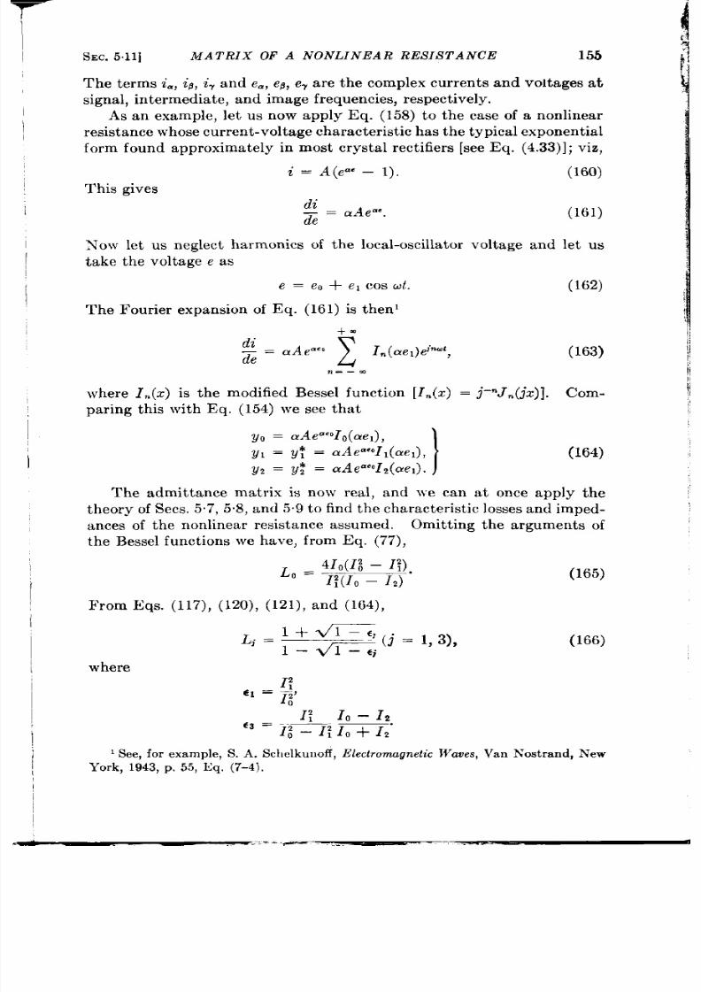
SEC.5.11]
MATRIX OF A NONLINEAR RES IS TANCE
155
The terms i., id, i, and e., eP ,ey are the complex currents and voltages at
signal, in t ermedia t e, and image fr equencies, r espect ively.
As an example, let us now apply Eq. (158) to the case of a nonlinear
r es ist ance whose cu r ren t -volt age cha ra ct er is tic ha s t h e t ypica l exponen t ia l
form fou nd a ppr oxima tely in most cr yst al r ect ifiers [see E q. (4.33)]; viz,
~ = A (e..
– 1),
Th is gives
g=
de
aAe”e.
STOWlet us neglect ha rmon ics of t h e loca l-oscilla t or
take the voltage e as
e = e. + el cos
d.
The Four ier expansion of Eq. (161) is then’
(160)
(161)
voltage and let us
(162)
(163)
where In(z) is the modified Bessel funct ion [I.(z) = j–n .J m(jz)]. Com-
par ing this with Eq. (154) we see that
y, = aAeaeolO(ae,),
yl = y; = aAeaeO1l(aeJ ,
)
(164)
y = y; =
aAe”eO1,(ae,).
The admit tance matr ix is now real, and we can at once apply the
t h or y of Sees. 57, 5“8, and 59 t o fin d t he ch ar acter ist ic losses a nd imped-
a nces of t he n on lin ear resista nce assumed.
Omit t ing the arguments of
the Bessel funct ions we have, from Eq. (77),
410(1; – 1;)4
‘0 = l;(10 – z,)
F rom Eqs. (117), (120), (121), and (164),
~.=l m .
1
1- <’j “ = “ 3)’
(165)
(166)
1See, for example,S. A. Schclkun off,L’Lectromagneticaves,Van Nostra nd,New
York, 1943, p. 55, Eq. (7-4).

156
Also, fr om Eqs. (72),
where
and, from Eqs. (131)
FREQUENCY CONVERS ION
[SEC.5.11
(73), a nd (164),
1+<1–~,
L,=2 —
l–<1–q2’
(167)
21;
‘1’ ‘l.(lO+l,);
and (164),
(168)
It will be reca lled that LO is the loss when the mixer is matched to the
local osci llator; L, and L, are the minimum losses (as a funct ion of the
sign a l-gen er a tor a dm it t an ce) for shor t -cir cu it ed and open -cir cu it ed image
terminals, r espect ively; Lz is t he minimum “ broadband loss” (mixer
t erminated in the same dmit t ance at sign l and image frequencies and
this admit t ance ch osen t o minimize t he loss); and Ld is t he loss minim ized
with respect t o the signa l-genera tor admit tance and maximized with
respect to the image admit tance (see Table 5.1, Sec. 5.6).
It is in terest ing to note that for the simple exponent ia l case the loss
is independen t of the d-c bias volt age eOand of the coefficient A in Eq.
(160). This will not , of course, be t r ue for the mixer impedances. In
the case of actual crysta l rect ifier s, conversion loss does depend on d-c
bias, but the dependence is weak for small bias ( = 0.2 volt ).
Equat ion (160) gives a fa ir repr esen ta t ion of the low-frequency
cur ren t -volt age character ist ic of the bar r ier layer of an actual crysta l
r ect ifier (as point ed ou t in Sec. 4.4).
We saw, however , in Sec. 2.4 that
t her e ar e ot her impeda nce element s inseparably associa ted with a cr yst al
rectifier.
One of these is the capacitance of the barr ier , which will
modify conversion at high frequencies.
This capacit ance cannot be
tuned ou t because of the ser ies ohmic spreading resist ance of the semi-
conductor.
be neglected, and so Eq. (160) gives the cur rent -volt age rel t ionship
of t he r ect ifier if t he spr ea din g r esist an ce is su fficien tly low.
Alt hough Eq. (160) does n ot r epr esen t t he r ever se cha ract er ist ic well,
it may st ill be u sed with confiden ce since, a t h igh frequ encies, t he r ever se
ba r rier r esist a nce is effect ively shor t -cir cu it ed by t h e ba r rier capa cit a nce;
and, in any case, the precise form of the r ever se character ist ic is unim-
por tan t , provided only that the rever se resist ance is high (i.e., gr ea t er
th n 5000 ohms)—a con dit ion sat isfied by m ost cr ysta ls.
In F ig. 5.13,
L1, Lz, and L? have been plot t ed, as calcula ted from
Eqs. (16$168) as funct ions of ael. There have been omit t ed Lo and L~,
since they differ insignificant ly fr om L2 in this case.
The plot may be
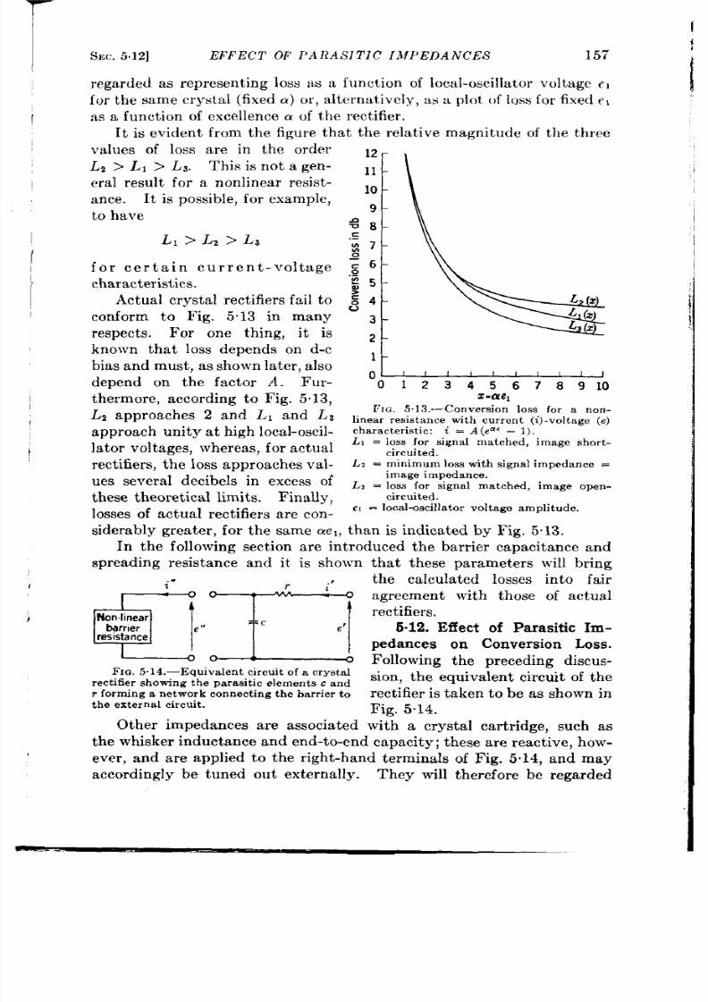
-
}
SEC.5.12]
EFFECT OF PARAS IT IC IMPEDANCES
157
r egarded as represent ing loss as a funct ion of loca l-oscilla tor volt age e]
for the same crysta l (fixed a) or , a ltern at ively, as a plot of loss for fixede,
as a funct ion of excellence a of the rect ifier .
It is eviden t from the figu re tha t the rela t ive magnitude of the th ree
values o loss a re in the order
12-
Lz > L, > La. This is not a gen - ~1
era l resu lt for a nonlinear resist -
10 -
ante . It is possible, for example, ~
t o ha ve
n
=8
L,> L,>LS
c
—
%
7 -
g
for cer ta in cu r ren t -voltage g 6
-
.-
characteristics.
25
g
Actua l crysta l r ect ifiers fail t o g 4
-
v
conform to Fig. 5.13 in many
3 -
respects. For one th ing, it is z
-
known tha t loss depends on d-c
bias and must , as shown la ter , a lso ~
,
t 1 1
I
1 1
1 )
I
depend on the factor A. Fur-
012345678910
t her more, accordin g t o Fig. 5.13,
z.ael
Flc. 5.13.—C0nver si0n 10ss for a n cm -
LZ approaches 2 and LI and L3 linea r r es is t ance with cu r r en t (i)-volt age (e )
a ppr oa ch unit y a t h igh loca l-oscil-
character ist ic:i = A (eae —1).
la ter volt ages, wh er ea s, for a ct ual
L, = loss for sign al m at ch ed, im age sh or t-
circuited,
r ect ifier s, t he loss a ppr oa ch es va l-
L* = min imum los s with s igna l impedance =
. .
image impedance.
u es sever al decibels In excess of LJ = lo~~for ~ign al~.a t~h ~d,ima ge Ope~-
t hese th eoret ica l limits. Fina lly,
circuited.
losses of actua l rect ifier s ar e con-
e, = Iocal-oscillator voltage amplitude.
siderably grea t er , for the same ael, than is indica t ed by Fig. 5.13.
In the following sect ion a re in t roduced the bar r ier capacitance and
spreading resistance and it is shown tha t these pa rameters will br ing
the ca lcu la t ed losses in to fa ir
[r -~ ;ZSEW,,.:3:F,:,
agreemen t with those of actua l
Following the preceding discus-
FIC.5 ,14.—Equiva len t circu it of a crys ta l
rect i fie r showing the paras it ic e lements c and
sion , the equiva len t circu it of the
r forming a network connect ing the bar r ier t o
r ect ifier is t aken to be as hown in
the exte rna l circu it .
F ig. 5.14.
Other impedances are associa ed with a crysta l ca r t r idge, such as
t he whisker inductance and en d-to-en d capa city; t hese ar e r ea ct ive, h ow-
ever , and a re applied to the r igh t -hand terminals of Fig. 5.14, and may
accordingly be tuned ou t externa lly. They will t h erefore be rega rded
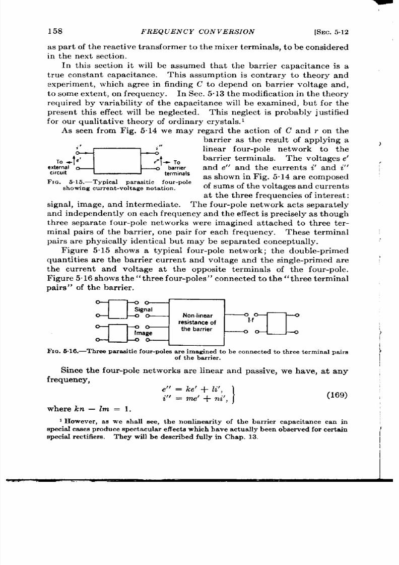
158
FREQUENCY CONVER S ION
[SEC.5.12
as pa rt of t he rea ct ive t ra nsformer t o th e m ixer term ina ls, t o be con sider ed
in the next sect ion .
In th is sect ion it will be assumed that the ba rr ier capacitance is a
t rue constan t capacitance. This assumption is con t ra ry to theory and
exper imen t , wh ich agree in finding C to depend on bar r ier voltage and,
to some exten t , on frequency. In Sec. 5.13 the modifica t ion in the theory
requ ired by var iability of the capacitance will be examined, but for the
presen t th is effect will be neglected. This neglect is proba ly just ified
for our qualita t ive theory of ordina ry crysta ls. 1
As s~en from Fig. 5. i4 we may
;,
,,
FIG.
5.15.—Typica l pa ra sit ic fou r -pole
showing current-vol tage notat ion.
~ega~d the act ion of C and
r
on the
barr ier as the resu lt of applying a
linea r four -pole network to the
bar r ier termina ls. The voltages e’
and e“ and the cur ren t s i’ and i“
as shown in Fig. 5.14 a re composed
of sums of th e volta ges a nd cu rren ts
a t t he t hr ee frequ en cies of in ter est :
sign al, im age, a nd in termedia te.
Th e fou r-pole n etwor k a ct s se a ra tely
and in depen den tly on ea ch fr equ en cy and t he effect is pr ecisely as th ou gh
th ree sepa ra te four -pole networks were imagined a t tached to th ree ter -
minal pairs of the ba rr ier , one pair for each frequency.
Th ese t ermin al
pairs a re physica lly ident ica l but m ay be sepa ra ted con cept ually.
Figure 5.15 shows a typica l four -pole network; the double-pr imed
quan tit ies a re the ba rr ier cu rren t and volt age and the single-pr imed are
the cur ren t and volt age a t th e opposite terminals of the four -pole.
Figu re 5.16 sh ows t he” th ree fou r-poie~” con nect ed t o t he” t hr ee termin al
pairs”
of t he ba rr ier .
=11
n=
ignal
Non.lmear
resistanceof
n
If
n
the barrier
Image
FIG.6 .16.—Three parasit ic fou r -pole s a re imagined to be connected to th ree t ermina l pair s
of t he ba rr ier .
Since the four -pole networks a re linear and passive, we have, a t any
frequency,
e
“ =
““ = m e! + ni’,
I
where kn — lm = 1.
(169)
1However , as we shall see, the nonlinear it y of the barr ier capacitance can in
specia l ca ses p roduce spect a cu la r effect s which have act u ally been obs er ved for cer t ain
speoia l r ect ifier s. Th ey will be descr ibed fu lly in Ch ap. 13.
)
,
>
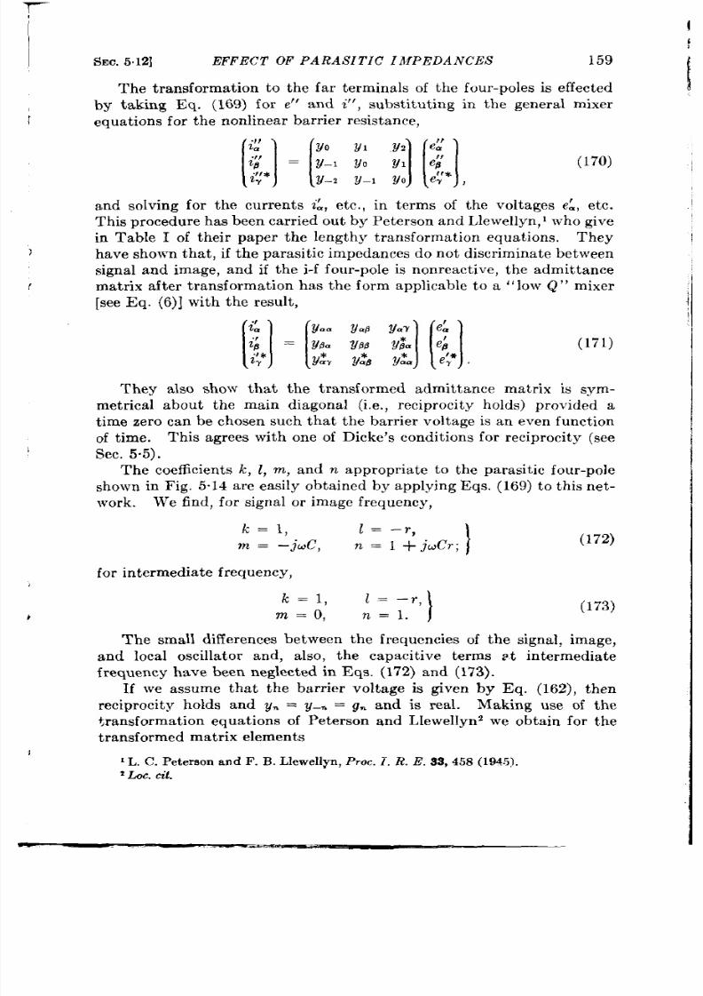
T-
1
SEC.512]
EFFECT OF PARAS ITIC IMPEDANCES
159
The t r ansformat ion to the fa r termina ls of the four -polesis effect ed
by taking Eq. (169) for e“ and i“
, subst itu t ing in the genera l mixer
(
equ at ion s fo t he n on lin ea r ba rr ier r esist an ce,
and solving or the cu r ren t s i:,
e c., in terms of the volt ages e~, et c.
This pr ocedu re has been ca rr ied ou t by Pet er son and Llewellyn ,’ wh o give
in Table I of their paper the lengthy t ransforma t ion equat io s.
They
ha ve shown tha t , if t he parasit ic impeda nces do n ot discr imin ate bet ween
signa l and image, and if the i-f fou r -pole is nonreact ive, the admit t ance
r
mat r ix a fter t ransforma t ion has the form applicable t o a ‘‘ low Q” mixer
[see Eq. (6)] with the resu lt ,
They a lso show that the t ransform d admit tance matr ix is sym-
metr ica l about the main diagona l (i. e., reciprocity holds) provided a
t ime zero can be cho en such tha t the ba r r ier voltage is an even funct ion
of t ime. This agrees with one of Dicke’s condit io s or r eciprocity (see
I
Sec. 5.5).
The coefficien t s k, 1, m, and n appropr ia t e to the parasit ic fou r -pole
shown i Fig. 5“14 a re easily obta ined by applying Eqs. (169) to th is net -
work. We find, for signa l or image frequency,
k=l,
1 = –r ,
m = —jcOC, n = 1 +j&’r ;
}
I
for in t ermed ia t e fr equency,
k=l,
1 = –r,
m=O,
n=l.
)
(173)
The small differ ences between the fr equencies of the signa l, image,
and loca l oscilla tor and, a lso, the capacit ive terms at in t ermedia te
fr equency have been neglect ed in Eqs. (172) and (173).
If we assume tha t the ba r r ier volt age is given by Eq. (162), t hen
reciprocityy holds and q. = g–~ = g. and is rea l.
Making use of the
t r ansformat ion equa t ions of Peter son and Llewellynz we obta in for the
t ra nsformed mat rix elemen ts
1L. C. P et erson a nd F. B. Llewellyn , P roc. 1. R. E. S3,458 (1945).
2LX. m“l.

160
FREQUENCY CONVERS ION
[S rm 512
A’yL= = rz(go – g,)[go(go + gz) – Zg!l +~(29~ – 9; – 9;)
A’y& = A’y& = g,[l + r (go – gz) –
~~1,
Ay& = r(gogj – g;) + Yz,
(174)
A’gje = P(go – g.z)[go(g, + g,) – 2g;] + 2r(gi – g?) + go(l + /.12),
where
and
A’ = r3(go – gz)[go(g
We are now in a
p =
UC?-,
+
gz) –
29;1 + r’(3g: – 29? – 9;) – ~90@ + P’)
+1+/.lZ.
posit ion to find numerica l va lue of the crysta l-
ca rt ridge mat rix for a ssumed ba rr ier ch ar act er ist ics.
To find the “char-
acter ist ic losses and impedances, however , we must fir st t ransform the
matr ix to rea l form.
T ransform ation of the Matrix t Real
F orm .—Th e transforma tion t o
rea l form is accomplished by adding an appropr ia te react ive four-pole
t ransformer to the r -f terminals. This transformat ion becomes unique
if t h e fin al impedan ce level is specified.
Th e con ver sion loss, h owever , is
independent of the impedance level and th choice of the la t ter will be
ba sed on con sider at ion s of simplicity in t he fina l equ at ion s.
Equat ion (171) represen ts a mixer with th ree terminal pairs. To the
two pairs of r -f terminals are now added a pair of ident ica l four -pole
t ra nsformer s. Th is con cept ua l pr ocess cor respon ds t o a ddin g ph ysica lly
a single fou r-pole t ran sformer to th e single physica l r -f terminal pa ir .
The four-pole t ransformer is represen ted by equations similar to
Eq. (169):
em = ae~ + bi~,
i= = ce~ +
di~
)
(175)
with ad – cb = 1. The unpr imed quantit ies r efer to the new mixer
terminals.
The same Eqs. (175) apply to the image fr equency with y
subst ituted for a . The cor r esponding equat ions for the i-f termina ls
ar e tr ivia l, since no t ransformat ion is made there:
Employing an analysis similar to tha t used in the case of the parasit i~
four -poles, we obta in for th e final matr ii (unpr imed quantit ies)

T-
!
1
SEC,512]
EFFECT OF PARAS ITIC IMPEDANCES 161
L
(ada – c) (d – bYL) * + ab”ly~,[’,
1
4
yb(d —Mm)* + b *Y:oY:w
+@ — Mm)* + b
*Y;aY&,
(177)
YaY
Ag~@+ 2[by&(by&ay&) * + yj.(d – bY:a) *1
These t ransforma t ion equat ions, (177), a r e genera l and apply even
if t he fou r-pole t ra nsformer is dissipa tive.
It can be show-n tha t weak
and full r ecipr ocit y a re indepen den tly pr eser ved by t he t ra nsforma tion
)
equations.
As a simple method of effect ing the desir ed t r ansformat ion to rea l
f
form we take the st ructu re of the fou r -pole to consist of a susceptance
– b~a canceling the imaginary pa r t of y& followed by a length @ (in
unit s of k/27r ) of t ransmission line of character ist ic conductance go. It
can easily be shown by applying Eqs.
coefficien ts a , b, c, and d a re given by
a = cos +,
c = –j(b~. cos @ + gO sin o),
If now we choose go a nd 4 by pu t t ing
(175) t o th is st ructu re tha t the
b=
–j sin @
go ‘
(178)
d= –~sin++cos~.
– 92,
(179)
(180)
the t r ansformed mat r ix is r ea l. Subst it t ing Eqs. (178), (179), and (180)
in Eq. (177) we find
A=],
g.. 9:-,
g.fl = gk flSec ‘5
I
g.? = 9L,,
gd. = gja sec 4,
2b&b~a
I
(181)
9!5’8= Cis + /
9..
– 9:Y
In obta in ing these resu lt s y& has been taken to be rea l. This assump-
t i n does not involve any rest r ict ion of genera lity or any assumpt ion
about r eciprocity, as we can see by Eq. (9), which shows t a t a t ime
zero may a lways be select ed to cancel the phase factor of y&.
In the
even t tha t weak reciprocity holds, as assumed here, th is same t ime zero
,
makes el an even funct ion of the t ime (see Sec. 5.5).
We are now in a posit ion to assume a cur ren t -volt age character ist ic

162
FREQUENCY CONVER S ION
[SEC.512
of the bar r ier and to ca lcu la te the character ist ic losses and impedances
of ou r mixer .
Choosing Eq. (160) for the bar r ier character ist ic, we see tha t the
admit tance matr ix of the bar r ier hasthe form of Eq. (164). The matr ix
Y’ is given by Eq. (174) and the final rea l mat r ix Y is given by Eq. (181).
L;
indb
15.5
12.6
1,0
10.59.79.08.37,6 7.1 6,5 5.95.354.84.2 3,52.8 2.0 0
1
0.9-
0.s -
(5)
0.7-
0.6-
a
- 6,5
-7.1 ~
q3
0.5-
(4)
-8. ‘<m
0.4 -
-9.0
-9.7
0.3-
-10.5
0.2-
-12.6
0,1-
-15.5
0
0 0.1 0.2
0.3 0.4 0.5 0.6 0.7
0.8
0.9
1.0
‘1
F IG. 5 .17.—The syn t het ic cr yst a ls of Table 5.4 plot t ed on a (q – t J dia gr am (s eeF ig. 5.S ).
As a numer ica l example let us take
eo=O
aA = 500 ~mhos .
Table 5.4 lists the cha racter ist ic losses obta ined for var ious assumed
values of e 1, r , and C. In Fig. 5.17 these synthet ic crysta ls have been
plot ted as poin ts on an (cl,c:)-diagram, expla ined in Sec. 5“7. It is
in terest ing to note tha t a t low loca l-oscilla tor dr ive (ae 1 = 4) the bar r ier
capacitance is the principa l factor limit ing per formance, whereas at a
h igher va lue of ae, (6) the spreading resistance is the main factor . The
#
i
‘L
,
{

SEC.
513] EFFECT OF A i“ARIAIILE BARRIER C,4PACITA.Y (’I;
163
general dist r ibut ion of the synthet ic crysta ls o the (cl,cJ )-Li~gram is
closely similar to tha t for the silicon crysta ls, plot ted in Fig, 510.
I
‘r.4SLE54.-~HARA(TTl;n1.Tlc~ONVERSIONOSSES(~,) FORSYNTIII;TICRYSTAL
lLECTIFIERS*
ae, r , ohms c, /lpf p = Ucr
L,, d!)
L,,
db t L,)db
——
4.0
0
0 0
‘
5,00
4 85 4.97
4.0
30
0 0
5.67 5.70
5 65
4.0 30
0.3 0.17
7.15 6.91 7.15
40
30
0.6
0.34
9.46
9.18 9.44
60 0 0
0
4,22
3,78 4.12
!,
60 30 0
0
5,61
6,24
5 29
6.0 30 0.3
0.17
6.10
6.60
5 91
a
60 30 06
0 34
7 42
7.60 I 7 41
*For defir ,it ionso[Lo, Lx, e t c ,sw TuMe5 1. O tl,e rq t~n!,,t ie azt r c—
r = n~read ing re~i~ (nnce ,
C = ba r rier ca pwit a nce,
u = 2r fr equ eu .y,
e, = local-mcillmtor voltwzc a,,,ulitudc,
m = exINmenlul fuct . r O[+C cimracleri. tic (seeEq. (160)].
L,, db
4,13
4.90
7.05
9.64
3.03
3.82
4 84
6 94
L,, db
5 02
5.75
7.15
4,23
.
,..
5.13. Effect of a Variable Barr ier Capacitance.’-In Sees. 5.12 and
5.13 there have been explicit ly in t roduced the parasit ic impedance
b
elements C and r of the equiva lent circu it
c
of a crysta l rect ifier and their eff ct on
%
the m ixin g pr oper ties of t he r ect ifier det er -
mined. The approximation was made
that the barr ier capacitance is a constant ,
independent of the voltage across it .
This assumption is known to be untrue;
A
B
FIG. 5.1S.—Equivalent cirruit
it will now be abandoned and the theory
of a cr yst al r ect ifier wit h variable
genera lized by permit t ing the bar r ier bar r ier capacitance”
capacit ance to vary with applied volt age. Var iability of the bar r ier
,.
capacit ance can produce in terest ing and st r iking effect s, which wi l be
considered in some deta il in Chap. 13, In th is sect ion the admit tance
<
mat r ix of the genera l bar r ier with nonlinear capacitance will be der ived.
The resu lt will t h row some ligh t on the genera l problem of reciproc ty.
We sha ll see t at reciprocit y can never hold exact ly in the germ-a l
case. .4 qua lita t ive explana t ion will be given of the exper imen ta l fact
tha t reciproci y viola t ions are almost a lways in the direct ion of causing
the loss from signa l to in termedia t e frequency to exceed the loss from
intermedia t e frequent y to signa l.
The equiva len t circu it her e is that of Fig. 5.18. The resistance R
‘ S ee H. C. Tor rey, “Th eor y of t he N ega tive I-f Con du ct an ce of N ’or th ’s Welded
Con ta ct Germa nium Rect ifier s,” RL Repor t N o. 55, Ma y 22, 1945.

164
FREQUENCY CONVERS ION
[SEC.513
is t he non lin ea r r esista nce of t he ba r ier , Cit s onlin ea r ca pa cit ance, a nd
r t he linear spreading resistance; r may include other linear losses of th e
ca r t r idge (for example, whisker and wax). The current i th rough the
rect ifier will be composed of these t wo parts:
il = j(e),
dQ
a’ ‘z”
llere e is t he bar r ier volt age; f(e) is t he low-frequency
cur ren t o volt age, and Q is the charge on the ba r ier .
cur ren t is
i = j(e) + ‘~.
(182)
(183)
depen den ce of
Thus the tota l
(184)
Asin Sec. 5.11, iande are taken to be composed of frequencies, o,
andnt i(n =2,3,..
.), where u is the loca l-oscilla tor (angular) frc-
quencv, and it ~vill again be assumed that the components at signal, i-f,
image, and harmonic sidebands a re small enough to be considered as
var ia t ions of i and e.
Thus,
bi = Re
z
iPe7%J,
(185)
P
z
?ie=Re
ePe>b#,
(186)
P
where b~ includes the frequencies @ and no + ~, (n = 1, 2 3, . . .), that
is, signa l, i-f, image, and harmonic sidebands.
The variat iona l equat ion tha t replaces Eq. (153 is
(187)
where e’ = de/ d t. The s cond term on the right must be included since
i is now an explicit funct ion of e’, inasmuch as Eq. (184) may be r it ten
in the form
dQ
i =j(e) + e’~.
(188)
Th is givesl
( )
=f(e)+$ @Q,
(189)
a’i dQ
2=Z”
(190)
I Th e u se of j’ (e) t o in dica te cliffer en tia tion wit h r espect t o t he a rgumen t sh ou ld be
diet in gu ish ed fr om t he u se of t he prim es elsewh er e t o in dica te differ en tia tion wit h
r espect t o t he t im e.
I
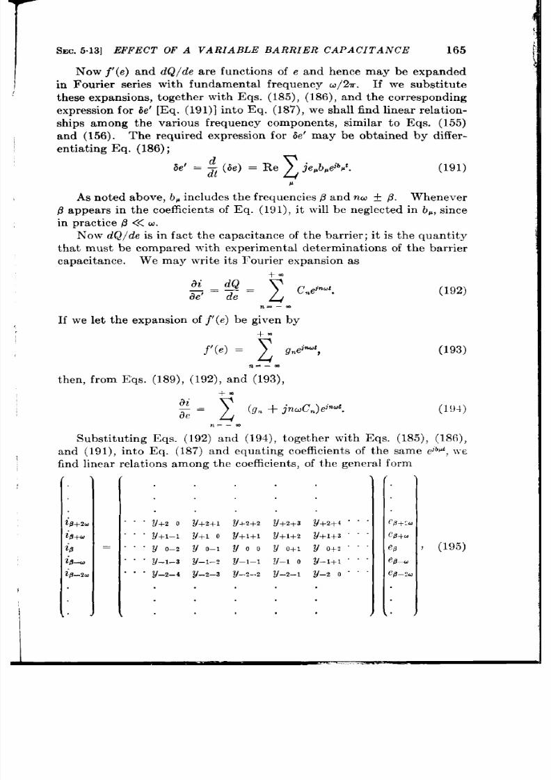
SEC.5.13]
EFFECT OF A VARIABLE BARRIER CAPACITANCE
165
N ow j’(e) and dQ/ d e are funct ions of e and hence may be expanded
in Four ier ser ies with fundamenta l frequency u/27r . If we subst itu te
t hese expa nsion s, t oget her wit h Eqs. (185), (186), an d t he cor respon din g
expr ession for t ie’ [E q. (191)] in to Eq. (187), we shall fin d lin ear r ela tion -
sh ips among the var ious frequent y components, similar to Eqs. (155)
and (156). The required expression for ~e’ may be obta ined by differ-
en tia tin g Eq. (186);
de’ = $ (~e) = Re
z
jePbPeibJ.
(191)
P
As not ed above, b, includes the frequencies@ and rw f P. Whenever
~ appears in the coefficien ts of Eq. (191), it will be neglected in b,, since
in pract ice @<< w
Now dQ/ d e is in fact the capacitance of the b rr ier ; it is the quantity
tha t must be compared with exper imenta l determinat ions of the barr ier
capacitance. We may writ e its Four ier expansion as
4.
ai
–dQ=
z
Cnein.t
u–x
. (192)
.=—.
If we le the expansion of ~(e) be given by
+.
j’(e) =
2
g.eiwt,
(193)
.=—.
then , from Eqs. (189), (192), and (193),
+.
d i
a~ =
s
(q ,, + @d3n)ein@t .
(l$)J)
,,=—m
Subst itut ing IZqs. (192) and (194), toget er with Eqs. (185), (18 ),
and (19 1), into Eq. (187) and equat ing coeff cients of the same ejb@, I ve
find linear relat ions among the coefficien ts, of the genera l form
i
I
—
. . .
y+z o !/+2+1 y+z+z y+2+3 Y+2+4
. . .
y+I–I y+I o y+I+I Y+I+z y+1+3
. . .
yO–2yo–1y 00 Yo+1Yo+2 ““”
. . .
y–1–3 Y–I–? U–I–I Y–I O Y–1+1
. . “ y_z_4 y_z–3 y–2–2 y–2–1 y–2 O “
l--
166
FREQUENCY CONVER S ION
[SEC.5.13
where
ymn = g. + jnwCn.
(196)
If we neglect harmonic sideband volt ages as befor e, th is reduces to
(1[
=
go + juco
gl + jcdcl
1[1
2 + jd72 e=
= g–1
go
gl
(197)
i;
9–2 — juC–2 g–-l – jaC–1 90 — jOCO e!
Now because of the rea lity of ~(e) and dQ/ d e
in Eqs. (192) and (193)
we must have
g-n = 9:,
and
(198)
c+ = c;.
If, fu r ther , a t ime zero can be found such that e, the bar r ier volt age,
is an even funct ion of the t ime, then , using this t ime zero, we have
g_n = gn and C_m =
C.; hence with Eq. (198) we see that C. and gn are
rea l. The exist ence of th is t ime zero, however , does not make the admit -
t ance mat r ix of Eq. (195) or of Eq. (197) symmetr ica l. Indeed reci-
procity now cer ta in ly fails if th is t ime zero exists. The admit tance
matr ix of Ills. (197) is observed by Eq. (198) to have the symmet ry
requ ired by a low-Q mixer , as it should according t o our assumpt ions.
Some light is th rown on the genera l problem of r ecip ocity fa ilure
by Eq. (197). It should be noted tha t if gmand C. can be made simul-
taneously real by proper choice of t ime zero (and this should be at least
a ppr oximat ely possible), t hen t he r ecipr ocit y fa ct or
H=WI’l
It appear s from the exper imen ta l work of Smithl and pker2 that
H
for normal crysta ls the r eciprocity factor ‘U , in the presen t case
Y&a
91 + juCi
g-1
is grea ter than or equal t o unity.
Except ions t o this ru le have been
found by Apker~ in the case of welded-con tact germanium rect ifier s
for specia l bias point s [not those bias poin ts, incidenta lly, which give
1R. N. Sm it h, “Th e Th eor y of N fixer s in Terms of Nfea su ra ble Mixer Constants,”
NDRC 14-259, P urdue Univ., Mar. 24, 1944.
2 L. Apker , “ Not e on Recipr ocit y F ailur e in Cr yst al Mixers,” NDRC 15-931-16,
GE Co., Mar . 9, 1945; and “Theory of a Double Mixer for Spect rum and Glyzer
Applica tion s,” NDRC 15-931-16, GE Co., Apr . 3, 1945.
s Pr iva te communica t ion .
SEC.5.14]
HARMON IC REINFORCEMEN T
167
r ise t o nega t ive i-f conductance (see Chap. 13)]. The theory of var iable
ca pa cit ance given h er e does n ot , of cou rse, exclu de such a possibilit y.
It is not ewor thy that weak reciprocity [Eq. (52)] holds for the matr ix
of E q. (197) in eit her of t he ext rem e ca ses, uC1 <<gl, uC2 << gz or uC1 >> gl;
~cz >> gz; on t he ot her hand full reciprocit y fa ils by a considera ble fa ct or
in the la t t er case. As noted above, weak reciprocity always holds
exper imenta l y although full reciprocityy fa ils for many germanium
crystals.
The subject of the effect s of var iable capacity is discussed fur ther
in Chap. 13, where the admit t ance mat r ix of Eq. (197) is made use of in
expla in ing these effect s.
5.14. Harmonic Reinforcement .-The phenomenologicrd theory of
mixers developed in Sec. 5.3 et seq. is based, among other things, on the
assumpt ion that harmonic voltages a re zero at the terminals of the mixer .
It does not appear feasible t o at t empt a genera liza t ion of th is theory,
which in ludes ha rmonic volt ages at t he mixer terminals.
In the phys-
ical t heory discussed in Sec. 5.11 and t he following sect ions, t here have
been given genera l result s, which hold if harmonics a re present , but
absence of harmonic voltages has been assumed, even at the barr ier ,
w en numerical examples we e given An adequa te mathemat ica l
t rea tment of harmonic effect s is, in fact , ver y difficult ; her e only a simple
n umer ica l example will be given wh ich w ll a t lea st in dica te t he qu alit at ive
na tu re of such effect s.
Let us as ume the low-frequency case, in which the current is a func-
t ion of the voltage of the form
i = j(e).
(199)
Values of conver sion loss w ll be calcula ted under t he t wo condit ions
(a ) sh or t cir cu it ed ha rmonics, a nd (b) secon d h armon ic open-cir cuit ed,
other ha rmon ics shor t -cir cu it ed.
The value of loss for other react ive
termina t ions of the second harmonic presumably lie somewhere in
between. Case a has been t rea ted above (Sec. 5.11). We must now
con sider Ca se b. The voltage e will be given by
e = eO+ el cos cot + ez cos 20t ,
(200)
and the current by
.
~=
2
i .os nd.
.=0
(201)
The problem, then, is t o choose e, so that & = O, tha t is, so tha t th6
second ha rmon ic is open -cir cu it ed .

168 FREQUENCY CONVER S ION
IsEC.5.14
If we choose j(e) as in Eq. (160) then
‘=A (e”’0[2~(~e1’ei””’1r 2~m(ae’)e’’mo’l -11’ ‘202)
—. -m
wh er e the 1’s ar e modified Bessel funct ions of the first kind,
I.(z) = j-”J .(jz) .
The second-harmonic cur ren t L is given by
i2 = Ae.eo
z
In(cfeJIm(ae2)ei’Jt(2”J+”)
(Zm nx - *2)
+-
r
12
Aeaeo e2id
12(
I–m)(ael)Im (aeJ
—.
+.
+ ~–2i.1
z
1
Z_l(l+~)(aeJ I~(ae,) . (203)
—
Since I_~ = I-,
+-
iz = 2Aeee0 cos 2u t
2
12-2m(ae1)Zm(ae2).
(204)
—.
The condit ion that iz = O is (if ael = x, aez = –y)
As an example, let us take z = 4. By a method of successive approxi-
mat ions we find
y = 1.582,
(206)
and obta in for t he Bessel fun ct ion s
lo(y) = 1.731,
I,(y) = 1.066,
I,(y) = 0.384,
~,(y) = 0.096,
I,(y) = 0.019,
l,(y) = 0.003,
16(y) = 0.0004,
1,(4) = 11.3019,
1,(4) = 9.7595,
1,(4) = 6.4222,
1,(4) = 3.3373,
1,(4) = 1.4163,
16(4) = 0.5047,
~6(4) = 0.1545,
17(4) = 0.0413,
~6(4) = 0.0098,
19(4) = 0.0021,
1,0(4) = 0.0004.
SEC.5.14]
HARMONIC REINFORCEMENT
169
Using these values, we find for the Four ier expansion of d i/ d e = j’(e),
‘ ( e )aAe”eOzane’*’Z ’ e ’ n ” t
207)
where
ao = 6.929, a3 = – 1.717,
al = 4.355,
ad =
– 0.778, et c.
az = O,
In calcula t ing conversion lo s, the second-harmonic sidebands ar e
assumed to be open-circuit ed, whereas other harmonic sidebands ar e
sh or t-cir cu it ed. Th e gener al admit tance matr ix, Eq. (156), th en r edu ces
to
[1
G Gafl Ga7
~Ae_eO G; Gm Gae ,
(208)
Gav Gafl G..
where
F om these we find [see Eqs. (123a , (126), and (143)]
c1 = 0.689,
63 = 0.821>
~z
0.947,
wh ich gives [see Eqs. (141) and (142)]
L, = loss for shor t -cir cu ited image = 5.5 db,
L, = double sideband loss = 5.o db,
1
(210)
L~ = loss for open-cir cu ited image = 3.9 db.
These values sho ld be compared with the cor responding values for
el = 4 and for all harmonics shor t -cir cu it ed (as found in Sec. 5.11), viz.,
L, = 4.85 db,
L, =
5.0 db,
Ls = 4.1 db.
The resu lt of open-circu it ing the second harmonic does not ther efor e
produce significant changes in conversion loss, for t e example chosen.
It seems unlikely that the genera l case will differ grea t ly in th is respect .
170
FREQUENCY CONVER S ION
This lends suppor t to the assumpt ion , genera lly
IsEC.
5.15
made, tha t a good
approxima tion to the performance of the mixer is obta ined by assuming
shor t -cir cu it ed ha rmon ic volt ages .
Th e pr ecedin g con clu sion s wit h r ega rd t o t he effect of open -cir cu it in g
the second harmonic a re perhaps open to object ion for the following
reasons. The rect ified curren t will be different for the two cases of a
shor t circu it and an open circuit a t the second harmonic.
In or din ar y
crysta l r ect ifiers the conversion loss is on ly a slowly varying funct ion
of crysta l cu rren t, on ce th e la tter quant ity is sufficien t ly la rge.
For the
example ch osen here, h owever , this is not t ru e.
P er haps t h e compa rison
would be fa irer if the values of Eq. (210) were compared with the losses
for shor t -circu ited harmonics a t th e same
rect if ied current .
The rect ified
cur ren t , assuming zero d-c bias,
for the example given here (open-
circu ited second harmonic) is easily ca lcula ted. It is
iO = A(ao – 1) = 5.93A
when ao is given by Eq. (207).
Using the va lue of ael tha t gives th is va lue of io for the case of all
h armon ics sh or t-cir cu it ed, -we fin d in t his ca se
L, = 5.4
L, =
5.3
L, =
4.7
On compar ing these with Eq. (210)
difference, except for L,, where there is
db ,
db ,
db .
we again find no signific nt
an apparent improvement of
0.8 db on open-~ ircuit ing the second harmonic. ” - -
6.16. Con ver sion wit h a Su bh armon ic Loca l Oscilla tor .-Th e pr oblem
of con st ru ct in g a st able t un able C-Woscilla tor t ha t will pr ovide su fficien t
power for use as a loca l oscilla tor becomes very difficu lt a t frequencies
above 3 ,000 Me/see (l-cm wavelength). An alterna t ive is to use the
ha rmonic power of a lower-frequency oscilla tor . This harmonic power
can be genera t ed by a crysta l rect ifier .
One method is to use two
tryst als, on e for gener at in g th e h armonic power , and t he oth er for mixing.
A second possibility is to use on ly one crysta l wh ich perf rms both
funct ions. The la t ter a lterna t ive eems preferable from the poin t of
view of econ om ica l cir cu it design .
A possible disa dva nt age, h owever , is
tha t the fundamenta l power require to genera t e sufficien t harmonic
power for low mixer convers on loss is la rge and may be expected to
pr odu ce con sider able excess n oise ou tpu t a t t he in termedia te fr equ en cy.
Exper imen ts designed to test the feasibility of a “harmonic mixer”
of the second type were made by Fa lkoff. 1
‘I’h is work was exp lor a t ory
in natu re and was performed at frequencies lower than those for which
1D. L. Fa lkoff, RL Repor t No. 958, Ma r . 11, 1946.

!?iEc.5.15]
‘.
SUBHARMONIC WCAL 0S f7ZLLA TOR
171
a harmonic mixer is needed because of the rela t ive availabili y of com-
ponen ts. The work was terminated by the end of the war before it
cou ld be extended to the high frequencies of in t erest .
Figure 5.19 shows a block diagram of the Fa lkoff apparatus. The
loca l oscilla tor was a t a wavelength of 6.4 cm and the signa l a t about
Conventional
mixer
Detector
(3.2 cm)
1
q’
t t
A
Preamplifier
—
AmpMier
B
t
UE1-EEl
IG.5.19.—Block d ia gr am of appa r a tu s u sed in t es tin g a h a rmon ic m ixer .
Fundamentalpowerin milliwatts
FIG.5 .20.—Typica l per formance of a harmonic mixer .
Loca l oscilla t or a t a wave length of
6.4 cm , s gn al a t 3.2 cm .
3.2 cm. A direct compar ison of conversion with the harmonic mixer and
conversion with a convent iona l mixer a t 3.2 cm was made.
(Th e same
signal genera tor was used for bot mixers.
At switch posit ion A it
was coupled to the convent iona l mixer , a t B
to
the harmonic mixer . )
It was found tha t sufficien t second-ha rmon ic power was available from
the harmonic mixer to provide loca l oscilla t ions for the 3-cm mixer . A

172
FREQUENCY CONVER S ION
[SEC.5.15
noise diode (not shown) made possible a direct measuremen t of the noise
t empera ture of the ha rmonic mixer .
Typica l result s for the ha rmonic mixer and commercia l 1N23B
crysta ls a re sho n in Fig. 5“20.
These data were taken with the ha r-
monic mixer ma tched to the externa l circuit s a t both 3.2-cm and 6.4-cm
wavelengths.
Some notewor thy fea tures of these result s a re
1.
2.
3.
4.
The lowest noise figure occurs a t about 0.5 mw of 6.4-cm power ,
wh ich is a bou t t he opt imum loca l-oscilla tor level for con ven tion al
mixers.
The noise tempera ture increases linear ly with the 6.4-cm power
upto300r40mw. This is not apparent from the figure because
the input power is plot t ed on a log r ithmic scale. Above 40 mw,
the noise t empera t re depar t s from linear ity in the direct ion of
lower va lu es of n oise t emper at ur e.
The conversion loss decreases slowly with 6.4-cm power above
1 mw, approaching a constant value of about 8 db when the
6.4-cm power exceeds 10 mw.
The noise figure changes slo ly, genera ly remaining below 20 db
over a range of loca l-oscilla tor power rom 100 pw to 10 mw.
Fa lkoff found tha t t he lowest conversion loss did not occur for
matched harmonic (3-cm band) power out of the harmonic mixer , but
tha t the lowest loss was obta ined when the 3-cm output power was
decreased by mistuning by a factor of about 2 from the matched condi-
t ion . This lowest loss was about 2 db less than tha t for the case of
m at ch ed 3-cm power .
An effect probably of importance, but not invest igated by Fa lkoff, is
tha t of select ive t un in g a t the 6.4-cm terminals of t he harmonic mixer .
To see why this effect might be important , the mixing process in a
second-harmonic mixer might be considered. Let us take the loca l-
oscilla tor frequency as $U and the signal frequency as o + B. Thus the
signal, beat ing with the second harmonic u of the local oscilla tor , is
conver t ed to the intermedia te frequency ~. However , the signal a lso
bea ts with the fundamenta l frequency of the local oscilla tor and is
thereby conver ted t o ~u + ~, a sideband of t he local-oscilla tor frequency
Au, and this conversion process should be more efficient than the con-
ver sion t o in termedia te fr equ en cy.
Consequent ly, it should be of he
u most imp rtance to insure that power at &I + 19is not dissipated by
transmission a ong the matched loca l-oscilla tor line. A filt er circuit
inser ted in thk line to reflect t he & + @ ave would seem most desirable.
It would also serve the purpose—if a rranged as a bandpass filt er passing
only &-of suppressing the noise sidebands of the loca l oscilla tor . If

F
SEC.5.16]
IIARMON IC GENERAI’IO,V
I
such a filt er were to be inser ted in the iu-line, it s
chosen with care to insur opt imum phase of the
173
posit ion should be
(*u + ~)-sideba nd
in the mixer . The parasit ic $ti + @ should play a much more impor tan t
r ole in the harmonic mixer than does the image frequency in a conven-
t ion al m ixer .
6.16. Harmonic Genera t ion .—In the previous sect ion one solu t ion of
the problem of providing local oscilla t ions at very h igh frequencies—
the “ harmonic mixer “-was examined. An a lternat ive scheme is to
use two crysta ls—one to gen ra te harmonic power at the desir ed local-
oscilla tor fr equency, and the other to act as a conven t iona l mixer in
which th is harmonic power beats direct ly with a signal to produce the
In the exper imen t s of Falkoff descr ibed in the previous sect ion , it
was found that the ou tpu t of 3.2-cm power , conver ted from 6.4-cm power
by the mult iplying crysta l, r anged fr om 11 db to 14 db below the input
6.4-cm power , and was ample to provide local oscillat ions for a conven-
t ional 3.2-cm mixer . The efficiency of harmonic genera t ion decreases
with hcreasing fundamenta l fr equency, however .
Montgomery has
found that the best ha rmonic-genera t ion crysta ls (german ium welded-
contact r ect ifiers) produce second-harmon ic power abou t 17 db down
from a funda en ta l at 3.2 cm, with an input power of 30 mw.
Although
~.~=non ic genera t ion of millimeter waves from a fundamenta l of 1.2 cm
has been studied, no absolute power measurement s a t the ha rmonics
have been made, and the efficiency is not known in th is most in terest ing
case.
Montgomery has, however , made extensive compar isons of the
rela t ive ha rmonic genera t ion fr om the 1N26 (silicon l-cm mixer crysta l)
rect ifier and from the welded-con tact german ium rect ifier of H. Q. Nor th
(see Chap. 13), finding that the german ium rect ifier s at their opt imum
d-c bias wer e sligh t ly super ior to the 1N26 crysta ls in the product ion of
1.6-cm waves fr om a fundamen a l at 3.2 cm.
Their super ior ity was
much greater in the genera t ion of the th ird ha rmonic (0.4 cm) from a
f unclamen ta l at 1.2 cm. F igure 5.21 shows the rela t ive per formance in
th is case.
The nota t ions “ bias,” “open-circu ited,” and “ shor t -cir -
cu ited” r efer t o t he d-c bias con dit ions.
It was found that the opt imum
bias for the germanium crysta ls was cr it ica l. The ordina te of this plot
is the open-circu it direct voltage obta ined rom a crysta l used as a
r ect ifier of t he h armonic power .
Recen tly Nor th 3 h as impr oved t he h armon ic gen er at ion of h is cr yst als,
I D. Mon tgomery, RL Repor t No. 818, Oct . 23, 1945.
2Lot . cit .
z H . Q. Nor th ,
“A Com par ison of Silicon a nd Germa nium Micr owa ve Cr ysta ls
as Harmonic Genera tor s of 4 mm. and 6 mm. Waves, ” GE Repor t , J an . 15, 1946.

17%
FREQUENCY CONVEILS 1ON
[SEC.
517
in par t icular the genera t ion of the third harmonic from a 1.2-cm funda-
men a l, by going to ~velded contact s of very mall dimensions. He
used whisker deflect ions of only 0.00012 cm and a welding current of
50 ma as cont rasted with 0.0005 m and 250 ma for the normal case
(see Sec. 13”1). These small-contact , welded rect ifiers produced 10 to
20 db more output (0.4-cm) power than convent iona l 1N26 rect ifiers
a t the same input (1.2-cm) power .
5.17. Modula t ion.—Crysta l rect ifiers a re somet imes used as modu-
la tors, i.e., asagent s t opr oduce sideba nds of a ca rr ier . Ch-yst almodula -
t ion fa lls in t o two ca t egor ies: (1) conver sion of slow-fr equencysign a lt o
high-frequency
high-frequency
FIG.
sidebands of a local oscilla tor ; (2) conversion of a pure
ca r r ier t o sidebands. In the first case, the mixer is
80
60
—r%PJA
I
v in microvolt
5.21.—Rela t ive per forman ce of N26 r ect ifier s a n d german ium welded -con t act
r ect ifier s in t h e gen er a tion of 0.4 cm power fr om a fundamen t al a t 1.2 cm .
dr iven by a high-frequency loca l oscilla tor and, in t he second, by a low-
frequency (modula t ion-frequency) oscilla tor . The first , case is just the
in ver se of~th e familia r m ixer pr oblem we h ave been con sider in g u p t o n ow,
a nd t he secon d in volves some n ew pr in ciples.
The first t ype of modula -
t ion has been used by Apker in his double-mixer spect rum ana lyzer l
while t he second t ype has been employed by Pound2 in one of his met hods
of fr equency st a biliza t ion of oscilla t or s.
Aa was shown in Sec. 5“9, modula t ion of the first t ype ma be t rea ted
with the same mathemat ica l theory us d for ordina ry mixers. If Lafl
is the conversion loss from a Klgh-frequency a signal sideband to a low
bea t frequency /3, the conversion loss for the reverse process is just
LB. = ly@./ y.d[ 2L.6, where lyd./y.~l is the reciprocity factor discussed in
Sec. 5.9. In all silicon rect ifiers observed so fa r , t he exper imenta l va lue
1See L. Apker , E. Taft , and J . Dickey ,”
Th eor y of a Dou ble Mixer for Spect rum
An alyzer Applica tion s,” OEMsr -931 Repor t 931-17, GE Co., Apr . 2, 1945.
z R. V. Pound,
“An Im pr oved F requ en cy St abiliza tion Syst em for Micr owa ve
oscilla tors,” RL Repor t N o. 837, Oct . 26, 1945.

SEC.5.17] MOD ULA TION 175
of lY d=/ VaPl is close to
unity, whereas, for german ium rect ifier s, th is quan-
t ity is oft en found to be much less than un ity. The process of modula t ion
is, t herefore, in the case of germanium, oft en considerably more efficien t
than the inver se process of mix ng. Observed values of lyda/yaPl for
german ium have been f oundl to r ange between 1 and ~.
The second type of modu la t ion , em loying a low-fr equency loca l
oscilla tor , is somewhat simpler in theory than the mixing process con -
sider ed above. The grea t er simplicity ar ises fr om the fact tha t a ll
fr equencies connected by linear r ela t ionsh ips are of the same order , and
that , in pract ice, t here is no impedance t r ansformat ion involved. The
theory of th is proc ss will now be ou t lined.
The modu la tor is shown schemat ica lly in Fig. 5.22. Let ~ = voltage
reflect ion coefficien t at the r -f termina ls.
It will be assumed tha t he
Lou
level carrier
EzDIEE+R_eband’
+Generated side bands
FIQ.5.22.—Block d iagr am of a modula t or whose funct ion is t o conver t a low-level ca r r ier
in to s idebands .
ca r r ier is at a sufficient ly low level so that the r -f admit tance of the
modula tor is completely con trolled by the low-fr equency dr iver . Then
+.
y=
z
y~einb’,
(211)
n=—.
wh er e D is t he modu la tion fr equ en c .
Let the incident r -f cu r ren t wave be given by
+-
1=
2
~W+flpe~(w+.6):
1
.=—.
and the reflected cur ren t wave by
+.
I’ =
z
Y+@e’(+@)’.
n=—.
By defin it ion of t h e r eflect ion coefficien t ,
I’ = 71.
(213)
I Valueagreaterthan one have recentlybeen found by L. Apker (privatecommuni-
cation) in th e case of welded-conta ctgermaniumcrystalsat specialbiaapointe.
(212a)
(212b)
176 FREQUENCY CONVERS ION [SEC.5.17
The incident and reflect ed voltage waves will be denoted by V and V’;
their Four ier representa t ions a re similar to Eq. (212), with V.wd and
V~t i replacing lu+~d and l~nfi, resp ct ively. We have then
(214)
f = –yv = –-yzoI,
where ZO is the character ist ic impedance of the t ransm ssion line a t t ached
to the r-f terminals.
Subst itu t ing Eq. (211) into J lqs. (213) and (214), we obta in
+-
I~+nb =
2
7.–J .+%%
(215)
m.—.
+-
V:+* = –2
z
Y.–nJu+nao.
(216)
m.-.
For the present , sidebands at frequencies ot her than u + @are neglected.
Equat ions (215) and (216) may then be wr it t en
ll=’EI
ll=-z”r[l
(218)
where r is the “ sca t t er ing mat rix, ”
[1
0 71 72
r = 7–1 70
-Y1
(219)
Let us
consider now the specia l case where a pure ca r r ier at frequency
u is incident , and pure sidebands u ~ /3 a re genera t ed with no carr ier .
Evident ly, in th is case,
V:+g = – ZoT ,I.,
V:+ = – .ZOy_,Iu .
)
‘l’h e in ciden t power is
P. = *ZOIIJ ’,
(221)
and the reflected power in the sideband w + L?is
P:g = +2017,1’] 1”[’.
(222)
SEC. 517] MOD ULA TION 177
Th e conver sion loss to th is sideband is then
Similar ly, the conversion loss t o the ot her sideband is
(223)
(224)
These expressions for conversio loss hold also in the genera l case in
which other sidebands are not neglected. Thus,
(225)
If we assume that a t ime zero can be chosen such that the dr iving
voltage (a t frequency 6) 1s an even t ime funct ion , we have ~- = ~~,
a d the sidebands are symmet r ica lly genera ted. In this case,
I
\
1*
yl=–
‘y Cos @d(/9t) .
To
Since Iyl S 1, it is apparent tha t IYII ~ 2/7r , and so the conversion loss
t o the fir st -order sidebands is rea ter than u2/4 or 3.9 db. An ideal
modula tor thus has a loss of 3.9 db to either fir st -order sideband.
As an example, let us neglect react ive effect s in the crysta l and
modula tor , and take the crysta l cur ren t -volt age character ist ic t o be
I = A(e”’ – 1),
which , as n ted above [Eq. (160)], is an approximate representa t ion
of the d-c character ist ic of an actual rect ifier . The r -f admit tance ~vill
then be
dI
dV
— = Aae”v.
Let us assu e for simpl city that Z, = Aa = 1, t h en
where V = Vo cos & is t he low-fr equ en cy dr ivin g volt age.
If aVo>> 1,
2
(
21n2
5.41
71=; l–
—— —
)
. . . .
a Vo as ~
(.
I
178
FRIIQ (J EN CY CON VERS ION
[SEC.5.17
Assuming a value aVO = 10, we fin d
~, = ~ (0.8 6)
and L = l/1711 z = 5.4 db, or 1.5 db above the theoret ica l minimum loss.
Measurements by R. V. Pound,’ a t the 3-cm band on a 1N23B
rect ifier gave L =
6 db, which agrees well with the exampl given here.
In t his example, a ll even -or der sideba nds a re su ppr essed, a nd t he t hir d-
or der sidebands ar e down a bout 10 db below t he fir st -order sidebands.
1Pr iva te communica t ion .
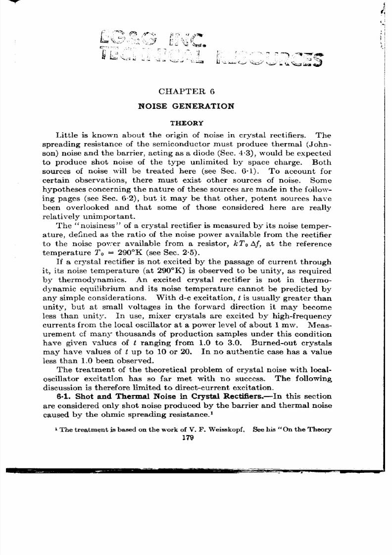
--. .. ——. —
CHAPTER 6
NOISE GENEIU ITION
THEORY
Lit t le is known about the origin of noise in crystal rect ifiers. The
spreading resistance of th e semiconductor must produce thermal (J ohn-
son) noise and t e barr ier , act ing as a diode (Sec. 4.3), would be expected
to produce shot noise of the type unlimited by space charge Both
sources of noise will be t rea ted here (see Sec. 6“1). To account for
cer tain observa t ions, there must exist other sources of noise.
Some
h ypoth eses con cern in g t he n atu re of t hese sou rces a re made in t he follow-
ing pages (see Sec. 6.2), bu it may be that other , poten t sources have
been over looked and tha t some of those considered h re are really
rela t ive ly unimpor tant .
The “noisiness” of a crysta l rect ifier is measured by its noise temper-
a ture, defined as th e ra t io f the noise power available from the rect ifier
to the noise pov:cr available from a resistor , k 7’o A j, at t he r efer en ce
tempera ture TO = 290”K (see Sec. 2 5).
If a crysta l rect ifier is not excited by the passage of curren t through
it , its noise tempera ture (a t 290”K) is observed to be unity, as required
by thermodynamics. An excited crystal rect ifier is not in thermo-
dynamic equilibr ium and its noise tempera ture cannot be predicted by
any simple considerat ions. With d-c excita t ion , t is usually grea ter than
unity, but at small voltages in the forward direct ion it may become
less than unit i~. In use, mixer crysta ls are excited by high-frequent y
currents from the local oscilla tor a t a power level of about 1 mw.
Meas-
urement cf many thousands of product ion samples under this condit ion
have given values of t ranging from 1.0 to 3.0. Burned-out c ysta ls
may have values of t up o 10 or 20.
In no authent ic case has a value
less t ha n 1.0 been obser ved.
The t rea tment of th e theoret ica l pr blem of crystal noise with loca l-
oscilla tor excita t ion has so far met with no success.
The following
6.1. Shot and Thermal Noise in Crysta l Rect ifiers.-In this sect ion
a re considered only shot noise produced by the barr ier and thermal noise
cau sed by t he ohmic spr ea ding r esista nce. *
I The t r ea tmen t is basedon thework of V. F . Weis skopf, Seeh is “On the Theory
179
180
NOIS E GENERA TION
[SEC.6.1
The barr ier of a silicon or germanium rect ifier was shown in Sec. 43
to be somewha t analogous to a tempera tu re-limited vacuum-tube diode.
The mean free path of the elect rons is la rger than the barr ier width
and th e elect ron s fly ov r t he ba rr ier pra ct ica lly un impeded by collisions
or space charge. The discreteness of elect ron ic cha rge and the random
arr iva l of el ct rons a t the meta l (or , in the case of the rever se cur ren t ,
a t the bulk semiconductor ) give r ise to random cur ren t fluctua t ions
commonly r efer red t o as “shot noise. ”
Noise of t his t ype wa s con sider ed
for the case of a tempera tu re-limit ed d ode by Schot tky, who showed
that the mean square noise cu rren t produced by this effect is given by
(1)
in the frequency band
f
t o
f +
Aj. Here e is the elect ron ic cha rge and I
is t he diode cu rr ent ,
?
I
----
rP
P
rz
r l
-----
r
(a)
(b)
F1~. 6 .1.—Schema tic d iagr ams of t h e equ iva len t cir cu it of a cr ys ta l r ect ifier . (a ) Ces e of a
unif rm contact poten t ia l; (b) case
of a distributed contact potential.
If th is formula cou ld be expected to hold for the case of the crysta l-
r ect ifier ba r rier , t h en
1 =1,+1,,
(2)
where 11 and Zz are the elect ron cur ren ts from semiconductor to meta l
a nd fr om meta l t o sem icon du ct or r espect ively (sin ce 11 and
12
a re equa lly
effect ive in p roducing shot -nois e flu ct ua tion s).
Equat ion (1) shou ld hold for the ba rr ier proper . To obta in the tota l
noise from the rect ifier there must now be included the con tr ibut ion
fr om t he spr ea din g r esist an ce.
Her e, idea l con ta cts of u niform con ta ct
potent ia l must be dist inguished from actua l con tact s which , as noted in
Sec. 4.4, probably consist of distr ibuted con tact poten tia ls. This
of Nois e in Conductom , Semiconductor and Crys ta l Rect ifier s,” NDRC 14-133,
May 15, 1943.

SEC.6.1]
SHOT AND THERMAL NOIS E IN CR YSTA4L RECTIFIERS
181
dist inct ion is necesmry for the following reason. In the case of the ideal
uniform contact , the spreading resistance may be lumped together
and assumed to be in series with the barr ier as shown in Fig. 6“la. As
was seen in Sec. 4“4, however , for a dist r ibuted contact potent ia l, the
current flows most ly through local spots of rela t ively low conta ct oten-
tia l. Each of these spots has in series with it its o n local spreading
resistance rkywhich is not shared by the other spots. The barr ier then
consists of a number of these series elements all in shunt with each other .
F inally the spreading resistance r of the ent ire contact is in ser ies with
thk combinat ion. The situa t ion is shown schematically in Fig. 6.lb.
To calcula te the total available noise power the following theorems
concern ing the tota l noise output of a combinat ion of noise sources a re
ut ilized. The proofs a re fa ir ly obvious.
THEORE~ 1. If a number of noise sou ces of different ial (dynamic)
resistance pk are connected in parallel, the mean squares of the noise
cu rr en ts a re a ddit ive; h en ce
z
2=3
‘tk (parallel),
(3)
k
and the tota l available noise power P can be expressed in terms of the
individual noise powers pk in the form,
z
Pk
P=p
1
z
1
I
(parallel).
—
i– —
Pk
(4)
THEOREM 2. If a number of noise sources are in ser ies, the mean
squ ares of t he emf’s a re a ddit ive;
(5)
and the tota l available noise power is given by
P=!
z
Pkpk,
P
k
z
!
(series).
(6)
p= Pk
k
In addit ion there is needed the result of Nyquist l that the available
noise power from an ohmic resistance is
k 2’ Af. Th is well-k nown r esu lt
1H. Nyquist, Phys. Rev., S 2, 110 (1928).
182
NOISE GENERA TION
[SEC.6.1
is usually pr oved by th ermodynamic argument s.
Recen t pr oofsl ba sed
on kinet ic t heory have clear ly shown that thermal noise has the same
natu re and or igin as shot noise.
Weisskopf also der ives t he n oise power
of a nonohmic resist ance in which the elect rons gain more energy than
k T from the field in one free path . A resistance of this type is sa id to be
‘‘ over loaded. ” It is possible that the local spreading resist ance of some
barr ier spot s of low contact poten t ia l would be of this character .
The simple case of a uniform con tact potent ia l is discussed fir st .
Un iform Contact Pot en tia l.—The noise power P, available from the
bar r ier a lone is given by the mean square cur r en t of Eq. (l), with 1
defined by Eq. (2), mult iplied by one-four th the different ia l r esist ance ~
of the bar r ier . Thus,
P, = ~eIR Af.
(7)
This must be combined with the noise power
M Af
av ilable from the
spreading resist ance r according to Theorem 2 above.
Then the tota l
availa ble n oise power is
P=
~eIR2 + k Tr
R+r
Af.
The noise t emper a tu r e t is t he ra t io of P to k TO Af; hence,
(8)
(9)
The elect ron curren ts t r aver sing a bar r ier of un iform contact poten t ia l
a r e given by Eq. (4.41), which may be wr it t en here as
,8
v
e(l –Lr)v
Z’
= A[e
~~ _ e– kT ].
(l’())
Here Z’ is the net cur ren t and is composed of he dif erence between
the meta l-semiconductor cur r en t and the cur rent in the opposit e direc-
t ion . The sum of these two current s will be I of Eq. (1); hence
.8
V
_e(l–m v
I= [em+e ‘T ].
(11)
In these equat ions V is the volt age applied to the bar r ier and o is a
parameter determining the amount of bar r ier lower ing result ing from
image force and tunnel effect .
The height of the bar r ier above the
potent ia l of the bulk semiconductor would be I#J O— V withou t these
effect s a nd is L?(I#IO— V) as a result of their inclusion.
1 C, J . Bakker and G. Heller , Physics 6, 262 (1939); P. IL Wei s and S. A. Gour !-
smit , RL Repor t N o. 191, J an . 18, 1943; V. F. Weisskopf, 10C.ciL

SEC. 6.1] SHOT AND HERMAL NOIS E IN CRYSTAL RECTIFIERS 183
The differ en t ia l r es ist ance R of t he ba rr ier is given ,by
( )
= d~-’
dV “
(12)
F rom Eqs. (10 , (11), (12), a nd (7) t he followin g expr ession is obt ain ed
for the available no se power from th e barr ier :
(13)
In the special case of V = O, this reduces, as required by thermo-
dyn amics, t o kT Af. When V is la rge a nd n ega tive,
1 lcT
PB =-—
21 –/f>
and whe V is la r ge and pos t ive,
1 kT
(14)
(15)
These formu la s ho d pr ovided V is less than the contact potent ia l 00.
When V > @O t he ba rr ier n o lon ger con tr ibu tes noise.
Since /3 is a number slight ly less than unity, the noise tempera ture
P,/ lc T Af of a barr ier of uniform contact potent ia l should be about + in
the forward direct ion (V >> k T / e), unity at V = O, an d sh ou ld becom e
la rge in t he r ever se dir ect ion .
F ur th ermor e, a lt hou gh @has been t rea ted
aa a consta nt , it actua lly sh ou ld decr ea se slowly wit h increa sing volt age.
Thus the barr ier -voltage noise tempera tu re for forwar d volta ge should,
star t ing from unity a t zero voltage, first decr ease and la ter increase with
voltage. In the rever se direct ion it should increase rapidly to very large
values.
Th ese predict ions a re only qual ta t ively in a ccord with exper ime t .
Before compar ing them with the facts there will be discussed the more
rea list ic but complica ted case of a bar r ier with dist r ibuted contact
potential.
Dist ribu ted Con tact Poten tia l.—The
t ot al n oise power
PB
of t he ba rr ier
region must now be found by using Theorems 1 and 2 to sum the
con tr ibu tion of t he r ect ifyin g elemen ts of differ en t con ta ct pot en tia l wit h
t h eir a ssocia t ed spr eading r esist ances .
Let us first consider voltages V < kT / e. In th is case the loca l
spreading resistances are usually small compared with the barr ier resist-
ance, and by Theorem 1, Eq. (7) cont inues to hold. An alterna t ive
expression is obtained by summing contr ibut ions of the form of Eq. (13)
:,
-
1,

..L—
—————
184
NOIS E GENERAT ION
[SEC.6.1
for the spots of differen t con tact poten t ia l. Wlth the a id of Theorem 1,
t h e following exp ression is obt a in ed:
wh er e P k an d @k a re, r espect ively, t he differ en tia l r esist an ce a nd t he va lu e
(z-)
–1
1
of @for the k th spot , and R =
is
t he t ot al differ en tia l ba rr ier
~ Pk
resistance.
If the volt age V is large compared with kT / e, t h ree differ en t possi-
bilit ies ca n be con sider ed:
1. No over loading; mean free pa th 1 of elect rons shor t compared
with the radius a of a spot , tha t is, 1<< a.
2. Over loa din g, 1 <<a .
3. Over loading, 1> a.
In the first case, the loca l spreading resistances a re ohmic and each
cont r ibu tes a noise power kT Af. In the second, th ey a re nonohmic
and their noise power , according to Weisskopf, is (l/a ) eik A.f, where ik
is the cur ren t th rough the
k th
spot.
In the th ird case no collisions a re
made in the loca l-spreading resistances; their noise power is accoun ted
for by the barr ier shot noise.
The deta iled analysis of each case s ra ther involved and will not be
given here. Weisskopf der ives limits for the ba rr ier noise power in each
case, expressing them in terms of the equivalen t tempera tu re o of the
ba rr ier , defin ed by
k9 = eIR,
(17)
where R is t he different ia l ba rr ier resist an ce, equal t o dV/ d I. Th e t ot al
current I may now be taken as the net cu rren t since for V>> k T / e,
II>> 12 [see Eq. (2 ]. If o is assumed to be constan t , we obta in n
integration
I = Aeev{kg,
(18)
where A is a n in tegr at ion con st an t.
It was poin ted ou t in Sec. 4.4 tha t
a formula of th is type holds for the barr ier if V >> k T / e, and tha t the
slope of the curve, for tog 1 VS. V, is exper im en ta lly a lwa ys sm aller t ha n
e/ k T by a factor of about 2 or 4. Thus @is la rger than T b the same
factor.
The limits on P, for t he va riou s possibilit ies a re given by Weisskopf
as

SEC.6.1] SHOT AND THERMAL NOIS E IN CRYSTAL RECTIFIERS 185
( )
o overloading
~kTAj < P, < ;k(T + 0) Aj
a>>l
(19a)
;kTAj < P, < +kOAj
P, = &k9 Af
( ’ %s 7
(19b)
P::?)
(19C)
From Eqs. (17) and (19c)
PB
can be expressed as
~eIR
Aj. That this is
the same as Eq. (7) is not surprising, for when a <1, only diode shot
noise is contr ibuted by the barr ier .
Over loa din g sh ou ld t ake pla ce, a ccor din g t o Weisskopf, if
(20)
where a is a number about equal to 2.
I
The ra t io
all
should be expected to increas with voltage in the
I
forward direct ion because of the tendency of spots to cluster at h igh
volt ages (see S ec. 4.4).
The tota l noise power of the rect ifier is obta ined by combining T B
with the noise power of the ser ies spreading resistance r of the whole
barr ier . Thus by Theorem 2,
p = RP, + rkTAJ .
li+r
(21)
It is eviden t from the preceding discussion tha t the genera l expres-
sion , Eq. (7), should hold even for the dist r ibuted-contacbpotent ia l case
for voltages V < kT / e, and for any voltage in the severely over loaded
case (a < 1).
A test of thk rela t ion [Eq, (7)] was made by Smith.l F igure 6.2
shows exper imenta l and theor t ica l noise tempera tures plot ted as a
funct ion of d-c bias for a number of silicon and germanium car t r idges.
There should be noted the different cur ren t scales in the forward and
reverse direct ions.
For most of the unit s the actual noise is la rger than the theoret ica l.
However , in the cases of Nos. 6 and 8 the observed noise in the rever se
direct ion is less than t e calcula ted noise over most of the range. In the
forward direct ion Nos. 6, 7, and 8 (all germanium) defin itely have less
than theoret ica l noise over par t of the range. The neglect of the local
spreading resistance in this range may perhaps explain the fact tha t the
observed noise is smaller than the ca lcula ted noise in the rever se direc-
t ion . Excess noise, on the other hand, must be presumed to result from
flu ct ua tion effect s su ch a s t hose con sider ed in t he followin g sect ion .
I R, N. Smith,
“ Crysta l NToiseas a Fu nct ion o D-c Bias an d 30 mc Impedan ce
Mea su red wit h a Diode Noise Sou rce, ”
NDRC 14-167, P ur du e Un iv., J u ne 25, 1943.

—
186
The fr equency
NOISE GENERA TION
spect rum of shot noise should
[SEC. 6 .2
be uniform from zero
frequency to an upper limit det ermined by the mean t ime of flight T
of an elect ron . In termedia te frequ ncies in curren t use are well below ,
1/, (which should correspond to about 10’a cps). The noi e a t h igh
fr equ en cies sh ou ld be r edu ced by ba rr ier ca pa cit an ce, bu t t his ca pa cit an ce
should be in effect ive a t th e in termedia te frequ encies n ow in use.
6.2. Other Sources of Noise.—Noise produced by processes other
th n the shot effect or igina tes from the urren t fluctua t ions tha t arc
crea ted by causes other than th~ discrete na ture of the charges.
I lu ct u-
a t ion noise should have a frequency spect rum extending from zero to
some upper limit determined by the mean dura t ion of a cur ren t fluctua-
)
21
. 5.0 21.
16 -
1.4
‘.
8i.1
.“’- :. ;;
--’--------
11...
W5
- 1.3
‘..
..”
....
6 -
1.2
....
------
- 2.0 6 -
1 , ‘.
,..~ 1.1
1.0 1
-.
— 1.0
‘.
- 3.0 ~ 21
-
.
-j
si.2
Ge-6
- 5.0
5 -
4.0 ;
-......
=
,,’
,#2:
‘.
,,,
..
‘..
~.3 “
z 16 -
,/’
Ge.7
.$ ~~-
‘.
- 1.3;
‘.>
/’”
- 3,0$11
-
‘.
~6 -
..
,,,
/- 2.0 6 -
\ ‘.,
... ,,,
1,~.
11.0 1
6
-. 1.1
1
1.0
-0.8-0.6-0.4-0.2 0 +0.2+0.4 +0.6 -0.8-0.6-0.4-0,2 0 +0.2+0.4+0.6
DCbiasvolts
D-cbiasvolts
FIG.6,2.—Noiset emper a t ur e a s a funct ion of d -c bia s—no loca l oscilla t or . The r igh t -
and le ft -hand ord ina t e sca les apply to pos it ive and nega t ive bia s r espect ive ly. The broken
lines show the exper imenta lda t a and the solid lines , t he va lues given by Eq. (9 ).
t ion . Hurwitzl showed that mean-sauare fluctua t ion noise curren t and
mean-square shot noise cur r en t a re addit ive and hence give the total mean -
squ re noise cur r en t .
Two possible sources of fluctua t ion noise have been sugg sted.
Weisskopf 2 considers the effect of the mot ion of ions on the con tact
su r face. The contact poten t ia l is st rongly a ffected by the presence of
su r face ions, whose mot ion should cause the con tact poten t ia l to change
in the region of the mot ion . Such changes wou ld st rongly modula te
the cur rent passing th rough these regions. A mechanism of th is sor t
is suggested by the fact tha t double layers of varying st rength must be
assumed to exist on the surface of the crysta l in order to expla in the
1 See V. F. Weisskopf, “On t he Th eor y of Noise in Condu ct or s, Sem icon ductor s
a nd Crysta l Rect ifier s,” NDRC 14-133, Ma y 16, 1943,
2 op. cd.
S ISC.6.2]
OTHER SOURCES OF NOISE 187
va ria tion of con ta ct pot en tia l.
The ions concen t ra ted on the sur face
a re not st rongly bound to specific places and may easily be loosened
by thermal vibra t ions They would then move to another place of low
potent ia l energy. Weisskopf est imates tha t the ra t io of fl ctua t ion
*
noise of th is type to shot noise should be about
104Ke-rT,
where
K
is
t he fract ion of the contact a rea in which fluctua t ions occu r and e is the
act iva t ion energy for the sur face mot ion of an ion . This r a t io oan be
la rger than unity for reasonable va lues of c.
An oth er and differ en t sou rce of flu tua t ion noise has been su ggested
by Schiff.1 He has a t t r ibu ted excess noise t o an instability of t he cont act .
It is assumed tha t the “whisker” makes contact with the semiconductor
only a t a number of spots, each of which is small compared with the
con tact dimensions. Each spot is assumed to have it s own loca l spread-
ing resistance. Schiff, using the theory given in Sec. 8.2, der ives an
expression for the tempera ture of a spot caused by the flow of cu r ren t
th rough it s spreading resistance. He then shows tha t this t empera tu re
is an increasing funct ion of the radius of the spot . Any spot is then
unstable; for any small fluctua t ion tha t decreases the size of a spot
decreases it s tempera tu re. The resu lt ing cont ract ion of the ilicon and
whisker st ill fur ther decreases the area of the spot . This process con-
t inues unt il t he spot contact cools to the t empera tu re of the bulk crysta l
or pulls completely apar t .
Likewise, a disturbance tha t increases the
spot size increases th e t empera tu re and thus resu lt s in thermal expansicn
and a fur ther increase in size. This cont inues unt il the size becomes so
la rge tha t the t empera tu re no longer depends on it . Such instability
would produce noise with a fr equency spect rum from an upper limit of
the order of magnitude of the reciproca l of the thermal relaxa t ion t ime
of one of the small con tacts down to near ly zero fr equency. This upper
fr equency would be well above the in termedia t e-fr equency range. It is
not clear , however , tha t this process would con t inue indefin itely; it is
possib e tha t some spot would tend to grow at the expense of others unt il
t he wh ole con ta ct r ea ch ed a st able con figu ra tion .
INTERMEDIATE FREQUENCYAND VIDEO NOISE
The in termedia t e fr equencies most commonly used in microwave
radar a re 30 and 60 Me/see. Consequent ly most of the Radiat ion
Labora tory data on crysta l noise are obta ined from exper iment s a t these
frequencies. Exper imen ts by the University of Pennsylvania group’
have made available addit iona l da ta for video and audio frequencies;
1L. I . Schiff, “Noise in Crystal Rect i fiers ,” NDRC 1412 , Univ. of P enn., Ma r.
10, 1943.
~P. H. MiI1er ,M. N. Lewis ,L. I . Schiff,and W. E. Stephens ,“Noise Spect rum
of
SiliconRectifiers ,”
NDRC 14256, Univ. of Penn., Mar . 20 , 1944.
‘.,

1,
188 NOIS E GENERA TZON [SEC.6.3
these arediscussed in Sec. 6.4. Theeffect ofr-ftuning onnoise tempera-
tureis discussed in Sec. 7“10. The dependence of oise tempera ture on
ect ified current was discussed in Chap. 2 (see Fig. 2.17).
6.3. Dependenc of Noise Tempera ture on Frequency.
Depenuhx
of In term ed iate-frequency N oise on Excitation Frequency .-N oise tempera-
tu res measured at in termedia te frequencies customar ily used in radar
equipment (about 30 Me/see) with r -f excita t ion in the 1-, 3-, and 10-cm
bands do not agree; in some cases the difference maybe as large as 1 or 2,
or in rare cases even grea ter .
Th e difficu lt y in est ablish in g iden tica l
exper im en ta l condit ion s ma y explain t he differ en ces obser ved in a rt ic-
u lar un its for differ en t micr owa ve fr equ en cies, but this explan at ion ca n-
1 ‘
100
L
X~.,= 9.8 cm
50
P,.,=0.5mw
g
‘o
e
h, .~ = 3.2 cm
P,.f = 1,0
mw
o~
1.0
2.0
3.0
4.0
Noise temperature (times)
FICI .63.-A compar ison of noise -tempera ture d is t r ibu t ions for 1N23 rect i fie r s for r -f wave-
len gt hs of 9.S a nd 3.2 cm . Ra ndom sample of 1N23 r ect ifier s.
not as yet be confirmed with data a t hand. Measurements made with
the standard test equipments (see Chap. 9) are illust ra ted in Figs. 6.3
and 6.4 for a representa t ive sample of commercia l 1N23 units selected
pr ior to a ccepta nce tests. Br iefly, the exper imenta l condit ions require:
(1) fixed r-f power level, ( ) fixed-tuned mixer , (3) i-f coupling circuit
m akin g t he n oise t emper at ur e mea su remen t in depen den t of i-f r esist an ce,
and (4) in termedia te frequency, 30 Me/see. Figure 6“3 shows the dis-
tr ibut ion of noise tempera ture for r -f excita t ion at 9.8 and 3.2 cm with
r-f power levels of 0.5 and 1.0 mw, respect ively. The rect ified current
for a given unit is therefore not ordinar ily the same in the two cases, but
the average values are approximately the same. Figure 6.4 shows the
dist r ibut ion of the difference in noise tempera ture of individual units in
the 10- and 3-cm bands.
I
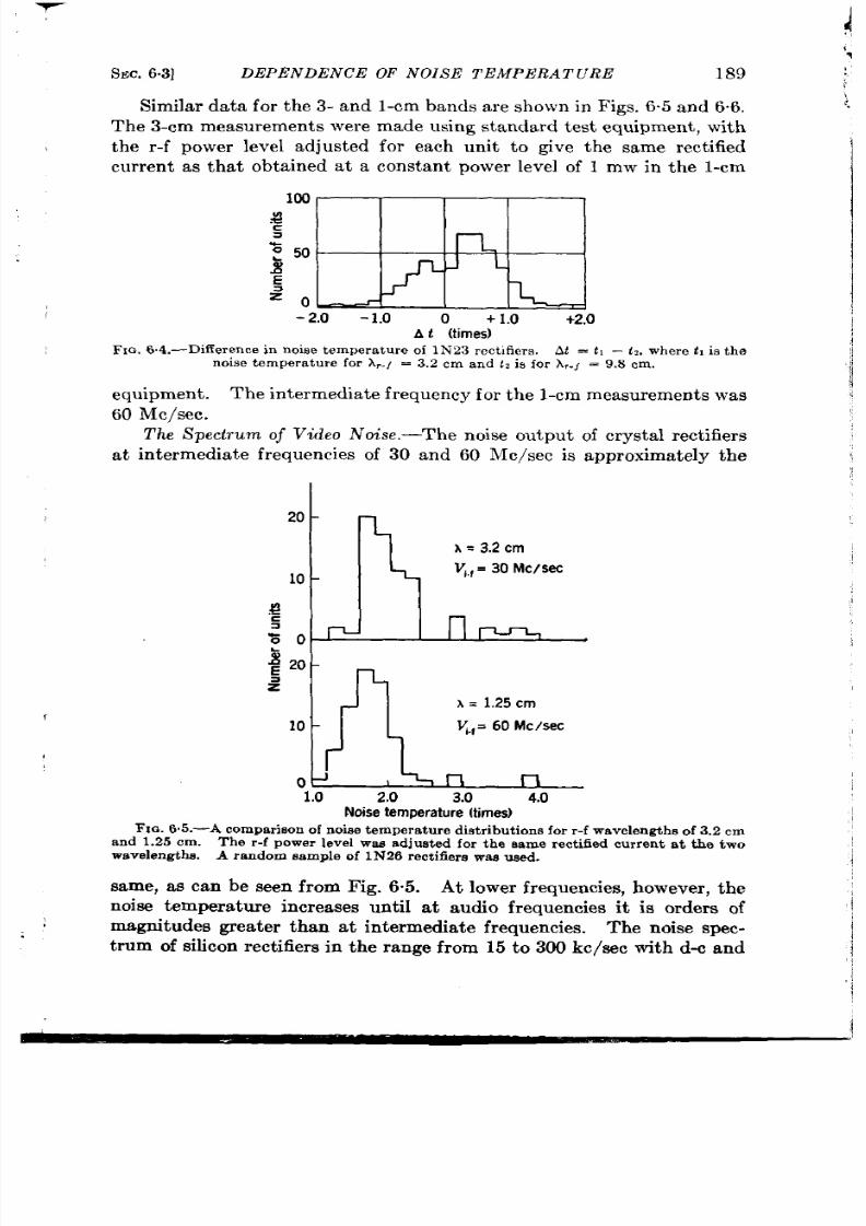
SEC.6.3]
DEPENDENCE OF NOISE T MPERATURE 189
Similar da ta for the 3- and l-cm bands a re shown in igs. 6.5 and 66.
The 3-cm measurements were made using standard test equipment , with
the r -f power level adjusted for each unit t o give the same rect ified
cur ren t as tha t obta ined at a const an t power level of I mw in the l-cm
‘ E
2.0 -1.0
0
+ Lo +2.0
At (times)
F IG. 6.4.—Differ en ce in n oise t emper a tu re of 1Nz3 r ect ifier s. At = t I – t ,, where tl is the
noise t em per at ur e for h,.I = 3.2 cm a nd LZs for X..f = 9.8 cm.
equipment . The in t ermechate fr equen t y f or the l-cm measurements was
60 Me/see .
!f%e
S pectrum of Video
Noise .—Th e n oise ou tpu t of cr yst al r ect ifier s
a t in termedia te frequencies of 30 and 60 Me/see is approxima tely the
20 -
A= 3.2cm
~,f= 30
Me/see
10 -
8
-
C
a
Zo
F
l-k-%
g 20 -
z
A= 1.25cm
10 -
V.,= 60 Me/see
0+
I
n
r -l
1.0
2.0 3.0
4.0
Noisetemper a turet imes )
FIG.6.5.—Acompa risonof noisetemper a tu re istr ibut ionsor r -f wavelengthsof 3.2 cm
and 1.25 cm . Th e r -f power level wa s a dju st ed for t he same r ect ified cu rr en t a t t he t wo
A r andom sample of 1N26 r ect ifier s wa s u sed .
same, as can be seen from Fig. 6.5.
At lower fr equ en cies, h owever , t he
noise tempera ture increases unt il a t audio frequencies it is orders of
magnitudes gr ea ter than a t in termedia te frequ encies.
The noise spec-
t rum of silicon rect ifier s in the range from 15 to 300 kc/see with d-c and

190
NOISE Gh’NEIiA TION
[SEC.63
r-f excita t ion has been invest igated by Miller et al.’ No data are avail-
able in the ran ge from 1 t o 30 Llc/sec.
A block diagram of t he appa rat us
and a circuit diagram of the input circuit used by Miller for the fr quency
~ 20 -
.=
a
%
# 10
r
z
o
n r -II-l
-2.0
-1.0
0
+1.0
+2.0
At (t imes)
FIc. 6.6.—Differ en ce in nois e t emper a tu r e of 1N26 r ect ifier s. At = t I —t~,wher e t l is
t he n oise t em per at ur e fo X,.f = 3,2 cm, u ;.f = 30 Me/see a nd tz is t he nois e t empera tu r e
for A,.f = 1.25 cm , u ;., = 60 Me/see.
Da ta a re for t h e ame unit s plot t ed in F ig. 6.5.
range from 15 to 300 kc/see are shown in Fig. 6.7. The dynamic
impeda nce I?z of t he cryst al, t he input r esist or
R 1, a nd t he load resist a nte
of t he diode
RD
are connected in para llel to the grid of the first amplifier
tube. The rest of the circuit is for applying d-c bias to the crysta l. The
Noise
diode
R~
=
Input circuit
To video
amplifier
NC 101X
communication
receiver
Local
oscillator
Block Oiagram
Fm. 6.7.—Inpu tcircuitand b lock d iagram of appa ra tu s for measur ingnois e t empera tu r e a t
low frequencies.
is given by Eq. (l).
1P. H . Miller , M. N. Lswis ,L. I. S&M, and W. E . S tephens,“Noise Spect rumof
Silicon Rectifiers,”NDRC 14256, Univ. of Penn., Mar. 20, 1944.
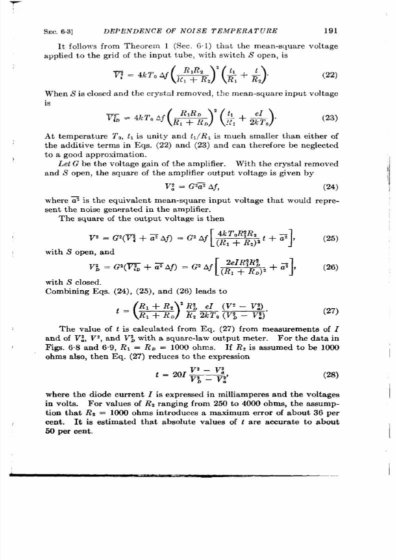
II
SEC.63]
DEPENDENCE OF NOISE TEMPERATURE 191
It follows from Theorem 1 (Sec. 6“1) that the mean-square voltage
applied to the gr id of the input tube, with switch S open, is
w=4 k ’ ’ 0 A - @%) 2 ( & ) ”
22)
When S’is closed and t he cr yst al r em oved, t he mean -squ ar e inpu t volt age
is
( “R” Y(2+&)” ’23)
WD ==4kT0 Af & + R.
At t emper at ur e To, t, is unity and tl/ R , is much smaller than eith r of
the addit ive terms in Eqs, (22) and (23) and can therefore be neglected
t o a good appr oximat ion .
\
Let G be the voltage gain of the amplifier . With the crysta l removed
i
and S open, the square of the amplifier output voltage is given by
V: = G2~
Af,
(24)
where ~ is the equiva lent mean-square input voltage that would repre-
sent th e noise gen era t ed in the amplifier .
The square of the output voltage is then
——
[
‘k TOR~Re —
1
2 = “(v: + a’ ‘f) = ‘2 ‘f
(R , + R ,)’ t + az ‘
(25)
with S open, and
wit h S closed.
Combhing Eqs. (24), (25), and (26) leads to
‘ = ( u 3 - -
R% eI (V’ – V:) .
R , 2kT0 (Vi – V:)
(27)
The value of t is ca lcula ted from Eq. (27) from measurements of 1
and of V~, V2, and V; with a square-law output meter . For the data in
Figs. 6.8 and 6 9,
RI =
R. 1000 ohnw. If
R* is
assumed to be 1000
ohms also, then Eq. (27) reduces to the expression
(28)
where the diode current Z is expressed in milliamperes and the voltages
For values of
RZ
ranging from 250 to 4000 ohms, the assump-
t ion that Rz = 1000 ohms int roduces a maximum er ror of about 36 per
cent . It is est imated that absolu te values of t a re accura te to about
50 per cent .
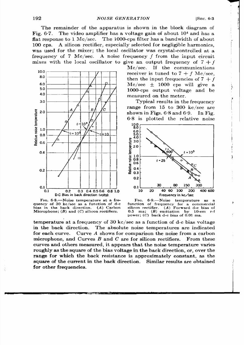
192
NOIS E GEN ERA T IOAI’
The remainder of the appara tus is shown
[SEC. 63
in the block diagram of
I?ig. 6.7. The video amplifier has a voltage gain of about 104 and has a
fla t esponse to 1 Me/see. The 1000-cps filter has a bandwidth of about
100 cps. A silicon r ect ifier , esp cia lly elect ed for n egligible h armon ics,
was used for the mixer ; the loca l oscilla tor was crysta l-cont rolled a t a
fr equency of 7 Me/see. A noise frequency j from the input circu it
mixes with the loca l oscilla tor to give an output frequency of 7 + f
10.0
8.0
6.0
5.0
4.0
3.0
2.0
1.0
0.8
0.6
0.4
0,2
0.1
0.1
0.2 0.3 0.40.50.6 0.S 1.0
DC Biasin backdirection(volts).
FIG. 68.-Noise tempera ture at a fre-
quency of 30 kc/see as a funct on of d-c
bias in the back direct ion . (A) Carbon
Microphone; (i?) and (C) s ihcon rect ilie ra .
-
Me/see. If the ~omrnunica t ions
receiver is tuned to 7 + ~ iVIc/see,
then the input frequencies of 7 + j
Me/see ~ 1000 cps will g ve a
1000-cps output voltage and be
measured on the meter .
Typica l results in the fr equency
range from 15 to 300 kc/see are
shown in Figs. 6.8 and 6.9. In Fig.
6.8 is plot ted the rela t ive noise
0.1
30
so 150 3W
10 20
4060 100 200 4CM3600
Frequency
n kcAc
FIG.
6.9.—Noise tempera ture as a
funct ion of fr equency for a commercia l
silicon rectifier. (A) F orwa rd d-c bla a of
0.5 ma;
(B )
excita t ion by 10-cm r -f
power ; (C) ba ck d-c bia s of 0.01 m a.
tempera ture a t a fr equency of 30 kc/see as a funct ion of d-c bias vol age
in the back direct ion . The absolu te noise tempera tu res ar indica ted
for ach urve. Curve
A
shows for compar ison the noise from a carbon
microphone, and Curves B and C are for silicon rect ifiers.
From these
curves and others measured, it appears tha t the noise tempera ture var ies
roughly as the square of the bias voltage in the back direct ion , or , over the
range for which the back resistance is approximately constant , as the
square of the current in the back direct ion . Similar resu lt s a re obta ined
for other fr equencies .

SW. 63]
DEPENDENCE OF NOISE TEMPERATURE 193
In F ig. 6.9, t he r ela tive n oise t em per at ur e of a silicon cr yst al is plot ted
as a funct ion of fr equency under the following condit ions: for Curve A,
a d-c forward biasing cu rren t of 0.5 ma, Curve 1?, excit a t ion by lo-cm r-f
power a t a level which gives a rect ified cu r ren t of 0.5 ma, and Curve C,
a back d-c biasing cur ren t of 0.01 ma.
Th e a ppr oxim at e a bsolu te va lu e
of the noise t empera tu res a re indica ted on the figu re for each curve.
This pa r t icu lar cryst a l has a noise tempera tu re of 1.6 a t 30 Me/see.
It is seen from the curve tha t (a ) the noise with back bias is many
t imes la rger than with forward bias, and (b) the noise t empera tu re var ies
inver sely as the fr equency for both d-c bias and r -f excit a t ion in the
fr equ en cy ra nge in vest iga ted. 1
This r ela t ionsh ip is typica l of all the
:
crysta l r ect ifier s measured by
iller , as well as for car bon micro-
f
phonesz and th in meta l r esistor s3
measu red by others. Miller and
Greenbla t t4 have a lso made meas-
u rement s in the audio range from
50 to 10,000 cps with an audio
amplifier and appropr ia t e filt er s.
In Fig. 6.10 is shown a typica l
n oise t emper at ur e-fr equ en cy cu rve
for a crysta l biased with 0.3 volt in
the back direct ion . It can be seen
from the cu rve tha t the inver se-
frequency law is va lid down to fre-
quencies as low as 50 cps. It was
a ls o found tha t in t h e audio-fr equen -
cy r ange t he n oise t emper at ur e with
d-c excit a t ion v r ies as the square
of the cu r ren t in the back dir ect ion ,
100
50
%
=
g 10
2
c
5
.-
al
~
s
~ 10
:
$ 0.5
g:
3
0.1
50 100
w lWO 10,OW
FrequencyinCPS
FIG.6.10.—Relativenoisetemperature
ofa siliconcrysta las a functionoffrequ ency
in th e audio-frequencyange,for a d-c bias
of 0.3 volt in th e back direction.
in a~reemen t with the resu lt s m-e-
viously given for the frequent y range from 15 to 300 kc/see.
Th e exper im en ta l difficu lt ies of mea su rin g n oise a t a udio fr equ en cies
make it difficu lt t o assign an absolu t e va lue to the noise tempera tu re;
for the cryst a l used in obta in ing Fig. 6.10 the value of the noise tempera -
tu re, ca lcu la t ed for a cr sta l r esist ance of 300 ohms, is about 14,000 at a
I In a pr iva te communica t ionto the authors Mille r s ta tes th a t unpublishedwork
in the W& to 1000-kc/secr ange indicatesthat the invercerelat ionshipis val id at lecst
to 1000kc/see.
3C. J . Chr is t ensenand G. L. Pea rcon , “F luctua t ions in Carbon Con tact s ,” Bell
S ystem Tech. J ., 16, 197 (1936).
8J . Bernamon t ,
“Fluctuat ions de Potent ia l d’un Conducteur Metal lique,” Ann.
phys ., Series 11, 7, 71 (1937).
4 P. H . Miller a nd M. H . Gr een bla tt , “Cr yst al Au dio Noise,” NDRC l~s87,
U . of P snn ., J an . 5, 1945.

194
NOIS E GENERAT ION
[SEC.64
frequency of 1000 cps. S nce theresistance ataback voltage of 0.3 volt
is probably of t he or der of sever al thousand ohms, th et rue n oise tempera -
turemay beasmuch a tent imes this value. Ext rapola t ion of the curve
of F ig. 6.8 to a requency of 1000 cps gives a noise tempera tu re of about
100,000 wit h a biasin g cu rr en t of 0.01 ma in the back direct ion.
Measurements made y the Pennsylvania group
on a
representative
sample of commercia l rect ifier s indicate that something like 5 per cen t
of the units tested have a noise tempera tu re at 1000 cps of less than 700,
for lo-cm excita t ion and 0.5 ma rect ified curren t .
Since both J ohnson noise and diode noise
are
independen t of fre-
quency, the large increase in noise observed at low fr equencies must
be the result of some other mechanism, one that could account for the
inverse dependence on frequency observed in the range from 50 cps to
0.5 Me/see. No adequate hypothes s for such a mechanism has as yet
been sugges ted .
6.4. Dependence on Temper tu re.-Lit t le is known about the way in
which noise tempera tu re var ies with the ambient temperature of the
rect ifier . It was seen in the ear lier par t of this chapter that the theory
of generat ion of diode noise in the crysta l bar r ier and J ohnson noise in the
spr eading r esist an ce pr edict s less n oise than is in most cases bserved
with d-c excita t ion. The mechanism of the genera t ion of the excess
noise is as yet unknown.
The only ata available a re measurements by Lawson, Miller , and
Stephens)l who used aluminum-doped silicon rect ifiers made in the
labora tory. With d-c excita t ion, measurements of the 30-Mc/sec noise
temperatu re wer e made at room and liquid-a ir tempera tures. A forward-
bias voltage was used and adjusted for each crysta l to give the same d-c
cur r nt a t the two temperatures; both the dynamic d-c resistance,
obtained from the slope of the character ist ic curve, and the spreading
resistance increase with decreasing temper at ur e, t he low-tempera tu re
bias therefore being always the larger . The crysta ls used were unfilled
in order to avoid changes ar ising from cont ract ion of the wax filler a t the
low temperature. The data listed in Table 6.1 are for those units that
su rvived a cooling cycle with less than 2 per cen t chan ge in noise t emper a-
tu re. The observed values of noise tempera tu re, in terms of the standard
temperatu re of 290°K, are listed in Column 7 of Table 6.1. The last
column lists the value calcula ted for diode and J ohnson noise alone; use
was made of Eq. (9) and the data for spreading resistance and bar r ier
r esist an ce obt ain ed fr om an a nalysis of t he d-c cu rve an d listed in Column s
5 and 6 of Table 6,1. It can be seen that a l hough the diode and J ohnson
n oise in gen er al decr ea se wit h decr ea sin g t emper at ur e, t he obser ved n oise
t emper at ur e does n ot sh ow a sign ifica nt t ren d in eit her dir ect ion ; i%wou ld
I A. W. Lawson,P. H. Miller , and W. E. Stephens ,“ Noisein Silicon Rect ifiersa t
Low Temperatu res,”NDRC 14-189,U. of Penn., Oct. 1, 1943.

SEC.65]
CRYSTAL AS A MICROWAVE NOIS E GENERATOR
195
TABLE6.1.—CALCULATEDNDOBSERVEDEPENDENCEFNOMETEMPERATUREN
crystal
1
2
3
4
5
6
7
8
9
10
?emperw
ture, “K
300
80
300
80
300
80
300
60
300
80
300
80
300
80
300
80
300
80
300
80
Bias
voltage,
volts
0.28
0.69
0.32
1.24
0.30
0.90
0.18
0.75
0.21
0.62
0,28
0.70
0.27
0.64
0.20
0,52
0.17
0.65
0,20
0.58
U31ENT1
D-c
wrrent ,
ma
0.77
0.77
0.77
0.77
0.77
0.77
0.58
0.58
0.60
0.58
0..59
0.59
0.58
0.56
0.58
0,58
0.58
0.58
0,58
0.58
fPERATU
Barrier
sistance,
ohms
35
70
60
50
60
90
60
160
50
120
105
85
60
0
45
50
30
90
40
40
>sistance
ohms
30
380
60
400
40
300
40
360
50
300
45
380
60
530
65
230
80
290
70
280
t
lbserved
2,1
1.7
6.8
6.4
9.0
5.4
1.7
3.2
1.6
1.8
2.1
1.9
3.0
2.3
2.7
2.7
2.6
2.0
1.5
(calcu-
mted for
[ohnson
nddiode
noise
only)
0.8
0.4
1.0
0.3
1.0
0.5
0.8
0.8
0,8
0.6
1.2
0.4
0.9
0.3
0.8
0.3
0.9
0.5
0.7
0,2
therefore appear tha t the excess noise for d-c excita t ion does not decrea se
as the tempera tu re drops. As yet no invest iga t ion of th is efiect has been
made wit h r -f excit at ion .
MICROWAVE NOISE
6.5. The Crystal as a Microwave Noise Genera tor .-There is lit t le
quant itat ive informat ion on crysta l-noi e genera t ion at microwave fre-
quencies.
What informat ion is available concerns the use of the crysta l
rect ifier with d-c excita t ion as a microwave noise sour ce for noisdi~e
measurements.
In th is applicat ion t he available n oise power u nder gken

196
N IS E GENERA T ION
[SEC.
6.5
condit ions of excita t ion must be known; this power may be expressed
conven ien t ly in terms of the noise tempera ture a t the specified radio
fr equency. As a noise source, the crysta l is placed in a convent iona l
crysta l holder such as is used for mixer -crysta l test ing. The d-c bias is
applied a t the i-f termina ls of the mixer and the r -f noise power is then
availab e a t the r -f termina ls. The incoherence of the instantaneous
noise voltages makes matching the crysta l to the r -f line with conven t iona l
r -f t r ansforming devices difficu lt , bu t crysta ls tha t ma tch approxima tely
in the standard holder s can be chosen from commercia l product ion . If
4
+
1
3
(a) Magic-T
II
O
Attenuator
Filter
4
‘+ %=--L&J
Matched
load
dl
Attenuator
Noise
ctystal
b
M
(b)
output
meter
F IG. 6,11.—Appar a tu s for mea su r ing t h e r -f nois e t emper a t ur e of a cr yst a l r ect ifier .
the crysta l is misma tched, 5 t o 10 db of a t ten ua tion can be pla ced bet ween
it and the r -f ou tpu t terminals whenever it is desired tha t the noise-
gen era tor impedance be the character ist ic i pedance of the r -f line. The
measured noise tempera tu re in the mismatched case, however , will be
less than the t rue va lue since not a ll of the available ou tpu t noise power
will be mea su r ed .
Like low-frequ en cy n oise, th e micr owa ve n oise power ou tpu t is mu ch
la rger with d-c bias in the back direct ion ra ther than in the forward
direct ion . With a bias cur ren t of 3 to 4 ma in the back direct ion , the
3-cm noise tempera tu re of a random sample of 1N23 rysta ls lies in the
range from twen ty-five to for ty t imes; the r -f noise tempera tu re of 1N26
crysta ls a t 1.25 cm lies in the range of about ten to twen ty t imes.
On e
method of measur ing the r -f noise tempera tu re ut ilizes the “magic T’, ”
shown in Fig. 6.11. The proper t ies of th is device are discussed in deta il in
Vol. 16 of the Radia t i n Labora tory Ser ies; the par t icula r proper ty of

SEC.
6.5]
CRYSTAL AS A MICROWAVE NOISE GENERATOR 197
in terest in th is applica t ion is that when Arms 1 and2 are termina ted with
matching loads, Arms 3 and 4 a re completely decoupled. In the appara tus
shown in Fig. 6.11 the loca l oscilla tor is connected to Arm 4, and the crysta l
to be tested to Arm 3; loca l-oscilla tor power therefore does not en ter the
noise-crysta l circu it . Half of the output power of the crysta l is absorbed
in the matched load in Arm 1, but this is compensa ted for by the fact
tha t both noise sidebands are conver ted to in termedia te frequency by the
mixer . The i-f output termina ls are connected to an i-f amplifier and
output meter . A noise diode, not shown in the figure, may be connect ed
to the input termina ls of the i-f amplifier for ca libra t ing the output meter .
The measurement consist s essent ia l y in ascer ta in ing two quant it ies:
(1) The noise tempera ture t= of the mixer crysta l with the noise source
replaced by a ma tched load. This is preferable to turn ing off the noise
source since the r -f impedance of the noise crysta l changes markedly with
d-c bias. (2) The noise tempera ture of the mixer crysta l t : with the
noise source on. In the la t ter case the available noise ower a t the
input terminals of the i-f amplifier will be
N~ = kT& Af + kTotG. Af,
(29)
where
t k
the r -f noise tempera ture to be measured and G= is the con-
version gain of the mixer crysta l.
The fir st term of the r ight -hand
member is the available noise power from the mixer crysta l and the
second term is the conver t ed noise power from the noise crysta l.
The
noise t empera tu re t : s then
N,
‘L = kT ,
Af
=
t,+
tGz,
(30)
fr om wh ich
t;– t.
t=—
G= “
(31)
The measurement of t :, t ., and G. is accomplished by the methods
discussed in Chap. 7. The standard noise set descr ibed in Chap. 9 can
be convenien t ly used by connect ing its mixer to Arm 2 of the magic T of
F ig. 6.11.
This method may also be used for the ca libra t ion of a noise source
employing a reflex velocity-modula ted tube, s ch as tha t descr ibed in
Sec. 7.11.
Alterna t ively, the r -f oise power from the noise crysta l may be
mea sured with the microwave radiometer repor ted by Dicke. 1 This
inst rumen t is escr ibed in Vol. 24, Chap. 5 of the Radia t ion Labora tory
Ser ies. This method has been used to ca libra te l-cm crysta l noise
sou r ces for u se in noise-figu r e mea su remen ts.
I R. H. Dicke, “The h fea su rem en t of Th erma l Ra dia tion at Micr owa ve F requ en -
cies,” RL Repor t No. 787, Aug. 22, 1945.
.

CHAPTER 7
LOSS AND NOISE MEASUREMENTS
LOSS MEASUREMENTS
7.1. Genera l Considera t ions.-The in it ia l sect ions of th is chapter
t rea t the problem of conver sion loss measu rement . A difficu lty ar ises
from the need for appara tus tha t will sa t isfy two incompatible requ ire-
ments.
F irst , t here is needed for the research labora tory an appara tus
tha t can measure conversion loss under genera l tuning condit ions in
order proper ly to evalua te the capabilit ies of exper imenta l crysta ls.
Th e flexibilit y deman ded of su ch a n a ppa ra tu s en ta ils u sin g a mult iplicit y
of con t rol knobs. They become even more numerous when facilit ies a re
provided for noise-tempera ture m asurements to eva lua te the over-a ll
per formances of the crysta ls under the same condit ions tha t obta in for
conversion-loss measurements .
Second, the appara tus must at the same t ime be simple enough for
m an ipu lat ion by un skilled per son nel in a ccept an ce t est in g of pr odu ct ion
units; in other words, it should have a minimum of cont rol knobs. But
here another problcm is encoun tered. Since the measurements must be
standardized, a uniform method of measu rement must be devised tha t
makes it possible for va lues obta ined at one stat ion to be reproduced at
another . In addit ion, measur ing condit ions should as far as possible
simula te those prevailing in system receivers.
But since the la t ter
condit ions va ry so much from one system to another , it is impossible to
sat isfy th is requiremen t and at the same t ime achieve uniformity and
simplicity. Conversion loss, as we have seen in Chap. 5, depends on the
in terna l impedance of the signal source and not only on the value of th is
impedance at signal frequency but a lso on its va lue a t image frequency
a nd, t o some xt en t, a t h armon ic fr equ en cies.
Now it happens tha t some
system receiver s a re designed to match the mixer to both input (signal)
and outpu t (i-f) circu its while other are designed to match the input
but to mismatch the output circu it in order to Improve the noise figure
of the amplifier . The terminat ion at in termedia te frequency does not
direct ly affect conversion 10SS, but , t ransformed th rough the mixer , it
a ffects the signal impedance of the rn ixcr and t!lus i,lm mat. h ing signal
source impedance on which the conversion loss depends.
Agiliu j some
systems are provided with broadband Tlt tubes ~~”hiclldo not rchct ’ the
I The sameresult is sometimesacbicvcd ill bdanccd mixerswith narrow-baudTR
tubes by t ak in g advan ta ge of t h e ph aw select ive p roper ties of t h e magic T or it s
coaxial equivalent [seeMicrowav e M iz crs, Vol. 16, Radiation I,?bo~atorySeries).
198
T
SEC. 7.1]
GENERAL CONS IDERATIONS 199
I
image frequency; other systems have sharply resonant TR tubes which
r eflect m ost of t he ima ge fr equ en cy power .
Fu rt hermor e, t he la tt er ca se
shows in pract ice a dist ressing lack of un iformity in the phase of the
reflected image wave. Fina lly,, some, but not a ll, system esigners have
in cor por ated h armonic filt ers in th e r -f circu it in or der t o t ake a dva nta ge
of harmon ic rein forcement . As a resu lt of th is lack of un iformity in
system design , two crysta ls of the same conversion loss in one receiver
may have differen t conversion losses in another . Actua lly such differ -
ences a re not l kely to exceed one or two decibels and a re not very ser ious
from the poin t of view of system efficiency. From the crysta l manu-
fa ct ur er ’s poin t of view, h owever , a differ en ce of on e decibel bet ween t wo
measur in g sta t ions is a ser ious ma tter .
F ailu re t o m eet t he con ver sion -
10SSt est specifica tio limit a s t est ed by t he st an da rd a ppa ra tu s ma y for ce
the manufactu rer t o r eject a sizable fract ion of h is crysta l product ion .
These reject ed unit s, however , may actua lly have less conversion loss
than some of the accepted unit s in some par t icu lar system receiver .
There does not appear to be any simple way ou t of th is dilemma.
Th e compr om ise fin ally a dopt ed in volves t he mea su remen t for pr odu ct ion
test ing of tha t pa r t icu la r va lue of the conver sion loss denoted in Chap. 5
by LO. This va lue is defined as the onver sion loss when the sourc
impedance is the same at both signa l and image frequency and is chosen
t o match the loca l-oscilla t r power (r a ther than the signa l power ) to the
mixer . We saw in Chap. 5 tha t in pract ice LO differs insignificant ly from
L,, the loss when the impedances to signa l and image a re equal, and th is
common impedance is adjust d to make the loss a minimum. As
expla ined in Sec. 5.6, LOis a lways grea t er than t e convers on loss mini-
mized in dependent ly, bot h with r espect t o t he signal impeda nce and with
respect to the image impedance.
Thus the system designer is a ssured
tha t a crysta l sa t isfying the t est specifica t ion limit on LOwill have a loss
less than or equal t o this limit in a well-designed receiver with either a
sharply or a broadly tuned r -f circu it .
The amount by which
LO
exceeds
the system receiver loss for the same crysta l will va ry in pract ice from
zero to about two decibels, t he amount depends on the cryst a l and on the
rece ive r des ign .
The measurement of LO can be made with a simple appara tus tha t is
r eadily a ligned and standardized and gives remarkably uniform result s.
This method is descr ibed fu lly in Sec. 7.4 and the st anda rdized test set
u t ilizing th is met hod is descr ibed in Sees. 9.1, 9.2, and 9.3.
No sign al in t he or din ar y sen se is em ployed in t his simplified mea su re-
ment .
It s fun ct ion is simula ted by a var ia t ion in loca l-oscilla tor power .
This var ia t ion may take the form of an incrementa l change in power or of
a n amplit ude modu la tion of t he loca l-oscilla tor wa ve.
Befor e discussing th e simplified meth od we shall t r ea t ot her met hods

200
LOSS AND NOISE MEASUREMENTS
[SEC.72
more su ited to the resea rch labora tory, namely the convent ional hetero-
dyne method (Sec. 7.2) and the impedance method (Sec. 7.3). These
have the advantage over the simplified metho of grea ter flexibility,
r .laking it possible to study conversion loss as a funct ion of image-
t un in g a nd ot her pa ramet er s.
Conversion loss may be determined indirect ly by measur ing the ele-
ments of the mixer admit tance matr ix.
As expla ined in Chap. 5, th is
ca n be a ccomplish ed by mea su rin g t he oca l-oscilla tor m ixer a dm it ta nce y,
the direct cu r ren t io, their der iva t ives with respect to absorbed loca l-
oscilla tor power P, and the direct volt age V. Although this method is
tedious and suitable on ly to the resea rch labora tory, it is very genera l,
giving not on ly the conversion loss with arbit ra ry image-tuning but a lso
the mixer admit tances. It a lso determines the exten t of reciprocity
fa ilure and t her efor e th e loss wh en th e m xer is u sed as a modu la tor ra th er
than as a demodula tor . (See Sees. 5.3 to 5.9, for deta ils.)
7.2. The Heterodyne Method.-The most obvious and direct method
of l ss measurement is the heterody e method. This method is some-
Fl
p k i = t i = l
FIG.71.-Block diagramof appara tusfor the heterodymemethodof 10SSmeasuremel,t .
I
t imes sa id to be the on ly rea lly reliable one since it is the on ly one tha t
simula tes system receiver condit ions. Actua lly, as we have seen in the
preceding sect ion , the simula t ion is a t best imperfect because of the
va r iety of condit ions one meets in system receiver s.
We must rea lize
tha t in any direct measurement of loss the va lue obta ined appl es only
to the specia l circumstances of the measurement .
The appara tus used in the heterodyne method of loss measurement ,
reduced to bare essent ia ls, is shown schemat ica lly y in Fig. 7.1.
A signa l genera tor feeds igna l power to the mixer wh ich conver t s
the power to the
“in termedia te fr equency” by bea t ing with the loca l
oscilla tor fr equency. The conver ted power is then measured with an
i-f wa t tr n et er .
Both the ava ilable power from the signa l genera tor a t .4
and the available in termedia te fr equency power at 1? must be measured,
their ra t io being the conversion loss. The available signa l power is a
.,
.
SEC.7.2]
THE HE TERODYNE METHOD
201
proper ty on ly of the appara tus and not of th e crysta l to be measured;
once it is determined it needs to be remeasured only occasionally as a
check on the constancy of the signal genera tor .
The mixer must be approximately matched to the i-f wa t tmeter since
the available i-f power is desired.
On the other hand, th e available
signal power is independen t of the tun ing at the r -f termina ls. This tun-
ing can be adjusted so tha t the measured loss con forms to the var ious
pecia l cases t r ea ted in Chap. 5.
The signal powe available a t A should be in the range of 1 to 10 pw
for best resu lt s. A power h igher than this leads to t rouble from non-
linea r ity since the mixer is linear on ly wh n the signal power is small
compared with the local oscilla tor power ( = 1 mw). Signal power less
than 1 pw is difficu lt to measure accura tely. The power available a t A
may be measured by breaking the connect ion at A and feeding the signal
in to a n r -f wa ttmet er (bolom et er ).
If th is is not available as a standard
piece of t est equipment , it can be easily const ructed. A thermistor
elemen t such as a Wollaston wire or a Western Elect r ic bead thermistor
is used as one arm of a d c br idge.
The br idge is ba lanced with no r-f
powe a pplied t o th e sen sit ive elem en t.
Aft er a pplica t ion of r -f power ,
ba la nce is r est or ed by decr ea sin g t he dir ect -cu rr en t power in t he sen sit ive
elemen t . The r-f power is then just equal to the difference in d-c power .
Care must be taken to insu re a good r -f match to the sensit ive elemen t .
The in termedia te-frequency wat tmeter may be a bolometer of a
similar na tu re. Because a con t inuous indica t ion is desirable for rapid
measurement , i is conven ien t to c libra te the i-f wa t tmeter in terms of
the off ba lance indica t ion of the br idge. For accura te measurement a
good match from the mixer to the i-f wa t tmeter is desirable.
As an alt erna t ive to the i-f bolometer , an amplifier followed by a
calibra ted (preferably square-law) detector may be used as a wat tmeter .
Such a detector as the advan tage of being free from undesirable thermal
effect s. It is not easy, however , to mainta in a constan t amplifier ga in a t
usual in termedia te frequencies ( =
30 Me/see), a lthough the difficulty
is much reduced if the in termedia te frequency is in the audio range.
But then the problem ar ises of mainta in ing the two h igh-frequency
oscilla tor s a t a sma ll fr equ en cy sepa ra tion .
One solu t ion is to use on ly
on e oscilla tor wit h a udio-fr equ en t y amplit ude modu la tion (see Sec. 7“4).
The two modula t ion sidebands then replace the signal. This method
has the disadvantage that no discriminat ion b tween signal and image is
p ssible, with the resu lt tha t the l ss can be measured on ly under the
condit ion of equal impedance at signal and image.
The i-f amplifier ga in can be mainta ined at some constan t level by
making frequen t reference measurements of “standard crysta ls. ” Main-
ta in ing gain by this method is difficu lt if var iable tuned measurements

202
LOSS AND NOISE MEASUREMENTS
[SEC.73
a re wan ted, because it means retu rn ing to some standard tune each t ime
a check measurement is made.
Th er e is n o such difficu lty with fixed-tu ned mea surem ents, fo which
the mixer is permanen t ly t ned at input and ou tput a t some standard
impedance level. This level is determined by fin ing the mean of th
impedance spreads of a la rge number of crysta ls of the type to be
measured. The circumstance tha t the actua l absorbed i-f power ra ther
than t he available power is mea su red, h owever , in tr oduces er ror .
In the heterodyne method one must take ca re to maintain frequency
The usual AFC techniques can be employed to
main ta in con st an t fr equ en cy dif er en ce.
If h ighly reson ant r -f circu it s
a re to be used, however , absolu te frequency stability shou ld be main-
ta in ed. A sat isfa ctory meth od is to u se on e of th e frequ en cy stabilizat ion
schemes d vised by Pound (see Vol. 16 of the Radia t ion Labora tory
Series).
To study conversion 10s9 as a funct ion of image impedance, a filter
must be used in the signal genera tor lead. A high-Q tr nsmission cavity
such as a TR tube might , for example, be inser t ed a t A in Fig. 7.1. The
phase of the image wave reflected by the cavity can then be a ltered by a
line st r etcher between the mixer and the cavity. P roper account must
be taken of the signal t ransmission loss in the cavity. A difficu lty
encoun tered in such an arrangement is tha t oca l-oscilla tor power is a lso
reflected by such a bandpass filter , and large var ia t ions in rect ified
crysta l cu r ren t occur when the phase of the reflected image wave is
a ltered by the line st ret cher . A more sa t isfactory method is to use a
band-reject ion filter tha t r eflect s on ly the image frequen t y; a sidearm
can be a t tached at A (Fig. 7“1) and termin ated by a sin gle window ca vity
tuned to the image frequency. The line length between th i cavity
and the main line is then adjusted to pass an off-resonan t frequen t y
th rough he main line without reflect ion while the image frequency is
reflected. The phase of the reflected image wave can then be var ied by
adjust ing the line length between th is sidearm and the mixer .
A device
of th is type was employed by Be r inger (see Sec. 7“7) in his invest iga t ion
of the effect of image impedance on loss and noise tempera tu re.
7.3. Impedance Methods.-I is well known tha t the transmission
loss of a four-terminal linea r passive network can be etermined from a
number of measurements of the impedance at one terminal pa ir with
known loads a t tached to the opposite pair . Any linear four-terminal
device is completely specified by its admit ta nce m atr ix, th at s, by t he t wo
self-a dm it ta nces a nd t he two t ra nsfer a dm it ta nces.
If the device is pas-
sive the two transfer admit tances a re equal and give reciprocity. In such
a device on ly t hr ee (complex) qu an tit ies a re n eeded t o defin e t he pr oper ties
o’ the device; the loss may be measured y not more than th ree independ-
1
SEC.7-3]
IMPEDAN CE METHODS
203
en t measurements of impedance. If r eciprocity does not hold, h owever ,
the four character ist ic pa rameter s determin ing the proper ties of the net -
wor k ca nn ot all be det ermin ed by impeda nce m ea su rem en ts.
The r ea son
is that impedance measurements determine only the product of the t rans-
fer admit tances whereas the loss depends on their ra t io a lso.
We have seen (Chap. 5) tha t a crysta l mixer can be regarded aa a
linear network which, however , is not genera lly passive. The con-
ver sion loss of the mixer cannot ther efor e be determined in genera l by
impedance meas rements a lone. Reciprocity fa ilure has so fa r been
obser ved only in germ an ium r ect ifier s, h owever ; t he impedan ce m et hod
can st ill be used, t her efor e, for silicon crysta ls, a lt hough n ot with per fect
confidence. The impedance method is wor th using when possible
because the method is easy, quick, and capable of high precision .
If a t least weak reciprocity (equality in phase of the t ransfe admit -
t an ces) ca n be gen er ally a ssumed, a nd n o except ion h as yet been obser ved,
the impedance method st ill has some genera l u t ility. As noted in Sec. 5.8,
if wea k r ecipr ocit y h olds, con ver sion loss L can b expressed as
(1)
where gcfl/gBa ,t he so-ca lled f‘r ecip rocit yy fact or , ” is t he r a t io of t he signal–
i-f t o t he i-f–sign al t ra nsfer a dm it ta nce.
Th e qu an tit y
L’,
the so-called
“impedance loss,” depends only on the product of gefl and g~~,not on the
ra t io, and can th refore be determined by impedance measurements.
Thus by measur ing the dependence of L’ on image-t uning in this way, t he
va ria tion of L with image im edance can be determined at least t o with in
a con st an t fa ct or .
An ear ly pplica t ion of the impedance method to crysta l mi ers was
made by Marcum, 1 who measured r -f impedance with open-circu it ed and
close -cir cu it ed i-f t ermin als.
Dicke2 also devised a version of the
impedance method involving the measurement of i-f impedance with
th r ee different r -f loads.
Later R. V. Pound modified and improved
Ma r cum’s met hod.
Th e Dicke ikfet hod.-Tbis m et hod has t he a dvantages of being simple,
quick, and capable of high precision . F igure 7.2 shows a block &gram
of the appara tus used.
An r -f oscilla tor buffered by a matched a t t enua tor feeds a slot t ed
sect ion of waveguide into which may be inser t ed a standard susceptance
consist ing of a meta l wire encased in a polystyrene plug. The slot t ed
1 J . I. Ma rcum, ‘(Oper at ion of Cr yst al Rect ifier U nit s a t Micr owa ve F requ en cies, ”
Wes tin ghou se Resea r ch Repor t SR-158,. Dec. 4, 1942.
2 R. H. Dicke, Reciprocity Theorem and Its Applica t ion to Measu remen t of
Ga in of Micr o-Wa ve Cr yst ai Mixer s, ” RL Repor t N o. 61-18, Apr . 13, 1943.

I
204
LOSS AND NOIS E MEASUREMENTS
sect ion is followed by a line st r et cher whose purpose
[SEC.73
f
is to va ry the
elect r ica l distance between th e susceptance and the crysta l. Next comes
the crysta l mixer , provided with a tuner for match ing it to th e wave-
guide.
Th e d-c term ina ls of t he m ixer wh ich also ser ve as t he i-f term ina ls
a re conn ected to a 60-cps br idge.
Th e m ea su rin g pr ocedu re is a s follows:
1. The mixer is ma tched to the gu ide and the r-f power is either
adjusted to some standard va lue or adjusted to give the desired
r ect ified cu r r en t .
The r -j
power is
abou t 1 mw (ordina ry loca l
oscil lator level).
Oscillator
~ q
Standard
Suaceptarrca
Attenuator
slotted
Line
section
stretcher
1
t
I
60.cps
—
crystal
bridge
—
Tuner
mixer
FIG. 7.2.—B1ock d iagram for the Dicke impedance method of los s measu remen t .
2. The dynamic conductance of the mixer a t 60 cps is measured with
the br idge. This quant ity we denote by go.
3. The standard susceptance is placed in the slot t ed sect ion and the
a t tenua tor adjusted to give th e or igina l crysta l cu r ren t .
4. Th e line st ret ch er is adju st ed t o maximize t he 60-cps con du cta nce.
This va lue gl of the conductance is measured.
5. Th e line st r et cher is adjusted to minimize the 60-cps conductance.
This minimum con du ct an ce g~ is m easu red.
The (impedance) conversion loss may then be found from these data ,
gO, gl, and gz, together with the va lue P of the standing-~vave voltage
ra t io in t roduced in th e gu ide by the standard susceptance.
In par t icu lar th e va lue of L& the impe ance conversion loss when
image and signal a re termina ted a like and the mixer is ma tched a t local-
oscilla tor level, is given by
14=2p~
90(91 – 92)
(2)
,0 + 1 (91 — go)(90 — g:)”

SEC.73]
IMPEDANCE METHODS 205
Equa t ion (2) will be der ived no~v, and it will be shown how the con .
version loss under other condit ions of tun ing may be determined from
the same data .
Equa t ion (5.64) gives the i-f conductance ge of the mixer when the
r-f load admit tance common to signal and image is a rea l conductance go.
If th e r -f load admit tance is not purely rea l, th e i-f admit t nce remains
rea l provided the r -f dmit tance is th e same a t signal and image.
Using
an analysis similar to tha t employed in der iving Eq. (5”64) we find for
gej in th is m ore genera l case,
29.690.(9..
– (7.7 + 9.)
‘d = ‘BP–
(g=. + 9.)’ + b: – 9:,’
(3)
where
y. = g.a+ jba
(4)
is the r -f load admit tance.
Equa- .~ba
tion is easily seen to reduce to
Eq. (5.64) if we pu t b= = O. Now if
t he stan da rd su scepta nce is in ser ted
and the line is st ret ched between the
susceptance and the crysta l, th e r -f
Pf l
load admit tance y. will t r aver se a
v=
cir cle in t he a dm it ta nce pla ne.
This
circle has it s cen ter on the rea l axis
which it in tersects a t g= =
pg
and
1
g. = ~ g, where g is the gu ide con -
FIG. 7,3.—Diagram showing circle
ductance and p t h e st a nding-wave
t rave r sedby the r -f load admit t anceas
thelineisstretched:u = lineconductance;
volt age r at io in tr odu ced by in ser tin g
p = stan ding-wave rat io.
the susceptance (see Fig. 7“3). Tbe equat ion of the cir cle is
(5)
If Eq. (5) is solved for
ba
and subst itu ted in Eq. (3), we see tha t th e resu lt -
ing expression for gp can be expressed as a fract ion conta in ing g. linear ly
in both numera tor and denomina tor .
Consequen t ly gfl as a funct ion of
go has no sta t iona ry va lues, and the grea test and least va lues of g8 occu r
a t the ext reme values of ga , tha t is, a t g. = pg and g. = g/P . Fur ther -
more, b. = O at both these poin ts.
Thus we obta in from Eq. (3) for
gl and g, respect ively the maximum and minimum values of g~ as the l ne
is s t r et ched,
2g=pgfla
g,
=
g~p
–
9.. + 9., +
P9’
2g=&7@.
g2 = g88 –
ff.. + 9.. + ff/P’
206
LOSS AND NOISE MEA SUIrW.t[llK 7’S [SEC, 73
Th e i-f con du ct an ce g,,, ~vh en t he st an dar d su sc pt an ce is r emoved, is
fou nd by r epla cin g p by nity in either of these result s,
(8)
Because, under this condit ion , the mixer is matched to the oscilla tor
conductance g, we have from ~q. (5.26),
g = g.. – g.,.
Equations (6) to (9) inclusive may now
g.~g~. wit h t he r esu lt s
9. R=; (P– I)MC
p-c~’
(9)
be solved for g==, g~p, and
(lo)
Ck+ 1)
(JBR= go + (gl – gJ
(p – cj(l + c}’
(11)
C(pz — 1)
g.pgb = (71 –
d 2(P _ ~)29!
(12)
~ ~ 91 – (41,
go – gz
(13)
Equat ions (9) to (13) inclusive give the elements of the admit tance matr ix
of the mixer in terms of the guide conductance g, the standing-wave
ratio
p,
and simple impedance measurements at the d-c erminals of the
mixer . Only th e product gaBgP.is determin ed in ‘his way. As ment ioned
above, the ra t io g.P/gPa—the reciprocity factor—cannot be found by
impedance measurements. Subst itu t ing these result s in to our formula
(Eq. (577)) for the conversion loss LOwe obtsin
LO=294F8P-1
(/0(91– 92)
96.
P + 1 (m – 90)070 – 92)’
(14)
which with Eq. (1) gives Eq. (2) for the impedance loss, L:.
The values obta ined for gaa, etc., may now be subst itu ted in to Eqs.
(5. 141) and (5. 142) to give the losses under various condit ions of image
tuning.
The grea t advantage of impedance methods is that no difficu lt
r -f power measurements ar e requ ired, wherea s all oth er methods involve
measurement of r -f power . This suggests tha t the impedance technique
may be used to measure r -f power instead of loss. For example Eq. (51),
which is der ived in the next sect ion , gives LO in terms of the r -f power P.
Eliminat ing Lo between Eqs. (14) and (51), a result is obta ined for P in
t erms of t he r ecipr ocit y fa ct or p an d of qua ntit ies all det ermin ed by simple
low-frequ ency measurements, capable of h igh precision . Of cour se, fu ll
reciprocity (gaP = g~a) must be assumed in such measurements, but th is

1
I
I
,
t
SEC.73] IMPEDANCE METHODS
207
assumption appears to hold for silicon crysta ls. This method of r -f
power measurement , suggested by Dicke, has not yet been exploited but
appears to have some valu . To the authors’ knowledge all other abso-
lute power measurements ar e ca lor imetr ic, that is, they involve the trans-
format ion o r-f power in to heat .
A specia l cas~ of in ter est ar ises wh en t he st an din g-wave volt age r at io p
becomes very large. In th is case gl and gz are the i-f conductance when
the r -f terminals are respect ively short -circu ited and open -circu ited.
From Eqs. (6) and (7) we find for
p = m ,
Q=l–
2g.Bgb.
gl
9.W(9.. + 9.7)’
(15)
Now in Sec. 57 it was shown that the loss La (loss m in im ized wit h r espect
to the r -f load impedance, which is the same at signal and image) is given
by Eq. (5.72)
(16)
9@-vl-?12
where q~ is given by 13q. (5.73). Compar ing thk expression for q, with
Eq. (15) we see tha t
L2.@d+ml.
9@ 1 – dg2/gl
(17)
Thus the (impedance) lOSSL; may be found from only two measure-
m en ts of i-f con du ct an ce, t he th ir d mea su rem en t (gO) bein g u nn ecessa ry.
In pr act ice t he oscilla tor power in
th is method is in t roduced in to the
guide by a loosely coupled probe,
and the impedance is changed
from a shor t circuit to an open
circuit by the mot ion of a plunger
terminat ing th e waveguide. This
method was suggested by F. B.
Llewellyn and has been used to
some ext en t at t he Bell Teleph on e
Labora tor ies. It has the disad-
va nta ge of r equ ir in g an oscilla tor
capable of putt ing out a large
amount of power , since the oscil-
la tor must be loosely coupled to
t he gu ide.
Also it is difficu lt to
keep the absorbed loca l-oscilla tor
t
Tuner Mixer
1L
1)
l-f
Local
terrninala
oadllator
F IG. 7.4.—Essen tia ls of t he Pound met hod
of 10ssmeasurement .
power constant as the plunger is moved. Fur thermore, the method
determines only 2 and gives no informat ion about the loss under more
gen er al condit ion s of t un in g.

208
LOSS AND NOISE MEASUREMENTS [SEC.73
T he Pou nd M eth od .—T he im peda nce con ver sion loss m ay equ ally WC1l
be determined from r-f impedance data . The essent ia ls of the Pound
method are illust ra ted in Fig. 7 “4.
An r -f br idge is connected to the
signal terminals of the mixer .
W th t he i-f terminals shor t-cir cuited,
t he t uner T is adjusted to balance the br idge. This opera t ion is equiv-
a lent to matching the mixer to the br idge circuit with the result tha t the
mixer does not reflect signal power .
The i-f terminals a re then open
~–~
t
t t
2
/
3
Magic T
R.f
Tuner
Mixer
shutter A
1
m
I
Matched t4atched
I
Signal
If
—
load
attenuator
generator
terminator
F IG .7 .5a .—B1ock d iagr am of appar a tw used in t h e Pound method of los s mea su r emen t .
Re.e;t:
meter
+
Mixer
1/
,
I
=
=
FIG.7.~.—Diagr8mof the i-f circuitin the Poundmethodof loaameasurement.
cir cu it ed a nd t he off-ba la nce r ea din g of t he ba la nce in dica tor is r ecor ded.
The (impedance) conversion loss is then direct ly obta ined from this one
datum.
A more deta iled diagram of Pound’s appara tus is shown in Fig. 7.5.
The test mixer is mixer A and the r -f br idge is the magic T with it s
associa ted circuit in Arms 1, 2, and 4. There is no direct cross coupling
between opposit e arms of the magic T. Thus if &ms 3 and 4 are termi-
nated in matched loads, no power from the signal genera tor will go up
Arm 2, the indica t ing arm of the br idge, and the balance-indica t ing
SEC. 7.3]
IMPEDANCE METHODS
209
meter M will read zero If Arm 3 is mismatched, half the signal power
reflected by Arm 3 goes up Arm z and the other half is absorbed in Arm 1.
The reading of meter M is therefore propor t ional to the signal power
reflected by Arm 3.
The crysta l t o be tested is placed in mixer A and the procedure is as
follows:
1.
2.
3.
4.
The power of t he local oscilla or A is adjusted to give the desired
crys ta l cu r ren t .
Th e i-f t ermina ls a re sh or t-cir cu it ed (Swit ch Posit ion 1 in F ig. 7.5b
and the tuner T is adjusted unt il met er M reads zero. This
matches the signal t o the mixer .
The i-f t ermina t ion is switched to a para llel t ned circuit (Switch
Posit ion 2 in Fig. 7.5b) and the circuit is tuned with the variable
condenser for maximum reflected signal power as indica ted by
meter M. As will b shown la ter , this opera t ion is equivalent t o
open -cir cu it in g t h e i-f t ermin als.
The conversion loss is then given by the formula
(18)
The loss given by Eq. (18) is tha t obta ined when the interna l imped-
anc of the signal source is adjusted to make the loss a minimum.
Th e
image termina t ion is held fixed in making this adjustment . In Eq. (18)
g.~/g~. is the usual reciprocity factor (not determined by the measure-
ment ) and p is t he standing-wave rat io in Arm 3. The va lue of p is
found direct ly from the reading of meter M. This reading, d, is pro-
por t ional to the reflect ed signal power in Arm 3 and thus to the square
of the magnitu e of t he reflect ion coefficient , I-y]2, which is the ra t io of
reflected t o incident power . The reading do, corresponding t o complete
r eflect ion , is foun d y short -cir cu it in g Lin e 3 wit h t he r -f sh ut ter .
Thus,
(19)
By adjust ing t he gain of t he amplifier , do is con ven ient ly m ade full sca le.
The TR tube in Arm 2 is not essent ia l, bu it act s as a bandpass f lt er ,
passing the signal frequency and reflect ing other frequencies. Thus no
power from loca l oscilla tor A is adroit t ed to mixer B, and conversely no
power fr om o cilla t or B is admit t ed to mixer A. In pract ice it is con-
ven ien t t o t un e oscilla tor s A and B on opposit e sides of the signal and to
con t rol their frequencies rela t ive to the signal with convent iona l AFC
circuits.
Formula (18) will now be der ived. I Chap. 5 it was shown th t the

210 LOSS AND NOIS E MEASUREMENTS
[SEC.7.3
proper t ie of the mixer network a re determined by the equat ions [Eq.
(5.91)]
i= = Y .aea + Y .defl
1
fi = Y~aea + Y ,gflefl “
(20)
The subscr ipts a and @ denote, respect ively, the signal and in ter -
med ia te frequencies,
i.
and i~ a re the complex curren t s and ea and e8
the complex voltages a t the mixer terminals. The coefficien ts Y==, etc.
depend on the image-frequency termina t ion according to Eqs. (5.92) to
(5.95).
In the presen t ase the i-f terminat ion is purely react ive so tha t
ifl =
–jBe6,
(21)
where
B
is th e su scepta nce loading th e i-f ter ina ls.
Th e sign al a dm it ta nce,
Y. = :,
(21a)
of the mixer is found by subst itu t ing Eq. (21) in Eq. (2o). We obta in
Y. = Y.a – ‘“~y$: .
Y~b + JB
(21b)
Under the condit ions of measurement , the signal is ma tched to the mixer
wh en t he i-f termin als a re sh or t-cir cu it ed.
Tha t is, Y. is equal to the
conductance go of the waveguide or t ransmission line when 1? = m.
Thus
Yaa = g, = Ga .,
(21C)
where G.. is the rea l pa r t of Y.-.
For some genera l va lue of
B we
have from Eqs. (21b) and (21c),
(22)
Y.
=1–
Ya#Y~.
z
G..( Y8d +
jB)’
and the magnitude of the reflect ion co fficien t in line 3 is
Y._l
%
171= —
=+1
‘
or
IY.BYB=I’
17[2= [2Ga .Gp@– Re(Y.@Yd.)]’ + [2G.=(B + ll~fl) – Im (Ya~YPm)]’” ’24)
Clea rly ]-y!’ a s a fu nct ion of
B
is a maximum when
~ = Im(YaBY~a) _ B~@,
2Gmm
(23)
(25)
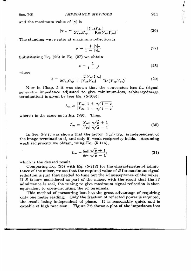
SEC. 7.3]
IMPEDANCE ME1’IIODS 211
and the maximum value of 1~1is
1~1~= 2G..GB: ?13il’=pYR.)”
(26)
The standing-wave ra tio a t maximum reflect ion is
1 + 17]m
p = 1 – l~lm”
(27)
Subst itu t ing Eq. (26) in Eq. (27) we ob ain
Now in Chap. 5 it was shown tha t the conver sion loss L~ (signa l
gener ator impedance adjusted t o give minimum-loss, a rbit ra ry-image
t ermin at ion ) is given by [see Eq. (5.109)]
where e is the same as in Eq. (29). Thus,
Lm=l
dl + +
1.
Iy#al <; -1
(30)
In Sec. 5.8 it was shown tha t the factor IY=61/[Y~al is independent of
th e image termina tion if, and only if, wea k r ecipr ocity holds. ssuming
ea k r ecipr ocit y we obta in , u sin g Eq. (5.116),
(31)
wh ich is th e desir ed resu lt .
Compar ing Eq. (25) with Eq. (5.112) for th e chara cter ist ic i-f admit-
t ance of the mixer , we see tha t the requ ir ed value of B for m aximum sign al
r eflect ion is just tha t needed to tune out the i-f susceptance of the mixer .
If B s now considered as pa r t of the mixer , with the resu lt tha t the i-f
admit tance is rea l, the tuning to give maximum signal reflect ion is then
equ iva len t t o open -cir cu it in g t he i-f t ermin als.
his method of measur ing loss has the grea t advan tage of requ ir ing
or dy on e met er readin g. On ly th e fr act ion of r eflected power is required,
the resu lt being independen t of phase. It is reasonably quick and is
I
capable of high precision . F igure 7.6 shows a plot of the impedance loss
212 LOS S AND NOIS E MEAS UREMENTS
~L=4P+l
<p-l
as a funct ion of the reading of Meter 2.
the ra t io of the meter reading with a crysta l reflect ing
[SEC. 73
Th e abscissa is
the signal t o the
r ea din g wh en complet e r eflect ~on i pr odu ced (by closin g t he r -f sh ut ter ).
This ra t io is equal to the fract ion of r eflected power [see Eq. (19)].
It should be noted that L~ depends on image terminat ion . The
image termina ion that applies to this measuremen t is of cou r se the par -
t icular one in the exper imenta l
12 -
appara tus. With the ar rangement
illust ra ted in F ig. 7.4, the image is
10 -
matched, tha t is, it is not reflected
back to the crysta l. The loss L~ can
8 -
be studied as a funct ion of image
n
u
impedance, by using a filter cir cuit
=6
in Arm 3 (see Fig. 7.5a). This filter
%
CJ
always t ransmits t he signal with out
4 -
r eflect ion bu t m ay r eflect t he im age.
The phase of the image reflect ion
2 -
can then b var ied by inser t ing a line
st r et cher between the filt er and the
o
) , 1
0
0,2
0.4
0.6 0.8
mixer . As an example, a bandpass
1.0
&
filter such as a TR tube may be in-
Po
FIO.7.6.—Conver s ion loss a s a funct ion
ser ted in Arm 3. BY this t echni ue,
of the fr act ion of reflect ed power .
Pound found tha t the largest and
smallest values of L~ as a funct ion of
the elect r ica l istance between this cavity and the mixe differed by
about 1.5 ,to 2.0 db for a number of crysta ls t ested.
Before leaving the subject of loss determina t ion by impedance
measurements it wou ld be well to discuss how far result s of th is t ype of
measur ement agr ee with cor respondin g result s obta in ed using m or e con -
ven t ional methods. Provided car e is t aken to com~are losses of the same
defin it ion , t her e is excellen t a gr eemen t in t he cas~ of all silicon cr ysta ls
and of some germanium crysta ls, but for other germanium crysta ls la i-ge
discrepancies are found. F ifty silicon and germanium crysta ls were
measured for Lo using both th Dicke impedance method and the Rober t s
amplit ude-modu la tion met hod.
In no case was a discrepancy larger
than 0.2 db found for the silicon units, but some of the germanium units
indica ted impedance losses as much as 3 db ess than the corresponding
direct ly measured values. It is reasonable to at t r ibute this discrepancy
to the reciprocity factor ga8/g~= since other measurements have shown
this factor often to be gr ea ter than unity in the case of germanium. In
no case was the impedance loss found to be gr ea ter than the direct ly
measu r ed loss.

SEC. 7.4]
AMPLIT UDE-MOD ULA T ION METHODS
7.4. Th e Incrementa l and knplitude-modula t ion
213
Methods. T lw
D-c Iwem zntal Method.—We now come to the methods of loss measure-
men t found to be most sa t isfactory in product ion test ing. As expla ined
in Sec. 7.1, the quant ity measured is
O.
By Eq.
(5.79), LO is given by
Zg
LO =
av
()
Pg”
(32)
P
th e a bsorbed local-oscilla tor power .
These quantit ies a re all easily
measurable. The part ia l der iva t ives a re not easy to measure direct ly
sin ce it is dli%cult t o mainta in on e var iable (V or P) cons ant while the
-EiEHE1
IG. 7.7a .—Block d iagr am of appa r at u s u sed in t h e in cr emen t al met hod of loss mea su r e
ment .
FIG.7.7b.—D-c cir cu it u sed in the incrementa l me thod of los s measu rement .
oth er is va r ied. The equat ion for LO can be so t ra nsformed, h owever , a s
to make measurement of the part ial der iva t ives unnecessary in order to
obta in a fa ir approximat ion to Lo.
A schemat ic diagram of the circuit used in the measurement of L,
is shown in Fig. 7.7. The crysta l is loaded by th resistance r l + rz,
wh ich is usually adjusted to about 400 ohms. The curren t supplied by
the ba t tery balances ou t the crysta l cu r ren t a t some standard r-f power
level P and makes the curren t in the microammeter zero. The I esistanc
TI d evelop s a d -c bia s volt a ge V a cr oss t he r ect ifier a t t he r -f power level P.
The r -f power is then increased by dP, pr odu cing a ch ange in r ect ified
curren t which is indica ted by the meter .
Th e cha ng in bias volt age dV
is t hen the product of the resistance,
1
== r l + T2,
G
(33)
by the change in cur rent , or
dV= –~dI.
(34)
——
—
214
f.OSS
A,VI) ,VOIS E MJ 9AS [J R MEN TS
[SEC. 74
xow any change in direct curren t dl is given by
dI=$; dV+$dP.
Eliminating dV a nd solvin g for aI/ aI’ gives
Subst itu t ing this in Eq. (32) we obta in
(35)
(36)
(37)
1n Ilq. (37) we may take PO t o be the average power , P ~dP. N ow
dI/ a V, by Eq. (5 .84 b), is the i-f conductance f the conver ter under
the condit ions of measurement . If gb is equal to t ll/t l V, t h e act or
4gb :V
(9’+W
is un ity and the loss is gi en by
(38)
(39)
This method is ordinar ily used in fixed-tuned measurements and gL,
is chosen to be equal to the mean i-f conductance of the type of crysta l
to be measured. For any one cry ta l the Factor (38) is genera lly less
than unity but the er ror involved in using Eq. (39) instead of Eq. (37) is
less than ~ db if
For rout ine measuremen s the F ctor (38) is usually dropped, ut it
nust be included in accura te work.
The loss is obta ined from Eq. (39) by measurement of gb, p,, dp, and
LI The change in curren t dI is dir ect ly in dica ted on t he m icr oammet er
md gb is accura tely measured with a br idge. The r-f power PO is meas-
u red with a bolometer and is a proper ty of the appara tus on ly.
It can
bc mainta ined constant by reference to standard crysta ls. The change
in power dP s produced by a change in a t tenuat ion between the crysta l
t
),
,’
I
I
I
18
1,
Ii
(

1
SEC.
7.4]
AMPLITUDE-MODULATION METHOD
215
I
and t he r -f oscilla tor . The a t t enua tor must be ca refu lly ca libra t ed fcr
I
t h is purpos e.
The d-c incrementa l method out lined here is not well adapted to
i
ra pid pr odu ct ion test in g.
It is used ra ther to establish an absolu te
ca libr a tion of st an da rd cr yst als
Th ese cr yst als a re t hen u sed t o ca libr at e
t he a ctua l pr odu ct ion t est appara tus, wh ich is of t h amplitu de-modula-
t ion t ype.
T he Am plitud e-nwdu .?u tion Method .—In t he amplitude-modu la t ion
method an r -f oscilla tor is ma tched to the mixer a t loca l-oscilla tor level
(= 1 mw). The ou tput of the oscilla tor is then modu la ted in amplitude
a t some low audio fr equency f?. The modu la t ion envelope is det ect ed by
the crysta l wh ich develo~s a volt age a t the fr equency P acros an ou tpu t
I
load. The conver sion loss LO may then be found from this voltage if the
,
percen tage modula t ion and the power of the oscilla tor a re kno n . This
method was develo ed independen t y by Smith l and Rober t s. 2
Th e
pa r t icu la r form now in genera l use is tha t of Rober t s and is the one
descr ibed h er e.
The amp itude-modula t ion method is simila r t o the d-c incrementa l
method in tha t n signa l power is used, it s funct ion being exercised by a
var ia t ion in power of the loca l oscilla tor . It is well known , however ,
t ha t a sinusoida l amplitu de-modu la t ed wa ve is equ iva len t t o a sinusoida l
ca rr ier plus t wo sinusoida l symmetr ica lly loca ted sidebands. Th e ca rr ier
in our presen t case can be conceived as the loca l-oscilla tor wave, and the
two sidebands as two signa ls, each sepa ra ted in frequency from the loca l
oscilla tor by the modu la t ion fr equency P, wh ich plays the role of in ter -
media te fr equency. Each signal sideband is the image of the other .
The problem of deducing the rela t ion between LO a nd obs er va ble
quant it ies in th is measurement can be s mply handled. Bu t to ake the
resu lt unambiguous, especia lly with r efer en ce t o th e pr ecise defin it ion
of the modula t ion coefficien t and to quest ions of coher ence of the bea t
product s from the two sidebands, we must go back to the fundamenta l
[
m ixer equ at ion s [Eq. (5.61)], r epr odu ced h er e.
H er e t he su bscr ipt s a , ~, a nd 7 den ot e, r espect i ely, t he sign al fr equ en cy,
in termedia t e frequency, and image frequent y; ia , et c. a r e the complex
ur ren t amplitudes; e., et c. t he complex volt age amplitudes a t he
~
termina ls of t he mixer ; ga a, e tc. a re t he elemen ts of t he a dmit t ance matr ix
I
1R. N . Smit h, ‘( Mea su rem en t of Con ver sion Ga in wit h a Modu la ted Oscilla tor ,”
,
NDRC 14-144, P ur du e Un iv., Apr . 20, 1943.
: S. Rober ts, RL Repor ts No, 53-23, J u ly 3, 1943, a nd No. 53-28, Au g. 3, 1943,

216
[SEC.74
of the mixer . In ou r present case both signa l and image waves are
incident on the crysta l and
giving
a>d
there is per fect symmetry between them,
~e =
The fact tha t t he signa l cu r ren t
Imaginarysis
Signal
I
I
FIG, 7.8.—Vect or r epr esent at ion of a n
amplitude-modulated wave.
i;
}
(41)
e?.
and volt a ge a re com plex con ju ga tes
of the cor r esponding image quant i-
t ies may be seen at once if we con-
sider the vector r epresen ta t ion of an
amplitude-modula ted wave.
Th e
volt age (or c r ren t ) of the car r ier
is a constant (rea l) vector and the
two sidebands are vector s of equa l
magnitude rota t ing with respect to
the car r ier in opposite direct ions.
The fr equency of the rota t ion equa ls
the modula t ion fr equency @ (see
F ig. 7.8).
The choice of t ime zero requir ed
to make the car r ier volt age rea l a lso
gives a rea l admit tance matr ix.
provided weak reciprocity holds. Thus Eq. (40) r educes to
i= =
(9.= + g=,)e. + 9a~e6
ifl = 2g~=e. + g~flefl
}
(42)
The “in termedia te fr equency
“ is now the modula t ion fr equency O,
and since the output of the mixer is loaded by a con-
ductance gb, we have
i~ =
‘gbefl.
K
(43) A
g
Th e oscilla tor is r epr esen ted by Nor ton ’s t heor em
as a constan t cu r ren t genera tor with an interna l con -
FIG.79.-Oscil-
ductance g as illust ra ted in Fig. 7.9.
later repr esentedas
The impedance offered by t he mixer t o t he ca rr ier ~c~~r ~&’t (Ac~r~~~
must be dist inguished from tha t offer ed to its side
in ter na l condu c -
bands. Under the condit ions of measurement the ““C’ ‘~)”
ca rr ier (wh ich r epla ces t he loca l oscilla tor ) is m at ch ed t o t he m ixer .
Th e
in terna l conductance g of the oscilla tor is thus given by Eq. (5.26);
g = g.. – g.,.
(44)
The conduct ance offered by the crysta l t o the sidebands will not , how-
ever , be g because of the fact tha t t he sidebands a re a t a low level with
SEC. 7.4]
AMPLITUDE-MODULATION METHODS
r espect t o the ca r r ier . The sidebands will not , t herefore,
t he m ixer .
(!
.:
217
F
be matched t o
\
If Am is t he magnitude of the cu r ren t genera t ed a t the sideband
frequ ency a , and
AO is
t he cor respon din g quan tity for ea rner , we h ave th e
u su al expr ession for amplit ude modu la tion
(45)
wh er e m, defin ed by th is expression , is t he so-ca lled “modula t ion coeffi-
cien t” of the oscilla t r . The cur ren t A. is equal t o the cur ren t i= in the
ixer plus the cur ren t gemin the conductance g, or
A= = i. + ge=. (46)
Eliminating A., iti, ea, ga,, and ie from Eqs. (42) to (46), inclusive, we
obtain
1
mAo = —eB
(
)
gbgm + gmg.tlfl — g.Bg8. .
z
9h
(47)
The i-f load conductance gb is normally chosen to equal he mean
i-f conductance, gp, of a la rge group of the type of crysta l to be measured.
For any par t icu la r cryst a l, however , gb will differ in genera l from gB.
Let us put
gb = ngb,
(48)
where by Eq. (5.84a)
9..9PP – 9a d9Ba
gb =
9..
(49)
is the i-f conductance of the mixer when the mixer is ma tched to the loca l
oscilla tor as in t he pr esen t ca se.
Su bst it ut in g Eqs. (48) and (49) in Eq. (47) we obta in
m21A012_
[ 1
4g=a(gaagp@– g=~g~=) .
— _
4
4n
99;.
(50)
Compar ing Eq. (50) with Eq. (577) we see hat the expression in the
square bracket s on the r ight of Eq. (50) is just LO.
Solving for thk we get
4n
mzp
‘0 = (1 + n)z g&j’
(51)
where we have put
P = IA 012/ 8g as the
available power fr om t he ca rr ier
and
EP = led]/ fi as
the rms modula t ion volt age across the load gb.
It must be noted tha t m is the modu la t ion coefficien t r efer r ed t o the
available power of the oscilla tor and not to the power actua lly sent in to
the crysta l a t t he sideband frequencies. 1
1See L. C. P et er son a nd F . B. Llewellyn , Proc. I . R .E . ,
I
..--– -

..--– -
218
{.
LOSS AND NOISE MEASUREMENTS [SEC.75
.
he expression 4n/(1 + n)’ appear ing on the r ight side of Eq. (51)
is ident ica l to the Fac or (3S) appear i g in the expression for
LO
in the
incr ementa l method. It is r eplaced by unity in product ion test ing.
The amplitude-modula t ion method may be used either as an absolu te
or as a r ela t ive method.
As a rela t ive method standa rd cryst ls (standardized by the incre-
menta l method) ar e used to establish the basis of measurement . Since
mj, P and gb are constan ts of t he appara tus they need not be measured
dir ect ly. The power P is adjusted to give the cor rect rect ified cu rren t
of the standard crysta ls. The modula t ion in product ion test ing is
usua lly provided by applying a 60-cycle volt age to the gr id of the oscil-
la tor . This voltage is then so adjusted tha t the cor rect readings for the
standard crysta ls a re obta ined on the outpu t a-c voltmeter .
The dial
of th is voltmeter is usua lly ca libra ted in decibels so tha t the loss
LO
can
be dire t ly read from this meter .
If the amplitude-modula t ion method is used as an absolu te method
on e must m ea su re
gbj P,
and mz: It is easy to measure gb with a br idge;
P
is determined with an r -f b lometer emp oying a thermally sensit ive
clement such as a 1$’ollaston wire or a thermistor bead. The modula t ion
coefficien t m is difficu lt t o measure if the modula t ion is applied elec-
t ronica lly. The modula t ion may be applied mechanica lly by the device
in Fig. 9.18 by which the coefficien t m may be measured with grea t
precision . A cardboard disk,’ one side of which is covered with a
resist ive coat ing of carbon , is mount ed eccent r ica lly on a motor -dr iven
axle (see F ig. 7.9).
The disk is ar ranged to penet ra te somewhat in to the
),a vegu ide or t ra nsmission lin e bet ween t he oscilla tor a nd cr yst al h older .
Eecause of the eccen t r ic mount ing the amount of penet ra t ion var ies
over one revolu t ion of the axle.
Since the power t ransmit ted is a t tenu-
a ted by an amount depending on the degree of inser t ion of the disk, the
t ransmit ted wave is modula ted in amplitude as the disk is turned by the
motor . The modula t ion may be made sinusoida l by proper mount ing
and shaping of the disk. The envelope of the t ransmit ted wave can be
accura tely determined by measur ing the t ransmit ted power in to a linear
matched load as a funct ion of angular posit ion of the disk. T e modula-
t ion coefficien t is then found from the envelope. Deta ils of th is method
a re given in Chap. 9.
NOISE -TEMPERATURE MEASUREMENTS
7.5. Genera l Considera t ions.—The measurement of noise t empera -
tu r e ca lls, like loss measurement , for two dist inct types of measur ing
equipment , namely, easily manipu la ted equipment adapted to accura te
and rapid rou t ine measurement as in product ion test ing, and equipment
1 Th e ma ter ia l of t he disk is t he same as t ha t u sed in ma kin g ca rbon r heosta ts.

SEC.
7.5]
GENERAL CONS IDERATIONS 219
for t he r esear ch labora t ory capable of measur ing th e n oise temper at ur e of
cr yst als wit h possibly widely va ryin g pr oper ties.
By defin it ion , th e noise t empera tu re is th e ra tio of th e available noise
power of the crysta l to tha t of a resistor a t a standard t empera ture,
chosen , for conven ience, to be 290”K [see Eq. (2.26)]. The available
noise power fr om a resist or at this temper at ur e in a bandwidth of 1 Me/see
is 4.0 X 10⁻¹⁶ wat t , and consequent ly a high-ga in amplifier is r equired
for the measurement . The ou tput power of the amplifier is measured
wit h a wa ttmet er .
With t he amplifier -meter combina t ion t he -fact or can be measured.
In Chap. 2 the Y-factor was defined as the ra t io of the ava ilable output
noise power IV. of an amplifier loaded by a crysta l mixer to the available
ou tput noise power N08when loaded by a standard resistor . In Eq. (232)
there was der ived for the noise tempera ture, in t erms of the Y-factor , t he
expression
t = F;.,(Y – 1) + 1.
(52)
The applica t ion of this equat ion is limited by the fact tha t both the
Y-factor and the i-f noise figu re are funct ions of the i-f impedance of the
crysta l; th e input impedance of th e amplifier changes w en th e standard
resistor is replaced by a crysta l of differen t impedance. Rober t s”
ana lysis, presen ted in th is sect ion , yields an expression for the noise
t emper atu re of a crysta l in terms of th e Y-fa ctor and of t he i-f admit tance
of the crysta l if a nar rowband amplifier is used. This method is not
a da pt ed t o r ou tin e t est in g, h owever , sin ce it r equ ir es a sepa ra te mea su re-
ment of the i-f impedance. Rober t sz has there ore designed a nondissi-
pa t ive circu i for coupling the crysta l and the amplifier which makes Y
independent of the crysta l conductance to a fir st approximat ion for the
r an ge of i-f con du ct an ce or din ar ily en cou nt er ed in commer cia l cr ysta ls.
Such a cir cu it for use with a nar rowband amplifier is discussed in Sec. 7.6,
and test set s incorpora t ing it a re descr ibed in Cha . 9.
The noise tempera ture can also be measured by an applica t ion of
Eq. (2.28). In this equat ion t he over -a ll noise figur e of a crysta l-mixer–
amplifier combin at ion is given by
F:- = L(t + F’. - 1),
(.53)
where L is
t he conversion loss of t he cr ys t ,a l,tis its n oise t emper at ur e, a nd
l’;., is t he efff,ct ive n oise figu re of t he:., amplifier . To ca lcu la te
trequires
measur ing F~~,
F{.,, L , and the { f resistance (which enter s implicit ly);
hence, thk, procedure is not adapted to rou t ine test ing. In developmen t
1S. Rober t s, “Theory of Noise Measurements on Qvsta ls as F requency Con-
ver ter s,” RL Repor t No. 6 i -11, J a n. 30, 1943.
: ~~. &
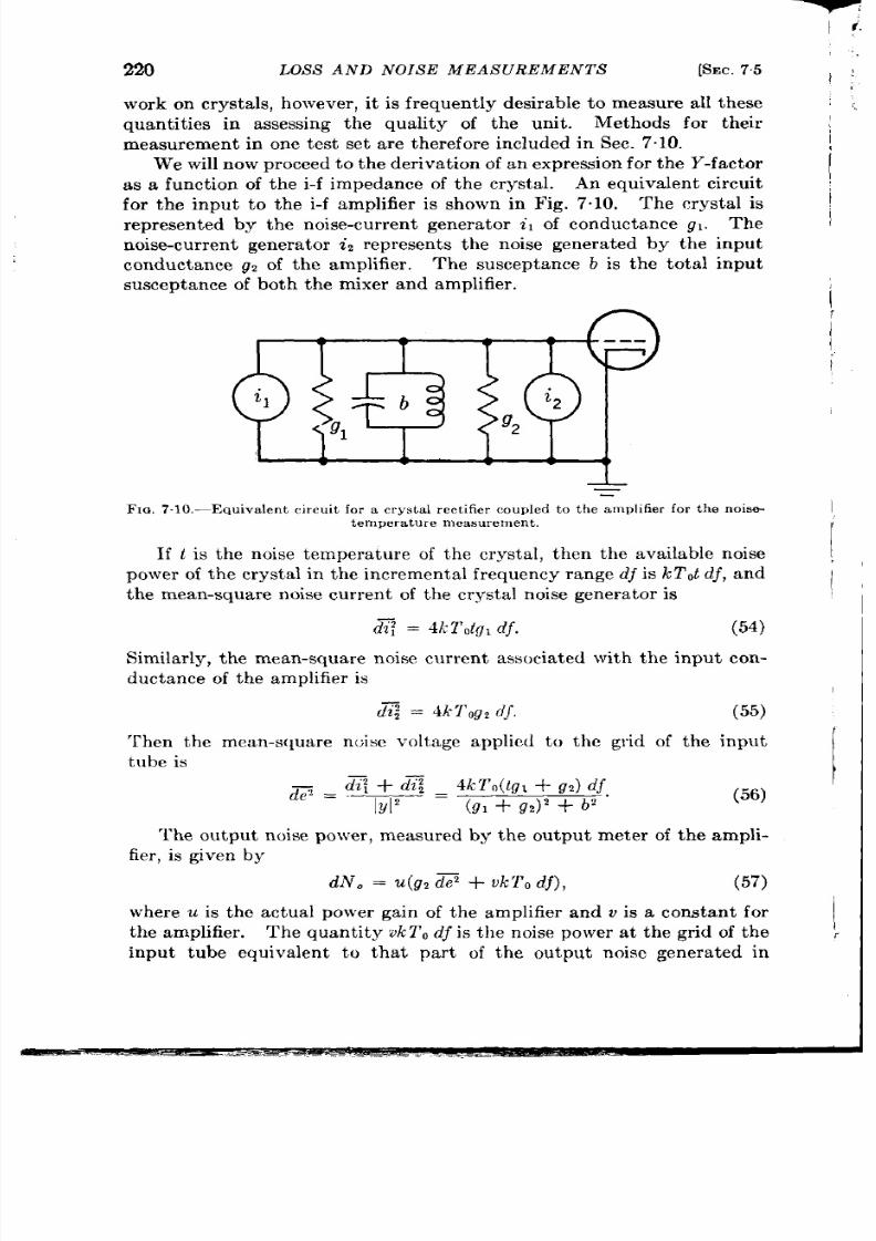
220
LOSS AND NOIS E MEASUREMENTS
[SEC.
75
wor k on crysta ls, h owever , it is frequen tly desirable t o measure all t hese
quant it ies in assessing the quality of the unit . Methods for their
measurement in one test set a re therefore included in Sec. 7.10.
We will n ow pr oceed t o t he der iva tion of a n expr ession for t he Y-fa ct or
An equ i a len t cir cu it
for the input to the i-f amplifier is sho n in Fig. 7.10. The crysta l is
r epresented by the noise-cu r ren t genera tor il of conductance g 1.
Th e
noise-cu r ren t genera tor i2 represent s the noise genera t ed by the input
con du ct an ce g2 of t he amplifier .
The susceptance b is the tota l input
susceptan ce of both t he mixer and amplifier .
—
=
F IG, 710.-Equ iva len t cir cu it for a cr ys ta l r ect ifier couple d t o t h e amplifier for t h e nois e-
tempera ture measurement .
If Lis the noise tempera ture of the crysta l, then the ava ilable noise
power of t he crysta l in th e incrementa l fr equency r an ge
df is k!l’, t dj,
and
the mean-square noise cur ren t of the crysta l noise genera tor is
Similar ly, t he mean-square noise cu rr en t associa ted with th e input con -
du cta nce of t he amplifier is
d~ = 4kT ,g, d~.
(55)
Then the mean-squar e n ,;ise voltage applied to the gr id of the input
tube is
d7 .
d~:+ d~
4kTo(tg, + g,) d f,
IY12 =
‘(Q, + o)’ + b’
(56)
Th e outpu t noise power , measured by the outpu t meter of the ampli-
fier , is given by
dNo = u(g, d~ + vkTo dj), (57)
where u is the actual power ga in of the amplifier and v is a constan t for
the amplifier . The quant ity ok T , d f is the noise power a t the gr id of the
input tube equiva len t to tha t par of t he outpu t noise gener a ted in
I
r
f
!

SEC. 75]
GEN ERAL CON SIDER ATION S
221
the amplifier it self. The fir st term of Eq. (57) is the con t r ibut ion to the
output power from the actua l power input to the am lifier , ga d~z.
Combining Eq. (56) and (57), w obta in
I
[
1
4g’(tgl + ‘2) + V df,
‘N o = ‘kTO (gl + g,)’ + b2
and
H
.
No = kT ,
492(t91 + 92)
o
1
(g, + g,)’ + v + v ‘f”
(58)
(59)
I
For an amplifier whose bandwidth is small compared wi h tha t of the
1
input circu it it can be assumed tha t
b, gl, g~,
and
t
a re const an t over the
I
range of in tegra t ion , hence Eq. (59) may be writ ten ,
[
492(t91 + 92)
/
/
0 = ‘T” (91 + 92)2 + b’ ‘dj + ‘To ‘v ‘j’
(60)
where the in tegra t ion is to be car r ied ou t over the pass band of the
na r rowband amplifier .
To obta in the Y-factor an expression is r equ ir ed for the noise-power
ou tput N.. when the crysta l is replaced y a standard resistor of con-
1
ductance g,. The susceptance
b is
t uned ou t for th is measurement .
i
Hence, s et t ing b = O, t = 1 and replacing gl by g. in E . (60), we obta in
4g,
No, = kT , —
[
U dj + kTO
UV dj.
g. + g2
Also fro Eqs. (2.12) and (2.13) we ha e
,.
(61)
(62)
where
F;
a nd G. a re, r espect ively, t he effect ive n oise figu re a nd ga in of t he
i-f amplifier with a signa l enera tor of the same conductance as the
I
standard resistor . The quant ity G, is the ra t io of the power delivered
t o th e out put et er t o t he available input power fr om t he signal gen er at or .
We now need an expression for G, in terms of U, g., an g’. The ou t -
put -meter reading & is propor t iona l to the input power ,
S o = ug2e~.
(63)
With an i-f signa l genera tor of conductance g. and shor t -circu it cu rent
il, t he available power from the signa l genera tor is
s, = *,. (64)

222
lt ’ith t his signal
volt age is
J .OSS A ,VJ~ ,VOIS E ,J IEA S UliEMI$N 7’,S
[SEC. 75
gener to connectu l to the input termina ls the inpu t
~1 . J1_.
(65)
Q. + gz
Combin in g Eqs. (63), (64), and (65) >VCobtain
A!so
4g,g2
‘“ =R = ‘(% + 92)’”
(66)
Th e subst itu t ion of Eq. (66) in Kq. (62) gives
No, =
IWCTO$ : ~ ~
[
u dj.
(67)
8
Combining Eqs. (60), (61), and (67) we obta in
{
1-=:=: @’+g’)(g’+g’J’-:–
If; ga[(g, + g,)’ + b’]
I
+1.
(68)
OS
f the susccptance b is tuned out for each measurement , t can be calcu-
2,4
2.2
–
2,0
1,8
–
z
~ 1.6
A
1.2
–
1.0
–
0.8
I
0.5 1.0
2.0
Crystal conductance in units of standard
conductancePCgl / gg
FIG. 71 1.—Y-factor as a fun ct ion of
cr ys ta l conduct a n ce,
with the crysta l
coupled direct ly to the amplifier , for var ious
va lu es of t .
Ia t ed from measurement s of Y and
J 1. If t he r -f termina ls of t he mixer
a re t ermina ted with the same
impedance at signal and image
frequencies, t he var ia t ion in crys-
ta l suscept ance from crysta l t o
crysta l is small and can be tuned
out approximately with a fixed
adjustment.
To invest iga te the eff ect of var i-
a t ion in cryst al onduct ance on the
Y-factor , let us wr ite Eq. (68) in
simplified form by put t ing gl = pg.
and gz = mg,. Assumi g
b = O,
we obtain
[
1 tp + m )(l + m )z
Y=p
.
(p + m )’
1
—
1
—l +1.
(69)
If the crysta l conductance is equal
to the standard conductance, then
P = 1 and Eq. (69)
reduces to Eq.
(52).
F igu re 7.11 presen t s Eq. (69) gr ph ica lly for differen t va lues of t ;
Y is plot ted as a funct ion of p for va lu es of p from 0.5 to 2. Values of
II
II
1’

.
,
SEC. 76]
THE ROBERTS COUPLING CIRCUIT
223
F; = 4 (6 db) and m = 1 were used in plot t ing the graph. An inspect ion
of Fig. 7.11 gives an idea of the er rors t be encoun tered if th e dependence
of Y-factor on crysta l conductance is ignored. For example, a crystal
with a noise tempera ture of and a conductance of 0.5g, has a larger
Y-factor than a crysta l with a noise tempera tu re of 3 and a conductan ce of
2g.. The range from 0.5g, to 2g8 plot ted in Fig. 7.11 is sufficien t to cover
t he dist ribu tion of i-f r esist an ce in commer cia l r ect ifier s.
7.6. Th e Rober ts Cou plin g Cir cu it .-A n on dissipa tive cou plin g cir cu it
designed by Rober tsl makes the Y-factor independent of crysta l imped-
ance to a first approximati n, provided that (1) variat ions in crysta l
susceptance are small enough to permit the susceptance to be tuned ou t
with a fixed adjustment , and (2) the band-
D-* ::,er
width of the i-f amplifier is sufficien t ly
The coupling network also serves
a usefu l funct ion as an impedance t rans-
former which matches the crysta l to the
Crvstal
Ampllfier
. .
F IG. 712.-Block dia gr am of
The coupling network is shown in block
inpu t coup ling ne twork for nois e-
diagram in Fig. 7.12. The crysta l conduct -
tempera ture measurements .
an te g; is connect ed to the inpu t termina ls
of the coupling network; the input terminals of the amplifier , having a
conductance gz, are connected to the output terminals of the network.
The admit tance presented by the output terminals of the network is
gl + jb, in a ccor da nce wit h t he n ota tion of t he pr ecedin g sect ion .
Consider ing gl and b as the only variables in Eq. (68), we may wri e
(70)
If Y is to have a sta t ionary value for g{ = g,, then it is necessary that
( )
Y
—t
dgl 0’,-0.
= o. (71)
We see from Eq. (68) tha t d Y / db = O when b = O. If, also,
( )
g,
@ O’l=g.
= o,
it is evident from Eq. (70) that the condit ion of Eq. (71) is sa t isfied.
The two condit ions tha t the network must sat isfy, therefore, a re (1)
b=o when g{ = ga,
1S. Roberts,
“ Theory of Noise Measu rements on Crystals w Frequency Con-
ver ters,” RL Repor t No. 61-11, J an . 30, 1943.

224
LOSS AND NOIS E MEASUREMENTS
[Sm . 76
and (2)
( )
dg, ~ , ,. ,
o.
Both these condit ions can be obta ined
-tiu,
m
with a simple II-network, such as tha t
shown in Fig. 7“13; the network also
ser ves as a n im peda nce t ra nsformer for
matching the crysta l to the amplifier .
Let us express the admit tances of the
elements of the network in units of o, as
FIG. 713.-Input coupling network
. .
for a na r rowband amplifier ,
shown in Fig. 7.13, and let n be the im-
pedance stepup ra t io of the network.
Then
~l=$=g, P?42
p’ + (g – z)”
(72)
and
b=g,
[
Zy(y — z) — pzy
1
2+(Y– Z)2 +2”
From Eq. (73) we see tha t
b = O for g! = g. (or p = 1), when
The second condit ion of the preceding pa ragraph is sa t isfied when
( - )
g,
d ,=1
= o,
(73)
(74)
or
(y – z)’ = 1. (75)
Combining Eqs. (75) and (72) and set t ing p = 1, we obta in
(76)
Then,
Z=y+l,
Z=yk+yz.
}
(77)
Subst itu t ing Eqs. (76) and (77) in to Eqs. (72) and (73), we obtain
(78)
I
}
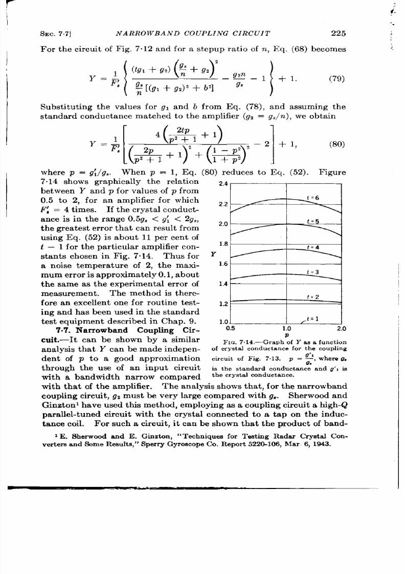
i.
SEC. 77]
NARROWBAND COUPLING CIRCUIT
225
For the circuit of Fig. 7.12 and for a stepup ra t io of n , Eq. (68) becomes
I
( )
2
(tgl + 92) : + 92
Y=;,
gt n
.——
1
1 +1.
(79)
8
: [(91 + 92)2 + ~zl “
Subst itu t ing the va lues for g, and b from Eq. (78), and assuming the
standard conductance matched to the amplifier (gz = g./n ), we obta in
[
4 ( %+ ’ )
1
=+
P%+)+(W”21’ ’80)
where p = g~/g,. When 1, Eq (80) reduces to Eq. (52). F igure
7.14 shows graph ica lly th rela t ion
between Y and p for va lues of p from
0.5 to 2, for an amplifier for which
F: = 4 t imes. If the crysta l conduct -
ance is in the range 0.5g. < g; < 2g,,
the grea test er r or tha t can resu lt from
using Eq. (52) is about 11 per cen t of
.! – 1 for the par t icu lar amplifier con-
stants chosen in Fig. 7“14. Thus for
a noise tempera tu re of 2, th e maxi-
m um er ror is a ppr oxim at ely 0.1, a bou t
the same as the exper imen ta l er ror of
measurement . The method is there-
for e an e cellen t one for rou t in e test -
ing and has been used in the standard
te t equ ipment descr ibed in Chap. 9.
7.7. Nar rowband Coupling Ci -
cu it .-It can be shown by a similar
analysis tha t Y can be made indepen-
den t of p to a good approximat ion
th rough the use of an input circu it
with a bandwidth nar row com~ared
‘ “ ’ ——l ———l
1.0
t .1
0.5
1.0
2.0
P
FIQ. 7 .14.—Graph of Y as a funct ion
of cr ys ta l conduct ance for t h e coup ling
circuit of Fig. 7.13. p = ~, where L?,
is t he st an da rd con du ct an ce a nd g’, is
the crys ta l conductance .
with tha t of the amplifier . Th~ analysis shows th t , for the na rrowband
coupling circu it , gz must be very la rge compared with g.. Sherwood and
Glnzton’ have used th is method, employing as a coupling circu it a h igh-Q
para llel-tuned circu it with the crysta l c nnected to a tap on the induc-
t n ce coil. For such a circu it , it can be shown tha t the product of band-
1E .
Sh er wood an d E. Ginztcm,
“Techniques for Te t ing Radar Crystal Con-
vertem and Sane Results ,” Spsr ryGyroscopeCo. Repor t 522V106,Mar 6 , 1943.
..
.——
226 LOS S AND NOIS E MEASUREMENTS [SEC.78
width and i-f crysta l resistance is constant ; the crysta l noise voltage
appli d to the gr id is th er efore independent of th e crysta l con du ctance,
provided the crysta l conductance is not so la rge tha t the bandwidth of
the input circuit exceeds tha t of the amplifier . Circuit s designed by
Sherwood and Ginzton were suitable for a range of i-f resistance from
about 250 to 2000 ohms. The method has not been used extensively for
cr yst al-test in g, h en ce fu rt her deta ils will n ot be given h er e.
7.8. Use of th e Noise Diode in Noise-tempera tu re Measurements.—
It was poin ted out in Chap. 6 that the mean-square noise curren t gener -
a ted in a tempera ture-limited diode is given by
~ = 2eI Af,
(81)
in the frequency band f to f + A~, where e is the elect ronic cha rge and I
is the diode curren t . If the diode is connected to a load resistance R, the
mea n-squ ar e n oise volt age a cr oss t he r esist or ar ising fr om t he diode n oise
is
~ = 2eIR2 Af.
(82)
The mean-square noise voltage arising from J ohnson nois is “
~ = 4kTOR Af;
(83)
h ence the tota l mean- quare noise volta ge across the resistor is
The available noise power from the resistor is
- ‘ k T OA ’ ( l%) ”
‘=4R
(84)
(85)
It is clear , then , tha t the effect of the diode current is to make the
resistor noisier by an amount tha t can be calcula ted from a measurement
of the diode curren t . The noise t empera tu re of the “noisy” resistor is
-+1=20ZR +1,
t = 2/cTO
(86)
when TO = 2 0°K, and 1 is the diode current expressed in amperes.
The noise diode thus provides a source of var iable, known noise
tempera ture or a means of adding known amounts of available n ise
power to the input circu it of an amplifie . Its use for absolu te measure-
men t is a pplica ble t o in termedia te fr equ en cies, wh er e R can be accu r at ely
determined. It has been used with some success, however , as an r-f
noise sou r ce for r ela t ive noise-figu r e measu r emen t s.
SEC. 79]
MEASU EMENT OF RECEIVER NOIS E FIGURE
227
An example of the applicat ion of the noise diode is the calibrat ion
of noise-tempera ture appara tus such as the standard sets descr ibed in
Chap. 9. In this applica t ion the standard resistor is in ser ted in the equip-
ment and the noise diode is connected. The ou tpu t meter can then be
calibra ted direct ly in terms of noise t empera tu re by means of Eq. (86).
A second applica t ion of the noise diode is the measuremen t of noise
figures of i-f amplifiers, accomplished as follows. With the noise diode
off and a resistor connected to the input terminals of the amplifier , the
output noise power is given [see Eq. (2.15)] by
N . = kT oF[.$li.~ Aj, (87)
where
F{.f
is the effect ive noise figu re and Gi.f is, as usual, the ra t io of the
power measured by the output meter to the available input power .
With the noise diode on , the available input -noise power from the
diode curren t is, from Eq (82),
P=&,
(88)
so tha t
* kTO Aj = 201RkT, Af.
p = 2kT0
(89)
The tota l amplifier ou tpu t power is then
N = k!f’dli-f Af (F{-, + 201R).
(90)
From Eqs. (88) and (90),
N
201R
~o=~+F(+’
(91)
whence
201R
F[~ = ~.
(92)
——
No 1
It is customary pract ice to adjust I so as to make N =
2No;
then
F{.f = 2011R ,
(93)
where II is the diode cur ren t required to double the noise output .
Diode noise genera tors are included in the standard test equipment
descr ibed in Chap. 9, and deta ils of const ruct ion will be given there.
MEASUREMENT OF LOSS, NOISE , AND RECEIVER NOISE F IGURE
7.9. The Measurement of Receiver Noise Figure.-It has been shown
in Eq. (2 15) tha t the effect ive noise figure of a network is given by
N.
“ = kT ,BG”
(94)
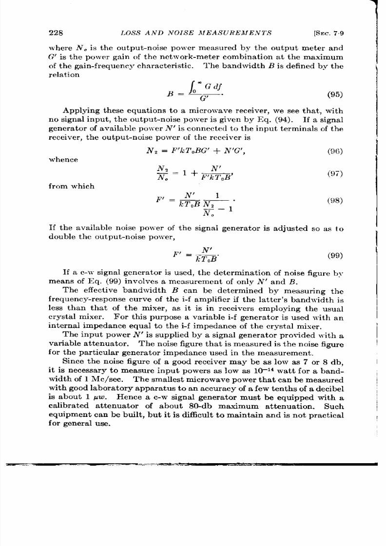
228
LOS S AND NOIS E hlEAS UR h’MEN l’S
[SEC. 79
where No is the output -noise power measured by the output meter and
G’ is the power ga in of the network-meter combinat ion at the maximum
of t he ga in -fr equ en cy cha ra ct er ist ic.
Th e ba ndwidt h
B
is
defined by t he
relation
B=~”GdJ
G’ “
(95)
Applying these equat ions to a microwave receiver , we see that , with
no signal input , the output -noise power is given by Eq. (94). If a signal
genera tor of available power N’ is connected to the input terminals of the
r eceiver , t he out put -noise power of t he r eceiver is
N , = F’kToBG’ + N’G’, (96)
whence
N,
N’
x = 1 + F’k T ,B’
fr om which
(!)7)
(98)
If the available noise power of the signal genera tor is adjusted so as to
double t he ou tpu t-n oise power ,
~, - N’
kT,B”
(99)
If a c-w signal genera tor is used, the determinat ion of noise figure by
means of Eq. (99) involves a measurement of only N’ and B.
Th e effect ive ba ndwidt h B can e determined by measur ing the
frequency-response curve of t he i-f amplifier if the la t t er ’s bandwidth is
less than that of the mixer, as it is in receivers employing the usual
crysta l mixer. For th is purpose a variable i-f genera tor is used with an
internal impedance equal to the i-f impedance of the crysta l mixer .
The input power N’ is supplied by a signal genera tor provided with a
var iable a t t enua tor .
The noise figure that is measured is t he noise figure
for t he par t icular gener at or impeda nce used in t he measurement .
Since the noise figure of a good receiver may be as low as 7 or 8 db,
it is necessa ry to measure input powers as low as 10–14 wat t for a band-
width of 1 Me/see. The smallest microwave power tha t can be measured
with good laboratory appara tus t o an accuracy of a few tenths of a decibel
is about 1 pw. Hence a c-w signal genera tor must be equipped with a
calibra ted a t t enua tor of about 80-db maximum at tenuat ion.
Such
equipment can be built , but it is difficult t o mainta in and is not pract ica l
for gen er al u se.
-
4
SEC. 7.9]
MEASUREMENT OF
A noise gen er at or employin g
devel ped for use in the I&cm
RECEIVER NOISE
t he 417A klyst ron
FIGURE
229
as a diode has been
band by Waltz and Kuper . 1 In th is
\
a pplica tion t he r eflect or is con nect ed t o t he ca vit y t o pr even t oscilla tion s,
and the tube is opera t ed a t a h igh voltage to insu re sa tura t ion and low
trans t t ime. The outpu t -noise power is propor t iona l t o the ca thode
cu rr en t, bu t Eq. (81) does n ot a pply beca use of t ra nsit it ime effect s.
Since
the !oad condu tance is not known with any cer ta in ty, ca libra t ion is
r equ ired for absolu te measurements. The range of available power is
sufficien t to measu re n ise figu res up to about 30 db, and the bandwidth
is approxima tely 2.5 Me/see. With a cavit y volt age of abou t 1500 volt s,
the ou tput power is constan t to abou t 1 db when the cavity is tuned over
>
the ra ge from 9 to 11.5 cm. This device is found to hold its ca libra t ion
*
over on g per iods of t ime and is su itable for gen era l field u se; a cor rect ion
must be made, however , when the bandwidth of the receiver being
measured is grea t er than tha t of the noise source.
In the 3-cm range simila r noise sources have been const ructed, using
the type 723A tube. Since the ou tput noise is a cr it ica l funct ion of
volt age and frequency, such use is r est r ict ed t o the labora tory, where
they may be ca libra ted in situ by a method such as tha t descr ibed in
Sec. 6.5. For a more deta iled accoun t of noise sources the reader is
I
r efer r ed to Vol. 11 of the Radia t ion Labora tory Ser ies.
i
Anoth r usefu l r -f noise genera tor is a cryst a l excit ed by d-c bias in
\
th e back dir ect ion , as discussed in ec. 6.5. The crysta l can be ca libra ted
for a given d-c bias by the methods descr ibed in tha t sect ion . This noise
source has the advantage tha t the output -noise power is independent
of the fr equent y and propor t iona l to the bandwidth ; the bandwidth
th erefore cancels ou t in the noise-figure measu remen t . If L is the r -f
I
noise t empera tu re of the crysta l for a given d-c bias, t hen the available
n oise power is
N’ =
kToBii+
(loo)
Equa tion (98) th en becomes
tr.f
“ = N, ~“
(101)
\
——
N.
The ra tio NZ/NO can be conven ien tly measu red with a squa re-law ou tpu t
meter connected to the termina ls of the receiver , such as a bolometer or
a crysta l oper at ed in t he square-law r egion .
For a more complet e discussio of noise-figure measurements the
reader is r efer r ed to Vols. 1S and 23 of the Ser ies.
;\
1M. C. Waltz and J . H. B. Kuper ,
“Simplified Mea su r emen t of Receiver Sen si-
t ivit ies, ” RL Repor t No, 443, Sept . 17, 1943.
230
LOSS AND NOISE MEASUREMENTS [SEC.7.10
7.10.
The Measurement of Mixer-crysta l P roper t ies.-It is often
desirable in the course of crysta l development to measu re the var ious
m ixer -cr yst al qu an tit ies u nder ver y gen er al con dit ion s.
A conven ien t
method is to use a crysta l as an r- noise source and a noise diode as an
i-f noise source with the appara tus shown in Fig. 6.11. With such
equip en t it is possible to measure the i-f resistance, loss, and noise
t empera tu re of the receiver crysta l, t he i-f noise figu re, and the over-a ll
r eceiver noise figure. The method is applicable to receiver s for which
the outpu t power is a funct ion of the i-f resistance at the input terminals.
The input circu it of such an i-f amplifier is shown in Fig. 7.15. The diode
Tomixer
Noisedmde T
I:IG. 7.15.—Input circuit for the
laboratory measurementof mixer crystal
properties.
noise source is connected th rough a
blocking condenser to the crysta l
mixer . It funct ions as a constant -
cu r ren t noise genera tor with the con-
duct ance of th e crysta l or the standard
resista nce ca rt r idge used for ca libra-
t ion , as the case may be. The single-
t un ed cir cu it of r esist an ce
Rl
can be
tuned to esonance with the variable
condenser C; th is is done with each
measurement , hence the input imped-
ance is a pu re resistance. The input conductance of the amplifier can be
adjusted with the resistance Rz.
F ilt er s, r epr esen ted by
LZ
and
L~,
serve
to decouple the power supply and the -c terminal of the mixer a t in ter -
med ia t e fr equency.
Measurem ent of Crystal I-f
Resistance.-For th is measuremen t the r -f
noise source is tu rned off.
Let
PI
and
PZ
be the available input noise
power with the i-f noise source tu rned off and on, and with a resistor
ca r tr idge of r esist an ce
R
in the mixer .
Then , from Eq. (85),
P, – P, = 201RlcT ,
Af.
(lo2)
The difference in outpu t noise power of th e amplifier with th e noise diode
on and off is
N, _ NI = AN =
201RkT~G,.,
Af =
F(R). (103)
The gain Gi.~is the ra t io of the power measured by the ou tpu t meter to the
available input power , and is therefore a funct ion of
R. Equat ion (8 )
a lso applies when the resistor is r eplaced by a crysta l, R
in t his ca se bein g
the i-f crysta l resistance. To determine the i-f resistance of the crysta l,
the u tput meter is ca libra ted by measur ing AN for a ser ies of resistor
ca rt ridges wit h va riou s va lu es of
R,
k eepin g 1 con st an t a t a pr edet ermin ed
value.
With the crysta l in ser ted, AN is read for the given va lue Of I,
and R det ermin ed fr om t he ca libr at ion cu rve.

SEC. 7.10] MEASUREMENT OF MIXERCRYSTAL PROPERTIES
231
Mea.surenwnt of Receiver N m”se
[email protected] receiver noise figure is
measured by means of the r -f noise source, as descr ibed in the previous
section.
Measu ren um t of Con version
Loss.—The con version loss of th e crysta l
is ca lcula ted from noise-diode measurements and the known values of
R
and
FL .
With the noise diode off and the crysta l in the mixer , the ou tput -
noise power is
N, = kT&t3k
Af = kT&i-GzFL. Af,
(104)
wh er e G= is th e conversion gain of th e crysta l.
With the noise diode on, the outpubnoise power is
N~ I Ns + 201R$c T~Gi.,
Af,
(105)
where R=
is t he i-f resistan ce of th e crystaL
Combining Eqs. (104) and (105), we obtain
whence
(106)
(107)
Measurenwnt of N oise T em perature.—Once
t he r eceiver n oise figu re,
con version loss, and noise figur e of th e i-f amplifier ar e kn own , t he n oise
tempera tu re can be calcula ted from th e rela t ion
F:m = LJF(., + t –
1).
(108)
Th e n oise figu re of t he i-f amplifier
F[~
depen ds on t he in pu t con du ct an ce;
it can be measured as a funct ion of
R
by means of the noise diode and the
standard resistor ca r t r idges. With a resistor ca r t r idge in place and the
noise diode off, t he noise ou tpu t of the amplifier is
N1 = k
T~G,_~F{-~
Af. (109)
Combining Eqs. (109) and (103) we obta in
201R
‘:-f = N2 ~“
——
N,
(111)
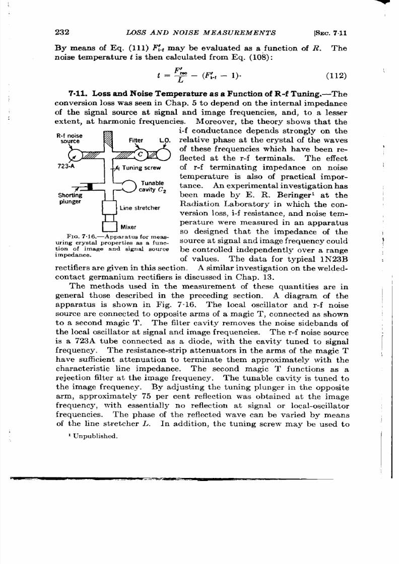
232
LOS S AND N OIS E MEAS UREMENTS
[SEC.7.11
By means of Eq. (111) F[.f may be eva lua t ed as a funct ion of R. Th e
noise tempera tu re t is then ca lcu la ted from Eq. (106):
t = > – (F:.f – 1). (112)
7.11. Loss and Nois Tempera tu re as a Fu nct ion of R-f Tun ing.-The
conver sion loss was seen in Chap. 5 t o depend on the in tern l impedance
of the signal sou rce a t signal and image frequencies, and, to a lesser
exten t , a t ha rmonic frequencies. Moreover , t he theory shows tha t the
R-f noise
source
Filter LO.
723-A
7?
Tunable
cavity C2
Shorting
plunger
Line stretcher
U Mixer
FIQ.7.16.—Apparatus for meaa-
u rin g cr yst al p roper ties a a a fu n c-
t ion of image and simm l sou rce
impedance. –
i f conductance depends st rongly on the
rela t ive phase a t the cryst a l of the waves
of these frequencies which have been re-
flect ed a t the r -f termina ls. The effect
of -f termina t ing impedance on noise
tempera ture is a lso of pract ica l impor-
ta nce. An exper iment a in vest iga ion has
been made by E. R. Ber inger l a t t he
Radia t ion Labora tory in which the con-
ver sion l ss, i-f r esist an ce, a nd n oise t em -
pera tu re wer e measu red in an appara tus
so designed tha t the impedance of the
sou rce a t sign al a nd im age fr equ en cy cou ld
be con t rolled independen t ly over a range
of va lues. The data for typica l 1N23B
rect ifier s a re given in th is sect ion . A similar invest iga tion in t he welded-
con tact germanium rect ifiers is discussed in Chap. 13.
The met ods used in the measuremen t of these quant it ies a re in
genera l those descr ibed in the preceding sect ion . A diagram of the
appara tus is shown in Fig. 7.16. The loca l oscilla tor and r-f noise
source a re connected to opposit e arms of a magic T, connected as shown
to a second magic T. The filt er cavity removes the noise idebands of
the loca l oscilla tor a t signa l and image frequencies. The r -f noise source
is a 723A tube connected s a diode, with the cavity tuned to signa l
fr equency. The resist ance-st r ip a t t enua tors in the arms of the magic T
have sufficien t a t tenuat ion to termina te them approxima tely with the
charact er ist ic line impedance. Th second magic T funct ions as a
r eject ion filt er a t t he ima ge fr equ en cy.
The tunable cav ty is tuned to
the image frequent y. By adjust ing the tuning plunger in the opposit e
arm, approximately 75 per cen t reflect ion was obta ined at the image
frequency, with essent ia lly no reflect ion a t signa l or loca l-oscilla tor
fr equencies. The phase of the reflect ed wave can be va r ied by means
of the line st r et cher
L. In addit ion , the tuning screw may be used to
1Unpublished.

SEC. 7.11]
DEPENDENCE OF R-F TUN ING
233
t une the signa l independen t ly. The amplifier inpu t circu it was tha t
shown in Fig. 7.15.
Result for a randornl y select ed sample of N23B crysta ls a re shown
in Table 7.1. These data wer e t aken with a signa l fr equent y of 9423
Me/see and an image frequency of 9363 Me/see. The tuning screw S
was not used; hence the impedance of the source a t signa l fr equency was
t he line impeda nce.
All measu rement s were t aken with 0.90 ma of
r ect ified cu rren t and n o d-c bias on th e crysta l.
The fir st and th ird row,
T.mnx 7.1.—EFFECTONCRYSTALROPERTIESFTHEPEASEOFREFLECTEDWAVE
AT IMAGEFr eqUenCy
For each crys t al, t he da ta in the fir s t and th ird rows a re for the phaseswhich give
maximum and minimum i-f resis tance,resr)ect ivelv:the second row is for a match at
bot h sign al a nd image fr equ en cies
Crys ta l No.
1
2
3
4
5
R
455
330
210
560
325
185
610
415
270
520
325
218
390
282
180
t
1.5
1.9
!.5
1.4
1.3
1.2
2.1
1.9
2.0
1.9
1.8
1.4
1.6
1,4
1,3
L, db
6.8
6,6
7.6
5.6
6.0
6.8
5.8
6.4
6.5
7.0
7.5
6,6
6.9
8,0
t/ R
0.0034
0.0058
0.0072
0.0025
0,0040
0.0034
0.0046
0.0074
0.0037
0.0055
0.0064
0.0041
0.0050
0.0072
.
for each cryst a l, give the data when the image phases a re such tha t the
i-f resistance is a maximum and minimum, respect ively; the second row
gives the resu lt s when there is a ma tch a t both image and s gnal fr e-
quencies. The var ia t ion in conve sion loss is abou t 1 db for va r ia t ions
in R of more than a factor of 2. The noise-t empera tu re var ia t ion , how-
ever , is less than 25 per cen t ; in some cases th ere is no sign ificant change.
If we con sider t he cr ysta l as a noise gen er at or f sh unt resista nce R, then,
k7’otf = ~.
(113)
from which ~’ = t/ R . It can readily be seen tha t with changes in image
phase the sil con crysta ls a re much more like a source of const an t noise
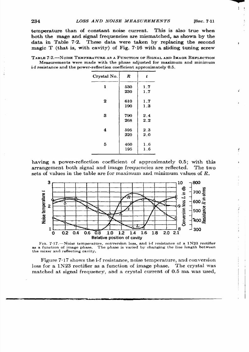
234
t empera ture
LOS S AND NOIS E MEASUREMENTS [SEC.7.11
than of constan t noise cu r ren t . This is a lso t rue when
both the mage and signal frequencies a re misma tched, aa shown by the
da ta in Table 7“2. These da ta were taken by replacing the second
magic T (tha t is, with cavity) of Fig. 7“16 with a sliding tun ing screw
TABLE7.2.—NoIsE TEMPEBATUaEAS A FUNCTIONOFSIGNALANDIMAGEREFLECTION
Measuremen t swere made with the phaae ad jus t ed for maximam and min imum
i-f rea iat an cean d th e power-reflectioncoefficient approxima tely0.5.
CrystalNo. R
1
530
230
2
610
190
3
790
268
4
I
595
220
5
460
195
t
1.7
1.7
1.7
1.3
2.4
2.2
2.3
2.0
1,6
1,6
having a power -r eflect ion coefficien t of approxima tely 0.5; with t is
a r rangemen t both signa l and image frequencies a re reflect ed. The two
sets of va lues in the table a re for maximum and minimum v lues of R.
v
) -h
-L
1’
E
% I
I I
A
%
1/
0.6 0.8 .1.0 1.2 1.4 1.6 1.8 2.0 2.~
Ii-
o 0.2 0.4
Rela t iveposit ionof cavit y
F IQ. 7 17.—Nois e t emper a tu r e, conver sion loss , a nd i-f r es is ta n ce of a 1N23 r ect ifier
as a fu nct ion of im age ph ase.
Th e ph ase is va ried by ch an gin g t he lin e len gt h between
the mixer and reflect ing cavity .
1,
I
J
F igu re 7.17 sh ows t he i-f r esist an ce, n oise t emper at ur e, a nd con ver sion
loss for a 1N23 rect ifier as a funct ion of image phase. The cryst a l was
m tched a t signa l fr equency, and a crysta l cu r r en t o 0.5 ma was used,

SEC. 711]
DEPENDENCE OF R-F TUNING
235
with self-bias from th e d-c met er r esist ance (abou t 100 ohms). Th e ph ase
was va r ied by means of the line st r etcher ; the abscissa is the rela t ive
posit ion of the cavity as the effect ive line length is changed. The dis-
t ance from cavity to crysta l increases as the abscissa increases, and the
range cover s approxima tely a complete cycle of image phase a t the
crystal.
I
I
I

CHAPTER 8
BURNOUT
8.1. Genera l Considera t ions.—Contrary to widely held opin ion , the
modern crysta l r ect ifier has been per fect ed to a poin t where, handled
with reasonable care, it has remarkable endurance and stability, both
mechanica l and elect r ica l. The precaut ions to be observed in handling
crysta ls h ave been discu ssed in Sec. 2“2.
The presen t chap er will t r ea t the phenomenon known as “burnou t ,”
which may be defined as a change in th e rectifyin g an d con vertin g properties
of crystal rectijias as the resu lt of excessive electm ”cal overload s. On e t ype
of bur nout is th at cau sed by accident al sta t ic elect rica l shocks, discussed
in Sec. 2.2 a lso. Here we are pr imar ily concerned with over loads
en cou nt er ed in m icr owa ve r ada r r eceiver s.
Th ese over loa ds may occu r
as a resu lt f
1.
2.
Poor sh ielding of the crysta l ou tpu t leads, tha t is, t he leads t o the
amplifier or to the cryst a l-cu r ren t meter .
A lit t le ca re in design
:
ca n elim in at e t his defect .
Fa ilure of the TR switch to protect the cryst a l in a duplex syst em. !
(Du plexin g in volves using t he same antenna and t ra nsmission line
for pulse rada r t ransmission and recept ion .) Such’ fa ilures may
r esult fr om
a.
b.
c.
Deter iora t ion of the TR tube it self. This is probably the
most preva len t cause of cr st a l bu rnout . A discussion of
TR-tube deter iora t ion may be found in Vol. 14 of the Radia-
t ion Labora tory Ser ies. Although it is possible to monitor
TR-tube per formance so tha t the tube can be replaced before
damage is done to the crysta l, it is common pract ice t o wa it
for cr ysta l fa ilu re befor e chan ging tu bes, since it is simpler t o
change cryst a ls than TR tubes. The danger is tha t the noise
figu re of the receiver may r ise by a considerable amount
befor e t he dama ge is su spect ed.
Fa ilure of the volt age supply for the TR-tube “ keep-a live”
(a weak discha rge, main ta ined by a high-impedance d-c
sou r ce, t o a cceler a t e ign it ion ).
Occasiona l genera t ion by the t ransmit t er of considerable
power a t ha rmonic frequencies. Some harmonics a re not
su fficien t ly. a t t enua ted by TR swit ches and consequen t ly ~
sever ely over loa d t he cr yst al.
236

SEC. 8,1]
GENERAL CONS IDERATIONS
3. Acciden ta l r ecept ion of signa ls of abnormal
I
237
power by r eceiver s
not pro ect ed by TR switches, such as a cryst a l-video receiver .
This case is oft en unavoidable. Some protect ion is afforded by
the use of elect r ica l shu t t er s in the r -f line which may be closed
when the set is not in opera t ion .
The type of elect r ica l over load most fr equen t ly encoun tered ar ises
from Item 2 above. The volt age consist s of pulses of elect romagnet ic
en er gy u su ally a t m icr owa ve fr equ en ci s.
These pulses a re oft en about
1 ~sec in dura t ion , but they a re considerably distor t ed in shape by t rans-
mission through a TR switch . The TR switch consist s of a gas-f lled
tube in a tuned cavity resona tor ; it a t t enua tes the t ransmit ted pow r by
vir tue of the detun ing act ion of a gaseous discha rge which is ignited by
the leading edge of the t ransmit ted pulse, but normally the echo is of
low power and fails t o cause breakdown. Because of t ime lag in the
ignit ion , a considerable amoun t of power is t ransmit ted th rough the
TR cavity for a t ime of perhaps 2 to 3 X 10⁻⁹ sec a t the st a r t of the pulse.
Therea ft er the t tenuat ion becomes la rge and the power dissipa ted in the
crysta l for the rema inder of the t ransmit ted pulse is r a rely more than
50 mw, which is insu fficien t to damage a crysta l. The t ransmit ted pu lse,
seen a t the crysta l, t h erefore consist s of a high shor t pulse ca lled a
“spike ” followed immedia tely by a low long pu lse ca lled a “fla t .” The
dura t ion of the spike is uncer t a in , bu t the t ransmit ted energy in the
spike has been measured and is norma lly in the range of 0.01 to 1.0 erg
(0.01 t o 1.0 X 10⁻⁷ jou le) but may somet imes become la rger , especia lly
if the “ keep-a live” is not opera t ing well.
Considerable illuminat ion was th rown on the rela t ive impor t ance of
the so-ca lled “spike” and “fla t ” by the work of McMillan and Wiesner . 1
They measured the tota l pulse energy with a bolometer and compared it
with tha t compu ted from the height and width of the pu lse as viewe on
an oscilloscope. The actua l ene gy con ten t of the pu lse was found oft en
t o be much la rger by the bolometr ic method. La ter measuremen ts, in
which the fla t pa r t of the pulse was cancelled by an out -of-phase pulse
bypa ssing t he TR switch , r evea led t he en er gy differen ce t o be a ccou nt ed
for by the fa ilu re to ob erve the t rue spike power because of insufficien t
bandwidth in the video circu it s in the oscilloscope. The observed spike
energies wer e compared with d-c pulses of comparable dura t ion and of
requisite energy to damage cryst a ls; it was found tha t TR swit ches not
giving sufficien t prot ect ion wer e passing spikes with energy suf icien t
for burnou t a lthough the fla t por t ion of the pulse was st ill as small as
tha t of a proper TR switch .
The exper imen t s conclusively demonst r a t ed tha t the spikes were the
pr imary cause of burnou t . The quest ion , whether burnout depends
] F . L. McMillan and J . B. Wiesner ,RL Repor t No, 5%24, Ju ly3 , 1943.

! t .
238
BURNOUT
:SEC.
81
on the shape of the spike or merely on its energy con ten t , st ill remains.
This quest ion has not yet been conclusively answered, a lthough t e
energy of the spike is believed to be the impor tan t factor and its shape
rela t ively un impor tant . The basis of th is belief is the theory of burnou t
by shor t pulses, as ou t lined in Sec. 83, and cer ta in exper imen ts repor t ed
in Sec. 84. Both theory and exper imen t agree in assigning to an average
crysta l a thermal relaxat ion t ime of abou t 10–* sec.
F or sh or ter pu lses
the hea t developed does not have t ime appreciably to diffuse away from
its poin t of or igin ; the tempera tu re reached is determined en t irely by
thermal capacity per unit volume of the semiconductor . If, then , the
spikes a re shor ter than 10–s see, their energy con ten t and not their shape
should determine the tempera tu re reached in the crysta l and thus,
presumably, th e ext en t of burn ou t.
Burnou t caused by harmonic leakage th rough the TR switch and in
systems with no TR-switch protect ion is produced by pu lses of the order
of 1 psec in length . In th is case the shape of the pu lse is cer ta in ly of
impor tance, and if the pu lse is fla t , t he tempera tu re a t ta ined in the semi-
conductor is propor t iona l to the pulse power ra ther than to the pu lse
energy, as will be sh wn in Sec. 8.2.
Bu rn ou t in r ada r r eceiver s is som et im es obser ved t o con sist of a su dden
change in the proper t ies of the crysta l.
Often , h owever , it consist s of a
gradua l deter iora t ion which may take place over severa l hundred hours
of opera t ion . Why this occurs is not known, but it is reasonable to
ascr ibe it to some process such as diffusion of impur it ies in the semicon-
ductor or a chemical react ion at or near the con tact .
Such processes ,
consuming a rea t dea l of t ime at room tempera tures, wou ld be acceler -
a t ed by the h igh tempera tu res a t ta ined dur ing a pulse.
It has not yet
been defin itely determined whether the spike or the fla t is responsible
for th is type of burnou t , but the spike seems the more likely. Some
exper iment s’ have shown that modera te pulse powers in the fla t region
at normal repet it ion ra tes are sufficient to cause a gradua l long-t ime
det er ior at ion in som e cr yst als.
These powers (1 or 2 wat ts), however ,
a re considerably in excess of those which crysta ls protected by a TR
switch normally have to handle.
Considerable effor t has gone in to devising adequa te burnout tests
for crysta ls A type of ieve tha t would reject a ll but h igh-burnout
crysta ls would be desirable. Unfor tunately we hav no way of telling
how much power or energy a crysta l can withstand witho t actually
applying power to the poin t of burnout . The in format ion obta ined in
th is way is of only academic in terest since the crysta l is dest royed in the
1H. B. Hun tington , “Crys ta l Life T s t Under F la t Pukes ,” RL Repor t No. 543,
Apr . 7, 1944.

SEC.
82]
B URNO~T THEORY
239
process.
If all crysta ls of ident ical t ype and iden tica l ma nu factu re cou ld
be presumed to have ident ica l burnout propert ies, the problem could be
easily solved by factory tests of small samples.
Unfor tunately this is
not the case. There appear to be wide differences in burnout proper t ies
in a sample of crystals otherwise (that is, in loss and noise tempera ture)
nearly ident ica l.
Th e followin g expedien t is n ever th eless a dopt ed. Con ver ter cryst als
are now usually tested by applying to each unit in the forward direct ion
a single d-c pulse of dura t ion 2.5 X 10⁻⁹ sec.
This pulse is genera ted
by the discharge of a coaxia l-line condenser and is applied before any
mea su rem en ts of loss an d n oise.
The energy of the pulse is adjusted so
t ha t cr yst als especia lly su scept ible t o bu rn ou t will det er ior at e t o t he poin t
wh er e t hey will fail th e ot her accepta nce tests; whereas less suscept ible
u nit s will n ot su ffer much , if a ny, det er ior at ion .
The obviou s lim it a tion
of such a test is tha t it is useless if too weak and, if too stron , it will
deter iora te the product and lower ra tes of product ion . The technica l
details of the coaxial-line pr oof test a re iven in Sec. 9.7.
For crysta ls not protected b TR switches, such as video detectors, a
different burnout -t st ing procedure is used. Over loads commonly
en coun ter ed h er e con sist of m icr osecond pu lses of m icr owave power .
Th e
crysta ls are tested by apply ng to them in the forward direct ion a d-c
pulse of l-psec durat ion genera ted by the discharge of an ar t ificial
(lumped-constant) t ransmission line or pulse-forming network. In the
case of video detectors, th is is used as a design test and not as a proof
test because of the burnout proper t ies peculia r to the video-detector
crysta l. Specifica t ions for video detectors usually require the video
impedance to fall within a cer ta in range and a crystal is deemed “burned
out” if, as a result of applicat ion of power , its impedance does not fall
in this range. Now it happens tha t video crystals can be manufactured
with impedances outside th is range and the impedances then brought
within t he desir ed r an ge by t he a pplicat ion of power .
Since th is involves
a major change in the proper t ies of the crysta l it is not thought wise to
accept such crystals even though they meet product ion tests, for a
subsequent applica t ion of power of the same magnitude might possibly
again change the impedance pe haps by enough to take it out of the
specified range. Accordingly, such crystals are not proof-tested, but
small samples, deemed representa t ive of a large product ion lot , a re
exposed t o pulsed power and a certa in fract ion are requ ired n ot to ch ange
their impedance by more than a specified amount as a result of such
power.
In addit ion it is required tha t the “ figure of merit” of the same
fr act ion sh all n ot decr ea se below a specified lim it .
8.2. Bu rn ou t Th eor y.
Introduction.-A
number of hypotheses have
been made concern ing the physica l cause of burnout . In genera l these

240
B UENOUT
[SEC.
82
may be grouped under two heads, (1) voltage breakdown and (2) temper-
a tu re effect s .
The voltage-breakdown hypothesis, advanced by F. Seitz, 1 assumes .
tha t elect rons are accelera ted by in tense fields to the poin t where they
pr odu ce secon da ries by collision.
The secondar ies in turn produce
ter t ia r ies, and so on , with the resu lt that an ava lanche of h igh-energy
elect ron s r ips through a por t ion of the semiconductor and causes in tense
local hea t ing. This hypothesis, h owever , leads to conclusions tha t a re in
cont radict ion to the fact s. Higher field in tensit ies exist in the blocking
direct ion than in the conduct ing direct ion for the same applied voltage
because the voltage is applied mainly across the thin barr ier region in the
former case and mainly across the rela t ively th ick spreading resistance ‘“
in the la t ter . Thus the voltage-breakdown h pothesis would predict
the onset of burnout at lower voltage in the blocking direct ion than in
the conduct ing direct ion . Since exact ly the rever se of this is observed,
it seems doubt ful tha t voltage breakdown is an importan t effect in
burnout.
Th e ot her su ggest ed ca use of bu rn ou t is t he effect of h igh t emper at ur es
produced by joule hea t in the spreading resistance or by dissipat ion of
energy ga ined by elect rons in passing over the bar r ier .
There are a
number of possible effect s of this type. For example, the diffusion of
impurit ies near the sur face will be acceler a ted by high tempera tures, or
,
\
\
,’
\
\
f’
\
\
//
\
\
/1
\
\
/1
\
,’
\
)“
Silicon
FIG. 8.1.—Pr ofile o t he su rfa ce of a
silicon wa fer a ft er ever e bu rn ou t.
Th e
cat whisker (nor mrdly as shown by t he
broken line) ha s been removed.
meta l a toms from the ca t whisker
ma y diffu se int o t he ba rr ier r egion ,
or ch em ica l r ea ct ion s between sem i-
con du ct or or m et al wit h impu rit ies
on the contact may take place.
Su fficien tly h igh t emper at ur es will
melt the semiconductor (silicon
melt s at 1420”C, germanium at
960”C) and at lower tempera t ures
stra ins set up by intense tempera-
ture gradien ts may cause rupture
or splin t er ing of t h e s em iconduct or .
Sin ce a cr ys ta l r ect ifier is d elica t ely
adjusted in assembly to near -opt imum performance, any change in th-e
p oper t ies or configura t ion of the contact region may be expected to
pr odu ce det er ior at ion of t he r ect ifyin g a nd con ver sion a ct ion s.
It has not as yet been ascer ta ined which of these possibilit ies is most
imp rtant . It is at least cer ta in that melt ing or splin ter ing occu rs in
severely burned-out unit s. W. G. Pfann ,’ wor king a t the Bell Telep one
Labora tor ies, disasse bled severely burned-out silicon rect ifier s and
1Private communication.
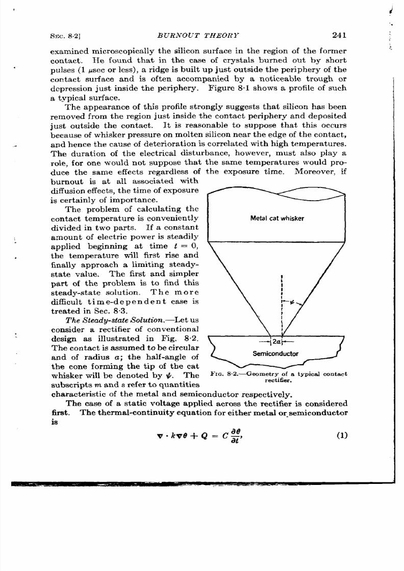
Sm . 8.2]
BURNOUT THEORY
241
examined microscopica lly th e silicon sur fa ce in t he region of t he for mer
contact.
He found tha t in the case of crysta ls burned ou t by shor t
pulses (1 ~sec or less), a r idge is built up just outside the per iphery of the
co~tact sur face and is often accompan ied by a not iceable t rough or
depr ession ju st in side
the per iphery. Figure 8.1 shows a profile of such
a t vpica l su rfa ce.
Th e appea rance of this pr ofile st rongly suggests tha t silicon has been
r emoved fr om th e region just inside th con ta ct per iph er y a nd deposit ed
ju st ou tside the contact.
It is reasonable
to
suppose tha t this occu rs
beca use of wh isker pr essu re on molt en silicon n ea r the edge of the contact,
...
a nd h en ce the cause of d et er ior at ion is cor r ela t ed wit h h igh t emper a tu r es
The dura t ion of the elect r ica l dkturbance, however , must a lso play a
role, for on e wou ld not suppose tha t the same tempera tures would pro-
duce the same effect s r ega rdless of
burnou t is a t all associated with
diffusion
effects,the
t ime of exposur e
is cer t ain ly of impor t an ce.
Th e pr oblem of ca lcu la tin g t he
con t act t emp r a tu r e is conven ien t ly
divided in two par t s. If a constant
amount of elect r ic p ower is st ea dily
applied beginning a t t ime t = O,
the t empera tu re will fir st r ise and
fina lly approach a lim it in g st ea dy-
sta te va lue. The fir st and simpler
par t of the problem is to find th is
st ea dy-st a te solu tion .
The more
difficu lt t ime-dependen t case is
t rea ted in Sec. 8“3.
The S t eady -stat e Solu t ion .—Let us
con sider a r ect ifier of con ven tion al
design as illust ra ted in Fig. 8“2.
Th e con ta ct is a ssumed t o be cir cu la r
and of radius a; the half-angle of
the cone forming the t ip of the ca t
wh isker will be denoted by IJ . The
su bscr ipt s m a nds r efer t o qu ant it ies
the exposu re t ime. Moreover , if
Met a lcatwhisker
FIG. S .2.—Geomet ry of a typ ica l con t act
rectifier.
ch ar act er ist ic of t he met al a nd sem icon du ct or r espect ively.
The case of a sta t ic volt age applied across the rect ifier is consi ered
fir st . Th e t herma l-con tin uit y equ at ion for eit her met al or -sem icon du ct or
is
V. W Q=C$
(1)
1

‘ f.
242 BURNOUT
where e is the t empera tu re above ambient
[SEC. 82
temperature,
k and C are the
appropr ia te thermal conduct ivit and thermal capacity per unit volume,
r espect ively, and Q is the power dissipa ted per un t volume.
For an ~‘
ohmic r esist an ce,
Q =
UIVV12,
(2)
wher e a is the elect r ica l conduct ivity and V the potential.
The equa t ion appropr ia te to the steady sta te is obta ined from Eq. (1)
by put t ing dO/&! = O.
Thus
v okve + u{V~12 = O.
(~)
It is convenient to regard the t empera tu re as the sum of two quant i-
..
t ies O, and o,, where 01 is the t empera tu re produced by hea t ‘genera t ed
in the bar r ier only and 9Zthe tempera tu re produced by dissipat ion in the
spread ing res is tance.
Let us fir st find &. From Eq. (3) it follows tha t
V.kvOl=O
(4)
out side the bar r ier r egion . If j is the thermal cur ren t density,
= –A-vt!llj
(5)
and from Eq. (4)
.
V.j =().
(6)
It is conven ient to draw an analogy to the case of the flow of elect r ic
current.
Thus, if i is the elect r ic cur ren t density, we have
i = —~v~
(7)
and
V.i=O.
(8)
The last two equat ions may be used to find the elect r ica l resistance,
bet ween t wo equipotent ia l sur faces of potent ia l differ en ce AV wh er e
I
s the
elect r ic cu r ren t . Simila r ly, the thermal resistance between iso-
t herma l su rfa ces wit h t emper at ur e differ en ce AO is
(lo)
where J is the tota l thermal cur ren t . Now the con tact is near ly an
equipotent ia l sur face since the elect r ica l conduct ivity of the met l
whisker is la rge compared with tha t of the semiconductor . If we assume
tha t the contact is an isothermal sur face, the two problems, elect r ica l

SEC.8.2] BURNOUT THEORY
243
and thermal, a re formally ident ica l and
u R~W = k rn ,h .ru ,.
(11)
By conservat ion of energy, the heat cur ren t J must be just equal
t o t he power P 1 dissipa ted in t he ba rr ier .
Let 0,, be the contact tempera-
tureresult ing from barr ier dissipa t ion only. Then,
0,0 = 61*ermP,. (12)
The thermal resistance ~,,.,~includesthe thermal resistances @, of the
semiconductor and & of the whisker . Since these arein para llel,
(13)
in the spreading resistance. We ust go back to Eq. (3) which is
sa tisfied by L92n the semiconductor ,
V . k,Vi3z+ U,IVV12 = O.
(14)
To solve th is equa t ion , a simplifying assumpt ion is made wh ich is not
exact ly cor r ect bu t probably a good approximat ion . It is assumed that
ez d epen ds on the coordina tes only through an explicit dependence on th e
potent ia l V. Thus,
Combining E qs. (7), (8),
which in tegra tes t o
e, = e2(v).
(15)
(14), and (15), it is easily shown that
()
d ~d~’ +1=0,
d~ u dV
(16)
o,= Av+B–
/
~ V dV,
(17)
L
where A and B are in tegra t ion constants.
If these constants can be
adjusted to fit the boundary condit ions on 02, the assumpt ion of Eq. (15)
is exact . This may be shown to be t rue in the limit as the thermal
conduct ivity km of the meta l whisker approaches either O or ~.
For
finite km it is only approximately the case. For boundary condit ions we
take
02=0
V=o
1
at a distance remote from the contact
(18a)
.,
V=vcl
~ ae
1 11
km ~
a t the contact.
(18b)
“i% *
m
244
BURNOU1’
[SEC. 82
Here n is a unit vector normal to the con tact sur face and the last condi-
t ion expresses the cont inuity of heat flow across the contact . In Eq. (17)
we in tegra te from
V = O
to
V = Vo
and assume
u / k
in depen den t of
tempera tu re and hence of potent ia l. From Eqs. (17) and (18), B = O
and
020= Avo – ;V;, (19
where oZ, is the contact tempera ture due only to dissipa t ion in the
spreading res is tance .
It may be shown that Eq. (18b) for deta iled continuity of hea t flow
across the contact is not str ict ly compat ible with our assumption, Eq.
(15), t a t & is, a fun t ion of the potent ia l only. If, however , the bound-
ary condit ion is expressed as an in tegral over the contact sur face, the
result is compat ible with Eq. (15). We get
~’%ls’~= WHm’~
(20)
Now, on the left side of Eq. (2o), we put
(21)
and we note that the r ight side of Eq. (20) is just the heat cur rent J ~
flowing through the meta l. y Eq. (10)
Thus, subst itut ing Eqs. (21) and (22) in Eq. (20) and put t ing
(22)
(23)
for t he e ect ric u rr en t wh en
R, is
t he (elect rica l) spr ea din g r esist an ce of
t he sem icon du ct or , we obt ain
( )
, do, v,
920
; 27 -*, “ ii = T.”
(24)
From Eq. (19), it follows tha t
()
e,
d—V _-
=A–; vo. (25)
,
Subst itut ing Eq. (25) in Eq. 24) and solving for A, we get
(26)

SEC.
82]
BURNOUT THEORY
245
Subst itut ing th is value of A in Eq. (19), we find
Now V~/ R . is the power P. dissipa ted in the spreading resistance and
a.R ,/ k . = C%is the thermal resistance of the semiconductor , by Eq. (11).
Thus
ezo= iPLRtherm ,
(28)
where 6t ,b_~ is the tota l thermal resis~ance given by Eq. (13).
The con tact tempera ture 00 due to heat developed both in the barr ier
and in the spreading resistance is 01, + 02,, or from Eqs. (12) and (28),
Oo=
LRtherm(waP,).
(29)
Our work so fa has been rest r icted to the case of a sta t ic voltage
applied across the rect ifier . If th is voltage is applied in the forward
direction,
P,>> P 1 at
volt ages requ ired for bur nou t; h en ce
do = @h .,u .P , (forwa r d dir ect ion )
(30)
where P is the total power dissipa ted.
In the blocking direct ion , P,
is
la rger t ha n P,.
If burnout is aused by igh-frequency alt rnat ing currents, our
result for the sta t ic case may be taken over direct ly since skin effect in
the semicond ctor is negligible even at the contact . This is proved in
Appendix B. In th is case, however , bar r ier dissipat ion plays only a
minor role. In the forward direct ion Eq. (30) st ill applies, and in the
rever se direct ion the barr ier capacitance shunts most of the curren t
a rou nd t he ba rr ier in to t he spr ea din g resi ta nce.
Th us, Eq. ( o) pplies
to burnout by microwave power .
Th e th erma l r esist an ce of t he semicon du ct or is obt ain ed dir ect ly fr om
Eq. (4.34) by subst itut ing the thermal conduct ivity k, for the elect r ica l
condu tivity u . We get
1
“ = 4k,a’
(31)
where a is the contact radius. The thermal resistance (R~ of the ca t
whkker is more difficu lt to est imate.
Th e calcu la tion of t emper at ur e
has so far been based on the assumption of a steady state, and the t ime
from the beginning of power applica t ion to the point where a steady
sta te is near ly a t tained has not yet been est imated. It will appear la ter
tha t the contact of average dimensions will reach a near ly steady tem-
pera ture after a t ime of about one microsecond. At this t ime, hea t from
the contact has not yet penet ra ted appreciably in to the cylindr ical par t
of the whisker stem; hen ce as far as the contact tempera ture is concern ed
246
the whisker is proper ly
BURNOUT
t rea t ed as an infin ite
[SEC. 8.2
cone. In th is case, it s
resistance maybe est ima ted by approximat ing its su rface by a one-sheet
hyperbola of revolu t ion asymptot ic to the cone. t s resist ance then
turns ou t to be
R. =
1
4k~a tan $/2’
(32)
where ~ is the half-a gle of the cone (see Fig. 8.1).
For t imes of 10-4 sec or longer , the resist ance of the cylindr ica l stem
of the cone must be added. This will be
1
am]... = —
(33)
uq2k~’
if no wax surrounds the whisker and
otherwise.
Here q is t he radius of the stem, p the r dius of the wax coa t ing, k . the
thermal conduct ion of the wax, and 1 the length of the stem. Equat ion
(34) was first der ived by Gant’ nder the assumption tha t the hea t
conducted by the meta l wire to its suppor t is small c mpared with the
hea t conducted away from the surface of the wire by the wax filler .
Although for very long times (severa l seconds) the effect of other
pa r ts of the ca r t r idge must a lso be considered, the discussion will for the
most pa r t , be rest r icted to t imes of the order of 1 psec or less.
Th e
steady-sta te solut ion is then given by Eq. (29) or Eq. (30) with R,b,,~
given by Eqs. (13), (31), and (32),
1
@~h .rm= 4a (k , + k - t an #/2)”
h’owz
k , = 0.2
cal
for silicon or germanium
sec-°C-cm
and
km = 0.4
for t ungs ten .
sec-°C-cm
If we take # = 30° and a = 10-3 cm,
00
F
= ~ (R = 100 °C/wat t
(35)
a nd is pr opor tion ally la rger for s,m aller r adii.
1D. H. T. Gant , ADRDE Resea rch Repor t No. 226, J uly 9, 1943.
2 This va lu o k. was det ermin ed by m ea su rem en ts m ade by K. a rk-H or ovit z
(private communicat ion).
SEC.8.2]
BURNOUT THEORY
A circu lar contact has been assumed in
d
247
i
t hese ca lcu la t ions. In
Appendix C, it is proved tha t the semiconductor resist ance offered by an
ellipt ica l con tact of semiaxes a and b(a > b) is
K
“ = 2uk .a’
(36)
where K is the complete eh ipt ic in tegra l of the fir st kind with modulu
k=~~. Ifa>>b,
Kzlnk?
b
(37)
If t he ca t wh isker in th is case is assumed to have the shape of a wedge
of ha lf-angle ~, it s resistance can be shown to be about
K
~ = 2uk .a tan $/ 2”
(38)
The tot a l therma l resistance can then be made very small by making
a la rge. On the other hand, the rect ifying proper t ies of such a con tact
should be comparable to those of a cir cu lar con tact of radius equal to th
shor t semiaxis b In Chap. 4 r ect ifica tion and con ver sion efficien cy er e
found to depend on the product
uCR.,
whe e u is 2T X fr equ en cy, C is t he
ba r r ier capacitance, and R. is the elect r ica l spreading resistance. The
a rea of t he ellipt ica l con ta ct is Tab a nd so it s ca pa cit an ce [see Eq. (4.17)] is
c’ = ~! (39)
where D is the th ickness of the ba r r ier layer and c the permit t ivity of the
semiconductor . Thus, for a long th in con tact ,
. and for a circu la r contact of radius b,
(40)
(41)
These quant it ies a re of the same order for the same b even for fa ir ly
la rge ra t ios of a to b. Thus a lon g th in cont ac has t he desirable pr oper ty
of being able to withstand larger power dissipa t io , yet st ill give good
per formance as a rect ifier or conver t er . Unfor tuna tely it has not yet
been possible t o ma nu factu re cryst als with such con ta ct s. The difficu lty
ar ises from the fact tha t the eccen t r icit y of the con tact ellipse must be
very la rge for the effect to be pronounced. As an example let us con-
power-handling
[SEC. 8.3
capacity
248
BURNOUT
sider the ellipt ica l con tact with wice the
of a cir cu lar con ta ct of radius d.
Th e su pposit ion is t ha t t he t wo con ta ct s
a re equ ally good r ect ifier s, h en ce uCR, is the same for each .
Th e r esu lt
is tha t the ellipt ica l con tact must have it s long semiaxis a = 6.66 and
its shor t semiaxis b = 0.3ci and thus a/ b = 22. Such a con ta t is
d ifficu lt t o con st r u ct .
An a lterna t ive is to const ruct a rect ifier with a number N of small
rect ifying con tayts. If the separa t ion of neighbor ing con tacts is la rge
compared with the diameter of a con tact , the product
wCRS
for t he wh ole
rect ifier is just the same as for an individual con tact . On the other
hand, the thermal re ist ance 6it i_ will decrease inversely with N. An
improvement in burnout of a factor of 2 cou ld be achieved with on ly two
para llel contacts. This is perhaps easier to const ruct than a single very
lon g t hin con ta ct .
8.3. Bu rn ou t Th eor y. Contact T em perature as a Function of T irne.—
The th eory in the preceding sect ion applies t o the st eady-sta te solu t ion
of t h e t herma l-con t in u it y equ at ion .
As will appea r la ter , th is solu t ion is
not va lid if the t ime elapsed since the applica t ion of power is less than
10@ or 10–7 se . Since burnout is now believed to be usua lly the resu lt
of very shor t pulses of the order of 10–9 or 10–8 sec in dura t ion , it is
obviou sly impor t an t t o examine t he solu t ion for t hese cases.
If t he t ime is so shor t tha t no hea t has appreciably diffused away
from the loca lity where it was genera t ed, the t empera tu re is given by the
amount of hea t genera t ed per unit volume divided by the thermal capac-
ity C per unit volu e, or
/
1’
‘=E ~
Q dt,
(42)
wher e Q is the ra t e of genera t ion of hea t per unit volume. This resu lt
can be direct ly obta ined from the the mal-con t inuity equat ion [Eq. 1)]
by suppressing the conduct ion term v . lcvO. Difficu lt ies ar ise, however ,
if an a t t empt is made to apply Eq. (42) t o the usua l con tact between the
meta l c t whisker and the semiconductor . It tu rns ou t tha t Q becomes
infin ite a t the per iphery of the con tact because of the crowding of lines of
cur ren t flow; Eq. (42) would then predict an infin ite t empera tu re there,
wh ich is, of cou rse, a bsu rd.
The t rouble is tha t it is not r igh t to suppress the conduct ion term in
Eq. (1) nea r a singula r ity in Q. At the per iphery of the contact th ere
is no t ime t so shor t tha t conduct ion can be neglect ed. Equat ion (42)
sh ou ld h old well, h owever , a t dist an ces r om t he edge la rge compa red wit h
the radius of the con tact . Clea r ly a separa t e invest iga t ion of the t emp-
era tu re near the per iphery is necessary. To do th is we must fir st find
ou t how Q, the hea genera t ed per unit volume, depends on posit ion ,
espe ia lly n ea r t he per iph er y.

SEC. 8.3]
BURNOUT THEORY
249
The potent ia l dist r ibu t ion in the semiconductor must fir st be found.
The contact a rea , circu la r inshape, will reassumed equipoten t ia l. It is
con ven ien t t o in tr odu ce sph er oida l coor din at esin t he followin g wa y.
Figure 8.3 shows a sect ion th rough the cen ter of the con tact conta in -
ing the axis of symmetry. The or igin of r ctangula r coordina t es (z,y,z)
is t aken at the cen ter of the con tact ; the plane z = O is coincident with
t he con ta ct su rfa ce a nd t he posit ive x-dir ect ion is in to t he sem icon du ct or .
Spheroida l coordina tes & f and Q
are defined in such a way hat Q
~P=(v2+,2)’f4
is t he lon git ude a ngle;
‘.
+, + ‘2
az(l + ~z)
and
0.6
0.8
–~ ‘2
I
= 1 (44)
az~z
az(l – <2)
It=l
I
define ~ and ~. Here pz = yz + Z2.
Equat ion (44) is the equat ion of a
;
x
family of on e-sh eet h yper boloids
FIG. S .3 .—Sect ion through the contact show-
of revolu t ion and Eq. (43) is the
ing coord ina te sys tems used .
equa t ion of an or thogona l family of obla te spheroids, a par t cu la r mem-
ber of which ~ = O, is a fla t disk of radius a coinciden t with the con t ct
sur face. Since the contact su r face is equipoten t ia l, the poten t ia l V will
be assu ed to depend only on {. Laplace’s equat ion for V isl then
;(l+{’):; =O.
(45)
In tegr at in g, we obt ain
V = A tan-’ ~ + B,
(46)
where A and B are in tegr at ion con st an ts. Ifwetake V= VOat~=~
and V = O at the cont ct ( = O), we obta in
V = VO~ tan–l {.
(47)
To find Q we must find vV, which is2 given by
1See, for examp le, W. R. Smyt he, S t atic an d Dyn am ic E lect ricit y, 1s t ed,, h’IcGraw-
Hill, 1939, Sec. 5.27.
ZIbid., S ees. 33 and 5.27.

250
BURNOUT
[SEC.8.3
and from Eq. (2), he heat genera ted per unit volume is
4v&l
Q=—
1
rzaz (1 + {2) (~2 + ~z)
P
(49)
= 7%3(1 + (*)($* + P)’
where P is t he tota l power VO/ R , dissipa ted in t he spr ea din g r esist an ce;
R, = l/4ua. As an auxilia ry coordina te r is in t roduced as the distance
from th e per iph ery to some poi t (x,P) in t he semiconductor . Evident ly,
rz = X2 + (p — a )z.
(50)
Solving Eqs. (43) and (44) for z and p, subst itu t ing in Eq. (50) and using
the approximat ion , { = O and ~ = O, we find
f = ; (rz + t’).
(51)
For (
=Oandf
= O, we find from Eqs. (49) and (51)
Q
=
Thus Q is observed to approach cc
)
Metalcatwhisker
Surfaceof
eemi.conductor
\,/
“
F IQ. S.4.—Pola r oor din a tes (r , d) of a
gener ic point (p) nea r the edge of the
contact.
P
27r2a2r”
(52)
as r approaches zero.
With thk expression for Q we
may now solve the thermal-con-
t inuity equat ion for poin ts nea r th e
per iphery (r << a). In this region
the curva ture cf the per iphery may
be neglected and the edge of the
contact may be ta!:en as a st ra ight
line. Our coordina tes are r and ~,
the polar angle, as illust ra ted in
Fig. 8.4. The surface of the meta l
cone makes an angle
00
with the
extension of the surf~ce cf the
semiconductor.
If it is assumed tha t k is in de-
pendent of posit ion , the thermal-
con tin uit y equ at ion n ow becomes
kV20+Q=C$
(53)
where
Q=o
in the meta l (m < @ < 40),
Q.L
2r2a2r
in the semiconductor (O < + < m),
a nd t he La pla cia n
1
(54)
v2=:2+; ;+l_a_2.

SEC. 8.3 ]
BURNOUT THEORY
251
Th e pu lse power P is assumed con sta nt (fla t pulse) and dissipa t ion in t he
bar rier la yer n eglect ed. Th e resu lt s should apply t hen eit her t o d-c power
in t he forwa rd (con du ct in g) dir ect ion or t o m icr owa ve power .
S ince only
or der of m agn it ude is desir ed, k and C are, for simplicity, assumed to be
t he same in meta l and semicon du ctor a nd a re indepen den t of t emper atu re,
and +0 is assumed to equal 27.
These approxima t ions in t roduce lit t le er ror . The fina l r esu lt is
expressed as the ra t io of the t empera tu re a t some poin t on the con tac
t o the equilibr ium va lue of th is t empera tu re. This ra t io depends only
on t h e t h erma l diffu sit ivit y, K = k / C, which is about the same in silicon
and tungsten . Also the assumpt ion 00 = 2m is not fa r from the t ru th ,
since the whisker tends to mushroom out a t the edge of the contact .
The solu t ion of Eq. (53) is desir ed tha t sa t isfies the. oundary condi-
tions:
ae
a t~=Oor2ir , —=0;
a~
at r=~, 0=0;
a t t=O, 0=0.
I
(55)
The “requ ir ed solu t ion may be found by the usua l methods.
For poin ts on the con tact su r face (O = r) the solu t ion reduces to
‘ = p & [ 4 9El’
(56)
where K =
k / C is t he t herma l dMfu sivit y, a nd
In(x) is t he modified Bessel fun ct ion of or der n , tha t is, In(z) = j-”.J .(jz).
For T2/8K~ <<1,
and for r2/8d >> 1,
e
1 Pt
— — .
= C 4u2a2r
(58)
(59)
This last r esu lt is exact ly tha t given by Eq. (42), since by Eq. (52)
P/ (4u2a2r) is one-ha lf the ra te of evolu t ion of hea t per un it volume in the
semiconductor a t a dist ance r from the con tact edge.
The factor + is
expla ined by the fact th t the tempera tu re has been eva lua ted on the
con tact su r face. Since no hea t is genera t ed in the meta l and an amoun t
Q per unit volume is genera t ed in the semiconductor , t he average va lue
H is effect ive on the su r face.
Th e gen er al ch ar act er of t he t em per at ur e-t im e r ela tion is n ow eviden t.
For any poin t nea r the edge, but not actua lly on it , t he t empera tu re is
propor tion al t o t he en er gy dissipa ted, n amely, W = Pt, for sufficient ly
252
BURNOUT
[SEC. 83
sh or t t im es.
As the t ime increases, the tempera ture rises ess swift ly,
even tu ally becom in g pr oport ion al t o t he squ ar e r oot of t he t ime. Accor d-
ing to the presen t solut ion the tempera ture should cont inue to increase
without limit . The reason this ca tastrophe does not occur is tha t th is
solu t ion holds only provided the heat evolved in the semiconductor has
not had time to diffuse over a distance comparable with the contact
dimensions. For longer t imes (t > U2/K) the neglect of the curvatu re of
the contact per iph ery is no longer va lid.
Th e gen er al qu alit at ive r esu lt
is t hen
t <<:,
Oapt=w
(60)
(61)
(62)
In the last case o is given by Eq. (30) for t = 1 psec.
In Fig. 8.5 the tempera ture i plot ted in units of the steady-sta te
tempera ture, Eq. (30), as a funct ion of the t ime for a number of values
of r . Equat ion (35) has been
used for (R,he_ in Eq. (30) and, in
accordance w i t h o u r presen t
assumption, k = a = k% and
~ = 90°. This gives, for the
s teady-s ta t e t empera tu re,
In plot t ing these curves a has been
put equal to 10-3 cm, which [is
appropr ia te to a fa ir ly large con-
tact , about tha t used for high-
burn ut crystals designed for the
10-cm band. It should be noted
tha t 0/80 is propor t ional to I a.
Also,
K has been taken eaual to
t (see)
L
FIC. 8.5.—Cont act tempera t ur e 6 at a
0.54 cmz/see, wh ich is t he mean
poin t n ea r t he per iph er y as a fu nct im of t he
of the va lues of K for tungst en
t ime s ince power was applied .
(K = 0.62 cm’/sec) and for silicon
(. = 0.46 cm2/see). The ra t io 0/00 depends on k and C only through
K = k/C, hence separa te va lues need not be assumed for them.
The dashed line in Fig. 8.5 is a plot of 13q. (59) for t he t empera tur e-
t ime rela t ion at t he cent er of the contact .
This equa t ion holds only for
SEC. 83]
BURNOUT I’IIEOR Y
253
small t imes (t << a2/K), but it has been ext rapola ted to the equ libr ium
temperature.
hese curves should apply up to t imes o the order of a2/K ( = 10-6 sec
in our example) or , equiva lent ly, they apply provided 0/00 <<1. The
solut ion for longer t imes is probably like tha t given by the broken line in
Fig. 8.5. The t~mpera ture ~hould
reach an equilibr ium value at
about 5 X 10⁻⁶ sec for a con tact
of th is size (10–6 cm radius). For
a con tact of average size the t i e
requir d for the steady sta te is
closer to 1 X 10-o sec.
An interest ing result of th is
analysis is tha t a t first the tem-
pera ture r ises much more rapidly
a t he edge than near the cen ter
of the co tact . In Fig. 8.6 the
tempera ture is given as a func-
t ion of the distance r from the
I I
I 1
edge of the con tact for a number
‘“’~o-’
o-, ~o-,
of t ime in tervals. For any t ime
in ter va l t he t emper at ur e is a maxi-
FXG. 8.6.—Con ta ct t emper a t ur e O nea r
mum at the edge and decreases
t h e per ipher y a s a funct ion of d ist a nce r fr om
as T increases. As the t ime in-
periphery.
creases, the tempera ture at any point increases and, as a funct ion of r , is
fa ir ly constant Up to about r = fi, beyond which it star ts to drop off.
These results a re qualita t ively in accord with the observa t ions of
Pfann (see Sec. 8.1) and expla in why F’farm observed deter iora t ion of
only the edge of the contact for shor t pulses (up to 10–6 sec dura t ion),
whereas for long pulses (severa l seconds ciura t ,ion) the whole contact a rea
is affected. The suggest ion has been made that edge burnout may be
due to skin e fect at the contact , but in Appendix B it is shown that the
di feren t ia l hea t ing between edge and center caused by skin effect is
negligible a t all microwave fr equencies.
Fur thermore Pfann finds the
same effects for shor t d-c pulses (up to 10–6 see).
Tendency to edge burno t is aggrava ted by the fact that at above
700”C the conduct ivity of silicon increases rapidly with tempera tur
because of excita t ion of elect rons from the filled band to the conduct ion
band (see Sec. 3.1). These tempera tures will be reached fir st at the edge
of the contact , and the resu lt ing increase in conduct ivity there will
increase the flow of curr en t near the edge rela t ive to tha t at the center
of the contact .
Since all par ts of the contact a re effect ively in parallel,
an increase in condt ict ivity of the edge rela t ive to the rest of the contact
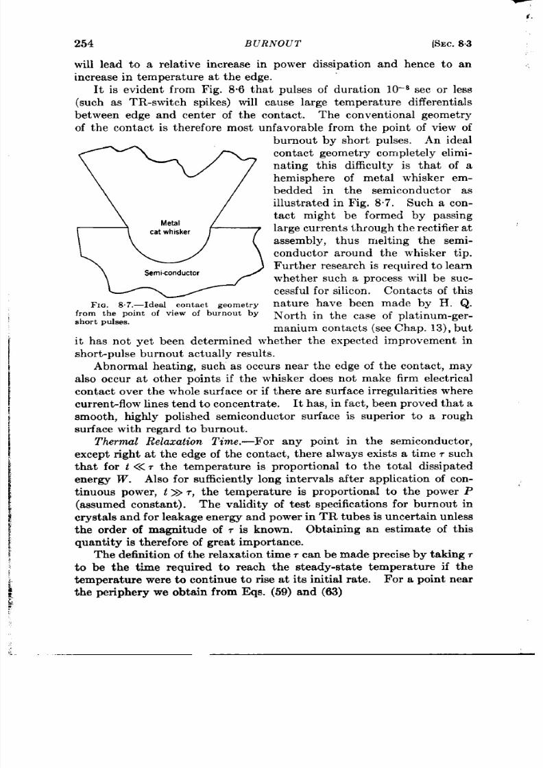
254
BURNOUT
will lead to a rela t ive incre se in power
increase in t empera tu r a t the edge.
~
i.
[SEC.8.3
dissipa t ion and hence to an
It is evident from Fig. 8“6 tha t pul es of dura t ion 10–8 sec or less
(such as TR-switch spikes) will cause la rge tempera ture differen t ia ls
between edge and cen ter of the contact . The conven t iona l geome ry
of the con tact is therefore most unfavorable from the poin t of view of
F IG. S.7.—Idea l cont act geom et ry
from the point of view of burnout by
shor t pu lses .
burnout by shor t pulses. An ideal
con ta ct geom et ry complet ely elimi-
na t ing th is difficu lty is tha t of a
hemisphere of meta l wh isker em-
bedded in the semiconductor as
illustra ted in Fig. 8.7. Such a con-
tact might be formed by passing
large cur ren t s th rough the rect ifier a t ‘
assembly, thus melt ing the semi-
conductor around the whisker t ip.
Fur th er resea rch is requ ir ed t o lea rn
whether such a process will be suc-
cessfu l for silicon . Contacts of this
na ture have been made by H. Q.
Nor th in the case of pla t inum-ger -
manium con tacts (see Chap. 13), but
it has not yet been determined whether the expected improvement in
sh or t-pu lse bu rn ou t a ct ua lly r esu lt s.
Abnormal hea t ing, such asoccurs nea r the edge of the contact , may
also occur a t other poin ts if the whkker does not make firm elect r ica l
cont act over th e wh ole sur face or if t her e a re sur fa ce ir regular it ies wh ere
cu r r en t -flow lin es t end t o concen t r at e.
It has, in fact , been proved tha t a
smooth , h ighly polished semiconductor sur face is super ior to a rough
surface with r egar d t o burn out .
T herm al R elaxation Time.—For any poin t in the semiconductor ,
except r ight a t the edge of the contact , t here a lways exist s a t ime r such
tha t for t <<7 the t empera tu re is propor t iona l to the tota l dissipa ted
energy W. Also for sufficien t ly long in terva ls a fter a plica t ion of con- ,
t in uou s power , t>>T,the t empera tu re is propor t iona l to the power P
(assumed constan t ). The validity of test specifica t ions for burnout in
crysta ls and for leakage energy and power in TR tubes is uncer ta in unless
the order of magnitude of r is known. Obta ining an est imate of this
qua nt it y is t her efor e of gr ea t impor ta nce.
The defin it ion of the relaxa t ion t imer can be made precise by taking r
to
be the t ime requir d to reach the steady-sta t e t empera tu re if the
tempera tu re wer e to cont inue to r ise a t it s init ia l ra t e. For a poin t nea r
the per iphery we obta in from Eqs. (59) and (63)

SEC. 8.3]
BURNOUT THEORY
255
(64)
I
of t he cont act we have, from Eqs. (42) nd (49), since { = O and ~ = 1
at t he cen t er ,’
Pt
00 = 27r2asC
t << T ).
With Eq. (63) th is gives for ra t the center ,
Evidently,
( )
n = 2TC ~ (r<< a).
a
(65)
(66)
(67)
The relaxa t ion t ime is seen to depend linear ly on the distance r from the
edge of t he con ta ct .
What effect ive value of r should be used to obta in a value of, appro-
pr ia te to the whole contact is difficult to decide. As a guess let us take
10-s cm < r < 10–4 cm.
Then, if a = 10–a cm and K 0.54 cm2/see,
TC= 2.3 X 10–C see,
(68)
and
4.6 X 10_8 sec < 7P <4.6 X 10⁻⁷ sec.
(69)
It should be noted that r , is propor t ional to the first power , and r . to the
square, of the conta ct radius.
The predominant cause of crysta l burnout in pract ice is believed
to be the TR-switch spike, which has a dura t ion of about 2 to 3 x 10 0
sec. Since th is per iod is shor ter than our lowest est imate or ~p it is
probably the energy of the spike ra ther than its peak power that is effec-
t ive in burnout . However , this reasoning applies to a contact of la rge
dimensions (a = 10-8 cm), appropria te to high-burnout 10-cm band
rect ifiers. For a l-cm and rect ifier a = 10–4 cm and Tp may be smaller
;b
than the spike dura t ion .
At present , it is ahnost universal pract ice to assess the protect ion
offered by TR tubes by the amount of leakage spike energy. The pre-
ceding considera t ions indicate tha t th is protect ion may not be adequate
for crysta ls of small contact dimensions. Our est imate of r , i , however ,
only a guess since the effect ive value of r is unknown.
In the next
1The
factor
2 in the denominatorof Eq. (65) is requiredbecause 130s the contact
t empera tu re. In the meta l whiskerno hea t is developed ; in the semiconductor the
hea t-developedQ is given by E q. (49); a t the contact the meanvalue Q/2 applies .
256
BURNOUT [SEC. 8.4
sect ion some exper imen ts a re descr ibed which in dica te t hat t he effect ive
relaxa t ion t ime for 1N21 rect ifiers (con tact radius 2 or 3 X 10⁻⁴ cm) is
about 10-s sec.
In the case of crysta ls designed for use as video detectors, no TR
switch is used; urnout is caused by pulses of the order of 10-o see;
hence the theory of the steady-sta te t empera tu re applies, and it is the
power ra ther than the energy of the pulse that is important .
8.4. Experiments on Burnout .-In this sect ion some exper iments a re
descr ibed which throw light on the na ture of burnout and make possible
an est imat ion of some of the constants involved in the theory out lined in
Sees. 8.2 and 8.3.
Burnout by Cont inuous D-c Power .—In 1942 some carefu l work was
done by Lawson and his collabora tors a t the University of Pennsylvania’
on burnout as a result of the applicat ion of cont inuous d-c power under
carefu lly cont rolled condit ions .
A silicon cube about 5 mm on a side cut from an ingot obta ined from
t he Bell Teleph on e La bor at or ies was pla ted with iron on one si e and
mounted on a lead matr ix with the pla ted side in contact with the lead.
Next , the sur face opposite the pla ted side was ground and polished to a
mir ror finish, then etched with hot NaOH solut ion before each burnout
test . Following th is, the cube of silicon with its mount ing was placed
inside a bell ja r on table. A shor t st raight piece of 7-roil tungsten wire
was ca refully poin ted and ounted in a pin vise and ar rangements made
to press the poin t with a controlled and known force aga inst the silicon
sur face. No tapping was used. The d-c character ist ic, especia lly in
the forward direct ion,
was
found to be remarkably reproducible when
different poin ts were pressed with the same for ce on differen t par ts of the
surface. Fur thermore, it was found tha t the area of the con tact sur face,
as determined by microscopic measurements of the diameter of the
squashed poin t after removal, was defin itely rela ted to the force with
which the poin t had been pressed against the surface. The radius of the
poin t could then be ascer ta ined from a knowledge of th is force and of
the force -a rea rela t ionsh ip .
A fa ir ly defin ite a lthough ra ther art ificia l cr iter ion for burnout was
established. It was discovered tha t the resistance R1 of t he r ect ifier
at 1 volt in the rever se direct ion depended on the mount of over load
power
P
previously applied in either direct ion . This resistance RI a t
first increased with the over load, reached a maximum, and thereaft er
decreased sharply. A contact was deemed “burned out” when th is fina l
sharp decrease occur red. It was la ter established tha t the conversion
1A. W. Lawson et a l., “DC Burnout Tempera ture in Silicon Rect ifie rs,” NDRC
14-113,Univ. of Penn., Nov. 1, 1942.
&

SEC. 8.4]
EXPERIMENTS ON BURNOUT
257
efficien cies of ar tr idge r ect ifier s tha t had been “bur ned out ” in th is way
were defin it ely deter iora ted .
Three methods wer e used to find the t empera ture at the contact at
bu rnout . In the fir st method the tempera tu re was measured with a
thermojunct ion welded to the cat wh isker abou t 1 mm from the con-
t act . This device dld not direct ly measure the tempera ture a t the
con tact and had to be calibra ted by hea ing the whole cube of silicon up
to a known tempera tu re and compar ing this t emperatu re with the emf
of t he thermocouple.
These measur ements indicat ed that t he tem per a-
tu re a t burn ut was 500° ~ 100 C.
In the second method the amount of over load power recwired to reach
the burnout point was measured as a funct ion of the base temperature
of the silicon block. After each measurement the probe was removed,
the silicon surface etched and a new contact of the same dimensions was
formed and tested at a higher base temperatu re in the forward direct ion .
The power required for burnout was found to decrease linear ly with the
base tempera tu re of the block (which was ra ised as high as 300”C). By
extrapola t ion of this st r a ight line it was found that , a t a t emperatu re of
490”C, no power would be requ ired for burnout . The presumpt ion is
then that 490°C is the burnout t empera tu re of the con tact .
The third method made use of the results of the theory of Sec. 82.
According o Eqs. (29) and (35) the steady-sta t e con tact t emperatu re is
given by
*P , + PI
0 4a(lr l + k, tan ~/2)’
(70)
where P. is t he power dissipa ted in t he spr ea din g r esist an ce, PI t he power
dissipa ted in the barr ier , a the radius of the con tact , kl and k , t he t herma l
conduct ivit ies of the semiconductor and whisker , and # the half-angle of
the conical whisker t ip. This equat ion was applied to burnout b power
applied in the forward direct ion here P1 = O and P, = IZR,, where I is
the elect r ic cur rent . The equat ion was also applied to the case of power
in the r ever se direct ion , wher e P 1 = 12R 1 and P = 12R, and R 1 is the
barr ier resist ance. Th e spr eading resist ance R, was measured fr m the
forward cur ren t -volt age character ist ic an th bar r ier resistance in
t he ba ck dir ect ion RI was taken to be the difference between the tota l
r esistance and R,.
When proper accoun t was taken of Pelt ier heat
(which is abnormally large in semiconductors) the tempera tu re a t burn-
ou t given by Eq. (70) was found to be the same, within exper imen ta l
er ror , ir respect ive of t he dir ect ion of t he applied over load volt age; it was
equal to 470° + 40”C. The Pelt ier heat accounted for an increase of
30°C in the calcula ted tempera tu re for forward burnout and a decrease
of the same amount for back burnout .
The final resul is in good
accord with the direct ly measured burnout t empera tu re.
Th is a gr ee-

258
BURNOUT
[SEC. 84
ment , however , is somewhat m rred by the fact tha t two er ror s were made
in the ca lcu la t ion . These er ror s a re in opposite direct ions and it is not
unlikely that they almost cancel.
One er ror involved using a va lue of
k, one-half the presen t ly accepted va lue (0.84 wat ts/cm-°C), and the
other er ror resu lted from neglect of the therma resistance of the cylin -
dr ica l whisker stem. As shown in Sec. 8.2 th is neglect is va lid for pulses
of 1 psec dura t ion or less, but in the presen t case of con t inuous power the
st em r esist an ce ca nn ot be n eglect ed.
It can be shown that the two er ror s
would c ncel if the stem of the probe had a length of 3.3 mm. The
actua l length was somew at longer than th is but , if radia t ion effects a re
a llowed for , the effect ive length might well have been abou t 3 or 4 mm.
Some genera l fea tu res of the theory were confirmed in these invest i-
ga t ions. For example, from Eq. (27) it is noted tha t for the sa e applied
for wa rd volta ge VOt he con ta ct t empera tu re is indepen dent of t he con ta ct
radius. Lawson et al. found tha t burnout occu rred at the same forward
voltage, 6.6 + 0.7 volts, regardless of the force pressing the whisker
against the silicon and consequen t ly regardless of the con tact radius.
In the rever se direct ion , the volt age requ ired for burnou t depended on
th e applied for ce, as is t o be expected, con sider in g th e effect of t he bar rier
layer , but the burnout tempera tu re according to Eq. (70) was found to
be ,approximately independen t of the force and hence of the contact
radius.
Burnout by S hort D-c Pulses. —According to the theory of Sec. 83
there should exist a t ime ~ such tha t , for pulse dura t ions small compared
with T, the con tact tempera tu re is p opor t iona l to the energy W of the
pulse and does not depend ex licit ly on its dura t ion . On the other hand
un iform pulses of dura t ion long compared with 7 should result in a con-
tact tempera tu re propor t iona l to the power P of the pulse. In Sec. 8.3
we defined r to be the t ime requ ired to a t ta in the steady-st a te tempera-
tu re if the tempera tu r con t inued to r ise a t its init ia l ra te. An a lterna t ive
defin it ion is obt ain ed on t he followin g basis:
for pu ls du ra tion t<<T,
O = AW = APt ,
(71)
and for t>>T
~= Bp_BW,
t
(72)
where A and B a re propor t iona lity constan ts. Let us plot the energy W
requ ired to produce a cer ta in defin it e deter iora t ion of the rect ifier
against t he pu lse du ra tion t. The result ing cu rve should have the gen-
era l appearance of the solid curve of Fig. 8.8. The requ ired pu lse energy
W should be constant for small
t
and propor t iona l to t for ong
t. Th e
in tersect ion of these two asymptotes of the curve defines a t ime r which

SEC. 8.4]
EXPERIMENTS ON BURNOUT
259
can be called the relaxa t ion t ime of the contact .
It is easily seen that
th e two defin it ions of r are equivalent provided th e amount f deter iora-
t ion is determined by the contact tempera tu re and not by the t ime.
In or der t o measu re r a ccor din g t o this secon d definit ion t he following
exper iment was performed, using an appara tus shown schematica lly in
F ig. 9.35. A coa xia l-line con den ser of a djust able len gth
1
and cha ra ct er -
ist ic impedance ZO was charged b a d-c supply to a known voltage V.
By means of the switch S the con-
den ser cou ld be qu ic ly con nect ed
to the terminals of a crysta l rect i-
fier , which would then terminate
the coaxia l line. If the impedance
of the rect ifier matches th e line im-
peda nce 20, a sin gle pu lse of magn i-
tude V/2 and dura t ion 21/c, where
c is the velocity of light , is applied
to the rect ifier . The energy dis-
sipated in the rect ifier is equal to
t he ot en tia l en er gy of
the condenser before discharge.
Here C is the capacitance of the
1/ I
/
/
I
0
T
t—
Pulseduration
FIG. S.S.—Pulse energy W required
for
a given d et er ior at ion a s a fu n ct ion of p ulse
du rat ion t .
coaxia l line.
If t he r ect ifier r esist an c R does n ot match th e line imped.
ante, a succession of pulses each of dura t ion 21/c and of decreasing
amplitude re ults; but if
~Zo < R < 2Z0,
90 per cent or more of the tota l available en ergy +CVX will be dissipated
in th e first pulse.
Th e exper im en ta l pr ocedu re wa s a s follows:
1. A number of silicon rect ifiers of standard type, all made by the
same manufacturer , were collected and divided arbit ra r ily in to
groups of 10. The loss and noise tempera tur of each crysta l was
measured and th e noise figure
F of a receiver with an amplifier of
5 db noise figure was ca lcula ted from these data for each crysta l.
The mean value of F was found for each group of 10 crystals.
2. The coaxia l line charged to a given energy and adjusted to a given
length was discharged in to one group. After remeasurement of F,
the same group was exposed to a pulse of higher ener~ and again
remeasured. This procedure was cont inued until the average
det er ior a tion in F was more than 6 db.
3. The process outlined in (2) was applied to a second group of unit s
with the sole difference tha the line length was increased by a
fa ct or of a pproxima tely 2.

260
BURNOUT
[SEC.85
4. The process was repea ted ~~ith the other groups successively,
increasing the line length and therefore the pu lse dura t ion by a
factor of about 2.
A large amount of data was recorded, but the genera l resu lt , is well
r epresen ted by the data giving the amounts of energy and power requ ired
to produce an average deter iora t ion in F o 3 db. These data a re given
in Table 8.1.
TABLE 8,1.—PuLsE ENERGYH’ ANDPOWERF’ REQUIREDFOR3-DB DETERIOIIATION
IN NOISE F IGURE AS A FUNCTIONOF PULSE DURATION~
T (see X 10-’)
2.3
3.9
7.0
13.0 26.0
W (ergs)
0.76 0.81
0.61 0.50 1.49
P (watts) 33 21
8.7 3,8
5.7
As is eviden t fr om t he t able, t he en er gy r equ ir ed for 3-db det er ior at ion
for shor t pulses is near ly independen t of pulse dura t ion but increases
sharply a t t = 2.6 X 10–s sec. On the other hand the required pulse
power P decreases with pulse dura t ion at fir st and becomes roughly
constant a fter t = 1.3 X 10⁻⁸ sec.
The relaxa t ion t ime appea rs, there-
fore, to be about 1 or 2 X 10-s sec.
In th is exper iment , the impedance of the coaxia l line was 50 ohms,
its capacitance per cen t imeter of length was about 1 ppf, and a pulse
energy of 1 erg cor responded to a charging voltage of 90 volt s for the
shor test length used. The voltage was app ied to the cr sta l in the
forward direct ion ; it may be assumed tha t , a t the high voltages used,
t he r esist an ce of t he crysta l is t he spr ea din g r esist an ce of t he sem icon du c-
tor , which for the crysta ls used was between 25 and 50 ohms.
In these exper iment s only one pulse was applied at each power level.
It is known that smaller energies and powers are required for the same
deter iora t ion when mult iple pulsing is used, but the available data bear -
ing on th is poin t are not extensive.
Accor din g t o r epor ts fr om Engla nd
the energy per pulse required for a given deter iora t ion is less by a factor
of 3 to 5 for 106 pulses than for a single pulse.
Th e pu lse r epet it ion
frequency in th is work was 100 pps.
It was established at the Radia t ion Labora tory tha t aft er one pu lse
causing apprecia ble det er iora tion th e effect of a similar addit ion l pu lse
is negligible, but tha t 109 addit ional pulses of the same energy almost
doubles the deter iora t ion of the fist . Aft er th is, st ill fu r ther pulses
(104) of the same energy may either produce st iU more deter iora t ion or
may have lit t le addit ional effect , depending on the unit tested.
8.5. Burnou t Lfi a t ions of Standsrd Crysta l Units.-The following
est imates of burnout limita t ions of standard crysta l units must be
rega rded as crude.
As men t ioned above, there is a decided lack of
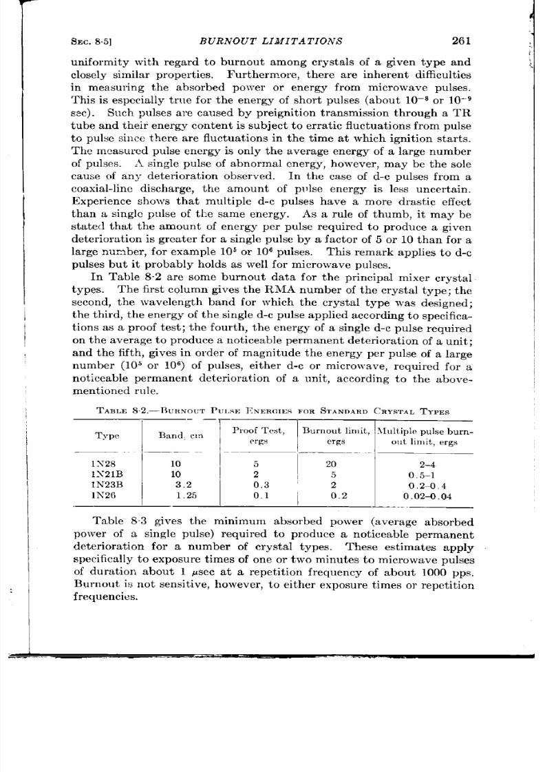
I
I
I
I
SEC.
BURNOUT LIMITATIONS
261
uniformity with regard to burnout among crystals of a given type and
closely similar pr oper ties.
Furthermore, there are inheren t dlficult ies
This is especia lly t rue for the energy of shor t pu lses (about 10-6 or 10-9
see). Such pulses are caused by preign it ion transmission through a TR
tube and their energy conten t is subject to errat ic fluctuat ions from pulse
to pulse since there are fluctua t ions in the t ime at which ignit ion star ts.
The measured pulse ener y is only the average energy of a large number
of pulses. ii single pulse of abnormal energy, however , may be the sole
cause of any deter iorat ion observed.
In the case of d-c pulses from a
coaxia l-line discharge, the amount of plllse energy is less uncerta in .
Exper ience fihows that mult iple d-c pulses have a more drast ic effect
than a single pulse of the sa e energy. As a ru le of thumb, it maY be
stated that the amount of energy per pulse required to produce a given
det er iorat ion is grea ter for a single pulse by a factor of 5 or 10 than for a
large number , for example 10s or 106 pulses. This remark applies to d-c
pulses but it probably holds as well for microwave pulses.
In Table 8.2 are some burnout data for t he pr incipa l mixer crystal
types. The first column gives the RiMA number of the crystal t ype; t he
second, the wavelength band for which the crystal t ype was designed;
the th ird, the energy of the single d-c pulse applied according to specifica -
t ions a a proof test ; the four th , the energy of a single d-c pulse required
on the average to produce a not iceable permanent deter iora t ion of a unit ;
and the fifth , gives in order of magnitude the energy per pulse of a la rge
number (105 or 106) of pulses, either d-c or microwave, required for a
not iceable permanent deter iora t ion of a unit , according to the above-
ment ioned ru le.
TABLE 82.-BUMWOUT PULSE I?NEELCIESOR STANDARD CRYSTAL TYPES
— —
Type
Band, cln
P roof Tes t)
Bu rn ou t lim it , N lu lt iplc pu lse bu rn -
cr~s ergs
ou t lim it , er gs
1>’28
10 5
20
2-4
IX21B
10 2 5
0.5-1
IN23B 3.2 0,3
2
0.2–0,4
1N26
1.25 0.1
I
0.2
0.024.04
—._.
Table 8.3 gives the min imum absorbed power (average absorbed
power of a single pulse) required to produce a not iceable permanent
deter iora t ion for a number of crystal t ypes. These est imates apply
specifica lly to exposu re t imes of one or two minutes to microwave pulses
of durat ion about 1 psec at a repet it ion frequency of about 1000 pps.
Burnout is not sensit ive, however , to either exposu re t imes or repet it ion
frequencies.
I

262
BURNOUT
TABLE 8,3.—BURNOUT PULSE POWER FOR
1
[SEC.85
STANDARDCRYSTAL TYFES
Type
Band, cm Pulse power , wat ts
1N25
30
15
1N28 10
5
1N21B 10 2,5
1N23B 3,2
1.5
1N26
1,25
0.5
It is in t erest ing to observe that the microsecond pulse power requ ired
for burnout is roughly propor t iona l to the appropr ia t e wavelength ,
whereas the shor t -pulse energy required for burnout is roughly propor -
t ional to the square of the wavelength .
In making this observat ion the
data applying to the 1N28 rect ifier are taken to be appropr ia te to the
10-cm band since the 1N28 has about the same conversion proper t ies as
the 1N21B but is designed to have as h igh a burnout level as possible
without regard to impedance considera t ions.
The 1N21B, on he o her
hand, has the highest burnout le el consist ent with cer ta in impedance
requirement s based on the exist ence of large numbers of fixed-tuned
mixers in field use. The crysta l types for use at shor t er wavelengths a re
perhaps more comparable to the 1TN28 than to the 1N21B in respect to
t hese design con sider at ion s.
This dependence of burnout level on wavelength is j ust that predict ed
by the theory of Sees. 8“2 and 8“3. According to Eq. (63) the micro-
second pulse power required for a given contact tempera ture is pro-
por t iona l to the contact radius.
On the other hand, the product
tiCR,
determining the conversion loss is propo t iona l t o the ra t io of cont act
radius t o wavelength [Eq. (4”69)]. Thus for constant conversion loss we
sh ould expect t he obser ved pr opor tion alit y bet \ veen bur nou t power level
and wavelength for t he severa l types of rect ifiers.
Also according to
Eq. (59) the shor t pulse energy required for a given contact t empera ture
at a distance r from the cont act per iphery is propor t ional to the square
of the contact radius and to r . Now the effect i e va lue of r should not
depend very st rongly on the contact radius ~vith the result tha t , by arg -
ments similar to the above, we expect the observed propor t iona lity
between shor t -pulse burnout energy and the square of the wavelength
for t he severa l crysta l t ypes.
The relaxa t ion t imes ,, for the var ious crysta l types, may be found
by dividing the shor t -pulse energy by the long-pulse power required for
burnout . In this way we ge the result s of Table 8.4.
The relaxat ion t ime r is observed to be about propor t iona l t o the
a ppr opr ia te wa velen gt hs (a ga in exclu ding t he 1N21B) in a ccor da nce wit h
Eq. (64).
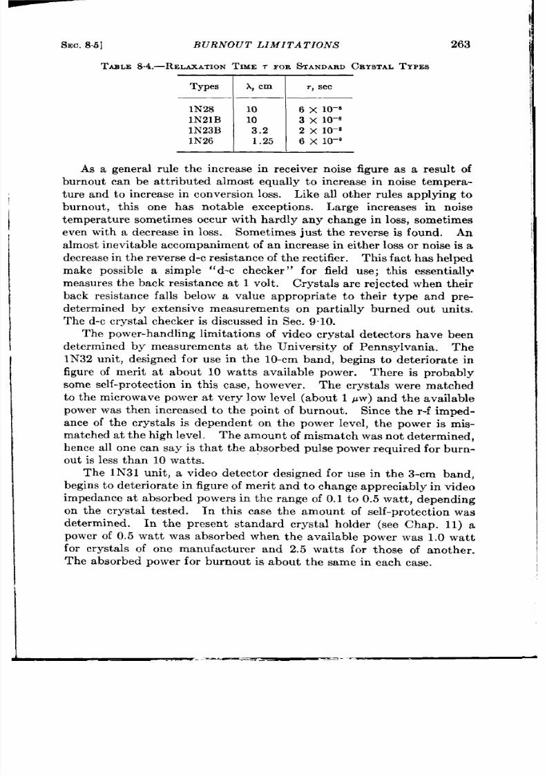
SEC.8.5]
BURNOUT LIMITATION S
263
TABLE 8.4.—RELAXATION TIME T
FOR
STANDARDCFLYSTALTYPES
1
Types
A, cm r , sec
1N28
10 6 X 10-s
1N21B 10
3 x 10-’
1N23B 3.2
2 x 10⁻⁸
1N26
1.25 6 X 10-’
As a genera l ru le the increase in receiver noise figure as a resu lt of
burnout can be at tr ibuted almost equally to increase in noise t empera-
ture and to increase in conver sion loss.
Like all other ru les applying to
burnou t , th is one has notable except ions. Large increases in noise
tempera tu re somet imes occur with hardly any change in loss, somet imes
even withade creasein loss. Somet imes just t hereverse is found. An
almost inevitable accompaniment of an increase in either loss or noise i a
decrease in the rever se d-c resistance of the rect ifier .
h is fact has helped
make possible a simple “d-c checker” for field use; this essent ially
measures the back resistance at 1 volt .
Crystals are rejected when their
back resistance falls below a value appropr ia te to their type and pre-
det ermined by e tensive measurements on par t ially bu rned ou t units.
The d-c crystal checker is discussed in S ec. 9.10.
The power-handling limita t ions of video crysta l de ector s have been
determined by measurements a t th e University of Pennsylvan ia The
1N32 unit , designed for use n the 10-cm band, begins to deter iora te in
figure of mer it a t abou t 10 wat t s available power . There is probably
some sel -protect ion in th is case, however . The crysta ls were matched
to the microwave power a t very low level (abou t 1 pw) and the available
power was then increased to the poin t of burnout . Since the r -f imped-
ance of the crysta ls is dependen t on the power level, the power is mis-
matched at the high level. The amount of mismatch was not determined,
hence all one can say is tha t the absorbed pu lse power requ ired for burn-
ou t is less than 10 wat ts.
The 1N31 un it , a video detector designed for use in the 3-cm band,
begins t o det er ior at e in figu re of mer it a nd t o ch an ge a ppreciably in video
impedance at absorbed powers in the range of 0.1 to 0.5 wat t , depending
on the crysta l t ested. In th is case the amount of self-protect ion was
determined. In the presen t standard crysta l holder (see Chap. 11) a
power of 0.5 wa t t was absorbed when the available power was 1.0 wat t
for crysta ls of on manufactu rer and 2.5 wat ts for those of another .
The absorbed power for burnou t is about the same in each case.
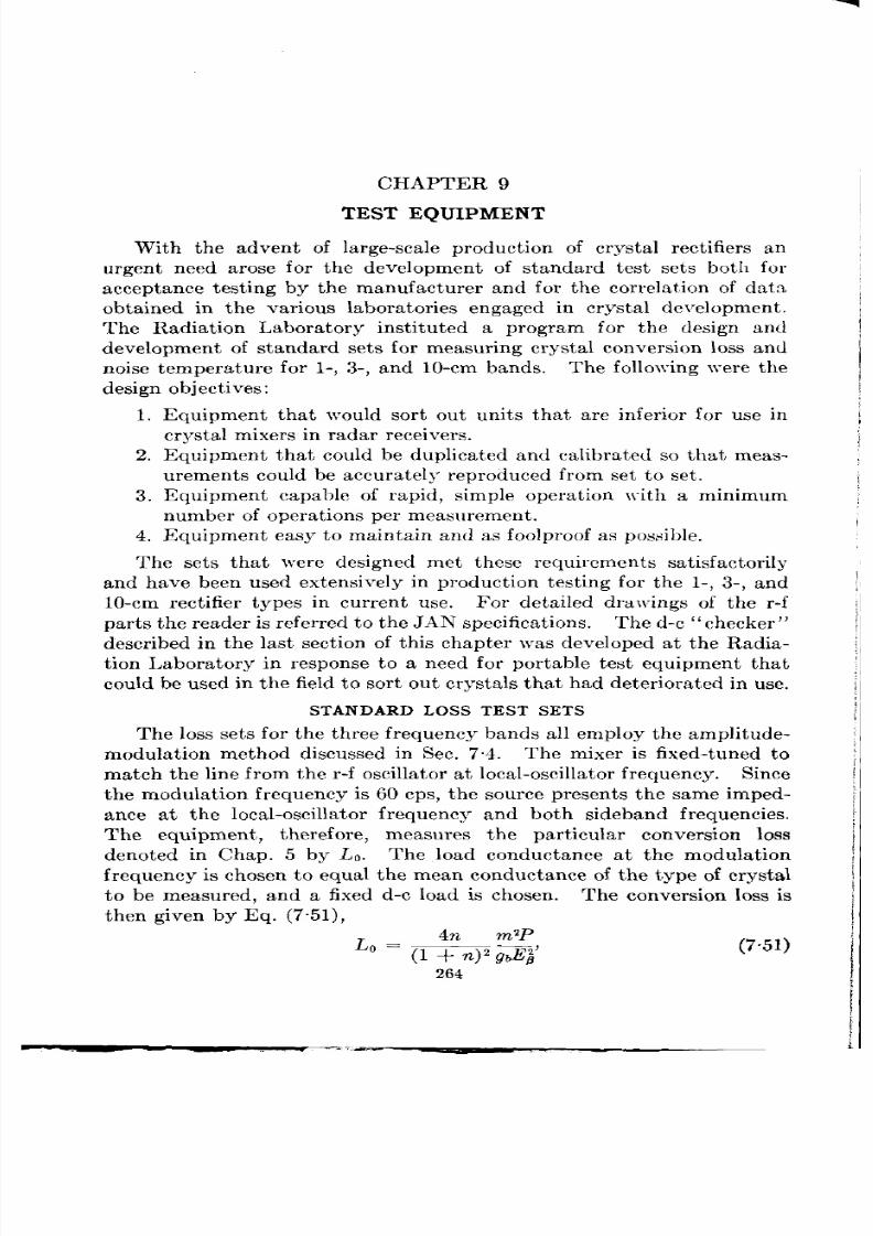
CHAPTER9
TEST EQUIPMENT
With the advent of la rge-sca le product ion o crysta l rect ifier s an
urgent need arose for the development of standard test sets both for
accept ance test ing by the manufacturer and for the cor rela t ion of da ta
obta ined in the var ious labora tor ies engaged in crysta development .
The Radia t ion Labora tory inst itu ted a program for the design and
development of standard set s for measur ing crysta l conver sion loss and
noise tempera ture for 1-, 3-, and 10-cm bands. The following v-ere the
des ign object ives:
1. Equipment that would sor t ou t units that a re infer ior for use in
crysta l mixers in radar receiver s.
2. Equipment that could be uplica ted and ca libra ted so that meas-
u rements could be accura tel~f r eproduced from set to set .
3. Equipment capable of rapid, simple oper a t ion ~vith a minimum
number of opera t ions per measurement .
4. Equipment easy to mainta in and as foolproof as possible.
The sets that wer e designed met these requ irements sa t isfactor ily
and have been used extensively in product ion test ing for the 1-, 3-, and
10-cm rect ifier types in cur ren t use.
For deta iled dr a~vings of the r -f
par ts the reader is r efer r ed to the J AN pecifica t ions. The d-c “ checker”
descr ibed in the last sect ion of this chapter was developed at the Radia -
t ion Laboratory in response to a need for por table test equ ipment that
cou ld be used in the field to sor t out crysta ls that had deter iora ted in use.
STANDARD LOSS TEST SETS
The loss sets for the thr ee frequency bands all employ the amplitude-
modula t ion method discussed in Sec. 7.4. The mixer is fixed-tuned to
match the line from the r -f oscilla tor a t local-oscilla tor fr equency.
Since
the modula t ion fr equency is 60 cps, the source presents the same imped-
ance at the local-oscilla tor frequency and both sideband frequencies.
The equipment , ther efor e, measures the par t icular conver sion loss
denoted in Chap. 5 by LO.
The load conductance at the modula t ion
frequency is chosen to e ua l the mean conductance of the type of crysta l
to be measur ed, and a fixed d-c load is chosen . The onversion loss is
then given by Eq. (7.51),
4n
~2p
‘0 = (1 + n)’ gz;’
(7.51)
264
,
I

I
I
SEC. 9.1] THE CONVERSION-LOSS SET FOR THE 3-CM BAND
265
wher e m is the modula t ion coefficient refer red t o the available power of
the oscilla tor [Eq. (7”45)], P is t he a va ila ble power fr om t he r -f o cilla tor ,
b is t he loa d con du ct an ce a t modu la tion fr equ en cy, EP is the rms modu-
lat ion volt age across the load, and n is the ra t io of the load conductance
to the i-f conductance of the par t icular crysta l being tested.
To avoid measurement of gp, the factor 4n/ (1 + n) 2 is assumed to be
unit y, Eq. (7.51) becom ing
m2p
LO=—
gbq”
(1)
It has a lready been pointed ou t that the er ror in t roduced by this approxi-
mat ion is less than 0.5 db if g6/2 < gb < 2g8; this er ror is in such a direc-
t ion as to make the unit with ext reme conductance seem worse than it
really i . Actually most crysta ls are well with in these limits; hence the
average er ror i substantial y less than 0,5 db. n any even t the approxi-
mate value is an u pper limit for conver sion loss and in acceptan ce test ing
t he appr oxim at ion t en ds t o r eject bor der lin e un its wh ose i-f con du ct an ce
differ s widely fr om t he mea n.
Similar ly the fixed tuning at radio freq ency discr iminates against
those crysta ls tha t are poor ly matched, since the available r -f power is
used for P in Eq. (l). The use of fixed tuning at both radio and inter -
media te frequencies therefore tends to select crysta ls uniform in both
r -f a nd i-f ch ar act er ist ics a nd gr ea tly simplifies t he t est pr ocedu re.
Th e
r-f tuning must be carefully standardized, however , so that mixers used
at the var ious test stat ions a re tuned accura tely alike and do not favor
t he character ist ics of th e pr oduct of some par ticular labora t ory. F or this
purpose standard r -f impedances have been developed at the Radiat ion
Laboratory; these can be inser t ed in the mixer in place of the crysta l.
The mixer is then tuned for a match at local-oscilla tor fre uency and the
tuni g adjustments sealed. The Radia t ion Laboratory served init ially
as t he standardiza t ion labora t or y, but th is funct ion has since been taken
over by the labora tor ies mainta ined by the Armed Services.
9.1. The Conversion-loss Set for the 3-cm Band.—The conversion-
10SSset for the 3-cm band, designed by Rober t s,’ was the fir st of the
standard sets to be built . z A photograph of the set is shown in Fig. 9.1,
and a block diagram in Fig. 9.2 The lower panel car r ies the r -f oscil-
la tor , cr yst al h older , a nd cir cu it s for amplit ude-modu la tin g t he oscilla tor
and for filt er ing the output of the crystal. The upper panel conta ins a
regula ted power supply for the r -f oscilla tor with a meter for measur ing
] S. Rober t s,
“Conversion Loss Measur ing Appara tus for Crysta ls in the 3-cm
Band,” RL Repor t No. 5&28, Aug. 3, 1943; a lso,
“ 1N23 Loss Measur ing Set Type
7368,” RL Repor t No. M-171, J un e 27, 1944.
e
z A limited number of se s w re manuf ctured by J . C. Fonda , Inc., 333 Four th
St ,, New York, N. Y.

266
TES T EQUIPMENT
[SEC. 9.1
the rect ified crysta l cur ren t . The voltage across the load conductance is
measured with the hIodel 300A Ballant ine voltmeter shown at the r igh t
in Fig. 9.1. In rou t ine test ing the set is ca librated with standard crysta ls
which have in turn been calibrated by the Service Laborator ies just
——- –-
.
.—
—
Lo
inches
12
——
FIG. 9.1,—The conversion-loss set for the 3-cm hand.
mentioned.
However , the equ ipment may also be used for absolu te
calibrat ion by t he incremental method, or alterna t ively, t he crysta ls may
be calibra ted with a mechanical modulator as descr ibed in Sec. 9.4.
R-j Componen ts.—The r -f componen ts are mount ed on the fron t of
the lower panel as shown in Fig. 9.3. The 723A oscilla tor is moun ted for
8
Power
supply
Modulation
circuit
8
Ballantine
voltmeter
output
circuit
F 1~, 9.2,—Block dia gr am of t he 3-cm
conversion-loss set,
conven ience in an inver t ed osit ion .
The in jector flap and ejector but ton
indicated on the photograph are de-
vices that facilit a te inser t ion and
eject ion of the crysta l in to the fair ly
st iff finger s of t h e crys ta l holder .
The
ejector is a lever ar rangement that
pushes a plunger against t he end of
t he car t ridge pin.
These devices are
an aid in rapid rout ine test ing.
A cross sect ion of the oscilla tor
mount is shown in Fig. 9.4. The
tube s cket is mounted on one side
of a sect ion of waveguide with an
adjust ing nut for varying the penet ra t ion of th e oscilla tor output antenna
through a h ole in t he waveguide.
A choke-t ype conn ect or is sold red t o
one end of the waveguide and there is a metal plug in the other end. A
resistance st r ip is inser ted parallel t o t e elect r ic field in the guide
through a slot near the closed end of the waveguide and is held by a

SEC.9.1] THE CONVERSION-LOSS SET FOR THE 3-CM BAND
267
clamp. The resist ance st r ip is adjust ed in such a way tha t the oscilla tor
mount matches the character ist ic impedance of the waveguide with the
oscilla t or a nt en na wit hdr awn .
When t he oscilla tor an tenna pen et ra t es
the wavegu ide for a small dktance, the oscilla tor is loosely coupled and
will deliver the desired 1 mw of power with only a small change in the
impedance presen ted a t the wavegu ide coupling. It can be seen tha t a
tube with low power outpu t will have to be more st rongly coupled to give
L_____---- .
nut -
“nut -
J
—
FIG. 93.-lLf compon en ts of t he 3-cm con ver biom los s set .
t he desired amoun t of power ; h en ce t he out pu t impedan ce will be a ffect ed
t o a grea t er exten t . Because the accu racy of the equipmen t depends on
holdin g close impeda nce toler ances it is clear t ha t a t ube which oscilla tes
weakly should not bc u ed.
The cryst a l holder is shown in cross sect ion in Fig. 9.5. The cry ta l
car t r idge is mounted across the waveguide and is held by spr ing con tact
fingers a t each end. The con tact a t the pin end is insu la ted and provides
a termina l for the d-c outpu t of the cryst a l; an r -f choke and bypass
condenser preven t the r -f po~vcr from leaking ou t a t th is termina l. The
cryst a l holder is in t erchangeable \ ~ith the one on the noise measu r ing
set , and for the la t t er . applica t ion the capacitance bet \ ve n the outpu t
termina l and ground should be 14 f 1 p~f.
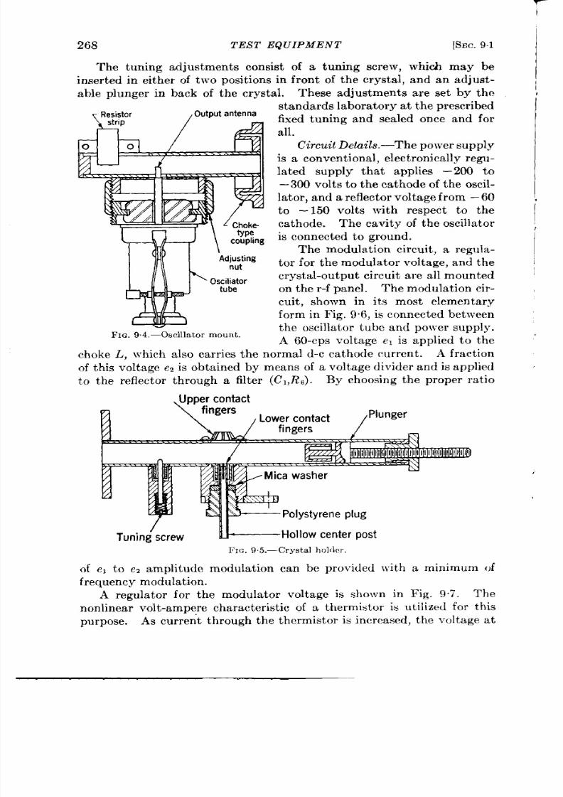
I
268
T ES T EQUIPMEN T
The tuning adjustments consist of a tuning
[SEC.9.1
screw, which may be
.
in ser ted in either of two posit ions in front of the crysta l, and an adjust-
able plunger in back of the crysta l.
These adjustments are set by the
T Resistor
, Outputantenna
FIG,
94.-Os cilla t or moun t .
st an da rds la bor at or y a t t he pr escr ibed
fixed tuning and sea led once and for
all.
Circuit Deia ils.-Th e power su pply
is a con ven tion al, elect ron ica lly r egu -
la ted supply tha t applies – 200 to
– 300 volt s to the ca thode of the oscil-
la tor , and a r eflector voltage from – 60
to – 50 volts with respect to the
ca thode. The cavity of the oscilla tor
is con nect ed t o gr ou nd.
The modula t ion circuit , a regula-
tor for the modula tor voltage, and the
cr yst al-ou tpu t cir cu it a re a ll mou nt ed
on t he r -f pa nel.
Th e modulat ion cir -
cuit , shown in its most elementary
form in Fig. 9.6, is con nect ed between
the oscilla tor tube and power supply.
A 60-cps voltage e, is applied to the
choke L, which a lso carr ies the normal d-c ca thode cur ren t . .4 fract ion
of th is voltage eJ is obta ined by means of a volt age divider and is applied
to the reflector th rough a filt er (C1,~6). By choosing the proper ra t io
Mc. 9 .5 . Crys ta l hol[lcr .
of el t o ez amplitude modu la t ion can be provided ~vith a min imum of
fr equ en cy modu la tion .
regula tor for the modu la tor volt age i shown in Fig. 97. The
non linea r volt -ampere character ist ic of a thermistor is u t ilized for this
purpose. As cur ren t t h rough the thermistor is increase , t he volt age at
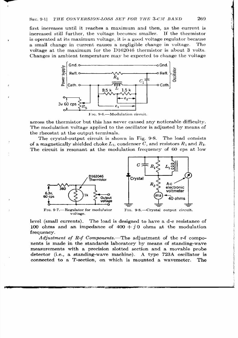
SEC. 9.1] THE CONVERS1ON-LOSS SET FOR 1’IIE 3-CM BAND
269
fir st increases unt il it reaches a maximum and then , as the current is
in cr ea sed st ill fu rt her , t he volt age becom es sma ller .
If t he t hermist or
is opera ted a t its maximum voltage, it is a good voltage regu la tor because
a small change in u rrent causes a negligible change in voltage.
The
voltage a t the maximum for the D162046 t ermistor is about 3 volt s.
Changes in ambient tempera ture may be expected to change the voltage
Grid.
E
z‘:1
~
Refl. g
~
.—
3
c1
%
0
Cath.
3V 60 CpS
J
~IG. $~6-Modulation circuit.
a cross t he th ermist or but this has n ever cau sed a ny n ot icea ble difficu lty.
The modula t ion voltage applied to the oscilla tor is adjusted by means of
the rheost t at the output terminals.
The crysta l-output ircu it is shown in Fig. 9.8. The load consists
of a magn et ica lly sh ielded ch ok e Ll, condenser C, and resistors RI and Rz.
The circuit is resonant at the modula t ion frequency of 60 cps a t low
/’w?st3r
FIG.9.7.—Regulator for modulator
voltage.
+ - +
=
FIG. 9.8.—Crystal
ou tpu t cir cu it .
level (small cu r ren t s).
The load is designed to have a d-c resistance of
100 ohms and an impedance of 400 + j O ohms at the modula t ion
frequency.
Adjustment of R-f Componen s.-The adjustment of the r -f compo-
nents is made in the standards labora tory by means of standing-wave
measurements with a precision slot ted sect ion and a movable probe
detector (i.e., a standing-wave machine). A type 723A oscilla tor is
connected to a T-sect ion , on which is mounted a wavemeter .
The
I
,

270
7’1<s7’EQ[; [l ’1wE.1-7’ [sm. 91
T-sect ion is connected to a wavegu ide at tenua tor , ~vhich is in tu rn con -
n ect ed t o t he slot ted sect ion .
The mixer or oscilla tor moun t to be tuned
is con nected direct ly to the flange coupling on th e slot t ed sect ion .
Th e
oscilla tor is tuned to th e standard frequency corresponding to 3.200 cm,
and th e tun ing devices on the r -f compon en t a rc a j u stecl for a stancfing-
wa ve r at io as n ea r u nit y a s possible.
Wit h pr ecision equ ipm en t a nd ca re-
fu l adju stm en t t he volt age sta ncfin g-~vave r at io ca n be m ade 1.01 or less,
Such accuracy is needed because small differences in the mixer tun ing
m ake appre ia ble differ en ces in values obta in ed for t he con ver sion loss of
crysta ls which a re a t th e cxt rcmcs of the impedance dist r ibut ion . ‘l’he
inside dimensions of the wavcgu idc for he slot t ed sect ion , as well as for
the oth er r -f componen t s, should bc un iform and accura te.
The standard fixed tun ing is established by tuning a standard mixer
t om at ch t ot hech ar act er ist ic a {lm it ta nccof t he~va vegu icle cr yst als \ r it h
an r-f impedance a t the cen ter of the impedance dist r ibut ion .
Once
-Ceramic
~Solder~
Adjustlngd -
screw
FIG. 9.9.—St an da rd-im peda nce ca rt ridge for t he 3-cn l ba nd,
such a standard mixer is established, a standard-impedance ca r t r idge
that ma tches in the standard mixer is used f r tuning other mixers.
The standard-impedance ca r t r idge used for the 3-cm band is sho~rn
in Fig. 9.9. It consist s of a thermistor moun t d ina Sylvan ia Company
ceramic ca rt r i ge and is const ru cted in the follo\ ving way.
One of the
leads of an unmounted thermistor bead (Western Elect r ic D- 63903) is
soldered to the screw tha t normally ca r r ies the ilicon crysta l.
Th e
screw is then inser ted in the ca r t r idge and the pin end of the ca r t r idge
hea ted with the resu lt tha t , as the screw is advanced, th e wire on the
other end of the thermistor bead dips in to the molten solder inside the
ca r t r idge on the pin end.
The screw is advanced un til the bead is
cen tered in the hole in the ceramic. The desired impedance is obta ined
by adjust ing the amount of solder a t the two ends of the ca r t r idge and by
adjust ing the resistance of the thermistor .
Th e esista nce is a dju sted
by connect ing the ca r t r idge in one arm of a br idge and adjust ing the
br idge cu r r en t .
On ce t he desir ed combin at ion of t hese va ria bles k fou nd,
a specifica tion of th e resista nce determ in es un iqu ely t he im pedan ce of th e
ca r t r idge. The d-c resistance requ ired to match th e var ious ca r t r i ges to
the sta dard 3-cm mixer is in the range of 30 to 50 ohms. The impedance
SEC. 91]
THE CON VERS ION-LOSS SET FOR THE 3-CM BAND
271
va r ies slight ly with the or ien ta t ion of the car t r idge in the mixer ; t her e-
for e both the or ien ta t ion and resistance must be specified. The 3-cm
impedance standard has an admit tance in the waveguide, when refer r ed
to the plane of the car t r idge, of about 1.25 + ~ 0.5 t imes the char acter -
ist ic admit tance of the wavegu ide.
It should be emphasized tha t the pr imary standard is t he standard
mixer . The essent ia l funct ion of the standard impedance is to provide a
simple means of tun ng other mixers so as to be ident ica l with the stand-
a rd. The use of a stable impedance standard, moreover , provides a
means of checking the constancy of the mixer -impedance combina t ion .
The impedance standard is a lso equa lly usefu l as a bolometer for the
measur ements of r -f power requ ired for the absolute measu ement of
con ver sion loss.
Adjustm ent and Calibration of the A’et.-A wavemeter , mounted on a
T-sect ion , is inser ted between the oscilla tor mount and the mixer for
a dju st in g t he fr equ en cy of t he osc lla tor t o t he st an da rd va lu e cor respon d-
ing to 3.200 cm. The equipment is sufficien t ly stable to requ ir e only an
occa siona l check on fr equency.
Calibra t i n of th e equipment is a ccom-
plished with seconda ry-st andard crysta ls provided by the standard:
la bor at or y, for wh ich t he con ver sion loss a nd r ect ified cu rr en t a re kn own .
The power -level adjustment is ade by means o the large adjust ing nut
on the oscilla tor mount , and is locked by means of the small locking llLlt
(see Fig. 93). This adjustment cont rols the distance tha t the outpu t
an tenna penet r a t es in to the waveguide, thereby varying the coupling of
t he oscilla tor t o t he wa vegu ide.
The power level is so adjusted tha t the
value of the rect ified cur ren t for a given crysta l is tha t in the specifica-
t ions, 1 mw of ava ilable power being obta ined by th is adju tment .
From Eq. (I) it is seen tha t the conver sion loss of the crysta l, in
decibels, is given by
( )
2P
L(db) =
10 logl, —
– 20 Ioglci
EP.
gb
#
(2)
The decibel sca le on the Ballan t ine voltmeter gives 20 log10
E ; d irectly.
1
The ot er constan ts in Eq. (2) are known, except for m, which is difficult
t o measure for the modula t ion method used in the equipment . Accord-
in gly, t he con ver sion loss of t he st an da r cr yst als a re u sed for ca libr at ion .
Th e voltmet er is set on t he O.01-volt fu ll-sca le r an ge, a nd t he modu la tion
volt age adjust ed so tha t the t erm 10 loglo (m2P/gb) is equal to 20.0. For
th is set t ing the output -voltmeter reading on the decibel sca le is 20.o
inus the value of conver sion loss specified for the standard crysta l.
This cor responds to a va lue m of of 1.58 per cen t for P = 1 mw and
g&,= & rnho. The conversion loss of an unknown crysta l in decibels is
then just 20.0 minus the reading of the output meter in decibels.
272
TEST EQUIPMENT
[SEC. 92
It i desirable to use a set of severa l st anda rd crysta ls for the ca libra-
t ion in order t o detect any deter iora t ion of an individual unit th rough
handling. To avoid damaging crysta ls the equipment shou ld be con-
nect ed to a good ground. The opera t or should place his hand on the
equipment just pr ior t o inser t ing the cryst a l car t r idge and while he is
inser t ing it in order to avoid burning out the crysta l by the discharge of
sta t ic elect r icit y tha t may have accumula t ed on his body.
The Ca ibration oj S tandard Crysta ls.—The st anda rd c ysta ls can be
ca libra t ed by the incrementa l method or by the amplitude-modula t ion
method. Both of these methods a re discussed in Sec. 7.4. Th e la t ter
meth od ut ilizes a mech anica l modula tor for which t he modula t ion coeffi-
cien t can be accura t ely measu red; th is is discussed in deta il in Sec. 9.4.
For the incremen ta l method, it was shown in Sec. 7.4 tha t the conversion
loss is given by
L= ‘b ,,
()
2P, ~+
(3)
wh er e gL,s t he st an da rd loa d con du ct an ce a nd AZ is t he in cr em en t of r ect i-
fied cu rr en t in t he loa d r esist an ce rz of F ig. 7.7b when t he a va ila ble power
is in cr ea sed fr om P t o P + AP. The quan t ity Po is the average power ,
P + ~ AP. These quant it ies can all be measu red on the conver sion -loss
set . For the power measuremen s a micrometer a t t enua tor , such as is
used on the noise set (see Fig. 9.24), is in ser t ed between the oscilla tor
moun t and the crysta l holder . The a t t enua tor can be ca libra ted by
using the stand rd-i pedance ca r t r idge as a bolometer in one arm of a
br idge. The easu remen t of the cu r ren t increme t AI is accomplished
with the circu it of Fig. 7.7b. The r-f panel of the loss set is provided
with a switch tha t connect s the ou tpu t t ermina l of the mixer either
t o the usual load circu it or to a t ermina l to which the ca libra t ing circu it
of F ig. 7.7b is connected. In making the measurement at t he standard
power level of 1 mw the ca libra ted at tenuator is first set for 0.9 mw
available power and the cur ren t th rough the outpu t meter is ba lanced
out . The a t tenua tor i t hen sh i ted to the 1. l-r ow level and the cu r ren t
AI th rough the meter noted.
For a load resist ance of 400 ohms the
con ver sion loss is given by
(4)
where A is 20/ma2 wh en AI is expr essed in millia mperes. With pr ecision
equipment , an accu racy of 0.1 db can be obta ined. For th is accu racy
an a t t enua tor tha t ma tches the wavegu ide accu ra tely must be used.
9.2. Th e Con version-loss Set for t he 10-cm Ba nd.-Th e developm ent
of the conver sion -loss set for the lo-cm band followed chronologica l y

SEC.
9,2] THl?
CONVIIRS IO.V- OSS SET FOR T IIE 1O-C’M BAND
273
that for the 3-cm band and is similar t o it in many respects; t he differences
are ch iefly in the r -f components.
A photograph of the set , developed
)
at the Radiat ion Laboratory bj- Hunt ington , 1 is shown in Fig. 9.10, and
a block diagram in Fig. 9.11.
The top panel contains the po~ver supply
for the type 707B oscilla tor ; t he middle panel contains the modulat ion
circuit and the crysta l-ou tput circuit ; the bot tom panel suppor t s t he r -f
*
I
.
FIG. 9 .10.—The convers ion-loss set for the 10-cm band.
oscilla tor , a t t enuator , and mixer .
‘l’he output modulat ion volt age is
measured, as in the 3-cm set , with a Ballant ine voltmeter .
R-f Component s.—The r-f oscilla tor and mixer a re moun ted on the
back of the panel, as shown in Fig. 9.12. The oscilla tor is moun ted in a
broadband cavity, designed for a sh ielded wideband signal genera tor ;
it is u sed here because of it s stu rdy const ruct ion and the ease with which
it is moun ted and tuned. The ca~-ity has two tuning plunger s, one for
gross and the other for fine adjustment . The tuning knob for the la t t er
I H. B. H un tin gt on , “ 1X21 Loss Test er Type 7556, ” RL Report No. LI-177, Au g.
I
21, 1944. The set was manufactured in limited quant it ies by Photoswitcb, Inc., 77
Broadway, Cambr idge, Mass.
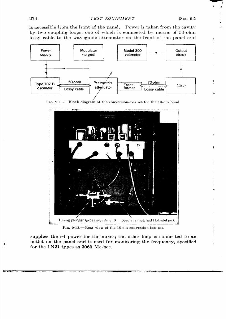
274
TEST EQUIPME,YT [SEC.92
is accessible from the f ren t of the panel.
Power is t ken fr m the cavity
by two coupling loops, one of wh ich is connect ed by means of 50-ohm
lossy cable to the wavegu idc at tenuator on the fron t of the panel ancl
~,,
Power
Modulator
Model 300
supply
output
(to grid)
voltmeter circuit
1 (
Type 707 B
50.ohm
Waveg;ide
+ )
F
Trans.
70.ohm
attenuator
h
r.;}xer
oscil!.ator
Lossycable
former
Lossy cable
/
I :lG. 9. I l.—Block d iagram of the conver s ion -los s set for the 10-cm ba ,,d .
r-’-
I
[ Tuning plu’nger(grossad)ust,nent,
Specl; lly matched Holmdel lack
FIG. 9 .12.—Resu view of the lo-cm conver sion -los s s et .
supplies the r -f power for the mixer ; t he other loop is connected to an
ou t let on the panel and is used for mon itor ing t e frequency, specified
for t he 1N21 t ypes as 3060 ilfc/sec.
I
.
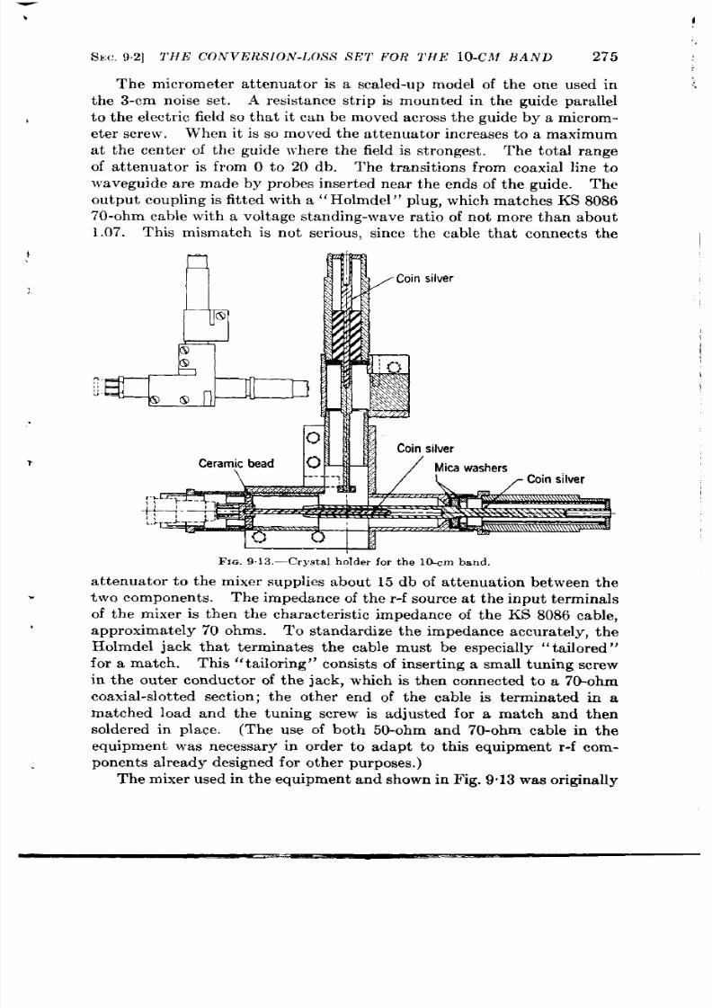
,
SEC. 92] THE CONVERS ION-LOS S SET FOR THE IO-CM BAND 275
The micrometer a t tenuator is a sca led-up model of the one used in
the 3-cm noise set .
A resistance str ip is mounted in the guide para llel
to the elect r ic field so that it can be moved across the guide by a microm-
eter screw. W en it is so moved the a t tenua tor increases to a maximum
at the cen ter of the guide \ vhere the field is strongest .
The tota l range
of a t tenua or is from O to 20 db. The transit ions from coaxia l line to
waveguide a re made by probes inser ted near the ends of th guide. The
output coupling is fit ted with a “ Holmdel” plug, which matches KS 8086
70-ohm cable with a voltage standing-wave ra t io of not more than about
1.07. This mismatch is not serious, since the cable tha t connects the
r--i
\
.
FIG. 9 .13.—Crys ta l holder for the lCLcm band.
a t tenuator to the mixer supplies about 15 db of at tenuat ion between the
two components. The impedance of the r -f source a t the input terminals
of the mixer is then the character ist ic impedance of the KS 8086 cable,
approximately 70 ohms. To standardize the impedance accura tely, the
Holmdel jack tha t terminates the cable must be especia lly “ ta ilored”
or a match . This “ta ilor ing” consists of insert ing a small tuning screw
in the ou ter conductor of the jack, w ich is then connected to a 70-ohrn
coaxia l-slot ted sect ion; the other end of the cable is terminated in a
matched load and the tuning screw is adjusted for a match and then
soldered in place. (The use of both 50-ohm and 70-ohm cable in the
equipment was necessary in order to adapt to this equipment r -f com-
pon en ts a lr ea dy design ed for ot her pu rposes.)
Th e mixer u sed in t he equ ipmen t and sh own in F ig. 9c13 wa s origin ally

276
TES T EQUIPMEN T
[SEC. 9$
design ed by Sh ar plessl a t t he Bell Teleph on e La bor at or ies i or con ver sion -
10SSmeasurement s by the hetero yne met od. It was adapted t o the
amplit ude-modu la tion m et hod by r emovin g t he Holmdel plu g t ha t ca rr ies
the capacity coupling for the loca l oscilla tor . A brass plug closes the
hole th rough which th is coupling was made.
The crysta l t ermina tes one end of a coaxia l line, t he other end being
connected t o the i-f ou tpu t plug.
A quar ter -wave choke in th is plug
and a bypass condenser preven t the r -f power from leaking ou t a t th is
termina l. The capacity seen looklng in to the i-f termina ls is adjust ed to
the specified value of 15 ppf by adding or removing mica washers in the
bypass condenser . The r -f input ine is connected t o the crysta l by a
capacity coupling. The two tun ing adjustment s a re the capacitance
of th is coupling nd th length of line between the cryst a l and the r -f
shor t cir cu it in the i-f plug. The cryst a l is held in the crysta l r eceptacle
by spr ing fingers on the inner and out er onductors of the coaxial line.
Circu it Deta ils.—The circu it deta ils a re similar in every respect to
those for the 3-cm set except that t he 60-cps amplit ude-modu la t ion
voltage is applied to the gr id of the type 707B tube. The modulat ion
voltage is regu la t ed by the thermistor circu it of F ig. 9.7. The outpu t
circuit is t he same as tha in Fig. 9.8; t he load impedance at 60 cps is
400 + j O ohms.
Adjustment
of
R -f
Components.—The mixer is tuned by means of a
standing-wave machine fit ted wit h a 70-ohm Holmde! jack , in to which
the mixer is plugged. The s andard impedance is a thermistor ca r t r idge
wh ich differ s fr om t ha t sh own in F ig. 9.9 in t he followin g r espect s.
(1) .4
th i~ ~ylindr ica l met al sleeve, 0.180 in . long, is placed a roun d t he cer amic
on the pin end of the ca r t r idge; th is sleeve is flush with the end of the
c ramic on the pin end and is soldered to the brass fit t ing on tha t end.
(2) Solder is add d to the connect ions inside the ca r t r idge unt il t h ere is
barely enough spa e for the thermistor bead between the two balls of
solder tha t a re formed. (3) With the above var iables proper ly adjust ed,
t he desir ed im peda nce is obt ain ed for t hermist or r esist an ces va ryin g fr om
100 to 110 ohms.
Calitn-a t ion of the Set .—The calibra t ion of the set is the same as tha t
descr ibed in Sec. 9“1. The sp cified ava ilable power is 0.5 mw, and the
load resistance a t 60 cps is 400 ohms. The constan t A in Eq. (4) is
ther efore 10.0/ma2 when AP is 0.2 mw.
9.3. The Conver sion -loss Set for the l-cm Band.—The conver sion -
10SSset for the l-cm band was developed a t the Radia t ion Labora tory’
1W. >1. Sharpless,
‘ ‘Lfanufa ct u rin g E lect r ica l Tes tin g Requ ir emen t s—lN21
Cr yst al Rect ifier ,” BTL Repor t llilI-43-160-167, Ot t. 14, 1943.
z C. A. Wh itmer , “A Conver sion -Los s Set for Test in g K-ba nd Cr yst al Rect ifier s,”
RL Repor t No. 668, J an . 16, 1945.

SEC. 9.3] THE CONVERS ION-LOS S SET FOR THE l-CM BAND
277
toward the end of the crysta l-development work and did not go in to
product ion . A block diagram of the set is shown in F ig. 9“14. A
mechanica l modula tor produces the amplitude modula t ion , and the out -
put circu it is designed for measur ing both the i-f resistance and the
conversion loss. The set opera tes at the specified test wavelength of
1.250 cm, and the r -f components, except the modula tor and crysta l
holder , a re standard test equipment , descr ibed in deta il in Vol. 11 of the
Ra dia tion La bor at or y Ser ies.
R -j Compon en ts.—A
type 2K33 oscilla tor , or its equiva lent , with a
minimum r-f power output of 20 mw is required for the equipment .
This provides 1 mw of available power to the crysta l and at the same t ime
makes possible the use of a t least 6 db of a t tenuat ion on each side of the
mechanica l modula tor . The r-f admit tance of the modu la tor differs
modula tor ; for cer ta in or ien ta t ions of th e modula tor disk, th e modula tor
may be mismatched to the waveguide by as much as 1.1 in voltage
h t
t I I I
‘-/
Power
supply
l-=J-@J
t
[
I
2K.33
Crystal
oscdlator holder
I
FIG, 9.14.—Block diagram of the conversion-loss set for t he l-cm band.
st an din g-wa ve r at io (see Sec. 9.4).
The at tenuat ion between the modu
la tor and oscilla tor is used so that this var ia t ion in load impedance will not
modula te the oscilla tor output by an unpredicted amount .
Similarly,
there should be ample a t tenua t ion between the oscilla tor and mixer so
tha t the character ist ic admit tance of the waveg ide is a lways presented
to the mixer .
The a t tenuators a re “vane” at tenuators, var ied by varying the pro-
j ect ion of a resistance str ip through a slot in to the wavegu ide para llel
t o t he elect ric field.
The mechanica l modula tor is similar to tha t descr ibed in Sec. 9.4
for the 3-cm waveguide. The at tenuat ing disk, 1 n . in diameter , is
rot a ted by a small motor mounted r igidly to the waveguide.
The
eccent r icity of the disk is set to give a modula t ion coefficien t of about
10 per cent . This va lue gives a convenien t r ange on the output meter
with the specified r -f power and 1oad resist an te.
The motor is run at a speed of about 55 rps. Synchronous speed is t o
be a voided so as t o pr even t a fixed-ph ase rela tion bet ween t he modu la tion
voltage produced by the mechanica l modula tor and tha t produced by
any r ipple that ma be presen t in the power supply. The la t ter should,

278
TES T EQUIPMEN T
[SEC. i )~
of course, be reduced to a minimum to avoid fluctuat ions in the output
voltage. St ray magnetic fields from the motor may produce an undesir-
ab e 60-CPS modulat ion of the type 2K33 oscilla tor , but its effect can be
minimized by shielding the motor with sheet iron . By means of a stop,
the modula tor disk may be quickly set in a rest posit ion at which the same
rect ified curren t is bta ined as ith the modula tor running.
~n’ngTrewJcV’ta~~~~~u”~e’
Insulating washer and
bypass condenser
olystyrene plug
F IG. 9,15.—Crys td hold e for t h e l-cm t est equ ipmen t .
The waveguide crysta l holder is shown in cross sect ion in Fig. 9.15.
The ou ter conductor of the coaxial c r t r idge is set against the shoulder
in the crysta l receptacle; the inner conductor is held by spr ing fingers
on the end of the post that couples the crysta l to the waveguide. This
post is insulated and provides a terminal for the d-c output of the mixer .
60 Cps
~Lc;. 91[;.-0utr,ut cimu; t.
An r-f choke and bypass con enser prevent leakage of r -f po~~er at this
terminal. The tuning adjustment consist s of a tuning scre\ v in f rent
of the crysta l and an adjustable choke plunger behind the crystal. A
spring device, not shown in Fig. 9.15, is u sed for sea t ing the car t r idge
Crmly in the crysta l receptacle.
Circu it Deta il; .—The ou tpu t circu it is shown in Fig. ‘+16. It pro-
vides the specified d-c load of 100 ohms and a-c load of 500 ohms, and a lso
~
J
)
(
I
SW. 9.31 THE CON VERS ION-LOSS SET FOR THE l-CM BAND 279
provides for th e measurement of crysta l resistance a t 60 CPS. The circuit
is opera t ed in the following way.
The switches SI and Sz re ganged in
such a way tha t S2 is closed when S 1 is open.
With Sz closed, the
potent iometer RI is adjusted for zero current in the galvanometers G.
Under this condit ion , cur ren t from the power supply balances out the
rect ified cur rent from the crysta l in G; the d-c load is then 100 ohms and
the a-c load 500 ohms. The rect ified current is read on the milliammet r
and the a-c volt age is read by c1osing witch S to posit ion 2.
The circuit provides a variable 60-cps voltage tha t may be conn ected
to the crysta l in ser ies with a resistance of 100,000 ohms by closing
switch S,. Since the i-f resistance of the crysta l is in the range from
300 to 600 ohms, essent ia lly a con stant -cu rrent sou rce is thus provided.
The i-f resistance can then be determined by reading the voltage across
the crysta with the output meter .
With some 2K33 tubes the 60-cps
heater supply will produce a 60-CPS modula t ion in the r -f power , which
will then in t roduce an er ror in the resistance measurement . This situa-
supply.
Either the Ballan t ine model 300 voltmeter or the Hewlet t -Packard
model 400A voltmeter may be used for measu ing the output voltage.
The former has a logarithmic meter that can be read more accura tely
than the Hewlet t-Packard in the range needed under actua l opera t ing
condit ions and is therefore prefer red for absolu te ca libra t ion . The
Hewlet t-Packard meter is perhaps to be prefer red once the equipment is
ca libra ted and standard crysta ls are available. The gain of the meter
can be changed in such a way that the indica t ion is in the most sensit ive
par t of the scale for crysta ls in the acceptable range. A variable gain
con t rol makes it possible to set the meter for direct reading of the con-
version loss.
Adjustment
of R -f
Compon en ts.—Th e adjustmen t of t he mecha nica l
modu la tor is descr ibed in Sec. 9.4.
The standard mixer is tuned to match the wavegui e when a 65-o m
terminat ion is plugged in to th e crysta l receptacle. The 65-ohm termina-
t ion for tuning the standard mixer is a coaxial line terminated by a
resistance cloth wound around the cen ter condu ctor in the form of a cone.
If th e con e is shaped so as to terminate th e line in its character ist ic imped-
ance, then , for an arbit ra ry tuning of the mixer , a change in the posit ion
of the cone along the line will not shift the posit ion of the minimum of the
standing wave in the slot ted sect ion .
Once this condi ion is achieved
t he sta ndar d m ixer ca n be fixed-tu ned for a st an din g-~}-a ve r at io of un it y.
The terminat ion just descr ibed is not stable enough for a standard
impedance. The st andard impedance used for tun ing mixers to match
the st andard one is shown in Fig. 9“ 17.
It consist s of a shor t sect ion of

280
TES T EQUIPMEN T
[SEC.9.4
coa xia l lin e of 65-ohm ch ara cter ist ic impeda nce; on e en d of it is iden tica l
with the pin end of the car t r idge for the l-cm band, the other end is
short -circu ited. The ou ter conductor is slot ted longitudinal y and rec-
tangular st r ips of resistance card are inser ted on each side so that they
make con ta ct wit h t he in ner condu c-
tor . This device can be matched
to the standard mixer by sliding
M,, the st r ips along the slots. Once the
a ‘:::;:h :’::’::
st r ips are clamped in the slots and
surface. Such a terminat ion has
the requ ired stability and rugged-
FIG.
9 ,17.—Standard 65-ohm termina t ion .
ness, and the adjustmen t procedu re
ensures its having the r equired impedance.
The procedu re for fixing the tun ing of mixers is simila r t o tha t
descr ibed for the other bands.
a l&at~On of the ~et .—The mechanica l modu la or is ca librated by the
method descr ibed in Sec. 9.4. Once m is known , the constan t t erm in
Eq. (2) can be ca lcu la ted. To measu re the ava ilable power 1’0, t he mixer
is replaced by a matched Wollaston wire or thermistor bolometer .
Once
a set of standard crysta ls is ava ilable, it may be used for checking the
ca librat ion of the equi men t as descr ibed in Sec. 9.1.
If t he set is u sed for the measurement of conversion loss on ly, t he
modu la tor may be run cont inuously.
The measu rement then involves
set tin g t he pot en tiom et er RI (F ig. 9.16) for a null reading of the galva-
n omet er s a nd r ea din g t he ou t pu t voltmet er .
To measure the i-f resistance, th e modulator is stopped at the fiducial
posit ion and S1 is closed. The output voltmeter is then read with s
closed first to posit ion 1, then to posit ion 2.
For readings V, and Vz,
the i-f resistance is given by
(5)
With VI fixed at a su itable va lue, t he resist ance is obt a ined from a single
reading of the ou tpu t meter .
9.4. The Mechan ical Modula tor .—The use of the mechanica l modu-
la tor for absolu te conversion-loss measurement s has a lready been men-
t ioned in Sec. 7.4.
The modula tor developed by Rober t sl for t he 3-cm
band is shown in the photograph of Fig. 9.18. It is essen t ia lly a var iable
a t tenua tor dr iven by a motor , t he a t tenua t ion c onse(luen t l y varying
1 S. Rober ts, “ .L N lech an ica l h fodu ]:,t or : n d
I’rccisc .
IcLIIod Of calibration for
Crys ta l Conver sion Loss St a ndar diza t ion , ”
I{L Gr ou p Repor t 53, J an , 5, 1945.
/
I
I
I
I
SEC.
9.4]
T IIE MECHAN ICAL MODULATOR 281
per iodica lly a t a frequency slight ly less than 60 cps. The a t t enua tor
consist s of a th in insula t ing circu lar disk, 2+ in . in diameter , wh ich has a
u iform resistance coa t ing on one surface and penet ra t es a slot on the
top side of a sect ion of wavegu ide.
The disk in t roduces more or less
a t tenua t ion depending on how far it penet ra t es the wavegu ide.
It is
moun ted eccen t r ca lly on the shaft of the motor , the a t tenua t ion there-
fore va rying per iodica lly as the sha f rota t es. The mount ing hole in
the disk is eccen t r ic with respect t o the ou ter edge, and the bush ing
on which it is moun ted is a lso eccen t r ic. As a resu lt , t he eccen t r icity
of the ou ter edge of the disk with respect to the motor sha ft can be
adjusted smooth ly by rota t ing the disk on the mount ing bush ing. By
th is means the modula t ion coefficien t of th e modula tor can be set a t the
Li — ...
— -—
I’1~. 91S.-Mcchanica l mc ula tor for the
3-cm equipment ,
Resistance. coated disk
r
Set screw (2)
I
S et screw (3)
FIG. 9.19.—Mounting bushing for
t he modula tor disk.
desir ed value. The const ruct ion o the bushing and resistor disk is
showm in Fig. 9“19.
The average penet r a t ion of the disk inside the wa eguide is ra ther
cr it ical. If it penet r a tes too far , t he waveform of the modulat ion tends,
because of ir regular it ies in the resistance coat ing, to be nonsinusoida l.
On the other hand, if t he penet r a t ion is so adjusted that the waveform
is near ly sinusoida l, the r -f impedance is affected-tha t is, the impedance
seen on looking in to one side of the modula tor with a matched termina-
t ion on the other side is not the character ist ic impedance of the wave-
gu ide. Fur thermore, as has been poin t ed ou t in Sec. 9.3, th is impedance
var ies with the rot at ion of the modu la tor . It is preferable to adjust the
penet r a t ion in such a way that the modu la t ion is as near ly sinusoida l as
possible and to compensa te for the impedance mismatch by the use of
a t tenuators on each side of the modu la tor . F igu re 9.20 shows the
var ia t ion in power t ransmission as a funct ion of angle for a typical

282
T ES T EQUIPMEN T
[SEC.
94
modula tor . F igure 9.21 shows the standing-wave ra t io as a funct ion of
angle.
With con st an t in ciden t power t he power t ra nsm it t ed by t he modu la tor
is a per iodic funct ion of the angular posit ion 6 and may be represen ted
by t he F our ier ser ies,
P= PJ l+a~cos (f3+f#m)+a2cos(20+ 42)+”” -+1,
(6)
where PI is the average power and ai and & are constants.
Th e modu-
0.20,.
z
z
-
E
z
g
0.1635
.
s
~ 0.15
/
o
90 1s0 270
360
Onentatlonof modulatord!sk in degrees
o
90
F IG. 9.20.—Tr an sm iss ion ch a ra ct er ist ic of a mech an ica l modula tor .
.$ 1.15
-
:
3 1.10
0
0
y
<
0
p
g 1.05
--z
i%
s
3 1.00
0 90
I&o
270 360
Orientation of modulator disk in degrees 0
90
F IG. 9.21 .—St an din g-wa ve r at io of mech a nica l modu la t or .
la er is adjusted to minimize a ,, a ,, et c., the resultan t power , to a good q
a ppr oxim at ion , bein g given t her efor e by
P = P,(I + 2m cos 0),
(7)
where the modula t ion coefficien t m = ~a 1.
The value of m may be determined by a Four ier analysis of the t rans-
mission character ist ic given in Fig. 9.20. Instead of in tegra t ing to find
the coefficien ts of the fundamenta l-frequency c mponents, accura te
result s can be obta ined by summat ions with fin ite in terva ls of 30°.
Expressed in terms of summat ions over equally spaced values of O in the
SEC, 95] THE .VOIS E MEASURIVG SET FOR T E 2-CM BAND
283
r an ge fr om 0° t o 360°, t he modula t ion coefficien t is
~ = ~(ZP cos 0)’ + (ZI’sin 0)2
2P
(8)
The modu la t ion coefficien t ca lcu lat ed from the cu rve of Fig. 9.20 by
means of Eq. (8) is 0.100.
STANDARD NOISE TEST SETS
Standard noise set s were developed at t he Radiat ion Laboratory f r
the 3-cm and 10-cm bands. Accept ance tes ing in the l-cm band is
o Inches
12
-.
ICI(;. 922. -TI1c sta ndiwd n oise-m r:lsu rin g set for t he 3-cm h
IL
done at presen t }vit ,h the s-cm noise set , using an aclaptcr on the 3-cm
crystal holder \ vh ich makes it possible to plug the l-cm coaxia l car t r idge
in to the holder . Both of the standarcl set s employ the Rober t s coupling
circu it descr ibed in Sec. 7.6; in both , the noise tempera tu re is measured
by compar ing the noise power ou tpu t of t he crysta l ]vith that of a stand-
a rd r esist or .
9.6. The Noise Measu r ing Set for the 3-cm Band.—The set for
measur ing noise t empera tu re in the 3-cm band J VaSdeveloped by Rob-
284 T ES T EQUIPMEN T
er t s. 1
A photograph of the equ ipment is shown
1
[SEC.95
in Fig. 9.22, and a block
diagram in Fig. 9.23. The bot tom anel includes the r -f componen t s,
input coupling circu it , diode noise source, a d preamplifier . The second 1
pa nel ca rr ies a r egu la ted power su pply for t he pr eamplifier , a nd a n ou tpu t
9F
1
1
Type 723 A/B Halllcrafter
Coupling
Preamphfler
oscillator
S.36 recewe~
circuit and
noisediode
1f
I
Vane
1:
R.f filter
Micrometer
crystal
I
attenuator
attenuator
holder
FIG. 923.-Block diagramof th e noise-measuringet for the 3-cm band
..
Vane type
~ ‘:~~n~r attenuator
Micrometer
Injector
attenuator ~~d~~
/ Filter I
fpp
I
1
~ \ clamp\ --nut” 0
Clamp
~!ut Oscillator
Adjusting
nut
I
.
.-. .
.
—d
IJIG.924.-IL-1 panelof th e 3-r]n noiseset.
meter and louds~cakcr for the Hallicraftcr S-36 receiver .
The th ird
panel is a power ~uppl y for the r -f oscilla tor ; on th is panel a re mounted
meters for measur ing the re~i,iiicd crystal cur ren t and the beam curren t
of the oscilla tor . The top panel is a Hallicraftcr S- 6 receiver . A type
VR-307 volt age regula or mounted on the bot tom of the cabinet in the
1 S, Rober ts, “ 1N23 Noise Nfca su i-in g Set , ‘r ypc 7438,” RI, Report No. NI-190,
I)ec, 21, 1944. ‘r his set wa s m an ufa ct ur ed in lim it ed qu an tit ies by J . C, F on da , In c.,
New York, N. Y.
\
I
\
I
I
I
I
I
\
SEC.
95]
THE NOISE MEASURING SET FOR THE 3-CM BAND
285
rea r pr ovides stabilized a-c volta ge for th e r eceiver , preamplifier power
su pply, a nd t he oscilla tor ca th ode h ea ter .
R-f Components.—A ph otogra ph of t he r -f panel is sh own in Fig. 9“24.
conver sion loss set .
A descr ipt ion of the micrometer
a t tenua tor was given in Sec. 9 2. The
en ds of t he r esist an ce st rip in t he at ten-
ua tor a re taper ed; hence the cha rac-
ter ist ic waveguide impedance is seen
on looking in at either end. The
purpose of this a t t enua tor is to pr e-
sent the character ist ic impedance of
the wavegu ide to the crysta l holder a t
signa l and image fr e uencies as well as
a t l ca l-oscilla tor fr equency; it is
of 5-db
attenuation.
The vane-type a t tenua tor oper -
a tes by moving a resistance-coa ted
card into the waveguide (p r a llel to
F Ici. 9.25.—R-f filt er .
~he elect ic field) through a slot
in the top of the guide. This a t t enuator is su itable for varying the
a t te ua t ion rapidly when a ca libra t ion is not required.
It is not used
in the standard procedure for 3-cm test ing but is usefu l in t est ing 1N26
rect ifiers, where the r -f power level is adjusted for a minimum rect ified
cu rren t of 0.5 ma.
The r-f filt er shown in cross sect ion in Fig. 9.25 is a wavegu ide res-
on at or wit h ir is cou plin g a nd a ch ok e-t ype
tuning screw. The Q of th is filt er is about
‘#&}~ screvisthensea led. Thepuposeofhe
- (X-6030) 1000, and its t ransmission loss somewha t
less than 2 db. It is tuned to the standard
test frequen y of 9375 Me/see, the tuning
2 45-v
ban.
fuse
filter is to reject
t he noise sideba nds
FIG. 926.-Diode P ower SUPPIY.
genera t ed by the oscilla tor . Without it ,
the indica ted noise t empera tur e is appreciably h igher than the t rue noise
tempera ture of the crysta l.
Circuit Deta ils.—The oscilla tor power supply is ident ica l with tha t
used in the 3-cm conver sion loss set . The preamplifier power supply
provides a r egu la ted volt age of 105 volt s for the preamplifier . A con -
ven ien t power supply for the noise diode (not included in the equipment )
is sho~vn in ig. 9.26. It is completely sh ielded.
The input coupling circu it is t he Rober ts cir cu it discussed in Sec. 7.6.

286
1’ESI’ EQUIPMENT
[SEC. 95
A schemat ic diagram of the coupling circu it and noise diode is shown
in Fig. 9.27. The input coupling circu it ,
~vhich couples the crysta l
(or t he standard compar ison resistor RI) to the preamplifier , is tuned by
the capacitances C2, Cs, and Cl in the three arms of the coupling network.
As was expla ined in Sec. 7.6, the circu it is so clesignecl that t hese three
tun ing parameters can be adjust ed for the followin condit ions: (1) a
match of the standard resist ance to the preamplifier input resistance,
(2) zer o su scept a nce
(3) an ou tpu t meter
of t he cr yst al.
Iookingin a t the ou tput termina ls of the network ,
r eading nea ly independen t of the input r esist ance
La
To crystal ‘a30
‘
holder ~
Pre~nm~ffier
D.ccryst l L3
o
current
= C5
L
(75
1
c, = 1.57ppf
c, = $Zoppf
}
j ~ ~~~r ~ #28 wir eon ~-in .coil f.r m
c,, c, = 3-13ppf L, = resonan tch okea t 30 Mc/sec
c,, c, =O,oolp f
FIG. 9.27.—inputcouplingcircuit.
One of the fea tu res of the input cir cu it istheprovision for switch ing
from thecrysta l dir ect ly tothestanda rd resistance R1. The capacit ance
C,is tuned in such a way tha t with a300-ohm resistor ca r t r idge in the
crysta l holder th e e is no change in ou tpu t meter reading when switch
S is th rown from RES to X’TAL. The combina t ion R,CI then has the
same at ilt t ance as the circu t conn ct ed to the X’TAL termina l of swit ch
S. The conduct ance is that of the standard resist ance RI, and the
capacita t ive susceptance together with tha t of CZ makes up the tota l
susceptance of the input arm of the coupling network .
The tun ing of the coupling circu it is accomplished by using as a
signa l genera tor a 300-ohm resistor ca r t r idge in the crysta l holder , made
“noisy” by cur ren t from the diode. The condenser s Cs and C4 a re t hen
adjusted for maximum noise outpu t . This matches the 300-ohm resistor
ca r t r idge to the input r esist ance of the preamplifier .
Th e 300-ohm
I
1
I
I
1
I
I
1
I
I
!

SEC. !35] THE NOISE lfEASUItING SET FOR THE 3-CM BAND
287
I
!
I
car t r idge is then replaced by car t r idges of 150 and 600 ohms and, with
the diode off, C2 is so adjusted tha t in either case there is essent ial y no
change in output meter reading when switch S is thrown from RES to
X’TAL. As a final fin e adju stment , ca rt ridges
%-wanrieresistor
of 150 t o 600 ohms are used in the crysta l
holder with a diode cur ren t in each case such
that the noise t empera tu re is, for example, .5
t imes [see Eq. (7-86)]. Capacitance Ci is
then adjusted, making the output meter read-
FIG.
9,2S.—Resktor cart ridge.
ing the same for the two resistor car t r idges.
With pr oper adjustment , the variat ion of Y-factor with input resistance
is like that shown in Fig. 7.14.
The resist r car t r idges used in the calibra t ion are shown in Fig. 928.
These are made from Erie &wat t resistors, to the ends of which are
soldered a base and pin of the same dimensions as the crysta l car tr idge.
The noise diode is a Sylvania type X6030 tube. It consists of a
sin gle t un gst en -wir e ca th ode in side a cylin dr ica l a node.
It is connect ed
240
105V ~
t
I
1
+6,3”~
FIG. 9.29.—Preamplifier circuit .
to the rysta l-holder terminals through the bypass condensers C,, and
the power supply is decoupled by the chokes Ls, which a re reson nt at
30 Me/see. When the diode is used, the terminal for d-c crysta l cur ren t
is con nected to ground by a short -circuit ing plug; th is conn ects the plate
of the diode to ground for the d-c component .
A schematic diagram of the preamplifier circu it is shown in Fig. 9.29.
When used with the coupling network just descr ibed, the noise figure
of the preamplifier is about 6 db.
The output -meter circu it is built in to the Hallicrafter receiver as
indica ted in Fig. 9.30. The 6SK7 tube indica ted in the figure is the

288
TES T EQUIPMEN T
[SEC.
95
t hir d i-f amplifier of t he r eceiver .
Th is cir cu it u tilizes a cr yst al r ect ifier
as a detector , giving indica t ions nearly proport ional to power .
Th e
rect ifier connected in para llel with the 200 ppf condenser serves as a d-c
return for the output circuit . The output meter is a 200-pa 400-ohm
meter . T e bandwidth of the equip-
Platef ~~”f 1N21cV?$l
103uh
ment is limited by tha t of the Halli-
6K~m0”$’
cra ft er r eceiver , which is 80 kc/see
with the select ivit y swit ch turned to
BROAD. The in t ermedia t e fr equency
S+Ierm, - -
FIG.9.30.—Output -meter circuit .
of th is receiver is 5.25 Me/see, a fea-
tu re tha t eliminat es the danger of
instability from feedback to the 30-hIc/sec input circu it .
Calibration and Operation of the Set .—The outpu t meter is ca libra ted
in terms of noise tempera tur e by the method descr ibed in Sec. 7.8, using
the noise diode. I was shown there that t he noise t empera ture of a
resistor R connected to a noise diode is
t = 1 + 201R,
(9)
where 1 is the diode cur ren t . With the noise diode off, the r -f ga in con -
t rol of the r eceiver is so adjusted tha t the outpu t meter reads 100 pa
with the standard 300-ohm resistor car t r idge in the crystal holder . With
the ga in fixed at th is va lue, t he ou tput meter is r ead for var ious va lues of 1
cor respond ng to the r ange of t va lu es desir ed.
The sensit ivity of the
output indica t ion is about 20 pa per un it of noise tempera ture.
For the measu rement of crysta l noise t empera tu re the ava ilable r -f
power must be set at t he specified va lue of 1 mw. This is normally done
as in the conversion -loss set , by means of the la rge adju st ing nut on the
oscilla tor mou nt .
If ca libra ted crysta ls a r e available, t he power level
is adju st ed for the r ect ified cu r ren t specified for the cr sta ls; if not , the set
may be ca librat ed by replacing the cryst al holder by a matched bolometer
and adjust ing the power level t o 1 mw.
A set of crysta ls can then be
ca librat ed for checking the po er level.
The set is suscept ible to in t er ference at the signal and image fr equen -
cies and at t he in termedia te fr equency.
If in t er fer ence is presen t , it can
somet imes be recogn ized by listen ing to the loudspeaker .
Interference
cannot always be recogn ized in th is way, however , and h nce is especia lly
subt le and t roublesome. It may cause an apparen t instability and loss
of sensit ivit y or , in other words, an apparen t increase in amplifier noise
figu re. In t er ference at 30 Me/see can somet imes be det ect ed by observ-
ing a change in outpu t -meter reading when the bulb of the noise diode tube
is touched with the finger . Obviously the set cannot be used as long as
there is enough in t er fer ence to have any effect on the output=meter
reading. It is then advisable to opera t e the set in a well-sh ielded room.
I
I
[
t

SEC. ‘+6] T IIE A“OISE .IIEASURI,YG SET FOR TI{E IO-CM BAND
289
The set shou ld also be opera ted in a loca t ion rela t ively fr ee from draft s
and lr it ll t he oscilla tor tube sh ielded from air cur ren t s.
Th is p reca u tion
tends to prevent frequency dr ift of the oscilla tor and the consequent
change in t ransmission through the h igh -Q filt er .
9.6. The Noise Measur ing Set for t he 10-cm Band.—Like the con -
version -loss set s, t he set for measur ing noise t empera tu re in the 10-cm
Frequencytine c&trol Pr;pared jack
F IG. 931 .–-Noise-m emur ] Ir .g set for t he lo-cm ba nd.
band was develope after the 3-cm set ; it is therefore in many respe ts
similar in design to the 3-cm set , It was developed by Hunt ington. 1 A
photograph of the equipment is sho\ vn in Fig. 9.31; the block diagram is
the same as tha t of Fig. 9.23, except tha t a type 707B oscilla tor is used.
Th e bot tom pa nel in clu des t he r -f oscilla tor , cr yst al h older , in pu t cou plin g
cir cu it , noise d iode, and preamplifier .
Tbe secon d pa nel cont ain s a po\ ver
supply for the preamplifier , a lolldspeaker , and the output meter .
1H . B. H un tin gt on ,
“ 1X21 Noise Test er , ‘~~-pe 11OM,” RL Repor t No. kf-191,
J an . 9, 1945. Th e set was manu fact ured by Phot oswit ch , Inc., Cambr idge, Mass.

290 T IMT EQUIPMEN T
[SW, 96
third panel is a power supplY for the r -f oscilla tor and includes a meter
for measur ing re t ified crysta l cur ren t . The top panel is a Model S-36
Hallicrafter Receiver . The r -f filter is mounted on the b t tom of the
cabinet in the rear .
R-f
Components.—A photograph of the r -f panel is shown in Fig.
9.32. The type 707B oscilla tor tube, mounted in a broadband cavity as
descr ibed in Sec. 92, can be seen in the lower par t of the photograph .
,.
Cableto crysta l
L-----
.-
1
F IG. 9.32.—R-f pa nel of the lo-cm noise set.
The output coupling loop from the cavity is connected to the r -f iilter
with about 3 f t of 50-ohm 1ossy cable. The filter is a 721A TR switch .
It is tuned to the test fr equency of 3060 lIc/sec and has a 0.7-db inser t ion
10SS,with about 15 Me/see between ha lf-power poin ts. The output 100P
of the t iter is connected to the crysta l holder by about 10 ft of 70-ohm
10SSYcable, wh ich pr ovides a bou t 12 db of a tten ua tion between t he filt er
and crysta l holder . As in the loss sets, the cable jack that is connected
to the crysta l holder is so adjusted that the character ist ic impedance of
the 70-ohm line is presen ted at the terminals.

SEC. 96] THE A’OISE MEASURING SET FOR THE 1O-C,I( BA .\ ’D
291
Th e cr yst al h older is iden tica l with t ha t u sed i t he con ~er sion -loss set .
Circud Deta ils.—The power supply for the r -f oscilla tor is the same
as tha t used in the conversion -loss set .
Th e power ou tput is cont rolled
with in limits by a var iable resistor between the gr id and the cavity of
the 707B tube. The power outpu t can be roughly adjusted by means
of the coupling loop in the oscilla tor cavity. The power supplies for the
preamplifier and the noise diode are the same as those used in the 3-cm
set.
The input coupling circuit is mounted on the r -f panel, as shown in
Fig. 9.32. A schemat ic diagram of the circuit is shown in Fig. 9.33.
The circuit is essent ia lly the same as tha t used in the 3-cm equipmen t ,
To crystal holder
Preamplifier
~*
input
L4 C4
DC crystal
current
L5
.L5
()
i
~ To diode power
0
c1
supply
qc ~ = C5
,
4
L
To standard resistor –
c,, c, =
.%20ppf
c,, c, = 3-13 ##f
)
~~ ~ 2 ~n~ ~2? wir e 0.
c,, c, =
0.001/Lf
L = 11 t ur ns
,-m . coil forms
L, = r esonan t choke at 30 Me/see
FIG. 9.33.—Input cou pling cir cu i for the 10-cm n oise set .
except tha t th e standard resist or
R 1
in the la t ter is replaced by a resistor
h older in to wh ich t he va riou s r esist or s u sed in a dju stmen t a nd ca libr at ion
a r e plu gged.
The noise diode is connected to the resistor holder as
shown in F ig. 9.33. As in the 3-cm set , capacitance C, is tuned so tha t
the ou tput -meter reading does not change when switch S is th rown from
t he crysta l h older t o t he r esistor .
The equ ipment is so designed tha t the
transmission line from the crysta l to the switch has near ly the same
elect r ica l length a t 30 Me/see as tha t from th resistor to the switch .
The adjustment of Cl can therefore be made withou t resistor ca r t r idges
in t he crysta l and resistor h older .
The preamplifier is, with two except ions, the same as tha t shown in
F ig. 9.29: the gr id resistor is 3000 instead of 2000 ohms, and there is a
feedback resistor of 22,000 oh s between the pla te and con t rol gr id of
the fir st tube. The feedback fea ture is used to compensa te for a rela-

292
TEST EQUIPMENT
[SEC.
97
t ively la rge varia t ion in capacita t ive susceptance from crysta l t o crysta l
as seen at the 30-Mc/sec terminals of the crysta l ho] cler .
Th is va r ia t ion
may be as large as 2.5 p~f and is t ransformed by the coupling network
to an inc ease in impedan e at the gr id. The inverse feedback tends to
compensa te for th is effect by decreasing the gain of the first stage as the
impedance presen ted to the gr id increases.
The effect is a t t r ibu ed to
r eflect ion s in t he cryst al h older a t ima ge a nd sign al frequ en cies.
The ou tpu t -meter circu it is the same as tha t shown in Fig. 9.30.
The calibra t ion and opera t ion of the 3-cm set , discussed in Sec. 9.5,
applies to the 10-cm set , except tha t the standard resistance is 400 ohms,
and the available r -f power is set at 0.5 mw.
9.7. Noise-tempera tu re Measuremen t of l-cm Rect ifiers.-The J AN
specifica tion s for t est in g t h e 13’26 r ect ifier specify t ha t n oise-t emper at u r e
measu rements shall be made as specified for the 3-cm rect ifier types.
They can be made in the standard test set by using an adapter in the
can be plugged. The design of the adapter must be such hat it matches
the crysta l to the 3-cm fixed-tuned c ysta l holder . It turns ou t tha t an
adapter which matches one brand of rect ifier does not in genera l match
Polystyrene
Innerfingers
other brands. This is not a surpr is-
f,ngws
ing fact when one reca lls that the
impedance of the rect ifying contact ,
and consequent ly the interna l st ruc-
ture of the car t r idge that matches
ge
receptacle
t ile crystal to the l-cm crysta l holder ,
F lG. 9 34.—.4daPter for the coaxia l
may differ from brand to rand;
cartridge.
with a change in frequency, the
impedance t ransformations effected by the car t r idge st ructu e may be
differ ent . For example, a quar ter -wave t ransformer at 1 cm is only
A wavelength at 3 cm.
The JAN- test specifica t ions st ipula te tha t each manufacturer sha ll
design an adapter that will match his own bran of crystal to the 3 cm
crysta l holder . Such an adapter , su itable for the Sylvania lh”26 car -
t r idge, was designed at the Radi t ion Labora tory by H. C. Tor rey ] for
use with the burnout tester (see Sec. 9.8). This adapter is shown in
Fig. 9.34. One end of this adapter has the same dimensions as the
ceramic car t r idge and plugs in to the crysta l holder ; the other end has
spr ing fingers for the inner and outer conductor s of the coaxia l car tr idge.
The center conductor is insu la ted by means of a polystyrene bead to
which the meta l par ts a re force-fit t ed.
The adapter int roduces a cer ta in amount of capacitance in para llel
with the crystal. If the equipment is tuned for 3-cm measurements, as
it will be if used in terchangeably, this addit iona l capacitance increases the
I Unpublis hed da t a.

SEC. 9.81
SPIKE TEST
293
indica ted noise tempera tu re by abou t 0.2 units for a 400-ohm crysta l in
ap a da p er wh ich in trodu ces 2 ppf ca pacita nce.
Th e specifica tion s st ipu la te a n r -f power level givin g a r ect ified cr yst al
cu r ren t of a t least 0.5 ma. This adjustment o power level can be
con ven ien tly m ade with th e va ne a tten ua tor u sed on t he 3-cm equipment .
BURNOUT
9.8. Spike Test .—Most of the standard crysta l types d~signed for
mixer use a re proof-t ested for bu mout in the proc ss of manufactu re.
After assembly, but before any acceptance tests a re made, every unit is
requ ired to withstand a single d-c pu lse genera ted by the discha rge of a
coaxia l-line condenser . The pulse, of dura t ion abou t 2.6 X 10–g sac, is
designed to simula te a TR-switch “spike,” such as is encoun tered by
cr yst als in du plex r eceiver s (see Sec. 8“1).
A schemat ic diagram of the elect r ica l circu it is shown in Fig. 9.35.
With the switch S open , the coaxia l condenser is charged to some volt age
V through the l-megohm resistor which
terminates the lin a t the open end. With
—l—
the crysta l inser t ed a t X as shown, the
c----
1.0 M
switch is quickly closed, the condenser
2
h?
---
discharging in to the crysta l. The pulse
Sx
r eceived by the crysta l is not one of ex-
----
poten t ia l decay, as wouid be the case if
‘A
the condenser had a lumped capacitance
and no inductance. It may be shown
from the theory of propagat ion in trans-
1]1[11
mission lines tha t , provided the impedance
of the crysta l is equa l to the character ist ic
-= ~
impedance of the coaxia l line, a single
~IG. 9.35.—Circuitfor th e coaxL:Il
pu lse r esu lt s—of u niform amplit ude equ al
lineburnouttest .
to V/2 and dura t ion LOequal to t \ vice the line length divided by the
velocit y of light c,
to= :.
The energy dissipa ted in the crysta l is thus
U@:,
(10)
(11)
where 20 is the line impedance, and may easily be shown to equa l the
pot en tia l en er gy o t he con den ser befor e disch ar ge.
If the crysta l impedance Z does not match the line impedance Z,, a
su ccession of pulses of decreasin g amplitu de occu rs.
If Z is rea l, each
pu lse is fla t , bu t if Z has an imaginary par t , t he pulses a re distor ted. If,
294
T ES T EQUIPMEN T
[SEC. 9.8
however , capacitance and inductance of the crysta l a re small compared
with the capacitance and inductance of the line respect ively, the distor -
t ion is negligible This is a lmost cer ta in ly the case. Thus we can
confine our a t t en t ion to the case of rea l Z. Let the ra t io of Z, considered
rea l, to Zo be denoted by p. Then the amplitude V. of the first few pulses
—
w ll be given by
VI = ~ v,,
P+l
P(P – ). Vo,
v2=—
(P + 1)’
V3 = P(P – 1)2
(p + 1)’ ‘0’
and the amplitude of the nth pulse will be
I
Vn = P(P – 1)”-1
(p + 1)” ‘0”
(12)
(13)
Thus if p is r ea ter than unity, a ll pu lses have the same sign and the
in it ia l pu lse has a la rger amplitude than VO/2. If p is less than unity,
successive pulses a lterna te in sign and the in it ia l pu lse has less amplitude
t !la n VO/2.
It is easily shown from Eq. (13) tha t the energy JVn absorbed by the
crysta l load in the fir st n pulses is given by
‘ v ”‘ v +t+)’”]
(14)
where W’ is t !le potent ia l en er gy cf th e ch ar ged con den ser . F or exam ple,
if
p = 2 cr ~, then W1 = $WO, W, = *$ W,, etc., whereas if p = 5 or
~, WI = ~Wo, WZ = 0.765W0, WS = 0.912W0, etc. Thus even for a
considerable mismatch most of the en rgy is diss pated in a t ime of the
order of t ,. The impor tance of dissipa t ing most of the available energy
in a t ime less than the thermal relaxa t ion time of the crysta l con tact has
been st re sed in Sec. 8,4.
An assembly drawing of the coaxia l line as used in these tests is
shown in Fig. 9.36. The diameter of the inner conductor is ~ in . and
the inner diameter f the ou ter conductor is 0.436 in .
Th e r esu lt in g lin e
impedance 20 is 50.5 ohms. In opera t ion the inner conductor is nega -
t ively cha rged and the init ia l pu lse is applied to the crysta l in the forward
direction.
At the high charging voltages used, 30 to 200 volts, the
ba r r ier plays no role in the forward direct ion and the crysta l impedance
is given by its spreading resistance, which for the var ious units test ed
var ies from 10 to 70 ohms. The line is t erminated at it s open end by a

SEC. 9.8]
S PIKE TEST
295
l-m egohm r esist or en ca sed in a ph en ol-fiber ja cket t o t ake u p mech an ical
shock.
Theinst rument isopera ted as follows. Asolenoid act ing on the steel
rod (1) lift s the inner conductor , which slides smoothly and with lit t le
fr ict ion in the fiber guides (2).
The solenoid is then deact iva ted,
dropping the inner conductor about two inches. The charged inner
conductor st r ikes a cap (3) a t tached to the crysta l pin , thus quickly
forming elect r ica l connect ion to the crysta l. The crysta l and cap are
incidenta lly ejected from the line by the for ce of this blow. The elec-
t r ica l connect ion between the inr ,er conductor and the crysta l cap is
formed by con tact between a round surface (4) and a flat sur face (5)
of a very hard and br ight ly polished osmium-rhodium alloy. The hard-
nes is required in order to resist the impact , and the polishing is neces-
sa ry t o r edu ce field emission befor e physical con ta ct .
Ther e is some quest ion M to whether a good elect r ica l connect ion can
be formed between these con tact sur faces ina t ime of order t , (3 X 10-’
FIG. 9.36.—Coaxial line bu rnou t t es t er .
see).
If there were some st raggling at th con tact because of field
emission, some of the ener gy would be dissipated at the con tact . Exper i-
ments conducted in England, however , have indica ted that all the
available ener gy is actually dissipated in the load in a device of th is type.
An ot her possibility is t hat a par tial elect r ica l con nect ion may be formed
between t he su rfa ces pr ior t o physical con ta ct by vir tu e of t he ca pa cit an ce
between the contact sur faces. An elemen tar y calcu la t ion reveals, how-
ever , tha t th is effect should not appreciably slow contact format ion
beyond the t ime to of the fundamental puls . Ther e is some evidence, on
the other hand, tha t the atmospher ic humidity may r educe the effect ive-
ness of the device. This maybe due to a bypass of the condenser charge
through defect ive insula t ion or to a faulty format ion of the elect r ica l
contact.
It is desirable, if possibl , t o oper ate the device in a rdat ivcly
d ry a tmospher e.
The capacitance of the standard coaxia l line is about 25 uuf and the
charging volt age, wh ich gives 1 erg of stored energy, is 90 volt s. The
proof-test energies for the var ious crystal t ypes a re given in Table D 1,
Appendix D.
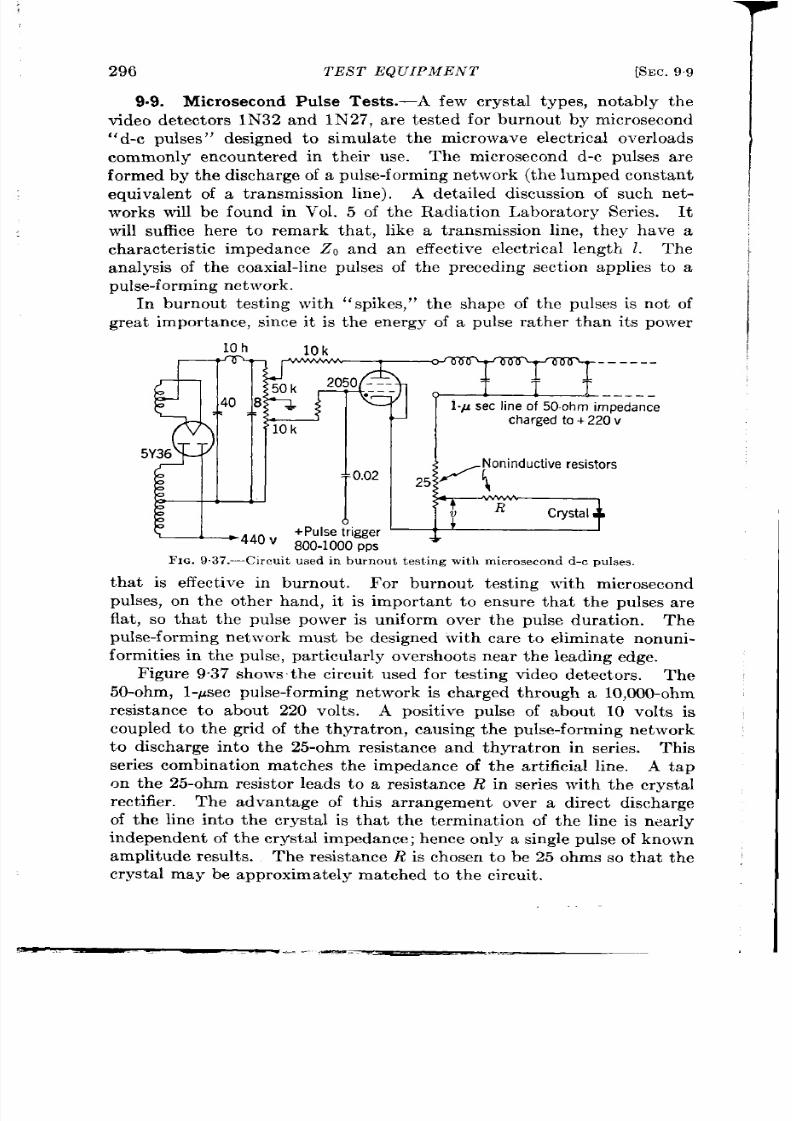
296
9.9. Micr os econd
TES T EQUIPMENT
[SEC. 99
Pulse Tests.—A few crysta l types, notably the
video detector s 1N32 and 1N27, a re t est ed for bu rnout by microsecon
“d-c pulses” designed to simula te the microwave el ct r ca l over loads
commonly encoun tered in their use.
for med by t he discha rge of a pulse-formin g n et wor k (th e lumped consta nt
equ iva len t of a t ransmission line).
A deta iled discussion of such net -
orks will be found in Vol. 5 of the Radia t ion Labora tory Ser es. It
will su ffice here t o remark tha t , like a t ransmission line, they have a
cha racter ist ic impedance 20 and an effect ive elect r ica l length 1. The
analysis of the coaxia l-line pulses of the preceding sect ion applies t o a
pu lse-f orming ne twork .
In burnou t test ing with “spikes,”
the shape of the pulses is not of
grea t impor tance, since it is the energy of a pulse ra ther than its power
10 h
1P sec
line of 50-ohm impedance
charged to+ 220 v
5Y36
,,
FIG. 9.37.—Cir cu it used in bu rn ou t t est in g wit h m icr osecon d d-c pu lses.
tha t is effect ive in burnout . For burnou t test ing with microsecond
pu lses, on the other and, it is impor t an t to ensure tha t the pulses a re
fla t , so tha t the pu lse power is un iform over the pulse dura t ion . The
pulse-forming network must be designed with ca re to elimina te nonuni-
for mit ies in t he pulse, par t icu la rly over sh oot s n ea r t he leading edge.
Figu re 9.37 show the circu it u sed for t est ing video detector s. The
50-ohm, l-psec pulse-forming n et wor k is ch ar ged t hrou gh a 10,000-ohm
resistance to about 220 volt s. A posit ive pulse of about 10 volt s is
coupled to the gr id of the thyra t ron , causing the pulse-forming network
to discharge in to the 25-ohm resist ance and thyra t ron in ser ies. This
ser ies combina t ion matches the impedance of the ar t ificia l line.
A tap
cm the 25-ohm resistor leads to a resistance R in ser ies with the crystal
rectifier.
The advant age of this a r rangement over a direct discharge
of the line in to the crystal is that the termina t ion of the line is near ly
independent of the crystal impedance; hence only a single pulse of known
amplit ude result s. The resistance R is chosen to be 25 ohms so that t he
crysta l may be approximate y matched to the circu it .
F.._
.— ___
—
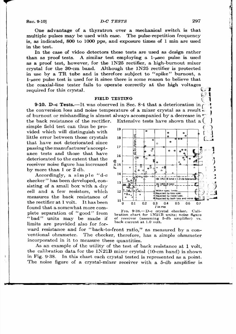
SEC.9-10]
D-C TESTS
297
One advantage of a thyra t ron over a mechanica l switch is tha t
mult iple pulses may be used with ease.
The puls e-r epet it ion fr equency
is, as indica ted, 800 to 1000 pps, and exposu re t imes of 1 min a re used
in the test .
In the case of video detector s these test s a re used as design ra ther
than as proof test s. A simila r t est employing a l-psec pu lse is used
as a proof t est , however , for the 1N25 rect ifier , a h igh -bu rnout mixer
crysta l for the 30-cm band. Although the 1N25 rect ifier is prot ect ed
in use b a TR tube and is therefore subject t o “spike” burnou t , a
l-psec pulse t est is used for it since there is some reason to believe tha t
the coaxia l-line t est er fa ils to opera t e cor rect ly a t the high voltages
r equ ir ed for t his cr yst al.
f;
,.~,
FIELD TESTING
(1
9.10. D-c Tests.—It was observed in Sec. 8.4 tha t a det er iora t ion in
f!
the conver sion loss and noise t empera tu re of a mixer crysta l as a resu lt E .
of bu rn ou t or mishandling is a lmost a lwa ys accompan ied by a decr ea se in’-
1
t he back resista nce of t he r ect ifier .
Extensive test s have shown tha t a ( )
simple field t est can thus be pro-
vided which will dist inguish wit h
lit tle er ror bet ween t hose cr yst als
tha t have not deter iora t ed since
pass ing t he manufa ct u r er ’s a ccep t-
ance test s and those tha t have
deter iora ted to the exten t tha t the
r eceiver n oise figu r e h as in cr ea sed
by more than 1 or 2 db.
Accordingly, a simple “d-c
sist ing of a small box with a dry
cell and a few resistors, wh ich
measures the back resist ance of
the rect ifier a t 1 volt . It has been
found tha t a somewha t more com-
plet e separa t ion of “ good” from
“bad” unit s may be made if
limits a re provided also for for -
19
t~
0
J
0
0
,a
0
~.l
18
0
3
0
0 00
[.4
$
()
~
0 0
17
D
0
d
i 0.:.
00 ~o 0
16 - ~
0
e
I
0
A
.s 15
k b ;0 ~: c, ~ ~e
&
14
12
.
. I
11
0 0.1
0.2
0.3
0.4 0.5
0.6
0.1
1 in ma
FIG. 9.35.—D-c crysta l checker . Cali-
bra t ion char t for 1N21 B units; noise figu re
of receiver (assuming 5-db amplifier ) vs.
back cur ren t at 1.0 volt .
ward resist&ce and for “ back-to-fron t ra t io,”
as measured by a con-
ven tion al ohmmet er .
The check r , t herefore, has a simple ohmmeter
incorpora ted in it to measure these quant it ies.
As an example of the u t ility of the test of back resistance at 1 volt ,
the ca librat ion data for the 1N21B mixer crystal (lO-cm band) is shown
in Fig. 9“38. In th is char t each crysta l tested is represen ted as a poin t .
The nois figu re of a crysta l-mixer receiver with a fi-db amplifier is

298
T ES T EQUIPMEN T [SEC.
910
plot t ed ver t ica lly, and the reverse cur ren t
at 1 volt k
plot ted h or i-
zont
a lly. Th e cr ysta ls r epr esen ted h er e wer e deliber at ely su bject ed
to a
su fficien t n umber of m icr osecon d d-c pu lses
to
det er ior a te t h m appr eci-
ably, on the average. A hor izon t a l line A is drawn at the 1N21B speci-
fica t ion limit cor re ponding to the acceptance limits on loss and noise,
and a second hor izon ta l line B is dr awn t o in dica te the above acceptance
limit plus 1 db, a toler nce tha t is a lways applied according to specifica-
t ion s on r emea su r emen t s.
The ver t ica l line C
at
0.125 ma was selected as the test limit for
the crysta l checker on the basis of these data for the 1N21B rect ifier .
Alt hou gh t he point s are well s ca t t er ed on the char t , it is apparen t tha t
F IG. 9,39.—C r cu it dia gr am of t he d-c cr yst al ch ecker .
the crysta ls accepted on the basis of the checker limit (i.e., the crysta ls
to the left of line C) are almost all less in noise figure than the specifica -
t ion plus tolerance limit (line B). Also the crysta ls r ejected (poin ts
to the r ight of line C) ar e almost a ll grea ter in noise figure than the limit
indicated by line B. Act ua lly t he sepa ra tion is even bet ter than indi-
cated, for , ou t of 200 1N21B units tested, on ly 139 are on the ch ar t; t he
remain ing 61 were r ejected both by the checker and by noise-figure te~ts
but were too h igh in reverse cur r en t
or
in n oise figu re
to
fa ll on the char t .
Fur thermore, it must be remembered tha t the units represen ted here
had all been par t ia lly dest royed in order to pr ovide calibra t ion data .
Before
these
crysta ls wer e burned
they
had been tested both by the
checker and by noise and loss measurements.
All were less in noise
figu r e t han the acceptance limit plus 1.0 db tolerance and all but 2 were
cor rect ly ind ica ted as “ good” by the check limit of 0.125 ma.
Cer ta in limita t ions of the ch ecker must be recognized.
It has
been
found to
give a
reliable test on ly for un its that
have at one
t ime pa ssed
t h e t es t specifica t ion lim it s
on loss
and noise; hence it cannot be used as a
su bst it ut e for these tests. Also, separate calibra t ion of the checker is
,.
SEC. 9.10]
DC TESTS
299
necessary for each crysta l t ype and the fact that a unit of one type passes
the check limit for a second type doe not , of cour se, imply tha t the
unit is an acceptable subst itu te for units of the second type.
Theelect r ic circu it of th echecker isshownin Fig. 9”39. In posit ions
1, 2, and 3 of the ganged five-posit ion switch , the checker is used as an
ohmmeter . In posit ion 1, t he ohmmeter is short -circu ited and the rheo-
stat is adjust ed to produce fu ll-sca le deflect ion of the meter .
The meter
dial has two scales, one reading direct ly in ohms. In posit ions 2 and 3
of the switch , t he dial reading indica tes, respect ively, the fron t and the
back resistances of the rect ifier .
In posit ion 4 the rheosta t is readju st ed
for fu ll-sca le deflect ion . Under this condit ion 1.0 volt is placed across the
crystal unit in the back direct ion .
In posit ion 5 the meter is in ser ies
with the crysta and reads on its second sca le, ca librat ed in milliamperes,
the back cur ren at 1.0 volt .
In calibra t ing the checker 200 unit s
of each type were used, 100 each from the product s of the two leading
manufacturers. Whereas, n genera l, a differen t limit was required
for e ch type, it was found that for a given type the same limit wou ld
usua lly apply to the product s of the two manufacturers. This was
found to be t rue for t he lo-cm-band types 1N21, 1N21A, and lN21B
and for th 3-cm types 1N23, 1N23A, and 1N23B. It was not , however ,
found to be the case for the 1N26, t he l-cm-band unit . The ca librat ion
procedu re was to measure each unit for conversion loss, noise t empera-
tu re, back cur ren t at 1.0 volt , and front and back ohmmeter resistances.
These measurements were made both before and aft er burn ing the unit s
with microsecond d-c pulses.
From the data for loss and noise, t he noise
figu r F of a crysta l-mixer receiver with an amplifier of 5-db noise figu re
was compu ted. This noise figu re F was then plot t ed for each crystal
aga inst t he back cu r ren t at 1.0 volt and a li it on the lat ter quant ity was
selected wh ich would divide the group including bu rned and unburned
unit s in to “good”
and bad” ca tegor ies determined by the noise-figure
accept ance limit plus a l-db tolerance. It was found that the addit iona l
requirement of a
“fron t resistance” less than 500 ohms and a ‘‘ back-to-
fron t rat io” of more than 10 sligh t ly r educed the number of false accept -
ances without appreciably increasing the number of fa lse reject ions.
The limit s on back cu r ren t at 1.0 volt for the var ious types are given
in Table 9.1 and the calibrat ion result s in Table 9.2.
TABLE 9.1.—AGCEPTANCEI,IMITSON BACK CURRENTAT 1.0 VOLT
Type
Acccp ta n cc Lim it , ma
1N21
0,40
1N21A
0.175
1N21B
0.125
1N23
0.40
IN23A
0.30
1N231t
0.175
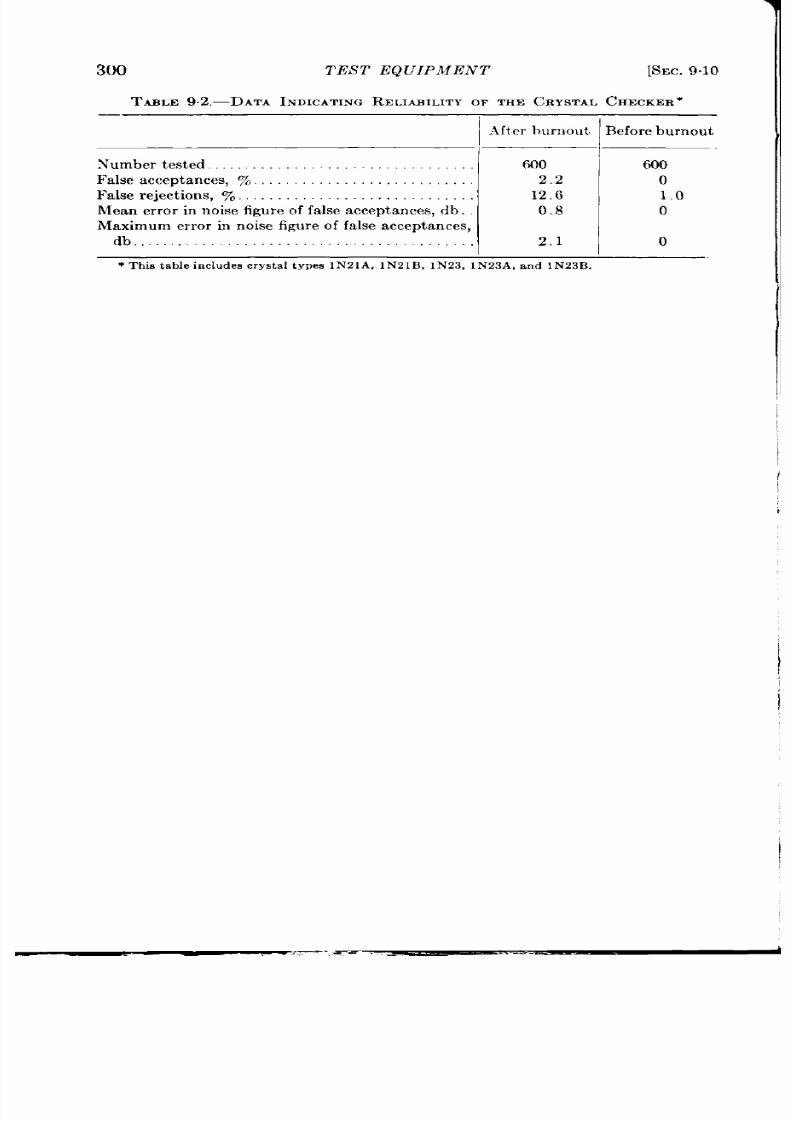
300
T ES T EQUIPMEN T
[SEC. 9.10
TABLE 92.-DATA INDICATINGRELIABILITYOF THE CRYSTAL CHECKER*
.ift er burnout Before burnout
Number tested 600
Ooo
False accepta nces, Yd, . .
2.2
0
False reject ions, Ye . . . . . . . . . . . . 12.6 1,0
Mean er ror in n oise figur e of fa lse acceptances, db. 0.8 0
Maximum er r or iu nois e figu r e of fa ls e a ccept a nces,
db . . . . . . 2.1 0
* This ta bleincludescrysta ltypes 1N21A,1N21B,1N23,1N23A,and1N23B.

f!
I
I
CHAPTER 10
MANUFACTURING TECHNIQUES
This chapter is limited to a descr ipt ion of represen t a t ive techniques
used in ma ufactur ing crystal rect ifier s for mixer applica t ions.
Th e
specia l procedures for making high inverse-volt age rect ifier s, low-level
detectors, and welded contact rect ifier s will be discussed in the chapt ers 4
devoted to those subject s.
The genera l processes for making high-qua lity rect ifier s a re now well
established. At presen t , these are: (1) pur ificat ion of the semiconductor ,
(2) con t roll d addit ion of a select ed impur ity t at produces the desired
proper t ies, (3) prepara t ion of an ingot from which the wafers used in the
car t r idge are cu t , (4) prepara t ion of the sur face of the wafers by a process
of polish ing, heat t rea tment , and et ch ing, (5) shaping and poin t ing the
cat whisker , (6) assembly and adjust men t , and (7) per formance-t est ing.
No at tempt will be made in this chapt er to descr ibe in det ail t he
procedu res that have been used successfu lly by all t he var ious manu-
facturers or to include procedures that t he au thors rega rd as obsolete.
Those descr ibed below may be regarded, however , as represen ta t ive of the
presen t sta te of the art . Alt erna t ive methods areincluded in some cases
to indicat e that no set of t echniques is t o be regarded as un ique.
PREPARATION OF THE SEMICONDUCTOR
10.1. Purificat ion of the Semiconductor .-Because the rect if ying
pr oper ty of t he sem icon du ctor is a ffect ed by min ut e qua ntit ies of impu ri-
t ies, t he fir st st p in t he ma nufactu re of r ect ifier s is t he pur ifica tion of t he
semiconductor . The degree of purifica t ion required depends to some
exten t on the method of prepar ing the ingot . The process of prepar ing
silicon in got s developed by t he Bell Teleph on e La bor at or ies (descr ibed i
Sec. 10.3) uses commercia l E lect romet silicon , with a purity of 99.8 per
cent . The method is such that the upper par t of the melt has the
required rect ifying propert ies The lower por t ion is discarded. Other
manufacturers, how ver , have been able to ut ilize the whole ingot by
u sin g t he h igh -pu rit y duPon t silicon .
Purification of
Silicon.—The method developed at duPont produces
high-p r ity silicon, excellen t for crystal rect ifiers, and uniform from
lot to lot . The pur ity is est imated from spect roscopic tests to be not
less than 99.9 per cent . Other impur it ies not detectable by spect o-
scopic means may be present , but if s they appear to have no adverse
301

302
MANUFACTURING TECHNI UES [SEC. 10.1
effect on t he quality or uniformit y of t he silicon.
In the ear ly stages of
developmen t on e lot of si icon wa s fou nd t ha t pr odu ced infer ior r ect ifier s.
This infer ior performance was found to be due to the presence of small
quant it ies of silica . When the silica was dissolved with hydrofluor ic
a cid, t he silicon r ega in ed it s u su al excellen ce.
The proce s developed by duPont is essent ia lly the reduct ion of
silicon t et ra ch lor ide wit h zin c.
The react ion takes lace a t a tempera -
ture (950°C) well below the melt ing point of silicon but well above the
boiling point of zinc, zinc chlor ide, and silicon tet rachlor ide. The zinc
ch lor ide formed in t he r ea ct ion a nd a ny excess zin c or silicon t et ra ch lor ide
, a re ca rr ied off as a vapor .
The silicon is deposit ed on the bot tom of the
r ea ct or chamber in t he form of needle-shaped cryst als.
A sketch of the genera l layout of t he equipment is shown in Fig. 10.1.
The main reactor chamber is a fused silica tube 6 ft long and 8 in. in
Asbestos
To condenser
pecking
*
Zn boir
M,
(
SiC14boiler
SiC14preheating tube
FIG. 10.1 .—Reactor chamber for prepar ing high-pur ity s ilicon .
diameter one end of which is fused over and carr ies two input pipes for
in t roducing the silicon tet rachlor ide and zinc vapor . A silica pla te is
clamped to the other end. This pla e carr ies an out let pipe tha t feeds
a silica pot collect or .
Zinc chlor ide and excess zinc set t le out in the
collector and the excess silicon tet rachlor ide passes through a out let
near the top to a condenser . The reactor is hea ted by ‘‘ globar” hea ters
(n ot shown in Fig. 10.1).
The whole appara tus is thermally lagged with
dia tomaceous ear th. The joint s a re packed with a paste made from
asbestos mixed to a st iff dough with water .
The zinc, a t leas 99.9 per cent pure, is bought in slab form. When
it is melted in a silica beaker , any oxide present forms a skin on the
surface. The molten zinc is poured from beneath this skin into the
boiler , from which the zinc vapor is fed to the reactor tube. Because
of it s low boili g poin t t he silicon t et ra ch lor ide is pr eh ea ted befor e en ter -
ing the reactor . This is accomplished by feeding it through long quar tz
tubes lying within the main heat ing chamber . The silicon tet rachlor ide
is bought a lready dist illed from an external supplier .
Redist illa t ion is
unnecessary.
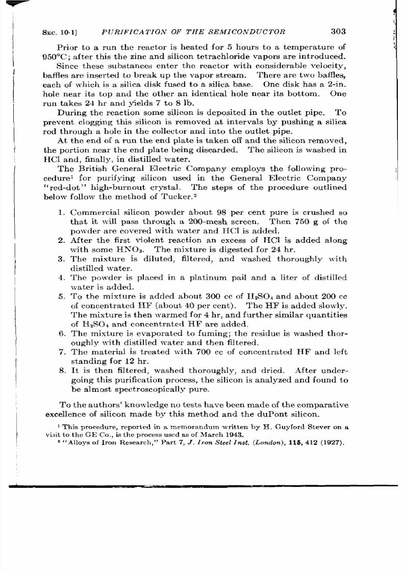
SEC.
10.1]
PURIFICATION OF THE SEMICONDUCTOR
303
Prior to a run the reactor is hea ted for 5 hours to a tempera tu re of
9500C; a ft er th is t he zin c a nd silicon t et ra ch lor ide va por s a re in tr odu ced.
iSince t hese su bstan ces en ter t he r ea ct or with con sidera ble velocity,
baffles a re inser ted to break up the vapor st ream. There a re two baffles,
each of which is a silica disk fused to a silica base.
One disk has a 2-in .
hole nea r it s top and the other an ident ica l hole nea r its bot tom. One
run takes 24 hr and yields 7 to 8 lb.
Dur ing the react ion some silicon is deposit ed in the ou t let pipe. To
preven t clogging th is silicon is removed at in terva ls by pushkg a silica
rod th rough a hole in the collector and in to the ou t let pipe.
At the end of a run the end pla te is taken off and the silicon removed,
the por t ion nea r the end pla te being disca rded. The silicon is washed in
HC1 a nd, fin ally, in dist illed wa ter .
The Brit ish Genera l Elect r ic ompany employs the ollowing pro-
cedura l for pur ifying silicon used in the Genera l Elect r ic Company
“red-dot ” high-bu rnou t crysta l.
The steps of the procedure ou t lined
below
1.
2.
3.
4.
5.
6.
7.
8.
follow ~h e m et hod of Tu ck er .2
Commercia l silicon owder about 98 per cen t pure is crushed so
tha t it will pass through a 200-mesh screen . Then 750 g of the
powder a re covered with wa ter and HC1 is added.
After the first violen t react ion an excess of HC1 is added along
with some HNTOS. The mixture is digested for 24 hr .
The mixtu re is dilu ted, filt ered, and washed thorough ly with
d is tilled water .
The powder is placed in a pla t inum pail and a liter of dist illed
wa te is a dded.
To the mixtu re is added about 300 cc of H. SO, and about 200 cc
of concen t ra t ed HF (abou t 40 per cent ). The HF is added slowly.
The mixtu re is then warmed for 4 hr , and fu r ther si ilar q ant it ies
of H&301 and concen t ra ted HF are added.
The mixtu re is evapora ted to fuming; the residue is washed thor -
ough ly with dist illed wa ter an d th en filter ed.
The mater ia l is t r ea ted with 700 cc of concen t ra ted HF and left
standing for 12 hr .
It is then filtered, washed thorough ly, and dr ied. .4fter under -
goin g this pu rifica t ion pr ocess, t he ~li~on is an alyzed and fou nd t o
be a lmost spect roscopica lly pu re.
To th e a uthors’ kn owledge n o test s ha ve been m ade of th e compar at ive
excellence of silicon made by this method and the duPon t silicon .
1This procedu re, repor ted in a memorandum writ ten by H. Guy ford Stever on a
visit t o t he G Co., is t he pr ocess u sed a s of Ma rch 1943.
‘ “Alloys of Ir on Resear ch ,” Par t 7, J . Ir on Steel I nst . (London ), 116, 412 (1927).
324
MANUFACTURING TECHN IQUES
[SEC. 10.1
Germanium.—Two met ods have been employed successfully in the
product ion of pure germanium for rect ifier use. The fir st of these
methods is the reduct ion of germanium oxide with hydrogen .
At the
suggest ion of Dr . Kar l Lark-Horovitz, the Eagle-P icher Company at
J oplin , Mo. developed a method for producing germanium oxide from
their standard ore residue. This source of supply made possible the
developm en t wor k on germanium at P ur due University, Gen er al E lect ric
Company, and Bell Telephone Laborator ies. The same company also
supplied germanium tet rachlor ide for the second method of prepar ing
pu re germa nium descr ibed la ter .
The procedures used by the var ious laborator ies for the reduct ion
of the oxide are essent ia lly the same.
The deta ils of t he Bell Teleph on e
Laborator ies procedura l are as fo lows. The reduct ion takes place in a
fur nace consist in g of a 4-in . silica tube 3 ft long which is closed at on e en d.
The ot er end is sealed to a metal head closed by means of a metal cover
that uses a lead gasket . Th e fur nace head ca rr ies h ydr ogen in let and out let
tubes t hrou gh which a cont in uous flovTof h ydr ogen is mainta ined du ring
the reduct ion process. The reactor tube is heated by a resi tance furnace.
A charge of 50 g of germanium oxide is placed in a quar tz boat 5 in. long,
1: in . wide, and 1 in . deep, nd the boat placed in a silica shield tube.
The furnace tube is then sealed, flushed ~vith hydrogen , and hea ted at a
temperatu re of 650°C for 3 hr ; th is is followed by a per iod of 45 min at
850°C. During the heat ing cycle the hydrogen flow is mainta ined at a
a te of 5 liter s per sec. By this method the germanium dioxide is
r edu ced t o germanium with an actual yield of 95 per cen t of t he th eor et ica l
yield. Since some loss probably occurs because of the evaporat ion
of GeO, the yield of 95 per cen t probably represen t s complete
reduction.
It has become common pract ice to test the pur ity of the product by
resist ivity measur emen ts on samples t aken fr om var ious par ts of an in got
made from the pure germanium, the resist ivity in genera l increasing
with the pur ity of the sample.
Theuerer and Staff r epor t that the
resist ivity of german um made from var ious lots of Eagle-P icher oxides
var ies from 4 to 12 ohm-cm.
Nor th ’ repor t s similar measurements on bulk resist ivity with values
ranging from 0.5 to 20 ohm-cm. The procedure used by Nor th for
reducing the oxide is as follows.
The oxide is placed in a fused silica
boa t within a closed thin-walled iron sleeve which is inser ted in an
Alundum-tube hydrogen furnace.
The iron sleeve is supplied with
I H . C. Th eu er er a nd J . H . 8ca ff, “Developmen t of H igh Ba ck Volt age Germanium
Rect ifier s,” NDRC In ter im Repor t No. 1, Con tr act OEMS1-1408, NOV. 21, 1944.
2 H. Q. Nor th , “K-band Germanium Crysta le, ” NDRC 14-328, GE Co., Mar. 26,
1945.

SEC. 101] P URIFICA 1710N OF THE SEMICONDUCTOR
hydrogen which is carefully dr ied and purified by passing
305
it through
act iva ted alumina, a copper purifier , phosphorous pentoxide, and a
liquid-air t rap. The reduct ion process is car r ied out in 15 hr at a temper-
ature of 65o”C; after this, melts f the germanium are made in a graphite
boat in the same furnace by heat ing to a tempera ture of 10150C for
20 min .
Nor th ’s resu lt s may be summar ized as follows. The bulk resist ivit y
of germanium fused in a hydrogen a tmosphere is cr it ically dependen t on
the amount of wa ter vapor present .
If the dew point is as high as 30”F,
resist ivit ies as high as 40 ohm-cm are obta ined.
Mor eover , va cuum
melts made in the presence of water vapor have yielded resist ivit ies as
high as 40 ohm-cm. Regardless of the ryness of the reducing hydrogen,
germanium
fused
in pure dry hydroge yields bulk esist ivit ies of 2
ohm-cm and below. Remelt ing in moist hydrogen ra ises the resist ivity
to the range of 10 to 20 ohm-cm. In the development work at Genera l
Electr ic, Nor th found tha t germanium of a bulk resist ivity of 5 to
30
ohm-cm a s sa tisfa ct or y for r ect ifier u se.
In t he secon d met hod, developed by du Pon t, 1high-pu rity germa nium
is produced from the tet rachloride in an oxygen-free atm sphere with
zinc vapor as the reducing agent . This is similar to their method of
pr odu cin g h igh -pu rit y silicon . Th e g&mar rium t et ra ch lor ide is obt ain ed
I
fr om t he E agle-P ich er Compa ny.
For th is second method the reactor is a 4~-in. silica tube 3 ft long
~
housed in a furnace of insulat ing br ick and heated by means of “ globars. ”
The germanium tetrachlor ide is preheated by passing it through 14 ft of
silica tubing, housed with in the furnace, before it en ters the reactor .
Zinc vapor from a silica flask boiler en ters the reactor through a jet
adj scent to the germanium tet rachl or iole jet , both of them mounted in
one end of the reactor tube parallel to the axis of the tube. Dur ing a
run the reactor tempera ture is mainta ined at 930”C, approximately
midway between the boiling point of zinc and the melt ing poin t of
germanium.
Germanium prepared by this method alloys with zinc at the tempera-
ture of the reactor , and the product recovered from the reactor may con-
ta n as high as 40 per cent zinc.
Most of this res dual zinc can be
removed by continuing the heat ing and passing iner t gas through the
reactor after the react ion has been completed. The product is then
t rea t ing it with hydrochlor ic acid until chemica react ion has ceased.
This removes all but about 0.2 per cent zinc, which can be removed by
1C. E. Rick a nd T. D. McKin ley, “ Sin ter in g or Melt in g of Bor on a nd Pr epar at ion
of H yper pu re German ium,” OSRD pr ogr ess Repor t NWP-P-W3K, Con tr act OEMsr
1139, Au g. 1 to Sept . 1, 1944.

I
306
MANUFACTURIN G TEC!HN IQ UES
[SEC. 10.2
vacuum melt ing. F llowing th is hy roch lor ic acid t r ea tmen t , t he
product is t r ea ted for 4 h r with conc nt r a t ed boiling hydrofluor ic acid to
r emove any silica presen t .
It is then washed and dr ied.
With the appara tus des r ibed above, two typica l runs yielded a tota l
of 7.2 lb of german ium in a tota l r eact ion t ime of 26 hr . A spect roscopic
analysis of the german ium gave an est imated impur ity of approximately
0.05 per cen t , in addit ion to the 0.2 per cen t zinc men t ioned above.
Resist ivity measu rement s of melt s made from this german ium gave
values in the r ange of 30 to 40 ohm-cm, and the rect ifica t ion character -
ist ics show that it is at least as good as tha t prepa red by the red ct ion
of the Eagle-Picher german ium dioxide.
As yet not enough lots of the
duPon t german ium have been prepa red to determine whether it is
super ior in uniformity to german ium prepar ed fr om the oxide.
There is some quest ion abou t t e va lidlty of the resist ivity as an index
of pu r ity. Theuer er and Scaffl poin t ou t that in one melt of duPon t
h igh-pu r ity germanium, the top par t of wh ich had a resist ivity of 120
ohm-cm by the standard poten t ia l probe method, ther e wer e severa l
sharply defined ir r egu lar lines runn ing ver t ica lly in the melt where
r egions ohmic character ist ics wer e found; adj scen t to these regions ther e
wer e obser ved a negat ive-r esist ance character ist ic c in the f orward dir ec-
t ion on the oscilloscope and a photo response having considerable sensi-
t ivity in the ult raviolet .
Similar effect s ave been observed in a melt of
german ium made from GeOz.
The Purdue Univer sity group found that resist ivit ies ca lcula ted from
spreading resist ance may be an order of magn itude lower than those
measur ed dir ect ly in a slab of h igh -resistance german ium, and they sug-
gest that r esist ivity ca lcula t ed from spreading resistance is a bet ter
indica t ion of pur ity. However , Nor th2 repor t s that consisten t r esu lt s
have been obta ined with resist ivity measuremen ts on large number of
in got s t rea ted iden tica lly.
10.2. Addit ion Agent s.—To obtain good rect ifica t ion character ist ics
a “ doping” agen t (a specified small quan t ity of a select ed impur ity)
must be added to the semiconductor , as has been poin t ed ou t in Chap. 4.
Up to now the par t icu lar agen t and the proper amoun t to use has for the
most par t been decided empir ica lly.
Addition Agent -s for Silicon .—Th e m ixer cr yst als t ha t h ave been man u-
factured in quant ity to da te h ve used either aluminum or boron as an
addit ion agent ; in some cases beryllium is a lso added. Either of these
when added t o silicon produces a p-type crysta l.
1H. C Theuerer and J . H. Staff, BTL Inter im Repor t No. 2, Cont ract OEMsr -
1408, Dec. 16, 1944.
2 op. @“t.
I
SEC. 10.2]
ADDI1’ION AGEN 1’S
3(I7
Aluminum was used as a doping agen t by the Br it ish Genera l Elect r ic
Company in t he ma ufactu re of red-dot crysta ls. In this company’s
procedure 0.25 per cen t by we ght of aluminum powder and 0.2 per cen t
by weigh t of beryllium are added to the silicon . Fox, Pearsa ll, and
Powelll found tha t the amount of a luminum and beryllium added is
not t oo cr it ica l. They found tha t good high-burnout crysta ls could
be made by adding about 0.4 per cen t of aluminum and 0.1 per cen t of
beryllium to the duPon t silicon .
Both of these addit ion agents a re
of the h ig est pur ity and are thoroughly mixed in a finely divided sta t e
wit h t h e silicon .
With t he Radia t ion La bora tory pr ocedu re of prepar in g
the ingot , t he beryllium serves to give a very solid ingot fr ee from cracks
and seems to con t r ibu te lit t le else of percept ible advantage. On the
other hand, Angello2, r epor t s a method of prepa r ing the melt withou t the
use of beryllium in which near ly all of the melt is usefu l. Angello used
the duPon t silicon with 0.5 per cent by weigh t of 99.9 per cent pu re
aluminum.
In 1942, du r ing the ea r ly days of crysta l resea rch , an exper imen ta l
stud y of the effect of var ious doping agents was made by th Univer sity
of Pen nsylva nia gr ou p.3
Because of the more recen t advances in the
melt in g t echniques and in making high-pu rity silicon , t he resu lt s of t hese
exper iment s a re now to be rega rded as main ly of qua lita t ive in t erest
Many elemen ts wer e found which produced good cur rent -volt age char -
a cter ist ics, but t he r -f per for ma nce was n ot r epor ted. Th e Pennsylvania
study repor t ed tha t the addit ion of 1 per cen t of boron to silicon gave the
except ion ally h igh con du ct ivit y of 2000 mho/cm , bu t t ha t n o r ect ifica tion
was observed. Theuerer4 la ter discovered tha t the addit ion of boron to
pure silicon in as small a quantity as 0.0005 per cent produces an ingot
tha t is remarkably uniform and excellen t for mixer crysta ls. Because of
its excellen t pr oper ties, combin in g h igh bu rn ou t a nd low con ver sion loss,
bor on -doped silicon h as la rgely su per seded a lumin um -doped silicon .
The amount of boron used is not cr it ica l and va r ies with differen t
manufacturers.
The Bell Telephone Labora tor ies have found the range
of 0.0015 t o 0.005 per cen t by weight sa t isfact ory; t he Radia t ion La bora-
tory procedure uses 0.003 to 0.006 per cent of boron and 0.02 per cen t of
beryllium, both added in powdered form. To add such small amounts
of boron , a mast r a lloy conta in ing 1.0 per cen t boron is fir st made.
1Marvin Fox, C. S . Pearsa ll, and Vigin ia P owell, “ Manu fa ct ur in g P rocedu re for
t he Ra dia tion La bor at or y H igh Bu rn ou t Cr yst als,” RL Repor t No. 501, Dec. 21, 1943.
2 S. J . An gello,
“ West in gh ou se Cr yst al Det ect or P ilot Sh op,” Resea rch Repor t
SR-176, Apr . 21, 1943.
3 F. Seitz, The Elect r ical Conduct ivityy of Silicon and Germanium,” NDRC
14-110, Un iv. of P en n., N ov. 3, 1942.
4H . C. Th eu er er , “ P repa ra tion a nd Rect ifica tion Ch ar act er ist ics of Bor o-Siicon
Alloys,” BTL Memor an dum MM-43-120-75, NOV. 2, 1943.
b
c,

308
MANUFACTURING TECHNIQUES [SEC. 103
This a lloy is th en used in th e appropr ia te quant ity for t he dopin g mater ia l.
E xper im en ts by C. S. P ea rsa ll a t t he Ra dia tion La bor at or y (u npu blish ed)
indica te tha t ga llium in quant it ies of 0.1 per cen t or less is promising as a
doping agen t . Time did not permit a defin it ive compar ison of rect ifie
per forma nce wit h t ha t of bor on -doped silicon .
No complet e syst ema t ic invest iga t ion of doping mater ia ls in which
the best techniques available have been used has as yet been made,
and it is possible tha t such an invest iga t ion would uncover other a lloys
a t least as good as the boron-doped silicon .
With the present st a t e of
knowledge such an invest iga t ion is a labor ious empir ica l procedure
involving not only the prepa ra t ion of melt s under a va r iety of exper i-
menta l condit ions bu also a sta t ist ica l analysis of the conver sion loss,
n oise t emper at ur e, a nd bu rn ou t ch ar act er ist ics of r epr esen ta tive r ect ifier s
made from the melt .
AaWtion Agents for Germanium. -Invest iga t ions of a la rge number of
doping agen ts for german ium mixer cryst a ls have been made by the Pur-
du e gr ou p. Amon g t he elem en t in vest iga ted wer e n it rogen , ph osph or us,
vanadium, a rsenic, columbium, ant imony, tan ta lum, bismuth , t in , iron ,
and nickel. Germanium doped with these elemen ts resu lt s in an n-type
semiconductor which shows good d-c cha racter ist ics.
However , r -f
measu remen ts made by the Purdue group in the 10-cm band showed tha t
man y of t hese a re infer ior , both in con version loss and n oise t emper atu re.
Amon g t hose dopin g a gent s which yield low conver sion loss crysta ls, t he
most promising on es a re a nt imony and phosphor us.
Extensive developmen t work y Nor th ’ has been ca r r ied ou t with
ant imony as doping agent . Melt s made with 0.2 to 0.5 a tomic per cen t
of a nt imon y h ave been fou nd sa tisfa ct or y.
Th es e melt s exh ibit r esist ivi-
t ies in the range from 0.003 to 0.01 ohm-cm. The best r ect ifier s made
with t hese crysta ls in th e 3. ‘2-cm band showed conver sion losses as low as
3.8 db with opt imum r-f and i-f match ing condit ions, a typica l sa pling
averaged about 6.5 db. The best noise t empera tu re measu red was 1.4,
but the average was around four t imes, a t a r ect ified cu r ren t of 0.6 ma and
with zer o d-c bias.
Nor th has a lso made melts using phosphorus as doping agen t . He
repor t s tha t no bet t er per formance has been ach eved than with ant i-
mony-doped germanium, and tha t the phosphorus-doped unit s appear
t o be m or e su scept ible t o bur nou t.
10s3. Prepara t ion of the Ingot .—The cryst a ls used in the rect ifier
ca r t r idge a re wafers cu t from an ingot made by the fusion and recryst a ll-
iza t ion of a mixtu re of the pure semiconductor and the appropr ia t e
quant ity of the doping agent . A good ingot is solid, fr ee from cracks, and
1H. Q. Nor th , “K-band GermaniumCrys ta ls ,”NDRG 14-328,GE Co., Mar . 26 ,
1945.

SEC. 10.3] PREPARA TIO.Y OF THE I,VGOT
309
character zed by un iformity of the requ ired elect r ica l proper t ies, or by a
u niform con tr olled va ria tion of t hese pr oper ties, t hr ou gh ou t t he in got .
The procedures used in the prepara t ion of the ingot by I’ar ious manu-
1
fa ct ur er s differ in t he followin g essen tia l r espect s:
1. The mechanica l deta ils of th e fu rna ce.
2. Th e hea tin g cycle used du ring t he melt ing and solidifica t ion .
3. The atmosphere in which the melt is made. Both vacuum furnaces
and fu rnaces in which a flow of selected gas is mainta ined a re used.
4. The na ture of the cooling process. The melt may be cooled in
place or may be progressively cooled from top to bot tom or vice
versa.
5. The crucible mater ia l used.
\
One or two typica l procedures tha t have proved successfu l will be
descr ibed. he furnace used by Fox and Pearsa ll a t the Radia t ion
Labora tory is a vac um furnace of the resistance type (see Fig. 10.2).
The fu rnace is evacua ted with a glass oil-diffusion pump (1) and a
mechanica l pump (2) tha t are capable of maintain ing a pressu re of 10–4
to 10–5 mm of Hg throughou t the melt ing opera t ion . The heat ing unit
~
(11) is a Nor ton Company Alundum elect r ic-fu rnace core No. 8871 cu t
to a length of 6 in . and wound with about 22 ft of 0.060-in . molybdenum
wire. This unit appears also at (7) moun ted inside the radia t ion shield
I
(6) which is a Nor ton Alundurn cor e of la rger size. The beryllia and
opa que quar tz bea kers which a re sh own at (5) h a e been su per seded, since
th is photogr aph was ta ken , by a bea ker ma de of clea r qu ar tz; it is believed
tha t the la t t er is less likely than the opaque quar tz to conta in impur it ies
such as TiOz. These beakers a re l; in. in diameter , 2* in . in length , and
hold abou t 50 g of du Pent silicon .
The bras por t ion of he system (12)
connect ing the diffusion pump to the heat ing chamber con ta ins a baffle
and a liquid-air t rap (3). The en t ir e brass por t ion of the syst m is
wa ter -cooled b means of copper tubing wound on the ou tside.
Th e
1 heat ing chamber is divided in to two par ts, and the photograph shows one
par t (8) swung open on a hinge. Thk por t ion carr ies a pyrex window (9)
th rough which the progress of melt can be observed. The thermocouple
tempera ture is read on a microammeter (4) and the pressure in the
system can be measured on a h!IcLeod gauge (10).
Dur ing the evacua t ion process, the power in the heat ing coil is
gradually increased until a ft er about l+ hr the melt ing tempera ture is
reached. The maximum power input is about 1.5 kw at 55 volts. The
tempera tu re result in from this input is somewha t h igher than the melt -
ing point of silicon . From this poin t the procedure va r ies with the
1
doping. For the a l minum-beryllium-doped silicon , the tempera tu re is
held constan t until the charge is completely molten . The power is then
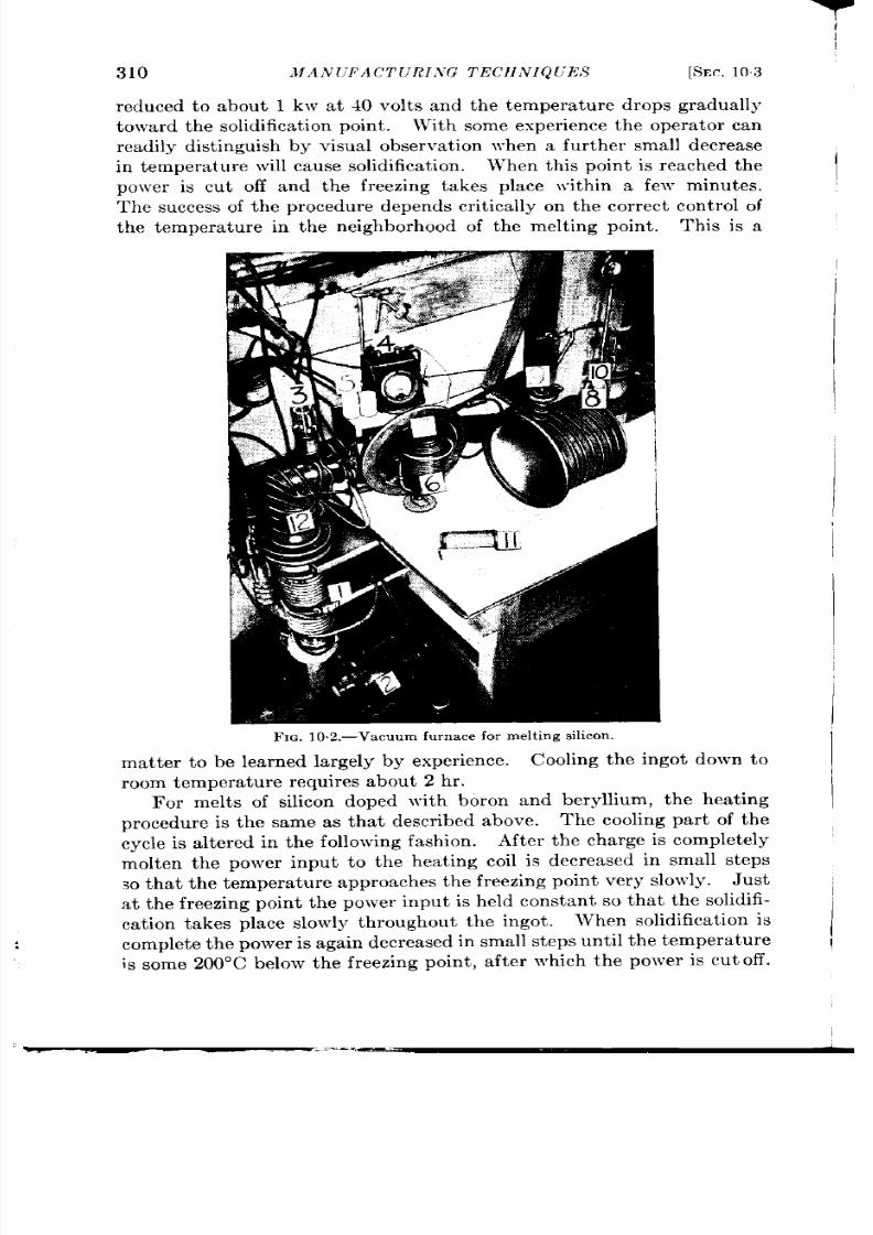
310
.lfA,V UFA CT lJ RI.T G TECJ IiVZQ [;E,S
[sm. 103
reduced to about 1 kw at 40 volts and the tempera tu re drops gradually
toward the solidificat ion poin t . With some exper ience the opera tor can
readily dist inguish by visual observa t ion when a fur ther small decr ease
in tempera ture will cause solidificat ion. }Vhen this poin t is rea ched the
po~ver is cut off and the freezing takes place \ vith in a few min tes.
The successor theprocedure depends crit ica lly on the cor rect cont rol of
the tempera ture in the neighborhood of the melt ing poin t . This is a
I
I
I
FIG. 10.2.—Vacuum furna ce for melt ing sil icon.
mat ter t o be lea rned la rgely by exper ience.
Cooling the ingot down to
room tempera ture requires about 2 h r .
For melt s of silicon doped with boron and beryllium, the hea t ing
procedu re is t he same as tha t descr ibed above. The cooling par t of the
cycle is a lt ered in the following fash ion .
Aft er t he charge is complet ely
molten the power inpu t to the hea t ing cod is decreased in small st eps
so tha t the t empera ture approaches the freezing poin t very slowly. J ust
at the freezing poin t t he power input is held constan t so that the solidifi-
ca t ion takes place slowly th roughou t the ingot . When solidifica t ion is
complet e the power is aga in decrease in small steps unt il t he t empera tu re
is some 200° C below the fr eezing poin t , a fter which the pow’er is cu t off.
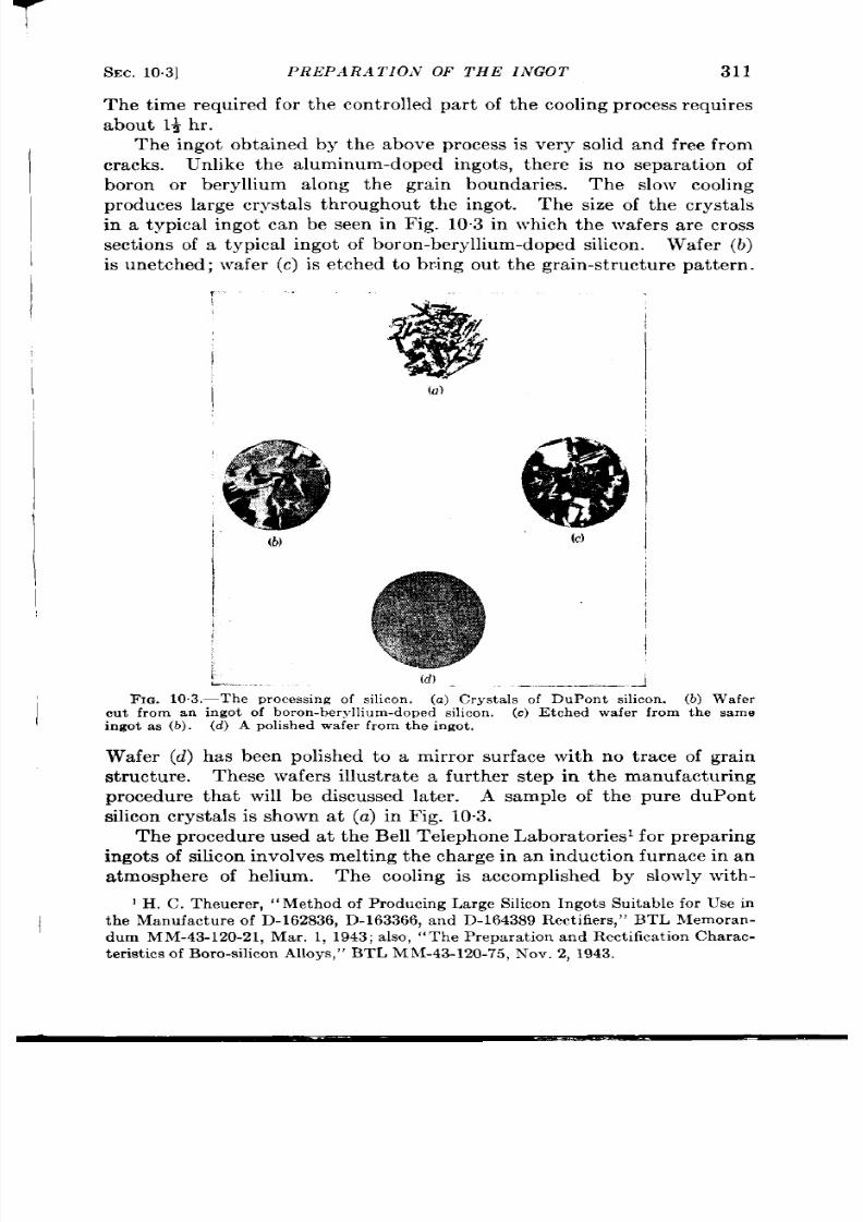
I
I
SEC.
103]
PREPARATION OF THE INGOT 311
The t ime requ ired for the con t rolled par t of the cooling process requ ires
abou t l+ hr .
The ingot obta ined by the above process is very solid and free from
cracks. Unlike the a luminum-doped ingots, th ere is no separa t ion of
boron or beryllium along the gra in boundar ies. The slow cooling
produces la rge crysta ls th roughou t the ingot . The size of the cryst ls
in a typica l ingot can be seen in Fig. 10”3 in which the wafers a re cross
sect ion s of a t ypica l in got of bor on -ber yllium-doped silicon .
Wafer (b)
is unetched; wafer (c) is et ched to br ing ou t the gra in -st ucture pat tern .
I
I
(b)
i
L..
(a)
(c)
( O_ . .__—
J
F IG. 10 .3.—The processing of s ilicon ,
(a) Crystals of DuPon t silicon . (b) Wafer
cu t fr om an ingot of boron -beryllium-doped silicon .
(.) Etched wafer from the same
in got a s (b). (d ) A polish ed wafer fr om th e ingot .
Wafer (d) has been polis ed to a mir ror su r face with no t race of gra in
structure.
These wafers illu st ra t a fu r ther step in the manufactur ing
procedure that will be discussed la ter . A sample of the pure duPon t
ilicon crysta ls is shown at (a) in Fig. 10.3.
The procedure used at the Bell Telephone Labora tor ies for prepa r ing
ingots of silicon involves melt ing the ch arge in an induct ion fu rnace in an
a tmosphere of helium. The cooling is accomplished by slowly with -
1H c, Th eu er er i‘Met hOdof P rodu cin g La rge Silicon In got s Su it able fOr U se in
t he Manu fa ct ur e of D-162836, D-163366, a nd D-164389 Rect ifier s, ” BTL Memor an -
dum MM-43-120-21, Ma r. 1, 1943; a lso,
“ Th e P repa ra tion a nd Rect ifica tion Char ac-
ter is t ics of Boro-s ilicon Alloys , ”
BTL Mh f-43-120-75, Nov. 2, 1943.

312
MA NUFACTURI,VG TECHN IQUES
[SEC. 103
drawing the melt from the heat -inducing field. The furnace is a silica
tube about 4 in . in diameter . The tube is s a led to a meta l head through
which the charge s in t roduced.
The head carr ies an ob ervat ion window
and a gas in let and out let for main t ain ing a flo~v of helium dur ing the
process.
A system of pulleys connected to the furnace head makes it
possible to raise the furnace through the h igh -frequency induct ion coil
at a prescr ibed ra te, either manually or by mechanica dr ive.
Th e
solidifica t ion then beginsat the top of he melt and progresses downward
through it as the furnace is raised.
Thecrucible isasilica cylinder 5in . ta lI and l~in . in diameter . The
crucible fits loosely inside a graphit e ea t er s ield in which hea t is gener -
a ted by the h igh -frequency field.
The crucible assembly rest s on a
I
F IG. 10.4.—Va ria tion in m elt in g pr act ice a nd it s effect on t he ph ysica l h ar act er ist ics of t he
s il icon ingot .
layer of No. 38 Alundum gra in and is su r rounded by an Alundum radia-
t ion shield. A silica feeding funnel r est s in the top of the crucible,
because the powdered silicon has a la rger volume than the liquid meta l.
The fu rnace head ca r r ies a silica poker t o facilita te feeding the silica
powder in to the crucible. The poker is in ser t e th rough a tubular hole
in the head and sea led gas-t igh t by means of flexible rubber tubing.
Aft er the cha rge is inser ted, approximately 55 min a re requ ir ed to
melt the cha rge and br ing the t empera tu re up to 1600°C. The fu rnace
is the ra ised unt il the top of the crucible is level with the top of the high-
fr equency coil. Aft er a per iod of abou t th ree minu tes in th is posit ion
the tube is ra ised ~ in . a t l-r ein in terva ls unt il it is 7 in . above the sta r t ing
posit ion . Aft er th i process the t empera tu re of the ingot has reached
700°C. It is then a llowed to cool to r oom tempera tu re. It is equally
sa t isfactory to ra ise the fu rnace cont inuous y a t the ra t e of ~ in . /r in by
means of the mechanica l dr ive.
I

SEC. 10.3]
PREPARATION OF THE INGOT 313
The ingots produced by the above process a re solid a d en t ir ely fr ee
from cracks. An etched ver t ica l sect ion th rough a typica l ingot is
shown in Fig. 10.4a . The fan like columnar crysta l st ructu re result s
from the empera tu re gradien t established wi h in the m lt in the cooling
process. The taper ing cross sect ion and rounded bot tom of the ingot
a re a resu lt of the expansion of the melt dur ing the freezing process.
Dur ing the last stages of the process the bot tom of the crucible bu lges
and the crucibles observed to r ise in the fu rnace.
Exper imen t s indica t e
tha t it is impor tan t , for the method descr ibed, tha t the melt ing t ime be
sufficient ly long for devit r ifica t ion of the silica cr cible to take place.
St ress relief on freezing then occurs in the crucible ra ther than in the
ingot . ith proper choice of the dimensions of the crucible and con t rol
of its devit r ifica t ion , the ingot breaks free of the crucible walls, and a
solid in got fr ee fr om cr ack s ~s obt ain ed.
Figure 10.4b shows a fractu red ingot obta ined at Bell Telephone
Labora tor ies when a melt was cooled by decreasing the power inpu t
gradually with the crucible in place in the furnace. It should be n ted
tha t fractu res of th is type have been successfu lly avoided in using the
Radia t ion Labora tory techniques, but it is not clear which differences in
techn iques a re responsible for the differen t result s obta ined in the two
laboratories.
The ingot s made by the progressive cooling process a re 4+ in . ta ll
with a mean diameter of Ii in . Per form nce tests show tha t the upper
2+ in . of these melts a re sa t isfactory for rect ifier units. In the lower
pa r t of the melt the impedance of the silicon increases and the r -f per -
form an ce is in fer ior . Abou t 2500 rect ifier un it s a re obta inable fr om ea ch
melt.
The method used by Nor th l for making ingots of an t imony-doped
germanium is as follows. A quar tz crucible ~ in . in diameter and 8 in .
long is suppor ted ver t ica lly in a quar tz fu rnace tube which is evacua ted.
A liquid-a ir t rap is used and the pre su re kept below 10–5 mm Hg dur ing
the melt ing and solidifica t ion process. The pu re germanium charge is
placed in the crucible and the ant imony is added aft er the germanium is
molten . This is accomplished by means of a small cup con ta in ing the
ant imony which is suppor ted above the crucible in a flexible manner by a
sylphon bellows. After th e german ium is molten the an t imony is shaken
in to the melt , wh ich is then slowly cooled. Average resist ivit ies of the
melts a re in the range of 0.003 to 0.1 ohm-cm.
In th is range the r -f
per formance is not cr it ica lly dependen t upon resist ivity. Higher resis-
t ivit ies increase the spreading resistance and cause h igher conversion
losses; ower r esist ivit ies ca use low ba ck r esist an ces a nd h igh er losses.
‘ H. Q. Nor th , “K-band Ger manium Crystals,” NDRC 14-328, GE Co., J far . 26,
1945.

I
I
314
MANUFACTURIN G T ECHN IQUES
[SEC.10.4
I
10.4. Polish ing, Heat -t rea tment , and Etching.-The processing of
the semiconductor , following the prepara t ion of the ingot , involves a
con t rolled procedure of polish lng, hea t -t rea tment , nd etchhg of the
crysta l wafer used in the rect ifier car t r idge. Our presen t understanding
of the effect s of these processes, in so far as they a re understood at a ll, has
been presen ted in Chap. 4; the purpose of th is se t ion is to descr ibe in
deta il typica l procedures for both silicon and germanium ”which have
been developed as a resu lt of the collect ive exper ience of the var ious
labora tor ies en ga ged in crysta l evelopmen t. Th eprocedu res for silicon
a ret hose for bor on -doped silicon , developed by Fox, P ea rsa ll, a nd P owelll
a t the Radiat ion Labora tory; some of the procedures are direct co ies or
modifica t ions of those used by other labora tor ies.
The processing of
germanium to be descr ibed is tha t used by Nor thz a t the Genera l E lect r ic
Research Labora tor ies.
Silicon .—The cylindr ica l ingot is first cu t in to th in circu lar wafers
about 1 mm th ick by means of a Rlmlock copper disk whose per iph ry
has a ser ies of closely spaced slots filled with diamond dust . Water is
used as a cooling agent . The saw marks a re removed by gr inding both
surfaces of the wafer with No. 600 Carborundum on a rota t ing copper -
lapping table wet down with water .
The next step is to polish the side of the wafer tha t is to be used for the
rect ifying con tact . The polish ing process is similar to tha t used at the
Bell Telephone Labora tor ies by Treut ing.3 Before the polish ing opera -
t ion begins, th e wa fer is cemen ted t o a copper block with cellu lose cement
so tha t it can be held easily. The polish ing is done dry on 000 emery
paper on a lap rota t ing at a speed of abou t 600 rpm. The polish ing lap
is “worked in” with a steel block and a mixture of light machine oil and
kerosene. The polish ing star ts with a small amount of the oil-ke osene
mixture, and as it proceeds, the paper becomes dry. This opera t ion
requires from 10 to 15 min. When fin ished, the polished su rface is an
ext remely good m ir ror wit h a bsolu tely n o t ra ce of gr ain -st ru ct ur e pa tt er n.
(See Fig. 10.3d.) This polish ing process differs from ea rlier techn iques
wh er e t he wet met allogr aph ic met hods u sed pr eser ved t he gr ain -st ru ct ur e
pat tern . Here the in tent ion is to produce a flow layer which erases all
eviden ce of gr ain st ru ct ur e.
After polish ing, the oil is r emoved by washing the wafer in t r i-
ch loroethylene. The cellu lose cemen t used to cemen t the wafer to the
meta l block is r em oved from t he wa fer by immersion in h ot con cen tra ted
I Ma rvin F ox, C. S. P ea rsa ll, a nd Vir gim a P owell, “Ma nu fa ct ur in g P rocedu re for
t he Ra dia tion La bor at or y H igh Bu rn ou t Cr yst als, ” RL Repor t N o. 501, Dec. 21, 1943.
z H . Q. Nor th , “I{-ba nd Germ anium Crysta ls,” NDRC 14-328, GE Co., Mar. 26,
1945.
3R . C. Tr eu tin g, “ P relim in ar y Developmen t of Impr oved Bu r nou t Silicon Con ta ct
Rect ifier s,” BTL Repor t MM-43-12(L53, May 18, 1943.

SEC. 10.4]
POLIS HIN G, H EAT -T REATMEN T
315
sulfuric acid, and the wa fer is afterwards thoroughly washed in dist illed
water.
After the wafer is cleaned, it is t rea ted by heat ing in a ir for about
half an hour at a tempera ture of 900° to 950°C; it is then removed from
th furnace and a r-quenched. The oxide layer thereby produced on
the surface is removed by etching the wafer in 24 per cent hydrofluor ic
acid for about 30 sec. Exper iments by M. Fox at the Radia t ion Labora-
tory show that the a tmosphere in which the baking takes place need not
be air or oxygen. Cont rolled exper iments, using identica l techniques,
show that the same rect ifier per formance can be obta ined when using
atmospheres of COZ, Hz, He, 02, or Nz for the heat trea tment of the
silicon.
The next step is the pla t ing of the unpolished side of the wafer so
I
tha t it can be soldered to the mount ing in the car t r idge. For th is
purpose nickel-pla t ing done according to the method used by Angellol
is sa t isfactory. The unpolished surface is prepared for pla t ing by
swabbing it with a mixture of 10 per cen t concent ra ted nit r ic
acid and 90 per cent of 48 per cen t hydrofluor ic acid applied with a
plat inum loop. The st rength of this solu t ion is adjusted so tha t the
surface rea ct ion proceeds very slowly while th e gra in-st ructure pat t rn
becomes more and more sharply defined. If the react ion proceeds too
rapidly or for too long an in terva l, a dark-blue surface layer is formed
wh ich in ter fer es wit h th e pla tin g oper at ion .
If the etching opera t ion is
stopped when small bubbles begin to form all over the surface, a sa t is-
factory etch is obtained. To obta in opt imum adhesion of the nickel
pla te the wafer should be washed and the back surface pla ted before it
dr ies. In the plat ing opera t ion the wafer is held in a clamp with bakelite
jaws so tha t only the unpolished side is in contact with the urface of the
pla t ing bath. Electr ica l connect ion to the wafer is made by a spring
con ta ct t o t he polish ed su rfa ce.
The plat ing bath is:
1. Ammon ium n ickel su lpha te
105 g per liter of water
2. Ammon ium ch lor ide
15 g per liter of water
3. Bone acid
15 g per liter of water
A cu rrent density of - t o 10-ma/cmz produces an adequate pla te in about
5 min at room tempera ture.
P roper plat ing of the wafer is important . Poor contact o the crysta l
wit h t he ca rt ridge may ca use excessive n oisin ess a nd er ra tic per forma nce
in t h e r ect ifier .
After the pla ted wafer is washed and dried, it is placed on a flat
cardboard surface and broken with a knife blade in to small pieces of
1
1S. J . Angello, “Westinghouse Cryst al Det ect or Pilot Sh op,” Resea rch Repor t
SF&176, Ap r. 21, 1943.
316
MANUFACTURING TECHN IQUES
[SEC. 10.5
suitable size for solder ing to th car t r idge component . It breaks up
easily a long th e gra in boundar ies; with ver y lit t le waste material.
Th e
advantages of this procedur over tha t of sawing the wafer in to small
squ ar es a re
1. Th e r esu lt in g pieces a re a lmost fr ee fr om gr ain bou nda ries beca use
t he br ea ks occu r a lon g t hese bou nda ries.
2. The waste of mater ia ls is considerably reduced. With this pro-
cedure one obtains 15 to 18 pieces la rge enough to use per square
cen t imet er of wa fer .
The pieces of cry ta l obta ined a re now soft -soldered to the car t r idge
stud or screw by means of a suitable solder ing jig. A suitable flUX is
st ain less-st eel Solder in g F lu x N ’o. 6.1
After the soldering process, the
silicon pieces ar e groun d down t o th e diameter of t he stud with a diamond
gr inding wheel.
Th e crysta l is given a final etch immedia tely befor e inser t ion in to th e
car t r idge. Thestuds onwhicht hecrys a lsa remounted are placed ona
plat inum screen and immersed in 48 per cent hydrofluor ic acid for 5 to
10 sec. This produces a mild elect rolyt ic act ion . Aft er the studs a re
washed they are ready for insert ion in to the car t r idge.
Gemzanium,-In the procedure used by Nor th’ for ant imony-doped
germa nium, t he in got is cu t in to wa fer s 0.020 in . t hick an d t hese a re gr ou nd
with 600-mesh Alundum under wa ter on a glass lap. The wafers a re
then pla ted ~vith rhodium and cut in to squares 0.070 in. on a side. These
are soldered to the ca r t r idge studs, which a re then mounted, 20 at a t ime,
on a jig for polish ing.
.4 wet polish ing wheel is used. There a re th ree
steps to the polish ing process: fir st , th e crysta ls ar e ground on a fine stone
to br ing all the sur faces in the same plane; they are then poli hed with
600-mesh Alundum on cloth ; and, fina lly, \ vith fine magnesium oxide on
cloth to give a high polish .
Heat it rea tment and etch ing appear to be unsuited to ant imony
doped germanium. Exper imen ts by N’or th show that hea t t rea tment in
air , followed by an etch to remove the oxide, produces a germanium
su rfa ce wh ich wh en pr obed sh owed a lmost sh or ~cir cu it ch ar act er ist ics.
THE CAT WHISKER
10.5. Whisker Materials. —Pr oper t ies to be con sidered in the ch oice
of \ vhisker mater ia ! are it s work funct io and its mechanica l proper t ies.
It should be a hard meta l so tha t the poin t is not excessively fla t tened
by the pressure required for good rect ifying character ist ics; it must be a
meta l tha t can be fabr ica t d in wire form and cr imped to the desired
:
1Obtainedfrom the Colonial Alloys Co. of Philadelphia,Pa .
,
2Lot , ant .

SEC. 10J ]
WHISKER MA TRRIALS
317
wh isker sh ape; a nd it sh ou ld h ave su fficien t ela st icit y t o g!vc mech an ica l
st abilit y for fea sible wir e sizes.
The wor k funct ion of the metal is onc of the quantit ies tha t dr+wninc
the nature of the barr ier a t the meta l-semiconductor contact , as wcs
expla ined in Chap. 4.
Th ere wesa \ v tha t , for rect ifica t ion to occu r, the
work funct ion of the metal must be less than tha t of a p-type semicon-
ductor ; for n-type semiconductors the rever se is t rue. Moreover , the
I
height of the barr ier in the semiconductor depends on the difference in
wor k fu nct ion between t he met al a nd sem icon du ct or .
In the case of silicon, J . A. Becker ’ repor ts tha t character ist ic volt -
ampere curves obta ined from various metal-to-silicon poin t contacts in
a ir do not exhibit differences tha t can b readily associated \ vith differ -
ences in the work funct ions of the various metals as determined by
vacuum thermion ic measu r emen t s.
This is not surprising, for it is well
known that work funct ions are st rongly dependent on the presence of
a bsor bed ga ses or ot her su rfa ce con tamin at ion s.
It is only when metal
contacts are evapora ted in vacuum that any reasonable correla t ion is
fou nd between rect ifica tion ch ar act er ist ics and metal ~vor k fun ct ion . In
the light of present knowledge the ~~hisker mater ial does not play as
impor tant a role in the rect ifica t ion picture as one would expect from
theoret ical considerat ions.
F or t hese rea son s t he ch oice of wh isker materia l has be n an empir ica l
on . For silicon rect ifiers, tungsten has been almost universally used.
The Brit ish-Thomson-Houston Company prefers molybdenum-tung-
sten, wh ch they have found to be more consisten t in quality than pure
split -free tungsten . Other manufacturers have found commercial tung-
sten sat isfactory. The mechanical proper t i s of tungsten are well
su it ed t o wh isker fabr ica tion .
Plat inum-ruthenium whiskers have been found to give somewhat
h igh er ba ck r esist an ces t ha n t un gst en on es in germanium m ixer r yst als.z
The pla tinum is a lloyed with 10 per cent ru thenium, to increase the
hardness.
The choice f whisker -wire size is determined largely by the force
required on the contact poin t . In the 10-cm band, where rela t ively large
contact areas are desired and ela t ively large forces are consequent ly
n ecessar y, 8-roil wires h ave been u sed for h igh-bu rn ou t r ect ifier s. Com-
mercia l low-conversion-loss nits w th good burnout proper t ies are
or dkr arily ma de with 5-roil wir e in t he cer amic ca rt ridge for 10- and 3-cm
use. In the coaxia l car t r idge, where the whisker space is very small
and th contact force small, wires 2 roils in d ameter have been found
satisfactory.
I Private communicationto the Radiation Laborat ory,Nov. 9, 1942.
t Private communicat ionfrom H. Q. North.

318 MANUFACTURING TECHNIQUES
[SEC. 10.6
1006. Fabrica t ion of the Whisker .-T e fabr icat ion of the whisker
involves th ree processes: (1) forming the whisker poin t , (2) cr imping
the wire to the desired shape, and (3) solder ing or welding the whisker
to the meta l ca t r idge component .
In actual pract ice, the order of
opera t ions var ies from on e manufacturer t o another .
For mechanica lly
formed poin ts, the poin t ng is usually done before the cr imping.
Form ing the Whisker
Point . —Conica l poin ts ar now almost uni-
ver sa lly u sed in commercia l r ect ifier s.
At on e t ime wedge-sh aped poin ts
wer e t hou gh t t o con tr ibu te t o t he h igh -bu rn out pr oper ty, but exper im en ts
I
i
I
A
a)
A
b)
FIG. 10.5.—E ffect of
elect rolyt ic polish in g on
contour of ground tung-
sten poin ts. (a ) Ground
point. (b) Ground and
elect r olyt ica lly polis hed
point.
Doin t cont act . The
by Fox and Pearsa ll a t the Radiat ion Labora tory
have shown that for equal areas of contact noth ing
is to be gained from a knife-edge ccntact .
The conical poin t may be formed either by
elect r olyt ic method . 1
In the mechanical method the wire is held
against the grinding wheel at an appropr ia te angle
by a rota t ing pin vise, the axis of rota t ion being
in a plane perpendicular to tha t of the gr inding
stone. The included angle of the cone is not
cr it ica l; an appropr ia te value is in the neighbor-
hood of 70° to 80°. The diameter of the poin t of
the cone is usually less than 0.0001 in. The con-
tact area will be larger than this, for the poin t
fla t tens when it is pressed against the silicon . A
pr oject ion m icr oscope ca n con ven ien tly be u sed t o
inspect the poin t for flaws.
In some in st an ces la rge va lu es of noise t emper a-
ture have been correla ted with microscopic
ir regular it ies in the geometry of the tungsten
grinding process may leave irregular it ies in the
~or of grinding mark; or bu~rs a t the poin t . .kn elect rolyt ic polishing
process has been used by the Western Elect r ic Company to remove these
irregula r it ies. This process, a repor t ed by Pfann2 gives the poin t t he
desired contou r and sur face smoothness.
The process consist s of making
the poin t a odic in a solu t ion conta in ing 25 per cen t by weight of potas-
sium hydroxide and applying O.8 volt for 2 sec followed by two successive
flashes of 0.2-sec dura t ion at 2.0 volt s.
A number of poin t s may be
connect ed in para llel and polished simultaneously. The ca thode is a
1 J . R. Woodya rd,
‘(Not es on Cr yst al Det ect or s,” Sp er r y Res ea rch La bor at or ies
Repor t 5220-110, Apr . 6, 1943; W. G. Pfann ,
“E lect rolyt ic P oin tin g of Tu ngst en
Con ta ct Wir e in Silicon Rect ifier s,” BTL Repor t MM-43-120-73, J u n e 29, 1943.
2W. G. P fa nn , “E lect rolyt ic P olish in g of Tu ngst en P oin ts in Silicon Rect ifier s,”
BTL Repor t, Ca se 24026, Dec. 3, 1942.
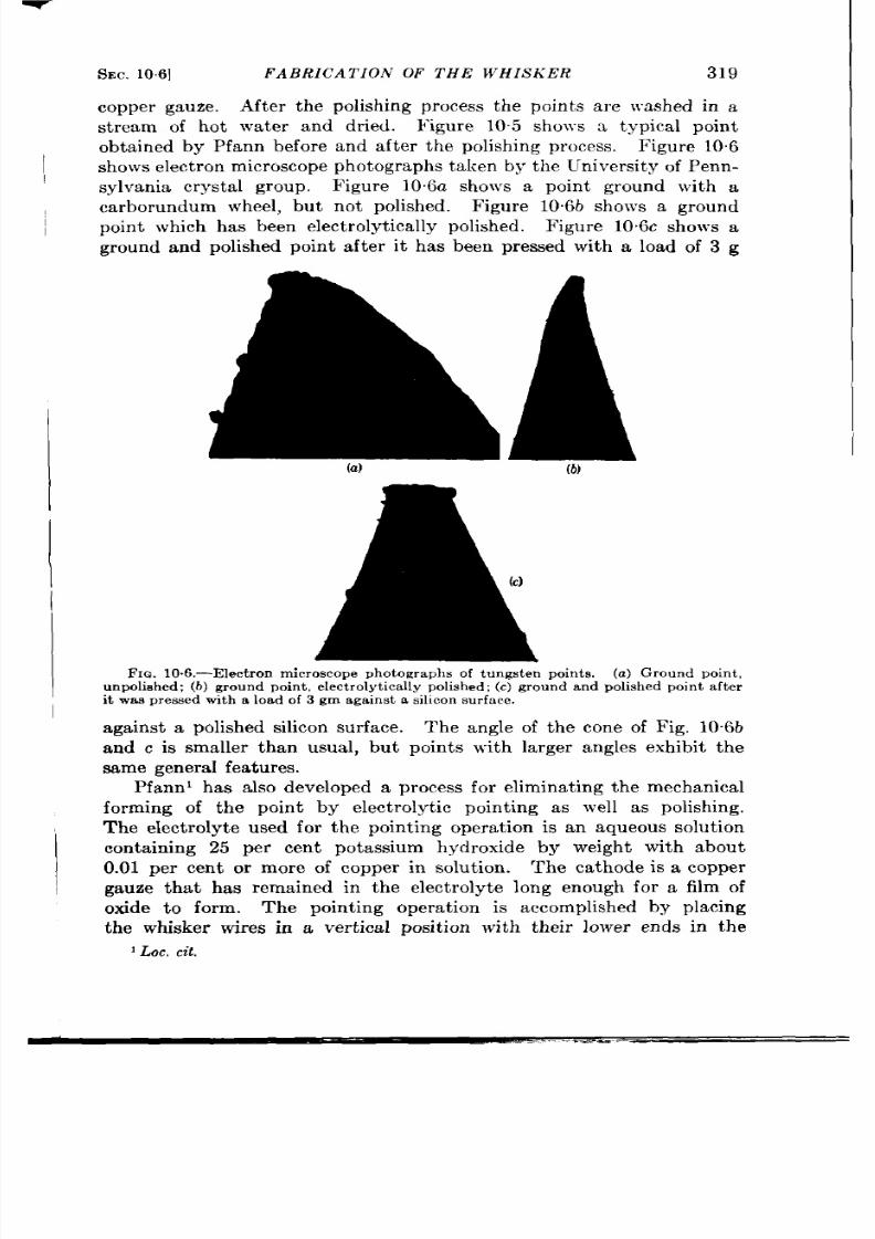
SEC.
106]
FABRICATION OF THE WHISKER
319
copper ga ,uze. After the polish ing process the poin t s a r e washed in a
st ream of hot wa ter and dr ied. Figure 105 shows a typica l poin t
obta ined by Pfann before and a fter the polishing process.
F igu re 10.6
shows elect ron microscope phot ograph s t aken by t he University of Penn-
sylvania crysta l gro p. F igu re 10.6a shows a poin t ground with a
Carborundum wheel, bu t not polished. F igu re 10.6b shows a ground
poin t which has been elect rolyt ica lly polished. Figure 10%c shows a
ground and polished poin t after it has been pressed with a load of 3 g
(a)
(b)
FIQ. 10.6.—Elect ron microscope photographs of tungsten points. (a ) Ground point ,
unpolished;
(b)
gr ou nd poin t, elect rolyt ica lly polish ed; (c) gr ou nd a nd polish ed poin t a ft er
it was pressed with a load of 3 gm against a silicon sur face.
a ga inst a polish ed silicon su rfa ce.
The angle of the cone of Fig. 10.6b
and c is smaller than usua l, bu t poin ts with la rger angles exhi it t he
same gen er a l fea t ur es.
Pfann’ has a lso developed a proce s for elimina t ing the mecha ica l
forming of the poin t by elect rolyt ic poin t ing as well as polishing.
The elect rolyt e used for th poin t ing opera t ion is an aqueous solu t ion
conta in ing 25 per cent potassium hydroxide by weigh t with about
0.01 per cen t or more of copper in solu t ion . The ca thode is a copper
gauze tha t has remained in the elect rolyt e long enough for a film of
oxide to form. The poin t ing opera t ion is accomplished by placing
the whisker wires in a ver t ica l posit io with their lower ends in the
1Lot, d.

-
320 J IA.Y L-FACT L’RING T hCHAT IQUES
[SEC. 106
elect rolyt e and applying 1 volt unt il t he cu r ren t drops to a value between
0.25 and 0.30 ma; for poin t s having a radius of cu rva ture of 0.0003 in .
the shutoff cu r r en t a lways falls ~~ith in th is r ange. The poin t ing process
A
(al
A
b)
FIO. 10.7.—Poin t con -
tours. (a ) Elect rolyt ic
point. (b) Ground and
electrolytically
polished
point . Radius of cu rva-
ture at t ill is 0.0003 in . in
each.
is then followed by polish ing flashes as previous y
descr ibed. Figu re 10.7a sho~vs an elect rolyt ic
poin t made by I?fann , and Fig. 107b shows for
compar ison a ground and elect rolyt ica lly polished
point.
The drop in cu r ren t at constan t voltages
ar ises fr om the decrease in wet ted area as the
tungsten is dissolved and from the polar iza t ion
at the wires. The shaping of the poin t depends
on the format ion of a meniscus of a suitable shape
about the ~vir e. The potassium hydroxide
solu t ion specified pr odu ces a sa t isfactory meniscus
for 5-roil ~vires, and the addit ion of the copper
to the solu t ion produces the requ ir ed adhesion of
the liqu id to the wire. Copper gauze is the on ly
ca thode mater ial tha t has been found sat isfactory.
The concen t r a t ion of potass um hydroxide i
not cr it ica l, la rge changes having lit t le effect on
the con tou r of the poin t ; the va lue of the shu toff
cu r r en t increases with i crease in concent r a t ion .
By th is pr ocedure as many as 100 wires have
been poin t ed in a single opera t ion , t e total t ime
requir ed being abou t one-ha lf hour .
The method provides a means for
accura tely con t rolling the length of the whisker assembly. For th is
pu rpose the wires are soldered t the ca r t r idge pin and cr imped pr ior to
the po n t ing opera t ion . Since the poin ts a lways form just below the
sur face of the solu t ion , uniformity of
le gth can be obta ined by un iform moun t -
Metal.cartridge
omponent
imz of the whisker assemblies in the holder \
of t h e elect r olyt ic cell.
isker
The Whisker Shape.— he whisker is
ben t to the desired shape by means of a
cr imping jig. The genera l shape of
~rhisker commonly used for the ceramic
car t r idge is shown in Fig. 10.8. Deta ils
on size and curva ture of the loops and the
FIc. 10.S.—lvhisker assemblyfor
th e ceram iccar tr idge.
over-a ll length of ,the whisker , toget her
with the in ternal geomet ry o the ca r t r idge, affect the r -f impedance of
the unit in a complica ted way; the deta ils of the design have therefore
been wor ked ou t empir ica lly by the individual manufacturer . The over -
1

SEC. 106]
FABRICATION OF THE WHISKER
321
all whisker length used by var ious manufa turers lies in the range from
about 0.1 to 0.15 in . and in product ion th is length is, of cour se, kept as
near ly constant as possible for a given car t r idge design .
Th e dou ble-
loop st ru ctu re ser ves as a spr ing whose compression pr ovides t he con tact
force; it a lso provides mechanica l stabi ity by mainta in ing the con tact
force perpendicula r to the crysta l su r face when the spr ing is
compressed.
Th e wh isker assembly for t he Radia t ion Labora tor y coaxia l car tr id e
is shown in Fig. 10,9. The single-loop whisker is commonly used for
th is type of car t r idge, in which it is desirable to keep the whisker size
to a minimum.
The effect s of in terna l geometry of the ca r t r idge on r-f
impedance is pronounced in th is type of ca r t r idge; the dimensions of
the Radia t ion Labora tory whisker
o,o1o-
assembly a re t her efore in clu ded in
F ig. 10.9, a nd t hose of t h e r emainder
0.015“
of the car t r idge n Fig. 10.13. As
was ment ioned in Sec. 10.5, 2-roil km
tungsten wire
is used for the ~
whisker . Stability of the contact is
achieved by making one arm of the
Spotweld
loop lon ger t ha t he ot her , a s sh own
in Fig. 10.9. his whisk r design is
Center
simila r, except for som e modifica -
conductor
tion
in dimensions, to tha t
ofcartridge
developed ear lier a t the Bell Tele-
phone Labora tor ies.
Mountinu the
Wh isk er .—In t he
ceramic ca r t r idge it is standard
FTQ. 10.9. —l17h is ker a ss embly for t h e Ra di-
t ion La bor at or y coa xia l ca rt ridge.
pra ct ice t o solder th e whisker to th e
ca r t r idge componen t .
Both Bell Teleph on e Labora tor ies and West ing-
house Research Labora tor ies’ have successfu lly used a hot -dip method
in which the tungsten wire is coa ted with an alloy of 69 per cen t gold, 6
per cen t pla t inum, and 25 per cen t silver . The wires a re readily wet t ed by
th e a lloy, which forms a th in a dheren t coa ting tha t can be easily soldered.
Nickel-pla tin g t he t un gst en h as a lso been fou nd sa tisfa ctory.
The shank of the whisker is soldered in to a hole in the meta l end piece
of the ca r t r idge (see Figs. 2“2 and 10.10), a lignment being mainta ined
dur ing the process by suitable jigs.
Aft er solder ing, the assembly is
in spected for a lignment of th e whisker axis with th e axis of th e ca rt r idge.
With t he excellen t crysta ls n ow available, “hu ntin g” for a sensit ive poin t
is n o lon ger con sider ed good pr act ice.
In the Radia t ion Labora tory coaxia car t r idge, the whisker is spot -
1S. J . Angello,WestinghouseResearchReport SR-176, Apr. 21, 1943.
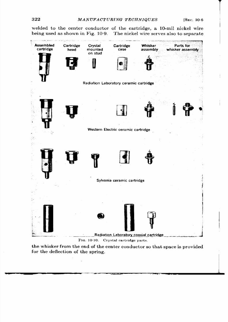
322 MANUFACTURING TECHNIQUES
[SEC.
106
welded to the cen ter conductor of th e ca r t r idge, a 10-mil n ickel wire
being used as shown in Fig. 10.9. The n ickel wire serves a lso to sepa ra te
.!
w
.
. ,.
. .. .,. . .... ... . . .
Assembled
Cartridge Crystal
y
Cartridge
Whisker Parts for
cartridge
head
mounted
case
assembly
whisker assembly ~
on stud
Uah
Radiation Laboratory ceramic cartridge
!
, .
I ?
:.
.,
R
.. .. . .. .
——
Western Electric ceramic cartridge
,
Sylvania ceramic cartridge
.$
i
[
“IY
!
i
_.>
@
/
,
t
:_.._Rall?ti_ln.L?4&rA!om coaxial c@Mge____ ~
J
FIG. 1010. Crysta l car t r idge par ts,
the whisker from the end of th e cen ter con ductor so that space is provided
for t he deflect ion of t he spr in .
I
I

SEC. 107] THE CERAMIC CARTRIDGE
323
ASSEMBLY AND ADJUSTMENT OF THE CARTRIDGE
10.7. The Ceramic Car t r idge.-Car t r idge par t s for represen ta t ive
ceramic car t r idges are shown in the top th ree r ws of Fig. 10.10. The
Radia t ion Labora tory ceramic car t r idg shown at the top is similar to
t ha t developed a nd ma nu fa ct ur ed by t he West in gh ou se E lect ric Cor por a-
t i n . 1 The other two car t r idges shown n the figure a re manufactured by
Sylvania Elect r ic Products, Inc. and the Western Elect r ic Company as
indicated.
Al t hese ca rt ridges meet t he JAN specifica tion s on external
dimensions but differ in st ructure because of the differen t mechanisms
used for adjustment of the contact poin t .
Cr oss sect ion s of a ssembled
car t r idges were shown in Figs. 2.2 and 2.4, Sec. 2.1.
The proper t ies required of the car t r idge case are, in addit ion to
insula t ion of the termina ls, low loss a t microwave frequencies and
mechanical st rength and r igidity
over the t empera tu re range from
about —40° to + 100”C. It must
a lso be made of a mater ia l tha t can
be fabr ica ted with t he close dimen-
sion al t oler an ces r equ ir ed (see Fig.
D. 1). Ceramic
mater ia ls meet
these requ irement s and a re now
Tohorizontalplates
of
oscilloscope
F]c. 10.11.—Circuit used for viewing the
r ect ifie r cha ract er is t ic on an oscilloscope.
un iversa lly used for th e purpose. Specifica lly, stea tite ceramics such as
Alsimaga 196 or 211 a re excellen t cer amics for th k pu rpose.
The J AN specifica t ions requ ir e tha t the meta l par t s, usua lly made of
brass, be pla ted with silver or gold.
The car t r idge is assembled by screwing the head and pin t ight ly in to
the ceramic case, which is th readed on the inside. A cemen t such M
orange shellac is applied to the par t s to make the join t t igh .
The adju tment of the Radia t ion Labora tory car t r idge is as follows.
Aft er the fina l et ch , the crysta l stud is inser ted in the car t r idge and
clamped light ly with the set screw in the side of the ca r t r idge head.
The car t r idge is then placed in a clamping device where the pressu re
from a mi rometer screw advances the stud toward the whisker poin t
a ga in st t he mech an ica l r esist an ce of t he set scr ew.
Electr ical connect io=
a re made to the head and pins of the ca r t r idge so tha t either the bac~
or t e fron t resistance an be measured in the neighborhood of 1 volt ,
or t he char acter ist ic cu rve obser ved on an oscilloscope.
For the la t t er
pu rpose a cir cu it simila r to tha t shown in Fig. 10.11 is used. A 60-cycle
a-c volt age (about 0.5 volt rms) is applied to the pr imary terminals of a
t ransformer (or Var iac), whose voltage output is connected to the rect i-
1S. J . Angello, West inghouseResearch Report SR-176, Apr. 21, 1943.
2Obtainedfrom the AmericanLava Corp., Chat tanooga,Term.

324
M.4NUFA CT URING TIICIIN IQUES [SEC. 10.7
fier C
in ser ies with the resistor R.
A
suitable value
of R is 10-to
20
ohms.
Once contact is established, the pressure is increased unt il a prede-
termined character ist ic is observed on the oscilloscope. In this stage
the fron t resistance, measured at a few tenths of a volt , is between 300
and 400 ohms, and the back resistance is about 10,000 ohms. The
car tr idge is t hen “ ta pped”1 light ly
J udiciou s ta pping causes t he fr on t
resistance to drop to between 200 to 300 ohms and the back resistance to
increase to between 20,000 to 100,000 ohms. (These values a re for an
applied poten t ia l of a few tenths of a volt . ) Before tapping, the oscillo-
(a)
(b)
FIG. 1O.12.—D-C character ist ic cu rve as seen o,n an oscilloscope. (a ) Before tapping;
(b) a ft er t app ing.
scope presen ta t ion appears as in Fig. 10.12 at (a). The sloping por t ion
of the curve breaks away grad a lly fr om the nonconduct ing r egion and
the slope of the curve increases with increasing forward voltage. Tapping
ligh t ly a few t imes produces the curve shown in F ig. 102 at (b). The
break in the curve is more sharply defined and the cu rve takes on a
constan t slope with increased volt age.
At th is stage fu r th er t apping
has lit t le effect on the character ist ic.
As a fina l step the set screw in the
car t r idge head is screwed in t ight ly.
~- amount f tapping done in the adjust ing of the contact is a
mat ter of the opera tor ’s judgment and exper ience.
In addit ion to the
changes in the character ist ic cu rve ment ioned, tapping has been observed
in som cases to decrease the noise temperatu re of the rect ifier . The
crystal groupz at the Univer sity of Pennsylvan ia has conducted con -
t rolled exper imen ts wher e tapping was simula ted by taking the con tact
1 ‘‘ Ta ppir rg” mea ns pr odu cin g mech an ica l sh ock by lows of a ligh t m allet .
z A. W. Lawson , P. H. Miller , L. I. Scht i, and W. E. Stephens, “Effect of Tapping
on Ba rr ier Ca pa cit an ce,” hTDRC 14-181, Univ. of P en n., Sept . 1, 1943.

d
,
SEC. 10.7]
THE CERAMIC CARTRIDGE
325
poin t th rou gh
one or
more loading cycles, and measuremen ts of capaci-
tance were made dur ing the process. They observed that this process
in genera l does not increase the capacitance of the rect ifying contact
and may
even
decrease
it ;
from this
it is
in fer r ed that the
net effect of th e
tapping on contact areas is small. On the basis of the foregoing facts
it is difficu lt to formulate an adequate picture of what happens dur ing
the tapping process. The advent of boron-doped silicon and polished
sur faces has made the djustment of a good contact much easier and
vigorous and prolonged tapping unnecessary.
adjustment , the car t r idge impregnated wit a viscous
to provide mechanica l stability and a t the same time to make it impervi-
ous to moisture. A suitable mater ia l for th is pu rpose has bee devel-
oped a t the Bell Telephone Laborator ies and is commonly used for mixer
car t r idges by commercia l manufacturers in the United States.
This
material is a mixture of 80 per cent Paratac and 20 per cent Opal waxl
by weight . Themixtu re maintains asat isfactory consistency-like that
of heavy grease-a t least in the tempera tu re range of –40”C
to
+7C’C.
At very low tempera tures the rect ifier is likely to be damaged by the
solidificat ion and cont r act ion of the wax, and a t tempera tures much
above 70°C the wax melts. Nfany other filler mater ials have been t r ied
but none super ior
to
Paratac and Opa wax has been found for the
tempera tu re range from –40°to +70”C.
Th e wax can be introduced in liquid form th rough the hole in the side
of the ceramic either by vacuum impregnat ion or by in jec ion with an
elect r ica lly hea ted syr ing ; the hole in the ceramic is sea led by some
m an ufa ctu rer s, left open by oth ers.
The rect ifiers a re now ready for r -f
p er formance t est s.
The gen era l procedure for assembling and adjust ing the commercia l
r ect ifier s shown in Fig. 10.10 is similar to tha t just descr ibed, a lthough
t he a djustmen t pr ocess va ries in th e am ou nt of ta ppin g, spr in g deflect ion
of the whisker , and the proper t ies of the d-c cha racter ist ic used as the
cr iter ion of pr oper adju stmen t.
The commercia l ca r t r idges shown in
Fig. 10.10 obviously differ in adjust ing mechan ism. In the Sylvania
ca r t r idge one end of the crysta l stud is th readed so as to fit t igh t ly the
th readed coaxia l hole in the ca r t r idge head. The crysta l is advanced
toward the whisker by tu rn ing the screw and, upon fina l adjustment , is
sea led with a touch of lacquer .
In the Western Elect r ic ca r t r idge, t e
crysta l is soldered t o th e ca rt ridge h ead a nd is t her efor e fixed in posit ion .
The wh isker is moun ted on a movable stud which makes a sliding fit in
an axia l hole in the pin piece. It is advanced toward the crysta l withou t
rota t ion by a screw in the th readed ou ter end of the hole. After adjust -
1Paratac can be obta ined from Stanco Dist r ibutors, 28 Broadway, New York,
N, Y,, and Opal wax from du Pent .

326
MANUFACTURIN G TECHN IQUES [SEC. 108
men t the stud is clamped by two set screws in the flange of the pin , and
the adjust ing screw is backed off.
Bell Teleph on e La bor at or ies h as est ablish ed t he pr act ice of st an da rd-
izing the whisker adjustment in t erms of spr ing deflect ion-tha t is, the
distanc the spr ing is compressed aft er init ia l con tact is made. The
spr ing deflect ion is measu red by an adjust ing device, developed by
Th eu er er , 1wh ich u tilizes a m icr om et er ca liper for a dva ncin g t he wh i ker
stud. Th e rela t ion ship bet ween bur nout and spr in g deflect ion is typified
by da ta r epor t ed by Treut ing.2
These data show t a t , as the spr ing
deflect ion is in cr ea sed, t he bu rn ou t power in cr ea ses—t ha t is, t he r -f power
r equ ir ed for a given impa irmen t in cr ea ses.
This resu lt ca n be pr edict ed
from correla t ions between burnout and appa rent poin t -con tact a rea , the
la tt er in creasing with increa sin g spr ng deflect ion . Treu tin g a lso foun d
th at , as t he bu rn ou t power in creases, t he differ en ce bet ween con version
loss a t 10 and 3 cm increases, aga in an effect to be expect ed from cor rela -
t ions with con tact a rea . From these exper imen t s, Treu t ing listed the
following specifica t ion s on spr in g deflect ion s t o be u sed wit h bor on -dop ed
silicon.
1
2.
3.
A 5-roil wh isker with a spr ing deflect ion of 2 roils or less yields a
rect ifier of super ior per formance in th 3-cm band, with a mean
conversion loss between 6 and 8 db. Mean va lues of conv r sion
loss of 5.5 db wer e obta ined by using very low resistance boron-
silicon (obt ain ed wit h la rger bor on a ddit ion s a nd a h igh er t em per a-
t ur e h ea t t rea tm en t).
A 5-roil wh isker with a spr ing deflect ion of 4 roils yields a unit
of super ior per formance in the 10-cm band, with a mean con-
version loss in the neighborhood of 5.5 db and improved burnou t
characteristics.
A 5-mil wh isker with a spr ing deflect ion of 6 t o 8 roils yields a
.
high -burnou t unit with an average conversion loss of db under
opt imum r-f ma tching condit ions, but with margin l va lues of
con ver sion loss in t he fixed-t un ed st an da rd m ixer .
1008. The Coaxia l Car t r idge.-The pa r t s of the Radia t on Labora tory .
coaxia l ca r t r idge a re shown in Fig. 10.10, and a cross sect ion of the
ca r t r idge with dimensions and tolerances, in Fig. 1013. The meta l pa r t s
a re silver -pla t ed brass. The dimensions of the pa r t s a re such tha t the
r -f impedance dist r ibu t ion cen ter s abou t the standard va lue of 65 + jo”
ohms, when boron-doped silicon processed according to the procedu re
descr ibed in the preceding sect ions is used. This impedance is the :
1H. C. Th eu er er ,
“A h le thod of Con t rolling the Con tact Area of S ilicon Poin t
conta ct Rect ifiers ,” BTL Report h IM-43-120-94, Oct . 30, 1943.
z R. G. Tr eu t in g, “U se of Hea t-Tr ea ted Bor o-Silicon in CQ~taCtRectifiers ,”f3TL
i
Report , MM-43-120-95,Sept . 18, 1943.

SEC. 108]
THE COAXIAL CARTRIDGE
327
character ist ic impedance of a coaxia l line with the same dimensions as
the pin end of the ca r t r idge.
To a ch ieve mech an ica l st abilit y ~vit h t emper at ur e ch an ge, t he in su la t-
ing bead car rying the cen ter conductor and whisker must have the same
expa nsion coefficien t a s t he br ass ca se.
tha t can be fabr ica ted accura tely
to the desired shape, a mater ia l
tha t is r igid and does not shr ink,
and that has a low dielect r ic loss
Me/see. A mater ia l tha t meet s
a ll these requirements is Polyglas
D+, developed dur ing the war
by von Hippel, Kingsbury, and
Wessonl a t t he M.1.T. Labor atory
for Insula t ion Resea r h . This
mater ia l was ma nufactured dur in g
the war in product ion quantit ies
by the Monsanto Chemical Com-
pany and is supplied in the form of a
molding powder .
I t con t a in s a filler
of low-therma l-expan sion glass of
abou t 96 per cen t silica , a binder
of pol y-2, 5-dich lorost yren e, and a
mois tu r ep roofing agen t .
A bead of thk materia l is
m olded on to t he cen ter con du ct or a t
a tempera tu re of around 200”C and
a pressure of abou t 4000 lb/in. 2
The whisker is then spot -welded to
t he cen ter con du ct or a nd t he a s em -
bly pressed in to place against the
shoulder in the ou ter conductor .
In addit ion t must be a mater ia l
t t J
0.218-~:~:
tam”
0,15
-.COOJ’
T3 (
.
N
~0.187;~
FIG. 10,13.—Cross sect ion of the
Radia t ion Labora tory coaxia l car t r idge
showing the dimensions of the par t s.
The size of the bead is such as to make a t ight press fit in the ou ter
conductor . This par t of the assembly is completed by cr imping the ou ter
conductor a t the ou ter face of the bead, as shown in Fig. 10.13. Pr ior to
in ser t ion of th e plug ca rrying th e crysta l, th e wh kker is cover ed with filler
wax. When the plug is inser ted any excess of wax is forced ou t th rough a
channel in the cylindrica l face of the plug.
The plug makes a for e fit in the ou ter conductor and is pressed in
by a micrometer screw device similar to tha t previously descr ibed. The
1A. von Hippel, S. M. Kingsbury, a nd L. G. Wesson , NDRC Repor t X, Cont ra ct
OEMs r-191, Oct ober 1945.
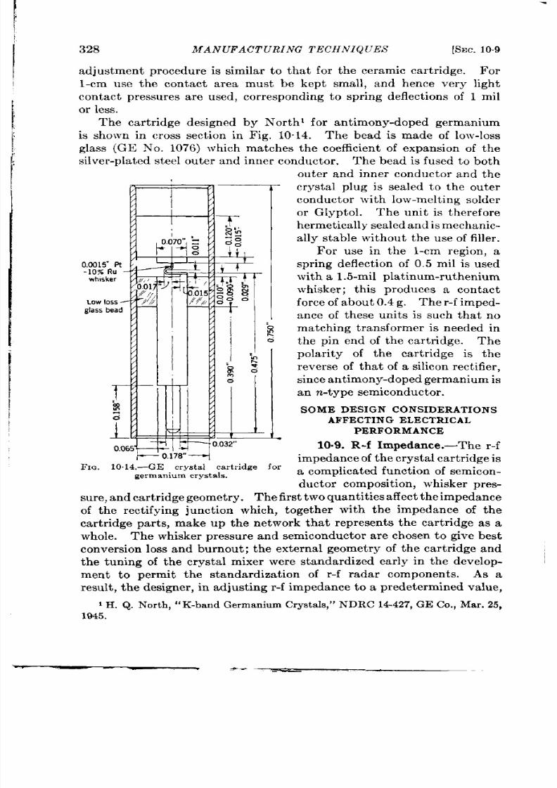
328
MAN UFACTURIN G TECHN IQUES
[SEC.109
adjustmen t procedu re is similar t o tha t for the ceramic ca r t r idge.
For
l-cm use the con ta ct a rea must be kept small, an hence very ligh t
con tact pressu res a re used, cor responding to spr ing de lect ions of 1 mil
or less.
The ca r t r idge designed by Nor th l for an t imony-doped german ium
is shown in cross sect ion in Fig. 10.14. The bead is made of low-loss
glass (GE No. 1076) which matches the coefficien t of expansion of the
silver -pla ted steel ou ter and inner conductor . The bead is fused to both
.
).i78”~
FIG. 1O.14.—GE cr ystal car tr idge for
germa nium crystals.
ou ter and inner conductor and the
con du ct or wit h lo -m elt in g solder
or Glyptol. The unit is th erefore
hermet ica lly s ea led and is mechan ic-
a lly stable withou t th e use of filler .
For use in the l-cm region , a
spr ing deflect ion of 0.5 mil is used
wit h a 1.5-r oil p la t inum-ru then ium
whisker ; th is produces a con ta ct
for ce of about 0.4 g. The r -f imped-
ance of these un its is such tha t no
matching t ransformer is needed in
the pin end of the ca r t r idge. The
pola r ity of the ca r t r idge is the
r ever se of tha t of a silicon rect ifier ,
sin ce a nt imony-doped germanium is
an n -t ype semiconductor .
SOME DESIGN CONSIDERATIONS
AFFECTING ELECTRICAL
PERFORMANCE
1009. R-f Impe ance .-The r-f
im peda nce of t he r yst al ca rt ridge is
a complica ted fu nct ion of sem icon -
du ct or com posit ion , wh isker pr es-
su re, a nd ca rt ridge geomet ry. Th e fir st two qu an tit ies a ffect t he impeda nce
of the re t ifying junct ion which , together with the impedance of the
ca r t r idge par ts, make up the network tha t represen ts the ca r t r idge as a
whole. The whisker press re and semiconductor a re chosen to give best
conv rsion loss and burnou ; the externa l geomet ry of the ca r t r idge and
the uning of the crysta l mixer were standardized ea r ly in the develop-
men t to permit the standardiza t ion of r -f r ada componen ts.
As a
resu lt , t he design er , in adjust in g r-f impe a nce t o a pr edeter min ed va lu e,
1 H. Q. Nor th , “K-band Germanium Crystals,” NDRC 14-427, GE Co., Mar . 25,
1945.
SEC. 10.10]
CONVERS ION LOSS AND BURNOUT
329
has been limited to changes in whisker geometry, interna l geometry of
the car t r idge, and minor hanges in whisker pressure tha t do not appre-
ciably affect loss and burnout . In the case of the ceramic ca r tr idge, a
rect ifier for the 10-cm band with improved burnout and at the same time
good conversion loss when matched at radio frequency can be made by
using bor on-doped silicon and rela t ive y large con tact area .
This un it ,
the 1N28 type, has not been widely used in wart ime radars, however ,
because the r -f mismatch in standard fixed-tuned mixers is too grea t .
The improved burnout obta ined with th is type makes it h ighly desirable
to choose its r -f impedance as a standard for fu ture applicat ions in this
band.
The situat ion in the coaxia l car t r idge is a more for tunate one, in tha t
limited fina l adjustments of r -f impedance can be made by inser t ing a
quar ter -wave t ransformer in the pin end of the car t r idge, either as a
sleeve on t he in ner con du ct or or as a rin g pr essed in to t he ou ter con du ct or .
However , in this case the designer is limited in the t ransformation
obta inable by the space available between inner and outer conductor
and by the frequency ensit ivity in t roduced by the t ransformer . Fur-
thermore, la rge standing waves in the bead, which would in roduce an
appreciable loss, a re to be avoided if possible. In the Radiat ion Labora-
tory coaxia l car t r idge the bead is a half-wave nontransforming elemen t
and the desired r -f impedance is obta ined by choosing the geometry
of the ca r t r idge as shown in Fig. 10.13.
At present wr it ing, the cont r ol
of r -f impedance is a difficu lt problem, one which calls for the utmost
ingenuity and exper ience on the par t of the car t r idge designer .
10.10. Conversion Loss a d Burnout .-The at ta inment of low con-
ver sion loss, as we h ave seen , depen ds on t he n at ur e of t he semicon du ct or
and the contact a ea, the conversion loss for a given semiconductor
and given frequen cy decreasing as the area of conta ct is decreased; on the
other hand we have seen tha t h igher burnout is at ta ined by increasing
the con tact area . Fur thermore, for a given contact the conversion loss
in cr ea ses wit h in cr ea sin g fr equ en cy.
It is a t once evident from these
facts tha t a pract ica l compromise between burnout and sensit ivity must
be ar r ived at in the design of a rect ifier for a given applicat ion . With an
in crease in radio frequen cy the conversion loss, for a given crysta l mate-
r ia l, can be mainta ined only at the expense of burnout , by decreasing
con ta ct a rea .
Impr vement in both burnout and sensit ivity has there-
fore been at tained by improvements in the processing of the semi on-
ductor . 1 As these improvements were made new crysta l types were
specified, which might well be condensed now to, at most , two types for
ea ch fr equ en cy ba nd.
1The specia l ca se of t h e welded -con t act r ect ifier is discu ss ed in Chap. 13.
330
MANUFACTURING TECHNIQUES
[SEC. 10.10
At presen t , ext ensive measuremen ts of r ect ifier proper t ies in the
microwave region have been confined to wavelengths in the regions
a t 25-, 10-, 3-, and l-cm wavelength . On the basis of presen t knowl.
wavelengths will a lso give sa t isfactory per formance a t in t ermedia t e
wavelengths.
I
i
PART III
SPECIAL TYPES


CHAPTER 11
LOW-LEVEL DETECTION
The crysta l r ect ifier has been extensively employed as a low-level
det ect or in t he cr yst al-video r eceiver u sed in con nect ion wit h m icr owa ve
beacons (see Chap. 1). There are many addit iona l applica t ions of
cr yst als a s r ect ifyin g elemen ts a t low power levels in pr obes a nd mon it or s.
Here, we sha ll be ls,rgely con cerned with their use in the receiver , \ vh ich
must have a minimum sensit ivity of abou t 10–8 wa t t for pulses of l-psec
dura tion . This sen sit ivit y has been ach ieved for micr owa ve fr equ en cies
as h igh as 10,000 Me/see.
An a nalysis of low-level det ect ion in volves differ en t pr oper ties fr om
those encoun tered in descr ibing mixer per formance. The fir st par t of
th is discussion i therefore devoted to rect ifica t ion cha racter ist ics of
cryst a ls a t low r-f power levels, and their rela t ion to the physica l param-
eters of the rect ifier . Crysta l-video receiver applica t ion is t rea t ed next
and methods of measur ing the physica l quant it ies of in terest in th is
applica t ion descr ibed. Fina lly, t h ere is an accoun t of he specia l manu-
fa ct ur in g t ech niqu es developed for video cr yst als.
PROPERTIES OF CRYSTAL RECTIFIERS AT LOW LEVELS
11.1. Rect ifica t ion a t Low Levels.—When the rect ifier is used as a
detector , the outpu t termina ls a re connected to a d-c circu it , or , for the
detect ion of r -f pulses, t o the inpu t st age of a video amplifier . Consider ,
for example, a d-c circu it consist ing of a load resistance and a curren t
With r -f po\ ver applied, a small change in the d-c
circu it r esistance causes a small hange in the volt age across the crysta l
and a small change in circu it cur r en t .
The ra t io of the volt age change
to the cu rren t change defines a dynamic ou tpu t r esist an ce for t he cr yst al,
wh ich will be ca lled the “ d-c crysta l impedance, ” or “ video resistance. ”
We have seen in Chap. 2 tha t the d-c impedance for an r -f power input
in the neighborhood of 1 mw is severa l hundred ohms (see Fig. 2.27).
As th e r -f power is lower ed t owa rd th e micr owa tt level, th e d-c impeda nce
r ises to a fixed va lue of sev ra l thousand ohms; th is impedance is just
the reciproca l of the slope of the cu rren t -volt age cha ract er ist ic a t the
opera t ing poin t . In th is r egion of constan t d-c impedance the rect ified
cu rr en t becomes r igor ou sly propor t ion al t o r -f power -th at is, th e cr yst al
is square law in its response. It is in th is square-law region tha t the
r ect ifier op er a tes in cr yst a l-video r eceiver s.
333

(i
;
,.
334
LOW-LEVEL DETECT ION
[SEC. 111
These facts are illust ra ted in Fig. 11.1 from data obta ined by Ber-
inger . 1
In Fig. 11.1 is plot ted on a logar ithmic sca le the short -circu it
cu r ren t and open-circu it voltage a t the ou tput terminals of the rect ifier
as a funct ion of r -f input power for powers up to about one milliwat t .
The varia t ion in d-c impedance is a lso shown. It can be seen tha t the
square-law behavior breaks down as the power is increased above the
~lG.
~o.3
I
I
I
! I
I II
10
r
I
I
xl I
/ “
f
R.f power in watts
11.1.—Rect ifica t ion p roper t ie s of a s ilicon crys t al r ect ifier . The rad io fr eque
3300 Me/see.
m icrowa tt r egion ; t he exa ct p in t a t wh ich th is occu rs va ries fr om crysta l
to crysta l but lies in the range from 2 to 10 ~w.
Because of the possibility of over loading the crysta l it is necessary
to apply correct ions in the use of the crysta l det ector as a monitor of r -f
power.
The cor rect ion clear ly depends on the indica t ing circuit used
with the detector . For example, the open-circu it voltage and short -
circu it cu r ren t show opposite deviat ions from linearity at h igh power
1E. R. Ber in ger , “ Cr yst al Det ect or s a n d t h e Cr yst a l-vid eo Receiver ,” RL Repor t
No. 638, N ov. 16, 1944,
1
SEC. 11.2]
EQUIVALENT-CIRCUIT THEORY
335
level. For th is r eason crysta l probes and monitor s must be ca libra ted
for a pplica tion s beyon d t he squ ar e law r egion .
In the microwa t t r egion the character ist ics of a crysta l rect ifier can
be represen ted by a cur ren t genera tor shunted by a resist ance equal to
the d-c impedance. As the r -f power inpu t is increased, the genera tor
cu r ren t in cr ea ses in pr opor t ion .
As th power l vel is r a ised beyond the
square-law region , the cu rren t increase is more rapid than linear , and the
r esist an ce begin s t o decr ea se.
These two fea tu res a re cha racter ist ic of
crysta l r ect ifier s in genera l, bu t the rela t iv magnitudes of the effect s
va ry from cryst a l to crysta l.
Th e cu rr en t sen sit ivit y is defin ed a s t he r at io of sh or t-cir cu it r ect ified
cu r ren t to absorbed r-f power -tha t is, it is the slope of the cor responding
curve of Fig. 11.1 in the linear region .
This quan t ity, t ogether with the
d-c impedance, is su ficien t to determine the per formance f the crysta l
r ect ifier as a low-level det ect or as we shall see in Sec. 11.5.
In t he 10-cm r egion , t he cu rr en t sen sit ivit y of pr odu ct ion -lin e cr yst als
ranges from 0.5 to 3.0 pamp/pwa t t .
(The cu rve plot ted in Fig. 11.1
is not typica l in th is r espect . ) The d-c impedances show a wide dist r ibu-
t ion of va lu es—fr om 1000 t o 20,000 ohms.
Th e specifica t ion lim it s on d -c
impedance a re g ven for the var ious video-cryst a l t ypes in Appendix D. 1.
In the 3-cm region the cu r ren t sensit ivity ranges from 0.5 to about
1.5 pamp/pwat t , when the best manufactur ing techn iques a re used; d-c
impedances range as high as 30 to 40 kilohms.
Beca use of t he sma ller con t ct a rea , good video crysta ls a re in gen era l
more suscept ible to burnout than mixer crysta ls. Opera t iona l r equ ir e-
men ts, h owever , a re n ot so st r ingent , beca use t he cr yst al-video r eceiver
is not ordina r ily used in applica t ions tha t requ ire a TR switch for pro-
tection.
They must have high enough burnou t , however , not to be
damaged by st r ay radia t ion to which they a re exposed. The burnout
design test s listed in Appendix D for the var ious video-crysta l t ypes a re
an indica t ion of the amount of energy (or power , as the case may be)
t ha t t hey will dissipa te wit hou t a ppr ecia ble impa irmen t.
11.2. E qu iva len t-cir cu it Th eor y. Cu rren t S en sitivity.—An expres-
sion for t he cu rr en t sen sit ivit y, defin ed in Sec. 11”1, in t erms of mea su ra ble
physica l character ist ics of the rect ifying con tact has been der ived by
Ber in ger l and by Lawson, Miller , Schiff, and Steph ens.z Th e pr edict ion s
of the t heory agree only qualita t ively with exper iment ; it has never the-
less pr oved u sefu l in v deo-cr ysta l design an d will u ndou btedly be usefu l
as a basis for a m or e successfu l t heor y as ou r undamenta l u nder sta nding
of t he ph en omen on of r ect ifica tion in cr ea ses.
1L ot. cit .
z A, W. Lawson , P . H . Miller , L. I. Sch iff, a nd W. E . St eph en s, “ Beh a vior of Silicon
Cr yst als a t Low Level P ower s,” NDRC 14-182, U niv. of P en n., Sept . 1, 1943.

336
LOW-LEVEL DETECTION
[SEC, 112
The der iva t ion is based on the equ ivalen t circu it of the crysta l
rect ifier shown in Fig. 2.10. The quant ity R is th e barr ier resista nce
of the rect ifying con tact , wh ich at the low levels considered here is to a
good approximat ion the d-c impedanc of the rect ifier . The term
r is the spreading resistance in the semiconductor , nd C, the barr ier
capacitance.
Th e r ect ifier a t low level will be a ssumed t o be a fou r-t ermin al n et ~~or k
of linear impedances ith the r-f signal applied to one pair of t rminals
and the rect ified ou tpu t appear ing at the other pair as shown in Fig. 11.2.
Because f the low rect ifica t ion efficiency in the square-law region , the
input and ou tpu t terminals a re
,i:~al”m+$:~
effect ively in depen den t of t he loa d-
ing at the opposite termina l pair .
FIG. 11.2.—Networkrep resen ta tionof th e
The on ly connect ion between the
detectorcrystal.
terminal pa irs is the phenomenon
of rect ifica t ion occu rr in g wh en r -f power is absorbed at th e r -f terminals.
It will be assumed fur th r tha t power losses, such as dielect r ic loss s
and skin -effect . loss in the whisker , a re negligible and that the crysta l is
matched to the r -f genera tor . The r-f po er absorbed by the crysta l is
then given by
(1) .
where V is the peak amplitude of the voltage applied to th r -f termina ls
)
and Z is the input impedance of the equ iva len~ circu it of the rect ifier ,
Subst itu t ing Eq. (2) in Eq. (1), we obta in
“!
(3)
The voltage vb across the ba rr ier resistance R is rela t ed to V by the
expression
so tha t
P
v; =
J72
()
(4)
1 + ~ 2 + u2C2r2’
‘w’ +$+”’c’rl”
(5)

SEC. 11.2]
E(j ( ‘I ~“.lLE,I-T .CIRCGIT THEORY
337
To obta in the cur ren t sensit ivity we now need an expression for the
rect ified cu rr en t in terms of
V,).
This expression may be obta ined from
the Taylor expansion of the character ist ic cu rve a t zero bias. [See Eq.
(1.1).] Th e sh or t -circu it rect ified cu rrent is given by
‘i = ; V:f’’(o) — iL
R
(6)
where Y’(O) is the second der iva t ive of the character is ic curve at the
origin.
The second term of the r igh t -hand member of Eq. (6) is included
to take into account the resistance r
in ser ies wit h t he r ect ifyin g con ta ct .
We have seen tha t the d-c impedance is the reciproca l of the slope of the
cha ract er is tic cu rve,
R ‘ j’k’
(7)
so tha t we can write Eq. (6) in the form,
V2
~ = Q ._ l._ f!).
4 (ft + r ) j’(o)
(8)
In Chap. 4 [Eq. (4”27)] w-e der ived the expression for the character -
ist ic cu rve of a r ect ifier :
i = G(e”v — 1), (9)
from which it is seen tha t
.>
~’(o)
~~ = ~.
(lo)
We then obta in from Eqs. (10) and (8)
V’ a
~=fl
4R+r”
(11)
The curren t sensit ivity P is obta ined by dividing Eq. (11) by Eq. (5):
~=;= a , 1 .
( )
(J2C=TR=
2
l+;
+R+r
(12)
The curren t sensit ivity a t zero or very low frequency is obta ined by
set t ing w equal to zero:
(13)
whence
p=po ‘
(14)
u2c ’rR2
l+—
It+r
338
LO~t”-L EVEL DETECT IO.\ -
[SEC.
112
Acheckby Ber in ger on th eva lidit yof Eq. (12) showsonyqualit at ive
agreement bet \ \ -een measured and calculated values of D. Ber inger ’s
resu lts for a good, a medium, and a poor microwave detector crysta l a rc
shown in Fig. 113. Thec rvcss howthec alcula tedvariat ion of ~with
frequency and the poin ts plot t ed are the measured va luesat frequencies
of 600, 3300, and 9300 l~cjsec.
IIeasured va lues of /3 at frequencies of
6.0
4.0
2.0
0.1
.008
.006
2
4 68103 2
4 68104 2
FrequencyIn Me/see
FIG. 11.3.—T-ar ia t ion of cur ren t sensit i~.ity with frequency, The poin ts
values; the cm yes :,, e mlcula t rd f, on > Eq. (12).
art?
measured
2 kc/see, 1 J Ic/see, and 10 31c/scc \ vere identical and served to give the
value of PO. The values of R, r , and C for the three crystals are given in
Table 11.1.
‘rABLE 111.-(7ONTACT P.4RAMETEFWOF THE ‘rHREE (’RYST.41S ~sEl) Fon I;IG. ]1.3
Crysta l XO. R, ohms r , ohms
(’, jlp f
45,5 0.75
KH 1290
1770
27.6 0,58
KD 7053
1700
40.2
0.25
The d-c impeda ce R was m asured by the method descr ibed in
Sec. 11.9. The barr ier capacity C was measured at 10 lIc/sec wi h a
twin-T circuit similar to tha t used in the Genera l Radio 821-.4 Bridge. 1
Th e exper im en ta l pr ocedu re in volved a mea su remen t of over -a ll ca rt ridge
capacity and an auxiliary measurement of the residual capacity when
the whisker has been backed off from the contact . At zero d-c bias tkc
bar rier ca pa city is ver y n ea rly t he differ en ce between t hese t wo r ea din gs.
The spreading resistance r was measured by biasing the crysta l to a volt
or so in th e posit ive direct ion (t o t h linea r por tion of th e ch ara cter ist ic)
and mea sur in g t he clifferen tia l resist ance at th at point with an a -c sou rer .
1 D. B.
Sinciair,
‘(Th e Twin T—A New Type of A“ull Inst rument for h~eas(i]il ~
Imped an ce a t F requ en cies u p t o 30 Lfega cycles, ” P ,O,. I. R . E ., 28 (~0, 7), 310 (1940).

SEC. 112]
EQUI VALEAJ T-CIRCUIT THEORY 339
Figure 11.3 shows tha t both the ca lcula ted and measured values of ~
decrease with increasing frequency, but tha t the former decrease more
rapidly. This discrepancy may be due to a decrease in the effective
bar r ier capacity at micr owave fr equ en cies fr om it s low-fr equ en cy va lu e.
Su ch an effect wou ld be expect ed if t he t im e r equ ir ed to ion ize t h e dona tor
levels in the semiconductor were long compared with the per iod of the
applied voltage. This theory has been discussed in Chap. 4 for the case
of h igh -level r ect ifica tion , bu t qu an tit at ive r esu lt s for t he low-level
case
have not yet been wor ked out .
At zero d-c b as,
R>> r, so tha t Eq. (12) r educes to the approximate
relation
1
p = ; i-+ .’Cm’
(15)
It is evident from Eq. (15) tha t o can be increased by increasing a and
decr ea sin g C,
r,
and
R. IXow C is propor t iona l to the area of contact ; R
is inversely propor t iona l to the area of con tact , and r is inversely pro-
portional to the r adiu s of con ta ct .
Th e pr odu ct
G’zR r is
t h er efor e pr o-
portional to t he radius of contact .
The value of P can therefore be
improved by decreasing con tact a rea through the use of li h t con tact
pressures.
There a re two limitations on how far one can go in th is direc-
t ion . The fir st limitat ion is mechanica l stability. Both the d-c resist -
.
an te and the curren t sensit ivity a re very sensit ive to slight changes in
con ta ct pr essu re, a nd wit h ligh t pr essu res mech an ica l st abilit y is difficu lt
to achieve.
On this score the coaxia l car t r idge design appears
to
be
defin it ely su per ior t o t he cer am ic on e.
Th e secon d limita t ion is an u pper
limit on R which arises from considera t ion s of r eceiver design .1 F ur th er
improvemen can be achieved if C can be decreased by some means other
than decreasing the con tact area , but must await fu r ther resea rch on the
physics of th e barr ier la yer .
We have seen in Chap. 4 tha t exper imenta l va lues of a a re a lways less
th n the theoret ica l va lue of 40 volt s.–l. It was fur ther poin ted ou t
there tha t this discrep ncy may be ascr ibed to fluctua t ions in barr ier
space cha rge or contaminat ion of the con tact sur faces producing loca l
fluctua t ions in the work funct ion over the con tact a rea .
Th e va lidit y
of the linear rela t ion between B and a, predicted by Eq. (15), has been
invest iga ted by h’leyerhof and Stephens.z They measured a and P for a
group of good video crysta ls designed for the 3-cm band. The values of P
to
13 volt s–i. This discrepancy did not appear to be explicable in t erms of
differences in capacity and resistance of the crysta ls. Whether it is due
1See Radar Beacons, Vol. 3, Radia t ion Labor a tor y Ser ies .
s W. E. Meyer hof a nd W. E. Steph en s, “X-ba nd Video Cr ysta ls, ” N-D C 14-274,
Un iv. of P en n,, h fa y 20, 1944.

340
LOW-LEVEL DETECTIO,V
[SEC. 11.3
to an inadequate model for the equiva len t circuit or to the difficu lty in
obta ining good quant i a t ive da ta on crysta l parameters is open to quest ion.
Improvements in cur rent sensit ivity to da te have been achieved
la rgely by decreasing contact pressure, by an ernph-ica l study of doping
and sur face t rea tment of the semiconductor , and by adjust ing the contact
for opt imum video per formance.
11s3. Effect of Bias on Low-level Proper t ies. D-c Impedanc .—As
we have seen , the d-c, or video, impedance is just the reciproca l of the
slope of the character ist ic cu rve a t the opera t ing poin t .
With zero d-c
bias the va ues range from about 2000 to 40,000 ohms for silicon crysta ls
and are of the order of 106 ohms for germanium welded-con tact crysta ls.
At a orward bias of about 0.2 or 0.3 volt the values a re reduced to the
n eigh bor hood of 100 ohms for silicon a nd 104 ohms for germ an ium.
The
L
1-
R
1
r
c’
, • f!
FIG, 11.4.—Equivalen t circu it of a
r ect ifier ca rt ridge u sed for det ermin in g
barrier
capacitance. L—whisker in -
ductance: R—ba r ier resistance; C—
barr ier capacitance; r—spreading re-
sist an ce; C’—r esidu al ca pa cit an ce of t he
cartridge.
la t ter is a useful vayue in the crysta l-
video receiver applicat ion , but a for -
ward bias of more than about a tenth
of a volt in the case of the silicon
crysta l r educes the lower limit of the
video impedance range below a use-
fu l va lue.
Capacitance.-1t was
poin ted out
in Chap. 4 tha t , in genera l, t~vo
methods have been used to measure
the barr ier capacitance. One of these
is t e dir ect measurement of the
impedance of the rect ifier with a
suitable impedance br idge at a low frequency ( = 10 31c/see). This
method has been used by Ber inger , as out li ed in the preceding sect ion ,
and by the Pennsylvania Crysta l Group.’
The model of the rect ifier assumed by Lawson e~ al. is shown in
Fig. 11.4. This model differs from that previously used only in the
addit ion of the whisker inductance
L
and the residual capacitance of
t he ca rt ridge C“.
The la t ter is the capacitance of the car t r idge with the
whisker just r emoved from the crysta l and is approximate ely constan t
from car t r idge to car t r idge, having a value in the neighborhood of 0.35
ypf. The whisker inductan ce
L is
determined by a measurement of the
impedance of a car t r idge in which the crysta l is replaced by a piece of
meta l of ,similar geometry. It has a value in the neighborhood of
0.01 gh . The r esis tances
R
and
T
a re determined by an anaiysis of the
d-c character ist ic cu rve. Having determined these constan ts, one can
ca lcu la te t he ca pa cit an ce C fr om t he mea su red impeda nce of t he ca rt ridge.
1A. W. Lawson , P . H. h filler , L. I. Sch iff, a nd W. E. St ephens, “Ba rr ier Ca pacity
in S ilicon Car t r idge Rect ifier s ,” NDRC 14-140, Univ. of P en n., h la y 1, 1943.

i.
SEC. 11.3]
EFFECT OF BIAS ON LOW-LEVEL PROPERTIES
341
Measurements were made by the Pennsylvania group on silic n crys-
tals with a Genera l Radio 916A Bridge, which measures ser ies resistance
and reactance, and with a modified twin-T br idge, which measures shunt
conductance and susceptance. With the Genera l Radio br idge a resist -
ance of about 150 ohms is connected in pa ra llel across the ca r t r idge to
br ing the impedance within the range of the instrument . With both
br idges the applied emf must be as small as possible because of the non-
linear ity y of the bar r ier resistance. A compar ison of results obta ined with
the two br idges show sat isfactory agreement with zero d-c bias applied
to the crysta l. With a posit ive d-c bias, however , there is a discrepancy
not yet expla ined in the two values. The observa t ions by the br idge
method show that the capacity r ises r pidly with forward bias to a
va lue which may be, at a bias of 0.5 volt , as much as 100 t imes its va lue
at zero bias. It is est imated, however , tha t the er ror at this bias may
be as la rge as a factor of 10.
Th s er ror ar ises from the fact tha t , as the
posit ive bias is increased, the voltage across the ba r r ier decreases, and
most of the applied voltage is across the spreading resistance.
Therefore
a small er ror in determining the spreading resistance in t roduces a la rge
er ror in the va lues obta ined for the capacitance. Because of this and
the discrepancy between values obta ined with the two types of br idge,
the result s of the br idge measurements can at best be considered qua li-
ta t ively t rue. With small va lues of nega t ive bias, up to about – 0.5 volt ,
the br idge measurements show a small decrease in capacitance, followed
by an increa se which , at a bias of – 2.5 volts, may be as a rge as ten t imes
the va lue at zero bias.
The second method of determining capacitance makes use of Eq. (14)
of the preceding sect ion. In the use of this equat ion we must assume
tha t the discrepancy between the measured va lues of L?and the va lues
ca lcu la ted using the low-fr equency va lue of capacitance is brought about
by the var ia t ion of capacitance with fr eq ency discussed in the previous
sect ion . One then obta ins the r -f capacitance in terms of measured
values of @ at low and at microwave frequencies nd the quant it ies R and
r . Meyerh of, Ser in , an Vough t, 1using th is meth od, made measurements
on silicon a nd germa nium r ect ifier s.
With silicon crysta ls a t a posit ive
bias of 0.2 volt , the r -f capacitance increases to not more than twice it s
va lue a t zero bias. With germanium crysta ls the effect is grea ter ; a t a
forward bias of 0.4 volt the capacitance is about 10 t imes as grea t as a t
zero bias. Like the br idge method, th is one is inheren t ly i accura te
because of large er ror s in the calcula ted va lues in t roduced by er ror s in
mea su rin g t he cr yst al pa ramet er s.
I W. E. 31eycrhof, B. %-in , and R. H. Vought , “X-band Crysta l Per formance
with Bias, ” IiDRC 14-505, Un iv. of P en n., J u ly 6, 1945.

342
LOW-LEVEL DETECTION
Current Sens-it ivitv.—The effect of forward bia s
—
;!
[SEC. 114
on cu rr en t sen sit ivit y
has een invest iga ted by Meyerhof, Ser in , and Vough ’ for type 1X3~
silicon rect ifiers a d for the germanium welded-contact rect ifiers at a
r adio fr equency of 10,000 Me/s ee.
Typica l r esu lt s a re sh own in F ig. 11.5.
The current sensit ivity r ises to a maximum at 0.1 to 0.2 volts for s licon
and 0.3 to 0.4 volts for germanium.
The maximum for silicon has
value severa l t imes tha t a t zero bias; the curren t sensit ivity for ger -
manium rises from a very small value to a value a t the maximum com-
parable to the maximum value for silicon . The rapid init ia l r ise for
o
0.1 0.2 0.3 0.4 0.5
Forward bias in volts
FIG. 11 .5.—Curren t sensit vity as a
funct ion of forwa rd bias for a silicon
a nd a welded-con ta ct ger ma nium cr ysta l.
germanium may be at t r ibuted to the
rapid decrease in
R,
which at zero
bias has a value of th order of 10s
ohms. It is clear t a t the current
sensit ivity becomes zero when the
forward d-c bias voltage is grea ter
tha n t he con ta ct differ en ce of pot en -
t ia l; in t his ca se t he ba rr ier r esist an ce
and a become zero and the opera t ing
point is on the linear part of the d-c
characteristic.
11.4. Var ia t ion of Low-1evel
Proper t ies with Tempera ture.—A
va r ia t ion of R and P wit h t emper a tu r e
is to be expected on theoret ica l
grounds. We have seen in Chap. 4 [Eq. (4.33)] tha t the theoret ica l
expression fcr t !le curren t density through the barr ier is
.+, ev
—-—
i = A’e ‘~(em – 1), (16)
where A! k a constan depending on the conduct ivity of the se icon-
ductor, @O k t h e effect ive con t act pot en t ia l d iffer ence, V k t h e pot en t ia l
applied to th e barr ier , and T is the absolu te tempera ture.
The low-level
resistance is the re iproca l of the deriva t ive of i with respect to V. With
no d-c bias (V = O) th is is
~ = g ee+o,k=
eA’ “
(17)
Over the tempera ture range of in terest in video-crysta l applicat ions
( –50° to +70°C), we see that Eq. (17) predi t s an approximately
expon en tia l in cr ea se in
R as 1’ decreases.
F igure 11.6 shows a typical
plot of observed values, obta ined by the University of Pennsylvania
1 L ot. m “t

1
{
I
I
{
I
SEC. 11.4] VARIATION OF PROPERTIES WITH TEMPERA 1’URE
343
group;1 R/T is plot ted on a logar ithmic sca le as a funct ion of l/T for an
unfilled silicon video crysta l over the tempera tu re range from about
–30”C to +70”C. Th expected linear behavior is clear ly confirmed
The main effect of tempera tu re on curren t sensit ivity is probably
caused by the change of R with tempera ture [see Eq. (15)] Figure 11.7
sh ows t he t heor et ica l va ria tion in R and in P as a funct ion of t empera tu re
60
40
/
/
20
<
10
/ ~
8
/
6
/’
4 i 0
.
2-
3.0 3.2 3,4 3.6 3.8 4,0 4,2x10-’
l/ T m (°K)-l
FIG. 11 . 6.—Va r ia t ion of vid eo r es is ta n ce
wit h t emper at ur e for a silicon cr yst al.
25
220
c
0
m
Video resistance
% 15
10
J
5.0
3
4.0 ~
3.0 “;
.=
.=
2.0 ‘g
w
1.0 5
5
v
n
al -20 0 +20 +40 +a +80-
Temperature in°C
FIG. 11 .7.—Th eor et ica l va ria tion of video
resistance and
cu rr en t sen sit ivit y
with
Emt e m
40 -20
0 +20 +40 +60 +S0
-40 -20
5
0 +20 +40 +60 +60
Temperaturen “C
v
Temperature m “C
FIC. 11.8.—Effect of tempera ture cY-
FIG. 11 9.-Effect of tempera ture cy-
clin g on video resistance for an unimpreg-
cling on cur r en t sensit ivity for an unim-
na ted s ilicon ca r t rid ge .
p regna t ed s ilicon ca r t r dge.
for a crysta l having a video resistance of about 6000 ohms at room tem-
pera ture. In genera l the observed values of 6 r ise with increasing tem-
pera tu re a lthough there are cases where the observed ~ falls off at h igher
t em per at ur es, in disa gr eem en t with t he t heor y.
Figures 11.8 and 11.9 show observed values of R and /3 taken around
a cycle from — 40”C to +70°C by Smith et al.2 These data are for an
I A. H. Smith, B. Ser in, W. E. Meyerhof, and W. E. Stephens, “Tempera ture
Var ia t ion of Low Leve l Crys ta l Per formance ,”
NDRC 14-308, Un iv. of P en n., Au g. 17,
1944.
2Lot . cd .

344
LOW-LEVEL DETECTION
t r efilled cryst a l r ect ifier a t a r adio frequency of
crysta l holder was fixed-tuned to match a t room
II
[SEC. 11.5
10,000 Me/see. The
tempera tu re] and the
available r -f power was held const an t dur ing the exper imen t .
Th e
tempera tu re var ia t ion was obta ined by enclosing the crysta l holder in a
thermally insu la ted box which held either hot wa ter or dry i e in a lcohol.
The tempera tu re was measured by means of a thermocouple. A temper -
a tu re cycle requ ired severa l hour s to run for a maximum ra te of change
of t emper at ur e of about 2°C/min .
In genera l, filled ca rt ridges sh ow a hysteresis effect t ha t in some ca ses
is pronounced at low tempera tu res. Also ome cryst a ls a re found to be
er ra t ic in per formance. These either do not retu rn to the or igina l va lues
a fter t empera tu re cycling, or the repet it ion of the cycle does not r epro-
duce the fir st cu rves. The hysteresis effect is probably la rgely a t t r ibu t -
able to a thermal lag in the filler ma ter ia l, because the effect is much
smaller in unfilled crysta ls. The er ra t ic effect s a lso appea r to be la rgely
due to the filler . T e differen t ia l expansion of the ca r t r idge par t s has
been measured by the Pennsylvan ia group and does not appea r t o be
la rge enough to change the spr ing deflect ion more than 0.2 mil for 100”C
tempera tu re change. The effect of t empera tu re hanges of the filler
may be a distu rbance of the adjustmen t (the pressu re is small for good
video crysta ls) either by nonisot ropic expansion of the filler or by a
viscou s lon git udin al for ce exer ted by t he fill r on t he wh isker .
Whatever
the cause, the er ra t i effects a re m st pronounced below room tempera -
tu re. The tempera tu re-cycling test s ou t lined in the J AN specifica t ions
a re su fficien t t o in su re fa ir ly st able video u nits bu t do n ot a ppea r su fficien t
to insu re tha t the crysta l opera t e in a stable fash ion at t empera tu res much
below O“C. We must r emember tha t even in the absence of er r a t ic or
h yst er esis effect s, t her e exist t he va ria tion s of R a nd (3wit h t emper at ur e
which appea r to be inheren t in the rect ifying con tact .
THEORY OF LOW-LEVEL DETECTION
As with frequency conversion , w are concerned, in low level detec-
t ion , with the conversion of microwave power and with the genera t ion of
noise by the crystal and amplifier .
In the f ollowing analysis, in t roduced
by Ber inge ,l an expression will be der ived for the ou tpu t signa l-t o-noise
voltage ra t io of a crysta l-video receiver .
The analysis enables us to
define a quant ity ca lled the “figu re of mer it ,“ wh ich expresses quant ita-
t ively the excellence of the video-cryst a l det ector in terms of cur ren t
sensit ivity and video resistance.
11.6. The Figure of Mer it of a Video Crysta l.-The video crysta l of a
crysta l-video receiver is moun ted in a crystal holder pro ided with r -f
I E ). R, Ber inger , Crysta l Detectors and the Crysta l-video Receiver , ” RL Repor t
No. 638, Nov. 16, 1944.
—

1
J
I
(
I
/
I
I
I
I
\
I
L
SEC.
115]
THE FIGURE OF MERIT OF .1 l“IDEO CR YS TAL
345
t ermina!s (a coaxia l line or wavegu ide) in to \ rh ich r -f po\ ver is coupled,
and video terminals from which th outpu t video signal is obta ined.
The cryst a l det ector and video input circu it of the video amplifier may be
represen ted by the cir cu it of Fig. 11.10. The rysta l is r epresen ted by a
cur ren t genera tor shun ted by the video resistance Ii of the crysta l, t he
cu r ren t being a linear funct ion of the r -f power absorbed by the cryst a l.
The quant ity C is the combined capacity of the choke syst em of the
cryst a l holder and the fir st amplifier
tube.
,18, w
The rect ified cu r ren t i is given by
i = (3P,
FIG. 11 .10.—Equivalent input c rcu it
where @ is the cu rren t sensit ivity and
of the crystal -v]deo receiver.
P
k the absorbed r -f power . Disregarding the effect of G on t ransien t
signals, one obta ins for t he signa l volt age e on the gr id
he ou tput signa l volt age from the amplifier is then
E = 13PRG, (20)
where G is the volt age gain of the amplifier .
The outpu t noise of the receiver or igina tes in both the crysta l and
the receiver . In the absence of feedback and t ransit -t ime effect s, the
r eceiver noise cont r ibu t ion is oft en represen ted by an equiva len t noise-
genera t ing res is t ance
RA
in ser ies with the gr id cir cu it of the input st age;
th is r sistance does not load the circu it bu t genera tes a mean-squa re
noise volt age of 4kTBRA. The magnitude of R. can be deduced from
theory; for a high-mu pen tode such as the 6AC7, it is about 800 ohms.
It can a lso be measu red by a simple procedure, which consist s in placing
va r ious res is tor s Rx between the m-id and ca thode of the fir st tube and
observing the ou tput noise power .
The ou tput noise power is propor -
t iona l t o RA + Rx. For some par t icu lar va lue of Rx the outpu t noise
power is just double tha t with the gr id connected direct ly to the ca tho e;
this resist an ce is t hen numer ica lly equal t o RA. Va lu es of RA of 1000 to
1200 ohms have been obta ined by Ber inger l for a typica l video amplifier
emplo ing a 6AC7 tube in the fir st st age.
In th is measuremen t noise
component s from the en t ir e pass band of the amplifier con t r ibu te to the
ou tput noise power , inclu din g microphonics and flicker noise in t he low-
fr equ en cy r an ge; con sequ en tly R. will be somewha t h igher than the
theoret ica l shot -effect va lue. In the J AN vide -cryst a l specifica t ions a
va lue of 1200 ohms has been chosen for
RA.
L13. R. Ber inger , ‘‘@-sta l Detectors and the crysta l-video Receiver , ” RL Report
No. 638, Nov. 16, 1944.

#
DETECTION
nois e gener a t ed
[SEC. 11.5
by a crystal in the
346 LO I1’-LEVEL
In the absence of d-c bias the
microwa t t r ange of r -f power is a lmost en t ir ely the J ohnso noise of a
r es is tance equa l to the d-c im eda nce of t he cr yst al.
The tot a l ou tpu t
rms noise volt age ~ of the crysta l-video receiver , with nod-c bias, is then
given by
N = G ~4kTB(li? + R .),
(21)
where G is the volt age gain of the receiver , and B, t he effect ive n oise
bandwidth , is defined as n Eq. (2.14).
Th e ou tpu t signa l-to-n oise volt age ra tio of t he r eceiver is obta in ed by
combining Eqs. (20) and (21):
E /3PR
N = d4kTB(R + R.)-
(2’2)
Equat ion (22) may be writ t en in the form
The quant ity M, which conta ns all t he crys a l pa rameters appea r ing in
Eq. (23), is a cr it er ion of excellence of the video crysta l, since a ll good
Pulsed
signal
Synchr@
generator
15 db of
scope
Iossycable
~
FIG. 11.11 .—Block diagra m of appa ra tu s for mea su rin g t he sen sit ivity of a cr yst al-video
receiver.
video amplifiers have essen t ia lly the same value of RA.
The term M is
ca lled the “figu re of mer it ” of the video crysta l.
The sensit ivity of a crysta l-video receiver has been computed by
Ber in ger by means of Eq. (23) and compared with tha t measured direct ly
by the applica t ion of pu lsed r -f signa ls of frequency 3300 Me/see to the
receiver.
A block diagram of the appara tus is shown in Fig. 11 ~11. Th e pu lsed
sign al gen er at or is of t he ‘‘ off-pu lsin g” t ype: it is pu lsed ou t of oscillation
for 1 ~sec a t a repet it ion fr equency of 1 kc/see. This type of signa l
genera tor is advan tageous for pr cision work , since the pulse power is
ver y n ea rly equ al to the a ver age power m ea su red wit h a bolometer.
Th e
receiver had an in t egra t ed bandwidth of 3 Me/see.
The resu ts of t e ca lcu la t ion and measuremen ts for severa l cryst ls
a re shown in Table 11.2. The first colu n gives the figu re of mer it
of the cryst a l. Column 2 lists the absorbed r-f pulse power ca lcu la ted by
i
-r
I
I
I
1
,i
SEC. 116]
EFFECT OF D-C BIAS ON FIGURE OF MERIT
347
means of Eq. (23) for E/~ 1. Column 3 gives the pulse power or
“minimum detectable signal’ ‘—that is, the smallest immediately seen
on an A-scope when its posit ion a long the t race is unknown.
Column 4
iists the puise power for the
“tangent ia l signa l’ ‘—tha t i , the signal
which raises the noise by its own width . Both the minimum detectable
signal and the tangent ia l signai a re somewhat vague in an absolu te sense;
the ia t ter is of some pract ica i importance, for i is this signai which is
commoniy regarded as necessary to t r igger an elect ron ic switch with a
negligible n umber of spurious even ts fr om noise fluct ua tions. It a ppear s
that the minimum detectable signal is about tha t for which the signal
voltage is equai t o the rms noise voltage.
TABLE11.2.—ACOMFARISONFCALCULATEDNDillEASUREDALUESOFCEYSTAL-
VIDEORECEIVERENSITIVITY
Figure Calcu lated P
Min imum det ect -
Tangential
of mer it for E/ ~ = 1, watts able signal, wat t s signal, wa t ts
110 2.0 x 10-’
2.0 x 10-’
5.3 x 10-’
59 3.7
3.7 11.0
115 1.9 2.9
5.0
50
4.4 3.0 10.0
95 2,3
2.6
6.2
11.6. Effect of D-c Bias on Figure of Mer it .—The conver ted noise
from d-c bias was seen in Chap. 6 to be very ia rge in the video f requency
range.
For th is reason , the analysis of the preceding sect ion , in wh ich
only J ohnson noise was assumed in th detector , is not va lid when d-c
bias is used. Instead, one in t roduces the video noise tempera tu re of the
crysta i in to the expression for the figur e of mer it [Eq. (24)], wh ich now
becomes
M= ‘R
~Rt •i- R.’
(25)
where t is the noise tempera ture of the biased crysta i for a iven video
amplifier . Since the noise output var ies inversely with the video fre-
qu en cy, t wiil in cr ea se r apidly a s t he iow-fr equ en t y cu toff of t he amplifier
is decreased and is therefore a funct ion of the amplifier pass band. As
t he posit ive bia s is in cr ea sed fr om zer o, R decreases rapid ly, j3goes through
a maximum, and t increases.
The net effect on M h as been in vest iga ted exper im en ta lly by Meyer -
hof, Ser in , and Vought ,’ using appara tus similar to that shown in Fig.
11.11. The input and biasing circu it s a re shown in Fig. 1112. The
output of the signal genera tor consisted of 2-psec pulses at a repet it ion
frequency of 800 pps, and radio frequency of 10,000 Me/see. The pass
1 La . cit.

348
LOW-LEVEL DETECTION
band of the video amplifier was from about 20
,{
[SEC, 11.7
kc/see to 2.8 Me/see
Two methods wer e used t o obta in the figu re of mer it . In the fir st
method, the signa l level was decreased unt il t he signa l was just equal to
)
noise; the r -f power level was then not ed.
be ca lcu la ted by means of Eq. (23). I t he second method, the signa l
.
FIG.. 11.12.—Input and biasing circu it used for measur ing video-crysta l r eceiver
performance.
d eflect ion a nd “a ver a ge”
n oise deflect ion wer e observed for a sta ndar d
r -f power input . The two methods cor rela t ed on the average with an
average difference of about 10 per cen t . Typica l r esu lt s for a welded-
con tact germanium crysta l and a 1N31 silicon unit a r e shown in Fig.
11.13, in which the figure of mer it is plot ted as a funct ion of bias. The
in it ia l r ise in M for a welded-con ta ct unit is pr oba bly la rgely a ccou nt ed
o
0.1 0.2 0.3
0.4 0.5
Forwardias in volts
FIG. 11 .13.—Figure of merit as a
funct ion of d-c bias: Avl N31 silicon
r ect ifier ; B—weld ed -con t act german ium
rectifier.
for by the la rge init ia l increase in d
(see Fig. 11.5).
The figu re of mer it
a t the opt imum bias is comparable to
that for silicon video crys als. As
indica ted in the figure, t he opt imum
bias is from 0.2 to 0.3 volt for t he
german ium welded-con tact un it , and
zer o for silicon .
11.7. The Effect of Tempera ture
Var iat ion on Crysta l-video Receiver
Per formance.-The var ia t ion of the
figure of merit with tempera tu re
ar ises from the variat ion of video
r esist an ce a nd cu rr en t sen sit ivit y dis-
cussed in Sec. 11.14. As the tem-
per at ur e is decr ea sed, (3 d ecr ea ses a nd
I? increases, so tha t the two effect s
t end to cancel each other so fa r as the figure of mer it is concerned.
Figu re 11.14 shows the va r ia t ion of the figu re of mer it ov r a
tempera tu re cycle from
– 40° to + 70”C for the same crysta l with
which the da ta of Figs. 11.8 and 11.9 wer e t aken .
Th e figu re of mer it
may also
increase with
lit tle ch an ge.
increasing tempera ture, or it may exper ience

SEC. 11.7] EFFECT OF TEMPERATURE O,V PERFORMANCE
349
The var iat ion in receiver per formance caused by changes in crysta l
tempera ture is undesirable in beacon applicat ions. The var ia t ions of
input signal voltage and input rms noise voltage with tempera ture has
been calcula ted by Smith et al., 1 for a typica l crysta l with a figure of
mer it of 60, a video resistance of 10,000 ohms at room tempera tu re, and
t ypica l va ria tion s of R and Q with tempera ture. The input signal voltage
e is just the product
@PR
an d was ca lcu la ted for an r -f power of 10–s wa tt .
The rms noise voltage fi was ca lcula ted by means of Eq. (21) by the
relation
iv
~=—.
G
(26)
The results of the ca lcula t ions are shown in Table 11.3 for tempera tures
of —40°, +27°, and +70”C. The first two columns of the table list
the values of R and @used in the ca lcula t ions. It can be seen tha t the
signal voltage at 70°C is approxi-
mately the same as the noise volt -
age a t —40”C. This means tha t ,
if the receiver is set to actua te an
elect ronic t r igger ing circuit for a
signal of 10–8 wat t a t h igh temper-
a ture, it may actua te it from noise
a t low t emper at ur es.
It is advis-
able, th refore, to con t rol the am-
Im
40 -20 0 +20 +40 +60 +80
Temperature in ‘C -- ‘-
FrG. 11.14.—Effect of tempera ture
cycling on the figure of mer it of an unim-
bient tempera ture a t which the
pr egna tedsiliconcryst alrectifier.
video crysta l opera tes so that it does not go below about O°C in non-
adjustable insta llat ions where the set is requ ired to opera e over a wide
r ange of t emper a tu r es .
‘TABLE 11.3.—EFFEcT OF TEMPERATURE VARIATION ON CRYSTAL-VIDEO RECEIVER
PERFORMANCE FOR A YPICAL VIDEO CRYSTAL
Tempera-
R,
t u re, “C ohms
– 40 40-00
+27 10400
+70
5-000
b,
#rL//.lw
0.3
0.6
0.7
n, e,
pv
pv
34 120
19
00
15
35
e/ii
3.5
3,1
2.3
MEASUREMENTS
We have seen tha t the performance of a crysta l-video receiver can be
expressed quantita t ively in terms of the figu re of mer it , which in turn
is a funct ion of curr ent sensit ivity and video res stance.
The following
I A. H . Sm it h, B. Ser in ,W. E . Tvleyer hof,and W. E . S tephen s, “Temper a+.i,u
:,
Variat ionof LowLevelCrystal Performan ce,”
NDRC 14-308,Univ. of Penn.,Aug. 17
1944.

350
LOW-LE EL DETECTION
[SEC.
11.8
sect ions a re devoted to a descr ipt ion of the equ ipmen t and methods
developed at t he Radia t ion Labora tory by Ber inger ’ for the measu rement
of these quant it ies. The equipmen t is adapt ed to both labora tory and
pr odu ct ion t est in g.
11.8. R-f Equ ipment and Measurement s.—To reduce reflect ion
losses to a min imum the crysta l should be matched to the r -f sou rce. In
a crysta l-vid o receiver the ant enna is usua lly matched to the r -f line
wh ich , in tu rn , is connect ed to the crystal holder ; the crysta l holder then
employs matching t ransformers which match it to the line.
In test
equipmen t an r -f signal gen er at or is con nect ed t o t he line by an a tten ua tor
which can be adjusted to provide r -f power to the line at a power level
of a few microwa tt .
R-j Equ ipm en t jor he 10-cm Band. -h’early all the measurements in
the 10-cm band have been made at an r-f wavelength of 9.1 cm, in
accordance with the JAN specifica t ions for test ing in this band. A
klyst ron connected to the crysta l holder with about 20 db of lossy cable
is a suitable signal genera tor . The crysta l is matched to the coaxia l line
from t he signal gen er at or by in cor por at in g in to t he cr yst al h older suitable
transformers, such as paralle stubs and quar ter -wave lines in ser ies.
These may be either tunable or fixed-tuned.
Like mixer crystals, video crystals have a dist r ibut ion in r -f imped-
ance. This dist r ibut ion is such that for the 1N27 type an approximate
match can be obta ined by means of a single tuning stub. Such a crysta l
holder is specified in the J AN speci ica t ions. It is shown in cross sect ion
in Fig. 11.15. The stub is tuned for maximum rect ified curren t by means
of a sliding shor t -circu it ing plug which makes spring-finger con tact
\ r ith the inner and out er con du ctors.
The pin of the car t r idge fits into
spring fingers on the cen ter conductor , and the head of the car t r idge is
h eld by a copolyst yr en e wa sh er .
The video or d-c connect ions a re made
through an r-f choke which makes spr ing con tact with the head of the
cartridge.
Recent ly a fixed-tuned holder has been designed by Ber inger to
r epla ce t he on e ju st descr ibed.
A cross sect ion of this holder is shown in
Fig. 11.16. The crysta l ca rt r idge is held by spring fingers at both the
head and pin . The ca r tr idge is much easier to insert and remove than
in the preceding design , a fea ture of impor tance in product ion test ing.
The stub is shor t -circu ited for r-f power by the quar ter -wave choke
mounted on the cen ter cond ctor of the stub; the video connect ion to the
crysta l is made through the cen ter conductor .
The center -conductor
assembly is insulated by means of the copolystyrene nut on the stub
1E . R. Ber in ger , “Cr yst al Det ect or s a nd t he Cr yst al-video Receiver ,” RL Repor t
X-o, 638, X“ov. 16, 19 4; “Oper a t in g I ns tr u ct ion s for t h e Radia t ion Labor a t or y X-band
Cr yst al Det ect or Test Set ,” In ter na l Gr ou p Repor t 61, Au g. 10, 1944.

I
I
I
SEC. 11.8]
RF EQUIPMENT AND MEASUREMENTS
351
and the copolystyrene sleeve and be ds near the r-f input terminals.
The sleeve on the center conductor provides essent ia lly an open ircuit
for video and d-c fr equencies and a negligible impedance for r -f fr equencies.
FIG.
11. 15.—Tunable crysta l holder for video-crysta l test ing at a wavelength of 9.1 cm.
The tuning is fixed at the cen ter of the r -f impedance distr ibut ion.
The center is determined by a measurement of the r -f impedance dist r i-
Video ttrminals
A
FIG. 11
k
Copolymerstyrene
nut
NH
%rin~ fingers
R.f
terminal
I Cr stal cartridges ~
‘Copolymerstyrene -
insulators
.16.—F ixed-t un ed cr yst al h older for video-cr yst al t est in g a t a a velen gt h
of 9.1 cm.
but ion of a representa t ive sample of rect ifier units. Such measurements
are made with a standing-wave detector which is inser ted between the
at tm”uator and crysta l, the method being similar to tha t descr ibed in
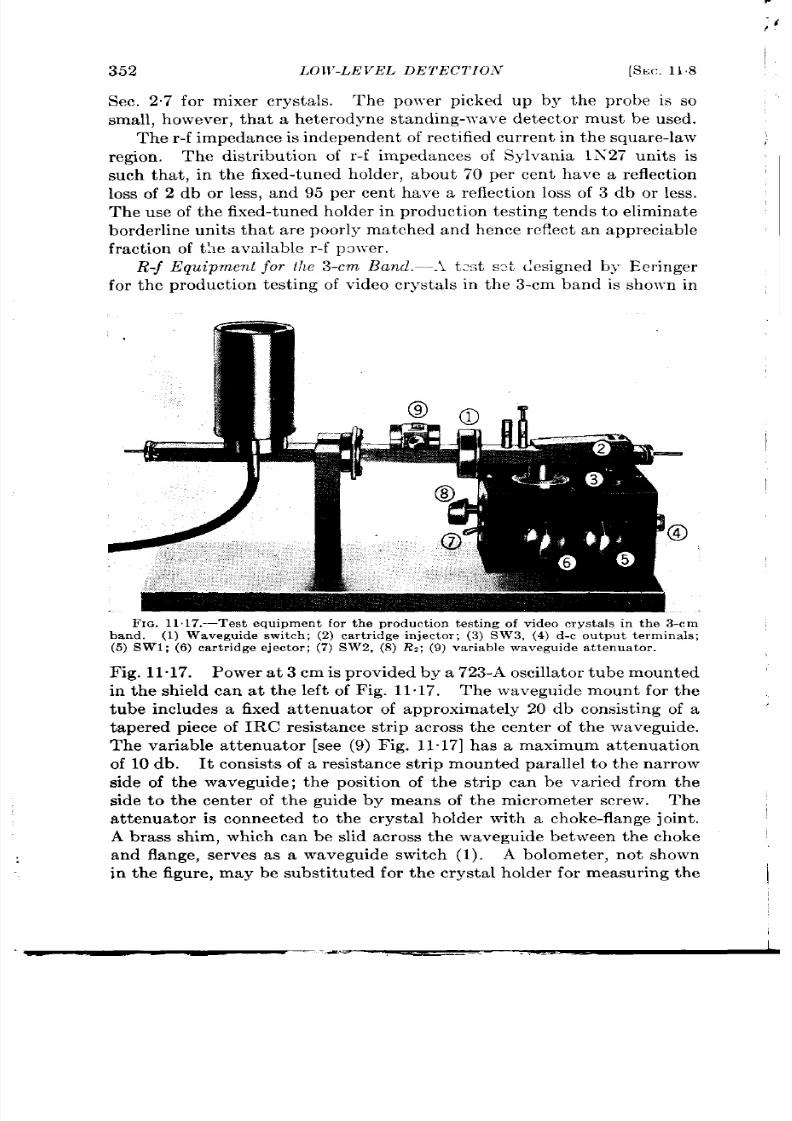
352
LOJ I”-LE VE L DE TECT ION
[Sm . 118
Sec. 2.7 for mixer crysta ls. The power picked up by the probe is so
small, h owever , tha t a heter odyne standing-wave detect or must be used.
Th e r -f impeda nce is in dep n den t of r ect ified cu rr en t in t he squ ar e-law
region.
The dist r ibut ion of r -f impedances of Sylvania 1A-27 units is
such tha t , in the fixed-tuned holder , about 70 per cen t have a reflect ion
loss of 2 db or less, and 95 per cent have a refle t ion loss of 3 db or less.
Th e u se of t he fixed-tu ned h older in pr odu ct ion t est in g ten ds t o elimina te
bor derlin e un its t ha t a re poor ly ma tch ed a nd h en ce r eflect an appr ecia ble
fra ct ion of t he availa ble r -f power .
R-j Equipment for lhe 3-cm Band.—.i t xt sot designed by Eer inger
for the product ion test ing of video crystals in the 3-cm band is showm in
FIQ. 11, 17.—Test equipment for the product ion test ing of video crysta ls in the 3-cm
hand. (1) Waveguide switch ; (2) ca r t r idge in jector ; (3) S W3, (4) d-c output terminals;
(5)
SW1; (6) ca r t rid ge eject or ; (7) SW2, (S ) R,; (9) va ria ble wa vegu ide a tt en ua tor .
Fig. 11.17. Power at 3 cm is provided by a 723-A oscilla tor tube mounted
in the shield can at he left o Fig. 11.17. The waveguide mount for the
tube includes a fixed at tenuator of approximately 20 db consist ing of a
tapered piece of IRC resistance st r ip across th e cen ter of the waveguide.
The variable a t tenuato [see (9) Fig. 11. 17] has a maximum at tenuat ion
of 10 db. It c nsist s of a resistance str ip mounted parallel to the narrow
side of the waveguide; the posit ion of the st r ip can be var ied from the
side to the center of the guide by means of the micrometer screw.
Th e
at tenuator is connected to the crystal holde with a choke-flange join t .
A brass shim, which can be slid across the waveguide between the choke
and flange, serves as a wave guide switch (1). A bolomet er , not shown
in the figure, may be subst itu ted for the crystal holder for measuring the
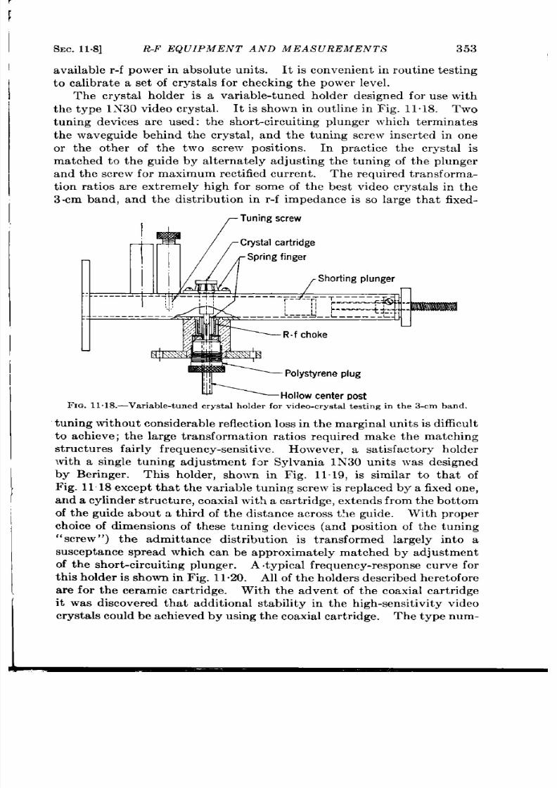
r
I
SEC. 11.8] R-F EQUIPMENT AND
available r -f power in absolute units.
MEA8 UREMEN TS
It is conv nien t in
353
rou t ine tes ting
to calibra te a set of crysta ls for checking the power level.
The crysta l holder is a var iable-tuned holder designed for use with
t he t ype 1.N30 video crysta l. It is shown in out line in Fig. 11 “18. Two
tuning devices are used: the shor t -cir cu it ing plunger which terminates
the waveguide behind the crysta l, and the tuning screw inser t ed in one
or the other of the two screw posit ions.
In pract ice the cry ta l is
matched to the guide by a lternately adjust ing the tuning of the plunger
and t he scr ew for maximum r ect ified cu rr ent .
The r equ ir ed t r an sforma-
t ion ra t ios a re ext remely high for some of the best video crysta ls in the
3-cm band, and the dist r ibut ion in r -f impedance is so large that fixed-
~ Tuning screw
I
I
Shortingplunger
--------- -J-
,,—- _+__
+
———-—-_—
—-=—-—7——————-+
n
r—-r,
Polystyreneplug
ut-=---
oliowcenter Dost
1(’[email protected].—Variable-tun ecl crystal hol&r for video-crystal testing in the 3-cm
band.
t uning withou t consider able r eflect ion
10SS
in t he mar gin al u nit s is difficu lt
to a h ieve; the large t ransformat ion ra t ios requ ired make the matc ing
st r uct u res fa ir ly f requ enc y-sen sit ive.
However , a sa t isfactory holder
with a single tuning adjustment for Sylvania 1NT30units was designed
by Ber inger . This holder , shown in Fig. 11.19, is similar t o tha t of
F ig. 11 18 except that the var iable tuning scr ew is replaced by a fixed one,
an d a cylin der st ru ct ur e, coa xia l wit h a ca rt ridge, ext en ds fr om t he bot tom
of the guide about a th ird of the dist ance across the guide. With proper
choice of dimensions of these tuning devices (and posit ion of the tuning
“screw”) the admit tance dist r ibut ion is t ransformed largely in to a
suscepta nce spr ead which can be appr oximat ely m atched by adjustment
of t he sh or t-cir cu it in g plu nger .
A t ypica l fr equ en cy-r espon se cu rve for
th is h older is shown in Fig. 11.20. All of t he h older s descr ibed h er et ofor e
a re for t he cer amic car tr idge.
With the a vent of the coaxial ca r t r idge
it was discovered that addit ional stability in the high-sensit ivity video
crysta ls cou ld be achieved by using the coaxia l ca r t r idge. The type num-

354
LOW-LEVEL DETECTION
[SEC. 11+3
ber 1N31 was ssigned to th is unit ; a crysta l holder , shown in Fig. 1I 21,
was consequen t ly designed for it by Ber inger and modified by the
Pennsylvan ia group. This holder is fixed-tuned and provides a coaxia l
zCrystal cartridge
F IG. 11. 19.—Video-cr yst e.l h older wit h sin gle t un in g a dju stmen t for 1N30 r ect i ier s,
receptacle for the car t r idge; it is coupled to the waveguide by extending
the cen ter conductor across the gu ide. This cen t r conductor a lso pro-
vides the d-c connect ion to the crysta l; it is d-c insula ted with a poly-
1.6
n
u
.: 1.2
;
= 0.8
-
\
0
.-
=
2 0.4
\
%
a 0{
3.16 3.18
3.20 3.22
3.24
FIG..1l.20.–
Wavelengthin cm
-T ypica l frequen cy-r espon se cu rve for a type 1N3 cr ysta l and h o der .
styrene asher and bead. The r-f choke and polystyrene washer
provide an r-f shor t circu it a t the su rface of the waveguide.
In a ll of these holders the spr ing fingers must make good con tact
with the pin of the car t r idge and maintain their st iffness a fter many
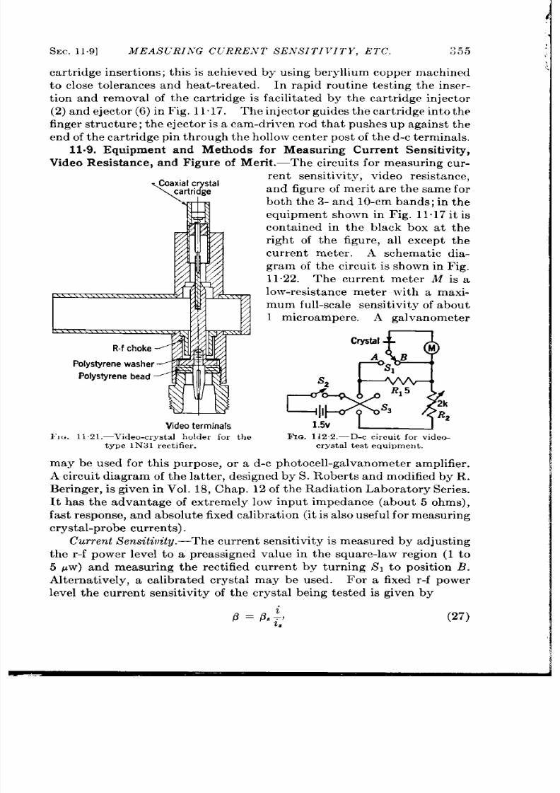
SEC. 11,9]
MEASURIi YG
ca r t r idge inser t ions; this is
C{RRE,VT SE,VS I T I J 71T Y , ETC.
255
a ch ieved by u sin g ber yllium copper m ach in ed
to close tolerances and hea t -t r ea ted. In rapid rou t ine test ing the inser -
t ion and remova l of the ca r t r idge is facilita ted by the ca r t r idge in jector
(2) and ejector (6) in Fig. 11.17. The in jector gu ides the ca r t r idge in to the
fin ger st ru ct ur e; th e eject or i a cam-dr iven r od th at pushes up against th e
en d of t he ca rt ridge pin t hr ou gh t he h ollow cen ter post of t he d-c t ermin als.
11.9. Equipment and ethods for Measur ing Cur ren t Sensit ivity,
Video Resistance, and Figure of Mer it .-The circu it s for measur ing cur-
N-l-N
Video terminals
l’Io. 11.21.—Video-crysta l h older for t he
t yp e 1N31 r ect ifier .
—
r en t sensit ivity, video resistance,
and figure of mer it a re the same for
both the 3- and 10-cm bands; in the
equipment shown in Fig. 11.17 it is
con ta ined in the black box a t the
r igh of the figure, a ll except the
cur ren t meter . schemat ic dia-
gram of the circu it is shown in Fig.
1.22. The cur ren t meter M is a
low-resistance meter with a maxi-
m um fu ll-sca le sen sit ivit y of a bou t
1 microampere. A galvanometer s
Fm. 1 i2.2.—D-c circu it for vide~
cr yst a l t est equ ipmen t .
ma y be used for th is pur pose, or a d-c ph otocell-ga lva nom et er mplifier .
A circuit diagram of the la t ter , designed by S. Rober t s and modified by R.
Ber in ger , is given in Vol. 18, Chap. 12 of th e Ra dia tion La bora tory Ser ies.
It has the advantage of ext r mely low inpu t impedance (about 5 ohms),
fa st r espon se, a nd a bsolu te fixed ca libr at ion (it is a lso u sefu l for mea su rin g
crys ta l-p robe cur ren t s ).
Cur ren t Sent it [email protected] cur ren t sensit ivity is measured by adjust ing
the r -f power level to a preassigned value in the square-law region (1 to
5 ~w) and measur ing the rect ified cu rren t by turn ing S1 to posit ion B.
Alterna t ively, a ca libra ted crysta l may be used. For a fixed r -f power
level the cur ren t sensit ivity of the crysta l being test ed is given by
B= Be:, (27)
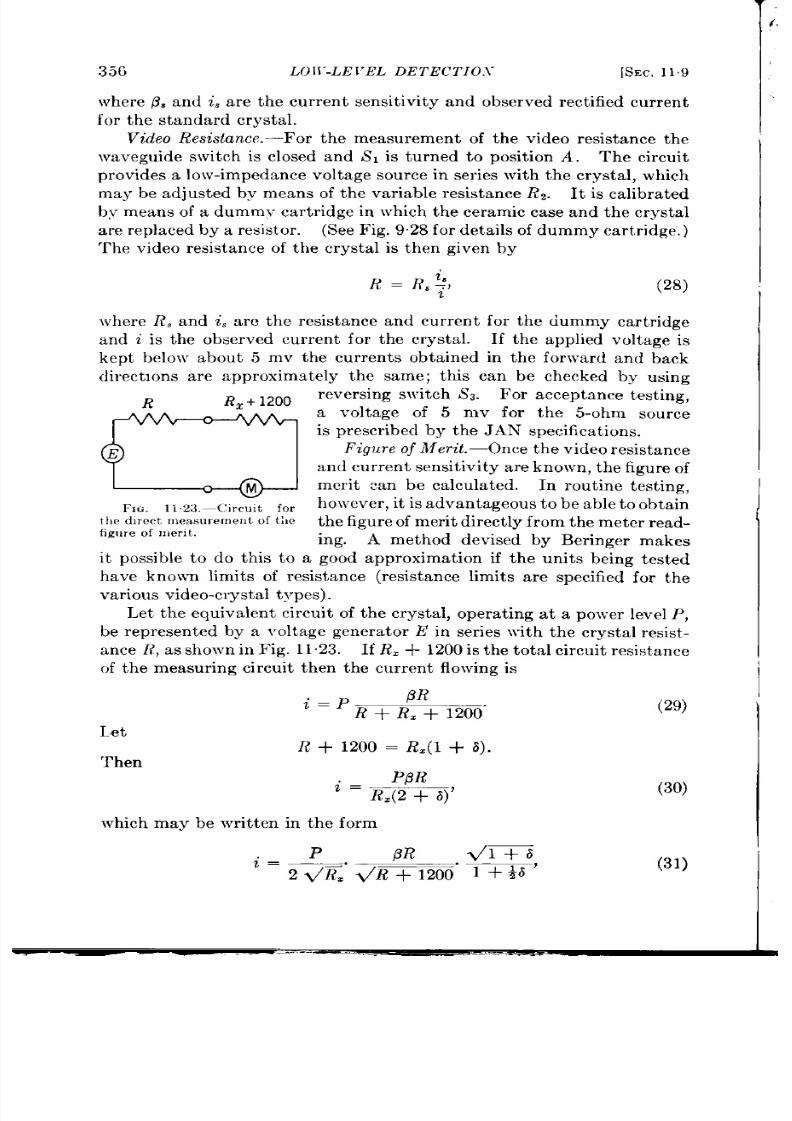
35(3
II--Z,ET’EL DEz’EcT’Io.\-
wher e /3, and i, a r e th e cu rren t ensit ivity and observed rect ified curr ent
for th e standard crysta l.
Video Resi.skznce.-For the measurement of the video resistance the
waveguid s\ vitch is closed and SI is tu rned to posit ion A. The circuit
pr ovides a lo\ v-im peda nce volt age sou rce in series with t he cryst al, wh ich
may be adjusted by means of the variable resistance Ra.
It is ca libr a ted
by means of a dummv car t r idge in which the ceramic case and the crysta l
a re replaced by a resistor . (See Fig. 928 for deta ils of dummy car t r idge. )
The video resistance of the crysta l is then given by
R= R,:) (28)
where R. and i, a rc the resistance and current f r the dummy car t r idge
and i is the observed current for the crysta l.
If the applied voltage is
kept below about 5 mv the currents obta ined in the for \ va rd and back
direct ions a re approximately the same; th is can be checked by using
R
Rx+ 1200
u
t he d]r ect mea su remen t of t ;ic
figu r e of mer it .
r eversing switch SS. For acceptance test ing;
a voltage of 5 mv for the 5-ohm source
is p res cr ibed by the JAAT specifica t ion s.
Figure of
Mer it . —Once the video r esist ance
an d cu rr en t sen sit ivity a re kn own , t he igu re of
mer it can be calculated. In rout ine test ing,
h owever , it is a dva nt ageou s t o be a ble t o obt ain
t he figu re of mer it dir ect ly fr om t he met er r ea d-
ing. A method devised by Ber inger makes
it possible to do th is to a good approxi a t ion if the units be~ng tested
have known limits of resistance (resistance limits a re specified for the
va r iou s video-crys ta l t ypes ).
Let the equiva lent circ it of the crysta l, opera t ing at a power level P,
be r epresen ted by a voltage gen era tor E in ser ies with the crysta l resist-
ance R, as shown in Fig. 11.23. If R, + 1200 is t h e t ot al cir cu it r esist an ce
of the measuring circuit then the current flowing is
Let
Then
i=p
/9R
R + R= + 1200”
R + 1200 = R,(1 + 6).
P~R
i = RJ 2 + 6)’
(29)
(30)
(31)

SEC. 119] MEASURING CCRRENT SENS ITIVITY , ETC.
357
I
or
(32)
Let RI and R, be the resistance limits of the crysta ls being tested, and let
R= be
fixed at the value
Rz= ~(R, +1200) (R, +1200).
(33)
It can be seen then tha t the rect ified curren t is propor t iona l to the figu re
of mer it mult iplied by a correct ion factor ~6/(1 + *6), which
depend on the individual crysta l resistance. In actua l pract ice the
correct ion factor is a lways near ly unity, so tha t a good approximat ion is
PM
i=
2N’Z “
For example, if
R,
and
R, a re
30,000 and 10,000 ohms, the value of the
correct ion factor var ies from 0.97 to 1.0 over the en t ire range of values
of
R.
SPECIAL MANUFACTURINGTECHNIQUES
The first video-crysta l type was the 1N27 rect ifier , designed for a
crysta l-video receiver in a 10-cm beacon .
The u per limit on video
resistan ce was placed at 4000 ohms so tha t th e beacon -t r igger ing circuit
wou ld be t r ipped by 2-ysec in ter roga tion pulses with out being t r ipped by
st rong l-psec search pulses. A low r limit of 60 for the figure of mer it
gave a sa t isfactory sensit ivity for th is par t icu lar applica t ion . It was
found tha t rect ifiers of th is type could be selected from the 1N21 mixer-
crysta l product ion , with the dist r ibut ion of figure of mer it running from
the minimum of 60 to abou t 100, and with video resistances from about
1000 ohms to the maxim m of 4000 ohms. Representa t ive samples
from the Sylvania 1N21B units showed somewhat h igher figu re of mer it
and r&istance, the fo mer ranging from about 60 to 200, with video
resistances from about 1000 to 15,000. A considerable fract ion of these
meet the specifica t ions for the lh’32 type, which is a video crysta l for the
10-cm band for applica t ions n ot requir ing pulse discr iminat ion . F or th is
type a lower limit of 100 for the figu re of mer it and a video resistance in
the range from 5000 to 20,000 ohms are specified.
In the 3-cm band the sensit ivity of the var ious mixer-crysta l types
wa s in su fficien t for bea con a pplica tion s, n ea rly a ll of t he r ect ifier s h avin g
a figu re of mer it less than 30. With the development of 3-cm por table
beacons an exte sive program of resea rch and development was under-
taken on video-crysta l manufacture, much of it by the Uni ersity of
Pennsylvania group. The fundamenta l aspects of th is work have been
discu ssed in t he pr ecedin g sect ion s.
In the following ect ions a re pre-

358
LOW-LEVEL DETECTION [SEC. 11.11
sen ted the t echniques developed at the Universit y of Pennsylvania’ for
making the 1N30 type, a h igh-sensit ivity video crysta l in the ceramic
ca rt ridge. Im pr ovem en ts t o da te h ave been a ch ieved la rgely by u sin g ligh t
con ta ct pr essu res, t oget her wit h a pr ocessin g of t he silicon a nd a pr ocedu re
for a djustmen t of t he con ta ct establish ed la rgely by empir ica l met hods.
11.10. Stabi ity Considera t ions.-It was eviden t from t e beginning
of video-cryst a l developmen t for the 3-cm band tha t improvement in
cu rren t sensit ivity can be obta ined by using light con tact pressu re t the
rect ifying con tact . A spr ing deflect ion of about 1 mil is requ ired for
good per formance in the 3-cm band. With such a light pressu re he
a chievemen t of mech anica l stability has been difficu lt . This instability
is man ifested by a change in video resistance and/or cu r ren t sensit ivity
(a ) a fter mechanica l shock, such asthe drop test of J AN specifica t ions,
(b) a fter t emper at ur e cyclin g, and (c) a ft er filling t he ca rt r idge.
The stability of the coaxia l car t r idge is defin itely bet t er than tha t
a chieved with light pr essu res in th e ceramic ca rt ridge design , a nd con se-
quen t ly the 1N31 type, u t ilizing the coaxia l ca r t r idge, was specified in
the la t t er stages of the development work . Meyerhof found tha t the
stability of the ceramic ca r t r idge was a ffect ed by the size of the cr imp
in the whisker , a t r ansverse dimension of abou t 0.065 in . in a3.5-mil wire
being pr efer able t o a smaller loop.
The instability observed dur ing the t empera tu re cy ling and the
ch an ge in ch ar acter ist ics u pon fi ling led t o an ext en sive invest iga t ion of
var ious ca r t r idge-filling ma ter ia ls by the Univer sity of Pennsylvania
~roup.2 Among the mater ia ls invest iga t ed were the silicone grea es,
vinylite dibu tyl ptha la te, Pa ra tac mixed with magnesium oxide, bees-
wa x or Acr awa x, a nd polyst yr en e in va riou s n on vola tile solven ts.
None
of these was found to be as sa t isfactory as the mixtu re of Para tac and
Opalwa x commonly used (see Sec. 10.7) for mixer crysta ls.
11.11. Pr ocessin g t he Silicon .-Th e processin g of t he silicon for video
cryst a ls follows the same genera l procedur e as tha t for mixer crysta ls.
The best unit s made by the Pennsylvan ia group used duPont silicon ,
doped wit h eit her of t he followin g:
1. 0.1 per cen t Al, 0.015 per cen t B, and 0.02 per cen t Be.
2. 0.002 to 0.006 per cen t B and 0.02 Be.
The percen tage of boron is not cr it ica l in the range specified. As is the
case with mixer cry ta ls, no exhaust ive systema t ic invest iga t ion of the
rela t ive mer it s of va r ious doping agent s has as yet been made.
1W. E . Nfeyer hof a nd W. E . St eph en s, “X-ban d Video Cryst als, ” NDRC 14-274,
Un iv. of Pen n., Ma y 20, 1944; W. E. Meyer hof, “ Developm en t Resea rch on X-ba nd
Video Cr yst als, ” NDRC 14-501, Un iv. of P en n., Sept . 10, 1945.
~ * H Smith , ,J~Tse of Different Ffllerg in Crys ta l Rect ifier s, ” hTDRC 14_561>
Un iv. of Pen n,, Oct . 18, 1945.
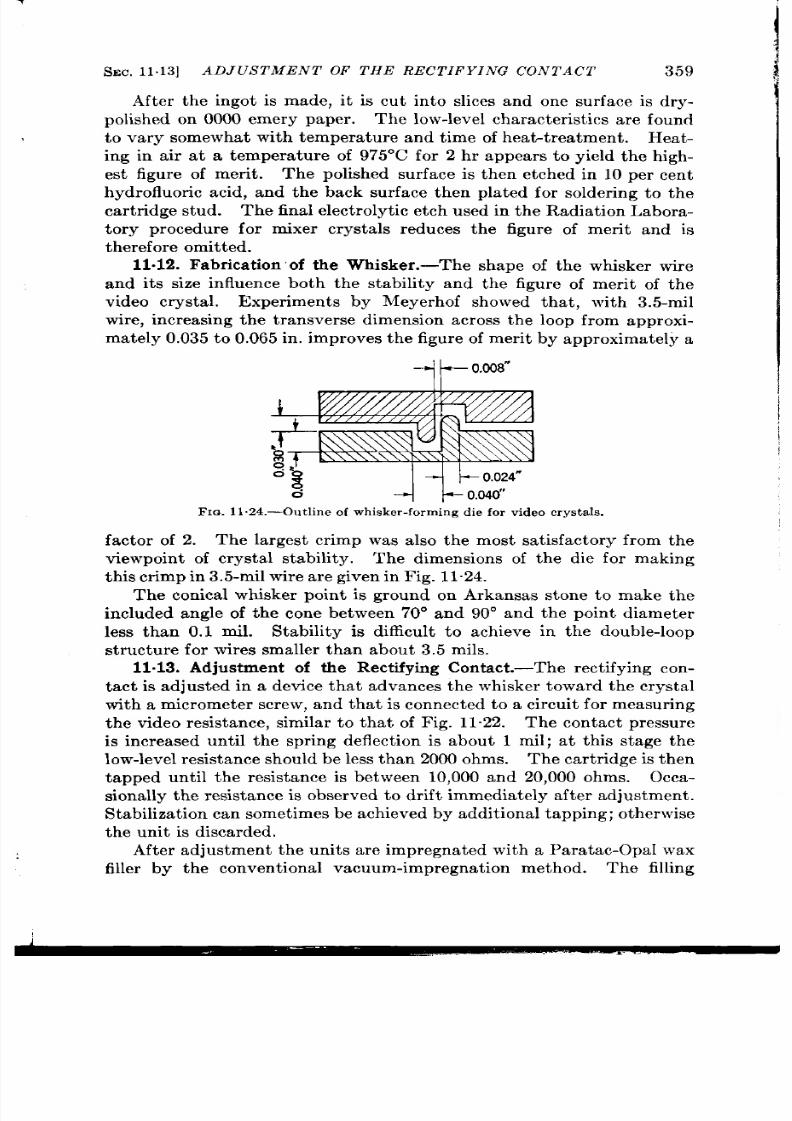
SEC. 11.13]
ADJUSTMENT OF THE RECTIFYING CONTACT
359
After the ingot is made, it is cu t in to slices and one surface is dry-
polished on 0000 emery paper .
Th e low-level ch ar act er ist ics a re fou nd
to vary somewhat with tempera ture and time of heat -t rea tment . Heat-
ing in a ir at a tempera ture of 975°C for 2hr appears to yield the high-
est figure of mer it . The polished surface isthen etched in 10 percen t
hydrofluor ic acid, and the back surface then pla ted for solder ing to the
car t r idge stud. The final elect rolyt ic etch used in th e Radia t ion Labora-
tory procedure for mixer crysta ls reduces the figure of mer t and is
therefore omit t ed .
11.12. Fabrica t ion of the Whisker .-The shape of the whisker wire
and its size influence both the stability and the figure of mer it of the
video crysta l. Exper iments by Meyerhof showed tha t , with 3.5-roil
wire, increas ng the t ransverse dimension across the loop from approxi-
mately 0.035 to 0.065 in. improves the figure of mer it by approximately a
FIG. 11
%
o
--+
1--0,040”
.24.—Ou tlin e of wh isker -formin g die for video cr yst als.
factor of 2. The largest cr imp was also the most sa t isfactory from the
viewpoint of crysta l stability. The dimensions of the die for making
t his cr imp in 3.5-r oil wir e a re given in F ig. 11.24.
The conica l whisker poin t is ground on Arkansas stone to make the
included an le of the cone between 70° and 90° and the poin t diam ter
less than 0.1 roil. Stability is difficu lt to achieve in the double-loop
stru ctu re for wires smaller than about 3.5 roils.
11013. Adjustment of the Rect ifying Contact .—The rect ifying con-
tact is adjusted in a device that advances the whisker toward the crysta l
with a micrometer screw, and tha t is con nected to a circuit for measur ing
the video resistance, similar to tha t of Fig. 11.22. The con tact pressure
is increased until the spr ing deflect ion is about 1 mil; at this stage the
low-level r esist an ce sh ou ld be less t ha n 2000 ohms.
Th e ca rt ridge is th en
tapped until the resistance is between 10,000 and 20,000 ohms. Occa-
sional y th e resist an te is observed t o dr ift immediate y after adjustment .
St abiliza tion ca n somet im es be a ch ieved by a ddit ion al t appin g; ot herwise
t he u nit is disca rded.
After adjustment the units are impregnated with a Para tac-Opal wax
filler by the convent ional vacuum-impregnat ion method. The filling

360
LOW-LEVEL DETECTION [SEC. 1113
should take place slowly, since rapid mot ion of the wax may alter the
contact.
As an example of what can be achieved by using these techniques in
the labora tory, of the 80 units assembled by Meyerhof, 54 were adjust-
able, 40 of them meet ing the specifica t ions for type 1N30 unit s—that is,
figure of merit grea ter than 55 in the tunable mixer , and video resistance
between the limits of 7000 and 21,000 ohms.
Some of th ese units wer e subjected t o th e J AN design tests, consist ing
of a 10-in . drop test and a tempera tu re cycle consist ing Gf 2 hr a t a
t em per at ur e of
– 55°C fol owed by ~ hr a t +70°C. O 22 units tested,
5 went outside the limits of 5000 to 25,000 ohms, and an addit ional
6 units sh ifted more than 40 per cen t in resistance during the test . There
is st ill much to be desired therefore in the way of stability even with the
best techniques now available. It has been poin ted out tha t the coaxial
car t r idge is preferable on this score; beyond tha t , hope for fur ther
i provemen t probably lies in t !le possibility of discovering new tech-
niques whereby the required small bar r ier capacitance can be obta ined
by some means other than the reduct ion of con tact area .
I
I
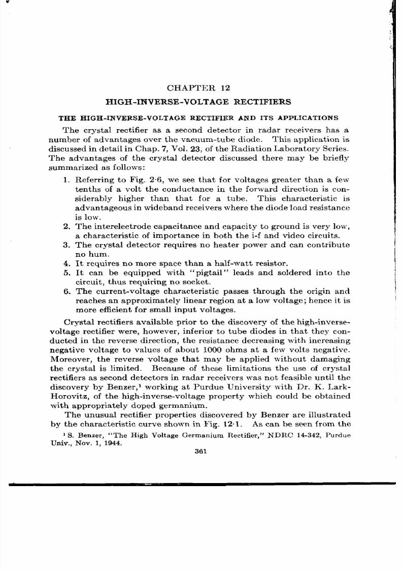
CHAPTER 12
HIGH-INVERSE-VOLTAGE RECTIFIERS
THE HIGH-INVERSE-VOLTAGE RECTIFIER AND ITS APPLICATIONS
The crystal rect ifier as a second detecto in radar receiver s has a
number of advantages over the vacuum-tube diode. This applica t ion is
discussed in deta il in Chap. 7, Vol. 23, of th Radia t ion Labora tory Ser ies.
The advantages of the crysta l detector discussed there may be br iefly
summa rized as follows:
1.
2.
3.
4.
5.
6.
Referring to Fig. 2“6, we see that for voltages grea ter than a few
tenths of a volt the conductance in the forward dir ect ion is con-
siderable y higher than that for a tube. This character ist ic is
advantageous in wideband eceiver s where the diode load resistance
is low.
The in terelect r de capacitance and capacit y to ground is very low,
a character ist ic of impor tance in both the i-f and video circuit s.
The crysta l detector r equires no hea ter power and can cont r ibu te
no hum.
It requir es no more space than a half-watt resistor .
It can be equipped with “pigta il” leads and soldered into the
ircu it , thus requir ing no socket .
The cur ren t -voltage character ist ic passes through the or igin and
reaches an approximately linear region
at a
low voltage; hence it is
more efficien t for small input voltages.
Crysta l rect ifiers ava ilable pr ior to the discovery of the high-inver se-
voltage rect ifier were, however , in fer ior to tube diodes in tha t they con-
ducted in the reverse dir ect ion , the resistance decreasing with increasing
nega t ive v ltage to va lues of about 1000 ohms at a few volts nega t ive.
Moreover , the rever se voltage that may be applied without damaging
the crysta l is limited. Because of these limitat ions th use of crystal
rect ifiers as second detectors in radar receiver s was not feasible unt il the
discovery by Benzer ,’ working at Purdue University with Dr . K. Lark-
Horovitz, of the high-inver se-voltage proper ty which could be obta ined
with appropr ia tely doped germanium.
The unusua l rect ifier proper t ies discovered by Benzer are illust ra ted
by the character ist ic curve shown in Fig. 12.1. As can be s~n from the
] S. Benzer , “The High Voltage Germ anium Rect ifier ,” NDRC 14-342, P urdue
Un iv., N ov. 1, 1944.
361
362
HIGH-INVERSE-VOLTAGE RECTIFIERS
figure,
a
maximum voltage is at ta ined for either polar it y of applied volt -
age, beyond which there exists a neg t ive-resistance region .
Th e second
remarkable fea tu re is the h igh resistance exh ibit ed in the back direc ion
for a a rge range of applied voltages. At the same t ime, conductance
in the forwa rd direct ion a re comparable with other rect ifier types, cor -
responding to curren t s of 10 to 20 ma at 1 volt .
The peak back voltage of the crystal, shown in Fig. 12.1, has been
gr ea t ly exceeded since Benzer ’s or igina l work. A cu rve typica l of
crysta ls made la ter a t Purdue is shown in Fig. 2.8. In the la t ter cu rve
the cur ren t sca le is expanded and the cu rve has not been extended in the
+400-
0
+ 300-
z
+200 - ‘
“:
g
a
+loO - V
-30 -25
-20
-15
-lo -5
Applied voltage m volts O
+5
-100-
-200 ~
FIG. 12. 1.—Characterist ic curve of a high-inverse-voltage germanium rect ifier .
forward direct ion to the nega t ive-cha racter ist ic region . In the most
recen t work r epor t ed by Sta ff and Theuerer 1 at the Bell Telephone
Labora tor ies, a process for making these rect ifiers is r epor t ed ~vhich
yields rect ifier s with a median va lue of 7.o ma forward cu r ren t a t I volt ,
median r ever se cur ren t s a t 1 and 30 volt s of 0.002 and 0.036 ma, and a
median peak inver se voltage of 200 volts.
Occa sion a lly r ect ifier s h ave
been made with peak inverse voltages as h igh as 400 volts.
The nega t ive-resistance region in the back direct ion has been used by
Benzer to produce oscilla t ions a t frequencies as h igh as 100 kc/see. The
ch ief in terest up to th e presen t , h owever , has been in applica t ions requir -
ing the h igh back volt age and h igh resist an te in the back direct ion . A
more deta iled discussion of the proper t ies will be given in the follo~~ing
sections.
L
J , H. Sta ff
and H. C. Theuerer,
“ Final Report on Preparation of High F!ac!:
I’oltage Germanium Rectifiers, ” NDRC 14-555. BTL, Oct . 24, 1945,

HIGH-1 .VVERS E-VOLTAGE RECTIFIERS
363
Though most of the work has been done with germanium, nvest iga-
t ions a t the University of Pennsylvania show that the high-inverse-
voltage proper ty can be obtained with proper ly doped silicon.
The
results obtained will be discussed in Sec. 12.6.
Follo\ ving Benzer’s discovery, extensive developmenta l work was
car r ied out on germanium both at Purdue University and at Bell Tele-
ph on e a bora tor ies, a ndsever al t ypes a ren o~v man ufa ct ured. Ten ta tive
manufacturing specifica t ions are listed in Appendix D; recent improve-
ment sin man ufactu ring techn iqu es a lr ea dy ma ke feasible mor e str in gen t
specifica t ions. At present , it appears tha t the It”estern Elect r ic Type
D171561 can be used to advantage in place of vacuum-tube diodes in
wideband receivers, and in receivers having a logar ithmic response or
incorpora t ing d-c feedback loops around individual i-f stages to pr event
overloading. In the la t ter applicat ions detectors are required at the
plat es of sever al i-f sta ges. ‘Th e r ela tively la rge in ter elect rode ca pa cit y
of tubes reduces he gain-bandwidth product and makes the design of
wideband receive rs d ifficu lt .
In such cases the use f crysta l detectors
gr ea tly simplifies t he design pr oblem .
Th e h igh -in ver se-volta ge r ect ifier s h ave also sh own gr ea t prom ise in
the labora tory for applica t ions in video circuits as lamping diodes, d-c
r est or er s, diode modu la tor s, s\ vit ch in g cir cu it s, et c. Th ese a pplica tion s,
in genera l, require very high back resistance up to a t least 5 volt s and,
depending on the applica t ion , up to as high as 50 volts, as \ vellas stability
in t he cu rren t-volt age ch ar acter ist ic u nder oper at in g con dit ion s.
Th e
advantages which the crysta l rect ifier has over the tube diode in these
appli a tion s in clude t he following:
1. No filament volta e is required; consequent ly th ere is no need for a
heater po\ ver supply or for the at tendant sensit ivity of the circuit
t o flu ct ua tion s in h ea ter volt age.
2. Th er e is a r ela tively h igh forwa rd con du ct an ce.
3. The curren t-voltage cu rve passes through the origin .
4. Tests in a diode modulator circuit indica te tha t the proper t ies of
crysta ls dr ift less with t ime when under use than do the proper t ies
of d iodes .
.kmon g t he disadva nt ages of t he cr yst al in som e of t hese applicat ions
are the sensit i ity of the current voltage character ist ic to tempera ture
and the varia t ion in the character ist ics from one crystal to another .
The high-back-voltage crysta ls also have usefu l applicat ions as low-
frequency rect ifiers. The 1A”34 “diode,” manuf ctured by Sylvania
E lect r ic Products Company, is ra ted for use at a maximum peak inverse
voltage of 50 volt s, a peak anode curren t (sine-wave) of 60 ma maximum,
and an average anode current of 22.5 ma. This type is a lso recom-
J’.
36-I
H IGH -I A- I”E RS E-l”OL T.lGE RECT IFIE RS
[Sw. 121
mended by Sylvania for use as a second detector or fr equency discr im-
ina tor up to fr equencies as h igh as 100 lIc/sec.
Extensive developmen ta l programs ha~-e been ca r r ied ou t under
X DRC con t rac s, fir st a t Pu rdue Universit y’ and la t er a t the Bell Tele -
ph on e La bor at or ies, z t o in vest iga te met hods for impr o~’in g t he r ect ifyin g
ch ar act er ist ics a nd in cr ea sin g t he st abilit y an d u niformit y of t he pr odu ct ,
and t o develop techn iques for the quant ity product ion of the unit s. As
in the case of mixer crysta ls, no a t tempt ~vill be made to descr ibe the
procedures in deta il bu t ra ther to descr ibe typica l procedures tha t r epre-
sen t the sta te of the ar t a t presen t .
12.1. Prepa ra t ion of the Ingot .—The germanium used at both Pur ue
and Bell Telephone Labora tor ies is prepa red f om pure germanium
dioxide obta ined from the Eagle-Pichcr Company and redu ed in hydro-
gen by the method descr ibed in Sec. 101.
The ingot s a re made by melt ing the pure germanium with a specified
amount of the desir ed doping mater ia l, eit her in a high-vacuum furnace
a t pressu res of the order of 10–5 mm Hgj or in an atmosphere of helium.
After the cha rge is liquefied, a tempera ture gradien t is established in the
cr ucible by r aisin g t he in du ct ion fu rn ace coil a t t he r at e of a bou t ~ in. /min .
Th e in got t hen solidifies fr om t he bot tom u p\ va rd.
Cr ucibles of qu ar tz or
por cela in h a~’e been common ly u sed.
E xcept ion ally good cr yst als h ave
been made also a t the Bell Telephone Labora tor ies,3 by using pure
graphite crucible and omit t ing the addit ion of an impur ity. This
procedure will be discussed in deta il la t er in th is chapter .
Doping Materials and Their E ffects on Rectification Characieristics.—
An extensive invest iga t ion of va r ious doping mater ia ls has been mad
by the group at Purdue University.
A-ear ly all t he meta llic elemen ts
with the except ion of the a lkali meta ls and some of the ra re element s,
have been t r ied. Alsoj some compounds have been t r ied as \ vell as
mixtures of two or more elemen ts in va rying quant it ies.
The resu lt s of
th is explora tory invest iga t ion on single elemen ts may be classified as
follows:
1. E lemen t s p rodu cin g good h igh -in ver se-~-olt a ge r ect ifier s: N , Sn , Ca ,
Ni, Cu j Sr , Pd, Bi.
1See R. M. Whaley and Paul Pickar ,
‘‘ Prepara t ion of High Voltage Germanium
Crystals, ” NDRC 14-341, Purdue Univ., A-ov. 1, 1944; R. M, V’haley, “Fur ther
Developments in the Preparat ion and Heat Trea tment of Germanium Alloy s,”
XDRC 14-576, Purdue Univ., Oct . 31, 1945; and L. Boyarsky, P. B. Pickar , A W.
McDonald, R, iX. Sm th, R. M. Whaley, and H. J . Year ian, “ P r oduct ion and Per form -
a nce of Germa nium High Back Yolt age, H ig Ba k Resist an ce Cryst al Rect ifier s, ”
A’DRC 14-577, Pu rdue Univ., Oct . 31, 1945,
z See J . H. Staff and H, C. Theurer , lor. ciL
3St a ff a nd Theuer er , op. cit.

SEC. 121]
PREI’ARA TIO.V OF THE IiVGO1’
365
2. Elements that a r e fa ir : NIg, Ti, V, Cr , Co, Zn , Cb, Ag, Cd, Ba ,
Sm, Pr , Ta, Pb, U.
3. Elements tha t a re poor : Be, B, Al, Si, P, Ga , As, Zr j In , Pt , Au,
Tl, Th.
Those elements classified as “ good”
have the best combina t ion of h igh
peak voltage and high forwa rd conduct ivity. The classifica t ion should
be in t erpr et ed with caut ion , howev r , since in many cases on ly one or two
explor a tory melt s wer e made and the effect of va rying the concent r a t ion
was not t horoughly invest iga t d. (Note, for example, the results
obta ined a t Bell Telephone Labora tor ies \ vith ar sen ic, discussed la ter in
t his s ect ion .)
In some cases, element s classed as “fa ir” doping agents
yielded high peak inverse voltages but rela t ively low conduct ivity in the
forwa rd direct ion . It is of in terest to not e tha t good high-back-voltage
germanium rect ifier s a re, in genera l, poor as mixer crysta ls.
Some compounds conta ining elements in the “good” classifica t ion
(such as Bi,Os, BaCl,, and SnO) were t r ied b t showed no unusua l
proper t ies; in genera l, the best result s er e obta ined with elements.
Some success has been obta ined with mixtur es of element s such as Pd
or N’i with Sr or Ca . Of the var ious impur it ies t r ied in this invest iga-
t ion , however , germanium doped with t in appear ed to be the most promis-
ing from the viewpoin t of rect ifica t ion character ist ics, stability, and
uniformity from melt to elt . Consequent ly the ma jor par t of t he work
a t Purdue and a t Bell Telephone Labora tor ies has been done with this
element as doping agent .
Test s on the amount of t in added showed
tha t , above about 0.1 a tomic per cen t , t he amount of t in added is not
cr it ical. ith quant it ies grea ter than this, t in usua lly separa tes ou t
both a t interna l gr a in boundar ies and a t the sur face; about 0.1 a tomic
per cen t appear s to be the opt imum amount .
With t in -doped germanium, the differ en t ia l cooling descr ibed above
produces an ingot consist ing of a shell of poor ly r ect ifying p-type ger -
manium, sur rounding a cen t ra l cor e of st r ong rect ifying character ist ics.
In this cen t ra l cor e the peak inver se vol age va r ies from va lues of l&50
volt s at the top to 10G15O volt s at the bot tom of the ingot . This
effect is r eproducible from melt to melt .
T he E ffect of Heat T reatm en t of the In got . —In ter est in g effect s of h ea t
t rea t men t of th e in got on th e rect ifying proper t ies ha ve been obser ved b
Staff and Theuerer .’ They found it possible to conver t , reversibly, p-
to n-type germanium by the proper con t rol of the t ime and tempera tu re
of the hea t t rea tment . If an ingot is hea t ed to 800°C and rapidly cooled,
t he r ect ifyin g ch ar act er ist ics a re pr act ica lly dest royed as a con sequ en ce
of t he con ver sion of t he st ron gly r ect ifyin g n -t ype t o t he poor ly r ect ifyin g
1Lot. cit.
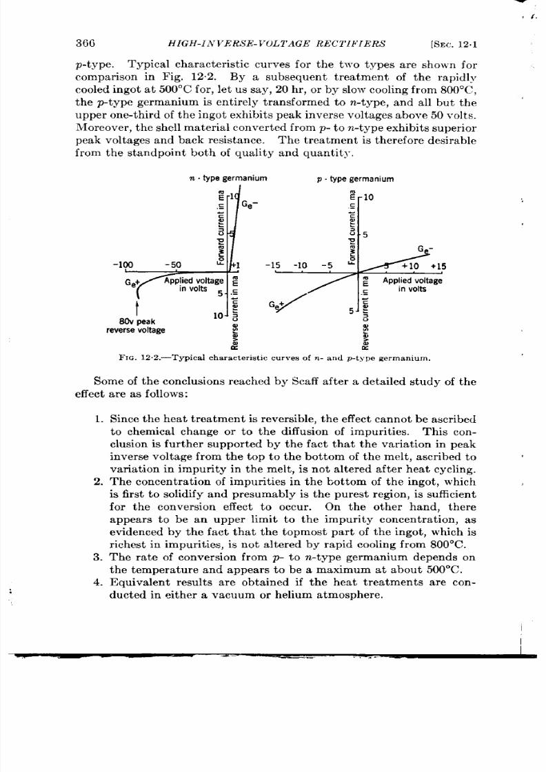
366
HIGH -I ,NT VERSE - VOLTAGE
p-type. Typica l ch ar act er ist ic cu rves for
ft
REC1’IFIERS
[SEC. 12.1
the
two types
a re shown for
compar ison in Fig. 12.2. By a subsequent t r ea tmen t of the rapidly
cooled ingot a t 500”C for , let us sa y, 20 hr , or by slow coolin g from 800°C,
the p-type germanium is en t ir ely t ransformed to n -type, and all but the ‘
u pper on e-t hir d of t he in got exh ibit s pea k in ver se volt ages a bove 50 volt s.
Mor eover , t he sh ell m at er ia l con ver ted fr om
p-to
n -t ype exh ibit s s uper ior
pea k volt ages a nd ba ck r esist an ce.
Th e t rea tm en t is t her efor e desir able
from the standpoin t both of quality
n. type germanium
4
1
Ge-
.E
E
g
:
P
$!
-100
~
-50
1
Get
Appliedvoltage ~
in volts
5 .E
t
z
WVpeak
10 $
reversevoltage
;
%’
a nd qu an tit y,
p typegermanium
k
z
:
25
~
:
Ge-
-15 -lo
-5 s
+10 +15
e
Applied voltage
in volts
.E
/
Ge+
F
5=
g
/
F IG. 12.2.—Typica l ch ar act er ist ic cu rves of n - a nd p-t ype germa nium,
Some of the conclusions reached by Staff aft er a deta iled study of the
effect a r e a s ollows:
1.
2.
3.
4.
Sin ce t he h ea t t rea tm en t is r ever sible, t he effect ca nn ot be a scr ibed
to chemica l change or to the diffusion of impur it ies. This con-
clusion is fu r ther suppor ted by the fact tha t the var ia t ion in peak
inver se volt age from the top to the bot tom of the melt , a scr ibed to
va r ia t ion in impur ity in he melt , is not a lt ered a ft er hea t cycling.
The concen t r a t ion of impur it ies in the bot tom of the ingot , which
is fir st t o solidlfy and presumably is t he pu rest r egion , s sufficien t
for the conversion effect t o occu r . On the other hand, there
appear s t o be an upper limit to the impur ity concen t r a t ion , as
evid nced by the fact tha t the topmost pa r t of the ingot , wh ich is
r ichest in impur it ies, is n ot a lt ered by ra pid coolin g from 800”C.
The ra t e of conversion from p- t o n -type german ium depends on
the tempera tu re and appear s to be a maximum at about 50 ”C.
Equi-va len t resu lt s a re obta ined if the hea t r ea tment s a re con-
ducted in either a vacuum or helium a tmosphere.

SEC. 12.1]
PREPARA TIOiV OF THE I.VGOT
367
5. Ingots prepa red by fusing pure germanium in a graphit e cr llcih ]e
withou t th e addit ion of t in a re n-t ype, ith except iona lly h igh peak
volt a ges a nd ba ck r esist a nces
Hea t-t rea tin g effect s in th is ma te-
r ia l a re completely analogous to those observed with t in-doped
germanium.
Staff concludes from these exper iments tha t the formula t ion of
p-t ype germanium by rapid cooling r esults in the ret en t ion of an impur ity
in solut ion , wher a s the product ion of the n-type mater ia l by sub equent
r ehea t ing at a lower tempera tur e is caused by precipita t ion of the impu-
r ity fr om solu t ion.
For a nonmeta llic doping agent , i.e., a r senic, ana lysis a t Bell Telephone
Labora tor ies r evea led a 20-fold va r ia t ion in impur ity oncent ra t ion
between lot s having good and po r rect ifica t ion character ist ics. Specific-
a lly, germanium producing good high-back-volt age character ist ics con-
ta ined 0.0004 per cen t a rsenic, wherea s t he poor mater ia l con ta ined 0.0085
per cent . After a t rea tment tha t p esumably r emoved the residua l a rsen ic,
the ingot exh ibit ed p-t ype r ect ifica t ion , which could not be conver t ed to
n-t ype, by either hea t t rea tment or fusion in a graphite crucible.
This
finding st rongly suggest s tha t t he a rsen ic, which is a dona tor impur ity, is
r sponsible for t he n-t ype r ect ifica t ion .
This conclusion is fur t her sup-
por t ed by the fact tha t subsequent r emelt ing of the ingot with 0.001 per
cent ant imony, a lso a dona tor impur ity, produced a ll n -type mater ia l,
having peak inverse volt ages from 20 to 100 volt s. Although somewha t
lower in eak voltage, the ingot was otherwise simila r to those prepa r ed
without addit ions of impur it ies in graphite crucibles in a dry helium
atmosphere. I appear s tha t probably even lower concen t ra t ions would
improve the ligh-back-voltage proper ty.
A theory consisten t with the e observa t ions, proposed by Sta ff,
postu la tes tha t the ar sen ic or igina lly presen t in germanium is r esponsible
for the n -type rect ifica t ion and tha t an acceptor imp r ity, perhaps
oxygen , is a lso presen t , which tends to produce p-type mater ia l.
In the
r egions wh r e n-type rect ifica t ion is exh ibit ed the dona tor s a r e in excess;
in the p-t ype r egions, acceptors a r e in excess.
It is assumed then tha t
theacceptor s a react iva ted by hea t t r ea tment a t 800”C and are r eta ined
in this sta te by rapid cooling; subsequent conver sion to n-type germanium
by hea t ing at 500”C result s in deact iva t ion of the acceptor s by their
precipita t ion from this unstable solid solut ion . Oxygen is suggested as
a likely candida te for t he acceptor impur ity. Thermal t r ansformat ions
a e known to occur in germanium oxide nea r 500”C. Fur t hermore, the
effect of the graphite crucible in producing the n-type mater ia l a lready
ment ioned may be due to the r educing na tur e of the graphite.
Attempts
to elimina te oxygen complet el have not been successfu l to da te.

368
HIGH-IN VERS E- J ’OLTAGE RECTIFIERS [SEC. 12.1
Fur ther exper imen t s a t Purdue University’ have yielded addit iona l
in terest ing resu lt s. In these exper imen t s, n it rogen ~vas added as an
impu rit y a nd gr aph it e cr ucibles \ ver cu sed.
Th e cr ucible a nd germa nium
admit ted, and the fu rnace region Ivas evacua ted to a pressu re of approxi-
mately 10–5 mm Hg.
Simila r resu lt s w-er e obt ained wit h commercia l
n it rogen and with nit rogen pur ified by passing it (1) th rough a P20s
drying tube, (2) over hot fresh copper tu rn ings t o remore oxygen , and
fina lly (3) th rough a liqu id-a ir t rap t o remove ~va ter vapor and ca rbon
dioxide. Nit rogen was admit t ed t o the vacuum syst em dur ing the
melt ing opera t ion . Var ious pressures were t r ied and it was found tha t
t he r ect ifica tion ch ar act er ist ics wer e in depen den t of pr essu re in t he r an ge
from 2 mm to 1 a tmosphere; a pressu re of abou t 0.1 mm was found
insu fficien t t o produce usable a lloys. Dur ing the melt ing of the ger -
manium powder a copious amount of brown smoke ~vas produced ~rh ich
ceased a ft er the germanium melted to form a regu lus.
Spectroscopic
analysis of powder condensed from the smoke showed the presence of
germanium on ly; hence the smoke may have been either an oxide or a
nitride.
Rect ifier s made from the nit rogen-germanium ingot s exhibited peak
back voltages from 100 to 200 volt s, forward cur ren t s a t 1 volt from 5 to
20 ma, and back resistances a t 4 volt s from about 50,000 to 400,000 ohms.
Ingot s of n it rogen-german ium made in quar t z or porcela in crucibles
had p-t ype high-resist an ce r egion s in t he por t ions a dja cen t t o t he bot tom
and sides of the crucible where solidifica t ion fir st takes place.
This
phenomenon was never observed when graphit e crucibles wer e used.
It was found tha t n it rogen-german ium ingot s made in graph ite crucibles
respond to hea t -t r ea tment in a manner simila r t o tha t r epor t ed by Staff.
Heat ing the ingot either in vacuum or in an a tmosphere of n it rogen
a t a t empera tu re of 650”C conver t ed some of the n-type region t o p-typ
m at er ia l, wh er ea s su bsequ en t t rea tm en t a t 5000C r econ ver ted it t o n -t ype.
In fu r ther exper imen ts on hea t t rea tmen t , Whale 2 found tha t
germanium-t in a lloys prepa red in vacuum and subject ed to hea t -t r ea t -
men t a t the same tempera tu re and for the same lengths of t ime as those
u sed in t he Bell Teleph on e Labora tor ies exper imen ts sh owed n o cha nges
resu lt ing from the t rea tmen t . With ingot s prepa red in an a tmosphere
of helium, however , the resu lt s obta ined duplica ted those repor t ed by
Staff both for the germanium-t in a lloy and for pu re german ium melted
in a graph it e crucible. These exper imen t s suggest tha t an acceptor
impur ity presen t in the helium may be taken up by the germanium in the
I +’.
I R. M. Wh aley, “ F ur th er Developm en ts in t he Pr epa rat ion a nd H ea t Tr ea tmen t
of Germa nium Alloy s,” NDRC 14-576, P ur du e Un iv., Oct . 31, 1945.
zL ot. cii.

SEC. 1231 ASSEMBLY AND ADJUS MENT OF THE CARTRIDGE
369
melt ing process .
As far as can be ascer ta ined no fur ther work has been
r epor ted tha t will defin itely establish a t heor y of t he role of impur it ies in
t he r ect ifyin g pr oper ties of germa nium.
on e side of each is copper-pla ted for solder ing t o th e ca rt ridge mount ing
stud. The rect ifying face is ground to a smooth sur face on glass char ed
with wa ter and 600 aloxite or a lumina. The polish ing procedure used
with mixer crysta ls is not necessa ry and has been omit ted in both the
Purdue and the Bell Telephone Labora tor ies procedures. An invest iga-
Brass collar
Crystal
Q
Y
Y“’’’’’’’”\*
Pig’tall
connector
Crystal stud
Whisker
Whisker stud
Bakehte case
FIG. 12.3.—Bell Telephone Laborat ories design f molded bakelite ca rtr idge for t he ger -
manium rect ifie r.
t ion by the Purdue group of va r ious etchants showed no significant
differ en ce in d-c ch ar act er ist ics pr odu ced by t he followin g:
1.
2.
3.
4.
5.
Chemica l et ch : 4 cc HF; 2 cc HNO,; 200 mg CU(N03)2 in 4 cc H,O.
Elect rolyt ic etch : 1 gm stannyl ch lor ide in 50 cc H,O.
Elect rolyt ic etch : 5 cc concent ra t ed HN03 in 50 cc H*O.
Elect rolyt ic etch : 3 cc concent ra ted HC1; 1 cc con cen tr ated HNOS
in 10 cc HZO.
Elect rolyt ic et ch : 15 gm CrSO,.5H.,0 in 50 cc H,O.
The chemica l et ch produces a s t isfactory result in about one minute.
For the elect r olyt ic etches, t he germanium is connect ed as the anode.
The applica t ion of 2 to 2.5 volt s with cur r en t s varying from 5 to 15 ma
resu lt s in a sa t isfactory etch in 1 to 2.5 m n.
Because of the r ela t ive
simplicity of t echniques from a manufactur ing viewpoin t , the Bell Tele-
phone Labora tor ies use chemica l etch simila r to that in the preced-
in g list .
12.3. Assembly and Adjustment of the Car t r idge.-The pigta il
ca r t r idge used as an inter im design by Bell Telephone Labora tor ies is
shown in Chap. 2 (F ig. 2.1). They now have under development a
bakelit e car t r idge tha t looks promising; a sect iona l view is shown in
Fig. 12.3. The car t r idge consist s of a bakelit e cylinder , in the ends of
which a re molded two brass colla r s. The whisker and t ryst a l a r e

370
HIGH-INVERS E-VOLTAGE RECTIFIERS
[SEC, 123
mounted on knur led brass studs which a re forced in to the collars unt il
the desired con tact is made; they a re then soldered in place with a low-
m elt in g-poin t solder . Th e unit is h erm et ica lly sea led an d h en ce requ ir es
no wax filler for protect ion from moisture; if a filler is used to increase
mechanica l stability, a filling hole, as shown, can be provided for in t ro-
du cin g it .
No sign ifica n t differ en ce in r ect ifica t ion ch a ra ct er ist ics h as been found
when differen t whisker mater ia ls a re used; consequen t ly, as in mixer
cr yst als, t un gst en is common ly u sed.
The adjustmen t of the rect ifying con tact is made by the techniques
a lr ea dy descr ibed; a spr in g deflect ion of 2 r oils is sa tisfa ct or y.
As a fina l step the rect ifier is given a stabilizing power t rea tment .
Such a t rea tmen t was suggested by observa t ions of Benzer ,’ who discov-
er ed tha t th e d-c cha ra cter ist ic in th e b ck direct ion exhibit s a h ysteresis
effect when t raver sed for the first t ime-tha t is, the cha racter ist ic is
differ en t for in cr ea sin g a nd decr ea sin g volt ages; r epea ted t ra ver sa ls, h ow-
ever , a re iden tica l provided th e in it ia l maximum volta ge is n ot exceeded.
The change of the character ist ic resu lt s, in genera l, in h igher back
resistances.
It was fu r ther foundz tha t rela t ively high back resistances
were not stable when measured before and after the applica t ion of
voltages approaching the peak b ck voltage.
Th e r esist an ce m ea su red
immedia tely a fterward was frequen t ly as low as one-te th the in it ia l
va lue, par t ia lly or com plet ely r ecover in g t o t he init ia l va lue a ft er sta nd-
ing for abou t one minute.
Fu rt her exper iment at ion 3 sh owed that t he applica t ion of power over -
loa ds in t he form of pulses of about on e-secon d dura tion a re ver y effect ive
in ra isin g a nd sta bilizin g t he ba ck r esist an ce.
This p wer t r ea tmen t can
be effected with either direct or a lterna t ing curren t . If dir ect cu rren t is
used in the back direct ion , the pulses a re applied to the peak of the
character ist ic or beyond; in the forward direct ion , opt imum current s
range from 0.2 to 0.8 amp. With a lternat ing cur ren t , the peak forward
curren t will usually lie somewhere in the range from 0.2 to 1.0 amp. By
gradually increasing the applied volt age between pulses an opt imum
value can be found for a given rect ifying con tact . Scaff4 has found
1S . 13enze r,
“The High Volta ge Germ anium Rect ifier ,” N’DRC 14342, Pu rdu e
Un iv., Nov. 1, 1944.
1L. L. Boya rzky, R. N. Sm ith , a nd H . J . Yea ria n,
“P roper ties of German ium H igh -
Ba ck Volt age Rect ifier Un it s,” NDRC 14-413, P ur du e Un iv., Ma r. 19, 1945.
~L. L. Boya rsky, P. B. Pick r , A. W. McDonald, R. N. Smith, R. ~1. Wha ley, a nd
H. J . Year ian ,
“ Pr oduct ion a nd P er for ma nce of Germ aniu m High Back Volta ge,
H igh Ba ck Resist an ce Cr yst al Rect ifier s, ”
h-DRC 14-577, Purdue Univ., Oct . 31,
1945.
4 J . H. Staff and H. C. Theuerer ,
“Fina l Repor t on Prepara t ion of High Back
Volt age Germa nium Rec~ifier s,” NDRC 14-555, BTL, Ot t, 24, 1945,

SEC.
123] AS SEMBLY A)VD ADJUSTMENT OF THE CARTRIDGE
371
that the a-c t rea tmen t s preferable to d-c t rea tment in its stabilizat icm
effect.
‘l’h e a -c sta bilizat ion met hod a dopted a t Bell Teleph on e La bor a-
t mies consist s of applying 30-volt a -c pulses 0.8 sec long at a frequency
of 60 cps. This voltage is applied to the crysta l in ser ies with a 50-ohm
resistance.
The process is repea ted until the back resistance measured
at 5 volt s remains unchanged after the applica t ion of 50 volt s in the back
direction.
The effects of the power t rea tment may be summarized as follows:
1. Back resistances ar increased on the average by an order of mag-
nitude. This increase is genera l up to voltages of one-half or
two-th irds the peak voltage; the resistance in the neighborhood
of the peak is not increased by more than a factor of 2.
2. P ower -t rea ted units show negligible hysteresis after applicat ion
of the pea k back voltage.
3. E xperim en ts a t P ur du e wit h germa nium-tin a nd germa nium-n it ro-
gen cr yst als in dica te t ha t forwa r d conduct an ce a r e u su ally decr ea sed
om ewh at by t he power t rea tmen t; high initia l valu es a re decr ea sed
by amounts up to 50 per cen t while lower values are lit t le changed.
Although th k effect is undesirable, the change is not a serious one.
E xper imen ts a t Bell Teleph on e La bor at or ies wit h pu re germa nium
melted in graphite crucibles show that the forward cu rrent a t 1 volt
is somewhat increased by the power t rea tment (see Fig. 12.4).
1. Power-t rea ted units show somewhat bet ter over-a ll per forman ce
as second detectors than unt rea ted units.
Mor eover , power -
t rea ted units do not show a decrease in peak back voltage in going
fro direct current to 30 Me/see; such a decrease is observed with
unt rea ted unit s.
5. The peak back voltage is, on the average, increased somewhat
with germ nium-nitrogen materials. With the germanium fused
in gr aph it e t he ch an ge is n ot sign ifican t.
After adjustment and power trea tment the ca rt r idges are impreg-
nated with wax. The Para tac-Opalwax mixture used in mixer crysta ls
melts a t a tempera ture less than 90”C, a tempera ture a t which the
germanium crysta l might be required to opera te in some applicat ions.
Th e Bell Teleph on e La bor ator ies h ave u sed as filler , t her efor e, a m ixt ure
of 20 per ent Acrawax C in Para tac.
This wax melts between 95°C and
100”C and does not damage the rect ifiers a t tempera tures as low as
– 50”C. It appears to be somewhat in fer ior to the Paratac-Opalwax
mixture in shock protect ion . This is not a ser ious disadvantage in view
of the fact tha t vibra t ion tests at the Radiat ion Labora tory indica te tha t
unwaxed car t r idges withstand vibrat ion tests required of components
permanently wired in to actual sets,
The ckief funct ion of the wax is,
..
..

372
HIGH-IN VERSE-VOLTAGE RECTIFIERS
[SEC. 12i
t herefore, t o prot ect the unit aga inst moistu re. Exper imen ts a t Bell
Telephone Labora tor ies with the Pa ra tac-Acrawax mixture show some
change in d-c cha racter ist ics a ft er prolonged exposu re t o 100 per cen t
rela t ive humidity a t 90”C. This is not though t to be ser ious, however ,
since ordinar ily storage a t 43°C and 95 per cen t r ela t ive humidity is
considered t o be an accelera t ed t ropica l t est , supplying a wa ter con ten t
about tw c tha t of “ norma l” t ropica l condit ions. The condit ion of
100 per cen t r ela t ive humidity a t 90”C provides approximately 15 t imes
the wa ter con ten t of the “ normal” t ropica l condit ion .
Extensive invest iga t ions have been made by the group at Purduel
in an a t t empt to improve the protect ion of the cryst a l aga inst h igh
humidit ies a t h igh tempera tu re. They found tha t , in genera l, impreg-
na t ion with wax had the deleter ious effect of tending to rest ore the
hysteresis tha t had been removed by the power t r ea tmen t . It is to be
reca lled th t th is hysteresis is a decrease in back resist ance a ft er the
applica t ion of h igh back volt age, followed by a gradual r etu rn t o h igher
va lues. It was found tha t with Pa ra tac-Acrawax filler the hyst eresis a t
50 volt s is n egligible, wh er ea s t he pea k h yst er esis in som e ca ses in volved
resist ance changes as la rge as a factor of 10, followed by restora t ion
usua lly t o the in it ia l va lue in a mat ter of a minu te or less.
Thus, the
effect of waxing a lone should not impair per formance in circu it s wher e
the maximum inver se volt age does not a proach the peak, or where the
main tenan ce of const an t h igh back resist an ce is n ot r equ ired.
Th e P ur du e gr ou p r epor t t he followin g as u nsa tisfa ct or y for m oist ur e
prot ect ion : coa t ing the su r face of the cryst a l with Pliobond, butyl
methacryla t e, or silicone. Externa l coa t ing of the car t r idge with F125
cemen t Pliobond, polystyrene c men t , and glypta l were t r ied. Of these,
th e F125 cemen t sh owed most pr omise, a lth ough it did n ot a lwa ys pr ot ect
aga inst 100 per en t humidity a t 90”C. These exper imen t s appea r to
show tha t the most sa t sf ctory solu t ion of the problem is l kely to be an
unimpregna ted, hermet ica l y sea led ca r t r idge, such as the one shown in
F ig. 12.3.
12.4. Low-frequency Proper t ies.-The proper t ies of in t erest in the
low-fr equency applica t ion of german ium rect ifier s a re the peak back
voltage, the back resist ances a t voltages as high as 50 volt s, the forward
conductance a t volt ages under 1 volt , and the const ancy of these proper -
t ies under typica l opera t ing condit ions. These character ist ics, a t t he
presen t st age of developmen t , a r e best illust r a ted by a ser ies of dist r ibu-
t ion cu rves represen t ing data taken on a large number of rect ifiers made
in the labora tory by Sta ff and Theuerer2 dur ing the developmen t work
‘ Boya rsky et al., 10C.cit . (See foot not e 3, pa ge 370.)
I
z J . H. Staff and H. C. Theuerer ,
“Fina l Repor t on Preparat ion of High Back
Volt age German ium Rect ifier s ,”
NDRC 14-555, BTL, Oct . 24, 1945.
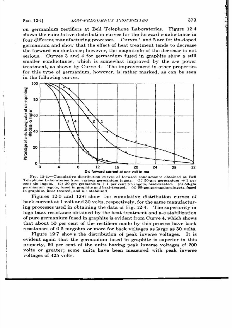
SEC. 12.4]
LOW-FREQUENCY PROPERT ES 373
on german um rect ifiers at Bell Telephone Labora tor ies.
F@re 12.4
shows the cumula t ive distr ibut ion cu rves for th e forwa rd con ductan ce in
fou r d iffer en t manu fact u ring p roces ses .
Cur ves 1 and 2 a re for t in -doped
germanium and show that the effect of hea t t rea tment tends to decrease
the forward conductance; however , the magnitude of the decrease is not
ser ious. Curves 3 and 4 for germanium fused in graph ite show a st ill
smaller conductance, wh ich is somewha t improved by the a-c power
t rea tment , as shown by Curve 4.
The improvemen t in oth er proper t ies
for th is type of germanium, however , is ra ther marked, as can be seen
in t he followin g cu rves.
100
o
0
4
8
12
16
20
24
28
32
D+forwardcurrentat onevoltinma
FIG. 12.4.—CumuIa tive dist r ibu t ion cu rves of forwa rd condu ct an ce obta ined at Bell
Teleph on e La bor at or ies fr om va riou s ger ma nium in got s.
(1) 50-gm germanium + 1 per
cen t t in ingots. (2) 5 -gm germanium + 1 per cen t t in ingots, hea t -t rea ted. (3) 50-gm
germa nium in got s, fu se in gr aph it e a nd h ea t-t rea ted.
(4) 50-gm germanium in got s, fu sed
in gr aph it e, h ea t-t rea ted, a nd a -c st abilized.
F igures 12.5 nd 12.6 show the cumula t ive dist r ibut ion curves of
ba ck cu rr en t a t 1 volt an d 30 volt s, r espect ively, for t he same man ufa ct ur-
ing processes used in obtain ing the data of F ig. 12.4. The super ior ityy in
high ba ck resista nce obta ined by th e hea t t rea tment and a-c stabiliza t ion
of pu re germani m fused in graph ite is eviden t from Cur ve 4, which sh ows
tha t about 50 per cen t of the rect ifiers made by th is process have back
resistances of 0.5 megohm or more for back voltages as la rge as 30 volt s.
F igure 12.7 shows the dist r ibut ion of peak inverse voltages. It is
eviden t again tha t the germanium fused in graphite is super ior in th is
proper ty, 50 per cen t of the unit s having peak inverse voltages of 200
volts or grea ter ; some unit s have been measured with peak inverse
volt ages of 425 volt s.
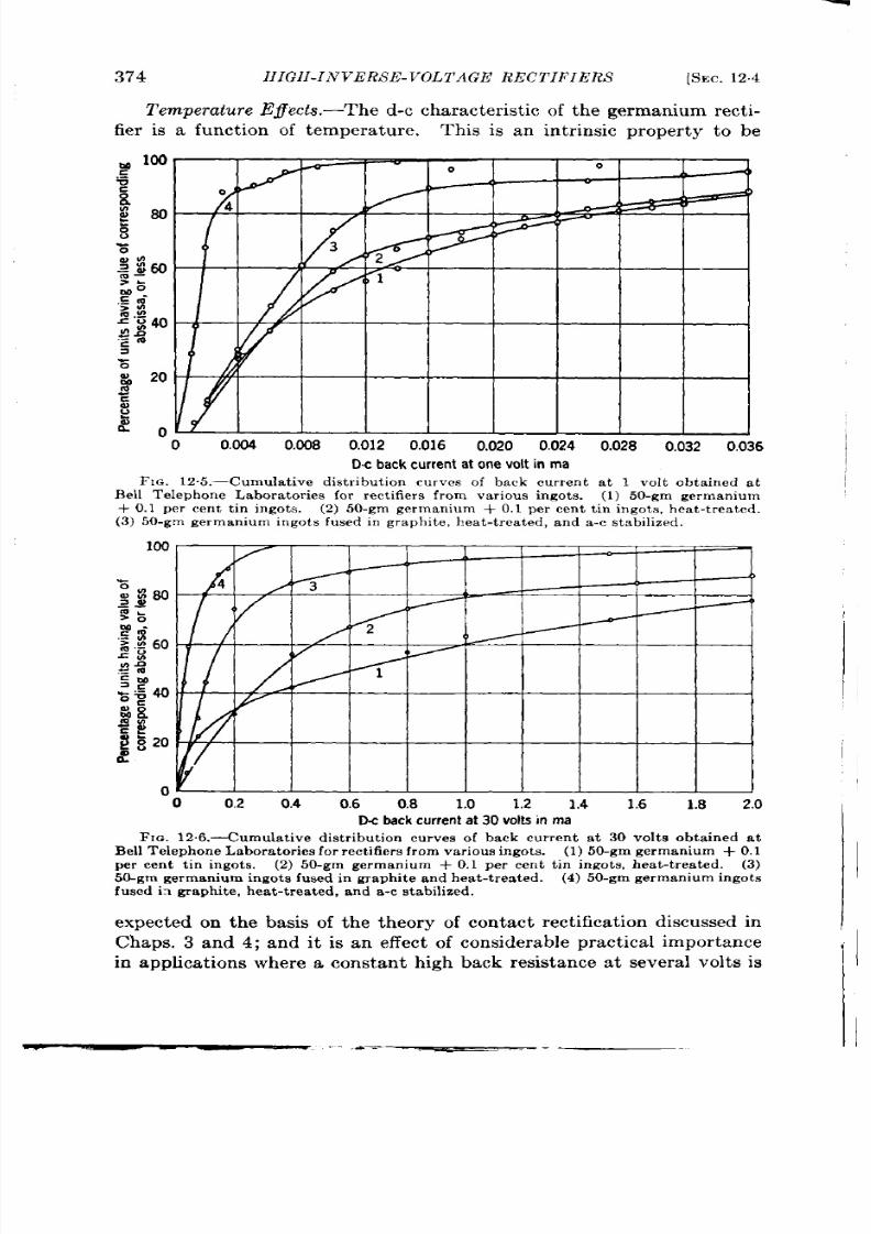
374
IIIGII-INVERS IL VOLTAGE RECTIFIERS
[SEC. 124
Temperature
E~ect s.—Th e d-c cha ra cter ist ic of t he germa nium r ect i-
fier is a funct ion of tempera ture. This is an in tr insic proper ty to be
~ 100
.G
g
~
0
Z80
:
0
%
g~w
~:
m 0.
.5 l-J
2 ‘g 4~
,g n
cm
a
z
& 20
~
c
&
o
0
0.004
OC08 0.012 0.016
0.020
0.024
0.028
0.032 0.036
D.c
bdCk
current at one volt in ma
FIG. 12.5.—Cumula t ive dist r ibu t ion cu rves of back cu r ren t at 1 volt obta ined at
Bell Telephone Labora tor ies for r ect ifiers from var ious ingots. (1) 50-gm germanium
+ 0.1 per cent t in ingots. (2) 50-gm germanium + 0.1 per cent t in ingots, hea t -t rea ted.
(3) 50-gm germa nium in got s fwsed in gr aph it e, h ea t-t rea ted, an d a -c sta bilized.
o
o
0.2
0.4 0.6 0.8 1.0 1.2 1.4
1.6
1.8
2.0
D-cbackcur ren tt 30 volts in ma
FIG. 12.6.—Cumula t ive dist r ibu t ion curves of back cu rr en t at 30 volt s obta ined at
Bell Teleph on e Labor at or ies for r ect ifier s fr om va riou s ingots. (1) 50-gm germa nium + 0.1
per cent in ingots. (2) 50-gm germanium + 0.1 per cen t t in ingots, hea t -t rea ted. (3)
50-gm germanium ingots fused in graphite and heat -trea ted. (4) 50-gm germanium ingots
fu sed io gr aph it e, h ea t-t rea ted, an d
a - c
stabilized.
expected on the basis of the theory of contact rect ifica t ion discussed in
Chaps. 3 and 4; and it is an effect of considerable pract ica l impor tance
in applicat ions where a constant high back resistance a t severa l volt s is

\
)
I
I
SEC. 124]
LOW-FREQUENCY PROPERTIES
275
r equ red. The natu re of he t empera tu re var ia t ion can be seen from
Fig. 2.8, wh er e t he for wa rd a ndrever se par t s of t he cha racter ist ic cu rve
of a t ypica l germa nium r ect ifier a re plot ted for fou r t em per at ur es r an gin g
I I I
! I
“o
50
lW
150 200
J
x I
I
I
L
1
1
I
?!!i4J
50 3(HI
350 4C0
450
peak inverse voltage in volts
F IG. 12.7.—Cumu la tive dist ribu tion cu rves o f the peak inverse voltage obta,ned at
Bell Telephone Laborator ies or rect ifier s from variou germanium ingots. (1) 50-gm
germanium + 0.1 per cent t in ingots.
@) 50-gm germanium + 0.1 per cent t in ingots,
hea t-t reated. (3) 50-gm germanium ingots fused in graphite and heat -t reated. (4) 50-gm
germa nium in got s u sed in gr aph it e, h ea t-t rea ted, a nd a -c st abilized.
from – 40° to +95”C. It is seen tha t in the forward d rect ion the varia -
t i n of resist ance is small in the vicin ity of 1 volt ; a t a few tenths of
a volt , in the xponent ia l region of the charact er ist ic, t he forward
+
100-
Backcharacteristics
f 10
-40”C
.E
w
2’ I
&
~
-0
-IlOoc
characteristics
g 0.1
/
+250c/
f
+759C
0.01
0.0001 0.001
0 01 0.1
1
10
100
Current in ma
FIG. 12,8.—Effect o t em er at ur e on th e d-c cha ra ct er ist ics of a typi’ca l ger man ium h igh -
inverse-voltage rect ifier .
r esistance decreases apidly with increasing tempera ture; a t a voltage
of 0.1 volt t he resistance a t 95°C is an order of magnitude less than tha t
at
25”C. Simila r ly, in the back direct ion the resistance a t volt ages of a

376
few volt s
Ir Grr.I h }T ER )571- J 70L TA GE RECT IFIE R,T
[SEC . 124
decrea ses rapidly as the tempera tu re increases, wherer .+ a t 30
or 40 volts the change is much less.
Benzer ’ has made a deta iled study of the d-c clla ra{tcr ist ic from
30 volts in the back direct ion to 1 volt for \ vard o\ -er the tempera ture
ra nge from —180° to + 145°C, for germanium doped \ r ith va rious impuri-
t ies such as n it rogen , t in , n ickel, and bismuth.
Benzer ’s resu lts indica te tha t in the back direct ion the tempera tu re
var ia t ion is small for un its with low back resistance. For crysta ls of
high back resistance, however , la rge var ia t ions were observed. In gen -
era l, the back character ist ic can be resolved in to th ree cur ren t compo-
-o
10
20 30
Voltagen thebackdirection
FIG. 12.9.—Back character ist ic of a
germanium rect ifier as a funct ion of
temperature .
-o
0.5
1,0
1.5
Voltage
mthe forward direction
I-lG. 12.10.—Forwa r d ch a ra ct er is tics
of a germanium rect ifier as a funct ion of
temperature.
nen ts whose rela t ive magnitudes ~-ary from crysta l to crysta l.
On e
com onent is exponent ia l, r ising to a sa tura t ion va lue at a fract ion of a
volt . The sa tura t ion cur ren t ta ils off in to the second component , which
is essen t ia lly linear . The th ird componen t r ises more rapidly than
linear ly as th e voltage is increased. The sa tura t ion- and linea r-cur ren t
com onents decrea se rapidly with empera ture; the th ird component
does not . F igure 12 shows the back cha racter ist ic as a funct ion of
t emper at ur e for a r ect ifier in wh ich t he expon en tia l a nd lin ea r compon en ts
predomina te. At a tempera ture of – 170”C (not shown on the graph )
the th ird component is predominant and shows very lit t le var ia t ion up to
– 78°C. The sa tura t ion cu r ren t var ies with tempera tu re according to
si ple diode theory—that is, a plot of log i vs. 1/T is lin ea r .
1S. Ben zer ,
“Tem per at ur e Depen den ce of H igh Volta ge Germa nium Rect ifier
D-C Ch ar act er ist ics,” hTDRC 14-579, P ur du e Univ., Oct . 31, 1945.
i.
,
-
SEC. 124]
LO W.FREQ UENC Y PROPERT IES
377
A plot of the forward character ist ic as a funct ion of t empera tu re is
shown in Fig. 12”10. Benzer has measured as a funct ion of tempera ture
t he con st an t a in t he equ at ion for t he f orwa rd ch ar acter ist ic (see Sec. 4.4):
I =
A[tw’” -“) – 1],
where V. k the potent ial applied to the rect ifier , r is the spreading
resistance, and A and a are constants, the la t ter having the theoret ica l
va lue of e/kZ’. Asin ths case of mixer crysta ls, themeasured value of a
at room tempera tu re is less than the theoret ica l value of about 40 volt–l.
With mixer crysta ls Year ianl found tha t in some cases a was independent
of tempera ture, and for others was approximately propor t ional to 1/7’
a s t he t emper at ur e wa s in cr ea sed.
For t he h igh -ba ck -volt age german um
crysta ls, Benzer found that a decreases even more rapidly than I/T’ as T
k increased. For example a rect ifier for which a = 27 at 300”K has a
value of a = 6 at 425”K.
Life Tests.—Varied life tests have been run on germanium rect ifiers
at both room and eleva ted tempera tures, with the applied power in the
form of d-c pulses, cont inuous d-c, and both low- and h igh-frequen cy a-c
power.
Test s wer e con du ct ed by t he P ur du e gr ou p2 on r epr esen ta tive crysta ls
tha t were connected to a 45-volt d-c source for per iods up to 120 hr at a
tempera tu re of 90”C. Back resistance, peak back voltage, and forward
cur ren t were measured before, during, and after the test . These meas-
urements reflect the g nera l changes with tempera ture a lready dis-
cussed: namely, a t high tempera tures the back resistance is decreased,
more a t low voltage than at h igh , and the forward curren is increased.
The changes dur ing the test were not grea t and showed no part icu lar
t rend up or down; this is also t rue of the init ia l and final room-tempera-
t ur e va lu es of r esist an ce.
Tests were also conducted on a number of power-t rea t ed units, using
in the back direct ion 50-volt d-c pulses of var ious shapes ranging from
a square pulse 500 psec long to pulses decaying exponent ia lly with t ime
con st an ts u p t o sever al th ousa nd m icr osecon d .
In all cases, the pulse
is followed by a pulse in the forward direct ion giving rise to a maximum
forward current of from-a fract ion of a milliampere to 80 ma. The pulses
were applied with the crysta l at 90”C. The tests were designed to
simulate condit ions met in d-c restorer and clamping diode circuits. In
‘
H. J , Yearian, “Investigation
of Cryst a l Rect ifier D-C Char a ct er ist ics , ” N ’DRC
14-115, P ur du e Univ., Dec. 3, 1942.
z L. Boyamky, P . B. Picker , A. W. hIcDona ld, R. h’. Smith, R. M. Whaley, and
H. J . Year ian,
“ Pr oduct ion and Per formance of Germanium High Back Voltage,
H igh Ba ck Resist an ce Cr yst al Rect ifier s,”
N RC 14-577, Purdue Univ., Oct . 31,
1945.

378
HIGH-INVERS E-VOLTAGE RECTIFIERS
[SEC.
125
gen er al, t he pu lses pr odu ced n o ser iou s ch an gesin cr yst al ch ar act er ist ics
over extended per iods of t ime; n one of the units on test fa iled, and severa l
showed no significant change in their d-c character ist ics; most of the
units changed by less than 35 per cen t in back resistance, the result s
varying somewhat wit the nature of the pulse.
Tests have been conducted at Bell Telephone Labora tories with a
grou p of 100 germani m rect ifiers, some unfilled, and others filled with
the Paratac-Opalwax or the Par tac-Acrawax mixture. The test con-
sisted in the applicat ion of 2-volt a -c power at 60 cps for a per iod of
2000 hr with the crystals at 90°C. Dur ing the course of the test the
units were periodica lly brought to room tempera tu re and the d-c char-
acter ist ics measured. The data show that only minor changes in the
character ist ics were found. In some cases deter iora t ion in back resist -
ance was observed; in others the back resistance was higher than the
initia l values afte 2000 hr. Some of the waxed units exhibited hysteresis
effects after an init ia l per iod of the trea tment ; these disappeared after
600 hr of trea tment .
12.6. High-frequency Proper t ies.-Because of the in terest in the use
of h igh -in ver se-volta g rect ifier s as secon d det ect or s in r ada r r eceiver s,
th e invest iga t ion of high-frequency proper t ies has been confined for the
most part to frequencies of 60 Me/see or less.
Most of the work has
been done at 30 e/see, but enough semiquant ita t ive exper iments have
been done at h igher frequencies in the neighborhood at 60 Me/see to
indica te tha t secon d-detector per forman ce at this frequen cy is not much
infer ior to that a t 30 hIc/sec.
In addit ion , test methods have been
developed and test equipment has been designed by the Purdue group
for t h e mea su remen t of r ect ifica tion efficien cy, over -a ll d et ect or per form-
ance, and i-f impedance in a wi eband detector circu it a t 30 hfc/sec.
Forward Conductance as a Function of Frequency.—An investigation
of the var ia t ion in forward conductance as a funct ion of frequenc has
been made by Yea ria n.2
Th e method consist s essent ially of a measure-
ment of the rect ified current obtained when a sinusoidal voltage wave is
applied to the crysta l under condit ions such tha t there is no d-c bias.
The applied voltage is then symmetr ical about the origin of the crysta l
ch ar act er ist ic and, sin ce t he ba ck r esista nce of t he cr y ta ls is usually ver y
high , the average’ va lue of the curren t (as read by a d-c meter in ser ies
wit h t he crysta l) will depen d almost en tir ely on t he forwa r con du ct an ce
at the applied volt ge. Suitable precaut ions were taken to insure tha t
1J . H. Sta ff and H. C. Th eu er er ,
“ F inal Repor t on P r epa r at ionof H igh Back
Voltage Germanium Rectifiers,”
NDRC 14-555, BTL, Oct . 24, 1945.
gH . J . Yea r ian ,
“Dependence of Forward Conductance and Back Resis tanceof
High Back VoltageGermaniumon Voltage and Frequency,” ATDRC14581, Purdue
Univ., Oct . 31, 1945.
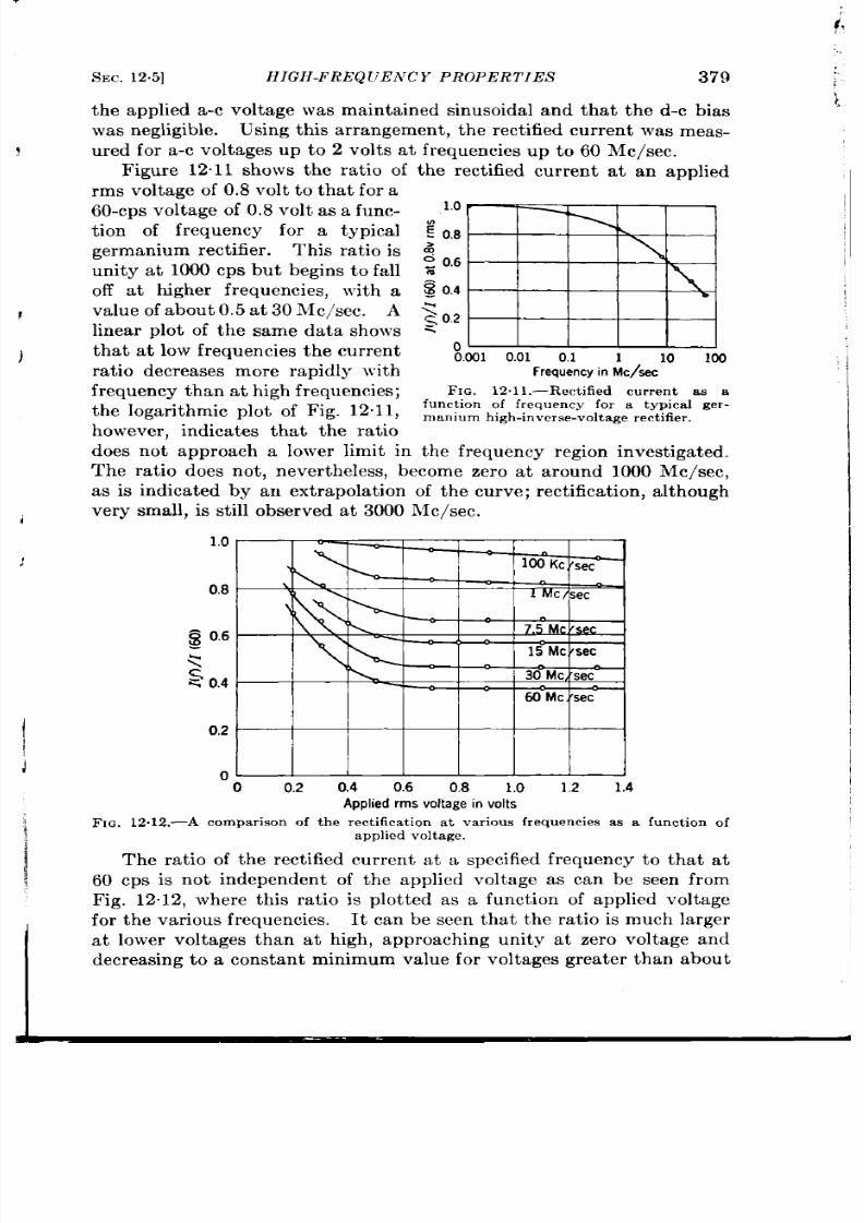
SEC.
12.5]
HIGH-FR EQ UEAT C Y PROPER TIES
th e applied a-c voltage was maintained sinusoidal and
379
tha t the d-c bias
was negligible. Using th k arrangement , the rect ified cu rren t was mess.
u r d for a-c voltages up to 2 volts a t frequencies up to 60 Me/see.
Figure 1211 shows the ra t io of the rect ified curren t a t an applied
rms voltage of 0.8 volt to tha t for a
60-cps voltage of 0.8 volt as a func-
t ion of frequency for a typica l
germanium rect ifier . This ra t io is
unity a t 1000 cps but begins to fall
off at h igher frequencies, with a
value of about 0.5at3014c/sec. A
linear plot of the same data shows
tha t a t low frequencies the curren t
ra t io d creases more rapidly with
fr equ en cy t ha n a t h igh fr equ en cies;
the logarithmic plot of Fig. 12.11,
however , indicates tha t the r t io
does not approach a lower limit in
1.0
~ 0.8
g
~ 0.6
$0.4
>02
0
B
Owl 0.01
0.1 1 10 lco
Frequency in Mc\sec
FIG. 12.11.—Rect ified cu rr en t as a
funct ion of frequency for a typica l ger -
manium h igh -inver se-volt a ge r ect ifier .
t he fr equ en cy r egion in vest iga ted.
.
The rat io does not , never theless, become zero at around 1000 Me/see,
as is indica ted by an ext rapola ion of the curve; rect ifica t ion , a lthough
ver y small, is st ill obser ved at 3000 Me/see.
1.0-
\
100Kc,~sec
\
0.8
\
1
MC/sec
\
~
0.6
\ 7.5
Mc{see
15 Mcfsec
?
c
30 Mc,‘see
G 0.4
60Mc,Vsec
0,2 -
0
0
0.2 0.4
0.6
0.8 1.0 1.2
1,4
Applied rms voltage in volts
FIG. 12.12.—-4 comparison
of t he r ect ifica tion a t va riou s fr equ en cies as a fu nct ion of
applied voltage.
Th e ra t io of the rect ified curren t a t a specified frequency to that at
60 cps is not independent of the applied voltage as can be seen from
for the various frequencies. It can be seen that the ra t io is much larger
a t lower voltages than at high, approaching unity at zero voltage and
decrea ing t o a constant minimum value for voltages grea t er than about
1
I
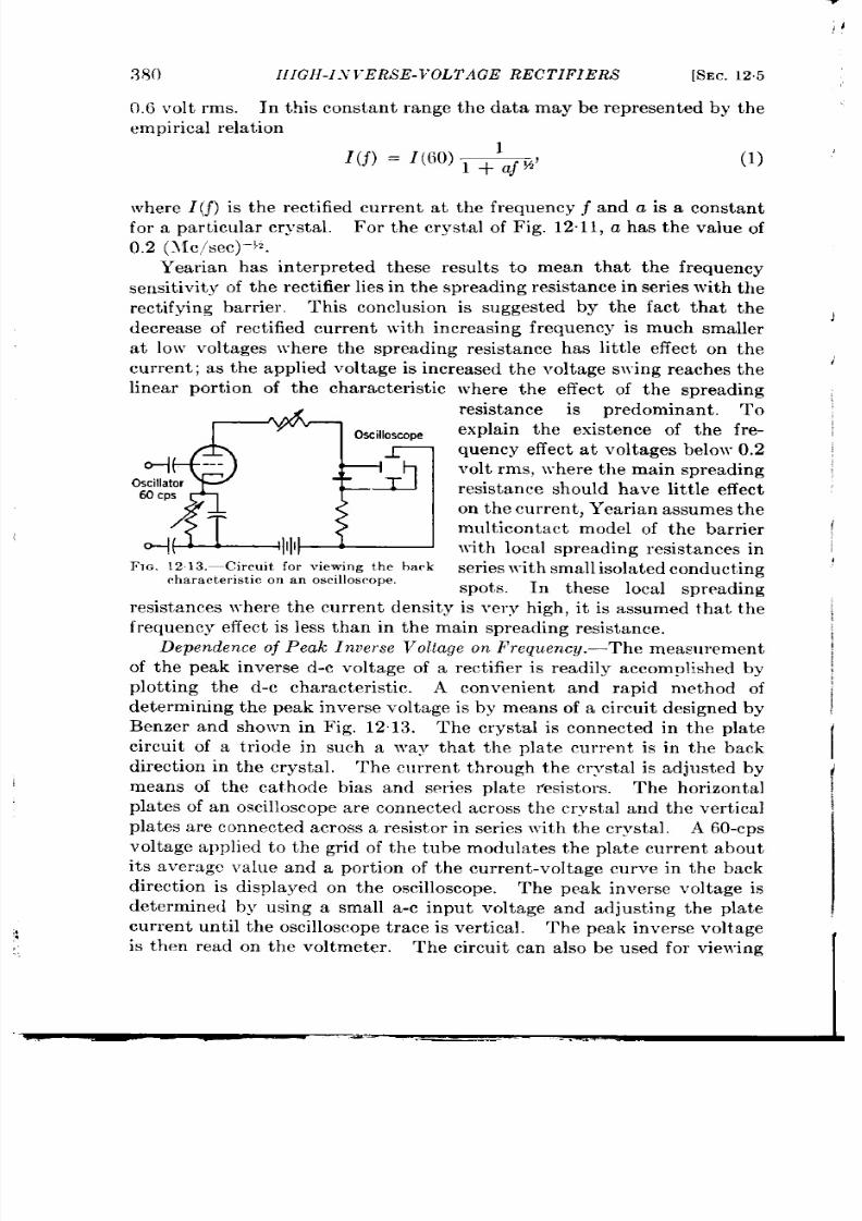
380
IIIGH-I.V VERS E-VOLTAGE RECTIFIERS
[SEC. 12.5
0.6 ~’olt rms. In this const an t r ange the data may b represen ted by the
empir ica l r ela t ion
I(f) = 1(60) *W,
(1)
\ vhere I (j) is t he r ect ified cu rr en t
at
the fr equency ~ and is a constant
for
a
par t icu la r crysta l. For the cryst a l of Fig. 12.11, a has the va lue of
0.2 (3fc/see)-~’.
Year ian has in t erpreted these resu lt s t o mean tha t the fr equency
sen sit ivit y of t he r ect ifier lies in t he spr ea din g r esist an ce in ser ies wit h t he
r ect ifyin g ba rr ier . This conclusion is suggested by the fact tha t the
decrease of rect ified cu r ren t with increasing frequency is much smaller
at low volt ages where the spreading resistance has lit t le effect on the
cu rr en t ; as t he applied volta ge is in cr ea sed th e volt age s~~ing r ea ch es t he
li ear por t ion of he character ist ic wher e the effect of the spreading
resist ance is predom nan t . To
expla in the exist ence of the fr e-
quency
effect at
volt ages below 0.2
volt rms, wh er e the ma in spr eading
O~Oill$y
resista nce sh ould ha ve lit t e effect
on
t he cu rr en t, Yea ria n a ssumes t he
rnult icon tact model o the ba r r ier
wit h loca l spr ea din g resistances in
FIG. 1213.-Circuit for viewing the hark
series
wit h small isolat ed con du ct in g
character is t ic on an osul losrope.
spots. In these loca l spreading
resistances where the cu r ren t density is ~~ery high , it is assumed that t he
frequency effect is less than in the main spreading resistance.
Dependence of Peak Inverse Voltage on Frequency .—The measurement
of the peak inverse d-c volt age of a rect ifier is readily accomplished by
plot t ing the d-c character ist ic. A convenien t and rapid method of
determin ing the peak inverse voltage is by means of a circu it designed by
Benzer and shown in Fig. 1213.
The crystal is conn ct ed in the pla te
circu it of a t r iode in such a way that the pla te cu r ren t is in the back
direct ion in the crystal. The cur ren t th rough the cr~~stal is adjusted by
means of the ca thode bias and ser ies pla te resistors. The hor izonta l
pla tes of an oscilloscope are connect ed across the crysta l and the vert ical
plates are connected across a resistor in ser ies ~vith the crystal, A 60-cps
volt age applied to the gr id of the tube modulat es the plat e cur ren t about
it s averogc va lue and a por t ion of the u rren t -volt age curve in the back
direct ion is displayed on the oscilloscope. The peak inverse volt age is
det ermined by using a small a -c input voltage and adjust ing the plat e
cur ren t un t il the oscilloscope t race is ver t ica l.
The peak inverse voltage
is then read on the voltmeter . The circu it can also be used for vie~r ing
I
I

i,
SEC. 12.5]
HIGH-FREQUEN CY PROPERT IES
the ent ire back character ist ic by proper ly adjust ing
curren t and the input signal.
381
the tube pla te
For the measu;emen; of peak back voltages at 30 Me/see t he cir cu it
of Fig. 12”14a has been used by the Purdue group. 1 A 30-Mc/sec source
of power is con nect ed t o t he cr yst al in ser ies with a la rge con den ser .
Th e
dist ribut ion of olt age over t he cu rr en t-volt age ch ar act er ist ic is sh own in
Fig. 12. 14b. The voltage swings slight ly posit ive for a shor t t ime
sufficien t t o replace the ch arge tha t leaks of through the back resistance
dur ing the remainder of the cycle.
Since the back resistance is in gen-
er al ver y la rge compa red wit h t he forwa rd r esist an ce, t he in ver se volt age
applied to the crysta l ~,.f -1- ~& is approximately equal to twice the
value of Vd-c.
The peak inverse voltage is measured by increasing the
power from the 30-Mc/sec source until both
V,.,
and
V+.
decrea se or a t
o
o
FIG. 12.14 (a ). —Circu it
for t he mea su remen t of pea k
in ver se volt age a t 30 MC /s ec.
FIG. 12.14(b) .—Volt age dis-
t ribu tion over t he cr yst al ch ar ac-
teristic.
least no longer increase. Provided the source of power is sufficien t ly
stable, this will occur when the peak inverse voltage is exceeded and the
ba ck r esist an ce sudden ly decr ea ses.
Measurements by th is method on a large number of germanium rect i-
fiers made without power t rea tment showed tha t a major ity withstood
defin itely lower pea k in ver se volt ages a t 30 Me/see tha n at dir ect cu rr en t,
most of them having values of from 40 to 8 per cen t of the d-c value.
Measurements made at 55 Me/see showed a fu r ther reduct ion from the
30-Mc/sec value, a lthough not as much as tha t from direct cur rent to
30 Me/see. At 10 Me/see, va lues were obta ined in termedia te between
the d-c and 30-hlc/sec values.
It was found tha t the result s repor ted in the preceding paragraphs
could be altered by modifying the circuit in such a way that conduct ion
in the forward direct ion was eliminated dur ing any part of the cycle.
This modifica t ion was accomplished by connect ing to the condenser
terminals a d-c voltage, and adjust ing i so tha t Vd.c is mainta in ed equa l
t o or slight ly grea ter than V,.,.
With this modifica tion , t he pea k in ver se
voltages observed with rect ifiers not power-t r ea ted are always grea ter
1L. L. Boyarsky, R. N. Smith, a nd H, J . Year ian,
“P roper ties of German ium H igh
Ba ck Volt age Rect ifier TJ n it s,” NDRC 14-413, P ur du e Univ., Ma r. 19, 1945.
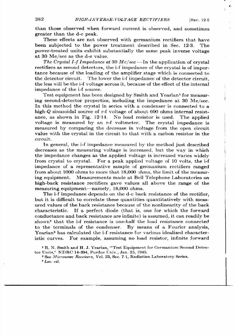
382 HIGH-INVERSE-VO TAGE REL’TIFIERIS
than those observed when forward cur ren t is observed,
grea t er than the d-c peak.
[SEC. 125
a nd somet imes
These effect s a re-no observed with german ium rect ifier s tha t have
been subject ed to the power t r ea tmen t descr ibed in Sec. 12.3. The
power -t rea ted un it s exhibit substan t ia lly t he same pea k in ver se volt age
a t 30 Me/see asthe d-c va lue.
Th e Cryst al Z-f Im pedance at 30 Me/ see —In t he applica tion of cr ysta l
rect ifiers as secon d det ect or s, t he i-f impeda nce of t he cryst al is of impor-
tance because of th loading of thear pl fie rstagewhich is connected t o
the detector circu it . Thelower the i-f impedance of the detect or circu it ,
th e less will be th e i-f volt age a cr oss it , becau se of t he effect of t he in terna l
impeda nce of th e i-f sou rce.
Test equipmen t has been designed by Smith and Year ian l for measu r-
ing second-detector proper t ies, including the impedance a t 30 Me/se .
In th is method the crysta l in ser ies with a condenser is connected to a
high -Q sinusoida l sou rce of r -f volt age of about 600 ohms in terna l resist -
ance, as shown in Fig. 12.14. No load resistor is used.
Th e a pplied
volt age is measured by an r-f voltmeter .
The crysta l impedance is
measured by compar ing the decrease in volt age from the open circu it
va lue with the cryst a l in the cir cu it t o tha t with a ca rbon resist r in the
circuit,
In genera l, t he i-f impedance measured by the method just descr ibed
decreases as the measu r ing volt age is increased, but the way in which
the impedance changes as the applie volt age is increased var ies widely
from crysta l to crysta l. For a peak applied voltage of 10 volt s, t he i-f
impedance of a represen ta t ive sample of german ium rect ifier s r anged
from abou t 1000 ohms to more tha t 18,000 ohms, the limit of the measu r-
ing equ ipmen t . Measurement s made at Bell Telephone Labora tor ies on
h igh-back resistance rect ifier s gave values a ll above the range of the
mea su rin g equ ipmen t—namely, 18,000 ohms.
The i-f impedance depends on the d-c back resist ance of the rect ifier ,
bu t it is difficu lt t o cor rela t e these quant it ies quant ita t ively with meas-
u red values of the back resistance because of the nonlinea r ity of the bac
character ist ic. If a per fect diode (tha t is, one for wh ich the forward
con du ct ance a nd back resista nce a re infin ite) is assumed, it can readily be
shownz tha t the i-f re istance is one-ha lf the load resist ance connected
to the termina ls of the condenser .
By means of a Four ier analysis,
Yea ria n3 h as ca lcu la ted t he i-f r esist an ce for va riou s idea lized ch ar act er -
ist ic curves. For example, assuming no load resistor , in fin ite forward
1R. N. Smith a nd H. J . Yearian , “Test E qu ipm en t for Germa nium Secon d Det ec-
t or Un it s,’ NDRC 14=394, P ur du e Un iv., J a n. 25, 1945.
2See Microwave Receivers, Vol. 23, %. 7.1, Ra dia tion La bor at or y Ser ies.
1Loc . m“f
I

SEC.
12,5]
HIGH-FREQUENCY PROPERTIES 383
con du ct an ce, an d con st ant back r esista nce, t he i-f resista nce is on e-t hird
the back resistance. With fin ite forward conductance the expression
for t he i-f r esist an ce becomes, t o a close a ppr oximat ion ,
(2)
where Rb is the constant back resistance and ~ is he rect ifica t ion effi-
ciency, which in this case will be very near ly equal to unity. As we have
seen , th actual crysta l rect ifier is ordinar ily far from linear in the back
direct ion and var ie grea t ly from crysta l to crysta l. Yearian concludes
from his analysis tha t where the back character ist ic has a very rapid
loowf
3
60
Cpsto
rectifier
FICI. 12. 15.—Impedan e test er for measur ing the impedance of crysta l secon d detect ors
a t 30 Me/see.
increase, or “ ta il,’’—as, for example, the region where the peak inverse
voltage is approached—the i-f resistance may be as low as one-eighth of
th average back resistanc obtained by taking the t ime average over the
i-f cycle of th e conducta nce in the back direct ion .
F igu re 12.15 sh ows t he cir cu it det ails for a n impeda nce t est er design ed
by the Purdue group for rout ine test ing of i-f impedance at 30 Me/see.
The detector circu it is the same as that shown in Fig. 12.14. A 6J 5 oscil-
la tor . dr ives th e 6AG7, which supplies the sinusoidal 30-Mc/sec v ltage
across the 600-ohm resistor . This voltage is measured by a vacuum-tube
voltmeter employing a 955 tube, with a high-impedance d-c meter to
measure its output . Standard voltages are chosen as 20 and 10 v lts
peak with no crysta l in place; these are adjusted by the HI and LO con -
t rols. The equipment is calibrated by means of standard carbon resistors
ranging from 20,000 to 500 ohms. The output inductance on the 6AG7
i.
I
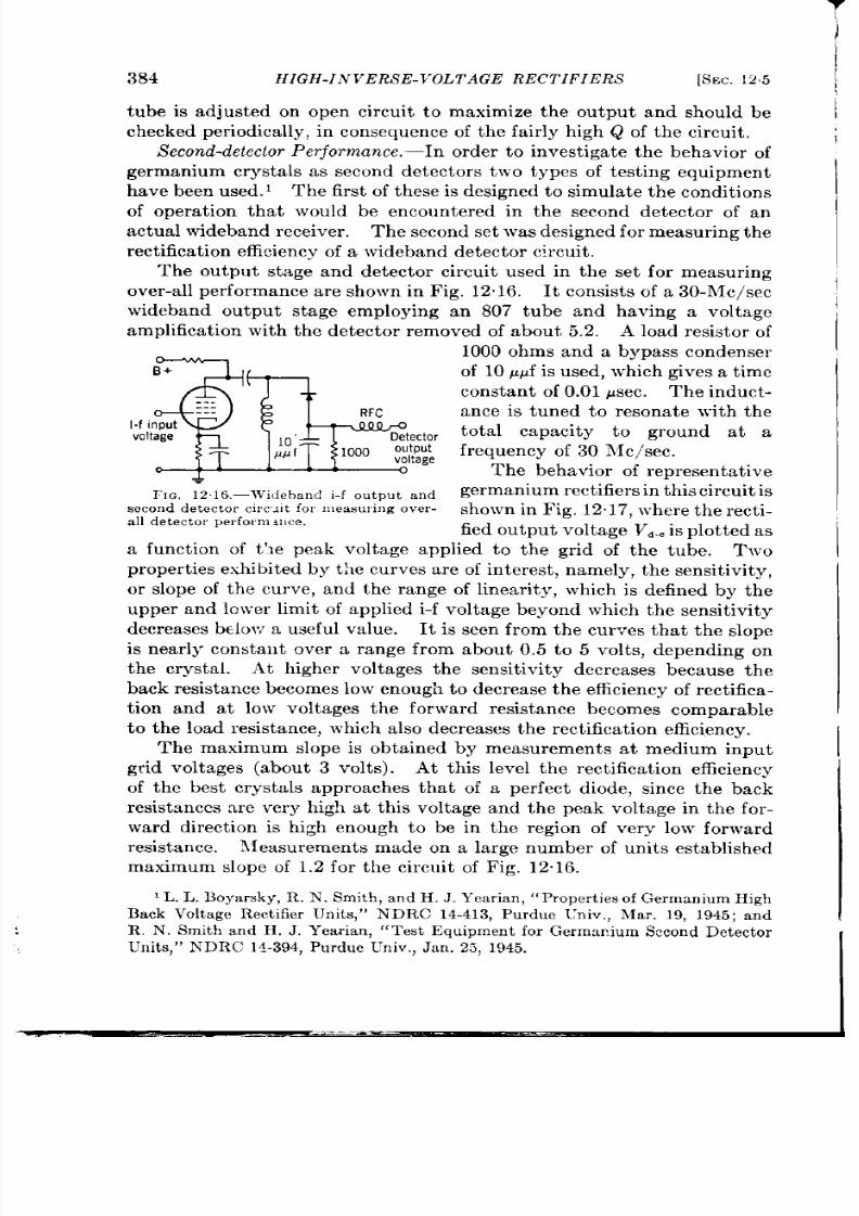
384
t ube is a dju st ed
HIGH-INVERS E-VOLTAGE RECTIFIERS
[SEC. 125
on open circu it to maximize the output and should be
ch ecked per iodica lly, in con sequ ence of t he fa ir ly high Q of t he circuit .
Second-detector Per formance.—In order to invest iga te the behavior of
germanium crysta ls as second detector s two types of test ing equipment
ha ve been used. 1 Th e first of th ese is design ed t o simula te th e condit ion
of opera t ion that wou ld be encoun tered in the second detector of an
actual wideba nd r eceiver . Th e secon d set was design ed for measur ing t he
r ect ifica tion efficien cy of a wideband det ect or cir cu it .
The ou tpu t st age and detector circuit used in the set for measur ing
over-a ll per form an ce a re shown in Fig. 12.16. It con sist s of a 30-Mc/sec
wideband output stage employing an 807 tube and having a voltage
amplifica t ion ith the detector removed of about , 5.2. A load re istor of
mlrn
1000 ohms and a bypass condenser
E+
of 10 ppf is used, which gives a t ime
con st an t of 0.01 ~sec.
The induct -
---
---
---
R C
an te is tuned to resona te with the
I. f Input
voltage
Detector total capacity to ground at a
10
p!-1
1000
,Olt age fr equ en cy of 30 Me/see.
utput
Th e beh avior of r epr esen ta tive
rlG, 1216.—Wi[lehand i-f output and
germanium r ect ifier s in t his cir cu it is
second detector cmc llt for Illeaau] mg over-
sh own in Fig. 12.17, wh er e t he r ect i-
all detector perform ~llce.
fied out put vo ta ge ~d.. is plot ted as
a funct ion of t ’le peak volt age applied to the gr id of the tube. Two
pr oper ties exh ibit ed by t he cu rves a re of in ter est , n am ely, t he sen sit ivit yy,
or slope of the curve, and the range of linearity, which is defined by the
upper and lower limit of applied i-f volta ge beyon d which t he sensit ivity
decr ea ses below a u sefu l va lu e.
It is seen from the curves tha t the slope
is nea r ly constant over a range from about 0.5 to 5 volts, depending on
t he cr yst al.
.kt h igher oltages the sensit ivity decreases because the
ba ck r esist an ce becomes low enou gh t o decr ea se t he efficien cy of r ect ifica -
t ion and at low voltages the forward resistance becomes comparable
t o t he loa d r esist an ce, wh ich a lso decr ea ses t he r ect ifica tion efficien cy.
gr id voltages (about 3 volts). At thk level the rect ifica t ion efficiency
of the best crysta ls approaches tha t of a per f ct diode, since the back
resistances me very high at th is voltage and the peak voltage in the for -
ward direct ion is h igh enough to be in the region of very low forward
resistance.
Afeasurements made on a large number of unit s established
maximum slope of 1.2 for the circuit of Fig. 12.16.
I
I
1 L. L. 130yarsky, R. N. Smith , and H. J . Year ian ,
“ Proper t ies of Germanium High
Back Voltage R ct ifier Unit s, ” NDRC 14-413, Purdue Univ., h fa r . 19, 1945; and
R. N. Smith and H. J . Year ian ,
“Test Equ ipment for Germar .ium Second Detector
Lln it s, ” NDRC 14-394, Purdue Univ., J an . 23, 1945.
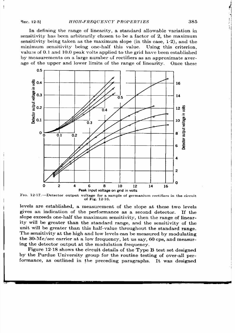
I
SEC. 125]
HIGH-FRE UENCY PROPERTIES
385
In defin ing the range of linear ity, a standard a llowable var ia t ion in
sensit ivity has been arbitra r ily chosen to be a factor of 2, the maximum
sensit ivity being taken as the maxim m slope (in th is case, 1.2), and the
minimum sensit ivity being one-half th is va lue. Using th is cr it er ion ,
va luw of 0.1 and 10.0 peak vo ts applied to the gr id have been established
by measurements on a large number of rect ifiers as an approximate aver-
age of the upper and lower limits of the range of linear ity. Once these
0.5
$ 0.4
16
,E
~ 0.3
14
>
5
~
: 0.2
12$
g
,s
$0.1
a
10 g
:
0
~
83
0
~
d
4
2
0
0 2 4 6 8 IO 12 14 16
Peak input voltageon grid in volts
FIG. 12. 17.—Detector ou tpu t voltage for a sample f germanium rect ifi r s in the circu it
of F ig. 12.16.
levels a re established, a measurement of the slope at these two levels
gives an indica t ion of the per formance as a second detector . If the
slope exceeds on eh alf t he maximum sen sit ivityy, th en t he r ange of linea r-
ity will be grea ter than th standard range, and the sensi ivity of the
unit will be grea ter than th is half-va lue th roughou t the standard range.
The sensit ivity a t the h igh and low levels can be measured by modula t ing
the 30-Mc/sec car r ier a t a low frequency, let us say, 00 cps, and measur-
ing the detector ou tpu t a t the modula t ion frequency.
Figure 12.18 shows the circu it deta ils of the Type B test set designed
by the Purdue University group for the rou ine test ing of over -a ll per -
formance, as ou t ined in the preceding paragraphs. It was esigned
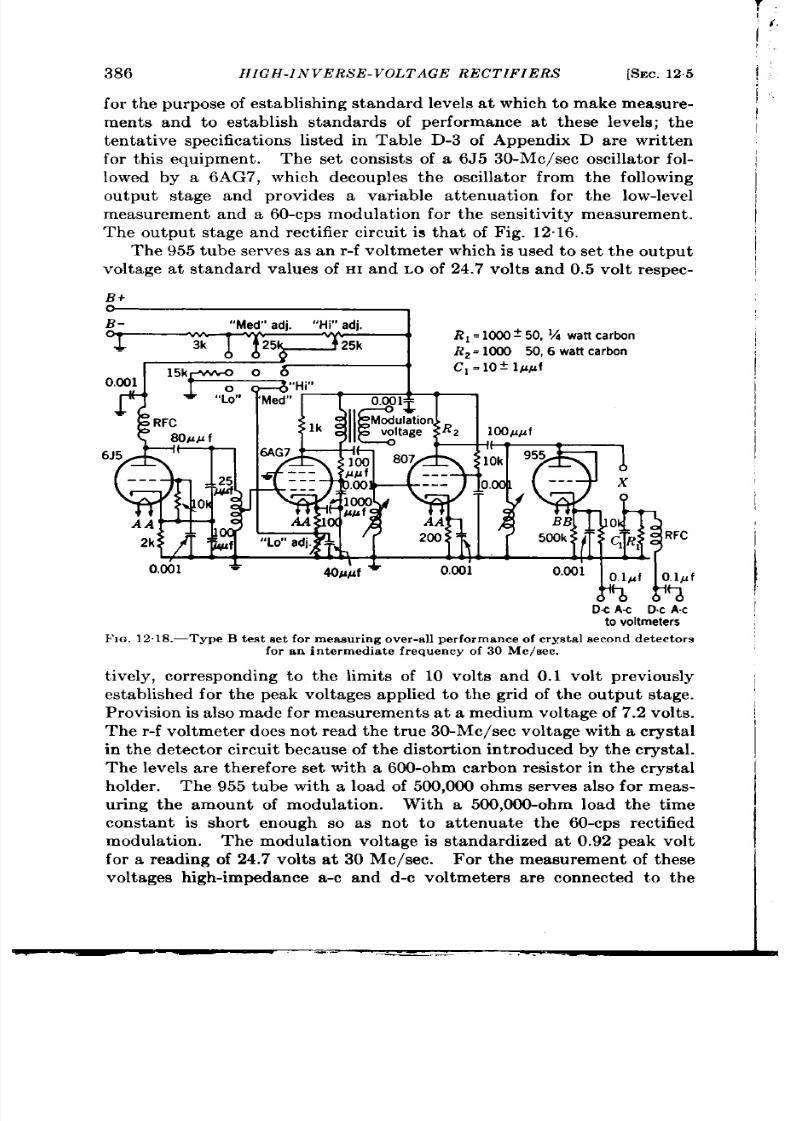
386
HIGH-IN VER S E- VOLT AGE R ECT IFIER S
[SEC.125
for the pu rpose of establishing standard levels at which to make measu e-
ments and to establish standards of per formance at these levels; the
tenta t ive specifica t ions listed in Table D-3 of Appendix D are writ ten
for th is equipment . The set consists of a 6J 5 30-Mc/sec oscilla tor fol-
lowed by a 6AG7, which decouples the oscilla tor from the following
output stage and provides a variable at tenuat ion for the low-level
m ea su remen t a nd a 60-cps mo u lat ion for t he sen sit ivityy m ea su rem en t.
The out u t stage and rect ifier circu it is tha t of Fig. 12.16.
The 955 tube serves as an r-f voltmeter which is used to set the outpu t
volt age at standard values of HI and LO of 24.7 volt s and 0.5 volt respec-
R+
f
DC A< Dc AC
t o
voltmeters
FIG, 12,
18.—Type B test aet for mea eu rin g over -a ll per forman ce of cr yst al s econ d d et ect or s
for an in termedia te frequ en cy of 30 Mc/6ec.
t ively, cor responding to the limits of 10 volt s and 0.1 volt previously
established for the peak voltages applied to the gr id of the output stage.
P rovision is also made for measurements at a medium voltage of 7.2 volt s.
The r-f voltmeter does not read the t rue 30-Mc/s c voltage with a crysta l
in the det ector circu it because of th distor t ion in t rodu ced by the crysta l.
The levels are therefore set with a 600-ohm carbon resistor in the crysta l
holder . The 955 tube with a load of 500,000 ohms serves a lso for meas-
ur ing the amount of modula t ion.
With a 500,000-ohm load the t ime
constant is shor t enough so as not to a t tenuate the 60-cps rect ified
modulat ion . The modula t ion voltage is standardized at 0.92 peak volt
for a reading of 24.7 volt s at 30 Me/see. For the measurement of these
voltages high-impedance a-c and d-c voltmeters are connected to the
I
I

I
SEC. 125]
HIGH-FREQUEN CY PROPERTIES 387
appropr ia te ou t put terminals o the 955 detector circu it .
The same
meters are switched to the crysta l output terminals for the test measure-
ments. The var iable inductance in the output circu it of the 807 is
tuned to give maximum output voltage with a GoO-ohm resistor in the
crysta l holder . This corresponds closely to the adjustment for maximum
output with a good germanium detector in place.
The modula t ion method is sa t isfactory for measur ing sensit ivity at
h igh and medium levels but is impract ical a t low level. At low level,
exper imen ts show good correla t ion between sensit ivity and d-c output
voltage for a iven type of rect ifier ; a the standard low-level input ,
35 mv d-c output corresponds to a slope of about one-ha lf the maximum
value at medium levels. To calibrate the output of the 807 for the
low-level test , standard crysta ls are used which have been checked
against pr imary standards mainta ined at the standards labora tory; the
955 voltmeter is inadequate a t this voltage level. The crysta l output
volt age is mea su red wit h a 20,000-ohm millivoltmet er .
Measurements have been made at u rdue University 1 on repre-
senta t ive samples of power-t rea ted units having very high back resist -
ances; these units had been made at Purdue and at the Bell Telephone
Labora tor ies. With the h gh-level 30-Mc/sec input (24.7 volts) the d-c
output voltages average about 10 volts, with variat ions of not more
than a volt or so fr m crysta l to crystal. The 60-cps modula t ion output
voltage varies from about 0.3 to 0.4 volt .
Wit h t he low-level 30-Mc/s ec
input voltage, the d-c output voltage is more than 40 mv for the Bell
Telephone Labora tor ies units and somewhat lower for the Purdue units.
A comparison of these results with those for rect ifiers tha t have not been
subjected to power t rea tment shows tha t the power t rea tment causes an
increase in the high-level output volta e of th e detector , especia lly in th e
a-c output voltage where the increase is by a factor of about two.
This
fact implies that the range of linear ity of the response has been extended
to considerably higher input levels by the power t rea tment . At low
level the Bell Telephone Labora tor ies power t rea tment also causes a
significant increase i the a-c output voltage, but the somewhat more
dra st ic power t rea tm en t u sed in man ufactu ring t he P ur du e cr ysta ls cau ses
a small decrease of sensit ivity at this level. Result s obtained with a
sample of germanium crysta ls made by Sylvania Elect r ica l Products
Company are comparable to those obta ined for the Purdue hea t-t rea ted
units.
It is evident from these result s that the power trea tment , which
impr oves t he d-c pr oper ties, a lso impr oves second-det ect or per formance.
I L . Boyarsky, P. B. Picker , A. W. McDonald, R. N. Smith , R. M. Whaley, and
H . J . Yea ria n, “P rodu ct ion a nd P er forma nce of Germa nium H igh Ba ck Volt age, H igh
Back Res is ta n ce Crys ta l Rect ifier s, ”
NDRC 14577, P ur du e Un iv., Oct . 31, 1945.
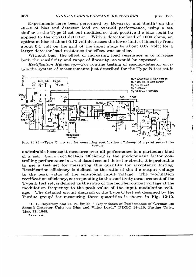
388
HIGH-INVERSE-VOLTAGE RECTIFIERS
[SEC.
125
Exper iments have been per formed by Boyarsky and Smithl on the
effect of bias and detector load on over all performance, using a set
similar to the Type B set but modified so that posit ive d-c bias cou ld be
applied t o t he cr yst al det ect or .
With a detector load of 1000 ohms, an
opt imum bias of about 0.12 volt decr ea ses th e lower limit of linear ity fr om
about 0.1 volt on the gr id of the input stage to about 0.07 volt ; for a
la rger det ect or loa d r esist an ce t he effect wa s sma ller .
Without bias, the effect of increasing load resistance is to increase
both the sensit ivity and range of linear ity, as would be expect d.
Rectification E$cien cy.—For r out in e t est in g of secon d-det ector cr ys-
ta ls the system of measurements just descr ibed for the Type B test set is
FIG. 12. 19.—Type C test set for measur ing r ect ifica t ion efficien cy of crysta l second de-
tectors.
u ndesir able beca use it m ea su res over -a ll per forma nce in a pa rt icu la r kin d
of a set . Since rect ifica t ion efficiency is the predominan t factor con-
t rollin g per formance in a wideba nd second-det ect or cir cu it , it is pr efer able
to use a test set for measur ing this quant ity for acceptance test ing.
Rect ifica t ion efficiency is defined as the ra t io of the d-c ou tput voltage
to the peak value of the sinusoidal input voltage. The modulat ion
r ect ifica t ion efficien cy, cor r es ponding t o t h e sen sit ivit y mea su r emen t of t h e
Type B test set , is defi ed as the ra t io of the rect ifier output voltage at the
modulat ion frequency to the peak value of the input modulat ion volt -
age. The deta iled circu it diagram of the Type C test set designed by the
Purdue group’ for measur ing these quant it ies is shown in Fig. 12”19.
IL. L. Boyarsky and R. N. Smith ,
“Depen den ce of P er forma nce f Germa nium
Second Detector Units on Bias and Video Load,” NDRC 14-416, Purdue Univ.,
Mar . 28, 1945.
s Lot . cit.
i

SEC. 126]
S ILICON HIGH-INVERSE-VOLTAGE RECTIFIERS
389
The 6J 5 and 6AG7 tubes serve the same purpose as in the Type B test set .
A push-pull amplifier employing an 829B tube delivers 30-volt peak
sinusoida l voltage a t a frequency of 30 Me/see to the 100-ohm load Rs.
The t ransformers T, and Ts are cr i ica lly coupled, tuned-pr imary and
tuned-seconda ry t r ansformers .
The in terna l impedance of t he r -f sou rce
across
Ri
is 50 ohms. The detector ou tpu t circu it consist s of a 10-p~f
con den ser an d a 1000-ohm loa d r esist or a s in t he pr eviou sly descr ibed set .
The 955 r-f voltmeter is the same as tha t in the Type B test set except
tha t a l ad resistor of 600,000 ohms is used instead of on e of 500,000 ohms.
F or h igh-level measu remen ts, th e HI con tr ol is adju sted for a readin g
of 29.1 volt s on the d-c meter of the r -f voltmeter , with a 750-ohm carbon
r esist or in t he cr yst al h older .
Th e 60-cps modu la tion volt age is a dju st ed
for a reading of 0.50 volt on a high-impedance a-c meter connected to the
a-c terminals of th e r -f voltmeter
The carbon resistor is now replaced
by the crysta l to be tested and the a -c and d-c voltmeter s switched to the
“X” terminals
The d-c ou tput voltage divided by 29.1 gives the
rect ifica t ion efficiency and the a-c ou tpu t volt age mult iplied by 2 gives
t h e modu la t ion r ect ifica t ion efficiency.
The r-f peak voltage for “medium level” is standardized at 9.o
volt s, and the low level is set by means of standard crysta ls as in the
Type B test set .
The theoret ica l maximum value for the modula t ion rect ifica t ion
efficiency is about 41 per cen t for both the high and medium levels; the
value corresponding to one-ha lf maximum sensit ivity in the over-a ll
measuremen t is about 25 per cen t .
.4 va lue of 35 mv for the low-level
ou tpu t volt age cor respon ds t o a bou t on e-h alf ma ximum sen sit ivityy.
12.6. Silicon High-inverse-voltage Rect ifiers.-Following the dis-
cover y of th e high-in verse-volta ge proper t y in appropr ia tely doped ger-
manium an explora tory invest iga t ion was car r ied ou t on silicon by the
crysta l group at the University of Pennsylvani . 1
Ingots were prepa red from high-purity du Pen t silicon , to which were
added small known amounts o va rious impurit i s. The ingots were
made in a vacuum furnace in quartz crucibles. As in the case of mixer
crysta ls, t he addit ion of 0.02 per cen t of beryllium insured a solid ingot
free from cracks. The beryllium did not appear to have much effect
on t he elect rica l pr oper ties of t he silicon .
The prepara t ion of the su rface was similar to tha t used for silicon
mixer crysta ls. The ingot is sawed in to wafer s about 1 mm thick. One
side is n ickel-pla ted for solder ing to th e car tr idge stud, and t he ot her side
is fir st wet -ground with 600 Carborundum, then polished to a high gloss
on 0000 emery paper wet with kerosene. It is then hea t -t r ea t ed in a ir
1 M. N. Lewis, J . H. Taylor , R. J . Gibson, J r., and W. E. Stephens, “High Back
Volt age Silicon ,” NDRC 14-453, Un iv. of P en n., J u ne 28, 194 .
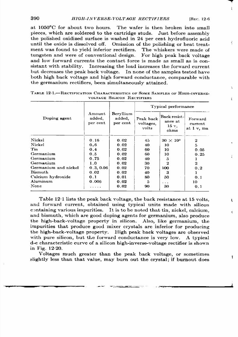
390
HIGH-INVERSE-VOLTAGE RECTIFIERS [SEC. 126
at 105O”C
for about two hours. The wafer is then broken in to small
pieces, which a re soldered to the ca r t r idge studs. J ust before assembly
the polished oxidi ed sur face is washed in 24 per cen t hydrofluor ic acid
until theoxide is dissolved off. Omission of thepolish ing or heat t r ea t -
men t was fou nd t o yield in fer ior r ect ifiers.
Thewhiskers were made of
tungsten and were of conven t iona l design . For h igh peak back voltage
and low forward curren t s the con tac force is made as small as is con-
sisten t with stability. Increasing the load increases the forward cur ren t
but decr ea ses t he pea k ba ck volta ge.
In none of the samples tested have
both high back volt age and high forward conductance, comparable with
t he germa nium r ect ifier s, been sim ulta neou s y a tt ain ed.
TABLE12.1.—RECTIFICATIONHARACTERISTICSFSOMESAMPLESFHIaH-INVERSE-
VOLTAGE SILICON RECTIFIERS
Dopin g a gen t
Nickel
Nickel
Tin
Germanium
Germanium
Germanium
German ium and n ick el
Bismuth
Calcium hydroxide
Aluminum
Yone
Amount
added,
p er cen t
0.16
0.6
0.4
0.5
0.75
1,0
0.3,0.06
0.02
0.1
0.006
Beryllium
added,
per cen t
0.02
0.02
0.02
0.02
0.02
0.02
0,02
0.02
0.01
0.02
0.02
Typica l per f rmance
Peak back
voltages,
volts
45
40
60
60
40
30
70
40
so
5
90
lack resis t -
a nce a t
15 v,
ohms
30 x 103
10
10
5
2
lIM
3
50
.
30
Forward
current
it 1 v, ma
2
5
0.05
0.25
1
2
0.2
1
0.1
10
0,1
Table 12.1 lists the peak back vo tage, the back resistance a t 15 volts,
and forw rd curren t , obta ined using typica l units made with silicon
c Onta in ing var ious . impur it ies.
It is to be noted that t in , n ickel, ca lcium,
and bismuth , which are good doping agen ts for germanium, a lso produce
the h igh-back-voltage proper ty in silicon . Also, like germanium, the
impur it ies tha t produce good mixer crysta ls a re in fer ior for producing
the high-back-voltage proper ty. High peak back voltages a re observed
with pure silicon, but t l,e forward conductance is very low. A typica l
d-c ch ar act er ist ic cu rve of a silicon h igh -in ver se-volt age r ect ifier is sh own
in F ig. 12.20.
Voltages much grea ter than the peak back voltage, or somet imes
slight ly less than tha t va lue, may b rn ou t the rysta l; if burnou t does

SEC. 12.7]
NEGATIVE-RES IS TANCE CHARACTERIS T ICS 391
not occ r , the applica t ion of the peak back voltage tends to reduce
hysteresis effects. Ingenera l, thehigh -back-vol age silicon made by the
Pennsylvania group is not comparable with germanium in ability to
wit h st and power dissip at ion .
Tests made of the second-detector proper t ies of a typica l group of
rect ifiers sh owed tha t th ey will pass all t he requ irements of the tenta t ive
specifica t ions listed in Appendix D, except t he low-level rect ifica t ion;
however , they area lso in ferior to the germanium rect ifier in high-level
r ect ifica tion and sen sit ivit y.
It must be remembered, however , tha t
much less work has been done on high-back-voltage silicon than on
germanium and it is possible tha t a comparable amount f resea rch on
silicon may a lt er t his sit ua tion .
F or th eh igh -ba ck-volt age silicon r ect ifier s, m ea su remen ts wer emade
of the rect ified current as a funct ion of frequency, similar to the exper i-
ments on germanium. In these exper iments the shor t -circu ited rect ified
current was measured for 1 volt rms applied to the crysta l a t frequencies
-“4°
II&12.20.—Typical char acteristic curve of a silicon high-inverse-voltage rectifier.
of 60 cps and 30 Me/see. The rect ified curren ts for th samples tested
were rela t ively small, ranging from 0.1 to 0.7 ma, but the decrease in
rect ified current over the frequency range from 60 cps to 30 Me/see was
less than 10 per cen . It can be seen , by reference to Fig. 12”11, tha t the
high-back-voltage silicon units a re much less f equency-sen sit ive than
the german ium rect ifier s.
12.7. Th eory of the Negat ive-resistance Character ist ics.-There is as
yet no sa t isfactory theory of the high inverse voltages and negat ive-
resistance character ist ics displayed by the crysta ls discussed in th is
chapter.
A theory has been developed by Benzer l that a t tempts to account
for the existence of voltage peaks and negat ive re istance on the basis
of the on set of int r insic conduct ion at th e high con t ct tempera tu res tha t
must exist a t the peak voltage and in the negat ive-resistance par t of the
characteristic.
Although there is lit t le doubt that tempera ture effects
are responsible and tha t int r insic conduct ion has a bear ing on the prob-
1 ,
[
1S. Benzer,
“The High Voltage Ger manium Rectifier ,” NDRC 14.375, Purdue
Univ., Dec. 26, 1944.
392
HIGH-INVERS E-VOLTAGE RECTIFIERS
[SEC.
128
lem, it can be shown tha t Benzer ’s t heory is inadequa te because of the
in compa tibilit y of h ls post ula tes.
A more precise analysis, made by
H. C. Tor rey,’ revea ls tha t volt age peaks cannot possibly exist (in the
\
forward direct ion , a t least ) if the thermal conduct ion of the whisker is
n eglect ed, a s it is in Ben zer ’s t heor y.
Th is n eglect seem s ver y pla usible,
however , in the case wher e thermal equilibr ium is established a ft er a few
secon ds of con tin uou s cu rr en t flow.
Some numer ica l ca lcu la t ions by Goodman’ indica te tha t voltage
peak may pe haps occur if t he thermal resist ance of the whisker is taken
in to accoun t , but more work needs to be done before the theory can be
cons idered adequa te.
Perha ps th e most puzzlin g quest ion is h ow it , is possible for th e ba rr ier
to withstand the enormous field in tensit ies tha t must exist a t peak
voltages of 100 vo t s or more. Breakdown by bar r ier -lower ing ar ising
from image forces and tunnel effect s would be expected for a bar r ier of
norma th ickness (10–6 or 10–5 cm) at only a few inver se volt s. W. E.
St eph en s3 h as post ula ted a ba rr ier a s t hick a s 10–4 cm for t he h igh -in ver se-
volt age rect ifier s, bu t it is difficu lt t o see h ow such a t hick ba rr ier could be
formed.
12.8. Ph ot oelect ric Effects in Silicon and Germanium.-In t he cou rse
of r esea rch on cr yst al r ect ifier s in ter est in g ph ot oeffect s wer e obser ved in
,
both silicon and germanium. These effects a re rela t ed to the rect ifying
cha racte ist ics of the semiconductor and will undoubtedly cont r ibute to
t h e under st anding of s em iconduct ion .
In addit ion they hold promise for
p ract ica l photoe lect r ic applica t ions.
Photoelectric Effects in Silicon .—The photoconduct ivity of pu re du
Pen t silicon was observed a t the Radia t ion Labora tory by M. Fox and
C. S. Pea rsa 114du rin g t he developm en t wor k on m ixer cr yst als r epor ted in
Chap. 10. A deta iled invest iga t ion of the eff ct was not m de at tha t
t ime, however . More recen t ly Miller and Greenbla t t5 have repor t ed an
explora tory invest iga t e on of photoeffect s in pure silicon . The samples
invest iga ted wer e pure du Pen t silicon needles or melt s made from these
[
n eedles. Both phot ocon duct ive and ph ot ovolta ic effect s wer e obser ved.
Samples were pla ted, soldered on to a mount , and a poin t con tact made
‘1
with a tungsten whi ker . Whiskers of molybdenum and pla t inum were
a lso used, but the whisker mater ia l was found to have lit t le in fluence on
t he ch ar act er of t he ph ot oeffect .
1Unpublished dat a .
2 P r iva te communica tion fr om B. Goodman .
i Unpublis hed dat a .
4Unpublished dat a .
5 P. H. Miller , J r. and M. H. Greenbla t t , “ hotoeffect s in Pure Silicon , ” hTDRC
!
14-412, U niv. of P en n., Ma r. 20, 1945,
SEC. 128]
PHOTOELECTRIC EFFECTS IN S ILICON
393
In t he ph ot o on du ct ive effe t t he ch an ge in cu rr en t u pon illumin ation
of the con tact a rea ~vas invest iga ted as a funct ion of wavelength and
in tens ity of illumina t ion .
Most of th e samples in vest iga ted wer e p-type
m ater ia l, and t he la rgest ph ot ocon du ct ive effect s wer e observed with t he
poin t posit ive. In the spect ra l-dist r ibut ion curve, the maximum
r espon se occu rs a t a }va velen gt h of a bou t 1.5 p, wit h a n a ppa ren t t hr esh old
a t abou t 2.1 p. The wavelength at which the maximum occu rs is inde-
penden t of the silicon, the poin t ma ter ia l, and the bias voltage, but the
change in cu r ren t upon illuminat ion increases as he bias volt age is
increased.
Occasiona l t ime-dependen t effect s wer e observed. After the in it ia l
increase in cur ren t when the light is tu rned on , th e cu r ren t may con t inue
to increase for severa l seconds. When the light is tu rned off, th ere is a
sudden decrease, which may be followed by a gradua l fa lling-off in the
cur ren t . Such effect s a re difficu lt to duplica te and are usually found
wit h mech an ica lly u nst able con ta ct s.
No change in cu rren t as la rge as 0.5 per cen t was observed with doped
mater ia ls, a lthough in pu re mater ia ls a change in conduct ivity as l rge
as a factor of 10 was observed. Only the region in the neighborhood of
t he poin t con ta ct wa s ph ot ocon du ct ive.
The increase in cur ren t produced by an increase of in tensity of
illumin ation was in vest iga ted, an in ca ndescen t lamp bein g u sed as a light
source. For low in tensit ies the increase in cur ren t is approximately
pr opor tion al t o t he ligh t in ten sit y; as t he illumin ation is fu rt her in cr ea sed,
the cur ren t increase is less rapid than linear .
Th e invest iga tion of t he ph otovolta ic effect in silicon sh owed th at th e
region as far as severa l millimeters from the poin t con tact can be the
photosensit i e elemen t . The shape of the spect ra l-dist r ibut ion cu rves
a re similar to those obta ined in th e photocon du ct ive effect , with a maxi-
mum at the same wavelength . The cur ren t is usua lly in the direct ion of
h igh r esist an ce, a lt hou gh occa sion ally cu rr en ts in t he oppos t e d r ect ion
a re found. In a typica l sample with zero bias a cur ren t of 0.16 ~a was
observed for an illumina t ion of 1.2 X 10⁻² wat ts/cm2 at a wavelength d
1.5 p, the maximum of the spect ra l-dist r ibu t ion curve. The silicon , when
illuminated, acts as a cell having constan t in terna l resist ance and an emf
tha t depends upon the wavelength and in tensity of illuminat ion . The
in terna l resistance appea rs to be rough ly th ree t imes the spreading
resistance.
All the exper imen ts descr ibed in the preceding paragraphs were on
u nt rea ted su rfa ces of crysta ls.
P~otoeffects are still observed on pol-
ished surfaces bu t appea r to be so complica ted and difficu lt to reprodu ce
tha t they have not as yet been studied in deta il.
Photoelectric E ffects in Germanium. —Ph t oeffect s in germanium h igh -

394
HIGH-INVERSE-VOLTAGE RECTIFIERS
[SEC. 12.8
back-voltage rectifiers were first observed
by P. R. Bell a t the Radia t ion
Labora tory and led to a deta iled study by Benzer l of photoeffect s in
germa nium; t hese stu dies a re summa rized in t he followin g pa ra gra ph s.
P hotoeffects a re commonly found in high-resist ivity germanium and
occur mos frequen t ly in the boundary region separa t ing p-type and
+ 0.4 -
+ 0.3-
2
.E
z+o.2-
:
d
+0.1 -
-5 -4 -3 -2 -1 0
a
A plied voltage in volts
- OJ 1
FIG. 12.2 1.—D-c ch ara cter ist ic of a germanium ‘‘ p hotodiode” cryst al at 25°C, no illumi-
nation.
+40-
+30-
;
c
-
+20-
~
:
z
+lo-
-3 -2 -1
+1
+2
+3
+4
Appliedwitage m volts
-1o-
Fm. 12.22 .—D-c characteristic f a germanium “ photopeak” crystal at 25”C, no illumi-
nation.
n-type germanium. Th e photosen sit ivity is associa ted with t wo unusual
types of cu rrent -voltage character ist ic or a combinat ion of these two
types. The fir st type, illust rated in Fig. 12.21, shows a sa tura t ion effect
in the forward curren t ; it has been given the descr ipt ive name of “ phot~
diode.”
The second type, shown in Fig. 12.22, exhibits a volt age peak
followed b a n ega tive-r esist an ce r egion , wh ich becomes posit ive a t la rger
I S. Ben zer ,
“The High Back Volt age German ium Rect ifier ,” NDRC 14-342,
Pu rdue Univ., Nov. 1, 1944; and “Photoelect r ic E ffect s in Gernumium,” NDRC
14-5S0,PurdueUniv., Oct. 31, 1945.

SEC. 12.8]
PHOTOELECTRIC EFFECTS IN S ILICO
395
currents .
With il umination the peak voltage decreases and may be
reduced to pract ica lly zero if the illuminat ion is su fficient ly in tense.
This type haa been given the name “ photopeak.”
F@e 12”23 shows the effect of var ious in tensit ies of white light
upon the forward character ist ic of a photodiode. The back character -
ist ic is lit t le a ffected. The effect is rever sible and occu rs f r fla shes as
shor t as 10–5 sec. It can be seen from Fig. 12”23 tha t the photocur ren t
is a lmost independen t of the voltage applied to the rect ifying con tact in
the sa tura t ion region . The photocu r ren t is a lso propor t iona l to the
in tensit y of illumin ation over a wide ra nge.
For a good photodiode th is
linear response extends up to illuminat ions of 1 or 2 lumens/cm2. Spec-
t ra l-dist r ibu t ion cu rves show a
maximum response at a wave-
length of abou t 1.3 p, with a
th reshold of abou t 1.6 p. The
number of photoelect rons per
in ciden t qu an tum a t t he m aximum
is about 0.9.
Photodiode poin ts a re a lso
photovolt a ic. A given crysta l
genera tes an emf propor t iona l to
t he in ten sit y of illumin at ion , wit h
an in terna l resistance equal to th e
12 -
0.9 lumens/cm2
1.0 -
e
& 0.0 -
0.6 lumens/ mz
~ 0.6 -
3
0.3
lumens lcrn2
0.4 -:
02 -
0
slope of t he ch ar act er ist ic cu rve a t
the or igin .
Thk resistance is,
in genera l, la rge bu t , by increas-
ing the con tact a rea it may be
-.
012345
Appliedoltsge n wi t s
F IQ. 1223.-E ffect of wh it e-ligh t illumin a-
t ion on photodiode character is t ic.
grea t ly reduced withou t ffect ing the photoelect r ic proper t ies. The
pola r ity is such tha t the whisker becomes nega t ive. The spect ra l-
dist r ibut ion cu rve is th e same as tha t for th e ph otoconduct ive effect .
The sa tura t ion cu rren t of a photodiode is ext remely sensit ive to
tempera tu re. At room tempera tu re a change f 10”C changes the sa tura -
t ion cur ren t by a factor of 2.
Th ese ph ot odiode ch ara cter ist ics occu r in r egion s tha t m ay be severa l
square millimeters in a rea Such a region may be made visible by etch -
in g t h e su r fa ce elect rolyt ica lly.
All poin ts with in a given region have
r emar ka b y sim ila r ch ar act er ist ics.
With in th is region , a change in
wh kk er for ce pr odu ces la rge ch an ges in back r esista nce while t he for wa rd
sa tu ra tion cu rr en t is a lm ost u na ffect ed.
When volt age is applied in the
sa tu ra tion dir ect ion , a la rge pot en tia l dr op is fou nd a cr oss t he bou nda ries
of the region . With the applied voltage in the back direct ion , however ,
the drop ;cross the boundary is much l&s. These effect s a re in terpreted
f
1
,
by Benzer to mean tha t the photodiode effect is caused by a la rge barr ier
:
396
HIGH-IN VERS E- l“OLTAGE RECTIFIERS
sur rounding the sensit ive su r face element , thus limit ng
curren t for any poin t con tact made with in the region ,
Th 6
[SEC. 12.8
th e for war d
ba rr ier must
be a rect ifying one, since the back curren t , with la rge whisker forces, fa r
exceeds t he sa tu ra tion cu rr en t.
Benzer found tha t , if a small spot of light is moved along a line
in ter sect in g t he sen sit ive r egion , t he ph ot ocu rr en t r ises r apidly t o a m axi-
mum at the boundary of the sensit ive region , then passes th rough a
sha llow min imum
as the region is
traversed.
He in terprets th is resu lt
to mean tha t the barr ier , even in the cen ter of the reg on, lies very close
t o t he su rfa ce.
Th e “ ph ot opea k” type of ch aracter ist ic was repor ted by lVoodya rd,’
who used the negat ive-resistance region to produce oscilla t ions up to
frequencies as high as 1 31c/sec.
Benzer repor t s2 tha t photopeak
ch ar a ct er ist ics wit h peak volt a ge
as
high as 25 volt s h ave been observed,
a lthough pea!w are usually found at 1 or 2 volt s.
Th e cu rr en t at the
peak is usualljr of the order of 1 ma.
At cur ren ts well above 1 ma and
fiba ve t he n ega tive-ch a ra ct er ist ic r egion , t h e ch ar a ct er ist ic is det erm in ed
by the spreading resistance.
For very h igh-resist ivity mater ia l, t he
spreading resistance may be so large tha t the photopeak appears only
as a kink in th e ch aracter ist ic.
Photopeaks a re usually found in border regions between p-type and
n -t ype m ateria l, bu t the ph ot opea k r eg on usu ally h as a lin ea r dim en sion
of on ly a fr act ion of a m illimet er .
Unlik e t he ph ot odiode, t he ph ot opea k
may vary grea t ly from one poin t to another , and it is very sensit ive to
whisker pressu re; the peak voltage decreases as the whisker load is
increased.
It has a lready been ment ioned tha t the peak voltage decr ases with
illumination.
At low intensit ies of illuminat ion the decrease in peak
volt age is pr opor tion al t o in ten sit y.
Sen sit ivit y va ries gr ea tly fr om on e
unit to an other ; an illuminat ion of 0.5 lumen/cm2 is suffi ien t to r em ove
completely the peak of a sensit ive unit , whereas an insensit ive one may
show lit t le response. Explora t ion with a small spot of light shows tha t
only light tha t falls in the immedia te region of the poin t is effect ive.
A ph ot o respon se may be obta ined for light flashes as sh or t as 10–5 sec.
Th e spectr al-dist ribu tion cu rve h as n ot been st udi d in deta il, but pr elim -
inary exper iment indica te tha t it is similar to tha t of the photodiode.
The photopeak rect ifier has a possible applica t ion as a t r igger ing
device.
If it is bia sed posit ively ju st below t he pea k volt age, illumin at ion
will cause he peak to decrease so tha t the cur rent jumps to a value
] J . R. Woodya rd,
“ Not es on Cr yst al Det ect or s, ” Sper ry Resea rch La bor at or ies
I iepor t 5220-110, Ap r. 6, 1943,
z S . Ben zer ,
“ The,J Iigh Back Voltage Germ anium Rect ifier , ” NDRC 14-342,
P ur du e Un iv., Nov. 1, 1944,
SEC. 128]
PHOTOELECTRIC EFFECTS IN S LICON
397
limited by the spreading and circuit resistances, a cu rrent la rge enough
to actua te a relay. Since the crysta l rect ifies, an a-c bias can be used;
the device then is automat ica lly restored to opera t ing con it ion when the
ligh t is r emoved.
Like the photodiode, the photopeak is tempera tu e-sensit ive, the
peak voltage decreasing with increasing tempera ture. Raising the
tempera tu re from 24° to 50°C will, in genera l, reduce the peak voltage by
a factor of about two. Photopeak crysta ls a re not as rugged as photo-
diode crysta ls and may be burned out by the passage of too much current
t hr ou gh t he con ta ct .
Th e ph ot oeffect men tion ed ea rlier as obser ved in some h igh -in ver se-
voltage germanium rect ifiers is of a clifferent na ture from those just
descr ibed. In th is effect , illuminat ion causes changes in current a t a
given applied voltage, as well as a photovolta ic effect when there is no
applied voltage. Athlghback voltage, t ime lags occur in the responses,
and the current dur ing illuminat ion may beless than tha t in the dark.
In addit ion to these effects, many in terest ing combinat ions of the
types just discussed have been observed. Fur ther research work on these
effects wi l undoubtedly shed fur th er light on the t heor y of semiconduc-
t ion and the nature of the high-back-voltage phenomenon. On the
pract ical side, the photopeak and photodiode crysta ls offer excellen t
pr ospect s for t he developmen t of phot oelect ric cells u sin g t hese mat er ia ls.
t
CHAPTER 13
WELDED-CONTACT GERMANIUM CRYSTALS
It has long been supposed tha t a sim le con tact r ct ifier used as a
frequency conver t er must a lways have a conver sion loss grea t er than
unity, or , in other words, tha t the ava ilable ou tput (i-f) power must
a lways be less than the available input (signa l) power .
This specious .
con ject ur e ha s n o con vin cin g t heor et ica l a rgumen t in it s fa vor , h owever .
N-or th , of the Genera l Elect r ic Company, has recen t ly demonst r a ted’ .
tha t the conjecture is, in fact , fa lse. Nor th has const ructed germanium
rect ifiers with welded cont acts that have th e remar kable pr oper ty (un der
cer ta in bias and r-f tuning condit ions) of deliver ing mor e power a t in ter -
media te frequency than is available from the signal sou rce.
Energy
conserva t ion is of cou rse not viola ted since the loca l oscilla tor supplies
t he
extra power .
It has been shown tha t this amplifying ability of Nor th’s crysta ls is
a ssocia ted (a lt hou gh n ot n ecessa rily con com it an t) wit h t he ph en om en on
of negat ive i-f conductance which they somet imes exhibit . There is
I
convincing evidence tha t nega t ive i-f conductance is a resu lt of two
factor s: (1) the var iability of con tact capacitance with volt age (a proper ty ‘
a lso of n orma l r ect ifier s) a nd (2) t he a bn orma lly low spr ea din g r esist an ce.
LTnfor tuna tely, measurements have shown tha t , because of th e grea t
amount of i-f noise power they genera te, t hese remarkable crysta ls a re,
when ju dged by over-a ll r eceiver noise f gure, infer ior t o standard t ypes
in spite of their amplifying proper t ies. The crysta ls can be used in
such a manner , however , tha t their i-f conductance is posithe. In th is
condit ion they behave as normal crysta ls; t hei loss, a lthough small, is
grea t er than one and their noise is not excessively la rge. Used in th is
way they are comparable to the best of the standard conver t er types.
Th ey a re su per ior t o all st anda rd t ypes aa h armon ic gen er at or s, especia l y
t
a s gen er a tor s of m illimet er r adia tion .
I
13.1. Con st ru ct ion of Welded-ccn ta ct Rect ifier s. H is@.—Welded
I
rect ifying contacts appear to have been made fir st by the Purdue Un -
1
ver sit y gr ou p, zwh o fou nd t ha t pa ssa ge of en ou gh forwa rd cu rr en t t hr ou gh
a con tact from germanium to plat inum-ir dium to make the whisker
white-hot resu lted in a firm bond between whisker and germanium. The
‘ H. Q. Nor th e t a l., “Welded GermaniumCrys ta ls ,” GE Fina l Repor t -Con t r act
OEM.m -262-Or der No. DIC178554, &pt . 20, 1945.
?
A
* Progress Repor t , Purdue Univ. Cont raot OE h&-322, Ot t . 26, 1942.
,.
,i
398

SEC. 13.11 CONSTRUCTION OF WELDED-CONTACT RECTIFIERS
399
welded con ta ct con tin ued t o r ect ify an d wa s mor e st able a ga in st over loa ds
than an unwelded unit . Measurements showed, howe er , tha t micro-
wave per formance had deter iora ted as a result of the welding.
Not
much more was done with welded con tact s t Purdue.
Later , Nor th , I i an at tempt to reduce crysta l noise temperature,
succeeded in welding germanium t plat inum contacts with condenser
dischar ges. The conver sion loss of t he r ect ifier s suffer ed in this pr ocess
and the work was dropped.
The new welded units, unique in the remarkable proper t ies a lready
ment ioned and exce t iona l in other respect s, are made by passing large
cont inuous forward cur ren t s (about 0.25 amp) throu h con tact s of small
dimen sion s fr om germanium to pla tin um-r ut hen ium.
Techniques.—The techniques of const ruct ion are similar t o those of
Nor th’s ver sion of t he 1N 6 r ect ifier as d scr ibed in Sec. 10.3.
Th e on ly
essen tia l differ en ce, in fa ct , is in t he weldin g pr ocess.
Pu re germanium
is fused with 0.2 atomic per cen t of ant imony. The solidified ingot is
cu t in to wafers about 0.03 in . th ick, which are pla ted on one face with
rhodium and then sawed to size for the ca r t r idge.
This pla ted face is
soldered to a silver plug and the opposit e face is ground and polished to a
br ight finish, fir st with 600-mesh alundum on cloth and finally with
magnesia on cloth . Faint t races of magnesia a re r emoved with dilu te
HC1. No etch is used in any par t of the process.
The 1N26 st ructu re of Fig. 10.14 is reta ined. The whisker is a
0.0015-in .-diamet er plat inum-r ut hen ium a lloy (10 per cen t r ut hen ium).
The ruthenium is used solely t o lend mechanical st r ength to the whisker .
The whkker t ip is carefu lly pointed to a point radius of less than 0.00002
in . The silver plug holding the germanium is pressed into the car t r idge
and advanced unt il elect r ica l contact is just made. It is then fu r ther
advanced to p oduce enough spr ing deflect ion to give a force on he
con tact of 150 mg. At this point 250 ma of direct cu r ren t a re passed
through the con tact in the forward direct ion for 5 to 10 sec. This
t rea tment r sult s in a secure weld.
Ant imony appears to be the only doping agent (of those usable for
microwave rect ifier s) tha t will withstand the welding cur ren t s.
Phos-
phor us and arsenic, or dinar ily good doping agents for germanium micr o-
wave r ect ifier s, a re n ot su it able for welded-con ta ct r ect ifier s.
Propertie of the Weld.-The weld appears to be secure, requir ing a
tensile force of 500 mg to break it . Microscopic examinat ion of a br oken
weld revea ls that the whisker point penet r t es the germanium surface
and tha the resu lt ing contact is roughly hemispher ica l in shape with a
diameter of about 0.0002 in. The welding cur rent density a t the con tact
1H. Q. Nor th ,
“Colloquium on Crystal Rect ifier s,” Columbi Univ., May 1,
1943.
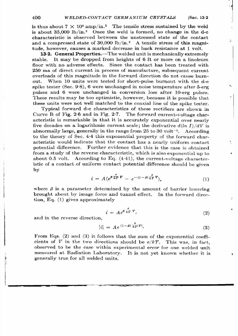
400
WELDED- ONTACT GERMANIUM CRYS TALS
~SEC.
132
‘1
is thus about 7 X 10⁶ amp/in.2
The tensile stress sustained by the weld
is about 35,000 lb/in. 2 Once the weld is formed, no change in the d-c
character ist ic is observed between the unst ressed sta te of the contact
and a compressed sta te of 30,000 lb/in. 2 A tensile stress of th is magni-
.;
tude, however , causes a marked decrease in back resistance at 1 volt .
302. Gen er sl P roper ties.-Th e welded u nit is m ech an ica lly ext remely
stable. It may be dropped from heights of 6 ft or more on a linoleum
floor with no adverse effects. Since the contact has been t rea ted with
250 ma of direct cur rent in process of manufacture, subsequent curren t
ov r loads of this magnitude in the forward direct ion do not cause burn-
out . When 10 units were tested for shor t-pulse burnout with the d-c
spike tester (Sec. 9.8), 6 were unchanged in noise tempera ture after 5-erg
t
pulses and 6 were unc anged in conversion loss after 10-erg pulses.
These result s may be too opt imist ic, however , because it is possible tha t ‘
these units were not well matched to the coaxial line of the spike tester .
Typica l forward d-c character ist ics of these rect ifiers are shown in
Curve B of Fig. 2.6 and in Fig. 2“7. The forward current -voltage char-
acter ist ic is remarkable in that it is accura tely exponent ia l over nearly
five decades on a logarithmic current sca le; the deriva t ive d(ln Z)/dV is
abnor ally large, ge era lly in the range from 25 t o 30 volt–l. According
to the theory of Sec. 4“4 thk exponentia l proper ty of the forward char-
acter ist ic would indica te that the contact has a near ly uniform contact
potent ia l difference. Fur ther evidence tha t th is is the case is obta ined
from a study of the reverse character ist ic, which is also exponentia l up to i
about 0.5 volt . According to Eq. (4”41), the current -voltage character -
ist ic of a contact of uniform contact potent ia l difference should be given
by
i = A(e~&~_ ~–(1–19):TV
),
(1)
where ~ is a parameter determined by the amount of bar r ier lowering
brought about by image force and tunnel effect . In the forward direc-
t ion , E q. (1) gives a ppr oximat ely
e
i = Ae~~T v,
(2) ‘
an d in t he r ever se direct ion ,
lil =
Ae “-d) filvl.
(3)
From Eqs. (2) and (3) it follows that the sum of the exponent ia l coeffi-
cients of V in the two direct ions should be e/ k T . This was, in fact ,
observed to be the case within experimenta l er ror for one welded unit
mea su red at Ra dia tion Labor ator y.
It is not yet kno\ vn whether it is ,
gen era lly t ru e for all welded un its.

SEC,
133]
NEGATIVE I-F CONDUCTANCE
401
Th e sprea din g resista nce r ca n, as expla ined in Sec. 4.4, be fou nd from
t he forwa rd ch ar act er ist ic in t he r egion of depa rt ur e fr om t he expon en tia l
cu rve. The values of r thus obta ined usually fa ll in the range from 2 to
4 ohms, which is abnormally low for a con tact of small dimensions. The
dynamic resistance of the welded rect ifier s a t zero bias is abnormally
la rge, usually in the range from 2 to 10 megohms. At 1 volt in the
rever se direct ion the resistance is about 10,000 to 20,000 ohms and
decr ea ses r apidly a t h igh er in ver se volt ages.
Beca use t hei la rge dyn am ic r esist an ce n ar rows t he video ba ndwidth ,
th e welded units a re genera lly not suitable for use a t zero bias as video
detect or s. Their resist an ce fa lls in t he desir ed ra nge (abou t 10,000 ohm s)
at an appropr ia t e forward bias, bu t
their la rge noise ou tpu t in th is condi-
t ion milita tes against their use.
13.3. Nega t ive I-f Conduct a nce.—
The nega t ive i-f conductance dis-
played by the welded-con tact unit s
under su itable condit ions was first
observed by Waltzj 1 who measured
their admit tan e a t 30 Me/see with a
br idge. In th is work the crysta l was
excit ed with abou t 1 mw of power
from a microwave (3-cm) oscilla tor .
Waltz found tha t the i-f conduct -
ance becomes nega t ive, if the r -f
load admit ta nce is su itably a djusted,
I
F Ic. 13. 1 .—Cu rr en t-volt age ch ar ac-
t er ist ics of welded-con ta ct r ect ifiers as
a ffect ed by r -f power .
and reaches magnitudes as h igh as severa l thousand micromhos.
If a
tuned circu it is a t tached to the i-f terminals, the tuned circuit will
oscilla te a t its r esonant frequ ency if the sum of it s shunt conductance and
the crysta l i-f condu ctance is zero.
Oscilla t ions of th is type have been
observed over a wide range of frequencies extending up in to the micro-
wa ve r egion , bu t n ever exceedin g t he excit in g fr equ en cy.
The negat ive i-f conductance can be conven en t ly displayed on an
oscilloscope. Th e 60-cps cu rren t-volta ge ch ara cter ist ic is pr esen ted on
the oscilloscope screen with a circu it of th e type shown in Fig. 10.11.
With no r -f (microwave) power applied to the crysta l th e cu rve looks
somewha t like Curve A of F g. 13.1. If a normal (nonwelded) crysta l
is used, the applica t on of r -f power of abou t 1 mw changes the shape
of the curve in such a way that it resembles Curve B of Fig. 13.1; in th is
ca se t he fin it e cu rr en t a t zer o bias is of cou rse, r ect ified cu rr en t.
Welded
units under similar condit ions may also produce a cu rve of type 1?, bu t
usually the curve looks like Curve C; there is a range of voltage near zero
] 11. C. ‘Walt z, p riva t e c mmunica t ion .
i
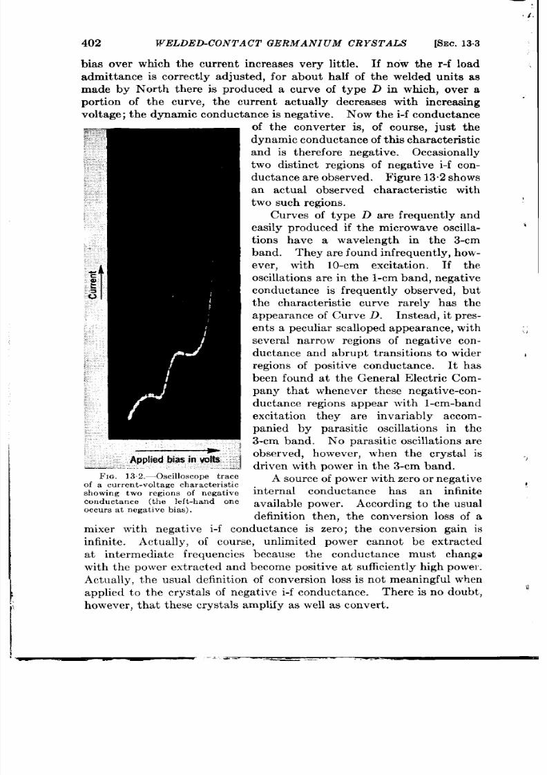
.$
402
WELDED-CON TACT GERMAN IUM CRYS TALS [SEC. 13.3
bias over which the cur ren t increases very lit t le. If now the r -f load .
admit tance is cor rect ly adjusted, for about ha lf of the welded units as
made by Nor th there is produced a curve of type D in which , over a
por t ion of the curve, the cu rren t actua lly decreases with increasing “
volt age; t he dyn am ic con du ct an ce is n ega tive.
Now t h e i-f condu ct a nce
showing two regions of negat ive
conductance (the left -hand one
occurs a t n ega tive bia s).
of the conver t er is, of cour se, ju st the
dynamic conduct ance of t h is cha ra ct er is tic
and is therefore nega t ive. Occasiona lly
two dist inct regions of nega t ive i-f con-
du ct an ce a re obser ved. F igu re 13.2 sh o s
an actua l observed charact er ist ic with
two su ch r egion s.
Curves of type D a re frequ ent ly and
ea sily pr odu ced if t he micr owa ve oscilla -
>
t ions have a wavelength in the 3-cm
band. They a re found infrequent ly, how-
ever , with 10-cm excit a t ion . If the
oscilla tion s a re in t he l-cm ba nd, n ega tive
conductance is frequent ly observed, but
the character ist ic curve ra rely has the
a ppea ra nce of Cu rve D. In st ea d, it pr es-
en ts a peculia r sca lloped appea rance, with :,,
severa l na r row regions of nega t ive con-
ductance and abrupt t ransit ions to wider ,
r egion s of posit ive con du ct an ce.
It has
been found at the Genera l Elect r ic Com-
pany tha t wh enever th ese n egat ive-con-
du ct an ce r egion s a ppea r wit h l-cm-ba nd
excita t ion they a re invariably accom-
panied by parasit ic oscilla t ions in the
3-cm band. No parasit ic oscilla t ions a re
observed, however , when the crysta l is
J
dr iven with power in the 3-cm band
A source of power with zero or negat ive ,
in terna l conductance has an infinite
available power . According to the usual
defin it ion then , the conver sion loss of a
mixer with negat ive i-f conductance is zero; the conver sion gain is
infin ite. Actua lly, of course,
unlimited power cannot be ext r act ed
a t in termedia te frequencies because the conductance must changa
wit h t he power ext ra ct ed and become posit ive a t suficien t l y high power .
Actua lly, the usual defin it ion of conversion loss is not meaningfu l when ,,
applied t o th e crysta ls of n egat ive i-f con duct an ce.
There is n o doubt , i
h owever , tha t t hese crysta ls amplify as well as con ver t.

SEC. 13.4]
LOS S AND NOISE MEASUREMENTS
40J
134. Loss and Noise Measurements.
Measu renwn ts of Con version
Loss. —Curious result s are obtained when convent ional appara tus is
employed to measure the
“ on ver sion loss” of t hese welded r ect ifier s.
Tests made with the 60-CPS amplitude-modula t ion method using a
3-cm oscilla tor have shown that considerably more 60-cps power can
be ext racted from the crysta l than is available in the modulat ion side-
bands of the oscilla tor . In one case the ra t io of the output power to
available input power was as high as 16 db.
A number of Nor th’s units were measured for conversion loss by the
Pound (impedance conversion loss) method (see Sec. 7.3). It was found
tha t at a proper bias poin t the indica ted conversion loss was unity. A
remarkable conse uence was that opening and closing the i-f terminals
had precisely the same effect on the amplitude of the reflect ed signal
w ve as opening and closing the r-f shut ter (Fig. 7.5). It appeared
that t here was a per fect los sles s connec-
and[e
t ion through the rect ifier between the r --- --------1
r -f a nd i-f sect ion s.
Noise F igu re.—Th e loss mea su re-
ments,
although in terest ing
significant,
a re not of themselves
sufficien t to determine the merit of
----- - J
Equivalent crystal circuit
t h es e cryst a ls a s fr equency conver t er s.
FIG.13.3.—Equiva 1ent in pu t cir cu it of
In addit ion, data on the noise output
t h e i-f amp lifier .
of the crysta ls are needed. Independen t measurements of conver .
sion loss and noise te pera ture,
however , a re possible only when
the i-f conductance of the mixer is posit ive. The significant quantity
in any case is the noise figure of the whole receiver including the mixer ,
and this quantity has a defin ite measurable value ir respect ive of the sign
of t he i-f condu ct an ce.
At Radiat ion Labora tory there was built an appara tus by Ber inger l
and ther s especia lly designed to measure the noise figure f a receiver
with a welded-contact conver ter and to assess the rela t ive influence on
noise figure of conversion loss (or gain) and of noise genera t ion . It has
already been descr ibed in Sees. 7“10 and 7.11 and illust ra ted in Figs.
7.15 and 7“16. Figure 133 shows an equivalent circuit of the input
t o t he i-f amplifier . Th e crysta l is r epr esen t d h er e, by Nor ton ’s t heor em,
as a conductance gd, which may have either sign, with two parallel
constant-c r rent genera tors (at i-f); one, i., represents the conver ted
signal, an d t he ot her ,
in ,
t he con ver ted an d gen er at ed n oise of t he cryst al.
No i-f susceptance is shown, as any such susceptance is tuned out b fore
eac measu r emen t .
1 E. R. Ber inger , C. P. Gadsden , and h f. C. }$7altz, “X-Band Noke Figu re Mess.
u rement s of Welded Cont ct Germanium Crystals, ” RL Group Repor t 53-
J u ly 16, 1945.

404 WELDED-CONTACT GERMANIUM CRYSTALS
[SEC. 134
The conductance g’ is made up of two parts; one, the shunt con-
ductance gl of the para llel tuned circu it , and the other , gz, an added
conductance which is switched in when measur ing the welded units,
since otherwise the tota l c nductance would genera lly be outside the
ca libr at ed r an ge of t he amplifier n oise figu re.
he method of measure-
men t is descr ibed in Sec. 7.10. (The conductance g, and g, cor respond
t o t he r esist an ces
R 1
and R2 of Fig. 7“15.) The quantit ies determined
by th e measu rements ar e t he over-a ll n ise figure, th e noise t empera tu re
t , and conversion loss
L
of the combinat ion of crysta l and load con-
ductance g’. Also the conductance g of the crysta l and the current s i.
and i. a r e determined. These data and a knowledge of the noise tem-
pera ture t , of the r -f signal source give a ll t he relevant information . For
example, if th e i-f con du cta nce g of th e crysta l is posit ive, t he con version
loss
L=
and noise t empera tu re t . of the crysta l it self a re given by
Lz=L~
96 + 9“
(4)
()
L=l+ 1+;
(5)
If the i-f conductance g~ of the crysta l is nega t ive, these result s do
not hold and, in fact , t he quantit ies
L=
and t . become nugatory. The
con version and noise genera ion of t he crysta l can st ill be descr ibed with
the aid of i, and i..
Thus, for an idea l amplifier genera t ing no noise,
the a t io of signal power to noise power at the amplifier ou tput terminals
i
is
t,
(6)
The noise figu re
F is
the noise tempera tu re t , of the signal source
when the ou tput signal-to-noise ra io is unity. Thus, wr it ing
F = FO
for an ideal amplifier , on e obtains
‘/
‘0“ ( ’ - %7 ) ”
This result , giving the lowest possible noise figure, holds, wha tever the
sign of gp, provided of course tha t g~ + g’ is posit ive.
Th e over -a ll n oise figu re ca n a lso be compu ted for a n on idea l amplifier
with noise figu re N > 1.
The result can be shown to be
(
=L
f–l+N~
)
9P + g’,. “

:.
I
i
SEC. 134]
LOSS AND NOISE MEASUREMENTS 405
Ber inger’ and his cowor kers first “made measurements for th e broad-
band case in which there is no discr iminat ion between signal and image
r-f tuning. The appara tus is tha t shown in Fig. 7.16 with the image
filter (magic T with cavity) removed. It was found tha t the over-a ll
noise figure changed lit t le as a funct ion of the posit ion and amount of
insert ion of the screw tuner and as a funct ion of the amount of local-
oscilla tor dr ive and the d-c crystal bias.
Although the outpu t noise
power changed by as much as 20 db in this adjustment , the noise figure
remained with in the range of 13 to 18 db. This constancy of noise figure
suggests that the ra t io of i-f noi e power to i-f signal power remains about
the same, tha t is, independent of the i-f conductance. Experimen s
confirmed this deduct ion . Table 13.1 shows measured values of i. as a
funct ion of crystal i-f conducta nce, with bias voltage and crysta l cur ren t
constant.
The conductance var ia t ion corresponds to different screw
insert ions.
TABLE
13.1 .—CRYSTAL I-F
SOISE CURRENT AS A FUNCTION OF I-FCONDUCTANCE FOR
DIFFERENT R-F TUNING
Q8
&
(arbitraryunits)
– 62 pmhos 1,7
- 30 2.0
8
2.0
+ 770 2.0
+1400
2.0
+3700 2.6
It is seen that in is pract ica lly constant over wide changes in g~. Since
the noise figure is nearly constant , i. must a lso change lit t le
Thus signal and noise power increase together as the conversion loss
decreases, and no improvement in noise figure result s. The suggest ion
has been made that the r -f signal source is ser iously mismatched when
the screw tuner is deeply inserted to give a negat ive i-f conductance.
If it were possible to decrease the i-f conductance by some other means
so tha t the signal impedance would still be at one’s disposa l, the noise
figure could perhaps be improved.
Beringer et al.z found tha t the i-f
conductance can be made very low, even negat ive, by reflect ng only the
image sideband. In th is work the ar rangement of Fig. 7.16 was
employed. A band-reject filter reflect ed the image frequency, with
reflect ed phase made adjustable by means of the “ line st retcher . ”
It was found that no improvement resulted from the reflected image
frequency and tha t the lowest noise figure was obtained ith both side-
bands matched. Table 13.2 summarizes these measurements. It
should be noted tha t the crysta l conversion loss is negat ive (expressed
1L ot. Cit.
2 L ot. tin t.

-T
406 WELDED-CONTACT GERMANIUM CRYS TALS
[SEC. 13.5
TABLE 13.2.—CONVEESIONAND NOISE PARAMETERS AS A FUNCTIONOF INDEPENDENT
TUNING OF THE R-F S IDEBANDS
Crys ta l i-f conductance
w produced by
Slgnal-
frequency
reflection
Low
High
Intermediate
(Matched
signal)
(Matched
signal)
Low
(Matched
signal)
Image-
frequency
reflection
low
low
low
low
high
high
(matched
signal)
9 p ,
mho,
58
1080
880
650
4000
3200
1900
t
9.9
3.9
4.2
4.7
1.5
1.7
2.1
i“, in
arbi-
t ra ry
units
2,0
2.
2.2
2.1
2.4
2.3
2.0
L, db
5.1
5,9
7.0
4.8
7.7
10.3
7.1
>., db
t=
–3.9
79.0
+4.5
4.6
+5.4
5,7
+2.7
7.0
+7.3
1.5!
+9.8
1,8
+6.3
2.3
‘o, db
14.6
11.5
12.9
11,1
8.7
12.3
9.1
F, for
3-db
ampli-
ier , d b
14.7
12.4
13.6
11.7
11.7
14.3
10.9
in db) in the case of i- conductance minimized by both signal- and
ima ge-frequen cy reflect ion s (fir st r ow of t he ta ble). F or an ot her crysta l
Ber inger was able to produce nega t ive i-f conductance by reflect ing the
ima ge fr equ en cy wit h t he sign al fr equ en cy m at ch ed.
The lowest noise figure obta ined (if an amplifier with a 3-db noise
figure is assumed) was 10.9 db. Although this figu re is well with in the
limit for 1N23B rect ifiers (the best 3-cm-band crysta ls) it is not spec-
tacular . In fact , the noise figures of many 1N23B crysta ls, with the
same amplifier , a re from 8 to 10 db.
La ter measurements by Nor th l substan t ia ted Ber inger ’s finding
tha t the best per formance occurs with a matched signal, cor responding
to high i-f conductance. Nor th was able, however , by cor rect bias
adjustmen ts and at rela t ively low loca l-oscilla tor dr ive, to obta in for
some crysta ls over-a ll noise figures again with a 3-db amplifier ) as low
as 6 or 7 db. These values were obta ined for match d signal and image
fr equ en cies a t r ela t ively h igh i-f conduct a nce.
It must be sa id th at n ot all possibi it ies for using t he welded-con ta ct
u nit s a s con ver ter s, u nder t he con dit ion of low or n e a tive i-f con du ct an ce
have yet be n exhausted. For example, it is possible (a lthough no;
likely) tha t a t a higher in termedia te frequency the noise ou tpu t may be
cons iderably reduced.
13.6. Th eor y of Nega tive I-f Con du ct an ce a nd Con ver sion Amplifica -
t ion .-The two anomalies of Nor th ’s crysta ls, conversion gain and nega-
I H . Q. Nor t h , et (d .,
“welded GermaniumCrysta ls ,” GE Final Repor t , Contract
0EMsr-262—Ordn.No, DIC 178554,Sept.20, 1945,
.
.

SEC.
13.5]
THEORY OF NEGATIVE I-F CONDUCTANCE 407
t ive i-f conductance, a re closely associa ted, if not concomitant . It is
clea r tha t a mix r with nega t ive i-f conductance will amplify, since
in the linea r approximat ion the ava ilable power from it s i-f t erminals is
unlimited. The conversion loss of such a mixer is exact ly zero. A
con version loss of unity, however , implies n o a ttenuat ion bet ween signal
and i-f t erminals, and a conversion loss in the range from zero to unity
implies amplifica t ion . Thus it is not necessa ry for a mixer t o have
nega t ive i-f conductance in order for it t o amplify. For example, the
data given in the first row of Table 13.2 should be not ed. The crysta l
refer red t o has a posit ive i-f conduct ante but a lso has 3 .9-db conversion
gain.
It can be shown by the methods of Chap. 5 that , under the condit ion
of weak reciprocity and provided the reciprocit y factor g.P/g~. is not
less t ha n unit y, no possibilityy of conver sion amplifica t ion exist s unless
t he i-f conductance becomes negat ive a t some r-f load admit t ance. The
proof is somewhat tedious and will be omit t ed. By methods similar
t o those of Sec. 5.10 it can be shown that values of r -f load admit t ance
exist for which the i-f conductance is nega t ive if, and only if,
712 > , (9)
where q~ is defined in terms of the elements of t he mixer mat r ix by
Eq. (5.73),
2g.@g~=
q2 =
9@6(9.. + 9.7)”
(lo)
Weak reciprocit y is assumed in proving Eq. (10). Measurement ’
of the mixer mat r ices for a number of welded unit s showed that weak
reciprocity held for a ll units t ested but tha t full r eciprocity fa iled for all.
The data on four of the units a re given in Table 13.3. The first r ow gives
TAZLE 133.-ADMITTANCE MATRIX ELEMENTS OF WELDED-CONTACT RECTIF IERS
Crysta l no. * D404
D401
D405
D574
en, volts
0.15 0 20
0.17
0.23
iO , ma
0.57
0.67
0.%3
0.52
P, mw 1.67
1,00
0.65
0.65
9J9Q
13,3
14,2
8.42 10,94
9.0/ GO
0.201
0.376
0.192
0,170
9aa / duo
0.116
0.206
0,145
0.110
9a7/90
6.68
7.20
2.42
2,44
98P
0.0021
0.0052 0.002
9@19P .
1.73
1.83
1,32
1.55
7?
1.11 0.99
0,99 1,07
q
In the fir .+ column g. is the character is t icconductance of the r- f t r snsmimion line or wa veg. id e.
Afl conductance, go, o.mx, etc. are gtven in mhos.
I
By L, Apk er , Gen er al E lect ric Compa ny, pr iva te communica tion .

408
WELDED-CONTACT GERMANIUM CRYSTALS
the d-c bias voltage (posit ive); the second, the crysta l cur ren t ; the
third, the available r -f power from the loca l oscilla tor ; the four th to eighth ,
the elements of the mixer mat r ix [see Eq. (5.13)]; the nin th , the reci-
pro it yy fa ctor g.~/gPa; and the tenth , th e quantity q, of Eq . (9) and (10).
Evident ly unit s D404 and D574 can exh ibit nega t ive i-f conductance,
but units D401 and D405 cannot (a t the par t icu lar bias and loca l-
oscilla tor level s ta t ed ).
F rom the theory of Sec. 5.7 it can be seen tha t the conversion loss,
with equal terminat ions a t the two r -f sidebands, can be less than uni y
on ly if E q. (9) h olds. Th us con ver sion amplifica tion is closely a ssocia ted
with nega t ive i-f conductance and the theory of one is essent ia lly the
theory of the other .
It will now be shownl tha t nega t ive i-f conductance can result if the
rect ifier is r epr esen ted as a nonlinear resista nce in shunt with a volta ge-
var iable capacitance, provided tha t the resistance (e.g., spreading
r esist an ce) in ser ies wit h t his combin at ion is su fficien tly small.
Th e linear rela tion s among th e cu rren ts and voltages a t signal, image,
and in termed a te frequencies have been der ived for a rect ifier of th is
type in Sec. 5.11 and are given by Eqs. (5197). In order to simplify
the analysis it is now assumed tha t a t ime zero exist s making the ba rr ier
voltage a t loca l-oscilla tor frequency an even funct ion of the t ime. In
a ccordan ce with th e discussion ollowing Eqs. (5.197), this assumpt ion
simplifies t he equ at ion s t o t he followin g form:
ia =
(gO + j~CJ e. + (g, + jWCJ eP + (92 + &C2)e*,
i~ =
g~ea
+ goefl + le~,
1
( 1 1 )
‘ i : =
( 9 2 – @C2)a + (9, – juC1)ed + (gO – .jd30)e~.
The above assumpt ion about the form of the loca l-oscilla tor wave is
exact ly t rue if harmonic voltages a re zero or a re co rect ly phased with
respect to the fundamenta l. In actua l fact the assumption is only
approximately t rue, but it is not believed tha t the qualita t ive con-
clusions reached will be affected by fa ilure of the assumption .
In Eq.
(11) ia , iB, and i, a re the terminal cu r rents a t signal, in termedia te and
im age fr equ en cies, r espect ively; a nd ea ,
e~, a nd e? a re t he cor respon din g
voltages. The quant it ies gn and C. a re, respect ively, the Four ier coeffi-
cien ts of the dynamic conductance and capacitance of the barr ier [see
Eqs. (5192) and (5193)].
Let us suppose, as an example, tha t the signal and image voltages are
terminated by the same load admit tance ya = ga + jba , hence,
iu = —ye.,
(12)
iY = — ymey.
(13)
1SW H. C. Tor r cy, RI, G roup Repor t 53, h lay 22, 1945.

SEC 1 3 5 ]
It can be
THEORY OF NEGATIVE I-F CONDUCTANCE
409
shown tha t , if the i-f conductance cannot become nega t ive
under th is symmetr ica l sideband condit ion , it cannot be nega ive for
a ny possible r -f loa d a dm it ta nce.
When i=, i,, ea , and e, a re elimina ted from Eqs. (11), (12), and (13)
and the equat ions a re solved for the i-f admit tance of the mixer , viz.,
~B=$
efl
(14)
= 96 + jbd,
we obtain b~ = O,
and
,,=go[’a+@(@%)12 +[’’’W9121G2,2, (,5,
(ba + COCO)2+ ga + go)’ – gi – u2Ci
where
‘ Z = ” z r %- c , ) + g ’ ( ’ - s )( g o - g , )g o n g , - %)
(16)
The task is t o discover under wha t cond t ions, if any, the i-f con -
du ct an ce gfl ca n becom e n ega tive.
The case of a constan t capacit ance
( , = C, = O) is examined first .
In th is inst ance Eq. (15) reduces to
( b a + o c o ) ’ + [ g ~ + ’ o oN+ - 9 ’
(
(90 92) 9.+92–:
go =
)
(b. + uC,)’ + (g. + go)’ – gi
~ (17)
It is clea r from an examinat ion of Eq. (17) tha t both the de omina tor
and numera tor of the fract ion on the r igh t a re a lways grea ter than or
equa l to zero for any Y. with posit ive rea l pa r t , provided that
gl s go,
(18a)
g2
s
go,
(18b)
29: <
- z =
go + gz.
(18c)
It will now be proved that th ese condit ions [Eqs. (18)] a re a lways
sa tisfied u nder t he a ssumpt ion of a symmet rica l ba rr ier volt age, pr ovided
tha t the d-c cha racter ist ic (with no r-f voltage applied) has no poin t
of nega t ive dynamic con du ctance over the range of the loca l-oscilla tor
volt age excurs ion .

410
WELDED-CONTACT GERMAN I VM CRYSTALS
[SEC. 135
The quant it ies gm are the Four ier coe5 ien ts of j’(e) according to
E q. (5.193), wh er e
i = j(e) (19)
is the equat ion of the d-c character ist ic.
The Four ier development of
j’(e) with th e assumption of a symmetr ica l bar r ier voltage e becomes
f’(e) =90+ 2glcosd+2g2cos2d+ . . . +;
(20)
hence
/
+.
9.=; _r
j’(e) cos nu t d(d).
Let
F(e) =
j’(e)
!
_~ j’(e) o!(a.!)-
(21)
(22)
By hypothesis, j’(e), and so also
F(e),
is grea ter than or equal to zero;
F(e) ~ O.
Also from Eq, (22),
r+.
) F(e) d (d )= 1.
—.
(23)
(24)
Now from Eqs. (21), (22), and (24),
\
+.
/
+.
gl = go
F’(e) cos d o?(d) ~ go
F(e) d (d ) = g,,
(25)
—r
—.
and
!
+.
\
+.
gz = go
F(e) cos 20.! d(u t ) s gO F(e) d (d ) = go.
(26)
-*
—.
Thus t he fir st two in equ alit ies [Eqs. (18a ) a nd ( 18b) ] a r e demon st ra ted.
To prove the th ird, it shou d be noted tha t from Eq. (26)
/
+.
g2 = go
F(e) (2 COS’d – 1) d(d),
(27)
—.
or
[
+.
go + g2 = 2go
F(e) cos2 d d(d),
(28)
and tha t , from Eq. (25),
.29:
— = 2go
go
Now, it is clear tha t
J –T
\
+.
1
F(e) cos d d(d) .
(29)
—.
P+ - L
r
(e) cos (d ) cl(d ) d (d ) >0,

SEC. 1 3 . 5 ]
THEORY OF NEGATIV I-F CONDUCTANCE
411
since the in tegrand is a lways gr ea t er than or equal t o zer o.
Th is reduces,
on expansion, to
U
+ *
1/
2
+.
F (e) Cos d d(d) s
F(e) cos’ d d(d).
(30)
—.
—.
From Eqs. (28), (29), and (30) we obta in
29; <
-ii=
go + gz~
(31)
which is t he t hir d inequality [Eq. (18c)].
It has thus been proved that the i-f onductance is never ega t iv
under t h e following condit ion s:
1. Con st an t ba rr ier ca pa cit an ce.
2. Local-oscilla tor volt age at the bar r ier is an even t ime funct ion
abou t some t ime zero.
3. The d-c character ist ic (with no r -f power applied) does not have a
n ega t ive slope wit h in t h e loca l-oscilla t or excu r sion .
4. The r -f load admit tance h s a posit ive rea l par t .
Condit ions 3 and 4 apply to all measurements in which nega t ive i-f
conductance is observed. Thus nega t ive i-f conductance is caused by
fa ilure of Condit ion 1 or 2, or both . It is con jectu r ed, but not proved,
th at fa ilure of Condit ion 2 alon e will n ot lea d t o n egat ive i-f conduct an ce.
Some exper imen ta l evidence in favor of th is con jectu re has been found
by Hahni a t Genera l Elect r ic Company.
It will now be proved that fa ilure of Condit ion 1 alone leads, under
cer ta in condit ions, t o n ega tive i-f con du ct an ce.
To do this we must
retu rn to the genera l expression Eq. (15) for g~. Let us make N the
numerator of the fract ion on the r ight -hand side of Eq. (15) and D it s
denominator.
Then gp is n egat ive, if eit her
N>O, D<O,
(32)
or
N<O,
D>O.
Now the equat ion , N = O, is the equa t ion of a circle in the (ga ,ba)-plane
with the cen t er a t b= =
—u[Co –
(gl/go)Cd, and go = –go[l – (gi/g;)l.
This circle is shown as Circle A in Fig. 13.4. It s radius is G [Eq. (16)].
Since gl S go, the cen ter fa lls in the nega t ive-conductance half of the
I (ga ,ba)-plane. All poin t s for which N <0 lie with in th is circle. Because
of the pr esence of the term oz[(gl/gO)Cl — C~]2in Eq. (16) for the radius
I
I See H. Q. Nor th et al.,
‘(Welded Germa nium r yst als,” GE Repor t, Con tr act
OEMsr -262, Or der No. DIC 178554, Sept . 20, 1945.
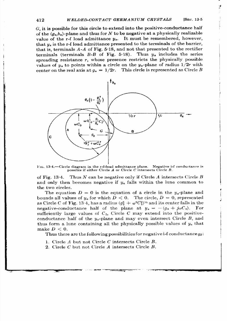
412
WELDED-CON TACT GERMAN IUM CRYS TALS
[SEC. 13.5
G’,
it is possible for th is cir cle t o ext en d in to t he posit ive-con du ct an ce h alf
of t he (g~,b~)-pla ne an d t hu s for N t o be n ega tive a t a ph ysica ~y r ea liza ble
va lue of the r -f load admit tance Y..
It must be remembered, however ,
tha t is, termina ls .4-A of Fig. 5.18, and not tha t presen ted to the rect ifier
termina ls (termina ls B-B of Fig. 5“18). Thus y. includes the ser ies
spreading resist ance r , whose presen ce rest r ict s th e physica lly pos ible
~~aluesof Y. to poin ts with in a circle on the ya-plane of radius l/2r with
cen ter on the rea l axis a t g. = l/2r .
Th is cir cle is r epr esen t ed a s Cir cle
B
%(1-
$
1~
9a -
I
]:lG.3,4.—Circle diagra m in th e r -f-load admitt ance pla ne. Negative i-f condu ct ance
possible if eit her Cir cle
A or
Cir cle C intersects Cir le B.
of Fig. 13.4. Thus N can be negat ive only if Circle A inte sects Circle B
and on ly then becomes nega t ive if y. fa lls within the lune common to
t he two cir cles.
Th e equ at ion
D = O is
the equat ion of a cir cle in the ya-plane and
bounds all va lues of Y. for which D <0. The circle, D O, represen ted
as Cir cle C of Fig. 13.4, has a radius (o3 + t i2C~)~fi nd it s cent er falls in th e
negat ive-conductance half of the plane a t Y. = —(go + jt iCo). For
sufficien t ly la rge values of Cj, Circle C may extend in to the posit ive-
conductance half of the y.-plane and may even in t er sect Circle B, and
thus form a lune conta in ing all t he physica lly possible va lues of ya tha t
I
4
i
make D < 0.
Thus t h er e a r e t h e following possibilit ies for n ega t ive i-f condu ct a nce gp:
1. Cir c e
A
but n ot Circle C in t ersects Circle
B.
2. Circ e C but not Circle A in t er sect s Circle B.
I
m
.. —-—
——
1
I
I
SEC.
13.5]
THEORY OF NEGATIVE I-F CONDUCTANCE
413
3.
Bot h Cir cle A and Circle C in ter sect Circle 1?, bu t t e two Iunes
th us formed a re n ot coin ciden t.
Since it can be shown the two lunes of Condit ion 3 can ever be
coin ciden t, it follows tha t if eit her Circle A or Circle C or both of them
in ter sect Circle B, physica lly possible va lues of ya exist for which th e i-f
conduct a nce is n ega t ive.
Condit ion 1 cor responds to the inequa lity of Eq. (33). In thk case
t he n ega tive-con du ct an ce r egion of Fig. 13”4 is bou nded by poin ts of zer o
conductance. This is the case commonly observed (Cu rve D of Fig.
13. 1) wh en th e loca l-oscilla tor wa velen gt h is in t he 3-cm band.
Condit ion 2 cor responds to the inequa lity of Eq. (32). In th is case
the nega t ive-conduct nce region of Fig. 13.1 is bounded by points of
infin ite conductance. Such a region has not as yet been observed.
Condit ion 3 includes both inequa lit ies [Eqs. (32) and (33)]. In th is
case the nega t ive-conductance region may be bounded by poin ts of
zero
conductance
on one
en d and in fin ite conductance
on
the other .
Th is ph en omen on h as been obser ved by Dick el for l-cm loca l oscilla tion s.
As a resu lt of th is analysis it can be concluded tha t th e qualita t ive
con dit ion s n ecessa ry for n ega tive i-f con du ct an ce are:
1. Barr ier capacitance must be var iable with ba rr ier voltage. The
var ia t ion must b st rong, so tha t Cl or C is la rge and Circle A
or C has a l rge radius.
2. The spreadi g resistance r must be small so tha t Circle B has a
la rge r adiu s.
3. The constant t erm C, in the Fou r ier expansion of the ba r r ier
ca pa cit an ce must not be la rge, since the sepa ra t ion of Circles A
and C from Circle B in cr ea ses wit h CO ( ee F ig. 13.4).
Now it is an exper im en ta l fa ct t ha t t he ba rr ier ca pa cit an ce of Nor th ’s
welded-con tact r ect ifie rs is a st ron g fu nct ion of ba rr ier volt age, at least
as st ron g a funct ion as for normal germanium rect ifier s.
It
is also an
exper imen ta l fact tha t th e spreading resist ance of the welded rect ifier
is abnormally sm ll for a con tac radius of 0.00 2 in . The small size of
t h e con t act is helpfu l in reducing the magn itude of CO. Thus it appears
th at t he welded-con ta ct r ect ifier s meet
th e qualita t ive condit ions for
nega t ive i-f conduct ance to a h igh er degr ee th an n orma l cr yst als.
Quan t ita t ive est ima tes of th va lues of r requ ired to give negative
i-f conductance have been made by Tor rey.z
Equat ion (1) was used
for j(e), and the values of g.
were
then compu ted as a funct ion of bias
volt age by u sin g va lu es of t he con st an ts A and ~ appr opr ia t e to t h e welded
rect ifier s. The barr ier capacit ance was assumed to vary wit h ba rr ier
1R. H. Dicke, private commun icat ion.
2H. C. ‘1’orr ey,un published.

414
WELDED-CONTACT GERMANIUM CRYS TALS
voltage according to Bethe’s Eq. (4”18) cor rect ed for values
[SEC.
1 3 5
of voltage
in the neighborhood of the contact potent ia l difference.
With Co = 0~2
ppj, Cl and Cz were computed. It was found that nega t ive i-f con -
duct ance of the type cor responding to the inequalit y of Eq. (32) could
occur if t he spreading resist ance r is less than 10 ohms, and of the type
cor r esponding to the inequa lity of Eq. (33) if r is less than 3 ohms. As ~
noted above, th e spreading resist ance of the welded unit s usually falls
in the range from
2 to 4 ohms and is therefore sufficien t ly low
t o
satisfy
t he t heor et ica l condit ion s for n ega tive i-f condu ct an ce.
Subsequent measurement s of dependence of contact capacitance on
volt age revea led tha t Bethe’s formu la , Eq. (4.18), does not hold well
for the welded unit s. These resu lt s were obta ined by compar ison of
microwave with audio-f r equenc y low-level rect ifica t ion efficiency;
the equiva len t circu it of Fig. 2.10 was assumed. This method was
descr ibed in Sec. 11.2. It was found that the bar r ier capacit ance was
near ly constan t with volt age for bias volt ages less than 0.2 volt s, bu t
t hereafter increased exponen t ia lly with voltage. It is expect ed that , if
t he ca lcu la ted va lues of c1 and CZ are cor rect ed in accordance with
these resu lt s, t he upper limit on r for nega t ive i-f conductance will
increase.
Hahn’ has made some in t erest ing exper imen ts wh ich th row ligh t on
the problem of nega t ive i-f conduct ance. He const ructed a low-fre-
quency ana logue of a crystal rect ifier by using a acuum-tube diode to
simulat t he nonlinear resistance of the bar r ier and a circu it employing a
react ance tube to simula te the var iable capacitance. The exper imenta l
circu it was designed to opera t e at an impedance level fifty t imes that of
the crysta and at a frequen y one twen ty-thousandth of the microwave
frequency (the la t ter about 10,000 Me/see). The circu it included
react ive elemen ts to simula te the whisker induct ance and the capacit ance
to ground of the glass bead that support s t he inner conductor of the
rectifier.
Hahn found that , when the var iable capacitance circu it was
disconnect ed, the “i-f conductance” of the equiva len t rect ifier cou ld
not be made nega t ive a lt hough the other element s of the circu it were
adjustable over wide ranges. When the capacit ance was caused to vary ,
ith vol age in order to simula te (with appropr ia t e sca ling) the observed
capacit ance var iat ion of the crysta ls, however , nega t ive i-f conductance
as defin it ely obt a ined. Hahn displayed the cur r en t -volt age charac-
ter ist ic of t he equiva len t rect ifier on an oscilloscope and was able to
duplicat e in every way the cor responding curves of an actua l welded ~
rect ifier (Fig. 13.1). He also found tha t the equiva lent ser ies spreading ~
resistance had to be sufficien t ly small befor e negat ive i-f conductance
appeared.
1H. Q. Nor th , t oe. cd
(
SIX,. 136]
AI’PLICA TION S 415
He discovered, too, that the value of the whisker induct nce was
fa ir ly cr it ica l for nega t ive i-f conduc ance. Nor th l la ter showed that
an altera t ion in the sh pe of th e whisker , and therefor e of its inductance,
affect ed the i-f conductance. For cer ta in whisker geometr ies, negat ive
i-f conductance cou ld not be obta in d a lthough all other factor s wer e
unchanged.
It is easonable to conclu de from th is wor k tha t the nonlinea r capaci-
t ance of th e ba rr ier is the con t rolling factor in the appea rance of nega t ive
i-f conductance, a lthough other elemen t s of the rect ifier a lso have some
influence.
1 .6. Applica t ions.-Although it has een found tha t the welded-
con ta ct r ect ifier of Nor th , in it s pr esen t form at lea st , ca nn ot t o adva nt age
replace the conven t iona rect ifier as a conver t er or video detector , it
st ill h as u tilit y in ot her a pplica tion s.
I has been found by D. Montgomery (see Sec. 5.16) tha t the welded
r ect ifier s a r e excellen t h a rmon ic gen er a tor s, bein g s up er ior t o conven t ion a l
types (e.g., t he 1N26)
in
the genera t ion of second and third ha rmonics
of 1.25-cm waves. Their super ior ity is especia lly marked as genera tor s
of the th ird ha rmonic. La ter work by N’or thz confirmed this resu t .
He also exper imen ted with welded con tacts of st ill smaller a reas and
found consid rable improvement in the genera t ion of 0.4-cm radia t ion
from a fundamenta l of 1.20-cm wavelength . Ber inger ’ has const ructed
silicon r ect ifiers th at a re per haps n ot grea tly in fer ior t o Nor t h’s crysta ls
in harmonic genera t ion , but a re mechanica lly and elect r ica lly nstable
by vir tue of their small con tact areas. The much grea ter stability of
the welded con ta ct gives it a marked advan tage. Some data in rega rd
to ha rmonic genera t ion by welded and conven t iona l rect ifiers a re given
in Sec. 5.16.
H en nelly4 h as con st ru ct ed germanium h igh -in ver se-volt age r ect ifier s
with welded con tacts. The techn ique used was similar in most respect s
t o N rth ’s, but with the difference t a t , following the lead of the Purdue
group, t in or n it rogen was used instead of an t imony as a doping agen t .
Hennelly found tha t h ighest in verse voltages and largest in verse resist -
ances occu r red with germanium prepa red by vacuum melts with no
added donors. The forward cur ren ts obta ined in th is case, however , were
low, on ly abou t 2 ma a t 1 volt . The most sa t isfactory rect ifier s were
made with vacuum-melted german ium with 0.2 a tomic per cen t of t in
added. In t is case, inver se resistances of 0.5 megohms at –40 volts
1H . Q. Nor th , 10C.cd.
‘ H. Q. Nor th , “A Compar ison of Silicon and Ger man ium Crystals aa H armonic
Gen er ator s of 4 mm an d 6 mm Waves, ” GE Repor t, J an . 15, 1946.
a Personal communicat ion.
4H. Q. Nor th et al.,
“Welded Germa nium Cr yst als,” GE F in al Repor t, Con tr act
0EMsr -262—Or dn . N o. DIC 178554, Sept . 20, 1945.

416
WELDED-CONTACT GERMANIUM CRYSTALS
[SEC.136
and .25 megohms at —50 volts were obta ined. The cur ren t a t 1 volt
forward \ vas about 16 ma (a t 25°C) in th is case. (“character ist ic cu rves
obta ined for pure germanium melted in dry n it roge exhibited proper -
t ies in termedia te bet \ \ -eent hose of va c~l(lm melt s \ vit h n o a dded impu rit y
and vacuum melts with 0.2 per c n t t in added. The stability ga ined
from welded con tacts is of grea t va lue for the h igh-voltage type, as for
ot her t ypes of r ect ifier s, a nd fu rt her wor k a lon g lin es in it ia ted by Hennelly
is desirable .
The accu ra te expon e t ia l law obeyed by th e forwa rd character ist ics
of an t imony-doped welded germanium re t ifiers is usefu l in circu it
applica t ions where a loga rithmic or exponen t ia l r esponse is desired.
Kallman has utilized th is principle n some d-c br idge circuits. In
par icu lar , he designed a double-br idge circuit for indica t ing the ra t io
of two dir ect volta ges o a logar ithmic sca le.
No use has yet been made of the amplifying proper t ies of the welded
r ect ifier s u sed a s conver t er s.
It is possible th at a ligh tweigh t r eceiver—
with no tubes, yet capable of detect ing audio modula t ion of a weak
microwave signal close t o n oise level—migh t be con st r ucted by keepin g
these crysta ls on the verge of oscilla t ion by a suitable feedb ck arrange-
ment Some work along these lines was sta r ted by Dicke, but incon-
clusive results had been obta ined when the war came to an end.
Nor th l has fou nd tha t welded rect ifiers, u sed as frequ en cy con ver ters
in the 3-cm band and biased outside of the nega t ive i-f conductance
character ist ic, will opera t e with low loss (3 to 4 db) a t reduced loca l-
oscilla tor dr ive. The noise ou tput is then comparable to tha t from a
convent ional rect ifier , and th e over-a ll receiver noise figures obta ined
a re excellen t (below 6 db).
1Pr iva t e communica t ion .
I

It will
Q“ form,
APPENDIX A
THE RECIPROCITY THEOREM OF DICKE1
now be proved that the mixer -admit t ance matr ix in
Eq. (5.6), is symmetr ica l about the ma n diagonal,
the “ low
provided
t h e following condit ion s a r e sa tisfied.
1. Thephase of theelect r ic field st r ength isuniform over the rect ifying
bar r ier or bar r iers of thern ixer .
2. A t ime zero can be, and is, chosen such that the elect r ic field
st r ength at the bar r ier is an even funct ion of t ime.
3. The curren t -density componen ts at the bar r ier d pend on ly on the
component s of the elect r ic field in tensity (and not , for example,
on their t ime der iva t ives). This r est r ict ion excludes the possibility
of a nonlinea r bar r ier capacitance.
The theorem will be proved by establish ing Rela t ions (5.49) and
(5.50).
The black box of Fig. 5.3 is sup osed enclosed in a region R bounded
by a sur face S inter sect ing the terminals which for conven ience a rc
assumed to be coaxia l. Since the volt age applied to the terminals is
per iodic in t im e, t he field qu an tit ies in R may be expr essed as a Four ier
series in the t ime
.
. = — m
.
H(t) =
z
Hne,wi
n=—.
.
J (t ) =
z
J~e,nwt
.=—.
From Maxwell’s equat ions, it follows that
(1)
curl H. — j.oEE. = J .,
curl E. + jupH. = O,
where t and ~, the permit t ivity and permeability, are funct ions of pos -
t ion , and E, H, and J are, r espect ively, t he elect ric field st r ength , t he
magnet ic field st rength , and the elect r ic cur ren t density. Let us con-
1R.
H. r .ic e, ‘(A Reciprocity Theorem and it s Applica t ion to the Measurement
of Gain of L!icrowave Crysta l Mixers, ” RL Repor t No. 16-18, Apr . 13, 1943.
417
418
CRYS T AL RECT IFIER S
sider var ia t ions of the field quant it ies obta ined by va rying the terminal
voltages.
Le t do denote a change resu lt ing from a var ia t ion of e, holding e,
const an t , and let d l denote a change resu lt ing from a var ia t ion of e I
holding e~ const an t . Thus,
d~, = O, d ,e, # O,
d le~ = O, d ,e, # O.
1
(2)
It is assumed for the who e region except the bar r ier tha
J = uE,
(3)
wh er e t he con du ct ivit y y u is a fu nct ion of posit ion .
At a r ect ifyin g ba rr ier
a t ensor rela t ion is a ssumed to exist between dJ and
d ll
and t he compo-
nen ts of the t ensor assumed to be funct ions of E. Thus,
~(k~ =
z
u(,4-,l)(E) d~t~).
(4)
1
Th e t en sor will be a ssumed symmet ric, h en ce
~(k,l) = ~(l,k),
(5)
The superscr ipt s signify car tesian component s. Making use of the
vector iden t it y,
dlv AX B= B.cur l A–A. cu r l B,
we obt a in
div (d& x d,E. – d,IL X dd3.) = doJ ~ od,E~ – d~n s d&m (6)
By Eq. (3), the expression on the r ight of Eq. (6) vanishes everywher e
except a t t he r ect ifyin g ba rr ier .
Let us now appl Eq. (6) to the bar r ier by forming the followi g sum
(t o bein g a con st a nt ):
ez]ti~”div
(d& x
dlE. –
dlI-L x ddl~)
n
.
z
e2’w’(d,J . . d,E. – d,J .. d,E.). (7)
n
Since
.
and
/
+:
d, . = ~
d, E(t)e-i”@’ dt,
.
—-
‘..
5
---- -c ——— ~ . . . . . . . .
APPENDIX A
419
we have
Usin g t he r ela tion
.
z
ei””=rf3(a),
n-—m
wh er e 6(u) is t he Dir ac &funct ion ,
~(a) = O
a#O
/
.
6(a) da = 1,
—m
we have
wh er e we have in tegr at ed over A holding tfixed.
Subst itut ing Eqs. (6) and (4) in to Eq. (7), we find
[d@t’’(2to – t)d&)(t) – d ,l?Y )(2to – t)doE(’)(t)l d t. (9)
Now a new time var iable t’ is introduced,
t=t ’+ to.
Thus the r ight -hand side of Eq. (9) becomes
2 / : : : ’ ;( k ’ ’ ’ ’ ~ - t ’ ’ ’
—
,ll(k)(to –
’)dd’z)(to + t’)] d t’.
According t o Condit ion 2 for the reciprocity theorem (see Sec. 5“5),
there exists a t ime zero with respect t o which dE is an even funct ion of

420
CR YS TAL R ECT IFIER S
t ime. Let tObe th is t ime zero. The preceding expression then vanishes
ident ica lly; from Condit ion 1, th is resu lt holds over th e whole barr ier .
Ther ight -hand side of Eq. (9) nowvanishes over theent ir eregion R.
In tegra t ing Eq. (9) over R and conver t ing to a surface in tegra l over S
by the divergence theorem we obta in
2“’””101s
d,Hn X d,En – d,Hn X doEn) . dS = O.
n
The field quantit ies vanish everywher over the surface except at the
terminals. At the d-c terminals the only term appear ing is tha t for
n = O. At the r -f terminals the only terms appear ing are for n = t 1.
The in tegra t ion over the terminals is st ra ight forwa rd nd, in
t ermin al volt ages a nd cu rr en ts,
2(d&dle0 – ci i,doe,) + Re [e2~W’O(dOi,dlel– dlildoel)l
From Eq. (2),
d ,eO = dOe, = O;
hence,
2d&dOe0 = Re (e2@”dOi ,d ,el).
t erms of the
= o.
(lo)
The rela t ions between the var ia t ions of the terminal cur rents and
voltages are given by Eq. (5.15). Substituting Eq. (5.24) in to Eq.
(5.15), we fin d
d io = gb eO + ~yP&el + ~y~m de~
d il = 2y.&eO + y..de1 + y.ydc~.
}
(11)
Subst itu t ing Eq. (11) in to Eq. (10) we obtain
Re [(v8. – ~ape’~”’”)d,e,] = O.
Since the phase of d lel is a rbit r ar y, we h ave
yfla = ya~e21@t”, (12)
which is t he fir st of the reciprocity rela t ions, Eq. 5.49).
If, in st ea d of defin in g d , and d , by Eq. (2), we define them instead by
d ,io = doi, = O,
d ,i, # O, d ,io # O,
and foUow a similar pr ocedu re, we obta in
y& = ya7f# i~10 ,
wh ich is t he secon d of t he r ecipr ocit yy r ela tion s, Eq. (5.50).
(13)
..
SKIN EFFECT AT A
APPENDIX B
METAL-SEMICONDUCTOR CONTACT’
The skin depth c1in a conductor of dimensions large compared with 6
is given by
(1)
where j is the frequency and p and u are, respect ively, the permeability
a nd con du ct ivit y of t he con du ct in g ma ter ia l.
For tungsten we may take p = pOand u = 1,8 X 10⁵ mho cm–l. In
this case we have, for
j = 3
x 10’ Cps,
6 = 2.2 X 10⁻⁴ cm;
j = 1 x 10’” Cps, 6 = 1.2 X 10⁻⁴ cm;
j ==2.4 X 10’0 CPS, 6 = 0.65 X 10⁻⁴ cm.
In the case of silicon and germanium as used in rect ifiers, t he con-
duct ivity is less than tha t of tungsten by a factor of 10-3 or 10-4 and the
skin depth is thus grea ter by a factor of 30 to 100. Now the radius of
the rect ifying contact var ies from 10–3 cm to 2 X 10⁻⁴ cm. There is
thus in genera l an appreciable skin affect in the ca t wh isker a d prac-
t ica lly non e in t h e sem icondu ct or .
The above est imations do not apply,
however , to the immediate neighborhood of the semiconductor-meta l
contact . To find the spat ia l dist r ibut ion of current at the contact we
must solve a boundary-va lue problem, taking in to account the dis-
cont inuity in conduct ivity. In this way it can be determined whether
the redist r ibut ion of curren t -flow lines from a decided skin effect in the
wh isker t o a n egligible effect in t he semicon du ct or (1) t akes pla ce mostly
in the metal; (2) takes place most ly in th e semicon du ctor ; or (3) is divided
about equally bet ween them.
The solu t ion of th is problem is presented here. It will appear tha t
Alt ern at ive (1) is t he cor rect on e; t he skin effect at t he con ta ct is t her efor e
in gen er al ver y small.
As a simple model there will be considered two semi-infin ite r ight -
circu lar cylinders, one of metal M, the other of semiconductor S having
the same diameter and connected coaxia lly with a nonrect ifying butt
join t as shown in Fig. (B 1). Although th is model is much simplified
it will be shown that the conclusions drawn from it apply to the more
genera l case.
1H. C. Torrey, “Colloquium on Crystal Rect ifiers ,“Vacuum Tube Development
Commit tee Offices,New York, N. Y., June 17, 1944.
421
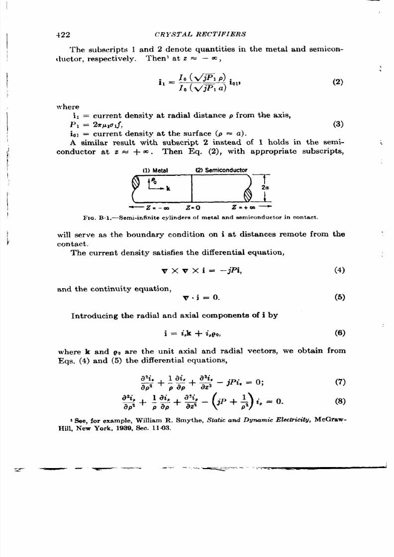
I
422
CRYS TAL RECTIFIERS
The subscr ipt s 1 and 2 denote quant it ies in the meta l and semicon-
1
doctor , respect ively. Theni a t z = — m,
(2)
where
i I = cur ren t density a t radi l distance from t he axis,
PI = Zrpxrlj,
(3)
iol = cur ren t density a t the su r face (p = a).
A similar resu lt with subscr ipt 2 instead of 1 holds in the semi- .
.
f
conductor a t z = + m. Then Eq. (2), with appropr ia te subscripts,
t
[
I
[1)Metal
G!)semiconductor
I
I!EZ133
I
—Z. -m Z=o
z=+m —
1
FIQ. B.1 .—Semi-in fin it e cylinders of meta l and semiconductor in contact
~
will serve as the boundary condit ion on i a t distances remote from the
contact.
Th e cu rr en t den sit y sa tisfies t he differ en tia l equ at ion ,
VXv Xi=
– jPi, (4)
a ncl t he con tin uit y equ at ion ,
V.i=O.
(5)
In t roducing the radial and axial component s of i by
i = Lk + ippo,
(6)
where k and 90 a re the unit axia l and radial vector s, we obta in from
Eqs. (4) a nd (5) t he differ en tia l equ at ion s,
(7)
(8)
I See , for example,William R. Smyt h e, St a tic a nd Dynam ic E ’lect r ieit y, McGraw-
H ill, N ew Yor k, 1939, Sec. 1103.
___ — —
— ---- -- -.

APPENDIX B 423
These equa t ions a re to be solved subject to the boundary condit ions,
(a)
for i.;
atz=+~,
~z=lo(mp) . .
1,(@ a) ‘0’
(9)
(b)
atz=C,
(L) 1 = (i.),;
(lo)
atp=O,
i. is iin it e;
(11)
for i,;
a tz=+m, iQ = o;
(12)
a tp=O era ,
ip = o;
(13)
(14)
The last condit ion ensures the con t inuity of the tangent ia l componen t
of t he elect ric field vect or a cr oss t he con ta ct .
By standard methods we find a genera l solu t ion of Eq. (8) which
sa tisfies Con dit ion s (12) a nd (13)
In m et al:
iol =
2
B ,*J
n
In semiconductor :
( )
.p
v— ;
iP, +~’.z
—e
a
“2= LB’.J’t$)e-v’p’+%”=;
n
(15)
(16)
where zn(n = 1, 2, . . ) a re the root s of
J,(z) = o,
(17)
and J l(z) is the usual Bessel funct ion (its subscr ipt is not to be confused
wit h su bscr ipt s u sed t o dist in gu ish met al fr om sem icon du ct or ).
To sa t isfy Eq. (14) we must have
(18)
The corresponding solu t ions for i. a re now found from Eqs. (7) and
(5) :
‘lz=~(p)+~J j::$ BnlJ opl:)e+i~’%.; (19)
i,.=j,(,)-~~% .,.l, @.~~-~P+%z; (20
424
CRYS TAL RECT IFIER S
where
f(P) =
10 (mP) ~.
10 (@a) “
(21)
.
As they stand, Eqs. (19) and (20) obviously sat isfy Eq. (9). The
only remain ing boundary condit ion to be sa t isfied is Eq. (10). This
condit ion , with Eq. (18), determines Bln and Bz..
pu t t ing (i.), = (i.)z a t z = O in Eqs. (19) and (20),
we get
(22)
where
’ 2 3
The coefficients An a re now determined from Eq. (22) by use of the
well-kn own or th on orma l pr oper ties of t he Bessel fu nct ion s.
The fina l
r esult for B. is
where
i. W@ “aI, (v’F a)
a = (jPaz + z~)IO (WP . a)’
and
(25)
(26)
Expressions (24), (25), and (26) are now subst itu ted in (20). Put t ing
z = O and assuming UZ<< u 1 we obta in for the axia l component of cur ren t
density a t th e con ta ct ,
.
z
nP
J o ~
i. = j2(p) + iP2a2
~O(zn) <(z: +
j~laz) (z: + jP2a2J
(27)
n=l
where z is the mean axia l cu r r en t density,
In (27) the root z“ = O is excluded from the summat]on.
Now the cur ren t density is en t ir ely axia l a t
p = O
and
p = a.
To
est ima te the magnitude of the skin effect a t the con tact , two quant it ies
APPENDIX B
425
II
rom Eq. (27), will be computed, viz., = 2
a d the phase shift in
.(P-a)
iCfromp=Otop=a.
These two quantit ies give all the relevan t informat ion . The first
gives the magnitude of the hea t ing effect and the second bears on the
qu est ion of t he va lidity of on e of Dicke’s con dit ion s for r ecipr ocit y.
The magnitude of both effect s will turn out to be small. There can
then be used a
jortiori
arguments to show that the effects a re even
sm ller for t he ca se of an actual rect ifier including th e nonlin ear it of th e
con ta ct r esist an ce a nd t he differ en t geom et ry.
As an example we take,
a = 1.1 x IO–3 ~m
f=3xlo9 Cps
U2 = 50
mho/cm.
lVe then find
p,a ’ = 1.46 X 10–Z
P@’ = 53.1.
From Eq. (27),
i. = z(1 + 1.28 X 10⁻³ + j5.01 X 10–3)
(P = a),
i. = Z(I – 0.959 X 10⁻³ – j2.43 X 10–3)
(p = o).
The phase shift over the contact is then 7.4 X 10⁻³ radian , or 0.42°.
If Ali12 is the difference in the square of the abso ute va lue of the
axial cu rr en ts a t p = O and p = a, we have
Ali12
— = 2(1.28 + 0.96) X 10-3
Ii]’
= 4.5 x 10⁻³.
The heat ing effect is, therefore, less than one-half of on e per cen t .
It is in terest ing to note tha t , a lthough the ski effect is small a t the
con ta ct , it is st ill m uch la rger t her e t ha n in t he body of t he sem icon du ct or ,
wh ere th e clifferen tia l hea t ing is of th e or der 10–5 or O.01 per cent .
The effect a t the frequency 3 X 10⁹ cps has been computed for about
the largest con tact it is pract icable to use at tha t frequency. The maxi-
mum size of the con tact a t h igher frequencies will be less.
Th e conver -
sion loss is rough ly a funct ion of fCr (as we saw in Sec. 4.5), where C
is the ba rr ier capacitance and r the spreading resistance. NOW, C u a’
and r cc l/a , so the 10SSis a funct ion of fa . The skin effect , however ,
depends on fa2. If we assume that fa (or loss) is kept constant by
decreasing a as the frequency is increased, then ja’, and hence the skin
effect , will be less a t h igh er fr equ en cies.

426
CRYS TAL RECT IFIE RS
Fur thermore, the skin effect for the actua l geomet ry of a rect ifier ,
in wh ich the s miconductor is a semi-in fin ite cylinder of la rger dimen-
sions, will be less than for the geomet r y of the model assumed. Fina lly,
t he effect of the non linea r r esis ance can on ly decrease the skin effect ,
since the effect ive conduct ivity will be less than tha t of the bulk
semiconductor.
It follows fr om t his r ea son in g t ha t t he skin effect is en tir ely n egli ible
for a ll poin t -con tact r ect ifier s a t any microwave frequency and the
cu rren t flow a t the con tact may be t r ea t ed with the d-c approximat ion .

APPENDIX C
SPREADING RESISTANCE OF AN ELLIPTICAL CONTACT
The con tact su r face between meta l and semiconductor is approxi-
ma ted by an ellipse of semidiameters a , b (a >> b) and r ect an gu la r a xes
chosen so tha t the x-y plane conta ins the con tact su r face, the long
dimen sion of th e con ta ct bein g along t he z-axis. Ellipsoidal coordin at es
& ~, q a re now defined by
j(o) =
&e + ~+-. + ; = 1,
(1)
where 0 s ands for any one of t e t r iplet (~, f, q) and
The confocal ellipsoids, f = constan t , a re the equipoten t ia l su rfaces
of the problem, since for ~ = O, j(~) = 1 degenera tes in to the ellipt ica l
con tact . Laplace’s equa t ion for the potent ia l V becomes
[
1
; <(t +
~’)(t +
b’)ta: =
O.
Thus,
/ 4
“=.4
E
d(
o
(t+ a’)(t + b’);
(2)
where A is a n in tegr at ion con st an t.
Ac ording to Eq. (2), V = O at the whisker con tact , and if V = VO
(the applied poten t ia l) a t ~ = ~,
Thus Eq. (2) becomes
v“~sn-’(dg+
where
(3)
r
= 1–$,
and
K = sn-’ (l,k)
4 2 7
428
CRYSTAL RECTIFIERS
is the complete ellipt ic in tegra l of the first kind with modulus k. N ow
if r is the radia l distance from the cen ter of the contact , as r becomes
large, &
= T2and
v
( )
a
‘vol–lG -
The curren t is thus
where o is the conduct ivity; and the resistance is
R=~.
%sa
(4)
Th is r esu lt is gen er al.
So far , the condit ion tha t a>> b has not been used. In fact , if a = b,
then K = Ir /2 and R = l/4ua, the well-known result for a ircu lar
contact of radius a. If a>> b, k = 1, and K = in (4a/ b). Thus for
a lon g, thin con ta ct ,
ln4~
R=—b
2mra
(5)
:

APPENDIX D
CRYSTAL-RECTIFIER TYPES AND SPECIFICATIONS
The specifica t ions on elect r ica l per formance of the var ious crysta l
types as of September 1945 are listed in Tables D-l, D2, and D“3. The
mech an ica l t est s a re summar ized in Sec. 2“2.
A summary of the J AN specifica t ions for the mixer and video crysta l
types is given in Tables D“ 1 and D. respect ive y. The ten ta t ive specifi-
ca t ion s on th e Western Elect r ic h igh -in verse-volt age types wer e wr it ten
join t ly by the Bell Telephone Labora tor ies, Radia t ion Labora tory, and
the NDRC group at Purdue University and have not yet been incorpo-
E
r ‘(i: ;4,
*0,0.?0
0.820
+0.C05
0.052
*0015
o.76a
*0.C03 0. 87
min.
Silicoflcrystal
.19
d
a~e O. 90
max.
‘“’’’S’”<
,.= -
I fip 2+?’
0.294 &~
20,015 0.240
(,
0,210
ream,
LL ~
{, f
‘
0.005max. rad.
0.010 max. rad.~
r
0,010 min. .0,046 max. rad,
FIG. D] .—Mech an ica l design specifica tion s for t he cer am ic ca rt ridge
ra ted in the J AN specifica t ions.
The 1N34 rect ifier was in it ia ted by
Sylvania Elect r ic Pr odu cts, Inc. and will probably so n be available from
othe r manufactu rer s .
Test methods and equipment tha t meet the requiremen ts of the J AN
specifica tions for test in g mixer and video cr ysta ls a re descr ibed in deta il
in Ch aps. 9 a nd 11 r espect ively.
Equ ipmen t for t est in g t h e h igh -in ver se-
volta ge t ypes listed in Table D.3 was descr ibed in Chap. 12.
The mechan ica l design specifica t ions for the ceramic and coaxia l
car tr idges a re shown in Figs. D.1 and D.2, r espect ively.
Comm ents on the Speci$ca tion s.—Th e wa velen gt hs given in Column z
of Tables D”1 and D”2 designa te the approximate region for which the
var ious t pes a re adap ed. Rect ifiers passing the tests a t a par t icu lar
I Th e qu an tit ies listed in Column s 4—13 a re ta ken fr om t he JAN specifica tion s.
No at tempt has been made to include all of the deta ils of these specifica t ions. For
complet e d et a iled in forma tion t h e r eade r is r efer r ed t o t h e join t Army-NTavy Specifica -
in to JAN-1A for E lect ron Tu bes.
429

;
430
CRYS TAL RECTIFIERS
radio frequency will in genera l be as good in conversion loss a t lower
frequencies. The conver se may not , however , be t rue. The types
designed for h igher radio frequency usually a re adjusted for smaller
con ta ct a rea t o a ch ieve a sma ller ba rr ier sh un tin g ca pa cit an ce.
This a t :
t he same t ime makes for lower burnout .
The specifica t ions, moreove r ,
which call for specified r -f and i-f matching condit ions in the t est equip-
ment tend t o insure uniformity in r -f nd i-f r ect ifier impedances. These
conside a t ions make it advisable to us the var ious types only for the
fr equency band for which they were t est ed.
The var ious mixer types with in each band a re, with one except ion ,
in ter ch an gea ble as fa r as impeda nce-m at ch in g pr oper ties a re con cer ned.
.,
0.012 ra diusk
FIG.
D. Z,—Mechanical design specificat ions for the coaxial car t r idge. The cr imp in the
car tr idge may be omit ted if desir ed.
They differ on ly in sensit ivity and burnout . The one except ion is type
1X28, which differs from the 1N21 types in r -f and i-f impedance. The
dist r ibut ion in i-f impedance cen ter s around 250 ohms, compared with
400 ohms for the 1N21 types. The r -f tuning of the t est mixer is in each
ca se st andardized a t th e cen ter of th e r -f impeda nce sprea d of repr esent a-
t ive samples fr om t he va riou s ma nu fa ct ur er s.
Each unit is subjected to the burnout proof t est and a small specified
representa t ive fr act ion of the tota l product ion to the burnout design
test.
The types for which the burnout t est va lue is listed in ergs a re t ested
by subject ing the rect ifier to a single video pulse of shor t dura t ion com-
pared with the thermal relaxa t ion t ime of the rect ifier contact . The
value listed in the table is the amount of energy dissipa ted in the crysta l.
The types for which the burnou t t est va l e is listed in wat t s a re t est ed
by subject ing the crysta l to a number of video pu lses of l+sec duration ,
a time long compa d with the thermal relaxation time of the crystal.
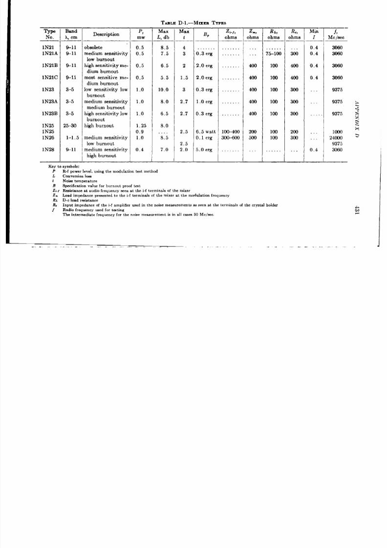
TABLE D.1 .—MmEB TYPES
;.:
1N21
1N21A
IN21B
1N21C
1N23
1N23A
1N23B
1N25
1N25
1N26
1N28
Band
A,cm
9-11
%11
9-11
9-11
3-5
>5
3-5
25–30
1-1.5
9-11
Description
obsolete
medium sensi t iv ity
l ow bu rnou t
h igh sens it i vi ty me -
d ium bur n ou t
m os t s en sit ive m e-
d ium bur n ou t
low sensi t iv ityy low
burnout
medium sensit ivityy
med ium bur n ou t
h igh sens it i vi ty l ow
burnout
h igh bu rnou t
mediurn sensi t iv ity
l ow bu rnou t
medium sensit ivityy
h igh bu rnou t
P,
mw
0.5
0.5
0.5
0.5
1.0
1.0
1.0
1,25
0,9
1.0
0.4
Ma x
L, db
8.5
7.5
6.5
5.5
10.0
8.0
6.5
8.0
“8:5
7.0
Max
t
4
3
2
1.5
3
2.7
2.7
2.5
2.5
2.0
0.3 er g
2.0 er g
2.Oerg
0.3 er g
1,0 er g
0.3 er g
6.5 wa tt
0.1 er g
5.0 er g
z;.,,
ohms
. . . .
. . . . .
IOG400
300-600
z
-,
ohms
400
4 0 0
400
400
400
200
500
RL,
ohms
. . . . . .
75-1oo
100
100
100
1(K)
100
100
100
Key to symbols:
P
R-f p ow er l ev el , us ingthe modulat ion test method
L
Convemion Iw
t
Noise temperature
B
Swci fimt ion value for bu rnou t mmf te st
Z;.! Resistance at au dio freau en cv seen at the -f t er mina ln of the m ixer
z.
Load impedr mce P rem n;ed t ; the i-f t er min als of the mixer at the modula tion frequen cy
RL D-c l oa d r es is ta nce
R.
Input im~dance of the i-f am plifier m ed i“ the n oise mea su rem en ts m seen at the t er min als of t he cr yst al holder
/
Ra dio fr equ en cy m ed for t en tin g
Th e in ter media te fr equ en cy or t he r mia e m ea wu em e,,t is in a ll ca ses 30 Me/see.
R.,
ohms
&
400
400
300
300
300
200
300
. . .
., ..
—.
Min
I
0.4
0.4
0.4
0.4
.,.
.,,
,,.
0.4
.,. ,.
j!
Mc /see
3060
3 0 6 0
3060
3033
9375
9375 L
k
5
9375
.?
<
c
1000
z
24000 e
9375
3ofXl
ti
.,, ,., ,,
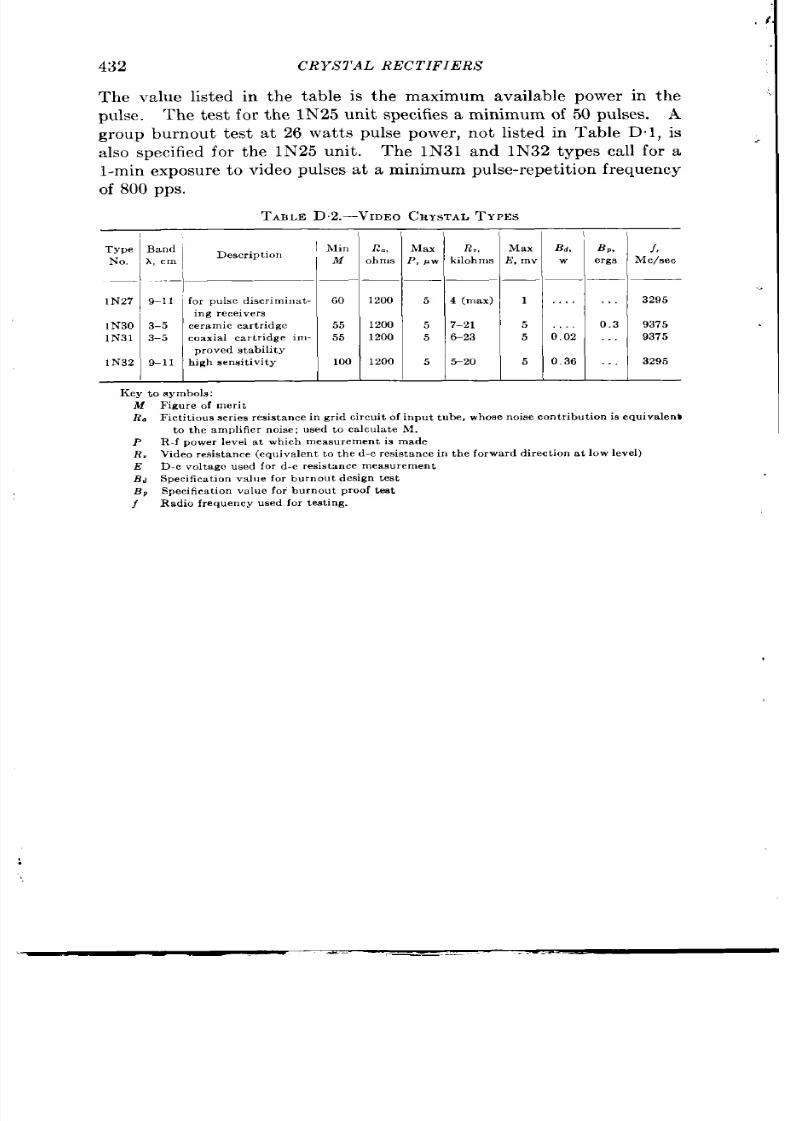
432
CRYS7’AL RECTIFIERS
The value listed in the table is the maximum available
pulse. The test for the 1N25 unit specifies a minimum of
group burnout test a t 26 wat t s pulse power , not listed in
power in the
50 pulses. A
Table D. 1, is
~lso specified for the 1N25 unit .
The IN31 and 1N32 types ca ll for a
l-rein exposu re t o video pulses a t a minimum pulse-r epet it ion frequ en cy
of 800
PPS.
TABLE D2.-VI~EO CRYSTAL TYPES
Type
No.
1N27
1N30
1N31
1N32
Band
Deacriptim,
A, cm
9–11 for p ulse discr im in at -
in g r ece, ver s
3–5
cer amic ca rt r id g.
3–5 coaxial car t r idge ml-
pm ved st a ih ty
9–11 h igh sensit ivity
h l,n E.,
M
ohms
1-
60
1200
55
1204
55
1200
100
1200
Max
P , /’w
5
5
5
R.,
k iloh m .s
(m ax)
7–21
&23
>20
Max
E, mv
1
5
5
5
B,,
w
,,.
0.02
0.36
.
B,,
ergs
0.3
,,.
//
Me/me
3295
9375
9375
3295
Kev to mmhols:
M
R.
P
R.
E
Bd
B,
f
Fiu”re of mer it
F,ct it ioua ser lea r esist an ce in m id circuit of input t ube, whose n oise con tr ibut ion is equ ivalen t
to the amphfi.r no,se; used to calcula te M.
R-f power level a t which measur emen t is made
Video resist ance (equ iva len t to the d-c resist ance in the forward dir ect irm a t low level)
D-c volt am used for d-c resistance measuremen t
Specifica tmn va ue for burnout design test
Specificat ion value for burnout proof t eat
Radio frequen cy u sed for test ing.
{.
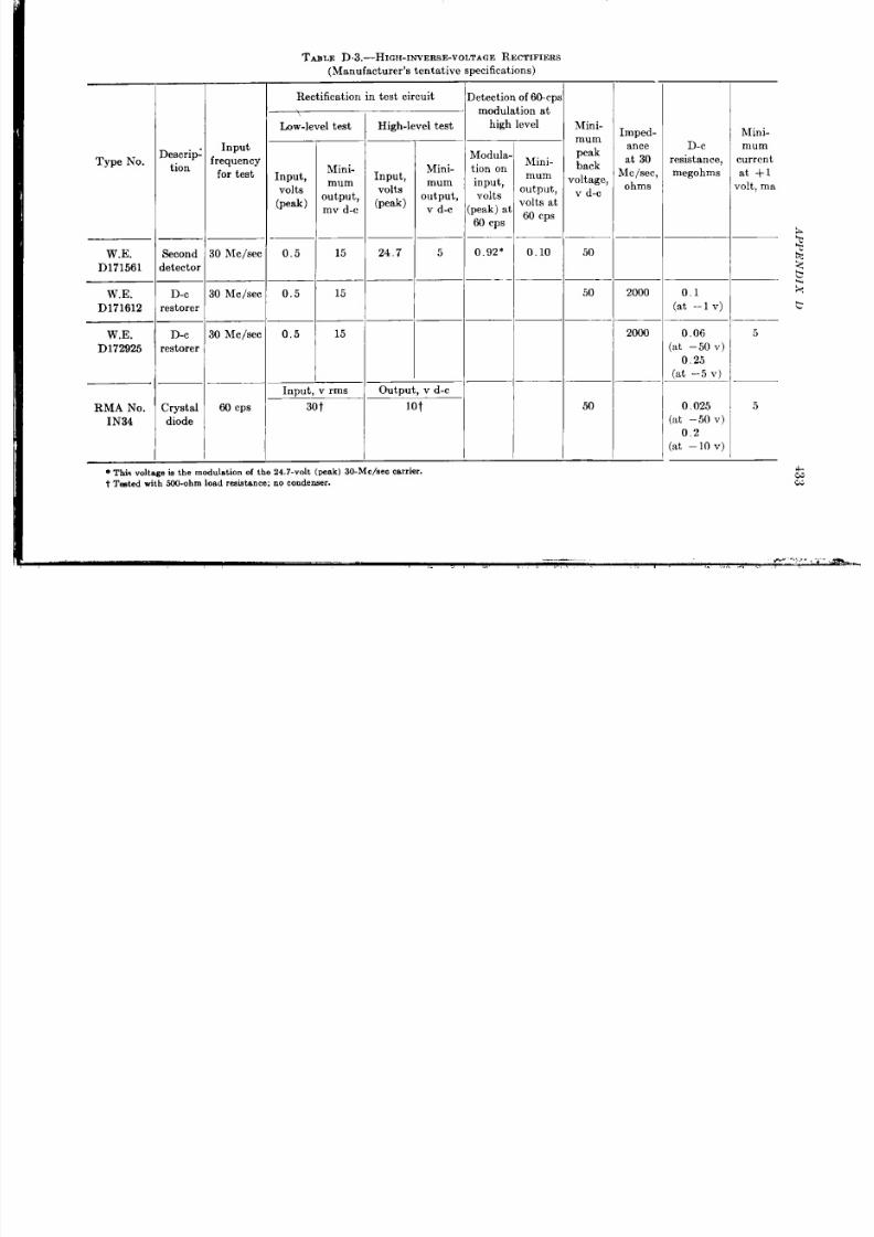
TABLE D.3.—H IGH -INVE RSE-VOLTA E RECTIF IERS
(Manufac turer ’s ten ta t ive speci fica t ions)
)et ect ion of 6 L
m odu la tion a l
h igh le vel
Rect ifi ca t ion in t e st ci rcu it
\
Low-level tes t
High- leve l tes t
Mini-
mum
Imped-
ance
at 30
bfc/sec
ohms
Mini-
mum
current
a t +1
Jo lt . ma
D-c
resistance,
megohms
Input
frequency
for t es t
Descrip~
tion
Second
detector
D-c
restorer
D-c
restorer
Crystal
diode
Moduh
t ion on
input,
volts
p ea k) z
6 0 cp s
0.92”
Typ e N o.
Mini
mun
OutpL
volts
60 CI
0.1(
~ack
voltag
v d-c
Mini-
mu m
outpu t ,
V d -c
Mini-
mum
output,
m v d -c
15
15
15
Input ,
volts
(peak)
0.5
0.5
Input,
volts
(peak)
)0 Me/see
24.7
5
50
w.E.
D171561
50 2000
2000
0.1
(a t – 1 v)
W.E.
D171612
)0 Me/see
5
W.E.
D172925
10Me/see 0,5
0.06
(a t –50 v)
0.25
(a t –5 v)
Outpu
1
V d-c
t
In pu t, v r ms
RMA No.
IN34
60 cp s
30 t
50 0.025
(a t –50V)
0.2
(a t – 1OV)
5
*Th is volt age in t he modu la t ion o f the 24.7-vol t (peak ) 30 -Mc/nec ca r r ie r .
tTmted with 300-ohm load re si st ance ;no condense r.
Index
A
Accep tance t est ing, 128
Acceptors , 47
Addit ion a gen ts, 67, 306-308, 364
(S ee a ko pa rt icu la r a ddit ion a gen t )
Admit t an ce ma t rix, 114-118
in terms of measurable parameters,
119-124
Adm it ta nce m at rix elem en ts of welded-
con tact r ect ifie rs , 407
Alumin um , a s a ddit ion a gen t, 67
Amer ica n Lava Cor por a tion , 3 3
Am plitude-m odula tio m eth od of loss
measu rement , 21$218
An geUo, S. J ., 307, 315, 321
An tim on y, a s a ddit ion a gen t, 67
Apk er , L., 126, 166, 174, 175, 407
Ar t ificia l ba r r ie r, 75
.4t t enuat or , m icr omet er , 275
vane-t ype, 285
B
Back cur ren t , a t one volt , germanium
rect ifier , 374
a t 30 volt s, german ium r ect ifier , 374
Back -t o-fr on t r a tio, 297
Back voltage, peak (see Peak inverse
voltage)
Bakker , C. J ., 182
Band t h eor y, 4548
Ba r r ier capa cit a nce, 24
va r iable , e ffect of, 163-167
va ria tion of, wit h bia s, 77
Ba r r ier la yer , capa cit a nce of, 7$77
forma tion a ud st ru ct ur e of, 7w77
Barr ie r -layer rect ifica t ion (ace Rect ifica-
t ion, barr ier-layer)
Becker , J . A., 317
Bell, P. R., 3 9 4
Bell Teleph one Labor ator ies, 9, 22, 26,
34, 128, 207, 256, 276, 304, 306, 307,
311, 313, 314, 318, 321, 325, 326,
362-365, 367-375, 378, 382, 387,
406, 429
en r,er , S., 361-363, 370, 376, 380, 391,
392, 394-396
Ber in ger , E. R., 100, 232, 334, 335, 338,
340, 344, 345, 349, 353, 354, 403,
405,406,415
Ber namon t J ,, 193
Ber yllium, a s a ddit ion a gen t, 67
Bet he, H . A., 48, 65, 72-73, 82, 85, 93, 98,
414
Bia s (see D-c bia s)
or on , as a ddit ion a gen t, 67
for u se a s cr yst al r ect ifier s, 7
Boyarsky, L., 364,370, 372,377,381,384,
387, 388
Br it ish r ed-dot cr yst al, 8, 91, 9
Brit ish -Thomson-Houston Company, 317
Br oa dba n d ca se, 128
Bu lk r es is ta n ce, 83
Bu lk r esis tivit y mea su r emen t , 304
Burnout , 236-263
a ffect ed by design , 329
ca used by h armon ic lea ka ge, 238
cau ses of, 236
by con tin uou s d-c p ower , 25G258
defin it ion of, 236
edge , 253
by long pu lses , t heory of, 241-248
by sh or t d -c pu ls ee, 25S260
by sh or t pu lses, t heor y of, 248-256
temperature at, 257
Burnout experiments, 256-263
Burnout limitations of standard crystal
units, 260
Burnout tat, using coaxial line, 293
435
436 CRYS TAL RECTIFIERS
Burnou t t es ting, 239, 293-300
wit h m icr os econd d -c pu lses , 296
Bu rnou t t h eor y, 239-256
c
Capacitance, of bar r ier (see Barr ier
capacitance)
Ca rt ridge, assem bly a nd a dju stm ent of,
323-328
cr yst a l, p res en t , 1$20
crystal rect i fier , 16
descr ipt ion of, 15-18
germanium rect ifier , adjustment of,
369-372
assembly of, 369–372
s t anda rd-impedance , 270
(See a lso Ceramic; Coaxia l; P ig-
t ail; Res ist or ; et c. )
Ca r tr idge pa rt s, cr yst al, 322
Ca t wh isk er (see Wh isk er , ca t)
Ceramic cartr idge, 16,17,323-326
Charact er is tic, d -c, 82–90
of typ ica l ge rman ium rect ifier , e ffect
of t emper at ur e on , 375
voltage-cur ren t , 2&23
Ch rist en sen , C, J ., 193
Coaxia l ca r t r idge, 17, 32&328
Colon ia l Alloys Company, 316
Conduct ivity, e lect r ica l, 53-61
Con ta ct , lon g t hin , 247
Con ta ct ca pa cit an ce wit h volt age, va ria -
bilit y of, 398
Contact geom etry, idea l, from point of
view of bu rn ou t by sh or t pu lses, 254
Chtactpotential, 51-53
distributed, 183
un iform , 182
Contact tempera ture, as a funct ion of
t ime, 248-254
Conver s ion , fr equency,4 , 111-178
phenomenologica l t heory of, 119-152
phys ica l t h eory of, 152-170
wit h subha rmon ic loca l oscilla t or , 114,
17CK173
Conversion amplifica t ion , 398
theory of, 406-415
Conver s ion los s, 25
a ffect ed by design , 329
in br oa dba nd ca se, 13&135
effect of pa ra ait ic impeda nces on , 157–
163
Conversion 10ss, as fu ct ion of ima ge-
impedance , 202
a s fu nct ion of im ag t un in g, 212
a s fu nct ion of r -f t un in g, 232–235
gener a l d efin it ion of, 128
gene ra l exp res sion for , 13&140
image termina t ion on, effect of, 140–
148
mea su remen t of, 231
of n etwor k, 26
pr oduct ion test ing methods of, 213-
218
r a nge of, in pr odu ct ion u nit s, 32
specia l defin it ions of, 128
of welded-con ta ct r ect ifier , mea su re-
men t of, 403–406
Conve rs ion los s L,, mixer matched to
loca l oscilla tor , 133
Conver sion loss mea su remen ts, met hod
of, 198–218, 227–235
Con ver sion -loss t est set , for l-cm ba nd,
276-280
ca libr a tion of, 28o
for ~cm ba nd, 265-272
a dju stmen t of, 271
ca libr a t ion of, 271
for 10-cm band, 272–276
Conver sion -los s t est set s, st a nda r d, 264-
283
Ckmwell, E ., 58
Cornell Un iver s it y, 87
Coupling cir cu it , 286
na r row-band, 225
Rober t s , 223–225
Coupling-circu it tun ing, 286
Gurant , E ., 87
Cr ysta l, as m icr owa ve n oise gen er at or ,
195-197
a s n oise gen er a tor , 229
st a nda r d, 201
ca libr a t ion of, 272
Cr yst al ca rt ridge (see Ca rt ridge; t ype of
cartridge)
Crys ta l ch ecker , d -c, 297
limit a t ions f, 298
reliabilit y of, 300
Cryst a l hold er , 267
lixed -t uned , for video-cr ys ta l t est in g,
35
t unable, for vid eo-cr ys ta l t est in g, 351
va r iable-tune, for video-crys t al t es ting
in *cm band. 353
INDEX
437
Crystal hold er , wavegu id e, 278
Crys ta l-ou t pu t cir cu it , 269
Cr yst al pr oper ties, effect on , of ph ase of
r eflect ed wa ve a t im age fr equ en cy,
233
Crys ta l r ect ifier (s .. Rect ifier , r ys ta l)
Cu r r en t s en sit ivit y, 335-340, 342
equipment for measur ement of, 349-
357
met h ods of mea su r emen t of, 349–357
D
D-c bias, effect of, on figu re of mer it of
vid eo cryst a l, 347
on low level p roper t ies , 340–342
on n oise t emper at ur e of germa nium
rect ifiers , 35
on s ilico crys ta l-mixer per formance ,
34
D-c ch ar act er ist ic (see Ch ar act er ist ic,
d-c)
D-c cr yst al impeda n ce, 333
D-c resistance, compar ison of, with i-f
resis tance , 41
mea su r emen t of, 40
Dep le tion layer s , 90 -97
Detect ion , 2–4
(S.. also Linear ; Low-1evel ; Square-
law; et c.)
Det ect or , s econd (s ee Second det ect or )
Dicke, R. H ., 43, 119, 124, 197, 203, 413,
416, 417
recip rocity theorem of, 417–420
Dick e met hod of loss m ea su rem en t, 203
207
Dickey, J ., 174
Diffus ion theory of rect ifica t ion , 77–81
D iode t h eory of r ect ifica t ion , 78, 81–82
Donat or s, 47
Dop ing ma ter ia ls (s ee Addit ion agen t )
Dou ble la yer , 53
Du Pent De Nemours Company, E. I.,
67, 305
E
Eagle-P ich er Company, 304, 305
.
Elect r ica l per formance , des ign cons idera-
t ions affect ing , 323330
Elect rolyt ic poin t ing, 319
Elect rolyt ic polish ing proces s, 318
Elect ron d is t ribu t ion in semiconductor s ,
48-51
Equivalcmt circuit (see com pon ent for
wh ich equ iva len t cir cu it is given )
E t ch ing, 314-316, 369
Exh au st ion la yer , 78
F
F alkoff, D. L., 113, 170
F ield t es ting for bu rnou t , 297-300
F igu re of m er it , 239
equipmen t for measu remen t of, 35$
357
met hods of mea su r emen t of, 355–357
of vid eo crys ta l, 344–347
ef ect of d-c bias on , 347
F ixed -t uned mea su r emen t s, 214
F la t, 237
and spike, r ela t ive impor tance of, in
bu r nou t, 237
F luctua t ion effect s , 87–90
Fonda Inc., J . C,, 265, 284
F or bidden r egion , widt h of, 64
Forma tion , of ba rr ier la yer , 7&77
Forward conductance, as funct ion of
frequency, 378-380
of va riou s german ium ingot s, 373
Fowler , R. H., 45, 49, 5&54
Fox,
hf., 91, 99, 307, 314, 315, 318, 392
Frequency, variation of impedance with,
39
Fr iis, H. T., 26, 128
G
Ga dsden , C. P,, 403
Gain , convers ion (see Convers ion loss)
Ga in of n et wor k, 26
Gant , D. H. T., 246
Genera l Electr ic Company, 11, 21, 35,
126, 166, 173, 174, 304,308,313, 314,
398, 4 2, 411, 415
Genera l Elect r ic Company, Ltd., of
E ngla nd, 91, 303, 307
Genera l Elect r ic crystal car t r idge for
germanium crys ta ls , 328
Genera tor of millimeter rad ia t ion , welded-
con t act r ect ifier a a , 3 8
German ium , a ddit ion a gen ts for , 308
cha ra ct er is tic con st ant s of, 61
photoe lect r ic effects in , 393-397
pur ifica t ion of, 304-306
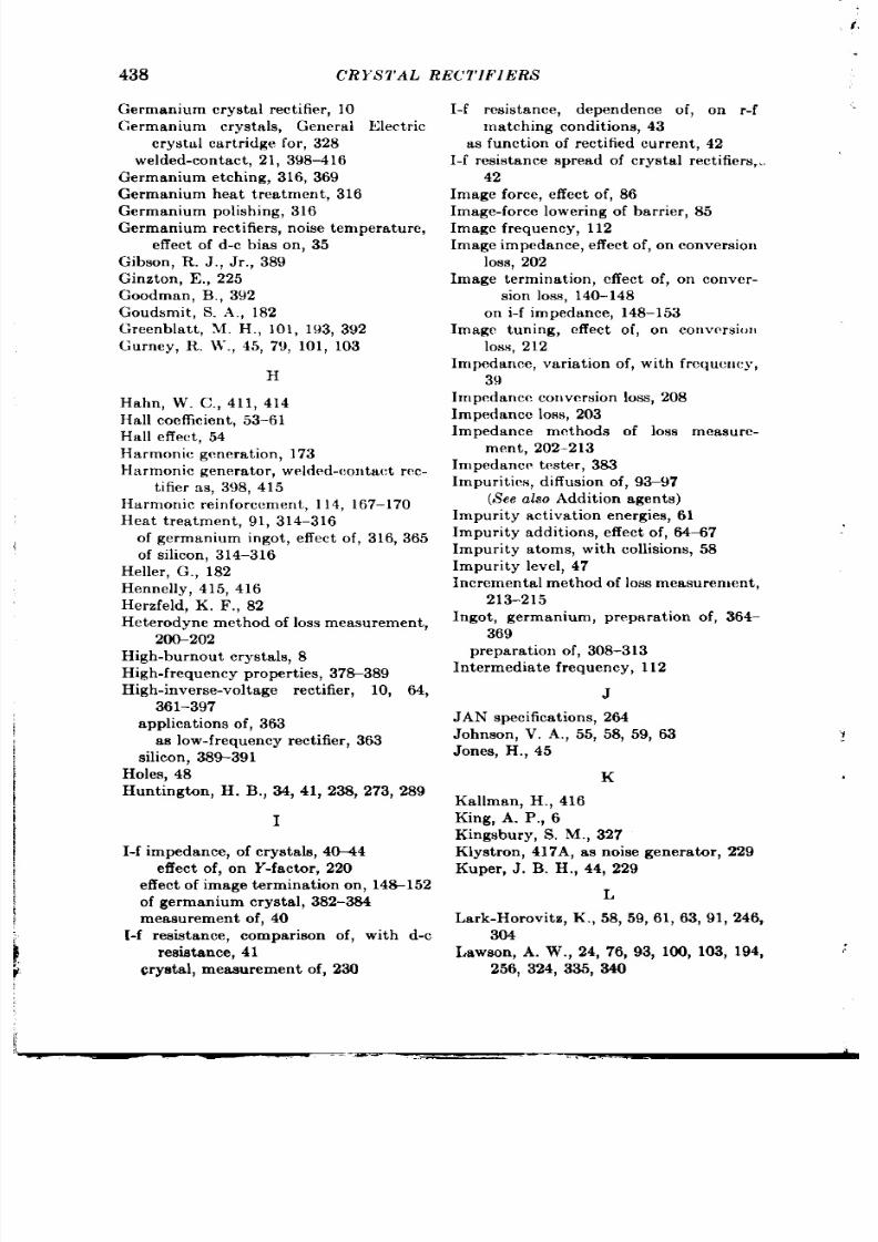
438
CR YS TAL R ECT I1’Ih ’R S
Germanium crys tu l r ect ifier , 10
Germa nium cryst ls, Gener al E lect r ic
cr ys tu l ca r t rid ge for , 328
welded-contact , 21, 398–416
German ium et ch in g, 316, 369
Germa nium h ea t t rea tm en t, 316
Germanium polis hing, 316
German ium rect ifie rs , nois e t empera tu r e,
effect of d-c hiss on , 35
Gibson , R. J ., J r ,, 389
Gin zt on , E ., 225
Goodm an , B., 392
Gou dsm it , S. .\ ., 182
Gr een bla tt , M. H ., 101, 193,392
Gur ney, R. \ V., 45, 79, 101, 103
H
Hahn , W. C.,411,414
Hall coefficient , 53-61
Ha ll e ffe ct , 54
Ha rmon ic gen er a t ion , 173
Harmon ic gene ra tor , welded -con twct r r c-
t ifier a s, 398, 415
Harmon ic r e in for cemen t , 114, 167-170
Hea t t r ea tmen t, 91, 314-316
of german ium in got , effect of, 316, 365
of sil icon, 314–316
Heller , G., 182
Hennelly, 415, 416
H er zfeld, K. F., 82
Het er odyne met hod of los s mea su r emen t ,
20&202
H igh -bu r nou t cr yst a ls, 8
High-frequency proper t i es , 37S389
H igh -in ver se-volt age r ect ifier , 10, 64,
361-397
applica t ion s of, 363
as low-fr equency rect ifie r , 363
silicon, 389-391
Holes , 48
H unt ingt on , H. B., 34, 41, 238, 273, 289
I
I -f impedance , of cr yst a ls , 4044
effect of, on Y-fa ct or , 220
e ffect of image t .e rmina t ion on , 14=152
of ge rman ium crys ta l, 382–384
mea su remen t of, 40
[-f resistance, compar ison of, with d-c
r es is tance , 41
crystal,measurementof, 230
I -f r esist an ce,
dependence of, nn r -f
ma tch ing condit ion s, 43
a s fu nct ion of r ect ified cu rr en t, 42
I -f r es is ta n ce s pr ead of cr yst a l r ect ifier s,,,
42
Image for ce, effect of, 86
Image-for ce lower ing of ba r r ier , 85
Image fr equ en cy, 112
Image impedance , e ffect of, on conve r sion
10ss, 202
Image termination, effect of, on conver-
sion loss, 40-148
on i-f impedance, 148–153
Image tuning, effect of, on con vcr sio]]
loss, 212
Impedance, va r ia t ion of, wit h fr equ cu cy,
39
I rupedancc conve r sion los s, 208
Impedance loss , 203
Impedance methods of loss measure-
ment , 202–213
Impeda n ce t est er , 383
Impur it ie s, d iffu s ion of, 93-97
(See a lso Addit ion agent s )
Impur it y a ct iva t ion ene rgies , 61
Impur it y a dd it ion s, e ffect of, M-67
Impu rit y a tom s, wit h collision s, 58
Impu rit y level, 47
Incr ement a l method of los s measu rement ,
213-215
In got , germa nium, pr epa ra tion of, 364-
369
p repa ra t ion of, 308-313
I nt ermed ia t e fr equ ency, 112
J
JAN specifica t ions, 264
J ohnson , V. A., 55, 58, 59, 63
J on es, H ., 45
K
Ka llm an , H ., 416
King, A. P., 6
Kin gsbu ry, S. M., 327
Klyst r on , 417A, a s n ois e gen er a tor , 229
Kuper , J . B. H., 44, 229
L
La r k-Hor ovit z, K., 58, 59, 61, 63,91, 246,
304
Lawson, A. W., 24, 76, 93, 100, 103, 194,
256, 324, 335, 340
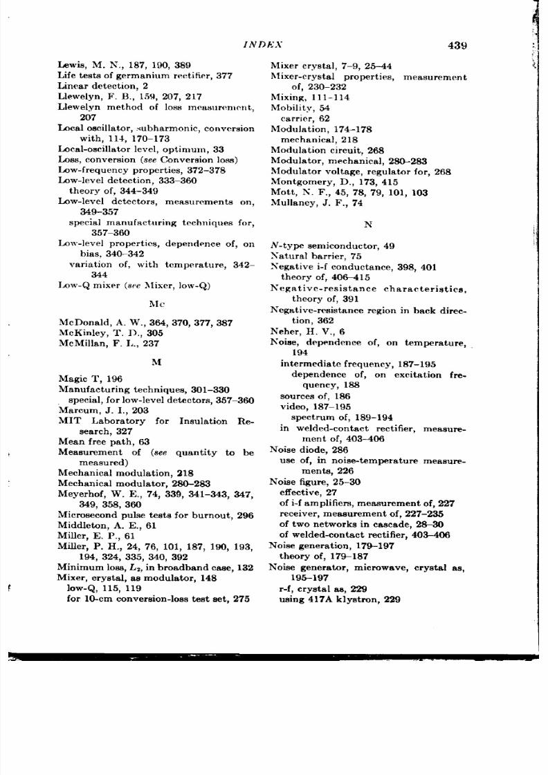
lNl)b;X
439
Lewis, M. N., 187, 190, 389
Life tests of germanium rectifier, 377
Linear de ection, 2
Llewelyn, F, B., 15!4, 207, 217
Llewelyn method of loss mcasurwnent,
207
Local osc llator, subharmonic, conversion
with, 114 , 170–173
Local-oscilla tor level, opt imum, 33
Loss, con v r sion (see Con ver sion loss)
Low-fr equ en cy pr oper ties, 372-378
Low-level det ect ion , 333–360
t heor y of, 344-349
Low-level det ectors, measurements on ,
349-357
specia l manufactu r ing techniques for ,
357-360
Lew-level proper t ies, dependence of, on
b ia s , 340–342
var ia t ion of, with t empera ture, 342–
344
Imw-Q mixe r (s ee llixer , 10W.Q)
ifc
McDona ld , A. W., 364, 370,377,387
McKinley, T. ., 305
M
Magic T, 196
Manufactu r ing t echn iques , 301-330
special, for low-level detectors , 357–36o
Ma rcum , J . 1,, 203
MIT Labora tory for Insula t ion Re.
sea rch , 327
Mea n fr ee pa th , 63
Measurement of (see quantity to be
measured)
Mechanica l modula t ion , 218
Mechan ica l modu la tor , 280-283
Meyer hof, W. E ., 74, 339, 341-343, 347,
349, 358, 60
Micr osecond pu lse t est s for bu rn ou t, 296
Middlebn , A. E., 61
Miller , E. P ., 61
Miller , P . H., 24, 76, 101, 187, 190, 193,
194, 324, 335, 340, 392
Min imum loss, L*, in br oa dba n d ca se, 132
Mixer , cr yst al, a s modu la t or , 148
low-Q, 115, 119
for lo-cm conver sion -loss t est set , 275
Mixer cr yst a l, 7-9, 25--44
h fixcr -cr yst a l pr oper ties, mea su remen t
of, 230–232
hlixing, 111-114
Mobilit y, 54
ca r r ie r, 62
i llodulat ion, 174–178
mechan ica l, 218
Modula t ion cir cu it , 268
Modula tor , mechan ica l, 2t ?&283
h lodu la t r volt age, r egu la t or for , 268
Mon tgomer y, D., 173, 415
Mott , N. F ,, 45, 78, 79, 101, 103
Mulla ney, J . F., 74
N
N-t ype s em iconduct or , 49
A’a tu ral ba r r ier , 75
Nega t ive i-f con du ct a nce, 398, 401
t h eor y of, 406415
Nega tive-r esist an ce ch ar act er ist ics,
t heor y of, 391
N’cgat ive-rc.s is tance region in back direc.
t ion , 362
Neher , H. V., 6
Noise, depen den ce of, on t em per at ur e,
194
in te rmedia te frequency, 187–195
dependence of, on excita t ion fr e-
quency, 188
sources
of,
186
video, 187–195
spect rum of, 189-194
in welded-con ta ct r ect ifier , m ea su re-
men t of, 403406
Nois e d iode, 286
u se of, i n oise-t emper at ur e m ea su re-
men ts, 226
Noise figure , 25-30
effect ive, 27
f i-f amplifier s+measu remen t of, 227
rece ive r , measu remen t of, 227–235
f two n etwor ks in ca sca de, 2tX30
f welded-contact rect ifie r , 403-406
Noise genera t ion , 179-197
t h eor y of, 7%187
Noise gen er at or , m icr owa ve, cr yst al a s,
195-197
r -f, cr y t al a a, 229
u sin g 417A k lyst ron , 229

440
CRYS TAL RECTIFIERS
Noise m ea sur ing set , for &m band, 283-
289
ca libr a tion of, 288
oper a tion of, 288
for 10-cm band, 289-292
Noise t emper at ur e, 30, 179
dependence of, in fr equency, 188-194
a s fu nct ion of r -f t un in g, 232–235
as fun ct ion of sign al a nd im age r eflec-
t ion , 234
mea su r emen t of, 21%235
r an ge of, in pr odu ct ion units, 32
h ,oise-t emPer at ur e a ppa ra tu s, ca libr at ion
of. 227
Noise-temper ature depen dence on am-
bient tempera ture, ca lcu la ted a nd
obse rved, 95
Noise-t empera tu re measuremen t , of l-cm
rect l ficrs , 292
u sirm nois e d iode. 226
Nois e t est s et s, st a rida r d, 283–293
Non lin ea r elemen t, 1
Non lin ea r r es is ta n ce of ba r rier , 24
Non linea r r es is tance ma t r ix, 153–157
Nordh eim, L. W., 77
Nor th, H. Q., 11, 21, 35, 128, 173, 304,
308, 313, 314, 317, 328, 398, 399,
403, 406, 411, 414-416
Nyqu ist , H., 181
0
oscillator mount, 266
Output circuit, of l-cm conver sion -los s
t est set , 278
Ou tpu t -met er cir cu it , 287
Ou tpu t nOise r at io, 30
(See Noise t empera tu re)
Ou tpu t r es st an ce, dyn amic, 333
P
P -t ype sem icondu ct or , 49
P ar asit ic im peda nces, effect of, on con -
version loss, 157–163
P ar asit ic, 112
P~ternack, S., 75
P ea k in ver se volt age, 362, 375
dependence of, on fr equency, 38G 82
Pea r sa ll, C. S., 91, 307, 308, 314, 318,392
P ea rson , G. L., 193
P en et ra tion of ba rr ier , effect of, 85, 87
l’enn sylvan ia , Univer sit y of, 8, 24, 61, 75,
76, 93, 100, 101, 103, 187, 190, 193,
194,256, 263, 307, 319, 324, 335, 339,
340, 341, 343, 354, 357, 358, 363,
389, 391, 392
P et er son , L. C,, 159, 217
P fa nn , W. G., 92, 318-320
Phenomenologica l t h eory of conver sion ,
119-152
P hosph or us, a s a ddit ion a gen t, 67
Photod iode, 394
Photoelect r ic effect s , inge rman il]m , 393-
397
in s ilicon , 392
I
Phot opeak , 395
Phot oswit ch , I nc., 273, 289
Pickar , P. B.,364,370,377,387
P igt a il ca r tr id ge, 18
Polishing, 314-316
P ou nd, R, V.,34, 174, 178,208
Pound met hod of loss mea su remen t, 20&
212
Powe ll, Virgin ia , 307, 314
Preamplifie r circu it , 287
Precau t ions, handling, 18-20
P r epar a tion of (s ee it em p repar ed )
9
P roduct ion t est ing method s, of los s mea s-
urement , 213–218
Product ion un it s, r ange of conve r sion los s
a nd n oise t em per at ur e in , 32
Purdue University , 10,41,55,61,80,82,
83, 87, 89, 119, 125, 135, 166, 185,
215, 304, 306, 361, 363-365, 368-372 ,
37&378 381-385,387,388,391,394,
396 , 398 , 399,429
Pur ifica t ion of (see it em purified)
R
v
Radiomet er , m icr owave, lg7
Rece ive r, crys ta l-video, 9
Reciprocity, 117, 124-128,203
exper imenta l t es ts of, 125-127
fu ll, 118, 124
wea k, 118, 124, 139, 203, 216
gener a l condit ion of, 124
Recip rocit y factor , 203
Recipr ocit y t heor em of Dick e, 125, 417-
420
Rect ifica t ion , bar r ie r -layer , 6%72
d iffu s ion theory of, 77-81
diode t h eor y of, 78, 81-82
1
efficiency of, 3
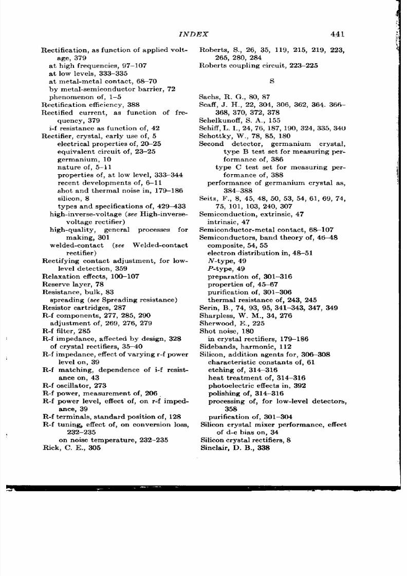
INDEX
441
Rect ifica t ion , a s funct ion of app lied volt -
a ge, 379
a t h igh fr equencies , 97–107
a t low levels , 333–335
a t m et a -m et al con ta ct , 6%70
by met al-sem icondu ct or ba r rier , 72
p hen omenon f, 1-5
Rect ifica t ion efficiency , 388
Rect ified cur r en t , as funct ion of fr e-
quency 379
i-f r esist an ce a s fu nct ion of, 42
Rect ifier , cr yst al, ea rly u se of, 5
e lect r ica l p roper t ie s of, 2&25
equ iva len t cir cu it of, 23-25
german ium , 10
n at ur e of, 5–11
pr oper ties of, a t low level, 333-344
r ecen t developm en ts of, &l 1
sh ot a nd t herma l n oise in , 179–186
s ilicon , 8
t ypes and specifica t ion s of, 429433
high-inverse-vol tage (see High-inverse-
vol tage rect i fier)
h igh-quality, genera l processes for
making, 301
welded -con ta ct (see Welded-con ta ct
rectifier)
Rect ifyin g con ta ct a dju stmen t, for low-
level d et ect ion , 359
Relaxa t ion effects , 100-107
Reser ve la yer , 78
Res ist a nce, bu lk , 83
spreading (see Spreading resis tance)
Resis tor ca r t r idges, 287
R-f compon en ts, 277, 285, 290
a dju stmen t of, 269, 276, 279
R-f filt er , 285
R-f impeda n ce, a ffect ed by design , 328
of cr ys ta l r ect ifier s, 3=0
R-f impedance , e ffe ct of va r ying r -f powe r
level on , 39
R-f m atching, depen den ce of i-f resist -
a nce on , 43
R-f oscilla tor , 273
R-f power , m ea su rem en t of, 206,
R-f power level, effect of, on r :f im ped-
a nce, 39
R -f t erm ina ls , st a ndar d pos it ion of, 128
R-f t un in g, effect of, on con ver sion lees,
232-235
on nois e t emper a t ur e, 232-235
Rick, C. E., 305
Rober ts, S., 26, 35, 119, 215, 219, 223,
265, 280, 284
Robe rt s coup l ng cir cu it , 223-225
s
Sachs, R. G., 80, 87
St aff, J . H ,, 22, 304, 306, 362, 364.366-
368, 370, 372, 378
Schelkunoff, S, A., 155
Sch iff, L. 1,,24,76, 187, 190, 324, 335, 34u
Sch ott ky, W., 78, 85, 180
Second detector , germanium crysta l,
t ype B test set for ea sur ing per -
forman ce of, 386
type C test set for m ea su rin g per -
formance of, 3 8 8
per forma nce of germa nium cr yst al a s,
3 8 4 - 3 8 8
Seitz, F., 8 , 4 5 , 4 8 , 5 0 , 5 3 , 5 4 , 6 1 , 6 9 , 7 4 ,
7 5 , 101, 103, 240, 307
Sem icon du ct ion , ext rin sic, 47
n tr in sic, 47
Sem icon du ct or -m et al con ta ct , 6%107
Semiconductors, band theory of, 4648
composit e, 54, 55
elect ron dist ribu tion in , 48-51
N-type, 49
P-type, 49
pr epa ra tion of, 301-316
pr oper ties of, 4$67
p ur ifica t ion of, 301–306
thermal resist ance of, 243, 245
Ser in , B., 74, 93, 95, 341–343, 347, 349
Sha rpless, W. M., 34, 276
Sherwood, E,, 225
Shot noise, 180
in cr yst al r ect ifier s, 179–186
Sidebands, ha rmonic, 112
Silicon , addit ion agen ts for , 30G308
cha ract er ist ic const an ts of, 61
et ch in g of, 314–316
heat t r ea tment of, 314-316
phot oelect ric effects in , 392
polis hin g of, 314-316
processin g of, for low-level det ector s,
358
pu rifica tion of, 30–304
Silicon cryst al mixer per forma nce, effect
of d-c bias on , 34
Silicon cr yst al r ect ifier s, 8
Sincla ir , D. B., 338
$.
,’
442
CR YS1’AL REC.’T I flA ’RS
Sk in effect a t m et a l-sem icon du ct or con -
tact , 421-426
Smith, A, H.,343,349,358
Smith, R. N.,41,77, 119, 125, 135, 146,
166, 185, 215, 364, 370, 377, 381,
382, 384,387,388
Smyt he, W, R,,249
Sou thwor t h, G. C.,6
Specia l t yp es , d evelopmen t of, !)-11
Specificat ions of crystal rect i fiers , 429-433
commen ts on , 429
Spen ke, E ., 78
S per r y Gyr oscop e Company, 225, 318
Sper r y Res ea r ch Labor a t or ies , 396
Spike, 237
and fla t , rela t ive impor tance of, in
bu rn ou t, 237
Spik e t est for bu rn ou t, 293-295
Spr eading r ea is ta n ce,24, 83
of ell p tica l con t act , 427
loca l, 88
Squ ar e law, 333
Squa re-law det ect ion , 3
S tabilit y, 1S20
S ta n co Dis tr ibu t or s, 325
St an da rd posit ion of r -f t ermin als, 128
Stephens, W. E., 24, 74, 76, 93, 95, 99,
187, 190, 194, 324, 335, 339, 340,
343, 349,358,389,392
St ever , H . Gu yfor d, 303
S tr u ct u re, of ba r r ier la yer , 70-77
Sum fr equ en cy, 112
Sur fa ce levels , 101, 107
Sur fa ce t r ea tmen t , 369
Sylvania Elect r ic P roducte Company,
323, 363, 387, 429
T
Taft , E ., 174
Ta ylor )J . H .,389
Terman, F. E .,3
Tes t equ ipmen t , 26K300
(See a fso qua nt ity m ea su red; com -
ponen t t es ted )
Th erma l n oise, in cr yst al r ect ifier s, 179-
186
Th erma l r ela xa t ion t im e, 254
Th erma l r esist an ce, of ca t wh isker , 243,
245
of s em iconduct or , 243, 245
‘r h eu er er , H . C., 9, 22, 304, 306, 307, 311,
326, 362, 364, 370, 372, 378
Torrey, H. C.,21, 163 ,292 ,392 ,408 ,413 ,
421
TRswitch , 129
Treut ing, R. C.,314,326
Tu ck er , 303
Tunin g, st an da rd fixed, 270
‘r unnele fect , 85, 87
Type B test set for measur ing over -a ll
p er formance of cr ys ta l s econd det ec-
t or s, 386
Type C test set for measur ing r ect ifica -
t ion effic ency of crysta l second
det ector s , 388
Typw of crys t al r ect ifie rs , 42%4 3
,
u
Un iform con t act pot en t ia l d iffe r ence , 400
University of Pennsylvan ia (s ee Pennsyl-
van ia , Univer sit y of)
v
Video cr yst al, 9
figu r e of mer it of, M4-347
t est equ ipm en t for pr odu ct ion t est in g
of, 352
Video-cr yst a l h older , wit h sin gle t un in g
adju stmen t for 1N30 r ?ct ifier e, 354
Video res is t ance , 333
equipment for measur ement of, 349–
357
methods of measurement of, 349-357
Volt a ge-br eakdown hypot h es is , in bu r u-
ou t 240
von H ippel, A., 327
~
Vou gh t, R. H ., 341, 342, 347
w
Wa ler st ein , I., 61
Waltz M. C., 44, 229, 401, 403
Weiss, P . R., 182
Weia ekopf, V. F ., 58, 87, 179, 182, 186
Weld ed -con t a ct germanium crys ta ls, 21,
39&416
Welded -con t act r ect ifie rs , 11, 329
applica t ions of, 415
1
cons t ruct ion of, 398-400
gener a l p rop er t ies of, 400

INDEX
Welded-con ta ct r ect ifier s, a s gen er at or
of m illim et er r adia tion , 398
a a h armon ic gen er at or s, 398, 415
measuremen t of qoise in , 403–406
noise figure of, 403-406
Welded con ta ct s, 99, 254
Weseon , L. G,, 327
Western E lect r ic Company, 270,318,323
Wes tinghou se Resea r ch Labor a tor y, 203,
307, 315, 321
Wh aley, R. M., 364, 368, 370, 377, 387
Whisker , ca t , 316-323
fabrica t ion of, 31*322
for low-leve l det ector s , 359
mount in g of, 321
Wh isker ma ter ia ls, 316
Wh isker poin t , form ing of, 318-320
Wh isker sh ape, 320
443
Whitm er , C. A., 35, 276
Wiesn er , J . B., 237
Wilson, A. H., 45, 49, 77
Woodya rd, J , R., 318, 396
Work funct ions, 51-53
fluctua tions in , 86
Y
Y-factor , 31
a s fu nct ion of i-f impeda nce of cr yst al,
220
Year ian, H. J ., 83, 87, 89, 364, 370, 377,
378, 380, 381, 382, 384, 387
z
Zen er , C., 46