Embed Size (px)
Citation preview

AE0.21EFUJITSU SEMICONDUCTORDATA SHEET
FLASH MEMORYCMOS
64 M (4M ×××× 16) BITMirrorFlash TM
MBM29PL65LM 90/10
nnnn DESCRIPTIONThe MBM29PL65LM is a 64M-bit, 3.0 V-only Flash memory organized as 4M words by 16 bits. The MBM29PL65LM is offered in a 48-pin TSOP(I). The device is designed to be programmed in-system with the standard 3.0 V VCC supply. 12.0 V VPP and 5.0 V VCC are not required for write or erase operations. The devices can also be reprogrammed in standard EPROM programmers.
The standard MBM29PL65LM offers access times of 90 ns, allowing operation of high-speed microprocessors without wait states. To eliminate bus contention the devices have separate chip enable (CE), write enable (WE), and output enable (OE) controls.
nnnn PRODUCT LINE UP
nnnn PACKAGE
Part No. MBM29PL65LM90 MBM29PL65LM10
VCC 3.0V to 3.6V 3.0V to 3.6V
VCCQ VCC VCC
Max. Address Access Time 90 ns 100 ns
Max. CE Access Time 90 ns 100 ns
Max. Page Read Access Time 25 ns 30 ns
(FPT-48P-M19)
48-pin plastic TSOP(I)
Marking Side
1This document contains information on product under development at Fujitsu. The information is intended to help you evaluate this product. Fujitsu reserves theright to change this proposed product without notice.
2
MBM29PL65LM 90/10
The MBM29PL65LM supports command set compatible with JEDEC single-power-supply EEPROMS standard. Commands are written into the command register. The register contents serve as input to an internal state-machine which controls the erase and programming circuitry. Write cycles also internally latch addresses and data needed for the programming and erase operations. Reading data out of the devices is similar to reading from 5.0 V and 12.0 V Flash or EPROM devices.
The MBM29PL65LM is programmed by executing the program command sequence. This will invoke the Embedded Program AlgorithmTM which is an internal algorithm that automatically times the program pulse widths and verifies proper cell margin. Typically, each sector can be programmed and verified in about 0.1 seconds. Erase is accomplished by executing the erase command sequence. This will invoke the Embedded Erase AlgorithmTM which is an internal algorithm that automatically preprograms the array if it is not already programmed before executing the erase operation. During erase, the device automatically times the erase pulse widths and verifies proper cell margin.
Each sector is typically erased and verified in 1.0 second. (If already completely preprogrammed.)
The device also features a sector erase architecture. The sector mode allows each sector to be erased and reprogrammed without affecting other sectors. All sectors are erased when shipped from the factory.
The device features single 3.0 V power supply operation for both read and write functions. Internally generated and regulated voltages are provided for the program and erase operations. A low VCC detector automatically inhibits write operations on the loss of power. The end of program or erase is detected by Data Polling of DQ7, by the Toggle Bit feature on DQ6. Once the end of a program or erase cycle has been completed, the devices internally return to the read mode.
The Enhanced VCCQ feature allows the output voltage generated on the device to be determined based on the VCCQ level. This feature also allows this device to tolerate the same driving and receiving signals from other 3V devices on the same bus.
Fujitsu Flash technology combines years of Flash memory manufacturing experience to produce the highest levels of quality, reliability, and cost effectiveness. The devices electrically erase all bits within a sector simultaneously via hot-hole assisted erase. The words are programmed one word at a time using the EPROM programming mechanism of hot electron injection.
(AE0.21E) Advance Info.

MBM29PL65LM 90/10
nnnn FEATURES• 0.23 µµµµm Process Technology• Single 3.0 V read, program and erase
Minimizes system level power requirements• Industry-standard pinouts
48-pin TSOP (I) (Package suffix: TN - Normal Bend Type)• Minimum 100,000 program/erase cycles• High performance Page mode
Fast 4 words access capablilty• Sector erase architecture
One hundred twenty-eight 32K words sectorsAny combination of sectors can be concurrently erased. Also supports full chip erase
• HiddenROM (Hi-ROM) 128 words of Hi-ROM, accessible through a “Hi-ROM Entry” command sequenceFactory serialized and protected to provide a secure electronic serial number (ESN)
• WP input pinAt VIL, allows protection of first 32K words sector, regardless of sector protection/unprotection statusAt VIH, allows removal of protection
• ACC input pinAt VACC, increases program performance
• Embedded Erase TM AlgorithmsAutomatically pre-programs and erases the chip or any sector
• Embedded Program TM AlgorithmsAutomatically writes and verifies data at specified address
• Data Polling and Toggle Bit feature for detection of program or erase cycle completion• Automatic sleep mode
When addresses remain stable, automatically switches themselves to low power mode• Program Suspend/Resume
Suspends the program operation to allow a read in another address• Low V CC write inhibit ≤ 2.5 V• Erase Suspend/Resume
Suspends the erase operation to allow a read data and/or program in another sector within the same device• Sector Group Protection
Hardware method disables any combination of sector groups from program or erase operations• Sector Group Protection Set function by Extended sector protect command• Fast Programming Function by Extended Command• Temporary sector group unprotection
Temporary sector group unprotection via the RESET pinThis feature allows code changes in previously locked sectors
• In accordance with CFI (C ommon F lash Memory I nterface)
Embedded EraseTM and Embedded ProgramTM are trademarks of Advanced Micro Devices, Inc.MirrorFlashTM and HiddenROMTM are trademarks of Fujitsu Limited.
Advance Info. (AE0.21E) 3
4
MBM29PL65LM 90/10
nnnn PIN ASSIGNMENTS
nnnn PIN DESCRIPTIONS
Table 1 MBM29PL65LM Pin Configuration
Pin Function
A21 to A0 Address Inputs
DQ15 to DQ0 Data Inputs/Outputs
CE Chip Enable
OE Output Enable
WE Write Enable
WP Hardware Write Protection
ACC Program Acceleration
RESET Hardware Reset Pin/Temporary Sector Group Unprotection
VCC Device Power Supply
VCCQ Output Buffer Power Supply
VSS Device Ground
A15
A14
A13
A12
A11
A10
A9
A8
A21
A20
WERESET
ACCWPA19
A18
A17
A7
A6
A5
A4
A3
A2
A1
123456789101112131415161718192021222324
484746454443424140393837363534333231302928272625
TSOP(I)
A16
VCCQ
VSS
DQ15
DQ7
DQ14
DQ6
DQ13
DQ5
DQ12
DQ4
VCC
DQ11
DQ3
DQ10
DQ2
DQ9
DQ1
DQ8
DQ0
OEVSS
CEA0
(Marking Side)
FPT-48P-M19
(AE0.21E) Advance Info.

MBM29PL65LM 90/10
nnnn BLOCK DIAGRAM
nnnn LOGIC SYMBOL
VSS
VCC
WE
CE
A1, A0
OE
Erase VoltageGenerator
DQ15 to DQ0
StateControl
CommandRegister
Program VoltageGenerator
AddressLatch
X-Decoder
Y-Decoder
Cell Matrix
Y-Gating
Chip EnableOutput Enable
Logic
Data Latch
STB
STB
RESET
WP
Timer forProgram/Erase
VCCQ
Input/OutputBuffers
A21 to A2
ACC
22
A21 to A0
WE
OE
CE
DQ 15 to DQ 0
RESET
WP
ACC
16
Advance Info. (AE0.21E) 5

6
MBM29PL65LM 90/10
nnnn DEVICE BUS OPERATION
(Continued)Legend: L = VIL, H = VIH, X = VIL or VIH. See DC Characteristics for voltage levels.
Hi-Z = High-Z, VID = 11.5 to 12.5V
Notes: *1. Manufacturer and device codes may also be accessed via a command register write sequence. See Table 3.
*2. Refer to Sector Group Protection.*3. Protects the first 32K words sector (SA0)*4. DIN or DOUT as required by command sequence, data polling, or sector protect algorithm*5. If WP = VIL, the first sector remains protected.
If WP = VIH, the first sector will be protected or unprotected as determined by the method specified in"Sector Group Protection" in page 19.
Table 2 MBM29PL65LM User Bus Operations
Operation CE OE WE A0 A1 A2 A3 A6 A9DQ0 toDQ15
RESET WP
Standby H X X X X X X X X Hi-Z H X
Autoselect Manufacture Code *1 L L H L L L L L VID Code H X
Autoselect Device Code *1 L L H H L L L L VID Code H X
Read L L H A0 A1 A2 A3 A6 A9 DOUT H X
Output Disable L H H X X X X X X Hi-Z H X
Write (Program/Erase) L H L A0 A1 A2 A3 A6 A9 *4 H *5
Enable Sector Group Protection *2 L H L L H L L L X *4 VID H
Sector Group Unprotection *2 L H L L H L L H X *4 VID H
Temporary Sector Group Unprotection X X X X X X X X X *4 VID H
Reset (Hardware) X X X X X X X X X Hi-Z L X
Sector Write Protection *3 X X X X X X X X X X H L
(AE0.21E) Advance Info.

MBM29PL65LM 90/10
usycle
a
Reset —
Reset —
Autos —
Progra —
Chip E 10h
Secto 30h
Progra —
Progra —
Set to —
Fast P —
Reset —
Write PD
Progra —
Write —
ExtenProtec
—
Query —
Hi-RO —
Hi-RO —
Hi-RO —
Legend: Address bits A21 to A11 = X = “H” or “L” for all address commands except for Program Address (PA),Sector Address (SA) and Sector Group Address (SGA).Bus operations are defined in Tables 2.RA = Address of the memory location to be read.PA = Address of the memory location to be programmed. Addresses are latched on the falling edge
of the write pulse.SA = Address of the sector to be programmed / erased. The combination of A21, A20, A19, A18, A17, A16
and A15 will uniquely select any sector. See Table 5.SGA = Sector Group Address to be protected. See Table 6. RD = Data read from location RA during read operation.PD = Data to be programmed at location PA. Data is latched on the rising edge of write plus.WBL = Write Buffer LocationHRA = Address of the HiddenROM area : 000000h to 00007Fh
Table 3 MBM29PL65LM Standard Command Definitions (Note*1)
CommandSequence
BusWrite Cycle
s Req'd
First BusWrite Cycle
Second BusWrite Cycle
Third BusWrite Cycle
Fourth BusRead/Write
CycleFifth Bus
Write CycleSixth B
Write C
Addr Data Addr Data Addr Data Addr Data Addr Data Addr Dat
*2 1 XXXh F0h — — — — — — — — —
*2 3 555h AAh 2AAh 55h 555h F0h — — — — —
elect(Device ID) 4 555h AAh 2AAh 55h 555h 90h 00h 04h — — —
m 4 555h AAh 2AAh 55h 555h A0h PA PD — — —
rase 6 555h AAh 2AAh 55h 555h 80h 555h AAh 2AAh 55h 555h
r Erase 6 555h AAh 2AAh 55h 555h 80h 555h AAh 2AAh 55h SA
m/Erase Suspend*3 1 BAh B0h — — — — — — — — —
m/Erase Resume*3 1 BAh 30h — — — — — — — — —
Fast Mode*4 3 555h AAh 2AAh 55h 555h 20h — — — — —
rogram *4 2 XXXh A0h PA PD — — — — — — —
from Fast Mode *5 2 XXXh 90h XXXh 00h*12 — — — — — — —
to Buffer 20 555h AAh 2AAh 55h SA 25h SA 0Fh PA PD WBL
m Buffer to Flash (Confirm) 1 SA 29h — — — — — — — — —
to Buffer Abort Reset*6 3 555h AAh 2AAh 55h XXXh F0h — — — — —
ded Sector Group tion *7,*8
4 XXXh 60h SGA 60h SGA 40h SGA SD — — —
*9 1 55h 98h — — — — — — — — —
M Entry*10 3 555h AAh 2AAh 55h 555h 88h — — — — —
M Program *10,*11 4 555h AAh 2AAh 55h 555h A0h PA PD — — —
M Exit *11 4 555h AAh 2AAh 55h 555h 90h XXXh 00h — — —
Advance Info. (AE0.21E) 7
8
MBM29PL65LM 90/10
Notes: *1. The command combinations not described in Table 3 are illegal.*2. Both of these reset commands are equivalent except for "Write to Buffer Abort" reset.*3. The Erase Suspend and Erase Resume command are valid only during a sector erase operation.*4. The Set to Fast Mode command is required prior to the Fast Program command.*5. The Reset from Fast Mode command is required to return to the read mode when the device is in
fast mode.*6. Reset to the read mode. The Write to Buffer Abert Reset command is required after the Write to
Buffer operation was aborted.*7. This command is valid while RESET = VID.*8. Sector Group Address (SGA) with A6 = 0, A3 = 0, A2 = 0, A1 = 1, and A0 = 0*9. The valid address are A6 to A0.*10.The HiddenROM Entry command is required prior to the HiddenROM programming.*11.This command is valid during HiddenROM mode.*12.The data “F0h” is also acceptable.
(AE0.21E) Advance Info.

MBM29PL65LM 90/10
Notes: *1. At Word mode, a read cycle at address01h outputs device code. When 227Eh is output, it indicates that reading two additional codes, called Extended Device Codes, will be required. Therefore the system may continue reading out these Extended Device Codes at the address of 0Eh, as well as at 0Fh.
*2. Outputs 01h at protected sector group addresses and outputs 00h at unprotected sector group addresses.
Table 4 Sector Group Protection Verify Autoselect Codes
Type A 21 to A 12 A6 A3 A2 A1 A0 Code (HEX)
Manufacturer’s Code X VIL VIL VIL VIL VIL 04h
Device Code X VIL VIL VIL VIL VIH 227Eh
Extended Device Code*1X VIL VIH VIH VIH VIL 2213h
X VIL VIH VIH VIH VIH 2201h
Sector Group Protection Sector GroupAddresses VIL VIL VIL VIH VIL *2
Advance Info. (AE0.21E) 9
10
MBM29PL65LM 90/10
(Continued)
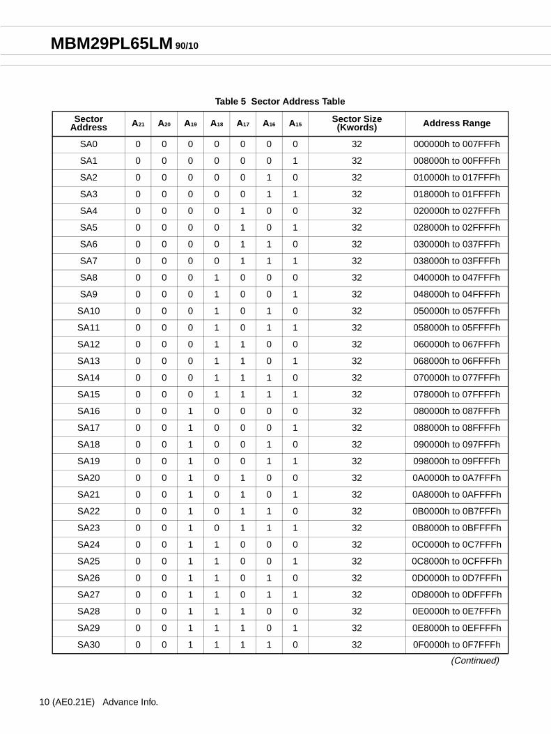
Table 5 Sector Address Table
SectorAddress A21 A20 A19 A18 A17 A16 A15
Sector Size(Kwords) Address Range
SA0 0 0 0 0 0 0 0 32 000000h to 007FFFh
SA1 0 0 0 0 0 0 1 32 008000h to 00FFFFh
SA2 0 0 0 0 0 1 0 32 010000h to 017FFFh
SA3 0 0 0 0 0 1 1 32 018000h to 01FFFFh
SA4 0 0 0 0 1 0 0 32 020000h to 027FFFh
SA5 0 0 0 0 1 0 1 32 028000h to 02FFFFh
SA6 0 0 0 0 1 1 0 32 030000h to 037FFFh
SA7 0 0 0 0 1 1 1 32 038000h to 03FFFFh
SA8 0 0 0 1 0 0 0 32 040000h to 047FFFh
SA9 0 0 0 1 0 0 1 32 048000h to 04FFFFh
SA10 0 0 0 1 0 1 0 32 050000h to 057FFFh
SA11 0 0 0 1 0 1 1 32 058000h to 05FFFFh
SA12 0 0 0 1 1 0 0 32 060000h to 067FFFh
SA13 0 0 0 1 1 0 1 32 068000h to 06FFFFh
SA14 0 0 0 1 1 1 0 32 070000h to 077FFFh
SA15 0 0 0 1 1 1 1 32 078000h to 07FFFFh
SA16 0 0 1 0 0 0 0 32 080000h to 087FFFh
SA17 0 0 1 0 0 0 1 32 088000h to 08FFFFh
SA18 0 0 1 0 0 1 0 32 090000h to 097FFFh
SA19 0 0 1 0 0 1 1 32 098000h to 09FFFFh
SA20 0 0 1 0 1 0 0 32 0A0000h to 0A7FFFh
SA21 0 0 1 0 1 0 1 32 0A8000h to 0AFFFFh
SA22 0 0 1 0 1 1 0 32 0B0000h to 0B7FFFh
SA23 0 0 1 0 1 1 1 32 0B8000h to 0BFFFFh
SA24 0 0 1 1 0 0 0 32 0C0000h to 0C7FFFh
SA25 0 0 1 1 0 0 1 32 0C8000h to 0CFFFFh
SA26 0 0 1 1 0 1 0 32 0D0000h to 0D7FFFh
SA27 0 0 1 1 0 1 1 32 0D8000h to 0DFFFFh
SA28 0 0 1 1 1 0 0 32 0E0000h to 0E7FFFh
SA29 0 0 1 1 1 0 1 32 0E8000h to 0EFFFFh
SA30 0 0 1 1 1 1 0 32 0F0000h to 0F7FFFh
(AE0.21E) Advance Info.
MBM29PL65LM 90/10
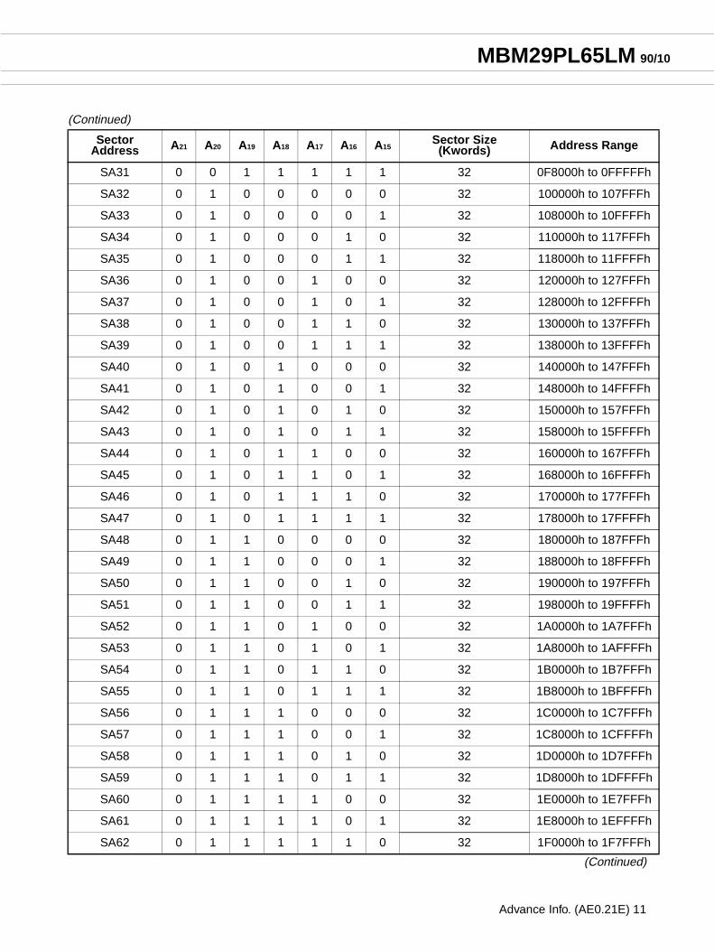
(Continued)
(Continued)
SectorAddress A21 A20 A19 A18 A17 A16 A15
Sector Size(Kwords) Address Range
SA31 0 0 1 1 1 1 1 32 0F8000h to 0FFFFFh
SA32 0 1 0 0 0 0 0 32 100000h to 107FFFh
SA33 0 1 0 0 0 0 1 32 108000h to 10FFFFh
SA34 0 1 0 0 0 1 0 32 110000h to 117FFFh
SA35 0 1 0 0 0 1 1 32 118000h to 11FFFFh
SA36 0 1 0 0 1 0 0 32 120000h to 127FFFh
SA37 0 1 0 0 1 0 1 32 128000h to 12FFFFh
SA38 0 1 0 0 1 1 0 32 130000h to 137FFFh
SA39 0 1 0 0 1 1 1 32 138000h to 13FFFFh
SA40 0 1 0 1 0 0 0 32 140000h to 147FFFh
SA41 0 1 0 1 0 0 1 32 148000h to 14FFFFh
SA42 0 1 0 1 0 1 0 32 150000h to 157FFFh
SA43 0 1 0 1 0 1 1 32 158000h to 15FFFFh
SA44 0 1 0 1 1 0 0 32 160000h to 167FFFh
SA45 0 1 0 1 1 0 1 32 168000h to 16FFFFh
SA46 0 1 0 1 1 1 0 32 170000h to 177FFFh
SA47 0 1 0 1 1 1 1 32 178000h to 17FFFFh
SA48 0 1 1 0 0 0 0 32 180000h to 187FFFh
SA49 0 1 1 0 0 0 1 32 188000h to 18FFFFh
SA50 0 1 1 0 0 1 0 32 190000h to 197FFFh
SA51 0 1 1 0 0 1 1 32 198000h to 19FFFFh
SA52 0 1 1 0 1 0 0 32 1A0000h to 1A7FFFh
SA53 0 1 1 0 1 0 1 32 1A8000h to 1AFFFFh
SA54 0 1 1 0 1 1 0 32 1B0000h to 1B7FFFh
SA55 0 1 1 0 1 1 1 32 1B8000h to 1BFFFFh
SA56 0 1 1 1 0 0 0 32 1C0000h to 1C7FFFh
SA57 0 1 1 1 0 0 1 32 1C8000h to 1CFFFFh
SA58 0 1 1 1 0 1 0 32 1D0000h to 1D7FFFh
SA59 0 1 1 1 0 1 1 32 1D8000h to 1DFFFFh
SA60 0 1 1 1 1 0 0 32 1E0000h to 1E7FFFh
SA61 0 1 1 1 1 0 1 32 1E8000h to 1EFFFFh
SA62 0 1 1 1 1 1 0 32 1F0000h to 1F7FFFh
Advance Info. (AE0.21E) 11
12
MBM29PL65LM 90/10
(Continued)
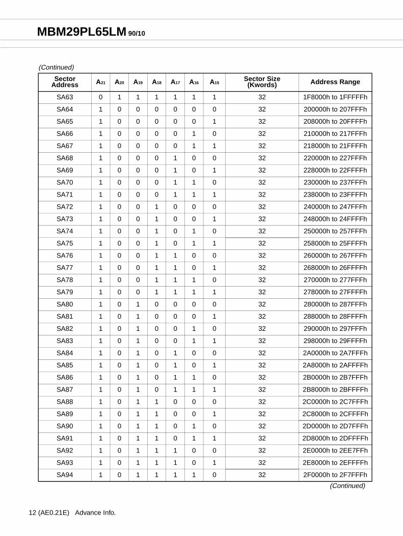
(Continued)
SectorAddress A21 A20 A19 A18 A17 A16 A15
Sector Size(Kwords) Address Range
SA63 0 1 1 1 1 1 1 32 1F8000h to 1FFFFFh
SA64 1 0 0 0 0 0 0 32 200000h to 207FFFh
SA65 1 0 0 0 0 0 1 32 208000h to 20FFFFh
SA66 1 0 0 0 0 1 0 32 210000h to 217FFFh
SA67 1 0 0 0 0 1 1 32 218000h to 21FFFFh
SA68 1 0 0 0 1 0 0 32 220000h to 227FFFh
SA69 1 0 0 0 1 0 1 32 228000h to 22FFFFh
SA70 1 0 0 0 1 1 0 32 230000h to 237FFFh
SA71 1 0 0 0 1 1 1 32 238000h to 23FFFFh
SA72 1 0 0 1 0 0 0 32 240000h to 247FFFh
SA73 1 0 0 1 0 0 1 32 248000h to 24FFFFh
SA74 1 0 0 1 0 1 0 32 250000h to 257FFFh
SA75 1 0 0 1 0 1 1 32 258000h to 25FFFFh
SA76 1 0 0 1 1 0 0 32 260000h to 267FFFh
SA77 1 0 0 1 1 0 1 32 268000h to 26FFFFh
SA78 1 0 0 1 1 1 0 32 270000h to 277FFFh
SA79 1 0 0 1 1 1 1 32 278000h to 27FFFFh
SA80 1 0 1 0 0 0 0 32 280000h to 287FFFh
SA81 1 0 1 0 0 0 1 32 288000h to 28FFFFh
SA82 1 0 1 0 0 1 0 32 290000h to 297FFFh
SA83 1 0 1 0 0 1 1 32 298000h to 29FFFFh
SA84 1 0 1 0 1 0 0 32 2A0000h to 2A7FFFh
SA85 1 0 1 0 1 0 1 32 2A8000h to 2AFFFFh
SA86 1 0 1 0 1 1 0 32 2B0000h to 2B7FFFh
SA87 1 0 1 0 1 1 1 32 2B8000h to 2BFFFFh
SA88 1 0 1 1 0 0 0 32 2C0000h to 2C7FFFh
SA89 1 0 1 1 0 0 1 32 2C8000h to 2CFFFFh
SA90 1 0 1 1 0 1 0 32 2D0000h to 2D7FFFh
SA91 1 0 1 1 0 1 1 32 2D8000h to 2DFFFFh
SA92 1 0 1 1 1 0 0 32 2E0000h to 2EE7FFh
SA93 1 0 1 1 1 0 1 32 2E8000h to 2EFFFFh
SA94 1 0 1 1 1 1 0 32 2F0000h to 2F7FFFh
(AE0.21E) Advance Info.

MBM29PL65LM 90/10
(Continued)
(Continued)
SectorAddress A21 A20 A19 A18 A17 A16 A15
Sector Size(Kwords) Address Range
SA95 1 0 1 1 1 1 1 32 2F8000h to 2FFFFFh
SA96 1 1 0 0 0 0 0 32 300000h to 307FFFh
SA97 1 1 0 0 0 0 1 32 308000h to 30FFFFh
SA98 1 1 0 0 0 1 0 32 310000h to 317FFFh
SA99 1 1 0 0 0 1 1 32 318000h to 31FFFFh
SA100 1 1 0 0 1 0 0 32 320000h to 327FFFh
SA101 1 1 0 0 1 0 1 32 328000h to 32FFFFh
SA102 1 1 0 0 1 1 0 32 330000h to 337FFFh
SA103 1 1 0 0 1 1 1 32 338000h to 33FFFFh
SA104 1 1 0 1 0 0 0 32 340000h to 347FFFh
SA105 1 1 0 1 0 0 1 32 348000h to 34FFFFh
SA106 1 1 0 1 0 1 0 32 350000h to 357FFFh
SA107 1 1 0 1 0 1 1 32 358000h to 35FFFFh
SA108 1 1 0 1 1 0 0 32 360000h to 367FFFh
SA109 1 1 0 1 1 0 1 32 368000h to 36FFFFh
SA110 1 1 0 1 1 1 0 32 370000h to 377FFFh
SA111 1 1 0 1 1 1 1 32 378000h to 37FFFFh
SA112 1 1 1 0 0 0 0 32 380000h to 387FFFh
SA113 1 1 1 0 0 0 1 32 388000h to 38FFFFh
SA114 1 1 1 0 0 1 0 32 390000h to 397FFFh
SA115 1 1 1 0 0 1 1 32 398000h to 39FFFFh
SA116 1 1 1 0 1 0 0 32 3A0000h to 3A7FFFh
SA117 1 1 1 0 1 0 1 32 3A8000h to 3AFFFFh
SA118 1 1 1 0 1 1 0 32 3B0000h to 3B7FFFh
SA119 1 1 1 0 1 1 1 32 3B8000h to 3BFFFFh
SA120 1 1 1 1 0 0 0 32 3C0000h to 3C7FFFh
SA121 1 1 1 1 0 0 1 32 3C8000h to 3CFFFFh
SA122 1 1 1 1 0 1 0 32 3D0000h to 3D7FFFh
SA123 1 1 1 1 0 1 1 32 3D8000h to 3DFFFFh
SA124 1 1 1 1 1 0 0 32 3E0000h to 3E7FFFh
Advance Info. (AE0.21E) 13

14
MBM29PL65LM 90/10
(Continued)
SectorAddress A21 A20 A19 A18 A17 A16 A15
Sector Size(Kwords) Address Range
SA125 1 1 1 1 1 0 1 32 3E8000h to 3EFFFFh
SA126 1 1 1 1 1 1 0 32 3F0000h to 3F7FFFh
SA127 1 1 1 1 1 1 1 32 3F8000h to 3FFFFFh
(AE0.21E) Advance Info.
MBM29PL65LM 90/10
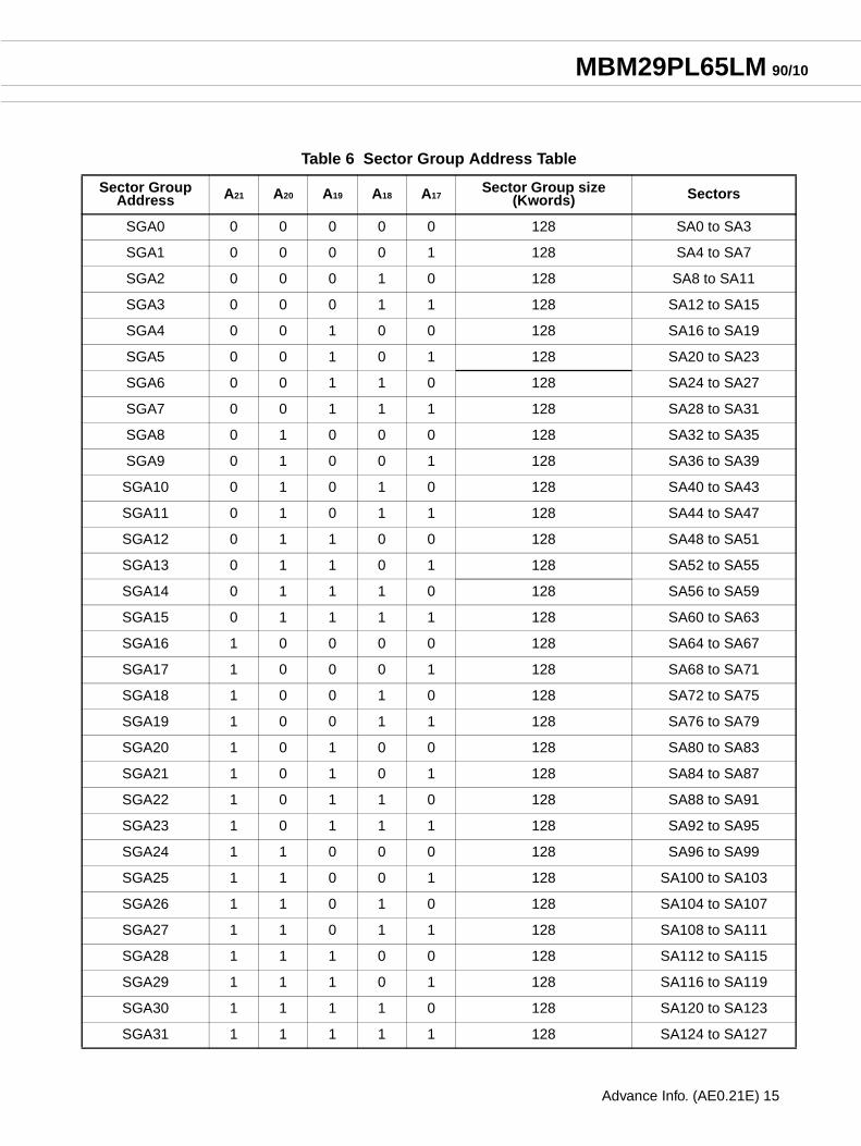
Table 6 Sector Group Address Table
Sector GroupAddress A21 A20 A19 A18 A17
Sector Group size(Kwords) Sectors
SGA0 0 0 0 0 0 128 SA0 to SA3
SGA1 0 0 0 0 1 128 SA4 to SA7
SGA2 0 0 0 1 0 128 SA8 to SA11
SGA3 0 0 0 1 1 128 SA12 to SA15
SGA4 0 0 1 0 0 128 SA16 to SA19
SGA5 0 0 1 0 1 128 SA20 to SA23
SGA6 0 0 1 1 0 128 SA24 to SA27
SGA7 0 0 1 1 1 128 SA28 to SA31
SGA8 0 1 0 0 0 128 SA32 to SA35
SGA9 0 1 0 0 1 128 SA36 to SA39
SGA10 0 1 0 1 0 128 SA40 to SA43
SGA11 0 1 0 1 1 128 SA44 to SA47
SGA12 0 1 1 0 0 128 SA48 to SA51
SGA13 0 1 1 0 1 128 SA52 to SA55
SGA14 0 1 1 1 0 128 SA56 to SA59
SGA15 0 1 1 1 1 128 SA60 to SA63
SGA16 1 0 0 0 0 128 SA64 to SA67
SGA17 1 0 0 0 1 128 SA68 to SA71
SGA18 1 0 0 1 0 128 SA72 to SA75
SGA19 1 0 0 1 1 128 SA76 to SA79
SGA20 1 0 1 0 0 128 SA80 to SA83
SGA21 1 0 1 0 1 128 SA84 to SA87
SGA22 1 0 1 1 0 128 SA88 to SA91
SGA23 1 0 1 1 1 128 SA92 to SA95
SGA24 1 1 0 0 0 128 SA96 to SA99
SGA25 1 1 0 0 1 128 SA100 to SA103
SGA26 1 1 0 1 0 128 SA104 to SA107
SGA27 1 1 0 1 1 128 SA108 to SA111
SGA28 1 1 1 0 0 128 SA112 to SA115
SGA29 1 1 1 0 1 128 SA116 to SA119
SGA30 1 1 1 1 0 128 SA120 to SA123
SGA31 1 1 1 1 1 128 SA124 to SA127
Advance Info. (AE0.21E) 15
16
MBM29PL65LM 90/10
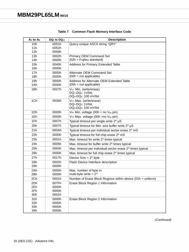
Table 7 Common Flash Memory Interface Code
(Continued)
A0 to A 6 DQ0 to DQ 15 Description10h11h12h
0051h0052h0059h
Query-unique ASCII string “QRY”
13h14h
0002h0000h
Primary OEM Command Set (02h = Fujitsu standard)
15h16h
0040h0000h
Address for Primary Extended Table
17h18h
0000h0000h
Alternate OEM Command Set(00h = not applicable)
19h1Ah
0000h0000h
Address for Alternate OEM Extended Table(00h = not applicable)
1Bh 0027h VCC Min. (write/erase)DQ7-DQ4: 1V/bit, DQ3-DQ0: 100 mV/bit
1Ch 0036h VCC Max. (write/erase)DQ7-DQ4: 1V/bit, DQ3-DQ0: 100 mV/bit
1Dh 0000h VPP Min. voltage (00h = no Vpp pin)1Eh 0000h VPP Max. voltage (00h =no Vpp pin)1Fh 0007h Typical timeout per single write 2N µS20h 0007h Typical timeout for Min. size buffer write 2N µS21h 000Ah Typical timeout per individual sector erase 2N mS22h 0000h Typical timeout for full chip erase 2N mS23h 0001h Max. timeout for write 2N times typical24h 0005h Max. timeout for buffer write 2N times typical25h 0004h Max. timeout per individual sector erase 2N times typical26h 0000h Max. timeout for full chip erase 2N times typical27h 0017h Device Size = 2N byte28h29h
0002h0000h
Flash Device Interface description
2Ah2Bh
0005h0000h
Max. number of byte in multi-byte write = 2N
2Ch 0001h Number of Erase Block Regions within device (01h = uniform)2Dh2Eh2Fh30h
007Fh0000h0000h0001h
Erase Block Region 1 Information
31h32h33h34h
0000h0000h0000h0000h
Erase Block Region 2 Information
(AE0.21E) Advance Info.

MBM29PL65LM 90/10
(Continued)A0 to A 6 DQ0 to DQ15 Description
35h36h37h38h
0000h0000h0000h0000h
Erase Block Region 3 Information
39h3Ah3Bh3Ch
0000h0000h0000h0000h
Erase Block Region 4 Information
40h41h42h
0050h0052h0049h
Query-unique ASCII string “PRI”
43h 0031h Major version number, ASCII44h 0033h Minor version number, ASCII45h 0008h Address Sensitive Unlock
Required46h 0002h Erase Suspend
(02h= To Read & Write)47h 0004h Number of sectors in per group48h 0001h Sector Temporary Unprotection
(01h = Supported)49h 0004h Sector Protection Algorithm4Ah 0000h Dual Operation
(00h = Not Supported)4Bh 0000h Burst Mode Type
(00h = Not Supported)4Ch 0001h Page Mode Type
(01h = 4-Word Page Supported)4Dh 00B5h VACC (Acceleration) Supply Minimum
DQ7-DQ4: 1V/bit, DQ3-DQ0: 100mV/bit
4Eh 00C5h VACC (Acceleration) Supply MaximumDQ7-DQ4: 1V/bit, DQ3-DQ0: 100mV/bit
4Fh 0004h Write Protect(04h = Uniform sectors bottom Write Protect)
50h 01h Program Suspend(01h = Supported)
Advance Info. (AE0.21E) 17

18
MBM29PL65LM 90/10
nnnn FUNCTIONAL DESCRIPTION
Standby Mode
There are two ways to implement the standby mode on the device, one using both the CE and RESET pins,and the other via the RESET pin only.
When using both pins, CMOS standby mode is achieved with CE and RESET input held at VCC ±0.3 V. Underthis condition the current consumed is less than 5 µA Max. During Embedded Algorithm operation, VCC activecurrent (ICC2) is required even when CE = "H”. The device can be read with standard access time (tCE) fromeither of these standby modes.
When using the RESET pin only, CMOS standby mode is achieved with RESET input held at VSS ±0.3 V (CE= “H” or “L”) . Under this condition the current consumed is less than 5 µA Max. Once the RESET pin is sethigh, the device requires tRH as a wake-up time for output to be valid for read access.
During standby mode, the output is in the high impedance state, regardless of OE input.
Automatic Sleep Mode
Automatic sleep mode works to restrain power consumption during read-out of device data. It can be useful in applications such as handy terminal, which requires low power consumption.
To activate this mode, the device automatically switch themselves to low power mode when the device addresses remain stable after tACC + 30 ns from data valid. It is not necessary to control CE, WE, and OE in this mode. The current consumed is typically 1 µA (CMOS Level).
Since the data are latched during this mode, the data are continuously read out. When the addresses are changed, the mode is automatically canceled and the device read-out the data for changed addresses.
Autoselect
The Autoselect mode allows reading out of a binary code and identifies its manufacturer and type.It is intendedfor use by programming equipment for the purpose of automatically matching the device to be programmedwith its corresponding programming algorithm.
To activate this mode, the programming equipment must force VID on address pin A9. Two identifier bytes may then be sequenced from the devices outputs by toggling A0. All addresses can be either High or Low except A6, A3,A2,A1 and A0. See Table 2.
The manufacturer and device codes may also be read via the command register, for instances when the device is erased or programmed in a system without access to high voltage on the A9 pin. The command sequence is illustrated in Table 3.Refer to Autoselect Command section.
In Word mode, a read cycle from address 00h returns the manufacturer’s code (Fujitsu = 04h) . A read cycleat address 01h outputs device code. When 227Eh is output, it indicates that two additional codes, calledExtended Device Codes will be required. Therefore the system may continue reading out these ExtendedDevice Codes at addresses of 0Eh and 0Fh. Refer to Table 4.
Read Mode
The device has two control functions required to obtain data at the outputs. CE is the power control andused for a device selection. OE is the output control and used to gate data to the output pins.
Address access time (tACC) is equal to the delay from stable addresses to valid output data. The chip enable access time (tCE) is the delay from stable addresses and stable CE to valid data at the output pins. The output enable access time is the delay from the falling edge of OE to valid data at the output pins. (Assuming the addresses have been stable for at least tACC-tOE time.) When reading out a data without changing addresses after power-up, input hardware reset or to change CE pin from “H” or “L”.
(AE0.21E) Advance Info.

MBM29PL65LM 90/10
Page Mode Read
The device is capable of fast read access for random locations within limited address location called Page. The Page size of the device is 4 words, within the appropriate Page being selected by the higher address bits A21 to A2 and the address bits A1 to A0 determining the specific word within that page. this is an asynchronous operation with the microprocessor supplying the specific word location.
The initial page access is equal to the random access (tACC) and subsequent Page read access (as long as the locations specified by the microprocessor fall within that Page) is equivalent to the page address access time(tPACC). Here again, CE selects the device and OE is the output control and should be used to gate data to the output pins if the device is selected. Fast Page mode, accesses are obtained by keeping A21 to A2 constant and changing A1 and A0 to select the specific word within that Page.
Output Disable
With the OE input at logic high level (VIH), output from the devices are disabled. This may cause the output pins to be in a high impedance state.
Write
Device erasure and programming are accomplished via the command register. The contents of the register serve as inputs to the internal state machine. The state machine outputs dictate the device function.
The command register itself does not occupy any addressable memory location. The register is a latch used to store the commands, along with the address and data information needed to execute the command. The command register is written by bringing WE to VIL, while CE is at VIL and OE is at VIH. Addresses are latched on the falling edge of WE or CE, whichever starts later; while data is latched on the rising edge of WE or CE, whichever starts first. Standard microprocessor write timings are used.
Refer to AC Write Characteristics and the Erase/Programming Waveforms for specific timing parameters.
Sector Group Protection
The device features hardware sector group protection. This feature will disable both program and eraseoperations in any combination of thirty two sector groups of memory.See Table 6. The user‘s side can usethe sector group protection using programming equipment. The device is shipped with all sector groups thatare unprotected.
To activate it, the programming equipment must force VID on address pin A9 and control pin OE, CE = VIL and A6 = A3 = A2 = A0 = VIL, A1 = VIH. The sector group addresses (A21, A20, A19, A18, A17, A16, and A15) should be set to the sector to be protected. Table 5 defines the sector address for each of the one hundred twenty-eight (128) individual sectors, and Table 6 defines the sector group address for each of the thirty-two (32) individual group sectors. Programming of the protection circuitry begins on the falling edge of the WE pulse and is terminated with the rising edge of the same. Sector group addresses must be held constant during the WE pulse. See Figures 17 and 25 for sector group protection timing diagram and algorithm.
To verify programming of the protection circuitry, the programming equipment must force VID on address pin A9 with CE and OE at VIL and WE at VIH. Scanning the sector group addresses (A21, A20, A19, A18, A17, A16, and A15) while (A6, A3, A2, A1, A0) = (0, 0, 0, 1, 0) will produce a logical “1” code at device output DQ0 for a protected sector. Otherwise the device will produce “0” for unprotected sectors. In this mode, the lower order addresses, except for A0, A1, A2, A3, and A6 can be either High or Low. Address locations with A1 = VIL are reserved for Autoselect manufacturer and device codes.
It is also possible to determine if a sector group is protected in the system by writing an Autoselect command. Performing a read operation at the address location XX02h, where the higher order addresses (A21, A20, A19, A18, A17, A16, and A15) are the desired sector group address will produce a logical “1” at DQ0 for a protected sector group. See Table 4 for Autoselect codes.
Advance Info. (AE0.21E) 19
20
MBM29PL65LM 90/10
Temporary Sector Group Unprotection
This feature allows temporary unprotection of previously protected sector groups of the devices in order to change data. The Sector Group Unprotection mode is activated by setting the RESET pin to high voltage (VID). During this mode, formerly protected sector groups can be programmed or erased by selecting the sector group addresses. Once the VID is taken away from the RESET pin, all the previously protected sector groups will be protected again. Refer to Figures 18 and 26.
Hardware Reset
The devices may be reset by driving the RESET pin to VIL from VIH. The RESET pin has a pulse requirementand has to be kept low (VIL) for at least “tRP” in order to properly reset the internal state machine. Any operationin the process of being executed will be terminated and the internal state machine will be reset to the readmode “tREADY” after the RESET pin is driven low. Furthermore, once the RESET pin goes high, the devicesrequire an additional “tRH” before it will allow read access. When the RESET pin is low, the devices will be inthe standby mode for the duration of the pulse and all the data output pins will be tri-stated. If a hardwarereset occurs during a program or erase operation, the data at that particular location will be corrupted.
Write Protect (WP )
The Write Protection function provides a hardware method of protecting certain first 32K words sector without using VID.
If the system asserts VIL on the WP pin, the device disables program and erase functions in the first 32K words sector independently of whether this sector was protected or unprotected using the method described in “Sector Group Protection" above.
If the system asserts VIH on the WP pin, the device reverts of whether the first 32K words sector was last set to be protected to the unprotected status. Sector protection or unprotection for this sector depends on whether this was last protected or unprotected using the method described in “Sector protection/unprotection”.
Accelerated Program Operation
The device offers accelerated program operation which enables programming in high speed. If the system asserts VACC to the ACC pin, the device automatically enters the acceleration mode and the time required for program operation will reduce to about 60%. This function is primarily intended to allow high speed programing, so caution is needed as the sector group becomes temporarily unprotected.
The system would use a fast program command sequence when programming during acceleration mode. Set command to fast mode and reset command from fast mode are not necessary. When the device enters the acceleration mode, the device is automatically set to fast mode. Therefore, the present sequence could be used for programming and detection of completion during acceleration mode.
Removing VACC from the ACC pin returns the device to normal operation. Do not remove VACC from the ACC pin while programming. See Figure 20.
Enhanced V CCQ Feature
The output voltage generated on the device is determined based on the VCCQ level. This feature allows the device to operate in mixed-voltage enviroments, driving and receiving signals to and from other devices on the same bus.
(AE0.21E) Advance Info.

MBM29PL65LM 90/10
nnnn COMMAND DEFINITIONS
Device operations are selected by writing specific address and data sequences into the command register. Table 3 shows the valid register command sequences. Note that the Erase Suspend (B0h) and Erase Resume (30h) commands are valid only while the Sector Erase operation is in progress. Also the Program Suspend (B0h) and Program Resume (30h) commands are valid only while the Program operation is in progress.Moreover Reset commands are functionally equivalent, resetting the device to the read mode. Please note that commands must be asserted to DQ7 to DQ0 and DQ15 to DQ8 bits are ignored.
Reset Command
In order to return from Autoselect mode or Exceeded Timing Limits (DQ5 = 1) to Read mode, the Reset operation is initiated by writing the Reset command sequence into the command register. The devices remain enabled for reads until the command register contents are altered.
The devices will automatically be in the reset state after power-up. In this case, a command sequence is not required in order to read data.
Autoselect Command
Flash memories are intended for use in applications where the local CPU alters memory contents. Therefore, manufacture and device codes must be accessible while the devices reside in the target system. PROM programmers typically access the signature codes by raising A9 to a high voltage. However applying high voltage onto the address lines is not generally desired system design practice.
The device contains an Autoselect command operation to supplement traditional PROM programming methodology. The operation is initiated by writing the Autoselect command sequence into the command register.
The Autoselect command sequence is initiated first by writing two unlock cycles. This is followed by a third write cycle that contains the address and the Autoselect command. Then the manufacture and device codes can be read from the address, and an actual data of memory cell can be read from the another address.
Following the command write, a read cycle from address 00h returns the manufactures’s code (Fujitsu =04h). A read cycle at address 01h outputs device code. When 227Eh is output, it indicates that two additionalcodes, called Extended Device Codes will be required. Therefore the system may continue reading out theseExtended Device Codes at address of 0Eh as well as at 0Fh. Refer to Table 4.
To terminate the operation, it is necessary to write the Reset command into the register. To execute the Autoselect command during the operation, Reset command must be written before the Autoselect command.
Advance Info. (AE0.21E) 21

22
MBM29PL65LM 90/10
Programming
The devices are programmed on a word-by-word basis. Programming is a four bus cycle operation. There are two “unlock” write cycles. These are followed by the program set-up command and data write cycles. Addresses are latched on the falling edge of CE or WE, whichever happens later and the data is latched on the rising edge of CE or WE, whichever happens first. The rising edge of CE or WE (whichever happens first) starts programming. Upon executing the Embedded Program Algorithm command sequence, the system is not required to provide further controls or timings. The device will automatically provide adequate internally generated program pulses and verify the programmed cell margin.
The system can determine the status of the program operation by using DQ7 (Data Polling), and DQ6 (Toggle Bit). The Data Polling and Toggle Bit are automatically performed at the memory location being programmed.
The programming operation is completed when the data on DQ7 is equivalent to data written to this bit at which the devices return to the read mode and plogram addresses are no longer latched. Therefore, the devices require that a valid address to the devices be supplied by the system at this particular instance. Hence Data Polling requires the same address which is being programmed.
If hardware reset occurs during the programming operation, the data being written is not guaranteed.
Programming is allowed in any address sequence and across sector boundaries. Beware that a data “0” cannot be programmed back to a “1”. Attempting to do so may result in either failure condition or an apparent success according to the data polling algorithm. But a read from Reset mode will show that the data is still “0”. Only erase operations can convert “0”s to “1”s.
Note that attempting to program a “1” over a “0” will result in programming failure. This precaution is the same with Fujitsu standard NOR devices. Figure 21 illustrates the Embedded ProgramTM Algorithm using typical command strings and bus operations.
Program Suspend/Resume
The Program Suspend command allows the system to interrupt a program operation so that data can be read from any address. Writing the Program Suspend command (B0h) during Embedded Program operation immediately suspends the programming. The Program Suspend command can also be issued during a programming operation while an erase is suspended. Refer to "Erase Suspend/Resume" for the detail.
When the Program Suspend command is written during a programming process, the device halts the program operation within 1us and updates the status bits.After the program operation has been suspended, the system can read data from any address. The data at program-suspended address is not valid. Normal read timing and command definitions apply.
After the Program Resume command (30h) is written, the device reverts to programming. The system can determine the status of the program operation using the DQ7 or DQ6 status bits, just as in the standard program operation. See "Write Operation Status" for more information.
The system also writes the Autoselect command sequence in the Program Suspend mode. The device allows reading Autoselect codes at the addresses within programming sectors, since the codes are not stored in the memory. When the device exits the Autoselect mode, the device reverts to the Program Suspend mode, and is ready for another valid operation. See "Autoselect Command Sequence" for more information.
The system must write the Program Resume command to exit from the Program Suspend mode and continue the programming operation. Further writes of the Resume command are ignored. Another Program Suspend command can be written after the device resumes programming.
(AE0.21E) Advance Info.
MBM29PL65LM 90/10
Write Buffer Programming Operations
Write Buffer Programming allows the system write to series of 16 words in one programming operation. This results in faster effective word programming time than the standard programming algorithms. The Write Buffer Programming command sequence is initiated by first writing two unlock cycles. This is followed by a third write cycle selecting the Sector Address in which programming will occur. In forth cycle contains both Sector Address and unique code for data bus width will be loaded into the page buffer at the Sector Address in which programming will occur.
The system then writes the starting address/data combination. This “starting address” must be the same Sector Address used in third and fourth cycles and its lower addresses of A3 to A0 should be 0h. All subsequent address must be incremented by 1. Addresses are latched on the falling edge of CE or WE, whichever happens later and the data is latched on the rising edge of CE or WE, whichever happens first. The rising edge of CE or WE (whichever happens first) starts programming. Upon executing the Write Buffer Programming Operations command sequence, the system is not required to provide further controls or timings. The device will automatically provide adequate internally generated program pulses and verify the programmed cell margin.
DQ7(Data Polling), DQ6(Toggle Bit), DQ5(Exceeded Timing Limits), DQ1(Write-to-Buffer Abort) should be monitored to determine the device status during Write Buffer Programming. In addition to these functions, it is also possible to indicate to the host system that Write Buffer Programming Operations are either in progress or have been completed by RY/BY. See Table 9 "Hardware Sequence Flags".
The Data polling techniques described in Figure 23 should be used while monitoring the last address location loaded into the write buffer. In addition, it is not neccessary to specify an address in Toggle Bit techniques described in Figure 24. The automatic programing operation is completed when the data on DQ7 is equivalent to the data written to this bit at which time the device returns to the read mode and addresses are no longer latched ( See Table 9 " Hardware Sequence Flags").
The write-buffer programming operation can be suspended using the standard program suspend/resume commands.
Once the write buffer programming is set, the system must then write the “Program Buffer to Flash” command at the Sector Address. Any other address/data combination will abort the Write Buffer Programming operation and the device will continue busy state.
The Write Buffer Programming Sequence can be ABORTED by doing the following : • Different Sector Address is asserted.• Write data other than the “Program Buffer to Flash" command after the specified number of “data load”
cycles.
A “Write-to-Buffer-Abort Reset” command sequence must be written to the device to return to read mode. (See Table 3 for details on this command sequence.)
Advance Info. (AE0.21E) 23
24
MBM29PL65LM 90/10
Chip Erase
Chip erase is a six bus cycle operation. It begins two “unlock” write cycles followed by writing the “set-up” command, and two “unlock” write cycles followed by the chip erase command which invokes the Embedded Erase algorithm.
The device does not require the user to program the device prior to erase. Upon executing the Embedded Erase Algorithm the device automatically programs and verifies the entire memory for an all zero data pattern prior to electrical erase (Preprogram function). The system is not required to provide any controls or timings during these operations.
The system can determine the status of the erase operation by using DQ7 (Data Polling), DQ6 (Toggle Bit I) and DQ2 (Toggle Bit II). The chip erase begins on the rising edge of the last CE or WE, whichever happens first from last command sequence and completes when the data on DQ7 is “1” (See Write Operation Status section.) at which time the device returns to read mode.
Sector Erase
Sector erase is a six bus cycle operation. There are two “unlock” write cycles. These are followed by writing the “set-up” command. Two more “unlock” write cycles are then followed by the Sector Erase command.
Multiple sectors may be erased concurrently by writing the same six bus cycle operations. This sequence is followed by writes of the Sector Erase command to addresses in other sectors desired to be concurrently erased. The time between writes must be less than Erase Time-out time(tTOW). Otherwise that command will not be accepted and erasure will not start. It is recommended that processor interrupts be disabled during this time to guarantee this condition. The interrupts can reoccur after the last Sector Erase command is written. A time-out of “tTOW” from the rising edge of last CE or WE, whichever happens first, will initiate the execution of the Sector Erase command(s). If another falling edge of CE or WE, whichever happens first occurs within the “tTOW” time-out window the timer is reset (monitor DQ3 to determine if the sector erase timer window is still open, see section DQ3, Sector Erase Timer). Resetting the devices once execution has begun will corrupt the data in the sector. In that case, restart the erase on those sectors and allow them to complete (refer to the Write Operation Status). Loading the sector erase buffer may be done in any sequence and with any number of sectors (0 to 127).
Sector erase does not require the user to program the devices prior to erase. The devices automatically program all memory locations in the sector(s) to be erased prior to electrical erase using the Embedded Erase Algorithm. When erasing a sector, the remaining unselected sectors remain unaffected. The system is not required to provide any controls or timings during these operations.
The system can determine the status of the erase operation by using DQ7 (Data Polling), DQ6 (Toggle Bit I), and DQ2 (Toggle Bit II).
The sector erase begins after the “tTOW” time-out from the rising edge of CE or WE whichever happens first for the last sector erase command pulse and completes when the data on DQ7 is “1” (see Write Operation Status section), at which the devices return to the read mode. Data polling and Toggle Bit must be performed at an address within any of the sectors being erased.
(AE0.21E) Advance Info.

MBM29PL65LM 90/10
Erase Suspend/Resume
The Erase Suspend command allows the user to interrupt Sector Erase operation and then perform read or programming to a sector not being erased. This command is applicable ONLY during the Sector Erase operation within the time-out period for sector erase. Writting the Erase Suspend command (B0h) during the Sector Erase time-out results in immediate termination of the time-out period and suspension of the erase operation.
Writing the "Erase Resume" command (30h) resumes the erase operation.
When the "Erase Suspend" command is written during the Sector Erase operation, the device takes maximum of “tSPD” to suspend the erase operation. When the devices enter the erase-suspended mode, the RY/BY output pin will be at Hi-Z and the DQ7 bit will be at logic “1” and DQ6 will stop toggling. The user must use the address of the erasing sector for reading DQ6 and DQ7 to determine if the erase operation has been suspended. Further writes of the Erase Suspend command are ignored.
When the erase operation is suspended, the devices default to the erase-suspend-read mode. Reading data in this mode is the same as reading from the standard read mode, except that the data must be read from sectors that have not been erase-suspended. Reading successively from the erase-suspended sector while the device is in the erase-suspend-read mode will cause DQ2 to toggle. see the section on DQ2.
After entering the erase-suspend-read mode, the user can program the device by writing the appropriate command sequence for Program. This program mode is known as the erase-suspend-program mode. Again, it is the same as programming in the regular Program mode, except that the data must be programmed to sectors that are not erase-suspended. Reading successively from the erase-suspended sector while the devices are in the erase-suspend-program mode will cause DQ2 to toggle. The end of the erase-suspended Program operation is detected by the Data polling of DQ7 or by the Toggle Bit I of DQ6, which is the same as the regular Program operation. Note that DQ7 must be read from the Program address while DQ6 can be read from any address.
To resume the operation of Sector Erase, the Resume command (30h) should be written. Any further writes of the Resume command at this point will be ignored. Another Erase Suspend command can be written after the chip has resumed erasing.
Fast Mode Set/Reset
The device has Fast Mode function. It dispenses with the initial two unclock cycles required in the standard program command sequence by writing Fast Mode command into the command register. In this mode, the required bus cycle for programming consists of two cycles instead of four bus cycles in standard program command. Do not write erase command in this mode. The read operation is also executed after exiting this mode. To exit from this mode, write Fast Mode Reset command into the command register. (Refer to the Figure 28.) The VCC active current is required even CE = VIH during Fast Mode.
Fast Programming
During Fast Mode, the programming can be executed with two bus cycles operation. The Embedded Program Algorithm is executed by writing program set-up command (A0h) and data write cycles (PA/PD). see Figure 28.
Extended Sector Group Protection
In addition to normal sector group protection, the device has Extended Sector Group Protection as extended function. This function enables protection of the sector group by forcing VID on RESET pin and writes a command sequence. Unlike conventional procedures, it is not necessary to force VID and control timing for control pins. The only RESET pin requires VID for sector group protection in this mode. The extended sector group protection requires VID on RESET pin. With this condition, the operation is initiated by writing the set-up command (60h) into the command register. Then the sector group addresses pins (A21, A20, A19, A18, A17,
A16 and A15) and (A6, A3, A2, A1, A0) = (0, 0, 0, 1, 0) should be set to the sector group to be protected (set VIL for the other addresses pins is recommended), and write extended sector group protection command (60h). A sector group is typically protected in 250 µs. To verify programming of the protection circuitry, the sector
Advance Info. (AE0.21E) 25

26
MBM29PL65LM 90/10
group addresses pins (A21, A20, A19, A18, A17, A16 and A15) and (A6, A3, A2, A1, A0) = (0, 0, 0, 1, 0) should be set and write a command (40h). Following the command write, a logical “1” at device output DQ0 will produce for protected sector in the read operation. If the output data is logical “0”, write the extended sector group protection command (60h) again. To terminate the operation, set RESET pin to VIH. (Refer to the Figures 19 and 27.)
Query Command (CFI : Common Flash Memory Interface)
The CFI (Common Flash Memory Interface) specification outlines device and host system software interrogation handshake which allows specific vendor-specified software algorithms to be used for entire families of devices. This allows device-independent, JEDEC ID-independent, and forward-and backward-compatible software support for the specified flash device families. Refer to CFI specification in detail.
The operation is initiated by writing the query command (98h) into the command register. Following the command write, a read cycle from specific address retrieves device information. Please note that output data of upper byte (DQ15 to DQ8) is “0”. Refer to the CFI code table. To terminate operation, it is necessary to write the Reset command sequence into the register. (See Table 7.)
HiddenROM (Hi-ROM) Mode
(1)HiddenROM (Hi-ROM) Region
The HiddenROM (Hi-ROM) feature provides a Flash memory region that the system may access through a new command sequence. This is primarily intended for customers who wish to use an Electronic Serial Number (ESN) in the device with the ESN protected against modification. Once the Hi-ROM region is protected, any further modification of that region is impossible. This ensures the security of the ESN once the product is shipped to the field.
The Hi-ROM region is 128 words in length. After the system writes the Hi-ROM Entry command sequence, it may read the Hi-ROM region by using device addresses A6 to A0 (A21 to A7 are all “0”). That is, the device sends only program command that would normally be sent to the address to the Hi-ROM region. This mode of operation continues until the system issues the Exit Hi-ROM command sequence, or until power is removed from the device. On power-up, or following a hardware reset, the device reverts to sending commands to the address.
If you request Fujitsu to program the ESN in the device, please contact a Fujitsu representative for more information.
(2) HiddenROM (Hi-ROM) Entry Command
The device has a Hi-ROM area with One Time Protect function. This area is to enter the security code andto unable the change of the code once set. Programming is allowed in this area until it is protected. However,once it gets protected, it is impossible to unprotect. Therefore, extreme caution is required.
The hidden ROM area is 128 words. This area is in SA0 . Therefore, write the Hi-ROM entry commandsequence to enter the Hi-ROM area. It is called Hi-ROM mode when the Hi-ROM area appears.
Sectors other than the block area SA0 can be read during Hi-ROM mode. Read/program of the Hi-ROMarea is possible during Hi-ROM mode. Write the Hi-ROM reset command sequence to exit the Hi-ROM mode.
(3) HiddenROM (Hi-ROM) Program Command
To program the data to the Hi-ROM area, write the Hi-ROM program command sequence during Hi-ROMmode. This command is the same as the usual program command, except that it needs to write the commandduring Hi-ROM mode. Therefore the detection of completion method is the same as in the past, using theDQ7 data pooling and DQ6 Toggle bit. You should pay attention to the address to be programmed. If anaddress not in the Hi-ROM area is selected, the previous data will be deleted.
(AE0.21E) Advance Info.

MBM29PL65LM 90/10
(4) HiddenROM (Hi-ROM) Protect Command
There are two methods to protect the Hi-ROM area. One is to write the sector group protect setup command(60h) , set the sector address in the Hi-ROM area and (A6, A3, A2, A1, A0) = (0, 0, 0, 1, 0) , and write thesector group protect command (60h) during the Hi-ROM mode. The same command sequence may be usedbecause it is the same as the extension sector group protect in the past, except that it is in the Hi-ROM modeand does not apply high voltage to the RESET pin. Please refer to above mentioned “Extended Sector GroupProtection” for details of sector group protect setting.The other method is to apply high voltage (VID) to A9 and OE, set the sector address in the Hi-ROM areaand (A6, A3, A2, A1, A0) = (0, 0, 0, 1, 0) , and apply the write pulse during the Hi-ROM mode. To verify theprotect circuit, apply high voltage (VID) to A9, specify (A6, A3, A2, A1, A0) = (0, 0, 0, 1, 0) and the sector addressin the Hi-ROM area, and read. When “1” appears on DQ0, the protect setting is completed. “0” will appearon DQ0 if it is not protected. Apply write pulse again. The same command sequence could be used for theabove method because other than the Hi-ROM mode, it is the same as the sector group protect previouslymentioned.
Take note that other sector groups will be affected if an address other than those for the Hi-ROM area isselected for the sector group address, so please be careful. Pay close attention that once it is protected,protection CANNOT BE CANCELLED.
Advance Info. (AE0.21E) 27
28
MBM29PL65LM 90/10
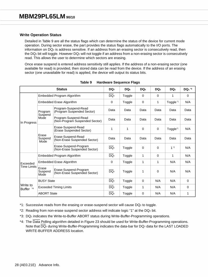
Write Operation Status
Detailed in Table 9 are all the status flags which can determine the status of the device for current mode operation. During sector erase, the part provides the status flags automatically to the I/O ports. The information on DQ2 is address sensitive. If an address from an erasing sector is consecutively read, then the DQ2 bit will toggle. However DQ2 will not toggle if an address from a non-erasing sector is consecutively read. This allows the user to determine which sectors are erasing.
Once erase suspend is entered address sensitivity still applies. If the address of a non-erasing sector (one available for read) is provided, then stored data can be read from the device. If the address of an erasing sector (one unavailable for read) is applied, the device will output its status bits.
*1: Successive reads from the erasing or erase-suspend sector will cause DQ2 to toggle.
*2: Reading from non-erase suspend sector address will indicate logic “1” at the DQ2 bit.
*3: DQ1 indicates the Write-to-Buffer ABORT status during Write-Buffer-Programming operations.
*4: The Data Polling algorithm detailed in Figure 23 should be used for Write-Buffer-Programming operations.Note that DQ7 during Write-Buffer-Programming indicates the data-bar for DQ7 data for the LAST LOADEDWRITE-BUFFER ADDRESS location.
Table 9 Hardware Sequence Flags
Status DQ7 DQ6 DQ5 DQ3 DQ2 DQ1 *3
In Progress
Embedded Program Algorithm DQ7 Toggle 0 0 1 0
Embedded Erase Algorithm 0 Toggle 0 1 Toggle *1 N/A
ProgramSuspendMode
Program-Suspend-Read(Program Suspended Sector) Data Data Data Data Data Data
Program-Suspend-Read(Non-Program Suspended Sector) Data Data Data Data Data Data
Erase Suspend Mode
Erase-Suspend-Read (Erase Suspended Sector) 1 1 0 0 Toggle*1 N/A
Erase-Suspend-Read (Non-Erase Suspended Sector) Data Data Data Data Data Data
Erase-Suspend-Program (Non-Erase Suspended Sector) DQ7 Toggle 0 0 1 *2 N/A
ExceededTime Limits
Embedded Program Algorithm DQ7 Toggle 1 0 1 N/A
Embedded Erase Algorithm 0 Toggle 1 1 N/A N/A
Erase Suspend Mode
Erase-Suspend-Program (Non-Erase Suspended Sector) DQ7 Toggle 1 0 N/A N/A
Write to Buffer *4
BUSY State DQ7 Toggle 0 N/A N/A 0
Exceeded Timing Limits DQ7 Toggle 1 N/A N/A 0
ABORT State DQ7 Toggle 0 N/A N/A 1
(AE0.21E) Advance Info.

MBM29PL65LM 90/10
DQ7
Data Polling
The devices feature Data Polling as a method to indicate to the host that the Embedded Algorithms are in progress or completed. During the Embedded Program Algorithm, an attempt to read devices will produce reverse data last written to DQ7. Upon completion of the Embedded Program Algorithm, an attempt to read the device will produce true data last written to DQ7. During the Embedded Erase Algorithm, an attempt to read the device will produce a “0” at the DQ7 output. Upon completion of the Embedded Erase Algorithm, an attempt to read device will produce a “1” at the DQ7 output. The flowchart for Data Polling (DQ7) is shown in Figure 23.
For programming, the Data Polling is valid after the rising edge of fourth write pulse in the four write pulse sequence.
For chip erase and sector erase, the Data Polling is valid after the rising edge of the sixth write pulse in the six write pulse sequence. Data Polling must be performed at sector addresses of sectors being erased, not protected sectors. Otherwise, the status may become invalid.
If a program address falls within a protected sector, Data polling on DQ7 is active for approximately 1 µs, then the device returns to read mode. After an erase command sequence is written, if all sectors selected for erasing are protected, Data Polling on DQ7 is active for approximately 400 µs, then the device returns to read mode. If not all selected sectors are protected, the Embedded Erase algorithm erases the unprotected sectors, and ignores the selected sectors that are protected.
Once the Embedded Algorithm operation is close to being completed, the device data pins (DQ7) may change asynchronously while the output enable (OE) is asserted low. This means that the device is driving status information on DQ7 at one instant of time, and then that byte’s valid data the next. Depending on when the system samples the DQ7 output, it may read the status or valid data. Even if the device completes the Embedded Algorithm operation and DQ7 has a valid data, the data outputs on DQ6 to DQ0 may still be invalid. The valid data on DQ7 to DQ0 will be read on the successive read attempts.
The Data Polling feature is active only during the Embedded Programming Algorithm, Embedded Erase Algorithm, Erace Suspendmode or sector erase time-out.
See Figure 12 for the Data Polling timing specifications and diagram.
DQ6
Toggle Bit I
The device also feature the “Toggle Bit I” as a method to indicate to the host system that the Embedded Algorithms are in progress or completed.
During an Embedded Program or Erase Algorithm cycle, successive attempts to read (CE or OE toggling) data from the devices will result in DQ6 toggling between one and zero. Once the Embedded Program or Erase Algorithm cycle is completed, DQ6 will stop toggling and valid data will be read on the next successive attempts. During programming, the Toggle Bit I is valid after the rising edge of the fourth write pulse in the four write pulse sequences. For chip erase and sector erase, the Toggle Bit I is valid after the rising edge of the sixth write pulse in the six write pulse sequences. The Toggle Bit I is active during the sector time out.
In programm operation, if the sector being written to is protected, the Toggle bit will toggle for about 1 µs and then stop toggling with the data unchanged. In erase, the device will erase all the selected sectors except for the protected ones. If all selected sectors are protected, the chip will toggle the Toggle bit for about 400 µs and then drop back into read mode, having data kept remained.
Either CE or OE toggling will cause the DQ6 to toggle. See Figure 13 for the Toggle Bit I timing specifications and diagram.
DQ5
Exceeded Timing Limits
Advance Info. (AE0.21E) 29
30
MBM29PL65LM 90/10
DQ5 will indicate if the program or erase time has exceeded the specified limits (internal pulse count). Under these conditions DQ5 will produce a “1”. This is a failure condition indicating that the program or erase cycle was not successfully completed. Data Polling is the only operating function of the device under this condition. The CE circuit will partially power down the device under these conditions (to approximately 2 mA). The OE and WE pins will control the output disable functions as described in Table 2.
The DQ5 failure condition may also appear if a user tries to program a non blank location without pre-erase. In this case the device locks out and never completes the Embedded Algorithm operation. Hence, the system never reads a valid data on DQ7 bit and DQ6 never stop toggling. Once the device has exceeded timing limits, the DQ5 bit will indicate a “1”. Note that this is not a device failure condition since the device was incorrectly used. If this occurs, reset the device with command sequence.
DQ3
Sector Erase Timer
After the completion of the initial sector erase command sequence the sector erase time-out will begin. DQ3 will remain low until the time-out is complete. Data Polling and Toggle Bit are valid after the initial sector erase command sequence.
If Data Polling or the Toggle Bit I indicates a valid erase command has been written, DQ3 may be used to determine whether the sector erase timer window is still open. If DQ3 is “1” the internally controlled erase cycle has begun. If DQ3 is “0”, the device will accept additional sector erase commands. To insure the command has been accepted, the system software should check the status of DQ3 prior to and following each subsequent Sector Erase command. If DQ3 were high on the second status check, the command may not have been accepted.
See Table 9, Hardware Sequence Flags.
DQ2
Toggle Bit II
This Toggle Bit II, along with DQ6, can be used to determine whether the devices are in the Embedded Erase Algorithm or in Erase Suspend.
Successive reads from the erasing sector will cause DQ2 to toggle during the Embedded Erase Algorithm. If the devices are in the erase-suspended-read mode, successive reads from the erase-suspended sector will cause DQ2 to toggle. When the device is in the erase-suspended-program mode, successive reads from the non-erase suspended sector will indicate a logic “1” at the DQ2 bit.
DQ6 is different from DQ2 in that DQ6 toggles only when the standard program or Erase, or Erase Suspend Program operation is in progress. The behavior of these two status bits, along with that of DQ7, is summarized as follows:
For example, DQ2 and DQ6 can be used together to determine if the erase-suspend-read mode is in progress. (DQ2 toggles while DQ6 does not.) See also Table 9 and Figure 14.
Furthermore, DQ2 can also be used to determine which sector is being erased. At the erase mode, DQ2 toggles if this bit is read from an erasing sector.
Reading Toggle Bits DQ 6 / DQ2
Whenever the system initially begins reading Toggle bit status, it must read DQ7 to DQ0 at least twice in arow to determine whether a Toggle bit is toggling. Typically a system would note and store the value of theToggle bit after the first read. After the second read, the system would compare the new value of the Togglebit with the first. If the Toggle bit is not toggling, the device has completed the program or erase operation.The system can read array data on DQ7 to DQ0 on the following read cycle.
However, if, after the initial two read cycles, the system determines that the Toggle bit is still toggling, thesystem also should note whether the value of DQ5 is high (see the section on DQ5) . If it is, the system shouldthen determine again whether the Toggle bit is toggling, since the Toggle bit may have stopped toggling just
(AE0.21E) Advance Info.

MBM29PL65LM 90/10
as DQ5 went high. If the Toggle bit is no longer toggling, the device has successfully completed the programor erase operation. If it is still toggling, the device did not complete the operation successfully, and the systemmust write the reset command to return to reading array data.
The remaining scenario is that the system initially determines that the Toggle bit is toggling and DQ5 has notgone high. The system may continue to monitor the Toggle bit and DQ5 through successive read cycles,determining the status as described in the previous paragraph. Alternatively, it may choose to perform othersystem tasks. In this case, the system must start at the beginning of the algorithm when it returns to determinethe status of the operation. (Refer to Figure 24.)
Table 10 Toggle Bit Status
*1: : Successive reads from the erasing or erase-suspend sector will cause DQ2 to toggle.
*2: : Reading from the non-erase suspend sector address will indicate logic “1” at the DQ2 bit.
DQ1
Write-to-Buffer Abort
DQ1 indicates whether a Write-to-Buffer operation was aborted. Under these conditions DQ1 produces a "1" The system must issue the Write-to-Buffer-Abort-Reset command sequence to return the device to reading array data. See "Write Buffer Programming Operations" section for more details.
Data Protection
The device is designed to offer protection against accidental erasure or programming caused by spurious system level signals that may exist during power transitions. During power up the device automatically reset the internal state machine in Read mode. Also, with its control register architecture, alteration of memory contents only occurs after successful completion of specific multi-bus cycle command sequences.
The device also incorporates several features to prevent inadvertent write cycles resulting form VCC power-up and power-down transitions or system noise.
(1) Low V CC Write Inhibit
To avoid initiation of a write cycle during VCC power-up and power-down, a write cycle is locked out for VCC less than VLKO. If VCC < VLKO, the command register is disabled and all internal program/erase circuits are disabled. Under this condition, the device will reset to the read mode. Subsequent writes will be ignored until the VCC level is greater than VLKO. It is the user’s responsibility to ensure that the control pins are logically correct to prevent unintentional writes when VCC is above VLKO.
If Embedded Erase Algorithm is interrupted, the intervened erasing sector(s) is(are) not valid.
(2) Write Pulse “Glitch” Protection
Noise pulses of less than 3 ns (typical) on OE, CE, or WE will not initiate a write cycle.
(3) Logical Inhibit
Writing is inhibited by holding any one of OE = VIL, CE = VIH, or WE = VIH. To initiate a write, CE and WE must be a logical zero while OE is a logical one.
Mode DQ 7 DQ6 DQ2
Program DQ7 Toggle 1
Erase 0 Toggle Toggle *1
Erase-Suspend-Read (Erase-Suspended Sector)
1 1 Toggle *1
Erase-Suspend-Program DQ7 Toggle 1 *2
Advance Info. (AE0.21E) 31

32
MBM29PL65LM 90/10
(4) Power-up Write Inhibit
Power-up of the devices with WE = CE = VIL and OE = VIH will not accept commands on the rising edge of WE. The internal state machine is automatically reset to read mode on power-up.
(5) Sector Protection
Device user is able to protect each sector group individually to store and protect data. Protection circuit voids both program and erase commands that are addressed to protected sectors.Any commands to program or erase addressed to protected sector are ignored .
(AE0.21E) Advance Info.

MBM29PL65LM 90/10
nnnn ABSOLUTE MAXIMUM RATINGS
*1: Voltage is defined on the basis of VSS = GND = OV.
*2: Minimum DC voltage on input or I/O pins is –0.5 V. During voltage transitions, input or I/O pins may undershootVSS to –0.2 V for periods of up to 20 ns. Maximum DC voltage on input or I/O pins is VCC +0.5 V. Duringvoltage transitions, input or I/O pins may overshoot to VCC +2.0 V for periods of up to 20 ns
*3: Minimum DC input voltage is –0.5V. During voltage transitions, these pins may undershoot VSS to –0.2 Vfor periods of up to 20 ns.Voltage difference between input and supply voltage ( VIN–VCC) dose not exceedto +9.0 V. Maximum DC input voltage is +12.5 V which may overshoot to +14.0 V for periods of up to 20 ns.
WARNING: Semiconductor devices can be permanently damaged by application of stress (voltage, current, temperature, etc.) in excess of absolute maximum ratings. Do not exceed these ratings.
nnnn RECOMMENDED OPERATING RANGES Note *1
Notes: *1. Operating ranges define those limits between which the functionality of the device is guaranteed. *2. Voltage is defined on the basis of VSS = GND = 0V. *3. VCC and VCCQ supply voltage must be on the same level.
WARNING: The recommended operating conditions are required in order to ensure the normal operation of the semiconductor device. All of the device’s electrical characteristics are warranted when the device is operated within these ranges. Always use semiconductor devices within their recommended operating condition ranges. Operation outside these ranges may adversely affect reliability and could result in device failure.No warranty is made with respect to uses , operating conditions, or combinations not represented on the data sheet. Users considering application outside the listed conditions are advised to contact their FUJITSU representatives beforehand.
Parameter SymbolRating
UnitMin. Max.
Storage Temperature Tstg –55 +125 °C
Ambient Temperature with Power Applied TA –40 +85 °C
Voltage with Respect to Ground All Pins Except A9, OE, and RESET *1,*2
VIN, VOUT –0.5 VCC +0.5 V
Power Supply Voltage *1 VCC,VCCQ –0.5 +4.0 V
A9, OE, and RESET *1,*3 VIN –0.5 +12.5 V
ACC *1,*3 VACC –0.5 +12.5 V
Parameter SymbolValue
UnitMin. Max.
Ambient Temperature90
TA–20 +70
°C100 –40 +85
VCC Supply Voltage *2, *3 VCC +3.0 +3.6 V
VCCQ Supply Voltage *2, *3 VCCQ VCC V
Advance Info. (AE0.21E) 33
34
MBM29PL65LM 90/10
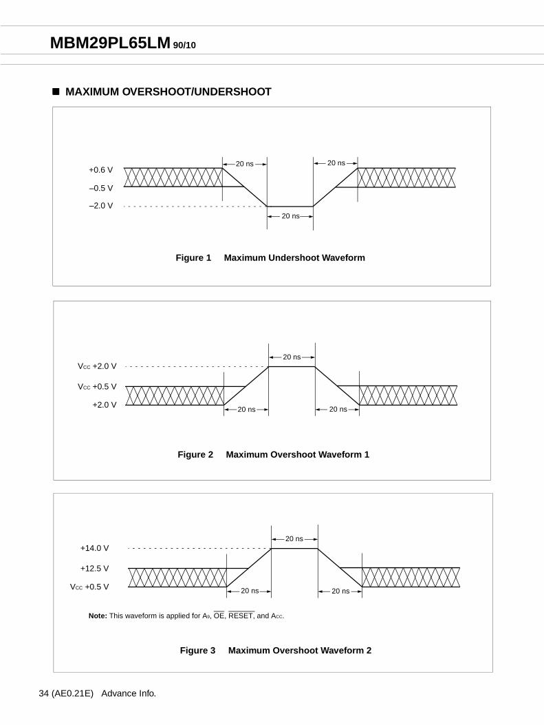
nnnn MAXIMUM OVERSHOOT/UNDERSHOOT
Figure 1 Maximum Undershoot Waveform
+0.6 V
–0.5 V
20 ns
–2.0 V20 ns
20 ns
Figure 2 Maximum Overshoot Waveform 1
+2.0 V
VCC +0.5 V
20 ns
VCC +2.0 V20 ns
20 ns
Figure 3 Maximum Overshoot Waveform 2
VCC +0.5 V
+12.5 V
20 ns
+14.0 V20 ns
20 ns
Note: This waveform is applied for A9, OE, RESET, and ACC.
(AE0.21E) Advance Info.

MBM29PL65LM 90/10
µA
µA
µA
A
A
A
A
µA
µA
µA
A
A
V
V
V
V
V
V
V
nnnn ELECTRICAL CHARACTERISTICS
1.DC Characteristics
Notes: *1. The lCC current listed includes both the DC operating current and the frequency dependent component.*2. Maximum ICC values are tested with VCC = VCC Max. and VCCQ = VCCQ Max.*3. lCC active while Embedded Erase or Embedded Program or Write Buffer Programming is in progress.*4. Automatic sleep mode enables the low power mode when address remain stable for tACC + 30 ns.
Parameter Description Symbol Conditions Min. Typ. Max. Unit
Input Leakage Current ILIVIN = VSS to VCC, VCC = VCC Max.
WP Pin –2.0 — +2.0
Others –1.0 — +1.0
Output Leakage Current ILO VOUT = VSS to VCC, VCC = VCC Max. –1.0 — +1.0
A9, OE, RESET Inputs Leakage Current ILIT
VCC = VCC Max.,A9, OE, RESET = 12.5 V — — 35
VCC Active Current (Read) *1,*2 ICC1
CE = VIL, OE = VIH, f = 5 MHz — 15 25 m
CE = VIL, OE = VIH, f = 10 MHz — 35 50 m
VCC Active Current (Intra-Page Read) *2 ICC2 CE = VIL, OE = VIH, tPRC = 25ns, 4-Word — 10 20 m
VCC Active Current (Program / Erase) *2,*3 ICC3 CE = VIL, OE = VIH — 50 60 m
VCC Standby Current *2 ICC4CE = VCC ±0.3 V, RESET = VCC ±0.3 V,OE = VIH, WP = VCC ±0.3 V — 1 5
VCC Reset Current *2 ICC5RESET = VCC ±0.3 V,WP = VCC ±0.3 V — 1 5
VCC Automatic Sleep Current *3,*4 ICC6
CE = VSS ±0.3 V, RESET = VCC ±0.3 V,VIN = VCC ±0.3V or Vss ±0.3V, WP = VCC ±0.3 V
— 1 5
VCC Active Current(Erase-Suspend-Program) *2 ICC7 CE = VIL, OE = VIH — 50 60 m
ACC Accelerated Program Current IACC
CE = VIL, OE = VIH,Vcc = Vcc Max.,ACC =VACC Max.
ACC Pin — — 45m
Vcc Pin — — 60
Input Low Level VIL — –0.5 — 0.6
Input High Level VIH — 0.7×VCC —VCC + 0.3
Voltage for ACC Sector Protection/Unprotection and Program Acceleration
VACC VCC = 2.7 V to 3.6 V 11.5 12.0 12.5
Voltage for Autoselect, andTemporary Sector Unprotected VID VCC = 2.7 V to 3.6 V 11.5 12.0 12.5
Output Low Voltage Level VOLIOL = 4.0 mA, VCC = VCC Min.,VCCQ = VCCQ Min. — — 0.45
Output High Voltage Level VOHIOH = –2.0 mA, VCC = VCC Min.,VCCQ = VCCQ Min. 0.85×VCCQ — —
Low VCC Lock-Out Voltage VLKO — 2.3 — 2.5
Advance Info. (AE0.21E) 35

36
MBM29PL65LM 90/10
2.AC Characteristics
• Read Only Operations Characteristics
Parameter SymbolsDescription Condition
Value*1
Unit90 10JEDEC Standard
tAVAV tRC Read Cycle Time — Min. 90 100 ns
tAVQV tACC Address to Output Delay CE = VIL,
OE = VILMax. 90 100 ns
tELQV tCE Chip Enable to Output Delay OE = VIL Max. 90 100 ns
— tPRC Page Read Cycle Time — Max. 25 30 ns
— tPACC Page Address to Output Delay CE = VIL,
OE = VILMax. 25 30 ns
tGLQV tOE Output Enable to Output Delay — Max. 25 30 ns
tEHQZ tDF Chip Enable to Output High-Z — Max. 25 30 ns
— tOEHOutput Enable Hold Time
Read — Min. 0 ns
Toggle and Data Polling — Min. 10 ns
tGHQZ tDF Output Enable to Output High-Z — Max. 25 30 ns
tAXQX tOHOutput Hold Time From Addresses, CE or OE, Whichever Occurs First — Min. 0 ns
— tREADY RESET Pin Low to Read Mode — Max. 20 µs
Note: *1. Test Conditions;Output Load: 1 TTL gate and 30 pFInput rise and fall times: 5 nsInput pulse levels: 0.0 V or VCC Timing measurement reference level
Input : VCC / 2Output : VCC / 2
Figure 4 Test Conditions
CL
3.3 V
Diodes = IN3064or Equivalent
2.7 kΩDeviceUnderTest
IN3064or Equivalent
6.2 kΩ
(AE0.21E) Advance Info.

MBM29PL65LM 90/10
• Write (Erase/Program) Operations
(Continued)
Parameter SymbolsParameter
ValueUnit
90 10JEDEC Standard
tAVAV tWC Write Cycle Time Min. 90 100 ns
tAVWL tAS Address Setup Time Min. 0 ns
— tASOAddress Setup Time to OE Low During Toggle Bit Polling Min. 15 ns
tWLAX tAH Address Hold Time Min. 45 ns
— tAHTAddress Hold Time from CE or OE High During Toggle Bit Polling Min. 0 ns
tDVWH tDS Data Setup Time Min. 35 ns
tWHDX tDH Data Hold Time Min. 0 ns
— tOES Output Enable Setup Time Min. 0 ns
— tCEPH CE High During Toggle Bit Polling Min. 20 ns
— tOEPH OE High During Toggle Bit Polling Min. 20 ns
tGHWL tGHWLRead Recover Time Before Write (OE High to WE Low) Min. 0 ns
tGHEL tGHELRead Recover Time Before Write (OE High to CE Low) Min. 0 ns
tELWL tCS CE Setup Time Min. 0 ns
tWLEL tWS WE Setup Time Min. 0 ns
tWHEH tCH CE Hold Time Min. 0 ns
tEHWH tWH WE Hold Time Min. 0 ns
tELEH tCP CE Pulse Width Min. 35 ns
tWLWH tWP Write Pulse Width Min. 35 ns
tEHEL tCPH CE Pulse Width High Min. 25 ns
tWHWL tWPH Write Pulse Width High Min. 30 ns
tWHWH1 tWHWH1
Effective PageProgramming Time(Wright Buffer Programming)
Per Word Typ. 23.5µs
Programming Time Word Typ. 100
tWHWH2 tWHWH2 Sector Erase Operation *1 Typ. 1.0 sec
— tVCS VCC Setup Time Min. 50 µs
Advance Info. (AE0.21E) 37

38
MBM29PL65LM 90/10
(Continued)
Notes: *1. This does not include the preprogramming time.*2. This timing is for Sector Group Protection operation.*3. This timing is for Accelerated Program operation.
nnnn ERASE AND PROGRAMMING PERFORMANCE
Parameter SymbolsParameter
ValueUnit
90 10JEDEC Standard
— tVIDR Rise Time to VID *2 Min. 500 ns
— tVACCR Rise Time to VACC *3 Min. 500 ns
— tVLHT Voltage Transition Time *2 Min. 4 µs
— tWPP Write Pulse Width *2 Min. 100 µs
— tOESP OE Setup Time to WE Active *2 Min. 4 µs
— tCSP CE Setup Time to WE Active *2 Min. 4 µs
— tRP RESET Pulse Width Min. 500 ns
— tRH RESET High Time Before Read Min. 100 ns
— tEOE Delay Time from Embedded Output Enable Max. 90 100 ns
— tTOW Erase Time-out Time Min. 50 µs
— tSPD Erase Suspend Transition Time Max. 20 µs
ParameterLimits
Unit CommentsMin. Typ. Max.
Sector Erase Time — 1 15 sec Excludes programming time prior to erasure
Programming Time — 100 760 µs
Excludes system-level overhead
Effective Word Programming Time(Write Buffer Programming) — 23.5 — µs
Chip Programming Time — — 600 sec
Absolute Maximum Programming Time
— — 1.5
ms
Non programming within the same page
— — T.B.D Programming within the same page
Erase/Program Cycle 100,000 — — cycles —
(AE0.21E) Advance Info.

MBM29PL65LM 90/10
nnnn TSOP (I) PIN CAPACITANCE
Note:Test conditions TA = 25°C, f = 1.0 MHz
Parameter Symbol Parameter Description Test Setup Typ. Max. Unit
CIN Input Capacitance VIN = 0 8 10 pF
COUT Output Capacitance VOUT = 0 8.5 12 pF
CIN2 Control Pin Capacitance VIN = 0 8 10 pF
CIN3Reset pin, and ACC Pin Capacitance VIN = 0 20 25 pF
Advance Info. (AE0.21E) 39

40
MBM29PL65LM 90/10
nnnn SWITCHING WAVEFORMS
• Key to Switching Waveforms
Figure 5 Read Operation Timing Diagram
WAVEFORM INPUTS OUTPUTS
Must BeSteady
MayChangefrom H to L
MayChangefrom L to H
“H” or “L”Any ChangePermitted
Does NotApply
Will BeSteady
Will BeChangingfrom H to L
Will BeChangingfrom L to H
ChangingStateUnknown
Center Line isHigh-Impedance“Off” State
WE
OE
CE
t ACC
t DF
t CE t OH
t OE
Data
t RC
Addresses Addresses Stable
High-ZOutput Valid
High-Z
t OEH
(AE0.21E) Advance Info.

MBM29PL65LM 90/10
RESET
t ACC
t OH
Data
t RC
Addresses Addresses Stable
High-ZOutput Valid
t RHCE
t RP t RH t CE
Figure 7 Hardware Reset/Read Operation Timing Diagram
Data
A1 to A0(A-1)
A21 to A2
CE
OE
WE
Aa Ab Ac
tRC
tACC
tCE
tOE
tOH tOH tOH
tDF
tPACC tPACC
tOEH
tPRC
Da Db Dc
Address Valid
High-Z
Figure 6 Page Read Operation Timing Diagram
Advance Info. (AE0.21E) 41

42
MBM29PL65LM 90/10
Notes: 1. PA is address of the memory location to be programmed.2. PD is data to be programmed at word address.3. DQ7 is the output of the complement of the data written to the device.4. DOUT is the output of the data written to the device.5. Figure indicates the last two bus cycles out of four bus cycle sequence.
tCH
tWP tWHWH1
tWCtAH
CE
OE
tRC
Addresses
Data
tAS
tOEtWPHtGHWL
tDH
DQ7PDA0h DOUT
WE
555h PA PA
tOH
Data Polling3rd Bus Cycle
tCS tCE
tDS
DOUT
tDF
Figure 8 Alternate WE Controlled Program Operation Timing Diagram
(AE0.21E) Advance Info.
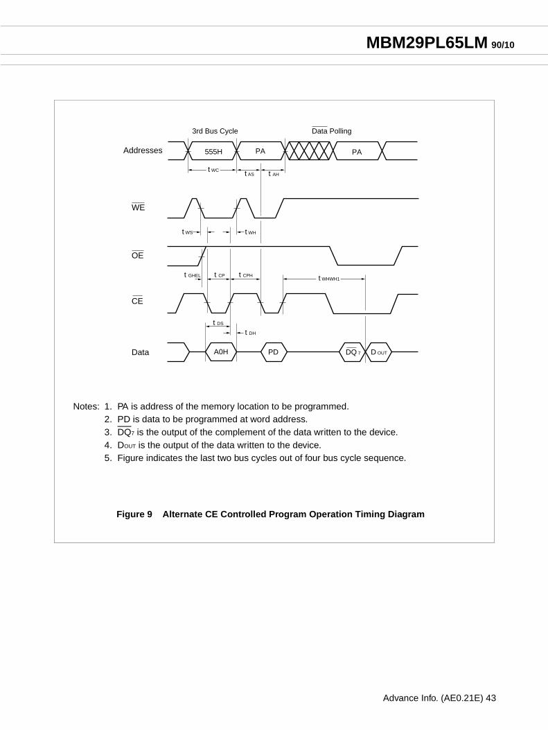
MBM29PL65LM 90/10
t CP
t DS
t WHWH1
t WC t AH
WE
OE
Addresses
Data
t AS
t CPH
t DH
DQ 7A0H D OUT
CE
555H PA PA
Data Polling3rd Bus Cycle
t WS t WH
t GHEL
PD
Notes: 1. PA is address of the memory location to be programmed.2. PD is data to be programmed at word address.3. DQ7 is the output of the complement of the data written to the device.4. DOUT is the output of the data written to the device.5. Figure indicates the last two bus cycles out of four bus cycle sequence.
Figure 9 Alternate CE Controlled Program Operation Timing Diagram
Advance Info. (AE0.21E) 43

44
MBM29PL65LM 90/10
Address
Data
VCC
CE
OE
WE
555h 2AAh 555h 555h 2AAh SA*
tWCtAS tAH
tCS
tGHWL
tCH
tWP
tDS
tVCS
tDH
tWPH
AAh 55h 80h AAh 55h 30h
10h for Chip Erase
SA*
30h
tTOW
* SA is the sector address for Sector Erase. Addresses = 555h (Word) for Chip Erase.
Figure 10 Chip/Sector Erase Operation Timing Diagram
(AE0.21E) Advance Info.

MBM29PL65LM 90/10
Figure 11 Erase Suspend Operation Timing Diagram
Address
Data
CE
WE
XXXh
tWC
tCS tCH
tWP
tDS
B0h
RY/BY
tSPD
Advance Info. (AE0.21E) 45
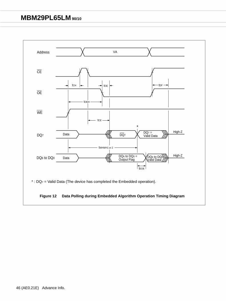
46
MBM29PL65LM 90/10
tOEH
tCH tOE
tCE
tDF
tEOE
tWHWH1 or 2
CE
DQ7
DQ6 to DQ0
DQ7DQ7 =Valid Data
DQ6 to DQ0 =Output Flag
DQ6 to DQ0Valid Data
OE
WE
Address
High-Z
High-ZData
Data
*
VA
* : DQ7 = Valid Data (The device has completed the Embedded operation).
Figure 12 Data Polling during Embedded Algorithm Operation Timing Diagram
(AE0.21E) Advance Info.

MBM29PL65LM 90/10
* : DQ6 stops toggling (The device has completed the Embedded operation).
tDHtOE tCE
CE
WE
OE
DQ 6/DQ2
Address
Data ToggleData
ToggleData
ToggleData
StopToggling
OutputValid
*
tOEHtOEH
tOEPH
tAHT tAHTtASO tAS
tCEPH
Figure 13 Toggle Bit l Timing Diagramduring Embedded Algorithm Operations
* : DQ2 is read from the erase-suspended sector.
DQ2*
DQ6
Figure 14 DQ 2 vs. DQ 6
WE Erase
EraseSuspend
EnterEmbedded
Erasing
Erase SuspendRead
Enter EraseSuspend Program
EraseSuspendProgram
Erase SuspendRead
EraseResume
Erase EraseComplete
ToggleDQ2 and DQ6 with OE or CE
Advance Info. (AE0.21E) 47
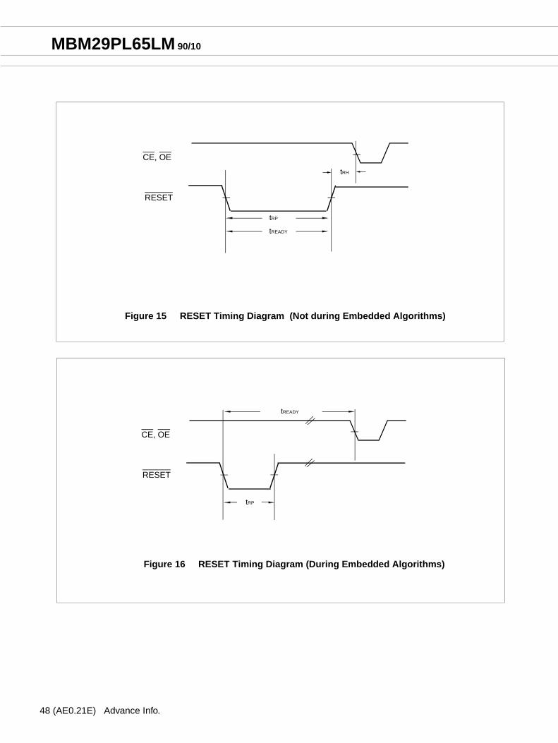
48
MBM29PL65LM 90/10
Figure 15 RESET Timing Diagram (Not during Embedded Algorithms)
RESET
tREADY
CE, OE
tRH
tRP
RESET
CE, OE
Figure 16 RESET Timing Diagram (During Embedded Algorithms)
tRP
tREADY
(AE0.21E) Advance Info.
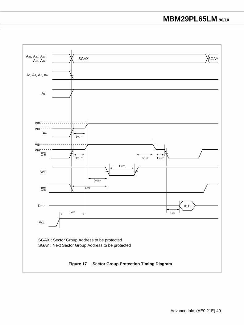
MBM29PL65LM 90/10
t VLHT
SGAXA21, A20, A19
A18, A17SGAY
A6, A3, A2, A0
A9
VIH
t VLHT
OEVIH
t VLHTt VLHT
t OESP
t WPP
t CSP
WE
CE
t OE
01HData
VCC
A1
t VCS
VID
VID
SGAX : Sector Group Address to be protectedSGAY : Next Sector Group Address to be protected
Figure 17 Sector Group Protection Timing Diagram
Advance Info. (AE0.21E) 49
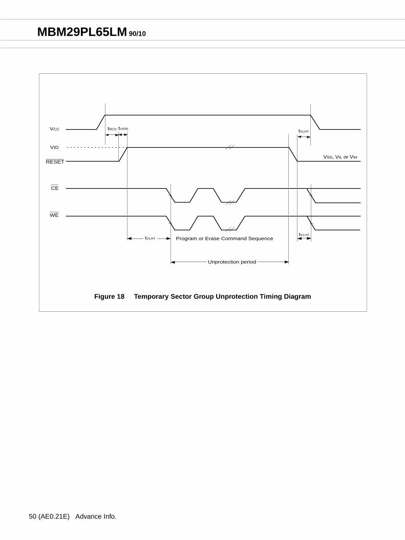
50
MBM29PL65LM 90/10
RESET
CE
WE
tVLHT Program or Erase Command SequencetVLHT
tVIDR
VID
Unprotection period
tvCS tVLHTVCC
VSS, VIL or VIH
Figure 18 Temporary Sector Group Unprotection Timing Diagram
(AE0.21E) Advance Info.

MBM29PL65LM 90/10
SGAX: Sector Group Address to be protectedSGAY : Next Sector Group Address to be protectedTIME-OUT : Time-Out window = 250 µs (min)
SGAY
RESET
OE
WE
CE
Data
A1
VCC
A6, A3, A2, A0
Add SGAXSGAX
60h01h40h60h60h
TIME-OUT
tVCS
tVLHT
tVIDR
tOE
Figure 19 Extended Sector Group Protection Timing Diagram
Advance Info. (AE0.21E) 51

52
MBM29PL65LM 90/10
VCC
CE
WE
tVLHT Program Command SequencetVLHT
tVCS
tVACCR
VACC
tVLHT
Acceleration period
ACC
Figure 20 Accelerated Program Timing Diagram
(AE0.21E) Advance Info.

MBM29PL65LM 90/10
nnnn FLOW CHART
EMBEDDED ALGORITHMS
555h/AAh
555h/A0h
2AAh/55h
Program Address/Program Data
Programming Completed
Last Address?
Increment Address
Verify Data?
Data Polling
Program Command Sequence (Address/Command):
Write ProgramCommand Sequence
(See Below)
Start
No
No
Yes
Yes
EmbeddedProgramAlgorithmin program
Figure 21 Embedded Program TM Algorithm
Advance Info. (AE0.21E) 53
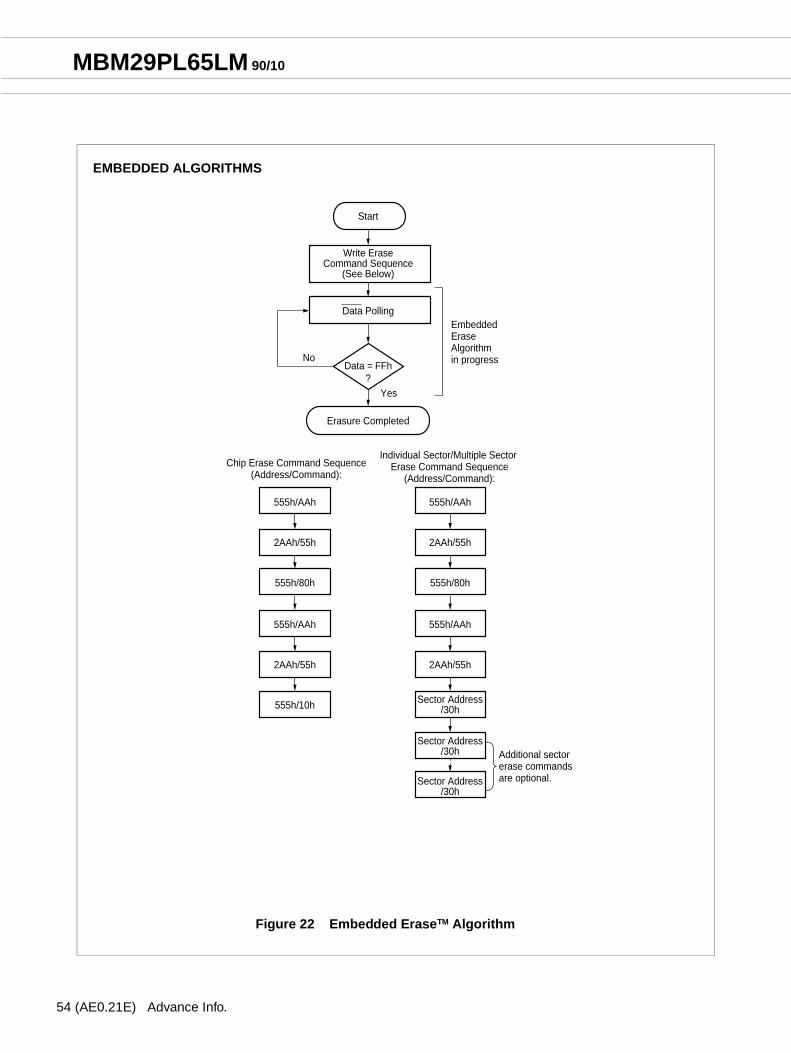
54
MBM29PL65LM 90/10
EMBEDDED ALGORITHMS
555h/AAh
555h/80h
2AAh/55h
555h/AAh
555h/10h
2AAh/55h
555h/AAh
555h/80h
2AAh/55h
555h/AAh
Sector Address/30h
Sector Address/30h
Sector Address/30h
2AAh/55h
Erasure Completed
Data = FFh?
Data Polling
Write EraseCommand Sequence
(See Below)
Start
No
Yes
EmbeddedEraseAlgorithmin progress
Chip Erase Command Sequence(Address/Command):
Individual Sector/Multiple Sector Erase Command Sequence
(Address/Command):
Additional sectorerase commandsare optional.
Figure 22 Embedded Erase TM Algorithm
(AE0.21E) Advance Info.

MBM29PL65LM 90/10
DQ 7 = Data? *
No
No
DQ 7 = Data?
DQ 5 = 1?
Yes
Yes
No
Read Byte(DQ 7 to DQ 0)
Addr. = VA
Read Byte(DQ 7 to DQ 0)
Addr. = VA
Yes
Start
Fail Pass
* : DQ7 is rechecked even if DQ5 = “1” because DQ7 may change simultaneously with DQ5.
VA = Valid address for programming= Any of the sector addresses within
the sector being erased during sector erase or multiple sector erases operation
= Any of the sector addresses within the sector not being protected during chip erase operation
Figure 23 Data Polling Algorithm
Advance Info. (AE0.21E) 55
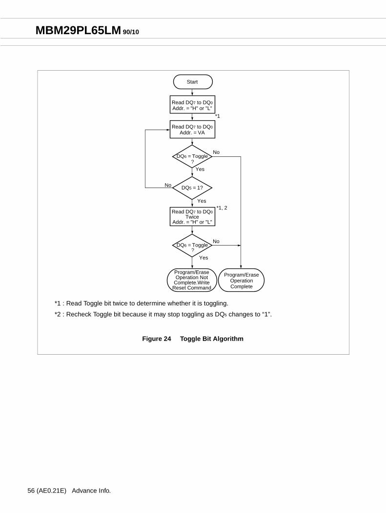
56
MBM29PL65LM 90/10
*1 : Read Toggle bit twice to determine whether it is toggling.
*2 : Recheck Toggle bit because it may stop toggling as DQ5 changes to “1”.
DQ6 = Toggle
DQ5 = 1?
Read DQ7 to DQ0
Addr. = "H" or "L"
Read DQ7 to DQ0
Addr. = VA
Read DQ7 to DQ0Twice
Addr. = "H" or "L"
Start
No
No
No
Yes
Yes
Yes
*1
*1, 2
Program/EraseOperation Not
Complete.WriteReset Command
Program/EraseOperationComplete
DQ6 = Toggle
?
?
Figure 24 Toggle Bit Algorithm
(AE0.21E) Advance Info.

MBM29PL65LM 90/10
Start
NoNo
No
Yes
Yes Yes
Data = 01h?
Device Failed
PLSCNT = 25?
PLSCNT = 1
Remove VID from A9
Write Reset Command
Remove VID from A9
Write Reset Command
Sector Group ProtectionCompleted
Protect Another SectorGroup?
Increment PLSCNT
Read from Sector GroupAddr. = SGA, A1 = VIHA6 = A3 = A2 = A0 = VIL
Setup Sector Group Addr.(A20, A19, A18, A17)
OE = VID, A9 = VID
CE = VIL, RESET = VIH
A6 = A3 = A2 = A0 = VIL, A1 = VIH
Activate WE Pulse
Time out 100 µs
WE = VIH, CE = OE = VIL
(A9 should remain VID)
( )
Figure 25 Sector Group Protection Algorithm
Advance Info. (AE0.21E) 57
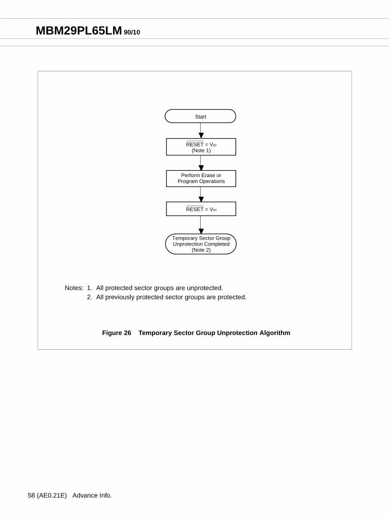
58
MBM29PL65LM 90/10
RESET = VID
(Note 1)
Perform Erase orProgram Operations
RESET = VIH
Start
Temporary Sector GroupUnprotection Completed
(Note 2)
Notes: 1. All protected sector groups are unprotected.2. All previously protected sector groups are protected.
Figure 26 Temporary Sector Group Unprotection Algorithm
(AE0.21E) Advance Info.

MBM29PL65LM 90/10
To Protect Sector Group
Yes
No
No
PLSCNT = 1
Protection Other Sector
Start
Sector Group Protection
Extended Sector Group
Completed
Remove VID from RESETWrite Reset Command
RESET = VID
Wait to 4 µs
Protection Entry?
To Setup Sector Group Protection Write XXXh/60h
Write 60h to Sector Address(A6 = A3 = A2 = A0 =VIL, A1 = VIH)
Time Out 250 µs
To Verify Sector Group ProtectionWrite 40h to Sector Address
(A6 = A3 = A2 = A0 =VIL, A1 = VIH)
Data = 01h?
Group ?
Device is Operating inTemporary Sector Group
Read from Sector Group
(A6 = A3 = A2 = A0 =VIL, A1 = VIH)
Increment PLSCNT
No
Yes
Yes
Unprotection Mode
Address
Setup Next Sector GroupAddress
No
Yes
PLSCNT = 25?
Device Failed
Remove VID from RESETWrite Reset Command
Figure 27 Extended Sector Group Protection Algorithm
Advance Info. (AE0.21E) 59

60
MBM29PL65LM 90/10
FAST MODE ALGORITHM
Start
555h/AAh
2AAh/55h
XXXh/A0h
555h/20h
Verify Data?No
Program Address/Program Data
Data Polling
Last Address?
Programming Completed
XXXh/90h
XXXh/F0h
Increment AddressNo
Yes
Yes
Set Fast Mode
In Fast Program
Reset Fast Mode
Figure 28 Embedded Program TM Algorithm for Fast Mode
(AE0.21E) Advance Info.
MBM29PL65LM 90/10
nnnn ORDERING INFORMATION
Standard Products
Fujitsu standard products are available in several packages. The order number is formed by a combination of:
MBM29PL65LM 90 TN
DEVICE NUMBER/DESCRIPTION64 Mega-bit (4M × 16) MirrorFlash with Page Mode,Uniform Sector Bottom WP 3.0 V-only Read, Program, and Erase
PACKAGE TYPETN = 48-Pin Thin Small Outline Package
(TSOP(I)) Standard Pinout
SPEED OPTION
90 = 90ns access time
10 = 100ns access time
Advance Info. (AE0.21E) 61

MBM29PL65LM 90/10
nnnn PACKAGE DIMENSIONS
–.003+.001
–0.08+0.03
.007
0.17
"A"
(Stand off height)0.10(.004)
(Mountingheight)
(.472±.008)12.00±0.20*
*
LEAD No.
48
2524
1
(.004±.002)
0.10(.004) M
1.10+0.10–0.05
+.004–.002.043
0.10±0.05
(.009±.002)0.22±0.05
TYP0.50(.020)
(.453)11.50REF
(.787±.008)20.00±0.20
(.724±.008)18.40±0.20
INDEX
2001 FUJITSU LIMITED F48029S-c-4-5C
0~8˚
0.25(.010)
0.60±0.15(.024±.006)
Details of "A" part
48-pin plastic TSOP(I)(FPT-48P-M19)
MBM29PL65LM 90/10
notice. sales
t arens, ande. Also,ent ofthe use
velopedcluding use,evelopeding fatald, could death,
nuclearaffic
missileuiringtificial
/or anyn with
re. Youres by
y andntion ofs.
ods order thee prior export
FUJITSU LIMITEDFor further information please contact:
Japan
FUJITSU LIMITEDMarketing DivisionElectronic DevicesShinjuku Dai-Ichi Seimei Bldg. 7-1,Nishishinjuku 2-chome, Shinjuku-ku,Tokyo 163-0721, JapanTel: +81-3-5322-3353Fax: +81-3-5322-3386http://edevice.fujitsu.com/
North and South America
FUJITSU MICROELECTRONICS AMERICA, INC.3545 North First Street,San Jose, CA 95134-1804, U.S.A.Tel: +1-408-922-9000Fax: +1-408-922-9179Customer Response CenterMon. - Fri.: 7 am - 5 pm (PST)Tel: +1-800-866-8608Fax: +1-408-922-9179http://www.fma.fujitsu.com/
Europe
FUJITSU MICROELECTRONICS EUROPE GmbHAm Siebenstein 6-10,D-63303 Dreieich-Buchschlag,GermanyTel: +49-6103-690-0Fax: +49-6103-690-122http://www.fme.fujitsu.com/
Asia Pacific
FUJITSU MICROELECTRONICS ASIA PTE. LTD.#05-08, 151 Lorong Chuan,New Tech Park,Singapore 556741Tel: +65-281-0770Fax: +65-281-0220http://www.fmal.fujitsu.com/
Korea
FUJITSU MICROELECTRONICS KOREA LTD.1702 KOSMO TOWER, 1002 Daechi-Dong,Kangnam-Gu,Seoul 135-280KoreaTel: +82-2-3484-7100Fax: +82-2-3484-7111
F0210 FUJITSU LIMITED Printed in Japan
All Rights Reserved.
The contents of this document are subject to change withoutCustomers are advised to consult with FUJITSU representatives before ordering.
The information and circuit diagrams in this documenpresented as examples of semiconductor device applicatioare not intended to be incorporated in devices for actual usFUJITSU is unable to assume responsibility for infringemany patent rights or other rights of third parties arising from of this information or circuit diagrams.
The products described in this document are designed, deand manufactured as contemplated for general use, inwithout limitation, ordinary industrial use, general officepersonal use, and household use, but are not designed, dand manufactured as contemplated (1) for use accompanyrisks or dangers that, unless extremely high safety is securehave a serious effect to the public, and could lead directly topersonal injury, severe physical damage or other loss (i.e.,reaction control in nuclear facility, aircraft flight control, air trcontrol, mass transport control, medical life support system,launch control in weapon system), or (2) for use reqextremely high reliability (i.e., submersible repeater and arsatellite).Please note that Fujitsu will not be liable against you andthird party for any claims or damages arising in connectioabove-mentioned uses of the products.
Any semiconductor devices have an inherent chance of failumust protect against injury, damage or loss from such failuincorporating safety design measures into your facilitequipment such as redundancy, fire protection, and preveover-current levels and other abnormal operating condition
If any products described in this document represent gotechnologies subject to certain restrictions on export unForeign Exchange and Foreign Trade Law of Japan, thauthorization by Japanese government will be required forof those products from Japan.
Advance Info. (AE0.21E) 63