Embed Size (px)
Citation preview
MIPS32® M5150 Processor Core Family Datasheet February 25, 2015
MIPS32® M5150 Processor Core Family Datasheet, Revision 01.01 MD00977
Copyright © 2012, 2013 Imagination Technologies Ltd. and/or its affiliated group companies. All rights reserved.
MIPSVerified™
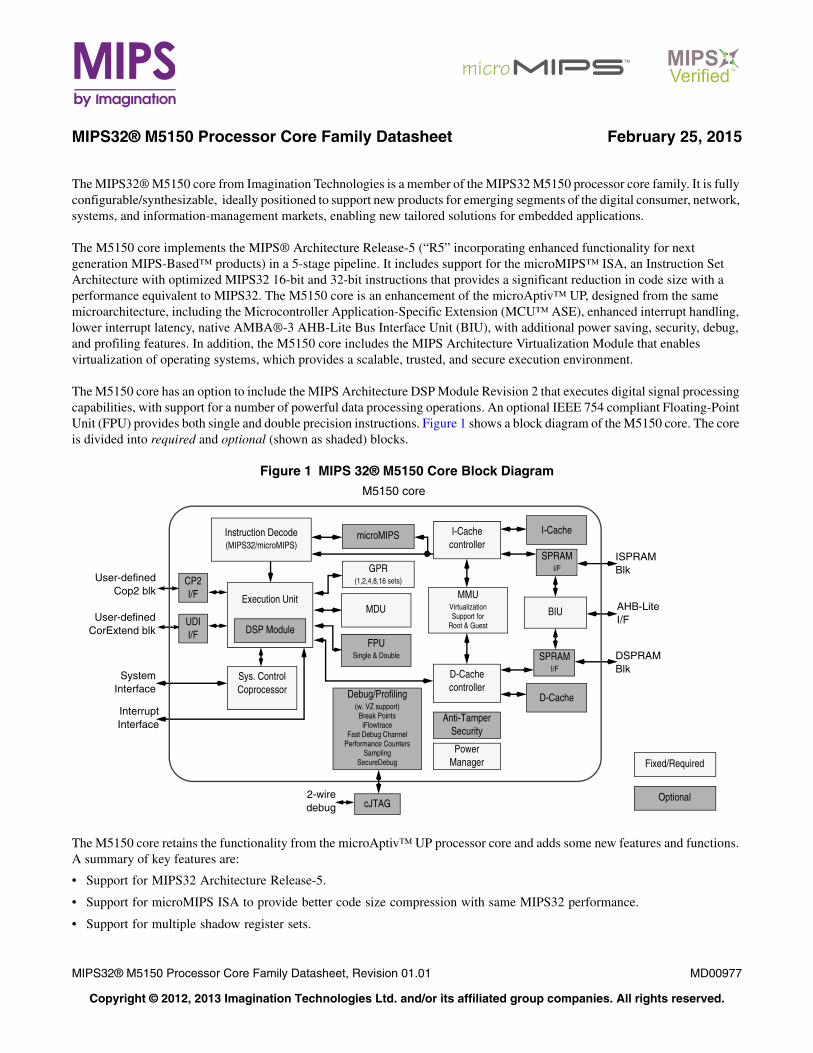
The MIPS32® M5150 core from Imagination Technologies is a member of the MIPS32 M5150 processor core family. It is fully configurable/synthesizable, ideally positioned to support new products for emerging segments of the digital consumer, network, systems, and information-management markets, enabling new tailored solutions for embedded applications.
The M5150 core implements the MIPS® Architecture Release-5 (“R5” incorporating enhanced functionality for next generation MIPS-Based™ products) in a 5-stage pipeline. It includes support for the microMIPS™ ISA, an Instruction Set Architecture with optimized MIPS32 16-bit and 32-bit instructions that provides a significant reduction in code size with a performance equivalent to MIPS32. The M5150 core is an enhancement of the microAptiv™ UP, designed from the same microarchitecture, including the Microcontroller Application-Specific Extension (MCU™ ASE), enhanced interrupt handling, lower interrupt latency, native AMBA®-3 AHB-Lite Bus Interface Unit (BIU), with additional power saving, security, debug, and profiling features. In addition, the M5150 core includes the MIPS Architecture Virtualization Module that enables virtualization of operating systems, which provides a scalable, trusted, and secure execution environment.
The M5150 core has an option to include the MIPS Architecture DSP Module Revision 2 that executes digital signal processing capabilities, with support for a number of powerful data processing operations. An optional IEEE 754 compliant Floating-Point Unit (FPU) provides both single and double precision instructions. Figure 1 shows a block diagram of the M5150 core. The core is divided into required and optional (shown as shaded) blocks.
Figure 1 MIPS 32® M5150 Core Block Diagram
The M5150 core retains the functionality from the microAptiv™ UP processor core and adds some new features and functions. A summary of key features are:
• Support for MIPS32 Architecture Release-5.
• Support for microMIPS ISA to provide better code size compression with same MIPS32 performance.
• Support for multiple shadow register sets.
Fixed/Required
Optional
DSPRAMBlk
AHB-LiteI/F
CP2I/F
Sys. Control Coprocessor
UDII/F
GPR(1,2,4,8,16 sets)
Debug/Profiling(w. VZ support)
Break PointsiFlowtrace
Fast Debug ChannelPerformance Counters
SamplingSecureDebug
microMIPS I-Cachecontroller
D-Cachecontroller
User-definedCop2 blk
User-definedCorExtend blk
SystemInterface
InterruptInterface
BIU
ISPRAMBlk
Instruction Decode(MIPS32/microMIPS)
cJTAG2-wiredebug
D-Cache
M5150 core
I-Cache
SPRAMI/F
SPRAMI/F
Power Manager
Anti-Tamper Security
MMUVirtualizationSupport for
Root & Guest
Execution UnitMDU
FPUSingle & Double
DSP Module
2 MIPS32® M5150 Processor Core Family Datasheet, Revision 01.01
Copyright © 2012, 2013 Imagination Technologies Ltd. and/or its affiliated group companies. All rights reserved.
• The Memory Management Unit (MMU), selectable between a Translation Lookaside Buffer (TLB) or a simple Fixed Mapping Translation (FMT) mechanism.
• Supports configurable DSP Module Revision 2 for digital signal processing capabilities.
• Multiply/Divide Unit (MDU) - If the DSP is not included, the MDU can be configured for either performance or area optimizations. The high-performance optimization supports a single-cycle 32x16-bit MAC instruction or two-cycle 32x32-bit instructions. If the DSP is included, the MDU is enhanced with a hardware multiplier array supporting single-cycle 32x32 MAC and DSP instructions.
• Floating-Point Unit (FPU), an IEEE-754 compliant Floating-Point Unit with single and double precision datatypes.
• Instruction and data caches are fully configurable from 0 to 64 Kbytes in size. In addition, each cache can be organized as direct-mapped or 2-way, 3-way, or 4-way set associative. Load and fetch cache misses only block until the critical word becomes available. The pipeline resumes execution while the remaining words are being written to the cache. Both caches are virtually indexed and physically tagged to allow them to be accessed in the same clock in which the address is translated.
• Support for the MCU ASE to enhance common functions used in microcontroller applications such as interrupts and semaphore manipulation.
• Security feature such as the SecureDebug to restrict untrusted EJTAG debug access.
• Support for the Virtualization Module via privileged (root) and unprivileged (guest) operating modes. Legacy software will run in guest mode where all operations are monitored and trapped by hypervisor software if the guest does not behave as expected. The hypervisor operates invisibly to the guest, and enforces data protection between guests.
• AMBA-3 AHB-Lite bus interface.
• Parity support.
• An optional Enhanced JTAG (EJTAG version 4.52) block allows for single-stepping of the processor as well as instruction and data virtual address/value breakpoints. iFlowtrace™ version 2.0 is also supported to add real-time instruction program counter and special events trace capability for debug. Additionally, Fast Debug Channel, Performance Counters, and PC/Data sampling functions are added to enrich debug and profiling features on the M5150 core.
• External block to convert 4-wire EJTAG (IEEE 1149.1) interface to 2-wire cJTAG (IEEE 1149.7) interface.
• Configurable hardware breakpoints triggered by address match or address range.
Features• 5-stage pipeline
• 32-bit Address and Data Paths
• MIPS32 Instruction Set Architecture
• MIPS32 Enhanced Architecture Features
• Vectored interrupts and support for external inter-rupt controller
• Programmable exception vector base
• Atomic interrupt enable/disable
• GPR shadow registers (one, three, seven, or fifteen additional shadows can be optionally added to min-imize latency for interrupt handlers)
• Bit field manipulation instructions
• Virtual memory support (smaller page sizes and hooks for more extensive page table manipulation)
• microMIPS Instruction Set Architecture
• microMIPS ISA is a build-time configurable option that reduces code size over MIPS32, while main-taining MIPS32 performance.
• Combining both 16-bit and 32-bit opcodes, micro-MIPS supports all MIPS32 instructions (except branch-likely instructions) with new optimized encoding. Frequently used MIPS32 instructions are available as 16-bit instructions.
• Added fifteen new 32-bit instructions and thirty-nine 16-bit instructions.
• Stack pointer implicit in instruction.
• MIPS32 assembly and ABI-compatible.
• Supports MIPS architecture Modules and User-defined Instructions (UDIs).
• MCU™ ASE
• Increases the number of interrupt hardware inputs from 6 to 8 for Vectored Interrupt (VI) mode, and from 63 to 255 for External Interrupt Controller (EIC) mode.
• Separate priority and vector generation. 16-bit vec-tor address is provided.
• Hardware assist combined with the use of Shadow Register Sets to reduce interrupt latency during the prologue and epilogue of an interrupt.
MIPS32® M5150 Processor Core Family Datasheet, Revision 01.01 3
Copyright © 2012, 2013 Imagination Technologies Ltd. and/or its affiliated group companies. All rights reserved.
• An interrupt return with automated interrupt epi-logue handling instruction (IRET) improves inter-rupt latency.
• Supports optional interrupt chaining.
• Two memory-to-memory atomic read-modify-write instructions (ASET and ACLR) eases commonly used semaphore manipulation in microcontroller applications. Interrupts are automatically disabled during the operation to maintain coherency.
• Programmable Cache Sizes
• Individually configurable instruction and data caches
• Sizes from 0 - 64KB
• Direct Mapped, 2-, 3-, or 4-Way Set Associative
• Loads block only until critical word is available
• Write-back and write-through support
• 128-bit (16-byte) cache line size, word sectored - suitable for standard 32-bit wide single-port SRAM
• Virtually indexed, physically tagged
• Cache line locking support
• Non-blocking prefetches
• Scratchpad RAM (SPRAM) Support
• Can optionally replace 1 way of the I- and/or D-cache with a fast scratchpad RAM
• Independent external pin interfaces for I- and D-scratchpads
• 20 index address bits allow access of arrays up to 1MB
• Interface allows back-stalling the core
• MIPS32 Privileged Resource Architecture (PRA)
• Count/Compare registers for real-time timerinterrupts
• I and D watch registers for SW breakpoints
• Memory Management Unit
• Simple Fixed Mapping Translation (FMT) mecha-nism, or
• 4-entry instruction and data Translation Lookaside Buffers (ITLB/DTLB) and a 16 or 32 dual-entry joint TLB (JTLB) with variable page sizes. Read, write, and execute page-protection attributes indi-vidually programmable.
• Bus Interface Unit (BIU)
• Supports AMBA-3 AHB-Lite protocol
• All I/O’s fully registered
• Separate unidirectional 32-bit address and data buses
• Two 16-byte collapsing write buffers
• Support for variable CPU and bus clock ratios to allow the bus to run at a lower speed than the CPU.
• Virtualization Module Support
• Support for the Virtualization Module using “trap and emulate” techniques.
• Two new operating modes: privileged (root) and unprivileged (guest)
• System resources controlled through privileged instructions while executing in privileged mode
• Execution of a privileged instruction in unprivi-leged mode will cause an exception (trap), returning control to privileged-mode software
• Address translation is performed on the entire address space when in unprivileged mode
• Configurable from 1 to 7 guests
• Supports both RTLB (Root TLB) and RPU (Root Protection Unit) memory management units
• Parity Support
• The I-cache, D-cache, ISPRAM, and DSPRAM support optional parity detection.
• MIPS DSP Module (Revision 2.0)
• Support for MAC operations with 3 additional pairs of Hi/Lo accumulator registers (Ac0 - Ac3)
• Fractional data types (Q15, Q31) with rounding support
• Saturating arithmetic with overflow handling
• SIMD instructions operate on 2x16-bit or 4x8-bit operands simultaneously
• Separate MDU pipeline with full-sized hardware multiplier to support back-to-back operations
• The DSP Module is build-time configurable.
• Multiply/Divide Unit (high-performance configuration without DSP)
• Maximum issue rate of one 32x16 multiply per clock via on-chip 32x16 hardware multiplier array.
• Maximum issue rate of one 32x32 multiply every other clock
• Early-in iterative divide. Minimum 11 and maxi-mum 34 clock latency (dividend (rs) sign exten-sion-dependent)
• Multiply/Divide Unit (with DSP configuration)
• Maximum issue rate of one 32x32 multiply per clock via on-chip 32x32 hardware multiplier array
• Maximum issue rate of one 32x32 multiply every clock
4 MIPS32® M5150 Processor Core Family Datasheet, Revision 01.01
Copyright © 2012, 2013 Imagination Technologies Ltd. and/or its affiliated group companies. All rights reserved.
• Early-in iterative divide. Minimum 12 and maxi-mum 38clock latency (dividend (rs) sign extension-dependent)
• Multiply/Divide Unit (area-efficient configuration without DSP)
• 32 clock latency on multiply
• 34 clock latency on multiply-accumulate
• 33-35 clock latency on divide (sign-dependent)
• Floating Point Unit (FPU)
• 1985 IEEE-754 compliant Floating Point Unit.
• Supports single and double precision datatypes
• 2008 IEEE-754 compatibility control for NaN han-dling and Abs/Neg instructions
• Runs at 1:1 core/FPU clock ratio.
• The FPU is build-time configurable.
• CorExtend® User-Defined Instruction Set Extensions
• Allows user to define and add instructions to the core at build time
• Maintains full MIPS32 compatibility
• Supported by industry-standard development tools
• Single or multi-cycle instructions
• Coprocessor 2 interface
• 32-bit interface to an external coprocessor
• Anti-Tamper Security Features
• Injection of random pipeline slips controlled via CP0 register
• Fast general-purpose 32-bit pseudo random genera-tor accessible via CP0 register
• User defined cache/SPRAM scrambling (config-ured via CP0 register)
• Complex pseudo random generator for hardware use controlled via user-defined seed
• Power Control
• Minimum frequency: 0 MHz
• Power-down mode (triggered by WAIT instruction)
• Support for software-controlled clock divider
• Support for extensive use of local gated clocks
• Optional power-saving mode in organizing individ-ual cache memory array per way
• EJTAG Debug/Profiling and iFlowtrace™ Mechanism
• CPU control with start, stop, and single stepping
• Virtual instruction and data address/value break-points
• Hardware breakpoint supports both address match and address range triggering
• Optional simple hardware breakpoints on virtual addresses; 8I/4D, 6I/2D, 4I/2D, 2I/1D breakpoints, or no breakpoints
• Optional complex hardware breakpoints with 8I/4D, 6I/2D simple breakpoints
• TAP controller is chainable for multi-CPU debug
• Supports EJTAG (IEEE 1149.1) and compatible with cJTAG 2-wire (IEEE 1149.7) extension proto-col
• Cross-CPU breakpoint support
• iFlowtrace support for real-time instruction PC and special events
• PC and/or load/store address sampling for profiling
• Performance Counters
• Support for Fast Debug Channel (FDC)
• SecureDebug
• An optional feature that disables access via EJTAG in an untrusted environment
• Testability
• Full scan design achieves test coverage in excess of 99% (dependent on library and configuration options)
• Optional memory BIST for internal SRAM arrays. Two memory BIST algorithms are provided and selectable by input pin.
Architecture Overview
The M5150 core contains both required and optional blocks, as shown in Figure 1. Required blocks must be implemented to remain MIPS-compliant. Optional blocks can be added to the M5150 core based on the needs of the implementation.
The required blocks are as follows:
• Instruction Decode
• Execution Unit
• General Purposed Registers (GPR)
• Multiply/Divide Unit (MDU)
• System Control Coprocessor (CP0)
• Memory Management Unit (MMU)
• I/D Cache Controllers
• Bus Interface Unit (BIU)
• Power Management
Optional or configurable blocks include:
• Instruction Cache
MIPS32® M5150 Processor Core Family Datasheet, Revision 01.01 5
Copyright © 2012, 2013 Imagination Technologies Ltd. and/or its affiliated group companies. All rights reserved.
• Data Cache
• Scratchpad RAM interface
• Configurable instruction decoder supporting three ISA modes: MIPS32-only, MIPS32 and microMIPS, or microMIPS-only
• DSP (integrated with MDU)
• Floating-point Unit (FPU)
• Virtualization support (integrated with MMU)
• Anti-Tamper Security Block
• Coprocessor 2 interface
• CorExtend® User-Defined Instruction (UDI) interface
• Debug/Profiling with Enhanced JTAG (EJTAG) Controller, Break points, Sampling, Performance counters, Fast Debug Channel, and iFlowtrace logic
The section "MIPS32® M5150 Core Required Logic Blocks" on page 6 discusses the required blocks. The section "MIPS32® M5150 Core Optional or Configurable Logic Blocks" on page 13 discusses the optional blocks.
Pipeline Flow
The M5150 core implements a 5-stage pipeline with a performance similar to the microAptiv™ UP pipeline. The pipeline allows the processor to achieve high frequency while minimizing device complexity, reducing both cost and power consumption.
The M5150 core pipeline consists of five stages:
• Instruction (I Stage)
• Execution (E Stage)
• Memory (M Stage)
• Align (A Stage)
• Writeback (W stage)
The M5150 core implements a bypass mechanism that allows the result of an operation to be forwarded directly to the instruction that needs it without having to write the result to the register and then read it back.
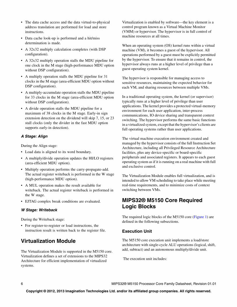
Figure 2 shows a timing diagram of the M5150 core pipeline (shown with the-high performance MDUand TLB used in the MMU).
Figure 2 MIPS32® M5150 Core Pipeline
I Stage: Instruction Fetch
During the Instruction fetch stage:
• An instruction is fetched from the instruction cache.
• The I-TLB performs a virtual-to-physical address translation.
• If both MIPS32 and microMIPS ISAs are supported, microMIPS instructions are converted to MIPS32-like instructions. If the MIPS32 ISA is not supported, 16-bit microMIPS instructions will be first recoded into 32-bit microMIPS equivalent instructions, and then decoded in native microMIPS ISA format.
E Stage: Execution
During the Execution stage:
• Operands are fetched from the register file.
• Operands from the M and A stage are bypassed to this stage.
• The Arithmetic Logic Unit (ALU) begins the arithmetic or logical operation for register-to-register instructions.
• The ALU calculates the virtual data address for load and store instructions.
• The ALU determines whether the branch condition is true and calculates the virtual branch target address for branch instructions.
• Instruction logic selects an instruction address.
• All multiply and divide operations begin in this stage.
M Stage: Memory Fetch
During the Memory fetch stage:
• The arithmetic ALU operation completes.
I E M A W
I-TLB
I-A1
I-Cache RegRd
I Dec
ALU Op
D-TLB
D-Cache Align RegWD-AC
BypassBypass
Mult RegW
Bypass
Acc
I-A2
Div RegWAcc
6 MIPS32® M5150 Processor Core Family Datasheet, Revision 01.01
Copyright © 2012, 2013 Imagination Technologies Ltd. and/or its affiliated group companies. All rights reserved.
• The data cache access and the data virtual-to-physical address translation are performed for load and store instructions.
• Data cache look-up is performed and a hit/miss determination is made.
• A 32x32 multiply calculation completes (with DSP configuration).
• A 32x32 multiply operation stalls the MDU pipeline for one clock in the M stage (high-performance MDU option without DSP configuration).
• A multiply operation stalls the MDU pipeline for 31 clocks in the M stage (area-efficient MDU option without DSP configuration).
• A multiply-accumulate operation stalls the MDU pipeline for 33 clocks in the M stage (area-efficient MDU option without DSP configuration).
• A divide operation stalls the MDU pipeline for a maximum of 38 clocks in the M stage. Early-in sign extension detection on the dividend will skip 7, 15, or 23 stall clocks (only the divider in the fast MDU option supports early-in detection).
A Stage: Align
During the Align stage:
• Load data is aligned to its word boundary.
• A multiply/divide operation updates the HI/LO registers (area-efficient MDU option).
• Multiply operation performs the carry-propagate-add. The actual register writeback is performed in the W stage (high-performance MDU option).
• A MUL operation makes the result available for writeback. The actual register writeback is performed in the W stage.
• EJTAG complex break conditions are evaluated.
W Stage: Writeback
During the Writeback stage:
• For register-to-register or load instructions, the instruction result is written back to the register file.
Virtualization Module
The Virtualization Module is supported in the M5150 core. Virtualization defines a set of extensions to the MIPS32 Architecture for efficient implementation of virtualized systems.
Virtualization is enabled by software—the key element is a control program known as a Virtual Machine Monitor (VMM) or hypervisor. The hypervisor is in full control of machine resources at all times.
When an operating system (OS) kernel runs within a virtual machine (VM), it becomes a guest of the hypervisor. All operations performed by a guest must be explicitly permitted by the hypervisor. To ensure that it remains in control, the hypervisor always runs at a higher level of privilege than a guest operating system kernel.
The hypervisor is responsible for managing access to sensitive resources, maintaining the expected behavior for each VM, and sharing resources between multiple VMs.
In a traditional operating system, the kernel (or supervisor) typically runs at a higher level of privilege than user applications. The kernel provides a protected virtual-memory environment for each user application, inter-process communications, IO device sharing and transparent context switching. The hypervisor performs the same basic functions in a virtualized system, except that the hypervisor’s clients are full operating systems rather than user applications.
The virtual machine execution environment created and managed by the hypervisor consists of the full Instruction Set Architecture, including all Privileged Resource Architecture facilities, plus any device-specific or board-specific peripherals and associated registers. It appears to each guest operating system as if it is running on a real machine with full and exclusive control.
The Virtualization Module enables full virtualization, and is intended to allow VM scheduling to take place while meeting real-time requirements, and to minimize costs of context switching between VMs.
MIPS32® M5150 Core Required Logic Blocks
The required logic blocks of the M5150 core (Figure 1) are defined in the following subsections.
Execution Unit
The M5150 core execution unit implements a load/store architecture with single-cycle ALU operations (logical, shift, add, subtract) and an autonomous multiply/divide unit.
The execution unit includes:
MIPS32® M5150 Processor Core Family Datasheet, Revision 01.01 7
Copyright © 2012, 2013 Imagination Technologies Ltd. and/or its affiliated group companies. All rights reserved.
• Arithmetic Logic Unit (ALU) for performing arithmetic and bitwise logical operations. Shared adder for arithmetic operations, load/store address calculation, and branch target calculation.
• Address unit for calculating the next PC and next fetch address selection muxes.
• Load Aligner.
• Shifter and Store Aligner.
• Branch condition comparator.
• Trap condition comparator.
• Bypass muxes to advance result between two adjacent instructions with data dependency.
• Leading Zero/One detect unit for implementing the CLZ and CLO instructions.
• Actual execution of the Atomic Instructions defined in the MCU ASE.
• A separate DSP ALU and Logic block for performing part of DSP Module instructions, such as arithmetic/shift/compare operations if the DSP function is configured.
General Purpose Registers
The M5150 core contains thirty-two 32-bit general-purpose registers used for integer operations and address calculation. Optionally, one, three, seven or fifteen additional register file shadow sets (each containing thirty-two registers) can be added to minimize context switching overhead during interrupt/exception processing. The register file consists of two read ports and one write port and is fully bypassed to minimize operation latency in the pipeline.
Multiply/Divide Unit (MDU)
The M5150 core includes a multiply/divide unit (MDU) that contains a separate, dedicated pipeline for integer multiply/divide operations, and DSP Module multiply instructions. This pipeline operates in parallel with the integer unit (IU) pipeline and does not stall when the IU pipeline stalls. This allows the long-running MDU operations to be partially masked by system stalls and/or other integer unit instructions.
The MIPS architecture defines that the result of a multiply or divide operation be placed in a pair (without DSP enabled) or one of 4 pairs (with DSP enabled) of HI and LO registers. Using the Move-From-HI (MFHI) and Move-From-LO (MFLO) instructions, these values can be transferred to the general-purpose register file.
There are three configuration options for the MDU: 1) a full 32x32 multiplier block; 2) a higher performance 32x16 multiplier block; 3) an area-efficient iterative multiplier
block. Option 2 and 3 are available if the DSP configuration option is disabled. If the DSP configuration option is enabled, option 1 is the default. The selection of the MDU style allows the implementor to determine the appropriate performance and area trade-off for the application.
MDU with 32x32 DSP Multiplier
With the DSP configuration option enabled, the MDU supports execution of one 16x16, 32x16, or 32x32 multiply or multiply-accumulate operation every clock cycle with the built in 32x32 multiplier array. The multiplier is shared with DSP Module operations.
The MDU also implements various shift instructions operating on the HI/LO register and multiply instructions as defined in the DSP Module. It supports all the data types required for this purpose and includes three extra HI/LO registers as defined by the Module.
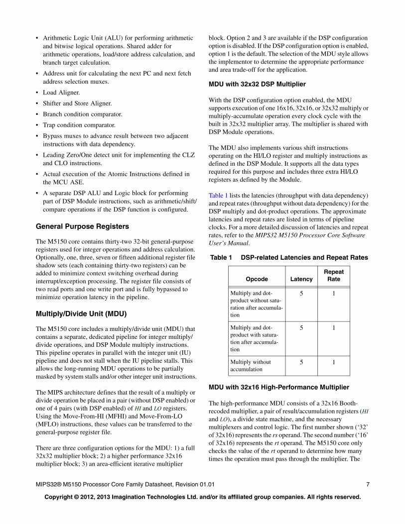
Table 1 lists the latencies (throughput with data dependency) and repeat rates (throughput without data dependency) for the DSP multiply and dot-product operations. The approximate latencies and repeat rates are listed in terms of pipeline clocks. For a more detailed discussion of latencies and repeat rates, refer to the MIPS32 M5150 Processor Core Software User’s Manual.
MDU with 32x16 High-Performance Multiplier
The high-performance MDU consists of a 32x16 Booth-recoded multiplier, a pair of result/accumulation registers (HI and LO), a divide state machine, and the necessary multiplexers and control logic. The first number shown (‘32’ of 32x16) represents the rs operand. The second number (‘16’ of 32x16) represents the rt operand. The M5150 core only checks the value of the rt operand to determine how many times the operation must pass through the multiplier. The
Table 1 DSP-related Latencies and Repeat Rates
Opcode LatencyRepeat
Rate
Multiply and dot-product without satu-ration after accumula-tion
5 1
Multiply and dot-product with satura-tion after accumula-tion
5 1
Multiply without accumulation
5 1
8 MIPS32® M5150 Processor Core Family Datasheet, Revision 01.01
Copyright © 2012, 2013 Imagination Technologies Ltd. and/or its affiliated group companies. All rights reserved.
16x16 and 32x16 operations pass through the multiplier once. A 32x32 operation passes through the multiplier twice.
The MDU supports execution of one 16x16 or 32x16 multiply or multiply-accumulate operation every clock cycle; 32x32 multiply operations can be issued every other clock cycle. Appropriate interlocks are implemented to stall the issuance of back-to-back 32x32 multiply operations. The multiply operand size is automatically determined by logic built into the MDU.
Table 2, Table 3 and Table 4 list the repeat rate (how often the operation can be reissued when there is no data dependency) and latency (number of cycles until a result is available) for the multiply and divide instructions. The approximate latency and repeat rates are listed in terms of pipeline clocks. For a more detailed discussion of latencies and repeat rates, refer to Chapter 2 of the MIPS32 M5150 Processor Core Family Software User’s Manual.
MDU with Area-Efficient Option
With the area-efficient option, multiply and divide operations are implemented with a simple 1-bit-per-clock iterative algorithm. Any attempt to issue a subsequent MDU instruction while a multiply/divide is still active causes an MDU pipeline stall until the operation is completed.
Table 4 lists the latency (number of cycles until a result is available) for the M5150 core multiply and divide instructions. The latencies are listed in terms of pipeline clocks.
Regardless of the multiplier array implementation, divide operations are implemented with a simple 1-bit-per-clock
Table 2 High-Performance Integer Multiply/Divide Unit Latencies and Repeat Rates with DSP
Opcode
Operand Size
(mul rt)(div rs) Latency
RepeatRate
MUL(GPR destination)
16 bits 5 1
32 bits 5 1
MULT, MULTU,MADD, MADDU,MSUB, MSUBU(Hi/Lo destination)
16 bits 5 1
32 bits 5 1
DIV / DIVU(Hi/Lo destination)
8 bits 12-14 / 12 12-14 / 12
16 bits 20-22 / 20 20-22 / 20
24 bits 28-30 / 30 28-30 / 30
32 bits 35-37 / 35 35-37 / 35
Table 3 High-Performance Integer Multiply/Divide Unit Latencies and Repeat Rates without DSP
Opcode
Operand Size
(mul rt)(div rs) Latency
RepeatRate
MUL(GPR destination)
16 bits 5 2
32 bits 6 3
MULT, MULTU,MADD, MADDU,MSUB, MSUBU(Hi/Lo destination)
16 bits 2 1
32 bits 3 2
DIV / DIVU(Hi/Lo destination)
8 bits 11-12 / 11 11-12 / 11
16 bits 19-20 / 19 19-20 / 19
24 bits 27-28 / 27 27-28 / 27
32 bits 34-35 / 34 34-35 / 34
Table 4 Area-Efficient Integer Multiply/Divide Unit Operation Latencies without DSP
Opcode
Operand Size
(mul rt)(div rs) Latency
RepeatRate
MUL(GPR destination)
any 35 32
MULT, MULTU,(Hi/Lo destination)
any 32 32
MADD, MADDU,MSUB, MSUBU(Hi/Lo destination)
any 34 34
DIV / DIVU(Hi/Lo destination)
any 33-34 / 33 33-34 / 33
Table 3 High-Performance Integer Multiply/Divide Unit Latencies and Repeat Rates without DSP
Opcode
Operand Size
(mul rt)(div rs) Latency
RepeatRate
MIPS32® M5150 Processor Core Family Datasheet, Revision 01.01 9
Copyright © 2012, 2013 Imagination Technologies Ltd. and/or its affiliated group companies. All rights reserved.
iterative algorithm. An early-in detection checks the sign extension of the dividend (rs) operand. If rs is 8 bits wide, 23 iterations are skipped. For a 16-bit-wide rs, 15 iterations are skipped, and for a 24-bit-wide rs, 7 iterations are skipped. Any attempt to issue a subsequent MDU instruction while a divide is still active causes an IU pipeline stall until the divide operation has completed.
System Control Coprocessor (CP0)
In the MIPS architecture, CP0 is responsible for the virtual-to-physical address translation and cache protocols, the exception control system, the processor’s diagnostics capability, the operating modes (kernel, user, and debug), and whether interrupts are enabled or disabled. Configuration information, such as cache size and set associativity, presence of build-time options like microMIPS, CorExtend Module or Coprocessor 2 interface, is also available by accessing the CP0 registers.
Coprocessor 0 also contains the logic for identifying and managing exceptions. Exceptions can be caused by a variety of sources, including boundary cases in data, external events, or program errors.
Interrupt Handling
The M5150 core includes support for eight hardware interrupt pins, two software interrupts, and a timer interrupt. These interrupts can be used in any of three interrupt modes, as defined by Release 2 of the MIPS32 Architecture:
• Interrupt compatibility mode, which acts identically to that in an implementation of Release 1 of the Architecture.
• Vectored Interrupt (VI) mode, which adds the ability to prioritize and vector interrupts to a handler dedicated to that interrupt, and to assign a GPR shadow set for use during interrupt processing. The presence of this mode is denoted by the VInt bit in the Config3 register. This mode is architecturally optional; but it is always present on the M5150 core, so the VInt bit will always read as a 1 for the M5150 core.
• External Interrupt Controller (EIC) mode, which redefines the way in which interrupts are handled to provide full support for an external interrupt controller handling prioritization and vectoring of interrupts. The presence of this mode denoted by the VEIC bit in the Config3 register. Again, this mode is architecturally optional. On the M5150 core, the VEIC bit is set externally by the static input, SI_EICPresent, to allow system logic to indicate the presence of an external interrupt controller.
The reset state of the processor is interrupt compatibility mode, such that a processor supporting Release 2 of the Architecture, the M5150 core for example, is fully compatible with implementations of Release 1 of the Architecture.
VI or EIC interrupt modes can be combined with the optional shadow registers to specify which shadow set should be used on entry to a particular vector. The shadow registers further improve interrupt latency by avoiding the need to save context when invoking an interrupt handler.
In the M5150 core, interrupt latency is reduced by:
• Speculative interrupt vector prefetching during the pipeline flush.
• Interrupt Automated Prologue (IAP) in hardware: Shadow Register Sets remove the need to save GPRs, and IAP removes the need to save specific Control Registers when handling an interrupt.
• Interrupt Automated Epilogue (IAE) in hardware: Shadow Register Sets remove the need to restore GPRs, and IAE removes the need to restore specific Control Registers when returning from an interrupt.
• Allow interrupt chaining. When servicing an interrupt and interrupt chaining is enabled, there is no need to return from the current Interrupt Service Routine (ISR) if there is another valid interrupt pending to be serviced. The control of the processor can jump directly from the current ISR to the next ISR without IAE and IAP.
GPR Shadow Registers
The MIPS32 Architecture optionally removes the need to save and restore GPRs on entry to high-priority interrupts or exceptions, and to provide specified processor modes with the same capability. This is done by introducing multiple copies of the GPRs, called shadow sets, and allowing privileged software to associate a shadow set with entry to kernel mode via an interrupt vector or exception. The normal GPRs are logically considered shadow set zero.
The number of GPR shadow sets is a build-time option. The M5150 core allows 1 (the normal GPRs), 2, 4, 8, or 16 shadow sets. The highest number actually implemented is indicated by the SRSCtlHSS field. If this field is zero, only the normal GPRs are implemented.
Shadow sets are new copies of the GPRs that can be substituted for the normal GPRs on entry to kernel mode via an interrupt or exception. Once a shadow set is bound to a kernel-mode entry condition, references to GPRs operate exactly as one would expect, but they are redirected to registers that are dedicated to that condition. Privileged
10 MIPS32® M5150 Processor Core Family Datasheet, Revision 01.01
Copyright © 2012, 2013 Imagination Technologies Ltd. and/or its affiliated group companies. All rights reserved.
software may need to reference all GPRs in the register file, even specific shadow registers that are not visible in the current mode, and the RDPGPR and WRPGPR instructions are used for this purpose. The CSS field of the SRSCtl register provides the number of the current shadow register set, and the PSS field of the SRSCtl register provides the number of the previous shadow register set that was current before the last exception or interrupt occurred.
If the processor is operating in VI interrupt mode, binding of a vectored interrupt to a shadow set is done by writing to the SRSMap register. If the processor is operating in EIC interrupt mode, the binding of the interrupt to a specific shadow set is provided by the external interrupt controller and is configured in an implementation-dependent way. Binding of an exception or non-vectored interrupt to a shadow set is done by writing to the ESS field of the SRSCtl register. When an exception or interrupt occurs, the value of SRSCtlCSS is copied to SRSCtlPSS, and SRSCtlCSS is set to the value taken from the appropriate source. On an ERET, the value of SRSCtlPSS is copied back into SRSCtlCSS to restore the shadow set of the mode to which control returns.
Modes of Operation
The M5150 core implements the Virtualization Module by supporting five modes of operation:
• Guest-user mode is most often used for applications programs.
• Guest-kernel mode is typically used for handling exceptions and operating-system kernel functions, including CP0 management and I/O device accesses.
• Root-user mode is used to run hypervisor (Virtual Machine Monitor (VMM)) user software.
• Root-kernel mode is used to run hypervisor (Virtual Machine Monitor (VMM)) kernel software.
• Debug mode is used during system bring-up and software development. Refer to the EJTAG section for more information on debug mode.
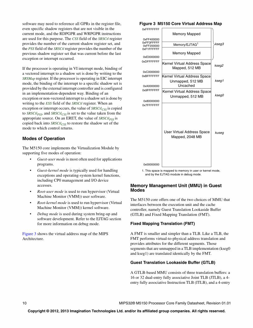
Figure 3 shows the virtual address map of the MIPS Architecture.
Figure 3 M5150 Core Virtual Address Map
Memory Management Unit (MMU) in Guest Modes
The M5150 core offers one of the two choices of MMU that interfaces between the execution unit and the cache controller, namely Guest Translation Lookaside Buffer (GTLB) and Fixed Mapping Translation (FMT).
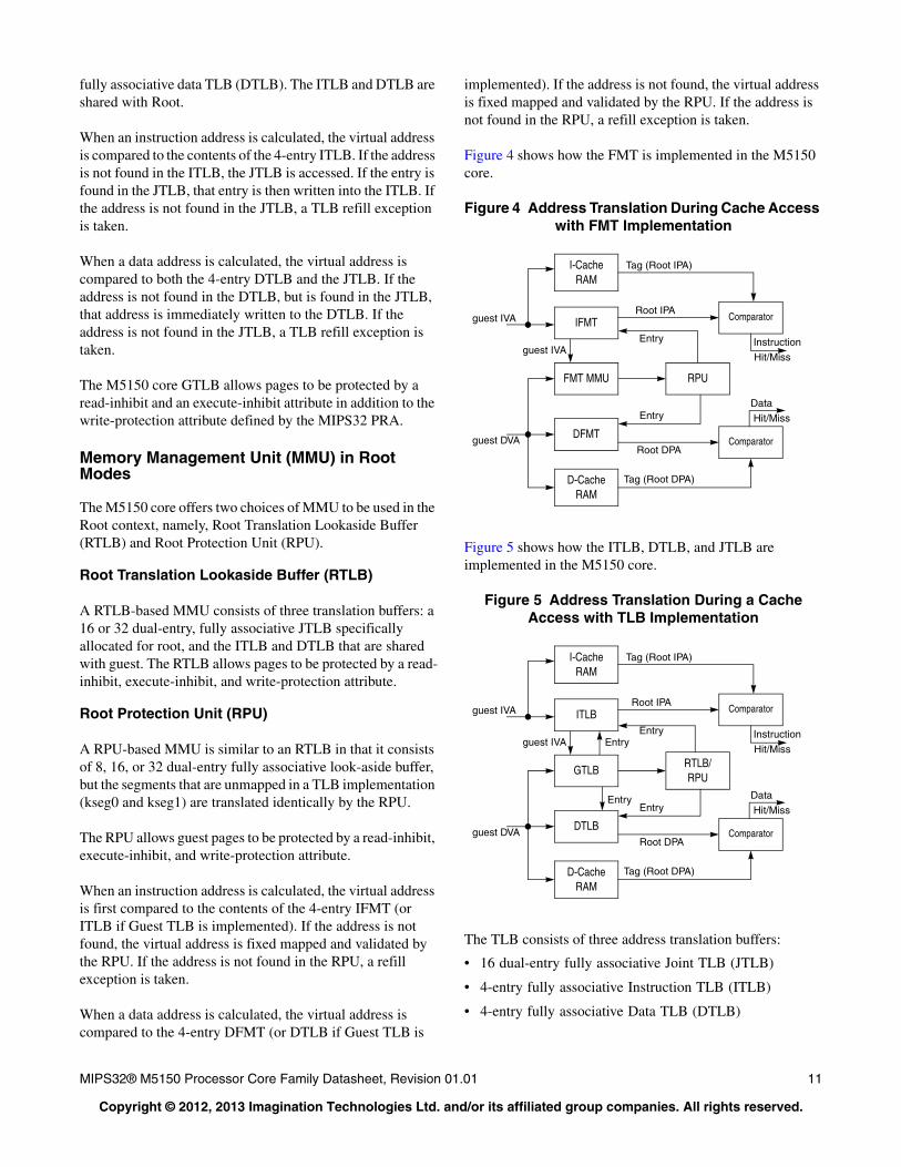
Fixed Mapping Translation (FMT)
A FMT is smaller and simpler than a TLB. Like a TLB, the FMT performs virtual-to-physical address translation and provides attributes for the different segments. Those segments that are unmapped in a TLB implementation (kseg0 and kseg1) are translated identically by the FMT.
Guest Translation Lookaside Buffer (GTLB)
A GTLB-based MMU consists of three translation buffers: a 16 or 32 dual-entry fully associative Joint TLB (JTLB), a 4-entry fully associative Instruction TLB (ITLB), and a 4-entry
kuseg
kseg0
kseg1
kseg2
kseg3
0x00000000
0x7FFFFFFF0x80000000
0x9FFFFFFF
0xA0000000
0xBFFFFFFF0xC0000000
0xDFFFFFFF
0xE0000000
0xF1FFFFFF
Kernel Virtual Address Space
Unmapped, 512 MBKernel Virtual Address Space
Uncached
Unmapped, 512 MBKernel Virtual Address Space
User Virtual Address Space
1. This space is mapped to memory in user or kernel mode, and by the EJTAG module in debug mode.
0xFF2000000xFF3FFFFF0xFF400000
0xFFFFFFFF
Memory/EJTAG1
Mapped, 2048 MB
Mapped, 512 MB
Memory Mapped
Memory Mapped
MIPS32® M5150 Processor Core Family Datasheet, Revision 01.01 11
Copyright © 2012, 2013 Imagination Technologies Ltd. and/or its affiliated group companies. All rights reserved.
fully associative data TLB (DTLB). The ITLB and DTLB are shared with Root.
When an instruction address is calculated, the virtual address is compared to the contents of the 4-entry ITLB. If the address is not found in the ITLB, the JTLB is accessed. If the entry is found in the JTLB, that entry is then written into the ITLB. If the address is not found in the JTLB, a TLB refill exception is taken.
When a data address is calculated, the virtual address is compared to both the 4-entry DTLB and the JTLB. If the address is not found in the DTLB, but is found in the JTLB, that address is immediately written to the DTLB. If the address is not found in the JTLB, a TLB refill exception is taken.
The M5150 core GTLB allows pages to be protected by a read-inhibit and an execute-inhibit attribute in addition to the write-protection attribute defined by the MIPS32 PRA.
Memory Management Unit (MMU) in Root Modes
The M5150 core offers two choices of MMU to be used in the Root context, namely, Root Translation Lookaside Buffer (RTLB) and Root Protection Unit (RPU).
Root Translation Lookaside Buffer (RTLB)
A RTLB-based MMU consists of three translation buffers: a 16 or 32 dual-entry, fully associative JTLB specifically allocated for root, and the ITLB and DTLB that are shared with guest. The RTLB allows pages to be protected by a read-inhibit, execute-inhibit, and write-protection attribute.
Root Protection Unit (RPU)
A RPU-based MMU is similar to an RTLB in that it consists of 8, 16, or 32 dual-entry fully associative look-aside buffer, but the segments that are unmapped in a TLB implementation (kseg0 and kseg1) are translated identically by the RPU.
The RPU allows guest pages to be protected by a read-inhibit, execute-inhibit, and write-protection attribute.
When an instruction address is calculated, the virtual address is first compared to the contents of the 4-entry IFMT (or ITLB if Guest TLB is implemented). If the address is not found, the virtual address is fixed mapped and validated by the RPU. If the address is not found in the RPU, a refill exception is taken.
When a data address is calculated, the virtual address is compared to the 4-entry DFMT (or DTLB if Guest TLB is
implemented). If the address is not found, the virtual address is fixed mapped and validated by the RPU. If the address is not found in the RPU, a refill exception is taken.
Figure 4 shows how the FMT is implemented in the M5150 core.
Figure 4 Address Translation During Cache Access with FMT Implementation
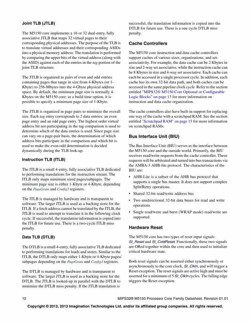
Figure 5 shows how the ITLB, DTLB, and JTLB are implemented in the M5150 core.
Figure 5 Address Translation During a Cache Access with TLB Implementation
The TLB consists of three address translation buffers:
• 16 dual-entry fully associative Joint TLB (JTLB)
• 4-entry fully associative Instruction TLB (ITLB)
• 4-entry fully associative Data TLB (DTLB)
guest IVAEntry
I-CacheRAM
D-CacheRAM
IFMT
DFMT
Entry
guest DVA Comparator
guest IVA Comparator
Tag (Root IPA)
Tag (Root DPA)
Data
Hit/Miss
Hit/Miss
Instruction
Root IPA
Root DPA
FMT MMU RPU
guest IVAEntry
I-CacheRAM
D-CacheRAM
ITLB
GTLB
DTLB
RTLB/RPU
Entry
Entry
Entry
guest DVA Comparator
guest IVA Comparator
Tag (Root IPA)
Tag (Root DPA)
Data
Hit/Miss
Hit/Miss
Instruction
Root DPA
Root IPA
12 MIPS32® M5150 Processor Core Family Datasheet, Revision 01.01
Copyright © 2012, 2013 Imagination Technologies Ltd. and/or its affiliated group companies. All rights reserved.
Joint TLB (JTLB)
The M5150 core implements a 16 or 32 dual-entry, fully associative JTLB that maps 32 virtual pages to their corresponding physical addresses. The purpose of the TLB is to translate virtual addresses and their corresponding ASIDs into a physical memory address. The translation is performed by comparing the upper bits of the virtual address (along with the ASID) against each of the entries in the tag portion of the joint TLB structure.
The JTLB is organized as pairs of even and odd entries containing pages that range in size from 4-Kbytes (or 1-Kbyte) to 256-Mbytes into the 4-Gbyte physical address space. By default, the minimum page size is normally 4-Kbytes on the M5150 core; as a build time option, it is possible to specify a minimum page size of 1-Kbyte.
The JTLB is organized in page pairs to minimize the overall size. Each tag entry corresponds to 2 data entries: an even page entry and an odd page entry. The highest order virtual address bit not participating in the tag comparison is used to determine which of the data entries is used. Since page size can vary on a page-pair basis, the determination of which address bits participate in the comparison and which bit is used to make the even-odd determination is decided dynamically during the TLB look-up.
Instruction TLB (ITLB)
The ITLB is a small 4-entry, fully associative TLB dedicated to performing translations for the instruction stream. The ITLB only maps minimum sized pages/subpages. The minimum page size is either 1-Kbyte or 4-Kbyte, depending on the PageGrain and Config3 registers.
The ITLB is managed by hardware and is transparent to software. The larger JTLB is used as a backing store for the ITLB. If a fetch address cannot be translated by the ITLB, the JTLB is used to attempt to translate it in the following clock cycle. If successful, the translation information is copied into the ITLB for future use. There is a two-cycle ITLB miss penalty.
Data TLB (DTLB)
The DTLB is a small 4-entry, fully associative TLB dedicated to performing translations for loads and stores. Similar to the ITLB, the DTLB only maps either 1-Kbyte or 4-Kbyte pages/subpages depending on the PageGrain and Config3 registers.
The DTLB is managed by hardware and is transparent to software. The larger JTLB is used as a backing store for the DTLB. The JTLB is looked-up in parallel with the DTLB to minimize the DTLB miss penalty. If the JTLB translation is
successful, the translation information is copied into the DTLB for future use. There is a one cycle DTLB miss penalty.
Cache Controllers
The M5150 core instruction and data cache controllers support caches of various sizes, organizations, and set-associativity. For example, the data cache can be 2 Kbytes in size and 2-way set associative, while the instruction cache can be 8 Kbytes in size and 4-way set associative. Each cache can each be accessed in a single processor cycle. In addition, each cache has its own 32-bit data path, and both caches can be accessed in the same pipeline clock cycle. Refer to the section entitled "MIPS32® M5150 Core Optional or Configurable Logic Blocks" on page 13 for more information on instruction and data cache organization.
The cache controllers also have built-in support for replacing one way of the cache with a scratchpad RAM. See the section entitled "Scratchpad RAM" on page 15 for more information on scratchpad RAMs.
Bus Interface Unit (BIU)
The Bus Interface Unit (BIU) serves as the interface between the M5150 core and the outside world. Primarily, the BIU receives read/write requests from the cache controller. These requests will be arbitrated and turned into bus transactions via the AMBA-3 AHB-lite protocol. The characteristics of the BIU are:
• AHB-Lite is a subset of the AHB bus protocol that supports a single bus master. It does not support complex Split/Retry operations.
• Shared 32-bit read/write address bus
• Two unidirectional 32-bit data buses for read and write operations
• Single read/write and burst (WRAP mode) read/write are supported.
Hardware Reset
The M5150 core has two types of reset input signals: SI_Reset and SI_ColdReset. Functionally, these two signals are ORed together within the core and then used to initialize critical hardware state.
Both reset signals can be asserted either synchronously or asynchronously to the core clock, SI_ClkIn, and will trigger a Reset exception. The reset signals are active high and must be asserted for a minimum of 5 SI_ClkIn cycles. The falling edge triggers the Reset exception.
MIPS32® M5150 Processor Core Family Datasheet, Revision 01.01 13
Copyright © 2012, 2013 Imagination Technologies Ltd. and/or its affiliated group companies. All rights reserved.
The primary difference between the two reset signals is that SI_Reset sets a bit in the Status register; this bit could be used by software to distinguish between the two reset signals, if desired. The reset behavior is summarized in Table 5.
One (or both) of the reset signals must be asserted at power-on or whenever hardware initialization of the core is desired. A power-on reset typically occurs when the machine is first turned on. A hard reset usually occurs when the machine is already on and the system is rebooted.
In debug mode, EJTAG can request that a soft reset (via the SI_Reset pin) be masked. It is system-dependent whether this functionality is supported. In normal mode, the SI_Reset pin cannot be masked. The SI_ColdReset pin is never masked.
Power Management
The M5150 core offers a number of power management features, including low-power design, active power management, and power-down modes of operation. The core is a static design that supports slowing or halting the clocks, which reduces system power consumption during idle periods.
The M5150 core provides two mechanisms for system-level low-power support:
• Register-controlled power management
• Instruction-controlled power management
Register-Controlled Power Management
The RP bit in the CP0 Status register provides a software mechanism for placing the system into a low-power state. The state of the RP bit is available externally via the SI_RP signal. The external agent then decides whether to place the device in a low-power mode, such as reducing the system clock frequency.
Three additional bits,StatusEXL, StatusERL, and DebugDM support the power management function by allowing the user
to change the power state if an exception or error occurs while the M5150 core is in a low-power state. Depending on what type of exception is taken, one of these three bits will be asserted and reflected on the SI_EXL, SI_ERL, or EJ_DebugM outputs. The external agent can look at these signals and determine whether to leave the low-power state to service the exception.
The following four power-down signals are part of the system interface and change state as the corresponding bits in the CP0 registers are set or cleared:
• The SI_RP signal represents the state of the RP bit (27) in the CP0 Status register.
• The SI_EXL signal represents the state of the EXL bit (1) in the CP0 Status register.
• The SI_ERL signal represents the state of the ERL bit (2) in the CP0 Status register.
• The EJ_DebugM signal represents the state of the DM bit (30) in the CP0 Debug register.
Instruction-Controlled Power Management
The second mechanism for invoking power-down mode is by executing the WAIT instruction. When the WAIT instruction is executed, the internal clock is suspended; however, the internal timer and some of the input pins (SI_Int[5:0], SI_NMI, SI_Reset, and SI_ColdReset) continue to run. Once the CPU is in instruction-controlled power management mode, any interrupt, NMI, or reset condition causes the CPU to exit this mode and resume normal operation.
The M5150 core asserts the SI_Sleep signal, which is part of the system interface bus, whenever the WAIT instruction is executed. The assertion of SI_Sleep indicates that the clock has stopped and the M5150 core is waiting for an interrupt.
Local clock gating
The majority of the power consumed by the M5150 core is in the clock tree and clocking registers. The core has support for extensive use of local gated-clocks. Power-conscious implementors can use these gated clocks to significantly reduce power consumption within the core.
MIPS32® M5150 Core Optional or Configurable Logic Blocks
The M5150 core contains several optional or configurable logic blocks, shown as shaded in the block diagram in Figure 1.
Table 5 Reset Types
SI_Reset SI_ColdReset Action
0 0 Normal operation, no reset.
1 0 Reset exception; sets StatusSR bit.
X 1 Reset exception.
14 MIPS32® M5150 Processor Core Family Datasheet, Revision 01.01
Copyright © 2012, 2013 Imagination Technologies Ltd. and/or its affiliated group companies. All rights reserved.
Instruction Cache
The instruction cache is an optional on-chip memory block of up to 64 Kbytes. Because the instruction cache is virtually indexed, the virtual-to-physical address translation occurs in parallel with the cache access rather than having to wait for the physical address translation. The tag holds 22 bits of physical address, a valid bit, and a lock bit. The LRU replacement bits (0-6b per set depending on associativity) are stored in a separate array.
The instruction cache block also contains and manages the instruction line fill buffer. Besides accumulating data to be written to the cache, instruction fetches that reference data in the line fill buffer are serviced either by a bypass of that data, or data coming from the external interface. The instruction cache control logic controls the bypass function.
The M5150 core supports instruction-cache locking. Cache locking allows critical code or data segments to be locked into the cache on a “per-line” basis, enabling the system programmer to maximize the efficiency of the system cache.
The cache-locking function is always available on all instruction-cache entries. Entries can then be marked as locked or unlocked on a per entry basis using the CACHE instruction.
Data Cache
The data cache is an optional on-chip memory block of up to 64 Kbytes. This virtually indexed, physically tagged cache is protected. Because the data cache is virtually indexed, the virtual-to-physical address translation occurs in parallel with the cache access. The tag holds 22 bits of physical address, a valid bit, and a lock bit. There is an additional array holding dirty bits and LRU replacement algorithm bits (0-6b depending on associativity) for each set of the cache.
In addition to instruction-cache locking, the M5150 core also supports a data-cache locking mechanism identical to the instruction cache. Critical data segments are locked into the cache on a “per-line” basis. The locked contents can be updated on a store hit, but cannot be selected for replacement on a cache miss.
The cache-locking function is always available on all data cache entries. Entries can then be marked as locked or unlocked on a per-entry basis using the CACHE instruction.
Cache Memory Configuration
The M5150 core incorporates on-chip instruction and data caches that can each be accessed in a single processor cycle.
Each cache has its own 32-bit data path and can be accessed in the same pipeline clock cycle. Table 6 lists the M5150 core instruction and data cache attributes.
Cache Protocols
The M5150 core supports the following cache protocols:
• Uncached: Addresses in a memory area indicated as uncached are not read from the cache. Stores to such addresses are written directly to main memory, without changing cache contents.
• Write-through, no write allocate: Loads and instruction fetches first search the cache, reading main memory only if the desired data does not reside in the cache. On data store operations, the cache is first searched to see if the target address is cache resident. If it is resident, the cache contents are updated, and main memory is also written. If the cache look-up misses, only main memory is written.
• Write-through, write allocate: Similar to above, but stores missing in the cache will cause a cache refill. The store data is then written to both the cache and main memory.
• Write-back, write allocate: Stores that miss in the cache will cause a cache refill. Store data, however, is only written to the cache. Caches lines that are written by stores will be marked as dirty. If a dirty line is selected for replacement, the cache line will be written back to main memory.
Table 6 Instruction and Data Cache Attributes
Parameter Instruction Data
Size 0 - 64 Kbytes 0 - 64 Kbytes
Organization 1 - 4 way set asso-ciative
1 - 4 way set asso-ciative
Line Size 16 bytes 16 bytes
Read Unit 32 bits 32 bits
Write Policies NA write-through with write allocate,write-through without write allo-cate,write-back with write allocate
Miss restart after transfer of
miss word miss word
Cache Locking per line per line
MIPS32® M5150 Processor Core Family Datasheet, Revision 01.01 15
Copyright © 2012, 2013 Imagination Technologies Ltd. and/or its affiliated group companies. All rights reserved.
Scratchpad RAM
The M5150 core also supports replacing up to one way of each cache with a scratchpad RAM. Scratchpad RAM is accessed via independent external pin interfaces for instruction and data scratchpads. The external block which connects to a scratchpad interface is user-defined and can consist of a variety of devices. The main requirement is that it must be accessible with timing similar to an internal cache RAM. Normally, this means that an index will be driven one cycle, a tag will be driven the following clock, and the scratchpad must return a hit signal and the data in the second clock. The scratchpad can easily contain a large RAM/ROM or memory-mapped registers. Unlike the fixed single-cycle cache timing, however, the scratchpad interface can also accommodate back-stalling the core pipeline if data is not available in a single clock. This back-stalling capability can be useful for operations which require multi-cycle latency. It can also be used to enable arbitration of external accesses to a shared scratchpad memory.
The core’s functional interface to a scratchpad RAM is slightly different from the interface to a regular cache RAM. Additional index bits allow access to a larger array, with 1MB of scratchpad RAM versus 4KB for a cache way. These bits come from the virtual address, so on a M5150 core care must be taken to avoid virtual aliasing. The core does not automatically refill the scratchpad way and will not select it for replacement on cache misses.
microMIPS™ ISA
The M5150 core supports the microMIPS ISA, which contains all MIPS32 ISA instructions (except for branch- likely instructions) in a new 32-bit encoding scheme, with some of the commonly used instructions also available in 16-bit encoded format. This ISA improves code density through the additional 16-bit instructions while maintaining a performance similar to MIPS32 mode. In microMIPS mode, 16-bit or 32-bit instructions will be fetched and recoded to legacy MIPS32 instruction opcodes in the pipeline’s I stage, so that the M5150 core can have the same microAptiv™ UP microarchitecture. Because the microMIPS instruction stream can be intermixed with 16-bit halfword or 32-bit word size instructions on halfword or word boundaries, additional logic is in place to address the word misalignment issues, thus minimizing performance loss.
Depending on the optimization preference when both MIPS32 and microMIPS ISAs are configured, the microMIPS can be configured in performance mode, with multiple recoding blocks being executed in parallel with Tag compare for each Way Associativity, or with a single recoding block after the Tag compare logic to improve area usage.
DSP Module
The M5150 core implements an optional DSP Module to benefit a wide range of DSP, Media, and DSP-like algorithms. The DSP module is highly integrated with the Execution Unit and the MDU in order to share common logic and to include support for operations on fractional data types, saturating arithmetic, and register SIMD operations. Fractional data types Q15 and Q31 are supported. Register SIMD operations can perform up to four simultaneous add, subtract, or shift operations and two simultaneous multiply operations.
In addition, the DSP Module includes some key features that efficiently address specific problems often encountered in DSP applications. These include, for example, support for complex multiply, variable-bit insert and extract, and implementation and use of virtual circular buffers. The extension also makes available three additional sets of HI-LO accumulators to better facilitate common accumulate functions such as filter operation and convolutions.
Floating Point Unit (FPU)
The M5150 core Floating Point Unit (FPU) implements the MIPS Instruction Set Architecture for floating-point computation. The implementation supports the ANSI/IEEE Standard 754 (IEEE Standard for Binary Floating-Point Arithmetic) for single and double precision data formats. The FPU can be programmed to have thirty-two 32-bit or 64-bit floating-point registers used for floating point operations.
The performance is optimized for single precision formats. Most instructions have one FPU cycle throughput and four FPU cycle latency. The FPU implements the multiply-add (MADD) and multiply-sub (MSUB) instructions with intermediate rounding after the multiply function. The result is guaranteed to be the same as executing a MUL and an ADD instruction separately, but the instruction latency, instruction fetch, dispatch bandwidth, and the total number of register accesses are improved.
IEEE denormalized input operands and results are supported by hardware for some instructions. IEEE denormalized results are not supported by hardware in general, but a fast flush-to-zero mode is provided to optimize performance. The fast flush-to-zero mode is enabled through the FCCR register, and use of this mode is recommended for best performance when denormalized results are generated.
The FPU has a separate pipeline for floating point instruction execution. This pipeline operates in parallel with the integer core pipeline and does not stall when the integer pipeline stalls. This allows long-running FPU operations, such as divide or square root, to be partially masked by system stalls and/or other integer unit instructions. Arithmetic instructions
16 MIPS32® M5150 Processor Core Family Datasheet, Revision 01.01
Copyright © 2012, 2013 Imagination Technologies Ltd. and/or its affiliated group companies. All rights reserved.
are always dispatched and completed in order, but loads and stores can complete out of order. The exception model is ‘precise’ at all times.
FPU Pipeline
The FPU implements a high-performance 7-stage pipeline:
• Decode, register read and unpack (FR stage)
• Multiply tree - double pumped for double (M1 stage)
• Multiply complete (M2 stage)
• Addition first step (A1 stage)
• Addition second and final step (A2 stage)
• Packing to IEEE format (FP stage)
• Register writeback (FW stage)
The FPU implements a bypass mechanism that allows the result of an operation to be forwarded directly to the instruction that needs it without having to write the result to the FPU register and then read it back.
Figure 6 shows the FPU pipeline.
Figure 6 FPU Pipeline.
FPU Instruction Latencies and Repeat Rates
Table 7 contains the floating point instruction latencies and repeat rates for the M5150 core. In this table, ‘Latency’ refers to the number of FPU cycles necessary for the first instruction to produce the result needed by the second instruction. The ‘Repeat Rate’ refers to the maximum rate at which an instruction can be executed per FPU cycle.
Coprocessor 2 Interface
The M5150 core can be configured to have an interface for an on-chip coprocessor. This coprocessor can be tightly coupled to the processor core, allowing high-performance solutions integrating a graphics accelerator or DSP, for example.
The coprocessor interface is extensible and standardized on MIPS cores, allowing for design reuse. The M5150 core supports a subset of the full coprocessor interface standard:
Table 7 M5150 Core FPU Latency and Repeat Rate
Opcode*
Latency (FPU cycles)
Repeat Rate (FPU cycles)
ABS.[S,D], NEG.[S,D], ADD.[S,D], SUB.[S,D], C.cond.[S,D], MUL.S
4 1
* Format: S = Single, D = Double, W = Word, L = Long-word
FR M1 M2 A1 A2 FP FWFPU Pipeline
Bypass
Bypass
Bypass
FPU Clock
MADD.S, MSUB.S, NMADD.S, NMSUB.S, CABS.cond.[S,D]
4 1
CVT.D.S, CVT.PS.PW, CVT.[S,D].[W,L]
4 1
CVT.S.D, CVT.[W,L].[S,D], CEIL.[W,L].[S,D], FLOOR.[W,L].[S,D], ROUND.[W,L].[S,D], TRUNC.[W,L].[S,D]
4 1
MOV.[S,D], MOVF.[S,D], MOVN.[S,D], MOVT.[S,D], MOVZ.[S,D]
4 1
MUL.D 5 2
MADD.D, MSUB.D, NMADD.D, NMSUB.D
5 2
RECIP.S 13 10
RECIP.D 26 21
RSQRT.S 17 14
RSQRT.D 36 31
DIV.S, SQRT.S 17 14
DIV.D, SQRT.D 32 29
MTC1, DMTC1, LWC1, LDC1, LDXC1, LUXC1, LWXC1
4 1
MFC1, DMFC1, SWC1, SDC1, SDXC1, SUXC1, SWXC1
1 1
Table 7 M5150 Core FPU Latency and Repeat Rate (Continued)
Opcode*
Latency (FPU cycles)
Repeat Rate (FPU cycles)
* Format: S = Single, D = Double, W = Word, L = Long-word
MIPS32® M5150 Processor Core Family Datasheet, Revision 01.01 17
Copyright © 2012, 2013 Imagination Technologies Ltd. and/or its affiliated group companies. All rights reserved.
32b data transfer, no Coprocessor 1 support, single issue in-order data transfer to coprocessor, one out-of-order data transfer from coprocessor.
The coprocessor interface is designed to ease integration with customer IP. The interface allows high-performance communication between the core and coprocessor. There are no late or critical signals on the interface.
CorExtend® User-defined InstructionExtensions
An optional CorExtend User-defined Instruction (UDI) block enables the implementation of a small number of application-specific instructions that are tightly coupled to the core’s execution unit. The interface to the UDI block is external to the M5150 core.
Such instructions may operate on a general-purpose register, immediate data specified by the instruction word, or local state stored within the UDI block. The destination may be a general-purpose register or local UDI state. The operation may complete in one cycle or multiple cycles, if desired.
Anti-Tamper Security Features
The core provides security features that counter side-channel attacks attempting to reveal the code or data running on the processor.
Random slips can be generated in order to disguise the timing and power profile of an algorithm executing on the processor. This reduces the core’s vulnerability to side channel attacks. Power management techniques are used to ensure that the power profile of a random slip is indistinguishable from the power profile of the executing instructions.
The core contains two pseudo random number generators. One is a general- purpose generator for use by software. The other is used by the random slip and random cache-line refill order logic. The generators may optionally be designed by the implementor of the core, thus allowing the quality of the pseudo random number sequences to be suited for any needs.
The optional scrambling module allows scrambling of the data in SPRAM modules and in all RAM arrays associated with the cache. Scrambling can be done on both the data and address bus on the RAM arrays. For the cache module, WS and Tag RAM arrays as well as the data RAM array can be scrambled. The scrambling module has a configuration interface that allows the scrambling engine to be configured from software. The implementation of the scrambling module is defined by the implementor of the core. This assures the widest possible flexibility in the choice of scrambling
schemes and allows the implementor to decide on the trade-off between area and speed versus security.
EJTAG Debug Support
The M5150 core provides for an Enhanced JTAG (EJTAG) interface for use in the software debug of application and kernel code. In addition to standard user mode and kernel modes of operation, the M5150 core provides a Debug mode that is entered after a debug exception (derived from a hardware breakpoint, single-step exception, etc.) is taken and continues until a debug exception return (DERET) instruction is executed. During this time, the processor executes the debug exception handler routine.
The EJTAG interface operates through the Test Access Port (TAP), a serial communication port used for transferring test data in and out of the M5150 core. In addition to the standard JTAG instructions, special instructions defined in the EJTAG specification specify which registers are selected and how they are used.
Debug Registers
Four debug registers (DEBUG, DEBUG2, DEPC, and DESAVE) have been added to the MIPS Coprocessor 0 (CP0) register set. The DEBUG and DEBUG2 registers show the cause of the debug exception and are used for setting up single-step operations. The DEPC (Debug Exception Program Counter) register holds the address on which the debug exception was taken, which is used to resume program execution after the debug operation finishes. Finally, the DESAVE (Debug Exception Save) register enables the saving of general-purpose registers used during execution of the debug exception handler.
To exit debug mode, a Debug Exception Return (DERET) instruction is executed. When this instruction is executed, the system exits debug mode, allowing normal execution of application and system code to resume.
EJTAG Hardware Breakpoints
There are several types of simple hardware breakpoints defined in the EJTAG specification. These stop the normal operation of the CPU and force the system into debug mode. There are two types of simple hardware breakpoints implemented in the M5150 core: Instruction breakpoints and Data breakpoints. Additionally, complex hardware breakpoints can be included, which allow detection of more intricate sequences of events.
The M5150 core can be configured with the following breakpoint options:
18 MIPS32® M5150 Processor Core Family Datasheet, Revision 01.01
Copyright © 2012, 2013 Imagination Technologies Ltd. and/or its affiliated group companies. All rights reserved.
• No data or instruction, or complex breakpoints
• One data and two instruction breakpoints, without complex breakpoints
• Two data and four instruction breakpoints, without complex breakpoints
• Two data and six instruction breakpoints, with or without complex breakpoints
• Four data and eight instruction breakpoints, with or without complex breakpoints
Instruction breakpoints occur on instruction execution operations, and the breakpoint is set on the virtual address.Instruction breakpoints can also be made on the ASID value used by the MMU. A mask can be applied to the virtual address to set breakpoints on a binary range of instructions.
Data breakpoints occur on load/store transactions, and the breakpoint is set on a set of virtual address and ASID values, with the same single address or binary address range as the Instruction breakpoint. Data breakpoints can be set on a load, a store, or both. Data breakpoints can also be set to match on the operand value of the load/store operation, with byte-granularity masking. Finally, masks can be applied to both the virtual address and the load/store value.
In addition, the M5150 core has a configurable feature to support data and instruction address-range triggered breakpoints, where a breakpoint can occur when a virtual address is either within or outside a pair of 32-bit addresses. Unlike the traditional address-mask control, address-range triggering is not restricted to a power-of-two binary boundary.
Complex breakpoints utilize the simple instruction and data breakpoints and break when combinations of events are seen. Complex break features include:
• Pass Counters - Each time a matching condition is seen, a counter is decremented. The break or trigger will only be enabled when the counter has counted down to 0.
• Tuples - A tuple is the pairing of an instruction and a data breakpoint. The tuple will match if both the virtual address of the load or store instruction matches the instruction breakpoint, and the data breakpoint of the resulting load or store address and optional data value matches.
• Priming - This allows a breakpoint to be enabled only after other break conditions have been met. Also called sequential or armed triggering.
• Qualified - This feature uses a data breakpoint to qualify when an instruction breakpoint can be taken. Once a load matches the data address and the data value, the
instruction break will be enabled. If a load matches the address, but has mis-matching data, the instruction break will be disabled.
Performance Counters
Performance counters are used to accumulate occurrences of internal predefined events/cycles/conditions for program analysis, debug, or profiling. A few examples of event types are clock cycles, instructions executed, specific instruction types executed, loads, stores, exceptions, and cycles while the CPU is stalled. There are two, 32-bit counters. Each can count one of the 64 internal predefined events selected by a corresponding control register. A counter overflow can be programmed to generate an interrupt, where the interrupt handler software can maintain larger total counts.
PC/Address Sampling
This sampling function is used for program profiling and hot-spots analysis. Instruction PC and/or Load/Store addresses can be sampled periodically. The result is scanned out through the EJTAG port. The Debug Control Register (DCR) is used to specify the sample period and the sample trigger.
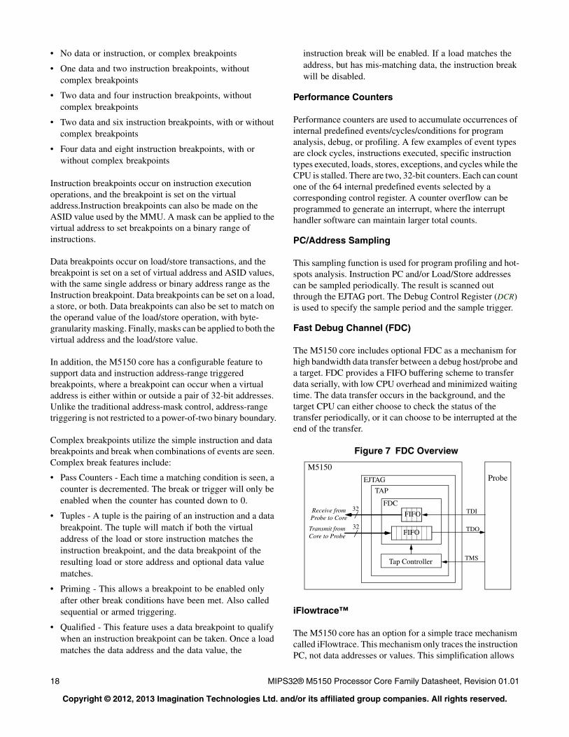
Fast Debug Channel (FDC)
The M5150 core includes optional FDC as a mechanism for high bandwidth data transfer between a debug host/probe and a target. FDC provides a FIFO buffering scheme to transfer data serially, with low CPU overhead and minimized waiting time. The data transfer occurs in the background, and the target CPU can either choose to check the status of the transfer periodically, or it can choose to be interrupted at the end of the transfer.
Figure 7 FDC Overview
iFlowtrace™
The M5150 core has an option for a simple trace mechanism called iFlowtrace. This mechanism only traces the instruction PC, not data addresses or values. This simplification allows
M5150ProbeEJTAG
TAP
FDC
Tap Controller
TDI
TDO
TMS
FIFOReceive from Probe to Core
Transmit from Core to Probe FIFO
32
32
MIPS32® M5150 Processor Core Family Datasheet, Revision 01.01 19
Copyright © 2012, 2013 Imagination Technologies Ltd. and/or its affiliated group companies. All rights reserved.
the trace block to be smaller and the trace compression to be more efficient. iFlowtrace memory can be configured as off-chip, on-chip, or both.
iFlowtrace also offers special-event trace modes when normal tracing is disabled, namely:
• Function Call/Return and Exception Tracing mode to trace the PC value of function calls and returns and/or exceptions and returns.
• Breakpoint Match mode traces the breakpoint ID of a matching breakpoint and, for data breakpoints, the PC value of the instruction that caused it.
• Filtered Data Tracing mode traces the ID of a matching data breakpoint, the load or store data value, access type and memory access size, and the low-order address bits of the memory access, which is useful when the data breakpoint is set up to match a binary range of addresses.
• User Trace Messages. The user can instrument their code to add their own 32-bit value messages into the trace by writing to the Cop0 UTM register.
• Delta Cycle mode works in combination with the above trace modes to provide a timestamp between stored events. It reports the number of cycles that have elapsed since the last message was generated and put into the trace.
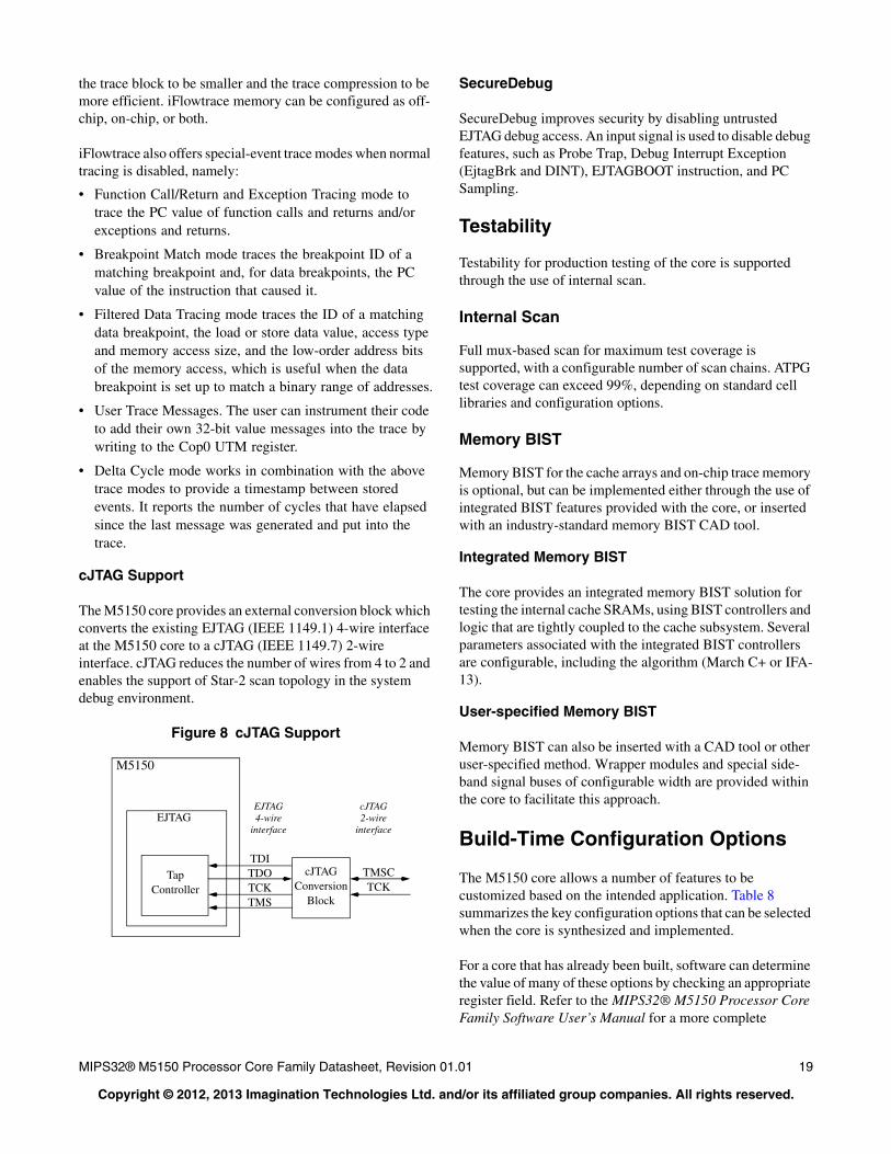
cJTAG Support
The M5150 core provides an external conversion block which converts the existing EJTAG (IEEE 1149.1) 4-wire interface at the M5150 core to a cJTAG (IEEE 1149.7) 2-wire interface. cJTAG reduces the number of wires from 4 to 2 and enables the support of Star-2 scan topology in the system debug environment.
Figure 8 cJTAG Support
SecureDebug
SecureDebug improves security by disabling untrusted EJTAG debug access. An input signal is used to disable debug features, such as Probe Trap, Debug Interrupt Exception (EjtagBrk and DINT), EJTAGBOOT instruction, and PC Sampling.
Testability
Testability for production testing of the core is supported through the use of internal scan.
Internal Scan
Full mux-based scan for maximum test coverage is supported, with a configurable number of scan chains. ATPG test coverage can exceed 99%, depending on standard cell libraries and configuration options.
Memory BIST
Memory BIST for the cache arrays and on-chip trace memory is optional, but can be implemented either through the use of integrated BIST features provided with the core, or inserted with an industry-standard memory BIST CAD tool.
Integrated Memory BIST
The core provides an integrated memory BIST solution for testing the internal cache SRAMs, using BIST controllers and logic that are tightly coupled to the cache subsystem. Several parameters associated with the integrated BIST controllers are configurable, including the algorithm (March C+ or IFA-13).
User-specified Memory BIST
Memory BIST can also be inserted with a CAD tool or other user-specified method. Wrapper modules and special side-band signal buses of configurable width are provided within the core to facilitate this approach.
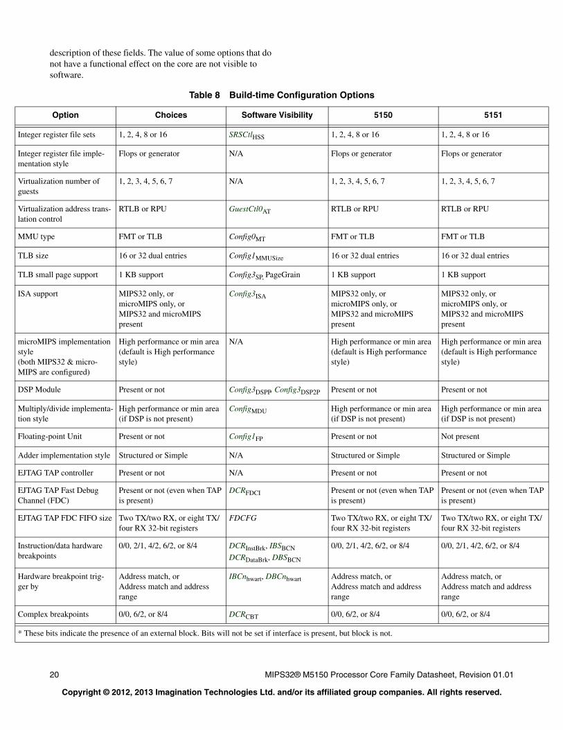
Build-Time Configuration Options
The M5150 core allows a number of features to be customized based on the intended application. Table 8 summarizes the key configuration options that can be selected when the core is synthesized and implemented.
For a core that has already been built, software can determine the value of many of these options by checking an appropriate register field. Refer to the MIPS32® M5150 Processor Core Family Software User’s Manual for a more complete
Tap Controller
M5150
EJTAGEJTAG 4-wire
interface
TDI TDO TCK TMS
TMSC TCK
cJTAG Conversion
Block
cJTAG 2-wire
interface
20 MIPS32® M5150 Processor Core Family Datasheet, Revision 01.01
Copyright © 2012, 2013 Imagination Technologies Ltd. and/or its affiliated group companies. All rights reserved.
description of these fields. The value of some options that do not have a functional effect on the core are not visible to software.
Table 8 Build-time Configuration Options
Option Choices Software Visibility 5150 5151
Integer register file sets 1, 2, 4, 8 or 16 SRSCtlHSS 1, 2, 4, 8 or 16 1, 2, 4, 8 or 16
Integer register file imple-mentation style
Flops or generator N/A Flops or generator Flops or generator
Virtualization number of guests
1, 2, 3, 4, 5, 6, 7 N/A 1, 2, 3, 4, 5, 6, 7 1, 2, 3, 4, 5, 6, 7
Virtualization address trans-lation control
RTLB or RPU GuestCtl0AT RTLB or RPU RTLB or RPU
MMU type FMT or TLB Config0MT FMT or TLB FMT or TLB
TLB size 16 or 32 dual entries Config1MMUSize 16 or 32 dual entries 16 or 32 dual entries
TLB small page support 1 KB support Config3SP, PageGrain 1 KB support 1 KB support
ISA support MIPS32 only, ormicroMIPS only, orMIPS32 and microMIPS present
Config3ISA MIPS32 only, ormicroMIPS only, orMIPS32 and microMIPS present
MIPS32 only, ormicroMIPS only, orMIPS32 and microMIPS present
microMIPS implementation style(both MIPS32 & micro-MIPS are configured)
High performance or min area(default is High performance style)
N/A High performance or min area(default is High performance style)
High performance or min area(default is High performance style)
DSP Module Present or not Config3DSPP, Config3DSP2P Present or not Present or not
Multiply/divide implementa-tion style
High performance or min area (if DSP is not present)
ConfigMDU High performance or min area (if DSP is not present)
High performance or min area (if DSP is not present)
Floating-point Unit Present or not Config1FP Present or not Not present
Adder implementation style Structured or Simple N/A Structured or Simple Structured or Simple
EJTAG TAP controller Present or not N/A Present or not Present or not
EJTAG TAP Fast Debug Channel (FDC)
Present or not (even when TAP is present)
DCRFDCI Present or not (even when TAP is present)
Present or not (even when TAP is present)
EJTAG TAP FDC FIFO size Two TX/two RX, or eight TX/four RX 32-bit registers
FDCFG Two TX/two RX, or eight TX/four RX 32-bit registers
Two TX/two RX, or eight TX/four RX 32-bit registers
Instruction/data hardware breakpoints
0/0, 2/1, 4/2, 6/2, or 8/4 DCRInstBrk, IBSBCN
DCRDataBrk, DBSBCN
0/0, 2/1, 4/2, 6/2, or 8/4 0/0, 2/1, 4/2, 6/2, or 8/4
Hardware breakpoint trig-ger by
Address match, orAddress match and address range
IBCnhwart, DBCnhwart Address match, orAddress match and address range
Address match, orAddress match and address range
Complex breakpoints 0/0, 6/2, or 8/4 DCRCBT 0/0, 6/2, or 8/4 0/0, 6/2, or 8/4
* These bits indicate the presence of an external block. Bits will not be set if interface is present, but block is not.
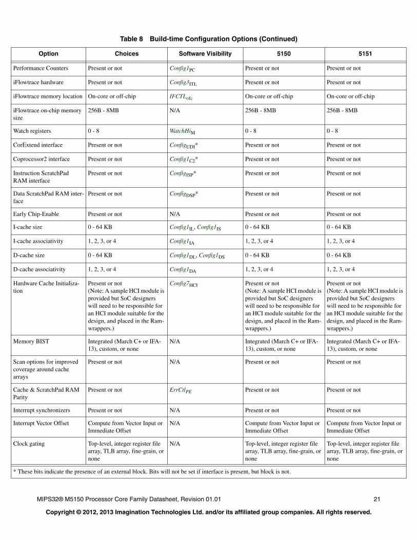
MIPS32® M5150 Processor Core Family Datasheet, Revision 01.01 21
Copyright © 2012, 2013 Imagination Technologies Ltd. and/or its affiliated group companies. All rights reserved.
Performance Counters Present or not Config1PC Present or not Present or not
iFlowtrace hardware Present or not Config3ITL Present or not Present or not
iFlowtrace memory location On-core or off-chip IFCTLofc On-core or off-chip On-core or off-chip
iFlowtrace on-chip memory size
256B - 8MB N/A 256B - 8MB 256B - 8MB
Watch registers 0 - 8 WatchHiM 0 - 8 0 - 8
CorExtend interface Present or not ConfigUDI* Present or not Present or not
Coprocessor2 interface Present or not Config1C2* Present or not Present or not
Instruction ScratchPad RAM interface
Present or not ConfigISP* Present or not Present or not
Data ScratchPad RAM inter-face
Present or not ConfigDSP* Present or not Present or not
Early Chip-Enable Present or not N/A Present or not Present or not
I-cache size 0 - 64 KB Config1IL, Config1IS 0 - 64 KB 0 - 64 KB
I-cache associativity 1, 2, 3, or 4 Config1IA 1, 2, 3, or 4 1, 2, 3, or 4
D-cache size 0 - 64 KB Config1DL, Config1DS 0 - 64 KB 0 - 64 KB
D-cache associativity 1, 2, 3, or 4 Config1DA 1, 2, 3, or 4 1, 2, 3, or 4
Hardware Cache Initializa-tion
Present or not(Note: A sample HCI module is provided but SoC designers will need to be responsible for an HCI module suitable for the design, and placed in the Ram-wrappers.)
Config7HCI Present or not(Note: A sample HCI module is provided but SoC designers will need to be responsible for an HCI module suitable for the design, and placed in the Ram-wrappers.)
Present or not(Note: A sample HCI module is provided but SoC designers will need to be responsible for an HCI module suitable for the design, and placed in the Ram-wrappers.)
Memory BIST Integrated (March C+ or IFA-13), custom, or none
N/A Integrated (March C+ or IFA-13), custom, or none
Integrated (March C+ or IFA-13), custom, or none
Scan options for improved coverage around cache arrays
Present or not N/A Present or not Present or not
Cache & ScratchPad RAM Parity
Present or not ErrCtlPE Present or not Present or not
Interrupt synchronizers Present or not N/A Present or not Present or not
Interrupt Vector Offset Compute from Vector Input or Immediate Offset
N/A Compute from Vector Input or Immediate Offset
Compute from Vector Input or Immediate Offset
Clock gating Top-level, integer register file array, TLB array, fine-grain, or none
N/A Top-level, integer register file array, TLB array, fine-grain, or none
Top-level, integer register file array, TLB array, fine-grain, or none
Table 8 Build-time Configuration Options (Continued)
Option Choices Software Visibility 5150 5151
* These bits indicate the presence of an external block. Bits will not be set if interface is present, but block is not.
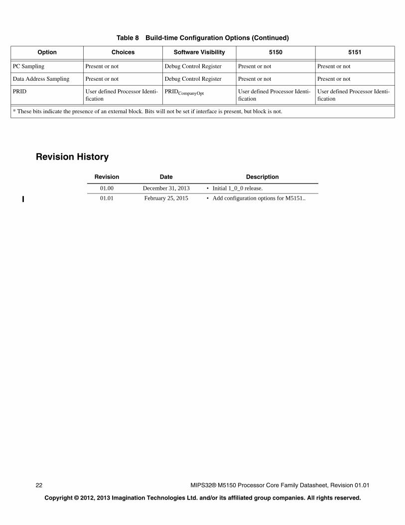
22 MIPS32® M5150 Processor Core Family Datasheet, Revision 01.01
Copyright © 2012, 2013 Imagination Technologies Ltd. and/or its affiliated group companies. All rights reserved.
Revision History
PC Sampling Present or not Debug Control Register Present or not Present or not
Data Address Sampling Present or not Debug Control Register Present or not Present or not
PRID User defined Processor Identi-fication
PRIDCompanyOpt User defined Processor Identi-fication
User defined Processor Identi-fication
Table 8 Build-time Configuration Options (Continued)
Option Choices Software Visibility 5150 5151
* These bits indicate the presence of an external block. Bits will not be set if interface is present, but block is not.
Revision Date Description
01.00 December 31, 2013 • Initial 1_0_0 release.
01.01 February 25, 2015 • Add configuration options for M5151..
MIPS32® M5150 Processor Core Family Datasheet, Revision 01.01 MD00977
Copyright © 2012, 2013 Imagination Technologies Ltd. and/or its affiliated group companies. and/or its affiliated group companies. All rights reserved.
Template: nDb1.03, Built with tags: 2B
Public. This publication contains proprietary information which is subject to change without notice and issupplied ‘as is’, without any warranty of any kind.